US20090140458A1 - Porous template and imprinting stack for nano-imprint lithography - Google Patents
Porous template and imprinting stack for nano-imprint lithographyDownload PDFInfo
- Publication number
- US20090140458A1 US20090140458A1US12/275,998US27599808AUS2009140458A1US 20090140458 A1US20090140458 A1US 20090140458A1US 27599808 AUS27599808 AUS 27599808AUS 2009140458 A1US2009140458 A1US 2009140458A1
- Authority
- US
- United States
- Prior art keywords
- template
- porous
- layer
- porous material
- imprinting stack
- Prior art date
- Legal status (The legal status is an assumption and is not a legal conclusion. Google has not performed a legal analysis and makes no representation as to the accuracy of the status listed.)
- Granted
Links
- 238000001127nanoimprint lithographyMethods0.000titledescription3
- 239000011148porous materialSubstances0.000claimsabstractdescription143
- 239000000463materialSubstances0.000claimsabstractdescription77
- 238000000034methodMethods0.000claimsabstractdescription50
- 238000001459lithographyMethods0.000claimsabstractdescription35
- 239000000758substrateSubstances0.000claimsdescription88
- VYPSYNLAJGMNEJ-UHFFFAOYSA-NSilicium dioxideChemical compoundO=[Si]=OVYPSYNLAJGMNEJ-UHFFFAOYSA-N0.000claimsdescription53
- 239000005350fused silica glassSubstances0.000claimsdescription33
- 238000003892spreadingMethods0.000claimsdescription11
- 230000007480spreadingEffects0.000claimsdescription11
- 229910052814silicon oxideInorganic materials0.000claimsdescription9
- 238000009826distributionMethods0.000claimsdescription7
- 238000000151depositionMethods0.000claimsdescription4
- 230000008569processEffects0.000abstractdescription30
- 238000009792diffusion processMethods0.000abstractdescription9
- 239000010410layerSubstances0.000description172
- 239000007789gasSubstances0.000description58
- 230000035699permeabilityEffects0.000description28
- XKRFYHLGVUSROY-UHFFFAOYSA-NArgonChemical compound[Ar]XKRFYHLGVUSROY-UHFFFAOYSA-N0.000description26
- 229910052734heliumInorganic materials0.000description25
- SWQJXJOGLNCZEY-UHFFFAOYSA-Nhelium atomChemical compound[He]SWQJXJOGLNCZEY-UHFFFAOYSA-N0.000description25
- 239000001307heliumSubstances0.000description24
- 229910052786argonInorganic materials0.000description13
- IJGRMHOSHXDMSA-UHFFFAOYSA-NAtomic nitrogenChemical compoundN#NIJGRMHOSHXDMSA-UHFFFAOYSA-N0.000description10
- 239000010408filmSubstances0.000description8
- 238000004519manufacturing processMethods0.000description8
- QVGXLLKOCUKJST-UHFFFAOYSA-Natomic oxygenChemical compound[O]QVGXLLKOCUKJST-UHFFFAOYSA-N0.000description7
- 239000001301oxygenSubstances0.000description7
- 229910052760oxygenInorganic materials0.000description7
- XUIMIQQOPSSXEZ-UHFFFAOYSA-NSiliconChemical compound[Si]XUIMIQQOPSSXEZ-UHFFFAOYSA-N0.000description6
- 239000003570airSubstances0.000description6
- 238000000059patterningMethods0.000description6
- 229910052710siliconInorganic materials0.000description6
- 239000010703siliconSubstances0.000description6
- 238000005229chemical vapour depositionMethods0.000description5
- 229910052757nitrogenInorganic materials0.000description5
- 239000012466permeateSubstances0.000description5
- 229920000642polymerPolymers0.000description5
- 239000003361porogenSubstances0.000description5
- 239000002131composite materialSubstances0.000description4
- 239000011521glassSubstances0.000description4
- 230000009467reductionEffects0.000description4
- 239000000377silicon dioxideSubstances0.000description4
- 239000012530fluidSubstances0.000description3
- 239000007788liquidSubstances0.000description3
- 230000033001locomotionEffects0.000description3
- 239000000203mixtureSubstances0.000description3
- 229920000620organic polymerPolymers0.000description3
- 238000012856packingMethods0.000description3
- 238000010926purgeMethods0.000description3
- 229920006395saturated elastomerPolymers0.000description3
- 238000004528spin coatingMethods0.000description3
- 238000012546transferMethods0.000description3
- BNCADMBVWNPPIZ-UHFFFAOYSA-N2-n,2-n,4-n,4-n,6-n,6-n-hexakis(methoxymethyl)-1,3,5-triazine-2,4,6-triamineChemical compoundCOCN(COC)C1=NC(N(COC)COC)=NC(N(COC)COC)=N1BNCADMBVWNPPIZ-UHFFFAOYSA-N0.000description2
- 229920003171Poly (ethylene oxide)Polymers0.000description2
- 230000015572biosynthetic processEffects0.000description2
- -1but not limited toSubstances0.000description2
- 230000007547defectEffects0.000description2
- 238000011161developmentMethods0.000description2
- 239000012776electronic materialSubstances0.000description2
- 230000035515penetrationEffects0.000description2
- 238000005240physical vapour depositionMethods0.000description2
- 239000013047polymeric layerSubstances0.000description2
- 238000002360preparation methodMethods0.000description2
- 238000012545processingMethods0.000description2
- 239000010453quartzSubstances0.000description2
- 230000005855radiationEffects0.000description2
- 239000004065semiconductorSubstances0.000description2
- 239000007787solidSubstances0.000description2
- YHQGMYUVUMAZJR-UHFFFAOYSA-Nα-terpineneChemical compoundCC(C)C1=CC=C(C)CC1YHQGMYUVUMAZJR-UHFFFAOYSA-N0.000description2
- ZAXXZBQODQDCOW-UHFFFAOYSA-N1-methoxypropyl acetateChemical compoundCCC(OC)OC(C)=OZAXXZBQODQDCOW-UHFFFAOYSA-N0.000description1
- 241000252506CharaciformesSpecies0.000description1
- 229920003270Cymel®Polymers0.000description1
- WSTYNZDAOAEEKG-UHFFFAOYSA-NMayolNatural productsCC1=C(O)C(=O)C=C2C(CCC3(C4CC(C(CC4(CCC33C)C)=O)C)C)(C)C3=CC=C21WSTYNZDAOAEEKG-UHFFFAOYSA-N0.000description1
- 229910018557Si OInorganic materials0.000description1
- 229910021536ZeoliteInorganic materials0.000description1
- 238000010521absorption reactionMethods0.000description1
- PNEYBMLMFCGWSK-UHFFFAOYSA-Naluminium oxideInorganic materials[O-2].[O-2].[O-2].[Al+3].[Al+3]PNEYBMLMFCGWSK-UHFFFAOYSA-N0.000description1
- 239000012080ambient airSubstances0.000description1
- CFQGDIWRTHFZMQ-UHFFFAOYSA-Nargon heliumChemical compound[He].[Ar]CFQGDIWRTHFZMQ-UHFFFAOYSA-N0.000description1
- 230000008901benefitEffects0.000description1
- 239000005388borosilicate glassSubstances0.000description1
- 239000013590bulk materialSubstances0.000description1
- 239000003054catalystSubstances0.000description1
- 238000012512characterization methodMethods0.000description1
- 238000004140cleaningMethods0.000description1
- 229910052681coesiteInorganic materials0.000description1
- 238000004891communicationMethods0.000description1
- 230000000052comparative effectEffects0.000description1
- 150000001875compoundsChemical class0.000description1
- 229910052906cristobaliteInorganic materials0.000description1
- 239000003431cross linking reagentSubstances0.000description1
- 230000001419dependent effectEffects0.000description1
- 230000008021depositionEffects0.000description1
- 238000013461designMethods0.000description1
- HNPSIPDUKPIQMN-UHFFFAOYSA-Ndioxosilane;oxo(oxoalumanyloxy)alumaneChemical compoundO=[Si]=O.O=[Al]O[Al]=OHNPSIPDUKPIQMN-UHFFFAOYSA-N0.000description1
- 238000003618dip coatingMethods0.000description1
- KPUWHANPEXNPJT-UHFFFAOYSA-NdisiloxaneChemical class[SiH3]O[SiH3]KPUWHANPEXNPJT-UHFFFAOYSA-N0.000description1
- 238000004090dissolutionMethods0.000description1
- 230000000694effectsEffects0.000description1
- 239000011532electronic conductorSubstances0.000description1
- 238000005516engineering processMethods0.000description1
- 229920002313fluoropolymerPolymers0.000description1
- 230000004907fluxEffects0.000description1
- 230000005660hydrophilic surfaceEffects0.000description1
- 230000002209hydrophobic effectEffects0.000description1
- 239000011261inert gasSubstances0.000description1
- 229910010272inorganic materialInorganic materials0.000description1
- 239000011147inorganic materialSubstances0.000description1
- 229920000592inorganic polymerPolymers0.000description1
- 230000003993interactionEffects0.000description1
- 238000010849ion bombardmentMethods0.000description1
- 230000001788irregularEffects0.000description1
- JDSHMPZPIAZGSV-UHFFFAOYSA-NmelamineChemical compoundNC1=NC(N)=NC(N)=N1JDSHMPZPIAZGSV-UHFFFAOYSA-N0.000description1
- 239000012528membraneSubstances0.000description1
- 239000002184metalSubstances0.000description1
- 238000012986modificationMethods0.000description1
- 230000004048modificationEffects0.000description1
- JFNLZVQOOSMTJK-KNVOCYPGSA-NnorborneneChemical compoundC1[C@@H]2CC[C@H]1C=C2JFNLZVQOOSMTJK-KNVOCYPGSA-N0.000description1
- 230000003287optical effectEffects0.000description1
- 150000002894organic compoundsChemical class0.000description1
- 150000001282organosilanesChemical class0.000description1
- 238000000623plasma-assisted chemical vapour depositionMethods0.000description1
- 229920001451polypropylene glycolPolymers0.000description1
- 238000004886process controlMethods0.000description1
- LLHKCFNBLRBOGN-UHFFFAOYSA-Npropylene glycol methyl ether acetateChemical compoundCOCC(C)OC(C)=OLLHKCFNBLRBOGN-UHFFFAOYSA-N0.000description1
- 239000012925reference materialSubstances0.000description1
- 230000001105regulatory effectEffects0.000description1
- 238000011160researchMethods0.000description1
- 230000000717retained effectEffects0.000description1
- 229910052594sapphireInorganic materials0.000description1
- 239000010980sapphireSubstances0.000description1
- HBMJWWWQQXIZIP-UHFFFAOYSA-Nsilicon carbideChemical compound[Si+]#[C-]HBMJWWWQQXIZIP-UHFFFAOYSA-N0.000description1
- 229910010271silicon carbideInorganic materials0.000description1
- LIVNPJMFVYWSIS-UHFFFAOYSA-Nsilicon monoxideInorganic materials[Si-]#[O+]LIVNPJMFVYWSIS-UHFFFAOYSA-N0.000description1
- 238000007711solidificationMethods0.000description1
- 230000008023solidificationEffects0.000description1
- 239000002904solventSubstances0.000description1
- 229910052682stishoviteInorganic materials0.000description1
- 239000000126substanceSubstances0.000description1
- 238000003786synthesis reactionMethods0.000description1
- 238000012360testing methodMethods0.000description1
- 238000000427thin-film depositionMethods0.000description1
- 229910052905tridymiteInorganic materials0.000description1
- 238000007740vapor depositionMethods0.000description1
- 238000009736wettingMethods0.000description1
- 239000010457zeoliteSubstances0.000description1
Images


Classifications
- G—PHYSICS
- G03—PHOTOGRAPHY; CINEMATOGRAPHY; ANALOGOUS TECHNIQUES USING WAVES OTHER THAN OPTICAL WAVES; ELECTROGRAPHY; HOLOGRAPHY
- G03F—PHOTOMECHANICAL PRODUCTION OF TEXTURED OR PATTERNED SURFACES, e.g. FOR PRINTING, FOR PROCESSING OF SEMICONDUCTOR DEVICES; MATERIALS THEREFOR; ORIGINALS THEREFOR; APPARATUS SPECIALLY ADAPTED THEREFOR
- G03F7/00—Photomechanical, e.g. photolithographic, production of textured or patterned surfaces, e.g. printing surfaces; Materials therefor, e.g. comprising photoresists; Apparatus specially adapted therefor
- G03F7/0002—Lithographic processes using patterning methods other than those involving the exposure to radiation, e.g. by stamping
- B—PERFORMING OPERATIONS; TRANSPORTING
- B82—NANOTECHNOLOGY
- B82Y—SPECIFIC USES OR APPLICATIONS OF NANOSTRUCTURES; MEASUREMENT OR ANALYSIS OF NANOSTRUCTURES; MANUFACTURE OR TREATMENT OF NANOSTRUCTURES
- B82Y10/00—Nanotechnology for information processing, storage or transmission, e.g. quantum computing or single electron logic
- B—PERFORMING OPERATIONS; TRANSPORTING
- B82—NANOTECHNOLOGY
- B82Y—SPECIFIC USES OR APPLICATIONS OF NANOSTRUCTURES; MEASUREMENT OR ANALYSIS OF NANOSTRUCTURES; MANUFACTURE OR TREATMENT OF NANOSTRUCTURES
- B82Y40/00—Manufacture or treatment of nanostructures
- Y—GENERAL TAGGING OF NEW TECHNOLOGICAL DEVELOPMENTS; GENERAL TAGGING OF CROSS-SECTIONAL TECHNOLOGIES SPANNING OVER SEVERAL SECTIONS OF THE IPC; TECHNICAL SUBJECTS COVERED BY FORMER USPC CROSS-REFERENCE ART COLLECTIONS [XRACs] AND DIGESTS
- Y10—TECHNICAL SUBJECTS COVERED BY FORMER USPC
- Y10T—TECHNICAL SUBJECTS COVERED BY FORMER US CLASSIFICATION
- Y10T428/00—Stock material or miscellaneous articles
- Y10T428/249921—Web or sheet containing structurally defined element or component
- Y10T428/249953—Composite having voids in a component [e.g., porous, cellular, etc.]
- Y10T428/249978—Voids specified as micro
Definitions
- Nano-fabricationincludes the fabrication of very small structures that have features on the order of 100 nanometers or smaller.
- One application in which nano-fabrication has had a sizeable impactis in the processing of integrated circuits.
- the semiconductor processing industrycontinues to strive for larger production yields while increasing the circuits per unit area formed on a substrate, therefore nano-fabrication becomes increasingly important.
- Nano-fabricationprovides greater process control while allowing continued reduction of the minimum feature dimensions of the structures formed.
- Other areas of development in which nano-fabrication has been employedinclude biotechnology, optical technology, mechanical systems, and the like.
- an imprint lithography template or imprinting stackincludes a porous material defining a multiplicity of pores with an average pore size of at least about 0.4 nm.
- a porosity of the porous materialis at least about 10%.
- the average pore sizeis at least about 0.5 nm or at least about 1.0 nm.
- the porosity of the porous materialmay be at least about 20%.
- the porous materialis an organosilicate low-k material.
- the relative porosity of the porous material with respect to fused silicamay be at least about 20%.
- the porous materialhas a Young's modulus of at least about 2 GPa, at least about 5 GPa, or at least about 10 GPa.
- the porous materialis positioned between a base layer and a cap layer.
- the base layermay include fused silica.
- the base layerincludes recesses, and the porous material is positioned in the recesses.
- the cap layerincludes SiO x , with 1 ⁇ x ⁇ 2.
- a thickness of the cap layermaybe less than about 100 nm, less than about 50 nm, or less than about 20 nm. Protrusions may extend from the cap layer.
- the porous materialis positioned between a substrate and a cap layer.
- the substratemay include silicon.
- forming an imprint lithography templateincludes forming a porous layer on a base layer, and forming a cap layer on the porous layer.
- forming an imprint lithography templateincludes forming a multiplicity of recesses in a base, depositing a porous material in the recesses, and forming a cap layer on the base layer.
- forming an imprint lithography stackincludes forming a porous layer on a substrate, and forming a cap layer on the porous layer. The porous layer defines a multiplicity of pores with an average pore size of at least about 0.4 nm, and the porosity of the porous layer is at least about 10%.
- an imprint lithography methodincludes applying drops of a polymerizable material to an imprinting stack, contacting the polymerizable material with a template, solidifying the polymerizable material, and separating the template from the solidified material.
- the templateincludes a porous material.
- the imprinting stackincludes a porous material.
- the template and the imprinting stackboth include a porous material. The porous material defines a multiplicity of pores with an average pore size of at least about 0.4 nm, and the porosity of the porous material is at least about 10%.
- an imprint lithography methodincludes dispensing drops of a polymerizable material on a surface of an imprinting stack, contacting the polymerizable material with a template, and allowing the polymerizable material to spread to form a substantially continuous layer on the surface of the imprinting stack.
- the template, the imprinting stack, or bothmay include a porous material defining a multiplicity of pores with an average pore size of at least about 0.4 nm, and the porosity of the porous material is at least about 10%.
- Spreading of the polymerizable material to form the substantially continuous layeroccurs in about 80% or less, about 50% or less, or about 20% less of the time required for a similar distribution of a similar polymerizable material to form a substantially continuous layer between a second template and a second imprinting stack, where the second template and the second imprinting stack have an average pore size of less than about 0.4 nm.
- FIG. 1illustrates a simplified side view of a lithographic system.
- FIG. 2illustrates a simplified side view of the substrate shown in FIG. 1 having a patterned layer positioned thereon.
- FIG. 3illustrates porous templates
- FIG. 4illustrates a porous imprinting stack
- FIG. 5illustrates a portion of a layer with porous material in a multiplicity of recesses.
- FIG. 6illustrates an imprint lithography process using a porous template and a porous imprinting stack.
- FIG. 7illustrates an imprint lithography process using a unitary porous template and a porous imprinting stack.
- FIG. 8is a photograph of drops of imprint resist as dispensed on a substrate.
- FIGS. 9A-Dare photographs of drops of imprint resist spreading on an imprinting stack.
- FIGS. 10A-Dare photographs of drops of imprint resist spreading on a porous imprinting stack.
- imprint lithographyAn exemplary nano-fabrication technique in use today is commonly referred to as imprint lithography.
- Exemplary imprint lithography processesare described in detail in numerous publications, such as U.S. Patent Application Publication No. 2004/0065976, U.S. Patent Application Publication No. 2004/0065252, and U.S. Pat. No. 6,936,194, all of which are hereby incorporated by reference herein.
- An imprint lithography technique disclosed in each of the aforementioned U.S. patent application publications and patentincludes formation of a relief pattern in a formable (polymerizable) layer and transferring a pattern corresponding to the relief pattern into an underlying substrate.
- the substratemay be coupled to a motion stage to facilitate positioning for the patterning process.
- the patterning processuses a template spaced apart from the substrate and the formable liquid applied between the template and the substrate.
- the formable liquidis solidified to form a rigid layer that has a pattern conforming to a shape of the surface of the template that contacts the formable liquid.
- the templateis separated from the rigid layer such that the template and the substrate are spaced apart.
- the substrate and the solidified layerare then subjected to additional processes to transfer a relief image into the substrate that corresponds to the pattern in the solidified layer.
- An imprint lithography stackmay include substrate 12 and one or more layers (e.g., an adhesion layer) adhered to the substrate.
- Substrate 12may be coupled to substrate chuck 14 .
- substrate chuck 14is a vacuum chuck.
- Substrate chuck 14may be any chuck including, but not limited to, vacuum, pin-type, groove-type, electromagnetic, and the like, or any combination thereof. Exemplary chucks are described in U.S. Pat. No. 6,873,087, which is hereby incorporated by reference herein.
- Substrate 12 and substrate chuck 14may be further supported by stage 16 .
- Stage 16may provide motion about the x-, y-, and z-axes.
- Stage 16 , substrate 12 , and substrate chuck 14may also be positioned on a base (not shown).
- Template 18Spaced-apart from substrate 12 is a template 18 .
- Template 18may include a mesa 20 extending therefrom towards substrate 12 , mesa 20 having a patterning surface 22 thereon. Further, mesa 20 may be referred to as mold 20 .
- Template 18 and/or mold 20may be formed from such materials including, but not limited to, fused-silica, quartz, silicon, organic polymers, siloxane polymers, borosilicate glass, fluorocarbon polymers, metal, hardened sapphire, and the like, or any combination thereof.
- patterning surface 22comprises features defined by a plurality of spaced-apart recesses 24 and/or protrusions 26 , though embodiments of the present invention are not limited to such configurations. Patterning surface 22 may define any original pattern that forms the basis of a pattern to be formed on substrate 12 .
- Template 18may be coupled to chuck 28 .
- Chuck 28may be configured as, but not limited to, vacuum, pin-type, groove-type, electromagnetic, and/or other similar chuck types. Exemplary chucks are further described in U.S. Pat. No. 6,873,087, which is hereby incorporated by reference herein. Further, chuck 28 may be coupled to imprint head 30 such that chuck 28 and/or imprint head 30 may be configured to facilitate movement of template 18 .
- System 10may further comprise a fluid dispense system 32 .
- Fluid dispense system 32may be used to deposit polymerizable material 34 on substrate 12 .
- Polymerizable material 34may be positioned upon substrate 12 using techniques such as drop dispense, spin-coating, dip coating, chemical vapor deposition (CVD), physical vapor deposition (PVD), thin film deposition, thick film deposition, and the like, or any combination thereof.
- Polymerizable material 34e.g., imprint resist
- Polymerizable material 34may be disposed upon substrate 12 before and/or after a desired volume is defined between mold 20 and substrate 12 depending on design considerations.
- Polymerizable material 34may include components as described in U.S. Pat. No. 7,157,036 and U.S. Patent Application Publication No. 2005/0187339, both of which are hereby incorporated by reference herein.
- system 10may further comprise an energy source 38 coupled to direct energy 40 along path 42 .
- Imprint head 30 and stage 16may be configured to position template 18 and substrate 12 in superimposition with path 42 .
- System 10may be regulated by a processor 54 in communication with stage 16 , imprint head 30 , fluid dispense system 32 , source 38 , or any combination thereof, and may operate on a computer readable program stored in memory 56 .
- Either imprint head 30 , stage 16 , or bothmay alter a distance between mold 20 and substrate 12 to define a desired volume therebetween that is substantially filled by polymerizable material 34 .
- imprint head 30may apply a force to template 18 such that mold 20 contacts polymerizable material 34 .
- source 38produces energy 40 , e.g., broadband ultraviolet radiation, causing polymerizable material 34 to solidify and/or cross-link conforming to shape of a surface 44 of substrate 12 and patterning surface 22 , defining a patterned layer 46 on substrate 12 .
- Patterned layer 46may include a residual layer 48 and a plurality of features shown as protrusions 50 and recessions 52 , with protrusions 50 having a thickness t 1 and residual layer 48 having a thickness t 2 .
- gasesmay be trapped inside recesses in the template after the template contacts the polymerizable material.
- gasesmay also be trapped between drops of polymerizable material or imprint resist dispensed on a substrate or on an imprinting stack. That is, gases may be trapped in interstitial regions between drops as the drops spread.
- Gas escape and dissolution ratesmay limit the rate at which the polymerizable material is able to form a continuous layer on the substrate (or imprinting stack) or the rate at which the polymerizable material is able to fill template features after the template contacts the polymerizable material, thereby limiting throughput in nano-imprint processes.
- a substrate or a templatemay be substantially impermeable to a gas trapped between the substrate and the template.
- a polymeric layer adhered to the substrate or the templatemay become saturated with gas, such that gas between the imprinting stack and the template is substantially unable to enter the saturated polymeric layer, and remains trapped between the substrate and the substrate or imprinting stack. Gas that remains trapped between the substrate or the imprinting stack and the template may cause filling defects in the patterned layer.
- gas trapped between the substrate/imprinting stack and the templatemay escape through the polymerizable material, the substrate/imprinting stack, the template, or any combination thereof.
- the amount of gas that escapes through any mediummay be influenced by the contact area between the trapped gas and the medium.
- the contact area between the trapped gas and the polymerizable materialmay be less than the contact area between the trapped gas and the substrate/imprinting stack and less than the contact area between the trapped gas and the template.
- a thickness of the polymerizable material on a substrate/imprinting stackmay be less than about 1 ⁇ m, or less than about 100 nm.
- a polymerizable materialmay absorb enough gas to become saturated with the gas before imprinting, such that trapped gas is substantially unable to enter the polymerizable material.
- the contact area between the trapped gas and the substrate or imprinting stack, or the contact area between the trapped gas and the templatemay be relatively large.
- the substrate/imprinting stack or templatemay include a porous material defining a multiplicity of pores with an average pore size and pore density or relative porosity selected to facilitate diffusion of a gas into the substrate/imprinting stack or the template, respectively.
- the substrate/imprinting stack or templatemay include one or more layers or regions of a porous material designed to facilitate transport of gases trapped between the substrate/imprinting stack and the template in a direction away from the polymerizable material between the substrate/imprinting stack and substrate and toward the substrate/imprinting stack or the template, respectively.
- Pthe permeability
- Dthe diffusion coefficient
- Sthe solubility.
- a gasadsorbs onto a surface of the medium, and a concentration gradient is established within the medium.
- the concentration gradientmay serve as the driving force for diffusion of gas through the medium.
- Gas solubility and the diffusion coefficientmay vary based on, for example, packing density of the medium. Adjusting a packing density of the medium may alter the diffusion coefficient and hence the permeability of the medium.
- a gasmay be thought of as having an associated kinetic diameter.
- the kinetic diameterprovides an idea of the size of the gas atoms or molecules for gas transport properties.
- a helium purgeis used to substantially replace air between the template and the substrate or imprinting stack with helium gas.
- the polar interaction between oxygen in air and silicamay be disregarded by modeling air as pure argon.
- Both helium and argonare inert gases, and argon has a kinetic diameter similar to that of oxygen.
- helium and argondo not interact chemically with fused silica or quartz (e.g., in a template or substrate).
- Internal cavities (solubility sites) and structural channels connecting the solubility sitesallow a gas to permeate through a medium.
- the gasmay be retained in the solubility sites.
- the size of the internal cavities and the channel diameter relative to the size (or kinetic diameter) of the gasinfluence the rate at which the gas permeates the medium.
- the total number of interstitial sitesis estimated to be 2.2 ⁇ 10 28 per m 3 , with 2.3 ⁇ 10 27 helium solubility sites per m 3 and 1.1 ⁇ 10 26 argon solubility sites per m 3 .
- the average distance between solubility sites for heliumis considered to be 0.94 nm, while the average distance between solubility sites for argon is considered to be 2.6 nm.
- the structural channels connecting these solubility sitesare thought to be similar to the helical arrangement of 6-member Si—O rings, with a diameter of about 0.3 nm. Table 1 summarizes some parameters affecting helium and argon permeability in fused silica.
- Boiko(G. G. Boiko, etc., Glass Physics and Chemistry, Vol. 29, No. 1, 2003, pp. 42-48, which is hereby incorporated by reference herein) describes behavior of helium in amorphous or vitreous silica.
- the helium atomvibrates at an amplitude allowed by the interstitial volume.
- the atompasses from interstice to interstice through channels, which may be smaller in diameter than the interstices.
- argon permeability in fused silicamay be very low or negligible at room temperature (i.e., the kinetic diameter of argon exceeds the fused silica channel size). Since the kinetic diameters of oxygen and nitrogen are larger than the kinetic diameter of argon, air may be substantially unable to permeate fused silica. On the other hand, helium may diffuse into and permeate fused silica. Thus, when a helium environment is used rather than ambient air for a nano-imprint process, helium trapped between the template and the substrate or imprinting stack may be able to permeate a fused silica template.
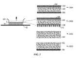
- FIG. 3is a side view of polymerizable material 34 between substrate 12 and porous template 300 , along with enlarged cross-sectional views of various porous template embodiments for use in nano-imprint lithography.
- the arrowindicates the direction of gas transport into template 300 .
- Template 300 Aincludes a porous layer 302 between base layer 304 and cap layer 306 .
- Porous layer 302may be formed by chemical vapor deposition (CVD), spin-coating, thermal growth methods, or the like on base layer 304 .
- a thickness of porous layer 302may be at least about 10 nm.
- a thickness of porous layer 302may be in a range of about 10 nm to about 100 ⁇ m, or in a range of about 100 nm to about 10 ⁇ m.
- a thicker porous layer 302may provide higher effective permeability, without significantly reducing performance related to, for example, UV transparency, thermal expansion, etc.
- Porous layer 302may be made from materials including, but not limited to anodized a-alumina; organo-silane, organo-silica, or organosilicate materials; organic polymers; inorganic polymers, and any combination thereof.
- the porous materialmay be low-k, porous low-k, or ultra-low-k dielectric film, such as spin-on glass (SOG) used in electronic and semiconductor applications.
- SOGspin-on glass
- the porous materialmay be selected to withstand repeated use in nano-imprint lithography processes, including Piranha reclaim processes.
- Adhesion of the porous layer 302 to the base layer 304 and the cap layer 306may be, for example, at least about three times the force required to separate the template from the patterned layer formed in an imprint lithography process.
- the porous materialmay be substantially transparent to UV radiation.
- a tensile modulus of the porous materialmay be, for example, at least about 2 GPa, at least about 5 GPa, or at least about 10 GPa.
- porous layers with different pore size and pore densitymay be produced.
- ion bombardmentmay be used to form pores in a material.
- Porous layer 302may have pores 308 with a larger pore size and a greater porosity than fused silica.
- porosityrefers to the fraction, as a percent of total volume, occupied by channels and open spaces in a solid.
- the porosity of porous layer 302may range from about 0.1% to about 60%, or from about 5% to about 45%. In some cases, the porosity of porous layer 302 may be at least about 10% or at least about 20%.
- the relative porosity of similar materialsmay be defined as a relative difference in density of the materials.
- Fused silicamay be used as a reference material for other materials including oxygen-silicon bonds.
- a relative porosity of a porous material including oxygen-silicon bonds with respect to fused silicais at least about 10%, at least about 20%, or at least about 30%.
- Sizes of the pores in a porous materialmay be well-controlled (e.g., substantially uniform, or with a desired distribution).
- a pore size or average pore sizeis less than about 10 nm, less than about 3 nm, or less than about 1 nm.
- the pore size or average pore sizeis at least about 0.4 nm, at least about 0.5 nm, or larger. That is, the pore size or average pore size may be large enough to provide a sufficient number of solubility sites for a gas, such that the gas, when trapped between the substrate/imprinting stack and the template 300 A, is able to diffuse into porous layer 302 of the template.
- Silsesquioxane polymersare exemplary porous materials.
- “Highly Porous Polyhedral Silsesquioxane Polymers. Synthesis and Characterization,” J. Am. Chem. Soc., 1998, 120, 8380-8391, which is hereby incorporated by reference herein, Zhang et al.describe small intracube pores and larger intercube pores in silsesquioxane polymers.
- the intracube poresare approximated by a 0.3-0.4 nm sphere.
- the intercube poresare oblong with a 0.5-0.6 nm diameter and a length of 1.0-1.2 nm.
- pores with a diameter of at least about 0.4 nmare believed to provide solubility sites of a size and shape suitable to absorb gases with a kinetic diameter smaller than the dimensions of the solubility sites.
- the structure of the solubility sites of a porous materialmay allow the absorbed gas to be substantially held in the solubility sites, rather than diffusing out of the material.
- Porogensmay be added to material used to form porous layer 302 to increase the porosity and pore size of the porous layer.
- Porogensinclude, for example, organic compounds that may be vaporized, such as norbornene, ⁇ -terpinene, polyethylene oxide, and polyethylene oxide/polypropylene oxide copolymer, and the like, and any combination thereof.
- Porogensmay be, for example, linear or star-shaped.
- Porogens and process conditionsmay be selected to form a microporous low-k porous layer, for example, with an average pore diameter of less than about 2 nm, thereby increasing the number of solubility sites for a range of gases.
- porogens and the increased porositymay enlarge the structure channels connecting gas solubility sites.
- helium permeability of a low-k filmmay exceed helium permeability of vitreous fused silica.
- Base layer 304 and cap layer 306may be made of the same or different material.
- base layer 304may be fused silica and cap layer 306 may include SiO x , with 1 ⁇ x ⁇ 2, grown through a vapor deposition method.
- a thickness and composition of cap layer 306may be chosen to provide mechanical strength and selected surface properties, as well as permeability to gases that may be trapped between a substrate/imprinting stack and a template in an imprint lithography process.
- a thickness of cap layer 306is less than about 100 nm, less than about 50 nm, or less than about 20 nm. In an example, cap layer 306 is about 10 nm thick.
- Cap layer 306may be formed by material selected to achieve desirable wetting and release performance during an imprint lithography process. Cap layer 306 may also inhibit penetration of polymerizable material 34 into the porous layer while allowing gas to diffuse through the cap layer and into the porous layer 302 .
- effective permeabilitymay be calculated from a resistance model, such as an analog of an electric circuit described by F. Peng, et al. in J. Membrane Sci. 222 (2003) 225-234 and A. Ranjit Prakash et al. in Sensors and Actuators B 113 (2006) 398-409, which are both hereby incorporated by reference herein.
- the resistance of a material to the permeation of a vaporis defined as the permeance resistance, R p .
- permeance resistancemay be defined as:
- equation (2)may be rewritten as:
- template permeabilitymay be adjusted by selecting porosity and pore size of the porous layer 302 .
- the effect of the permeability and thickness of porous layer 302 on the effective permeability of a multi-layer composite imprinting stack with a thickness of 310 nmis shown in Table 2.
- Table 2suggests that increasing a thickness of the porous layer alone may yield a higher effective permeability than increasing the permeability of the porous layer alone. That is, for a porous layer thickness of 300 nm and a cap layer thickness of 10 nm, a ten-fold increase in permeability of the porous layer from 100P 1 to 1000P 1 increases the effective permeability from 23.8P 1 to 30.1P 1 . For composite imprinting stacks with a porous layer thickness of 100 nm, 200 nm, and 300 nm and a cap layer thickness of 10 nm, the effective permeability increases twenty-fold, from 1.5P 1 to 2.8P 1 to 30.1P 1 , respectively, over the 200 nm increase in porous layer thickness.
- protrusions 310may extend from cap layer 306 .
- template 300 Bmay be formed by depositing a 500 nm thick porous layer (e.g., an organosilicate low-k film) on a base layer (e.g., quartz), and growing a 100 nm thick cap layer (e.g., SiO x ) on top of the porous layer. The cap layer is etched back to form protrusions 90 nm in height.
- a thickness of cap layer 306is considered independently of the height of the protrusions 310 .
- the cap layer in this exampleis considered to be 10 nm thick, with protrusions 90 nm in height extending from the cap layer.
- At least about 50% of the template surfacehas a 10 nm thick covering of SiO x (i.e., about 50% of the template surface area is covered with protrusions) with a 500 nm thick porous layer underneath.
- Heliummay diffuse more quickly through portions of the cap layer from which there are no protrusions, achieving an overall increase in helium permeability at least partially dependent on the thickness of the porous layer, the thickness of the cap layer, and the fraction of the surface area of the template free from protrusions.
- a templatemay be formed as a unitary structure with a porosity and average pore size selected to allow diffusion of a gas. Templates made from, for example, organic polymers, inorganic materials (e.g., silicon carbide, doped silica, VYCOR®), and the like, or any combination thereof, may have a lower packing density, and therefore a higher gas (e.g., helium) permeability, than vitreous fused silica.
- FIG. 3illustrates template 300 C. Template 300 C consists essentially of a single porous layer 302 . The porous layer 302 is not adhered to a base layer. The porous layer may have an average pore size of at least about 0.4 nm and a porosity of at least about 10%.
- Template 300 Dincludes porous layer 302 with a cap layer 306 .
- Cap layer 306may be, for example, SiO x .
- the porous layeris not adhered to a base layer.
- the cap layer 306may inhibit penetration of the polymerizable material into the porous material.
- the cap layer 306may also impart desirable surface properties, mechanical properties, and the like to the template.
- An imprinting stackmay include a substrate and a layer adhered to the substrate.
- Multi-layer imprinting stacksmay include one or more additional layers adhered together to form a multi-layer composite.
- the substratemay be, for example, a silicon wafer.
- a layer adhered to the substratemay include, for example, organic polymeric material, inorganic polymeric material, or any combination thereof. Pore size and porosity of the substrate, the layers, or any combination thereof may be selected to allow diffusion of a gas through the imprinting stack, thus facilitating reduction of trapped gases and filling of features in the template during an imprint lithography process.
- FIG. 4illustrates polymerizable material 34 between template 18 and imprinting stack 400 .
- the arrowindicates the direction of gas transport into the imprinting stack.
- gas permeability of the imprinting stack 400may be increased by increasing a thickness of the imprinting stack.
- increasing a thickness of the imprinting stackmay improve the gas absorption capacity of the stack, and reduce the probability of gas saturation during a purge.
- the imprinting stackmay include a porous layer 402 formed on substrate 12 .
- Porous layer 402may have pores 408 and may be, for example, an organosilicate low-k film.
- Cap layer 406may be formed on porous layer 402 .
- a thickness of porous layer 402may be in a range of about 50 nm to a few ⁇ m, depending on the intended use. Pore size in the porous layer may be well-controlled (e.g., substantially uniform or with a known distribution).
- a pore size or average pore size of porous layer 402is less than about 10 nm, less than about 3 nm, or less than about 1 nm. In some cases, the pore size or average pore size is at least about 0.4 nm, at least about 0.5 nm, or larger. That is, the pore size or average pore size may be large enough to provide a sufficient number of solubility sites for a gas (e.g., helium), such that gas trapped between the substrate 12 and a template 18 may diffuse into porous layer 402 of the imprinting stack 400 . In some embodiments, a porosity of porous layer 402 is at least 10% or at least 20%.
- a gase.g., helium
- strain from the base layer of a porous template or from the substrate of a porous imprinting stackmay be transferred through the porous layer to the cap layer.
- the porous layermay have a lower Young's modulus than the base layer or substrate.
- transfer of the strainmay be reduced by embedding porous material in the substrate. For example, a multiplicity of recesses or grooves may be etched into a substrate or base layer, porous material may be deposited in the recesses or grooves. In some cases, the porous material may substantially fill the recesses or grooves.
- a cap layermay be deposited on the base layer or substrate to substantially cover the base layer or substrate and the porous material, such that the cap layer is in contact with the base layer or substrate, and strain transfer is reduced.
- the area and spacing of the recesses or grooves, and the volume of the porous materialmay be sufficient to allow gas to escape into the porous material during an imprint lithography process.
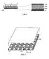
- FIG. 5illustrates an exploded perspective view of layer 500 with recesses 502 .
- Layer 500may be, for example, a substrate.
- Recesses 502may include, for example, grooves or depressions of any regular or irregular, uniform or non-uniform shape or size. In some embodiments, recesses 502 may form a grid pattern with uniform or non-uniform spacings. Grid spacing a may be, for example, about 0.25 ⁇ m.
- Recesses 502may be substantially filled with porous material 504 .
- a cap layer 506may be formed over layer 500 and porous material 504 in recesses 502 , such that strain may be transferred directly from the layer 500 to the cap layer 506 , while still allowing increased diffusion of gas through the template 500 .
- the cap layer 506may be formed by methods including, for example, chemical vapor deposition and the like.
- the time required for drops of a polymerizable material to form a substantially continuous layer between the imprinting stack/substrate and the templatemay be at most about 80%, at most about 50%, or at most about 20%, of the time required for the same arrangement of drops of the same polymerizable material to form a substantially continuous layer between a similar imprinting stack/substrate and a second template when the second template is less porous, or has a lower porosity, than the porous template (e.g., when the second template is made of fused silica, quartz, or common template material).
- the time required for drops of a polymerizable material to form a substantially continuous layer between the imprinting stack/substrate and the templatemay be at most about 80%, at most about 50%, or at most about 20%, of the time required for the same arrangement of drops of the same polymerizable material to form a substantially continuous layer between a second imprinting stack/substrate and a similar template when the second imprinting stack/substrate is less porous, or has a lower porosity, than the porous imprinting stack/substrate (e.g., when the second imprinting stack consists essentially of an adhesion layer on a silicon wafer).
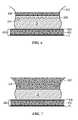
- a porous template and a porous imprinting stackmay be used together.
- a porous layer 302may be included in the template 300
- porous layer 402may be included in the imprinting stack 400 .
- Introducing a porous layer in both the template and the imprinting stackmay allow an increased amount of gas (e.g., helium, nitrogen, oxygen, etc.) to escape through the porous layers if, for example, the cap layers are sufficiently thin.
- gase.g., helium, nitrogen, oxygen, etc.
- FIG. 7a unitary porous template 300 and an imprinting stack with a porous layer may be used together.
- SOGSpin-On-Glass, ACCUGLASS® 512B, available from Honeywell Electronic Materials
- the waferwas then baked at 80° C., 150° C. and 250° C., respectively, for 60-120 seconds at each temperature.
- the SOG-coated waferwas then cured at 425° C.-450° C. in a nitrogen environment for 1 hour.
- the SOG layerwas about 1.7 ⁇ m thick.
- the resulting hydrophobic SOG surfacewas treated with oxygen plasma for 5-20 seconds to generate a hydrophilic surface.
- An adhesion layerwas formed on the SOG surface from a composition including approximately 77 grams of IsoRad 501 (a multi-functional reactive compound available from Schenectady International, Inc. in Schenectady, N.Y.), 22 grams of Cymel 303ULF (a cross-linking agent including hexamethoxymethyl-melamine (HMMM), available from Cytec Industries, Inc. of West Patterson, N.J.) and 1 gram of Cycat 4040 (a catalyst available from Cytec Industries, Inc.), and approximately 39.9 kilograms of PM Acetate (a solvent including 2-(1-methoxy) propyl acetate, available from Eastman Chemical Company, Kingsport, Tenn.). The composition was spun on the SOG layer and cured at 160° C. for 60 seconds to form an adhesion layer with a thickness of about 7 nm.
- IsoRad 501a multi-functional reactive compound available from Schenectady International, Inc. in Schenectady, N.Y.
- SOGSpin-On-Glass, ACCUGLASS® 512B, by Honeywell Electronic Materials
- the templatewas then baked at 80° C., 150° C. and 250° C., respectively, for 60-120 seconds at each temperature.
- the SOG-coated templatewas then cured at 425° C.-450° C. in a nitrogen environment for 1 hour.
- the SOG layerwas about 650 ⁇ m thick.
- the templatewas cleaned with standard wet cleaning process.
- a silicon oxide cap layerwas deposited using plasma-enhanced chemical vapor deposition (PEVCD). The cap layer was about 8 nm thick.
- PEVCDplasma-enhanced chemical vapor deposition
- Imprint resists similar to bulk material A8e.g., viscosity about 10 cP
- U.S. Pat. No. 7,307,118which is hereby incorporated by reference herein, were used to test filling speeds for porous imprinting stacks made as described above.
- the imprint resistwas dispensed in a grid pattern on the imprinting stack as shown in FIG. 8 , with drops 800 of imprint resist spaced 340 ⁇ m center-to-center and a drop volume of about 12 pL. Interstitial regions 802 are visible between drops 800 .
- a helium purgewas performed to substantially replace air between the imprinting stack and the template with helium.
- the residual layer thickness of the solidified resistwas about 90 nm in each case.
- FIG. 9Ais a photograph of drops 900 of imprint resist between an imprinting stack and a blank fused silica template at the time the template contacts the imprint resist. Interstitial regions 902 cover more surface area than the drops 900 .
- FIG. 9Bis a photograph taken 1 second after contact of the imprint resist with the template. The field of view of the camera has been adjusted such that four interstitial regions 902 are visible.
- FIG. 9Cis a photograph taken 7 seconds after contact of the imprint resist with the template. Two interstitial regions 902 are visible.
- FIG. 9Dshows complete spreading of the imprint resist to form a substantially continuous layer 904 between the template and the imprinting stack 8 seconds after the template contacted the imprint resist.
- FIG. 10Ais a photograph of drops 1000 of imprint resist between a porous imprinting stack and a blank fused silica template at the time the template contacts the imprint resist.
- the porous imprinting stackincludes a silicon wafer coated with a SOG layer with a thickness of about 1.7 ⁇ m, and an 8 nm adhesion layer over the SOG layer, as described above.
- FIG. 10Bis a photograph taken 0.5 seconds after contact of the imprint resist with the template. The field of view of the camera has been adjusted such that four interstitial regions 1002 are visible.
- FIG. 10Cis a photograph taken 0.75 seconds after contact of the imprint resist with the template. Three interstitial regions 1002 are visible.
- FIG. 10Dshows complete spreading of the imprint resist to form a substantially continuous layer 1004 between the template and the porous imprinting stack 1.1 seconds after the template contacted the imprint resist.
Landscapes
- Engineering & Computer Science (AREA)
- Nanotechnology (AREA)
- Chemical & Material Sciences (AREA)
- Physics & Mathematics (AREA)
- Crystallography & Structural Chemistry (AREA)
- General Physics & Mathematics (AREA)
- Condensed Matter Physics & Semiconductors (AREA)
- Manufacturing & Machinery (AREA)
- Mathematical Physics (AREA)
- Theoretical Computer Science (AREA)
- Shaping Of Tube Ends By Bending Or Straightening (AREA)
- Exposure Of Semiconductors, Excluding Electron Or Ion Beam Exposure (AREA)
- Printing Plates And Materials Therefor (AREA)
- Moulds For Moulding Plastics Or The Like (AREA)
- Micromachines (AREA)
Abstract
Description
- This application claims the benefit under 35 U.S.C. §119(e)(1) of U.S. provisional application 60/989,681, filed Nov. 21, 2007, and U.S. provisional application 60/991,954 filed Dec. 3, 2007, both of which are hereby incorporated by reference herein.
- The United States government has a paid-up license in this invention and the right in limited circumstance to require the patent owner to license others on reasonable terms as provided by the terms of NIST ATP AWARD 70NANB4H3012.
- Nano-fabrication includes the fabrication of very small structures that have features on the order of 100 nanometers or smaller. One application in which nano-fabrication has had a sizeable impact is in the processing of integrated circuits. The semiconductor processing industry continues to strive for larger production yields while increasing the circuits per unit area formed on a substrate, therefore nano-fabrication becomes increasingly important. Nano-fabrication provides greater process control while allowing continued reduction of the minimum feature dimensions of the structures formed. Other areas of development in which nano-fabrication has been employed include biotechnology, optical technology, mechanical systems, and the like.
- In one aspect, an imprint lithography template or imprinting stack includes a porous material defining a multiplicity of pores with an average pore size of at least about 0.4 nm. A porosity of the porous material is at least about 10%.
- In some implementations, the average pore size is at least about 0.5 nm or at least about 1.0 nm. The porosity of the porous material may be at least about 20%. In some cases, the porous material is an organosilicate low-k material. The relative porosity of the porous material with respect to fused silica may be at least about 20%. In some cases, the porous material has a Young's modulus of at least about 2 GPa, at least about 5 GPa, or at least about 10 GPa.
- In some template implementations, the porous material is positioned between a base layer and a cap layer. The base layer may include fused silica. In some cases, the base layer includes recesses, and the porous material is positioned in the recesses. In some cases, the cap layer includes SiOx, with 1≦x≦2. A thickness of the cap layer maybe less than about 100 nm, less than about 50 nm, or less than about 20 nm. Protrusions may extend from the cap layer.
- In some imprinting stack implementations, the porous material is positioned between a substrate and a cap layer. The substrate may include silicon.
- In another aspect, forming an imprint lithography template includes forming a porous layer on a base layer, and forming a cap layer on the porous layer. In another aspect, forming an imprint lithography template includes forming a multiplicity of recesses in a base, depositing a porous material in the recesses, and forming a cap layer on the base layer. In another aspect, forming an imprint lithography stack includes forming a porous layer on a substrate, and forming a cap layer on the porous layer. The porous layer defines a multiplicity of pores with an average pore size of at least about 0.4 nm, and the porosity of the porous layer is at least about 10%.
- In another aspect, an imprint lithography method includes applying drops of a polymerizable material to an imprinting stack, contacting the polymerizable material with a template, solidifying the polymerizable material, and separating the template from the solidified material. In some cases, the template includes a porous material. In some cases, the imprinting stack includes a porous material. In some cases, the template and the imprinting stack both include a porous material. The porous material defines a multiplicity of pores with an average pore size of at least about 0.4 nm, and the porosity of the porous material is at least about 10%.
- In another aspect, an imprint lithography method includes dispensing drops of a polymerizable material on a surface of an imprinting stack, contacting the polymerizable material with a template, and allowing the polymerizable material to spread to form a substantially continuous layer on the surface of the imprinting stack. The template, the imprinting stack, or both may include a porous material defining a multiplicity of pores with an average pore size of at least about 0.4 nm, and the porosity of the porous material is at least about 10%. Spreading of the polymerizable material to form the substantially continuous layer occurs in about 80% or less, about 50% or less, or about 20% less of the time required for a similar distribution of a similar polymerizable material to form a substantially continuous layer between a second template and a second imprinting stack, where the second template and the second imprinting stack have an average pore size of less than about 0.4 nm.
- So that the present invention may be understood in more detail, a description of embodiments of the invention is provided with reference to the embodiments illustrated in the appended drawings. It is to be noted, however, that the appended drawings illustrate only typical embodiments of the invention, and are therefore not to be considered limiting of the scope.
FIG. 1 illustrates a simplified side view of a lithographic system.FIG. 2 illustrates a simplified side view of the substrate shown inFIG. 1 having a patterned layer positioned thereon.FIG. 3 illustrates porous templates.FIG. 4 illustrates a porous imprinting stack.FIG. 5 illustrates a portion of a layer with porous material in a multiplicity of recesses.FIG. 6 illustrates an imprint lithography process using a porous template and a porous imprinting stack.FIG. 7 illustrates an imprint lithography process using a unitary porous template and a porous imprinting stack.FIG. 8 . is a photograph of drops of imprint resist as dispensed on a substrate.FIGS. 9A-D are photographs of drops of imprint resist spreading on an imprinting stack.FIGS. 10A-D are photographs of drops of imprint resist spreading on a porous imprinting stack.- An exemplary nano-fabrication technique in use today is commonly referred to as imprint lithography. Exemplary imprint lithography processes are described in detail in numerous publications, such as U.S. Patent Application Publication No. 2004/0065976, U.S. Patent Application Publication No. 2004/0065252, and U.S. Pat. No. 6,936,194, all of which are hereby incorporated by reference herein.
- An imprint lithography technique disclosed in each of the aforementioned U.S. patent application publications and patent includes formation of a relief pattern in a formable (polymerizable) layer and transferring a pattern corresponding to the relief pattern into an underlying substrate. The substrate may be coupled to a motion stage to facilitate positioning for the patterning process. The patterning process uses a template spaced apart from the substrate and the formable liquid applied between the template and the substrate. The formable liquid is solidified to form a rigid layer that has a pattern conforming to a shape of the surface of the template that contacts the formable liquid. After solidification, the template is separated from the rigid layer such that the template and the substrate are spaced apart. The substrate and the solidified layer are then subjected to additional processes to transfer a relief image into the substrate that corresponds to the pattern in the solidified layer.
- Referring to
FIG. 1 , illustrated therein is alithographic system 10 used to form a relief pattern onsubstrate 12. An imprint lithography stack may includesubstrate 12 and one or more layers (e.g., an adhesion layer) adhered to the substrate.Substrate 12 may be coupled tosubstrate chuck 14. As illustrated,substrate chuck 14 is a vacuum chuck.Substrate chuck 14, however, may be any chuck including, but not limited to, vacuum, pin-type, groove-type, electromagnetic, and the like, or any combination thereof. Exemplary chucks are described in U.S. Pat. No. 6,873,087, which is hereby incorporated by reference herein. Substrate 12 andsubstrate chuck 14 may be further supported bystage 16.Stage 16 may provide motion about the x-, y-, and z-axes.Stage 16,substrate 12, andsubstrate chuck 14 may also be positioned on a base (not shown).- Spaced-apart from
substrate 12 is atemplate 18.Template 18 may include amesa 20 extending therefrom towardssubstrate 12,mesa 20 having apatterning surface 22 thereon. Further,mesa 20 may be referred to asmold 20.Template 18 and/ormold 20 may be formed from such materials including, but not limited to, fused-silica, quartz, silicon, organic polymers, siloxane polymers, borosilicate glass, fluorocarbon polymers, metal, hardened sapphire, and the like, or any combination thereof. As illustrated, patterningsurface 22 comprises features defined by a plurality of spaced-apart recesses24 and/orprotrusions 26, though embodiments of the present invention are not limited to such configurations. Patterningsurface 22 may define any original pattern that forms the basis of a pattern to be formed onsubstrate 12. Template 18 may be coupled to chuck28.Chuck 28 may be configured as, but not limited to, vacuum, pin-type, groove-type, electromagnetic, and/or other similar chuck types. Exemplary chucks are further described in U.S. Pat. No. 6,873,087, which is hereby incorporated by reference herein. Further, chuck28 may be coupled toimprint head 30 such thatchuck 28 and/orimprint head 30 may be configured to facilitate movement oftemplate 18.System 10 may further comprise a fluid dispensesystem 32. Fluid dispensesystem 32 may be used to depositpolymerizable material 34 onsubstrate 12.Polymerizable material 34 may be positioned uponsubstrate 12 using techniques such as drop dispense, spin-coating, dip coating, chemical vapor deposition (CVD), physical vapor deposition (PVD), thin film deposition, thick film deposition, and the like, or any combination thereof. Polymerizable material34 (e.g., imprint resist) may be disposed uponsubstrate 12 before and/or after a desired volume is defined betweenmold 20 andsubstrate 12 depending on design considerations.Polymerizable material 34 may include components as described in U.S. Pat. No. 7,157,036 and U.S. Patent Application Publication No. 2005/0187339, both of which are hereby incorporated by reference herein.- Referring to
FIGS. 1 and 2 ,system 10 may further comprise anenergy source 38 coupled todirect energy 40 alongpath 42.Imprint head 30 andstage 16 may be configured to positiontemplate 18 andsubstrate 12 in superimposition withpath 42.System 10 may be regulated by aprocessor 54 in communication withstage 16,imprint head 30, fluid dispensesystem 32,source 38, or any combination thereof, and may operate on a computer readable program stored inmemory 56. - Either
imprint head 30,stage 16, or both may alter a distance betweenmold 20 andsubstrate 12 to define a desired volume therebetween that is substantially filled bypolymerizable material 34. For example,imprint head 30 may apply a force totemplate 18 such thatmold 20 contactspolymerizable material 34. After the desired volume is substantially filled withpolymerizable material 34,source 38 producesenergy 40, e.g., broadband ultraviolet radiation, causingpolymerizable material 34 to solidify and/or cross-link conforming to shape of asurface 44 ofsubstrate 12 andpatterning surface 22, defining apatterned layer 46 onsubstrate 12.Patterned layer 46 may include aresidual layer 48 and a plurality of features shown asprotrusions 50 andrecessions 52, withprotrusions 50 having a thickness t1andresidual layer 48 having a thickness t2. - The above-described system and process may be further implemented in imprint lithography processes and systems referred to in U.S. Pat. No. 6,932,934, U.S. Patent Application Publication No. 2004/0124566, U.S. Patent Application Publication No. 2004/0188381, and U.S. Patent Application Publication No. 2004/0211754, each of which is hereby incorporated by reference herein.
- In nano-imprint processes in which polymerizable material is applied to a substrate by drop dispense or spin coating methods, gases may be trapped inside recesses in the template after the template contacts the polymerizable material. In nano-imprint processes in which polymerizable material is applied to a substrate by drop dispense methods, gases may also be trapped between drops of polymerizable material or imprint resist dispensed on a substrate or on an imprinting stack. That is, gases may be trapped in interstitial regions between drops as the drops spread.
- Gas escape and dissolution rates may limit the rate at which the polymerizable material is able to form a continuous layer on the substrate (or imprinting stack) or the rate at which the polymerizable material is able to fill template features after the template contacts the polymerizable material, thereby limiting throughput in nano-imprint processes. For example, a substrate or a template may be substantially impermeable to a gas trapped between the substrate and the template. In some cases, a polymeric layer adhered to the substrate or the template may become saturated with gas, such that gas between the imprinting stack and the template is substantially unable to enter the saturated polymeric layer, and remains trapped between the substrate and the substrate or imprinting stack. Gas that remains trapped between the substrate or the imprinting stack and the template may cause filling defects in the patterned layer.
- In an imprint lithography process, gas trapped between the substrate/imprinting stack and the template may escape through the polymerizable material, the substrate/imprinting stack, the template, or any combination thereof. The amount of gas that escapes through any medium may be influenced by the contact area between the trapped gas and the medium. The contact area between the trapped gas and the polymerizable material may be less than the contact area between the trapped gas and the substrate/imprinting stack and less than the contact area between the trapped gas and the template. For example, a thickness of the polymerizable material on a substrate/imprinting stack may be less than about 1 μm, or less than about 100 nm. In some cases, a polymerizable material may absorb enough gas to become saturated with the gas before imprinting, such that trapped gas is substantially unable to enter the polymerizable material. In contrast, the contact area between the trapped gas and the substrate or imprinting stack, or the contact area between the trapped gas and the template, may be relatively large.
- In some cases, the substrate/imprinting stack or template may include a porous material defining a multiplicity of pores with an average pore size and pore density or relative porosity selected to facilitate diffusion of a gas into the substrate/imprinting stack or the template, respectively. In certain cases, the substrate/imprinting stack or template may include one or more layers or regions of a porous material designed to facilitate transport of gases trapped between the substrate/imprinting stack and the template in a direction away from the polymerizable material between the substrate/imprinting stack and substrate and toward the substrate/imprinting stack or the template, respectively.
- The gas permeability of a medium may be expressed as P=D×S, in which P is the permeability, D is the diffusion coefficient, and S is the solubility. In a gas transport process, a gas adsorbs onto a surface of the medium, and a concentration gradient is established within the medium. The concentration gradient may serve as the driving force for diffusion of gas through the medium. Gas solubility and the diffusion coefficient may vary based on, for example, packing density of the medium. Adjusting a packing density of the medium may alter the diffusion coefficient and hence the permeability of the medium.
- A gas may be thought of as having an associated kinetic diameter. The kinetic diameter provides an idea of the size of the gas atoms or molecules for gas transport properties. D. W. Breck, Zeolite Molecular Sieves—Structure, Chemistry, and Use, John Wiley & Sons, New York, 1974, p. 636, which is hereby incorporated by reference herein) lists the kinetic diameter for helium (0.256 nm), argon (0.341 nm), oxygen (0.346 nm), nitrogen (0.364 nm), and other common gases.
- In some imprint lithography processes, a helium purge is used to substantially replace air between the template and the substrate or imprinting stack with helium gas. To simplify the comparison between a helium environment and an air environment in an imprint lithography process, the polar interaction between oxygen in air and silica may be disregarded by modeling air as pure argon. Both helium and argon are inert gases, and argon has a kinetic diameter similar to that of oxygen. Unlike oxygen, however, helium and argon do not interact chemically with fused silica or quartz (e.g., in a template or substrate).
- Internal cavities (solubility sites) and structural channels connecting the solubility sites allow a gas to permeate through a medium. The gas may be retained in the solubility sites. The size of the internal cavities and the channel diameter relative to the size (or kinetic diameter) of the gas influence the rate at which the gas permeates the medium.
- The sizes of individual interstitial solubility sites of fused silica have been shown to follow a log-normal distribution by J. F. Shackelford in J. Non-Cryst. Solids 253, 1999, 23, which is hereby incorporated by reference herein. As indicated by the interstitial diameter distribution (mode=0.181 nm; mean=0.196 nm) and the kinetic diameter of helium and argon, the number of fused silica solubility sites available to helium exceeds the number of solubility sites available to argon. The total number of interstitial sites is estimated to be 2.2×1028per m3, with 2.3×1027helium solubility sites per m3and 1.1×1026argon solubility sites per m3. The average distance between solubility sites for helium is considered to be 0.94 nm, while the average distance between solubility sites for argon is considered to be 2.6 nm. The structural channels connecting these solubility sites are thought to be similar to the helical arrangement of 6-member Si—O rings, with a diameter of about 0.3 nm. Table 1 summarizes some parameters affecting helium and argon permeability in fused silica.
TABLE 1 Helium Argon Kinetic Diameter (nm) 0.256 0.341 Solubility Site Density (m−3) 2.3 × 1027 1.1 × 1026 Distant Between Solubility Sites (nm) 0.94 2.6 Structural Channel Diameter Connecting ~0.3 ~0.3 Solubility Sites (nm) - Boiko (G. G. Boiko, etc., Glass Physics and Chemistry, Vol. 29, No. 1, 2003, pp. 42-48, which is hereby incorporated by reference herein) describes behavior of helium in amorphous or vitreous silica. Within a solubility site, the helium atom vibrates at an amplitude allowed by the interstitial volume. The atom passes from interstice to interstice through channels, which may be smaller in diameter than the interstices.
- The parameters listed in Table 1 indicate that argon permeability in fused silica may be very low or negligible at room temperature (i.e., the kinetic diameter of argon exceeds the fused silica channel size). Since the kinetic diameters of oxygen and nitrogen are larger than the kinetic diameter of argon, air may be substantially unable to permeate fused silica. On the other hand, helium may diffuse into and permeate fused silica. Thus, when a helium environment is used rather than ambient air for a nano-imprint process, helium trapped between the template and the substrate or imprinting stack may be able to permeate a fused silica template.
FIG. 3 is a side view ofpolymerizable material 34 betweensubstrate 12 andporous template 300, along with enlarged cross-sectional views of various porous template embodiments for use in nano-imprint lithography. The arrow indicates the direction of gas transport intotemplate 300.Template 300A includes aporous layer 302 betweenbase layer 304 andcap layer 306.Porous layer 302 may be formed by chemical vapor deposition (CVD), spin-coating, thermal growth methods, or the like onbase layer 304. A thickness ofporous layer 302 may be at least about 10 nm. For example, a thickness ofporous layer 302 may be in a range of about 10 nm to about 100 μm, or in a range of about 100 nm to about 10 μm. In some cases, a thickerporous layer 302 may provide higher effective permeability, without significantly reducing performance related to, for example, UV transparency, thermal expansion, etc.Porous layer 302 may be made from materials including, but not limited to anodized a-alumina; organo-silane, organo-silica, or organosilicate materials; organic polymers; inorganic polymers, and any combination thereof. In some embodiments, the porous material may be low-k, porous low-k, or ultra-low-k dielectric film, such as spin-on glass (SOG) used in electronic and semiconductor applications. The porous material may be selected to withstand repeated use in nano-imprint lithography processes, including Piranha reclaim processes. Adhesion of theporous layer 302 to thebase layer 304 and thecap layer 306 may be, for example, at least about three times the force required to separate the template from the patterned layer formed in an imprint lithography process. In some embodiments, the porous material may be substantially transparent to UV radiation. A tensile modulus of the porous material may be, for example, at least about 2 GPa, at least about 5 GPa, or at least about 10 GPa.- By varying the process conditions and materials, porous layers with different pore size and pore density (e.g., porosity or relative porosity) may be produced. In some cases, for example, ion bombardment may be used to form pores in a material.
Porous layer 302 may havepores 308 with a larger pore size and a greater porosity than fused silica. As used herein, “porosity” refers to the fraction, as a percent of total volume, occupied by channels and open spaces in a solid. The porosity ofporous layer 302 may range from about 0.1% to about 60%, or from about 5% to about 45%. In some cases, the porosity ofporous layer 302 may be at least about 10% or at least about 20%. The relative porosity of similar materials may be defined as a relative difference in density of the materials. For example, a relative porosity of SOG (density ρSOG=1.4 g/cm3) with respect to fused silica (density ρfused silica=2.2 g/cm3) may be calculated as 100%×(ρfused silica−ρSOG)/ρfused silica, or 36%. Fused silica may be used as a reference material for other materials including oxygen-silicon bonds. In some embodiments, a relative porosity of a porous material including oxygen-silicon bonds with respect to fused silica is at least about 10%, at least about 20%, or at least about 30%. - Sizes of the pores in a porous material may be well-controlled (e.g., substantially uniform, or with a desired distribution). In some cases, a pore size or average pore size is less than about 10 nm, less than about 3 nm, or less than about 1 nm. In some cases, the pore size or average pore size is at least about 0.4 nm, at least about 0.5 nm, or larger. That is, the pore size or average pore size may be large enough to provide a sufficient number of solubility sites for a gas, such that the gas, when trapped between the substrate/imprinting stack and the
template 300A, is able to diffuse intoporous layer 302 of the template. - Silsesquioxane polymers are exemplary porous materials. In “Highly Porous Polyhedral Silsesquioxane Polymers. Synthesis and Characterization,” J. Am. Chem. Soc., 1998, 120, 8380-8391, which is hereby incorporated by reference herein, Zhang et al. describe small intracube pores and larger intercube pores in silsesquioxane polymers. The intracube pores are approximated by a 0.3-0.4 nm sphere. The intercube pores are oblong with a 0.5-0.6 nm diameter and a length of 1.0-1.2 nm. As discussed herein, pores with a diameter of at least about 0.4 nm, such as silsesquioxane polymers, are believed to provide solubility sites of a size and shape suitable to absorb gases with a kinetic diameter smaller than the dimensions of the solubility sites. In some cases, the structure of the solubility sites of a porous material may allow the absorbed gas to be substantially held in the solubility sites, rather than diffusing out of the material.
- Porogens may be added to material used to form
porous layer 302 to increase the porosity and pore size of the porous layer. Porogens include, for example, organic compounds that may be vaporized, such as norbornene, α-terpinene, polyethylene oxide, and polyethylene oxide/polypropylene oxide copolymer, and the like, and any combination thereof. Porogens may be, for example, linear or star-shaped. Porogens and process conditions may be selected to form a microporous low-k porous layer, for example, with an average pore diameter of less than about 2 nm, thereby increasing the number of solubility sites for a range of gases. In addition, the introduction of porogens and the increased porosity may enlarge the structure channels connecting gas solubility sites. For pore sizes of about 0.4 nm or greater, helium permeability of a low-k film may exceed helium permeability of vitreous fused silica. Base layer 304 andcap layer 306 may be made of the same or different material. In some embodiments,base layer 304 may be fused silica andcap layer 306 may include SiOx, with 1≦x≦2, grown through a vapor deposition method. A thickness and composition ofcap layer 306 may be chosen to provide mechanical strength and selected surface properties, as well as permeability to gases that may be trapped between a substrate/imprinting stack and a template in an imprint lithography process. In some embodiments, a thickness ofcap layer 306 is less than about 100 nm, less than about 50 nm, or less than about 20 nm. In an example,cap layer 306 is about 10 nm thick.Cap layer 306 may be formed by material selected to achieve desirable wetting and release performance during an imprint lithography process.Cap layer 306 may also inhibit penetration ofpolymerizable material 34 into the porous layer while allowing gas to diffuse through the cap layer and into theporous layer 302.- For a multi-layer film, effective permeability may be calculated from a resistance model, such as an analog of an electric circuit described by F. Peng, et al. inJ. Membrane Sci.222 (2003) 225-234 and A. Ranjit Prakash et al. inSensors and ActuatorsB 113 (2006) 398-409, which are both hereby incorporated by reference herein. The resistance of a material to the permeation of a vapor is defined as the permeance resistance, Rp. For a two-layer composite film with layer thicknesses l1and l2, and corresponding permeabilities P1and P2, permeance resistance may be defined as:
- in which □p is the pressure difference across the film, J is the flux, and A is the area. The resistance model predicts
Rp=R1+R2 (2)- When the cross-sectional area is the same for both materials1 and2, equation (2) may be rewritten as:
- For
template 300A withcap layer 306 of SiOxwith a thickness of about 10 nm and permeability P1, template permeability may be adjusted by selecting porosity and pore size of theporous layer 302. The effect of the permeability and thickness ofporous layer 302 on the effective permeability of a multi-layer composite imprinting stack with a thickness of 310 nm is shown in Table 2. TABLE 2 Cap Layer Porous Thickness Layer Base Layer Effective (SiOx), Thickness, Thickness Permeability Permeability Permeability (SiO2), Permeability of the P1 P2 Permeability P1 Ratio Total Stack 10 nm 300 nm 0 P2= 1000 P1 30.1 P 110 nm 200 nm 100 nm P2= 1000 P1 2.8 P 110 nm 100 nm 200 nm P2= 1000 P1 1.5 P 110 nm 300 nm 0 P2= 100 P1 23.8 P1 - Table 2 suggests that increasing a thickness of the porous layer alone may yield a higher effective permeability than increasing the permeability of the porous layer alone. That is, for a porous layer thickness of 300 nm and a cap layer thickness of 10 nm, a ten-fold increase in permeability of the porous layer from 100P1to 1000P1increases the effective permeability from 23.8P1to 30.1P1. For composite imprinting stacks with a porous layer thickness of 100 nm, 200 nm, and 300 nm and a cap layer thickness of 10 nm, the effective permeability increases twenty-fold, from 1.5P1to 2.8P1to 30.1P1, respectively, over the 200 nm increase in porous layer thickness.
- In another embodiment,
protrusions 310 may extend fromcap layer 306. In an example,template 300B may be formed by depositing a 500 nm thick porous layer (e.g., an organosilicate low-k film) on a base layer (e.g., quartz), and growing a 100 nm thick cap layer (e.g., SiOx) on top of the porous layer. The cap layer is etched back to form protrusions 90 nm in height. As used herein, a thickness ofcap layer 306 is considered independently of the height of theprotrusions 310. Thus, the cap layer in this example is considered to be 10 nm thick, with protrusions 90 nm in height extending from the cap layer. At least about 50% of the template surface has a 10 nm thick covering of SiOx(i.e., about 50% of the template surface area is covered with protrusions) with a 500 nm thick porous layer underneath. Helium may diffuse more quickly through portions of the cap layer from which there are no protrusions, achieving an overall increase in helium permeability at least partially dependent on the thickness of the porous layer, the thickness of the cap layer, and the fraction of the surface area of the template free from protrusions. - A template may be formed as a unitary structure with a porosity and average pore size selected to allow diffusion of a gas. Templates made from, for example, organic polymers, inorganic materials (e.g., silicon carbide, doped silica, VYCOR®), and the like, or any combination thereof, may have a lower packing density, and therefore a higher gas (e.g., helium) permeability, than vitreous fused silica.
FIG. 3 illustratestemplate 300C.Template 300C consists essentially of a singleporous layer 302. Theporous layer 302 is not adhered to a base layer. The porous layer may have an average pore size of at least about 0.4 nm and a porosity of at least about 10%. Template 300D includesporous layer 302 with acap layer 306.Cap layer 306 may be, for example, SiOx. As withtemplate 300C, the porous layer is not adhered to a base layer. Thecap layer 306 may inhibit penetration of the polymerizable material into the porous material. Thecap layer 306 may also impart desirable surface properties, mechanical properties, and the like to the template.- An imprinting stack may include a substrate and a layer adhered to the substrate. Multi-layer imprinting stacks may include one or more additional layers adhered together to form a multi-layer composite. The substrate may be, for example, a silicon wafer. A layer adhered to the substrate may include, for example, organic polymeric material, inorganic polymeric material, or any combination thereof. Pore size and porosity of the substrate, the layers, or any combination thereof may be selected to allow diffusion of a gas through the imprinting stack, thus facilitating reduction of trapped gases and filling of features in the template during an imprint lithography process.
FIG. 4 illustratespolymerizable material 34 betweentemplate 18 andimprinting stack 400. The arrow indicates the direction of gas transport into the imprinting stack. In some cases, gas permeability of theimprinting stack 400 may be increased by increasing a thickness of the imprinting stack. In some embodiments, increasing a thickness of the imprinting stack may improve the gas absorption capacity of the stack, and reduce the probability of gas saturation during a purge.- In certain embodiments, as depicted in the enlarged cross-sectional view of
imprinting stack 400, the imprinting stack may include aporous layer 402 formed onsubstrate 12.Porous layer 402 may havepores 408 and may be, for example, an organosilicate low-k film.Cap layer 406 may be formed onporous layer 402. A thickness ofporous layer 402 may be in a range of about 50 nm to a few μm, depending on the intended use. Pore size in the porous layer may be well-controlled (e.g., substantially uniform or with a known distribution). - In some embodiments, a pore size or average pore size of
porous layer 402 is less than about 10 nm, less than about 3 nm, or less than about 1 nm. In some cases, the pore size or average pore size is at least about 0.4 nm, at least about 0.5 nm, or larger. That is, the pore size or average pore size may be large enough to provide a sufficient number of solubility sites for a gas (e.g., helium), such that gas trapped between thesubstrate 12 and atemplate 18 may diffuse intoporous layer 402 of theimprinting stack 400. In some embodiments, a porosity ofporous layer 402 is at least 10% or at least 20%. - In some cases, strain from the base layer of a porous template or from the substrate of a porous imprinting stack may be transferred through the porous layer to the cap layer. The porous layer may have a lower Young's modulus than the base layer or substrate. In certain embodiments, transfer of the strain may be reduced by embedding porous material in the substrate. For example, a multiplicity of recesses or grooves may be etched into a substrate or base layer, porous material may be deposited in the recesses or grooves. In some cases, the porous material may substantially fill the recesses or grooves. Then, a cap layer may be deposited on the base layer or substrate to substantially cover the base layer or substrate and the porous material, such that the cap layer is in contact with the base layer or substrate, and strain transfer is reduced. The area and spacing of the recesses or grooves, and the volume of the porous material may be sufficient to allow gas to escape into the porous material during an imprint lithography process.
FIG. 5 illustrates an exploded perspective view oflayer 500 withrecesses 502.Layer 500 may be, for example, a substrate.Recesses 502 may include, for example, grooves or depressions of any regular or irregular, uniform or non-uniform shape or size. In some embodiments, recesses502 may form a grid pattern with uniform or non-uniform spacings. Grid spacing a may be, for example, about 0.25 μm.Recesses 502 may be substantially filled withporous material 504. A cap layer506 may be formed overlayer 500 andporous material 504 inrecesses 502, such that strain may be transferred directly from thelayer 500 to the cap layer506, while still allowing increased diffusion of gas through thetemplate 500. The cap layer506 may be formed by methods including, for example, chemical vapor deposition and the like.- For an imprint lithography process with a porous template, the time required for drops of a polymerizable material to form a substantially continuous layer between the imprinting stack/substrate and the template may be at most about 80%, at most about 50%, or at most about 20%, of the time required for the same arrangement of drops of the same polymerizable material to form a substantially continuous layer between a similar imprinting stack/substrate and a second template when the second template is less porous, or has a lower porosity, than the porous template (e.g., when the second template is made of fused silica, quartz, or common template material). For an imprint lithography process with a porous imprinting stack/substrate, the time required for drops of a polymerizable material to form a substantially continuous layer between the imprinting stack/substrate and the template may be at most about 80%, at most about 50%, or at most about 20%, of the time required for the same arrangement of drops of the same polymerizable material to form a substantially continuous layer between a second imprinting stack/substrate and a similar template when the second imprinting stack/substrate is less porous, or has a lower porosity, than the porous imprinting stack/substrate (e.g., when the second imprinting stack consists essentially of an adhesion layer on a silicon wafer).
- In some embodiments, as illustrated in
FIG. 6 , a porous template and a porous imprinting stack may be used together. For example, aporous layer 302 may be included in thetemplate 300, andporous layer 402 may be included in theimprinting stack 400. Introducing a porous layer in both the template and the imprinting stack may allow an increased amount of gas (e.g., helium, nitrogen, oxygen, etc.) to escape through the porous layers if, for example, the cap layers are sufficiently thin. In some embodiments, as illustrated inFIG. 7 , a unitaryporous template 300 and an imprinting stack with a porous layer may be used together. - Porous Imprinting Stack Preparation. SOG (Spin-On-Glass, ACCUGLASS® 512B, available from Honeywell Electronic Materials) was spun onto pre-cleaned 8-inch double side polished silicon wafer substrate. The wafer was then baked at 80° C., 150° C. and 250° C., respectively, for 60-120 seconds at each temperature. The SOG-coated wafer was then cured at 425° C.-450° C. in a nitrogen environment for 1 hour. The SOG layer was about 1.7 μm thick. The resulting hydrophobic SOG surface was treated with oxygen plasma for 5-20 seconds to generate a hydrophilic surface.
- An adhesion layer was formed on the SOG surface from a composition including approximately 77 grams of IsoRad 501 (a multi-functional reactive compound available from Schenectady International, Inc. in Schenectady, N.Y.), 22 grams of Cymel 303ULF (a cross-linking agent including hexamethoxymethyl-melamine (HMMM), available from Cytec Industries, Inc. of West Patterson, N.J.) and 1 gram of Cycat 4040 (a catalyst available from Cytec Industries, Inc.), and approximately 39.9 kilograms of PM Acetate (a solvent including 2-(1-methoxy) propyl acetate, available from Eastman Chemical Company, Kingsport, Tenn.). The composition was spun on the SOG layer and cured at 160° C. for 60 seconds to form an adhesion layer with a thickness of about 7 nm.
- Porous Template Preparation. SOG (Spin-On-Glass, ACCUGLASS® 512B, by Honeywell Electronic Materials) was spun onto a pre-cleaned fused silica template. The template was then baked at 80° C., 150° C. and 250° C., respectively, for 60-120 seconds at each temperature. The SOG-coated template was then cured at 425° C.-450° C. in a nitrogen environment for 1 hour. The SOG layer was about 650 μm thick. The template was cleaned with standard wet cleaning process. Then a silicon oxide cap layer was deposited using plasma-enhanced chemical vapor deposition (PEVCD). The cap layer was about 8 nm thick.
- Imprint resists similar to bulk material A8 (e.g., viscosity about 10 cP) in U.S. Pat. No. 7,307,118, which is hereby incorporated by reference herein, were used to test filling speeds for porous imprinting stacks made as described above. The imprint resist was dispensed in a grid pattern on the imprinting stack as shown in
FIG. 8 , withdrops 800 of imprint resist spaced 340 μm center-to-center and a drop volume of about 12 pL.Interstitial regions 802 are visible between drops800. A helium purge was performed to substantially replace air between the imprinting stack and the template with helium. The residual layer thickness of the solidified resist was about 90 nm in each case. - Comparative Example: Spreading of imprint resist without porous imprinting stack and with blank fused silica template.
FIG. 9A is a photograph ofdrops 900 of imprint resist between an imprinting stack and a blank fused silica template at the time the template contacts the imprint resist.Interstitial regions 902 cover more surface area than thedrops 900.FIG. 9B is a photograph taken 1 second after contact of the imprint resist with the template. The field of view of the camera has been adjusted such that fourinterstitial regions 902 are visible.FIG. 9C is a photograph taken 7 seconds after contact of the imprint resist with the template. Twointerstitial regions 902 are visible.FIG. 9D shows complete spreading of the imprint resist to form a substantiallycontinuous layer 904 between the template and the imprinting stack 8 seconds after the template contacted the imprint resist. - Example: Spreading of imprint resist with porous imprinting stack and with blank fused silica template.
FIG. 10A is a photograph ofdrops 1000 of imprint resist between a porous imprinting stack and a blank fused silica template at the time the template contacts the imprint resist. The porous imprinting stack includes a silicon wafer coated with a SOG layer with a thickness of about 1.7 μm, and an 8 nm adhesion layer over the SOG layer, as described above.FIG. 10B is a photograph taken 0.5 seconds after contact of the imprint resist with the template. The field of view of the camera has been adjusted such that fourinterstitial regions 1002 are visible.FIG. 10C is a photograph taken 0.75 seconds after contact of the imprint resist with the template. Threeinterstitial regions 1002 are visible.FIG. 10D shows complete spreading of the imprint resist to form a substantiallycontinuous layer 1004 between the template and the porous imprinting stack 1.1 seconds after the template contacted the imprint resist. - Thus, comparison of time required for spreading of the imprint resist to achieve complete filling or to form a substantially continuous layer (i.e., no visible trapped gas or interstitial regions) between a blank fused silica template and an imprinting stack reveals a dramatic reduction in filling time for the porous imprinting stack relative to the conventional imprinting stack. In this case, the time to achieve complete filling is reduced over 75%. Thus, the spreading of the imprint resist to form the substantially continuous layer on an imprinting stack with a porous material occurs in less than about 20% of the time required for the imprint resist to form a substantially continuous layer on an imprinting stack without a porous material. Similar increases in filling speed may be achieved for porous templates in comparison with templates without a porous material. This reduction in filling time allows more rapid throughput and reduce the probability of defects in imprint lithography processes.
- The embodiments of the present invention described above are exemplary. Changes and modifications may be made to the disclosure recited above, while remaining within the scope of the invention.
Claims (34)
Priority Applications (2)
| Application Number | Priority Date | Filing Date | Title |
|---|---|---|---|
| US12/275,998US9778562B2 (en) | 2007-11-21 | 2008-11-21 | Porous template and imprinting stack for nano-imprint lithography |
| TW97146748ATWI409583B (en) | 2007-12-03 | 2008-12-02 | Porous template and imprinting stack for nano-imprint lithography |
Applications Claiming Priority (3)
| Application Number | Priority Date | Filing Date | Title |
|---|---|---|---|
| US98968107P | 2007-11-21 | 2007-11-21 | |
| US99195407P | 2007-12-03 | 2007-12-03 | |
| US12/275,998US9778562B2 (en) | 2007-11-21 | 2008-11-21 | Porous template and imprinting stack for nano-imprint lithography |
Publications (2)
| Publication Number | Publication Date |
|---|---|
| US20090140458A1true US20090140458A1 (en) | 2009-06-04 |
| US9778562B2 US9778562B2 (en) | 2017-10-03 |
Family
ID=40667797
Family Applications (1)
| Application Number | Title | Priority Date | Filing Date |
|---|---|---|---|
| US12/275,998Active2029-03-30US9778562B2 (en) | 2007-11-21 | 2008-11-21 | Porous template and imprinting stack for nano-imprint lithography |
Country Status (7)
| Country | Link |
|---|---|
| US (1) | US9778562B2 (en) |
| EP (1) | EP2212742B1 (en) |
| JP (1) | JP5727788B2 (en) |
| KR (1) | KR101610180B1 (en) |
| CN (1) | CN101868760B (en) |
| SG (1) | SG185929A1 (en) |
| WO (1) | WO2009067241A1 (en) |
Cited By (30)
| Publication number | Priority date | Publication date | Assignee | Title |
|---|---|---|---|---|
| US20100015270A1 (en)* | 2008-07-15 | 2010-01-21 | Molecular Imprints, Inc. | Inner cavity system for nano-imprint lithography |
| US20100072671A1 (en)* | 2008-09-25 | 2010-03-25 | Molecular Imprints, Inc. | Nano-imprint lithography template fabrication and treatment |
| US20100084376A1 (en)* | 2008-10-02 | 2010-04-08 | Molecular Imprints, Inc. | Nano-imprint lithography templates |
| US20100104852A1 (en)* | 2008-10-23 | 2010-04-29 | Molecular Imprints, Inc. | Fabrication of High-Throughput Nano-Imprint Lithography Templates |
| US20100102469A1 (en)* | 2008-10-24 | 2010-04-29 | Molecular Imprints, Inc. | Strain and Kinetics Control During Separation Phase of Imprint Process |
| US20100109201A1 (en)* | 2008-10-31 | 2010-05-06 | Molecular Imprints, Inc. | Nano-Imprint Lithography Template with Ordered Pore Structure |
| US20100164146A1 (en)* | 2008-12-26 | 2010-07-01 | Furutono Yohko | Imprinting mold and pattern formation method |
| WO2010063504A3 (en)* | 2008-12-04 | 2010-09-16 | Asml Netherlands B.V. | Imprint lithography apparatus and method |
| US20110059538A1 (en)* | 2009-05-29 | 2011-03-10 | Weiss Sharon M | Diffraction gratings comprising porous materials and diffraction-based sensors comprising porous materials |
| US20110148008A1 (en)* | 2009-12-23 | 2011-06-23 | National Cheng Kung University | Micro-nano imprint mould and imprinting process |
| US20110171340A1 (en)* | 2002-07-08 | 2011-07-14 | Molecular Imprints, Inc. | Template Having a Varying Thickness to Facilitate Expelling a Gas Positioned Between a Substrate and the Template |
| US20110183027A1 (en)* | 2010-01-26 | 2011-07-28 | Molecular Imprints, Inc. | Micro-Conformal Templates for Nanoimprint Lithography |
| US20110189329A1 (en)* | 2010-01-29 | 2011-08-04 | Molecular Imprints, Inc. | Ultra-Compliant Nanoimprint Lithography Template |
| US20110200795A1 (en)* | 2010-02-16 | 2011-08-18 | Asml Netherlands B.V. | Imprint lithography |
| US20110226725A1 (en)* | 2010-03-19 | 2011-09-22 | Kabushiki Kaisha Toshiba | Pattern forming method |
| US20110236579A1 (en)* | 2010-03-24 | 2011-09-29 | Canon Kabushiki Kaisha | Imprint apparatus and method of manufacturing article |
| US20110290134A1 (en)* | 2010-05-27 | 2011-12-01 | Masamitsu Itoh | Imprint mask, method for manufacturing the same, and method for manufacturing semiconductor device |
| US20120003348A1 (en)* | 2010-07-02 | 2012-01-05 | Sumitomo Electric Industries, Ltd. | Nano-imprint mold |
| WO2012006521A1 (en) | 2010-07-08 | 2012-01-12 | Molecular Imprints, Inc. | Enhanced densification of silicon oxide layers |
| US20120009799A1 (en)* | 2010-07-07 | 2012-01-12 | Tsukasa Azuma | Template manufacturing method, semiconductor device manufacturing method and template |
| US20120292793A1 (en)* | 2010-02-03 | 2012-11-22 | Asahi Glass Company, Limited | Process for producing article having fine concave and convex structure on surface |
| US20130122135A1 (en)* | 2011-11-14 | 2013-05-16 | Massachusetts Institute Of Technology | Stamp for Microcontact Printing |
| US8889332B2 (en) | 2004-10-18 | 2014-11-18 | Canon Nanotechnologies, Inc. | Low-K dielectric functional imprinting materials |
| US9339970B2 (en) | 2012-03-19 | 2016-05-17 | Canon Kabushiki Kaisha | Imprint apparatus, and article manufacturing method |
| US9370907B2 (en) | 2014-03-20 | 2016-06-21 | Seagate Technology Llc | Apparatuses and methods utilizing etch stop layers |
| US9593981B2 (en) | 2010-09-20 | 2017-03-14 | Vanderbilt University | Nanoscale porous gold film SERS template |
| US9889504B2 (en) | 2012-12-11 | 2018-02-13 | Vanderbilt University | Porous nanomaterials having three-dimensional patterning |
| US20190377257A1 (en)* | 2018-06-07 | 2019-12-12 | Canon Kabushiki Kaisha | Systems and Methods for Modifying Mesa Sidewalls |
| US11579524B2 (en) | 2017-01-27 | 2023-02-14 | Arizona Board Of Regents On Behalf Of Arizona State University | Electrochemical imprinting of micro- and nano-structures in porous silicon, silicon, and other semiconductors |
| EP4270448A4 (en)* | 2020-12-22 | 2025-01-15 | Canon Kabushiki Kaisha | FILM FORMING METHOD AND ARTICLE MANUFACTURING METHOD |
Families Citing this family (8)
| Publication number | Priority date | Publication date | Assignee | Title |
|---|---|---|---|---|
| SG185929A1 (en) | 2007-11-21 | 2012-12-28 | Molecular Imprints Inc | Porous template and imprinting stack for nano-imprint lithography |
| JP5268524B2 (en)* | 2008-09-26 | 2013-08-21 | キヤノン株式会社 | Processing equipment |
| JP5491931B2 (en)* | 2010-03-30 | 2014-05-14 | 富士フイルム株式会社 | Nanoimprint method and mold manufacturing method |
| US9701045B2 (en) | 2011-06-30 | 2017-07-11 | 3M Innovative Properties Company | Method for making, inking, and mounting stamps for micro-contact printing |
| SG11201601162TA (en)* | 2013-08-19 | 2016-03-30 | Univ Texas | Programmable deposition of thin films of a user-defined profile with nanometer scale accuracy |
| JP6427885B2 (en)* | 2014-01-28 | 2018-11-28 | 大日本印刷株式会社 | Manufacturing method of structure |
| JP7504074B2 (en) | 2020-12-22 | 2024-06-21 | キヤノン株式会社 | Film forming method and article manufacturing method |
| CN116360036A (en)* | 2023-03-03 | 2023-06-30 | 武汉大学 | Metal-based surface plasmon optical waveguide, preparation method and application |
Citations (74)
| Publication number | Priority date | Publication date | Assignee | Title |
|---|---|---|---|---|
| US4714810A (en)* | 1986-07-28 | 1987-12-22 | Arizona Board Of Regents | Means and methods for heating semiconductor ribbons and wafers with microwvaes |
| US5028511A (en)* | 1989-05-30 | 1991-07-02 | E. I. Du Pont De Nemours And Company | Process for preparing a precolored image using photosensitive reproduction element containing a photorelease layer |
| US5395954A (en)* | 1992-07-20 | 1995-03-07 | Societe Des Ceramiques Techniques | Organic-inorganic polycondensate and a method of obtaining the same |
| US5620777A (en)* | 1993-11-30 | 1997-04-15 | Mitsubishi Pencil Kabushiki Kaisha | Porous rubber stamp material having open cells |
| US5753781A (en)* | 1990-02-23 | 1998-05-19 | Minnesota Mining And Manufacturing Company | Blended polycaprolactone thermoplastic molding composition |
| US5792550A (en)* | 1989-10-24 | 1998-08-11 | Flex Products, Inc. | Barrier film having high colorless transparency and method |
| US5895263A (en)* | 1996-12-19 | 1999-04-20 | International Business Machines Corporation | Process for manufacture of integrated circuit device |
| US5928767A (en)* | 1995-06-07 | 1999-07-27 | Dexter Corporation | Conductive film composite |
| US6200736B1 (en)* | 1998-04-15 | 2001-03-13 | Etec Systems, Inc. | Photoresist developer and method |
| US6329017B1 (en)* | 1998-12-23 | 2001-12-11 | Battelle Memorial Institute | Mesoporous silica film from a solution containing a surfactant and methods of making same |
| US6334960B1 (en)* | 1999-03-11 | 2002-01-01 | Board Of Regents, The University Of Texas System | Step and flash imprint lithography |
| US6435948B1 (en)* | 2000-10-10 | 2002-08-20 | Beaver Creek Concepts Inc | Magnetic finishing apparatus |
| US6465365B1 (en)* | 2000-04-07 | 2002-10-15 | Koninklijke Philips Electronics N.V. | Method of improving adhesion of cap oxide to nanoporous silica for integrated circuit fabrication |
| US6483174B1 (en)* | 2001-08-16 | 2002-11-19 | Jds Uniphase Corporation | Apparatus and method for dicing and testing optical devices, including thin film filters |
| US6497961B2 (en)* | 1999-02-22 | 2002-12-24 | 3M Innovative Properties Company | Ceramer composition and composite comprising free radically curable fluorochemical component |
| US20030054115A1 (en)* | 2001-09-14 | 2003-03-20 | Ralph Albano | Ultraviolet curing process for porous low-K materials |
| US6573131B2 (en)* | 2000-07-13 | 2003-06-03 | The Regents Of The University Of California | Silica zeolite low-k dielectric thin films and methods for their production |
| US20030127002A1 (en)* | 2002-01-04 | 2003-07-10 | Hougham Gareth Geoffrey | Multilayer architechture for microcontact printing stamps |
| US6592764B1 (en)* | 1997-12-09 | 2003-07-15 | The Regents Of The University Of California | Block copolymer processing for mesostructured inorganic oxide materials |
| US6660245B1 (en)* | 2001-02-13 | 2003-12-09 | Novellus Systems, Inc. | Methods for detemplating zeolites and silicalites for use in integrated circuit manufacture |
| US20040065252A1 (en)* | 2002-10-04 | 2004-04-08 | Sreenivasan Sidlgata V. | Method of forming a layer on a substrate to facilitate fabrication of metrology standards |
| US20040065976A1 (en)* | 2002-10-04 | 2004-04-08 | Sreenivasan Sidlgata V. | Method and a mold to arrange features on a substrate to replicate features having minimal dimensional variability |
| US20040124566A1 (en)* | 2002-07-11 | 2004-07-01 | Sreenivasan Sidlgata V. | Step and repeat imprint lithography processes |
| US6790790B1 (en)* | 2002-11-22 | 2004-09-14 | Advanced Micro Devices, Inc. | High modulus filler for low k materials |
| US20040188381A1 (en)* | 2003-03-25 | 2004-09-30 | Molecular Imprints, Inc. | Positive tone bi-layer imprint lithography method |
| US20040211754A1 (en)* | 2003-04-25 | 2004-10-28 | Molecular Imprints, Inc. | Method of forming stepped structures employing imprint lithography |
| US6873087B1 (en)* | 1999-10-29 | 2005-03-29 | Board Of Regents, The University Of Texas System | High precision orientation alignment and gap control stages for imprint lithography processes |
| US20050100830A1 (en)* | 2003-10-27 | 2005-05-12 | Molecular Imprints, Inc. | Methods for fabricating patterned features utilizing imprint lithography |
| US6932934B2 (en)* | 2002-07-11 | 2005-08-23 | Molecular Imprints, Inc. | Formation of discontinuous films during an imprint lithography process |
| US20050187339A1 (en)* | 2004-02-23 | 2005-08-25 | Molecular Imprints, Inc. | Materials for imprint lithography |
| US6936194B2 (en)* | 2002-09-05 | 2005-08-30 | Molecular Imprints, Inc. | Functional patterning material for imprint lithography processes |
| US20050192421A1 (en)* | 2004-02-27 | 2005-09-01 | Molecular Imprints, Inc. | Composition for an etching mask comprising a silicon-containing material |
| US20050230882A1 (en)* | 2004-04-19 | 2005-10-20 | Molecular Imprints, Inc. | Method of forming a deep-featured template employed in imprint lithography |
| US6957608B1 (en)* | 2002-08-02 | 2005-10-25 | Kovio, Inc. | Contact print methods |
| US20050238967A1 (en)* | 2004-04-27 | 2005-10-27 | The Board Of Trustees Of The University Of Illinois | Composite patterning devices for soft lithography |
| US6960327B2 (en)* | 2003-01-30 | 2005-11-01 | The Regents Of The University Of California | Methods for removing organic compounds from nano-composite materials |
| US20060024976A1 (en)* | 2004-06-07 | 2006-02-02 | Carlo Waldfried | Ultraviolet assisted porogen removal and/or curing processes for forming porous low k dielectrics |
| US20060081557A1 (en)* | 2004-10-18 | 2006-04-20 | Molecular Imprints, Inc. | Low-k dielectric functional imprinting materials |
| US7090716B2 (en)* | 2003-10-02 | 2006-08-15 | Molecular Imprints, Inc. | Single phase fluid imprint lithography method |
| US7138362B2 (en)* | 2002-02-19 | 2006-11-21 | Kanto Kagaku Kabushiki Kaisha | Washing liquid composition for semiconductor substrate |
| US7141188B2 (en)* | 2001-05-30 | 2006-11-28 | Honeywell International Inc. | Organic compositions |
| US7157036B2 (en)* | 2003-06-17 | 2007-01-02 | Molecular Imprints, Inc | Method to reduce adhesion between a conformable region and a pattern of a mold |
| US7160949B2 (en)* | 2000-01-21 | 2007-01-09 | Mitsui Chemicals, Inc. | Olefin block copolymers, processes for producing the same and uses thereof |
| US20070117408A1 (en)* | 2005-11-22 | 2007-05-24 | International Business Machines Corporation | Method for reducing film stress for sicoh low-k dielectric materials |
| US20070123059A1 (en)* | 2005-11-29 | 2007-05-31 | Haverty Michael G | Methods of internal stress reduction in dielectric films with chemical incorporation and structures formed thereby |
| US7229273B2 (en)* | 2000-10-12 | 2007-06-12 | Board Of Regents, The University Of Texas System | Imprint lithography template having a feature size under 250 nm |
| US20070160639A1 (en)* | 2004-02-18 | 2007-07-12 | Stanford University | Drug delivery systems using mesoporous oxide films |
| US7253130B2 (en)* | 2003-09-30 | 2007-08-07 | National Central University | Method for making transparent continuous zeolite film and structure of the zeolite film |
| US20070190777A1 (en)* | 2006-02-13 | 2007-08-16 | Ying Bing Jiang | Method of making dense, conformal, ultra-thin cap layers for nanoporous low-k ild by plasma assisted atomic layer deposition |
| US7303989B2 (en)* | 2004-11-22 | 2007-12-04 | Intel Corporation | Using zeolites to improve the mechanical strength of low-k interlayer dielectrics |
| US7307118B2 (en)* | 2004-11-24 | 2007-12-11 | Molecular Imprints, Inc. | Composition to reduce adhesion between a conformable region and a mold |
| US7314792B2 (en)* | 2005-04-29 | 2008-01-01 | Hynix Semiconductor Inc. | Method for fabricating transistor of semiconductor device |
| US20080000373A1 (en)* | 2006-06-30 | 2008-01-03 | Maria Petrucci-Samija | Printing form precursor and process for preparing a stamp from the precursor |
| US20080055581A1 (en)* | 2004-04-27 | 2008-03-06 | Rogers John A | Devices and methods for pattern generation by ink lithography |
| US7365375B2 (en)* | 2005-03-25 | 2008-04-29 | Intel Corporation | Organic-framework zeolite interlayer dielectrics |
| US7384622B2 (en)* | 2004-08-31 | 2008-06-10 | National Institute Of Advanced Industrial Science And Technology | Zeolite nano-crystal suspension, zeolite nano-crystal production method, zeolite nano-crystal suspension production method, and zeolite thin film |
| US20080143015A1 (en)* | 2006-12-14 | 2008-06-19 | National Central University | Method of fabricating porous AIO2 mold having sub-micro structure |
| US20080160129A1 (en)* | 2006-05-11 | 2008-07-03 | Molecular Imprints, Inc. | Template Having a Varying Thickness to Facilitate Expelling a Gas Positioned Between a Substrate and the Template |
| US7405459B2 (en)* | 2002-11-13 | 2008-07-29 | Shin-Etsu Chemical Co. Ltd. | Semiconductor device comprising porous film |
| US20080199632A1 (en)* | 2007-02-21 | 2008-08-21 | Colorado School Of Mines | Self-Limiting Thin Film Synthesis Achieved by Pulsed Plasma-Enhanced Chemical Vapor Deposition |
| US20080197503A1 (en)* | 2007-02-15 | 2008-08-21 | Via Technologies, Inc. | Chip package |
| US7422774B2 (en)* | 2002-05-08 | 2008-09-09 | Applied Materials, Inc. | Method for forming ultra low k films using electron beam |
| US7422776B2 (en)* | 2004-08-24 | 2008-09-09 | Applied Materials, Inc. | Low temperature process to produce low-K dielectrics with low stress by plasma-enhanced chemical vapor deposition (PECVD) |
| US20090266418A1 (en)* | 2008-02-18 | 2009-10-29 | Board Of Regents, The University Of Texas System | Photovoltaic devices based on nanostructured polymer films molded from porous template |
| US20100072671A1 (en)* | 2008-09-25 | 2010-03-25 | Molecular Imprints, Inc. | Nano-imprint lithography template fabrication and treatment |
| US20100084376A1 (en)* | 2008-10-02 | 2010-04-08 | Molecular Imprints, Inc. | Nano-imprint lithography templates |
| US20100104852A1 (en)* | 2008-10-23 | 2010-04-29 | Molecular Imprints, Inc. | Fabrication of High-Throughput Nano-Imprint Lithography Templates |
| US20100109201A1 (en)* | 2008-10-31 | 2010-05-06 | Molecular Imprints, Inc. | Nano-Imprint Lithography Template with Ordered Pore Structure |
| US20100109203A1 (en)* | 2008-11-04 | 2010-05-06 | Nanjing University | Flexible nanoimprint mold, method for fabricating the same, and mold usage on planar and curved substrate |
| US20100108639A1 (en)* | 2007-03-30 | 2010-05-06 | Pioneer Corporation | Imprinting mold and method of producing imprinting mold |
| US7737021B1 (en)* | 2000-12-06 | 2010-06-15 | Globalfoundries Inc. | Resist trim process to define small openings in dielectric layers |
| US7819652B2 (en)* | 2006-09-13 | 2010-10-26 | Samsung Electronics Co., Ltd. | Mold for nano-imprinting and method of manufacturing the same |
| US20110183027A1 (en)* | 2010-01-26 | 2011-07-28 | Molecular Imprints, Inc. | Micro-Conformal Templates for Nanoimprint Lithography |
| US20110189329A1 (en)* | 2010-01-29 | 2011-08-04 | Molecular Imprints, Inc. | Ultra-Compliant Nanoimprint Lithography Template |
Family Cites Families (28)
| Publication number | Priority date | Publication date | Assignee | Title |
|---|---|---|---|---|
| JP3372258B2 (en) | 1995-08-04 | 2003-01-27 | インターナシヨナル・ビジネス・マシーンズ・コーポレーシヨン | Stamps for lithography processes |
| AU4967499A (en)* | 1998-07-02 | 2000-01-24 | Massachusetts Institute Of Technology | Periodic porous and relief nanostructured articles |
| US6271273B1 (en) | 2000-07-14 | 2001-08-07 | Shipley Company, L.L.C. | Porous materials |
| JP2002254464A (en)* | 2001-02-28 | 2002-09-11 | Ibiden Co Ltd | Mold for press molding and its production method |
| JP2003285341A (en)* | 2002-01-22 | 2003-10-07 | Ist:Kk | Method for producing polyimide tubular article |
| US6824378B2 (en) | 2002-05-31 | 2004-11-30 | 3M Innovative Properties Company | Microreplication tool with gas release features |
| WO2004053205A2 (en)* | 2002-07-22 | 2004-06-24 | Massachusetts Institute Of Technolgoy | Porous material formation by chemical vapor deposition onto colloidal crystal templates |
| US7018918B2 (en) | 2002-11-21 | 2006-03-28 | Intel Corporation | Method of forming a selectively converted inter-layer dielectric using a porogen material |
| JP2004202602A (en) | 2002-12-24 | 2004-07-22 | Sony Corp | Method for manufacturing minute structural element, and method for manufacturing shape material |
| US7098149B2 (en) | 2003-03-04 | 2006-08-29 | Air Products And Chemicals, Inc. | Mechanical enhancement of dense and porous organosilicate materials by UV exposure |
| JP2005001239A (en)* | 2003-06-12 | 2005-01-06 | Towa Corp | Resin mold material and resin mold |
| US7056840B2 (en)* | 2003-09-30 | 2006-06-06 | International Business Machines Corp. | Direct photo-patterning of nanoporous organosilicates, and method of use |
| KR100601090B1 (en) | 2003-10-14 | 2006-07-14 | 주식회사 엘지화학 | High surface area electrode system manufactured by using porous template and electric device using same |
| KR101179063B1 (en) | 2004-02-23 | 2012-09-07 | 더 보드 오브 리전츠 오브 더 유니버시티 오브 텍사스 시스템 | Materials for imprint lithography |
| JP2005267726A (en)* | 2004-03-18 | 2005-09-29 | Nokodai Tlo Kk | Stamper provided with a film having air permeability and molding apparatus provided with the stamper |
| ATE458624T1 (en)* | 2004-03-30 | 2010-03-15 | Asahi Kasei Chemicals Corp | HOLLOW CYINDRICAL PRESSURE ELEMENT |
| JP4568544B2 (en)* | 2004-06-28 | 2010-10-27 | Towa株式会社 | Resin mold and resin molding method |
| DK1789848T3 (en)* | 2004-09-08 | 2010-10-25 | Nil Technology Aps | Flexible nano-embossed piston |
| JP2006281654A (en)* | 2005-04-01 | 2006-10-19 | Komatsu Seiren Co Ltd | Molding die and manufacturing method for seamless molded product using the same |
| JP4663402B2 (en)* | 2005-05-23 | 2011-04-06 | アジア原紙株式会社 | Porous film and method for producing the same |
| JP4872052B2 (en)* | 2006-04-12 | 2012-02-08 | 独立行政法人産業技術総合研究所 | Fine mold core material |
| WO2008053418A2 (en)* | 2006-11-01 | 2008-05-08 | Koninklijke Philips Electronics N.V. | Relief layer and imprint method for making the same |
| CN1996141A (en)* | 2006-12-26 | 2007-07-11 | 西安交通大学 | Impression die with zero film thickness and impression-photoetched pattern transferring method |
| US7847402B2 (en) | 2007-02-20 | 2010-12-07 | International Business Machines Corporation | BEOL interconnect structures with improved resistance to stress |
| JP4406452B2 (en) | 2007-09-27 | 2010-01-27 | 株式会社日立製作所 | Belt-shaped mold and nanoimprint apparatus using the same |
| SG185929A1 (en) | 2007-11-21 | 2012-12-28 | Molecular Imprints Inc | Porous template and imprinting stack for nano-imprint lithography |
| EP2221664A1 (en) | 2009-02-19 | 2010-08-25 | Solvay Solexis S.p.A. | Nanolithography process |
| US8147704B2 (en) | 2009-07-10 | 2012-04-03 | Korea University Research And Business Foundation | Wide area stamp for antireflective surface |
- 2008
- 2008-11-21SGSG2012079778Apatent/SG185929A1/enunknown
- 2008-11-21KRKR1020107010768Apatent/KR101610180B1/enactiveActive
- 2008-11-21USUS12/275,998patent/US9778562B2/enactiveActive
- 2008-11-21CNCN2008801174658Apatent/CN101868760B/ennot_activeExpired - Fee Related
- 2008-11-21JPJP2010534971Apatent/JP5727788B2/enactiveActive
- 2008-11-21EPEP20080852249patent/EP2212742B1/ennot_activeNot-in-force
- 2008-11-21WOPCT/US2008/012990patent/WO2009067241A1/enactiveApplication Filing
Patent Citations (75)
| Publication number | Priority date | Publication date | Assignee | Title |
|---|---|---|---|---|
| US4714810A (en)* | 1986-07-28 | 1987-12-22 | Arizona Board Of Regents | Means and methods for heating semiconductor ribbons and wafers with microwvaes |
| US5028511A (en)* | 1989-05-30 | 1991-07-02 | E. I. Du Pont De Nemours And Company | Process for preparing a precolored image using photosensitive reproduction element containing a photorelease layer |
| US5792550A (en)* | 1989-10-24 | 1998-08-11 | Flex Products, Inc. | Barrier film having high colorless transparency and method |
| US5753781A (en)* | 1990-02-23 | 1998-05-19 | Minnesota Mining And Manufacturing Company | Blended polycaprolactone thermoplastic molding composition |
| US5395954A (en)* | 1992-07-20 | 1995-03-07 | Societe Des Ceramiques Techniques | Organic-inorganic polycondensate and a method of obtaining the same |
| US5620777A (en)* | 1993-11-30 | 1997-04-15 | Mitsubishi Pencil Kabushiki Kaisha | Porous rubber stamp material having open cells |
| US5928767A (en)* | 1995-06-07 | 1999-07-27 | Dexter Corporation | Conductive film composite |
| US5895263A (en)* | 1996-12-19 | 1999-04-20 | International Business Machines Corporation | Process for manufacture of integrated circuit device |
| US6592764B1 (en)* | 1997-12-09 | 2003-07-15 | The Regents Of The University Of California | Block copolymer processing for mesostructured inorganic oxide materials |
| US6200736B1 (en)* | 1998-04-15 | 2001-03-13 | Etec Systems, Inc. | Photoresist developer and method |
| US6329017B1 (en)* | 1998-12-23 | 2001-12-11 | Battelle Memorial Institute | Mesoporous silica film from a solution containing a surfactant and methods of making same |
| US6497961B2 (en)* | 1999-02-22 | 2002-12-24 | 3M Innovative Properties Company | Ceramer composition and composite comprising free radically curable fluorochemical component |
| US6334960B1 (en)* | 1999-03-11 | 2002-01-01 | Board Of Regents, The University Of Texas System | Step and flash imprint lithography |
| US6873087B1 (en)* | 1999-10-29 | 2005-03-29 | Board Of Regents, The University Of Texas System | High precision orientation alignment and gap control stages for imprint lithography processes |
| US7160949B2 (en)* | 2000-01-21 | 2007-01-09 | Mitsui Chemicals, Inc. | Olefin block copolymers, processes for producing the same and uses thereof |
| US6465365B1 (en)* | 2000-04-07 | 2002-10-15 | Koninklijke Philips Electronics N.V. | Method of improving adhesion of cap oxide to nanoporous silica for integrated circuit fabrication |
| US6573131B2 (en)* | 2000-07-13 | 2003-06-03 | The Regents Of The University Of California | Silica zeolite low-k dielectric thin films and methods for their production |
| US6435948B1 (en)* | 2000-10-10 | 2002-08-20 | Beaver Creek Concepts Inc | Magnetic finishing apparatus |
| US7229273B2 (en)* | 2000-10-12 | 2007-06-12 | Board Of Regents, The University Of Texas System | Imprint lithography template having a feature size under 250 nm |
| US7737021B1 (en)* | 2000-12-06 | 2010-06-15 | Globalfoundries Inc. | Resist trim process to define small openings in dielectric layers |
| US6660245B1 (en)* | 2001-02-13 | 2003-12-09 | Novellus Systems, Inc. | Methods for detemplating zeolites and silicalites for use in integrated circuit manufacture |
| US7141188B2 (en)* | 2001-05-30 | 2006-11-28 | Honeywell International Inc. | Organic compositions |
| US6483174B1 (en)* | 2001-08-16 | 2002-11-19 | Jds Uniphase Corporation | Apparatus and method for dicing and testing optical devices, including thin film filters |
| US20030054115A1 (en)* | 2001-09-14 | 2003-03-20 | Ralph Albano | Ultraviolet curing process for porous low-K materials |
| US20030127002A1 (en)* | 2002-01-04 | 2003-07-10 | Hougham Gareth Geoffrey | Multilayer architechture for microcontact printing stamps |
| US7138362B2 (en)* | 2002-02-19 | 2006-11-21 | Kanto Kagaku Kabushiki Kaisha | Washing liquid composition for semiconductor substrate |
| US7422774B2 (en)* | 2002-05-08 | 2008-09-09 | Applied Materials, Inc. | Method for forming ultra low k films using electron beam |
| US6932934B2 (en)* | 2002-07-11 | 2005-08-23 | Molecular Imprints, Inc. | Formation of discontinuous films during an imprint lithography process |
| US20040124566A1 (en)* | 2002-07-11 | 2004-07-01 | Sreenivasan Sidlgata V. | Step and repeat imprint lithography processes |
| US6957608B1 (en)* | 2002-08-02 | 2005-10-25 | Kovio, Inc. | Contact print methods |
| US6936194B2 (en)* | 2002-09-05 | 2005-08-30 | Molecular Imprints, Inc. | Functional patterning material for imprint lithography processes |
| US20040065252A1 (en)* | 2002-10-04 | 2004-04-08 | Sreenivasan Sidlgata V. | Method of forming a layer on a substrate to facilitate fabrication of metrology standards |
| US20040065976A1 (en)* | 2002-10-04 | 2004-04-08 | Sreenivasan Sidlgata V. | Method and a mold to arrange features on a substrate to replicate features having minimal dimensional variability |
| US7405459B2 (en)* | 2002-11-13 | 2008-07-29 | Shin-Etsu Chemical Co. Ltd. | Semiconductor device comprising porous film |
| US6790790B1 (en)* | 2002-11-22 | 2004-09-14 | Advanced Micro Devices, Inc. | High modulus filler for low k materials |
| US6960327B2 (en)* | 2003-01-30 | 2005-11-01 | The Regents Of The University Of California | Methods for removing organic compounds from nano-composite materials |
| US20040188381A1 (en)* | 2003-03-25 | 2004-09-30 | Molecular Imprints, Inc. | Positive tone bi-layer imprint lithography method |
| US20040211754A1 (en)* | 2003-04-25 | 2004-10-28 | Molecular Imprints, Inc. | Method of forming stepped structures employing imprint lithography |
| US7157036B2 (en)* | 2003-06-17 | 2007-01-02 | Molecular Imprints, Inc | Method to reduce adhesion between a conformable region and a pattern of a mold |
| US7253130B2 (en)* | 2003-09-30 | 2007-08-07 | National Central University | Method for making transparent continuous zeolite film and structure of the zeolite film |
| US7090716B2 (en)* | 2003-10-02 | 2006-08-15 | Molecular Imprints, Inc. | Single phase fluid imprint lithography method |
| US20050100830A1 (en)* | 2003-10-27 | 2005-05-12 | Molecular Imprints, Inc. | Methods for fabricating patterned features utilizing imprint lithography |
| US20070160639A1 (en)* | 2004-02-18 | 2007-07-12 | Stanford University | Drug delivery systems using mesoporous oxide films |
| US20050187339A1 (en)* | 2004-02-23 | 2005-08-25 | Molecular Imprints, Inc. | Materials for imprint lithography |
| US20050192421A1 (en)* | 2004-02-27 | 2005-09-01 | Molecular Imprints, Inc. | Composition for an etching mask comprising a silicon-containing material |
| US20050230882A1 (en)* | 2004-04-19 | 2005-10-20 | Molecular Imprints, Inc. | Method of forming a deep-featured template employed in imprint lithography |
| US20080055581A1 (en)* | 2004-04-27 | 2008-03-06 | Rogers John A | Devices and methods for pattern generation by ink lithography |
| US20050238967A1 (en)* | 2004-04-27 | 2005-10-27 | The Board Of Trustees Of The University Of Illinois | Composite patterning devices for soft lithography |
| US20060024976A1 (en)* | 2004-06-07 | 2006-02-02 | Carlo Waldfried | Ultraviolet assisted porogen removal and/or curing processes for forming porous low k dielectrics |
| US7629272B2 (en)* | 2004-06-07 | 2009-12-08 | Axcelis Technologies, Inc. | Ultraviolet assisted porogen removal and/or curing processes for forming porous low k dielectrics |
| US7422776B2 (en)* | 2004-08-24 | 2008-09-09 | Applied Materials, Inc. | Low temperature process to produce low-K dielectrics with low stress by plasma-enhanced chemical vapor deposition (PECVD) |
| US7384622B2 (en)* | 2004-08-31 | 2008-06-10 | National Institute Of Advanced Industrial Science And Technology | Zeolite nano-crystal suspension, zeolite nano-crystal production method, zeolite nano-crystal suspension production method, and zeolite thin film |
| US20060081557A1 (en)* | 2004-10-18 | 2006-04-20 | Molecular Imprints, Inc. | Low-k dielectric functional imprinting materials |
| US7303989B2 (en)* | 2004-11-22 | 2007-12-04 | Intel Corporation | Using zeolites to improve the mechanical strength of low-k interlayer dielectrics |
| US7307118B2 (en)* | 2004-11-24 | 2007-12-11 | Molecular Imprints, Inc. | Composition to reduce adhesion between a conformable region and a mold |
| US7365375B2 (en)* | 2005-03-25 | 2008-04-29 | Intel Corporation | Organic-framework zeolite interlayer dielectrics |
| US7314792B2 (en)* | 2005-04-29 | 2008-01-01 | Hynix Semiconductor Inc. | Method for fabricating transistor of semiconductor device |
| US20070117408A1 (en)* | 2005-11-22 | 2007-05-24 | International Business Machines Corporation | Method for reducing film stress for sicoh low-k dielectric materials |
| US20070123059A1 (en)* | 2005-11-29 | 2007-05-31 | Haverty Michael G | Methods of internal stress reduction in dielectric films with chemical incorporation and structures formed thereby |
| US20070190777A1 (en)* | 2006-02-13 | 2007-08-16 | Ying Bing Jiang | Method of making dense, conformal, ultra-thin cap layers for nanoporous low-k ild by plasma assisted atomic layer deposition |
| US20080160129A1 (en)* | 2006-05-11 | 2008-07-03 | Molecular Imprints, Inc. | Template Having a Varying Thickness to Facilitate Expelling a Gas Positioned Between a Substrate and the Template |
| US20080000373A1 (en)* | 2006-06-30 | 2008-01-03 | Maria Petrucci-Samija | Printing form precursor and process for preparing a stamp from the precursor |
| US7819652B2 (en)* | 2006-09-13 | 2010-10-26 | Samsung Electronics Co., Ltd. | Mold for nano-imprinting and method of manufacturing the same |
| US20080143015A1 (en)* | 2006-12-14 | 2008-06-19 | National Central University | Method of fabricating porous AIO2 mold having sub-micro structure |
| US20080197503A1 (en)* | 2007-02-15 | 2008-08-21 | Via Technologies, Inc. | Chip package |
| US20080199632A1 (en)* | 2007-02-21 | 2008-08-21 | Colorado School Of Mines | Self-Limiting Thin Film Synthesis Achieved by Pulsed Plasma-Enhanced Chemical Vapor Deposition |
| US20100108639A1 (en)* | 2007-03-30 | 2010-05-06 | Pioneer Corporation | Imprinting mold and method of producing imprinting mold |
| US20090266418A1 (en)* | 2008-02-18 | 2009-10-29 | Board Of Regents, The University Of Texas System | Photovoltaic devices based on nanostructured polymer films molded from porous template |
| US20100072671A1 (en)* | 2008-09-25 | 2010-03-25 | Molecular Imprints, Inc. | Nano-imprint lithography template fabrication and treatment |
| US20100084376A1 (en)* | 2008-10-02 | 2010-04-08 | Molecular Imprints, Inc. | Nano-imprint lithography templates |
| US20100104852A1 (en)* | 2008-10-23 | 2010-04-29 | Molecular Imprints, Inc. | Fabrication of High-Throughput Nano-Imprint Lithography Templates |
| US20100109201A1 (en)* | 2008-10-31 | 2010-05-06 | Molecular Imprints, Inc. | Nano-Imprint Lithography Template with Ordered Pore Structure |
| US20100109203A1 (en)* | 2008-11-04 | 2010-05-06 | Nanjing University | Flexible nanoimprint mold, method for fabricating the same, and mold usage on planar and curved substrate |
| US20110183027A1 (en)* | 2010-01-26 | 2011-07-28 | Molecular Imprints, Inc. | Micro-Conformal Templates for Nanoimprint Lithography |
| US20110189329A1 (en)* | 2010-01-29 | 2011-08-04 | Molecular Imprints, Inc. | Ultra-Compliant Nanoimprint Lithography Template |
Cited By (55)
| Publication number | Priority date | Publication date | Assignee | Title |
|---|---|---|---|---|
| US8556616B2 (en) | 2002-07-08 | 2013-10-15 | Molecular Imprints, Inc. | Template having a varying thickness to facilitate expelling a gas positioned between a substrate and the template |
| US20110171340A1 (en)* | 2002-07-08 | 2011-07-14 | Molecular Imprints, Inc. | Template Having a Varying Thickness to Facilitate Expelling a Gas Positioned Between a Substrate and the Template |
| US8889332B2 (en) | 2004-10-18 | 2014-11-18 | Canon Nanotechnologies, Inc. | Low-K dielectric functional imprinting materials |
| USRE47483E1 (en) | 2006-05-11 | 2019-07-02 | Molecular Imprints, Inc. | Template having a varying thickness to facilitate expelling a gas positioned between a substrate and the template |
| US20100015270A1 (en)* | 2008-07-15 | 2010-01-21 | Molecular Imprints, Inc. | Inner cavity system for nano-imprint lithography |
| US20100072671A1 (en)* | 2008-09-25 | 2010-03-25 | Molecular Imprints, Inc. | Nano-imprint lithography template fabrication and treatment |
| US20100084376A1 (en)* | 2008-10-02 | 2010-04-08 | Molecular Imprints, Inc. | Nano-imprint lithography templates |
| US8470188B2 (en) | 2008-10-02 | 2013-06-25 | Molecular Imprints, Inc. | Nano-imprint lithography templates |
| US20100104852A1 (en)* | 2008-10-23 | 2010-04-29 | Molecular Imprints, Inc. | Fabrication of High-Throughput Nano-Imprint Lithography Templates |
| US8652393B2 (en) | 2008-10-24 | 2014-02-18 | Molecular Imprints, Inc. | Strain and kinetics control during separation phase of imprint process |
| US20100102469A1 (en)* | 2008-10-24 | 2010-04-29 | Molecular Imprints, Inc. | Strain and Kinetics Control During Separation Phase of Imprint Process |
| US11161280B2 (en) | 2008-10-24 | 2021-11-02 | Molecular Imprints, Inc. | Strain and kinetics control during separation phase of imprint process |
| US20100109201A1 (en)* | 2008-10-31 | 2010-05-06 | Molecular Imprints, Inc. | Nano-Imprint Lithography Template with Ordered Pore Structure |
| WO2010063504A3 (en)* | 2008-12-04 | 2010-09-16 | Asml Netherlands B.V. | Imprint lithography apparatus and method |
| US20100164146A1 (en)* | 2008-12-26 | 2010-07-01 | Furutono Yohko | Imprinting mold and pattern formation method |
| US9352543B2 (en) | 2009-05-29 | 2016-05-31 | Vanderbilt University | Direct imprinting of porous substrates |
| US8349617B2 (en) | 2009-05-29 | 2013-01-08 | Vanderbilt University | Optical sensor comprising diffraction gratings with functionalized pores and method of detecting analytes using the sensor |
| US20110056398A1 (en)* | 2009-05-29 | 2011-03-10 | Weiss Sharon M | Direct imprinting of porous substrates |
| US20110059538A1 (en)* | 2009-05-29 | 2011-03-10 | Weiss Sharon M | Diffraction gratings comprising porous materials and diffraction-based sensors comprising porous materials |
| US20110148008A1 (en)* | 2009-12-23 | 2011-06-23 | National Cheng Kung University | Micro-nano imprint mould and imprinting process |
| US20110183027A1 (en)* | 2010-01-26 | 2011-07-28 | Molecular Imprints, Inc. | Micro-Conformal Templates for Nanoimprint Lithography |
| US8616873B2 (en) | 2010-01-26 | 2013-12-31 | Molecular Imprints, Inc. | Micro-conformal templates for nanoimprint lithography |
| US20110189329A1 (en)* | 2010-01-29 | 2011-08-04 | Molecular Imprints, Inc. | Ultra-Compliant Nanoimprint Lithography Template |
| US20120292793A1 (en)* | 2010-02-03 | 2012-11-22 | Asahi Glass Company, Limited | Process for producing article having fine concave and convex structure on surface |
| US20110200795A1 (en)* | 2010-02-16 | 2011-08-18 | Asml Netherlands B.V. | Imprint lithography |
| US9645489B2 (en) | 2010-02-16 | 2017-05-09 | Asml Netherlands B.V. | Imprint lithography |
| US8486288B2 (en)* | 2010-03-19 | 2013-07-16 | Kabushiki Kaisha Toshiba | Pattern forming method |
| US20110226725A1 (en)* | 2010-03-19 | 2011-09-22 | Kabushiki Kaisha Toshiba | Pattern forming method |
| USRE46628E1 (en)* | 2010-03-19 | 2017-12-12 | Toshiba Memory Corporation | Pattern forming method |
| US9122149B2 (en) | 2010-03-24 | 2015-09-01 | Canon Kabushiki Kaisha | Imprint apparatus and method of manufacturing article |
| US20110236579A1 (en)* | 2010-03-24 | 2011-09-29 | Canon Kabushiki Kaisha | Imprint apparatus and method of manufacturing article |
| US9280048B2 (en) | 2010-03-24 | 2016-03-08 | Canon Kabushiki Kaisha | Imprint apparatus and method of manufacturing article |
| TWI499498B (en)* | 2010-03-24 | 2015-09-11 | Canon Kk | Imprint apparatus and method of manufacturing article |
| US9412592B2 (en) | 2010-05-27 | 2016-08-09 | Kabushiki Kaisha Toshiba | Imprint mask, method for manufacturing the same, and method for manufacturing semiconductor device |
| US8758005B2 (en)* | 2010-05-27 | 2014-06-24 | Kabushiki Kaisha Toshiba | Imprint mask, method for manufacturing the same, and method for manufacturing semiconductor device |
| US20110290134A1 (en)* | 2010-05-27 | 2011-12-01 | Masamitsu Itoh | Imprint mask, method for manufacturing the same, and method for manufacturing semiconductor device |
| US20120003348A1 (en)* | 2010-07-02 | 2012-01-05 | Sumitomo Electric Industries, Ltd. | Nano-imprint mold |
| US8827685B2 (en)* | 2010-07-02 | 2014-09-09 | Sumitomo Electric Industries, Ltd. | Nano-imprint mold |
| US8609014B2 (en)* | 2010-07-07 | 2013-12-17 | Kabushiki Kaisha Toshiba | Template manufacturing method, semiconductor device manufacturing method and template |
| US20120009799A1 (en)* | 2010-07-07 | 2012-01-12 | Tsukasa Azuma | Template manufacturing method, semiconductor device manufacturing method and template |
| WO2012006521A1 (en) | 2010-07-08 | 2012-01-12 | Molecular Imprints, Inc. | Enhanced densification of silicon oxide layers |
| KR101851393B1 (en) | 2010-07-08 | 2018-04-23 | 캐논 나노테크놀로지즈 인코퍼레이티드 | Enhanced densification of silicon oxide layers |
| US8541053B2 (en) | 2010-07-08 | 2013-09-24 | Molecular Imprints, Inc. | Enhanced densification of silicon oxide layers |
| US9593981B2 (en) | 2010-09-20 | 2017-03-14 | Vanderbilt University | Nanoscale porous gold film SERS template |
| US20130122135A1 (en)* | 2011-11-14 | 2013-05-16 | Massachusetts Institute Of Technology | Stamp for Microcontact Printing |
| US9149958B2 (en)* | 2011-11-14 | 2015-10-06 | Massachusetts Institute Of Technology | Stamp for microcontact printing |
| US9339970B2 (en) | 2012-03-19 | 2016-05-17 | Canon Kabushiki Kaisha | Imprint apparatus, and article manufacturing method |
| US9889504B2 (en) | 2012-12-11 | 2018-02-13 | Vanderbilt University | Porous nanomaterials having three-dimensional patterning |
| US9683295B2 (en) | 2014-03-20 | 2017-06-20 | Seagate Technology Llc | Apparatuses and methods utilizing etch stop layers |
| US9605348B2 (en) | 2014-03-20 | 2017-03-28 | Seagate Technology Llc | Apparatuses and methods utilizing etch stop layers |
| US9370907B2 (en) | 2014-03-20 | 2016-06-21 | Seagate Technology Llc | Apparatuses and methods utilizing etch stop layers |
| US11579524B2 (en) | 2017-01-27 | 2023-02-14 | Arizona Board Of Regents On Behalf Of Arizona State University | Electrochemical imprinting of micro- and nano-structures in porous silicon, silicon, and other semiconductors |
| US20190377257A1 (en)* | 2018-06-07 | 2019-12-12 | Canon Kabushiki Kaisha | Systems and Methods for Modifying Mesa Sidewalls |
| US10921706B2 (en)* | 2018-06-07 | 2021-02-16 | Canon Kabushiki Kaisha | Systems and methods for modifying mesa sidewalls |
| EP4270448A4 (en)* | 2020-12-22 | 2025-01-15 | Canon Kabushiki Kaisha | FILM FORMING METHOD AND ARTICLE MANUFACTURING METHOD |
Also Published As
| Publication number | Publication date |
|---|---|
| EP2212742B1 (en) | 2014-07-02 |
| CN101868760A (en) | 2010-10-20 |
| KR101610180B1 (en) | 2016-04-07 |
| KR20100087327A (en) | 2010-08-04 |
| CN101868760B (en) | 2013-01-16 |
| US9778562B2 (en) | 2017-10-03 |
| EP2212742A1 (en) | 2010-08-04 |
| JP5727788B2 (en) | 2015-06-03 |
| WO2009067241A1 (en) | 2009-05-28 |
| JP2011505270A (en) | 2011-02-24 |
| SG185929A1 (en) | 2012-12-28 |
| EP2212742A4 (en) | 2012-06-06 |
Similar Documents
| Publication | Publication Date | Title |
|---|---|---|
| US9778562B2 (en) | Porous template and imprinting stack for nano-imprint lithography | |
| US8470188B2 (en) | Nano-imprint lithography templates | |
| US20100072671A1 (en) | Nano-imprint lithography template fabrication and treatment | |
| JP5502095B2 (en) | High-yield nanoimprint lithography template manufacturing | |
| US8961800B2 (en) | Functional nanoparticles | |
| US7473090B2 (en) | Imprint lithography template to facilitate control of liquid movement | |
| US20100109201A1 (en) | Nano-Imprint Lithography Template with Ordered Pore Structure | |
| CN106233202B (en) | Pellicle for EUV lithography | |
| US8187515B2 (en) | Large area roll-to-roll imprint lithography | |
| US8541053B2 (en) | Enhanced densification of silicon oxide layers | |
| CN101903159A (en) | Contact Angle Decay on Multiple Surfaces | |
| US8802747B2 (en) | Nanoimprint lithography processes for forming nanoparticles | |
| WO2017018946A1 (en) | Method for self-assembly of nanoparticles on substrate | |
| US20140212534A1 (en) | Fabrication of High-Throughput Nano-Imprint Lithography Templates | |
| TWI409583B (en) | Porous template and imprinting stack for nano-imprint lithography | |
| KR100558967B1 (en) | Formation method of regular relief pattern useful for manufacturing microelectronic and optical devices | |
| Verschuuren et al. | Large-Area Substrate-Conformal Nano-Imprint Lithography |
Legal Events
| Date | Code | Title | Description |
|---|---|---|---|
| AS | Assignment | Owner name:MOLECULAR IMPRINTS, INC., TEXAS Free format text:ASSIGNMENT OF ASSIGNORS INTEREST;ASSIGNORS:XU, FRANK Y.;LIU, WEIJUN;FLETCHER, EDWARD BRIAN;AND OTHERS;REEL/FRAME:022124/0715;SIGNING DATES FROM 20081229 TO 20090115 Owner name:MOLECULAR IMPRINTS, INC., TEXAS Free format text:ASSIGNMENT OF ASSIGNORS INTEREST;ASSIGNORS:XU, FRANK Y.;LIU, WEIJUN;FLETCHER, EDWARD BRIAN;AND OTHERS;SIGNING DATES FROM 20081229 TO 20090115;REEL/FRAME:022124/0715 | |
| AS | Assignment | Owner name:MII NEWCO, INC., TEXAS Free format text:ASSIGNMENT OF JOINT OWNERSHIP;ASSIGNOR:MOLECULAR IMPRINTS, INC.;REEL/FRAME:033329/0280 Effective date:20140710 | |
| AS | Assignment | Owner name:CANON NANOTECHNOLOGIES, INC., TEXAS Free format text:CHANGE OF NAME;ASSIGNOR:MOLECULAR IMPRINTS, INC.;REEL/FRAME:033400/0184 Effective date:20140417 | |
| AS | Assignment | Owner name:MOLECULAR IMPRINTS, INC., TEXAS Free format text:CHANGE OF NAME;ASSIGNOR:MII NEWCO, INC.;REEL/FRAME:033449/0684 Effective date:20140423 | |
| AS | Assignment | Owner name:CANON NANOTECHNOLOGIES, INC., TEXAS Free format text:ASSIGNMENT OF ASSIGNORS INTEREST;ASSIGNOR:MOLECULAR IMPRINTS, INC.;REEL/FRAME:033971/0146 Effective date:20141014 | |
| AS | Assignment | Owner name:MOLECULAR IMPRINTS, INC., TEXAS Free format text:CONFIRMATORY ASSIGNMENT OF JOINT PATENT OWNERSHIP;ASSIGNOR:CANON NANOTECHNOLOGIES, INC.;REEL/FRAME:035507/0559 Effective date:20150427 | |
| STCF | Information on status: patent grant | Free format text:PATENTED CASE | |
| AS | Assignment | Owner name:JP MORGAN CHASE BANK, N.A., NEW YORK Free format text:PATENT SECURITY AGREEMENT;ASSIGNORS:MAGIC LEAP, INC.;MOLECULAR IMPRINTS, INC.;MENTOR ACQUISITION ONE, LLC;REEL/FRAME:050138/0287 Effective date:20190820 | |
| AS | Assignment | Owner name:CITIBANK, N.A., NEW YORK Free format text:ASSIGNMENT OF SECURITY INTEREST IN PATENTS;ASSIGNOR:JPMORGAN CHASE BANK, N.A.;REEL/FRAME:050967/0138 Effective date:20191106 | |
| MAFP | Maintenance fee payment | Free format text:PAYMENT OF MAINTENANCE FEE, 4TH YEAR, LARGE ENTITY (ORIGINAL EVENT CODE: M1551); ENTITY STATUS OF PATENT OWNER: LARGE ENTITY Year of fee payment:4 | |
| MAFP | Maintenance fee payment | Free format text:PAYMENT OF MAINTENANCE FEE, 8TH YEAR, LARGE ENTITY (ORIGINAL EVENT CODE: M1552); ENTITY STATUS OF PATENT OWNER: LARGE ENTITY Year of fee payment:8 |