US20090140366A1 - Photodiode with Controlled Current Leakage - Google Patents
Photodiode with Controlled Current LeakageDownload PDFInfo
- Publication number
- US20090140366A1 US20090140366A1US12/325,304US32530408AUS2009140366A1US 20090140366 A1US20090140366 A1US 20090140366A1US 32530408 AUS32530408 AUS 32530408AUS 2009140366 A1US2009140366 A1US 2009140366A1
- Authority
- US
- United States
- Prior art keywords
- photodiode
- layer
- region
- photodiodes
- active area
- Prior art date
- Legal status (The legal status is an assumption and is not a legal conclusion. Google has not performed a legal analysis and makes no representation as to the accuracy of the status listed.)
- Granted
Links
Images


Classifications
- H—ELECTRICITY
- H10—SEMICONDUCTOR DEVICES; ELECTRIC SOLID-STATE DEVICES NOT OTHERWISE PROVIDED FOR
- H10F—INORGANIC SEMICONDUCTOR DEVICES SENSITIVE TO INFRARED RADIATION, LIGHT, ELECTROMAGNETIC RADIATION OF SHORTER WAVELENGTH OR CORPUSCULAR RADIATION
- H10F39/00—Integrated devices, or assemblies of multiple devices, comprising at least one element covered by group H10F30/00, e.g. radiation detectors comprising photodiode arrays
- H10F39/10—Integrated devices
- H10F39/107—Integrated devices having multiple elements covered by H10F30/00 in a repetitive configuration, e.g. radiation detectors comprising photodiode arrays
- H—ELECTRICITY
- H10—SEMICONDUCTOR DEVICES; ELECTRIC SOLID-STATE DEVICES NOT OTHERWISE PROVIDED FOR
- H10F—INORGANIC SEMICONDUCTOR DEVICES SENSITIVE TO INFRARED RADIATION, LIGHT, ELECTROMAGNETIC RADIATION OF SHORTER WAVELENGTH OR CORPUSCULAR RADIATION
- H10F39/00—Integrated devices, or assemblies of multiple devices, comprising at least one element covered by group H10F30/00, e.g. radiation detectors comprising photodiode arrays
- H10F39/80—Constructional details of image sensors
- H10F39/805—Coatings
- H10F39/8057—Optical shielding
- H—ELECTRICITY
- H10—SEMICONDUCTOR DEVICES; ELECTRIC SOLID-STATE DEVICES NOT OTHERWISE PROVIDED FOR
- H10F—INORGANIC SEMICONDUCTOR DEVICES SENSITIVE TO INFRARED RADIATION, LIGHT, ELECTROMAGNETIC RADIATION OF SHORTER WAVELENGTH OR CORPUSCULAR RADIATION
- H10F77/00—Constructional details of devices covered by this subclass
- H10F77/30—Coatings
- H10F77/306—Coatings for devices having potential barriers
- H10F77/331—Coatings for devices having potential barriers for filtering or shielding light, e.g. multicolour filters for photodetectors
- H10F77/334—Coatings for devices having potential barriers for filtering or shielding light, e.g. multicolour filters for photodetectors for shielding light, e.g. light blocking layers or cold shields for infrared detectors
Definitions
- the present inventionpertains generally to the field of radiation detectors, and in particular, relates to photodiodes with controlled current leakage.
- Photodiodeshave two-electrode radiation-sensitive junctions formed in semiconductor material. Light, which illuminates the junction, creates charge carriers. Reverse current varies with illumination. Photodiodes can be photovoltaic or photoconductive devices, used for detection of optical power and subsequent conversion to electrical power.
- photodiodesabsorb photons or charged particles, facilitating detection of incident optical power and generating current proportional to the incident power, thus converting the incident optical power to electrical power.
- Light-induced current of the photodiodecorresponds to the signal while “dark” current represents noise.
- Dark” currentis that current that is not induced by light, or that is present in the absence of light.
- Photodiodesprocess signals by using the magnitude of the signal-to-noise ratio.
- Photodiodesare typically characterized by certain parameters, such as, among others, electrical characteristics, optical characteristics, current characteristics, voltage characteristics, and noise. Electrical characteristics predominantly comprise shunt resistance, series resistance, junction capacitance, rise or fall time and/or frequency response. Optical characteristics comprise responsivity, quantum efficiency, non-uniformity, and/or non-linearity. Photodiode noise may comprise, among others, thermal noise, quantum, photon or shot noise, and/or flicker noise.
- NEPnoise equivalent power
- Silicon photodiodesare among the most popular photodetectors having a sufficiently high performance over a wide wavelength range with ease of use.
- Silicon photodiodesare sensitive to light in the wide spectral range, approximately 200*10 ⁇ 9 m to 1100*10 ⁇ 9 m, extending from deep ultraviolet through visible to near infrared.
- Silicon photodiodesby using their ability to detect the presence or absence of minute light intensities, facilitate the extremely precise measurement of these minute light intensities upon appropriate calibration. For example, appropriately calibrated silicon photodiodes detect and measure light intensities varying over a wide range, from very minute light intensities of below 10 ⁇ 13 watts/cm 2 to high intensities above 10 ⁇ 3 watts/cm 2 .
- Leakage currentis a major source of signal offset and noise in applications operating in current mode. More specifically, leakage current flows through the photodiode when it is in a “dark” state, or in the absence of light at a given reverse bias voltage applied across the junction. Leakage current is specified at a particular value of reverse applied voltage. For example, reverse bias voltage may be as low as 10 mV or as high as 50 V, whereas the “dark” currents may vary from pA to ⁇ A depending upon the junction area and the process used. Leakage current is temperature dependent; thus, an increase in temperature and reverse bias results in an increase in leakage or dark current.
- an optical encodercomprising: a plurality of active photodiodes in an array on a semiconductor chip; a code member having alternating areas for alternately illuminating and not illuminating the active photodiodes in response to movement of the code member; means connected to the active photodiodes for measuring current from the active photodiodes; and sufficient inactive photodiode area on the semiconductor chip at each end of the array of active photodiodes to make the leakage current to each end active photodiode of the array substantially equal to the leakage current to an active photodiode remote from an end of the array”.
- U.S. Pat. No. 4,998,013also assigned to Agilent Technologies, Inc. discloses “means for shielding a photodiode from leakage current comprising: at least one active photodiode on a semiconductor chip; means for measuring current from the active photodiode; a shielding area having a photodiode junction substantially surrounding the active photodiode; and means for biasing the shielding area photodiode junction with either zero bias or reverse bias.”
- U.S. Pat. No. 6,670,258, assigned to Digirad Corporationdiscloses “a method of fabricating a low-leakage current photodiode array comprising: defining frontside structures for a photodiode on a front side of a substrate; forming a heavily-doped gettering layer on a back surface of the substrate; carrying out a gettering process on the substrate to transport undesired components from the substrate to said gettering layer, and to form another layer in addition to said gettering layer, which is a heavily-doped, conductive, crystalline layer within the substrate; after said gettering process, removing the entire gettering layer; and after said removing, thinning the heavily-doped, conductive, crystalline layer within the substrate to create a native optically transparent, conductive bias electrode layer”.
- U.S. Pat. No. 6,734,416, also assigned to Digirad Corporationdiscloses “a low-leakage current photodiode array comprising: a substrate having a front side and a back side; a plurality of gate regions formed near the front side of the substrate; a backside layer formed within the substrate, near the back side of the substrate, the backside layer having a thickness of approximately 0.25 to 1.0 micrometers and having a sheet resistivity of approximately 50 to 1000 Ohm per square.”
- U.S. Pat. No. 6,569,700assigned to United Microelectronics Corporation in Taiwan, discloses “1.
- U.S. Pat. No. 6,504,158assigned to General Electric Company, discloses “a method of reducing leakage current in an imaging apparatus, including: providing a substrate with at least one radiation-sensitive imaging region therein; forming a guard region in the substrate at or immediately adjacent a cut edge of the substrate to reduce leakage current reaching the at least one radiation-sensitive imaging region from the cut edge when the imaging apparatus is in use; and electrically reverse biasing the at least one radiation-sensitive imaging region and the guard region relative to the substrate.”
- noiseis often a limiting factor for the performance of any device or system.
- the limit to the detectability of signalsis set by noise, or unwanted signals that obscure the desired signal.
- the NEPis used to quantify detector noise.
- Noise issuesgenerally have an important effect on device or system cost. For example, the reduction of quantum or shot noise influence in interferometers for gravitational wave detection greatly lessens required interferometer arm length.
- Conventional photodiodesare particularly sensitive to noise issues. Like other types of light sensors, the lower limits of light detection for photodiodes are determined by the noise characteristics of the device.
- the typical noise components in photodiodesinclude thermal noise; quantum or shot noise; and flicker noise in that order. These noise components collectively contribute to the total noise in the photodiode.
- Thermal noise, or Johnson noiseis inversely related to the value of the shunt resistance of photodiode and tends to be the dominant noise component when the diode is operated under zero applied reverse bias conditions.
- Shot noiseis dependent upon the leakage or dark current of photodiode and is generated by random fluctuations of current flowing through the device, which may be either dark current or photocurrent. Shot noise tends to dominate when the photodiode is used in photoconductive mode where an external reverse bias is applied across the device.
- detector noise generated by a planar diffused photodiode operating in the reverse bias modeis a combination of both shot noise and thermal noise.
- Flicker noiseunlike thermal or shot noise, bears an inverse relationship to spectral density. Flicker noise may dominate when the bandwidth of interest contains frequencies less than 1 kHz.
- photodiodesare susceptible to absorption of unwanted or stray light.
- Stray lightis typically that light which propagates through a path other than that which is intended (thus reaching the detector) and excludes the wavelength of interest or an erroneous wavelength. Stray light activates a signal at the detector element.
- Some of the recognized sources of stray lightinclude ambient light, scattering light from imperfect optical components and/or reflections of non-optical components. The ambient or stray light is assumed to be stationary or slowly fluctuating. Stationary ambient light engenders shot noise, owing to the statistical nature of the production of photocarriers upon impinging on the photodetector. In certain circumstances, the photodiode is exposed to ambient or stray light thus resulting in a high level of noise. Additionally, stray light influences the signal-to-noise ratio (S/N or SNR) and introduces non-linearity.
- S/N or SNRsignal-to-noise ratio
- U.S. Pat. No. 5,869,834assigned to Sitek Electro Optics, discloses “a position-sensitive photodetector for measuring the position of an incident light beam having energy, comprising: a semiconductor wafer having a doped active surface and a pair of ends; a resistive layer on the active surface of the wafer; two opposed electrodes on each end of said active surface; a stray-light area arranged externally around the active surface, said stray-light area for measuring stray-light contacting said photodetector and for preventing said stray light from affecting a position measuring signal of said incident light beam, said stray light area comprising a doped area containing a p-n junction and a grounding electrode attached thereto, the signal from said stray light area being grounded; a first inactive area externally surrounding said stray-light area and a second inactive area disposed between said active area and said
- U.S. Pat. No. 6,546,171discloses “a structure for shielding a stray light in an optical waveguide module, comprising: an optical waveguide substrate supported in an optical waveguide module package; a laser diode (LD) which is mounted on said optical waveguide substrate and emits a first signal light; an optical waveguide which is formed on said optical waveguide substrate and propagates a part of said first signal light; a wavelength divisional multiplexing (WDM, hereinafter) filter which is formed on said optical waveguide substrate; an optical fiber which is situated on said optical waveguide substrate and transmits said part of said first signal light to an optical transmission line; a photodiode (PD, hereinafter) for receiving a second signal light which is propagated through said optical transmission line and transmitted through said WDM filter via said optical waveguide; and a metallic layer which is evaporated on a surface of said WDM filter and provided with a pin hole for transmitting said second signal light to said PD via said WDM filter, wherein a
- the present inventiondesign and manufacture photodiodes with controlled leakage current. More specifically, the present invention provides low-voltage, low-power photodiodes with aggressive and effective techniques for controlling leakage current. It is also an object of the present invention to provide a method of reducing leakage current of a photodiode that increases signal-to-noise ratio and sensitivity. Thus, the present invention also reduces or nullifies noise in photodiodes.
- Yet another object of the present inventionis to design and fabricate photodiodes with special structures to completely avoid detection of stray light. Also, it an objective of the present invention to reduce or minimize, and even more preferably, avoid, stray light absorption.
- the present inventionis a photodiode array comprising a substrate having at least a front side and a back side; a plurality of photodiodes integrally formed in the substrate forming said array; a plurality of electrical contacts in electrical communication with said front side; a plurality of suction diodes positioned at selected locations within the array; and at least one metal layer on said array, wherein the fabrication of said array involves a masking process comprising the steps of applying a first metallization layer on said front side and applying a second metallization layer on said front side and subsequently creating an aperture to an active area.
- the present inventionis a photodiode array comprising a substrate having at least a front side and a back side; a plurality of photodiodes integrally formed in the substrate forming the said array; a plurality of electrical contacts in electrical communication with said front side; and a plurality of suction diodes positioned at selected locations within the array, wherein the fabrication of said array involves a masking process comprising the steps of applying a n+ mask on said front side, applying a p+ mask on said front side, applying a first metal layer of said front side, applying an insulation layer on said front side, and applying a second metal layer on said front side.
- the second metallization layer on the front sidesubstantially prevents stray light from impinging upon the areas surrounding the active area.
- the substrateis made of n-doped silicon.
- Each of the plurality of photodiodes and suction diodeshave a front surface and the front surface is partially covered by passivated oxidized junction, an insulating layer, and a first metal layer.
- the insulating layeris a polymide.
- the insulating layeris a low temperature oxide or nitride layer.
- the front sideoptionally comprises a n+ layer in electrical communication with a metal to form a cathode.
- the front layercomprises a doped material of p+ conductivity type.
- the front p+ layeris in electrical communication with a metal to form an anode.
- the present inventionincludes a photodiode array comprising a substrate having at least a front side and a back side; a plurality of photodiodes integrally formed in the substrate forming the array; a plurality of electrical contacts in electrical communication with the front side; and a plurality of suction diodes positioned at selected locations within the array.
- the fabrication of the arrayinvolves a masking process comprising the steps of applying a n+ mask on said front side, applying a p+ mask on the front side, applying a first metal layer of the front side, applying an insulation layer on the front side, and applying a second metal layer on the front side.
- the masking processfurther comprises etching the second metal layer to form an aperture leading to an active area on the photodiode.
- the second metal layerprevents stray light from impinging on the areas surrounding the active area.
- the front layercomprises a doped material of n+ conductivity type.
- the front n+ layeris in electrical communication with a metal to form a cathode.
- the front layercomprises a doped material of p+ conductivity type.
- the front p+ layeris in electrical communication with a metal to form a cathode.
- the insulation layeris a polymide.
- FIG. 1 ais a cross-sectional view of a conventional small active area photodiode, designed and fabricated using standard technology
- FIG. 1 bis a top view of the small active area photodiode of FIG. 1 a;
- FIG. 1 cis a three-dimensional perspective view of the small active area photodiode as shown in FIGS. 1 a and 1 b;
- FIG. 2 adepicts a cross-sectional view of one embodiment of the small active area photodiode of the present invention with special structures to substantially reduce, and preferably avoid, detection of stray light;
- FIG. 2 bdepicts a top view of one embodiment of the small active area photodiode of the present invention with special structures to substantially reduce detection of stray light;
- FIG. 3is a flowchart describing one manufacturing process for the small active area photodiode of the present invention with special structures to substantially reduce detection of stray light, as shown in FIGS. 2 a and 2 b.
- the present inventionis directed towards radiation detectors and methods of detecting incident radiation.
- the present inventionis directed towards photodiodes with controlled current leakage detector structures and a method of manufacturing photodiodes with controlled current leakage detector structures.
- the present inventiondiscloses photodiodes with special structures to substantially reduce detection of stray light. Additionally, the present invention gives special emphasis to design, fabrication, and use of photodiodes with controlled leakage current.
- the active area in detectorsis either of a round or square shape. There is no restriction on the shape of these active areas, however. Many applications may require triangular, radial, or trapezoidal shapes.
- Conventional photodiodesare manufactured via standard wafer fabrication techniques involving methods of masking and photoetching; thus, it is relatively simple to create a unique geometry. The geometric size and shape of the active area can be held to tolerances of 2 microns.
- the term “region”is used interchangeably with the term “area” and refers to discrete portions within the photodiode chip.
- a small active area silicon photodiodeis designed and fabricated using standard technology.
- the specifications of the designated active areainclude shape and dimension specifics.
- Other parameters that are carefully designedare those which comprise significant performance characteristics of photodiodes, including but not limited to, response speed, quantum efficiency at the wavelength of interest, response linearity, spatial uniformity of response, dark noise or other noise sources that impact photodiode noise equivalent power.
- an exemplary prior art photodiodecomprises a 30 ⁇ m ⁇ 30 ⁇ m small active area designed and fabricated using standard technology.
- the 30 ⁇ m ⁇ 30 ⁇ m opening cut into the anode metaldefines the active area.
- a metal shieldis placed on the four outside borders of the p+ diffused area 104 a. There is, however, a non-metallized gap between the anode metal and the metal shield. The stray light incident on this gap will result in undesired stray current.
- the devicehas high MOS capacitance and high dark current.
- Another disadvantage of the standard technology of the prior artis that ambient room stray light is incident on the four edges of the chip. The resultant absorbed stray light will generate carriers, which will diffuse to the depletion region of the p+ diffuse active junction, thus producing undesired photocurrent.
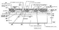
- FIG. 1 adepicts a cross-sectional view of a small active area photodiode wafer 101 a, designed and fabricated using conventional standard technology.
- Wafer 101 ais a photodiode chip 100 a comprising four significant regions, including first region 102 a, second region 103 a, third region 104 a, and fourth region 105 a each having a thickness.
- the specificationscan be changed to suit the design, fabrication and functional requirements suggested herein. From a design standpoint the above-mentioned number of regions and their corresponding thicknesses that comprise the photodiode chip are variable and is merely illustrative of the conventional photodiode structure.
- First region 102 acomprises a suitable substrate material, such as bulk silicon.
- First region 102 amay be heavily doped with a suitable impurity of a selected conductivity type, such as p-type or n-type.
- first region 102 amay possess the following specifications: conductivity of the dopant n-type, thickness 0.400 mm, and resistivity 10-10,000 Ohm cm.
- First region 102 aalso comprises the substrate layer, which further comprises sub-regions 106 a and 107 a.
- Sub-region 106 ais a diffused region, heavily doped with suitable impurities or dopants of a selected conductivity type, such as p-type or n-type.
- diffused region 106 amay be heavily doped with a suitable impurity of the p-type conductivity.
- Sub-region 107 ais typically a depletion region or space charge region (SCR) and serves as the transition region from p-type semiconductor to n-type semiconductor in a p-n junction.
- the depletion regionis an area in which mobile charge carriers have been substantially swept out by an electrical field and hence depleted of carriers. More specifically, the depletion region of a p-n junction in a radiation detector is a region in which the potential energies of two materials, possessing opposite conductivity types, create an energy barrier resulting in an electrical field that depletes the semiconductor of mobile charge carriers.
- the depletion regiontypically has a large electric field, large changes in hole and electron concentrations, large amounts of fixed charge, and a varying potential.
- Second region 103 amay be a junction passivation oxide layer, formed atop the first region 102 a taking into consideration significant parameters.
- Third region 104 ais a shielded region comprising a layer an appropriate material which serves as a protective guard against stray light that irradiates non-active areas and those areas adjacent to active areas. When stray light is absorbed by non-active areas and those areas adjacent to active areas the total photocurrent held by photodiode 100 a is increased.
- Region 104 amay be either one or a combination of a metal shield or a black polyamide layer atop region 103 a.
- Fourth region 105 acomprises a layer of a suitable metal confined to the backside of wafer 101 a.
- a final processing step called backlappingis occasionally performed.
- Backlappingis the process of mechanically thinning the backside of a finished semiconductor wafer.
- the backside of the wafer 101 amay be thinned by employing a wet abrasive solution under pressure.
- backside metallization with a metalsuch as gold (Au) or chromium (Cr) may be deposited on the back of the wafer 101 a via sputtering or evaporation.
- FIG. 1 bis a top view illustration of the small active area photodiode 100 a as shown in FIG. 1 a , depicting photodiode 100 b which comprises active area 101 b, anode 102 b, diffusion boundary area 103 b, gap 104 b, and shielded area 105 b with the appropriate dimensions in accordance with the principles of the standard technology.
- Active area 101 bis designed and fabricated using standard technology. For example, active area photolithography may be employed to design and fabricate active area 101 b.
- the active area specifications, among other parameters,comprise significant performance characteristics of photodiode 100 b.
- Anode area 102 bcomprises a suitable metal material and forms an aperture of appropriate dimension and shape.
- Small active area 101 bis defined by the aperture formed by anode metal 102 b.
- Diffusion boundary area 103 bsurrounds anode metal 102 b and is heavily doped with suitable impurities or dopants of the selected conductivity type, such as p-type or n-type.
- Diffusion boundary area 103 bserves as an area where the photodiode junction is active and can convert photons thus generating current.
- gap area 104 blocated between anode area 102 b and shielded area 105 b, is prone to stray light absorption. Stray light incident on gap 104 b creates undesired stray current, which is electrical current through a path other than the intended path.
- Another disadvantage of the conventional technologyis that if anode area 102 b is extended to the edges of the chip, it results in high MOS capacitance and high dark current.
- the stray lightcontributes to the total photocurrent delivered by the small active area photodiode 100 b and renders the device substantially useless.
- the non-active areas surrounding the active area 101 bmay generate a small photocurrent in the detector as a result of absorption of stray light.
- the magnitude of this photocurrentis dependent upon many parameters, such as the wavelength of the radiation, the applied bias, and the amount of and distance from incident light on active area 101 b.
- Shielded area 105 bblocks stray light incident on the non-active area and in the vicinity of the small active area 101 b .
- Shielded area 105 bmay be fabricated utilizing suitable material for blocking stray light from being absorbed into a non-active area.
- suitable materialfor blocking stray light from being absorbed into a non-active area.
- a metal shield and/or a black polyamide layercan be put on the non-active area as a part of the semiconductor wafer process.
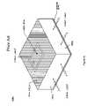
- FIG. 1 cis three-dimensional perspective view of the small active area photodiode as shown in FIGS. 1 a and 1 b .
- FIG. 1 cshows stray, and in particular ambient, light incident on the four facets of photodiode chip 100 c. Upon absorption, the ambient light creates photocarriers that diffuse to depletion region 105 c (not shown) and produce undesired photocurrent that contributes to the total photocurrent, thus creating a disadvantage in the current state of the art.
- the devicemay comprise back surface 107 c, which further comprises a layer of suitable metal.
- the present inventioncomprises a photodiode chip with special structures to substantially reduce detection of stray light thus minimizing the generation of undesired photocurrent.
- the stray light incident on the area between the p+ active area and the rest of the chipis blocked by a plurality of metal layers.
- the small active areais defined by the aperture formed by the second metal shield and exposes the front surface of the photodiode chip.
- a suction diode depletion regionwhich surrounds the active p-n junction effectively collects all carriers generated from stray light incident at the four cutting edges of the photodiode chip.
- the deviceis designed and fabricated as shown in FIGS. 2 a and 2 b.
- the top cathode n+is optional.
- the active area anode padis not connected to other metal, thus eliminating high capacitance or high dark current levels.
- the stray light incident on the area between the p+ active area and the rest of the chipis blocked by a plurality of metal layers. More specifically, a second metal shield blocks stray light incident on the front surface of and in the vicinity of the small active area.
- the p+ active area junctionis surrounded by the p+ suction diode junction.
- the deviceis fabricated on 20 ⁇ m thick epi layer on a heavily doped substrate, thus the suction diode is fully depleted at low bias, and effectively collects all carriers generated from stray light incident at the four cutting edges of the chip.
- FIG. 2 ais a cross-sectional view of wafer 201 , depicting photodiode chip 200 which comprises at least two regions in one embodiment, such as first region 202 and second region 203 .
- the number of regions and their corresponding thicknessis merely illustrative in the above example and is in no way limiting to the present invention.
- First region 202comprises a heavily doped substrate.
- First region 202may be heavily doped with a suitable impurity of a selected conductivity type, such as p-type or n-type.
- first region 202is doped with n-type conductivity and has a thickness of 0.380 mm.
- Second region 203is preferably a single crystal layer, such as but not limited to an epitaxial (epi) layer, formed on the top surface of first region 202 using suitable epitaxy methods.
- Significant parameterssuch as but not limited to material of the epi layer and conductivity type and doping level of the epi layer are taken into consideration.
- second region 203may be doped with n-type conductivity and have a thickness of 0.020 mm.
- the epitaxial layerhas a doping level and/or conductivity type independent of the substrate upon which the epitaxial layer is formed. In some situations the epitaxial layer is of a completely different type of material than the substrate upon which it is grown.
- the epitaxy processhas been described above with reference to the prior art and will not be repeated in this section.
- Second region 203also comprises several diffused sub-regions 204 , 205 , 206 , 207 and 208 , which are diffused into the epi layer.
- diffused sub-regionsare heavily doped with suitable impurities or dopants of the selected conductivity type, such as p-type or n-type.
- diffused sub-regions 204 and 208are heavily doped with a suitable impurity of n-type conductivity
- sub-region 205 , 206 and 207are heavily doped with a suitable impurity of p-type conductivity.
- the n+ layeris in electrical communication with a metal to form a cathode.
- the diffused p+ portionsare in electrical communication with a metal to form an anode.
- diffused sub-regions 204 and 208form part of the optional n+ doped top cathodes.
- Depletion regions(shown in FIG. 2 a with dotted lines) engulf an area formed from the borders and below diffused sub-regions 205 , 206 and 207 .
- diffused sub-regions which form depletion regionsalso form p+ suction diodes.
- the depletion region within the epi layeris that region wherein mobile carriers have been substantially swept out via the formation of an electric field due to the active p-n junction.
- the suction diode depletion regionsurrounds the active p-n junction and collects incident stray light from the four cutting edges of the photodiode chip 200 . If detected, the stray light would generate carriers thus contributing to undesired photocurrent.
- Opening or aperture 209defines a small active area of the photodiode 200 . This formation of this small active area will be discussed in further detail below with reference to FIG. 3 , the flowchart describing the manufacturing process of the photodiode. Aperture 209 is formed from walls created by the second metal layer 225 , also described below.
- Protective layer 210results from subjecting substrate wafer 201 to an initial mask oxidation.
- a semi-insulating polycrystalline silicon (i.e. SIPOS) layer or filmis obtained by adding oxygen or nitrogen to silicon during growth.
- SIPOSis preferred for junction passivation.
- substrate wafer 201is partially covered at selected areas by a protective layer oxidation mask.
- silicon nitrideis used as an oxidation mask. Oxidation masking is well-known to those of ordinary skill in the art and will not be discussed in further detail.
- First metal layer 215is preferably aluminum and fills those portions of substrate wafer 201 not coated with oxide or nitride layer 212 .
- portions of first metal layer 215as shown in FIG. 2 a , overhang and cover layer 210 .
- Polyimide or PECVD low temperature oxide or nitrideis used to form insulation layer 220 . Insulation layer 220 covers those portions of layer 210 that are not coated with the first metal layer 215 .
- Second metal layer 225is an additional layer used to shield against stray light incident on the front surface of and in the vicinity of small active area 209 .
- Small active area 209is defined by an aperture into second metal layer 225 , which is confined to the front surface of photodiode chip 100 .
- a black polyamide layermay be coated on the top surface of the second metal layer to reduce the reflectance of light on the second metal layer.
- FIG. 2 ban expanded cross-sectional view of a preferred embodiment of the small active area photodiode of the present invention with special structures to substantially reduce detection of stray light is depicted.
- FIG. 2 bshows, in a cross-sectional view optional n+ top cathode 204 , small active area 209 , and second metal layer 225 .
- FIG. 3shows flowchart 300 describing one preferred manufacturing process for the small active area photodiode of the present invention with special structures to substantially reduce detection of stray light, as shown in FIGS. 2 a and 2 b .
- the start materialis a round sliced wafer comprised of a suitable semiconductor material.
- a silicon wafermay be used in accordance with the principles of the present invention.
- the wafer or semiconductor device 201has a thickness of 0.380 mm and is heavily doped with a dopant of n-type conductivity.
- the above specificationsare not limiting and may be modified to suit design, fabrication and functional requirements.
- a relatively thin epi layer 203having high resistivity is grown on substrate wafer 201 .
- substrate wafer 201 coated with epi layer 203is subjected to an initial mask oxidation that results in the formation of a protective layer on epi layer 203 .
- a semi-insulating polycrystalline silicon (i.e. SIPOS) layer or filmis obtained by adding oxygen or nitrogen to silicon during growth.
- SIPOSis preferred for junction passivation.
- epi layer 203is partially covered at selected areas by a protective layer oxidation mask.
- the protective layergrows only in those areas upon which layer 203 has been left unmasked.
- silicon nitrideis used as an oxidation mask. Oxidation masking is well-known to those of ordinary skill in the art and will not be discussed in further detail.
- n+ top cathode masking/etchingoccurs and is shown as layers 204 and 208 in FIG. 2 a.
- suitable n+ layersare formed at select regions of the epi layer 203 .
- This processis followed by selective etching.
- the process of masking and selective etchingis well-known to those of ordinary skill in the art and will not be described in further detail herein.
- regions 204 and 208which form part of the n+ top cathodes, are optionally subjected to controlled n+ diffusion.
- controlled n+ diffusionThere are many approaches to this diffusion process possible as are well known to those of ordinary skill in the art and will not be discussed in further detail herein. It is noted however, that the choice of diffusion method is dependent on various factors, including, but not limited to the diffusion coefficient of the dopant, permissible error in diffusion depth, and diffusion source.
- p+ active area and p+ suction diode masking/etchingis performed in step 320 .
- Suitable p+ masksare concurrently applied on the top surface of regions designated as 206 and 207 in FIG. 2 a . Regions 206 and 207 constitute part of the p+ active area and p+ suction diodes not yet formed.
- Epi layer 203 on wafer 201is coated with the protective layer subsequently subjected to selective etching, using the p+ mask to ensure certain regions retain the protective SiO 2 layer.
- Many approaches to this masking and etching techniqueare possible and are well known to those of ordinary skill in the art. They will not be discussed in further detail herein, except in a particular embodiment for reference purposes only and not limiting example.
- a p+ masking processis employed in step 320 .
- the processinvolves first producing a photographic mask of the desired pattern or grid.
- photomasksare high precision plates containing microscopic images of electronic circuits or patterns (also referred to as the geometry of the mask), made from flat pieces of quartz or glass with a layer of chrome on one side. A portion of an electronic circuit or pattern in etched in the chrome.
- p+ masks in the desired geometryare pre-formed for implantation onto a wafer. It should be obvious to one of ordinary skill in the art that other appropriate patterning and masking techniques may be used without departing from the scope of the present invention.
- step 325regions 206 and 207 within the epi layer, masked and etched in step 320 , are subjected to p+ diffusion/oxidation.
- a suitable p+ dopant in a gas, liquid, or solidis employed.
- the choice of diffusion methodis dependent on various factors, including, but not limited to the diffusion coefficient of the dopant, permissible error in diffusion depth, and diffusion source.
- the p+ dopant employed in step 325 of the present inventionis boron. Boron is the only p-type dopant widely used in silicon device manufacturing.
- a protective layeris patterned and etched using a contact window mask to provide contact openings for the n+ top cathodes and anodes for the p+ active area and the p+ suction diode.
- the protective layeris subjected to metallization.
- the selected metalis suitable for the formation of anode and cathode contacts for the photodiode chip 200 in FIG. 2 a of the present invention.
- a first layer of metalis deposited on the entire surface of the protective layer.
- the first layer of metalserves as contacts for the optional n+ top cathodes on sub-regions 204 and 208 as well as for the anodes on the p+ active area and the p+ suction diode on regions 206 and 207 , respectively. While it is preferred that the first metal be comprised of aluminum, one of ordinary skill in the art would appreciate that any suitable metal, which can be processed in accordance with step 335 , may be used.
- step 340after the completion of aluminum metallization in step 335 , the first layer of metal is masked and selectively etched. First, a mask is applied on the first metal layer. Subsequent to application of the mask, the chip is selectively etched, as can be seen in FIG. 2 a.
- the structure of a monolithic integrated circuitcomprises a small plate, or chip, of a semiconductor material wherein the various active and passive circuit components are formed.
- the componentsare interlinked by a connection arrangement provided in a predetermined number of link levels or planes, which are isolated from one another by layers of a dielectric material.
- the first or innermost level in the structureis the diffusion or junction level, and comprises a suitably doped substrate of crystalline silicon. Because it is formed by shaping a layer of metal, such as aluminum, on the integrated circuit surface, the topmost level is referred to as the metallization level. Contacts are formed on this topmost layer for electrically connecting the integrated circuit to its surroundings.
- step 345the aluminum metallization is subjected to “aluminum sintering”.
- “Aluminum sintering”is a process in which fine particles of a material are chemically bonded at a temperature that is sufficient for atomic diffusion. The process of “aluminum sintering” is well-known to those of ordinary skill in the art and will not be discussed in further detail herein. “Aluminum sintering” ensures proper electrical operation at the links between the metallization (topmost) and junction (innermost) levels by both lowering the resistance of the aluminum-silicon contact and reducing the residual valence forces present at the interface of the silicon crystal lattice.
- a polyimide coatingis preferably “spin-coated” on the substrate, but not limited to such application technique.
- the spin-coating techniqueis well known to those of ordinary skill in the art and will not be discussed in further detail.
- Other application techniques that have been usedinclude draw, spray, extrusion, roller, dip and drop coating.
- adhesion promotersare also preferably applied by spin coating.
- step 355 of the present inventionafter spin-coating the substrate with the polyimide layer, a mask is applied.
- the patterning techniques as they relate to masking polyimide layersare well known in the art and will not be discussed in greater detail. It should be noted, however, that polyimide photolithographic processes include, but may not be limited to, the conventional polyimide process which uses a non-photosensitive polyimide and the simplified photosensitive polyimide process which uses a photodefinable or photosensitive polyimide.
- the insulating polyimide layeris then appropriately “etched” to create and opening to the small active area.
- a low temperature oxide or nitridecan be used as an alternative to the polyimide layer. After the PECVD deposition of the low temperature oxide or nitride, standard photolithography techniques and standard etching technology are used to remove the dielectric material from undesired areas.
- step 360the wafer is subjected to a second metallization.
- a second metal layerpreferably but not limited to aluminum, is deposited onto the wafer.
- the metallization processhas already been described above with reference to step 335 and will not be discussed in further detail.
- the metalis subjected to a masking and etching process in step 365 .
- the masking and etching processrequires careful selection and usage of an appropriate metal-containing masking material in combination with a complimentary plasma etchant.
- the byproduct produced by a combination of the metal with the reactive plasma etchant speciesmust be essentially non-volatile under etch process conditions, and sufficiently non-corrosive to features on the substrate being etched, such that the substrate remains unharmed by the etch process.
- aluminumis a preferred metal for the metal-comprising mask
- other metalscan be used for the masking material, as long as they produce an essentially non-volatile, non-corrosive etch byproduct under etch process conditions.
- metallic materials recommended for the maskinclude aluminum, cadmium, copper, chromium, gallium, indium, iron, magnesium, manganese, nickel, and alloys thereof.
- a metal alloysuch as aluminum in combination with copper or magnesium is used, wherein the copper or magnesium content is less than approximately 8% by weight and other constituents total less than about 2% by weight.
- the plasma feed gasincludes at least one fluorine-containing compound such as, but not limited to, nitrogen trifluoride (NF 3 ), carbon tetrafluoride (CF 4 ), and sulfur hexafluoride (SF 6 ). Hydrogen bromide (HBr), Oxygen (O 2 ), or an oxygen-containing compound, or combination thereof may optionally be added to the plasma feed gases to help provide a protective layer thereby assisting in profile control of the etched feature.
- fluorine-containing compoundsuch as, but not limited to, nitrogen trifluoride (NF 3 ), carbon tetrafluoride (CF 4 ), and sulfur hexafluoride (SF 6 ).
- Hydrogen bromide (HBr), Oxygen (O 2 ), or an oxygen-containing compound, or combination thereofmay optionally be added to the plasma feed gases
- metal-containing mask materialetches more slowly than the silicon etch rate, thus ensuring that the etch by-products formed do not harm the etched semiconductor structure or features contained therein. Further, it has been disclosed that if the etch byproducts from the metal-comprising masking material are sufficiently non-volatile, they can be used as “stop” etchants to limit the etch rate of the masking material, thus providing an etch selectivity of silicon relative to the metal-containing masking material in a ratio better than 40:1.
- backside of the substrate waferis metallized, in a process sometimes referred to as “backlapping”.
- Backlappingis the process of mechanically thinning the backside of a finished semiconductor wafer.
- the backside of the wafermay be lapped or ground down using a wet abrasive solution under pressure.
- a chromium-gold (Cr—Au) alloyis deposited on the backside of the wafer via a process called “sputtering”.
Landscapes
- Light Receiving Elements (AREA)
Abstract
Description
- The present invention pertains generally to the field of radiation detectors, and in particular, relates to photodiodes with controlled current leakage.
- Certain photodiodes have two-electrode radiation-sensitive junctions formed in semiconductor material. Light, which illuminates the junction, creates charge carriers. Reverse current varies with illumination. Photodiodes can be photovoltaic or photoconductive devices, used for detection of optical power and subsequent conversion to electrical power.
- Operationally, photodiodes absorb photons or charged particles, facilitating detection of incident optical power and generating current proportional to the incident power, thus converting the incident optical power to electrical power. Light-induced current of the photodiode corresponds to the signal while “dark” current represents noise. “Dark” current is that current that is not induced by light, or that is present in the absence of light. Photodiodes process signals by using the magnitude of the signal-to-noise ratio.
- Photodiodes are typically characterized by certain parameters, such as, among others, electrical characteristics, optical characteristics, current characteristics, voltage characteristics, and noise. Electrical characteristics predominantly comprise shunt resistance, series resistance, junction capacitance, rise or fall time and/or frequency response. Optical characteristics comprise responsivity, quantum efficiency, non-uniformity, and/or non-linearity. Photodiode noise may comprise, among others, thermal noise, quantum, photon or shot noise, and/or flicker noise.
- Conventionally, in an effort to increase the signal to noise ratio and enhance the contrast of the signal, it is desirable to increase the light-induced current of photodiodes. Thus, photodiode sensitivity is enhanced while the overall quality of the photodiode is improved. Photodiode sensitivity is crucial in low-level light applications and is typically quantified by a parameter referred to as noise equivalent power (NEP), which is defined as the optical power that produces a signal-to-noise ratio of one at the detector output. NEP is usually specified at a given wavelength over a frequency bandwidth.
- Essentially active solid-state semiconductor devices, and in particular, silicon photodiodes, are among the most popular photodetectors having a sufficiently high performance over a wide wavelength range with ease of use. Silicon photodiodes are sensitive to light in the wide spectral range, approximately 200*10−9m to 1100*10−9m, extending from deep ultraviolet through visible to near infrared. Silicon photodiodes, by using their ability to detect the presence or absence of minute light intensities, facilitate the extremely precise measurement of these minute light intensities upon appropriate calibration. For example, appropriately calibrated silicon photodiodes detect and measure light intensities varying over a wide range, from very minute light intensities of below 10−13watts/cm2to high intensities above 10−3watts/cm2.
- Conventional photodiodes, as described above, still present numerous problems in their use today. Many of the resources associated with the use of conventional photodiodes, including capital, time, and manpower are wasted in resolving some of the numerous problems including controlling (also referred to as modifying, managing, reducing or eliminating) photodiode leakage current, noise, and stray light. In addition, there are secondary problems that pose problems in conventional photodiode use. These include, but are not limited to, determination and/or selection of apt active area specifications and controlling the higher-wavelength infrared response.
- A particularly serious problem associated with conventional photodiodes is leakage current. Leakage current is a major source of signal offset and noise in applications operating in current mode. More specifically, leakage current flows through the photodiode when it is in a “dark” state, or in the absence of light at a given reverse bias voltage applied across the junction. Leakage current is specified at a particular value of reverse applied voltage. For example, reverse bias voltage may be as low as 10 mV or as high as 50 V, whereas the “dark” currents may vary from pA to μA depending upon the junction area and the process used. Leakage current is temperature dependent; thus, an increase in temperature and reverse bias results in an increase in leakage or dark current. A general rule is that the dark current will approximately double for every 10° C. increase in ambient temperature. It should be noted, however, that specific diode types can vary considerably from this relationship. For example, it is possible that leakage or dark current will approximately double for every 6° C. increase in temperature.
- Various approaches have been used in the prior art to reduce, eliminate or control leakage current. For example, U.S. Pat. No. 4,904,861, assigned to Agilent Technologies, Inc., discloses “an optical encoder comprising: a plurality of active photodiodes in an array on a semiconductor chip; a code member having alternating areas for alternately illuminating and not illuminating the active photodiodes in response to movement of the code member; means connected to the active photodiodes for measuring current from the active photodiodes; and sufficient inactive photodiode area on the semiconductor chip at each end of the array of active photodiodes to make the leakage current to each end active photodiode of the array substantially equal to the leakage current to an active photodiode remote from an end of the array”. Similarly, U.S. Pat. No. 4,998,013, also assigned to Agilent Technologies, Inc. discloses “means for shielding a photodiode from leakage current comprising: at least one active photodiode on a semiconductor chip; means for measuring current from the active photodiode; a shielding area having a photodiode junction substantially surrounding the active photodiode; and means for biasing the shielding area photodiode junction with either zero bias or reverse bias.”
- U.S. Pat. No. 6,670,258, assigned to Digirad Corporation, discloses “a method of fabricating a low-leakage current photodiode array comprising: defining frontside structures for a photodiode on a front side of a substrate; forming a heavily-doped gettering layer on a back surface of the substrate; carrying out a gettering process on the substrate to transport undesired components from the substrate to said gettering layer, and to form another layer in addition to said gettering layer, which is a heavily-doped, conductive, crystalline layer within the substrate; after said gettering process, removing the entire gettering layer; and after said removing, thinning the heavily-doped, conductive, crystalline layer within the substrate to create a native optically transparent, conductive bias electrode layer”.
- Similarly, U.S. Pat. No. 6,734,416, also assigned to Digirad Corporation, discloses “a low-leakage current photodiode array comprising: a substrate having a front side and a back side; a plurality of gate regions formed near the front side of the substrate; a backside layer formed within the substrate, near the back side of the substrate, the backside layer having a thickness of approximately 0.25 to 1.0 micrometers and having a sheet resistivity of approximately 50 to 1000 Ohm per square.”
- U.S. Pat. No. 6,569,700, assigned to United Microelectronics Corporation in Taiwan, discloses “1. A method of reducing leakage current of a photodiode on a semiconductor wafer, the surface of the semiconductor wafer comprising a p-type substrate, a photosensing area for forming a photosensor of the photodiode, and a shallow trench positioned in the substrate surrounding the photosensing area, the method comprising: forming a doped polysilicon layer containing p-type dopants in the shallow trench; using a thermal process to cause the p-type dopants in the doped polysilicon layer to diffuse into portions of the p-type substrate that surround a bottom of the shallow trench and walls of the shallow trench; removing the doped polysilicon layer; filling an insulator into the shallow trench to form a shallow trench isolation (STI) structure; performing a first ion implantation process to form a first n-type doped region in the photosensing area; and performing a second ion implantation process to form a second n-type doped region in the photosensing area.”
- Also, U.S. Pat. No. 6,504,158, assigned to General Electric Company, discloses “a method of reducing leakage current in an imaging apparatus, including: providing a substrate with at least one radiation-sensitive imaging region therein; forming a guard region in the substrate at or immediately adjacent a cut edge of the substrate to reduce leakage current reaching the at least one radiation-sensitive imaging region from the cut edge when the imaging apparatus is in use; and electrically reverse biasing the at least one radiation-sensitive imaging region and the guard region relative to the substrate.”
- In addition to leakage current, noise is often a limiting factor for the performance of any device or system. In almost every area of measurement, the limit to the detectability of signals is set by noise, or unwanted signals that obscure the desired signal. As described above, the NEP is used to quantify detector noise. Noise issues generally have an important effect on device or system cost. For example, the reduction of quantum or shot noise influence in interferometers for gravitational wave detection greatly lessens required interferometer arm length. Conventional photodiodes are particularly sensitive to noise issues. Like other types of light sensors, the lower limits of light detection for photodiodes are determined by the noise characteristics of the device.
- As described above, the typical noise components in photodiodes include thermal noise; quantum or shot noise; and flicker noise in that order. These noise components collectively contribute to the total noise in the photodiode. Thermal noise, or Johnson noise, is inversely related to the value of the shunt resistance of photodiode and tends to be the dominant noise component when the diode is operated under zero applied reverse bias conditions. Shot noise is dependent upon the leakage or dark current of photodiode and is generated by random fluctuations of current flowing through the device, which may be either dark current or photocurrent. Shot noise tends to dominate when the photodiode is used in photoconductive mode where an external reverse bias is applied across the device. As an example, detector noise generated by a planar diffused photodiode operating in the reverse bias mode is a combination of both shot noise and thermal noise. Flicker noise, unlike thermal or shot noise, bears an inverse relationship to spectral density. Flicker noise may dominate when the bandwidth of interest contains frequencies less than 1 kHz.
- In addition to leakage current and noise issues, photodiodes are susceptible to absorption of unwanted or stray light. Stray light is typically that light which propagates through a path other than that which is intended (thus reaching the detector) and excludes the wavelength of interest or an erroneous wavelength. Stray light activates a signal at the detector element. Some of the recognized sources of stray light include ambient light, scattering light from imperfect optical components and/or reflections of non-optical components. The ambient or stray light is assumed to be stationary or slowly fluctuating. Stationary ambient light engenders shot noise, owing to the statistical nature of the production of photocarriers upon impinging on the photodetector. In certain circumstances, the photodiode is exposed to ambient or stray light thus resulting in a high level of noise. Additionally, stray light influences the signal-to-noise ratio (S/N or SNR) and introduces non-linearity.
- While photodiodes have a wide viewing angle, many applications require the detection of desired light and concurrent rejection of stray light. Stray light absorption significantly contributes to the total photocurrent delivered by a small active area photodiode and renders it not usable. For example, photodiodes typically used in medical applications need to deliver a precise ratio of photocurrents illuminated from 660 nm and 880 nm. It is possible that an incorrect ratio of photocurrents will be delivered due to the absorption or collection of stray light by the photodiode.
- Some attempts have been made in the prior art to correct for the effects of stray light. For example, U.S. Pat. No. 5,869,834, assigned to Sitek Electro Optics, discloses “a position-sensitive photodetector for measuring the position of an incident light beam having energy, comprising: a semiconductor wafer having a doped active surface and a pair of ends; a resistive layer on the active surface of the wafer; two opposed electrodes on each end of said active surface; a stray-light area arranged externally around the active surface, said stray-light area for measuring stray-light contacting said photodetector and for preventing said stray light from affecting a position measuring signal of said incident light beam, said stray light area comprising a doped area containing a p-n junction and a grounding electrode attached thereto, the signal from said stray light area being grounded; a first inactive area externally surrounding said stray-light area and a second inactive area disposed between said active area and said stray-light area, each inactive area connected to said same ground as said stray-light area.”
- Also, U.S. Pat. No. 6,546,171, assigned to NEC Corporation, discloses “a structure for shielding a stray light in an optical waveguide module, comprising: an optical waveguide substrate supported in an optical waveguide module package; a laser diode (LD) which is mounted on said optical waveguide substrate and emits a first signal light; an optical waveguide which is formed on said optical waveguide substrate and propagates a part of said first signal light; a wavelength divisional multiplexing (WDM, hereinafter) filter which is formed on said optical waveguide substrate; an optical fiber which is situated on said optical waveguide substrate and transmits said part of said first signal light to an optical transmission line; a photodiode (PD, hereinafter) for receiving a second signal light which is propagated through said optical transmission line and transmitted through said WDM filter via said optical waveguide; and a metallic layer which is evaporated on a surface of said WDM filter and provided with a pin hole for transmitting said second signal light to said PD via said WDM filter, wherein a remaining part of said first signal light (a stray light, hereinafter) which is not optically coupled with said optical waveguide is reflected by said metallic layer so that said stray light is prevented from being coupled with said PD.”
- As discussed earlier, secondary issues also contribute to dark noise and other noise sources that impact photodiode sensitivity. These include primarily determination and/or selection of apt active area specifications (geometry and dimensions), response speed, quantum efficiency at the wavelength of interest, response linearity, and spatial uniformity of response, among others.
- While methods and systems of the prior art described above may improve performance, they do not effectively control leakage current, which is equally important to high-performance as well as low-standby and low-power operation devices. Thus, there is still a need for photodiodes with controlled leakage current. Additionally, there is need for low-voltage, low-power designs vis-à-vis photodiodes with aggressive techniques for controlling leakage current. In addition, in spite of the attempts in the prior art, as described above, to reduce or eliminate the effects of stray light absorption with respect to photodiodes, no attempt has been made to design and fabricate photodiodes with special structures to completely avoid stray light.
- Thus, there is a need for the design and implementation of methods and apparatuses which completely avoid stray light absorption, reduce or eliminate noise, and control leakage current while lessening the effects of these noise contributing factors. More specifically, what is needed is a photodiode design and fabrication method intended for applications wherein a small active area is employed and wherein a complete avoidance of stray light is of greater importance.
- It is an object of the present invention to design and manufacture photodiodes with controlled leakage current. More specifically, the present invention provides low-voltage, low-power photodiodes with aggressive and effective techniques for controlling leakage current. It is also an object of the present invention to provide a method of reducing leakage current of a photodiode that increases signal-to-noise ratio and sensitivity. Thus, the present invention also reduces or nullifies noise in photodiodes.
- Yet another object of the present invention is to design and fabricate photodiodes with special structures to completely avoid detection of stray light. Also, it an objective of the present invention to reduce or minimize, and even more preferably, avoid, stray light absorption.
- In one embodiment, the present invention is a photodiode array comprising a substrate having at least a front side and a back side; a plurality of photodiodes integrally formed in the substrate forming said array; a plurality of electrical contacts in electrical communication with said front side; a plurality of suction diodes positioned at selected locations within the array; and at least one metal layer on said array, wherein the fabrication of said array involves a masking process comprising the steps of applying a first metallization layer on said front side and applying a second metallization layer on said front side and subsequently creating an aperture to an active area.
- In another embodiment, the present invention is a photodiode array comprising a substrate having at least a front side and a back side; a plurality of photodiodes integrally formed in the substrate forming the said array; a plurality of electrical contacts in electrical communication with said front side; and a plurality of suction diodes positioned at selected locations within the array, wherein the fabrication of said array involves a masking process comprising the steps of applying a n+ mask on said front side, applying a p+ mask on said front side, applying a first metal layer of said front side, applying an insulation layer on said front side, and applying a second metal layer on said front side.
- Optionally, the second metallization layer on the front side substantially prevents stray light from impinging upon the areas surrounding the active area. The substrate is made of n-doped silicon. Each of the plurality of photodiodes and suction diodes have a front surface and the front surface is partially covered by passivated oxidized junction, an insulating layer, and a first metal layer. The insulating layer is a polymide. The insulating layer is a low temperature oxide or nitride layer. The front side optionally comprises a n+ layer in electrical communication with a metal to form a cathode. The front layer comprises a doped material of p+ conductivity type. The front p+ layer is in electrical communication with a metal to form an anode.
- In one embodiment, the present invention includes a photodiode array comprising a substrate having at least a front side and a back side; a plurality of photodiodes integrally formed in the substrate forming the array; a plurality of electrical contacts in electrical communication with the front side; and a plurality of suction diodes positioned at selected locations within the array. The fabrication of the array involves a masking process comprising the steps of applying a n+ mask on said front side, applying a p+ mask on the front side, applying a first metal layer of the front side, applying an insulation layer on the front side, and applying a second metal layer on the front side.
- Optionally, the masking process further comprises etching the second metal layer to form an aperture leading to an active area on the photodiode. The second metal layer prevents stray light from impinging on the areas surrounding the active area. The front layer comprises a doped material of n+ conductivity type. The front n+ layer is in electrical communication with a metal to form a cathode. The front layer comprises a doped material of p+ conductivity type. The front p+ layer is in electrical communication with a metal to form a cathode. The insulation layer is a polymide.
- Although several embodiments that remedy the aforementioned shortcomings in connection to the photodiodes will be readily apparent to those of ordinary skill in the art, the disclosure set forth herein may be applicable to other embodiments and applications without departing from the spirit and scope of the present invention and the claims hereto appended.
- These and other features and advantages of the present invention will be appreciated, as they become better understood by reference to the following Detailed Description when considered in connection with the accompanying drawings, wherein:
FIG. 1 ais a cross-sectional view of a conventional small active area photodiode, designed and fabricated using standard technology;FIG. 1 bis a top view of the small active area photodiode ofFIG. 1 a;FIG. 1 cis a three-dimensional perspective view of the small active area photodiode as shown inFIGS. 1 aand1b;FIG. 2 adepicts a cross-sectional view of one embodiment of the small active area photodiode of the present invention with special structures to substantially reduce, and preferably avoid, detection of stray light;FIG. 2 bdepicts a top view of one embodiment of the small active area photodiode of the present invention with special structures to substantially reduce detection of stray light; andFIG. 3 is a flowchart describing one manufacturing process for the small active area photodiode of the present invention with special structures to substantially reduce detection of stray light, as shown inFIGS. 2 aand2b.- The present invention is directed towards radiation detectors and methods of detecting incident radiation. In particular the present invention is directed towards photodiodes with controlled current leakage detector structures and a method of manufacturing photodiodes with controlled current leakage detector structures. More specifically, the present invention discloses photodiodes with special structures to substantially reduce detection of stray light. Additionally, the present invention gives special emphasis to design, fabrication, and use of photodiodes with controlled leakage current.
- Various modifications to the preferred embodiment, disclosed herein, will be readily apparent to those of ordinary skill in the art and the disclosure set forth herein may be applicable to other embodiments and applications without departing from the spirit and scope of the present invention and the claims hereto appended. Thus, the present invention is not intended to be limited to the embodiments described, but is to be accorded the broadest scope consistent with the disclosure set forth herein.
- Conventionally, the active area in detectors is either of a round or square shape. There is no restriction on the shape of these active areas, however. Many applications may require triangular, radial, or trapezoidal shapes. Conventional photodiodes are manufactured via standard wafer fabrication techniques involving methods of masking and photoetching; thus, it is relatively simple to create a unique geometry. The geometric size and shape of the active area can be held to tolerances of 2 microns. As described herein, the term “region” is used interchangeably with the term “area” and refers to discrete portions within the photodiode chip.
- In a conventional prior art embodiment, a small active area silicon photodiode is designed and fabricated using standard technology. The specifications of the designated active area include shape and dimension specifics. Other parameters that are carefully designed are those which comprise significant performance characteristics of photodiodes, including but not limited to, response speed, quantum efficiency at the wavelength of interest, response linearity, spatial uniformity of response, dark noise or other noise sources that impact photodiode noise equivalent power.
- As shown in
FIGS. 1 a,1b, and1c, an exemplary prior art photodiode comprises a 30 μm×30 μm small active area designed and fabricated using standard technology. The 30 μm×30 μm opening cut into the anode metal defines the active area. In order to prevent incident stray light from impinging on the outside areas, a metal shield is placed on the four outside borders of the p+ diffusedarea 104a.There is, however, a non-metallized gap between the anode metal and the metal shield. The stray light incident on this gap will result in undesired stray current. Note that if the anode metal is extended to the edges of the chip, the device has high MOS capacitance and high dark current. Another disadvantage of the standard technology of the prior art is that ambient room stray light is incident on the four edges of the chip. The resultant absorbed stray light will generate carriers, which will diffuse to the depletion region of the p+ diffuse active junction, thus producing undesired photocurrent. - Referring now to
FIGS. 1 a,1b, and1c,a conventional photodiode is described in greater detail to help elucidate its differences with the present invention.FIG. 1 adepicts a cross-sectional view of a small activearea photodiode wafer 101a,designed and fabricated using conventional standard technology.Wafer 101ais aphotodiode chip 100acomprising four significant regions, includingfirst region 102a,second region 103a,third region 104a,andfourth region 105aeach having a thickness. The specifications, however, can be changed to suit the design, fabrication and functional requirements suggested herein. From a design standpoint the above-mentioned number of regions and their corresponding thicknesses that comprise the photodiode chip are variable and is merely illustrative of the conventional photodiode structure. First region 102acomprises a suitable substrate material, such as bulk silicon.First region 102amay be heavily doped with a suitable impurity of a selected conductivity type, such as p-type or n-type. For example,first region 102amay possess the following specifications: conductivity of the dopant n-type, thickness 0.400 mm, and resistivity 10-10,000 Ohm cm.First region 102aalso comprises the substrate layer, which further comprisessub-regions Sub-region 106ais a diffused region, heavily doped with suitable impurities or dopants of a selected conductivity type, such as p-type or n-type. For example, diffusedregion 106amay be heavily doped with a suitable impurity of the p-type conductivity.Sub-region 107ais typically a depletion region or space charge region (SCR) and serves as the transition region from p-type semiconductor to n-type semiconductor in a p-n junction. The depletion region is an area in which mobile charge carriers have been substantially swept out by an electrical field and hence depleted of carriers. More specifically, the depletion region of a p-n junction in a radiation detector is a region in which the potential energies of two materials, possessing opposite conductivity types, create an energy barrier resulting in an electrical field that depletes the semiconductor of mobile charge carriers. The depletion region typically has a large electric field, large changes in hole and electron concentrations, large amounts of fixed charge, and a varying potential.Second region 103amay be a junction passivation oxide layer, formed atop thefirst region 102ataking into consideration significant parameters.Third region 104ais a shielded region comprising a layer an appropriate material which serves as a protective guard against stray light that irradiates non-active areas and those areas adjacent to active areas. When stray light is absorbed by non-active areas and those areas adjacent to active areas the total photocurrent held byphotodiode 100ais increased.Region 104amay be either one or a combination of a metal shield or a black polyamide layer atopregion 103a.Fourth region 105acomprises a layer of a suitable metal confined to the backside ofwafer 101a.In the standard technology, a final processing step called backlapping is occasionally performed. Backlapping is the process of mechanically thinning the backside of a finished semiconductor wafer. The backside of thewafer 101amay be thinned by employing a wet abrasive solution under pressure. Subsequently, backside metallization with a metal such as gold (Au) or chromium (Cr) may be deposited on the back of thewafer 101avia sputtering or evaporation.FIG. 1 bis a top view illustration of the smallactive area photodiode 100aas shown inFIG. 1 a, depictingphotodiode 100bwhich comprisesactive area 101b,anode 102b,diffusion boundary area 103b,gap 104b,and shieldedarea 105bwith the appropriate dimensions in accordance with the principles of the standard technology.Active area 101b,referred to hereinafter as “small active area” or “active area”, is designed and fabricated using standard technology. For example, active area photolithography may be employed to design and fabricateactive area 101b.The active area specifications, among other parameters, comprise significant performance characteristics ofphotodiode 100b.Anode area 102b,comprises a suitable metal material and forms an aperture of appropriate dimension and shape. Smallactive area 101bis defined by the aperture formed byanode metal 102b.Diffusion boundary area 103b,surroundsanode metal 102band is heavily doped with suitable impurities or dopants of the selected conductivity type, such as p-type or n-type.Diffusion boundary area 103bserves as an area where the photodiode junction is active and can convert photons thus generating current.- One particular disadvantage of fabricating and designing small active area photodiodes in the conventional technology is that
gap area 104blocated betweenanode area 102band shieldedarea 105b,is prone to stray light absorption. Stray light incident ongap 104bcreates undesired stray current, which is electrical current through a path other than the intended path. Another disadvantage of the conventional technology is that ifanode area 102bis extended to the edges of the chip, it results in high MOS capacitance and high dark current. - The stray light contributes to the total photocurrent delivered by the small
active area photodiode 100band renders the device substantially useless. Thus, the non-active areas surrounding theactive area 101bmay generate a small photocurrent in the detector as a result of absorption of stray light. The magnitude of this photocurrent is dependent upon many parameters, such as the wavelength of the radiation, the applied bias, and the amount of and distance from incident light onactive area 101b. - Shielded
area 105bblocks stray light incident on the non-active area and in the vicinity of the smallactive area 101b. Shieldedarea 105bmay be fabricated utilizing suitable material for blocking stray light from being absorbed into a non-active area. For example, a metal shield and/or a black polyamide layer can be put on the non-active area as a part of the semiconductor wafer process. FIG. 1 cis three-dimensional perspective view of the small active area photodiode as shown inFIGS. 1 aand1b.FIG. 1 cshows stray, and in particular ambient, light incident on the four facets ofphotodiode chip 100c.Upon absorption, the ambient light creates photocarriers that diffuse to depletion region105c(not shown) and produce undesired photocurrent that contributes to the total photocurrent, thus creating a disadvantage in the current state of the art. Further, the device may comprise back surface107c,which further comprises a layer of suitable metal.- Now referring to
FIGS. 2 a,2b,and3 an embodiment of the present invention is described. In a preferred embodiment, the present invention comprises a photodiode chip with special structures to substantially reduce detection of stray light thus minimizing the generation of undesired photocurrent. The carriers generated due to the detection of stray light incident on a photodiode, either from ambient light or outside, contribute to the generation of undesired photocurrent. The stray light incident on the area between the p+ active area and the rest of the chip is blocked by a plurality of metal layers. The small active area is defined by the aperture formed by the second metal shield and exposes the front surface of the photodiode chip. In addition, a suction diode depletion region which surrounds the active p-n junction effectively collects all carriers generated from stray light incident at the four cutting edges of the photodiode chip. - In order to substantially reduce the detection of stray light, the device is designed and fabricated as shown in
FIGS. 2 aand2b.In such device, the top cathode n+ is optional. In addition, the active area anode pad is not connected to other metal, thus eliminating high capacitance or high dark current levels. The stray light incident on the area between the p+ active area and the rest of the chip is blocked by a plurality of metal layers. More specifically, a second metal shield blocks stray light incident on the front surface of and in the vicinity of the small active area. The p+ active area junction is surrounded by the p+ suction diode junction. As mentioned above, any stray light incident at the four edges of the chip will be collected in the depletion region of the suction diodes. In one embodiment, the device is fabricated on 20 μm thick epi layer on a heavily doped substrate, thus the suction diode is fully depleted at low bias, and effectively collects all carriers generated from stray light incident at the four cutting edges of the chip. FIG. 2 ais a cross-sectional view ofwafer 201, depicting photodiode chip200 which comprises at least two regions in one embodiment, such asfirst region 202 andsecond region 203. The number of regions and their corresponding thickness is merely illustrative in the above example and is in no way limiting to the present invention.First region 202 comprises a heavily doped substrate.First region 202 may be heavily doped with a suitable impurity of a selected conductivity type, such as p-type or n-type. For example, but not limited to such example,first region 202 is doped with n-type conductivity and has a thickness of 0.380 mm.Second region 203 is preferably a single crystal layer, such as but not limited to an epitaxial (epi) layer, formed on the top surface offirst region 202 using suitable epitaxy methods. Significant parameters, such as but not limited to material of the epi layer and conductivity type and doping level of the epi layer are taken into consideration. For example, but not limited to such example,second region 203 may be doped with n-type conductivity and have a thickness of 0.020 mm.- As described above, typically, the epitaxial layer has a doping level and/or conductivity type independent of the substrate upon which the epitaxial layer is formed. In some situations the epitaxial layer is of a completely different type of material than the substrate upon which it is grown. The epitaxy process has been described above with reference to the prior art and will not be repeated in this section.
Second region 203 also comprises several diffusedsub-regions sub-regions sub-region sub-regions FIG. 2 awith dotted lines) engulf an area formed from the borders and below diffusedsub-regions - Opening or
aperture 209 defines a small active area of the photodiode200. This formation of this small active area will be discussed in further detail below with reference toFIG. 3 , the flowchart describing the manufacturing process of the photodiode.Aperture 209 is formed from walls created by thesecond metal layer 225, also described below. Protective layer 210 results from subjectingsubstrate wafer 201 to an initial mask oxidation. For example, and not limited to such example, a semi-insulating polycrystalline silicon (i.e. SIPOS) layer or film is obtained by adding oxygen or nitrogen to silicon during growth. The use of SIPOS is preferred for junction passivation. To formprotective layer 210,substrate wafer 201 is partially covered at selected areas by a protective layer oxidation mask. Preferably, but not limited to such example, silicon nitride is used as an oxidation mask. Oxidation masking is well-known to those of ordinary skill in the art and will not be discussed in further detail.- After the diffusion step to form the p-n junction, an anti-reflective oxide or
nitride layer 212 is thermally grown or deposited on the active area.First metal layer 215 is preferably aluminum and fills those portions ofsubstrate wafer 201 not coated with oxide ornitride layer 212. In addition, portions offirst metal layer 215, as shown inFIG. 2 a, overhang andcover layer 210. Polyimide or PECVD low temperature oxide or nitride is used to forminsulation layer 220.Insulation layer 220 covers those portions oflayer 210 that are not coated with thefirst metal layer 215. Second metal layer 225 is an additional layer used to shield against stray light incident on the front surface of and in the vicinity of smallactive area 209. Smallactive area 209 is defined by an aperture intosecond metal layer 225, which is confined to the front surface of photodiode chip100. Optionally, a black polyamide layer may be coated on the top surface of the second metal layer to reduce the reflectance of light on the second metal layer.- Various modifications to the design and specifications disclosed above will be readily apparent to those of ordinary skill in the art. Thus, the particular embodiment and design approach disclosed above is in no way intended to be limiting and other possible modifications to the current design approach may be easily adopted while still adhering to the spirit and scope of the present invention and the claims appended hereto.
- Referring now to
FIG. 2 b,an expanded cross-sectional view of a preferred embodiment of the small active area photodiode of the present invention with special structures to substantially reduce detection of stray light is depicted.FIG. 2 bshows, in a cross-sectional view optional n+top cathode 204, smallactive area 209, andsecond metal layer 225. FIG. 3 shows flowchart300 describing one preferred manufacturing process for the small active area photodiode of the present invention with special structures to substantially reduce detection of stray light, as shown inFIGS. 2 aand2b. Reference will be made to the layers represented inFIGS. 2 aand2bwhere appropriate.- In an exemplary embodiment, but not limited to such example, the start material is a round sliced wafer comprised of a suitable semiconductor material. For example, a silicon wafer may be used in accordance with the principles of the present invention. In one preferred embodiment, the wafer or
semiconductor device 201 has a thickness of 0.380 mm and is heavily doped with a dopant of n-type conductivity. The above specifications are not limiting and may be modified to suit design, fabrication and functional requirements. A relativelythin epi layer 203, having high resistivity is grown onsubstrate wafer 201. - As shown in
step 305,substrate wafer 201 coated withepi layer 203, is subjected to an initial mask oxidation that results in the formation of a protective layer onepi layer 203. For example, and not limited to such example, a semi-insulating polycrystalline silicon (i.e. SIPOS) layer or film is obtained by adding oxygen or nitrogen to silicon during growth. The use of SIPOS is preferred for junction passivation. Instep 305,epi layer 203 is partially covered at selected areas by a protective layer oxidation mask. As a result, the protective layer grows only in those areas upon whichlayer 203 has been left unmasked. Preferably, but not limited to such example, silicon nitride is used as an oxidation mask. Oxidation masking is well-known to those of ordinary skill in the art and will not be discussed in further detail. - In
step 310, n+ top cathode masking/etching occurs and is shown aslayers FIG. 2 a.Thus, suitable n+ layers are formed at select regions of theepi layer 203. This process is followed by selective etching. The process of masking and selective etching is well-known to those of ordinary skill in the art and will not be described in further detail herein. - In step315,
regions - Once the optional n+ top cathode diffusion is complete, p+ active area and p+ suction diode masking/etching is performed in
step 320. Suitable p+ masks are concurrently applied on the top surface of regions designated as206 and207 inFIG. 2 a.Regions Epi layer 203 onwafer 201 is coated with the protective layer subsequently subjected to selective etching, using the p+ mask to ensure certain regions retain the protective SiO2layer. Many approaches to this masking and etching technique are possible and are well known to those of ordinary skill in the art. They will not be discussed in further detail herein, except in a particular embodiment for reference purposes only and not limiting example. - Preferably, a p+ masking process is employed in
step 320. The process involves first producing a photographic mask of the desired pattern or grid. Preferably, photomasks are high precision plates containing microscopic images of electronic circuits or patterns (also referred to as the geometry of the mask), made from flat pieces of quartz or glass with a layer of chrome on one side. A portion of an electronic circuit or pattern in etched in the chrome. Typically, p+ masks in the desired geometry are pre-formed for implantation onto a wafer. It should be obvious to one of ordinary skill in the art that other appropriate patterning and masking techniques may be used without departing from the scope of the present invention. - In step325,
regions step 320, are subjected to p+ diffusion/oxidation. Preferably, a suitable p+ dopant in a gas, liquid, or solid is employed. There are many approaches to this diffusion process possible as are well known to those of ordinary skill in the art and will not be discussed in further detail herein. It is noted however, that the choice of diffusion method is dependent on various factors, including, but not limited to the diffusion coefficient of the dopant, permissible error in diffusion depth, and diffusion source. For example, but not limited to such example, the p+ dopant employed in step325 of the present invention is boron. Boron is the only p-type dopant widely used in silicon device manufacturing. - In
step 330, a protective layer is patterned and etched using a contact window mask to provide contact openings for the n+ top cathodes and anodes for the p+ active area and the p+ suction diode. - Following removal of the contact window mask, in
step 335, the protective layer is subjected to metallization. The selected metal is suitable for the formation of anode and cathode contacts for the photodiode chip200 inFIG. 2 aof the present invention. A first layer of metal is deposited on the entire surface of the protective layer. Upon further processing, as will be discussed in greater detail below, the first layer of metal serves as contacts for the optional n+ top cathodes onsub-regions regions step 335, may be used. - In
step 340, after the completion of aluminum metallization instep 335, the first layer of metal is masked and selectively etched. First, a mask is applied on the first metal layer. Subsequent to application of the mask, the chip is selectively etched, as can be seen inFIG. 2 a. - In general, the structure of a monolithic integrated circuit comprises a small plate, or chip, of a semiconductor material wherein the various active and passive circuit components are formed. The components are interlinked by a connection arrangement provided in a predetermined number of link levels or planes, which are isolated from one another by layers of a dielectric material. Typically, the first or innermost level in the structure is the diffusion or junction level, and comprises a suitably doped substrate of crystalline silicon. Because it is formed by shaping a layer of metal, such as aluminum, on the integrated circuit surface, the topmost level is referred to as the metallization level. Contacts are formed on this topmost layer for electrically connecting the integrated circuit to its surroundings.
- Proper functionality of an integrated circuit is associated with the method of linking junction (innermost) level to the metallization (topmost) level. As is known to those of ordinary skill in the art, linking must occur at a predetermined fixed signal voltage or “threshold”, and becomes more critical to achieve as its size decreases. In order to achieve this requirement, it is current practice to treat via “aluminum annealing” or “aluminum sintering”.
- In
step 345, the aluminum metallization is subjected to “aluminum sintering”. “Aluminum sintering” is a process in which fine particles of a material are chemically bonded at a temperature that is sufficient for atomic diffusion. The process of “aluminum sintering” is well-known to those of ordinary skill in the art and will not be discussed in further detail herein. “Aluminum sintering” ensures proper electrical operation at the links between the metallization (topmost) and junction (innermost) levels by both lowering the resistance of the aluminum-silicon contact and reducing the residual valence forces present at the interface of the silicon crystal lattice. - In
step 350 of the present invention, a polyimide coating is preferably “spin-coated” on the substrate, but not limited to such application technique. The spin-coating technique is well known to those of ordinary skill in the art and will not be discussed in further detail. Other application techniques that have been used include draw, spray, extrusion, roller, dip and drop coating. For optimal adhesion to silicon, oxides, and most metal, it is preferred that the polyimide coating be used in conjunction with adhesion promoters. Some polyimides contain adhesion promoters, while others require the application of a separate adhesion promoter or coupler prior to polyimide application. When used separately, adhesion promoters are also preferably applied by spin coating. - In
step 355 of the present invention, after spin-coating the substrate with the polyimide layer, a mask is applied. The patterning techniques as they relate to masking polyimide layers are well known in the art and will not be discussed in greater detail. It should be noted, however, that polyimide photolithographic processes include, but may not be limited to, the conventional polyimide process which uses a non-photosensitive polyimide and the simplified photosensitive polyimide process which uses a photodefinable or photosensitive polyimide. The insulating polyimide layer is then appropriately “etched” to create and opening to the small active area. Optionally, as an alternative to the polyimide layer, a low temperature oxide or nitride can be used. After the PECVD deposition of the low temperature oxide or nitride, standard photolithography techniques and standard etching technology are used to remove the dielectric material from undesired areas. - In
step 360, the wafer is subjected to a second metallization. A second metal layer, preferably but not limited to aluminum, is deposited onto the wafer. The metallization process has already been described above with reference to step335 and will not be discussed in further detail. - Subsequent to the aluminum metallization step, the metal is subjected to a masking and etching process in
step 365. The masking and etching process requires careful selection and usage of an appropriate metal-containing masking material in combination with a complimentary plasma etchant. The byproduct produced by a combination of the metal with the reactive plasma etchant species must be essentially non-volatile under etch process conditions, and sufficiently non-corrosive to features on the substrate being etched, such that the substrate remains unharmed by the etch process. Although aluminum is a preferred metal for the metal-comprising mask, other metals can be used for the masking material, as long as they produce an essentially non-volatile, non-corrosive etch byproduct under etch process conditions. For example, and not limited to such example, metallic materials recommended for the mask include aluminum, cadmium, copper, chromium, gallium, indium, iron, magnesium, manganese, nickel, and alloys thereof. - In one embodiment, a metal alloy such as aluminum in combination with copper or magnesium is used, wherein the copper or magnesium content is less than approximately 8% by weight and other constituents total less than about 2% by weight. The plasma feed gas includes at least one fluorine-containing compound such as, but not limited to, nitrogen trifluoride (NF3), carbon tetrafluoride (CF4), and sulfur hexafluoride (SF6). Hydrogen bromide (HBr), Oxygen (O2), or an oxygen-containing compound, or combination thereof may optionally be added to the plasma feed gases to help provide a protective layer thereby assisting in profile control of the etched feature.
- Typically, metal-containing mask material etches more slowly than the silicon etch rate, thus ensuring that the etch by-products formed do not harm the etched semiconductor structure or features contained therein. Further, it has been disclosed that if the etch byproducts from the metal-comprising masking material are sufficiently non-volatile, they can be used as “stop” etchants to limit the etch rate of the masking material, thus providing an etch selectivity of silicon relative to the metal-containing masking material in a ratio better than 40:1.
- Finally, in step370, the backside of the substrate wafer is metallized, in a process sometimes referred to as “backlapping”. Backlapping is the process of mechanically thinning the backside of a finished semiconductor wafer. The backside of the wafer may be lapped or ground down using a wet abrasive solution under pressure. In a preferred embodiment, a chromium-gold (Cr—Au) alloy is deposited on the backside of the wafer via a process called “sputtering”.
- Various modifications to the manufacturing process, disclosed above, will be readily apparent to those of ordinary skill in the art. Thus, this process is in no way intended to be limiting and those other possible modifications to the current manufacturing process may be easily adopted while still abiding by the spirit and scope of the present invention and the claims appended hereto. It should be understood that the present invention may be modified to incorporate other possible embodiments.
- The above examples are merely illustrative of the many applications of the system of present invention. Although only a few embodiments of the present invention have been described herein, it should be understood that the present invention might be embodied in many other specific forms without departing from the spirit or scope of the invention. Therefore, the present examples and embodiments are to be considered as illustrative and not restrictive, and the invention is not to be limited to the details given herein, but may be modified within the scope of the appended claims.
Claims (17)
Priority Applications (6)
| Application Number | Priority Date | Filing Date | Title |
|---|---|---|---|
| US12/325,304US7898055B2 (en) | 2005-03-16 | 2008-12-01 | Photodiode with controlled current leakage |
| US12/709,621US8519503B2 (en) | 2006-06-05 | 2010-02-22 | High speed backside illuminated, front side contact photodiode array |
| US12/722,685US8035183B2 (en) | 2003-05-05 | 2010-03-12 | Photodiodes with PN junction on both front and back sides |
| US13/225,245US20120061788A1 (en) | 2003-05-05 | 2011-09-02 | Photodiodes with pn-junction on both front and back sides |
| US13/955,299US8907440B2 (en) | 2003-05-05 | 2013-07-31 | High speed backside illuminated, front side contact photodiode array |
| US14/531,287US20150137302A1 (en) | 2006-06-05 | 2014-11-03 | High Speed Backside Illuminated, Front Side Contact Photodiode Array |
Applications Claiming Priority (3)
| Application Number | Priority Date | Filing Date | Title |
|---|---|---|---|
| US11/081,219US7256470B2 (en) | 2005-03-16 | 2005-03-16 | Photodiode with controlled current leakage |
| US11/774,022US7590961B2 (en) | 2004-08-24 | 2007-07-06 | Integrated circuit with signal skew adjusting cell selected from cell library |
| US12/325,304US7898055B2 (en) | 2005-03-16 | 2008-12-01 | Photodiode with controlled current leakage |
Related Parent Applications (5)
| Application Number | Title | Priority Date | Filing Date |
|---|---|---|---|
| US11/081,219ContinuationUS7256470B2 (en) | 2003-05-05 | 2005-03-16 | Photodiode with controlled current leakage |
| US11/774,022ContinuationUS7590961B2 (en) | 2003-05-05 | 2007-07-06 | Integrated circuit with signal skew adjusting cell selected from cell library |
| US11/774,002ContinuationUS7470966B2 (en) | 2003-05-05 | 2007-07-06 | Photodiode with controlled current leakage |
| US12/505,610Continuation-In-PartUS20100084730A1 (en) | 2003-05-05 | 2009-07-20 | Front Illuminated Back Side Contact Thin Wafer Detectors |
| US12/722,685ContinuationUS8035183B2 (en) | 2003-05-05 | 2010-03-12 | Photodiodes with PN junction on both front and back sides |
Related Child Applications (5)
| Application Number | Title | Priority Date | Filing Date |
|---|---|---|---|
| US10/838,897Continuation-In-PartUS20050247761A1 (en) | 2003-05-05 | 2004-05-04 | Surface mount attachment of components |
| US11/081,366Continuation-In-PartUS7880258B2 (en) | 2003-05-05 | 2005-03-16 | Thin wafer detectors with improved radiation damage and crosstalk characteristics |
| US11/849,623Continuation-In-PartUS7728367B2 (en) | 2003-05-05 | 2007-09-04 | Edge illuminated photodiodes |
| US12/709,621Continuation-In-PartUS8519503B2 (en) | 2003-05-05 | 2010-02-22 | High speed backside illuminated, front side contact photodiode array |
| US12/722,685Continuation-In-PartUS8035183B2 (en) | 2003-05-05 | 2010-03-12 | Photodiodes with PN junction on both front and back sides |
Publications (2)
| Publication Number | Publication Date |
|---|---|
| US20090140366A1true US20090140366A1 (en) | 2009-06-04 |
| US7898055B2 US7898055B2 (en) | 2011-03-01 |
Family
ID=37069270
Family Applications (3)
| Application Number | Title | Priority Date | Filing Date |
|---|---|---|---|
| US11/081,219Expired - LifetimeUS7256470B2 (en) | 2003-05-05 | 2005-03-16 | Photodiode with controlled current leakage |
| US11/774,002Active - ReinstatedUS7470966B2 (en) | 2003-05-05 | 2007-07-06 | Photodiode with controlled current leakage |
| US12/325,304Expired - Fee RelatedUS7898055B2 (en) | 2003-05-05 | 2008-12-01 | Photodiode with controlled current leakage |
Family Applications Before (2)
| Application Number | Title | Priority Date | Filing Date |
|---|---|---|---|
| US11/081,219Expired - LifetimeUS7256470B2 (en) | 2003-05-05 | 2005-03-16 | Photodiode with controlled current leakage |
| US11/774,002Active - ReinstatedUS7470966B2 (en) | 2003-05-05 | 2007-07-06 | Photodiode with controlled current leakage |
Country Status (1)
| Country | Link |
|---|---|
| US (3) | US7256470B2 (en) |
Cited By (2)
| Publication number | Priority date | Publication date | Assignee | Title |
|---|---|---|---|---|
| WO2014036002A1 (en)* | 2012-08-28 | 2014-03-06 | Northeastern University | Tunable heterojunction for multifunctional electronics and photovoltaics |
| US10418402B2 (en)* | 2017-11-30 | 2019-09-17 | Stmicroelectronics (Research & Development) Limited | Near ultraviolet photocell |
Families Citing this family (28)
| Publication number | Priority date | Publication date | Assignee | Title |
|---|---|---|---|---|
| US8164151B2 (en)* | 2007-05-07 | 2012-04-24 | Osi Optoelectronics, Inc. | Thin active layer fishbone photodiode and method of manufacturing the same |
| US7655999B2 (en)* | 2006-09-15 | 2010-02-02 | Udt Sensors, Inc. | High density photodiodes |
| US7656001B2 (en) | 2006-11-01 | 2010-02-02 | Udt Sensors, Inc. | Front-side illuminated, back-side contact double-sided PN-junction photodiode arrays |
| US7279731B1 (en) | 2006-05-15 | 2007-10-09 | Udt Sensors, Inc. | Edge illuminated photodiodes |
| US7576369B2 (en)* | 2005-10-25 | 2009-08-18 | Udt Sensors, Inc. | Deep diffused thin photodiodes |
| US8519503B2 (en)* | 2006-06-05 | 2013-08-27 | Osi Optoelectronics, Inc. | High speed backside illuminated, front side contact photodiode array |
| US7057254B2 (en)* | 2003-05-05 | 2006-06-06 | Udt Sensors, Inc. | Front illuminated back side contact thin wafer detectors |
| US7709921B2 (en) | 2008-08-27 | 2010-05-04 | Udt Sensors, Inc. | Photodiode and photodiode array with improved performance characteristics |
| US7256470B2 (en)* | 2005-03-16 | 2007-08-14 | Udt Sensors, Inc. | Photodiode with controlled current leakage |
| US8120023B2 (en) | 2006-06-05 | 2012-02-21 | Udt Sensors, Inc. | Low crosstalk, front-side illuminated, back-side contact photodiode array |
| US8035183B2 (en)* | 2003-05-05 | 2011-10-11 | Udt Sensors, Inc. | Photodiodes with PN junction on both front and back sides |
| US8686529B2 (en) | 2010-01-19 | 2014-04-01 | Osi Optoelectronics, Inc. | Wavelength sensitive sensor photodiodes |
| US7880258B2 (en)* | 2003-05-05 | 2011-02-01 | Udt Sensors, Inc. | Thin wafer detectors with improved radiation damage and crosstalk characteristics |
| FR2885735B1 (en)* | 2005-05-10 | 2007-08-03 | St Microelectronics Sa | INTEGRATED CIRCUIT WAVE GUIDE |
| US7605397B2 (en)* | 2005-08-17 | 2009-10-20 | Digirad Corporation | Capacitive bypass |
| US7442584B2 (en)* | 2005-11-21 | 2008-10-28 | Stmicroelectronics, Inc. | Isolated vertical power device structure with both N-doped and P-doped trenches |
| US9178092B2 (en) | 2006-11-01 | 2015-11-03 | Osi Optoelectronics, Inc. | Front-side illuminated, back-side contact double-sided PN-junction photodiode arrays |
| TW200825563A (en)* | 2006-12-11 | 2008-06-16 | Innolux Display Corp | Light supply device and liquid crystal display device using the same |
| US20080283605A1 (en)* | 2007-05-16 | 2008-11-20 | Sik Piu Kwan | Device and system for a low noise photodiode in a barcode scanner |
| US20100053802A1 (en)* | 2008-08-27 | 2010-03-04 | Masaki Yamashita | Low Power Disk-Drive Motor Driver |
| CN102217082B (en) | 2008-09-15 | 2013-12-04 | Osi光电子股份有限公司 | Thin active layer fishbone photodiode with a shallow n+ layer and method of manufacturing the same |
| US8399909B2 (en) | 2009-05-12 | 2013-03-19 | Osi Optoelectronics, Inc. | Tetra-lateral position sensing detector |
| US8723103B2 (en)* | 2011-11-08 | 2014-05-13 | Mitutoyo Corporation | Optical encoder readhead configured to block stray light with dummy vias |
| US9236408B2 (en) | 2012-04-25 | 2016-01-12 | Semiconductor Energy Laboratory Co., Ltd. | Oxide semiconductor device including photodiode |
| US8912615B2 (en) | 2013-01-24 | 2014-12-16 | Osi Optoelectronics, Inc. | Shallow junction photodiode for detecting short wavelength light |
| JP7412740B2 (en)* | 2019-12-13 | 2024-01-15 | コーデンシ株式会社 | Semiconductor integrated circuit devices and optical sensors |
| US11158759B1 (en)* | 2020-04-16 | 2021-10-26 | International Business Machines Corporation | Chip carrier integrating power harvesting and regulation diodes and fabrication thereof |
| EP4213219A1 (en)* | 2022-01-18 | 2023-07-19 | First Sensor AG | Photosensitive element and optoelectronic component |
Citations (64)
| Publication number | Priority date | Publication date | Assignee | Title |
|---|---|---|---|---|
| US3041226A (en)* | 1958-04-02 | 1962-06-26 | Hughes Aircraft Co | Method of preparing semiconductor crystals |
| US3713921A (en)* | 1971-04-01 | 1973-01-30 | Gen Electric | Geometry control of etched nuclear particle tracks |
| US3765969A (en)* | 1970-07-13 | 1973-10-16 | Bell Telephone Labor Inc | Precision etching of semiconductors |
| US3801390A (en)* | 1970-12-28 | 1974-04-02 | Bell Telephone Labor Inc | Preparation of high resolution shadow masks |
| US3808068A (en)* | 1972-12-11 | 1974-04-30 | Bell Telephone Labor Inc | Differential etching of garnet materials |
| US4210923A (en)* | 1979-01-02 | 1980-07-01 | Bell Telephone Laboratories, Incorporated | Edge illuminated photodetector with optical fiber alignment |
| US4290844A (en)* | 1979-02-26 | 1981-09-22 | Carson Alexiou Corporation | Focal plane photo-detector mosaic array fabrication |
| US4874939A (en)* | 1986-09-25 | 1989-10-17 | Kabushiki Kaisha Kobe Seiko Sho | Method and apparatus for detecting position/variance of input light using linear and quadratic outputs |
| US4887140A (en)* | 1989-04-27 | 1989-12-12 | Board Of Regents, The Univ. Of Texas System | Clover design lateral effect position-sensitive device |
| US4904861A (en)* | 1988-12-27 | 1990-02-27 | Hewlett-Packard Company | Optical encoder using sufficient inactive photodetectors to make leakage current equal throughout |
| US4904608A (en)* | 1985-05-03 | 1990-02-27 | U.S. Philips Corporation | Pin photodiode having a low leakage current |
| US4998013A (en)* | 1988-12-27 | 1991-03-05 | Hewlett-Packard Company | Optical encoder with inactive photodetectors |
| US5049962A (en)* | 1990-03-07 | 1991-09-17 | Santa Barbara Research Center | Control of optical crosstalk between adjacent photodetecting regions |
| US5053318A (en)* | 1989-05-18 | 1991-10-01 | Shipley Company Inc. | Plasma processing with metal mask integration |
| US5144379A (en)* | 1990-03-15 | 1992-09-01 | Fujitsu Limited | Semiconductor device having a group iii-v epitaxial semiconductor layer on a substrate |
| US5214276A (en)* | 1990-11-13 | 1993-05-25 | Sumitomo Electric Indsutries, Ltd. | Semiconductor structure for photodetector |
| US5237197A (en)* | 1989-06-26 | 1993-08-17 | University Of Hawaii | Integrated VLSI radiation/particle detector with biased pin diodes |
| US5252142A (en)* | 1990-11-22 | 1993-10-12 | Canon Kabushiki Kaisha | Pin junction photovoltaic element having an I-type semiconductor layer with a plurality of regions having different graded band gaps |
| US5254480A (en)* | 1992-02-20 | 1993-10-19 | Minnesota Mining And Manufacturing Company | Process for producing a large area solid state radiation detector |
| US5276955A (en)* | 1992-04-14 | 1994-01-11 | Supercomputer Systems Limited Partnership | Multilayer interconnect system for an area array interconnection using solid state diffusion |
| US5408122A (en)* | 1993-12-01 | 1995-04-18 | Eastman Kodak Company | Vertical structure to minimize settling times for solid state light detectors |
| US5430321A (en)* | 1993-05-19 | 1995-07-04 | Hewlett-Packard Company | Photodiode structure |
| US5446751A (en)* | 1990-05-01 | 1995-08-29 | British Telecommunications Public Limited Company | Optoelectronic device |
| US5501990A (en)* | 1994-05-09 | 1996-03-26 | Motorola, Inc. | High density LED arrays with semiconductor interconnects |
| US5576559A (en)* | 1994-11-01 | 1996-11-19 | Intevac, Inc. | Heterojunction electron transfer device |
| US5599389A (en)* | 1990-02-14 | 1997-02-04 | Kabushiki Kaisha Toshiba | Compound semiconductor and method of manufacturing the same |
| US5656508A (en)* | 1995-03-22 | 1997-08-12 | Motorola | Method of making two dimensional organic light emitting diode array for high density information image manifestation apparatus |
| US5818096A (en)* | 1996-04-05 | 1998-10-06 | Nippon Telegraph And Telephone Corp. | Pin photodiode with improved frequency response and saturation output |
| US5825047A (en)* | 1989-12-27 | 1998-10-20 | Nec Corporation | Optical semiconductor device |
| US5869834A (en)* | 1994-09-16 | 1999-02-09 | Sitek Electro Optics Ab | Photodetector having an integrated function for elimination of the effects of stray light |
| US5889313A (en)* | 1996-02-08 | 1999-03-30 | University Of Hawaii | Three-dimensional architecture for solid state radiation detectors |
| US5923720A (en)* | 1997-06-17 | 1999-07-13 | Molecular Metrology, Inc. | Angle dispersive x-ray spectrometer |
| US5928438A (en)* | 1995-10-05 | 1999-07-27 | Ebara Solar, Inc. | Structure and fabrication process for self-aligned locally deep-diffused emitter (SALDE) solar cell |
| US6027956A (en)* | 1998-02-05 | 2000-02-22 | Integration Associates, Inc. | Process for producing planar dielectrically isolated high speed pin photodiode |
| US6218684B1 (en)* | 1997-12-09 | 2001-04-17 | Sumitomo Electric Industries, Ltd. | Photodiode with buffer layer |
| US20010034105A1 (en)* | 2000-04-20 | 2001-10-25 | Carlson Lars S. | Technique for suppression of edge current in semiconductor devices |
| US6326649B1 (en)* | 1999-01-13 | 2001-12-04 | Agere Systems, Inc. | Pin photodiode having a wide bandwidth |
| US6326300B1 (en)* | 1998-09-21 | 2001-12-04 | Taiwan Semiconductor Manufacturing Company | Dual damascene patterned conductor layer formation method |
| US6352517B1 (en)* | 1998-06-02 | 2002-03-05 | Stephen Thomas Flock | Optical monitor of anatomical movement and uses thereof |
| US20020056845A1 (en)* | 2000-11-14 | 2002-05-16 | Yasuhiro Iguchi | Semiconductor photodiode and an optical receiver |
| US6426991B1 (en)* | 2000-11-16 | 2002-07-30 | Koninklijke Philips Electronics N.V. | Back-illuminated photodiodes for computed tomography detectors |
| US6438296B1 (en)* | 2000-05-22 | 2002-08-20 | Lockhead Martin Corporation | Fiber optic taper coupled position sensing module |
| US6489635B1 (en)* | 1999-03-01 | 2002-12-03 | Sensors Unlimited | Epitaxially grown p-type diffusion source for photodiode fabrication |
| US6504158B2 (en)* | 2000-12-04 | 2003-01-07 | General Electric Company | Imaging array minimizing leakage currents |
| US6510195B1 (en)* | 2001-07-18 | 2003-01-21 | Koninklijke Philips Electronics, N.V. | Solid state x-radiation detector modules and mosaics thereof, and an imaging method and apparatus employing the same |
| US6546171B2 (en)* | 2000-04-25 | 2003-04-08 | Nec Corporation | Structure for shielding stray light in optical waveguide module |
| US6569700B2 (en)* | 2001-05-31 | 2003-05-27 | United Microelectronics Corp. | Method of reducing leakage current of a photodiode |
| US6593636B1 (en)* | 2000-12-05 | 2003-07-15 | Udt Sensors, Inc. | High speed silicon photodiodes and method of manufacture |
| US6670258B2 (en)* | 2000-04-20 | 2003-12-30 | Digirad Corporation | Fabrication of low leakage-current backside illuminated photodiodes |
| US20040104351A1 (en)* | 2002-08-09 | 2004-06-03 | Katsumi Shibayama | Photodiode array, method of making the same, and radiation detector |
| US6772729B2 (en)* | 2001-06-28 | 2004-08-10 | Delphi Technologies, Inc. | Swirl port system for a diesel engine |
| US20040222482A1 (en)* | 2003-05-05 | 2004-11-11 | Peter Steven Bui | Front illuminated back side contact thin wafer detectors |
| US20040222358A1 (en)* | 2003-05-05 | 2004-11-11 | Bui Peter Steven | Thin wafer detectors with improved radiation damage and crosstalk characteristics |
| US6826080B2 (en)* | 2002-05-24 | 2004-11-30 | Nexflash Technologies, Inc. | Virtual ground nonvolatile semiconductor memory array architecture and integrated circuit structure therefor |
| US20040241897A1 (en)* | 2003-05-26 | 2004-12-02 | Do-Young Rhee | Edge-illuminated refracting-facet type light receiving device and method for manufacturing the same |
| US20040262652A1 (en)* | 2003-06-25 | 2004-12-30 | Goushcha Alexander O | Ultra thin back-illuminated photodiode array structures and fabrication methods |
| US20060220078A1 (en)* | 2005-03-16 | 2006-10-05 | Udt Sensors, Inc. | Photodiode with controlled current leakage |
| US20060278898A1 (en)* | 2003-07-29 | 2006-12-14 | Katusmi Shibayama | Backside-illuminated photodetector and method for manufacturing same |
| US20070090394A1 (en)* | 2005-10-25 | 2007-04-26 | Udt Sensors, Inc. | Deep diffused thin photodiodes |
| US7279731B1 (en)* | 2006-05-15 | 2007-10-09 | Udt Sensors, Inc. | Edge illuminated photodiodes |
| US20070278534A1 (en)* | 2006-06-05 | 2007-12-06 | Peter Steven Bui | Low crosstalk, front-side illuminated, back-side contact photodiode array |
| US20080067622A1 (en)* | 2006-09-15 | 2008-03-20 | Peter Steven Bui | High density photodiodes |
| US20080128846A1 (en)* | 2003-05-05 | 2008-06-05 | Udt Sensors, Inc. | Thin wafer detectors with improved radiation damage and crosstalk characteristics |
| US20080277753A1 (en)* | 2007-05-07 | 2008-11-13 | Peter Steven Bui | Thin active layer fishbone photodiode and method of manufacturing the same |
Family Cites Families (6)
| Publication number | Priority date | Publication date | Assignee | Title |
|---|---|---|---|---|
| JPH022691A (en) | 1988-06-17 | 1990-01-08 | Nec Corp | Semiconductor light receiving device |
| US5127998A (en) | 1990-01-02 | 1992-07-07 | General Electric Company | Area-selective metallization process |
| US5569700A (en)* | 1994-04-04 | 1996-10-29 | Mitsubishi Gas Chemical Company, Inc. | Thermoplastic resin composition for profile extrusion |
| JPH08204224A (en) | 1995-01-23 | 1996-08-09 | Sumitomo Electric Ind Ltd | Compound semiconductor light-receiving element and manufacturing method thereof |
| WO2000052766A1 (en) | 1999-03-01 | 2000-09-08 | Sensors Unlimited Inc. | DOPED STRUCTURES FOR IMPROVED InGaAs PERFORMANCE IN IMAGING DEVICES |
| CA2307745A1 (en) | 1999-07-15 | 2001-01-15 | Sumitomo Electric Industries, Ltd. | Photodiode |
- 2005
- 2005-03-16USUS11/081,219patent/US7256470B2/ennot_activeExpired - Lifetime
- 2007
- 2007-07-06USUS11/774,002patent/US7470966B2/enactiveActive - Reinstated
- 2008
- 2008-12-01USUS12/325,304patent/US7898055B2/ennot_activeExpired - Fee Related
Patent Citations (72)
| Publication number | Priority date | Publication date | Assignee | Title |
|---|---|---|---|---|
| US3041226A (en)* | 1958-04-02 | 1962-06-26 | Hughes Aircraft Co | Method of preparing semiconductor crystals |
| US3765969A (en)* | 1970-07-13 | 1973-10-16 | Bell Telephone Labor Inc | Precision etching of semiconductors |
| US3801390A (en)* | 1970-12-28 | 1974-04-02 | Bell Telephone Labor Inc | Preparation of high resolution shadow masks |
| US3713921A (en)* | 1971-04-01 | 1973-01-30 | Gen Electric | Geometry control of etched nuclear particle tracks |
| US3808068A (en)* | 1972-12-11 | 1974-04-30 | Bell Telephone Labor Inc | Differential etching of garnet materials |
| US4210923A (en)* | 1979-01-02 | 1980-07-01 | Bell Telephone Laboratories, Incorporated | Edge illuminated photodetector with optical fiber alignment |
| US4290844A (en)* | 1979-02-26 | 1981-09-22 | Carson Alexiou Corporation | Focal plane photo-detector mosaic array fabrication |
| US4904608A (en)* | 1985-05-03 | 1990-02-27 | U.S. Philips Corporation | Pin photodiode having a low leakage current |
| US4874939A (en)* | 1986-09-25 | 1989-10-17 | Kabushiki Kaisha Kobe Seiko Sho | Method and apparatus for detecting position/variance of input light using linear and quadratic outputs |
| US4904861A (en)* | 1988-12-27 | 1990-02-27 | Hewlett-Packard Company | Optical encoder using sufficient inactive photodetectors to make leakage current equal throughout |
| US4998013A (en)* | 1988-12-27 | 1991-03-05 | Hewlett-Packard Company | Optical encoder with inactive photodetectors |
| US4887140A (en)* | 1989-04-27 | 1989-12-12 | Board Of Regents, The Univ. Of Texas System | Clover design lateral effect position-sensitive device |
| US5053318A (en)* | 1989-05-18 | 1991-10-01 | Shipley Company Inc. | Plasma processing with metal mask integration |
| US5237197A (en)* | 1989-06-26 | 1993-08-17 | University Of Hawaii | Integrated VLSI radiation/particle detector with biased pin diodes |
| US5825047A (en)* | 1989-12-27 | 1998-10-20 | Nec Corporation | Optical semiconductor device |
| US5599389A (en)* | 1990-02-14 | 1997-02-04 | Kabushiki Kaisha Toshiba | Compound semiconductor and method of manufacturing the same |
| US5049962A (en)* | 1990-03-07 | 1991-09-17 | Santa Barbara Research Center | Control of optical crosstalk between adjacent photodetecting regions |
| US5144379A (en)* | 1990-03-15 | 1992-09-01 | Fujitsu Limited | Semiconductor device having a group iii-v epitaxial semiconductor layer on a substrate |
| US5446751A (en)* | 1990-05-01 | 1995-08-29 | British Telecommunications Public Limited Company | Optoelectronic device |
| US5214276A (en)* | 1990-11-13 | 1993-05-25 | Sumitomo Electric Indsutries, Ltd. | Semiconductor structure for photodetector |
| US5252142A (en)* | 1990-11-22 | 1993-10-12 | Canon Kabushiki Kaisha | Pin junction photovoltaic element having an I-type semiconductor layer with a plurality of regions having different graded band gaps |
| US5254480A (en)* | 1992-02-20 | 1993-10-19 | Minnesota Mining And Manufacturing Company | Process for producing a large area solid state radiation detector |
| US5276955A (en)* | 1992-04-14 | 1994-01-11 | Supercomputer Systems Limited Partnership | Multilayer interconnect system for an area array interconnection using solid state diffusion |
| US5430321A (en)* | 1993-05-19 | 1995-07-04 | Hewlett-Packard Company | Photodiode structure |
| US5408122A (en)* | 1993-12-01 | 1995-04-18 | Eastman Kodak Company | Vertical structure to minimize settling times for solid state light detectors |
| US5501990A (en)* | 1994-05-09 | 1996-03-26 | Motorola, Inc. | High density LED arrays with semiconductor interconnects |
| US5869834A (en)* | 1994-09-16 | 1999-02-09 | Sitek Electro Optics Ab | Photodetector having an integrated function for elimination of the effects of stray light |
| US5576559A (en)* | 1994-11-01 | 1996-11-19 | Intevac, Inc. | Heterojunction electron transfer device |
| US5656508A (en)* | 1995-03-22 | 1997-08-12 | Motorola | Method of making two dimensional organic light emitting diode array for high density information image manifestation apparatus |
| US5928438A (en)* | 1995-10-05 | 1999-07-27 | Ebara Solar, Inc. | Structure and fabrication process for self-aligned locally deep-diffused emitter (SALDE) solar cell |
| US5889313A (en)* | 1996-02-08 | 1999-03-30 | University Of Hawaii | Three-dimensional architecture for solid state radiation detectors |
| US5818096A (en)* | 1996-04-05 | 1998-10-06 | Nippon Telegraph And Telephone Corp. | Pin photodiode with improved frequency response and saturation output |
| US5923720A (en)* | 1997-06-17 | 1999-07-13 | Molecular Metrology, Inc. | Angle dispersive x-ray spectrometer |
| US6218684B1 (en)* | 1997-12-09 | 2001-04-17 | Sumitomo Electric Industries, Ltd. | Photodiode with buffer layer |
| US6027956A (en)* | 1998-02-05 | 2000-02-22 | Integration Associates, Inc. | Process for producing planar dielectrically isolated high speed pin photodiode |
| US6352517B1 (en)* | 1998-06-02 | 2002-03-05 | Stephen Thomas Flock | Optical monitor of anatomical movement and uses thereof |
| US6326300B1 (en)* | 1998-09-21 | 2001-12-04 | Taiwan Semiconductor Manufacturing Company | Dual damascene patterned conductor layer formation method |
| US6326649B1 (en)* | 1999-01-13 | 2001-12-04 | Agere Systems, Inc. | Pin photodiode having a wide bandwidth |
| US6489635B1 (en)* | 1999-03-01 | 2002-12-03 | Sensors Unlimited | Epitaxially grown p-type diffusion source for photodiode fabrication |
| US6734416B2 (en)* | 2000-04-20 | 2004-05-11 | Digirad Corporation | Fabrication of low leakage-current backside illuminated photodiodes |
| US20040206886A1 (en)* | 2000-04-20 | 2004-10-21 | Digirad Corporation, A Delaware Corporation | Fabrication of low leakage-current backside illuminated photodiodes |
| US20010034105A1 (en)* | 2000-04-20 | 2001-10-25 | Carlson Lars S. | Technique for suppression of edge current in semiconductor devices |
| US6670258B2 (en)* | 2000-04-20 | 2003-12-30 | Digirad Corporation | Fabrication of low leakage-current backside illuminated photodiodes |
| US6546171B2 (en)* | 2000-04-25 | 2003-04-08 | Nec Corporation | Structure for shielding stray light in optical waveguide module |
| US6438296B1 (en)* | 2000-05-22 | 2002-08-20 | Lockhead Martin Corporation | Fiber optic taper coupled position sensing module |
| US20020056845A1 (en)* | 2000-11-14 | 2002-05-16 | Yasuhiro Iguchi | Semiconductor photodiode and an optical receiver |
| US6426991B1 (en)* | 2000-11-16 | 2002-07-30 | Koninklijke Philips Electronics N.V. | Back-illuminated photodiodes for computed tomography detectors |
| US6504158B2 (en)* | 2000-12-04 | 2003-01-07 | General Electric Company | Imaging array minimizing leakage currents |
| US6593636B1 (en)* | 2000-12-05 | 2003-07-15 | Udt Sensors, Inc. | High speed silicon photodiodes and method of manufacture |
| US6569700B2 (en)* | 2001-05-31 | 2003-05-27 | United Microelectronics Corp. | Method of reducing leakage current of a photodiode |
| US6772729B2 (en)* | 2001-06-28 | 2004-08-10 | Delphi Technologies, Inc. | Swirl port system for a diesel engine |
| US6510195B1 (en)* | 2001-07-18 | 2003-01-21 | Koninklijke Philips Electronics, N.V. | Solid state x-radiation detector modules and mosaics thereof, and an imaging method and apparatus employing the same |
| US6826080B2 (en)* | 2002-05-24 | 2004-11-30 | Nexflash Technologies, Inc. | Virtual ground nonvolatile semiconductor memory array architecture and integrated circuit structure therefor |
| US20040104351A1 (en)* | 2002-08-09 | 2004-06-03 | Katsumi Shibayama | Photodiode array, method of making the same, and radiation detector |
| US20040222358A1 (en)* | 2003-05-05 | 2004-11-11 | Bui Peter Steven | Thin wafer detectors with improved radiation damage and crosstalk characteristics |
| US7057254B2 (en)* | 2003-05-05 | 2006-06-06 | Udt Sensors, Inc. | Front illuminated back side contact thin wafer detectors |
| US20060255420A1 (en)* | 2003-05-05 | 2006-11-16 | Bui Peter S | Front illuminated back side contact thin wafer detectors |
| US20040222482A1 (en)* | 2003-05-05 | 2004-11-11 | Peter Steven Bui | Front illuminated back side contact thin wafer detectors |
| US20080128846A1 (en)* | 2003-05-05 | 2008-06-05 | Udt Sensors, Inc. | Thin wafer detectors with improved radiation damage and crosstalk characteristics |
| US20040241897A1 (en)* | 2003-05-26 | 2004-12-02 | Do-Young Rhee | Edge-illuminated refracting-facet type light receiving device and method for manufacturing the same |
| US20040262652A1 (en)* | 2003-06-25 | 2004-12-30 | Goushcha Alexander O | Ultra thin back-illuminated photodiode array structures and fabrication methods |
| US7112465B2 (en)* | 2003-06-25 | 2006-09-26 | Semicoa Semiconductors | Fabrication methods for ultra thin back-illuminated photodiode array |
| US20060278898A1 (en)* | 2003-07-29 | 2006-12-14 | Katusmi Shibayama | Backside-illuminated photodetector and method for manufacturing same |
| US20070257329A1 (en)* | 2005-03-16 | 2007-11-08 | Bui Peter S | Photodiode with Controlled Current Leakage |
| US20060220078A1 (en)* | 2005-03-16 | 2006-10-05 | Udt Sensors, Inc. | Photodiode with controlled current leakage |
| US7256470B2 (en)* | 2005-03-16 | 2007-08-14 | Udt Sensors, Inc. | Photodiode with controlled current leakage |
| US20070090394A1 (en)* | 2005-10-25 | 2007-04-26 | Udt Sensors, Inc. | Deep diffused thin photodiodes |
| US20070296005A1 (en)* | 2006-05-15 | 2007-12-27 | Bui Peter S | Edge Illuminated Photodiodes |
| US7279731B1 (en)* | 2006-05-15 | 2007-10-09 | Udt Sensors, Inc. | Edge illuminated photodiodes |
| US20070278534A1 (en)* | 2006-06-05 | 2007-12-06 | Peter Steven Bui | Low crosstalk, front-side illuminated, back-side contact photodiode array |
| US20080067622A1 (en)* | 2006-09-15 | 2008-03-20 | Peter Steven Bui | High density photodiodes |
| US20080277753A1 (en)* | 2007-05-07 | 2008-11-13 | Peter Steven Bui | Thin active layer fishbone photodiode and method of manufacturing the same |
Cited By (3)
| Publication number | Priority date | Publication date | Assignee | Title |
|---|---|---|---|---|
| WO2014036002A1 (en)* | 2012-08-28 | 2014-03-06 | Northeastern University | Tunable heterojunction for multifunctional electronics and photovoltaics |
| US10418402B2 (en)* | 2017-11-30 | 2019-09-17 | Stmicroelectronics (Research & Development) Limited | Near ultraviolet photocell |
| US10748951B2 (en)* | 2017-11-30 | 2020-08-18 | Stmicroelectronics (Research & Development) Limited | Near ultraviolet photocell |
Also Published As
| Publication number | Publication date |
|---|---|
| US7470966B2 (en) | 2008-12-30 |
| US7898055B2 (en) | 2011-03-01 |
| US20070257329A1 (en) | 2007-11-08 |
| US7256470B2 (en) | 2007-08-14 |
| US20060220078A1 (en) | 2006-10-05 |
Similar Documents
| Publication | Publication Date | Title |
|---|---|---|
| US7470966B2 (en) | Photodiode with controlled current leakage | |
| US9577121B2 (en) | Tetra-lateral position sensing detector | |
| US9054008B2 (en) | Solar blind ultra violet (UV) detector and fabrication methods of the same | |
| US9337220B2 (en) | Solar blind ultra violet (UV) detector and fabrication methods of the same | |
| US7893464B2 (en) | Semiconductor photodiode and method of manufacture thereof | |
| JP4440615B2 (en) | Avalanche photodiodes for use in harsh environments | |
| JP5109981B2 (en) | Semiconductor photo detector | |
| EP2545593B1 (en) | Silicon-based schottky barrier detector with improved responsivity | |
| EP2335288A2 (en) | Thin active layer fishbone photodiode with a shallow n+ layer and method of manufacturing the same | |
| US20220352219A1 (en) | Light detector, light detection system, lidar device, and mobile body | |
| JP4985298B2 (en) | Avalanche photodiode | |
| Pu et al. | ITO AlGaN/GaN ultraviolet broadband photodetector with exceeding responsivity beyond the ITO transmittance limitation | |
| JP4137568B2 (en) | Receiver | |
| JP4719763B2 (en) | Manufacturing method of receiver | |
| KR100654014B1 (en) | Photodiode with electrode structure for large diameter light receiver | |
| JPH11195810A (en) | Semiconductor light receiving element | |
| JP2017228750A (en) | Photodiode and method of manufacturing the same | |
| WO2023206813A1 (en) | Photoelectric detector and manufacturing method therefor | |
| CN118039724A (en) | Photodetector, light receiving module, and electronic device | |
| JPH11195806A (en) | Semiconductor light receiving element | |
| JP2007109686A (en) | Semiconductor light receiving element | |
| JPH02284478A (en) | Photoelectric conversion device | |
| JPH0319287A (en) | Photoelectric transducer | |
| JPH0286176A (en) | Photoelectric conversion device |
Legal Events
| Date | Code | Title | Description |
|---|---|---|---|
| AS | Assignment | Owner name:WELLS FARGO BANK, NATIONAL ASSOCIATION, AS ADMINIS Free format text:NOTICE OF GRANT OF SECURITY INTEREST IN PATENTS;ASSIGNOR:OSI OPTOELECTRONICS, INC.;REEL/FRAME:025150/0964 Effective date:20070727 | |
| STCF | Information on status: patent grant | Free format text:PATENTED CASE | |
| FPAY | Fee payment | Year of fee payment:4 | |
| MAFP | Maintenance fee payment | Free format text:PAYMENT OF MAINTENANCE FEE, 8TH YEAR, LARGE ENTITY (ORIGINAL EVENT CODE: M1552) Year of fee payment:8 | |
| AS | Assignment | Owner name:OSI OPTOELECTRONICS, INC., CALIFORNIA Free format text:CHANGE OF NAME;ASSIGNOR:UDT SENSORS, INC.;REEL/FRAME:049865/0703 Effective date:20060201 Owner name:UDT SENSORS, INC., CALIFORNIA Free format text:ASSIGNMENT OF ASSIGNORS INTEREST;ASSIGNORS:BUI, PETER STEVEN;TANEJA, NARAYAN DASS;REEL/FRAME:049865/0689 Effective date:20050228 | |
| FEPP | Fee payment procedure | Free format text:MAINTENANCE FEE REMINDER MAILED (ORIGINAL EVENT CODE: REM.); ENTITY STATUS OF PATENT OWNER: LARGE ENTITY | |
| LAPS | Lapse for failure to pay maintenance fees | Free format text:PATENT EXPIRED FOR FAILURE TO PAY MAINTENANCE FEES (ORIGINAL EVENT CODE: EXP.); ENTITY STATUS OF PATENT OWNER: LARGE ENTITY | |
| STCH | Information on status: patent discontinuation | Free format text:PATENT EXPIRED DUE TO NONPAYMENT OF MAINTENANCE FEES UNDER 37 CFR 1.362 | |
| FP | Lapsed due to failure to pay maintenance fee | Effective date:20230301 | |
| AS | Assignment | Owner name:OSI OPTOELECTRONICS, INC., CALIFORNIA Free format text:RELEASE BY SECURED PARTY;ASSIGNOR:WELLS FARGO BANK, NATIONAL ASSOCIATION;REEL/FRAME:071581/0725 Effective date:20250701 |