US20090137108A1 - Semiconductor device, semiconductor wafer, and methods of producing the same device and wafer - Google Patents
Semiconductor device, semiconductor wafer, and methods of producing the same device and waferDownload PDFInfo
- Publication number
- US20090137108A1 US20090137108A1US12/320,053US32005309AUS2009137108A1US 20090137108 A1US20090137108 A1US 20090137108A1US 32005309 AUS32005309 AUS 32005309AUS 2009137108 A1US2009137108 A1US 2009137108A1
- Authority
- US
- United States
- Prior art keywords
- insulation layer
- forming
- film
- insulation
- semiconductor device
- Prior art date
- Legal status (The legal status is an assumption and is not a legal conclusion. Google has not performed a legal analysis and makes no representation as to the accuracy of the status listed.)
- Granted
Links
- LQJJQEYHYKVYBN-UHFFFAOYSA-NCO[Si](C)(C)OC.CO[Si](C)(OC)OC.[H][Si](C)(OC)OCChemical compoundCO[Si](C)(C)OC.CO[Si](C)(OC)OC.[H][Si](C)(OC)OCLQJJQEYHYKVYBN-UHFFFAOYSA-N0.000description2
- VTKSIEWEBQECFJ-UHFFFAOYSA-NC.C.CO[Si](C)(C)OC.CO[Si](C)(OC)OC.[H][Si](C)(OC)OCChemical compoundC.C.CO[Si](C)(C)OC.CO[Si](C)(OC)OC.[H][Si](C)(OC)OCVTKSIEWEBQECFJ-UHFFFAOYSA-N0.000description1
Images


Classifications
- H—ELECTRICITY
- H01—ELECTRIC ELEMENTS
- H01L—SEMICONDUCTOR DEVICES NOT COVERED BY CLASS H10
- H01L21/00—Processes or apparatus adapted for the manufacture or treatment of semiconductor or solid state devices or of parts thereof
- H01L21/70—Manufacture or treatment of devices consisting of a plurality of solid state components formed in or on a common substrate or of parts thereof; Manufacture of integrated circuit devices or of parts thereof
- H01L21/71—Manufacture of specific parts of devices defined in group H01L21/70
- H01L21/768—Applying interconnections to be used for carrying current between separate components within a device comprising conductors and dielectrics
- H01L21/76897—Formation of self-aligned vias or contact plugs, i.e. involving a lithographically uncritical step
- H—ELECTRICITY
- H01—ELECTRIC ELEMENTS
- H01L—SEMICONDUCTOR DEVICES NOT COVERED BY CLASS H10
- H01L21/00—Processes or apparatus adapted for the manufacture or treatment of semiconductor or solid state devices or of parts thereof
- H01L21/02—Manufacture or treatment of semiconductor devices or of parts thereof
- H01L21/02104—Forming layers
- H01L21/02107—Forming insulating materials on a substrate
- H01L21/02109—Forming insulating materials on a substrate characterised by the type of layer, e.g. type of material, porous/non-porous, pre-cursors, mixtures or laminates
- H01L21/02112—Forming insulating materials on a substrate characterised by the type of layer, e.g. type of material, porous/non-porous, pre-cursors, mixtures or laminates characterised by the material of the layer
- H01L21/02123—Forming insulating materials on a substrate characterised by the type of layer, e.g. type of material, porous/non-porous, pre-cursors, mixtures or laminates characterised by the material of the layer the material containing silicon
- H01L21/02126—Forming insulating materials on a substrate characterised by the type of layer, e.g. type of material, porous/non-porous, pre-cursors, mixtures or laminates characterised by the material of the layer the material containing silicon the material containing Si, O, and at least one of H, N, C, F, or other non-metal elements, e.g. SiOC, SiOC:H or SiONC
- H01L21/02134—Forming insulating materials on a substrate characterised by the type of layer, e.g. type of material, porous/non-porous, pre-cursors, mixtures or laminates characterised by the material of the layer the material containing silicon the material containing Si, O, and at least one of H, N, C, F, or other non-metal elements, e.g. SiOC, SiOC:H or SiONC the material comprising hydrogen silsesquioxane, e.g. HSQ
- H—ELECTRICITY
- H01—ELECTRIC ELEMENTS
- H01L—SEMICONDUCTOR DEVICES NOT COVERED BY CLASS H10
- H01L21/00—Processes or apparatus adapted for the manufacture or treatment of semiconductor or solid state devices or of parts thereof
- H01L21/02—Manufacture or treatment of semiconductor devices or of parts thereof
- H01L21/02104—Forming layers
- H01L21/02107—Forming insulating materials on a substrate
- H01L21/02109—Forming insulating materials on a substrate characterised by the type of layer, e.g. type of material, porous/non-porous, pre-cursors, mixtures or laminates
- H01L21/02112—Forming insulating materials on a substrate characterised by the type of layer, e.g. type of material, porous/non-porous, pre-cursors, mixtures or laminates characterised by the material of the layer
- H01L21/02123—Forming insulating materials on a substrate characterised by the type of layer, e.g. type of material, porous/non-porous, pre-cursors, mixtures or laminates characterised by the material of the layer the material containing silicon
- H01L21/02164—Forming insulating materials on a substrate characterised by the type of layer, e.g. type of material, porous/non-porous, pre-cursors, mixtures or laminates characterised by the material of the layer the material containing silicon the material being a silicon oxide, e.g. SiO2
- H—ELECTRICITY
- H01—ELECTRIC ELEMENTS
- H01L—SEMICONDUCTOR DEVICES NOT COVERED BY CLASS H10
- H01L21/00—Processes or apparatus adapted for the manufacture or treatment of semiconductor or solid state devices or of parts thereof
- H01L21/02—Manufacture or treatment of semiconductor devices or of parts thereof
- H01L21/02104—Forming layers
- H01L21/02107—Forming insulating materials on a substrate
- H01L21/02109—Forming insulating materials on a substrate characterised by the type of layer, e.g. type of material, porous/non-porous, pre-cursors, mixtures or laminates
- H01L21/022—Forming insulating materials on a substrate characterised by the type of layer, e.g. type of material, porous/non-porous, pre-cursors, mixtures or laminates the layer being a laminate, i.e. composed of sublayers, e.g. stacks of alternating high-k metal oxides
- H—ELECTRICITY
- H01—ELECTRIC ELEMENTS
- H01L—SEMICONDUCTOR DEVICES NOT COVERED BY CLASS H10
- H01L21/00—Processes or apparatus adapted for the manufacture or treatment of semiconductor or solid state devices or of parts thereof
- H01L21/70—Manufacture or treatment of devices consisting of a plurality of solid state components formed in or on a common substrate or of parts thereof; Manufacture of integrated circuit devices or of parts thereof
- H01L21/71—Manufacture of specific parts of devices defined in group H01L21/70
- H01L21/768—Applying interconnections to be used for carrying current between separate components within a device comprising conductors and dielectrics
- H01L21/76801—Applying interconnections to be used for carrying current between separate components within a device comprising conductors and dielectrics characterised by the formation and the after-treatment of the dielectrics, e.g. smoothing
- H01L21/76822—Modification of the material of dielectric layers, e.g. grading, after-treatment to improve the stability of the layers, to increase their density etc.
- H01L21/76828—Modification of the material of dielectric layers, e.g. grading, after-treatment to improve the stability of the layers, to increase their density etc. thermal treatment
- H—ELECTRICITY
- H01—ELECTRIC ELEMENTS
- H01L—SEMICONDUCTOR DEVICES NOT COVERED BY CLASS H10
- H01L21/00—Processes or apparatus adapted for the manufacture or treatment of semiconductor or solid state devices or of parts thereof
- H01L21/70—Manufacture or treatment of devices consisting of a plurality of solid state components formed in or on a common substrate or of parts thereof; Manufacture of integrated circuit devices or of parts thereof
- H01L21/71—Manufacture of specific parts of devices defined in group H01L21/70
- H01L21/768—Applying interconnections to be used for carrying current between separate components within a device comprising conductors and dielectrics
- H01L21/76801—Applying interconnections to be used for carrying current between separate components within a device comprising conductors and dielectrics characterised by the formation and the after-treatment of the dielectrics, e.g. smoothing
- H01L21/76829—Applying interconnections to be used for carrying current between separate components within a device comprising conductors and dielectrics characterised by the formation and the after-treatment of the dielectrics, e.g. smoothing characterised by the formation of thin functional dielectric layers, e.g. dielectric etch-stop, barrier, capping or liner layers
- H01L21/76832—Multiple layers
- H—ELECTRICITY
- H01—ELECTRIC ELEMENTS
- H01L—SEMICONDUCTOR DEVICES NOT COVERED BY CLASS H10
- H01L21/00—Processes or apparatus adapted for the manufacture or treatment of semiconductor or solid state devices or of parts thereof
- H01L21/70—Manufacture or treatment of devices consisting of a plurality of solid state components formed in or on a common substrate or of parts thereof; Manufacture of integrated circuit devices or of parts thereof
- H01L21/71—Manufacture of specific parts of devices defined in group H01L21/70
- H01L21/768—Applying interconnections to be used for carrying current between separate components within a device comprising conductors and dielectrics
- H01L21/76801—Applying interconnections to be used for carrying current between separate components within a device comprising conductors and dielectrics characterised by the formation and the after-treatment of the dielectrics, e.g. smoothing
- H01L21/76835—Combinations of two or more different dielectric layers having a low dielectric constant
- H—ELECTRICITY
- H01—ELECTRIC ELEMENTS
- H01L—SEMICONDUCTOR DEVICES NOT COVERED BY CLASS H10
- H01L23/00—Details of semiconductor or other solid state devices
- H01L23/52—Arrangements for conducting electric current within the device in operation from one component to another, i.e. interconnections, e.g. wires, lead frames
- H01L23/522—Arrangements for conducting electric current within the device in operation from one component to another, i.e. interconnections, e.g. wires, lead frames including external interconnections consisting of a multilayer structure of conductive and insulating layers inseparably formed on the semiconductor body
- H01L23/532—Arrangements for conducting electric current within the device in operation from one component to another, i.e. interconnections, e.g. wires, lead frames including external interconnections consisting of a multilayer structure of conductive and insulating layers inseparably formed on the semiconductor body characterised by the materials
- H01L23/5329—Insulating materials
- H—ELECTRICITY
- H01—ELECTRIC ELEMENTS
- H01L—SEMICONDUCTOR DEVICES NOT COVERED BY CLASS H10
- H01L21/00—Processes or apparatus adapted for the manufacture or treatment of semiconductor or solid state devices or of parts thereof
- H01L21/02—Manufacture or treatment of semiconductor devices or of parts thereof
- H01L21/02104—Forming layers
- H01L21/02107—Forming insulating materials on a substrate
- H01L21/02109—Forming insulating materials on a substrate characterised by the type of layer, e.g. type of material, porous/non-porous, pre-cursors, mixtures or laminates
- H01L21/02112—Forming insulating materials on a substrate characterised by the type of layer, e.g. type of material, porous/non-porous, pre-cursors, mixtures or laminates characterised by the material of the layer
- H01L21/02123—Forming insulating materials on a substrate characterised by the type of layer, e.g. type of material, porous/non-porous, pre-cursors, mixtures or laminates characterised by the material of the layer the material containing silicon
- H01L21/02126—Forming insulating materials on a substrate characterised by the type of layer, e.g. type of material, porous/non-porous, pre-cursors, mixtures or laminates characterised by the material of the layer the material containing silicon the material containing Si, O, and at least one of H, N, C, F, or other non-metal elements, e.g. SiOC, SiOC:H or SiONC
- H01L21/02137—Forming insulating materials on a substrate characterised by the type of layer, e.g. type of material, porous/non-porous, pre-cursors, mixtures or laminates characterised by the material of the layer the material containing silicon the material containing Si, O, and at least one of H, N, C, F, or other non-metal elements, e.g. SiOC, SiOC:H or SiONC the material comprising alkyl silsesquioxane, e.g. MSQ
- H—ELECTRICITY
- H01—ELECTRIC ELEMENTS
- H01L—SEMICONDUCTOR DEVICES NOT COVERED BY CLASS H10
- H01L21/00—Processes or apparatus adapted for the manufacture or treatment of semiconductor or solid state devices or of parts thereof
- H01L21/02—Manufacture or treatment of semiconductor devices or of parts thereof
- H01L21/02104—Forming layers
- H01L21/02107—Forming insulating materials on a substrate
- H01L21/02109—Forming insulating materials on a substrate characterised by the type of layer, e.g. type of material, porous/non-porous, pre-cursors, mixtures or laminates
- H01L21/02203—Forming insulating materials on a substrate characterised by the type of layer, e.g. type of material, porous/non-porous, pre-cursors, mixtures or laminates the layer being porous
- H—ELECTRICITY
- H01—ELECTRIC ELEMENTS
- H01L—SEMICONDUCTOR DEVICES NOT COVERED BY CLASS H10
- H01L21/00—Processes or apparatus adapted for the manufacture or treatment of semiconductor or solid state devices or of parts thereof
- H01L21/02—Manufacture or treatment of semiconductor devices or of parts thereof
- H01L21/02104—Forming layers
- H01L21/02107—Forming insulating materials on a substrate
- H01L21/02109—Forming insulating materials on a substrate characterised by the type of layer, e.g. type of material, porous/non-porous, pre-cursors, mixtures or laminates
- H01L21/02205—Forming insulating materials on a substrate characterised by the type of layer, e.g. type of material, porous/non-porous, pre-cursors, mixtures or laminates the layer being characterised by the precursor material for deposition
- H01L21/02208—Forming insulating materials on a substrate characterised by the type of layer, e.g. type of material, porous/non-porous, pre-cursors, mixtures or laminates the layer being characterised by the precursor material for deposition the precursor containing a compound comprising Si
- H01L21/02211—Forming insulating materials on a substrate characterised by the type of layer, e.g. type of material, porous/non-porous, pre-cursors, mixtures or laminates the layer being characterised by the precursor material for deposition the precursor containing a compound comprising Si the compound being a silane, e.g. disilane, methylsilane or chlorosilane
- H—ELECTRICITY
- H01—ELECTRIC ELEMENTS
- H01L—SEMICONDUCTOR DEVICES NOT COVERED BY CLASS H10
- H01L21/00—Processes or apparatus adapted for the manufacture or treatment of semiconductor or solid state devices or of parts thereof
- H01L21/02—Manufacture or treatment of semiconductor devices or of parts thereof
- H01L21/02104—Forming layers
- H01L21/02107—Forming insulating materials on a substrate
- H01L21/02109—Forming insulating materials on a substrate characterised by the type of layer, e.g. type of material, porous/non-porous, pre-cursors, mixtures or laminates
- H01L21/02205—Forming insulating materials on a substrate characterised by the type of layer, e.g. type of material, porous/non-porous, pre-cursors, mixtures or laminates the layer being characterised by the precursor material for deposition
- H01L21/02208—Forming insulating materials on a substrate characterised by the type of layer, e.g. type of material, porous/non-porous, pre-cursors, mixtures or laminates the layer being characterised by the precursor material for deposition the precursor containing a compound comprising Si
- H01L21/02214—Forming insulating materials on a substrate characterised by the type of layer, e.g. type of material, porous/non-porous, pre-cursors, mixtures or laminates the layer being characterised by the precursor material for deposition the precursor containing a compound comprising Si the compound comprising silicon and oxygen
- H01L21/02216—Forming insulating materials on a substrate characterised by the type of layer, e.g. type of material, porous/non-porous, pre-cursors, mixtures or laminates the layer being characterised by the precursor material for deposition the precursor containing a compound comprising Si the compound comprising silicon and oxygen the compound being a molecule comprising at least one silicon-oxygen bond and the compound having hydrogen or an organic group attached to the silicon or oxygen, e.g. a siloxane
- H—ELECTRICITY
- H01—ELECTRIC ELEMENTS
- H01L—SEMICONDUCTOR DEVICES NOT COVERED BY CLASS H10
- H01L21/00—Processes or apparatus adapted for the manufacture or treatment of semiconductor or solid state devices or of parts thereof
- H01L21/02—Manufacture or treatment of semiconductor devices or of parts thereof
- H01L21/02104—Forming layers
- H01L21/02107—Forming insulating materials on a substrate
- H01L21/02225—Forming insulating materials on a substrate characterised by the process for the formation of the insulating layer
- H01L21/0226—Forming insulating materials on a substrate characterised by the process for the formation of the insulating layer formation by a deposition process
- H01L21/02263—Forming insulating materials on a substrate characterised by the process for the formation of the insulating layer formation by a deposition process deposition from the gas or vapour phase
- H01L21/02271—Forming insulating materials on a substrate characterised by the process for the formation of the insulating layer formation by a deposition process deposition from the gas or vapour phase deposition by decomposition or reaction of gaseous or vapour phase compounds, i.e. chemical vapour deposition
- H01L21/02274—Forming insulating materials on a substrate characterised by the process for the formation of the insulating layer formation by a deposition process deposition from the gas or vapour phase deposition by decomposition or reaction of gaseous or vapour phase compounds, i.e. chemical vapour deposition in the presence of a plasma [PECVD]
- H—ELECTRICITY
- H01—ELECTRIC ELEMENTS
- H01L—SEMICONDUCTOR DEVICES NOT COVERED BY CLASS H10
- H01L21/00—Processes or apparatus adapted for the manufacture or treatment of semiconductor or solid state devices or of parts thereof
- H01L21/02—Manufacture or treatment of semiconductor devices or of parts thereof
- H01L21/02104—Forming layers
- H01L21/02107—Forming insulating materials on a substrate
- H01L21/02225—Forming insulating materials on a substrate characterised by the process for the formation of the insulating layer
- H01L21/0226—Forming insulating materials on a substrate characterised by the process for the formation of the insulating layer formation by a deposition process
- H01L21/02282—Forming insulating materials on a substrate characterised by the process for the formation of the insulating layer formation by a deposition process liquid deposition, e.g. spin-coating, sol-gel techniques, spray coating
- H—ELECTRICITY
- H01—ELECTRIC ELEMENTS
- H01L—SEMICONDUCTOR DEVICES NOT COVERED BY CLASS H10
- H01L2924/00—Indexing scheme for arrangements or methods for connecting or disconnecting semiconductor or solid-state bodies as covered by H01L24/00
- H01L2924/0001—Technical content checked by a classifier
- H01L2924/0002—Not covered by any one of groups H01L24/00, H01L24/00 and H01L2224/00
- H—ELECTRICITY
- H01—ELECTRIC ELEMENTS
- H01L—SEMICONDUCTOR DEVICES NOT COVERED BY CLASS H10
- H01L2924/00—Indexing scheme for arrangements or methods for connecting or disconnecting semiconductor or solid-state bodies as covered by H01L24/00
- H01L2924/10—Details of semiconductor or other solid state devices to be connected
- H01L2924/11—Device type
- H01L2924/12—Passive devices, e.g. 2 terminal devices
- H01L2924/1204—Optical Diode
- H01L2924/12044—OLED
Definitions
- the present inventionrelates to a semiconductor wafer on which a film with low dielectric constant is formed, semiconductor device with wires or the like in the above film with low dielectric constant, and methods of producing the same wafer and device.
- a process for forming a damascene copper wiring system of low dielectric constant materialis described by referring to FIGS. 6 and 7 .
- the silicon nitride film 1is formed on the lower wiring layer on the silicon substrate (both not shown), and then is coated with the Methyl Silsesquioxane (MSQ) film 2 .
- the MSQ film 2is formed by, e.g., spin coating. It is then coated with the silicon oxide film 4 of silicon oxide, which works, e.g., to improve resistance to oxygen plasma ashing while the resist used in the subsequent step is separated, and to prevent dielectric constant from increasing in the presence of moisture.
- the wiring groovesare formed by dry etching in the MSQ film 2 and the silicon oxide film 4 to reach the silicon nitride film 1 , after the silicon oxide film 4 is covered with the resist mask (not shown) ( FIG. 6( c )).
- the entire surfaceis coated with the barrier metal film 5 by an adequate method, e.g., sputtering ( FIG. 7( a )), and then with the copper film 6 .
- the surfaceis then planarized by CMP, while leaving the copper film 6 in the wiring grooves, to complete the damascene wiring system ( FIG. 7( b )).
- the silicon oxide film 4tends to peel off from the organic MSQ film 2 on which it is formed in the subsequent step as shown in FIG. 5 , because of insufficient adhesion between them at the interface, since the former is of an inorganic material while the latter of an organic material.
- the MSQ film 2will have dielectric constant decreasing as its organic component content increases.
- the silicon oxide film 4is preferably inorganic to have better characteristics, e.g., higher resistance to ashing. Therefore, they tend to be less compatible with each other, leading to peeling at the interface. The peeling causes lowered yield in the wiring step.
- the other measures to prevent the peelingare to treat the MSQ film with ozone, UV-ozone or oxygen plasma, thereby improving its adhesion to the inorganic film.
- These methodsinvolve problems, e.g., penetration of water into the film, increased dielectric constant of the insulation film, and roughened film surface to leave residue. Therefore, the measures free of the above problems to improve adhesion have been demanded.
- the planarizing processis becoming increasingly important for the interlayer insulation, while the fine machining techniques are required to meet the higher standards. Insufficient flatness will cause various problems, e.g., blurred exposure focus, difficulty in processing photoresist, and increased quantity of residual etchant during the etching process subsequent to masking with the photoresist.
- a material with good reflow characteristicse.g., BPSG (boron phosphate glass)
- BPSGboron phosphate glass
- the gate electrode 60which also serves as the word line is formed on the silicon semiconductor substrate.
- the field insulation film 53is formed by selective oxidation on the surface of the semiconductor substrate 51 composed of p-type single-crystal silicon.
- the phosphorus ionis implanted to form the p-type well region 52 .
- the silicon oxide film 61is formed by thermal oxidation, and coated with the polycrystalline silicon film 62 , tungsten silicide (WSi) film 63 and silicon nitride film 64 .
- the BPSG film 55is formed by CVD method. It is annealed with nitrogen to reflow, and etched back with buffered hydrogen fluoride (BHF), to planarize the BPSG film 55 surface ( FIG. 8( b )).
- BHFbuffered hydrogen fluoride
- the BPSG film 55 surfaceis covered with a patterned photoresist (not shown), and then subjected to dry etching with the photoresist serving as the mask, to form the contact hole 57 ( FIG. 9( a )), during which the side-wall insulation film 65 works as the etching-stopping film for self-alignment of the contact hole 57 . Then, the film is treated with buffered hydrofluoric acid to remove the natural oxide film on the impurity diffusion layer 54 .
- the polycrystalline silicon film 72is formed in such a way to fill the contact hole 57 , and doped with phosphorus.
- the BPSG filmis further coated with the tungsten silicide (WSi) film 73 and silicon oxide film 74 , and etched to form the bit line ( FIG. 9( b )).
- the gap between the gate electrodeshas become very narrow at 0.2 ⁇ m or less, to satisfy the requirements for more integration, and the interlayer insulation film material is required to have better gap-filling characteristics.
- the required gap-filling characteristicsbecome severer for highly integrating processes, such as those described above, which invariably need the so-called self-alignment techniques to secure insulation between the contact hole and wiring layer by the side-wall insulation film of the gate electrode. It is difficult for the conventional processes which use BPSG as the insulation film material to meet these requirements, and use of a material of better gap-filling characteristics is essential.
- the inorganic SOG filmssuch as HSQ film and organic SOG films such as MSQ film are considered as the ones which can meet the above requirements.
- HSQis low in resistance to chemical solutions, and difficult to form the contact hole of the shape as designed, because of side etching proceeding during the process of removing the natural oxide film with buffered hydrofluoric acid.
- the inorganic SOG films other than that of HSQgenerally have a disadvantage of being easily cracked.
- the organic SOG films, e.g., MSQ filmhave been most suitably used.
- the organic film with low dielectric constant, e.g., MSQ filmhas good characteristics of filling a narrow gap, and can secure high flatness.
- an organic material of low dielectric constante.g., MSQ
- an inorganic protective filme.g., silicon oxide film
- improved characteristicse.g., resistance to ashing. This will cause the problem of peeling of the inorganic protective film from the MSQ film, as described earlier.
- the present inventionfor solving the above-described problems may be specified by the following:
- a semiconductor device in which a multi-layered insulation film is formed on a semiconductor substrate and wires are formed in the multi-layered insulation filmcharacterized in that the multi-layered insulation film comprises a first insulation layer composed of an organic material of low dielectric constant which has a lower dielectric constant than silicon oxide, a second insulation layer composed of a polysiloxane compound having an Si—H group and formed on and being in contact with a top of the first insulation layer, and a third insulation layer composed of an inorganic material and formed on and being in contact with a top of the second insulation layer.
- a semiconductor wafer with a multi-layered insulation film formed on one surface of the wafercharacterized in that the multi-layered insulation film comprises a first insulation layer composed of an organic material of low dielectric constant which has a lower dielectric constant than silicon oxide, a second insulation layer composed of a polysiloxane compound having an Si—H group and formed on and being in contact with a top of the first insulation layer, and a third insulation layer composed of an inorganic material and formed on and being in contact with a top of the second insulation layer.
- a method of forming a multi-layered insulation film which forms, on a semiconductor wafer, the multi-layered insulation film containing a first insulation layer, a second insulation layer and a third insulation layercharacterized in that the method comprises the steps of forming the first insulation layer composed of an organic material having low dielectric constant which has a lower dielectric constant than silicon oxide, forming the second insulation layer composed of a polysiloxane compound having an Si—H group such that the second insulation layer is in contact with a top of the first insulation layer, and forming third insulation layer composed of an inorganic material such that the third insulation layer is in contact with a top of the second insulation layer.
- a method of producing a semiconductor devicecharacterized in that the method comprises steps of forming a first insulation layer composed of an organic material of low dielectric constant which has a lower dielectric constant than silicon oxide, on a semiconductor substrate; forming a second insulation layer composed of a polysiloxane compound having an Si—H group such that the second insulation layer is in contact with a top of the first insulation layer; forming a third insulation layer composed of an inorganic material such that the third insulation layer is in contact with a top of the second insulation layer; etching the first, second and third insulation layers to form recesses therein; forming an electroconductive film over the entire surfaces of these recesses in such a way to fill them; and removing the electroconductive film formed on the region outside of each of these recesses by chemical mechanical polishing or etching.
- a method of producing a semiconductor devicecharacterized in that the method comprises steps of forming, on a semiconductor substrate, a gate electrode with a side-wall insulation layer provided on its side, and a pair of impurity diffusion regions in the surface area of the semiconductor substrate on both sides of the gate electrode; forming a first insulation layer composed of an organic material of low dielectric constant which has a lower dielectric constant than silicon oxide, over the entire surface; forming a second insulation layer composed of a polysiloxane compound having an Si—H group such that the second insulation layer is in contact with a top of the first insulation layer; forming a third insulation layer composed of an inorganic material such that the third insulation layer is in contact with a top of the second insulation layer; etching the first, second and third insulation layers to form a contact hole, exposing the impurity diffusion regions to the bottom of the contact hole, and exposing the side-wall insulation layer to the side of the contact hole; and forming an electroconductive film over the entire surface in such a way to fill the contact hole.
- the present invention described aboveusing an organic material of low dielectric constant for the first insulation layer, thus may prevent crosstalk between the wires, and suitably fill the narrow gap by the insulating film material. It has the second insulation layer, composed of a polysiloxane compound having an Si—H group, between the first and third insulation layers to improve the interlayer adhesion, efficiently preventing peeling of these layers from each other. These features improve process yield and provide the semiconductor device with high reliability.
- the recess in the method [16] of the present inventionmay take any feature, including wiring groove or contact hole.
- the ion implanting for forming the impurity diffusion regionis effected after the gate electrode patterns are formed, but may be effected either before or after the side-wall insulation film is formed.
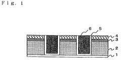
- FIG. 1shows one example of the semiconductor device of the present invention.
- FIGS. 2 a - 2 dshow one example of the method of the present invention for producing a semiconductor device.
- FIGS. 3 a - 3 bshow another example of the method of the present invention for producing a semiconductor device.
- FIG. 4show a multi-layered wiring structure.
- FIG. 5show one example of the conventional semiconductor device.
- FIGS. 6 a - 6 cshow one example of the conventional method for producing a semiconductor device.
- FIGS. 7 a - 7 bshow another example of the conventional method for producing a semiconductor device.
- FIGS. 8 a - 8 bshow still another example of the conventional method for producing a semiconductor device.
- FIGS. 9 a - 9 bshow still another example of the conventional method for producing a semiconductor device.
- FIGS. 10 a - 10 cshow still another example of the method of the present invention for producing a semiconductor device.
- FIGS. 11 a - 11 bshow still another example of the method of the present invention for producing a semiconductor device.
- 1is a silicon nitride film
- 2is an MSQ film
- 3is an MHSQ film
- 4is a silicon oxide film
- 5is a barrier metal film
- 6is a copper film
- 40is a silicon substrate
- 41is an impurity diffusion film
- 42is a gate electrode
- 43is an interlayer connecting plug
- 44is a copper wiring system
- 45is an inter layer insulation film
- 46is a passivation film
- 51is a semiconductor substrate
- 52is a P-type well region
- 53is a field insulation film
- 54is an impurity diffusion film
- 55is a BPSG film
- 57is a contact hole
- 60is a gate electrode
- 61is a silicon oxide film
- 62is a polycrystalline silicon film
- 63is a WSi film
- 64is a silicon nitride film
- 65is a side-wall insulation film
- 72is a polycrystalline silicon film
- 73is
- the first insulation layer for the present inventionis composed of an organic material of low dielectric constant which has a lower dielectric constant than silicon oxide. It preferably has a relative dielectric constant of 3.5 or less, more preferably 3.0 or less, and is suitably composed of an organopolysiloxane or aromatic-containing organic resin.
- the organopolysiloxane useful for the present inventionis a polysiloxane having an organic functional group.
- An alkyl silisesquioxane and hydride alkyl siloxaneare suitably used for their favorable dielectric characteristics and fabricability.
- the suitable compoundsinclude methyl silisesquioxane having the repeating units shown by formulae (I) and (III), and methylated hydrogen silisesquioxane having the repeating units shown by formulae (I), (II) and (III) (hereinafter may be referred to as MHSQ). Of these, methyl silisesquioxane is more preferable for its dielectric characteristics and fabricability.
- the molar ratio of (I) to total of (I), (II) and (III)is preferably 0.5 or more, more preferably 0.7 or more.
- the above ratiois excessively low, it may be difficult to have a sufficiently low dielectric constant and fabricability may be also damaged.
- the aromatic-containing resins useful for the present inventioninclude polyaryl ether (PAE) and divinyl siloxane-bis-benzocyclobutene (BCB). These compounds have a low dielectric constant and relatively good resistance to heat.
- PAEpolyaryl ether
- BCBdivinyl siloxane-bis-benzocyclobutene
- the second insulation layer for the present inventionis composed of a polysiloxane compound having an Si—H group.
- Those polysiloxane compounds suitable for the present inventioninclude hydrogen silisesquioxane having the repeating units shown by formulae (II) and (III), and MHSQ having the repeating units shown by formulae (I), (II) and (III).
- These polymers, having an Si—H group in the moleculesare highly adhesive to the first insulation layer composed of an organic compound of low dielectric constant and to the third layer composed of an inorganic material. The reasons for the excellent adhesion are not fully understood, but it is considered that the Si—H group is dehydrogenated to form the reactive sites, which react with the constituents of the first and third insulation layers.
- the molar ratio of (II) to total of (I), (II) and (III)is preferably 0.2 or more, more preferably 0.5 or more. Sufficient interlayer adhesion can be secured at the ratio in the above range.
- the third insulation layeris provided for the present invention for enhancing resistance to ashing by oxygen plasma while the resist is removed and resistance to scratching during the planarizing process by CMP, and also for preventing increase in dielectric constant, which may be caused by absorbed moisture.
- the third insulation layeris preferably composed of one or more materials selected from the group consisting of silicon oxide, silicon nitride and silicon oxynitride.
- the multi-layered insulation film for the present inventioncontains the first, second and third insulation layers, of which the first layer is preferably thicker than the others, because the present invention tries to effectively utilize the excellent dielectric, planarizing and gap-filling characteristics of the organic material of low constant as the constituent for the first insulation layer.
- the multi-layered insulation film for the present inventionmay have another layer of, e.g., MSQ, placed in the second insulation layer.
- the first insulation layer for the present inventionmay be formed by, e.g., plasma CVD or spin coating.
- the feed gasis a mixture of an alkylsilane gas and oxidizing gas.
- the alkylsilanes useful for the present inventioninclude monomethylsilane, dimethylsilane, trimethylsilane and tetramethylsilane. They may be used either individually or in combination. Of these, trimethylsilane is more preferable.
- the oxidizing gasmeans the gas having the effect of oxidizing the alkylsilane, and has an oxygen atom in the molecule. It may be one or more gases selected from the group consisting of NO, NO 2 , CO, CO 2 and O 2 . Of these, NO and NO 2 are suitably used for their adequate oxidizing power.
- a solution dissolving the layer materialis dropped onto a wafer rotating at a given speed, and thermally treated in two or more stages to be dried and solidified into the film that coats the wafer.
- the second insulation layer for the present inventionmay be formed by, e.g., plasma CVD or spin coating, as is the case with the first insulation layer.
- Plasma CVDis more preferable, when the layer is to be more adhesive.
- the feed gasis a mixture of monosilane (SiH 4 ) gas, an alkylsilane gas and oxidizing gas.
- the alkylsilanes useful for the present inventioninclude monomethylsilane, dimethylsilane, trimethylsilane and tetramethylsilane. They may be used either individually or in combination. Of these, trimethylsilane is more preferable.
- the oxidizing gasmeans the gas having the effect of oxidizing the alkylsilane, and has an oxygen atom in the molecule. It may be one or more gases selected from the group consisting of NO, NO 2 , CO, CO 2 and O 2 . Of these, NO and NO 2 are suitably used for their adequate oxidizing power.
- the first insulation layeris formed by spin coating method
- a solution dissolving the layer materialis dropped onto a wafer rotating at a given speed, and thermally treated in two or more stages to be dried and solidified into the film that coats the wafer.
- the third insulation layer for the present inventionmay be formed by thermal or plasma CVD method.
- the feed gasmay be a mixture of monosilane (SiH 4 ) and an oxidizing gas, or tetraethoxysilane (TEOS), among others.
- first and second insulation layersare formed by the following method (i) or (ii) for the present invention.
- Plasma CVDis employed to form the first and second insulation layers without taking out the semiconductor wafer from the plasma atmosphere.
- a solution containing the organic material of low dielectric constantis spread over the semiconductor wafer by spin coating, and then thermally treated to form the first insulation layer. Then, it is thermally treated at 200° C. or more and 500° C. or less, preferably 350° C. or more and 500° C. or less, before the second insulation layer is provided thereon.
- the semiconductor waferis not taken out from the plasma atmosphere, and hence the Si—H group contained in the second insulation layer is prevented from deteriorating in reactivity.
- the second insulating layer formedis prevented from absorbing moisture, keeping itself particularly adhesive to the other layer.
- the first insulation layeris formed by spin coating which can securely form the insulation material in a narrow space between the gaps. It is therefore suitably applicable to the process of forming the interlayer insulation film on the gate electrode, described in the Prior Art ( FIG. 8 ).
- This methodthermally treats the first insulation layer at a given temperature after it is formed, to make it more adhesive to the second insulation layer. The reasons for improved adhesion are not fully understood, but it is considered that the reactions between the constituents of the first and second layers proceed more smoothly as a result of evaporation of moisture or the like adsorbed on the surface of the first insulation layer and increased reactivity of the first insulation layer surface.
- the thermal treatmentis preferably effected under a vacuum, e.g., 1 to 100 Pa, normally for 1 to 10 minutes.
- the term “wire”generically means anything that electrically connects devices, e.g., transistors, to each other, including word line which also serves as a gate electrode in a memory element.
- the present inventionis particularly effective, when applied to the damascene wiring structure with an electroconductive film filled in a plurality of recesses provided in a multi-layered insulation film and other structures with a self-aligned contact on a gate electrode.
- Example 1describes one example of process flow for producing the semiconductor device with a multi-layered wiring structure with damascene copper wires.
- a multi-layered wiring structure with a plurality of wiring layersis frequently used. It comprises the silicon substrate 40 which supports the transistor composed of the gate electrode 42 and impurity diffusion layer 41 in the first layer (device-forming layer), and two or more interlayer insulation films 45 containing copper wires 44 , connected to each other by interlayer connecting plugs 43 .
- the wiring structure shown in FIG. 1comprises the silicon nitride film 1 , methyl silsesquioxane (MSQ) film 2 , methylated hydrogen silisesquioxane (MHSQ) film 3 and silicon oxide film 4 , formed in this order.
- the multi-layered insulation filmhas two or more wiring grooves, filled with the copper film 6 via the barrier metal film 5 of Ta therein.
- the copper film 6is approximately 200 to 500 nm thick.
- the process for forming the wiring structure shown in FIG. 1is described by referring to the drawings.
- the silicon nitride film 1(thickness: 50 nm) was formed on the lower wiring layer (not shown) by plasma CVD, and then was coated with the MSQ film 2 (thickness: 250 nm).
- the feed gas for forming the MSQ film 2was a mixture of trimethylsilane and N 2 O.
- the MSQ film 2had a structure with the repeating units shown by the formulae (I) and (III).
- the MSQ film 2after its deposition, was then coated with the MHSQ film 3 (thickness: 50 nm) by plasma CVD ( FIG. 2( b )).
- the feed gaswas a mixture of monosilane (SiH 4 ), trimethylsilane and N 2 O.
- the MHSQ film 3had a structure with the repeating units shown by the formulae (I), (II) and (III) above.
- the molar ratio of (II) to total of (I), (II) and (III)is 0.5 to 0.6 from the feed gas composition.
- the MHSQ film 3was then coated with the silicon oxide film 4 (thickness: 100 nm) by plasma CVD or the like ( FIG. 2( c )).
- the feed gaswas a mixture of monosilane (SiH 4 ) and N 2 O.
- the multi-layered film with the laminated MSQ film 2 , MHSQ film 3 and silicon oxide film 4was prepared in a series of steps by changing the feed gas for each film, without taking out the wafer from the plasma atmosphere in the plasma system.
- the multi-layered filmwas then dry-etched to have wiring grooves reaching the silicon nitride film 1 ( FIG. 2( d )).
- Each of the wiring grooveswas coated with the barrier metal film 5 of Ta over the entire surface by sputtering ( FIG. 3( a )) and then with the copper layer 6 also over the entire surface by plating ( FIG. 3( b )).
- the copper film 6may be formed by, e.g., CVD or sputtering, but preferably by plating or CVD for good coverage it gives.
- the entire surfacewas planarized by CMP, to prepare the damascene wiring system while leaving the copper film 6 in each of the wiring grooves.
- the semiconductor device prepared by the above processhad few problems related to crosstalk because the space between the wires was filled with the MSQ film 2 of low dielectric constant, and showed good interlayer adhesion because the MHSQ film 3 was placed between the MSQ film 2 and silicon oxide film 4 .
- the gate electrode 60also serving as the word line was formed on the silicon semiconductor substrate, as shown in FIG. 10( a ).
- the process for forming the above assemblyis described.
- the field insulation film 53was formed by selective oxidation on the surface of the semiconductor substrate 51 composed of p-type single-crystal silicon.
- the phosphorus ionwas implanted to form the p-type well region 52 .
- the silicon oxide film 61was formed by thermal oxidation, and coated with the polycrystalline silicon film 62 , tungsten silicide (WSi) film 63 and silicon oxide film. These films were patterned by etching to form the gate electrode 60 .
- WSitungsten silicide
- the silicon nitride filmwas formed and treated by anisotropic etching, to form the side-wall insulation film 65 of silicon nitride on the side of the gate electrode 60 . Then, ion was implanted to form the impurity diffusion layer 54 . These processes complete the assembly shown in FIG. 10( a ).
- the MSQ film 2(thickness: 300 nm) was formed by spin coating. More concretely, the methyl silsesquioxane solution was dropped onto a rotating wafer provided with the gate electrode patterns. The spin-coated wafer was cured stepwise at 80°, 100° and 120° C., to dry the solvent and solidify the methyl silsesquioxane, and thereby to prepare the MSQ film 2 .
- MSQhas sufficiently good characteristics to fill a narrow gap, and can form the insulation film even in the region provided with the gate electrode patterns at narrow intervals, as shown in FIG. 10( b ).
- the wafer treated to have the MSQ film 2was placed in a film-making device, where it was allowed to stand at 450° C. for around 10 minutes. It was then coated with the MHSQ film 3 (thickness: 50 mm) and silicon oxide film 4 (thickness: 100 nm) by plasma CVD ( FIG. 10( c )).
- the multi-layered structurewas prepared in a series of steps by changing the feed gas for each film, without taking out the wafer from the plasma atmosphere in the plasma device.
- the feed gas for forming the MHSQ film 3was a mixture of monosilane (SiH 4 ), trimethylsilane and N 2 O, and that for forming the silicon oxide film 4 was a mixture of monosilane (SiH 4 ) and N 2 O.
- the molar ratio of the repeating unit (II) to total of the repeating units (I), (II) and (III)was 0.5 to 0.6 from the feed gas composition.
- the multi-layered film with the MSQ film 2 , MHSQ film 3 and silicon oxide film 4was covered with a patterned photoresist (not shown), and the MSQ film 2 , MHSQ film 3 and silicon oxide film 4 were subjected to dry etching with the photoresist serving as the mask, to form the contact hole 57 , during which the side-wall insulation film 65 worked as the etching-stopping film for self-alignment of the contact hole 57 . Then, the film was treated with buffered hydrofluoric acid to remove the natural oxide film on the impurity diffusion layer 54 .
- the polycrystalline silicon film 72was formed in such a way to fill the contact hole 57 , and the phosphorus ion was implanted. Then, the tungsten silicide (WSi) film 73 and silicon oxide film 74 were deposited by DC magnetron sputtering method. Then, the polycrystalline silicon film 72 , the tungsten silicide (WSi) film 73 and silicon oxide film 74 are etched by RIE to form the bit line ( FIG. 11( b ))
- the semiconductor device prepared by the above processhad good gap-filling characteristics because MSQ of good gap-filling and flatness characteristics as a interlayer insulation film, and showed good interlayer adhesion because the MHSQ film 3 was placed between the MSQ film 2 and silicon oxide film 4 .
- the present inventionmay use an organic material of low dielectric constant for the first insulation layer to prevent crosstalk between the wires, and suitably fill the narrow gap by the insulating film material. It has the second insulation layer, composed of a polysiloxane compound having an Si—H group, between the first and third insulation layers to improve the interlayer adhesion, efficiently preventing peeling of these layers from each other.
Landscapes
- Engineering & Computer Science (AREA)
- Physics & Mathematics (AREA)
- Condensed Matter Physics & Semiconductors (AREA)
- General Physics & Mathematics (AREA)
- Computer Hardware Design (AREA)
- Microelectronics & Electronic Packaging (AREA)
- Power Engineering (AREA)
- Manufacturing & Machinery (AREA)
- Internal Circuitry In Semiconductor Integrated Circuit Devices (AREA)
- Formation Of Insulating Films (AREA)
- Chemical Vapour Deposition (AREA)
Abstract
Description
- This Application is a Divisional Application of U.S. patent application Ser. No. 11/797,293, filed on May 2, 2007, which was a Divisional Application of U.S. patent application Ser. No. 10/135,393 (now U.S. Pat. No. 7,229,910) which was filed on May 1, 2002, which was a Divisional Application of U.S. patent application Ser. No. 09/851,313, which was filed on May 9, 2001.
- (1) Field of the Invention
- The present invention relates to a semiconductor wafer on which a film with low dielectric constant is formed, semiconductor device with wires or the like in the above film with low dielectric constant, and methods of producing the same wafer and device.
- (2) Description of the Prior Art
- Recently, techniques for utilizing materials of low dielectric constant, which can decrease inter-wire capacity, have been extensively developed to cope with higher-speed operation of devices.
- A process for forming a damascene copper wiring system of low dielectric constant material is described by referring to
FIGS. 6 and 7 . - Referring to
FIG. 6( a), thesilicon nitride film 1 is formed on the lower wiring layer on the silicon substrate (both not shown), and then is coated with the Methyl Silsesquioxane (MSQ)film 2. TheMSQ film 2 is formed by, e.g., spin coating. It is then coated with thesilicon oxide film 4 of silicon oxide, which works, e.g., to improve resistance to oxygen plasma ashing while the resist used in the subsequent step is separated, and to prevent dielectric constant from increasing in the presence of moisture. The wiring grooves are formed by dry etching in theMSQ film 2 and thesilicon oxide film 4 to reach thesilicon nitride film 1, after thesilicon oxide film 4 is covered with the resist mask (not shown) (FIG. 6( c)). - Next, the entire surface is coated with the
barrier metal film 5 by an adequate method, e.g., sputtering (FIG. 7( a)), and then with thecopper film 6. The surface is then planarized by CMP, while leaving thecopper film 6 in the wiring grooves, to complete the damascene wiring system (FIG. 7( b)). - In the semiconductor device prepared by the above procedure, since the space between the wires is filled with the
MSQ film 2 with low dielectric constant, crosstalk can effectively be prevented. In this device, however, thesilicon oxide film 4 tends to peel off from theorganic MSQ film 2 on which it is formed in the subsequent step as shown inFIG. 5 , because of insufficient adhesion between them at the interface, since the former is of an inorganic material while the latter of an organic material. TheMSQ film 2 will have dielectric constant decreasing as its organic component content increases. On the other hand, thesilicon oxide film 4 is preferably inorganic to have better characteristics, e.g., higher resistance to ashing. Therefore, they tend to be less compatible with each other, leading to peeling at the interface. The peeling causes lowered yield in the wiring step. - An attempt has been made to prevent the peeling by replacing the
MSQ film 2 with a film containing no organic compound, such as that of Hydrogen Silisesquioxane (HSQ). However, the HSQ film has a higher dielectric constant than the MSQ film. - The other measures to prevent the peeling are to treat the MSQ film with ozone, UV-ozone or oxygen plasma, thereby improving its adhesion to the inorganic film. These methods, however, involve problems, e.g., penetration of water into the film, increased dielectric constant of the insulation film, and roughened film surface to leave residue. Therefore, the measures free of the above problems to improve adhesion have been demanded.
- On the other hand, the planarizing process is becoming increasingly important for the interlayer insulation, while the fine machining techniques are required to meet the higher standards. Insufficient flatness will cause various problems, e.g., blurred exposure focus, difficulty in processing photoresist, and increased quantity of residual etchant during the etching process subsequent to masking with the photoresist. In order to make the interlayer insulation film flatter, a material with good reflow characteristics, e.g., BPSG (boron phosphate glass), has been used for the insulation film formed prior to the metal wiring process. The conventional process for forming a memory device or the like incorporating BPSG is described by referring to
FIGS. 8 and 9 . - Referring to
FIG. 8( a), thegate electrode 60 which also serves as the word line is formed on the silicon semiconductor substrate. The processes through which such status is achieved will be described. First, thefield insulation film 53 is formed by selective oxidation on the surface of thesemiconductor substrate 51 composed of p-type single-crystal silicon. Then, the phosphorus ion is implanted to form the p-type well region 52. Then, thesilicon oxide film 61 is formed by thermal oxidation, and coated with thepolycrystalline silicon film 62, tungsten silicide (WSi) film63 and silicon nitride film64. These films are patterned by etching to form thegate electrode 60, Then, the silicon nitride film is formed and treated by anisotropic etching, to form the side-wall insulation film 65 of silicon nitride on the side of thegate electrode 60. Then, ion is implanted to form theimpurity diffusion layer 54. These processes complete the assembly shown inFIG. 8( a). - Then, the BPSG
film 55 is formed by CVD method. It is annealed with nitrogen to reflow, and etched back with buffered hydrogen fluoride (BHF), to planarize theBPSG film 55 surface (FIG. 8( b)). - The
BPSG film 55 surface is covered with a patterned photoresist (not shown), and then subjected to dry etching with the photoresist serving as the mask, to form the contact hole57 (FIG. 9( a)), during which the side-wall insulation film 65 works as the etching-stopping film for self-alignment of thecontact hole 57. Then, the film is treated with buffered hydrofluoric acid to remove the natural oxide film on theimpurity diffusion layer 54. - Then, the
polycrystalline silicon film 72 is formed in such a way to fill thecontact hole 57, and doped with phosphorus. The BPSG film is further coated with the tungsten silicide (WSi)film 73 andsilicon oxide film 74, and etched to form the bit line (FIG. 9( b)). - Recently, the gap between the gate electrodes (word lines) has become very narrow at 0.2 μm or less, to satisfy the requirements for more integration, and the interlayer insulation film material is required to have better gap-filling characteristics. The required gap-filling characteristics become severer for highly integrating processes, such as those described above, which invariably need the so-called self-alignment techniques to secure insulation between the contact hole and wiring layer by the side-wall insulation film of the gate electrode. It is difficult for the conventional processes which use BPSG as the insulation film material to meet these requirements, and use of a material of better gap-filling characteristics is essential. The inorganic SOG films such as HSQ film and organic SOG films such as MSQ film are considered as the ones which can meet the above requirements. However, HSQ is low in resistance to chemical solutions, and difficult to form the contact hole of the shape as designed, because of side etching proceeding during the process of removing the natural oxide film with buffered hydrofluoric acid. The inorganic SOG films other than that of HSQ generally have a disadvantage of being easily cracked. As a result, the organic SOG films, e.g., MSQ film, have been most suitably used. The organic film with low dielectric constant, e.g., MSQ film, has good characteristics of filling a narrow gap, and can secure high flatness.
- When an organic material of low dielectric constant, e.g., MSQ, is used, it is necessarily coated with an inorganic protective film, e.g., silicon oxide film, to have improved characteristics, e.g., resistance to ashing. This will cause the problem of peeling of the inorganic protective film from the MSQ film, as described earlier.
- In consideration of the above-described problems, it is a purpose of the present invention to improve the interfacial adhesion between the film with low dielectric constant and protective film, without damaging the excellent dielectric, flatness and gap-filling characteristics of the organic material of low dielectric constant.
- The present invention for solving the above-described problems may be specified by the following:
- [1] A semiconductor device in which a multi-layered insulation film is formed on a semiconductor substrate and wires are formed in the multi-layered insulation film, characterized in that the multi-layered insulation film comprises a first insulation layer composed of an organic material of low dielectric constant which has a lower dielectric constant than silicon oxide, a second insulation layer composed of a polysiloxane compound having an Si—H group and formed on and being in contact with a top of the first insulation layer, and a third insulation layer composed of an inorganic material and formed on and being in contact with a top of the second insulation layer.
- [2] The semiconductor device according to [1], wherein the first insulation layer is composed of an organopolysiloxane or aromatic-containing organic resin.
- [3] The semiconductor device according to [1] or [2], wherein the second insulation layer is composed of hydrogen silisesquioxane and/or hydride organosiloxane.
- [4] The semiconductor device according to any one of [1] to [3], wherein the third insulation layer is composed of one or more materials selected from the group consisting of silicon oxide, silicon nitride and silicon oxynitride.
- [5] A semiconductor wafer with a multi-layered insulation film formed on one surface of the wafer, characterized in that the multi-layered insulation film comprises a first insulation layer composed of an organic material of low dielectric constant which has a lower dielectric constant than silicon oxide, a second insulation layer composed of a polysiloxane compound having an Si—H group and formed on and being in contact with a top of the first insulation layer, and a third insulation layer composed of an inorganic material and formed on and being in contact with a top of the second insulation layer.
- [6] The semiconductor wafer according to [5], characterized in that the first insulation layer is composed of an organopolysiloxane or aromatic-containing organic resin.
- [7] The semiconductor wafer according to [5] or [6], characterized in that the second insulation layer is composed of hydrogen silisesquioxane and/or hydride organosiloxane.
- [8] The semiconductor wafer according to any one of [5] to [7], characterized in that the third insulation layer is composed of one or more materials selected from the group consisting of silicon oxide, silicon nitride and silicon oxynitride.
- [9] A method of forming a multi-layered insulation film which forms, on a semiconductor wafer, the multi-layered insulation film containing a first insulation layer, a second insulation layer and a third insulation layer, characterized in that the method comprises the steps of forming the first insulation layer composed of an organic material having low dielectric constant which has a lower dielectric constant than silicon oxide, forming the second insulation layer composed of a polysiloxane compound having an Si—H group such that the second insulation layer is in contact with a top of the first insulation layer, and forming third insulation layer composed of an inorganic material such that the third insulation layer is in contact with a top of the second insulation layer.
- [10] The method of forming a multi-layered insulation film according to [9], characterized in that the first insulation layer is composed of an organopolysiloxane or aromatic-containing organic resin.
- [11] The method of forming a multi-layered insulation film according to [9] or [10], characterized in that the second insulation layer is composed of hydrogen silisesquioxane and/or hydride organosiloxane.
- [12] The method of forming a multi-layered insulation film according to any one of [9] to [11], characterized in that the third insulation layer is composed of one or more materials selected from the group consisting of silicon oxide, silicon nitride and silicon oxynitride.
- [13] The method of forming a multi-layered insulation film according to any one of [9] to [12], characterized in that the first and second insulation layers are formed by the plasma CVD method without taking out said semiconductor wafer from the plasma atmosphere.
- [14] The method of forming a multi-layered insulation film according to [13], characterized in that the feed gas for forming the first insulation layer is a mixed gas containing alkylsilane gas and oxidizing gas, and the feed gas for forming the second insulation layer is a mixed gas containing monosilane gas, alkylsilane gas and oxidizing gas.
- [15] The method of forming a multi-layered insulation film according to any one of [9] to [12], characterized in that the semiconductor wafer is spin-coated with a solution containing the organic material of low dielectric constant and then thermally treated to form the first insulation layer, and the first insulation layer is thermally treated in atmosphere at 200° C. or more and 500° C. or less, inclusive, and coated with the second insulation layer by plasma CVD method.
- [16] A method of producing a semiconductor device characterized in that the method comprises steps of forming a first insulation layer composed of an organic material of low dielectric constant which has a lower dielectric constant than silicon oxide, on a semiconductor substrate; forming a second insulation layer composed of a polysiloxane compound having an Si—H group such that the second insulation layer is in contact with a top of the first insulation layer; forming a third insulation layer composed of an inorganic material such that the third insulation layer is in contact with a top of the second insulation layer; etching the first, second and third insulation layers to form recesses therein; forming an electroconductive film over the entire surfaces of these recesses in such a way to fill them; and removing the electroconductive film formed on the region outside of each of these recesses by chemical mechanical polishing or etching.
- [17] A method of producing a semiconductor device characterized in that the method comprises steps of forming, on a semiconductor substrate, a gate electrode with a side-wall insulation layer provided on its side, and a pair of impurity diffusion regions in the surface area of the semiconductor substrate on both sides of the gate electrode; forming a first insulation layer composed of an organic material of low dielectric constant which has a lower dielectric constant than silicon oxide, over the entire surface; forming a second insulation layer composed of a polysiloxane compound having an Si—H group such that the second insulation layer is in contact with a top of the first insulation layer; forming a third insulation layer composed of an inorganic material such that the third insulation layer is in contact with a top of the second insulation layer; etching the first, second and third insulation layers to form a contact hole, exposing the impurity diffusion regions to the bottom of the contact hole, and exposing the side-wall insulation layer to the side of the contact hole; and forming an electroconductive film over the entire surface in such a way to fill the contact hole.
- [18] The method of producing a semiconductor device according to [16] or [17], characterized in that the first insulation layer is composed of an organopolysiloxane or aromatic-containing organic resin.
- [19] The method of producing a semiconductor device according to any one of [16] to [18], characterized in that the second insulation layer is composed of hydrogen silisesquioxane and/or hydride organosiloxane.
- [20] The method of producing a semiconductor device according to any one of [16] to [19], characterized in that the third insulation layer is composed of one or more materials selected from the group consisting of silicon oxide, silicon nitride and silicon oxynitride.
- [21] The method of producing a semiconductor device according to any one of [16] to [20], characterized in that the first and second insulation layers are formed by the plasma CVD method without taking out said semiconductor wafer from the plasma atmosphere.
- [22] The method of producing a semiconductor device according to [21], characterized in that the feed gas for forming the first insulation layer is a mixed gas containing alkylsilane gas and oxidizing gas, and the feed gas for forming the second insulation layer is a mixed gas containing monosilane gas, alkylsilane gas and oxidizing gas.
- [23] The method of producing a semiconductor device according to any one of [16] to [20], characterized in that the semiconductor wafer is spin-coated with a solution containing the organic material of low dielectric constant and then thermally treated to form the first insulation layer, and the first insulation layer is thermally treated in atmosphere at 200° C. or more and 500° C. or less, inclusive, and coated with the second insulation layer by plasma CVD method.
- The present invention described above, using an organic material of low dielectric constant for the first insulation layer, thus may prevent crosstalk between the wires, and suitably fill the narrow gap by the insulating film material. It has the second insulation layer, composed of a polysiloxane compound having an Si—H group, between the first and third insulation layers to improve the interlayer adhesion, efficiently preventing peeling of these layers from each other. These features improve process yield and provide the semiconductor device with high reliability.
- The recess in the method [16] of the present invention may take any feature, including wiring groove or contact hole. In the method [17] of the present invention, the ion implanting for forming the impurity diffusion region is effected after the gate electrode patterns are formed, but may be effected either before or after the side-wall insulation film is formed.
FIG. 1 shows one example of the semiconductor device of the present invention.FIGS. 2 a-2dshow one example of the method of the present invention for producing a semiconductor device.FIGS. 3 a-3bshow another example of the method of the present invention for producing a semiconductor device.FIG. 4 show a multi-layered wiring structure.FIG. 5 show one example of the conventional semiconductor device.FIGS. 6 a-6cshow one example of the conventional method for producing a semiconductor device.FIGS. 7 a-7bshow another example of the conventional method for producing a semiconductor device.FIGS. 8 a-8bshow still another example of the conventional method for producing a semiconductor device.FIGS. 9 a-9bshow still another example of the conventional method for producing a semiconductor device.FIGS. 10 a-10cshow still another example of the method of the present invention for producing a semiconductor device.FIGS. 11 a-11bshow still another example of the method of the present invention for producing a semiconductor device.- In these figures,1 is a silicon nitride film,2 is an MSQ film,3 is an MHSQ film,4 is a silicon oxide film,5 is a barrier metal film,6 is a copper film,40 is a silicon substrate,41 is an impurity diffusion film,42 is a gate electrode,43 is an interlayer connecting plug,44 is a copper wiring system,45 is an inter layer insulation film,46 is a passivation film,51 is a semiconductor substrate,52 is a P-type well region,53 is a field insulation film,54 is an impurity diffusion film,55 is a BPSG film,57 is a contact hole,60 is a gate electrode,61 is a silicon oxide film,62 is a polycrystalline silicon film,63 is a WSi film,64 is a silicon nitride film,65 is a side-wall insulation film,72 is a polycrystalline silicon film,73 is a tungsten silicide film and74 is a silicon oxide film.
- The first insulation layer for the present invention is composed of an organic material of low dielectric constant which has a lower dielectric constant than silicon oxide. It preferably has a relative dielectric constant of 3.5 or less, more preferably 3.0 or less, and is suitably composed of an organopolysiloxane or aromatic-containing organic resin.
- The organopolysiloxane useful for the present invention is a polysiloxane having an organic functional group. An alkyl silisesquioxane and hydride alkyl siloxane are suitably used for their favorable dielectric characteristics and fabricability. The suitable compounds include methyl silisesquioxane having the repeating units shown by formulae (I) and (III), and methylated hydrogen silisesquioxane having the repeating units shown by formulae (I), (II) and (III) (hereinafter may be referred to as MHSQ). Of these, methyl silisesquioxane is more preferable for its dielectric characteristics and fabricability.
- When MHSQ is used, the molar ratio of (I) to total of (I), (II) and (III) is preferably 0.5 or more, more preferably 0.7 or more. When the above ratio is excessively low, it may be difficult to have a sufficiently low dielectric constant and fabricability may be also damaged.
- The aromatic-containing resins useful for the present invention include polyaryl ether (PAE) and divinyl siloxane-bis-benzocyclobutene (BCB). These compounds have a low dielectric constant and relatively good resistance to heat.
- The second insulation layer for the present invention is composed of a polysiloxane compound having an Si—H group. Those polysiloxane compounds suitable for the present invention include hydrogen silisesquioxane having the repeating units shown by formulae (II) and (III), and MHSQ having the repeating units shown by formulae (I), (II) and (III). These polymers, having an Si—H group in the molecules, are highly adhesive to the first insulation layer composed of an organic compound of low dielectric constant and to the third layer composed of an inorganic material. The reasons for the excellent adhesion are not fully understood, but it is considered that the Si—H group is dehydrogenated to form the reactive sites, which react with the constituents of the first and third insulation layers.
- When MHSQ is used, the molar ratio of (II) to total of (I), (II) and (III) is preferably 0.2 or more, more preferably 0.5 or more. Sufficient interlayer adhesion can be secured at the ratio in the above range.
- The third insulation layer is provided for the present invention for enhancing resistance to ashing by oxygen plasma while the resist is removed and resistance to scratching during the planarizing process by CMP, and also for preventing increase in dielectric constant, which may be caused by absorbed moisture. The third insulation layer is preferably composed of one or more materials selected from the group consisting of silicon oxide, silicon nitride and silicon oxynitride.
- The multi-layered insulation film for the present invention contains the first, second and third insulation layers, of which the first layer is preferably thicker than the others, because the present invention tries to effectively utilize the excellent dielectric, planarizing and gap-filling characteristics of the organic material of low constant as the constituent for the first insulation layer. The multi-layered insulation film for the present invention may have another layer of, e.g., MSQ, placed in the second insulation layer.
- The first insulation layer for the present invention may be formed by, e.g., plasma CVD or spin coating. When plasma CVD is employed, the feed gas is a mixture of an alkylsilane gas and oxidizing gas. The alkylsilanes useful for the present invention include monomethylsilane, dimethylsilane, trimethylsilane and tetramethylsilane. They may be used either individually or in combination. Of these, trimethylsilane is more preferable.
- The oxidizing gas means the gas having the effect of oxidizing the alkylsilane, and has an oxygen atom in the molecule. It may be one or more gases selected from the group consisting of NO, NO2, CO, CO2and O2. Of these, NO and NO2are suitably used for their adequate oxidizing power. When the first insulation layer is formed by spin coating, on the other hand, a solution dissolving the layer material is dropped onto a wafer rotating at a given speed, and thermally treated in two or more stages to be dried and solidified into the film that coats the wafer.
- The second insulation layer for the present invention may be formed by, e.g., plasma CVD or spin coating, as is the case with the first insulation layer. Plasma CVD is more preferable, when the layer is to be more adhesive.
- When plasma CVD method is employed, the feed gas is a mixture of monosilane (SiH4) gas, an alkylsilane gas and oxidizing gas. The alkylsilanes useful for the present invention include monomethylsilane, dimethylsilane, trimethylsilane and tetramethylsilane. They may be used either individually or in combination. Of these, trimethylsilane is more preferable. The oxidizing gas means the gas having the effect of oxidizing the alkylsilane, and has an oxygen atom in the molecule. It may be one or more gases selected from the group consisting of NO, NO2, CO, CO2and O2. Of these, NO and NO2are suitably used for their adequate oxidizing power.
- When the first insulation layer is formed by spin coating method, on the other hand, a solution dissolving the layer material is dropped onto a wafer rotating at a given speed, and thermally treated in two or more stages to be dried and solidified into the film that coats the wafer.
- The third insulation layer for the present invention may be formed by thermal or plasma CVD method. The feed gas may be a mixture of monosilane (SiH4) and an oxidizing gas, or tetraethoxysilane (TEOS), among others.
- It is preferable to form the first and second insulation layers by the following method (i) or (ii) for the present invention.
- (i) Plasma CVD is employed to form the first and second insulation layers without taking out the semiconductor wafer from the plasma atmosphere.
- (ii) A solution containing the organic material of low dielectric constant is spread over the semiconductor wafer by spin coating, and then thermally treated to form the first insulation layer. Then, it is thermally treated at 200° C. or more and 500° C. or less, preferably 350° C. or more and 500° C. or less, before the second insulation layer is provided thereon.
- In the method (i), the semiconductor wafer is not taken out from the plasma atmosphere, and hence the Si—H group contained in the second insulation layer is prevented from deteriorating in reactivity. At the same time, the second insulating layer formed is prevented from absorbing moisture, keeping itself particularly adhesive to the other layer.
- In the method (ii), the first insulation layer is formed by spin coating which can securely form the insulation material in a narrow space between the gaps. It is therefore suitably applicable to the process of forming the interlayer insulation film on the gate electrode, described in the Prior Art (
FIG. 8 ). This method thermally treats the first insulation layer at a given temperature after it is formed, to make it more adhesive to the second insulation layer. The reasons for improved adhesion are not fully understood, but it is considered that the reactions between the constituents of the first and second layers proceed more smoothly as a result of evaporation of moisture or the like adsorbed on the surface of the first insulation layer and increased reactivity of the first insulation layer surface. The thermal treatment is preferably effected under a vacuum, e.g., 1 to 100 Pa, normally for 1 to 10 minutes. - In the present invention, the term “wire” generically means anything that electrically connects devices, e.g., transistors, to each other, including word line which also serves as a gate electrode in a memory element. The present invention is particularly effective, when applied to the damascene wiring structure with an electroconductive film filled in a plurality of recesses provided in a multi-layered insulation film and other structures with a self-aligned contact on a gate electrode.
- Example 1 describes one example of process flow for producing the semiconductor device with a multi-layered wiring structure with damascene copper wires.
- In a logic device or the like, a multi-layered wiring structure with a plurality of wiring layers, such as the one shown in
FIG. 4 , is frequently used. It comprises thesilicon substrate 40 which supports the transistor composed of thegate electrode 42 andimpurity diffusion layer 41 in the first layer (device-forming layer), and two or moreinterlayer insulation films 45 containingcopper wires 44, connected to each other by interlayer connecting plugs43. - This example adopts the wiring layer shown in detail in
FIG. 1 as the component of the multi-layered wiring system. The wiring structure shown inFIG. 1 comprises thesilicon nitride film 1, methyl silsesquioxane (MSQ)film 2, methylated hydrogen silisesquioxane (MHSQ)film 3 andsilicon oxide film 4, formed in this order. The multi-layered insulation film has two or more wiring grooves, filled with thecopper film 6 via thebarrier metal film 5 of Ta therein. Thecopper film 6 is approximately 200 to 500 nm thick. - The process for forming the wiring structure shown in
FIG. 1 is described by referring to the drawings. Referring toFIG. 2( a), the silicon nitride film1 (thickness: 50 nm) was formed on the lower wiring layer (not shown) by plasma CVD, and then was coated with the MSQ film2 (thickness: 250 nm). The feed gas for forming theMSQ film 2 was a mixture of trimethylsilane and N2O. TheMSQ film 2 had a structure with the repeating units shown by the formulae (I) and (III). - The
MSQ film 2, after its deposition, was then coated with the MHSQ film3 (thickness: 50 nm) by plasma CVD (FIG. 2( b)). The feed gas was a mixture of monosilane (SiH4), trimethylsilane and N2O. TheMHSQ film 3 had a structure with the repeating units shown by the formulae (I), (II) and (III) above. The molar ratio of (II) to total of (I), (II) and (III) is 0.5 to 0.6 from the feed gas composition. - The
MHSQ film 3 was then coated with the silicon oxide film4 (thickness: 100 nm) by plasma CVD or the like (FIG. 2( c)). The feed gas was a mixture of monosilane (SiH4) and N2O. - Thus, the multi-layered film with the
laminated MSQ film 2,MHSQ film 3 andsilicon oxide film 4 was prepared in a series of steps by changing the feed gas for each film, without taking out the wafer from the plasma atmosphere in the plasma system. The multi-layered film was then dry-etched to have wiring grooves reaching the silicon nitride film1 (FIG. 2( d)). - Each of the wiring grooves was coated with the
barrier metal film 5 of Ta over the entire surface by sputtering (FIG. 3( a)) and then with thecopper layer 6 also over the entire surface by plating (FIG. 3( b)). Thecopper film 6 may be formed by, e.g., CVD or sputtering, but preferably by plating or CVD for good coverage it gives. On completion of formation of thecopper film 6, the entire surface was planarized by CMP, to prepare the damascene wiring system while leaving thecopper film 6 in each of the wiring grooves. - The semiconductor device prepared by the above process had few problems related to crosstalk because the space between the wires was filled with the
MSQ film 2 of low dielectric constant, and showed good interlayer adhesion because theMHSQ film 3 was placed between theMSQ film 2 andsilicon oxide film 4. - The
gate electrode 60 also serving as the word line was formed on the silicon semiconductor substrate, as shown inFIG. 10( a). The process for forming the above assembly is described. First, thefield insulation film 53 was formed by selective oxidation on the surface of thesemiconductor substrate 51 composed of p-type single-crystal silicon. Then, the phosphorus ion was implanted to form the p-type well region 52. Then, thesilicon oxide film 61 was formed by thermal oxidation, and coated with thepolycrystalline silicon film 62, tungsten silicide (WSi) film63 and silicon oxide film. These films were patterned by etching to form thegate electrode 60. Then, the silicon nitride film was formed and treated by anisotropic etching, to form the side-wall insulation film 65 of silicon nitride on the side of thegate electrode 60. Then, ion was implanted to form theimpurity diffusion layer 54. These processes complete the assembly shown inFIG. 10( a). - Then, the MSQ film2 (thickness: 300 nm) was formed by spin coating. More concretely, the methyl silsesquioxane solution was dropped onto a rotating wafer provided with the gate electrode patterns. The spin-coated wafer was cured stepwise at 80°, 100° and 120° C., to dry the solvent and solidify the methyl silsesquioxane, and thereby to prepare the
MSQ film 2. MSQ has sufficiently good characteristics to fill a narrow gap, and can form the insulation film even in the region provided with the gate electrode patterns at narrow intervals, as shown inFIG. 10( b). - The wafer treated to have the
MSQ film 2 was placed in a film-making device, where it was allowed to stand at 450° C. for around 10 minutes. It was then coated with the MHSQ film3 (thickness: 50 mm) and silicon oxide film4 (thickness: 100 nm) by plasma CVD (FIG. 10( c)). The multi-layered structure was prepared in a series of steps by changing the feed gas for each film, without taking out the wafer from the plasma atmosphere in the plasma device. The feed gas for forming theMHSQ film 3 was a mixture of monosilane (SiH4), trimethylsilane and N2O, and that for forming thesilicon oxide film 4 was a mixture of monosilane (SiH4) and N2O. The molar ratio of the repeating unit (II) to total of the repeating units (I), (II) and (III) was 0.5 to 0.6 from the feed gas composition. - The multi-layered film with the
MSQ film 2,MHSQ film 3 andsilicon oxide film 4 was covered with a patterned photoresist (not shown), and theMSQ film 2,MHSQ film 3 andsilicon oxide film 4 were subjected to dry etching with the photoresist serving as the mask, to form thecontact hole 57, during which the side-wall insulation film 65 worked as the etching-stopping film for self-alignment of thecontact hole 57. Then, the film was treated with buffered hydrofluoric acid to remove the natural oxide film on theimpurity diffusion layer 54. - The
polycrystalline silicon film 72 was formed in such a way to fill thecontact hole 57, and the phosphorus ion was implanted. Then, the tungsten silicide (WSi)film 73 andsilicon oxide film 74 were deposited by DC magnetron sputtering method. Then, thepolycrystalline silicon film 72, the tungsten silicide (WSi)film 73 andsilicon oxide film 74 are etched by RIE to form the bit line (FIG. 11( b)) - The semiconductor device prepared by the above process had good gap-filling characteristics because MSQ of good gap-filling and flatness characteristics as a interlayer insulation film, and showed good interlayer adhesion because the
MHSQ film 3 was placed between theMSQ film 2 andsilicon oxide film 4. - As described above, the present invention may use an organic material of low dielectric constant for the first insulation layer to prevent crosstalk between the wires, and suitably fill the narrow gap by the insulating film material. It has the second insulation layer, composed of a polysiloxane compound having an Si—H group, between the first and third insulation layers to improve the interlayer adhesion, efficiently preventing peeling of these layers from each other.


Claims (8)

Priority Applications (1)
| Application Number | Priority Date | Filing Date | Title |
|---|---|---|---|
| US12/320,053US7816280B2 (en) | 2000-05-16 | 2009-01-15 | Semiconductor device, semiconductor wafer, and methods of producing the same device and wafer |
Applications Claiming Priority (6)
| Application Number | Priority Date | Filing Date | Title |
|---|---|---|---|
| JP2000143725AJP4368498B2 (en) | 2000-05-16 | 2000-05-16 | Semiconductor device, semiconductor wafer and manufacturing method thereof |
| JP2000-143725 | 2000-05-16 | ||
| US09/851,313US7602048B2 (en) | 2000-05-16 | 2001-05-09 | Semiconductor device and semiconductor wafer having a multi-layered insulation film |
| US10/135,393US7229910B2 (en) | 2000-05-16 | 2002-05-01 | Method of producing a semiconductor device having a multi-layered insulation film |
| US11/797,293US7674721B2 (en) | 2000-05-16 | 2007-05-02 | Semiconductor device, semiconductor wafer, and methods of producing same device and wafer |
| US12/320,053US7816280B2 (en) | 2000-05-16 | 2009-01-15 | Semiconductor device, semiconductor wafer, and methods of producing the same device and wafer |
Related Parent Applications (1)
| Application Number | Title | Priority Date | Filing Date |
|---|---|---|---|
| US11/797,293DivisionUS7674721B2 (en) | 2000-05-16 | 2007-05-02 | Semiconductor device, semiconductor wafer, and methods of producing same device and wafer |
Publications (2)
| Publication Number | Publication Date |
|---|---|
| US20090137108A1true US20090137108A1 (en) | 2009-05-28 |
| US7816280B2 US7816280B2 (en) | 2010-10-19 |
Family
ID=18650501
Family Applications (4)
| Application Number | Title | Priority Date | Filing Date |
|---|---|---|---|
| US09/851,313Expired - Fee RelatedUS7602048B2 (en) | 2000-05-16 | 2001-05-09 | Semiconductor device and semiconductor wafer having a multi-layered insulation film |
| US10/135,393Expired - LifetimeUS7229910B2 (en) | 2000-05-16 | 2002-05-01 | Method of producing a semiconductor device having a multi-layered insulation film |
| US11/797,293Expired - Fee RelatedUS7674721B2 (en) | 2000-05-16 | 2007-05-02 | Semiconductor device, semiconductor wafer, and methods of producing same device and wafer |
| US12/320,053Expired - Fee RelatedUS7816280B2 (en) | 2000-05-16 | 2009-01-15 | Semiconductor device, semiconductor wafer, and methods of producing the same device and wafer |
Family Applications Before (3)
| Application Number | Title | Priority Date | Filing Date |
|---|---|---|---|
| US09/851,313Expired - Fee RelatedUS7602048B2 (en) | 2000-05-16 | 2001-05-09 | Semiconductor device and semiconductor wafer having a multi-layered insulation film |
| US10/135,393Expired - LifetimeUS7229910B2 (en) | 2000-05-16 | 2002-05-01 | Method of producing a semiconductor device having a multi-layered insulation film |
| US11/797,293Expired - Fee RelatedUS7674721B2 (en) | 2000-05-16 | 2007-05-02 | Semiconductor device, semiconductor wafer, and methods of producing same device and wafer |
Country Status (3)
| Country | Link |
|---|---|
| US (4) | US7602048B2 (en) |
| JP (1) | JP4368498B2 (en) |
| TW (1) | TW495882B (en) |
Families Citing this family (40)
| Publication number | Priority date | Publication date | Assignee | Title |
|---|---|---|---|---|
| US6156743A (en)* | 1999-10-18 | 2000-12-05 | Whitcomb; John E. | Method of decreasing fatigue |
| JP4368498B2 (en)* | 2000-05-16 | 2009-11-18 | Necエレクトロニクス株式会社 | Semiconductor device, semiconductor wafer and manufacturing method thereof |
| CN101810521B (en)* | 2001-08-27 | 2015-05-13 | 辛尼科有限责任公司 | Satiation devices and methods |
| US7097665B2 (en)* | 2003-01-16 | 2006-08-29 | Synecor, Llc | Positioning tools and methods for implanting medical devices |
| US6675809B2 (en)* | 2001-08-27 | 2004-01-13 | Richard S. Stack | Satiation devices and methods |
| US7146984B2 (en)* | 2002-04-08 | 2006-12-12 | Synecor, Llc | Method and apparatus for modifying the exit orifice of a satiation pouch |
| US20040033371A1 (en)* | 2002-05-16 | 2004-02-19 | Hacker Nigel P. | Deposition of organosilsesquioxane films |
| US6933568B2 (en) | 2002-05-17 | 2005-08-23 | Samsung Electronics Co., Ltd. | Deposition method of insulating layers having low dielectric constant of semiconductor device, a thin film transistor substrate using the same and a method of manufacturing the same |
| US7018678B2 (en)* | 2002-06-03 | 2006-03-28 | Shipley Company, L.L.C. | Electronic device manufacture |
| SE521977C2 (en)* | 2002-06-20 | 2003-12-23 | Mobile Media Group Stockholm A | Method and apparatus for formatting a web service |
| US7569497B2 (en)* | 2002-07-30 | 2009-08-04 | Tokyo Electron Limited | Method and apparatus for forming insulating layer |
| DE10237787A1 (en)* | 2002-08-17 | 2004-03-04 | Robert Bosch Gmbh | Layer system with a silicon layer and a passivation layer, method for producing a passivation layer on a silicon layer and their use |
| JP2004095865A (en)* | 2002-08-30 | 2004-03-25 | Nec Electronics Corp | Semiconductor device and manufacturing method therefor |
| JP3676784B2 (en) | 2003-01-28 | 2005-07-27 | Necエレクトロニクス株式会社 | Semiconductor device and manufacturing method thereof |
| JP2004235548A (en) | 2003-01-31 | 2004-08-19 | Nec Electronics Corp | Semiconductor device and its fabricating method |
| TW200512926A (en)* | 2003-09-18 | 2005-04-01 | Semiconductor Leading Edge Tec | Method of manufacturing semiconductor device |
| JP4864307B2 (en)* | 2003-09-30 | 2012-02-01 | アイメック | Method for selectively forming an air gap and apparatus obtained by the method |
| US20050247320A1 (en)* | 2003-10-10 | 2005-11-10 | Stack Richard S | Devices and methods for retaining a gastro-esophageal implant |
| JP4434146B2 (en) | 2003-11-28 | 2010-03-17 | 日本電気株式会社 | Porous insulating film, method of manufacturing the same, and semiconductor device using the porous insulating film |
| JP4676694B2 (en)* | 2003-12-15 | 2011-04-27 | ルネサスエレクトロニクス株式会社 | Multilayer structure, semiconductor device and manufacturing method thereof |
| JP4938222B2 (en) | 2004-02-03 | 2012-05-23 | ルネサスエレクトロニクス株式会社 | Semiconductor device |
| WO2005105003A1 (en) | 2004-04-26 | 2005-11-10 | Synecor, Llc | Restrictive and/or obstructive implant for inducing weight loss |
| KR100549014B1 (en)* | 2004-07-21 | 2006-02-02 | 삼성전자주식회사 | Semiconductor Devices Having A Spacer Pattern And Methods Of Forming The Same |
| US7396769B2 (en)* | 2004-08-02 | 2008-07-08 | Lam Research Corporation | Method for stripping photoresist from etched wafer |
| US7504470B2 (en)* | 2004-08-31 | 2009-03-17 | Silecs Oy | Polyorganosiloxane dielectric materials |
| KR100685734B1 (en)* | 2005-06-07 | 2007-02-26 | 삼성전자주식회사 | Porous spin on glass composition, preparation method thereof and method for manufacturing porous silicon oxide film using same |
| JP2007036067A (en)* | 2005-07-28 | 2007-02-08 | Sony Corp | Method for manufacturing semiconductor device |
| US20080190989A1 (en)* | 2005-10-03 | 2008-08-14 | Crews Samuel T | Endoscopic plication device and method |
| US9314361B2 (en)* | 2006-09-15 | 2016-04-19 | Boston Scientific Scimed, Inc. | System and method for anchoring stomach implant |
| TWI345811B (en)* | 2007-08-22 | 2011-07-21 | Vanguard Int Semiconduct Corp | A method of fabricating a semiconductor device |
| US7934631B2 (en) | 2008-11-10 | 2011-05-03 | Barosense, Inc. | Multi-fire stapling systems and methods for delivering arrays of staples |
| EP2571427B1 (en) | 2010-05-21 | 2017-07-19 | Boston Scientific Scimed, Inc. | Tissue-acquisition and fastening devices |
| US10544330B2 (en)* | 2017-01-20 | 2020-01-28 | Honeywell International Inc. | Gap filling dielectric materials |
| US10170301B2 (en) | 2017-03-29 | 2019-01-01 | International Business Machines Corporation | Adhesion of polymers on silicon substrates |
| KR102650216B1 (en) | 2018-03-09 | 2024-03-21 | 삼성전자주식회사 | Method of forming oxide layer and method of fabricating semiconductor device |
| US11239155B2 (en)* | 2019-12-22 | 2022-02-01 | Intel Corporation | Conductive contact structures for electrostatic discharge protection in integrated circuits |
| US12113279B2 (en)* | 2020-09-22 | 2024-10-08 | Oti Lumionics Inc. | Device incorporating an IR signal transmissive region |
| KR20250139404A (en) | 2020-12-07 | 2025-09-23 | 오티아이 루미오닉스 인크. | Patterning a conductive deposited layer using a nucleation inhibiting coating and an underlying metallic coating |
| US20250057035A1 (en)* | 2021-12-14 | 2025-02-13 | Oti Lumionics Inc. | Opto-electronic device comprising a patterning coating comprising a plurality of materials |
| CN120261401B (en)* | 2025-05-30 | 2025-09-26 | 合肥晶合集成电路股份有限公司 | Semiconductor structure and method for manufacturing the same |
Citations (41)
| Publication number | Priority date | Publication date | Assignee | Title |
|---|---|---|---|---|
| US4382057A (en)* | 1981-12-04 | 1983-05-03 | General Electric Company | Silicone rubber compositions for liquid injection molding machines |
| US5672660A (en)* | 1995-12-01 | 1997-09-30 | Advanced Elastomer Systems, L.P. | Hydrosilylation crosslinking |
| US5818111A (en)* | 1997-03-21 | 1998-10-06 | Texas Instruments Incorporated | Low capacitance interconnect structures in integrated circuits using a stack of low dielectric materials |
| US6001747A (en)* | 1998-07-22 | 1999-12-14 | Vlsi Technology, Inc. | Process to improve adhesion of cap layers in integrated circuits |
| US6051508A (en)* | 1997-09-09 | 2000-04-18 | Kabushiki Kaisha Toshiba | Manufacturing method of semiconductor device |
| US6054379A (en)* | 1998-02-11 | 2000-04-25 | Applied Materials, Inc. | Method of depositing a low k dielectric with organo silane |
| US6080526A (en)* | 1997-03-24 | 2000-06-27 | Alliedsignal Inc. | Integration of low-k polymers into interlevel dielectrics using controlled electron-beam radiation |
| US6124641A (en)* | 1997-06-26 | 2000-09-26 | Mitsubishi Denki Kabushiki Kaisha | Semiconductor device organic insulator film |
| US6168726B1 (en)* | 1998-11-25 | 2001-01-02 | Applied Materials, Inc. | Etching an oxidized organo-silane film |
| US6191028B1 (en)* | 1997-12-03 | 2001-02-20 | United Microelectronics, Corp | Method of patterning dielectric |
| US6197703B1 (en)* | 1998-08-17 | 2001-03-06 | Advanced Micro Devices, Inc. | Apparatus and method for manufacturing semiconductors using low dielectric constant materials |
| US6248704B1 (en)* | 1999-05-03 | 2001-06-19 | Ekc Technology, Inc. | Compositions for cleaning organic and plasma etched residues for semiconductors devices |
| US20010005546A1 (en)* | 1998-02-11 | 2001-06-28 | Applied Materials, Inc. | Plasma processes for depositing low dielectric constant films |
| US6274497B1 (en)* | 1999-11-25 | 2001-08-14 | Taiwan Semiconductor Manufacturing Co., Ltd. | Copper damascene manufacturing process |
| US6277732B1 (en)* | 1999-05-26 | 2001-08-21 | Taiwan Semiconductor Manufacturing Co., Ltd. | Method of planarizing inter-metal dielectric layer |
| US6284675B1 (en)* | 1998-05-27 | 2001-09-04 | Texas Instruments Incorporated | Method of forming integrated circuit dielectric by evaporating solvent to yield phase separation |
| US6287951B1 (en)* | 1998-12-07 | 2001-09-11 | Motorola Inc. | Process for forming a combination hardmask and antireflective layer |
| US6303192B1 (en)* | 1998-07-22 | 2001-10-16 | Philips Semiconductor Inc. | Process to improve adhesion of PECVD cap layers in integrated circuits |
| US6323121B1 (en)* | 2000-05-12 | 2001-11-27 | Taiwan Semiconductor Manufacturing Company | Fully dry post-via-etch cleaning method for a damascene process |
| US6326692B1 (en)* | 2000-02-23 | 2001-12-04 | Advanced Micro Devices, Inc. | Insulating and capping structure with preservation of the low dielectric constant of the insulating layer |
| US6333257B1 (en)* | 1998-02-26 | 2001-12-25 | Matsushita Electric Industrial Co., Ltd. | Interconnection structure and method for forming the same |
| US6383951B1 (en)* | 1998-09-03 | 2002-05-07 | Micron Technology, Inc. | Low dielectric constant material for integrated circuit fabrication |
| US6403471B1 (en)* | 1999-10-02 | 2002-06-11 | Taiwan Semiconductor Manufacturing Co., Ltd. | Method of forming a dual damascene structure including smoothing the top part of a via |
| US6407011B1 (en)* | 1999-07-27 | 2002-06-18 | Sony Corporation | Low dielectric constant insulating films with laminated carbon-containing silicon oxide and organic layers |
| US6423652B1 (en)* | 1999-09-27 | 2002-07-23 | United Microelectronics Corp. | Post-processing treatment of low dielectric constant material |
| US6426249B1 (en)* | 2000-03-16 | 2002-07-30 | International Business Machines Corporation | Buried metal dual damascene plate capacitor |
| US6429147B2 (en)* | 1997-06-30 | 2002-08-06 | Sony Corporation | Method for making an insulating film |
| US6448655B1 (en)* | 1998-04-28 | 2002-09-10 | International Business Machines Corporation | Stabilization of fluorine-containing low-k dielectrics in a metal/insulator wiring structure by ultraviolet irradiation |
| US6448186B1 (en)* | 2000-10-06 | 2002-09-10 | Novellus Systems, Inc. | Method and apparatus for use of hydrogen and silanes in plasma |
| US6452274B1 (en)* | 1997-11-17 | 2002-09-17 | Sony Corporation | Semiconductor device having a low dielectric layer as an interlayer insulating layer |
| US20020137359A1 (en)* | 2000-10-25 | 2002-09-26 | International Business Machines Corporation | Ultralow dielectric constant material as an intralevel or interlevel dielectric in a semiconductor device and electronic device containing the same |
| US20020140101A1 (en)* | 2001-03-27 | 2002-10-03 | Advanced Micro Devices, Inc. | Stabilizing fluorine etching of low-k materials |
| US6465361B1 (en)* | 2001-02-20 | 2002-10-15 | Advanced Micro Devices, Inc. | Method for preventing damage of low-k dielectrics during patterning |
| US6476132B1 (en)* | 1999-07-23 | 2002-11-05 | Advanced Elastomer Systems, L.P. | Use of a silane grafted polyolefin in EPDM/polyolefin thermoplastic vulcanizates to improve compression set |
| US6485815B1 (en)* | 1999-05-24 | 2002-11-26 | Samsung Electronics Co., Ltd. | Multi-layered dielectric layer including insulating layer having Si-CH3 bond therein and method for fabricating the same |
| US6624061B2 (en)* | 1998-05-28 | 2003-09-23 | Nec Electronics Corporation | Semiconductor device and method of manufacturing the same capable of reducing deterioration of low dielectric constant film |
| US6627539B1 (en)* | 1998-05-29 | 2003-09-30 | Newport Fab, Llc | Method of forming dual-damascene interconnect structures employing low-k dielectric materials |
| US6800928B1 (en)* | 1997-05-28 | 2004-10-05 | Texas Instruments Incorporated | Porous integrated circuit dielectric with decreased surface porosity |
| US6812161B2 (en)* | 1998-07-28 | 2004-11-02 | Imec Vzw | Method of manufacturing surface textured high-efficiency radiating devices and devices obtained therefrom |
| US20050233591A1 (en)* | 2004-03-31 | 2005-10-20 | Applied Materials, Inc. | Techniques promoting adhesion of porous low K film to underlying barrier layer |
| US7229910B2 (en)* | 2000-05-16 | 2007-06-12 | Nec Electronics Corporation | Method of producing a semiconductor device having a multi-layered insulation film |
Family Cites Families (16)
| Publication number | Priority date | Publication date | Assignee | Title |
|---|---|---|---|---|
| EP0810648A3 (en) | 1996-05-31 | 1997-12-29 | Texas Instruments Incorporated | Improvements in or relating to semiconductor devices |
| JP3489946B2 (en) | 1996-11-08 | 2004-01-26 | 富士通株式会社 | Method for forming insulating film of semiconductor device and material for forming insulating film |
| US6030706A (en) | 1996-11-08 | 2000-02-29 | Texas Instruments Incorporated | Integrated circuit insulator and method |
| JP3610745B2 (en) | 1996-11-28 | 2005-01-19 | ソニー株式会社 | Method for forming interlayer insulating film |
| US6054769A (en)* | 1997-01-17 | 2000-04-25 | Texas Instruments Incorporated | Low capacitance interconnect structures in integrated circuits having an adhesion and protective overlayer for low dielectric materials |
| JPH10209148A (en) | 1997-01-27 | 1998-08-07 | Sony Corp | Method for forming low dielectric constant insulator film and semiconductor device using the same |
| JP3676034B2 (en) | 1997-05-23 | 2005-07-27 | 富士通株式会社 | Semiconductor device and manufacturing method thereof |
| US6008540A (en)* | 1997-05-28 | 1999-12-28 | Texas Instruments Incorporated | Integrated circuit dielectric and method |
| JPH1197533A (en) | 1997-09-22 | 1999-04-09 | Hitachi Ltd | Semiconductor integrated circuit and manufacturing method thereof |
| US6265780B1 (en)* | 1998-12-01 | 2001-07-24 | United Microelectronics Corp. | Dual damascene structure for the wiring-line structures of multi-level interconnects in integrated circuit |
| JP3986674B2 (en) | 1998-08-04 | 2007-10-03 | 松下電器産業株式会社 | Semiconductor device, method for manufacturing the same, and method for forming interlayer insulating film |
| JP3248492B2 (en) | 1998-08-14 | 2002-01-21 | 日本電気株式会社 | Semiconductor device and manufacturing method thereof |
| US6503818B1 (en)* | 1999-04-02 | 2003-01-07 | Taiwan Semiconductor Manufacturing Company | Delamination resistant multi-layer composite dielectric layer employing low dielectric constant dielectric material |
| US6218317B1 (en)* | 1999-04-19 | 2001-04-17 | National Semiconductor Corp. | Methylated oxide-type dielectric as a replacement for SiO2 hardmasks used in polymeric low K, dual damascene interconnect integration |
| US6403464B1 (en)* | 1999-11-03 | 2002-06-11 | Taiwan Semiconductor Manufacturing Company | Method to reduce the moisture content in an organic low dielectric constant material |
| US6812131B1 (en)* | 2000-04-11 | 2004-11-02 | Honeywell International Inc. | Use of sacrificial inorganic dielectrics for dual damascene processes utilizing organic intermetal dielectrics |
- 2000
- 2000-05-16JPJP2000143725Apatent/JP4368498B2/ennot_activeExpired - Lifetime
- 2001
- 2001-05-09USUS09/851,313patent/US7602048B2/ennot_activeExpired - Fee Related
- 2001-05-15TWTW090111666Apatent/TW495882B/enactive
- 2002
- 2002-05-01USUS10/135,393patent/US7229910B2/ennot_activeExpired - Lifetime
- 2007
- 2007-05-02USUS11/797,293patent/US7674721B2/ennot_activeExpired - Fee Related
- 2009
- 2009-01-15USUS12/320,053patent/US7816280B2/ennot_activeExpired - Fee Related
Patent Citations (45)
| Publication number | Priority date | Publication date | Assignee | Title |
|---|---|---|---|---|
| US4382057A (en)* | 1981-12-04 | 1983-05-03 | General Electric Company | Silicone rubber compositions for liquid injection molding machines |
| US5672660A (en)* | 1995-12-01 | 1997-09-30 | Advanced Elastomer Systems, L.P. | Hydrosilylation crosslinking |
| US5818111A (en)* | 1997-03-21 | 1998-10-06 | Texas Instruments Incorporated | Low capacitance interconnect structures in integrated circuits using a stack of low dielectric materials |
| US6080526A (en)* | 1997-03-24 | 2000-06-27 | Alliedsignal Inc. | Integration of low-k polymers into interlevel dielectrics using controlled electron-beam radiation |
| US6800928B1 (en)* | 1997-05-28 | 2004-10-05 | Texas Instruments Incorporated | Porous integrated circuit dielectric with decreased surface porosity |
| US6124641A (en)* | 1997-06-26 | 2000-09-26 | Mitsubishi Denki Kabushiki Kaisha | Semiconductor device organic insulator film |
| US6429147B2 (en)* | 1997-06-30 | 2002-08-06 | Sony Corporation | Method for making an insulating film |
| US6051508A (en)* | 1997-09-09 | 2000-04-18 | Kabushiki Kaisha Toshiba | Manufacturing method of semiconductor device |
| US6452274B1 (en)* | 1997-11-17 | 2002-09-17 | Sony Corporation | Semiconductor device having a low dielectric layer as an interlayer insulating layer |
| US6191028B1 (en)* | 1997-12-03 | 2001-02-20 | United Microelectronics, Corp | Method of patterning dielectric |
| US6054379A (en)* | 1998-02-11 | 2000-04-25 | Applied Materials, Inc. | Method of depositing a low k dielectric with organo silane |
| US6869896B2 (en)* | 1998-02-11 | 2005-03-22 | Applied Materials, Inc. | Plasma processes for depositing low dielectric constant films |
| US20010005546A1 (en)* | 1998-02-11 | 2001-06-28 | Applied Materials, Inc. | Plasma processes for depositing low dielectric constant films |
| US6072227A (en)* | 1998-02-11 | 2000-06-06 | Applied Materials, Inc. | Low power method of depositing a low k dielectric with organo silane |
| US6511909B1 (en)* | 1998-02-11 | 2003-01-28 | Applied Materials, Inc. | Method of depositing a low K dielectric with organo silane |
| US6333257B1 (en)* | 1998-02-26 | 2001-12-25 | Matsushita Electric Industrial Co., Ltd. | Interconnection structure and method for forming the same |
| US6448655B1 (en)* | 1998-04-28 | 2002-09-10 | International Business Machines Corporation | Stabilization of fluorine-containing low-k dielectrics in a metal/insulator wiring structure by ultraviolet irradiation |
| US6284675B1 (en)* | 1998-05-27 | 2001-09-04 | Texas Instruments Incorporated | Method of forming integrated circuit dielectric by evaporating solvent to yield phase separation |
| US6624061B2 (en)* | 1998-05-28 | 2003-09-23 | Nec Electronics Corporation | Semiconductor device and method of manufacturing the same capable of reducing deterioration of low dielectric constant film |
| US6627539B1 (en)* | 1998-05-29 | 2003-09-30 | Newport Fab, Llc | Method of forming dual-damascene interconnect structures employing low-k dielectric materials |
| US6303192B1 (en)* | 1998-07-22 | 2001-10-16 | Philips Semiconductor Inc. | Process to improve adhesion of PECVD cap layers in integrated circuits |
| US6001747A (en)* | 1998-07-22 | 1999-12-14 | Vlsi Technology, Inc. | Process to improve adhesion of cap layers in integrated circuits |
| US6812161B2 (en)* | 1998-07-28 | 2004-11-02 | Imec Vzw | Method of manufacturing surface textured high-efficiency radiating devices and devices obtained therefrom |
| US6197703B1 (en)* | 1998-08-17 | 2001-03-06 | Advanced Micro Devices, Inc. | Apparatus and method for manufacturing semiconductors using low dielectric constant materials |
| US6383951B1 (en)* | 1998-09-03 | 2002-05-07 | Micron Technology, Inc. | Low dielectric constant material for integrated circuit fabrication |
| US6168726B1 (en)* | 1998-11-25 | 2001-01-02 | Applied Materials, Inc. | Etching an oxidized organo-silane film |
| US6287951B1 (en)* | 1998-12-07 | 2001-09-11 | Motorola Inc. | Process for forming a combination hardmask and antireflective layer |
| US6248704B1 (en)* | 1999-05-03 | 2001-06-19 | Ekc Technology, Inc. | Compositions for cleaning organic and plasma etched residues for semiconductors devices |
| US6485815B1 (en)* | 1999-05-24 | 2002-11-26 | Samsung Electronics Co., Ltd. | Multi-layered dielectric layer including insulating layer having Si-CH3 bond therein and method for fabricating the same |
| US6277732B1 (en)* | 1999-05-26 | 2001-08-21 | Taiwan Semiconductor Manufacturing Co., Ltd. | Method of planarizing inter-metal dielectric layer |
| US6476132B1 (en)* | 1999-07-23 | 2002-11-05 | Advanced Elastomer Systems, L.P. | Use of a silane grafted polyolefin in EPDM/polyolefin thermoplastic vulcanizates to improve compression set |
| US6407011B1 (en)* | 1999-07-27 | 2002-06-18 | Sony Corporation | Low dielectric constant insulating films with laminated carbon-containing silicon oxide and organic layers |
| US6423652B1 (en)* | 1999-09-27 | 2002-07-23 | United Microelectronics Corp. | Post-processing treatment of low dielectric constant material |
| US6403471B1 (en)* | 1999-10-02 | 2002-06-11 | Taiwan Semiconductor Manufacturing Co., Ltd. | Method of forming a dual damascene structure including smoothing the top part of a via |
| US6274497B1 (en)* | 1999-11-25 | 2001-08-14 | Taiwan Semiconductor Manufacturing Co., Ltd. | Copper damascene manufacturing process |
| US6326692B1 (en)* | 2000-02-23 | 2001-12-04 | Advanced Micro Devices, Inc. | Insulating and capping structure with preservation of the low dielectric constant of the insulating layer |
| US6426249B1 (en)* | 2000-03-16 | 2002-07-30 | International Business Machines Corporation | Buried metal dual damascene plate capacitor |
| US6323121B1 (en)* | 2000-05-12 | 2001-11-27 | Taiwan Semiconductor Manufacturing Company | Fully dry post-via-etch cleaning method for a damascene process |
| US7229910B2 (en)* | 2000-05-16 | 2007-06-12 | Nec Electronics Corporation | Method of producing a semiconductor device having a multi-layered insulation film |
| US20070207610A1 (en)* | 2000-05-16 | 2007-09-06 | Nec Electronics Corporation | Semiconductor device, semiconductor wafer, and methods of producing same device and wafer |
| US6448186B1 (en)* | 2000-10-06 | 2002-09-10 | Novellus Systems, Inc. | Method and apparatus for use of hydrogen and silanes in plasma |
| US20020137359A1 (en)* | 2000-10-25 | 2002-09-26 | International Business Machines Corporation | Ultralow dielectric constant material as an intralevel or interlevel dielectric in a semiconductor device and electronic device containing the same |
| US6465361B1 (en)* | 2001-02-20 | 2002-10-15 | Advanced Micro Devices, Inc. | Method for preventing damage of low-k dielectrics during patterning |
| US20020140101A1 (en)* | 2001-03-27 | 2002-10-03 | Advanced Micro Devices, Inc. | Stabilizing fluorine etching of low-k materials |
| US20050233591A1 (en)* | 2004-03-31 | 2005-10-20 | Applied Materials, Inc. | Techniques promoting adhesion of porous low K film to underlying barrier layer |
Also Published As
| Publication number | Publication date |
|---|---|
| TW495882B (en) | 2002-07-21 |
| US7816280B2 (en) | 2010-10-19 |
| US20010051447A1 (en) | 2001-12-13 |
| JP2001326222A (en) | 2001-11-22 |
| US7229910B2 (en) | 2007-06-12 |
| US20020127807A1 (en) | 2002-09-12 |
| JP4368498B2 (en) | 2009-11-18 |
| US7602048B2 (en) | 2009-10-13 |
| US20070207610A1 (en) | 2007-09-06 |
| US7674721B2 (en) | 2010-03-09 |
Similar Documents
| Publication | Publication Date | Title |
|---|---|---|
| US7816280B2 (en) | Semiconductor device, semiconductor wafer, and methods of producing the same device and wafer | |
| JP3660799B2 (en) | Manufacturing method of semiconductor integrated circuit device | |
| US6351039B1 (en) | Integrated circuit dielectric and method | |
| US6265303B1 (en) | Integrated circuit dielectric and method | |
| US6737747B2 (en) | Advanced BEOL interconnect structures with low-k PE CVD cap layer and method thereof | |
| US6566283B1 (en) | Silane treatment of low dielectric constant materials in semiconductor device manufacturing | |
| US7176571B2 (en) | Nitride barrier layer to prevent metal (Cu) leakage issue in a dual damascene structure | |
| US20060246714A1 (en) | Method of forming a conductive contact | |
| CN101661900A (en) | Semiconductor device, and manufacturing method thereof | |
| KR100541185B1 (en) | Interlayer insulating film including capping film and method for forming metal wiring including the same | |
| TWI872508B (en) | Semiconductor device and method of manufacturing the same | |
| US6492257B1 (en) | Water vapor plasma for effective low-k dielectric resist stripping | |
| US6800928B1 (en) | Porous integrated circuit dielectric with decreased surface porosity | |
| US6794298B2 (en) | CF4+H2O plasma ashing for reduction of contact/via resistance | |
| US6784095B1 (en) | Phosphine treatment of low dielectric constant materials in semiconductor device manufacturing | |
| US6218289B1 (en) | Method for contact anneal in a doped dielectric layer without dopant diffusion problem | |
| EP1008175A1 (en) | Capped interlayer dielectric for chemical mechanical polishing | |
| KR100483202B1 (en) | Method of manufacturing a semiconductor device | |
| US6818555B2 (en) | Method for metal etchback with self aligned etching mask | |
| JP2004179424A (en) | Manufacturing method of semiconductor integrated circuit device | |
| JPH11354638A (en) | Wiring forming method and wiring structure | |
| TW413899B (en) | Manufacturing process of unlanded via |
Legal Events
| Date | Code | Title | Description |
|---|---|---|---|
| STCF | Information on status: patent grant | Free format text:PATENTED CASE | |
| AS | Assignment | Owner name:RENESAS ELECTRONICS CORPORATION, JAPAN Free format text:CHANGE OF NAME;ASSIGNOR:NEC ELECTRONICS CORPORATION;REEL/FRAME:025214/0678 Effective date:20100401 | |
| FEPP | Fee payment procedure | Free format text:PAYOR NUMBER ASSIGNED (ORIGINAL EVENT CODE: ASPN); ENTITY STATUS OF PATENT OWNER: LARGE ENTITY | |
| FPAY | Fee payment | Year of fee payment:4 | |
| AS | Assignment | Owner name:TESSERA ADVANCED TECHNOLOGIES, INC., CALIFORNIA Free format text:ASSIGNMENT OF ASSIGNORS INTEREST;ASSIGNOR:RENESAS ELECTRONICS CORPORATION;REEL/FRAME:032892/0212 Effective date:20140318 | |
| AS | Assignment | Owner name:ROYAL BANK OF CANADA, AS COLLATERAL AGENT, CANADA Free format text:SECURITY INTEREST;ASSIGNORS:INVENSAS CORPORATION;TESSERA, INC.;TESSERA ADVANCED TECHNOLOGIES, INC.;AND OTHERS;REEL/FRAME:040797/0001 Effective date:20161201 | |
| MAFP | Maintenance fee payment | Free format text:PAYMENT OF MAINTENANCE FEE, 8TH YEAR, LARGE ENTITY (ORIGINAL EVENT CODE: M1552) Year of fee payment:8 | |
| AS | Assignment | Owner name:BANK OF AMERICA, N.A., NORTH CAROLINA Free format text:SECURITY INTEREST;ASSIGNORS:ROVI SOLUTIONS CORPORATION;ROVI TECHNOLOGIES CORPORATION;ROVI GUIDES, INC.;AND OTHERS;REEL/FRAME:053468/0001 Effective date:20200601 | |
| AS | Assignment | Owner name:IBIQUITY DIGITAL CORPORATION, MARYLAND Free format text:RELEASE BY SECURED PARTY;ASSIGNOR:ROYAL BANK OF CANADA;REEL/FRAME:052920/0001 Effective date:20200601 Owner name:TESSERA, INC., CALIFORNIA Free format text:RELEASE BY SECURED PARTY;ASSIGNOR:ROYAL BANK OF CANADA;REEL/FRAME:052920/0001 Effective date:20200601 Owner name:INVENSAS BONDING TECHNOLOGIES, INC. (F/K/A ZIPTRONIX, INC.), CALIFORNIA Free format text:RELEASE BY SECURED PARTY;ASSIGNOR:ROYAL BANK OF CANADA;REEL/FRAME:052920/0001 Effective date:20200601 Owner name:PHORUS, INC., CALIFORNIA Free format text:RELEASE BY SECURED PARTY;ASSIGNOR:ROYAL BANK OF CANADA;REEL/FRAME:052920/0001 Effective date:20200601 Owner name:INVENSAS CORPORATION, CALIFORNIA Free format text:RELEASE BY SECURED PARTY;ASSIGNOR:ROYAL BANK OF CANADA;REEL/FRAME:052920/0001 Effective date:20200601 Owner name:DTS, INC., CALIFORNIA Free format text:RELEASE BY SECURED PARTY;ASSIGNOR:ROYAL BANK OF CANADA;REEL/FRAME:052920/0001 Effective date:20200601 Owner name:TESSERA ADVANCED TECHNOLOGIES, INC, CALIFORNIA Free format text:RELEASE BY SECURED PARTY;ASSIGNOR:ROYAL BANK OF CANADA;REEL/FRAME:052920/0001 Effective date:20200601 Owner name:DTS LLC, CALIFORNIA Free format text:RELEASE BY SECURED PARTY;ASSIGNOR:ROYAL BANK OF CANADA;REEL/FRAME:052920/0001 Effective date:20200601 Owner name:FOTONATION CORPORATION (F/K/A DIGITALOPTICS CORPORATION AND F/K/A DIGITALOPTICS CORPORATION MEMS), CALIFORNIA Free format text:RELEASE BY SECURED PARTY;ASSIGNOR:ROYAL BANK OF CANADA;REEL/FRAME:052920/0001 Effective date:20200601 | |
| FEPP | Fee payment procedure | Free format text:MAINTENANCE FEE REMINDER MAILED (ORIGINAL EVENT CODE: REM.); ENTITY STATUS OF PATENT OWNER: LARGE ENTITY | |
| LAPS | Lapse for failure to pay maintenance fees | Free format text:PATENT EXPIRED FOR FAILURE TO PAY MAINTENANCE FEES (ORIGINAL EVENT CODE: EXP.); ENTITY STATUS OF PATENT OWNER: LARGE ENTITY | |
| STCH | Information on status: patent discontinuation | Free format text:PATENT EXPIRED DUE TO NONPAYMENT OF MAINTENANCE FEES UNDER 37 CFR 1.362 | |
| FP | Lapsed due to failure to pay maintenance fee | Effective date:20221019 |