US20090133251A1 - Manufacture of a circuit board and circuit board containing a component - Google Patents
Manufacture of a circuit board and circuit board containing a componentDownload PDFInfo
- Publication number
- US20090133251A1 US20090133251A1US12/293,412US29341207AUS2009133251A1US 20090133251 A1US20090133251 A1US 20090133251A1US 29341207 AUS29341207 AUS 29341207AUS 2009133251 A1US2009133251 A1US 2009133251A1
- Authority
- US
- United States
- Prior art keywords
- conductor
- layer
- manufacturing
- component
- layers
- Prior art date
- Legal status (The legal status is an assumption and is not a legal conclusion. Google has not performed a legal analysis and makes no representation as to the accuracy of the status listed.)
- Granted
Links
Images


Classifications
- H—ELECTRICITY
- H05—ELECTRIC TECHNIQUES NOT OTHERWISE PROVIDED FOR
- H05K—PRINTED CIRCUITS; CASINGS OR CONSTRUCTIONAL DETAILS OF ELECTRIC APPARATUS; MANUFACTURE OF ASSEMBLAGES OF ELECTRICAL COMPONENTS
- H05K1/00—Printed circuits
- H05K1/18—Printed circuits structurally associated with non-printed electric components
- H—ELECTRICITY
- H05—ELECTRIC TECHNIQUES NOT OTHERWISE PROVIDED FOR
- H05K—PRINTED CIRCUITS; CASINGS OR CONSTRUCTIONAL DETAILS OF ELECTRIC APPARATUS; MANUFACTURE OF ASSEMBLAGES OF ELECTRICAL COMPONENTS
- H05K3/00—Apparatus or processes for manufacturing printed circuits
- H05K3/10—Apparatus or processes for manufacturing printed circuits in which conductive material is applied to the insulating support in such a manner as to form the desired conductive pattern
- F—MECHANICAL ENGINEERING; LIGHTING; HEATING; WEAPONS; BLASTING
- F02—COMBUSTION ENGINES; HOT-GAS OR COMBUSTION-PRODUCT ENGINE PLANTS
- F02M—SUPPLYING COMBUSTION ENGINES IN GENERAL WITH COMBUSTIBLE MIXTURES OR CONSTITUENTS THEREOF
- F02M53/00—Fuel-injection apparatus characterised by having heating, cooling or thermally-insulating means
- F02M53/02—Fuel-injection apparatus characterised by having heating, cooling or thermally-insulating means with fuel-heating means, e.g. for vaporising
- F—MECHANICAL ENGINEERING; LIGHTING; HEATING; WEAPONS; BLASTING
- F02—COMBUSTION ENGINES; HOT-GAS OR COMBUSTION-PRODUCT ENGINE PLANTS
- F02M—SUPPLYING COMBUSTION ENGINES IN GENERAL WITH COMBUSTIBLE MIXTURES OR CONSTITUENTS THEREOF
- F02M53/00—Fuel-injection apparatus characterised by having heating, cooling or thermally-insulating means
- F02M53/04—Injectors with heating, cooling, or thermally-insulating means
- F02M53/06—Injectors with heating, cooling, or thermally-insulating means with fuel-heating means, e.g. for vaporising
- F—MECHANICAL ENGINEERING; LIGHTING; HEATING; WEAPONS; BLASTING
- F02—COMBUSTION ENGINES; HOT-GAS OR COMBUSTION-PRODUCT ENGINE PLANTS
- F02M—SUPPLYING COMBUSTION ENGINES IN GENERAL WITH COMBUSTIBLE MIXTURES OR CONSTITUENTS THEREOF
- F02M55/00—Fuel-injection apparatus characterised by their fuel conduits or their venting means; Arrangements of conduits between fuel tank and pump F02M37/00
- F02M55/02—Conduits between injection pumps and injectors, e.g. conduits between pump and common-rail or conduits between common-rail and injectors
- F02M55/025—Common rails
- F—MECHANICAL ENGINEERING; LIGHTING; HEATING; WEAPONS; BLASTING
- F02—COMBUSTION ENGINES; HOT-GAS OR COMBUSTION-PRODUCT ENGINE PLANTS
- F02M—SUPPLYING COMBUSTION ENGINES IN GENERAL WITH COMBUSTIBLE MIXTURES OR CONSTITUENTS THEREOF
- F02M69/00—Low-pressure fuel-injection apparatus ; Apparatus with both continuous and intermittent injection; Apparatus injecting different types of fuel
- F02M69/46—Details, component parts or accessories not provided for in, or of interest apart from, the apparatus covered by groups F02M69/02 - F02M69/44
- F02M69/462—Arrangement of fuel conduits, e.g. with valves for maintaining pressure in the pipes after the engine being shut-down
- F02M69/465—Arrangement of fuel conduits, e.g. with valves for maintaining pressure in the pipes after the engine being shut-down of fuel rails
- H—ELECTRICITY
- H01—ELECTRIC ELEMENTS
- H01L—SEMICONDUCTOR DEVICES NOT COVERED BY CLASS H10
- H01L21/00—Processes or apparatus adapted for the manufacture or treatment of semiconductor or solid state devices or of parts thereof
- H01L21/02—Manufacture or treatment of semiconductor devices or of parts thereof
- H01L21/04—Manufacture or treatment of semiconductor devices or of parts thereof the devices having potential barriers, e.g. a PN junction, depletion layer or carrier concentration layer
- H01L21/50—Assembly of semiconductor devices using processes or apparatus not provided for in a single one of the groups H01L21/18 - H01L21/326 or H10D48/04 - H10D48/07 e.g. sealing of a cap to a base of a container
- H01L21/56—Encapsulations, e.g. encapsulation layers, coatings
- H01L21/568—Temporary substrate used as encapsulation process aid
- H—ELECTRICITY
- H01—ELECTRIC ELEMENTS
- H01L—SEMICONDUCTOR DEVICES NOT COVERED BY CLASS H10
- H01L23/00—Details of semiconductor or other solid state devices
- H01L23/28—Encapsulations, e.g. encapsulating layers, coatings, e.g. for protection
- H01L23/31—Encapsulations, e.g. encapsulating layers, coatings, e.g. for protection characterised by the arrangement or shape
- H01L23/3107—Encapsulations, e.g. encapsulating layers, coatings, e.g. for protection characterised by the arrangement or shape the device being completely enclosed
- H01L23/3121—Encapsulations, e.g. encapsulating layers, coatings, e.g. for protection characterised by the arrangement or shape the device being completely enclosed a substrate forming part of the encapsulation
- H01L23/3128—Encapsulations, e.g. encapsulating layers, coatings, e.g. for protection characterised by the arrangement or shape the device being completely enclosed a substrate forming part of the encapsulation the substrate having spherical bumps for external connection
- H—ELECTRICITY
- H01—ELECTRIC ELEMENTS
- H01L—SEMICONDUCTOR DEVICES NOT COVERED BY CLASS H10
- H01L23/00—Details of semiconductor or other solid state devices
- H01L23/52—Arrangements for conducting electric current within the device in operation from one component to another, i.e. interconnections, e.g. wires, lead frames
- H01L23/538—Arrangements for conducting electric current within the device in operation from one component to another, i.e. interconnections, e.g. wires, lead frames the interconnection structure between a plurality of semiconductor chips being formed on, or in, insulating substrates
- H01L23/5389—Arrangements for conducting electric current within the device in operation from one component to another, i.e. interconnections, e.g. wires, lead frames the interconnection structure between a plurality of semiconductor chips being formed on, or in, insulating substrates the chips being integrally enclosed by the interconnect and support structures
- H—ELECTRICITY
- H01—ELECTRIC ELEMENTS
- H01L—SEMICONDUCTOR DEVICES NOT COVERED BY CLASS H10
- H01L24/00—Arrangements for connecting or disconnecting semiconductor or solid-state bodies; Methods or apparatus related thereto
- H01L24/01—Means for bonding being attached to, or being formed on, the surface to be connected, e.g. chip-to-package, die-attach, "first-level" interconnects; Manufacturing methods related thereto
- H01L24/18—High density interconnect [HDI] connectors; Manufacturing methods related thereto
- H01L24/19—Manufacturing methods of high density interconnect preforms
- H—ELECTRICITY
- H01—ELECTRIC ELEMENTS
- H01L—SEMICONDUCTOR DEVICES NOT COVERED BY CLASS H10
- H01L24/00—Arrangements for connecting or disconnecting semiconductor or solid-state bodies; Methods or apparatus related thereto
- H01L24/93—Batch processes
- H01L24/95—Batch processes at chip-level, i.e. with connecting carried out on a plurality of singulated devices, i.e. on diced chips
- H01L24/96—Batch processes at chip-level, i.e. with connecting carried out on a plurality of singulated devices, i.e. on diced chips the devices being encapsulated in a common layer, e.g. neo-wafer or pseudo-wafer, said common layer being separable into individual assemblies after connecting
- H—ELECTRICITY
- H01—ELECTRIC ELEMENTS
- H01L—SEMICONDUCTOR DEVICES NOT COVERED BY CLASS H10
- H01L24/00—Arrangements for connecting or disconnecting semiconductor or solid-state bodies; Methods or apparatus related thereto
- H01L24/93—Batch processes
- H01L24/95—Batch processes at chip-level, i.e. with connecting carried out on a plurality of singulated devices, i.e. on diced chips
- H01L24/97—Batch processes at chip-level, i.e. with connecting carried out on a plurality of singulated devices, i.e. on diced chips the devices being connected to a common substrate, e.g. interposer, said common substrate being separable into individual assemblies after connecting
- H—ELECTRICITY
- H01—ELECTRIC ELEMENTS
- H01L—SEMICONDUCTOR DEVICES NOT COVERED BY CLASS H10
- H01L25/00—Assemblies consisting of a plurality of semiconductor or other solid state devices
- H01L25/50—Multistep manufacturing processes of assemblies consisting of devices, the devices being individual devices of subclass H10D or integrated devices of class H10
- H—ELECTRICITY
- H05—ELECTRIC TECHNIQUES NOT OTHERWISE PROVIDED FOR
- H05K—PRINTED CIRCUITS; CASINGS OR CONSTRUCTIONAL DETAILS OF ELECTRIC APPARATUS; MANUFACTURE OF ASSEMBLAGES OF ELECTRICAL COMPONENTS
- H05K1/00—Printed circuits
- H05K1/02—Details
- H—ELECTRICITY
- H05—ELECTRIC TECHNIQUES NOT OTHERWISE PROVIDED FOR
- H05K—PRINTED CIRCUITS; CASINGS OR CONSTRUCTIONAL DETAILS OF ELECTRIC APPARATUS; MANUFACTURE OF ASSEMBLAGES OF ELECTRICAL COMPONENTS
- H05K1/00—Printed circuits
- H05K1/18—Printed circuits structurally associated with non-printed electric components
- H05K1/182—Printed circuits structurally associated with non-printed electric components associated with components mounted in the printed circuit board, e.g. insert mounted components [IMC]
- H05K1/185—Components encapsulated in the insulating substrate of the printed circuit or incorporated in internal layers of a multilayer circuit
- H—ELECTRICITY
- H05—ELECTRIC TECHNIQUES NOT OTHERWISE PROVIDED FOR
- H05K—PRINTED CIRCUITS; CASINGS OR CONSTRUCTIONAL DETAILS OF ELECTRIC APPARATUS; MANUFACTURE OF ASSEMBLAGES OF ELECTRICAL COMPONENTS
- H05K3/00—Apparatus or processes for manufacturing printed circuits
- H05K3/30—Assembling printed circuits with electric components, e.g. with resistor
- H—ELECTRICITY
- H01—ELECTRIC ELEMENTS
- H01L—SEMICONDUCTOR DEVICES NOT COVERED BY CLASS H10
- H01L2224/00—Indexing scheme for arrangements for connecting or disconnecting semiconductor or solid-state bodies and methods related thereto as covered by H01L24/00
- H01L2224/01—Means for bonding being attached to, or being formed on, the surface to be connected, e.g. chip-to-package, die-attach, "first-level" interconnects; Manufacturing methods related thereto
- H01L2224/10—Bump connectors; Manufacturing methods related thereto
- H01L2224/12—Structure, shape, material or disposition of the bump connectors prior to the connecting process
- H01L2224/12105—Bump connectors formed on an encapsulation of the semiconductor or solid-state body, e.g. bumps on chip-scale packages
- H—ELECTRICITY
- H01—ELECTRIC ELEMENTS
- H01L—SEMICONDUCTOR DEVICES NOT COVERED BY CLASS H10
- H01L2224/00—Indexing scheme for arrangements for connecting or disconnecting semiconductor or solid-state bodies and methods related thereto as covered by H01L24/00
- H01L2224/01—Means for bonding being attached to, or being formed on, the surface to be connected, e.g. chip-to-package, die-attach, "first-level" interconnects; Manufacturing methods related thereto
- H01L2224/10—Bump connectors; Manufacturing methods related thereto
- H01L2224/15—Structure, shape, material or disposition of the bump connectors after the connecting process
- H01L2224/16—Structure, shape, material or disposition of the bump connectors after the connecting process of an individual bump connector
- H—ELECTRICITY
- H01—ELECTRIC ELEMENTS
- H01L—SEMICONDUCTOR DEVICES NOT COVERED BY CLASS H10
- H01L2224/00—Indexing scheme for arrangements for connecting or disconnecting semiconductor or solid-state bodies and methods related thereto as covered by H01L24/00
- H01L2224/01—Means for bonding being attached to, or being formed on, the surface to be connected, e.g. chip-to-package, die-attach, "first-level" interconnects; Manufacturing methods related thereto
- H01L2224/18—High density interconnect [HDI] connectors; Manufacturing methods related thereto
- H01L2224/23—Structure, shape, material or disposition of the high density interconnect connectors after the connecting process
- H01L2224/24—Structure, shape, material or disposition of the high density interconnect connectors after the connecting process of an individual high density interconnect connector
- H01L2224/241—Disposition
- H01L2224/24135—Connecting between different semiconductor or solid-state bodies, i.e. chip-to-chip
- H01L2224/24137—Connecting between different semiconductor or solid-state bodies, i.e. chip-to-chip the bodies being arranged next to each other, e.g. on a common substrate
- H—ELECTRICITY
- H01—ELECTRIC ELEMENTS
- H01L—SEMICONDUCTOR DEVICES NOT COVERED BY CLASS H10
- H01L25/00—Assemblies consisting of a plurality of semiconductor or other solid state devices
- H01L25/03—Assemblies consisting of a plurality of semiconductor or other solid state devices all the devices being of a type provided for in a single subclass of subclasses H10B, H10D, H10F, H10H, H10K or H10N, e.g. assemblies of rectifier diodes
- H01L25/04—Assemblies consisting of a plurality of semiconductor or other solid state devices all the devices being of a type provided for in a single subclass of subclasses H10B, H10D, H10F, H10H, H10K or H10N, e.g. assemblies of rectifier diodes the devices not having separate containers
- H01L25/065—Assemblies consisting of a plurality of semiconductor or other solid state devices all the devices being of a type provided for in a single subclass of subclasses H10B, H10D, H10F, H10H, H10K or H10N, e.g. assemblies of rectifier diodes the devices not having separate containers the devices being of a type provided for in group H10D89/00
- H01L25/0655—Assemblies consisting of a plurality of semiconductor or other solid state devices all the devices being of a type provided for in a single subclass of subclasses H10B, H10D, H10F, H10H, H10K or H10N, e.g. assemblies of rectifier diodes the devices not having separate containers the devices being of a type provided for in group H10D89/00 the devices being arranged next to each other
- H—ELECTRICITY
- H01—ELECTRIC ELEMENTS
- H01L—SEMICONDUCTOR DEVICES NOT COVERED BY CLASS H10
- H01L2924/00—Indexing scheme for arrangements or methods for connecting or disconnecting semiconductor or solid-state bodies as covered by H01L24/00
- H01L2924/01—Chemical elements
- H01L2924/01005—Boron [B]
- H—ELECTRICITY
- H01—ELECTRIC ELEMENTS
- H01L—SEMICONDUCTOR DEVICES NOT COVERED BY CLASS H10
- H01L2924/00—Indexing scheme for arrangements or methods for connecting or disconnecting semiconductor or solid-state bodies as covered by H01L24/00
- H01L2924/01—Chemical elements
- H01L2924/01006—Carbon [C]
- H—ELECTRICITY
- H01—ELECTRIC ELEMENTS
- H01L—SEMICONDUCTOR DEVICES NOT COVERED BY CLASS H10
- H01L2924/00—Indexing scheme for arrangements or methods for connecting or disconnecting semiconductor or solid-state bodies as covered by H01L24/00
- H01L2924/01—Chemical elements
- H01L2924/01013—Aluminum [Al]
- H—ELECTRICITY
- H01—ELECTRIC ELEMENTS
- H01L—SEMICONDUCTOR DEVICES NOT COVERED BY CLASS H10
- H01L2924/00—Indexing scheme for arrangements or methods for connecting or disconnecting semiconductor or solid-state bodies as covered by H01L24/00
- H01L2924/01—Chemical elements
- H01L2924/01027—Cobalt [Co]
- H—ELECTRICITY
- H01—ELECTRIC ELEMENTS
- H01L—SEMICONDUCTOR DEVICES NOT COVERED BY CLASS H10
- H01L2924/00—Indexing scheme for arrangements or methods for connecting or disconnecting semiconductor or solid-state bodies as covered by H01L24/00
- H01L2924/01—Chemical elements
- H01L2924/01029—Copper [Cu]
- H—ELECTRICITY
- H01—ELECTRIC ELEMENTS
- H01L—SEMICONDUCTOR DEVICES NOT COVERED BY CLASS H10
- H01L2924/00—Indexing scheme for arrangements or methods for connecting or disconnecting semiconductor or solid-state bodies as covered by H01L24/00
- H01L2924/01—Chemical elements
- H01L2924/01033—Arsenic [As]
- H—ELECTRICITY
- H01—ELECTRIC ELEMENTS
- H01L—SEMICONDUCTOR DEVICES NOT COVERED BY CLASS H10
- H01L2924/00—Indexing scheme for arrangements or methods for connecting or disconnecting semiconductor or solid-state bodies as covered by H01L24/00
- H01L2924/01—Chemical elements
- H01L2924/01047—Silver [Ag]
- H—ELECTRICITY
- H01—ELECTRIC ELEMENTS
- H01L—SEMICONDUCTOR DEVICES NOT COVERED BY CLASS H10
- H01L2924/00—Indexing scheme for arrangements or methods for connecting or disconnecting semiconductor or solid-state bodies as covered by H01L24/00
- H01L2924/01—Chemical elements
- H01L2924/01082—Lead [Pb]
- H—ELECTRICITY
- H01—ELECTRIC ELEMENTS
- H01L—SEMICONDUCTOR DEVICES NOT COVERED BY CLASS H10
- H01L2924/00—Indexing scheme for arrangements or methods for connecting or disconnecting semiconductor or solid-state bodies as covered by H01L24/00
- H01L2924/10—Details of semiconductor or other solid state devices to be connected
- H01L2924/11—Device type
- H01L2924/12—Passive devices, e.g. 2 terminal devices
- H01L2924/1204—Optical Diode
- H01L2924/12041—LED
- H—ELECTRICITY
- H01—ELECTRIC ELEMENTS
- H01L—SEMICONDUCTOR DEVICES NOT COVERED BY CLASS H10
- H01L2924/00—Indexing scheme for arrangements or methods for connecting or disconnecting semiconductor or solid-state bodies as covered by H01L24/00
- H01L2924/10—Details of semiconductor or other solid state devices to be connected
- H01L2924/11—Device type
- H01L2924/12—Passive devices, e.g. 2 terminal devices
- H01L2924/1204—Optical Diode
- H01L2924/12042—LASER
- H—ELECTRICITY
- H01—ELECTRIC ELEMENTS
- H01L—SEMICONDUCTOR DEVICES NOT COVERED BY CLASS H10
- H01L2924/00—Indexing scheme for arrangements or methods for connecting or disconnecting semiconductor or solid-state bodies as covered by H01L24/00
- H01L2924/10—Details of semiconductor or other solid state devices to be connected
- H01L2924/11—Device type
- H01L2924/14—Integrated circuits
- H01L2924/143—Digital devices
- H01L2924/1433—Application-specific integrated circuit [ASIC]
- H—ELECTRICITY
- H01—ELECTRIC ELEMENTS
- H01L—SEMICONDUCTOR DEVICES NOT COVERED BY CLASS H10
- H01L2924/00—Indexing scheme for arrangements or methods for connecting or disconnecting semiconductor or solid-state bodies as covered by H01L24/00
- H01L2924/10—Details of semiconductor or other solid state devices to be connected
- H01L2924/146—Mixed devices
- H01L2924/1461—MEMS
- H—ELECTRICITY
- H05—ELECTRIC TECHNIQUES NOT OTHERWISE PROVIDED FOR
- H05K—PRINTED CIRCUITS; CASINGS OR CONSTRUCTIONAL DETAILS OF ELECTRIC APPARATUS; MANUFACTURE OF ASSEMBLAGES OF ELECTRICAL COMPONENTS
- H05K2203/00—Indexing scheme relating to apparatus or processes for manufacturing printed circuits covered by H05K3/00
- H05K2203/01—Tools for processing; Objects used during processing
- H05K2203/0147—Carriers and holders
- H05K2203/0156—Temporary polymeric carrier or foil, e.g. for processing or transferring
- H—ELECTRICITY
- H05—ELECTRIC TECHNIQUES NOT OTHERWISE PROVIDED FOR
- H05K—PRINTED CIRCUITS; CASINGS OR CONSTRUCTIONAL DETAILS OF ELECTRIC APPARATUS; MANUFACTURE OF ASSEMBLAGES OF ELECTRICAL COMPONENTS
- H05K2203/00—Indexing scheme relating to apparatus or processes for manufacturing printed circuits covered by H05K3/00
- H05K2203/14—Related to the order of processing steps
- H05K2203/1461—Applying or finishing the circuit pattern after another process, e.g. after filling of vias with conductive paste, after making printed resistors
- H05K2203/1469—Circuit made after mounting or encapsulation of the components
- H—ELECTRICITY
- H05—ELECTRIC TECHNIQUES NOT OTHERWISE PROVIDED FOR
- H05K—PRINTED CIRCUITS; CASINGS OR CONSTRUCTIONAL DETAILS OF ELECTRIC APPARATUS; MANUFACTURE OF ASSEMBLAGES OF ELECTRICAL COMPONENTS
- H05K3/00—Apparatus or processes for manufacturing printed circuits
- H05K3/10—Apparatus or processes for manufacturing printed circuits in which conductive material is applied to the insulating support in such a manner as to form the desired conductive pattern
- H05K3/108—Apparatus or processes for manufacturing printed circuits in which conductive material is applied to the insulating support in such a manner as to form the desired conductive pattern by semi-additive methods; masks therefor
- H—ELECTRICITY
- H05—ELECTRIC TECHNIQUES NOT OTHERWISE PROVIDED FOR
- H05K—PRINTED CIRCUITS; CASINGS OR CONSTRUCTIONAL DETAILS OF ELECTRIC APPARATUS; MANUFACTURE OF ASSEMBLAGES OF ELECTRICAL COMPONENTS
- H05K3/00—Apparatus or processes for manufacturing printed circuits
- H05K3/10—Apparatus or processes for manufacturing printed circuits in which conductive material is applied to the insulating support in such a manner as to form the desired conductive pattern
- H05K3/18—Apparatus or processes for manufacturing printed circuits in which conductive material is applied to the insulating support in such a manner as to form the desired conductive pattern using precipitation techniques to apply the conductive material
- H05K3/181—Apparatus or processes for manufacturing printed circuits in which conductive material is applied to the insulating support in such a manner as to form the desired conductive pattern using precipitation techniques to apply the conductive material by electroless plating
- Y—GENERAL TAGGING OF NEW TECHNOLOGICAL DEVELOPMENTS; GENERAL TAGGING OF CROSS-SECTIONAL TECHNOLOGIES SPANNING OVER SEVERAL SECTIONS OF THE IPC; TECHNICAL SUBJECTS COVERED BY FORMER USPC CROSS-REFERENCE ART COLLECTIONS [XRACs] AND DIGESTS
- Y10—TECHNICAL SUBJECTS COVERED BY FORMER USPC
- Y10T—TECHNICAL SUBJECTS COVERED BY FORMER US CLASSIFICATION
- Y10T29/00—Metal working
- Y10T29/49—Method of mechanical manufacture
- Y10T29/49002—Electrical device making
- Y10T29/49117—Conductor or circuit manufacturing
- Y10T29/49124—On flat or curved insulated base, e.g., printed circuit, etc.
- Y10T29/49126—Assembling bases
- Y—GENERAL TAGGING OF NEW TECHNOLOGICAL DEVELOPMENTS; GENERAL TAGGING OF CROSS-SECTIONAL TECHNOLOGIES SPANNING OVER SEVERAL SECTIONS OF THE IPC; TECHNICAL SUBJECTS COVERED BY FORMER USPC CROSS-REFERENCE ART COLLECTIONS [XRACs] AND DIGESTS
- Y10—TECHNICAL SUBJECTS COVERED BY FORMER USPC
- Y10T—TECHNICAL SUBJECTS COVERED BY FORMER US CLASSIFICATION
- Y10T29/00—Metal working
- Y10T29/49—Method of mechanical manufacture
- Y10T29/49002—Electrical device making
- Y10T29/49117—Conductor or circuit manufacturing
- Y10T29/49124—On flat or curved insulated base, e.g., printed circuit, etc.
- Y10T29/4913—Assembling to base an electrical component, e.g., capacitor, etc.
- Y10T29/49146—Assembling to base an electrical component, e.g., capacitor, etc. with encapsulating, e.g., potting, etc.
- Y—GENERAL TAGGING OF NEW TECHNOLOGICAL DEVELOPMENTS; GENERAL TAGGING OF CROSS-SECTIONAL TECHNOLOGIES SPANNING OVER SEVERAL SECTIONS OF THE IPC; TECHNICAL SUBJECTS COVERED BY FORMER USPC CROSS-REFERENCE ART COLLECTIONS [XRACs] AND DIGESTS
- Y10—TECHNICAL SUBJECTS COVERED BY FORMER USPC
- Y10T—TECHNICAL SUBJECTS COVERED BY FORMER US CLASSIFICATION
- Y10T29/00—Metal working
- Y10T29/49—Method of mechanical manufacture
- Y10T29/49002—Electrical device making
- Y10T29/49117—Conductor or circuit manufacturing
- Y10T29/49124—On flat or curved insulated base, e.g., printed circuit, etc.
- Y10T29/49155—Manufacturing circuit on or in base
Definitions
- the present inventionrelates to a method for manufacturing a circuit board containing a component, as well as to a circuit board containing a component.
- Layers containing a componentare manufactured, for example, when manufacturing multi-layer circuit boards or other corresponding electronic modules.
- the inventionrelates to a method for manufacturing a layer, which contains one or several components, which are connected electrically to an external circuit, or to each other, with the aid of conductor structures manufactured in the electronic module.
- US Publication No. 2005/0001331discloses a manufacturing method for circuit-board structure, in which first of all a circuit board, which comprises an insulator layer and a conductor pattern on the surface of it, is manufactured. After that, a semiconductor component is then connected to the conductor pattern of the surface of the circuit board, using a suitable flip-chip attachment method. The connection is made with the aid of contact bumps on the surface of the semiconductor component.
- a patterned and unpatterned insulating-material layeris laminated on top of the circuit board and then on their surface a conductor-pattern layer.
- U.S. Pat. No. 6,038,133 and U.S. Pat. No. 6,489,685, as well as US Publication No. 2002/0117743disclose methods, in which a conductor pattern is made on the surface of a detachable membrane and a semiconductor component is attached to the conductor pattern using a flip-chip attachment method. After this, the component is surrounded with a layer of insulating material and the detachable membrane is removed.
- circuit-board structures containing componentscan be manufactured.
- the componentscan be first of all placed inside an insulating-material layer and connected electrically to the conductor layer only after this, as is disclosed in International Publication No. WO 2004/089048.
- the componentis glued onto the surface of the conductor layer and after the component has been glued an insulating-material layer is formed on, or attached to the surface of the conductor layer. After the gluing of the component, vias are also made, through which electrical contacts can be formed between the conductor layer and the component.
- conductor patternsare formed from the conductor layer, to the surface of which the component has been glued.
- the inventionis intended to improve the method disclosed in WO 2004/089048, so that it can be exploited more easily also in connection with traditional circuit-board manufacturing processes.
- the inventionis based on first of all manufacturing an intermediate product, which contains the insulator layer of the circuit board and the components, which are attached in place inside the insulator layer, in such a way that the contact elements of the components open onto the surface of the intermediate product, or at least extend into the vicinity of the surface of the intermediate product.
- the intermediate productis transferred to a circuit-board manufacturing line, on which a suitable number of conductor-pattern layers, and if necessary insulator layers are made on one or both sides of the intermediate product, in such a way that in the manufacture of the first conductor-pattern layer the conductor material forms an electrical contact with the contact elements of the components.
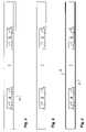
- FIG. 1shows the support membrane being used as the initial material for manufacturing a circuit-board layer, as well as an intermediate stage according to one embodiment, in which a local layer of adhesive has been added on top of the support membrane of the figure.
- FIG. 2shows an intermediate stage according to one embodiment, in which components are attached on top of the support membrane of FIG. 1 , and an insulator layer is made.
- FIG. 3shows an intermediate stage according to one embodiment, after the operations shown in FIG. 2 .
- the figurealso shows one possible intermediate product.
- FIG. 4shows the piece of FIG. 3 , after the removal of the support membrane.
- the figurealso shows a second possible intermediate product.
- FIG. 5shows the piece of FIG. 4 , after manufacture of the seed layer.
- FIG. 6shows the piece of FIG. 5 , after a patterned resist layer has been made on the surface of the piece.
- FIG. 7shows the piece of FIG. 6 , after conductor patterns have been made in the openings in the resist layer.
- FIG. 8shows the piece of FIG. 7 , after removal of the resist and the seed layer.
- FIG. 9shows one possible end product.
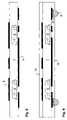
- FIG. 10shows a process diagram, which illustrates some possible embodiments of the invention.
- FIG. 11shows the division of manufacture between production plants and production lines, as well as alternatively concentration in a single production line.
- manufacturestarts from a support membrane 12 , which can be, for example, a bare metal layer ( FIG. 1 ).
- a support membrane 12can be, for example, a bare metal layer ( FIG. 1 ).
- One suitable manufacturing material for the support membrane 12is a copper film (Cu).
- the support membrane 12can also be, for example, of aluminium (Al), steel, or some insulating material, such as a polymer.
- the support membrane 12can also be a coated metal membrane, or some other membrane containing several layers, or several materials.
- Manufacturecan also be started from a support membrane 12 , on the first side of which is an insulating-material layer 1 (not shown in the figures).
- the first surfaceis the surface on the side to which the component, which is embedded inside the insulator layer 1 , is attached. Holes or recesses for the embedded components are then manufactured in the insulating-material layer 1 .
- the recessescan be made either before the insulating-material layer 1 and the support membrane 12 are attached to each other, or after they are attached. Some machining method known in the circuit-board industry, for example, milling or laser drilling can be used to make a recess. Corresponding methods can also be used to make alignment openings or other alignment markings in the support membrane 12 .
- the components 6are attached to the surface of the support membrane 12 with the aid of an adhesive ( FIG. 2 ).
- a layer of adhesive 5is spread on the attachment surface of the support membrane 12 , or the attachment surface of the component 6 , or on both attachment surfaces.
- the components 6can be aligned with the planned positions for the components 6 , for example with the aid of alignment marks.
- a support membrane 12is used, which has in itself a sufficient adhesive property that an adhesive is not required.
- the components 6are pressed directly against the support membrane 12 , in such a way that the components adhere in a corresponding manner sufficiently in place, as described in connection with the embodiment using adhesive.
- a support membrane 12can, for example, include a tape-like surfacing or consist of a polymer or corresponding material at least the surface part of which is plastic.
- the methodcan also be implemented without the use of an adhesive 5 , or an adhesive property.
- the components 6can be attached in place with the aid of a vacuum, for example.
- the vacuum or corresponding temporary attachmentcan then be maintained until the component 6 is sufficiently attached with the aid of the insulator material 1 .
- One further alternativeis to attach the components 6 with the aid of a suitable mechanical attachment.
- One embodiment using a vacuumis a vacuum table, the surface of which also acts as a support membrane 12 , or really as a support surface that replaces the support membrane 12 .
- the components 6are attached with the aid of the vacuum to the support surface, i.e. to the vacuum table and an insulating-material layer 1 is made on the surface of the table around the components 6 .
- the intermediate product formed by the insulating-material layer 1 and the components 6is lifted off the surface of the vacuum table, in other words the support surface is removed and the contact elements 7 facing towards the support surface are revealed.
- the insulator materialcan also be made, for example, by injection moulding.
- the component 6 to be attachedcan be, for example, an integrated circuit, such as a memory chip, processor, or ASIC.
- the component to be attachedcan also be, for example, a MEMS, LED, or passive component.
- the component to be attachedcan be packaged or unpackaged, and its contact elements 7 can consist of contact areas, contact bumps, or similar. On the surface of the contact areas of the component, there can also be a conductor coating that is thinner than a contact bump.
- the outer surface of the contact elements 7 of the componentwhich in the present document is referred to as the free contact surface of the contact element, can thus be on the level of the outer surface of the component, on the bottom of the recesses in the surface of the component, or on the surface of protrusions from the surface of the component.
- the contact elements 7have a first contact surface, which is in electrical contact with the semiconductor material of the component or with an internal conductor, as well as contact surface opposite to this, which is referred to as the free contact surface and which is intended for connecting an external electrical circuit to operate jointly with an internal electrical functionality of the component.
- the term attachment surface of the component 6refers to that surface of the component 6 that faces the support membrane 12 .
- the attachment surface of the component 6comprises contact elements 7 , by means of which an electrical contact can be created to the component.
- the contact elementscan be, for example, flat areas on the surface of the component 6 , contact areas, or more usually contact protrusions, such as contact bumps protruding from the surface of the component 6 .
- the component 6can comprise contact elements on other surfaces too than on the attachment surface, for example, on the opposite surface (rear surface) to the attachment surface, or on the sides between them (side surfaces).
- the term adhesiverefers to a material, by means of which the components can be attached to the support membrane.
- One property of an adhesiveis that the adhesive can be spread on the surface of the support membrane and/or the component in a liquid form, or otherwise in a form that conforms to the surface shapes, for example in the form of a membrane.
- a second property of the adhesiveis that after being spread, the adhesive hardens, or can be hardened at least partly, in such a way that the adhesive is able to hold the component in place (relative to the support membrane) for at least as long as it takes for the component to be attached to the structure in some other way.
- a third property of the adhesiveis its adhesive ability, i.e. its ability to adhere to the surface being glued.
- gluingrefers to attaching the component and the support membrane to each other with the aid of an adhesive.
- an adhesiveis brought between the component and the support membrane and the component is placed in a suitable position relative to the support membrane, in which the adhesive is in contact with the component and the support membrane and at least partly fills the space between the component and the support membrane.
- the adhesiveis allowed to harden (at least partly) or the adhesive is actively cured (at least partly), so that the component becomes attached to the support membrane with the aid of the adhesive.
- the contact elements of the componentmay protrude through the adhesive layer during gluing to come into contact with the support layer, or press partly into the support layer.
- the adhesive used in the embodimentsis, for example, a filled or unfilled thermosetting epoxy.
- the adhesiveis selected in such a way that the adhesive used has sufficient adhesion with the support layer and the component.
- One preferred property of the adhesiveis a suitable coefficient of thermal expansion, so that the thermal expansion of the adhesive will not differ too greatly from the thermal expansion of the surrounding material during the process.
- the adhesive selectedshould also preferably have a short hardening time, preferably of at most a few seconds. Within this time the adhesive should harden at least partly, in such a way that the adhesive will be able to hold the component in place. The final hardening can take clearly longer and the final hardening can, in fact, be planned to take place in connection with later process stages.
- the adhesiveshould also withstand the process temperatures used, for example, heating to a temperature of 100-265° C. a few times, as well as other stresses of the manufacturing process, for example, chemical or mechanical stress.
- the electrical conductivity of the adhesiveis preferably of the same order as the electrical conductivity of the insulating material.
- a suitable insulating-material layer 1is selected as the base material of the electronic module, for example, a circuit board.
- the insulating-material layer 1can be manufactured from a suitable polymer, or from a material containing a polymer.
- the manufacturing material of the insulating-material layer 1can be, for example, in a liquid or pre-cured form (such a prepreg).
- a glass-fibre reinforced epoxy sheetsuch as a FR4 or FR5-type sheet, for example, can be used in the manufacture of the insulating-material layer 1 .
- Other examples of materials that can be used in the manufacture of the insulating-material layer 1are PI (polyimide), aramid, polytetrafluoroethylene, and Teflon®.
- thermoplasticscan also be utilized in the manufacture of the insulating-material layer 1 , for example, some suitable LCP (liquid crystal polymer) material.
- Recesses or viasselected according to the size and mutual positions of the components 6 glued to the support membrane 12 can be made in the insulating-material layer 1 using a suitable method.
- the recesses or viascan also be manufactured to be slightly larger than the components 6 , in which case the alignment of the insulating-material layer 1 relative to the support membrane 12 will not be so critical. If the process uses an insulating-material layer 1 , in which vias are made for components 6 , certain advantages can be achieved by using in addition a separate insulating-material layer 1 , in which holes are not made (the topmost layer in FIG. 2 ).
- Such an insulating-material layer 1can be located on top of the perforated insulating-material layers 1 , to cover the vias manufactured for the components.
- the insulator-materialis cured, when an essentially unified insulating-material layer 1 ( FIG. 3 ) with be formed, both in embodiments using a single insulating-material layer 1 and in those using several insulating-material layers 1 .
- an essentially unified insulating-material layer 1FIG. 3
- an intermediate productwill have been achieved, which can be transferred to another manufacturing line for the growing of conventional circuit-board layers.
- the intermediate productcan also be packed in a delivery package for delivery to a separate factory for continuation of the circuit-board manufacture.
- a delivery package 11FIG. 11C
- Such a delivery package 11typically comprises several boards as intermediate products packed in a wrapping containing plastic and/or paper products and/or in a box, in such a way that the intermediate products can be moved for the required distance without damage.
- This transfer distancecan be, for example, to another factory in the same industrial area, or even from one country or continent to another.
- the components 6are at least substantially inside the insulator material.
- Two important examples of cases, in which the component 6 is at least substantially inside the insulator materialare the following:
- the free contact surfaces of the component 6are essentially close to the level of the outer surface of the intermediate product.
- the intermediate productcomprises a protective membrane (for example, a support membrane 12 ) that is intended to be removed and can be easily removed
- the free contact surfaces of the components 6should be essentially close to the level of the outer surface of the intermediate product, at least after the protective membrane has been removed.
- essentially closemeans that the level of the free contact surface differs from the level of the outer surface of the intermediate product generally by at most 40 micrometres and preferably by at most 20 micrometres.
- the intentis for the level of the contact surface to differ from the level of the outer surface of the intermediate product by at most 5 micrometres.
- the direction of this deviationcan be outwards or inwards from the surface of the intermediate product, i.e. in a preferred embodiment the height level of the free contact surface is between +5 . . . ⁇ 5 micrometres from the level of the surface of the intermediate product.
- the contact surfacecan be easily cleaned using a suitable method, if cleaning is necessary. This will create a readiness for making a good electrical contact.
- cleaningrefers to the removal of possible insulating material and/or impurities. Some possible cleaning methods that can be referred to are chemical cleaning, plasma cleaning, UV cleaning, and laser cleaning. Of course, other suitable methods can be used.
- a third important property of the intermediate productis that the components are accurately positioned relative to each other, at least to the extent of a single end-product module.
- end-product modulethen refers to that part of the intermediate product, which becomes one part of the electronic device that is the final product.
- the intermediate productcan thus contain several end-product modules, which in some later stage of the manufacturing process are separated from each other to form parts of an end product or end products.
- the end-product modulescan be grouped in the intermediate product into delivery blanks, which typically comprise 1-25 end-product modules.
- An entire production panelcan, in turn, comprise, for example, 1-20 delivery blanks.
- the accurate mutual alignment of the componentsis preferably also implemented inside the delivery blank, the goal being to achieve good alignment accuracy to the extent of the entire production panel too.
- the support membrane 12(and if necessary the corresponding membrane on the surface opposite to the insulator layer 1 ) is removed and the contact elements 7 of the component 6 are revealed ( FIG. 4 ).
- This stagecan also be performed before taking the intermediate product, in which case no substantial amount of the material of the support membrane 12 will remain in the intermediate product and the contact elements 7 are thus preferably revealed, so that an electrical contact can be formed to them by growing conductor material on the surface or adding it to the surface.
- the methodcan also be performed on a single manufacturing line, in which case the intermediate product is not taken from the line to be delivered to another manufacturing line.
- the holes required for viascan be manufactured in the blank.
- An electrical connection between the conductor structures on the opposite sides of the insulator layer 1can be formed later through such vias.
- the making of the holescan take place before or after the aforementioned intermediate-product stages.
- a conductor-pattern layer 4can be made on the surface of the insulator layer 1 , so that it forms electrical contacts with selected contact elements 7 .
- a conductor-pattern layercan also be manufactured on the opposite surface of the insulator layer.
- the manufacture of the conductor-pattern layercan be performed in several different ways.
- the conductor layeris manufactured by using a growing method to grow on top of a conductor membrane. In that case, the conductor membrane is grown directly in its correct shape
- the conductor-pattern layeris manufactured using a printing method, for example, from a conductive paste.
- a unified conductor layeris made on the surfaces of the intermediate product, from which in turn conductor patterns are made by removing areas of the material of the conductor layer. The areas can be removed, for example, using a photolithography method, or a laser-ablation method.
- the conductor-pattern layeris manufactured by outputting or printing, utilizing a conductive ink (e.g., metal ink), which typically contains conductive metal and/or carbon particles.
- a conductive inke.g., metal ink
- the conductor-pattern layeris manufactured by outputting or printing, utilizing a conductive polymer.
- the outputting technique usedcan be, for example, a suitable selective dosing technique, such as the inkjet technique, or the additive writing technique.
- the conductor-pattern layercan also be manufactured using some other method that traces or produces electrical conductors.
- the surface or surfaces of the insulator layer 1can be treated, in order to improve the adhesion of the conductor layer.
- the treatmentcan be performed, for example, between the stages shown in FIGS. 4 and 5 , by treating the surface of the insulator layer 1 in such a way as to improve the adhesion of the seed metal of the conductor layer on the surface of the insulator layer 1 . Thanks to the improved adhesion, narrower conductor structures can be made in the module, and a denser network of conductors achieved.
- the surface treatmentcan be performed, for example, chemically, by plasma, with the aid of UV radiation, or by laser.
- the procedureis thus to grow a thin seed layer 2 of metal ( FIG. 5 ) on both surfaces of the insulating-material layer 1 .
- the seed layer 2can be, for example, of chemically grown copper. If holes have been made in the insulating-material layer 1 for vias, the seed layer 2 will also grow on the inner surfaces of the holes.
- manufactureis continued by spreading resist layers 3 , typically photo-resist layers, on the surfaces of the seed layers 2 .
- resist layers 3typically photo-resist layers
- the resist layers 3are exposed through a patterned mask and after this the blank is developed. After developing, the exposed resist layers 3 will be patterned as desired to form conductor-pattern masks ( FIG. 6 ). A corresponding result can also be achieved using alternative lithography techniques.
- manufactureis continued by growing a conductor material, typically copper, electrolytically in the areas from which the photo resist 3 was removed.
- the desired conductor patterns 4( FIG. 7 ) are then formed on the surfaces of the seed layers 2 .
- the thickness of the conductor pattern 4can be, for example, 20 micrometers while the line width of the conductor patterns being manufactured can also be less than 20 micrometers.
- the methodcan also be used to make small and precise conductor patterns.
- the methodcan be modified in such a way that a layer of a second metal or metal allow, for example tin, is manufactured on the surface of the conductor patterns 4 or on the interface between the seed layers 2 and the conductor patterns 4 .
- This layercan be used as an etching stopper.
- the resist layers 3can be removed.
- the seed layers 2are removed, for example, by etching ( FIG. 8 ).
- the circuit-board productmay already be finished, but more usually manufacture is continued by making additional alternating insulator layer and conductor-pattern layers on the surfaces of the circuit board, as well as vias, which connect the conductor-pattern layers to each other.
- manufactureis continued by making insulator layers 10 on the surfaces of the blank shown in FIG. 8 , as well as the external contact elements of the module.
- the external contact elementsinclude bases 8 made on top of the conductor patterns, as well as contact balls 9 made on their surfaces.
- FIG. 10The method described above and possible variations of it are also illustrated in FIG. 10 .
- FIG. 10According to FIG. 10 :
- a componentis attached to the support membrane. This can be performed using the manner described above with the aid of an adhesive, or without an adhesive by using a support membrane possessing a suitable adhesive capability.
- the insulator layeris manufactured. This can be performed, for example, as described above.
- stage 103a suitable method is used to remove the support membrane.
- the removalcan take place, for example, mechanically or chemically or by combining a mechanical and a chemical method. If necessary, an additional stage of the method is performed in order to open the contact elements of the component.
- stage 104the conductor patterns are made and an electrical contact is formed to the attachment elements of the components.
- the manufacture of the conductor patterncan be performed, for example, using methods described above, or by some other suitable conductor-pattern manufacturing method. If necessary, at the start of the stage an additional stage of the method is performed to open the contact elements of the component, or to clean the surface of the contact elements.
- circuit boardIn the optional stage 105 , further processing of the circuit board takes place, for example, the manufacture of additional layers, the manufacture and/or protection of the contact parts.
- FIGS. 11A , 11 B, and 11 Cillustrate the idea of dividing the manufacturing lines.
- FIG. 11Ashows an alternative, in which the manufacturing method is implemented entirely in a single production plant and with the aid of a unified manufacturing line.
- the intermediate productdoes not actually have to be taken from the process, but instead manufacture continues up until an essentially finished circuit board or electronic module.
- This solutionis very suitable, for example, for a situation in which it is desired to construct and entirely hew production plant or production line, for the manufacture of highly developed electronic modules.
- FIG. 11Bshows a situation, in which two separate manufacturing lines are used in the same production plant. On the first line, method stages 101 - 102 , or 101 - 103 are performed, while on the second line the process continues correspondingly with stage 103 or 104 .
- This form of implementationcan very well be considered, for example, in a case in which there is an existing circuit-board manufacturing line with sufficient performance in the production plant and it is wished to expand the production capacity of the production plant to highly developed electronic modules, which contain embedded active components. In that case, a new manufacturing line can be built in the production plant, by means of which intermediate products A or B (stages 101 - 102 , or 101 - 103 ) are manufactured and then transferred to a circuit-board manufacturing line for further processing. In this case, there is often no need to package the intermediate products in a delivery package.
- FIG. 11Cshows a situation, in which the method stages are divided to be performed in two separate production plants.
- the intermediate products A or B(stages 101 - 102 , or 101 - 103 ) are manufactured and transferred to the second production plant for further processing.
- This form of implementationis competitive, for example, when it is wished to produce highly developed electronic modules in a production plant with a high-performance circuit-board manufacturing line, without additional investments for a component assembly line.
- the intermediate products A or Bcan be ordered from another production plant, which manufactures intermediate products and in which they are packed in a delivery package 11 for transporting the intermediate products. In this way, in even a production plant with a high-performance circuit-board manufacturing line, it is possible to manufacture, for example, the products described in publication WO 2004/089048.
- the contact elements 7 of the component 6protrude outwards from the level of the surface of the component.
- components 6in which the free contact surfaces of the contact elements 7 are essentially on the level of the corresponding surface of the component, i.e. of the attachment surface.
- the component 6is also preferably pressed against the support membrane 12 .
- the pressingpreferably takes place in such a way that practically no adhesive remains between the component 6 and the support membrane 12 .
- the component 6is of course naturally pressed against the support membrane 12 .
- Components 6 , the passivation and protection layer of the surface of which is sufficient to permit a conductor pattern to be made directly on the surface of such a passivation and protection layer,are particularly well suited to such a method.
- insulator membraneof a thickness of, for example, 1-20 micrometres.
- the attachment of the conductor material, for example copper, in the vicinity of the componentcan be improved, because the adhesion of the conductor material is not necessarily good on the actual surface of the component, which is, for example, of silicon.
- the insulator membranecan also help to control the deformations that arise between the component and the conductor pattern due to the effect of, for example, temperature variations.
Landscapes
- Engineering & Computer Science (AREA)
- Microelectronics & Electronic Packaging (AREA)
- Computer Hardware Design (AREA)
- Power Engineering (AREA)
- Mechanical Engineering (AREA)
- Manufacturing & Machinery (AREA)
- General Engineering & Computer Science (AREA)
- Chemical & Material Sciences (AREA)
- Combustion & Propulsion (AREA)
- Physics & Mathematics (AREA)
- Condensed Matter Physics & Semiconductors (AREA)
- General Physics & Mathematics (AREA)
- Manufacturing Of Printed Wiring (AREA)
- Production Of Multi-Layered Print Wiring Board (AREA)
Abstract
Description
- 1. Field of the Invention
- The present invention relates to a method for manufacturing a circuit board containing a component, as well as to a circuit board containing a component.
- 2. Brief Description of the Related Art
- Layers containing a component are manufactured, for example, when manufacturing multi-layer circuit boards or other corresponding electronic modules. In particular, the invention relates to a method for manufacturing a layer, which contains one or several components, which are connected electrically to an external circuit, or to each other, with the aid of conductor structures manufactured in the electronic module.
- US Publication No. 2005/0001331 discloses a manufacturing method for circuit-board structure, in which first of all a circuit board, which comprises an insulator layer and a conductor pattern on the surface of it, is manufactured. After that, a semiconductor component is then connected to the conductor pattern of the surface of the circuit board, using a suitable flip-chip attachment method. The connection is made with the aid of contact bumps on the surface of the semiconductor component. In the method of the US publication, after attachment of the component, a patterned and unpatterned insulating-material layer is laminated on top of the circuit board and then on their surface a conductor-pattern layer.
- U.S. Pat. No. 6,038,133 and U.S. Pat. No. 6,489,685, as well as US Publication No. 2002/0117743 disclose methods, in which a conductor pattern is made on the surface of a detachable membrane and a semiconductor component is attached to the conductor pattern using a flip-chip attachment method. After this, the component is surrounded with a layer of insulating material and the detachable membrane is removed.
- The aforementioned U.S. Pat. No. 6,038,133 and US Publication No. 2002/0117743 also disclose a method, in which a flip-chip method is used to attach the component not to a conductor pattern, but to a unified conductor membrane, from which conductor patterns are formed in a later stage of the process. A corresponding method is also disclosed in, for example, U.S. Pat. No. 5,042,145, WO 2004/077902, WO 2004/077903, and WO 2005/020651.
- In addition to the types of method referred to above, many other methods are known, by means of which circuit-board structures containing components can be manufactured. For example, the components can be first of all placed inside an insulating-material layer and connected electrically to the conductor layer only after this, as is disclosed in International Publication No. WO 2004/089048. In the method of WO 2004/089048, the component is glued onto the surface of the conductor layer and after the component has been glued an insulating-material layer is formed on, or attached to the surface of the conductor layer. After the gluing of the component, vias are also made, through which electrical contacts can be formed between the conductor layer and the component. After this, conductor patterns are formed from the conductor layer, to the surface of which the component has been glued. With the aid of the method described by the publication, it is possible to manufacture mechanically durable electronic modules, which contain embedded unpacked components. A good side of the method is also the fact that the contacts to the components can be made by growing metal, in which case the electrical properties of the contacts will be excellent.
- However, the method disclosed in WO 2004/089048 differs from the conventional circuit-board manufacturing process to such an extent that its introduction to mass production will in most cases require the construction of a new manufacturing line, or at least alterations to a traditional manufacturing line. Thus the introduction of the method will also demand considerable initial investments.
- The invention is intended to improve the method disclosed in WO 2004/089048, so that it can be exploited more easily also in connection with traditional circuit-board manufacturing processes.
- The invention is based on first of all manufacturing an intermediate product, which contains the insulator layer of the circuit board and the components, which are attached in place inside the insulator layer, in such a way that the contact elements of the components open onto the surface of the intermediate product, or at least extend into the vicinity of the surface of the intermediate product. After this, the intermediate product is transferred to a circuit-board manufacturing line, on which a suitable number of conductor-pattern layers, and if necessary insulator layers are made on one or both sides of the intermediate product, in such a way that in the manufacture of the first conductor-pattern layer the conductor material forms an electrical contact with the contact elements of the components.
- At the same time, according to the invention an alternative method is also created for manufacturing the product described in WO 2004/089048.
- Considerable advantages are gained with the aid of the invention.
- With the aid according to the invention, the method disclosed in WO 2004/089048 can be more easily utilized also in connection with traditional circuit-board manufacturing processes.
- With the aid of the invention, an alternative method is also presented for manufacturing the product described in WO 2004/089048.
- Further scope of the applicability of the present invention will become apparent from the detailed description given hereinafter. However, it should be understood that the detailed description and specific examples, while indicating preferred embodiments of the invention, are given by way of illustration only, since various changes and modifications within the spirit and scope of the invention will become apparent to those skilled in the art from this detailed description.
- The present invention will become more fully understood from the detailed description given hereinbelow and the accompanying drawings, which are given by way of illustration only, and thus are not limitative of the present invention.
FIG. 1 shows the support membrane being used as the initial material for manufacturing a circuit-board layer, as well as an intermediate stage according to one embodiment, in which a local layer of adhesive has been added on top of the support membrane of the figure.FIG. 2 shows an intermediate stage according to one embodiment, in which components are attached on top of the support membrane ofFIG. 1 , and an insulator layer is made.FIG. 3 shows an intermediate stage according to one embodiment, after the operations shown inFIG. 2 . The figure also shows one possible intermediate product.FIG. 4 shows the piece ofFIG. 3 , after the removal of the support membrane. The figure also shows a second possible intermediate product.FIG. 5 shows the piece ofFIG. 4 , after manufacture of the seed layer.FIG. 6 shows the piece ofFIG. 5 , after a patterned resist layer has been made on the surface of the piece.FIG. 7 shows the piece ofFIG. 6 , after conductor patterns have been made in the openings in the resist layer.FIG. 8 shows the piece ofFIG. 7 , after removal of the resist and the seed layer.FIG. 9 shows one possible end product.FIG. 10 shows a process diagram, which illustrates some possible embodiments of the invention.FIG. 11 shows the division of manufacture between production plants and production lines, as well as alternatively concentration in a single production line.- In the methods according to the embodiments, manufacture starts from a
support membrane 12, which can be, for example, a bare metal layer (FIG. 1 ). One suitable manufacturing material for thesupport membrane 12 is a copper film (Cu). Thesupport membrane 12 can also be, for example, of aluminium (Al), steel, or some insulating material, such as a polymer. Thesupport membrane 12 can also be a coated metal membrane, or some other membrane containing several layers, or several materials. - Manufacture can also be started from a
support membrane 12, on the first side of which is an insulating-material layer1 (not shown in the figures). In that case, the first surface is the surface on the side to which the component, which is embedded inside theinsulator layer 1, is attached. Holes or recesses for the embedded components are then manufactured in the insulating-material layer 1. The recesses can be made either before the insulating-material layer 1 and thesupport membrane 12 are attached to each other, or after they are attached. Some machining method known in the circuit-board industry, for example, milling or laser drilling can be used to make a recess. Corresponding methods can also be used to make alignment openings or other alignment markings in thesupport membrane 12. - In the embodiments shown in the figures, the
components 6 are attached to the surface of thesupport membrane 12 with the aid of an adhesive (FIG. 2 ). For gluing, a layer ofadhesive 5 is spread on the attachment surface of thesupport membrane 12, or the attachment surface of thecomponent 6, or on both attachment surfaces. After this, thecomponents 6 can be aligned with the planned positions for thecomponents 6, for example with the aid of alignment marks. - In an alternative embodiment, a
support membrane 12 is used, which has in itself a sufficient adhesive property that an adhesive is not required. In that case, thecomponents 6 are pressed directly against thesupport membrane 12, in such a way that the components adhere in a corresponding manner sufficiently in place, as described in connection with the embodiment using adhesive. Such asupport membrane 12 can, for example, include a tape-like surfacing or consist of a polymer or corresponding material at least the surface part of which is plastic. - The method can also be implemented without the use of an adhesive5, or an adhesive property. In that case, the
components 6 can be attached in place with the aid of a vacuum, for example. The vacuum or corresponding temporary attachment can then be maintained until thecomponent 6 is sufficiently attached with the aid of theinsulator material 1. One further alternative is to attach thecomponents 6 with the aid of a suitable mechanical attachment. - One embodiment using a vacuum is a vacuum table, the surface of which also acts as a
support membrane 12, or really as a support surface that replaces thesupport membrane 12. In that case, thecomponents 6 are attached with the aid of the vacuum to the support surface, i.e. to the vacuum table and an insulating-material layer 1 is made on the surface of the table around thecomponents 6. After this, the intermediate product formed by the insulating-material layer 1 and thecomponents 6 is lifted off the surface of the vacuum table, in other words the support surface is removed and thecontact elements 7 facing towards the support surface are revealed. When using a support surface, the insulator material can also be made, for example, by injection moulding. - The
component 6 to be attached can be, for example, an integrated circuit, such as a memory chip, processor, or ASIC. The component to be attached can also be, for example, a MEMS, LED, or passive component. The component to be attached can be packaged or unpackaged, and itscontact elements 7 can consist of contact areas, contact bumps, or similar. On the surface of the contact areas of the component, there can also be a conductor coating that is thinner than a contact bump. The outer surface of thecontact elements 7 of the component, which in the present document is referred to as the free contact surface of the contact element, can thus be on the level of the outer surface of the component, on the bottom of the recesses in the surface of the component, or on the surface of protrusions from the surface of the component. For reasons of clarity, it should be further stated that thecontact elements 7 have a first contact surface, which is in electrical contact with the semiconductor material of the component or with an internal conductor, as well as contact surface opposite to this, which is referred to as the free contact surface and which is intended for connecting an external electrical circuit to operate jointly with an internal electrical functionality of the component. - The term attachment surface of the
component 6 refers to that surface of thecomponent 6 that faces thesupport membrane 12. The attachment surface of thecomponent 6 comprisescontact elements 7, by means of which an electrical contact can be created to the component. The contact elements can be, for example, flat areas on the surface of thecomponent 6, contact areas, or more usually contact protrusions, such as contact bumps protruding from the surface of thecomponent 6. There are generally at least two contact elements in thecomponent 6. In complex microcircuits, there can be very many contact elements. Thecomponent 6 can comprise contact elements on other surfaces too than on the attachment surface, for example, on the opposite surface (rear surface) to the attachment surface, or on the sides between them (side surfaces). - It is generally preferably to spread so much adhesive on the attachment surface or attachment surfaces that the adhesive entirely fills the space remaining between the
components 6 and thesupport membrane 12. The unified adhesive layer will then protect the component in the direction of the attachment surface. - The term adhesive refers to a material, by means of which the components can be attached to the support membrane. One property of an adhesive is that the adhesive can be spread on the surface of the support membrane and/or the component in a liquid form, or otherwise in a form that conforms to the surface shapes, for example in the form of a membrane. A second property of the adhesive is that after being spread, the adhesive hardens, or can be hardened at least partly, in such a way that the adhesive is able to hold the component in place (relative to the support membrane) for at least as long as it takes for the component to be attached to the structure in some other way. A third property of the adhesive is its adhesive ability, i.e. its ability to adhere to the surface being glued.
- The term gluing refers to attaching the component and the support membrane to each other with the aid of an adhesive. Thus in gluing an adhesive is brought between the component and the support membrane and the component is placed in a suitable position relative to the support membrane, in which the adhesive is in contact with the component and the support membrane and at least partly fills the space between the component and the support membrane. After this, the adhesive is allowed to harden (at least partly) or the adhesive is actively cured (at least partly), so that the component becomes attached to the support membrane with the aid of the adhesive. In some embodiments, the contact elements of the component may protrude through the adhesive layer during gluing to come into contact with the support layer, or press partly into the support layer.
- The adhesive used in the embodiments is, for example, a filled or unfilled thermosetting epoxy. The adhesive is selected in such a way that the adhesive used has sufficient adhesion with the support layer and the component. One preferred property of the adhesive is a suitable coefficient of thermal expansion, so that the thermal expansion of the adhesive will not differ too greatly from the thermal expansion of the surrounding material during the process. The adhesive selected should also preferably have a short hardening time, preferably of at most a few seconds. Within this time the adhesive should harden at least partly, in such a way that the adhesive will be able to hold the component in place. The final hardening can take clearly longer and the final hardening can, in fact, be planned to take place in connection with later process stages. The adhesive should also withstand the process temperatures used, for example, heating to a temperature of 100-265° C. a few times, as well as other stresses of the manufacturing process, for example, chemical or mechanical stress. The electrical conductivity of the adhesive is preferably of the same order as the electrical conductivity of the insulating material.
- A suitable insulating-
material layer 1 is selected as the base material of the electronic module, for example, a circuit board. The insulating-material layer 1 can be manufactured from a suitable polymer, or from a material containing a polymer. The manufacturing material of the insulating-material layer 1 can be, for example, in a liquid or pre-cured form (such a prepreg). A glass-fibre reinforced epoxy sheet, such as a FR4 or FR5-type sheet, for example, can be used in the manufacture of the insulating-material layer 1. Other examples of materials that can be used in the manufacture of the insulating-material layer 1 are PI (polyimide), aramid, polytetrafluoroethylene, and Teflon®. Instead of, or along with thermosetting plastics, thermoplastics can also be utilized in the manufacture of the insulating-material layer 1, for example, some suitable LCP (liquid crystal polymer) material. - Recesses or vias (
FIG. 2 ) selected according to the size and mutual positions of thecomponents 6 glued to thesupport membrane 12 can be made in the insulating-material layer 1 using a suitable method. The recesses or vias can also be manufactured to be slightly larger than thecomponents 6, in which case the alignment of the insulating-material layer 1 relative to thesupport membrane 12 will not be so critical. If the process uses an insulating-material layer 1, in which vias are made forcomponents 6, certain advantages can be achieved by using in addition a separate insulating-material layer 1, in which holes are not made (the topmost layer inFIG. 2 ). Such an insulating-material layer 1 can be located on top of the perforated insulating-material layers 1, to cover the vias manufactured for the components. - After this the insulator-material is cured, when an essentially unified insulating-material layer1 (
FIG. 3 ) with be formed, both in embodiments using a single insulating-material layer 1 and in those using several insulating-material layers1. At the same time it is possible to laminate a membrane corresponding to thesupport membrane 12, also on the other surface of theinsulator layer 1, in which case the intermediate product obtained will be in equilibrium in terms of mechanical stresses. - At this stage in the method, an intermediate product will have been achieved, which can be transferred to another manufacturing line for the growing of conventional circuit-board layers. The intermediate product can also be packed in a delivery package for delivery to a separate factory for continuation of the circuit-board manufacture. Such a delivery package11 (
FIG. 11C ) typically comprises several boards as intermediate products packed in a wrapping containing plastic and/or paper products and/or in a box, in such a way that the intermediate products can be moved for the required distance without damage. This transfer distance can be, for example, to another factory in the same industrial area, or even from one country or continent to another. - One important property of the intermediate product is that the
components 6 are at least substantially inside the insulator material. Two important examples of cases, in which thecomponent 6 is at least substantially inside the insulator material are the following: - The
component 6 is entirely inside the insulator material. In that case, there is insulator material on the attachment surface, rear surface, and side surfaces of thecomponent 6. - The
component 6 is surrounded by the insulator material. In that case, there is insulator material on the side surfaces of thecomponent 6, but the attachment surface of the component is essentially free of insulator material. Also the rear surface of the component is typically covered with insulator material, but it is also possible for the rear surface of the component to be essentially free of insulator material.
- The
- Another important property of the intermediate product is that the free contact surfaces of the
component 6 are essentially close to the level of the outer surface of the intermediate product. If the intermediate product comprises a protective membrane (for example, a support membrane12) that is intended to be removed and can be easily removed, the free contact surfaces of thecomponents 6 should be essentially close to the level of the outer surface of the intermediate product, at least after the protective membrane has been removed. In this connection, essentially close means that the level of the free contact surface differs from the level of the outer surface of the intermediate product generally by at most 40 micrometres and preferably by at most 20 micrometres. In more demanding applications, the intent is for the level of the contact surface to differ from the level of the outer surface of the intermediate product by at most 5 micrometres. The direction of this deviation can be outwards or inwards from the surface of the intermediate product, i.e. in a preferred embodiment the height level of the free contact surface is between +5 . . . −5 micrometres from the level of the surface of the intermediate product. - If the component, or at least its free contact surface is close to the level of the surface of the intermediate product, the contact surface can be easily cleaned using a suitable method, if cleaning is necessary. This will create a readiness for making a good electrical contact. The term cleaning refers to the removal of possible insulating material and/or impurities. Some possible cleaning methods that can be referred to are chemical cleaning, plasma cleaning, UV cleaning, and laser cleaning. Of course, other suitable methods can be used.
- A third important property of the intermediate product is that the components are accurately positioned relative to each other, at least to the extent of a single end-product module. The term end-product module then refers to that part of the intermediate product, which becomes one part of the electronic device that is the final product.
- The intermediate product can thus contain several end-product modules, which in some later stage of the manufacturing process are separated from each other to form parts of an end product or end products. The end-product modules can be grouped in the intermediate product into delivery blanks, which typically comprise 1-25 end-product modules. An entire production panel can, in turn, comprise, for example, 1-20 delivery blanks. The accurate mutual alignment of the components is preferably also implemented inside the delivery blank, the goal being to achieve good alignment accuracy to the extent of the entire production panel too.
- When the circuit-board manufacture continues, the support membrane12 (and if necessary the corresponding membrane on the surface opposite to the insulator layer1) is removed and the
contact elements 7 of thecomponent 6 are revealed (FIG. 4 ). This stage can also be performed before taking the intermediate product, in which case no substantial amount of the material of thesupport membrane 12 will remain in the intermediate product and thecontact elements 7 are thus preferably revealed, so that an electrical contact can be formed to them by growing conductor material on the surface or adding it to the surface. In addition, it should be noted that the method can also be performed on a single manufacturing line, in which case the intermediate product is not taken from the line to be delivered to another manufacturing line. - After the insulating-material layer has hardened sufficiently, the holes required for vias (not shown in the figures) can be manufactured in the blank. An electrical connection between the conductor structures on the opposite sides of the
insulator layer 1 can be formed later through such vias. The making of the holes can take place before or after the aforementioned intermediate-product stages. - Irrespective of the stage at which the intermediate product is taken (or whether manufacture is continued directly on the same line), a conductor-
pattern layer 4 can be made on the surface of theinsulator layer 1, so that it forms electrical contacts with selectedcontact elements 7. In a corresponding manner and at a corresponding stage a conductor-pattern layer can also be manufactured on the opposite surface of the insulator layer. - The manufacture of the conductor-pattern layer can be performed in several different ways. According to one embodiment, the conductor layer is manufactured by using a growing method to grow on top of a conductor membrane. In that case, the conductor membrane is grown directly in its correct shape According to a second embodiment, the conductor-pattern layer is manufactured using a printing method, for example, from a conductive paste. According to a third embodiment, a unified conductor layer is made on the surfaces of the intermediate product, from which in turn conductor patterns are made by removing areas of the material of the conductor layer. The areas can be removed, for example, using a photolithography method, or a laser-ablation method. In a fourth embodiment, the conductor-pattern layer is manufactured by outputting or printing, utilizing a conductive ink (e.g., metal ink), which typically contains conductive metal and/or carbon particles. In a fifth embodiment, the conductor-pattern layer is manufactured by outputting or printing, utilizing a conductive polymer. The outputting technique used can be, for example, a suitable selective dosing technique, such as the inkjet technique, or the additive writing technique. The conductor-pattern layer can also be manufactured using some other method that traces or produces electrical conductors.
- Before the manufacture of the conductor pattern, the surface or surfaces of the
insulator layer 1 can be treated, in order to improve the adhesion of the conductor layer. The treatment can be performed, for example, between the stages shown inFIGS. 4 and 5 , by treating the surface of theinsulator layer 1 in such a way as to improve the adhesion of the seed metal of the conductor layer on the surface of theinsulator layer 1. Thanks to the improved adhesion, narrower conductor structures can be made in the module, and a denser network of conductors achieved. The surface treatment can be performed, for example, chemically, by plasma, with the aid of UV radiation, or by laser. - In general, it is not, however, necessary to manufacture a conductor pattern on the surface of the intermediate product shown in
FIG. 4 , but instead it is possible to continue from this stage using any method whatever, with the aid of which it is possible to create the necessary electrical contacts to thecomponents 6. One alternative is to attach another intermediate product to the surface of the intermediate product, when the intermediate products are aligned relative to each other and pressed and attached against each other. In that case, contact structures, with the aid of which a good electrical contact can be ensured, can if necessary be prefabricated on the free contact surfaces of the components contained in either or both of the intermediate products. It is also possible to press only a prefabricated conductor structure against the surface of the intermediate product. It is also possible to continue from the intermediate product with the aid of wire bonding, or some other known method. - In the embodiment shown in the figures, the procedure is thus to grow a
thin seed layer 2 of metal (FIG. 5 ) on both surfaces of the insulating-material layer 1. Theseed layer 2 can be, for example, of chemically grown copper. If holes have been made in the insulating-material layer 1 for vias, theseed layer 2 will also grow on the inner surfaces of the holes. After this, manufacture is continued by spreading resistlayers 3, typically photo-resist layers, on the surfaces of the seed layers2. In more precise embodiments, it is also possible to use a lithography technique based on the use of electromagnetic radiation of shorter wavelength, or for example an electron beam lithography technique. In the case of a photo resist, the resistlayers 3 are exposed through a patterned mask and after this the blank is developed. After developing, the exposed resistlayers 3 will be patterned as desired to form conductor-pattern masks (FIG. 6 ). A corresponding result can also be achieved using alternative lithography techniques. - In the example of the figure, manufacture is continued by growing a conductor material, typically copper, electrolytically in the areas from which the photo resist3 was removed. The desired conductor patterns4 (
FIG. 7 ) are then formed on the surfaces of the seed layers2. The thickness of theconductor pattern 4 can be, for example, 20 micrometers while the line width of the conductor patterns being manufactured can also be less than 20 micrometers. Thus the method can also be used to make small and precise conductor patterns. - The method can be modified in such a way that a layer of a second metal or metal allow, for example tin, is manufactured on the surface of the
conductor patterns 4 or on the interface between the seed layers2 and theconductor patterns 4. This layer can be used as an etching stopper. - After the manufacture of the
conductor patterns 4, the resistlayers 3 can be removed. In addition the seed layers2 are removed, for example, by etching (FIG. 8 ). After this, the circuit-board product may already be finished, but more usually manufacture is continued by making additional alternating insulator layer and conductor-pattern layers on the surfaces of the circuit board, as well as vias, which connect the conductor-pattern layers to each other. - In the example of
FIG. 9 , manufacture is continued by making insulator layers10 on the surfaces of the blank shown inFIG. 8 , as well as the external contact elements of the module. The external contact elements includebases 8 made on top of the conductor patterns, as well ascontact balls 9 made on their surfaces. - The method described above and possible variations of it are also illustrated in
FIG. 10 . According toFIG. 10 : - In
stage 101, a component is attached to the support membrane. This can be performed using the manner described above with the aid of an adhesive, or without an adhesive by using a support membrane possessing a suitable adhesive capability. - In
stage 102, the insulator layer is manufactured. This can be performed, for example, as described above. - In
stage 103, a suitable method is used to remove the support membrane. The removal can take place, for example, mechanically or chemically or by combining a mechanical and a chemical method. If necessary, an additional stage of the method is performed in order to open the contact elements of the component. - In
stage 104, the conductor patterns are made and an electrical contact is formed to the attachment elements of the components. The manufacture of the conductor pattern can be performed, for example, using methods described above, or by some other suitable conductor-pattern manufacturing method. If necessary, at the start of the stage an additional stage of the method is performed to open the contact elements of the component, or to clean the surface of the contact elements. - In the
optional stage 105, further processing of the circuit board takes place, for example, the manufacture of additional layers, the manufacture and/or protection of the contact parts. - As can be seen from
FIG. 19 , it is most suitable to take the intermediate product betweenstages 102 and103 (intermediate product A), or betweenstages 103 and104 (intermediate product B). Processing is then correspondingly continued on another manufacturing line, or in another factory from stage103 (intermediate product A) or from stage104 (intermediate product B). FIGS. 11A ,11B, and11C illustrate the idea of dividing the manufacturing lines.FIG. 11A shows an alternative, in which the manufacturing method is implemented entirely in a single production plant and with the aid of a unified manufacturing line. In that case, the intermediate product does not actually have to be taken from the process, but instead manufacture continues up until an essentially finished circuit board or electronic module. This solution is very suitable, for example, for a situation in which it is desired to construct and entirely hew production plant or production line, for the manufacture of highly developed electronic modules.FIG. 11B shows a situation, in which two separate manufacturing lines are used in the same production plant. On the first line, method stages101-102, or101-103 are performed, while on the second line the process continues correspondingly withstage FIG. 11C shows a situation, in which the method stages are divided to be performed in two separate production plants. In the first production plant, the intermediate products A or B (stages101-102, or101-103) are manufactured and transferred to the second production plant for further processing. This form of implementation is competitive, for example, when it is wished to produce highly developed electronic modules in a production plant with a high-performance circuit-board manufacturing line, without additional investments for a component assembly line. In that case, the intermediate products A or B can be ordered from another production plant, which manufactures intermediate products and in which they are packed in adelivery package 11 for transporting the intermediate products. In this way, in even a production plant with a high-performance circuit-board manufacturing line, it is possible to manufacture, for example, the products described in publication WO 2004/089048.- In the embodiment shown in the figures, the
contact elements 7 of thecomponent 6 protrude outwards from the level of the surface of the component. As will have already become apparent from the preceding description, it is, however, also possible in the method to usecomponents 6, in which the free contact surfaces of thecontact elements 7 are essentially on the level of the corresponding surface of the component, i.e. of the attachment surface. In that case, thecomponent 6 is also preferably pressed against thesupport membrane 12. When using an adhesive5 and relativelyhard support membrane 12, the pressing preferably takes place in such a way that practically no adhesive remains between thecomponent 6 and thesupport membrane 12. In an attachment implemented without an adhesive, thecomponent 6 is of course naturally pressed against thesupport membrane 12.Components 6, the passivation and protection layer of the surface of which is sufficient to permit a conductor pattern to be made directly on the surface of such a passivation and protection layer, are particularly well suited to such a method. - The examples presented above describe some possible processes, with the aid of which our invention can be exploited. However, our invention is not restricted to only the first and second embodiment described above, but instead the invention encompasses other different processes and their end products too, in the full scope of the Claims and taking equivalence interpretation into account. The invention is also not restricted to only the constructions and methods depicted in the examples, but instead it will be obvious to one skilled in the art that various applications of the invention can be used to manufacture very many different kind of electronic module and circuit board, which differ even greatly from the examples presented above. The components and circuits of the figures are thus shown only with the intention to illustrate the manufacturing process. Thus very many alterations can be made to the processes of the examples shown above, while nevertheless not deviating from the basic idea according to the invention. The alterations can relate, for example, to the manufacturing techniques described in the various stages, or to the mutual sequence of the process stages.
- One possible variation that can be mentioned is that it is possible to add to the support membrane12 a thin insulator membrane, of a thickness of, for example, 1-20 micrometres. With the aid of such an insulator membrane, the attachment of the conductor material, for example copper, in the vicinity of the component can be improved, because the adhesion of the conductor material is not necessarily good on the actual surface of the component, which is, for example, of silicon. The insulator membrane can also help to control the deformations that arise between the component and the conductor pattern due to the effect of, for example, temperature variations.
- The invention being thus described, it will be obvious that the same may be varied in many ways. Such variations are not to be regarded as a departure from the spirit and scope of the invention, and all such modifications as would be obvious to one skilled in the art are intended to be included within the scope of the following claims.
Claims (12)
Applications Claiming Priority (5)
| Application Number | Priority Date | Filing Date | Title |
|---|---|---|---|
| BRP10502146-4 | 2005-06-06 | ||
| BRP10600645.0 | 2006-02-15 | ||
| FI20060256 | 2006-03-17 | ||
| FI20060256AFI20060256A7 (en) | 2006-03-17 | 2006-03-17 | Circuit board manufacturing and circuit board containing the component |
| PCT/FI2007/050141WO2007107630A1 (en) | 2006-03-17 | 2007-03-15 | Manufacture of a circuit board and circuit board containing a component |
Related Parent Applications (1)
| Application Number | Title | Priority Date | Filing Date |
|---|---|---|---|
| PCT/FI2007/050141A-371-Of-InternationalWO2007107630A1 (en) | 2006-03-17 | 2007-03-15 | Manufacture of a circuit board and circuit board containing a component |
Related Child Applications (1)
| Application Number | Title | Priority Date | Filing Date |
|---|---|---|---|
| US14/660,991ContinuationUS10085347B2 (en) | 2006-03-17 | 2015-03-18 | Manufacture of a circuit board and circuit board containing a component |
Publications (2)
| Publication Number | Publication Date |
|---|---|
| US20090133251A1true US20090133251A1 (en) | 2009-05-28 |
| US8984746B2 US8984746B2 (en) | 2015-03-24 |
Family
ID=36191882
Family Applications (2)
| Application Number | Title | Priority Date | Filing Date |
|---|---|---|---|
| US12/293,412Active2030-11-07US8984746B2 (en) | 2006-03-17 | 2007-03-15 | Manufacture of a circuit board containing a component |
| US14/660,991Active2028-09-02US10085347B2 (en) | 2006-03-17 | 2015-03-18 | Manufacture of a circuit board and circuit board containing a component |
Family Applications After (1)
| Application Number | Title | Priority Date | Filing Date |
|---|---|---|---|
| US14/660,991Active2028-09-02US10085347B2 (en) | 2006-03-17 | 2015-03-18 | Manufacture of a circuit board and circuit board containing a component |
Country Status (7)
| Country | Link |
|---|---|
| US (2) | US8984746B2 (en) |
| EP (1) | EP1997360A1 (en) |
| JP (1) | JP2009530801A (en) |
| KR (1) | KR20080106977A (en) |
| CN (1) | CN101449632A (en) |
| FI (1) | FI20060256A7 (en) |
| WO (1) | WO2007107630A1 (en) |
Cited By (16)
| Publication number | Priority date | Publication date | Assignee | Title |
|---|---|---|---|---|
| US20090242255A1 (en)* | 2008-03-27 | 2009-10-01 | Ibiden Co., Ltd | Wiring board with built-in electronic component and method of manufacturing same |
| US20100133666A1 (en)* | 2008-12-02 | 2010-06-03 | Infineon Technologies Ag | Device including a semiconductor chip and metal foils |
| US20100320593A1 (en)* | 2009-06-19 | 2010-12-23 | Advanced Semiconductor Engineering, Inc. | Chip Package Structure and Manufacturing Methods Thereof |
| US20110194265A1 (en)* | 2010-02-05 | 2011-08-11 | Advanced Semiconductor Engineering, Inc. | Embedded Component Substrate and Manufacturing Methods Thereof |
| US8084780B2 (en)* | 2009-08-13 | 2011-12-27 | Semileds Optoelectronics Co. | Smart integrated semiconductor light emitting system including light emitting diodes and application specific integrated circuits (ASIC) |
| US20120091466A1 (en)* | 2009-08-13 | 2012-04-19 | Semileds Optoelectronics Co. | Smart Integrated Semiconductor Light Emitting System Including Nitride Based Light Emitting Diodes (LED) And Application Specific Integrated Circuits (ASIC) |
| US8216918B2 (en) | 2010-07-23 | 2012-07-10 | Freescale Semiconductor, Inc. | Method of forming a packaged semiconductor device |
| US8487426B2 (en) | 2011-03-15 | 2013-07-16 | Advanced Semiconductor Engineering, Inc. | Semiconductor package with embedded die and manufacturing methods thereof |
| US8569894B2 (en) | 2010-01-13 | 2013-10-29 | Advanced Semiconductor Engineering, Inc. | Semiconductor package with single sided substrate design and manufacturing methods thereof |
| US8735735B2 (en) | 2010-07-23 | 2014-05-27 | Ge Embedded Electronics Oy | Electronic module with embedded jumper conductor |
| US20140332910A1 (en)* | 2013-05-10 | 2014-11-13 | Murata Manufacturing Co., Ltd. | Microelectromechanical device and a method of manufacturing |
| US8941222B2 (en) | 2010-11-11 | 2015-01-27 | Advanced Semiconductor Engineering Inc. | Wafer level semiconductor package and manufacturing methods thereof |
| US9214456B2 (en) | 2009-08-13 | 2015-12-15 | SemiLEDs Optoelectronics Co., Ltd. | Light emitting diode (LED) system having lighting device and wireless control system |
| US9349611B2 (en) | 2010-03-22 | 2016-05-24 | Advanced Semiconductor Engineering, Inc. | Stackable semiconductor package and manufacturing method thereof |
| US9406658B2 (en) | 2010-12-17 | 2016-08-02 | Advanced Semiconductor Engineering, Inc. | Embedded component device and manufacturing methods thereof |
| US11004759B2 (en) | 2016-12-07 | 2021-05-11 | Murata Manufacturing Co., Ltd. | Electronic component and method for manufacturing the same |
Families Citing this family (27)
| Publication number | Priority date | Publication date | Assignee | Title |
|---|---|---|---|---|
| US8261435B2 (en) | 2008-12-29 | 2012-09-11 | Ibiden Co., Ltd. | Printed wiring board and method for manufacturing the same |
| FI122216B (en) | 2009-01-05 | 2011-10-14 | Imbera Electronics Oy | Rigid-flex module |
| KR101095130B1 (en)* | 2009-12-01 | 2011-12-16 | 삼성전기주식회사 | Electronic component embedded printed circuit board and manufacturing method |
| KR101104210B1 (en)* | 2010-03-05 | 2012-01-10 | 삼성전기주식회사 | Electronic printed circuit board and its manufacturing method |
| KR101085733B1 (en) | 2010-05-28 | 2011-11-21 | 삼성전기주식회사 | Electronic circuit board and manufacturing method |
| KR20120026855A (en) | 2010-09-10 | 2012-03-20 | 삼성전기주식회사 | Embedded ball grid array substrate and manufacturing method thereof |
| JP5693763B2 (en)* | 2014-02-20 | 2015-04-01 | 新光電気工業株式会社 | Semiconductor device and manufacturing method thereof |
| GB2524791B (en)* | 2014-04-02 | 2018-10-03 | At & S Austria Tech & Systemtechnik Ag | Placement of component in circuit board intermediate product by flowable adhesive layer on carrier substrate |
| CN109906506A (en)* | 2016-11-28 | 2019-06-18 | 株式会社村田制作所 | Electronic component and method of manufacturing the same |
| CN107046766A (en)* | 2017-03-06 | 2017-08-15 | 范雷达 | Flexible print thin film circuit and system |
| JP7143019B2 (en)* | 2018-06-06 | 2022-09-28 | 株式会社ディスコ | Wafer processing method |
| JP7154686B2 (en)* | 2018-06-06 | 2022-10-18 | 株式会社ディスコ | Wafer processing method |
| JP7175560B2 (en)* | 2018-09-06 | 2022-11-21 | 株式会社ディスコ | Wafer processing method |
| JP7154698B2 (en)* | 2018-09-06 | 2022-10-18 | 株式会社ディスコ | Wafer processing method |
| JP7171134B2 (en)* | 2018-10-17 | 2022-11-15 | 株式会社ディスコ | Wafer processing method |
| JP7503886B2 (en)* | 2018-11-06 | 2024-06-21 | 株式会社ディスコ | Wafer Processing Method |
| JP7199786B2 (en)* | 2018-11-06 | 2023-01-06 | 株式会社ディスコ | Wafer processing method |
| JP7246825B2 (en)* | 2018-12-06 | 2023-03-28 | 株式会社ディスコ | Wafer processing method |
| JP7251898B2 (en)* | 2018-12-06 | 2023-04-04 | 株式会社ディスコ | Wafer processing method |
| JP7229636B2 (en)* | 2019-01-17 | 2023-02-28 | 株式会社ディスコ | Wafer processing method |
| JP7224719B2 (en)* | 2019-01-17 | 2023-02-20 | 株式会社ディスコ | Wafer processing method |
| JP7282452B2 (en)* | 2019-02-15 | 2023-05-29 | 株式会社ディスコ | Wafer processing method |
| JP7282453B2 (en)* | 2019-02-15 | 2023-05-29 | 株式会社ディスコ | Wafer processing method |
| JP7282455B2 (en)* | 2019-03-05 | 2023-05-29 | 株式会社ディスコ | Wafer processing method |
| JP7277019B2 (en)* | 2019-03-05 | 2023-05-18 | 株式会社ディスコ | Wafer processing method |
| JP7313767B2 (en)* | 2019-04-10 | 2023-07-25 | 株式会社ディスコ | Wafer processing method |
| JP2020174100A (en)* | 2019-04-10 | 2020-10-22 | 株式会社ディスコ | Wafer processing method |
Citations (15)
| Publication number | Priority date | Publication date | Assignee | Title |
|---|---|---|---|---|
| US3791858A (en)* | 1971-12-13 | 1974-02-12 | Ibm | Method of forming multi-layer circuit panels |
| US4478331A (en)* | 1981-07-09 | 1984-10-23 | Jean-Claude Robin | Container for printed-circuit boards |
| US4894115A (en)* | 1989-02-14 | 1990-01-16 | General Electric Company | Laser beam scanning method for forming via holes in polymer materials |
| US5042145A (en)* | 1988-09-27 | 1991-08-27 | Alcatel N.V. | Method for mounting an electronic component and memory card using same |
| US5248852A (en)* | 1989-10-20 | 1993-09-28 | Matsushita Electric Industrial Co., Ltd. | Resin circuit substrate and manufacturing method therefor |
| US5355102A (en)* | 1990-04-05 | 1994-10-11 | General Electric Company | HDI impedance matched microwave circuit assembly |
| US5497033A (en)* | 1993-02-08 | 1996-03-05 | Martin Marietta Corporation | Embedded substrate for integrated circuit modules |
| US6038133A (en)* | 1997-11-25 | 2000-03-14 | Matsushita Electric Industrial Co., Ltd. | Circuit component built-in module and method for producing the same |
| US6271469B1 (en)* | 1999-11-12 | 2001-08-07 | Intel Corporation | Direct build-up layer on an encapsulated die package |
| US20020117743A1 (en)* | 2000-12-27 | 2002-08-29 | Matsushita Electric Industrial Co., Ltd. | Component built-in module and method for producing the same |
| US6489685B2 (en)* | 2001-01-19 | 2002-12-03 | Matsushita Electric Industrial Co., Ltd. | Component built-in module and method of manufacturing the same |
| US6512182B2 (en)* | 2001-03-12 | 2003-01-28 | Ngk Spark Plug Co., Ltd. | Wiring circuit board and method for producing same |
| US20040245608A1 (en)* | 2003-06-09 | 2004-12-09 | Siliconware Precision Industries Co., Ltd. | Semiconductor package having conductive bumps on chip and method for fabricating the same |
| US20050001331A1 (en)* | 2003-07-03 | 2005-01-06 | Toshiyuki Kojima | Module with a built-in semiconductor and method for producing the same |
| US7202107B2 (en)* | 2003-07-28 | 2007-04-10 | Infineon Technologies Ag | Method for producing a semiconductor component with a plastic housing and carrier plate for performing the method |
Family Cites Families (11)
| Publication number | Priority date | Publication date | Assignee | Title |
|---|---|---|---|---|
| US2728693A (en)* | 1953-08-24 | 1955-12-27 | Motorola Inc | Method of forming electrical conductor upon an insulating base |
| US4606787A (en)* | 1982-03-04 | 1986-08-19 | Etd Technology, Inc. | Method and apparatus for manufacturing multi layer printed circuit boards |
| JP3094481B2 (en) | 1991-03-13 | 2000-10-03 | 松下電器産業株式会社 | Electronic circuit device and manufacturing method thereof |
| FI990862A7 (en) | 1999-04-16 | 2000-10-17 | Imbera Electronics Oy | New solderless manufacturing method for electronics |
| FR2809533A1 (en) | 2000-07-03 | 2001-11-30 | Commissariat Energie Atomique | Monolithic microsystem with mosaic of components and manufacturing method, for use in microelectronics |
| FI119583B (en) | 2003-02-26 | 2008-12-31 | Imbera Electronics Oy | Procedure for manufacturing an electronics module |
| FI20030293L (en) | 2003-02-26 | 2004-08-27 | Imbera Electronics Oy | Method for manufacturing an electronic module and electronic module |
| FI115601B (en) | 2003-04-01 | 2005-05-31 | Imbera Electronics Oy | Procedure for manufacturing an electronics module and an electronics module |
| FI20031201A7 (en) | 2003-08-26 | 2005-02-27 | Imbera Electronics Oy | Method for manufacturing an electronic module and electronic module |
| JP4541753B2 (en) | 2004-05-10 | 2010-09-08 | 新光電気工業株式会社 | Manufacturing method of electronic component mounting structure |
| FI117814B (en) | 2004-06-15 | 2007-02-28 | Imbera Electronics Oy | A method for manufacturing an electronic module |
- 2006
- 2006-03-17FIFI20060256Apatent/FI20060256A7/ennot_activeIP Right Cessation
- 2007
- 2007-03-15WOPCT/FI2007/050141patent/WO2007107630A1/enactiveApplication Filing
- 2007-03-15JPJP2008558841Apatent/JP2009530801A/enactivePending
- 2007-03-15USUS12/293,412patent/US8984746B2/enactiveActive
- 2007-03-15CNCNA2007800094863Apatent/CN101449632A/enactivePending
- 2007-03-15KRKR1020087025269Apatent/KR20080106977A/ennot_activeCeased
- 2007-03-15EPEP07730634Apatent/EP1997360A1/ennot_activeWithdrawn
- 2015
- 2015-03-18USUS14/660,991patent/US10085347B2/enactiveActive
Patent Citations (16)
| Publication number | Priority date | Publication date | Assignee | Title |
|---|---|---|---|---|
| US3791858A (en)* | 1971-12-13 | 1974-02-12 | Ibm | Method of forming multi-layer circuit panels |
| US4478331A (en)* | 1981-07-09 | 1984-10-23 | Jean-Claude Robin | Container for printed-circuit boards |
| US5042145A (en)* | 1988-09-27 | 1991-08-27 | Alcatel N.V. | Method for mounting an electronic component and memory card using same |
| US4894115A (en)* | 1989-02-14 | 1990-01-16 | General Electric Company | Laser beam scanning method for forming via holes in polymer materials |
| US5248852A (en)* | 1989-10-20 | 1993-09-28 | Matsushita Electric Industrial Co., Ltd. | Resin circuit substrate and manufacturing method therefor |
| US5355102A (en)* | 1990-04-05 | 1994-10-11 | General Electric Company | HDI impedance matched microwave circuit assembly |
| US5497033A (en)* | 1993-02-08 | 1996-03-05 | Martin Marietta Corporation | Embedded substrate for integrated circuit modules |
| US6038133A (en)* | 1997-11-25 | 2000-03-14 | Matsushita Electric Industrial Co., Ltd. | Circuit component built-in module and method for producing the same |
| US6271469B1 (en)* | 1999-11-12 | 2001-08-07 | Intel Corporation | Direct build-up layer on an encapsulated die package |
| US20020117743A1 (en)* | 2000-12-27 | 2002-08-29 | Matsushita Electric Industrial Co., Ltd. | Component built-in module and method for producing the same |
| US6489685B2 (en)* | 2001-01-19 | 2002-12-03 | Matsushita Electric Industrial Co., Ltd. | Component built-in module and method of manufacturing the same |
| US6512182B2 (en)* | 2001-03-12 | 2003-01-28 | Ngk Spark Plug Co., Ltd. | Wiring circuit board and method for producing same |
| US20040245608A1 (en)* | 2003-06-09 | 2004-12-09 | Siliconware Precision Industries Co., Ltd. | Semiconductor package having conductive bumps on chip and method for fabricating the same |
| US7002245B2 (en)* | 2003-06-09 | 2006-02-21 | Siliconware Precicion Industries Co., Ltd. | Semiconductor package having conductive bumps on chip and method for fabricating the same |
| US20050001331A1 (en)* | 2003-07-03 | 2005-01-06 | Toshiyuki Kojima | Module with a built-in semiconductor and method for producing the same |
| US7202107B2 (en)* | 2003-07-28 | 2007-04-10 | Infineon Technologies Ag | Method for producing a semiconductor component with a plastic housing and carrier plate for performing the method |
Cited By (29)
| Publication number | Priority date | Publication date | Assignee | Title |
|---|---|---|---|---|
| US20090242255A1 (en)* | 2008-03-27 | 2009-10-01 | Ibiden Co., Ltd | Wiring board with built-in electronic component and method of manufacturing same |
| US8347493B2 (en)* | 2008-03-27 | 2013-01-08 | Ibiden Co., Ltd. | Wiring board with built-in electronic component and method of manufacturing same |
| US20100133666A1 (en)* | 2008-12-02 | 2010-06-03 | Infineon Technologies Ag | Device including a semiconductor chip and metal foils |
| US8680668B2 (en) | 2008-12-02 | 2014-03-25 | Infineon Technologies Ag | Device including a semiconductor chip and metal foils |
| US8124449B2 (en) | 2008-12-02 | 2012-02-28 | Infineon Technologies Ag | Device including a semiconductor chip and metal foils |
| US20100320593A1 (en)* | 2009-06-19 | 2010-12-23 | Advanced Semiconductor Engineering, Inc. | Chip Package Structure and Manufacturing Methods Thereof |
| US8110916B2 (en) | 2009-06-19 | 2012-02-07 | Advanced Semiconductor Engineering, Inc. | Chip package structure and manufacturing methods thereof |
| US20120091466A1 (en)* | 2009-08-13 | 2012-04-19 | Semileds Optoelectronics Co. | Smart Integrated Semiconductor Light Emitting System Including Nitride Based Light Emitting Diodes (LED) And Application Specific Integrated Circuits (ASIC) |
| TWI412118B (en)* | 2009-08-13 | 2013-10-11 | Semileds Optoelectronics Co | Smart integrated semiconductor light emitting system including light emitting diodes and application specific integrated circuits (asic) |
| US9214456B2 (en) | 2009-08-13 | 2015-12-15 | SemiLEDs Optoelectronics Co., Ltd. | Light emitting diode (LED) system having lighting device and wireless control system |
| US8084780B2 (en)* | 2009-08-13 | 2011-12-27 | Semileds Optoelectronics Co. | Smart integrated semiconductor light emitting system including light emitting diodes and application specific integrated circuits (ASIC) |
| US8933467B2 (en)* | 2009-08-13 | 2015-01-13 | SemiLEDs Optoelectronics Co., Ltd. | Smart integrated semiconductor light emitting system including nitride based light emitting diodes (LED) and application specific integrated circuits (ASIC) |
| US8569894B2 (en) | 2010-01-13 | 2013-10-29 | Advanced Semiconductor Engineering, Inc. | Semiconductor package with single sided substrate design and manufacturing methods thereof |
| US8884424B2 (en) | 2010-01-13 | 2014-11-11 | Advanced Semiconductor Engineering, Inc. | Semiconductor package with single sided substrate design and manufacturing methods thereof |
| US9196597B2 (en) | 2010-01-13 | 2015-11-24 | Advanced Semiconductor Engineering, Inc. | Semiconductor package with single sided substrate design and manufacturing methods thereof |
| US20110194265A1 (en)* | 2010-02-05 | 2011-08-11 | Advanced Semiconductor Engineering, Inc. | Embedded Component Substrate and Manufacturing Methods Thereof |
| US8320134B2 (en) | 2010-02-05 | 2012-11-27 | Advanced Semiconductor Engineering, Inc. | Embedded component substrate and manufacturing methods thereof |
| US9349611B2 (en) | 2010-03-22 | 2016-05-24 | Advanced Semiconductor Engineering, Inc. | Stackable semiconductor package and manufacturing method thereof |
| US10231335B2 (en) | 2010-07-23 | 2019-03-12 | Ge Embedded Electronics Oy | Electronic module with embedded jumper conductor |
| US8735735B2 (en) | 2010-07-23 | 2014-05-27 | Ge Embedded Electronics Oy | Electronic module with embedded jumper conductor |
| US8216918B2 (en) | 2010-07-23 | 2012-07-10 | Freescale Semiconductor, Inc. | Method of forming a packaged semiconductor device |
| US8941222B2 (en) | 2010-11-11 | 2015-01-27 | Advanced Semiconductor Engineering Inc. | Wafer level semiconductor package and manufacturing methods thereof |
| US9343333B2 (en) | 2010-11-11 | 2016-05-17 | Advanced Semiconductor Engineering, Inc. | Wafer level semiconductor package and manufacturing methods thereof |
| US9406658B2 (en) | 2010-12-17 | 2016-08-02 | Advanced Semiconductor Engineering, Inc. | Embedded component device and manufacturing methods thereof |
| US8487426B2 (en) | 2011-03-15 | 2013-07-16 | Advanced Semiconductor Engineering, Inc. | Semiconductor package with embedded die and manufacturing methods thereof |
| US20140332910A1 (en)* | 2013-05-10 | 2014-11-13 | Murata Manufacturing Co., Ltd. | Microelectromechanical device and a method of manufacturing |
| KR101753087B1 (en)* | 2013-05-10 | 2017-07-19 | 가부시키가이샤 무라타 세이사쿠쇼 | A microelectromechanical device and a method of manufacturing |
| US9663352B2 (en)* | 2013-05-10 | 2017-05-30 | Murata Manufacturing Co., Ltd. | Microelectromechanical device and a method of manufacturing |
| US11004759B2 (en) | 2016-12-07 | 2021-05-11 | Murata Manufacturing Co., Ltd. | Electronic component and method for manufacturing the same |
Also Published As
| Publication number | Publication date |
|---|---|
| KR20080106977A (en) | 2008-12-09 |
| FI20060256L (en) | 2006-03-20 |
| JP2009530801A (en) | 2009-08-27 |
| FI20060256A7 (en) | 2006-03-20 |
| US10085347B2 (en) | 2018-09-25 |
| EP1997360A1 (en) | 2008-12-03 |
| WO2007107630A1 (en) | 2007-09-27 |
| US20150289379A1 (en) | 2015-10-08 |
| CN101449632A (en) | 2009-06-03 |
| US8984746B2 (en) | 2015-03-24 |
Similar Documents
| Publication | Publication Date | Title |
|---|---|---|
| US8984746B2 (en) | Manufacture of a circuit board containing a component | |
| JP5175719B2 (en) | Circuit board manufacturing method and circuit board structure | |
| RU2327311C2 (en) | Method of integration of components to plate-base | |
| US11134572B2 (en) | Circuit board structure and method for manufacturing a circuit board structure | |
| US8062537B2 (en) | Method for manufacturing an electronics module | |
| KR101034279B1 (en) | Electronic module manufacturing method comprising a component electrically connected to the conductor pattern layer | |
| US8116066B2 (en) | Method of manufacturing electronic component built-in substrate | |
| US20070166886A1 (en) | Method for manufacturing an electronic module | |
| KR20040073606A (en) | Method for embedding a component in a base and forming a contact | |
| US8487194B2 (en) | Circuit board including an embedded component | |
| CN102142417A (en) | Semiconductor device including semiconductor construct installed on base plate, and manufacturing method of the same | |
| JP4362056B2 (en) | Manufacturing method of electronic component built-in substrate | |
| US7358116B2 (en) | Substrate conductive post formation | |
| HK1113891A (en) | Method for manufacturing a circuit board structure, and a circuit board structure |
Legal Events
| Date | Code | Title | Description |
|---|---|---|---|
| AS | Assignment | Owner name:IMBERA ELECTRONICS OY, FINLAND Free format text:ASSIGNMENT OF ASSIGNORS INTEREST;ASSIGNORS:TUOMINEN, RISTO;PALM, PETTERI;IIHOLA, ANTTI;REEL/FRAME:021823/0131 Effective date:20081002 | |
| AS | Assignment | Owner name:GE EMBEDDED ELECTRONICS OY, FINLAND Free format text:CHANGE OF NAME;ASSIGNOR:IMBERA ELECTRONICS OY;REEL/FRAME:031635/0968 Effective date:20131003 | |
| FEPP | Fee payment procedure | Free format text:PAYOR NUMBER ASSIGNED (ORIGINAL EVENT CODE: ASPN); ENTITY STATUS OF PATENT OWNER: LARGE ENTITY | |
| STCF | Information on status: patent grant | Free format text:PATENTED CASE | |
| MAFP | Maintenance fee payment | Free format text:PAYMENT OF MAINTENANCE FEE, 4TH YEAR, LARGE ENTITY (ORIGINAL EVENT CODE: M1551); ENTITY STATUS OF PATENT OWNER: LARGE ENTITY Year of fee payment:4 | |
| AS | Assignment | Owner name:IMBERATEK, LLC, VIRGINIA Free format text:ASSIGNMENT OF ASSIGNORS INTEREST;ASSIGNOR:GE EMBEDDED ELECTRONICS OY;REEL/FRAME:051730/0868 Effective date:20200113 | |
| AS | Assignment | Owner name:STARBOARD VALUE INTERMEDIATE FUND LP, AS COLLATERAL AGENT, NEW YORK Free format text:PATENT SECURITY AGREEMENT;ASSIGNORS:ACACIA RESEARCH GROUP LLC;AMERICAN VEHICULAR SCIENCES LLC;BONUTTI SKELETAL INNOVATIONS LLC;AND OTHERS;REEL/FRAME:052853/0153 Effective date:20200604 | |
| AS | Assignment | Owner name:BONUTTI SKELETAL INNOVATIONS LLC, TEXAS Free format text:RELEASE OF SECURITY INTEREST IN PATENTS;ASSIGNOR:STARBOARD VALUE INTERMEDIATE FUND LP;REEL/FRAME:053654/0254 Effective date:20200630 Owner name:MOBILE ENHANCEMENT SOLUTIONS LLC, TEXAS Free format text:RELEASE OF SECURITY INTEREST IN PATENTS;ASSIGNOR:STARBOARD VALUE INTERMEDIATE FUND LP;REEL/FRAME:053654/0254 Effective date:20200630 Owner name:CELLULAR COMMUNICATIONS EQUIPMENT LLC, TEXAS Free format text:RELEASE OF SECURITY INTEREST IN PATENTS;ASSIGNOR:STARBOARD VALUE INTERMEDIATE FUND LP;REEL/FRAME:053654/0254 Effective date:20200630 Owner name:PARTHENON UNIFIED MEMORY ARCHITECTURE LLC, TEXAS Free format text:RELEASE OF SECURITY INTEREST IN PATENTS;ASSIGNOR:STARBOARD VALUE INTERMEDIATE FUND LP;REEL/FRAME:053654/0254 Effective date:20200630 Owner name:UNIFICATION TECHNOLOGIES LLC, TEXAS Free format text:RELEASE OF SECURITY INTEREST IN PATENTS;ASSIGNOR:STARBOARD VALUE INTERMEDIATE FUND LP;REEL/FRAME:053654/0254 Effective date:20200630 Owner name:NEXUS DISPLAY TECHNOLOGIES LLC, TEXAS Free format text:RELEASE OF SECURITY INTEREST IN PATENTS;ASSIGNOR:STARBOARD VALUE INTERMEDIATE FUND LP;REEL/FRAME:053654/0254 Effective date:20200630 Owner name:LIMESTONE MEMORY SYSTEMS LLC, CALIFORNIA Free format text:RELEASE OF SECURITY INTEREST IN PATENTS;ASSIGNOR:STARBOARD VALUE INTERMEDIATE FUND LP;REEL/FRAME:053654/0254 Effective date:20200630 Owner name:TELECONFERENCE SYSTEMS LLC, TEXAS Free format text:RELEASE OF SECURITY INTEREST IN PATENTS;ASSIGNOR:STARBOARD VALUE INTERMEDIATE FUND LP;REEL/FRAME:053654/0254 Effective date:20200630 Owner name:MONARCH NETWORKING SOLUTIONS LLC, CALIFORNIA Free format text:RELEASE OF SECURITY INTEREST IN PATENTS;ASSIGNOR:STARBOARD VALUE INTERMEDIATE FUND LP;REEL/FRAME:053654/0254 Effective date:20200630 Owner name:ACACIA RESEARCH GROUP LLC, NEW YORK Free format text:RELEASE OF SECURITY INTEREST IN PATENTS;ASSIGNOR:STARBOARD VALUE INTERMEDIATE FUND LP;REEL/FRAME:053654/0254 Effective date:20200630 Owner name:AMERICAN VEHICULAR SCIENCES LLC, TEXAS Free format text:RELEASE OF SECURITY INTEREST IN PATENTS;ASSIGNOR:STARBOARD VALUE INTERMEDIATE FUND LP;REEL/FRAME:053654/0254 Effective date:20200630 Owner name:STINGRAY IP SOLUTIONS LLC, TEXAS Free format text:RELEASE OF SECURITY INTEREST IN PATENTS;ASSIGNOR:STARBOARD VALUE INTERMEDIATE FUND LP;REEL/FRAME:053654/0254 Effective date:20200630 Owner name:INNOVATIVE DISPLAY TECHNOLOGIES LLC, TEXAS Free format text:RELEASE OF SECURITY INTEREST IN PATENTS;ASSIGNOR:STARBOARD VALUE INTERMEDIATE FUND LP;REEL/FRAME:053654/0254 Effective date:20200630 Owner name:SUPER INTERCONNECT TECHNOLOGIES LLC, TEXAS Free format text:RELEASE OF SECURITY INTEREST IN PATENTS;ASSIGNOR:STARBOARD VALUE INTERMEDIATE FUND LP;REEL/FRAME:053654/0254 Effective date:20200630 Owner name:SAINT LAWRENCE COMMUNICATIONS LLC, TEXAS Free format text:RELEASE OF SECURITY INTEREST IN PATENTS;ASSIGNOR:STARBOARD VALUE INTERMEDIATE FUND LP;REEL/FRAME:053654/0254 Effective date:20200630 Owner name:R2 SOLUTIONS LLC, TEXAS Free format text:RELEASE OF SECURITY INTEREST IN PATENTS;ASSIGNOR:STARBOARD VALUE INTERMEDIATE FUND LP;REEL/FRAME:053654/0254 Effective date:20200630 Owner name:LIFEPORT SCIENCES LLC, TEXAS Free format text:RELEASE OF SECURITY INTEREST IN PATENTS;ASSIGNOR:STARBOARD VALUE INTERMEDIATE FUND LP;REEL/FRAME:053654/0254 Effective date:20200630 | |
| AS | Assignment | Owner name:IMBERATEK, LLC, VIRGINIA Free format text:STATEMENT REGARDING SECURITY INTEREST INCORRECTLY RECORDED AGAINST PATENTS;ASSIGNORS:ACACIA RESEARCH GROUP LLC;R2 SOLUTIONS LLC;REEL/FRAME:054134/0172 Effective date:20201019 | |
| AS | Assignment | Owner name:R2 SOLUTIONS LLC, TEXAS Free format text:CORRECTIVE ASSIGNMENT TO CORRECT THE ASSIGNEE NAME PREVIOUSLY RECORDED ON REEL 053654 FRAME 0254. ASSIGNOR(S) HEREBY CONFIRMS THE RELEASE OF SECURITY INTEREST GRANTED PURSUANT TO THE PATENT SECURITY AGREEMENT PREVIOUSLY RECORDED;ASSIGNOR:STARBOARD VALUE INTERMEDIATE FUND LP;REEL/FRAME:054981/0377 Effective date:20200630 | |
| AS | Assignment | Owner name:STARBOARD VALUE INTERMEDIATE FUND LP, AS COLLATERAL AGENT, NEW YORK Free format text:CORRECTIVE ASSIGNMENT TO CORRECT THE THE ASSIGNOR NAME PREVIOUSLY RECORDED AT REEL: 052853 FRAME: 0153. ASSIGNOR(S) HEREBY CONFIRMS THE ASSIGNMENT;ASSIGNOR:R2 SOLUTIONS LLC;REEL/FRAME:056832/0001 Effective date:20200604 | |
| MAFP | Maintenance fee payment | Free format text:PAYMENT OF MAINTENANCE FEE, 8TH YEAR, LARGE ENTITY (ORIGINAL EVENT CODE: M1552); ENTITY STATUS OF PATENT OWNER: LARGE ENTITY Year of fee payment:8 |