US20090130794A1 - Thermal evaporation apparatus, use and method of depositing a material - Google Patents
Thermal evaporation apparatus, use and method of depositing a materialDownload PDFInfo
- Publication number
- US20090130794A1 US20090130794A1US12/297,527US29752707AUS2009130794A1US 20090130794 A1US20090130794 A1US 20090130794A1US 29752707 AUS29752707 AUS 29752707AUS 2009130794 A1US2009130794 A1US 2009130794A1
- Authority
- US
- United States
- Prior art keywords
- vapour
- thermal evaporation
- substrate
- vapour outlet
- pipe
- Prior art date
- Legal status (The legal status is an assumption and is not a legal conclusion. Google has not performed a legal analysis and makes no representation as to the accuracy of the status listed.)
- Granted
Links
- 239000000463materialSubstances0.000titleclaimsabstractdescription202
- 238000000151depositionMethods0.000titleclaimsabstractdescription46
- 238000002207thermal evaporationMethods0.000titleclaimsabstractdescription40
- 238000000034methodMethods0.000titleclaimsabstractdescription14
- 238000010438heat treatmentMethods0.000claimsabstractdescription64
- 239000000758substrateSubstances0.000claimsabstractdescription56
- 238000003860storageMethods0.000claimsabstractdescription54
- 238000005260corrosionMethods0.000claimsabstractdescription38
- 230000007797corrosionEffects0.000claimsabstractdescription38
- 230000008021depositionEffects0.000claimsabstractdescription31
- 230000005855radiationEffects0.000claimsdescription37
- VYPSYNLAJGMNEJ-UHFFFAOYSA-Nsilicon dioxideInorganic materialsO=[Si]=OVYPSYNLAJGMNEJ-UHFFFAOYSA-N0.000claimsdescription35
- 239000011669seleniumSubstances0.000claimsdescription27
- 239000000919ceramicSubstances0.000claimsdescription21
- OKTJSMMVPCPJKN-UHFFFAOYSA-NCarbonChemical compound[C]OKTJSMMVPCPJKN-UHFFFAOYSA-N0.000claimsdescription20
- 229910002804graphiteInorganic materials0.000claimsdescription20
- 239000010439graphiteSubstances0.000claimsdescription20
- 229910052711seleniumInorganic materials0.000claimsdescription20
- 239000005350fused silica glassSubstances0.000claimsdescription18
- 239000010453quartzSubstances0.000claimsdescription17
- BUGBHKTXTAQXES-UHFFFAOYSA-NSeleniumChemical compound[Se]BUGBHKTXTAQXES-UHFFFAOYSA-N0.000claimsdescription16
- 229910052799carbonInorganic materials0.000claimsdescription14
- 239000002243precursorSubstances0.000claimsdescription12
- 238000001816coolingMethods0.000claimsdescription5
- 239000012530fluidSubstances0.000claims1
- 238000004519manufacturing processMethods0.000description8
- 238000001704evaporationMethods0.000description6
- 239000010409thin filmSubstances0.000description6
- 238000010521absorption reactionMethods0.000description4
- 230000008020evaporationEffects0.000description4
- 229910052733galliumInorganic materials0.000description3
- 239000004065semiconductorSubstances0.000description3
- 229910052721tungstenInorganic materials0.000description3
- 239000010937tungstenSubstances0.000description3
- -1tungsten halideChemical class0.000description3
- ATJFFYVFTNAWJD-UHFFFAOYSA-NTinChemical compound[Sn]ATJFFYVFTNAWJD-UHFFFAOYSA-N0.000description2
- PNEYBMLMFCGWSK-UHFFFAOYSA-Naluminium oxideInorganic materials[O-2].[O-2].[O-2].[Al+3].[Al+3]PNEYBMLMFCGWSK-UHFFFAOYSA-N0.000description2
- 230000015572biosynthetic processEffects0.000description2
- 238000010549co-EvaporationMethods0.000description2
- 239000000470constituentSubstances0.000description2
- 238000011109contaminationMethods0.000description2
- 229910052593corundumInorganic materials0.000description2
- 229910052738indiumInorganic materials0.000description2
- 230000008018meltingEffects0.000description2
- 238000002844meltingMethods0.000description2
- 229910001845yogo sapphireInorganic materials0.000description2
- 230000005457Black-body radiationEffects0.000description1
- 229910000831SteelInorganic materials0.000description1
- 238000004891communicationMethods0.000description1
- 239000002826coolantSubstances0.000description1
- 229910052802copperInorganic materials0.000description1
- 230000002542deteriorative effectEffects0.000description1
- 239000010408filmSubstances0.000description1
- 239000012535impuritySubstances0.000description1
- 238000009776industrial productionMethods0.000description1
- 239000007788liquidSubstances0.000description1
- 238000012423maintenanceMethods0.000description1
- 239000000203mixtureSubstances0.000description1
- 125000003748selenium groupChemical group*[Se]*0.000description1
- 239000010959steelSubstances0.000description1
- 239000000126substanceSubstances0.000description1
- WFKWXMTUELFFGS-UHFFFAOYSA-NtungstenChemical compound[W]WFKWXMTUELFFGS-UHFFFAOYSA-N0.000description1
Images


Classifications
- C—CHEMISTRY; METALLURGY
- C23—COATING METALLIC MATERIAL; COATING MATERIAL WITH METALLIC MATERIAL; CHEMICAL SURFACE TREATMENT; DIFFUSION TREATMENT OF METALLIC MATERIAL; COATING BY VACUUM EVAPORATION, BY SPUTTERING, BY ION IMPLANTATION OR BY CHEMICAL VAPOUR DEPOSITION, IN GENERAL; INHIBITING CORROSION OF METALLIC MATERIAL OR INCRUSTATION IN GENERAL
- C23C—COATING METALLIC MATERIAL; COATING MATERIAL WITH METALLIC MATERIAL; SURFACE TREATMENT OF METALLIC MATERIAL BY DIFFUSION INTO THE SURFACE, BY CHEMICAL CONVERSION OR SUBSTITUTION; COATING BY VACUUM EVAPORATION, BY SPUTTERING, BY ION IMPLANTATION OR BY CHEMICAL VAPOUR DEPOSITION, IN GENERAL
- C23C14/00—Coating by vacuum evaporation, by sputtering or by ion implantation of the coating forming material
- C23C14/22—Coating by vacuum evaporation, by sputtering or by ion implantation of the coating forming material characterised by the process of coating
- C23C14/24—Vacuum evaporation
- C23C14/243—Crucibles for source material
- C—CHEMISTRY; METALLURGY
- C23—COATING METALLIC MATERIAL; COATING MATERIAL WITH METALLIC MATERIAL; CHEMICAL SURFACE TREATMENT; DIFFUSION TREATMENT OF METALLIC MATERIAL; COATING BY VACUUM EVAPORATION, BY SPUTTERING, BY ION IMPLANTATION OR BY CHEMICAL VAPOUR DEPOSITION, IN GENERAL; INHIBITING CORROSION OF METALLIC MATERIAL OR INCRUSTATION IN GENERAL
- C23C—COATING METALLIC MATERIAL; COATING MATERIAL WITH METALLIC MATERIAL; SURFACE TREATMENT OF METALLIC MATERIAL BY DIFFUSION INTO THE SURFACE, BY CHEMICAL CONVERSION OR SUBSTITUTION; COATING BY VACUUM EVAPORATION, BY SPUTTERING, BY ION IMPLANTATION OR BY CHEMICAL VAPOUR DEPOSITION, IN GENERAL
- C23C14/00—Coating by vacuum evaporation, by sputtering or by ion implantation of the coating forming material
- C23C14/22—Coating by vacuum evaporation, by sputtering or by ion implantation of the coating forming material characterised by the process of coating
- C23C14/24—Vacuum evaporation
- C23C14/26—Vacuum evaporation by resistance or inductive heating of the source
- C—CHEMISTRY; METALLURGY
- C23—COATING METALLIC MATERIAL; COATING MATERIAL WITH METALLIC MATERIAL; CHEMICAL SURFACE TREATMENT; DIFFUSION TREATMENT OF METALLIC MATERIAL; COATING BY VACUUM EVAPORATION, BY SPUTTERING, BY ION IMPLANTATION OR BY CHEMICAL VAPOUR DEPOSITION, IN GENERAL; INHIBITING CORROSION OF METALLIC MATERIAL OR INCRUSTATION IN GENERAL
- C23C—COATING METALLIC MATERIAL; COATING MATERIAL WITH METALLIC MATERIAL; SURFACE TREATMENT OF METALLIC MATERIAL BY DIFFUSION INTO THE SURFACE, BY CHEMICAL CONVERSION OR SUBSTITUTION; COATING BY VACUUM EVAPORATION, BY SPUTTERING, BY ION IMPLANTATION OR BY CHEMICAL VAPOUR DEPOSITION, IN GENERAL
- C23C14/00—Coating by vacuum evaporation, by sputtering or by ion implantation of the coating forming material
- C23C14/22—Coating by vacuum evaporation, by sputtering or by ion implantation of the coating forming material characterised by the process of coating
- C23C14/24—Vacuum evaporation
- C23C14/28—Vacuum evaporation by wave energy or particle radiation
Definitions
- the present inventionrelates to a thermal evaporation apparatus for deposition of various kinds of thin films on a substrate at a high deposition rate and more particularly to improvements regarding such an apparatus leading to a higher durability of the thermal evaporation apparatus, especially when aggressive materials, such as Selenium (Se) are deposited.
- aggressive materialssuch as Selenium (Se) are deposited.
- TVDthermal vapour deposition
- DE 100 21 530 C1describes a vapour source with an elongated vapour outlet pipe and a heating rod provided coaxially in the interior of the vapour outlet pipe.
- the vapour source of DE 100 21 530 C1is specifically designed for the manufacturing process of CIS thin film solar cells.
- the material to be depositedis heated in two crucibles whereby a vapour is generated and the vapour is supplied to the heated vapour outlet pipe comprising outlet openings through which the vapour escapes from the vapour source for being deposited on a substrate.
- EP 1 424 404 Adescribes a thermal evaporation apparatus comprising an electrically heated melting crucible in which the material to be deposited is stored and melted to generate the vapour.
- the vapouris received in a vapour pipe comprising outlet openings allowing the vapour to escape from the vapour pipe.
- the vapour pipeis surrounded by a heater, and radiation reflectors are arranged in order to direct the heat provided by the heater to the vapour pipe.
- the inventionprovides a thermal evaporation apparatus for depositing a material on a substrate, the apparatus comprising
- material storage meansfor receiving the material to be deposited, wherein at least the surfaces of the material storage means arranged to come into contact with the material vapour are of a corrosion-resistant material, for example a material of the group consisting of but not being limited to quartz, fused silica, ceramic, graphite and carbon-fibre-enforced-carbon (CFC);
- a corrosion-resistant materialfor example a material of the group consisting of but not being limited to quartz, fused silica, ceramic, graphite and carbon-fibre-enforced-carbon (CFC);
- heating meansfor heating the material in the material storage means to generate a vapour of the material
- vapour outlet meansarranged to receive in its interior the vapour of the material heated in said material storage means, said vapour outlet means comprising
- vapour receiving pipehaving vapour outlet passages, wherein at least the surfaces of the vapour receiving pipe arranged to come into contact with the material vapour are of a corrosion-resistant material, for example a material of the group consisting of but not being limited to quartz, fused silica, ceramic, graphite and carbon-fibre-enforced-carbon (CFC), and
- emission reducing meansarranged such that an external surface of the vapour outlet means directed to said substrate exhibits low emission, wherein at least the surfaces of the emission reducing means arranged to come into contact with the material vapour are of a corrosion-resistant material, for example a material of the group consisting of but not being limited to fused silica and ceramic, and wherein the apparatus further comprises
- pipe heating meansarranged in the interior of said vapour outlet means, preferably being a line shaped pipe heating means extending along or in parallel with a longitudinal axis of said vapour receiving pipe, said pipe heating means being provided with an outer corrosion-resistant surface arranged to come into contact with the material vapour and being formed of a corrosion-resistant material, for example a material of the group consisting of but not being limited to quartz, fused silica, ceramic, and graphite.
- the thermal evaporation apparatusallows to deposit aggressive materials, such as Selenium (Se), at high deposition rates. Surfaces of components that come in contact with the vapour are of a corrosion-resistant material.
- aggressive materialssuch as Selenium (Se)
- a particular advantageis achieved by the emission reducing means, which allows to reduce the thermal emission of the vapour outlet means at least in a direction towards the substrate, so that heating of substrate by radiation from the vapour outlet means is reduced to an acceptable level and that the material reaching the substrate is not re-vaporized from the surface of the substrate, even if the vapour outlet means is operated at high temperatures such as above 350° C., 400° C., or higher than 400° C.
- the apparatuscan with advantage be used in the manufacturing process of CIS solar cells, and in particular for depositing Selenium on a precursor of a CIS thin film.
- a precursorcomprises a sequence of layers of different chemical composition, with constituents of the CIS layer to be formed.
- the precursorAfter deposition of Selenium, the precursor has to undergo thermal processing in order to form the CIS layer.
- the temperature of the substrate with the precursorpreferably does not exceed a certain maximum temperature.
- the maximum temperatureis determined taking the sticking coefficient of Selenium into account, which sticking coefficient is a measure of the balance between deposition and re-evaporation.
- a suitable maximum temperature for Selenium depositionis 90 degrees C., preferably 80 degrees C., more preferably 70 degrees C.
- the emission reducing meanssuitably exhibits low emission in that it includes or is made from a material having a low emissivity.
- the emissivity of the emission reducing meansis 0.6 or less, preferably 0.5 or less, more preferably 0.3 or less. Of particular relevance is the emission and emissivity in the direction of the substrate during normal operation.
- the thermal evaporation apparatus for depositing a material on a substratecomprises
- material storage meansfor receiving the material to be deposited, said material storage means consisting of a corrosion-resistant material, for example a material of the group consisting of but not being limited to quartz, fused silica, ceramic, graphite and carbon-fibre-enforced-carbon (CFC);
- a corrosion-resistant materialfor example a material of the group consisting of but not being limited to quartz, fused silica, ceramic, graphite and carbon-fibre-enforced-carbon (CFC);
- heating meansfor heating the material in the material storage means to generate a vapour of the material
- vapour outlet meansarranged to receive in its interior the vapour of the material heated in said material storage means and having vapour outlet passages, wherein said vapour outlet means basically consist of a corrosion-resistant material, for example a material of the group consisting of but not being limited to quartz, fused silica, ceramic, graphite and carbon-fibre-enforced-carbon (CFC) and wherein said vapour outlet means are gastight to such an extent that sufficient dynamic pressure of said material vapour is achievable for homogenous deposition of said material on said substrate.
- a corrosion-resistant materialfor example a material of the group consisting of but not being limited to quartz, fused silica, ceramic, graphite and carbon-fibre-enforced-carbon (CFC) and wherein said vapour outlet means are gastight to such an extent that sufficient dynamic pressure of said material vapour is achievable for homogenous deposition of said material on said substrate.
- vapour outletis sufficiently gastight for the evaporation material, such as aggressive Se vapour. This also allows to build up sufficient dynamic pressure for homogenous deposition of the vapour material.
- the inventionis further directed to the use of a thermal evaporation apparatus of the invention for depositing a material on a substrate, in particular wherein the material is Selenium, and more in particular wherein the substrate comprises a precursor or precursor layers of a CIS layer.
- the inventionmoreover provides a method of depositing a material onto a substrate by thermal evaporation, the method comprising
- thermo evaporation apparatuscomprising heatable material storage means for receiving the material to be deposited; and heatable vapour outlet means arranged to receive in its interior the vapour of the material heated in said material storage means and having vapour outlet passages;
- emission reducing meansfor the vapour outlet means, which emission reducing means are arranged such that an external surface of the vapour outlet means directed to said substrate exhibits emission that is low enough such that the substrate will not be heated above the maximum temperature during thermal evaporation of the material;
- thermal evaporation apparatusincluding heating the material storage means and vapour outlet means so as to evaporate and deposit the material on the substrate.
- the maximum temperatureis selected taking a parameter related to re-evaporation of the deposited material from the substrate, such as a sticking coefficient, into account, and/or taking thermal stability of the substrate or part thereof into account.
- the materialis Selenium
- the substratecomprises a precursor or precursor layers of a CIS layer in thermal equilibrium, e.g. Cu, In, Ga, and/or binary layers such as Cu/Ga or In/Ga.
- a CIS layer in thermal equilibriume.g. Cu, In, Ga, and/or binary layers such as Cu/Ga or In/Ga.
- the substrateis kept at a much higher temperature than when depositing a layer on a CIS precursor, because CIS film formation takes place simultaneously with deposition. Therefore it is specific for the deposition on a CIS precursor layer that the thermal energy emitted by the evaporation apparatus towards the typically much colder substrate is an issue.
- the substratetherefore preferably does not comprise a CIS precursor layer.
- FIG. 1shows a first embodiment of a thermal vapour deposition apparatus according to the invention
- FIG. 2shows a cross-sectional view of the first embodiment of a thermal vapour deposition apparatus according to the invention
- FIG. 2 ashows a perspective view of a first variant of an emission reducing pipe of the first embodiment of a thermal vapour deposition apparatus according to the invention
- FIG. 2 bshows a perspective view of a second variant of an emission reducing pipe of the first embodiment of a thermal vapour deposition apparatus according to the invention
- FIG. 3shows a second embodiment of a thermal vapour deposition apparatus according to the invention
- FIG. 4shows a cross-sectional view of the second embodiment of a thermal vapour deposition apparatus according to the invention
- FIG. 5shows a cross-sectional view of an alternative arrangement of the emission reducing means of any of the embodiments of a thermal vapour deposition apparatus according to the invention
- FIG. 6shows a third embodiment of a thermal vapour deposition apparatus according to the invention.
- FIG. 7shows a cross-sectional view of the third embodiment of a thermal vapour deposition apparatus according to the invention.
- FIGS. 8 a to 8 cshow different arrangements of the vapour outlet means with respect to the material storage means of a thermal vapour deposition apparatus according to the invention.
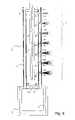
- FIG. 1shows a first embodiment of a thermal vapour deposition apparatus according to the invention allowing the deposition of a material on a substrate at a high rate.
- the apparatus of FIG. 1comprises material storage means 1 , which can for example be a melting crucible, for receiving the material to be melted and vaporized.
- the material storage means 1is heatable by heating means 2 , for example an electric heater, for heating the material stored in the material storage means 1 such that a vapour of the material is generated in the interior of the material storage means 1 .
- the material storage means 1can also be referred to as material storage container 1 .
- the heating means 2can also be referred to as heater 2 .
- the material storage means 1comprises corrosion-resistant surfaces being arranged to come into contact with the material vapour.
- the corrosion-resistant surfacescan be provided by means of a corrosion-resistant material such as quartz, fused silica, ceramic, graphite or carbon-fibre-enforced-carbon (CFC). These materials are able to withstand aggressive materials, in particular Se and Se vapour.
- a suitable ceramicis Al 2 O 3 .
- the surface but the entire wall or body of the material storage meanscan be of the corrosion-resistant material.
- the apparatus shown in FIG. 1further comprises vapour outlet means 3 which are arranged with respect to the material storage means 1 such that the vapour produced of the material stored in the material storage means 1 is received in the interior of the vapour outlet means 3 .
- the vapour outlet means 3have an elongated cylindrical shape.
- the vapour outlet means 3comprise a vapour receiving pipe 4 which has an opening at one end 4 a , forming an inlet for vapour of the vapour outlet means and vapour receiving pipe, such that the interior of the vapour receiving pipe 4 is in communication with the interior of the material storage means 1 to allow the material vapour to propagate from the material storage means 1 into the vapour outlet means 3 .
- the vapour receiving pipe 4has an elongated cylindrical shape.
- the vapour receiving pipe 4comprises vapour outlet passages 4 b allowing the material vapour to escape the vapour outlet means 3 in a direction towards a substrate 5 as indicated in FIG. 1 by means of grey triangles.
- the vapour receiving pipe 4comprises corrosion-resistant surfaces being arranged to come into contact with the material vapour.
- the surfaces, or in fact the entire wall or body of the vapour outlet means and vapour receiving pipe that are arranged to come into contact with the material vapourare made of corrosion-resistant material.
- the corrosion-resistant surfacescan be provided by means of a corrosion resistant material such as quartz, fused silica, ceramic, graphite or carbon-fibre-enforced-carbon (CFC).
- the vapour outlet means 3 of the apparatusfurther comprise emission reducing means 6 , for example an emission reducing pipe 6 as shown in FIG. 1 accommodating the vapour receiving pipe 4 in its interior, for reducing the emission of the vapour outlet means 4 at least in a direction towards the substrate 5 .
- emission reducing means 6Due to the provision of said emission reducing means 6 the heating of substrate 5 by radiation from the vapour outlet means 3 is reduced such that the temperature of the substrate can be kept at an acceptable level and that the material reaching the substrate is not re-vaporized from the surface of the substrate.
- the emission reducing means 6have an elongated cylindrical shape.
- the emission reducing means 6comprises corrosion-resistant surfaces being arranged to come into contact with the material vapour.
- the corrosion-resistant surfacescan be provided by means of a corrosion-resistant material such as fused silica, ceramic.
- the vapour receiving pipe 4 and/or the emission reducing means 6contribute to the gastightness of the vapour outlet means 3 , however depending on the material selected to different extents.
- the material selection according to this aspect of the inventionis performed such that the vapour receiving pipe 4 and/or the emission reducing means 6 cause the vapour outlet means 3 to be sufficiently gastight so that the gas pressure required for the material vapour to escape from the vapour outlet means 3 in order to propagate towards and reach the substrate 5 is obtained to a sufficient degree when the material is heated in the material storage means 1 of an apparatus according to the invention.
- the gastightness achieved according to a specific and separate aspect of the inventionprovides the vapour outlet means 3 with the capability to build up sufficient dynamic pressure for homogenous deposition of the vapour material.
- the gastightness mentioned abovecan be observed, for example by comparing the amount of material vapour escaping through the vapour outlet passages 4 b to the overall amount of material vapour generated in the thermal evaporation apparatus according to the invention.
- the vapour outlet meansis arranged such that 75% or more of the material vapour that is produced in the material storage means escape from the vapour outlet means 3 through the vapour outlet passages 4 b .
- the gastightnesscan be further increased such that 90% or more, or even at least 99% of the material vapour generated in an apparatus according the invention escape from the vapour outlet means 3 through the vapour outlet passages 4 b .
- a particularly suitable materialis high-density graphite, and coated CFC is another option.
- the emission reducing means 6are provided with vapour passage through holes 6 a at locations aligned with the vapour outlet passages 4 b of the vapour receiving pipe 4 so that the material vapour escaping from the vapour outlet means 3 through the vapour outlet passages 4 b in the vapour receiving pipe 4 can propagate essentially unhindered towards the substrate 5 .
- the diameter of the vapour passage through holes of the emission reducing means 6is equal or greater than the diameter of the vapour outlet passages 4 b of the vapour receiving pipe 4 .
- the apparatus shown in FIG. 1further comprises pipe heating means 7 , which in the embodiment shown is a line shaped pipe heating means arranged in the vapour receiving pipe 4 such that the longitudinal axes of the line shaped pipe heating means 7 and of the vapour receiving pipe 4 run parallel and preferably coincide.
- the line shaped heating means 7heat the vapour outlet means 3 and prevent the material vapour in the interior of the vapour outlet means 3 to condensate and/or to form droplets.
- the line shaped pipe heating means 7comprise a heating element 7 a and a heating element bulb (cover) 7 b in which the heating element 7 a is arranged.
- the heating element 7 a and the heating element bulb 7 bonly the latter has an outer surface which faces the interior of the vapour receiving pipe 4 and which comes into contact with the material vapour.
- the line shaped pipe heating means 7comprise an outer corrosion-resistant surface, for example provided by means of the above mentioned heating element bulb 7 b , wherein the corrosion-resistant surface is provided by means of a corrosion-resistant material such as quartz, fused silica, ceramic and graphite.
- the line shaped heating means 7is a tungsten halogenide IR heater, i.e. a tungsten halide lamp comprising electrical contacts, e.g. two electrical connectors 7 d , for supplying electric energy to said tungsten halide lamp.
- FIG. 2shows a cross-sectional view of the vapour outlet means 3 at line A-A shown in FIG. 1 .
- the emission reducing means 6are arranged to surround the vapour receiving pipe 4 and that the vapour outlet passages 4 b of the vapour receiving pipe 4 and vapour passage through holes 6 a of the emission reducing means 6 are arranged to allow the vapour to escape from the interior of the vapour outlet means 3 through said passages, in particular they are aligned.
- the vapour receiving pipe 4 and the emission reducing means 6preferably have a cylindrical cross-section.
- the vapour receiving pipe 4 , the emission reducing means 6 and the line shaped pipe heating means 7are arranged concentrically with respect to their longitudinal axes.
- the emission reducing pipe 6 as described aboveis shown comprising individual vapour passage through holes 6 a .
- the emission reducing means 6may be provided with an elongated vapour passage slit 6 b , as shown in FIG. 2 b , which is aligned with the vapour outlet passages 4 b of the vapour receiving pipe 4 .
- FIG. 3shows a second embodiment of a thermal vapour deposition apparatus according to the invention which is similar to the first embodiment in several aspects.
- the apparatus shown in FIG. 3comprises material storage means 1 for receiving the material to be melted and vaporized and heating means 2 for heating the material stored in the material storage means 1 .
- the apparatus according to the second embodimentcomprises vapour outlet means 3 which are arranged with respect to the material storage means 1 such that the vapour produced of the material stored in the material storage means 1 is received in the interior of the vapour outlet means 3 .
- FIG. 3shows a second embodiment of a thermal vapour deposition apparatus according to the invention which is similar to the first embodiment in several aspects.
- the apparatus shown in FIG. 3comprises material storage means 1 for receiving the material to be melted and vaporized and heating means 2 for heating the material stored in the material storage means 1 .
- the apparatus according to the second embodimentcomprises vapour outlet means 3 which are arranged with respect to the material storage means 1 such that the vapour produced of the material stored in the material storage means 1 is received
- the vapour outlet means 3comprise a vapour receiving pipe 4 having an open end portion 4 a and vapour outlet passages 4 b allowing the material vapour to escape the vapour outlet means 3 in a direction towards a substrate 5 .
- Line shaped pipe heating means 7are provided in the vapour outlet means 3 as shown in FIG. 3 .
- the second embodiment of the apparatus according to the inventionalso comprises emission reducing means 6 which are, however, provided by means of an emission reducing layer 6 on at least some portions of the surface of the vapour receiving pipe 4 .
- the emission reducing layer 6is arranged such that the vapour outlet passages 4 b of the vapour receiving pipe 4 are left open so that the vapour is not hindered from escaping from the interior of the vapour outlet means 3 in the apparatus according to the second embodiment of the invention as shown in FIG. 3 .
- FIG. 4is a cross-sectional view of the vapour outlet means 3 at line A-A shown in FIG. 3 . It is apparent from FIG. 4 that in the second embodiment of the apparatus according to the invention the emission reducing layer 6 is arranged on the surface of the vapour receiving pipe 4 and that the vapour outlet passages 4 b are open for the material vapour to pass through.
- FIG. 5shows an alternative arrangement of the emission reducing layer 6 of the second embodiment.
- the principle of the alternative arrangementis, however, applicable to the emission reducing means of any embodiment of the invention.
- the emission reducing layer 6 according to the alternative arrangementis provided only on a portion of the surface of the vapour receiving pipe 4 such that the surface portion of the vapour outlet means 3 facing the substrate 5 is covered by the emission reducing layer 6 .
- FIG. 6shows a third embodiment of the apparatus according to the invention.
- the apparatus according to the third embodimentcomprises all features of the apparatus according to the first embodiment so that reference is made to the respective description above.
- the apparatusfurther comprises radiation absorbing means 8 which are provided to absorb the heating radiation emitted by the line shaped pipe heating means 7 and to achieve an improved efficiency by keeping the energy in the vapour outlet means 3 to heat the material vapour.
- the absorption rate and in particular absorption coefficient of the radiation absorbing means 8is higher than the absorption rate and in particular absorption coefficient of the vapour receiving pipe 4 , respectively, and preferably exceeds 50%.
- the radiation absorbing meansis provided in the interior of the vapour outlet means and vapour outlet pipe.
- the radiation absorbing means 8are especially advantageous if the material of the vapour receiving pipe 4 is transparent to the radiation of the heating means to such an extent that the heating radiation emitted by the heating means of the vapour outlet means, such as line shaped pipe heating means 7 , may substantially pass the vapour receiving pipe 4 .
- the vapour receiving pipe 4is manufactured of a material such as quartz
- the radiation absorbing meansare made of a material such as CFC, graphite, TiN or SiN are particularly advantageous.
- the radiation absorbing meansthen absorbs the radiation energy from the heating means transmits thermal energy by radiating itself at different wavelengths that can be absorbed by the vapour receiving pipe, and/or by thermal conduction.
- the radiation absorbing means 8comprises corrosion-resistant surfaces being arranged to come into contact with the material vapour.
- the corrosion-resistant surfacescan be provided by means of a corrosion-resistant material such as ceramic, TiN, SiN, graphite or carbon-fibre-enforced-carbon (CFC).
- the radiation absorbing means 8may be provided by means of a radiation absorbing pipe 8 which is arranged in the interior of the vapour receiving pipe 4 of the vapour outlet means 3 .
- the radiation absorbing pipe 8may be in extensive contact with the vapour receiving pipe 4 or may be haltered such that the contact between the radiation absorbing pipe 8 and the vapour receiving pipe 4 only exist at some determined locations 8 a .
- the radiation absorbing means 8may be provided by means of a radiation absorbing layer which is provided on the interior surface of the vapour receiving pipe 4 in an arrangement similar to the emission reducing layer mentioned above.
- the radiation absorbing means 8comprise vapour passage through holes 8 b which are aligned with the vapour outlet passages 4 b of the vapour receiving pipe 4 to allow the vapour to escape substantially unhindered from the interior of the vapour outlet means 3 of an apparatus according to the invention.
- the radiation absorbing means 8may be provided by means of a radiation absorbing pipe which is arranged in the interior of the vapour outlet means 3 in the vicinity of the line shaped heating means 7 and which receives the line shaped heating means in its interior, respectively. Further, the radiation absorbing means 8 may be provided by means of a radiation absorbing layer on the surface of the line-shaped heating means 7 , which layer can be a coated layer. According to both alternatives, the radiation absorbing means 8 effectively can absorb the short wavelength IR radiation of the line-shaped heating means and send out long wavelength IR radiation (black body radiation). A short wavelength is a wavelength lower than an upper threshold of between 1 and 4 micrometer, such as below 2 micrometer.
- FIG. 7shows a cross-sectional view of the vapour outlet means 3 at line A-A shown in FIG. 6 .
- the radiation absorbing means 8are arranged to be surrounded by the vapour receiving pipe 4 and that the vapour outlet passages 4 b of the vapour receiving pipe 4 and vapour passage through holes 8 a of the radiation absorbing means 8 are arranged to allow the vapour to escape from the interior of the vapour outlet means 3 through said passages.
- the radiation absorbing means 8preferably have a cylindrical cross-section.
- the vapour receiving pipe 4 , the emission reducing means 6 , the line shaped pipe heating means 7 and the radiation absorbing means 8are arranged concentrically with respect to their longitudinal axes.
- the apparatuscomprises a valve means 9 , as shown by dashed lines in FIGS. 1 , 5 and 6 , arranged such that the interior of the vapour outlet means 3 can be shut to stop the evaporation through the vapour receiving pipe.
- the valve means 9consist of a corrosion-resistant material such as the materials mentioned above.
- the apparatuscomprises cooling means ( 2 a ) for fast cooling of the material storage means ( 1 ) and the material contained therein. Said cooling means allow for a fast stop of evaporation in case of a machine shut down and maintenance.
- the coolantcan be provided in form of a gas or liquid.
- the material storage meansis arranged to supply said vapour to an end portion of said vapour receiving pipe of said vapour outlet means, in particular to a lower end of an upright vapour receiving pipe.
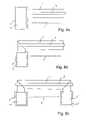
- FIGS. 8 a to 8 care schematic drawings of embodiments of the invention
- the material storage means 1 and the vapour receiving means 3may be arranged differently from the arrangement shown in FIGS. 1 , 5 and 6 .
- the vapour outlet means 3may be arranged at one side of the material storage means 1 .
- the vapour outlet means 3may be bent by any degree, for example by 90°.
- FIG. 8 athe vapour outlet means 3 may be bent by any degree, for example by 90°.
- second material storage means 1 ′ and second heating means 2 ′may be provided such that the first material storage means 1 and first heating means 2 are arranged at one end of the vapour outlet means 3 and the second material storage means 1 ′ and the second heating means 2 ′ are arranged at the respective other end of the vapour outlet means 3 .
- the position of the substrate 5is also indicated in FIGS. 8 a to 8 c .
- the second material storage meanscan be arranged at an end portion of the vapour receiving pipe.
- a corrosion resistant object, surface, or material in the description or in the claimsthis can in particular be a non-metallic object, surface, or material.
- a suitable corrosion-resistant ceramiccan be Al 2 O 3 .
- a measure for corrosion resistancecan be the weight increase of a material surface, such as in mg/cm 2 , in a defined atmosphere of a particular vapour pressure and constitution.
- a maximum weight increase of 5 mg/cm 2 ; preferably maximum 1 mg/cm 2is considered sufficiently corrosion resistant after being subjected to a Selenium atmosphere at a temperature between 300 and 600 degrees C. for 10 days.
- Graphite for examplewas found to exhibit less than 1 mg/cm 2 weight increase. For comparison, several steels that were tested exhibited 10-50 mg/cm 2 weight increase.
Landscapes
- Chemical & Material Sciences (AREA)
- Chemical Kinetics & Catalysis (AREA)
- Engineering & Computer Science (AREA)
- Materials Engineering (AREA)
- Mechanical Engineering (AREA)
- Metallurgy (AREA)
- Organic Chemistry (AREA)
- Health & Medical Sciences (AREA)
- Toxicology (AREA)
- Physical Vapour Deposition (AREA)
Abstract
Description
- The present invention relates to a thermal evaporation apparatus for deposition of various kinds of thin films on a substrate at a high deposition rate and more particularly to improvements regarding such an apparatus leading to a higher durability of the thermal evaporation apparatus, especially when aggressive materials, such as Selenium (Se) are deposited.
- For example, in the process of manufacturing a Cu(In,Ga)(S,Se)2semiconductor layer of a CIS solar module, the method of thermal vapour deposition (hereinafter referred to as “TVD”) is well established to deposit Selenium (Se) thin films on large surface substrates.
- In industrial production processes for manufacturing devices comprising a thin film of thermal vapour deposited material several general requirements have to be observed. For example, in order to be effective, an industrial manufacturing process requires a sufficiently high deposition rate which can be achieved when the TVD is performed at high temperatures. A further requirement relates to durability of the apparatus employed for TVD. The former requirement contradicts the latter since higher temperatures lead to higher wear and a reduced life cycle of the apparatus. In addition, higher temperatures increase the risk of contaminations of the material to be deposited by means of TVD, especially when aggressive materials such as Selenium (Se) are to be deposited. Particularly, in the field of solar cell semiconductor CIS thin films such contaminations may cause impurity traps in the semiconductor deteriorating the performance. Finally, high corrosion attack due to high processing temperatures makes it difficult to achieve constancy in apparatus performance which is a further requirement of industrial manufacturing processes.
- DE 100 21 530 C1 describes a vapour source with an elongated vapour outlet pipe and a heating rod provided coaxially in the interior of the vapour outlet pipe. The vapour source of DE 100 21 530 C1 is specifically designed for the manufacturing process of CIS thin film solar cells. The material to be deposited is heated in two crucibles whereby a vapour is generated and the vapour is supplied to the heated vapour outlet pipe comprising outlet openings through which the vapour escapes from the vapour source for being deposited on a substrate. It is mentioned in DE 100 21 530 C1 that several vapour sources can be used in a serial arrangement to deposit different materials in the manufacturing process of a CIS solar cell.
- EP 1 424 404 A describes a thermal evaporation apparatus comprising an electrically heated melting crucible in which the material to be deposited is stored and melted to generate the vapour. The vapour is received in a vapour pipe comprising outlet openings allowing the vapour to escape from the vapour pipe. The vapour pipe is surrounded by a heater, and radiation reflectors are arranged in order to direct the heat provided by the heater to the vapour pipe.
- There is a need for a thermal evaporation apparatus which is capable of depositing any material, including aggressive materials, such as Selenium (Se), at high deposition rates.
- There is also a need for a thermal evaporation apparatus which can be operated at high temperatures up to and above 400° C., and even much higher, in order to achieve high deposition rates.
- There is further a need for a thermal evaporation apparatus which is resistant to wear even at high temperatures and in the presence of aggressive materials such as Selenium (Se).
- There is a still further need for a thermal evaporation apparatus which is specifically suited for being employed in the manufacturing process of CIS solar cells.
- The invention provides a thermal evaporation apparatus for depositing a material on a substrate, the apparatus comprising
- material storage means for receiving the material to be deposited, wherein at least the surfaces of the material storage means arranged to come into contact with the material vapour are of a corrosion-resistant material, for example a material of the group consisting of but not being limited to quartz, fused silica, ceramic, graphite and carbon-fibre-enforced-carbon (CFC);
- heating means for heating the material in the material storage means to generate a vapour of the material;
- vapour outlet means arranged to receive in its interior the vapour of the material heated in said material storage means, said vapour outlet means comprising
- a vapour receiving pipe having vapour outlet passages, wherein at least the surfaces of the vapour receiving pipe arranged to come into contact with the material vapour are of a corrosion-resistant material, for example a material of the group consisting of but not being limited to quartz, fused silica, ceramic, graphite and carbon-fibre-enforced-carbon (CFC), and
- emission reducing means arranged such that an external surface of the vapour outlet means directed to said substrate exhibits low emission, wherein at least the surfaces of the emission reducing means arranged to come into contact with the material vapour are of a corrosion-resistant material, for example a material of the group consisting of but not being limited to fused silica and ceramic, and wherein the apparatus further comprises
- pipe heating means arranged in the interior of said vapour outlet means, preferably being a line shaped pipe heating means extending along or in parallel with a longitudinal axis of said vapour receiving pipe, said pipe heating means being provided with an outer corrosion-resistant surface arranged to come into contact with the material vapour and being formed of a corrosion-resistant material, for example a material of the group consisting of but not being limited to quartz, fused silica, ceramic, and graphite.
- The above thermal evaporation apparatus is also described in claim1. Advantageous embodiments are described in the subclaims.
- The thermal evaporation apparatus allows to deposit aggressive materials, such as Selenium (Se), at high deposition rates. Surfaces of components that come in contact with the vapour are of a corrosion-resistant material.
- A particular advantage is achieved by the emission reducing means, which allows to reduce the thermal emission of the vapour outlet means at least in a direction towards the substrate, so that heating of substrate by radiation from the vapour outlet means is reduced to an acceptable level and that the material reaching the substrate is not re-vaporized from the surface of the substrate, even if the vapour outlet means is operated at high temperatures such as above 350° C., 400° C., or higher than 400° C. The apparatus can with advantage be used in the manufacturing process of CIS solar cells, and in particular for depositing Selenium on a precursor of a CIS thin film. Such a precursor comprises a sequence of layers of different chemical composition, with constituents of the CIS layer to be formed. After deposition of Selenium, the precursor has to undergo thermal processing in order to form the CIS layer. During Selenium deposition, the temperature of the substrate with the precursor preferably does not exceed a certain maximum temperature. The maximum temperature is determined taking the sticking coefficient of Selenium into account, which sticking coefficient is a measure of the balance between deposition and re-evaporation. A suitable maximum temperature for Selenium deposition is 90 degrees C., preferably 80 degrees C., more preferably 70 degrees C.
- The emission reducing means suitably exhibits low emission in that it includes or is made from a material having a low emissivity. Emissivity of a material is the ratio of energy radiated by the material to the energy radiated by a black body of the same temperature, and is typically denoted as ε, a dimensionless number between 0 and 1. ε=1 is a black body. Suitably the emissivity of the emission reducing means is 0.6 or less, preferably 0.5 or less, more preferably 0.3 or less. Of particular relevance is the emission and emissivity in the direction of the substrate during normal operation.
- The thermal evaporation apparatus for depositing a material on a substrate according to another aspect of the invention comprises
- material storage means for receiving the material to be deposited, said material storage means consisting of a corrosion-resistant material, for example a material of the group consisting of but not being limited to quartz, fused silica, ceramic, graphite and carbon-fibre-enforced-carbon (CFC);
- heating means for heating the material in the material storage means to generate a vapour of the material; and
- vapour outlet means arranged to receive in its interior the vapour of the material heated in said material storage means and having vapour outlet passages, wherein said vapour outlet means basically consist of a corrosion-resistant material, for example a material of the group consisting of but not being limited to quartz, fused silica, ceramic, graphite and carbon-fibre-enforced-carbon (CFC) and wherein said vapour outlet means are gastight to such an extent that sufficient dynamic pressure of said material vapour is achievable for homogenous deposition of said material on said substrate.
- The above thermal evaporation apparatus is also described in claim21. Advantageous embodiments are described in the subclaims.
- A further advantage of the invention is that the vapour outlet is sufficiently gastight for the evaporation material, such as aggressive Se vapour. This also allows to build up sufficient dynamic pressure for homogenous deposition of the vapour material.
- The invention is further directed to the use of a thermal evaporation apparatus of the invention for depositing a material on a substrate, in particular wherein the material is Selenium, and more in particular wherein the substrate comprises a precursor or precursor layers of a CIS layer.
- The invention moreover provides a method of depositing a material onto a substrate by thermal evaporation, the method comprising
- providing a thermal evaporation apparatus comprising heatable material storage means for receiving the material to be deposited; and heatable vapour outlet means arranged to receive in its interior the vapour of the material heated in said material storage means and having vapour outlet passages;
- selecting a maximum temperature of the substrate during thermal evaporation of the material;
- providing emission reducing means for the vapour outlet means, which emission reducing means are arranged such that an external surface of the vapour outlet means directed to said substrate exhibits emission that is low enough such that the substrate will not be heated above the maximum temperature during thermal evaporation of the material; and
- operating the thermal evaporation apparatus including heating the material storage means and vapour outlet means so as to evaporate and deposit the material on the substrate.
- The maximum temperature is selected taking a parameter related to re-evaporation of the deposited material from the substrate, such as a sticking coefficient, into account, and/or taking thermal stability of the substrate or part thereof into account.
- In a particular embodiment the material is Selenium, and more in particular the substrate comprises a precursor or precursor layers of a CIS layer in thermal equilibrium, e.g. Cu, In, Ga, and/or binary layers such as Cu/Ga or In/Ga. The latter case is to be distinguished from CIS layer formation by co-evaporation of CIS constituents onto a hot substrate such as discussed for example in U.S. Pat. No. 7,194,197. In co-evaporation the substrate is kept at a much higher temperature than when depositing a layer on a CIS precursor, because CIS film formation takes place simultaneously with deposition. Therefore it is specific for the deposition on a CIS precursor layer that the thermal energy emitted by the evaporation apparatus towards the typically much colder substrate is an issue. In the method of the invention the substrate therefore preferably does not comprise a CIS precursor layer.
- In the following embodiments of the invention will be described in more detail and with reference to the drawings, wherein
FIG. 1 shows a first embodiment of a thermal vapour deposition apparatus according to the invention;FIG. 2 shows a cross-sectional view of the first embodiment of a thermal vapour deposition apparatus according to the invention;FIG. 2 ashows a perspective view of a first variant of an emission reducing pipe of the first embodiment of a thermal vapour deposition apparatus according to the invention;FIG. 2 bshows a perspective view of a second variant of an emission reducing pipe of the first embodiment of a thermal vapour deposition apparatus according to the invention;FIG. 3 shows a second embodiment of a thermal vapour deposition apparatus according to the invention;FIG. 4 shows a cross-sectional view of the second embodiment of a thermal vapour deposition apparatus according to the invention;FIG. 5 shows a cross-sectional view of an alternative arrangement of the emission reducing means of any of the embodiments of a thermal vapour deposition apparatus according to the invention;FIG. 6 shows a third embodiment of a thermal vapour deposition apparatus according to the invention;FIG. 7 shows a cross-sectional view of the third embodiment of a thermal vapour deposition apparatus according to the invention; andFIGS. 8 ato8cshow different arrangements of the vapour outlet means with respect to the material storage means of a thermal vapour deposition apparatus according to the invention.- Where the same reference numerals are used in different Figures, they refer to the same or similar objects.
- Reference is made to
FIG. 1 .FIG. 1 shows a first embodiment of a thermal vapour deposition apparatus according to the invention allowing the deposition of a material on a substrate at a high rate. The apparatus ofFIG. 1 comprises material storage means1, which can for example be a melting crucible, for receiving the material to be melted and vaporized. The material storage means1 is heatable by heating means2, for example an electric heater, for heating the material stored in the material storage means1 such that a vapour of the material is generated in the interior of the material storage means1. The material storage means1 can also be referred to as material storage container1. The heating means2 can also be referred to asheater 2. - The material storage means1 comprises corrosion-resistant surfaces being arranged to come into contact with the material vapour. The corrosion-resistant surfaces can be provided by means of a corrosion-resistant material such as quartz, fused silica, ceramic, graphite or carbon-fibre-enforced-carbon (CFC). These materials are able to withstand aggressive materials, in particular Se and Se vapour. A suitable ceramic is Al2O3. Clearly, not only the surface but the entire wall or body of the material storage means can be of the corrosion-resistant material.
- The apparatus shown in
FIG. 1 further comprises vapour outlet means3 which are arranged with respect to the material storage means1 such that the vapour produced of the material stored in the material storage means1 is received in the interior of the vapour outlet means3. Preferably, the vapour outlet means3 have an elongated cylindrical shape. - The vapour outlet means3 comprise a
vapour receiving pipe 4 which has an opening at oneend 4a, forming an inlet for vapour of the vapour outlet means and vapour receiving pipe, such that the interior of thevapour receiving pipe 4 is in communication with the interior of the material storage means1 to allow the material vapour to propagate from the material storage means1 into the vapour outlet means3. Preferably, thevapour receiving pipe 4 has an elongated cylindrical shape. As shown inFIG. 1 , thevapour receiving pipe 4 comprisesvapour outlet passages 4ballowing the material vapour to escape the vapour outlet means3 in a direction towards asubstrate 5 as indicated inFIG. 1 by means of grey triangles. - According to the invention, the
vapour receiving pipe 4 comprises corrosion-resistant surfaces being arranged to come into contact with the material vapour. The surfaces, or in fact the entire wall or body of the vapour outlet means and vapour receiving pipe that are arranged to come into contact with the material vapour are made of corrosion-resistant material. The corrosion-resistant surfaces can be provided by means of a corrosion resistant material such as quartz, fused silica, ceramic, graphite or carbon-fibre-enforced-carbon (CFC). - The vapour outlet means3 of the apparatus, according a specific and separate aspect of the invention, further comprise emission reducing means6, for example an emission reducing pipe6 as shown in
FIG. 1 accommodating thevapour receiving pipe 4 in its interior, for reducing the emission of the vapour outlet means4 at least in a direction towards thesubstrate 5. Due to the provision of said emission reducing means6 the heating ofsubstrate 5 by radiation from the vapour outlet means3 is reduced such that the temperature of the substrate can be kept at an acceptable level and that the material reaching the substrate is not re-vaporized from the surface of the substrate. Preferably, the emission reducing means6 have an elongated cylindrical shape. - The emission reducing means6 comprises corrosion-resistant surfaces being arranged to come into contact with the material vapour. The corrosion-resistant surfaces can be provided by means of a corrosion-resistant material such as fused silica, ceramic.
- By selecting a combination of materials for the
vapour receiving pipe 4 and the emission reducing means6 appropriate for a specific application, thevapour receiving pipe 4 and/or the emission reducing means6 contribute to the gastightness of the vapour outlet means3, however depending on the material selected to different extents. In any case, the material selection according to this aspect of the invention is performed such that thevapour receiving pipe 4 and/or the emission reducing means6 cause the vapour outlet means3 to be sufficiently gastight so that the gas pressure required for the material vapour to escape from the vapour outlet means3 in order to propagate towards and reach thesubstrate 5 is obtained to a sufficient degree when the material is heated in the material storage means1 of an apparatus according to the invention. The gastightness achieved according to a specific and separate aspect of the invention provides the vapour outlet means3 with the capability to build up sufficient dynamic pressure for homogenous deposition of the vapour material. - The gastightness mentioned above can be observed, for example by comparing the amount of material vapour escaping through the
vapour outlet passages 4bto the overall amount of material vapour generated in the thermal evaporation apparatus according to the invention. In a preferred embodiment, the vapour outlet means is arranged such that 75% or more of the material vapour that is produced in the material storage means escape from the vapour outlet means3 through thevapour outlet passages 4b. According to the invention, the gastightness can be further increased such that 90% or more, or even at least 99% of the material vapour generated in an apparatus according the invention escape from the vapour outlet means3 through thevapour outlet passages 4b. A particularly suitable material is high-density graphite, and coated CFC is another option. - The emission reducing means6 are provided with vapour passage through
holes 6aat locations aligned with thevapour outlet passages 4bof thevapour receiving pipe 4 so that the material vapour escaping from the vapour outlet means3 through thevapour outlet passages 4bin thevapour receiving pipe 4 can propagate essentially unhindered towards thesubstrate 5. For this purpose, the diameter of the vapour passage through holes of the emission reducing means6 is equal or greater than the diameter of thevapour outlet passages 4bof thevapour receiving pipe 4. - According to the invention, the apparatus shown in
FIG. 1 further comprises pipe heating means7, which in the embodiment shown is a line shaped pipe heating means arranged in thevapour receiving pipe 4 such that the longitudinal axes of the line shaped pipe heating means7 and of thevapour receiving pipe 4 run parallel and preferably coincide. The line shaped heating means7 heat the vapour outlet means3 and prevent the material vapour in the interior of the vapour outlet means3 to condensate and/or to form droplets. - In the embodiment shown in
FIG. 1 , the line shaped pipe heating means7 comprise a heating element7aand a heating element bulb (cover)7bin which the heating element7ais arranged. Of the heating element7aand the heating element bulb7bonly the latter has an outer surface which faces the interior of thevapour receiving pipe 4 and which comes into contact with the material vapour. - According to the invention, the line shaped pipe heating means7 comprise an outer corrosion-resistant surface, for example provided by means of the above mentioned heating element bulb7b, wherein the corrosion-resistant surface is provided by means of a corrosion-resistant material such as quartz, fused silica, ceramic and graphite.
- Advantageously, the line shaped heating means7 is a tungsten halogenide IR heater, i.e. a tungsten halide lamp comprising electrical contacts, e.g. two
electrical connectors 7d, for supplying electric energy to said tungsten halide lamp. FIG. 2 shows a cross-sectional view of the vapour outlet means3 at line A-A shown inFIG. 1 . It is apparent fromFIG. 2 that the emission reducing means6 are arranged to surround thevapour receiving pipe 4 and that thevapour outlet passages 4bof thevapour receiving pipe 4 and vapour passage throughholes 6aof the emission reducing means6 are arranged to allow the vapour to escape from the interior of the vapour outlet means3 through said passages, in particular they are aligned. As can be taken fromFIG. 2 , thevapour receiving pipe 4 and the emission reducing means6 preferably have a cylindrical cross-section. It is further apparent that in the shown embodiment of the invention thevapour receiving pipe 4, the emission reducing means6 and the line shaped pipe heating means7 are arranged concentrically with respect to their longitudinal axes.- In
FIG. 2 athe emission reducing pipe6 as described above is shown comprising individual vapour passage throughholes 6a. It should be noted that instead of the individual vapour passage throughholes 6aas described above the emission reducing means6 may be provided with an elongated vapour passage slit6b, as shown inFIG. 2 b, which is aligned with thevapour outlet passages 4bof thevapour receiving pipe 4. FIG. 3 shows a second embodiment of a thermal vapour deposition apparatus according to the invention which is similar to the first embodiment in several aspects. Accordingly, the apparatus shown inFIG. 3 comprises material storage means1 for receiving the material to be melted and vaporized and heating means2 for heating the material stored in the material storage means1. Further, the apparatus according to the second embodiment comprises vapour outlet means3 which are arranged with respect to the material storage means1 such that the vapour produced of the material stored in the material storage means1 is received in the interior of the vapour outlet means3. As shown inFIG. 3 the vapour outlet means3 comprise avapour receiving pipe 4 having anopen end portion 4aandvapour outlet passages 4ballowing the material vapour to escape the vapour outlet means3 in a direction towards asubstrate 5. Line shaped pipe heating means7 are provided in the vapour outlet means3 as shown inFIG. 3 . For further details of the second embodiment of the apparatus according to the invention reference is made to the above description of the first embodiment.- The second embodiment of the apparatus according to the invention also comprises emission reducing means6 which are, however, provided by means of an emission reducing layer6 on at least some portions of the surface of the
vapour receiving pipe 4. The emission reducing layer6 is arranged such that thevapour outlet passages 4bof thevapour receiving pipe 4 are left open so that the vapour is not hindered from escaping from the interior of the vapour outlet means3 in the apparatus according to the second embodiment of the invention as shown inFIG. 3 . FIG. 4 is a cross-sectional view of the vapour outlet means3 at line A-A shown inFIG. 3 . It is apparent fromFIG. 4 that in the second embodiment of the apparatus according to the invention the emission reducing layer6 is arranged on the surface of thevapour receiving pipe 4 and that thevapour outlet passages 4bare open for the material vapour to pass through.FIG. 5 shows an alternative arrangement of the emission reducing layer6 of the second embodiment. The principle of the alternative arrangement is, however, applicable to the emission reducing means of any embodiment of the invention. As is apparent fromFIG. 5 , the emission reducing layer6 according to the alternative arrangement is provided only on a portion of the surface of thevapour receiving pipe 4 such that the surface portion of the vapour outlet means3 facing thesubstrate 5 is covered by the emission reducing layer6.FIG. 6 shows a third embodiment of the apparatus according to the invention. The apparatus according to the third embodiment comprises all features of the apparatus according to the first embodiment so that reference is made to the respective description above. However, according to the third embodiment, the apparatus further comprisesradiation absorbing means 8 which are provided to absorb the heating radiation emitted by the line shaped pipe heating means7 and to achieve an improved efficiency by keeping the energy in the vapour outlet means3 to heat the material vapour. To achieve the desired increase in efficiency, the absorption rate and in particular absorption coefficient of theradiation absorbing means 8 is higher than the absorption rate and in particular absorption coefficient of thevapour receiving pipe 4, respectively, and preferably exceeds 50%. The radiation absorbing means is provided in the interior of the vapour outlet means and vapour outlet pipe.- The
radiation absorbing means 8 are especially advantageous if the material of thevapour receiving pipe 4 is transparent to the radiation of the heating means to such an extent that the heating radiation emitted by the heating means of the vapour outlet means, such as line shaped pipe heating means7, may substantially pass thevapour receiving pipe 4. For example, if thevapour receiving pipe 4 is manufactured of a material such as quartz, the radiation absorbing means are made of a material such as CFC, graphite, TiN or SiN are particularly advantageous. The radiation absorbing means then absorbs the radiation energy from the heating means transmits thermal energy by radiating itself at different wavelengths that can be absorbed by the vapour receiving pipe, and/or by thermal conduction. Generally, according to the invention, theradiation absorbing means 8 comprises corrosion-resistant surfaces being arranged to come into contact with the material vapour. The corrosion-resistant surfaces can be provided by means of a corrosion-resistant material such as ceramic, TiN, SiN, graphite or carbon-fibre-enforced-carbon (CFC). - As shown in
FIG. 6 , theradiation absorbing means 8 may be provided by means of aradiation absorbing pipe 8 which is arranged in the interior of thevapour receiving pipe 4 of the vapour outlet means3. Theradiation absorbing pipe 8 may be in extensive contact with thevapour receiving pipe 4 or may be haltered such that the contact between theradiation absorbing pipe 8 and thevapour receiving pipe 4 only exist at some determined locations8a. Alternatively, theradiation absorbing means 8 may be provided by means of a radiation absorbing layer which is provided on the interior surface of thevapour receiving pipe 4 in an arrangement similar to the emission reducing layer mentioned above. In any case, theradiation absorbing means 8 comprise vapour passage through holes8bwhich are aligned with thevapour outlet passages 4bof thevapour receiving pipe 4 to allow the vapour to escape substantially unhindered from the interior of the vapour outlet means3 of an apparatus according to the invention. - According to an alternative embodiment, the
radiation absorbing means 8 may be provided by means of a radiation absorbing pipe which is arranged in the interior of the vapour outlet means3 in the vicinity of the line shaped heating means7 and which receives the line shaped heating means in its interior, respectively. Further, theradiation absorbing means 8 may be provided by means of a radiation absorbing layer on the surface of the line-shaped heating means7, which layer can be a coated layer. According to both alternatives, theradiation absorbing means 8 effectively can absorb the short wavelength IR radiation of the line-shaped heating means and send out long wavelength IR radiation (black body radiation). A short wavelength is a wavelength lower than an upper threshold of between 1 and 4 micrometer, such as below 2 micrometer. FIG. 7 shows a cross-sectional view of the vapour outlet means3 at line A-A shown inFIG. 6 . It is apparent fromFIG. 7 that theradiation absorbing means 8 are arranged to be surrounded by thevapour receiving pipe 4 and that thevapour outlet passages 4bof thevapour receiving pipe 4 and vapour passage through holes8aof theradiation absorbing means 8 are arranged to allow the vapour to escape from the interior of the vapour outlet means3 through said passages. As can be taken fromFIG. 7 , theradiation absorbing means 8 preferably have a cylindrical cross-section. It is further apparent that in the shown embodiments of the invention thevapour receiving pipe 4, the emission reducing means6, the line shaped pipe heating means7 and theradiation absorbing means 8 are arranged concentrically with respect to their longitudinal axes.- Further, according to an advantageous embodiment of the invention, the apparatus comprises a valve means9, as shown by dashed lines in
FIGS. 1 ,5 and6, arranged such that the interior of the vapour outlet means3 can be shut to stop the evaporation through the vapour receiving pipe. - According to the invention, the valve means9 consist of a corrosion-resistant material such as the materials mentioned above. Further, according to another advantageous embodiment of the invention, the apparatus comprises cooling means (2a) for fast cooling of the material storage means (1) and the material contained therein. Said cooling means allow for a fast stop of evaporation in case of a machine shut down and maintenance. The coolant can be provided in form of a gas or liquid.
- In the embodiments of a thermal evaporation apparatus of the invention discussed so far, the material storage means is arranged to supply said vapour to an end portion of said vapour receiving pipe of said vapour outlet means, in particular to a lower end of an upright vapour receiving pipe.
- As shown in
FIGS. 8 ato8c, which are schematic drawings of embodiments of the invention, it should be noted that the material storage means1 and the vapour receiving means3 may be arranged differently from the arrangement shown inFIGS. 1 ,5 and6. As shown inFIG. 8 athe vapour outlet means3 may be arranged at one side of the material storage means1. As shown inFIG. 8 bthe vapour outlet means3 may be bent by any degree, for example by 90°. As shown inFIG. 8 c, second material storage means1′ and second heating means2′ may be provided such that the first material storage means1 and first heating means2 are arranged at one end of the vapour outlet means3 and the second material storage means1′ and the second heating means2′ are arranged at the respective other end of the vapour outlet means3. The position of thesubstrate 5 is also indicated inFIGS. 8 ato8c. Thus, the second material storage means can be arranged at an end portion of the vapour receiving pipe. - Where reference is made to a corrosion resistant object, surface, or material in the description or in the claims, this can in particular be a non-metallic object, surface, or material. A suitable corrosion-resistant ceramic can be Al2O3. A measure for corrosion resistance can be the weight increase of a material surface, such as in mg/cm2, in a defined atmosphere of a particular vapour pressure and constitution. For a selenium evaporator, a maximum weight increase of 5 mg/cm2; preferably maximum 1 mg/cm2, is considered sufficiently corrosion resistant after being subjected to a Selenium atmosphere at a temperature between 300 and 600 degrees C. for 10 days. Graphite for example was found to exhibit less than 1 mg/cm2weight increase. For comparison, several steels that were tested exhibited 10-50 mg/cm2weight increase.
Claims (16)
Applications Claiming Priority (4)
| Application Number | Priority Date | Filing Date | Title |
|---|---|---|---|
| EP06112796 | 2006-04-20 | ||
| EP06112796.5 | 2006-04-20 | ||
| EP06112796 | 2006-04-20 | ||
| PCT/EP2007/053912WO2007122203A2 (en) | 2006-04-20 | 2007-04-20 | Thermal evaporation apparatus, use and method of depositing a material |
Related Parent Applications (1)
| Application Number | Title | Priority Date | Filing Date |
|---|---|---|---|
| PCT/EP2007/053912A-371-Of-InternationalWO2007122203A2 (en) | 2006-04-20 | 2007-04-20 | Thermal evaporation apparatus, use and method of depositing a material |
Related Child Applications (1)
| Application Number | Title | Priority Date | Filing Date |
|---|---|---|---|
| US13/276,223DivisionUS8336489B2 (en) | 2006-04-20 | 2011-10-18 | Thermal evaporation apparatus, use and method of depositing a material |
Publications (2)
| Publication Number | Publication Date |
|---|---|
| US20090130794A1true US20090130794A1 (en) | 2009-05-21 |
| US8082878B2 US8082878B2 (en) | 2011-12-27 |
Family
ID=38523458
Family Applications (2)
| Application Number | Title | Priority Date | Filing Date |
|---|---|---|---|
| US12/297,527Expired - Fee RelatedUS8082878B2 (en) | 2006-04-20 | 2007-04-20 | Thermal evaporation apparatus, use and method of depositing a material |
| US13/276,223Expired - Fee RelatedUS8336489B2 (en) | 2006-04-20 | 2011-10-18 | Thermal evaporation apparatus, use and method of depositing a material |
Family Applications After (1)
| Application Number | Title | Priority Date | Filing Date |
|---|---|---|---|
| US13/276,223Expired - Fee RelatedUS8336489B2 (en) | 2006-04-20 | 2011-10-18 | Thermal evaporation apparatus, use and method of depositing a material |
Country Status (4)
| Country | Link |
|---|---|
| US (2) | US8082878B2 (en) |
| EP (1) | EP2007915A2 (en) |
| CN (1) | CN101454478A (en) |
| WO (1) | WO2007122203A2 (en) |
Cited By (9)
| Publication number | Priority date | Publication date | Assignee | Title |
|---|---|---|---|---|
| US20090305449A1 (en)* | 2007-12-06 | 2009-12-10 | Brent Bollman | Methods and Devices For Processing A Precursor Layer In a Group VIA Environment |
| US20120024228A1 (en)* | 2010-08-02 | 2012-02-02 | Sang-Woo Lee | Apparatus for forming thin film |
| WO2013096754A1 (en)* | 2011-12-23 | 2013-06-27 | Applied Materials, Inc. | Self-contained heating element |
| US8586401B2 (en) | 2010-10-14 | 2013-11-19 | Samsung Sdi Co., Ltd. | Gas injection device and solar cell manufacturing method using the same |
| US20140345527A1 (en)* | 2010-12-24 | 2014-11-27 | Sharp Kabushiki Kaisha | Vapor deposition device, vapor deposition method, and method of manufacturing organic electroluminescent display device |
| US20150187629A1 (en)* | 2013-12-31 | 2015-07-02 | Lam Research Ag | Apparatus for treating surfaces of wafer-shaped articles |
| US20150187624A1 (en)* | 2013-12-31 | 2015-07-02 | Lam Research Ag | Apparatus for treating surfaces of wafer-shaped articles |
| CN112368813A (en)* | 2018-06-14 | 2021-02-12 | 应用材料公司 | Vaporizer for depositing material on substrate, method of forming vaporizer, and vaporization apparatus for depositing material on flexible substrate |
| US20220025509A1 (en)* | 2019-02-27 | 2022-01-27 | Samsung Display Co., Ltd. | Deposition source evaporating apparatus and manufacturing method thereof |
Families Citing this family (8)
| Publication number | Priority date | Publication date | Assignee | Title |
|---|---|---|---|---|
| WO2012046672A1 (en)* | 2010-10-04 | 2012-04-12 | 東京エレクトロン株式会社 | Deposition apparatus and deposition material supply method |
| CN103380486B (en)* | 2010-12-21 | 2016-08-10 | 株式会社渡边商行 | carburetor |
| CN102839352A (en)* | 2011-06-21 | 2012-12-26 | 无锡尚德太阳能电力有限公司 | Film deposition device and method |
| DE102014007522A1 (en)* | 2014-05-23 | 2015-11-26 | Manz Ag | Carrier arrangement for an evaporator source |
| DE102014007521A1 (en)* | 2014-05-23 | 2015-11-26 | Manz Ag | Evaporator source for the surface treatment of substrates |
| US20160305009A1 (en)* | 2015-04-16 | 2016-10-20 | China Triumph International Engineering Co., Ltd. | Aperture with Optimized Thermal Emission Behavior |
| JP6488400B2 (en)* | 2015-07-13 | 2019-03-20 | アプライド マテリアルズ インコーポレイテッドApplied Materials,Incorporated | Evaporation source |
| WO2019084125A1 (en)* | 2017-10-26 | 2019-05-02 | First Solar, Inc. | Systems and methods for vaporization and vapor distribution |
Citations (27)
| Publication number | Priority date | Publication date | Assignee | Title |
|---|---|---|---|---|
| US2621296A (en)* | 1944-09-02 | 1952-12-09 | Robert W Thompson | Ion source |
| US2624845A (en)* | 1944-09-02 | 1953-01-06 | Robert W Thompson | Ion source |
| US3968346A (en)* | 1973-06-01 | 1976-07-06 | Cooksley Ralph D | Method and apparatus for electrically heating a fluid |
| US4662981A (en)* | 1983-02-23 | 1987-05-05 | Koito Seisakusho Co., Ltd. | Method and apparatus for forming crystalline films of compounds |
| US4854264A (en)* | 1986-12-10 | 1989-08-08 | Fuji Seiki Inc. | Vacuum evaporating apparatus |
| US5016566A (en)* | 1988-05-31 | 1991-05-21 | Levchenko Georgy T | Apparatus for forming films by evaporation in vacuum |
| US5019531A (en)* | 1988-05-23 | 1991-05-28 | Nippon Telegraph And Telephone Corporation | Process for selectively growing thin metallic film of copper or gold |
| US5284519A (en)* | 1990-05-16 | 1994-02-08 | Simon Fraser University | Inverted diffuser stagnation point flow reactor for vapor deposition of thin films |
| US5303671A (en)* | 1992-02-07 | 1994-04-19 | Tokyo Electron Limited | System for continuously washing and film-forming a semiconductor wafer |
| US5433791A (en)* | 1994-05-26 | 1995-07-18 | Hughes Aircraft Company | MBE apparatus with photo-cracker cell |
| US5462014A (en)* | 1990-03-09 | 1995-10-31 | Nippon Telegraph And Telephone Corporation | Apparatus for growing a thin metallic film |
| US5551984A (en)* | 1993-12-10 | 1996-09-03 | Tokyo Electron Kabushiki Kaisha | Vertical heat treatment apparatus with a circulation gas passage |
| US5722588A (en)* | 1994-04-13 | 1998-03-03 | Nippon Soken Inc. | Combustion heater |
| US6004885A (en)* | 1991-12-26 | 1999-12-21 | Canon Kabushiki Kaisha | Thin film formation on semiconductor wafer |
| US6036783A (en)* | 1996-04-05 | 2000-03-14 | Ebara Corporation | Liquid material vaporizer apparatus and gas ejection device |
| US6110283A (en)* | 1997-03-17 | 2000-08-29 | Mitsubishi Denki Kabushiki Kaisha | Chemical vapor deposition apparatus |
| US6148764A (en)* | 1997-12-29 | 2000-11-21 | Jet Process Corporation | Multiple micro inlet silane injection system for the jet vapor deposition of silicon nitride with a microwave discharge jet source |
| US20010011524A1 (en)* | 1998-11-12 | 2001-08-09 | Witzman Matthew R. | Linear aperture deposition apparatus and coating process |
| US6365016B1 (en)* | 1999-03-17 | 2002-04-02 | General Electric Company | Method and apparatus for arc plasma deposition with evaporation of reagents |
| US6397936B1 (en)* | 1999-05-14 | 2002-06-04 | Creare Inc. | Freeze-tolerant condenser for a closed-loop heat-transfer system |
| US6575178B1 (en)* | 1997-07-17 | 2003-06-10 | Tokyo Electron Limited | Cleaning and drying method and apparatus |
| US20040163600A1 (en)* | 2002-11-30 | 2004-08-26 | Uwe Hoffmann | Vapor deposition device |
| US20050208216A1 (en)* | 2004-03-22 | 2005-09-22 | Michael Long | High thickness uniformity vaporization source |
| US6948362B2 (en)* | 2002-07-16 | 2005-09-27 | Gralenski Nicholas M | Flow measurement device |
| US7194197B1 (en)* | 2000-03-16 | 2007-03-20 | Global Solar Energy, Inc. | Nozzle-based, vapor-phase, plume delivery structure for use in production of thin-film deposition layer |
| US20090047204A1 (en)* | 2006-08-10 | 2009-02-19 | Hee Young Kim | Method and Apparatus for Preparation of Granular Polysilicon |
| US7779785B2 (en)* | 2005-02-17 | 2010-08-24 | Hitachi Kokusai Electric Inc. | Production method for semiconductor device and substrate processing apparatus |
Family Cites Families (3)
| Publication number | Priority date | Publication date | Assignee | Title |
|---|---|---|---|---|
| JPS5943873A (en) | 1982-09-04 | 1984-03-12 | Konishiroku Photo Ind Co Ltd | Vessel for storing material to be evaporated |
| US5945163A (en) | 1998-02-19 | 1999-08-31 | First Solar, Llc | Apparatus and method for depositing a material on a substrate |
| DE10021530C1 (en) | 2000-05-03 | 2001-09-27 | Zsw | Vapor supply for thermal vapor deposition has heated crucibles at the axial ends of the vapor outlet pipe with passage openings into the pipe interior for easy crucible topping-up and trouble-free deposition |
- 2007
- 2007-04-20EPEP07728369Apatent/EP2007915A2/ennot_activeWithdrawn
- 2007-04-20CNCNA2007800193286Apatent/CN101454478A/enactivePending
- 2007-04-20USUS12/297,527patent/US8082878B2/ennot_activeExpired - Fee Related
- 2007-04-20WOPCT/EP2007/053912patent/WO2007122203A2/enactiveApplication Filing
- 2011
- 2011-10-18USUS13/276,223patent/US8336489B2/ennot_activeExpired - Fee Related
Patent Citations (30)
| Publication number | Priority date | Publication date | Assignee | Title |
|---|---|---|---|---|
| US2624845A (en)* | 1944-09-02 | 1953-01-06 | Robert W Thompson | Ion source |
| US2621296A (en)* | 1944-09-02 | 1952-12-09 | Robert W Thompson | Ion source |
| US3968346A (en)* | 1973-06-01 | 1976-07-06 | Cooksley Ralph D | Method and apparatus for electrically heating a fluid |
| US4662981A (en)* | 1983-02-23 | 1987-05-05 | Koito Seisakusho Co., Ltd. | Method and apparatus for forming crystalline films of compounds |
| US4854264A (en)* | 1986-12-10 | 1989-08-08 | Fuji Seiki Inc. | Vacuum evaporating apparatus |
| US5019531A (en)* | 1988-05-23 | 1991-05-28 | Nippon Telegraph And Telephone Corporation | Process for selectively growing thin metallic film of copper or gold |
| US5016566A (en)* | 1988-05-31 | 1991-05-21 | Levchenko Georgy T | Apparatus for forming films by evaporation in vacuum |
| US5462014A (en)* | 1990-03-09 | 1995-10-31 | Nippon Telegraph And Telephone Corporation | Apparatus for growing a thin metallic film |
| US5284519A (en)* | 1990-05-16 | 1994-02-08 | Simon Fraser University | Inverted diffuser stagnation point flow reactor for vapor deposition of thin films |
| US6475563B2 (en)* | 1991-12-26 | 2002-11-05 | Canon Kabushiki Kaisha | Method for forming a thin film using a gas |
| US6004885A (en)* | 1991-12-26 | 1999-12-21 | Canon Kabushiki Kaisha | Thin film formation on semiconductor wafer |
| US5303671A (en)* | 1992-02-07 | 1994-04-19 | Tokyo Electron Limited | System for continuously washing and film-forming a semiconductor wafer |
| US5551984A (en)* | 1993-12-10 | 1996-09-03 | Tokyo Electron Kabushiki Kaisha | Vertical heat treatment apparatus with a circulation gas passage |
| US5722588A (en)* | 1994-04-13 | 1998-03-03 | Nippon Soken Inc. | Combustion heater |
| US5433791A (en)* | 1994-05-26 | 1995-07-18 | Hughes Aircraft Company | MBE apparatus with photo-cracker cell |
| US6036783A (en)* | 1996-04-05 | 2000-03-14 | Ebara Corporation | Liquid material vaporizer apparatus and gas ejection device |
| US6110283A (en)* | 1997-03-17 | 2000-08-29 | Mitsubishi Denki Kabushiki Kaisha | Chemical vapor deposition apparatus |
| US6575178B1 (en)* | 1997-07-17 | 2003-06-10 | Tokyo Electron Limited | Cleaning and drying method and apparatus |
| US6148764A (en)* | 1997-12-29 | 2000-11-21 | Jet Process Corporation | Multiple micro inlet silane injection system for the jet vapor deposition of silicon nitride with a microwave discharge jet source |
| US20010011524A1 (en)* | 1998-11-12 | 2001-08-09 | Witzman Matthew R. | Linear aperture deposition apparatus and coating process |
| US6367414B2 (en)* | 1998-11-12 | 2002-04-09 | Flex Products, Inc. | Linear aperture deposition apparatus and coating process |
| US6365016B1 (en)* | 1999-03-17 | 2002-04-02 | General Electric Company | Method and apparatus for arc plasma deposition with evaporation of reagents |
| US6397936B1 (en)* | 1999-05-14 | 2002-06-04 | Creare Inc. | Freeze-tolerant condenser for a closed-loop heat-transfer system |
| US7194197B1 (en)* | 2000-03-16 | 2007-03-20 | Global Solar Energy, Inc. | Nozzle-based, vapor-phase, plume delivery structure for use in production of thin-film deposition layer |
| US20070253686A1 (en)* | 2000-03-16 | 2007-11-01 | Wendt Robert G | Nozzle-based, vapor-phase, plume delivery structure for use in production of thin-film deposition layer |
| US6948362B2 (en)* | 2002-07-16 | 2005-09-27 | Gralenski Nicholas M | Flow measurement device |
| US20040163600A1 (en)* | 2002-11-30 | 2004-08-26 | Uwe Hoffmann | Vapor deposition device |
| US20050208216A1 (en)* | 2004-03-22 | 2005-09-22 | Michael Long | High thickness uniformity vaporization source |
| US7779785B2 (en)* | 2005-02-17 | 2010-08-24 | Hitachi Kokusai Electric Inc. | Production method for semiconductor device and substrate processing apparatus |
| US20090047204A1 (en)* | 2006-08-10 | 2009-02-19 | Hee Young Kim | Method and Apparatus for Preparation of Granular Polysilicon |
Cited By (18)
| Publication number | Priority date | Publication date | Assignee | Title |
|---|---|---|---|---|
| US20090305449A1 (en)* | 2007-12-06 | 2009-12-10 | Brent Bollman | Methods and Devices For Processing A Precursor Layer In a Group VIA Environment |
| US20120024228A1 (en)* | 2010-08-02 | 2012-02-02 | Sang-Woo Lee | Apparatus for forming thin film |
| US8999064B2 (en)* | 2010-08-02 | 2015-04-07 | Samsung Display Co., Ltd. | Apparatus for forming thin film |
| US8586401B2 (en) | 2010-10-14 | 2013-11-19 | Samsung Sdi Co., Ltd. | Gas injection device and solar cell manufacturing method using the same |
| US9714466B2 (en)* | 2010-12-24 | 2017-07-25 | Sharp Kabushiki Kaisha | Vapor deposition device, vapor deposition method, and method of manufacturing organic electroluminescent display device |
| US20140345527A1 (en)* | 2010-12-24 | 2014-11-27 | Sharp Kabushiki Kaisha | Vapor deposition device, vapor deposition method, and method of manufacturing organic electroluminescent display device |
| WO2013096754A1 (en)* | 2011-12-23 | 2013-06-27 | Applied Materials, Inc. | Self-contained heating element |
| US20130164445A1 (en)* | 2011-12-23 | 2013-06-27 | Garry K. Kwong | Self-Contained Heating Element |
| KR20140108564A (en)* | 2011-12-23 | 2014-09-11 | 어플라이드 머티어리얼스, 인코포레이티드 | Self-contained heating element |
| KR102109108B1 (en)* | 2011-12-23 | 2020-05-11 | 어플라이드 머티어리얼스, 인코포레이티드 | Self-contained heating element |
| US20150187629A1 (en)* | 2013-12-31 | 2015-07-02 | Lam Research Ag | Apparatus for treating surfaces of wafer-shaped articles |
| US9597701B2 (en)* | 2013-12-31 | 2017-03-21 | Lam Research Ag | Apparatus for treating surfaces of wafer-shaped articles |
| US9657397B2 (en)* | 2013-12-31 | 2017-05-23 | Lam Research Ag | Apparatus for treating surfaces of wafer-shaped articles |
| KR20150079485A (en)* | 2013-12-31 | 2015-07-08 | 램 리서치 아게 | Apparatus for treating surfaces of wafer-shaped articles |
| US20150187624A1 (en)* | 2013-12-31 | 2015-07-02 | Lam Research Ag | Apparatus for treating surfaces of wafer-shaped articles |
| KR102382682B1 (en)* | 2013-12-31 | 2022-04-04 | 램 리서치 아게 | Apparatus for treating surfaces of wafer-shaped articles |
| CN112368813A (en)* | 2018-06-14 | 2021-02-12 | 应用材料公司 | Vaporizer for depositing material on substrate, method of forming vaporizer, and vaporization apparatus for depositing material on flexible substrate |
| US20220025509A1 (en)* | 2019-02-27 | 2022-01-27 | Samsung Display Co., Ltd. | Deposition source evaporating apparatus and manufacturing method thereof |
Also Published As
| Publication number | Publication date |
|---|---|
| WO2007122203A2 (en) | 2007-11-01 |
| US20120122276A1 (en) | 2012-05-17 |
| US8082878B2 (en) | 2011-12-27 |
| WO2007122203A3 (en) | 2008-04-03 |
| CN101454478A (en) | 2009-06-10 |
| EP2007915A2 (en) | 2008-12-31 |
| US8336489B2 (en) | 2012-12-25 |
Similar Documents
| Publication | Publication Date | Title |
|---|---|---|
| US8082878B2 (en) | Thermal evaporation apparatus, use and method of depositing a material | |
| JP4889607B2 (en) | Supply device, vapor deposition device | |
| US6275649B1 (en) | Evaporation apparatus | |
| US6101316A (en) | Evaporation apparatus, organic material evaporation source, and method of manufacturing thin organic film | |
| US8366831B2 (en) | Evaporation source | |
| CN100513629C (en) | Molecular beam source apparatus for film deposition and method for depositing film by molecular beam | |
| KR100645689B1 (en) | Linear deposition source | |
| JP5766720B2 (en) | Heating system for vapor deposition sources | |
| WO2008079209A1 (en) | Vapor deposition sources and methods | |
| JP2011256427A (en) | Method for evaporating/sublimating evaporation material in vacuum deposition apparatus and crucible device for vacuum deposition | |
| TW200907082A (en) | Deposition source unit, deposition apparatus and temperature control apparatus for deposition source unit | |
| KR20110095982A (en) | Combined evaporation source for CGI thin film manufacturing | |
| TW201842224A (en) | Coating device and method for reactive gas phase deposition under vacuum on substrate | |
| US20110275196A1 (en) | Thermal Evaporation Sources with Separate Crucible for Holding the Evaporant Material | |
| Hsu et al. | Efficient Metal‐Halide Perovskite Photovoltaic Cells Deposited via Vapor Transport Deposition | |
| US20120040485A1 (en) | Thermal management of film deposition processes | |
| JP3788835B2 (en) | Organic thin film manufacturing method | |
| KR100518147B1 (en) | Evaporation apparatus, organic material evaporation source, and method of manufacturing thin organic film | |
| JP5900614B2 (en) | Semiconductor manufacturing equipment | |
| CN104300039A (en) | Apparatus and method for producing solar cells with a heater apparatus | |
| EP1696049B1 (en) | Vacuum evaporation apparatus | |
| KR100761084B1 (en) | Evaporation Source and Vacuum Evaporator Using the Same | |
| JP5976344B2 (en) | Electrode film forming method for organic EL element, electrode film forming apparatus for organic EL element | |
| JP2017075342A (en) | Film deposition apparatus | |
| HK1021806A (en) | Evaporation apparatus, organic material evaporation source, and method of manufacturing thin organic film |
Legal Events
| Date | Code | Title | Description |
|---|---|---|---|
| AS | Assignment | Owner name:SHELL OIL COMPANY, TEXAS Free format text:ASSIGNMENT OF ASSIGNORS INTEREST;ASSIGNORS:PROBST, VOLKER;STETTER, WALTER;REEL/FRAME:022129/0170;SIGNING DATES FROM 20081021 TO 20081027 Owner name:SHELL OIL COMPANY, TEXAS Free format text:ASSIGNMENT OF ASSIGNORS INTEREST;ASSIGNORS:PROBST, VOLKER;STETTER, WALTER;SIGNING DATES FROM 20081021 TO 20081027;REEL/FRAME:022129/0170 | |
| AS | Assignment | Owner name:SAINT-GOBAIN GLASS FRANCE,FRANCE Free format text:ASSIGNMENT OF ASSIGNORS INTEREST;ASSIGNOR:SHELL OIL COMPANY;REEL/FRAME:024061/0155 Effective date:20100302 Owner name:SAINT-GOBAIN GLASS FRANCE, FRANCE Free format text:ASSIGNMENT OF ASSIGNORS INTEREST;ASSIGNOR:SHELL OIL COMPANY;REEL/FRAME:024061/0155 Effective date:20100302 | |
| STCF | Information on status: patent grant | Free format text:PATENTED CASE | |
| CC | Certificate of correction | ||
| FPAY | Fee payment | Year of fee payment:4 | |
| FEPP | Fee payment procedure | Free format text:MAINTENANCE FEE REMINDER MAILED (ORIGINAL EVENT CODE: REM.); ENTITY STATUS OF PATENT OWNER: LARGE ENTITY | |
| LAPS | Lapse for failure to pay maintenance fees | Free format text:PATENT EXPIRED FOR FAILURE TO PAY MAINTENANCE FEES (ORIGINAL EVENT CODE: EXP.); ENTITY STATUS OF PATENT OWNER: LARGE ENTITY | |
| STCH | Information on status: patent discontinuation | Free format text:PATENT EXPIRED DUE TO NONPAYMENT OF MAINTENANCE FEES UNDER 37 CFR 1.362 | |
| FP | Lapsed due to failure to pay maintenance fee | Effective date:20191227 |