US20090116312A1 - Storage Array Including a Local Clock Buffer with Programmable Timing - Google Patents
Storage Array Including a Local Clock Buffer with Programmable TimingDownload PDFInfo
- Publication number
- US20090116312A1 US20090116312A1US11/935,566US93556607AUS2009116312A1US 20090116312 A1US20090116312 A1US 20090116312A1US 93556607 AUS93556607 AUS 93556607AUS 2009116312 A1US2009116312 A1US 2009116312A1
- Authority
- US
- United States
- Prior art keywords
- clock signal
- local clock
- control value
- read
- circuit
- Prior art date
- Legal status (The legal status is an assumption and is not a legal conclusion. Google has not performed a legal analysis and makes no representation as to the accuracy of the status listed.)
- Granted
Links
- 238000003860storageMethods0.000titleclaimsabstractdescription71
- 230000003111delayed effectEffects0.000claimsabstractdescription38
- 238000011156evaluationMethods0.000claimsabstractdescription18
- 210000000352storage cellAnatomy0.000claimsdescription36
- 238000000034methodMethods0.000claimsdescription31
- 230000001934delayEffects0.000claimsdescription11
- 230000004044responseEffects0.000claimsdescription9
- 230000003213activating effectEffects0.000claimsdescription4
- 230000007246mechanismEffects0.000abstractdescription3
- 238000005259measurementMethods0.000description30
- 238000012360testing methodMethods0.000description23
- 235000012431wafersNutrition0.000description16
- 210000004027cellAnatomy0.000description9
- 238000010586diagramMethods0.000description9
- 238000004519manufacturing processMethods0.000description9
- 239000000523sampleSubstances0.000description8
- 238000003491arrayMethods0.000description6
- 238000013461designMethods0.000description5
- 230000000630rising effectEffects0.000description5
- 230000003068static effectEffects0.000description4
- HCUOEKSZWPGJIM-YBRHCDHNSA-N(e,2e)-2-hydroxyimino-6-methoxy-4-methyl-5-nitrohex-3-enamideChemical compoundCOCC([N+]([O-])=O)\C(C)=C\C(=N/O)\C(N)=OHCUOEKSZWPGJIM-YBRHCDHNSA-N0.000description3
- 101001109689Homo sapiens Nuclear receptor subfamily 4 group A member 3Proteins0.000description3
- 101000598778Homo sapiens Protein OSCP1Proteins0.000description3
- 101001067395Mus musculus Phospholipid scramblase 1Proteins0.000description3
- 102100022673Nuclear receptor subfamily 4 group A member 3Human genes0.000description3
- 230000008859changeEffects0.000description3
- 230000000295complement effectEffects0.000description3
- 230000007423decreaseEffects0.000description3
- 230000008569processEffects0.000description3
- 230000003287optical effectEffects0.000description2
- 238000004088simulationMethods0.000description2
- 102220496565MAGUK p55 subfamily member 3_I21A_mutationHuman genes0.000description1
- 102220625795Sulfotransferase 2B1_I20A_mutationHuman genes0.000description1
- 230000004913activationEffects0.000description1
- 230000002776aggregationEffects0.000description1
- 238000004220aggregationMethods0.000description1
- 238000004458analytical methodMethods0.000description1
- 238000013075data extractionMethods0.000description1
- 230000003247decreasing effectEffects0.000description1
- 238000011161developmentMethods0.000description1
- 238000009826distributionMethods0.000description1
- 238000003708edge detectionMethods0.000description1
- 230000008030eliminationEffects0.000description1
- 238000003379elimination reactionMethods0.000description1
- 238000005516engineering processMethods0.000description1
- 230000006872improvementEffects0.000description1
- 230000004048modificationEffects0.000description1
- 238000012986modificationMethods0.000description1
- 238000002360preparation methodMethods0.000description1
- 238000012545processingMethods0.000description1
- 102200132943rs199473363Human genes0.000description1
- 238000000638solvent extractionMethods0.000description1
- 230000001960triggered effectEffects0.000description1
- 238000003079width controlMethods0.000description1
Images


Classifications
- G—PHYSICS
- G11—INFORMATION STORAGE
- G11C—STATIC STORES
- G11C7/00—Arrangements for writing information into, or reading information out from, a digital store
- G11C7/22—Read-write [R-W] timing or clocking circuits; Read-write [R-W] control signal generators or management
- G—PHYSICS
- G11—INFORMATION STORAGE
- G11C—STATIC STORES
- G11C11/00—Digital stores characterised by the use of particular electric or magnetic storage elements; Storage elements therefor
- G11C11/21—Digital stores characterised by the use of particular electric or magnetic storage elements; Storage elements therefor using electric elements
- G11C11/34—Digital stores characterised by the use of particular electric or magnetic storage elements; Storage elements therefor using electric elements using semiconductor devices
- G11C11/40—Digital stores characterised by the use of particular electric or magnetic storage elements; Storage elements therefor using electric elements using semiconductor devices using transistors
- G11C11/41—Digital stores characterised by the use of particular electric or magnetic storage elements; Storage elements therefor using electric elements using semiconductor devices using transistors forming static cells with positive feedback, i.e. cells not needing refreshing or charge regeneration, e.g. bistable multivibrator or Schmitt trigger
- G11C11/413—Auxiliary circuits, e.g. for addressing, decoding, driving, writing, sensing, timing or power reduction
- G—PHYSICS
- G11—INFORMATION STORAGE
- G11C—STATIC STORES
- G11C29/00—Checking stores for correct operation ; Subsequent repair; Testing stores during standby or offline operation
- G11C29/02—Detection or location of defective auxiliary circuits, e.g. defective refresh counters
- G—PHYSICS
- G11—INFORMATION STORAGE
- G11C—STATIC STORES
- G11C29/00—Checking stores for correct operation ; Subsequent repair; Testing stores during standby or offline operation
- G11C29/02—Detection or location of defective auxiliary circuits, e.g. defective refresh counters
- G11C29/023—Detection or location of defective auxiliary circuits, e.g. defective refresh counters in clock generator or timing circuitry
- G—PHYSICS
- G11—INFORMATION STORAGE
- G11C—STATIC STORES
- G11C29/00—Checking stores for correct operation ; Subsequent repair; Testing stores during standby or offline operation
- G11C29/04—Detection or location of defective memory elements, e.g. cell constructio details, timing of test signals
- G11C29/08—Functional testing, e.g. testing during refresh, power-on self testing [POST] or distributed testing
- G11C29/12—Built-in arrangements for testing, e.g. built-in self testing [BIST] or interconnection details
- G11C29/14—Implementation of control logic, e.g. test mode decoders
- G—PHYSICS
- G11—INFORMATION STORAGE
- G11C—STATIC STORES
- G11C29/00—Checking stores for correct operation ; Subsequent repair; Testing stores during standby or offline operation
- G11C29/04—Detection or location of defective memory elements, e.g. cell constructio details, timing of test signals
- G11C29/50—Marginal testing, e.g. race, voltage or current testing
- G11C29/50012—Marginal testing, e.g. race, voltage or current testing of timing
- G—PHYSICS
- G11—INFORMATION STORAGE
- G11C—STATIC STORES
- G11C7/00—Arrangements for writing information into, or reading information out from, a digital store
- G11C7/10—Input/output [I/O] data interface arrangements, e.g. I/O data control circuits, I/O data buffers
- G11C7/1051—Data output circuits, e.g. read-out amplifiers, data output buffers, data output registers, data output level conversion circuits
- G11C7/1069—I/O lines read out arrangements
- G—PHYSICS
- G11—INFORMATION STORAGE
- G11C—STATIC STORES
- G11C7/00—Arrangements for writing information into, or reading information out from, a digital store
- G11C7/22—Read-write [R-W] timing or clocking circuits; Read-write [R-W] control signal generators or management
- G11C7/222—Clock generating, synchronizing or distributing circuits within memory device
- G—PHYSICS
- G11—INFORMATION STORAGE
- G11C—STATIC STORES
- G11C8/00—Arrangements for selecting an address in a digital store
- G11C8/08—Word line control circuits, e.g. drivers, boosters, pull-up circuits, pull-down circuits, precharging circuits, for word lines
- G—PHYSICS
- G11—INFORMATION STORAGE
- G11C—STATIC STORES
- G11C7/00—Arrangements for writing information into, or reading information out from, a digital store
- G11C7/12—Bit line control circuits, e.g. drivers, boosters, pull-up circuits, pull-down circuits, precharging circuits, equalising circuits, for bit lines
Definitions
- SRAMstatic random access memory
- Static storage cellsare also used within processors and other digital circuits for storing values internally, for example, in processor registers. With processor cycle frequencies reaching well above 4 Ghz, development of SRAM cells that can store and provide access to stored values within that period has become necessary. However, as the storage cell access times decrease, determining the internal timing margins of various portions of both read and write access cycles presents a challenge. If a probe is used to attempt to measure the internal timing of a read or write operation, the probe alters the timing of the cell, yielding incorrect results.
- the circuitprovides for programmable or otherwise externally stimulated adjustment of delay times and pulse widths for local wordline, global bitline and local/global pre-charge timing.
- Digital valuesare loaded into latches that control either an analog bias or a selection circuit that adjusts the delay between local wordline signals and global bitline read circuit enable, as well as the pulse width of the wordline and read enable signals.
- analog voltagescan be introduced via test points/terminals to control delay devices.
- a pulse width measurement circuitcan be included within the storage array to capture the actual delays and pulse widths set by the delay and pulse width control.
- FIG. 1is a block diagram of a storage array circuit in accordance with an embodiment of the invention.
- FIG. 3is a signal timing diagram showing waveforms within the circuit of FIG. 1 and FIG. 2 .
- FIG. 4Ais a schematic diagram of a delay circuit as may be used to implement delay circuits DL 1 -DL 3 of FIG. 2 in accordance with an embodiment of the invention.
- FIG. 4Bis a schematic diagram depicting details of a delay control circuit as may be employed in delay circuits DL 1 -DL 3 of FIG. 2 in accordance with an embodiment of the invention.
- a bit-line pre-charge circuit 12pre-charges local bitlines lblt[0:M], lblt[0:M] in preparation for a storage cell 10 read access, and also sets their values according to input values provided from write logic during storage cell 10 write accesses.
- Delayed clock signal dellclkcontrols the timing of the evaluation of the values imposed on local bitlines lblt[0:M], lblt[0:M] by storage cells 10 during a read operation, as well as the timing of latching of the result of the evaluation.
- FIG. 1While the illustrative embodiment depicted in FIG. 1 is specifically directed to a static storage array having dynamic logic evaluation circuits and local/global bitline partitioning, it is understood that the techniques of the present invention apply to other types of storage arrays in which timing margins can be evaluated by adjusting the pulse width(s) and relative timing of control signals internal to the array.
- the methods and circuit techniques described hereinare applicable to storage arrays such as that shown in FIG. 1 as well as other types of storage arrays and dynamic logic circuits in general.
- FIG. 3signal timing within the circuits of FIG. 1 and FIG. 2 is illustrated with respect to a storage cell read cycle.
- global clock signal Global clkPrior to the assertion of global clock signal Global clk, local bitlines lblt[0:M],lblt[0:M] are in their pre-charged state.
- global clock signal Global clkis asserted (active-low), causing local clock signal lclk to assert (active-high) at time T 1 , activating a wordline signal wl, which activates pass gates within selected storage cells 10 .
- Local bitlines lblt[0:M],lblt[0:M]then evaluate (illustrated by a falling signal lblt).
- delayed clock signal dellclkis asserted (active high), which gates the local bitlines lblt[0:M],lblt[0:M] onto evaluate circuits within read latch/bitline evaluation circuits 16 of FIG. 1 .
- global bitline gblevaluates (low).
- T 3which is adjustable via delay time dl 1 provided by delay circuit DL 1 of FIG.
- the adjust signal(s) shown in FIG. 1 and FIG. 2may be analog signal(s) supplying one or more bias voltage(s) Vbias to each of delay circuits DL 1 -DL 3 , or adjust signal(s) may be a digital signal provided, for example, from scan latches integrated on the die on which the storage array circuit of FIG. 1 is integrated. It is understood that there are many techniques for providing local analog or digital control signals to a test circuit integrated on a packaged or unpackaged die, and such may be used to control delay circuits DL 1 -DL 3 to perform the timing margin analysis of the present invention.
- FIG. 4Bshows a bias generating circuit for locally generating bias voltage Vbias from digital control values ⁇ c0:c7>, which may be supplied from scan registers or other digital value supplying means as described above.
- Transistors N 3 and N 4supply a bias voltage value to transistor N 6 and transistors N 10 B-N 17 B, which set a current level drawn through transistor P 2 , which is mirrored through transistor P 3 .
- Transistor N 7provides follower and transistor N 8 provides an impedance such that voltage Vbias is set by the current level programmed through transistor P 2 by digital control values ⁇ c0:c7>.
- the combination of the circuits of FIG. 4A and FIG. 4Bprovide a digitally-controlled delay circuit that can be used to vary the delays of delay circuits DL 1 -DL 3 of FIG. 2 in response to values provided from scan latches or another digital interface.
- the delay/pulse width measurement in pulse width/delay detector circuit 20 of FIG. 5is performed by determining the location of edges of the selected clock signal at the output of logical-NAND gate NAND 15 with respect to the phase of an externally-supplied stable reference clock ext clk.
- An inverter chain formed by inverters I 20 A, I 21 A, through I 20 N, I 21 Nprovides delayed versions of the selected clock signal under measurement to the inputs of a set of latches Q 1 -QN, via inverters I 22 A-I 22 N.
- the phase of external clock signal ext clkis captured at both edge detections and the difference in the measured phases yields the pulse width of the selected clock under measurement.
- To determine the delay between local clock signal lclk and delayed clock signal dellclkthe same procedure can be followed with respect to the rising edge of local clock signal lclk and the rising edge of delayed clock signal dellclk.
- Each measurementis repeated a number of times (generally in the hundreds), so that jitter and noise do not influence the measurements.
- a number of measurementsare taken for each selected clock signal under measurement at each edge being measured, before measuring the other edge/clock signal under measurement.
- Workstation computer 58may be coupled to a public network such as the Internet, or may be a private network such as the various “intra-nets” and software containing program instructions for analyzing data produced by methods and circuits in accordance with embodiments of the present invention may be located on remote computers or locally within workstation computer 58 . Further, workstation computer 58 may be coupled to wafer tester 50 by such a network connection.
- a public networksuch as the Internet
- a private networksuch as the various “intra-nets”
- software containing program instructions for analyzing data produced by methods and circuits in accordance with embodiments of the present inventionmay be located on remote computers or locally within workstation computer 58 . Further, workstation computer 58 may be coupled to wafer tester 50 by such a network connection.
Landscapes
- Engineering & Computer Science (AREA)
- Microelectronics & Electronic Packaging (AREA)
- Computer Hardware Design (AREA)
- Tests Of Electronic Circuits (AREA)
- Test And Diagnosis Of Digital Computers (AREA)
- Static Random-Access Memory (AREA)
Abstract
Description
- 1. Technical Field
- The present invention relates generally to memory circuits, and more particularly to a storage array with a local clock buffer having adjustable timing for determining internal timing margins of the array.
- 2. Description of the Related Art
- Storage cell performance is a critical limitation in today's processing systems and is predicted to become even more of a critical limitation as technologies move forward. In particular, static random access memory (SRAM) cells are used in processor caches and external storage to provide fast access to data and program instructions. Static storage cells are also used within processors and other digital circuits for storing values internally, for example, in processor registers. With processor cycle frequencies reaching well above 4 Ghz, development of SRAM cells that can store and provide access to stored values within that period has become necessary. However, as the storage cell access times decrease, determining the internal timing margins of various portions of both read and write access cycles presents a challenge. If a probe is used to attempt to measure the internal timing of a read or write operation, the probe alters the timing of the cell, yielding incorrect results.
- As storage cell access times decrease, the validity of circuit simulations also decreases, therefore, while simulations are valuable, measurements performed on actual storage devices in their fully-implemented condition, e.g., the entire storage array and access circuits, is a necessity. Timing margins are direct indicators of potential performance of a storage array design, as the timing margins dictate the relationship between potentially specified or required performance and production yields of components including the storage array design. Further, variation in timing margins from die-to-die and within a die reveal information about process variations and particular failure mechanisms.
- Various techniques such as one-shot delay lines and ring oscillators have been used to obtain data on portions of the internal timing of storage cells. However, a complete model of timing margins based on measurements made by such circuits must generally include summing measurements from multiple test circuits that include the individual timing portion measurement capability in order to obtain the overall timing margin. Including all of the delay and/or ring oscillator test circuits required to implement a complete timing margin may consume significant circuit area and may also require modification of the layout of the device incorporating the test circuits. Further, there is generally a probing requirement associated with such measurement, requiring test pads than may not be practical in production circuits, or that would require significant disruption of the layout in order to provide the test pads. Finally, such techniques typically do not measure the performance of an individual storage cell, due to the aggregation of storage cell performance in ring oscillator and delay line circuits. It is desirable to measure the performance of each cell in an array due to variation in device characteristics across the array and due to worst-case signal timing conditions at various positions within the array.
- It is therefore desirable to provide a test circuit and method for accurately determining the internal timing margins of storage cells, including individual cells, under the operating conditions of an actual storage array. It is further desirable to provide such a test circuit that requires only a small circuit area to implement, so that the test circuit may easily be incorporated in a production storage array and does not significantly perturb the array and access circuitry design.
- The objective of accurately determining internal timing margins within a storage array, including timing margins of individual storage cells, is accomplished in a storage array including a local clock buffer circuit requiring only small additional circuit area for implementation. The local clock buffer circuit can be integrated within test and/or production storage arrays. The storage array can also be used as a general-purpose storage array with adjustable timing.
- The circuit provides for programmable or otherwise externally stimulated adjustment of delay times and pulse widths for local wordline, global bitline and local/global pre-charge timing. Digital values are loaded into latches that control either an analog bias or a selection circuit that adjusts the delay between local wordline signals and global bitline read circuit enable, as well as the pulse width of the wordline and read enable signals. Alternatively, analog voltages can be introduced via test points/terminals to control delay devices. A pulse width measurement circuit can be included within the storage array to capture the actual delays and pulse widths set by the delay and pulse width control.
- The pulse widths of the wordline and global bitline read enable signals and the wordline to global bitline read enable signal delay are varied and measured, to determine their operational ranges for particular storage arrays and the storage array operating conditions, e.g., temperature and power supply voltage. The timing margins are extracted by determining the point of failure for each of the pulse widths and the wordline to global bitline read enable signal delay in order to determine the signal timing margins for the storage array.
- The foregoing and other objectives, features, and advantages of the invention will be apparent from the following, more particular, description of the preferred embodiment of the invention, as illustrated in the accompanying drawings.
- The novel features believed characteristic of the invention are set forth in the appended claims. The invention itself, however, as well as a preferred mode of use, further objectives, and advantages thereof, will best be understood by reference to the following detailed description of an illustrative embodiment when read in conjunction with the accompanying drawings, wherein like reference numerals indicate like components, and:
FIG. 1 is a block diagram of a storage array circuit in accordance with an embodiment of the invention.FIG. 2 is a simplified schematic diagram showing details oflocal clock buffer 18 ofFIG. 1 in accordance with an embodiment of the invention.FIG. 3 is a signal timing diagram showing waveforms within the circuit ofFIG. 1 andFIG. 2 .FIG. 4A is a schematic diagram of a delay circuit as may be used to implement delay circuits DL1-DL3 ofFIG. 2 in accordance with an embodiment of the invention.FIG. 4B is a schematic diagram depicting details of a delay control circuit as may be employed in delay circuits DL1-DL3 ofFIG. 2 in accordance with an embodiment of the invention.FIG. 5 is a schematic diagram depicting details of pulse width/delay detector 20 ofFIG. 1 , in accordance with an embodiment of the invention.FIG. 6A is a schematic diagram depicting details of portions of pulse width/delay detector 20 ofFIG. 5 , in accordance with another embodiment of the invention.FIG. 6B is a schematic diagram depicting details of portions of pulse width/delay detector 20 ofFIG. 5 , in accordance with yet another embodiment of the invention.FIG. 7 is a wafer test system which may be used to practice a method according to an embodiment of the present invention.- The present invention concerns a storage array circuit for evaluating timing margins for accessing storage cells, e.g., registers or static memory cells, in order to facilitate design improvement and determination of operating and margins. The storage array can also be used as a general-purpose array with adjustable timing. Programmable delays are provided in the local clock buffer that times access to the cells by controlling the wordline assertion timing and pulse width and the global bitline evaluate timing and pulse width. The circuit loading and structure of the cells, bitlines and read sense circuits/write circuits is identical to that in a production storage array, providing an accurate measure timing margins in a production array implementation and the circuit of the present invention may be incorporated either temporarily or permanently within production storage arrays.
- With reference now to the figures, and in particular with reference to
FIG. 1 , a block diagram of a storage sub-array circuit in accordance with an embodiment of the invention is shown. An sub-array ofstorage cells 10, forming rows and columns are connected to read/write access circuitry. The read/write access circuitry include a word lineselect logic 14, which activatescells 10 in a row according to word line control signals wl[0:N], and a read latch/bit-line evaluation circuits 16 that gate sub-array local bitlines lblt[0:M],lblt[0:M] to evaluate the resultant values on global bitlines gbl and latch the resultant values. A bit-line pre-chargecircuit 12 pre-charges local bitlines lblt[0:M], lblt[0:M] in preparation for astorage cell 10 read access, and also sets their values according to input values provided from write logic duringstorage cell 10 write accesses. - A
local clock buffer 18 provides local control signals, including a local clock signal lclk and delayed clock signal dellclk, which are derived from a global clock signal Global clk. Local clock signal lclk controls the timing of wordline control signals wl[0:N] via wordlineselect logic 14, which activate pass devices withinstorage cells 10 to couple their internal storage elements to local bitlines lblt[0:M],lblt[0:M] in order to perform a read or write operation. Local clock signal lclk also controls the local bitline lblt[0:M],lblt[0:M] write set-up and pre-charge timing, which is generally generated as a complementary time period with respect to the wordline timing. Delayed clock signal dellclk controls the timing of the evaluation of the values imposed on local bitlines lblt[0:M], lblt[0:M] bystorage cells 10 during a read operation, as well as the timing of latching of the result of the evaluation. - In the present invention,
local clock buffer 18 has programmable timing provided by one or more adjust signals, which are analog or digital control signals that independently set one or more of the pulse widths of local clock signal lclk and delayed clock signal dellclk, and the delay time between the leading edges of local clock signal lclk and delayed clock signal dellclk. The storage array circuit ofFIG. 1 also includes a pulse width/delay detector circuit 20 so that delay and pulse width values programmed via the adjust signals can be measured with reference to an external clock signal ext clk, so that stable and repeatable measurements of the exact delay and pulse widths set by the adjust signals can be determined when evaluating timing margins of the array. A set of digital signals measure out provide for scannable access to an indication of the pulse widths and delay times measured by pulse width/delay detector circuit 20. - While the illustrative embodiment depicted in
FIG. 1 is specifically directed to a static storage array having dynamic logic evaluation circuits and local/global bitline partitioning, it is understood that the techniques of the present invention apply to other types of storage arrays in which timing margins can be evaluated by adjusting the pulse width(s) and relative timing of control signals internal to the array. The methods and circuit techniques described herein are applicable to storage arrays such as that shown inFIG. 1 as well as other types of storage arrays and dynamic logic circuits in general. - Referring now to
FIG. 2 , details oflocal clock buffer 18 in accordance with an embodiment of the present invention are shown. An enable pulse mode signal activates delay lines DL1-DL3, which provide the programmable/adjustable control signal timing of the present invention. When signal enable pulse mode is de-asserted, the timing of the circuit is defaulted to the fastest timing available, and is therefore suitable for operating the sub-array depicted inFIG. 1 in a production array mode. When signal enable pulse mode is asserted, the timing of local clock signal lclk and delayed clock signal dellclk can be adjusted via the adjust signals. Delay circuit DL1 delays global clock signal gclk as applied to one input of logical-NOR gate NOR1. The other input of logical-NOR gate NOR1 is connected directly to global clock signal gclk, so that delay circuit DL1 delays the trailing edge of global clock signal gclk with respect to an active-low pulse signal provided at the output of logical-NOR gate NOR1, thus stretching the width of the pulse according to the delay time length provided by delay circuit DL1. A logical-NAND gate NAND1 qualifies the active-low pulse with a subbarray decode signal to generate another active-low pulse at the output of logical-NAND gate NAND1 that is inverted by inverter I1 to generate local clock signal lclk. The output of logical-NAND gate NAND1 is also provided directly at a first input of logical-NAND gate NAND2, along with a delayed version at a second input of logical-NAND gate NAND2 with a delay determined by a delay time of a delay circuit DL2. The active-low pulse output of logical-NAND gate NAND1 produces an active-high pulse at the output of logical-NAND gate NAND2, with a trailing edge adjusted by the delay time of delay circuit DL2. A delay circuit DL3 adjusts the overall delay of the delayed clock signal dellclk, which is buffered by inverters I2-I3 from the output of delay circuit DL3. - Referring now to
FIG. 3 , signal timing within the circuits ofFIG. 1 andFIG. 2 is illustrated with respect to a storage cell read cycle. Prior to the assertion of global clock signal Global clk, local bitlines lblt[0:M],lblt[0:M] are in their pre-charged state. When global clock signal Global clk is asserted (active-low), causing local clock signal lclk to assert (active-high) at time T1, activating a wordline signal wl, which activates pass gates within selectedstorage cells 10. Local bitlines lblt[0:M],lblt[0:M] then evaluate (illustrated by a falling signal lblt). At time T2, which is adjustable via delay time dl3 provided by delay circuit DL3 ofFIG. 2 , delayed clock signal dellclk is asserted (active high), which gates the local bitlines lblt[0:M],lblt[0:M] onto evaluate circuits within read latch/bitline evaluation circuits 16 ofFIG. 1 . As a consequence, global bitline gbl evaluates (low). At time T3, which is adjustable via delay time dl1 provided by delay circuit DL1 ofFIG. 2 , local clock signal lclk is de-asserted, causing local bitlines lblt[0:M], lblt[0:M] to return to their pre-charge states by activation of bitlinepre-charge circuit 12 ofFIG. 1 by the trailing edge of local clock signal lclk. Finally, at time T4 the trailing edge of delayed clock signal dellclk, adjustable via delay time dl2 provided by delay circuit DL2 ofFIG. 2 , causes read latches within read latch/bitline evaluation circuits 16 ofFIG. 1 to capture the values read fromstorage cells 10 ofFIG. 1 to yield data signals dout. - Thus, in the illustration given above,
local clock buffer 18 provides adjustment of all of the critical timing events generated by the control signals for the storage array. The minimum local bitline access time can be determined by reducing the width of local clock signal lclk by reducing delay time dl1 and/or increasing delay time dl3 until errors appear in the dout values due to improper setup of local bitlines lblt[0:M],lblt[0:M] into the evaluate circuits within read latch/bitline evaluation circuits 16 ofFIG. 1 . Similarly, the minimum evaluate/read latch set-up time can be determined by decreasing delay time dl2 until errors appear. A study of worst-case timing at particular locations in the storage array and also random timing variation across the array can be made by determining timing margins atparticular storage cells 10 or for eachstorage cell 10 in the array. Write cycle timing margins can also be determined by the invention, as adjustment of delay time dl1 provides for adjustment of the minimum width of wordline signal wl, which controls the writing of values from local bitlines lblt[0:M],lblt[0:M] intostorage cells 10. - Referring now to
FIG. 4A , a delay element that may be used to implement delay circuits DL1-DL3 ofFIG. 2 is shown. Transistors N1 and P1 form an inverter having a current level set by a transistor N2, which has a bias level set by a bias voltage Vbias. Reducing bias voltage Vbias “starves” the inverter formed by transistors N1 and P1, increasing the switching time and thereby increasing the delay of the circuit. Bias voltage Vbias may be provided from a test point of the die on which the storage array circuit ofFIG. 1 is integrated (including a test point for each bias voltage supplied to delay circuits DL1-DL3 ofFIG. 2 ), or the bias voltage may be locally generated from digital control values. Therefore, the adjust signal(s) shown inFIG. 1 andFIG. 2 may be analog signal(s) supplying one or more bias voltage(s) Vbias to each of delay circuits DL1-DL3, or adjust signal(s) may be a digital signal provided, for example, from scan latches integrated on the die on which the storage array circuit ofFIG. 1 is integrated. It is understood that there are many techniques for providing local analog or digital control signals to a test circuit integrated on a packaged or unpackaged die, and such may be used to control delay circuits DL1-DL3 to perform the timing margin analysis of the present invention. FIG. 4B shows a bias generating circuit for locally generating bias voltage Vbias from digital control values <c0:c7>, which may be supplied from scan registers or other digital value supplying means as described above. Transistors N3 and N4 supply a bias voltage value to transistor N6 and transistors N10B-N17B, which set a current level drawn through transistor P2, which is mirrored through transistor P3. Transistor N7 provides follower and transistor N8 provides an impedance such that voltage Vbias is set by the current level programmed through transistor P2 by digital control values <c0:c7>. Thus, the combination of the circuits ofFIG. 4A andFIG. 4B provide a digitally-controlled delay circuit that can be used to vary the delays of delay circuits DL1-DL3 ofFIG. 2 in response to values provided from scan latches or another digital interface.- Referring now to
FIG. 5 , details of pulse width/delay detector 20 are shown in accordance with an embodiment of the invention. As mentioned above, it is desirable not only to vary the delays of delay circuits DL1-DL3, but also to have an exact measurement of the delays introduced, as components other than those in delay circuits DL1-DL3 will vary. Also, variation in the delay circuits DL1-DL3 will be present in embodiments such as that ofFIG. 4A , as any change in the sizes of transistors P1, and N1-N2 will cause a change in time delay with respect to a particular bias voltage Vbias. Therefore, pulse width/delay detector 20 provides a mechanism for measuring the pulse widths of local clock signal lclk and delayed clock signal dellclk as well as the delay between edges of local clock signal lclk and edges of delayed clock signal dellclk. Logical-NAND gates NAND10-NAND12 form a selector that selects between local clock signal lclk and delayed clock signal dellclk in response to selection signals sellclk and seldellclk, which can be provided via scan latches or another digital interface. The output of logical-NAND gate NAND12 is provided to a pair of inverter chains. The first chain provides an inverted signal path through inverters I10, I11 and I13, with a dummy loading inverter I12 connected to balance the delays between the signal paths and to compensate for the different skew times for rising edge and falling edge due to N-channel versus P-channel device skew. The second inverter chain comprises inverters I14-I7 and provides a non-inverted signal path. Another selector formed by logical-NAND gates NAND13-NAND15 selects between the non-inverted and inverter signal path outputs in response to selection signals invert and /invert, provided from scan latches or other digital input means. Thus, the output of logical-NAND gate NAND15 is selected from either polarity of local clock signal lclk or either polarity of delayed clock signal dellclk. - The delay/pulse width measurement in pulse width/
delay detector circuit 20 ofFIG. 5 is performed by determining the location of edges of the selected clock signal at the output of logical-NAND gate NAND15 with respect to the phase of an externally-supplied stable reference clock ext clk. An inverter chain formed by inverters I20A, I21A, through I20N, I21N provides delayed versions of the selected clock signal under measurement to the inputs of a set of latches Q1-QN, via inverters I22A-I22N. Latches Q1-QN are clocked by external clock signal ext clk and the outputs of latches Q1-QN are provided as a measurement result to a test system via scan latches or another digital output interface. The pulse width of either local clock signal lclk or delayed clock signal dellclk is performed by adjusting the phase of external clock signal ext clk until the rising edge of the selected clock signal under measurement is detected by a logical “1” appearing at a particular one of latches Q1-QN. The phase of external clock signal ext clk is then adjusted until a logical “0” appears at the same particular one of latches Q1-QN. The phase of external clock signal ext clk is captured at both edge detections and the difference in the measured phases yields the pulse width of the selected clock under measurement. To determine the delay between local clock signal lclk and delayed clock signal dellclk, the same procedure can be followed with respect to the rising edge of local clock signal lclk and the rising edge of delayed clock signal dellclk. Each measurement is repeated a number of times (generally in the hundreds), so that jitter and noise do not influence the measurements. A number of measurements are taken for each selected clock signal under measurement at each edge being measured, before measuring the other edge/clock signal under measurement. - Referring now to
FIG. 6A , an alternative edge detector circuit that may be used in the pulse width/delay detector circuit 20 ofFIG. 5 is shown in accordance with another embodiment of the present invention. In the circuit ofFIG. 6A , a differential version of external clock signal ext clk is provided by including complementary external clock signal /ext clk and latches Q1-QN are triggered by both external clock signal ext clk and complementary external clock signal /ext clk. The circuit ofFIG. 6A provides for elimination of error due to the set-up time difference for external clock signal ext clk for each edge with respect to latches Q1-QN, since both edges of external clock signal ext clk are involved in the measurement. - Referring now to
FIG. 6B , another alternative edge detector circuit that may be used in the pulse width/delay detector circuit 20 ofFIG. 5 is shown in accordance with yet another embodiment of the present invention. In the circuit ofFIG. 6B , latches Q1B-QNB capture edges of the inverted version of the clock signal under measurement provided from the outputs of inverters I20A-I20N by inverters I23A-I23N, while latches Q1A-QNA capture the same edge as latches Q1-QN in the embodiments described with reference toFIG. 5 andFIG. 6B . The circuit ofFIG. 6B provides for measurement of both the non-inverted and inverted pulse width of the clock signal under measurement, eliminating any rising edge vs. falling edge skew error due to the pulse width measurement circuitry. The techniques of bothFIG. 6A andFIG. 6B can be combined to further reduce error due to skew in both the measurement circuitry with respect to both the clock signal under measurement and external clock signal ext clk. - Referring now to
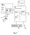
FIG. 7 , a VLSI wafer test system, in which methods according to an embodiment of the present invention are performed, is depicted. Awafer tester 50 includes aboundary scan unit 50A for providing stimulus to and retrieving data from adie 52A on a wafer undertest 52 via aprobe head 53 having electrical test connections to die52A.Wafer tester 50 includes aphase measurement unit 50C, that evaluates a phase of external clock signal generated byclock generator 50B and supplied to die52A byprobe head 53. - A
workstation computer 58, having aprocessor 56 coupled to amemory 57, for executing program instructions frommemory 57, wherein the program instructions include program instructions for receiving data fromwafer tester 50 and/or circuits withinwafer 52 in accordance with an embodiment of the present invention, is coupled towafer tester 50. Generally the methods of the present invention operatescan unit 50A to set delays dl1-dl3 and select a particular clock and edge for measurement and access the storage array values with read and write operations. The methods also measure the phase of external clock signal ext clk with respect to occurrence of the selected edge of the selected clock signal under measurement. As an alternative to usingphase measurement unit 50C, counters may be included within the die circuits to count the cycles of external clock signal ext clk, and the counter values read from scan chains viatester scan unit 50A. Program instructions obtain the counts fromwafer tester 50 or read the counts fromwafer 52, then process the counts to obtain the phase of external clock signal ext clk. The program instructions may be loaded from a storage media such as optical disc CD via a CD-ROM drive 55 or other suitable optical or magnetic/non-volatile memory drive. The data produced by embodiments of the present invention are collected from multiple tests of particular ones or all ofstorage cells 10 within dies52A, and may be performed under varying temperature and power supply voltage conditions to completely characterize the timing margins within the storage array circuit. The results of all of the measurements can then be evaluated to either change the design of the array control llgic orstorage cells 10, determine whether fabrication process has deviated exceedingly from tolerable norms or to determine operational ranges such as power supply voltage tolerances and access cycle times. - Data from delay/pulse width tests in accordance with embodiments of the invention are transferred to
workstation computer 58 viawafer tester 50 and stored inmemory 57 and/or other media storage such as a hard disk.Workstation computer 58 is also coupled to agraphical display 59 for displaying program output such as the measured edge phase and/or pulse width and delay results of the memory tests described above.Graphical display 59 may also display textual or graphical results showing timing margin resultant information and distributions of measured values.Workstation computer 58 is further coupled to input devices such as amouse 54B and akeyboard 54A for receiving user input.Workstation computer 58 may be coupled to a public network such as the Internet, or may be a private network such as the various “intra-nets” and software containing program instructions for analyzing data produced by methods and circuits in accordance with embodiments of the present invention may be located on remote computers or locally withinworkstation computer 58. Further,workstation computer 58 may be coupled towafer tester 50 by such a network connection. - While the system of
FIG. 6 depicts a configuration suitable for sequential test of a plurality of dies on a wafer, the depicted system is illustrative and not limiting to the present invention.Probe head 53 may be a multi-die full wafer probe system, or may comprise multiple probe heads for simultaneously testing multiple wafers on a single or multiple die basis. Additionally, while scan chain data retrieval and stimulus is illustrated, the techniques of the present invention may also be applied to other interfaces available to probewafer 52, or applied to circuits implemented in fully functional dies where data extraction is performed over a serial or parallel bus or other interface. - While the invention has been particularly shown and described with reference to the preferred embodiment thereof, it will be understood by those skilled in the art that the foregoing and other changes in form, and details may be made therein without departing from the spirit and scope of the invention.
Claims (25)
Priority Applications (4)
| Application Number | Priority Date | Filing Date | Title |
|---|---|---|---|
| US11/935,566US7668037B2 (en) | 2007-11-06 | 2007-11-06 | Storage array including a local clock buffer with programmable timing |
| KR1020107009256AKR101174568B1 (en) | 2007-11-06 | 2008-10-28 | Storage array including a local clock buffer with programmable timing |
| PCT/KR2008/006336WO2009061093A2 (en) | 2007-11-06 | 2008-10-28 | Storage array including a local clock buffer with programmable timing |
| JP2010532997AJP5437258B2 (en) | 2007-11-06 | 2008-10-28 | Method for measuring timing characteristics of storage circuits and storage arrays (storage arrays including local clock buffers with programmable timing) |
Applications Claiming Priority (1)
| Application Number | Priority Date | Filing Date | Title |
|---|---|---|---|
| US11/935,566US7668037B2 (en) | 2007-11-06 | 2007-11-06 | Storage array including a local clock buffer with programmable timing |
Publications (2)
| Publication Number | Publication Date |
|---|---|
| US20090116312A1true US20090116312A1 (en) | 2009-05-07 |
| US7668037B2 US7668037B2 (en) | 2010-02-23 |
Family
ID=40587959
Family Applications (1)
| Application Number | Title | Priority Date | Filing Date |
|---|---|---|---|
| US11/935,566Active2028-08-05US7668037B2 (en) | 2007-11-06 | 2007-11-06 | Storage array including a local clock buffer with programmable timing |
Country Status (4)
| Country | Link |
|---|---|
| US (1) | US7668037B2 (en) |
| JP (1) | JP5437258B2 (en) |
| KR (1) | KR101174568B1 (en) |
| WO (1) | WO2009061093A2 (en) |
Cited By (9)
| Publication number | Priority date | Publication date | Assignee | Title |
|---|---|---|---|---|
| US20090102508A1 (en)* | 2007-10-22 | 2009-04-23 | Agarwal Kanak B | Pulsed Dynamic Logic Environment Metric Measurement Circuit |
| US20090326840A1 (en)* | 2008-06-26 | 2009-12-31 | International Business Machines Corporation | Temperature-Profiled Device Fingerprint Generation and Authentication from Power-Up States of Static Cells |
| US20100213978A1 (en)* | 2009-02-20 | 2010-08-26 | Sunil Papanchand Khatri | Low power reconfigurable circuits with delay compensation |
| US20110242912A1 (en)* | 2010-04-01 | 2011-10-06 | Kang Byung-Ho | Random Access Memory Devices Having Word Line Drivers Therein That Support Variable-Frequency Clock Signals |
| US10324841B2 (en)* | 2013-07-27 | 2019-06-18 | Netlist, Inc. | Memory module with local synchronization |
| CN110679087A (en)* | 2017-06-16 | 2020-01-10 | 国际商业机器公司 | Improving resolution of on-chip timing uncertainty measurements |
| US20200082874A1 (en)* | 2018-09-11 | 2020-03-12 | Kabushiki Kaisha Toshiba | Semiconductor memory device |
| EP3757998A1 (en)* | 2013-11-26 | 2020-12-30 | Qualcomm Incorporated | Static random access memory (sram) global bitline circuits for reducing power glitches during memory read accesses, and related methods and systems |
| WO2024030197A1 (en)* | 2022-08-02 | 2024-02-08 | Apple Inc. | Multi-chain measurement circuit |
Families Citing this family (13)
| Publication number | Priority date | Publication date | Assignee | Title |
|---|---|---|---|---|
| US7760565B2 (en)* | 2007-07-24 | 2010-07-20 | International Business Machines Corporation | Wordline-to-bitline output timing ring oscillator circuit for evaluating storage array performance |
| US8345497B2 (en) | 2010-06-23 | 2013-01-01 | International Business Machines Corporation | Internal bypassing of memory array devices |
| US8345490B2 (en) | 2010-06-23 | 2013-01-01 | International Business Machines Corporation | Split voltage level restore and evaluate clock signals for memory address decoding |
| US8351278B2 (en) | 2010-06-23 | 2013-01-08 | International Business Machines Corporation | Jam latch for latching memory array output data |
| US8599642B2 (en) | 2010-06-23 | 2013-12-03 | International Business Machines Corporation | Port enable signal generation for gating a memory array device output |
| US8754691B2 (en) | 2012-09-27 | 2014-06-17 | International Business Machines Corporation | Memory array pulse width control |
| US8643168B1 (en) | 2012-10-16 | 2014-02-04 | Lattice Semiconductor Corporation | Integrated circuit package with input capacitance compensation |
| US9070433B1 (en) | 2014-03-11 | 2015-06-30 | International Business Machines Corporation | SRAM supply voltage global bitline precharge pulse |
| DE102018128927B4 (en)* | 2018-08-31 | 2024-06-27 | Taiwan Semiconductor Manufacturing Co., Ltd. | Wordline activation for variable delay |
| US10901454B2 (en) | 2019-02-06 | 2021-01-26 | Qualcomm Incorporated | Clock buffering to reduce memory hold time |
| CN112767977B (en) | 2020-12-31 | 2023-09-26 | 深圳市紫光同创电子有限公司 | Read and write window calibration circuit and method, memory, FPGA chip |
| US11456729B1 (en) | 2021-03-26 | 2022-09-27 | Analog Devices, Inc. | Deskew cell for delay and pulse width adjustment |
| US11947891B2 (en) | 2021-08-20 | 2024-04-02 | International Business Machines Corporation | Balancing cycle stealing with early mode violations |
Citations (9)
| Publication number | Priority date | Publication date | Assignee | Title |
|---|---|---|---|---|
| US4769791A (en)* | 1986-08-06 | 1988-09-06 | Advanced Micro Devices, Inc. | On-chip pulse-width control circuit for SRAM memories |
| US5122978A (en)* | 1989-09-07 | 1992-06-16 | Amdahl Corporation | Pulse width measurement technique |
| US6252820B1 (en)* | 1999-08-05 | 2001-06-26 | Kabushiki Kaisha Toshiba | Semiconductor memory device capable of monitoring and adjusting the timing and pulse width of internal control signals |
| US6414535B1 (en)* | 1995-02-06 | 2002-07-02 | Mitsubishi Denki Kabushiki Kaisha | Semiconductor device realizing internal operational factor corresponding to an external operational factor stably regardless of fluctuation of external operational factor |
| US20020152434A1 (en)* | 2001-04-12 | 2002-10-17 | International Business Machines Corporation | SOI cell stability test method |
| US6549452B1 (en)* | 2001-12-20 | 2003-04-15 | Integrated Device Technology, Inc. | Variable width wordline pulses in a memory device |
| US20040105339A1 (en)* | 2002-11-28 | 2004-06-03 | Satoshi Iwahashi | Semiconductor memory device |
| US6891772B2 (en)* | 2000-07-07 | 2005-05-10 | Mosaid Technologies Incorporated | High speed DRAM architecture with uniform access latency |
| US20050204211A1 (en)* | 2004-01-15 | 2005-09-15 | Vincent Gouin | Apparatus for determining the access time and/or the minimally allowable cycle time of a memory |
Family Cites Families (13)
| Publication number | Priority date | Publication date | Assignee | Title |
|---|---|---|---|---|
| US4603292A (en)* | 1984-04-03 | 1986-07-29 | Honeywell Information Systems Inc. | Frequency and time measurement circuit |
| JP2509275B2 (en)* | 1988-02-02 | 1996-06-19 | 富士通株式会社 | Semiconductor memory device |
| JPH03230395A (en)* | 1990-02-02 | 1991-10-14 | Hitachi Ltd | Static type ram |
| JP2606082B2 (en)* | 1993-07-02 | 1997-04-30 | 日本電気株式会社 | Semiconductor integrated circuit |
| JP2001052497A (en)* | 1999-08-05 | 2001-02-23 | Mitsubishi Electric Corp | Semiconductor memory failure information acquisition method, semiconductor memory repair analysis device, and semiconductor memory device |
| JP4301680B2 (en)* | 2000-02-29 | 2009-07-22 | 株式会社ルネサステクノロジ | Semiconductor integrated circuit device |
| JP2002042466A (en)* | 2000-07-21 | 2002-02-08 | Mitsubishi Electric Corp | Semiconductor device and semiconductor storage device |
| JP2002196053A (en) | 2000-12-25 | 2002-07-10 | Ando Electric Co Ltd | Ic measurement device |
| JP2003242799A (en)* | 2002-02-12 | 2003-08-29 | Hitachi Ltd | Semiconductor integrated circuit |
| JP2004158144A (en)* | 2002-11-07 | 2004-06-03 | Renesas Technology Corp | Semiconductor integrated circuit |
| US7236555B2 (en)* | 2004-01-23 | 2007-06-26 | Sunrise Telecom Incorporated | Method and apparatus for measuring jitter |
| US7272061B2 (en) | 2005-01-24 | 2007-09-18 | Intel Corporation | Dynamic pre-charge level control in semiconductor devices |
| WO2007099579A1 (en)* | 2006-02-28 | 2007-09-07 | Fujitsu Limited | Ram macro and timing generating circuit for same |
- 2007
- 2007-11-06USUS11/935,566patent/US7668037B2/enactiveActive
- 2008
- 2008-10-28KRKR1020107009256Apatent/KR101174568B1/ennot_activeExpired - Fee Related
- 2008-10-28JPJP2010532997Apatent/JP5437258B2/ennot_activeExpired - Fee Related
- 2008-10-28WOPCT/KR2008/006336patent/WO2009061093A2/enactiveApplication Filing
Patent Citations (9)
| Publication number | Priority date | Publication date | Assignee | Title |
|---|---|---|---|---|
| US4769791A (en)* | 1986-08-06 | 1988-09-06 | Advanced Micro Devices, Inc. | On-chip pulse-width control circuit for SRAM memories |
| US5122978A (en)* | 1989-09-07 | 1992-06-16 | Amdahl Corporation | Pulse width measurement technique |
| US6414535B1 (en)* | 1995-02-06 | 2002-07-02 | Mitsubishi Denki Kabushiki Kaisha | Semiconductor device realizing internal operational factor corresponding to an external operational factor stably regardless of fluctuation of external operational factor |
| US6252820B1 (en)* | 1999-08-05 | 2001-06-26 | Kabushiki Kaisha Toshiba | Semiconductor memory device capable of monitoring and adjusting the timing and pulse width of internal control signals |
| US6891772B2 (en)* | 2000-07-07 | 2005-05-10 | Mosaid Technologies Incorporated | High speed DRAM architecture with uniform access latency |
| US20020152434A1 (en)* | 2001-04-12 | 2002-10-17 | International Business Machines Corporation | SOI cell stability test method |
| US6549452B1 (en)* | 2001-12-20 | 2003-04-15 | Integrated Device Technology, Inc. | Variable width wordline pulses in a memory device |
| US20040105339A1 (en)* | 2002-11-28 | 2004-06-03 | Satoshi Iwahashi | Semiconductor memory device |
| US20050204211A1 (en)* | 2004-01-15 | 2005-09-15 | Vincent Gouin | Apparatus for determining the access time and/or the minimally allowable cycle time of a memory |
Cited By (18)
| Publication number | Priority date | Publication date | Assignee | Title |
|---|---|---|---|---|
| US7659749B2 (en)* | 2007-10-22 | 2010-02-09 | International Business Machines Corporation | Pulsed dynamic logic environment metric measurement circuit |
| US20090102508A1 (en)* | 2007-10-22 | 2009-04-23 | Agarwal Kanak B | Pulsed Dynamic Logic Environment Metric Measurement Circuit |
| US8219857B2 (en)* | 2008-06-26 | 2012-07-10 | International Business Machines Corporation | Temperature-profiled device fingerprint generation and authentication from power-up states of static cells |
| US20090326840A1 (en)* | 2008-06-26 | 2009-12-31 | International Business Machines Corporation | Temperature-Profiled Device Fingerprint Generation and Authentication from Power-Up States of Static Cells |
| US8880954B2 (en) | 2008-06-26 | 2014-11-04 | International Business Machines Corporation | Temperature-profiled device fingerprint generation and authentication from power-up states of static cells |
| US8495431B2 (en) | 2008-06-26 | 2013-07-23 | International Business Machines Corporation | Temperature-profiled device fingerprint generation and authentication from power-up states of static cells |
| US7880505B2 (en)* | 2009-02-20 | 2011-02-01 | Sunil Papanchand Khatri | Low power reconfigurable circuits with delay compensation |
| US20100213978A1 (en)* | 2009-02-20 | 2010-08-26 | Sunil Papanchand Khatri | Low power reconfigurable circuits with delay compensation |
| US8432755B2 (en)* | 2010-04-01 | 2013-04-30 | Samsung Electronics Co., Ltd. | Random access memory devices having word line drivers therein that support variable-frequency clock signals |
| US20110242912A1 (en)* | 2010-04-01 | 2011-10-06 | Kang Byung-Ho | Random Access Memory Devices Having Word Line Drivers Therein That Support Variable-Frequency Clock Signals |
| US8750056B2 (en) | 2010-04-01 | 2014-06-10 | Samsung Electronics Co., Ltd. | Random access memory devices having word line drivers therein that support variable-frequency clock signals |
| US10324841B2 (en)* | 2013-07-27 | 2019-06-18 | Netlist, Inc. | Memory module with local synchronization |
| US10884923B2 (en) | 2013-07-27 | 2021-01-05 | Netlist, Inc. | Memory module with local synchronization and method of operation |
| EP3757998A1 (en)* | 2013-11-26 | 2020-12-30 | Qualcomm Incorporated | Static random access memory (sram) global bitline circuits for reducing power glitches during memory read accesses, and related methods and systems |
| CN110679087A (en)* | 2017-06-16 | 2020-01-10 | 国际商业机器公司 | Improving resolution of on-chip timing uncertainty measurements |
| US20200082874A1 (en)* | 2018-09-11 | 2020-03-12 | Kabushiki Kaisha Toshiba | Semiconductor memory device |
| WO2024030197A1 (en)* | 2022-08-02 | 2024-02-08 | Apple Inc. | Multi-chain measurement circuit |
| US12204287B2 (en) | 2022-08-02 | 2025-01-21 | Apple Inc. | Multi-chain measurement circuit |
Also Published As
| Publication number | Publication date |
|---|---|
| KR20100075564A (en) | 2010-07-02 |
| US7668037B2 (en) | 2010-02-23 |
| WO2009061093A2 (en) | 2009-05-14 |
| WO2009061093A3 (en) | 2009-07-02 |
| JP2011503766A (en) | 2011-01-27 |
| KR101174568B1 (en) | 2012-08-16 |
| JP5437258B2 (en) | 2014-03-12 |
Similar Documents
| Publication | Publication Date | Title |
|---|---|---|
| US7668037B2 (en) | Storage array including a local clock buffer with programmable timing | |
| US7564739B2 (en) | Storage cell design evaluation circuit including a wordline timing and cell access detection circuit | |
| US7409305B1 (en) | Pulsed ring oscillator circuit for storage cell read timing evaluation | |
| US7376001B2 (en) | Row circuit ring oscillator method for evaluating memory cell performance | |
| US7515491B2 (en) | Method for evaluating leakage effects on static memory cell access time | |
| US7760565B2 (en) | Wordline-to-bitline output timing ring oscillator circuit for evaluating storage array performance | |
| EP0337106B1 (en) | Embedded array access time test | |
| JP5134558B2 (en) | Data processing apparatus and method for testing the stability of memory cells in a memory device | |
| US20010048623A1 (en) | Semiconductor memory device having a circuit for fast operation | |
| US7355902B2 (en) | Methods and apparatus for inline characterization of high speed operating margins of a storage element | |
| US7304895B2 (en) | Bitline variable methods and circuits for evaluating static memory cell dynamic stability | |
| Arslan et al. | Variation-tolerant SRAM sense-amplifier timing using configurable replica bitlines | |
| Kinseher et al. | Improving testability and reliability of advanced SRAM architectures | |
| US20150063010A1 (en) | Negative bias thermal instability stress testing for static random access memory (sram) | |
| Kumari et al. | FPGA implementation of memory design and testing | |
| GB2464126A (en) | Storage array including a local clock buffer with adjustable timing | |
| KR100338817B1 (en) | Refresh characteristics self tester for a memory merged logic | |
| Kumar et al. | Identification of weak bits in SRAM | |
| Narahari et al. | Modeling and Simulation Experiment on a Built-In Self Test for Memory Fault Detection in SRAM | |
| Vaghasia | Design & Characterization Of HD1P and HS1P Memory Compiler |
Legal Events
| Date | Code | Title | Description |
|---|---|---|---|
| AS | Assignment | Owner name:INTERNATIONAL BUSINESS MACHINES CORPORATION, NEW Y Free format text:ASSIGNMENT OF ASSIGNORS INTEREST;ASSIGNORS:CARPENTER, GARY D.;GEBARA, FADI H.;KAO, JERRY C.;AND OTHERS;REEL/FRAME:020073/0204;SIGNING DATES FROM 20071016 TO 20071106 Owner name:INTERNATIONAL BUSINESS MACHINES CORPORATION,NEW YO Free format text:ASSIGNMENT OF ASSIGNORS INTEREST;ASSIGNORS:CARPENTER, GARY D.;GEBARA, FADI H.;KAO, JERRY C.;AND OTHERS;SIGNING DATES FROM 20071016 TO 20071106;REEL/FRAME:020073/0204 | |
| FEPP | Fee payment procedure | Free format text:PAYOR NUMBER ASSIGNED (ORIGINAL EVENT CODE: ASPN); ENTITY STATUS OF PATENT OWNER: LARGE ENTITY | |
| STCF | Information on status: patent grant | Free format text:PATENTED CASE | |
| REMI | Maintenance fee reminder mailed | ||
| FPAY | Fee payment | Year of fee payment:4 | |
| SULP | Surcharge for late payment | ||
| AS | Assignment | Owner name:GLOBALFOUNDRIES U.S. 2 LLC, NEW YORK Free format text:ASSIGNMENT OF ASSIGNORS INTEREST;ASSIGNOR:INTERNATIONAL BUSINESS MACHINES CORPORATION;REEL/FRAME:036550/0001 Effective date:20150629 | |
| AS | Assignment | Owner name:GLOBALFOUNDRIES INC., CAYMAN ISLANDS Free format text:ASSIGNMENT OF ASSIGNORS INTEREST;ASSIGNORS:GLOBALFOUNDRIES U.S. 2 LLC;GLOBALFOUNDRIES U.S. INC.;REEL/FRAME:036779/0001 Effective date:20150910 | |
| FPAY | Fee payment | Year of fee payment:8 | |
| AS | Assignment | Owner name:WILMINGTON TRUST, NATIONAL ASSOCIATION, DELAWARE Free format text:SECURITY AGREEMENT;ASSIGNOR:GLOBALFOUNDRIES INC.;REEL/FRAME:049490/0001 Effective date:20181127 | |
| AS | Assignment | Owner name:GLOBALFOUNDRIES U.S. INC., CALIFORNIA Free format text:ASSIGNMENT OF ASSIGNORS INTEREST;ASSIGNOR:GLOBALFOUNDRIES INC.;REEL/FRAME:054633/0001 Effective date:20201022 | |
| AS | Assignment | Owner name:GLOBALFOUNDRIES INC., CAYMAN ISLANDS Free format text:RELEASE BY SECURED PARTY;ASSIGNOR:WILMINGTON TRUST, NATIONAL ASSOCIATION;REEL/FRAME:054636/0001 Effective date:20201117 | |
| AS | Assignment | Owner name:GLOBALFOUNDRIES U.S. INC., NEW YORK Free format text:RELEASE BY SECURED PARTY;ASSIGNOR:WILMINGTON TRUST, NATIONAL ASSOCIATION;REEL/FRAME:056987/0001 Effective date:20201117 | |
| MAFP | Maintenance fee payment | Free format text:PAYMENT OF MAINTENANCE FEE, 12TH YEAR, LARGE ENTITY (ORIGINAL EVENT CODE: M1553); ENTITY STATUS OF PATENT OWNER: LARGE ENTITY Year of fee payment:12 |