US20090111246A1 - Inhibitors for selective deposition of silicon containing films - Google Patents
Inhibitors for selective deposition of silicon containing filmsDownload PDFInfo
- Publication number
- US20090111246A1 US20090111246A1US11/925,518US92551807AUS2009111246A1US 20090111246 A1US20090111246 A1US 20090111246A1US 92551807 AUS92551807 AUS 92551807AUS 2009111246 A1US2009111246 A1US 2009111246A1
- Authority
- US
- United States
- Prior art keywords
- source
- silicon
- gas
- chlorine
- inhibitor
- Prior art date
- Legal status (The legal status is an assumption and is not a legal conclusion. Google has not performed a legal analysis and makes no representation as to the accuracy of the status listed.)
- Granted
Links
Images


Classifications
- C—CHEMISTRY; METALLURGY
- C30—CRYSTAL GROWTH
- C30B—SINGLE-CRYSTAL GROWTH; UNIDIRECTIONAL SOLIDIFICATION OF EUTECTIC MATERIAL OR UNIDIRECTIONAL DEMIXING OF EUTECTOID MATERIAL; REFINING BY ZONE-MELTING OF MATERIAL; PRODUCTION OF A HOMOGENEOUS POLYCRYSTALLINE MATERIAL WITH DEFINED STRUCTURE; SINGLE CRYSTALS OR HOMOGENEOUS POLYCRYSTALLINE MATERIAL WITH DEFINED STRUCTURE; AFTER-TREATMENT OF SINGLE CRYSTALS OR A HOMOGENEOUS POLYCRYSTALLINE MATERIAL WITH DEFINED STRUCTURE; APPARATUS THEREFOR
- C30B29/00—Single crystals or homogeneous polycrystalline material with defined structure characterised by the material or by their shape
- C30B29/02—Elements
- C30B29/06—Silicon
- C—CHEMISTRY; METALLURGY
- C23—COATING METALLIC MATERIAL; COATING MATERIAL WITH METALLIC MATERIAL; CHEMICAL SURFACE TREATMENT; DIFFUSION TREATMENT OF METALLIC MATERIAL; COATING BY VACUUM EVAPORATION, BY SPUTTERING, BY ION IMPLANTATION OR BY CHEMICAL VAPOUR DEPOSITION, IN GENERAL; INHIBITING CORROSION OF METALLIC MATERIAL OR INCRUSTATION IN GENERAL
- C23C—COATING METALLIC MATERIAL; COATING MATERIAL WITH METALLIC MATERIAL; SURFACE TREATMENT OF METALLIC MATERIAL BY DIFFUSION INTO THE SURFACE, BY CHEMICAL CONVERSION OR SUBSTITUTION; COATING BY VACUUM EVAPORATION, BY SPUTTERING, BY ION IMPLANTATION OR BY CHEMICAL VAPOUR DEPOSITION, IN GENERAL
- C23C16/00—Chemical coating by decomposition of gaseous compounds, without leaving reaction products of surface material in the coating, i.e. chemical vapour deposition [CVD] processes
- C23C16/04—Coating on selected surface areas, e.g. using masks
- C—CHEMISTRY; METALLURGY
- C23—COATING METALLIC MATERIAL; COATING MATERIAL WITH METALLIC MATERIAL; CHEMICAL SURFACE TREATMENT; DIFFUSION TREATMENT OF METALLIC MATERIAL; COATING BY VACUUM EVAPORATION, BY SPUTTERING, BY ION IMPLANTATION OR BY CHEMICAL VAPOUR DEPOSITION, IN GENERAL; INHIBITING CORROSION OF METALLIC MATERIAL OR INCRUSTATION IN GENERAL
- C23C—COATING METALLIC MATERIAL; COATING MATERIAL WITH METALLIC MATERIAL; SURFACE TREATMENT OF METALLIC MATERIAL BY DIFFUSION INTO THE SURFACE, BY CHEMICAL CONVERSION OR SUBSTITUTION; COATING BY VACUUM EVAPORATION, BY SPUTTERING, BY ION IMPLANTATION OR BY CHEMICAL VAPOUR DEPOSITION, IN GENERAL
- C23C16/00—Chemical coating by decomposition of gaseous compounds, without leaving reaction products of surface material in the coating, i.e. chemical vapour deposition [CVD] processes
- C23C16/44—Chemical coating by decomposition of gaseous compounds, without leaving reaction products of surface material in the coating, i.e. chemical vapour deposition [CVD] processes characterised by the method of coating
- C23C16/455—Chemical coating by decomposition of gaseous compounds, without leaving reaction products of surface material in the coating, i.e. chemical vapour deposition [CVD] processes characterised by the method of coating characterised by the method used for introducing gases into reaction chamber or for modifying gas flows in reaction chamber
- C23C16/45512—Premixing before introduction in the reaction chamber
- C—CHEMISTRY; METALLURGY
- C23—COATING METALLIC MATERIAL; COATING MATERIAL WITH METALLIC MATERIAL; CHEMICAL SURFACE TREATMENT; DIFFUSION TREATMENT OF METALLIC MATERIAL; COATING BY VACUUM EVAPORATION, BY SPUTTERING, BY ION IMPLANTATION OR BY CHEMICAL VAPOUR DEPOSITION, IN GENERAL; INHIBITING CORROSION OF METALLIC MATERIAL OR INCRUSTATION IN GENERAL
- C23C—COATING METALLIC MATERIAL; COATING MATERIAL WITH METALLIC MATERIAL; SURFACE TREATMENT OF METALLIC MATERIAL BY DIFFUSION INTO THE SURFACE, BY CHEMICAL CONVERSION OR SUBSTITUTION; COATING BY VACUUM EVAPORATION, BY SPUTTERING, BY ION IMPLANTATION OR BY CHEMICAL VAPOUR DEPOSITION, IN GENERAL
- C23C16/00—Chemical coating by decomposition of gaseous compounds, without leaving reaction products of surface material in the coating, i.e. chemical vapour deposition [CVD] processes
- C23C16/44—Chemical coating by decomposition of gaseous compounds, without leaving reaction products of surface material in the coating, i.e. chemical vapour deposition [CVD] processes characterised by the method of coating
- C23C16/455—Chemical coating by decomposition of gaseous compounds, without leaving reaction products of surface material in the coating, i.e. chemical vapour deposition [CVD] processes characterised by the method of coating characterised by the method used for introducing gases into reaction chamber or for modifying gas flows in reaction chamber
- C23C16/45561—Gas plumbing upstream of the reaction chamber
- C—CHEMISTRY; METALLURGY
- C30—CRYSTAL GROWTH
- C30B—SINGLE-CRYSTAL GROWTH; UNIDIRECTIONAL SOLIDIFICATION OF EUTECTIC MATERIAL OR UNIDIRECTIONAL DEMIXING OF EUTECTOID MATERIAL; REFINING BY ZONE-MELTING OF MATERIAL; PRODUCTION OF A HOMOGENEOUS POLYCRYSTALLINE MATERIAL WITH DEFINED STRUCTURE; SINGLE CRYSTALS OR HOMOGENEOUS POLYCRYSTALLINE MATERIAL WITH DEFINED STRUCTURE; AFTER-TREATMENT OF SINGLE CRYSTALS OR A HOMOGENEOUS POLYCRYSTALLINE MATERIAL WITH DEFINED STRUCTURE; APPARATUS THEREFOR
- C30B25/00—Single-crystal growth by chemical reaction of reactive gases, e.g. chemical vapour-deposition growth
- C30B25/02—Epitaxial-layer growth
- H—ELECTRICITY
- H01—ELECTRIC ELEMENTS
- H01L—SEMICONDUCTOR DEVICES NOT COVERED BY CLASS H10
- H01L21/00—Processes or apparatus adapted for the manufacture or treatment of semiconductor or solid state devices or of parts thereof
- H01L21/02—Manufacture or treatment of semiconductor devices or of parts thereof
- H01L21/02104—Forming layers
- H01L21/02365—Forming inorganic semiconducting materials on a substrate
- H01L21/02518—Deposited layers
- H01L21/02521—Materials
- H01L21/02524—Group 14 semiconducting materials
- H01L21/02529—Silicon carbide
- H—ELECTRICITY
- H01—ELECTRIC ELEMENTS
- H01L—SEMICONDUCTOR DEVICES NOT COVERED BY CLASS H10
- H01L21/00—Processes or apparatus adapted for the manufacture or treatment of semiconductor or solid state devices or of parts thereof
- H01L21/02—Manufacture or treatment of semiconductor devices or of parts thereof
- H01L21/02104—Forming layers
- H01L21/02365—Forming inorganic semiconducting materials on a substrate
- H01L21/02518—Deposited layers
- H01L21/02521—Materials
- H01L21/02524—Group 14 semiconducting materials
- H01L21/02532—Silicon, silicon germanium, germanium
- H—ELECTRICITY
- H01—ELECTRIC ELEMENTS
- H01L—SEMICONDUCTOR DEVICES NOT COVERED BY CLASS H10
- H01L21/00—Processes or apparatus adapted for the manufacture or treatment of semiconductor or solid state devices or of parts thereof
- H01L21/02—Manufacture or treatment of semiconductor devices or of parts thereof
- H01L21/02104—Forming layers
- H01L21/02365—Forming inorganic semiconducting materials on a substrate
- H01L21/02518—Deposited layers
- H01L21/02521—Materials
- H01L21/02524—Group 14 semiconducting materials
- H01L21/02535—Group 14 semiconducting materials including tin
- H—ELECTRICITY
- H01—ELECTRIC ELEMENTS
- H01L—SEMICONDUCTOR DEVICES NOT COVERED BY CLASS H10
- H01L21/00—Processes or apparatus adapted for the manufacture or treatment of semiconductor or solid state devices or of parts thereof
- H01L21/02—Manufacture or treatment of semiconductor devices or of parts thereof
- H01L21/02104—Forming layers
- H01L21/02365—Forming inorganic semiconducting materials on a substrate
- H01L21/02518—Deposited layers
- H01L21/0257—Doping during depositing
- H01L21/02573—Conductivity type
- H—ELECTRICITY
- H01—ELECTRIC ELEMENTS
- H01L—SEMICONDUCTOR DEVICES NOT COVERED BY CLASS H10
- H01L21/00—Processes or apparatus adapted for the manufacture or treatment of semiconductor or solid state devices or of parts thereof
- H01L21/02—Manufacture or treatment of semiconductor devices or of parts thereof
- H01L21/02104—Forming layers
- H01L21/02365—Forming inorganic semiconducting materials on a substrate
- H01L21/02612—Formation types
- H01L21/02617—Deposition types
- H01L21/0262—Reduction or decomposition of gaseous compounds, e.g. CVD
- H—ELECTRICITY
- H01—ELECTRIC ELEMENTS
- H01L—SEMICONDUCTOR DEVICES NOT COVERED BY CLASS H10
- H01L21/00—Processes or apparatus adapted for the manufacture or treatment of semiconductor or solid state devices or of parts thereof
- H01L21/02—Manufacture or treatment of semiconductor devices or of parts thereof
- H01L21/02104—Forming layers
- H01L21/02365—Forming inorganic semiconducting materials on a substrate
- H01L21/02612—Formation types
- H01L21/02617—Deposition types
- H01L21/02636—Selective deposition, e.g. simultaneous growth of mono- and non-monocrystalline semiconductor materials
Definitions
- This applicationrelates generally to the deposition of silicon-containing materials in semiconductor processing. More particularly, this application relates to the selective deposition of silicon-containing films.
- heterojunction bipolar transistorsare often fabricated using selective deposition techniques that deposit epitaxially-deposited single-crystal, e.g., semiconductor films only on active areas.
- Other transistor designsbenefit from elevated source/drain structures, which provide additional silicon that can be consumed by the source/drain contact process without altering shallow junction device performance.
- Selective epitaxy on source/drain regionsadvantageously reduces the need for subsequent patterning and etch steps.
- selective depositiontakes advantage of differential nucleation during deposition on disparate materials. The precursor of choice will generally have a tendency to nucleate and grow more rapidly on one surface and less rapidly on another surface.
- discontinuous films on oxidehave a high exposed surface area relative to merged, continuous films on silicon. Accordingly, an etchant added to the process will have a greater effect upon the poorly nucleating film on the oxide as compared to the rapidly nucleating film on the silicon.
- the relative selectivity of a processcan thus be tuned by adjusting factors that affect the deposition rate, such as precursor flow rates, temperature, pressure and the rate of etching, such as etchant flow rate, temperature, pressure. Changes in each variable will generally have different effects upon etch rate and deposition rate.
- a selective deposition processis tuned to produce the highest deposition rate feasible on the window of interest while accomplishing no deposition in the field regions.
- An embodimentprovides a method for depositing a single crystalline silicon film.
- the methodincludes providing a substrate disposed within a chamber.
- a silicon precursoris introduced to the chamber under chemical vapor deposition conditions.
- a chlorine-containing etchantis introduced to the chamber.
- An inhibitor sourceis introduced for decelerating reactions between the silicon precursor and the chlorine-containing etchant.
- a crystalline Si-containing filmis selectively deposited onto the substrate.
- Another embodimentprovides a method of depositing a crystalline Si-containing film.
- the methodincludes providing a substrate disposed within a chamber. A silicon precursor and a chlorine gas are intermixed in the chamber. Exothermic reactions between the silicon precursor and the chlorine gas are decelerated by intermixing a carbon-containing inhibitor source in the chamber. A single crystalline Si-containing film is selectively deposited onto the substrate.
- the apparatusincludes a silicon vapor source, a chlorine-containing etchant gas source and a carrier gas source.
- the apparatusalso includes an inhibitor vapor source selected from the group consisting of propylene, butadiene, benzene, napthalene, phenanthrene, anthracene, cycloheptatriene cation, cycloheptatriene, furan, pyridine, pyrrole and thiophene.
- the apparatusalso includes a gas distribution network connecting the silicon vapor, chlorine-containing etchant gas, carrier gas and inhibitor vapor sources to a chemical vapor deposition chamber.
- the apparatusalso includes a control system configured to deliver silicon vapor, chlorine-containing etchant gas, carrier gas and inhibitor vapor to the gas distribution network under conditions suited to selectively deposit a silicon-containing layer on portions of a substrate within the chamber without depositing on other portions of the substrate.
- FIG. 1is a schematic cross section of a semiconductor substrate after field oxide definition, leaving insulator and semiconductor surfaces exposed.
- FIG. 2shows the structure of FIG. 1 after formation of a transistor gate electrode within an active area window.
- FIG. 3shows the structure of FIG. 2 after recessing source and drain regions on either side of the gate electrode.
- FIG. 4shows the structure of FIG. 3 after selective deposition of a semiconductor film within the recessed regions, in accordance with a preferred embodiment.
- FIG. 5shows the structure of FIG. 4 after optional continued selective deposition, forming elevated source/drain structures.
- FIG. 6shows the structure of FIG. 2 after exposing the semiconductor window and conducting a selective deposition to form elevated source/drain structures, in accordance with another preferred embodiment.
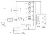
- FIG. 7is a schematic view of a reactor set up for a system employing trisilane, a chlorine-containing etchant gas, an inhibitor source and a carrier gas for selectively depositing silicon-containing films in accordance with a preferred embodiment.
- Si-containing materialand similar terms are used herein to refer to a broad variety of silicon-containing materials including without limitation Si, Si:C, SiGe, SiGe:C, Si:Sn, (Ge:Sn, Sn:C), SiGe:Sn, SiSn:C and SiGe:Sn:C.
- carbon-doped Si“Si:C,” “SiGe,” “carbon-doped SiGe,” “SiGe:C” and similar terms refer to materials that contain the indicated chemical elements in various proportions and, optionally, minor amounts of other elements.
- SiGeis a material that comprises silicon, germanium tin and carbon, and optionally, other elements, such as Group III (B, Ga) and V (P, As, Sb) dopants.
- Group III (B, Ga) and V (P, As, Sb) dopantsmay be referred to herein as Si:C or vice versa.
- Terms such as “Si:C,” “SiGe,” and “SiGe:C”are not stoichiometric chemical formulas per se and thus are not limited to materials that contain particular ratios of the indicated elements.
- the percentage of a dopant such as carbon, germanium, phosphorous, arsenic or boron in a Si-containing filmis expressed herein in atomic percent on a whole film basis, unless otherwise stated.
- the amount of germanium, tin and/or carbon substitutionally incorporated into a Si-containing materialmay be determined by measuring the perpendicular lattice spacing of the doped Si-containing material by x-ray diffraction, then applying interpolation between single crystal Si and diamond (single crystal carbon), in a manner known to those skilled in the art [Salvador Kelieres, Bertil]. Those skilled in the art are aware of the relationships between substitutional doping levels, lattice spacing and strain. See, e.g., Judy L.
- Substraterefers either to the workpiece upon which deposition is desired, or the surface exposed to the deposition gas(es).
- the substratemay be a single crystal silicon wafer, or may be a semiconductor-on-insulator (“SOI”) substrate, or may be an epitaxial Si, SiGe, Ge, GeSn or III-V material deposited upon such wafers.
- Workpiecesare not limited to wafers, but also include glass, plastic, or any other substrate employed in semiconductor processing.
- a mixed or patterned substrateis a substrate that has two or more different types of surfaces.
- a mixed substratemay comprise a first surface having a first surface morphology and a second surface having a second surface morphology.
- doped Si-containing layersare selectively formed over single crystal semiconductor materials while minimizing and more preferably avoiding deposition over adjacent dielectrics.
- dielectric materialsinclude silicon dioxide, silicon nitride, metal oxide and metal silicate.
- epitaxial, epitaxially, heteroepitaxial, “heteroepitaxially” and similar termsare used herein to refer to the deposition of a crystalline Si-containing material onto a crystalline substrate in such a way that the deposited layer adopts or follows the lattice constant of the substrate. Epitaxial deposition is homoepitaxial when the composition of the deposited layer is the same as that of the surface on which it is deposited. Epitaxial deposition is heteroepitaxial when the composition of the deposited layer is different from that of the surface on which it is deposited.
- Such a mixed substratecomprises a first surface having a first surface morphology and a second surface having a second surface morphology.
- surface morphologyrefers to the crystalline structure of the substrate surface.
- Amorphous and crystallineare examples of different morphologies.
- Polycrystalline morphologyis a crystalline structure that consists of a disorderly arrangement of orderly crystals and thus has an intermediate degree of order.
- Single crystal morphologyis a crystalline structure that has a high degree of long range order on an atomic scale.
- Epitaxial filmsare characterized by a crystal structure and orientation that is identical to the substrate upon which they are grown, typically single crystal.
- the atoms in these materialsare arranged in a lattice-like structure that persists over relatively long distances on an atomic scale.
- Amorphous morphologyis a non-crystalline structure having a low degree of order because the atoms lack a definite periodic arrangement. Other morphologies include microcrystalline and mixtures of amorphous and crystalline material.
- single-crystalis used to describe a predominantly large crystal structure that may have a tolerable number of faults therein, as is commonly employed for transistor fabrication.
- crystallinity of a layergenerally falls along a continuum from amorphous to polycrystalline to single-crystal; the skilled artisan can readily determine when a crystal structure can be considered single-crystal, despite low density faults.
- Specific examples of mixed substratesinclude without limitation single crystal/polycrystalline, single crystal/amorphous, single crystal/dielectric, conductor/dielectric, and semiconductor/dielectric.
- a low temperaturee.g., ideally about 500°-600° C.
- high growth ratee.g., at least about 5 nm/min, preferably at least about 10 nm/min
- selective growth of intrinsic silicontypically occurs at high temperatures, such as about 800°-850° C.
- conventional precursors used for the selective epitaxial growth of siliconsuch as dichlorosilane or silane, typically give very low growth rates at lower temperatures, with the growth rate dropping by a factor of about 2 every 200°C.
- precursors that decompose much more easily at low temperaturesincluding silicon hydrides such as SiH 4 , Si 2 H 6 , or Si 3 H 8 , tend to form silicon nuclei on the insulator, which also leads to non-selective growth.
- a silicon etchantis typically added to the deposition reactants.
- HClis used as an etchant to enhance selectivity
- the surfacecan become Cl-terminated at temperatures of about 750° C. or below.
- the Cl-terminated surfacecan lead to low growth rate due to the saturation of reactive sites.
- it is desirable to employ etchants more reactive than HCl for low temperature depositionsuch as at temperatures suited for high substitutional incorporation of carbon, e.g., below about 650° C.
- Cl 2can be more effective as an etching source because of its high etch efficiency in dissolving and etching silicon nuclei.
- other low temperature and aggressive etchants, and particularly chlorine-based etchantssuch as Cl 2 , may be used.
- the stable molecule SiCl 4can also be formed in the following exothermic reaction:
- Embodiments of the inventionprovide methods for selectively depositing Si-containing materials using a silicon source, an etchant, an inhibitor source and, optionally, source(s) of other elements such as electrical active dopant(s), carbon, germanium, and/or tin are used or added.
- a silicon sourcean etchant, an inhibitor source and, optionally, source(s) of other elements such as electrical active dopant(s), carbon, germanium, and/or tin are used or added.
- the delivery of the silicon source, etchant and inhibitor source to the surface of a substratepreferably results in the formation of a Si-containing film selectively over single crystal substrates or single crystal regions of mixed substrates.
- the addition of the inhibitordecelerates or suppresses exothermic reactions with the etchant to maintain high deposition rates and selectivity at low deposition temperatures.
- a polymerization reactiontypically includes chain origination, chain branching or propagation, and chain termination.
- Chain branchingis a process in which a reactive intermediary is continuously regenerated during the course of a chemical reaction.
- chain branchingoccurs when the reactive end-groups of a polymer chain react in each propagation step with a new monomer molecule, transferring the reactive group to that unit.
- Chain terminationoccurs when any chemical reaction leads to the destruction of a reactive intermediary in a chain propagation step in the course of a polymerization reaction, effectively bringing the reaction to a halt.
- the above reactionscan cause additional chain branching reactions from the subsequently formed reactive intermediaries, produce additional HCl, or increase the amount of heat emission from highly exothermic reactions, such as from the formation of SiCl 4 and other stable molecules.
- Enhancing chain termination reactionscan decelerate or suppress the above reactions, and delay or prevent self-ignition of the gas mixtures.
- One rapid chain termination reaction with a silylene radicalincludes the following reaction:
- alkene or olefin moleculessuch as propylene (C 3 H 6 )
- silylenessuch as SiH 2 , SiHCl and SiCl 2
- the rate constants of the reaction between silylenes and C 3 H 6vary from about 10 ⁇ 10 cm 3 s ⁇ 1 (for SiH 2 ) to about 10 ⁇ 11 cm 3 s ⁇ 1 (for SiHCl and SiCl 2 ).
- the heat emission of exothermic silicon-chlorine reactionscan be considerably decreased with the addition of olefin molecules since they react rapidly with silylenes, and consequently accelerate and increase the termination of some of the chain branching caused by silylene radicals as chain carriers. Accordingly, the self-ignition and excessive heat emission for silicon-chlorine reactions can be controllably decreased by adding inhibitor molecules to the silicon-chlorine mixtures for decelerating reactions between a silicon precursor and a chlorine-containing etchant, according to embodiments of the invention.
- butadiene (C 4 H 6 ) moleculesare added to the feed gas along with a silicon source and a chlorine-containing etchant.
- Butadienecan stabilize silylene radicals such as :Si 2 H 4 in the gas phase by bonding to the reactive intermediary by weak bonding forces, such as hydrogen and Van der Waals bonding, or strong bonding forces, such as donor-acceptor, covalent bonding, etc.
- inhibitor molecules that can bond to chain carriers such as silylene radicals and that can be added to the feed gas along with a silicon source and a chlorine-containing etchantinclude but are not limited to: conjugated systems, such as compounds containing one or more sequences of alternating single and multiple, including double or triple, bonds, such as carbon-carbon or carbon-oxygen bonds.
- Inhibitor moleculesinclude aromatic hydrocarbons, such as benzene, napthalene, phenanthrene, and anthracene; non-benzenoid aromatic compounds such as cycloheptatriene and aromatic annulenes; and other linear or cyclic aromatic compounds, such as furan, pyridine, pyrrole (nitrogen-containing compounds) and thiophene (sulfur-containing compound).
- aromatic hydrocarbonssuch as benzene, napthalene, phenanthrene, and anthracene
- non-benzenoid aromatic compoundssuch as cycloheptatriene and aromatic annulenes
- other linear or cyclic aromatic compoundssuch as furan, pyridine, pyrrole (nitrogen-containing compounds) and thiophene (sulfur-containing compound).
- Conjugated systemsinclude molecular structures that comprise alternating single and multiple bonds, such as CH 2 ⁇ CH—CH ⁇ CH 2 , CH 2 ⁇ CH—C ⁇ N. In such systems, conjugation is the interaction of one p-orbital with another across an intervening ⁇ -bond in such structures, although in other molecular entities, d-orbitals may be involved. Conjugated systems also include the analogous interaction of an element having a p-orbital with an unshared electron pair, e.g. :Cl—CH ⁇ CH 2 . Conjugated systems also include polyenes, which are acyclic hydrocarbons having a molecular structure containing alternating carbon-carbon double and single bonds.
- the most widely used method for determining aromaticityis the observation of diatropicity in the 1 H NMR spectrum.
- the terms ‘aromatic’ and ‘antiaromatic’have been extended to describe the stabilization or destabilization of transition states of pericyclic reactions.
- inhibitor moleculesnonetheless enhance the efficiency of deposition even if they only inhibit chain propagation in the gas phase prior to decomposing on the depositing surface. Even if the exothermic reactions with silylene radicals as described herein are not completely suppressed, the addition of inhibitor molecules can cause sufficient deceleration of the excessive heat emission and self-ignition that would occur in the absence of the inhibitors. Moreover, a small temperature increase may not in itself be harmful, and may even be beneficial for achieving high growth rates, particularly in a cold wall, quartz chamber.
- the highly exothermic reaction of, for example, trisilane in the reaction Si 3 H 8 +10Cl 2 ⁇ 3SiCl 4 +8Cl at low temperatures during the selective deposition of silicon-containing materialscan be decelerated according to embodiments of the invention.
- Other less exothermic but significant reactions with Si 2 H 6 , SiH 4 , dichlorosilane (DCS), partially chlorinated disilanes and other silicon precursorscan likewise be decelerated.
- the silicon precursor and etchant source chemicalsare at least as reactive, or produce at least as exothermic reactions, as mixtures containing dichlorosilane and chlorine gas (Cl 2 ).
- an embodimentprovides a method for depositing a single crystalline silicon film, comprising: providing a substrate disposed within a chamber; introducing to the chamber under chemical vapor deposition conditions a silicon precursor, a chlorine-containing etchant and an inhibitor source for decelerating reactions between the silicon precursor and the chlorine-containing etchant; and selectively depositing a doped crystalline Si-containing film onto the substrate.
- the inhibitoris preferably a carbon-containing molecule, such as propylene, butadiene or benzene.
- the silicon sourceis disilane, trisilane, tetrasilane, cyclopentasilane, neopentasilane, monochlorodisilane or dichlorodisilane and the chlorine-containing etchant is chlorine gas.
- the Si-containing filmis selectively formed over a single crystal semiconductor surface while minimizing or avoiding deposition over a dielectric surface in a ratio of preferably about>10:1.
- the ratio of selective depositionis about>50:1.
- the ratio of selective depositionis about 100% such that no deposition occurs on the dielectric surface at all.
- Depositionmay be suitably conducted according to the various CVD methods known to those skilled in the art, but an exemplary deposition process is conducted according to the CVD methods taught herein.
- the disclosed methodsmay be suitably practiced by employing CVD, including plasma-enhanced chemical vapor deposition (“PECVD”) or thermal CVD, utilizing a silicon source, a chlorine-containing etchant and an inhibitor source to selectively deposit a single crystalline Si-containing film onto a substrate within a CVD chamber.
- the Si-containing filmis a carbon-doped epitaxial Si film.
- referencemay be made to the use of a silicon source, a chlorine-containing etchant and an inhibitor source to deposit a Si or Si-containing film.
- Si-containing filmse.g., the deposition of SiGe:C, Si:Sn, SiGe:Sn, Ge:Sn, SiSn:C, SiGe:Sn:C or Ge:Sn:C films or films involving the use of a germanium source and/or a tin source to the deposition of electrically doped Si:C, SiGe:C, Si:Sn, SiGe:Sn, Ge:Sn, SiSn:C, SiGe:Sn:C or Ge:Sn:C films or films involving the use of a dopant precursor for an electrical dopant, unless otherwise stated.
- Thermal CVDis preferred, as deposition can be achieved effectively without the risk of damage to substrates and equipment that can occur with plasma processing.
- a silicon source, a chlorine-containing etchant, an inhibitor source, and optionally an electrical dopant precursorare introduced to the chamber in the form of separate gases or by intermixing to form a feed gas.
- the intermixing to form the feed gasmay take place within the chamber or upstream of the chamber prior to introduction of the feed gas to the chamber.
- the silicon source, chlorine-containing etchant and inhibitor sourceare introduced to the chamber in separate gases in order to minimize the harmful effects of self-ignition of the gas mixtures, such as preventing those that could occur at the gas panel. Intermixing to form a feed gas can take place in the chamber upstream of the substrate.
- the total pressure in the CVD chamberis in the range of about 0.001 Torr to about 1000 Torr. According to another embodiment, the total pressure in the CVD chamber is in the range of about 0.1 Torr to about 350 Torr. According to another embodiment, the total pressure in the CVD chamber is in the range of about 0.25 Torr to about 200 Torr. This latter range of 0.25 Torr to 200 Torr is sometimes referred to as “reduced pressure” CVD (“RPCVD”) as distinct from even lower pressure ranges for “low pressure” CVD (“LPCVD”), which are conducted in the milliTorr range. RPCVD and atmospheric CVD carry even higher risk of damaging exothermic and potentially explosive reactions.
- the chamber pressuremay be referred to herein as a deposition pressure.
- the feed gascan also include a gas or gases other than the silicon, chlorine-containing etchant and inhibitor source, such as other silicon sources, germanium sources, tin sources, etchant sources, dopant precursor(s) and/or inert carrier gases.
- a gas or gases other than the siliconchlorine-containing etchant and inhibitor source, such as other silicon sources, germanium sources, tin sources, etchant sources, dopant precursor(s) and/or inert carrier gases.
- dopant precursor(s)is used herein to refer in a general way to various materials that are precursors to various elements, such as boron, gallium, indium, arsenic, phosphorous, and/or antimony, which may be incorporated into the resulting deposited film in relatively minor amounts. It will be recognized that silicon sources may also be considered dopant precursors for the deposition of SiGe, Si:Sn or SiGe:Sn films that contain relatively minor amounts of silicon.
- the silicon sourceif liquid under storage conditions, can be introduced to the chamber by way of a vaporizer such as a bubbler used with a carrier gas to entrain the silicon source vapor.
- a gas concentration sensorcan measure the amount of the silicon source in the carrier gas flowing from the bubbler.
- Such sensorsare commercially available, e.g., Piezocon® gas concentration sensors from Lorex Industries, Poughkeepsie, N.Y., USA.
- suitable carrier gases for the methods described hereininclude He, Ar, H 2 , and N 2 . It should be understood by one skilled in the art that other suitable carrier gases may be used. However, preferably the main carrier gas, representing the largest source of gas in the system, is a non-hydrogen carrier such as He, Ar and/or N 2 . Hydrogen gas (H 2 ) is most commonly used as a carrier gas in vapor deposition for semiconductor processing, and particularly in epitaxial deposition. There are several reasons for the popularity of H 2 H 2 can be provided with a high degree of purity, and the thermal properties of hydrogen are such that it does not have as great a thermal effect on the wafer.
- a non-hydrogen carrier gasin gas mixtures for selective deposition of silicon, particular in the combination of trisilane/chlorine deposition with a substitutional dopant precursor.
- a substitutional dopant precursorPreferably helium (He), argon (Ar), neon (Ne), xenon (Xe) or nitrogen gas (N 2 ), or a combination of such inert gases, is employed in place of hydrogen.
- Heis employed, as it has thermal behavior close to that of H 2 and thus entails less tuning of the reactor for the adjustment from use of H 2 carrier gas.
- the silicon precursor and supplemental silicon sourcesmay include: silane, disilane, trisilane, tetrasilane, cyclopentasilane, neopentasilane, monochlorosilane, dichlorosilane, monochlorodisilane as silicon sources.
- the feed gasmay also contain other materials known by those skilled in the art to be useful for doping or alloying Si-containing films, as desired, such as a supplemental silicon source, germanium source, tin source, boron source, gallium source, indium source, arsenic source, phosphorous source, and/or antimony source.
- germane, and digermane and trigermaneas germanium sources
- various dopant precursorsas sources of electrical dopants (both n-type and p-type) such as antimony, arsenic, boron, gallium, indium and phosphorous.
- a suitable manifoldmay be used to supply feed gas(es) to the CVD chamber.
- the CVD chamberis preferably in a single wafer reactor, e.g., a single wafer, horizontal gas flow CVD chamber. Most preferably, the CVD chamber is in a single-wafer, single pass, laminar horizontal gas flow reactor, preferably radiantly heated.
- Suitable reactors of this typeare commercially available, and preferred models include the EpsilonTM series of single wafer reactors commercially available from ASM America, Inc. of Phoenix, Ariz.
- CVDmay be conducted by introducing plasma products in situ, or downstream of a remote plasma generator, to the chamber, but as noted above, thermal CVD is preferred.
- Thermal CVDis preferably conducted at a substrate temperature that is effective to deposit a crystalline Si-containing film over the substrate.
- thermal CVDis conducted at a temperature less than about 750° C.
- thermal CVDis conducted at a temperature less than about 650° C.
- thermal CVDis conducted at a temperature in a range of about 500-600° C.
- thermal CVDis most preferably conducted at a temperature in the range of 500-600° C.
- PECVDis preferably conducted at a temperature in the range of about 300° C. to about 700° C.
- the substratecan be heated by a variety of methods known in the art, e.g., resistive heating and lamp heating.
- an inhibitor source for decelerating exothermic reactions between a silicon precursor and chlorine-containing etchantcontains carbon-containing molecules including but not limited to, for example, propylene, butadiene, benzene, napthalene, phenanthrene, anthracene, cycloheptatriene cation, cycloheptatriene, furan, pyridine, pyrrole and thiophene.
- the carbon-containing inhibitor sourceis the source for carbon incorporation in the Si-containing film.
- the single crystalline Si-containing filmsmay be substitutionally doped with carbon, e.g., where the dopants replace Si in the lattice structure.
- the inhibitor sourceis the only source for substitutional carbon in the Si-containing film.
- supplemental carbon sourcesmay be used in addition to the inhibitor source to provide for substitutional doping of carbon.
- the lattice constant for single crystal siliconis about 5.431 ⁇
- single crystal carbon in the form of diamondhas a lattice constant of 3.567 ⁇ due to the small size of the carbon atoms. Accordingly, tensile strain may be introduced into single crystalline silicon by substitutional doping with carbon, because carbon atoms are smaller than the silicon atoms that they replace.
- the thickness of a single crystalline silicon film comprising a strain-modifying amount of substitutional carbon as described hereinis preferably less than a critical film thickness.
- a critical film thicknessis a film thickness at which a strained film relaxes under a particular set of conditions. As the concentration of substitutional dopant (e.g. carbon) increases, the critical thickness generally decreases. Films having a thickness less than the critical thickness typically remain strained under those conditions.
- a single crystalline silicon film comprising about 1.8 atomic % substitutional carbonmay have a critical thickness of about 200 mn at 550° C.
- an otherwise similar film comprising 3.5 atomic % substitutional carbonmay have a critical thickness of about 15-20 mn at the same temperature.
- Films having a thickness that is less than a critical thickness for that filmwill tend to remain strained unless or until sufficiently perturbed, or exposed to sufficient heat to cause relaxation.
- a Si:C, SiGe, SiGe:C, Si:Sn or Ge:Sn filmis configured to exert a strain on an adjacent layer. For example, a tensile strain may be exerted on a Ge film that is deposited onto a relaxed Ge:Sn layer.
- a compressive strainmay be exerted on a Ge:Sn film that is deposited onto a relaxed Ge layer.
- a strained Si:C film that is selectively formed in a recessed source/drain regionexerts a tensile strain on a silicon channel formed between the source and drain, as described in greater detail below.
- Such configurationsmay be used in various applications, e.g., to improve electron mobility for NMOS devices.
- a strained SiGe film that is selectively formed in a recessed source/drain regionexerts a tensile strain on a germanium channel formed between the source and drain.
- Such configurationsmay also be used to improve electron mobility for NMOS devices.
- a strained Ge:Sn filmthat is selectively formed in a recessed source/drain region exerts a compressive strain on a germanium channel formed between the source and drain.
- Such configurationsmay be used in various applications, e.g., to improve hole mobility for PMOS devices.
- the single crystalline Si-containing filmsmay further comprise an electrically active dopant, e.g., a dopant selected from the group consisting of phosphorous and arsenic for NMOS applications.
- an electrically active dopante.g., a dopant selected from the group consisting of phosphorous and arsenic for NMOS applications.
- Incorporation of electrically active dopants into Si-containing films by CVDis preferably accomplished by in-situ doping using dopant sources or dopant precursors.
- Preferred precursors for electrical dopantsare dopant hydrides, including p-type dopant precursors such as diborane, deuterated diborane, and n-type dopant precursors such as phosphine, arsenic vapor, and arsine.
- Silylphosphinese.g., (H 3 Si) 3-x PR x
- SbH 3 and trimethylindiumare alternative sources of antimony and indium, respectively.
- Such dopant precursorsare useful for the preparation of preferred films as described below, preferably boron-, phosphorous-, antimony-, indium-, and arsenic-doped silicon, Si:C, SiGe, SiGeC, SiGe:Sn:C, SiGe:Sn, Si:Sn:C, SiSn and Ge:Sn films and alloys.
- the amount of dopant precursor in the feed gasmay be adjusted to provide the desired level of dopant in the Si-containing film.
- Preferred concentrations of dopant precursor in the feed gasare in the range of about 1 part per billion “ppb” to about 20% by weight based on the total weight of reactive gas, excluding inert carrier and diluent gases.
- concentrations in the feed gascan be in the range of about 1 standard cubic centimeters per minute “sccm” up to about 100 sccm, although higher or lower amounts are sometimes preferred in order to achieve the desired property in the resulting film.
- concentrations of dopant precursor, such as pure phosphine or equivalent diluted phosphine, arsine or diborane, in the feed gascan be between about 0.1 sccm to about 5 sccm, although higher or lower amounts are sometimes preferred in order to achieve the desired property in the resulting film.
- dilute mixtures of the dopant precursor in a carrier gascan be delivered to the reactor via a mass flow controller with set points ranging from about 3 sccm to about 1000 sccm, depending on desired dopant concentration and dopant gas concentration. Dilution of dopant gases can lead to factors of 10 ⁇ 7 to 10 ⁇ 2 to arrive at equivalent pure dopant flow rates.
- dopant sourcesare dopant hydrides diluted in H 2 , e.g., 1% arsine or 1% phosphine in H 2 .
- dopant precursorsare diluted in a non-hydrogen inert gas.
- the dilute mixtureis preferably further diluted by mixing with the silicon source, chlorine-containing etchant, a suitable carrier gas, and the inhibitor source which also acts as a strain-influencing sour for substitutional doping. Since typical total flow rates for deposition in the preferred EpsilonTM series reactors often range from about 5 standard liters per minute (“slm”) to about 50 slm, the concentration of the dopant precursor used in such a method is generally small relative to total flow.
- the relative amounts of the various feed gas componentsmay be varied over a broad range depending on the composition desired for the resulting Si-containing film and the deposition conditions employed, such as temperature, pressure, deposition rate, etc., and may be determined by routine experimentation in view of the guidance provided herein.
- the feed gas componentsmay be intermixed and then delivered to the chamber or substrate.
- the feed gasis formed by mixing the components in the chamber upstream of the substrate, e.g., by supplying the feed gas components to the CVD chamber separately.
- the Si-containing layeris selectively formed in recessed source/drain (“S/D”) regions 20 , and is preferably deposited under conditions that maintain stress, such that the layer is kept below the critical thickness for the process temperature and pressure.
- the smaller lattice constant of the Si-containing material filling the S/D recessesexerts tensile strain on the channel region 22 therebetween.
- a dopant hydrideis added to the process flow, in addition to the silicon source, a chlorine-containing etchant and an inhibitor source, such as a carbon-containing molecule as described herein.
- an electrical dopantsuch as phosphine or arsine, is employed.
- the process described below for the selective deposition of Si:C in the recessed source/drain regions 20may be adapted by those skilled in the art to selectively deposit a variety of Si-containing materials using routine experimentation in view of the guidance provided herein.
- FIG. 1is a schematic cross-sectional view showing a substrate 10 comprising a silicon wafer in the illustrated embodiment.
- the substrate 10can include an epitaxial layer formed over a wafer or an SOI substrate.
- Field isolation regions 12have been formed by conventional shallow trench isolation (“STI”) techniques, defining active areas 14 in windows among the STI elements.
- STIshallow trench isolation
- any suitable methodcan be used to define field insulating material, including local oxidation of silicon (“LOCOS”) and a number of variations on LOCOS or STI. It will be understood that several active areas are typically defined simultaneously by STI across the substrate 10 , and that the STI often forms a web separating transistor active areas 14 from one another.
- the substrateis typically background doped at a level suitable for channel formation.
- FIG. 2illustrates the substrate 10 after formation of a gate electrode 16 over the active area 14 . While illustrated as a traditional silicon electrode, surrounded by insulating spacers and cap layers, and separated from the underlying substrate 10 by a gate dielectric layer 18 , it will be understood that the transistor gate stack can have any of a variety of configurations. In some process flows, for example, the spacers can be omitted.
- the gate electrode 16defines source and drain regions 20 on either side of the transistor gate electrode 16 within the active area 14 .
- the gate electrode 16also defines a channel region 22 under the gate electrode 16 and between the source and drain regions 20 .
- FIG. 3illustrates the result of an etch step that selectively removes exposed silicon.
- a reactive ion etch(“RIE”) can be employed to produce vertical sidewall definition and minimal damage to exposed oxide and nitride materials, but the skilled artisan will appreciate that other recess profiles and other etch techniques can be employed.
- the depth of the recessesis less than the critical thickness of the layer to be deposited in the recess although strain on the channel can also be obtained by deposition greater than the critical thickness.
- the exposed siliconis essentially the source and drain (S/D) regions 20 of the active area 14
- the etchis referred to as a source/drain recess. It will be understood that, in some arrangements, a first step of clearing the thin dielectric over the source/drain regions may be employed.
- FIG. 4shows the result of refilling the recessed S/D regions 20 with a selective deposition process.
- the exposed semiconductor surfacesare cleaned, such as with an HF vapor or HF last dip, leaving a pristine surface for epitaxy thereover.
- a silicon source and etchant sourcesuch as chlorine gas are introduced as described above, along with a carbon-containing inhibitor utilized additionally as a substitutional dopant.
- the substitutional dopantis a carbon that produces a substitutionally doped film that creates strain on the channel region, as described in more detail below.
- the substitutional carbon in this examplemay be from the carbon-containing inhibitor source or from supplemental carbon sources.
- dopant hydridesare included in the process vapor mixture.
- a silicon-containing epitaxial layergrows selectively in the S/D regions 20 .
- a selectively deposited, heteroepitaxial film 30fills the S/D regions 20 and exerts strain on the channel region 22 .
- the heteroepitaxial film 30is approximately flush with the surface of the channel region 22 .
- the selective depositionminimizes or avoids deposition over the amorphous regions, e.g., over the insulators including field isolation regions 12 which is generally a form of silicon oxide, and the sidewall spacers and cap layer, typically silicon nitride, on the gate electrode 16 .
- FIG. 5illustrates an optional extension of the selective deposition to form elevated S/D regions 20 with the extended heteroepitaxial film 32 .
- the portion of the extended film 32 below the surface of the channel region 22 exerts lateral stress on the channel region 22the portion above the surface of the substrate need not include as much or any lattice deviation from the natural silicon lattice constant. Accordingly, any supplemental carbon sources can be tapered or halted for the portion of the selective deposition above the surface of the channel region 22 , and the silicon source and chlorine flows continued.
- the inhibitor sources and electrical dopant source gases, particularly dopant hydrides such as arsine or phosphine,are preferably continued.
- the elevated S/D structure 32 of FIG. 5provides additional silicon material above the surface of the substrate 10 .
- additional silicon materialfacilitates formation of silicide contacts, which reduce contact resistance and form ohmic contacts. Accordingly, nickel, cobalt or other metal is deposited into the contact hole and allowed to consume the excess silicon without disturbing electrical properties of shallow junctions for the underlying source/drain regions.
- FIG. 6shows another embodiment, in which the structure of FIG. 2 is subjected to the selective deposition using a silicon source, a carbon-containing inhibitor source and chlorine gas, without the intervening S/D recess step.
- the selective depositionserves only to raise the source and drain regions, providing excess silicon 34 to permit consumption by contact silicidation without destroying shallow junctions.
- the depositioncan optionally include electrical dopant precursors to deposit the Si-containing layer doped with an electrically active dopant. Such electrical dopants are unnecessary, however, if the entire excess silicon structure 34 is to be consumed by contact silicidation.
- silicon source/chlorine/inhibitor processobviates subsequent pattern and etch steps to remove excess deposition from over field regions. Even imperfect selectivity can permit use of a timed wet etch to remove unwanted deposition over insulating surfaces, rather than requiring an expensive mask step. Furthermore, superior film quality is obtained at relatively high deposition rates, improving throughput.
- certain process embodimentsmay be used to selectively deposit boron-doped SiGeC using a silicon source, methylsilane, B 2 H 6 , chlorine and inhibitor source to form, e.g., a base structure of a heterobipolar transistor (“HBT”).
- HBTheterobipolar transistor
- FIG. 7illustrates a reactor system 100 employing a carrier gas, illustrated as helium, an inhibitor source, such as C 3 H 6 , a silicon source, trisilane in the illustrated embodiment, a chlorine-containing etchant, Cl 2 in the illustrated embodiment, and a supplemental carbon source, MMS in the illustrated embodiment.
- a purifier 102is positioned downstream of the carrier gas source 104 . Some of the inert gas flow is shunted at valve 105 to a vaporizer in the form of a bubbler 106 , from which the carrier gas carries vaporized trisilane 108 .
- the trisilanecan be simply heated to increase the vapor pressure of trisilane in the space 107 above the liquid, and the carrier gas picks up trisilane as it passes through that space 107 .
- an analyzer 110downstream of the liquid reactant source container 106 is an analyzer 110 that determines, by measuring the speed of sound through the vapor, the reactant concentration of the flowing gas. Based upon that measurement, the setpoint for the software-controlled downstream mass flow controller (MFC) 112 is altered by the analyzer 110 .
- MFCsoftware-controlled downstream mass flow controller
- the flow through this MFC 112merges with the main carrier gas through the main carrier gas MFC 114 and other reactants at valve 140 , upstream of the injection manifold 120 for the deposition chamber 122 .
- the flow through MFC 112 , MFC 114 or valves for other reactantsis determined at a gas panel (not shown), which is typically a panel that includes valves to all the sources and all the MFC's shown in FIG. 7 .
- a source of etchant gas 130is also provided for selective deposition processes, preferably Cl 2 gas.
- an inhibitor source 136 and a source for dopant hydride 134are also provided.
- the reactor system 100also includes a central controller 150 , electrically connected to the various controllable components of the system 100 .
- the controlleris programmed to regulate gas flows, temperatures, pressures, etc., to practice the deposition processes as described herein upon a substrate housed within the reaction chamber 122 .
- the controller 150typically includes a memory and a microprocessor, and may be programmed by software, hardwired or a combination of the two, and the functionality of the controller may be distributed among processors located in different physical locations. Accordingly, the controller 150 can also represent a plurality of controllers distributed through the system 100 .
- the dopant hydride source 134is preferably also provided to produce in situ doped semiconductor layers with enhanced conductivity.
- a boron sourcesuch as diborane (B 2 H 6 ) is provided as the dopant hydride source 134 along with a germane source and/or tin source (not illustrated) for SiGe, SiGeSn or GeSn epitaxy, and the layer is electrically doped.
- the dopant hydrideis arsine or phosphine, and the layer is n-type doped. More preferably, the diluent inert gas for the dopant hydride is a non-hydrogen inert gas as noted above.
- the MMS, phosphine and the inhibitorare preferably stored at their source containers 132 , 134 and 136 in, e.g., helium.
- Typical dopant hydride concentrationsare 0.1% to 5% in helium, more typically 0.5% to 1.0% in helium for arsine and phosphine.
- Typical inhibitor source concentrationsare 5% to 50% in helium, more preferably 10% to 30% in helium.
Landscapes
- Engineering & Computer Science (AREA)
- Chemical & Material Sciences (AREA)
- Computer Hardware Design (AREA)
- Condensed Matter Physics & Semiconductors (AREA)
- Power Engineering (AREA)
- Microelectronics & Electronic Packaging (AREA)
- Manufacturing & Machinery (AREA)
- General Physics & Mathematics (AREA)
- Physics & Mathematics (AREA)
- Metallurgy (AREA)
- Organic Chemistry (AREA)
- Materials Engineering (AREA)
- Chemical Kinetics & Catalysis (AREA)
- General Chemical & Material Sciences (AREA)
- Mechanical Engineering (AREA)
- Crystallography & Structural Chemistry (AREA)
- Chemical Vapour Deposition (AREA)
Abstract
Description
- 1. Field of the Invention
- This application relates generally to the deposition of silicon-containing materials in semiconductor processing. More particularly, this application relates to the selective deposition of silicon-containing films.
- 2. Description of the Related Art
- It is often desirable to selectively deposit silicon on semiconductor surfaces without depositing on insulating surfaces. For example, heterojunction bipolar transistors are often fabricated using selective deposition techniques that deposit epitaxially-deposited single-crystal, e.g., semiconductor films only on active areas. Other transistor designs benefit from elevated source/drain structures, which provide additional silicon that can be consumed by the source/drain contact process without altering shallow junction device performance. Selective epitaxy on source/drain regions advantageously reduces the need for subsequent patterning and etch steps. Generally speaking, selective deposition takes advantage of differential nucleation during deposition on disparate materials. The precursor of choice will generally have a tendency to nucleate and grow more rapidly on one surface and less rapidly on another surface. At the beginning of a nucleation stage, discontinuous films on oxide have a high exposed surface area relative to merged, continuous films on silicon. Accordingly, an etchant added to the process will have a greater effect upon the poorly nucleating film on the oxide as compared to the rapidly nucleating film on the silicon. The relative selectivity of a process can thus be tuned by adjusting factors that affect the deposition rate, such as precursor flow rates, temperature, pressure and the rate of etching, such as etchant flow rate, temperature, pressure. Changes in each variable will generally have different effects upon etch rate and deposition rate. Typically, a selective deposition process is tuned to produce the highest deposition rate feasible on the window of interest while accomplishing no deposition in the field regions.
- Selective deposition of semiconductors is of considerable commercial importance for a variety of industrial applications. Thus, there is a need for improved methods to selectively deposit silicon onto semiconductor surfaces.
- An embodiment provides a method for depositing a single crystalline silicon film. The method includes providing a substrate disposed within a chamber. A silicon precursor is introduced to the chamber under chemical vapor deposition conditions. A chlorine-containing etchant is introduced to the chamber. An inhibitor source is introduced for decelerating reactions between the silicon precursor and the chlorine-containing etchant. A crystalline Si-containing film is selectively deposited onto the substrate.
- Another embodiment provides a method of depositing a crystalline Si-containing film. The method includes providing a substrate disposed within a chamber. A silicon precursor and a chlorine gas are intermixed in the chamber. Exothermic reactions between the silicon precursor and the chlorine gas are decelerated by intermixing a carbon-containing inhibitor source in the chamber. A single crystalline Si-containing film is selectively deposited onto the substrate.
- Another embodiment provides an apparatus for depositing semiconductor films. The apparatus includes a silicon vapor source, a chlorine-containing etchant gas source and a carrier gas source. The apparatus also includes an inhibitor vapor source selected from the group consisting of propylene, butadiene, benzene, napthalene, phenanthrene, anthracene, cycloheptatriene cation, cycloheptatriene, furan, pyridine, pyrrole and thiophene. The apparatus also includes a gas distribution network connecting the silicon vapor, chlorine-containing etchant gas, carrier gas and inhibitor vapor sources to a chemical vapor deposition chamber. The apparatus also includes a control system configured to deliver silicon vapor, chlorine-containing etchant gas, carrier gas and inhibitor vapor to the gas distribution network under conditions suited to selectively deposit a silicon-containing layer on portions of a substrate within the chamber without depositing on other portions of the substrate.
- These and other embodiments are described in greater detail below.
FIG. 1 is a schematic cross section of a semiconductor substrate after field oxide definition, leaving insulator and semiconductor surfaces exposed.FIG. 2 shows the structure ofFIG. 1 after formation of a transistor gate electrode within an active area window.FIG. 3 shows the structure ofFIG. 2 after recessing source and drain regions on either side of the gate electrode.FIG. 4 shows the structure ofFIG. 3 after selective deposition of a semiconductor film within the recessed regions, in accordance with a preferred embodiment.FIG. 5 shows the structure ofFIG. 4 after optional continued selective deposition, forming elevated source/drain structures.FIG. 6 shows the structure ofFIG. 2 after exposing the semiconductor window and conducting a selective deposition to form elevated source/drain structures, in accordance with another preferred embodiment.FIG. 7 is a schematic view of a reactor set up for a system employing trisilane, a chlorine-containing etchant gas, an inhibitor source and a carrier gas for selectively depositing silicon-containing films in accordance with a preferred embodiment.- The term “Si-containing material” and similar terms are used herein to refer to a broad variety of silicon-containing materials including without limitation Si, Si:C, SiGe, SiGe:C, Si:Sn, (Ge:Sn, Sn:C), SiGe:Sn, SiSn:C and SiGe:Sn:C. As used herein, “carbon-doped Si,” “Si:C,” “SiGe,” “carbon-doped SiGe,” “SiGe:C” and similar terms refer to materials that contain the indicated chemical elements in various proportions and, optionally, minor amounts of other elements. For example, “SiGe” is a material that comprises silicon, germanium tin and carbon, and optionally, other elements, such as Group III (B, Ga) and V (P, As, Sb) dopants. Thus, carbon-doped Si may be referred to herein as Si:C or vice versa. Terms such as “Si:C,” “SiGe,” and “SiGe:C” are not stoichiometric chemical formulas per se and thus are not limited to materials that contain particular ratios of the indicated elements. The percentage of a dopant such as carbon, germanium, phosphorous, arsenic or boron in a Si-containing film is expressed herein in atomic percent on a whole film basis, unless otherwise stated.
- The amount of germanium, tin and/or carbon substitutionally incorporated into a Si-containing material may be determined by measuring the perpendicular lattice spacing of the doped Si-containing material by x-ray diffraction, then applying interpolation between single crystal Si and diamond (single crystal carbon), in a manner known to those skilled in the art [Salvador Kelieres, Bertil]. Those skilled in the art are aware of the relationships between substitutional doping levels, lattice spacing and strain. See, e.g., Judy L. Hoyt, “Substitutional Carbon Incorporation and Electronic Characterization of Si1-yCy/Si and Si1-x-yGexCy/Si Heterojunctions,” Chapter 3 in “Silicon-Germanium Carbon Alloy,” Taylor and Francis, NY, pp. 59-89, 2002. Amounts of electrically active, substitutionally incorporated dopants such as P, As, and B may be determined by electrical resistivity measurements, e.g., four point probe measurements as known to those skilled in the art.
- “Substrate,” as that term is used herein, refers either to the workpiece upon which deposition is desired, or the surface exposed to the deposition gas(es). For example, the substrate may be a single crystal silicon wafer, or may be a semiconductor-on-insulator (“SOI”) substrate, or may be an epitaxial Si, SiGe, Ge, GeSn or III-V material deposited upon such wafers. Workpieces are not limited to wafers, but also include glass, plastic, or any other substrate employed in semiconductor processing. A mixed or patterned substrate is a substrate that has two or more different types of surfaces. For example, a mixed substrate may comprise a first surface having a first surface morphology and a second surface having a second surface morphology. In certain embodiments, doped Si-containing layers are selectively formed over single crystal semiconductor materials while minimizing and more preferably avoiding deposition over adjacent dielectrics. Examples of dielectric materials include silicon dioxide, silicon nitride, metal oxide and metal silicate. The terms “epitaxial,” “epitaxially,” “heteroepitaxial,” “heteroepitaxially” and similar terms are used herein to refer to the deposition of a crystalline Si-containing material onto a crystalline substrate in such a way that the deposited layer adopts or follows the lattice constant of the substrate. Epitaxial deposition is homoepitaxial when the composition of the deposited layer is the same as that of the surface on which it is deposited. Epitaxial deposition is heteroepitaxial when the composition of the deposited layer is different from that of the surface on which it is deposited.
- Even if the materials are made from the same element, the surfaces can be different if the morphologies or crystallinity of the surfaces are different. The processes described herein are useful for depositing Si-containing films on a variety of substrates, but are particularly useful for mixed substrates having mixed surface morphologies. Such a mixed substrate comprises a first surface having a first surface morphology and a second surface having a second surface morphology. In this context, surface morphology refers to the crystalline structure of the substrate surface. Amorphous and crystalline are examples of different morphologies. Polycrystalline morphology is a crystalline structure that consists of a disorderly arrangement of orderly crystals and thus has an intermediate degree of order. The atoms in a polycrystalline material are ordered within each of the crystals, but the crystals themselves lack long range order with respect to one another. Single crystal morphology is a crystalline structure that has a high degree of long range order on an atomic scale. Epitaxial films are characterized by a crystal structure and orientation that is identical to the substrate upon which they are grown, typically single crystal. The atoms in these materials are arranged in a lattice-like structure that persists over relatively long distances on an atomic scale. Amorphous morphology is a non-crystalline structure having a low degree of order because the atoms lack a definite periodic arrangement. Other morphologies include microcrystalline and mixtures of amorphous and crystalline material. As used herein, single-crystal is used to describe a predominantly large crystal structure that may have a tolerable number of faults therein, as is commonly employed for transistor fabrication. The skilled artisan will appreciate that crystallinity of a layer generally falls along a continuum from amorphous to polycrystalline to single-crystal; the skilled artisan can readily determine when a crystal structure can be considered single-crystal, despite low density faults. Specific examples of mixed substrates include without limitation single crystal/polycrystalline, single crystal/amorphous, single crystal/dielectric, conductor/dielectric, and semiconductor/dielectric.
- The selective growth of intrinsic silicon-containing epitaxial layers at low temperatures raises challenges. As an example, in order to incorporate high levels of substitutional carbon into the silicon lattice, a low temperature, e.g., ideally about 500°-600° C., and high growth rate, e.g., at least about 5 nm/min, preferably at least about 10 nm/min, are desirable. However, selective growth of intrinsic silicon typically occurs at high temperatures, such as about 800°-850° C. Moreover, conventional precursors used for the selective epitaxial growth of silicon, such as dichlorosilane or silane, typically give very low growth rates at lower temperatures, with the growth rate dropping by a factor of about 2 every 200°C. On the other hand, precursors that decompose much more easily at low temperatures, including silicon hydrides such as SiH4, Si2H6, or Si3H8, tend to form silicon nuclei on the insulator, which also leads to non-selective growth.
- In order to achieve or maintain selectivity, a silicon etchant is typically added to the deposition reactants. When HCl is used as an etchant to enhance selectivity, the surface can become Cl-terminated at temperatures of about 750° C. or below. The Cl-terminated surface can lead to low growth rate due to the saturation of reactive sites. Accordingly, it is desirable to employ etchants more reactive than HCl for low temperature deposition such as at temperatures suited for high substitutional incorporation of carbon, e.g., below about 650° C. In one embodiment, Cl2can be more effective as an etching source because of its high etch efficiency in dissolving and etching silicon nuclei. In other embodiments, however, other low temperature and aggressive etchants, and particularly chlorine-based etchants such as Cl2, may be used.
- However, various exothermic reactions can occur when aggressive etchants like Cl2are used as etchants. For example, when H2is used as a carrier gas or generated as a byproduct of other reactions, an exothermic chain reaction of Cl2with H2is possible, resulting in the formation of HCl [Cl2+H2→2HCl] (−92.5 kcal/mol HCl). Silicon precursors that decompose at low temperatures can also produce highly exothermic reactions with Cl2. For example, trisilane can react with Cl2to form HCl and considerable heat in the following reaction:
Si3H8+10Cl2→3SiCl4(g)+8HCl (Equation 1).- Moreover, with enough Cl2available at high pressures, the stable molecule SiCl4can also be formed in the following exothermic reaction:
Si(s)+2 Cl2→SiCl4(g) (Equation 2).- Another intermediate species that could be formed in an exothermic reaction is SiCl2as in the following reaction, which itself can lead to additional decomposition in the presence of H2:
Si(s)+Cl2→SiCl2(g) (Equation 3).- Accordingly, the reaction of Cl2with silicon precursors such as SiH4, Si2H6, Si3H8can become quite exothermic and quickly consume the silicon source gas. The problem of heat formation is particularly significant in the gas panel where the pressure is substantially higher than in the reactor, and especially at the point of mixing where reactions might occur in small volumes. Enough heat produced in the gas lines to decompose a silicon precursor can consequently lead to deposition inside the gas panel.
- Thus, there is a need for improved methods for the selective deposition of silicon-containing films particularly at low deposition temperatures that avoid highly exothermic reactions and detrimental heat formation, while maintaining high deposition rates and selectivity.
- Embodiments of the invention provide methods for selectively depositing Si-containing materials using a silicon source, an etchant, an inhibitor source and, optionally, source(s) of other elements such as electrical active dopant(s), carbon, germanium, and/or tin are used or added. Under the CVD conditions taught herein, the delivery of the silicon source, etchant and inhibitor source to the surface of a substrate preferably results in the formation of a Si-containing film selectively over single crystal substrates or single crystal regions of mixed substrates. The addition of the inhibitor decelerates or suppresses exothermic reactions with the etchant to maintain high deposition rates and selectivity at low deposition temperatures.
- Exothermic reactions can cause considerable heat, and if excessively high can cause a gas mixture to self-ignite. The self-ignition of gases from rapid exothermic reactions has been found to occur immediately after mixing pure dichlorosilane and chlorine at P>1 Torr (DCS: Cl2=1:1). However, it has also been found that additions of propylene (C3H6) cause an inhibiting effect on the self-ignition of dichlorosilane mixtures with Cl2at 293 K, as further described below. An induction period or delay for the self-ignition of gases was found to arise at P<1 Torr with the addition of C3H6, and was measured as high as 6 seconds at the lower self-ignition threshold of 0.55 Torr. Although the present application is not limited to theory, the existence of a threshold and the absence of immediate self-ignition above this threshold under experimental conditions suggest that a chain branching reaction occurs with reactive intermediaries.
- A polymerization reaction typically includes chain origination, chain branching or propagation, and chain termination. Chain branching is a process in which a reactive intermediary is continuously regenerated during the course of a chemical reaction. For example, in a polymerization reaction chain branching occurs when the reactive end-groups of a polymer chain react in each propagation step with a new monomer molecule, transferring the reactive group to that unit. Chain termination occurs when any chemical reaction leads to the destruction of a reactive intermediary in a chain propagation step in the course of a polymerization reaction, effectively bringing the reaction to a halt.
- Chemiluminescence and absorption spectra have shown that at least two reactive intermediaries formed during self-ignition of the dichlorosilane mixtures include the silylenes SiHCl and SiCl2. (See, e.g., C. P. Conner and E. W. Stewart, J. Am. Chem. Soc., 1977, 99, 2544; F. T. Chau, D. C. Wang, E. P. F. Lee, J. M. Dyke and D. K. W. Mok, J. Phys. Chem., A, 1999, 103, 4925). Although not limited to theory, it accordingly appears that silylene radicals participate in the chain branching reactions of the chlorination of silicon precursors. A number of chain branching reactions with reactive intermediaries such as silylene radicals, including the ones observed, such as SiHCl and SiCl2, can occur in silicon-chlorine reactions, including but not limited to the following:
:SiH2+Cl2→:SiHCl+HCl+363 kJ mol−−1 (Equation 4);
:SiH2+Cl2→÷SiH2Cl+Cl+221kJmol−1 (Equation 5);
:SiCl2+SiH2Cl2→Cl3SiSiH2Cl→:SiH2+SiCl4 (Equation 6).- The above reactions can cause additional chain branching reactions from the subsequently formed reactive intermediaries, produce additional HCl, or increase the amount of heat emission from highly exothermic reactions, such as from the formation of SiCl4and other stable molecules.
- Enhancing chain termination reactions can decelerate or suppress the above reactions, and delay or prevent self-ignition of the gas mixtures. One rapid chain termination reaction with a silylene radical includes the following reaction:
:SiH2+H2→SiH4(10−13cm3s−1) (Equation 7).- But this termination reaction is limited, since the self-ignition observed for silicon-chlorine mixtures indicates that extensive chain branching and minimal termination occur for silicon-chlorine reactions. However, alkene or olefin molecules, such as propylene (C3H6), react very rapidly with silylenes, such as SiH2, SiHCl and SiCl2. For example, the rate constants of the reaction between silylenes and C3H6vary from about 10−10cm3s−1(for SiH2) to about 10−11cm3s−1(for SiHCl and SiCl2). Thus, although not limited by theory of operation, the heat emission of exothermic silicon-chlorine reactions can be considerably decreased with the addition of olefin molecules since they react rapidly with silylenes, and consequently accelerate and increase the termination of some of the chain branching caused by silylene radicals as chain carriers. Accordingly, the self-ignition and excessive heat emission for silicon-chlorine reactions can be controllably decreased by adding inhibitor molecules to the silicon-chlorine mixtures for decelerating reactions between a silicon precursor and a chlorine-containing etchant, according to embodiments of the invention.
- Other molecules may be added as inhibitors to the deposition feed gas for inhibiting the self-ignition of the gas mixtures by, for example, reacting rapidly with chain carriers and thereby increasing the chain termination of silicon-chlorine reactions. According to another embodiment, butadiene (C4H6) molecules are added to the feed gas along with a silicon source and a chlorine-containing etchant. Butadiene can stabilize silylene radicals such as :Si2H4in the gas phase by bonding to the reactive intermediary by weak bonding forces, such as hydrogen and Van der Waals bonding, or strong bonding forces, such as donor-acceptor, covalent bonding, etc. More generally, inhibitor molecules that can bond to chain carriers such as silylene radicals and that can be added to the feed gas along with a silicon source and a chlorine-containing etchant, include but are not limited to: conjugated systems, such as compounds containing one or more sequences of alternating single and multiple, including double or triple, bonds, such as carbon-carbon or carbon-oxygen bonds. Inhibitor molecules include aromatic hydrocarbons, such as benzene, napthalene, phenanthrene, and anthracene; non-benzenoid aromatic compounds such as cycloheptatriene and aromatic annulenes; and other linear or cyclic aromatic compounds, such as furan, pyridine, pyrrole (nitrogen-containing compounds) and thiophene (sulfur-containing compound).
- Conjugated systems include molecular structures that comprise alternating single and multiple bonds, such as CH2═CH—CH═CH2, CH2═CH—C≡N. In such systems, conjugation is the interaction of one p-orbital with another across an intervening σ-bond in such structures, although in other molecular entities, d-orbitals may be involved. Conjugated systems also include the analogous interaction of an element having a p-orbital with an unshared electron pair, e.g. :Cl—CH═CH2. Conjugated systems also include polyenes, which are acyclic hydrocarbons having a molecular structure containing alternating carbon-carbon double and single bonds. A cyclically conjugated molecular entity having stability, due to delocalization, that is greater than that of a hypothetical localized structure, such as a Kekulé structure, is considered as possessing ‘aromatic’ character. If the structure is of higher energy, e.g., less stable, than such a hypothetical classical structure, the molecular entity is considered ‘antiaromatic.’ The most widely used method for determining aromaticity is the observation of diatropicity in the1H NMR spectrum. The terms ‘aromatic’ and ‘antiaromatic’ have been extended to describe the stabilization or destabilization of transition states of pericyclic reactions.
- Although not limited to theory, it is possible that adducts of the above molecules that are bound by weak bonding forces can split when hitting the depositing surface. However, the inhibitor molecules nonetheless enhance the efficiency of deposition even if they only inhibit chain propagation in the gas phase prior to decomposing on the depositing surface. Even if the exothermic reactions with silylene radicals as described herein are not completely suppressed, the addition of inhibitor molecules can cause sufficient deceleration of the excessive heat emission and self-ignition that would occur in the absence of the inhibitors. Moreover, a small temperature increase may not in itself be harmful, and may even be beneficial for achieving high growth rates, particularly in a cold wall, quartz chamber.
- Thus, the highly exothermic reaction of, for example, trisilane in the reaction Si3H8+10Cl2→3SiCl4+8Cl at low temperatures during the selective deposition of silicon-containing materials can be decelerated according to embodiments of the invention. Other less exothermic but significant reactions with Si2H6, SiH4, dichlorosilane (DCS), partially chlorinated disilanes and other silicon precursors can likewise be decelerated. In one embodiment, the silicon precursor and etchant source chemicals are at least as reactive, or produce at least as exothermic reactions, as mixtures containing dichlorosilane and chlorine gas (Cl2).
- Accordingly, an embodiment provides a method for depositing a single crystalline silicon film, comprising: providing a substrate disposed within a chamber; introducing to the chamber under chemical vapor deposition conditions a silicon precursor, a chlorine-containing etchant and an inhibitor source for decelerating reactions between the silicon precursor and the chlorine-containing etchant; and selectively depositing a doped crystalline Si-containing film onto the substrate. The inhibitor is preferably a carbon-containing molecule, such as propylene, butadiene or benzene. According to an embodiment, the silicon source is disilane, trisilane, tetrasilane, cyclopentasilane, neopentasilane, monochlorodisilane or dichlorodisilane and the chlorine-containing etchant is chlorine gas. According to an embodiment of the invention, the Si-containing film is selectively formed over a single crystal semiconductor surface while minimizing or avoiding deposition over a dielectric surface in a ratio of preferably about>10:1. According to another embodiment, the ratio of selective deposition is about>50:1. According to yet another embodiment, the ratio of selective deposition is about 100% such that no deposition occurs on the dielectric surface at all.
- Deposition may be suitably conducted according to the various CVD methods known to those skilled in the art, but an exemplary deposition process is conducted according to the CVD methods taught herein. The disclosed methods may be suitably practiced by employing CVD, including plasma-enhanced chemical vapor deposition (“PECVD”) or thermal CVD, utilizing a silicon source, a chlorine-containing etchant and an inhibitor source to selectively deposit a single crystalline Si-containing film onto a substrate within a CVD chamber. In some embodiments, the Si-containing film is a carbon-doped epitaxial Si film. In the following description, reference may be made to the use of a silicon source, a chlorine-containing etchant and an inhibitor source to deposit a Si or Si-containing film. It will be recognized that those descriptions are also generally applicable to the deposition of other Si-containing films, e.g., the deposition of SiGe:C, Si:Sn, SiGe:Sn, Ge:Sn, SiSn:C, SiGe:Sn:C or Ge:Sn:C films or films involving the use of a germanium source and/or a tin source to the deposition of electrically doped Si:C, SiGe:C, Si:Sn, SiGe:Sn, Ge:Sn, SiSn:C, SiGe:Sn:C or Ge:Sn:C films or films involving the use of a dopant precursor for an electrical dopant, unless otherwise stated. Thermal CVD is preferred, as deposition can be achieved effectively without the risk of damage to substrates and equipment that can occur with plasma processing.
- In an embodiment, a silicon source, a chlorine-containing etchant, an inhibitor source, and optionally an electrical dopant precursor, are introduced to the chamber in the form of separate gases or by intermixing to form a feed gas. The intermixing to form the feed gas may take place within the chamber or upstream of the chamber prior to introduction of the feed gas to the chamber. According to preferred embodiments of the invention, the silicon source, chlorine-containing etchant and inhibitor source are introduced to the chamber in separate gases in order to minimize the harmful effects of self-ignition of the gas mixtures, such as preventing those that could occur at the gas panel. Intermixing to form a feed gas can take place in the chamber upstream of the substrate.
- According to one embodiment, the total pressure in the CVD chamber is in the range of about 0.001 Torr to about 1000 Torr. According to another embodiment, the total pressure in the CVD chamber is in the range of about 0.1 Torr to about 350 Torr. According to another embodiment, the total pressure in the CVD chamber is in the range of about 0.25 Torr to about 200 Torr. This latter range of 0.25 Torr to 200 Torr is sometimes referred to as “reduced pressure” CVD (“RPCVD”) as distinct from even lower pressure ranges for “low pressure” CVD (“LPCVD”), which are conducted in the milliTorr range. RPCVD and atmospheric CVD carry even higher risk of damaging exothermic and potentially explosive reactions. The chamber pressure may be referred to herein as a deposition pressure. The feed gas can also include a gas or gases other than the silicon, chlorine-containing etchant and inhibitor source, such as other silicon sources, germanium sources, tin sources, etchant sources, dopant precursor(s) and/or inert carrier gases. The term “dopant precursor(s)” is used herein to refer in a general way to various materials that are precursors to various elements, such as boron, gallium, indium, arsenic, phosphorous, and/or antimony, which may be incorporated into the resulting deposited film in relatively minor amounts. It will be recognized that silicon sources may also be considered dopant precursors for the deposition of SiGe, Si:Sn or SiGe:Sn films that contain relatively minor amounts of silicon. The silicon source, if liquid under storage conditions, can be introduced to the chamber by way of a vaporizer such as a bubbler used with a carrier gas to entrain the silicon source vapor. A gas concentration sensor can measure the amount of the silicon source in the carrier gas flowing from the bubbler. Such sensors are commercially available, e.g., Piezocon® gas concentration sensors from Lorex Industries, Poughkeepsie, N.Y., USA.
- Examples of suitable carrier gases for the methods described herein include He, Ar, H2, and N2. It should be understood by one skilled in the art that other suitable carrier gases may be used. However, preferably the main carrier gas, representing the largest source of gas in the system, is a non-hydrogen carrier such as He, Ar and/or N2. Hydrogen gas (H2) is most commonly used as a carrier gas in vapor deposition for semiconductor processing, and particularly in epitaxial deposition. There are several reasons for the popularity of H2H2can be provided with a high degree of purity, and the thermal properties of hydrogen are such that it does not have as great a thermal effect on the wafer. Additionally, hydrogen has a tendency to act as a reducing agent, such that it combats the formation of native oxide that results from less than perfect sealing of the reaction chamber. However, in embodiments where Cl2is an etchant, when free H2is present as a carrier gas, or in large quantities, the exothermic reaction Cl2(g)+H2(g)→2HCl (g) will take place. As discussed above, this reaction in large quantities can lead to very high emission of heat as exemplified by the chain branching reactions with silylene radicals of Equations 4-6, and generate considerable HCl, thereby reducing selective deposition. Accordingly, the use of a non-hydrogen carrier gas (which is generally the dominant gas in the system) can avoid the consumption of Cl2.
- Moreover, particular advantages have been found from employing a non-hydrogen carrier gas in gas mixtures for selective deposition of silicon, particular in the combination of trisilane/chlorine deposition with a substitutional dopant precursor. Preferably helium (He), argon (Ar), neon (Ne), xenon (Xe) or nitrogen gas (N2), or a combination of such inert gases, is employed in place of hydrogen. According to an embodiment, He is employed, as it has thermal behavior close to that of H2and thus entails less tuning of the reactor for the adjustment from use of H2carrier gas.
- The silicon precursor and supplemental silicon sources may include: silane, disilane, trisilane, tetrasilane, cyclopentasilane, neopentasilane, monochlorosilane, dichlorosilane, monochlorodisilane as silicon sources. The feed gas may also contain other materials known by those skilled in the art to be useful for doping or alloying Si-containing films, as desired, such as a supplemental silicon source, germanium source, tin source, boron source, gallium source, indium source, arsenic source, phosphorous source, and/or antimony source. Specific examples of other such sources include: germane, and digermane and trigermane as germanium sources; monosilylmethane, disilylmethane, trisilylmethane, tetrasilylmethane, monomethyl silane (MMS), and dimethyl silane as both silicon and a supplemental source of carbon; and various dopant precursors as sources of electrical dopants (both n-type and p-type) such as antimony, arsenic, boron, gallium, indium and phosphorous. Chlorosilylmethanes of the general formula (SiH3-zClz)×CH4-x-yCly, where x is an integer in the range of 1 to 4 and where y and z are each independently zero or an integer in the range of 1 to 3, with the provisos that x+y≦4 and at least one of y and z is not zero, have been found to be particularly useful as sources of carbon, silicon and chlorine.
- A suitable manifold may be used to supply feed gas(es) to the CVD chamber. The CVD chamber is preferably in a single wafer reactor, e.g., a single wafer, horizontal gas flow CVD chamber. Most preferably, the CVD chamber is in a single-wafer, single pass, laminar horizontal gas flow reactor, preferably radiantly heated. Suitable reactors of this type are commercially available, and preferred models include the Epsilon™ series of single wafer reactors commercially available from ASM America, Inc. of Phoenix, Ariz. While the methods described herein can also be employed in alternative reactors, such as a showerhead arrangement, benefits in increased uniformity and deposition rates have been found particularly effective in the horizontal, single-pass laminar gas flow arrangement of the Epsilon™ chambers, employing a rotating substrate, particularly with low process gas residence times. CVD may be conducted by introducing plasma products in situ, or downstream of a remote plasma generator, to the chamber, but as noted above, thermal CVD is preferred.
- Thermal CVD is preferably conducted at a substrate temperature that is effective to deposit a crystalline Si-containing film over the substrate. Preferably, thermal CVD is conducted at a temperature less than about 750° C. According to another embodiment, thermal CVD is conducted at a temperature less than about 650° C. According to another embodiment, thermal CVD is conducted at a temperature in a range of about 500-600° C. For selective deposition of intrinsic silicon with high levels of substitutional dopants, thermal CVD is most preferably conducted at a temperature in the range of 500-600° C. PECVD is preferably conducted at a temperature in the range of about 300° C. to about 700° C. Those skilled in the art can adjust these temperature ranges to take into account the realities of actual manufacturing, e.g., preservation of thermal budget, deposition rate, different sizes of chambers, including single wafer and batch reactors, preferred total pressures and partial pressures, etc. In general, higher partial pressures entail lower temperatures for a given desired result, whether it be deposition rate, layer quality or a combination of the two. The substrate can be heated by a variety of methods known in the art, e.g., resistive heating and lamp heating.
- According to embodiments of the invention, an inhibitor source for decelerating exothermic reactions between a silicon precursor and chlorine-containing etchant contains carbon-containing molecules including but not limited to, for example, propylene, butadiene, benzene, napthalene, phenanthrene, anthracene, cycloheptatriene cation, cycloheptatriene, furan, pyridine, pyrrole and thiophene. According to embodiments, the carbon-containing inhibitor source is the source for carbon incorporation in the Si-containing film. Thus, the single crystalline Si-containing films may be substitutionally doped with carbon, e.g., where the dopants replace Si in the lattice structure. According to an embodiment, the inhibitor source is the only source for substitutional carbon in the Si-containing film. According to another embodiment, supplemental carbon sources may be used in addition to the inhibitor source to provide for substitutional doping of carbon. As is known in the art, the lattice constant for single crystal silicon is about 5.431 Å, whereas single crystal carbon in the form of diamond has a lattice constant of 3.567 Å due to the small size of the carbon atoms. Accordingly, tensile strain may be introduced into single crystalline silicon by substitutional doping with carbon, because carbon atoms are smaller than the silicon atoms that they replace.
- In some embodiments, the thickness of a single crystalline silicon film comprising a strain-modifying amount of substitutional carbon as described herein is preferably less than a critical film thickness. Those skilled in the art understand that a critical film thickness is a film thickness at which a strained film relaxes under a particular set of conditions. As the concentration of substitutional dopant (e.g. carbon) increases, the critical thickness generally decreases. Films having a thickness less than the critical thickness typically remain strained under those conditions. For example, a single crystalline silicon film comprising about 1.8 atomic % substitutional carbon may have a critical thickness of about 200 mn at 550° C., whereas an otherwise similar film comprising 3.5 atomic % substitutional carbon may have a critical thickness of about 15-20 mn at the same temperature. Films having a thickness that is less than a critical thickness for that film will tend to remain strained unless or until sufficiently perturbed, or exposed to sufficient heat to cause relaxation. In an embodiment, a Si:C, SiGe, SiGe:C, Si:Sn or Ge:Sn film is configured to exert a strain on an adjacent layer. For example, a tensile strain may be exerted on a Ge film that is deposited onto a relaxed Ge:Sn layer. In another example, a compressive strain may be exerted on a Ge:Sn film that is deposited onto a relaxed Ge layer. In an embodiment, a strained Si:C film that is selectively formed in a recessed source/drain region exerts a tensile strain on a silicon channel formed between the source and drain, as described in greater detail below. Such configurations may be used in various applications, e.g., to improve electron mobility for NMOS devices. In another embodiment, a strained SiGe film that is selectively formed in a recessed source/drain region exerts a tensile strain on a germanium channel formed between the source and drain. Such configurations may also be used to improve electron mobility for NMOS devices. In another embodiment, a strained Ge:Sn film that is selectively formed in a recessed source/drain region exerts a compressive strain on a germanium channel formed between the source and drain. Such configurations may be used in various applications, e.g., to improve hole mobility for PMOS devices.
- The single crystalline Si-containing films may further comprise an electrically active dopant, e.g., a dopant selected from the group consisting of phosphorous and arsenic for NMOS applications. Incorporation of electrically active dopants into Si-containing films by CVD is preferably accomplished by in-situ doping using dopant sources or dopant precursors. Preferred precursors for electrical dopants are dopant hydrides, including p-type dopant precursors such as diborane, deuterated diborane, and n-type dopant precursors such as phosphine, arsenic vapor, and arsine. Silylphosphines, e.g., (H3Si)3-xPRx, and silylarsines, e.g., (H3Si)3-xAsRx, where x=0-2 and Rx=H and/or deuterium (D), are alternative precursors for phosphorous and arsenic dopants. SbH3and trimethylindium are alternative sources of antimony and indium, respectively. Such dopant precursors are useful for the preparation of preferred films as described below, preferably boron-, phosphorous-, antimony-, indium-, and arsenic-doped silicon, Si:C, SiGe, SiGeC, SiGe:Sn:C, SiGe:Sn, Si:Sn:C, SiSn and Ge:Sn films and alloys. The amount of dopant precursor in the feed gas may be adjusted to provide the desired level of dopant in the Si-containing film. Preferred concentrations of dopant precursor in the feed gas are in the range of about 1 part per billion “ppb” to about 20% by weight based on the total weight of reactive gas, excluding inert carrier and diluent gases.
- For the inhibitor source such as olefin, butadiene, etc., concentrations in the feed gas can be in the range of about1 standard cubic centimeters per minute “sccm” up to about 100 sccm, although higher or lower amounts are sometimes preferred in order to achieve the desired property in the resulting film. For electrical dopants, preferred concentrations of dopant precursor, such as pure phosphine or equivalent diluted phosphine, arsine or diborane, in the feed gas can be between about 0.1 sccm to about 5 sccm, although higher or lower amounts are sometimes preferred in order to achieve the desired property in the resulting film. In the preferred Epsilon™ series of single wafer reactors, dilute mixtures of the dopant precursor in a carrier gas can be delivered to the reactor via a mass flow controller with set points ranging from about 3 sccm to about 1000 sccm, depending on desired dopant concentration and dopant gas concentration. Dilution of dopant gases can lead to factors of 10−7to 10−2to arrive at equivalent pure dopant flow rates. Typically commercially available dopant sources are dopant hydrides diluted in H2, e.g., 1% arsine or 1% phosphine in H2. However, as described above with respect to preferred non-hydrogen carrier gases, in some embodiments dopant precursors are diluted in a non-hydrogen inert gas. The dilute mixture is preferably further diluted by mixing with the silicon source, chlorine-containing etchant, a suitable carrier gas, and the inhibitor source which also acts as a strain-influencing sour for substitutional doping. Since typical total flow rates for deposition in the preferred Epsilon™ series reactors often range from about 5 standard liters per minute (“slm”) to about 50 slm, the concentration of the dopant precursor used in such a method is generally small relative to total flow.
- The relative amounts of the various feed gas components may be varied over a broad range depending on the composition desired for the resulting Si-containing film and the deposition conditions employed, such as temperature, pressure, deposition rate, etc., and may be determined by routine experimentation in view of the guidance provided herein. The feed gas components may be intermixed and then delivered to the chamber or substrate. However, according to preferred embodiments of the invention, the feed gas is formed by mixing the components in the chamber upstream of the substrate, e.g., by supplying the feed gas components to the CVD chamber separately.
- In the embodiments of
FIGS. 1-6 , the Si-containing layer is selectively formed in recessed source/drain (“S/D”)regions 20, and is preferably deposited under conditions that maintain stress, such that the layer is kept below the critical thickness for the process temperature and pressure. The smaller lattice constant of the Si-containing material filling the S/D recesses exerts tensile strain on thechannel region 22 therebetween. Preferably a dopant hydride is added to the process flow, in addition to the silicon source, a chlorine-containing etchant and an inhibitor source, such as a carbon-containing molecule as described herein. Preferably an electrical dopant such as phosphine or arsine, is employed. The process described below for the selective deposition of Si:C in the recessed source/drain regions 20 may be adapted by those skilled in the art to selectively deposit a variety of Si-containing materials using routine experimentation in view of the guidance provided herein. FIG. 1 is a schematic cross-sectional view showing asubstrate 10 comprising a silicon wafer in the illustrated embodiment. Thesubstrate 10 can include an epitaxial layer formed over a wafer or an SOI substrate.Field isolation regions 12 have been formed by conventional shallow trench isolation (“STI”) techniques, definingactive areas 14 in windows among the STI elements. Alternatively, any suitable method can be used to define field insulating material, including local oxidation of silicon (“LOCOS”) and a number of variations on LOCOS or STI. It will be understood that several active areas are typically defined simultaneously by STI across thesubstrate 10, and that the STI often forms a web separating transistoractive areas 14 from one another. The substrate is typically background doped at a level suitable for channel formation.FIG. 2 illustrates thesubstrate 10 after formation of agate electrode 16 over theactive area 14. While illustrated as a traditional silicon electrode, surrounded by insulating spacers and cap layers, and separated from the underlyingsubstrate 10 by agate dielectric layer 18, it will be understood that the transistor gate stack can have any of a variety of configurations. In some process flows, for example, the spacers can be omitted. In the illustrated embodiment, thegate electrode 16 defines source and drainregions 20 on either side of thetransistor gate electrode 16 within theactive area 14. Thegate electrode 16 also defines achannel region 22 under thegate electrode 16 and between the source and drainregions 20.FIG. 3 illustrates the result of an etch step that selectively removes exposed silicon. Preferably a reactive ion etch (“RIE”) can be employed to produce vertical sidewall definition and minimal damage to exposed oxide and nitride materials, but the skilled artisan will appreciate that other recess profiles and other etch techniques can be employed. Preferably the depth of the recesses is less than the critical thickness of the layer to be deposited in the recess although strain on the channel can also be obtained by deposition greater than the critical thickness. As the exposed silicon is essentially the source and drain (S/D)regions 20 of theactive area 14, the etch is referred to as a source/drain recess. It will be understood that, in some arrangements, a first step of clearing the thin dielectric over the source/drain regions may be employed.FIG. 4 shows the result of refilling the recessed S/D regions 20 with a selective deposition process. In particular, the exposed semiconductor surfaces are cleaned, such as with an HF vapor or HF last dip, leaving a pristine surface for epitaxy thereover. A silicon source and etchant source such as chlorine gas are introduced as described above, along with a carbon-containing inhibitor utilized additionally as a substitutional dopant. For the illustrated embodiment ofFIGS. 1-6 , the substitutional dopant is a carbon that produces a substitutionally doped film that creates strain on the channel region, as described in more detail below. The substitutional carbon in this example may be from the carbon-containing inhibitor source or from supplemental carbon sources. Preferably dopant hydrides are included in the process vapor mixture. A silicon-containing epitaxial layer grows selectively in the S/D regions 20. Advantageously, a selectively deposited,heteroepitaxial film 30 fills the S/D regions 20 and exerts strain on thechannel region 22. In the illustrated embodiment, theheteroepitaxial film 30 is approximately flush with the surface of thechannel region 22. As illustrated, the selective deposition minimizes or avoids deposition over the amorphous regions, e.g., over the insulators includingfield isolation regions 12 which is generally a form of silicon oxide, and the sidewall spacers and cap layer, typically silicon nitride, on thegate electrode 16.FIG. 5 illustrates an optional extension of the selective deposition to form elevated S/D regions 20 with theextended heteroepitaxial film 32. As the portion of theextended film 32 below the surface of thechannel region 22 exerts lateral stress on thechannel region 22, the portion above the surface of the substrate need not include as much or any lattice deviation from the natural silicon lattice constant. Accordingly, any supplemental carbon sources can be tapered or halted for the portion of the selective deposition above the surface of thechannel region 22, and the silicon source and chlorine flows continued. The inhibitor sources and electrical dopant source gases, particularly dopant hydrides such as arsine or phosphine, are preferably continued.- The elevated S/
D structure 32 ofFIG. 5 provides additional silicon material above the surface of thesubstrate 10. As is known in the art, through subsequent processing, insulating layers are deposited and contacts are made through the insulating film to the source and drainregions 20. The additional silicon material facilitates formation of silicide contacts, which reduce contact resistance and form ohmic contacts. Accordingly, nickel, cobalt or other metal is deposited into the contact hole and allowed to consume the excess silicon without disturbing electrical properties of shallow junctions for the underlying source/drain regions. FIG. 6 shows another embodiment, in which the structure ofFIG. 2 is subjected to the selective deposition using a silicon source, a carbon-containing inhibitor source and chlorine gas, without the intervening S/D recess step. In this case, the selective deposition serves only to raise the source and drain regions, providingexcess silicon 34 to permit consumption by contact silicidation without destroying shallow junctions. The deposition can optionally include electrical dopant precursors to deposit the Si-containing layer doped with an electrically active dopant. Such electrical dopants are unnecessary, however, if the entireexcess silicon structure 34 is to be consumed by contact silicidation.- The selective nature of the silicon source/chlorine/inhibitor process obviates subsequent pattern and etch steps to remove excess deposition from over field regions. Even imperfect selectivity can permit use of a timed wet etch to remove unwanted deposition over insulating surfaces, rather than requiring an expensive mask step. Furthermore, superior film quality is obtained at relatively high deposition rates, improving throughput. For example, certain process embodiments may be used to selectively deposit boron-doped SiGeC using a silicon source, methylsilane, B2H6, chlorine and inhibitor source to form, e.g., a base structure of a heterobipolar transistor (“HBT”).
FIG. 7 illustrates areactor system 100 employing a carrier gas, illustrated as helium, an inhibitor source, such as C3H6, a silicon source, trisilane in the illustrated embodiment, a chlorine-containing etchant, Cl2in the illustrated embodiment, and a supplemental carbon source, MMS in the illustrated embodiment. As shown, apurifier 102 is positioned downstream of thecarrier gas source 104. Some of the inert gas flow is shunted atvalve 105 to a vaporizer in the form of abubbler 106, from which the carrier gas carries vaporizedtrisilane 108. Alternatively, the trisilane can be simply heated to increase the vapor pressure of trisilane in thespace 107 above the liquid, and the carrier gas picks up trisilane as it passes through thatspace 107. In any case, downstream of the liquidreactant source container 106 is ananalyzer 110 that determines, by measuring the speed of sound through the vapor, the reactant concentration of the flowing gas. Based upon that measurement, the setpoint for the software-controlled downstream mass flow controller (MFC)112 is altered by theanalyzer 110. Such analyzers are commercially available.- The flow through this
MFC 112 merges with the main carrier gas through the maincarrier gas MFC 114 and other reactants atvalve 140, upstream of theinjection manifold 120 for thedeposition chamber 122. The flow throughMFC 112,MFC 114 or valves for other reactants is determined at a gas panel (not shown), which is typically a panel that includes valves to all the sources and all the MFC's shown inFIG. 7 . A source ofetchant gas 130 is also provided for selective deposition processes, preferably Cl2gas. In the illustrated embodiment, aninhibitor source 136 and a source fordopant hydride 134 are also provided. - As illustrated, the
reactor system 100 also includes acentral controller 150, electrically connected to the various controllable components of thesystem 100. The controller is programmed to regulate gas flows, temperatures, pressures, etc., to practice the deposition processes as described herein upon a substrate housed within thereaction chamber 122. As will be appreciated by the skilled artisan, thecontroller 150 typically includes a memory and a microprocessor, and may be programmed by software, hardwired or a combination of the two, and the functionality of the controller may be distributed among processors located in different physical locations. Accordingly, thecontroller 150 can also represent a plurality of controllers distributed through thesystem 100. - In the illustrated embodiment, with the carbon-containing
inhibitor source 132 in combination with trisilane and chlorine, selective deposition of a Si-containing layer at low deposition temperatures can be achieved, as disclosed hereinabove. In another embodiment, thedopant hydride source 134 is preferably also provided to produce in situ doped semiconductor layers with enhanced conductivity. According to an embodiment, a boron source such as diborane (B2H6) is provided as thedopant hydride source 134 along with a germane source and/or tin source (not illustrated) for SiGe, SiGeSn or GeSn epitaxy, and the layer is electrically doped. Preferably, for Si:C epitaxy with carbon-containinginhibitor 136 and optionally with supplementalcarbon source MMS 132, the dopant hydride is arsine or phosphine, and the layer is n-type doped. More preferably, the diluent inert gas for the dopant hydride is a non-hydrogen inert gas as noted above. Thus, the MMS, phosphine and the inhibitor are preferably stored at theirsource containers - Selective deposition of Si-containing films with inhibitor molecules along with a silicon source and chlorine-containing etchant as described herein offer significant advantages over the use of conventional precursors when conducted as described herein. In particular, high growth rates (at least about 5 nm/min, preferably at least about 10 nm/min) and high etch capabilities of a silicon etchant as desired for the selective deposition of Si-containing films are enabled at low deposition temperatures, e.g., at a deposition temperature below about 750° C. In other words, high deposition rates can be achieved while still maintaining selectivity. Moreover, the process is highly tunable by adjusting the amount of inhibitor molecules that are added to the feed gas.
- The embodiments illustrated and described above are provided only as examples of certain preferred embodiments. Various changes and modifications can be made to the embodiments presented herein by those skilled in the art without departure from the spirit and scope of the disclosure, which is limited only by the appended claims.
Claims (31)
Priority Applications (1)
| Application Number | Priority Date | Filing Date | Title |
|---|---|---|---|
| US11/925,518US7939447B2 (en) | 2007-10-26 | 2007-10-26 | Inhibitors for selective deposition of silicon containing films |
Applications Claiming Priority (1)
| Application Number | Priority Date | Filing Date | Title |
|---|---|---|---|
| US11/925,518US7939447B2 (en) | 2007-10-26 | 2007-10-26 | Inhibitors for selective deposition of silicon containing films |
Publications (2)
| Publication Number | Publication Date |
|---|---|
| US20090111246A1true US20090111246A1 (en) | 2009-04-30 |
| US7939447B2 US7939447B2 (en) | 2011-05-10 |
Family
ID=40583367
Family Applications (1)
| Application Number | Title | Priority Date | Filing Date |
|---|---|---|---|
| US11/925,518Active2028-07-10US7939447B2 (en) | 2007-10-26 | 2007-10-26 | Inhibitors for selective deposition of silicon containing films |
Country Status (1)
| Country | Link |
|---|---|
| US (1) | US7939447B2 (en) |
Cited By (18)
| Publication number | Priority date | Publication date | Assignee | Title |
|---|---|---|---|---|
| US7655543B2 (en) | 2007-12-21 | 2010-02-02 | Asm America, Inc. | Separate injection of reactive species in selective formation of films |
| US20100144124A1 (en)* | 2008-12-05 | 2010-06-10 | Electronics And Telecommunications Research Institute | METHOD OF GROWING PURE Ge THIN FILM WITH LOW THREADING DISLOCATION DENSITY |
| US20100255658A1 (en)* | 2009-04-07 | 2010-10-07 | Asm America, Inc. | Substrate reactor with adjustable injectors for mixing gases within reaction chamber |
| US20100275952A1 (en)* | 2009-04-30 | 2010-11-04 | Asm America, Inc. | Selective etching of reactor surfaces |
| US20110068407A1 (en)* | 2009-09-24 | 2011-03-24 | Taiwan Semiconductor Manufacturing Company, Ltd. | Germanium FinFETs with Metal Gates and Stressors |
| US7939447B2 (en) | 2007-10-26 | 2011-05-10 | Asm America, Inc. | Inhibitors for selective deposition of silicon containing films |
| WO2011020028A3 (en)* | 2009-08-14 | 2011-08-11 | L'air Liquide, Societe Anonyme Pour L'etude Et L'exploitation Des Procedes Georges Claude | Silane blend for thin film vapor deposition |
| JP2012169596A (en)* | 2011-01-17 | 2012-09-06 | Imec | Method for selective deposition of semiconductor material |
| US20120247386A1 (en)* | 2011-03-28 | 2012-10-04 | Applied Materials, Inc. | Method and apparatus for the selective deposition of epitaxial germanium stressor alloys |
| US20130183814A1 (en)* | 2012-01-13 | 2013-07-18 | Applied Materials, Inc. | Method of depositing a silicon germanium tin layer on a substrate |
| US20130280891A1 (en)* | 2012-04-20 | 2013-10-24 | Yihwan Kim | Method and apparatus for germanium tin alloy formation by thermal cvd |
| US20140154875A1 (en)* | 2012-04-26 | 2014-06-05 | Applied Materials, Inc. | Method of epitaxial germanium tin alloy surface preparation |
| US20150263129A1 (en)* | 2012-05-24 | 2015-09-17 | International Business Machines Corporation | Heterojunction bipolar transistors with intrinsic interlayers |
| US20200032389A1 (en)* | 2015-06-16 | 2020-01-30 | Versum Materials Us, Llc | Halidosilane compounds and compositions and processes for depositing silicon-containing films using same |
| CN112813416A (en)* | 2019-09-25 | 2021-05-18 | 秀博瑞殷株式公社 | Method for producing thin film |
| TWI741121B (en)* | 2017-01-05 | 2021-10-01 | 美商應用材料股份有限公司 | Method and apparatus for selective epitaxy |
| US20210375622A1 (en)* | 2020-05-26 | 2021-12-02 | Asm Ip Holding B.V. | Method for depositing boron and gallium containing silicon germanium layers |
| US20220406594A1 (en)* | 2021-06-18 | 2022-12-22 | Applied Materials, Inc. | Processes for depositing sib films |
Families Citing this family (391)
| Publication number | Priority date | Publication date | Assignee | Title |
|---|---|---|---|---|
| JP2006253696A (en)* | 2005-03-10 | 2006-09-21 | Asm America Inc | Gas injector control system |
| US10378106B2 (en) | 2008-11-14 | 2019-08-13 | Asm Ip Holding B.V. | Method of forming insulation film by modified PEALD |
| US9394608B2 (en) | 2009-04-06 | 2016-07-19 | Asm America, Inc. | Semiconductor processing reactor and components thereof |
| US8802201B2 (en) | 2009-08-14 | 2014-08-12 | Asm America, Inc. | Systems and methods for thin-film deposition of metal oxides using excited nitrogen-oxygen species |
| US9312155B2 (en) | 2011-06-06 | 2016-04-12 | Asm Japan K.K. | High-throughput semiconductor-processing apparatus equipped with multiple dual-chamber modules |
| US9793148B2 (en) | 2011-06-22 | 2017-10-17 | Asm Japan K.K. | Method for positioning wafers in multiple wafer transport |
| US10364496B2 (en) | 2011-06-27 | 2019-07-30 | Asm Ip Holding B.V. | Dual section module having shared and unshared mass flow controllers |
| US10854498B2 (en) | 2011-07-15 | 2020-12-01 | Asm Ip Holding B.V. | Wafer-supporting device and method for producing same |
| US20130023129A1 (en) | 2011-07-20 | 2013-01-24 | Asm America, Inc. | Pressure transmitter for a semiconductor processing environment |
| US9017481B1 (en) | 2011-10-28 | 2015-04-28 | Asm America, Inc. | Process feed management for semiconductor substrate processing |
| US8946830B2 (en) | 2012-04-04 | 2015-02-03 | Asm Ip Holdings B.V. | Metal oxide protective layer for a semiconductor device |
| US8933375B2 (en) | 2012-06-27 | 2015-01-13 | Asm Ip Holding B.V. | Susceptor heater and method of heating a substrate |
| US9558931B2 (en) | 2012-07-27 | 2017-01-31 | Asm Ip Holding B.V. | System and method for gas-phase sulfur passivation of a semiconductor surface |
| US9659799B2 (en) | 2012-08-28 | 2017-05-23 | Asm Ip Holding B.V. | Systems and methods for dynamic semiconductor process scheduling |
| US9021985B2 (en) | 2012-09-12 | 2015-05-05 | Asm Ip Holdings B.V. | Process gas management for an inductively-coupled plasma deposition reactor |
| US10714315B2 (en) | 2012-10-12 | 2020-07-14 | Asm Ip Holdings B.V. | Semiconductor reaction chamber showerhead |
| US9640416B2 (en) | 2012-12-26 | 2017-05-02 | Asm Ip Holding B.V. | Single-and dual-chamber module-attachable wafer-handling chamber |
| US20160376700A1 (en) | 2013-02-01 | 2016-12-29 | Asm Ip Holding B.V. | System for treatment of deposition reactor |
| US9484191B2 (en) | 2013-03-08 | 2016-11-01 | Asm Ip Holding B.V. | Pulsed remote plasma method and system |
| US9589770B2 (en) | 2013-03-08 | 2017-03-07 | Asm Ip Holding B.V. | Method and systems for in-situ formation of intermediate reactive species |
| US9165771B2 (en) | 2013-04-04 | 2015-10-20 | Tokyo Electron Limited | Pulsed gas plasma doping method and apparatus |
| US8993054B2 (en) | 2013-07-12 | 2015-03-31 | Asm Ip Holding B.V. | Method and system to reduce outgassing in a reaction chamber |
| US9018111B2 (en) | 2013-07-22 | 2015-04-28 | Asm Ip Holding B.V. | Semiconductor reaction chamber with plasma capabilities |
| US9793115B2 (en) | 2013-08-14 | 2017-10-17 | Asm Ip Holding B.V. | Structures and devices including germanium-tin films and methods of forming same |
| US9240412B2 (en) | 2013-09-27 | 2016-01-19 | Asm Ip Holding B.V. | Semiconductor structure and device and methods of forming same using selective epitaxial process |
| US9556516B2 (en) | 2013-10-09 | 2017-01-31 | ASM IP Holding B.V | Method for forming Ti-containing film by PEALD using TDMAT or TDEAT |
| US9605343B2 (en) | 2013-11-13 | 2017-03-28 | Asm Ip Holding B.V. | Method for forming conformal carbon films, structures conformal carbon film, and system of forming same |
| US10179947B2 (en) | 2013-11-26 | 2019-01-15 | Asm Ip Holding B.V. | Method for forming conformal nitrided, oxidized, or carbonized dielectric film by atomic layer deposition |
| US10683571B2 (en) | 2014-02-25 | 2020-06-16 | Asm Ip Holding B.V. | Gas supply manifold and method of supplying gases to chamber using same |
| US10167557B2 (en) | 2014-03-18 | 2019-01-01 | Asm Ip Holding B.V. | Gas distribution system, reactor including the system, and methods of using the same |
| US9447498B2 (en) | 2014-03-18 | 2016-09-20 | Asm Ip Holding B.V. | Method for performing uniform processing in gas system-sharing multiple reaction chambers |
| US11015245B2 (en) | 2014-03-19 | 2021-05-25 | Asm Ip Holding B.V. | Gas-phase reactor and system having exhaust plenum and components thereof |
| US10858737B2 (en) | 2014-07-28 | 2020-12-08 | Asm Ip Holding B.V. | Showerhead assembly and components thereof |
| US9543180B2 (en) | 2014-08-01 | 2017-01-10 | Asm Ip Holding B.V. | Apparatus and method for transporting wafers between wafer carrier and process tool under vacuum |
| US9890456B2 (en) | 2014-08-21 | 2018-02-13 | Asm Ip Holding B.V. | Method and system for in situ formation of gas-phase compounds |
| US9657845B2 (en) | 2014-10-07 | 2017-05-23 | Asm Ip Holding B.V. | Variable conductance gas distribution apparatus and method |
| US10941490B2 (en) | 2014-10-07 | 2021-03-09 | Asm Ip Holding B.V. | Multiple temperature range susceptor, assembly, reactor and system including the susceptor, and methods of using the same |
| KR102300403B1 (en) | 2014-11-19 | 2021-09-09 | 에이에스엠 아이피 홀딩 비.브이. | Method of depositing thin film |
| KR102263121B1 (en) | 2014-12-22 | 2021-06-09 | 에이에스엠 아이피 홀딩 비.브이. | Semiconductor device and manufacuring method thereof |
| US9478415B2 (en) | 2015-02-13 | 2016-10-25 | Asm Ip Holding B.V. | Method for forming film having low resistance and shallow junction depth |
| US10529542B2 (en) | 2015-03-11 | 2020-01-07 | Asm Ip Holdings B.V. | Cross-flow reactor and method |
| US10276355B2 (en) | 2015-03-12 | 2019-04-30 | Asm Ip Holding B.V. | Multi-zone reactor, system including the reactor, and method of using the same |
| US10458018B2 (en) | 2015-06-26 | 2019-10-29 | Asm Ip Holding B.V. | Structures including metal carbide material, devices including the structures, and methods of forming same |
| US10600673B2 (en) | 2015-07-07 | 2020-03-24 | Asm Ip Holding B.V. | Magnetic susceptor to baseplate seal |
| US10043661B2 (en) | 2015-07-13 | 2018-08-07 | Asm Ip Holding B.V. | Method for protecting layer by forming hydrocarbon-based extremely thin film |
| US9899291B2 (en) | 2015-07-13 | 2018-02-20 | Asm Ip Holding B.V. | Method for protecting layer by forming hydrocarbon-based extremely thin film |
| US10083836B2 (en) | 2015-07-24 | 2018-09-25 | Asm Ip Holding B.V. | Formation of boron-doped titanium metal films with high work function |
| US10087525B2 (en) | 2015-08-04 | 2018-10-02 | Asm Ip Holding B.V. | Variable gap hard stop design |
| US9647114B2 (en) | 2015-08-14 | 2017-05-09 | Asm Ip Holding B.V. | Methods of forming highly p-type doped germanium tin films and structures and devices including the films |
| US9711345B2 (en) | 2015-08-25 | 2017-07-18 | Asm Ip Holding B.V. | Method for forming aluminum nitride-based film by PEALD |
| US9960072B2 (en) | 2015-09-29 | 2018-05-01 | Asm Ip Holding B.V. | Variable adjustment for precise matching of multiple chamber cavity housings |
| US9909214B2 (en) | 2015-10-15 | 2018-03-06 | Asm Ip Holding B.V. | Method for depositing dielectric film in trenches by PEALD |
| US10211308B2 (en) | 2015-10-21 | 2019-02-19 | Asm Ip Holding B.V. | NbMC layers |
| US10322384B2 (en) | 2015-11-09 | 2019-06-18 | Asm Ip Holding B.V. | Counter flow mixer for process chamber |
| US9455138B1 (en) | 2015-11-10 | 2016-09-27 | Asm Ip Holding B.V. | Method for forming dielectric film in trenches by PEALD using H-containing gas |
| US9905420B2 (en) | 2015-12-01 | 2018-02-27 | Asm Ip Holding B.V. | Methods of forming silicon germanium tin films and structures and devices including the films |
| US9607837B1 (en) | 2015-12-21 | 2017-03-28 | Asm Ip Holding B.V. | Method for forming silicon oxide cap layer for solid state diffusion process |
| US9735024B2 (en) | 2015-12-28 | 2017-08-15 | Asm Ip Holding B.V. | Method of atomic layer etching using functional group-containing fluorocarbon |
| US9627221B1 (en) | 2015-12-28 | 2017-04-18 | Asm Ip Holding B.V. | Continuous process incorporating atomic layer etching |
| US11139308B2 (en) | 2015-12-29 | 2021-10-05 | Asm Ip Holding B.V. | Atomic layer deposition of III-V compounds to form V-NAND devices |
| US10529554B2 (en) | 2016-02-19 | 2020-01-07 | Asm Ip Holding B.V. | Method for forming silicon nitride film selectively on sidewalls or flat surfaces of trenches |
| US10468251B2 (en) | 2016-02-19 | 2019-11-05 | Asm Ip Holding B.V. | Method for forming spacers using silicon nitride film for spacer-defined multiple patterning |
| US9754779B1 (en) | 2016-02-19 | 2017-09-05 | Asm Ip Holding B.V. | Method for forming silicon nitride film selectively on sidewalls or flat surfaces of trenches |
| US10501866B2 (en) | 2016-03-09 | 2019-12-10 | Asm Ip Holding B.V. | Gas distribution apparatus for improved film uniformity in an epitaxial system |
| US10343920B2 (en) | 2016-03-18 | 2019-07-09 | Asm Ip Holding B.V. | Aligned carbon nanotubes |
| US9892913B2 (en) | 2016-03-24 | 2018-02-13 | Asm Ip Holding B.V. | Radial and thickness control via biased multi-port injection settings |
| US10865475B2 (en) | 2016-04-21 | 2020-12-15 | Asm Ip Holding B.V. | Deposition of metal borides and silicides |
| US10190213B2 (en) | 2016-04-21 | 2019-01-29 | Asm Ip Holding B.V. | Deposition of metal borides |
| US10087522B2 (en) | 2016-04-21 | 2018-10-02 | Asm Ip Holding B.V. | Deposition of metal borides |
| US10367080B2 (en) | 2016-05-02 | 2019-07-30 | Asm Ip Holding B.V. | Method of forming a germanium oxynitride film |
| US10032628B2 (en) | 2016-05-02 | 2018-07-24 | Asm Ip Holding B.V. | Source/drain performance through conformal solid state doping |
| KR102592471B1 (en) | 2016-05-17 | 2023-10-20 | 에이에스엠 아이피 홀딩 비.브이. | Method of forming metal interconnection and method of fabricating semiconductor device using the same |
| US11453943B2 (en) | 2016-05-25 | 2022-09-27 | Asm Ip Holding B.V. | Method for forming carbon-containing silicon/metal oxide or nitride film by ALD using silicon precursor and hydrocarbon precursor |
| US10388509B2 (en) | 2016-06-28 | 2019-08-20 | Asm Ip Holding B.V. | Formation of epitaxial layers via dislocation filtering |
| US10612137B2 (en) | 2016-07-08 | 2020-04-07 | Asm Ip Holdings B.V. | Organic reactants for atomic layer deposition |
| US9859151B1 (en) | 2016-07-08 | 2018-01-02 | Asm Ip Holding B.V. | Selective film deposition method to form air gaps |
| US9793135B1 (en) | 2016-07-14 | 2017-10-17 | ASM IP Holding B.V | Method of cyclic dry etching using etchant film |
| US10714385B2 (en) | 2016-07-19 | 2020-07-14 | Asm Ip Holding B.V. | Selective deposition of tungsten |
| KR102354490B1 (en) | 2016-07-27 | 2022-01-21 | 에이에스엠 아이피 홀딩 비.브이. | Method of processing a substrate |
| US9812320B1 (en) | 2016-07-28 | 2017-11-07 | Asm Ip Holding B.V. | Method and apparatus for filling a gap |
| US10395919B2 (en) | 2016-07-28 | 2019-08-27 | Asm Ip Holding B.V. | Method and apparatus for filling a gap |
| US9887082B1 (en) | 2016-07-28 | 2018-02-06 | Asm Ip Holding B.V. | Method and apparatus for filling a gap |
| KR102532607B1 (en) | 2016-07-28 | 2023-05-15 | 에이에스엠 아이피 홀딩 비.브이. | Substrate processing apparatus and method of operating the same |
| US10177025B2 (en) | 2016-07-28 | 2019-01-08 | Asm Ip Holding B.V. | Method and apparatus for filling a gap |
| US10090316B2 (en) | 2016-09-01 | 2018-10-02 | Asm Ip Holding B.V. | 3D stacked multilayer semiconductor memory using doped select transistor channel |
| KR102698026B1 (en) | 2016-09-28 | 2024-08-21 | 삼성전자주식회사 | Method for forming dielectric layer and Method for fabricating semiconductor device |
| CN116190216A (en) | 2016-10-03 | 2023-05-30 | 应用材料公司 | Multi-Channel Flow Proportional Controllers and Process Chambers |
| US10410943B2 (en) | 2016-10-13 | 2019-09-10 | Asm Ip Holding B.V. | Method for passivating a surface of a semiconductor and related systems |
| US10643826B2 (en) | 2016-10-26 | 2020-05-05 | Asm Ip Holdings B.V. | Methods for thermally calibrating reaction chambers |
| US11532757B2 (en) | 2016-10-27 | 2022-12-20 | Asm Ip Holding B.V. | Deposition of charge trapping layers |
| US10435790B2 (en) | 2016-11-01 | 2019-10-08 | Asm Ip Holding B.V. | Method of subatmospheric plasma-enhanced ALD using capacitively coupled electrodes with narrow gap |
| US10714350B2 (en) | 2016-11-01 | 2020-07-14 | ASM IP Holdings, B.V. | Methods for forming a transition metal niobium nitride film on a substrate by atomic layer deposition and related semiconductor device structures |
| US10229833B2 (en) | 2016-11-01 | 2019-03-12 | Asm Ip Holding B.V. | Methods for forming a transition metal nitride film on a substrate by atomic layer deposition and related semiconductor device structures |
| US10643904B2 (en) | 2016-11-01 | 2020-05-05 | Asm Ip Holdings B.V. | Methods for forming a semiconductor device and related semiconductor device structures |
| US10134757B2 (en) | 2016-11-07 | 2018-11-20 | Asm Ip Holding B.V. | Method of processing a substrate and a device manufactured by using the method |
| KR102546317B1 (en) | 2016-11-15 | 2023-06-21 | 에이에스엠 아이피 홀딩 비.브이. | Gas supply unit and substrate processing apparatus including the same |
| US10340135B2 (en) | 2016-11-28 | 2019-07-02 | Asm Ip Holding B.V. | Method of topologically restricted plasma-enhanced cyclic deposition of silicon or metal nitride |
| KR102762543B1 (en) | 2016-12-14 | 2025-02-05 | 에이에스엠 아이피 홀딩 비.브이. | Substrate processing apparatus |
| US9916980B1 (en) | 2016-12-15 | 2018-03-13 | Asm Ip Holding B.V. | Method of forming a structure on a substrate |
| US11447861B2 (en) | 2016-12-15 | 2022-09-20 | Asm Ip Holding B.V. | Sequential infiltration synthesis apparatus and a method of forming a patterned structure |
| US11581186B2 (en) | 2016-12-15 | 2023-02-14 | Asm Ip Holding B.V. | Sequential infiltration synthesis apparatus |
| KR102700194B1 (en) | 2016-12-19 | 2024-08-28 | 에이에스엠 아이피 홀딩 비.브이. | Substrate processing apparatus |
| US10269558B2 (en) | 2016-12-22 | 2019-04-23 | Asm Ip Holding B.V. | Method of forming a structure on a substrate |
| US10867788B2 (en) | 2016-12-28 | 2020-12-15 | Asm Ip Holding B.V. | Method of forming a structure on a substrate |
| US11390950B2 (en) | 2017-01-10 | 2022-07-19 | Asm Ip Holding B.V. | Reactor system and method to reduce residue buildup during a film deposition process |
| US10655221B2 (en) | 2017-02-09 | 2020-05-19 | Asm Ip Holding B.V. | Method for depositing oxide film by thermal ALD and PEALD |
| US10468261B2 (en) | 2017-02-15 | 2019-11-05 | Asm Ip Holding B.V. | Methods for forming a metallic film on a substrate by cyclical deposition and related semiconductor device structures |
| US10283353B2 (en) | 2017-03-29 | 2019-05-07 | Asm Ip Holding B.V. | Method of reforming insulating film deposited on substrate with recess pattern |
| US10529563B2 (en) | 2017-03-29 | 2020-01-07 | Asm Ip Holdings B.V. | Method for forming doped metal oxide films on a substrate by cyclical deposition and related semiconductor device structures |
| US10103040B1 (en) | 2017-03-31 | 2018-10-16 | Asm Ip Holding B.V. | Apparatus and method for manufacturing a semiconductor device |
| USD830981S1 (en) | 2017-04-07 | 2018-10-16 | Asm Ip Holding B.V. | Susceptor for semiconductor substrate processing apparatus |
| KR102457289B1 (en) | 2017-04-25 | 2022-10-21 | 에이에스엠 아이피 홀딩 비.브이. | Method for depositing a thin film and manufacturing a semiconductor device |
| US10446393B2 (en) | 2017-05-08 | 2019-10-15 | Asm Ip Holding B.V. | Methods for forming silicon-containing epitaxial layers and related semiconductor device structures |
| US10770286B2 (en) | 2017-05-08 | 2020-09-08 | Asm Ip Holdings B.V. | Methods for selectively forming a silicon nitride film on a substrate and related semiconductor device structures |
| US10892156B2 (en) | 2017-05-08 | 2021-01-12 | Asm Ip Holding B.V. | Methods for forming a silicon nitride film on a substrate and related semiconductor device structures |
| US10504742B2 (en) | 2017-05-31 | 2019-12-10 | Asm Ip Holding B.V. | Method of atomic layer etching using hydrogen plasma |
| US10886123B2 (en) | 2017-06-02 | 2021-01-05 | Asm Ip Holding B.V. | Methods for forming low temperature semiconductor layers and related semiconductor device structures |
| US12040200B2 (en) | 2017-06-20 | 2024-07-16 | Asm Ip Holding B.V. | Semiconductor processing apparatus and methods for calibrating a semiconductor processing apparatus |
| US11306395B2 (en) | 2017-06-28 | 2022-04-19 | Asm Ip Holding B.V. | Methods for depositing a transition metal nitride film on a substrate by atomic layer deposition and related deposition apparatus |
| US10685834B2 (en) | 2017-07-05 | 2020-06-16 | Asm Ip Holdings B.V. | Methods for forming a silicon germanium tin layer and related semiconductor device structures |
| KR20190009245A (en) | 2017-07-18 | 2019-01-28 | 에이에스엠 아이피 홀딩 비.브이. | Methods for forming a semiconductor device structure and related semiconductor device structures |
| US10541333B2 (en) | 2017-07-19 | 2020-01-21 | Asm Ip Holding B.V. | Method for depositing a group IV semiconductor and related semiconductor device structures |
| US11018002B2 (en) | 2017-07-19 | 2021-05-25 | Asm Ip Holding B.V. | Method for selectively depositing a Group IV semiconductor and related semiconductor device structures |
| US11374112B2 (en) | 2017-07-19 | 2022-06-28 | Asm Ip Holding B.V. | Method for depositing a group IV semiconductor and related semiconductor device structures |
| US10312055B2 (en) | 2017-07-26 | 2019-06-04 | Asm Ip Holding B.V. | Method of depositing film by PEALD using negative bias |
| US10605530B2 (en) | 2017-07-26 | 2020-03-31 | Asm Ip Holding B.V. | Assembly of a liner and a flange for a vertical furnace as well as the liner and the vertical furnace |
| US10590535B2 (en) | 2017-07-26 | 2020-03-17 | Asm Ip Holdings B.V. | Chemical treatment, deposition and/or infiltration apparatus and method for using the same |
| TWI815813B (en) | 2017-08-04 | 2023-09-21 | 荷蘭商Asm智慧財產控股公司 | Showerhead assembly for distributing a gas within a reaction chamber |
| US10692741B2 (en) | 2017-08-08 | 2020-06-23 | Asm Ip Holdings B.V. | Radiation shield |
| US10770336B2 (en) | 2017-08-08 | 2020-09-08 | Asm Ip Holding B.V. | Substrate lift mechanism and reactor including same |
| US11139191B2 (en) | 2017-08-09 | 2021-10-05 | Asm Ip Holding B.V. | Storage apparatus for storing cassettes for substrates and processing apparatus equipped therewith |
| US11769682B2 (en) | 2017-08-09 | 2023-09-26 | Asm Ip Holding B.V. | Storage apparatus for storing cassettes for substrates and processing apparatus equipped therewith |
| US10249524B2 (en) | 2017-08-09 | 2019-04-02 | Asm Ip Holding B.V. | Cassette holder assembly for a substrate cassette and holding member for use in such assembly |
| US10236177B1 (en) | 2017-08-22 | 2019-03-19 | ASM IP Holding B.V.. | Methods for depositing a doped germanium tin semiconductor and related semiconductor device structures |
| USD900036S1 (en) | 2017-08-24 | 2020-10-27 | Asm Ip Holding B.V. | Heater electrical connector and adapter |
| US11830730B2 (en) | 2017-08-29 | 2023-11-28 | Asm Ip Holding B.V. | Layer forming method and apparatus |
| US11295980B2 (en) | 2017-08-30 | 2022-04-05 | Asm Ip Holding B.V. | Methods for depositing a molybdenum metal film over a dielectric surface of a substrate by a cyclical deposition process and related semiconductor device structures |
| US11056344B2 (en) | 2017-08-30 | 2021-07-06 | Asm Ip Holding B.V. | Layer forming method |
| KR102491945B1 (en) | 2017-08-30 | 2023-01-26 | 에이에스엠 아이피 홀딩 비.브이. | Substrate processing apparatus |
| KR102401446B1 (en) | 2017-08-31 | 2022-05-24 | 에이에스엠 아이피 홀딩 비.브이. | Substrate processing apparatus |
| US10607895B2 (en) | 2017-09-18 | 2020-03-31 | Asm Ip Holdings B.V. | Method for forming a semiconductor device structure comprising a gate fill metal |
| KR102630301B1 (en) | 2017-09-21 | 2024-01-29 | 에이에스엠 아이피 홀딩 비.브이. | Method of sequential infiltration synthesis treatment of infiltrateable material and structures and devices formed using same |
| US10844484B2 (en) | 2017-09-22 | 2020-11-24 | Asm Ip Holding B.V. | Apparatus for dispensing a vapor phase reactant to a reaction chamber and related methods |
| US10658205B2 (en) | 2017-09-28 | 2020-05-19 | Asm Ip Holdings B.V. | Chemical dispensing apparatus and methods for dispensing a chemical to a reaction chamber |
| US10403504B2 (en) | 2017-10-05 | 2019-09-03 | Asm Ip Holding B.V. | Method for selectively depositing a metallic film on a substrate |
| US10319588B2 (en) | 2017-10-10 | 2019-06-11 | Asm Ip Holding B.V. | Method for depositing a metal chalcogenide on a substrate by cyclical deposition |
| US10923344B2 (en) | 2017-10-30 | 2021-02-16 | Asm Ip Holding B.V. | Methods for forming a semiconductor structure and related semiconductor structures |
| US10910262B2 (en) | 2017-11-16 | 2021-02-02 | Asm Ip Holding B.V. | Method of selectively depositing a capping layer structure on a semiconductor device structure |
| KR102443047B1 (en) | 2017-11-16 | 2022-09-14 | 에이에스엠 아이피 홀딩 비.브이. | Method of processing a substrate and a device manufactured by the same |
| US11022879B2 (en) | 2017-11-24 | 2021-06-01 | Asm Ip Holding B.V. | Method of forming an enhanced unexposed photoresist layer |
| WO2019103613A1 (en) | 2017-11-27 | 2019-05-31 | Asm Ip Holding B.V. | A storage device for storing wafer cassettes for use with a batch furnace |
| CN111344522B (en) | 2017-11-27 | 2022-04-12 | 阿斯莫Ip控股公司 | Including clean mini-environment device |
| US10290508B1 (en) | 2017-12-05 | 2019-05-14 | Asm Ip Holding B.V. | Method for forming vertical spacers for spacer-defined patterning |
| US10872771B2 (en) | 2018-01-16 | 2020-12-22 | Asm Ip Holding B. V. | Method for depositing a material film on a substrate within a reaction chamber by a cyclical deposition process and related device structures |
| TWI799494B (en) | 2018-01-19 | 2023-04-21 | 荷蘭商Asm 智慧財產控股公司 | Deposition method |
| KR102695659B1 (en) | 2018-01-19 | 2024-08-14 | 에이에스엠 아이피 홀딩 비.브이. | Method for depositing a gap filling layer by plasma assisted deposition |
| USD903477S1 (en) | 2018-01-24 | 2020-12-01 | Asm Ip Holdings B.V. | Metal clamp |
| US11018047B2 (en) | 2018-01-25 | 2021-05-25 | Asm Ip Holding B.V. | Hybrid lift pin |
| USD880437S1 (en) | 2018-02-01 | 2020-04-07 | Asm Ip Holding B.V. | Gas supply plate for semiconductor manufacturing apparatus |
| US10535516B2 (en) | 2018-02-01 | 2020-01-14 | Asm Ip Holdings B.V. | Method for depositing a semiconductor structure on a surface of a substrate and related semiconductor structures |
| US11081345B2 (en) | 2018-02-06 | 2021-08-03 | Asm Ip Holding B.V. | Method of post-deposition treatment for silicon oxide film |
| WO2019158960A1 (en) | 2018-02-14 | 2019-08-22 | Asm Ip Holding B.V. | A method for depositing a ruthenium-containing film on a substrate by a cyclical deposition process |
| US10896820B2 (en) | 2018-02-14 | 2021-01-19 | Asm Ip Holding B.V. | Method for depositing a ruthenium-containing film on a substrate by a cyclical deposition process |
| US10731249B2 (en) | 2018-02-15 | 2020-08-04 | Asm Ip Holding B.V. | Method of forming a transition metal containing film on a substrate by a cyclical deposition process, a method for supplying a transition metal halide compound to a reaction chamber, and related vapor deposition apparatus |
| US10658181B2 (en) | 2018-02-20 | 2020-05-19 | Asm Ip Holding B.V. | Method of spacer-defined direct patterning in semiconductor fabrication |
| KR102636427B1 (en) | 2018-02-20 | 2024-02-13 | 에이에스엠 아이피 홀딩 비.브이. | Substrate processing method and apparatus |
| US10975470B2 (en) | 2018-02-23 | 2021-04-13 | Asm Ip Holding B.V. | Apparatus for detecting or monitoring for a chemical precursor in a high temperature environment |
| US11473195B2 (en) | 2018-03-01 | 2022-10-18 | Asm Ip Holding B.V. | Semiconductor processing apparatus and a method for processing a substrate |
| US11629406B2 (en) | 2018-03-09 | 2023-04-18 | Asm Ip Holding B.V. | Semiconductor processing apparatus comprising one or more pyrometers for measuring a temperature of a substrate during transfer of the substrate |
| US11114283B2 (en) | 2018-03-16 | 2021-09-07 | Asm Ip Holding B.V. | Reactor, system including the reactor, and methods of manufacturing and using same |
| KR102646467B1 (en) | 2018-03-27 | 2024-03-11 | 에이에스엠 아이피 홀딩 비.브이. | Method of forming an electrode on a substrate and a semiconductor device structure including an electrode |
| US11230766B2 (en) | 2018-03-29 | 2022-01-25 | Asm Ip Holding B.V. | Substrate processing apparatus and method |
| US11088002B2 (en) | 2018-03-29 | 2021-08-10 | Asm Ip Holding B.V. | Substrate rack and a substrate processing system and method |
| US10510536B2 (en) | 2018-03-29 | 2019-12-17 | Asm Ip Holding B.V. | Method of depositing a co-doped polysilicon film on a surface of a substrate within a reaction chamber |
| KR102501472B1 (en) | 2018-03-30 | 2023-02-20 | 에이에스엠 아이피 홀딩 비.브이. | Substrate processing method |
| KR102600229B1 (en) | 2018-04-09 | 2023-11-10 | 에이에스엠 아이피 홀딩 비.브이. | Substrate supporting device, substrate processing apparatus including the same and substrate processing method |
| US12025484B2 (en) | 2018-05-08 | 2024-07-02 | Asm Ip Holding B.V. | Thin film forming method |
| TWI811348B (en) | 2018-05-08 | 2023-08-11 | 荷蘭商Asm 智慧財產控股公司 | Methods for depositing an oxide film on a substrate by a cyclical deposition process and related device structures |
| US12272527B2 (en) | 2018-05-09 | 2025-04-08 | Asm Ip Holding B.V. | Apparatus for use with hydrogen radicals and method of using same |
| KR20190129718A (en) | 2018-05-11 | 2019-11-20 | 에이에스엠 아이피 홀딩 비.브이. | Methods for forming a doped metal carbide film on a substrate and related semiconductor device structures |
| KR102596988B1 (en) | 2018-05-28 | 2023-10-31 | 에이에스엠 아이피 홀딩 비.브이. | Method of processing a substrate and a device manufactured by the same |
| TWI840362B (en) | 2018-06-04 | 2024-05-01 | 荷蘭商Asm Ip私人控股有限公司 | Wafer handling chamber with moisture reduction |
| US11718913B2 (en) | 2018-06-04 | 2023-08-08 | Asm Ip Holding B.V. | Gas distribution system and reactor system including same |
| US11286562B2 (en) | 2018-06-08 | 2022-03-29 | Asm Ip Holding B.V. | Gas-phase chemical reactor and method of using same |
| KR102568797B1 (en) | 2018-06-21 | 2023-08-21 | 에이에스엠 아이피 홀딩 비.브이. | Substrate processing system |
| US10797133B2 (en) | 2018-06-21 | 2020-10-06 | Asm Ip Holding B.V. | Method for depositing a phosphorus doped silicon arsenide film and related semiconductor device structures |
| KR102854019B1 (en) | 2018-06-27 | 2025-09-02 | 에이에스엠 아이피 홀딩 비.브이. | Periodic deposition method for forming a metal-containing material and films and structures comprising the metal-containing material |
| TWI873894B (en) | 2018-06-27 | 2025-02-21 | 荷蘭商Asm Ip私人控股有限公司 | Cyclic deposition methods for forming metal-containing material and films and structures including the metal-containing material |
| KR102686758B1 (en) | 2018-06-29 | 2024-07-18 | 에이에스엠 아이피 홀딩 비.브이. | Method for depositing a thin film and manufacturing a semiconductor device |
| US10612136B2 (en) | 2018-06-29 | 2020-04-07 | ASM IP Holding, B.V. | Temperature-controlled flange and reactor system including same |
| US10388513B1 (en) | 2018-07-03 | 2019-08-20 | Asm Ip Holding B.V. | Method for depositing silicon-free carbon-containing film as gap-fill layer by pulse plasma-assisted deposition |
| US10755922B2 (en) | 2018-07-03 | 2020-08-25 | Asm Ip Holding B.V. | Method for depositing silicon-free carbon-containing film as gap-fill layer by pulse plasma-assisted deposition |
| US10767789B2 (en) | 2018-07-16 | 2020-09-08 | Asm Ip Holding B.V. | Diaphragm valves, valve components, and methods for forming valve components |
| US10483099B1 (en) | 2018-07-26 | 2019-11-19 | Asm Ip Holding B.V. | Method for forming thermally stable organosilicon polymer film |
| US11009455B2 (en)* | 2018-07-31 | 2021-05-18 | Applied Materials, Inc. | Precursor delivery system and methods related thereto |
| US11053591B2 (en) | 2018-08-06 | 2021-07-06 | Asm Ip Holding B.V. | Multi-port gas injection system and reactor system including same |
| US10883175B2 (en) | 2018-08-09 | 2021-01-05 | Asm Ip Holding B.V. | Vertical furnace for processing substrates and a liner for use therein |
| US10829852B2 (en) | 2018-08-16 | 2020-11-10 | Asm Ip Holding B.V. | Gas distribution device for a wafer processing apparatus |
| US11430674B2 (en) | 2018-08-22 | 2022-08-30 | Asm Ip Holding B.V. | Sensor array, apparatus for dispensing a vapor phase reactant to a reaction chamber and related methods |
| KR102707956B1 (en) | 2018-09-11 | 2024-09-19 | 에이에스엠 아이피 홀딩 비.브이. | Method for deposition of a thin film |
| US11024523B2 (en) | 2018-09-11 | 2021-06-01 | Asm Ip Holding B.V. | Substrate processing apparatus and method |
| US11049751B2 (en) | 2018-09-14 | 2021-06-29 | Asm Ip Holding B.V. | Cassette supply system to store and handle cassettes and processing apparatus equipped therewith |
| CN110970344B (en) | 2018-10-01 | 2024-10-25 | Asmip控股有限公司 | Substrate holding apparatus, system comprising the same and method of using the same |
| US11232963B2 (en) | 2018-10-03 | 2022-01-25 | Asm Ip Holding B.V. | Substrate processing apparatus and method |
| KR102592699B1 (en) | 2018-10-08 | 2023-10-23 | 에이에스엠 아이피 홀딩 비.브이. | Substrate support unit and apparatuses for depositing thin film and processing the substrate including the same |
| US10847365B2 (en) | 2018-10-11 | 2020-11-24 | Asm Ip Holding B.V. | Method of forming conformal silicon carbide film by cyclic CVD |
| US10811256B2 (en) | 2018-10-16 | 2020-10-20 | Asm Ip Holding B.V. | Method for etching a carbon-containing feature |
| KR102546322B1 (en) | 2018-10-19 | 2023-06-21 | 에이에스엠 아이피 홀딩 비.브이. | Substrate processing apparatus and substrate processing method |
| KR102605121B1 (en) | 2018-10-19 | 2023-11-23 | 에이에스엠 아이피 홀딩 비.브이. | Substrate processing apparatus and substrate processing method |
| USD948463S1 (en) | 2018-10-24 | 2022-04-12 | Asm Ip Holding B.V. | Susceptor for semiconductor substrate supporting apparatus |
| US10381219B1 (en) | 2018-10-25 | 2019-08-13 | Asm Ip Holding B.V. | Methods for forming a silicon nitride film |
| US12378665B2 (en) | 2018-10-26 | 2025-08-05 | Asm Ip Holding B.V. | High temperature coatings for a preclean and etch apparatus and related methods |
| US11087997B2 (en) | 2018-10-31 | 2021-08-10 | Asm Ip Holding B.V. | Substrate processing apparatus for processing substrates |
| KR102748291B1 (en) | 2018-11-02 | 2024-12-31 | 에이에스엠 아이피 홀딩 비.브이. | Substrate support unit and substrate processing apparatus including the same |
| US11572620B2 (en) | 2018-11-06 | 2023-02-07 | Asm Ip Holding B.V. | Methods for selectively depositing an amorphous silicon film on a substrate |
| US11031242B2 (en) | 2018-11-07 | 2021-06-08 | Asm Ip Holding B.V. | Methods for depositing a boron doped silicon germanium film |
| US10818758B2 (en) | 2018-11-16 | 2020-10-27 | Asm Ip Holding B.V. | Methods for forming a metal silicate film on a substrate in a reaction chamber and related semiconductor device structures |
| US10847366B2 (en) | 2018-11-16 | 2020-11-24 | Asm Ip Holding B.V. | Methods for depositing a transition metal chalcogenide film on a substrate by a cyclical deposition process |
| US10559458B1 (en) | 2018-11-26 | 2020-02-11 | Asm Ip Holding B.V. | Method of forming oxynitride film |
| US12040199B2 (en) | 2018-11-28 | 2024-07-16 | Asm Ip Holding B.V. | Substrate processing apparatus for processing substrates |
| US11217444B2 (en) | 2018-11-30 | 2022-01-04 | Asm Ip Holding B.V. | Method for forming an ultraviolet radiation responsive metal oxide-containing film |
| KR102636428B1 (en) | 2018-12-04 | 2024-02-13 | 에이에스엠 아이피 홀딩 비.브이. | A method for cleaning a substrate processing apparatus |
| US11158513B2 (en) | 2018-12-13 | 2021-10-26 | Asm Ip Holding B.V. | Methods for forming a rhenium-containing film on a substrate by a cyclical deposition process and related semiconductor device structures |
| TWI874340B (en) | 2018-12-14 | 2025-03-01 | 荷蘭商Asm Ip私人控股有限公司 | Method of forming device structure, structure formed by the method and system for performing the method |
| TWI866480B (en) | 2019-01-17 | 2024-12-11 | 荷蘭商Asm Ip 私人控股有限公司 | Methods of forming a transition metal containing film on a substrate by a cyclical deposition process |
| KR102727227B1 (en) | 2019-01-22 | 2024-11-07 | 에이에스엠 아이피 홀딩 비.브이. | Semiconductor processing device |
| CN111524788B (en) | 2019-02-01 | 2023-11-24 | Asm Ip私人控股有限公司 | Method for forming topologically selective films of silicon oxide |
| TWI873122B (en) | 2019-02-20 | 2025-02-21 | 荷蘭商Asm Ip私人控股有限公司 | Method of filling a recess formed within a surface of a substrate, semiconductor structure formed according to the method, and semiconductor processing apparatus |
| KR102626263B1 (en) | 2019-02-20 | 2024-01-16 | 에이에스엠 아이피 홀딩 비.브이. | Cyclical deposition method including treatment step and apparatus for same |
| TWI845607B (en) | 2019-02-20 | 2024-06-21 | 荷蘭商Asm Ip私人控股有限公司 | Cyclical deposition method and apparatus for filling a recess formed within a substrate surface |
| TWI838458B (en) | 2019-02-20 | 2024-04-11 | 荷蘭商Asm Ip私人控股有限公司 | Apparatus and methods for plug fill deposition in 3-d nand applications |
| TWI842826B (en) | 2019-02-22 | 2024-05-21 | 荷蘭商Asm Ip私人控股有限公司 | Substrate processing apparatus and method for processing substrate |
| KR102782593B1 (en) | 2019-03-08 | 2025-03-14 | 에이에스엠 아이피 홀딩 비.브이. | Structure Including SiOC Layer and Method of Forming Same |
| US11742198B2 (en) | 2019-03-08 | 2023-08-29 | Asm Ip Holding B.V. | Structure including SiOCN layer and method of forming same |
| KR102858005B1 (en) | 2019-03-08 | 2025-09-09 | 에이에스엠 아이피 홀딩 비.브이. | Method for Selective Deposition of Silicon Nitride Layer and Structure Including Selectively-Deposited Silicon Nitride Layer |
| JP2020167398A (en) | 2019-03-28 | 2020-10-08 | エーエスエム・アイピー・ホールディング・ベー・フェー | Door openers and substrate processing equipment provided with door openers |
| KR102809999B1 (en) | 2019-04-01 | 2025-05-19 | 에이에스엠 아이피 홀딩 비.브이. | Method of manufacturing semiconductor device |
| KR20200123380A (en) | 2019-04-19 | 2020-10-29 | 에이에스엠 아이피 홀딩 비.브이. | Layer forming method and apparatus |
| KR20200125453A (en) | 2019-04-24 | 2020-11-04 | 에이에스엠 아이피 홀딩 비.브이. | Gas-phase reactor system and method of using same |
| KR20200130121A (en) | 2019-05-07 | 2020-11-18 | 에이에스엠 아이피 홀딩 비.브이. | Chemical source vessel with dip tube |
| US11289326B2 (en) | 2019-05-07 | 2022-03-29 | Asm Ip Holding B.V. | Method for reforming amorphous carbon polymer film |
| KR20200130652A (en) | 2019-05-10 | 2020-11-19 | 에이에스엠 아이피 홀딩 비.브이. | Method of depositing material onto a surface and structure formed according to the method |
| JP7612342B2 (en) | 2019-05-16 | 2025-01-14 | エーエスエム・アイピー・ホールディング・ベー・フェー | Wafer boat handling apparatus, vertical batch furnace and method |
| JP7598201B2 (en) | 2019-05-16 | 2024-12-11 | エーエスエム・アイピー・ホールディング・ベー・フェー | Wafer boat handling apparatus, vertical batch furnace and method |
| USD975665S1 (en) | 2019-05-17 | 2023-01-17 | Asm Ip Holding B.V. | Susceptor shaft |
| USD947913S1 (en) | 2019-05-17 | 2022-04-05 | Asm Ip Holding B.V. | Susceptor shaft |
| USD935572S1 (en) | 2019-05-24 | 2021-11-09 | Asm Ip Holding B.V. | Gas channel plate |
| USD922229S1 (en) | 2019-06-05 | 2021-06-15 | Asm Ip Holding B.V. | Device for controlling a temperature of a gas supply unit |
| KR20200141002A (en) | 2019-06-06 | 2020-12-17 | 에이에스엠 아이피 홀딩 비.브이. | Method of using a gas-phase reactor system including analyzing exhausted gas |
| KR20200141931A (en) | 2019-06-10 | 2020-12-21 | 에이에스엠 아이피 홀딩 비.브이. | Method for cleaning quartz epitaxial chambers |
| KR20200143254A (en) | 2019-06-11 | 2020-12-23 | 에이에스엠 아이피 홀딩 비.브이. | Method of forming an electronic structure using an reforming gas, system for performing the method, and structure formed using the method |
| USD944946S1 (en) | 2019-06-14 | 2022-03-01 | Asm Ip Holding B.V. | Shower plate |
| USD931978S1 (en) | 2019-06-27 | 2021-09-28 | Asm Ip Holding B.V. | Showerhead vacuum transport |
| KR20210005515A (en) | 2019-07-03 | 2021-01-14 | 에이에스엠 아이피 홀딩 비.브이. | Temperature control assembly for substrate processing apparatus and method of using same |
| JP7499079B2 (en) | 2019-07-09 | 2024-06-13 | エーエスエム・アイピー・ホールディング・ベー・フェー | Plasma device using coaxial waveguide and substrate processing method |
| CN112216646A (en) | 2019-07-10 | 2021-01-12 | Asm Ip私人控股有限公司 | Substrate supporting assembly and substrate processing device comprising same |
| KR20210010307A (en) | 2019-07-16 | 2021-01-27 | 에이에스엠 아이피 홀딩 비.브이. | Substrate processing apparatus |
| KR102860110B1 (en) | 2019-07-17 | 2025-09-16 | 에이에스엠 아이피 홀딩 비.브이. | Methods of forming silicon germanium structures |
| KR20210010816A (en) | 2019-07-17 | 2021-01-28 | 에이에스엠 아이피 홀딩 비.브이. | Radical assist ignition plasma system and method |
| US11643724B2 (en) | 2019-07-18 | 2023-05-09 | Asm Ip Holding B.V. | Method of forming structures using a neutral beam |
| TWI839544B (en) | 2019-07-19 | 2024-04-21 | 荷蘭商Asm Ip私人控股有限公司 | Method of forming topology-controlled amorphous carbon polymer film |
| KR20210010817A (en) | 2019-07-19 | 2021-01-28 | 에이에스엠 아이피 홀딩 비.브이. | Method of Forming Topology-Controlled Amorphous Carbon Polymer Film |
| TWI851767B (en)* | 2019-07-29 | 2024-08-11 | 荷蘭商Asm Ip私人控股有限公司 | Methods for selective deposition utilizing n-type dopants and/or alternative dopants to achieve high dopant incorporation |
| US12169361B2 (en) | 2019-07-30 | 2024-12-17 | Asm Ip Holding B.V. | Substrate processing apparatus and method |
| CN112309900A (en) | 2019-07-30 | 2021-02-02 | Asm Ip私人控股有限公司 | Substrate processing apparatus |
| CN112309899A (en) | 2019-07-30 | 2021-02-02 | Asm Ip私人控股有限公司 | Substrate processing apparatus |
| US11227782B2 (en) | 2019-07-31 | 2022-01-18 | Asm Ip Holding B.V. | Vertical batch furnace assembly |
| US11587815B2 (en) | 2019-07-31 | 2023-02-21 | Asm Ip Holding B.V. | Vertical batch furnace assembly |
| US11587814B2 (en) | 2019-07-31 | 2023-02-21 | Asm Ip Holding B.V. | Vertical batch furnace assembly |
| CN112323048B (en) | 2019-08-05 | 2024-02-09 | Asm Ip私人控股有限公司 | Liquid level sensor for chemical source container |
| CN112342526A (en) | 2019-08-09 | 2021-02-09 | Asm Ip私人控股有限公司 | Heater assembly including cooling device and method of using same |
| USD965044S1 (en) | 2019-08-19 | 2022-09-27 | Asm Ip Holding B.V. | Susceptor shaft |
| USD965524S1 (en) | 2019-08-19 | 2022-10-04 | Asm Ip Holding B.V. | Susceptor support |
| JP2021031769A (en) | 2019-08-21 | 2021-03-01 | エーエスエム アイピー ホールディング ビー.ブイ. | Production apparatus of mixed gas of film deposition raw material and film deposition apparatus |
| USD940837S1 (en) | 2019-08-22 | 2022-01-11 | Asm Ip Holding B.V. | Electrode |
| USD930782S1 (en) | 2019-08-22 | 2021-09-14 | Asm Ip Holding B.V. | Gas distributor |
| KR20210024423A (en) | 2019-08-22 | 2021-03-05 | 에이에스엠 아이피 홀딩 비.브이. | Method for forming a structure with a hole |
| USD979506S1 (en) | 2019-08-22 | 2023-02-28 | Asm Ip Holding B.V. | Insulator |
| USD949319S1 (en) | 2019-08-22 | 2022-04-19 | Asm Ip Holding B.V. | Exhaust duct |
| US11286558B2 (en) | 2019-08-23 | 2022-03-29 | Asm Ip Holding B.V. | Methods for depositing a molybdenum nitride film on a surface of a substrate by a cyclical deposition process and related semiconductor device structures including a molybdenum nitride film |
| KR20210024420A (en) | 2019-08-23 | 2021-03-05 | 에이에스엠 아이피 홀딩 비.브이. | Method for depositing silicon oxide film having improved quality by peald using bis(diethylamino)silane |
| KR102806450B1 (en) | 2019-09-04 | 2025-05-12 | 에이에스엠 아이피 홀딩 비.브이. | Methods for selective deposition using a sacrificial capping layer |
| KR102733104B1 (en) | 2019-09-05 | 2024-11-22 | 에이에스엠 아이피 홀딩 비.브이. | Substrate processing apparatus |
| US11562901B2 (en) | 2019-09-25 | 2023-01-24 | Asm Ip Holding B.V. | Substrate processing method |
| CN112593212B (en) | 2019-10-02 | 2023-12-22 | Asm Ip私人控股有限公司 | Method for forming topologically selective silicon oxide film by cyclic plasma enhanced deposition process |
| KR20210042810A (en) | 2019-10-08 | 2021-04-20 | 에이에스엠 아이피 홀딩 비.브이. | Reactor system including a gas distribution assembly for use with activated species and method of using same |
| TW202128273A (en) | 2019-10-08 | 2021-08-01 | 荷蘭商Asm Ip私人控股有限公司 | Gas injection system, reactor system, and method of depositing material on surface of substratewithin reaction chamber |
| TWI846953B (en) | 2019-10-08 | 2024-07-01 | 荷蘭商Asm Ip私人控股有限公司 | Substrate processing device |
| TWI846966B (en) | 2019-10-10 | 2024-07-01 | 荷蘭商Asm Ip私人控股有限公司 | Method of forming a photoresist underlayer and structure including same |
| US12009241B2 (en) | 2019-10-14 | 2024-06-11 | Asm Ip Holding B.V. | Vertical batch furnace assembly with detector to detect cassette |
| TWI834919B (en) | 2019-10-16 | 2024-03-11 | 荷蘭商Asm Ip私人控股有限公司 | Method of topology-selective film formation of silicon oxide |
| US11637014B2 (en) | 2019-10-17 | 2023-04-25 | Asm Ip Holding B.V. | Methods for selective deposition of doped semiconductor material |
| KR102845724B1 (en) | 2019-10-21 | 2025-08-13 | 에이에스엠 아이피 홀딩 비.브이. | Apparatus and methods for selectively etching films |
| KR20210050453A (en) | 2019-10-25 | 2021-05-07 | 에이에스엠 아이피 홀딩 비.브이. | Methods for filling a gap feature on a substrate surface and related semiconductor structures |
| US11646205B2 (en) | 2019-10-29 | 2023-05-09 | Asm Ip Holding B.V. | Methods of selectively forming n-type doped material on a surface, systems for selectively forming n-type doped material, and structures formed using same |
| KR20210054983A (en) | 2019-11-05 | 2021-05-14 | 에이에스엠 아이피 홀딩 비.브이. | Structures with doped semiconductor layers and methods and systems for forming same |
| US11501968B2 (en) | 2019-11-15 | 2022-11-15 | Asm Ip Holding B.V. | Method for providing a semiconductor device with silicon filled gaps |
| KR102861314B1 (en) | 2019-11-20 | 2025-09-17 | 에이에스엠 아이피 홀딩 비.브이. | Method of depositing carbon-containing material on a surface of a substrate, structure formed using the method, and system for forming the structure |
| CN112951697B (en) | 2019-11-26 | 2025-07-29 | Asmip私人控股有限公司 | Substrate processing apparatus |
| US11450529B2 (en) | 2019-11-26 | 2022-09-20 | Asm Ip Holding B.V. | Methods for selectively forming a target film on a substrate comprising a first dielectric surface and a second metallic surface |
| CN120432376A (en) | 2019-11-29 | 2025-08-05 | Asm Ip私人控股有限公司 | Substrate processing apparatus |
| CN112885692B (en) | 2019-11-29 | 2025-08-15 | Asmip私人控股有限公司 | Substrate processing apparatus |
| JP7527928B2 (en) | 2019-12-02 | 2024-08-05 | エーエスエム・アイピー・ホールディング・ベー・フェー | Substrate processing apparatus and substrate processing method |
| KR20210070898A (en) | 2019-12-04 | 2021-06-15 | 에이에스엠 아이피 홀딩 비.브이. | Substrate processing apparatus |
| KR20210078405A (en) | 2019-12-17 | 2021-06-28 | 에이에스엠 아이피 홀딩 비.브이. | Method of forming vanadium nitride layer and structure including the vanadium nitride layer |
| KR20210080214A (en) | 2019-12-19 | 2021-06-30 | 에이에스엠 아이피 홀딩 비.브이. | Methods for filling a gap feature on a substrate and related semiconductor structures |
| JP7730637B2 (en) | 2020-01-06 | 2025-08-28 | エーエスエム・アイピー・ホールディング・ベー・フェー | Gas delivery assembly, components thereof, and reactor system including same |
| JP7636892B2 (en) | 2020-01-06 | 2025-02-27 | エーエスエム・アイピー・ホールディング・ベー・フェー | Channeled Lift Pins |
| US11993847B2 (en) | 2020-01-08 | 2024-05-28 | Asm Ip Holding B.V. | Injector |
| KR20210093163A (en) | 2020-01-16 | 2021-07-27 | 에이에스엠 아이피 홀딩 비.브이. | Method of forming high aspect ratio features |
| KR102675856B1 (en) | 2020-01-20 | 2024-06-17 | 에이에스엠 아이피 홀딩 비.브이. | Method of forming thin film and method of modifying surface of thin film |
| TWI889744B (en) | 2020-01-29 | 2025-07-11 | 荷蘭商Asm Ip私人控股有限公司 | Contaminant trap system, and baffle plate stack |
| TW202513845A (en) | 2020-02-03 | 2025-04-01 | 荷蘭商Asm Ip私人控股有限公司 | Semiconductor structures and methods for forming the same |
| KR20210100010A (en) | 2020-02-04 | 2021-08-13 | 에이에스엠 아이피 홀딩 비.브이. | Method and apparatus for transmittance measurements of large articles |
| US11776846B2 (en) | 2020-02-07 | 2023-10-03 | Asm Ip Holding B.V. | Methods for depositing gap filling fluids and related systems and devices |
| TW202146691A (en) | 2020-02-13 | 2021-12-16 | 荷蘭商Asm Ip私人控股有限公司 | Gas distribution assembly, shower plate assembly, and method of adjusting conductance of gas to reaction chamber |
| KR20210103956A (en) | 2020-02-13 | 2021-08-24 | 에이에스엠 아이피 홀딩 비.브이. | Substrate processing apparatus including light receiving device and calibration method of light receiving device |
| TWI855223B (en) | 2020-02-17 | 2024-09-11 | 荷蘭商Asm Ip私人控股有限公司 | Method for growing phosphorous-doped silicon layer |
| CN113410160A (en) | 2020-02-28 | 2021-09-17 | Asm Ip私人控股有限公司 | System specially used for cleaning parts |
| KR20210113043A (en) | 2020-03-04 | 2021-09-15 | 에이에스엠 아이피 홀딩 비.브이. | Alignment fixture for a reactor system |
| KR20210116240A (en) | 2020-03-11 | 2021-09-27 | 에이에스엠 아이피 홀딩 비.브이. | Substrate handling device with adjustable joints |
| US11876356B2 (en) | 2020-03-11 | 2024-01-16 | Asm Ip Holding B.V. | Lockout tagout assembly and system and method of using same |
| KR102775390B1 (en) | 2020-03-12 | 2025-02-28 | 에이에스엠 아이피 홀딩 비.브이. | Method for Fabricating Layer Structure Having Target Topological Profile |
| US12173404B2 (en) | 2020-03-17 | 2024-12-24 | Asm Ip Holding B.V. | Method of depositing epitaxial material, structure formed using the method, and system for performing the method |
| KR102755229B1 (en) | 2020-04-02 | 2025-01-14 | 에이에스엠 아이피 홀딩 비.브이. | Thin film forming method |
| TWI887376B (en) | 2020-04-03 | 2025-06-21 | 荷蘭商Asm Ip私人控股有限公司 | Method for manufacturing semiconductor device |
| TWI888525B (en) | 2020-04-08 | 2025-07-01 | 荷蘭商Asm Ip私人控股有限公司 | Apparatus and methods for selectively etching silcon oxide films |
| US11821078B2 (en) | 2020-04-15 | 2023-11-21 | Asm Ip Holding B.V. | Method for forming precoat film and method for forming silicon-containing film |
| KR20210128343A (en) | 2020-04-15 | 2021-10-26 | 에이에스엠 아이피 홀딩 비.브이. | Method of forming chromium nitride layer and structure including the chromium nitride layer |
| US11996289B2 (en) | 2020-04-16 | 2024-05-28 | Asm Ip Holding B.V. | Methods of forming structures including silicon germanium and silicon layers, devices formed using the methods, and systems for performing the methods |
| KR20210130646A (en) | 2020-04-21 | 2021-11-01 | 에이에스엠 아이피 홀딩 비.브이. | Method for processing a substrate |
| KR102866804B1 (en) | 2020-04-24 | 2025-09-30 | 에이에스엠 아이피 홀딩 비.브이. | Vertical batch furnace assembly comprising a cooling gas supply |
| TW202208671A (en) | 2020-04-24 | 2022-03-01 | 荷蘭商Asm Ip私人控股有限公司 | Methods of forming structures including vanadium boride and vanadium phosphide layers |
| CN113555279A (en) | 2020-04-24 | 2021-10-26 | Asm Ip私人控股有限公司 | Methods of forming vanadium nitride-containing layers and structures comprising the same |
| KR20210132600A (en) | 2020-04-24 | 2021-11-04 | 에이에스엠 아이피 홀딩 비.브이. | Methods and systems for depositing a layer comprising vanadium, nitrogen, and a further element |
| KR20210132612A (en) | 2020-04-24 | 2021-11-04 | 에이에스엠 아이피 홀딩 비.브이. | Methods and apparatus for stabilizing vanadium compounds |
| KR102783898B1 (en) | 2020-04-29 | 2025-03-18 | 에이에스엠 아이피 홀딩 비.브이. | Solid source precursor vessel |
| KR20210134869A (en) | 2020-05-01 | 2021-11-11 | 에이에스엠 아이피 홀딩 비.브이. | Fast FOUP swapping with a FOUP handler |
| JP7726664B2 (en) | 2020-05-04 | 2025-08-20 | エーエスエム・アイピー・ホールディング・ベー・フェー | Substrate processing system for processing a substrate |
| KR102788543B1 (en) | 2020-05-13 | 2025-03-27 | 에이에스엠 아이피 홀딩 비.브이. | Laser alignment fixture for a reactor system |
| TW202146699A (en) | 2020-05-15 | 2021-12-16 | 荷蘭商Asm Ip私人控股有限公司 | Method of forming a silicon germanium layer, semiconductor structure, semiconductor device, method of forming a deposition layer, and deposition system |
| KR20210143653A (en) | 2020-05-19 | 2021-11-29 | 에이에스엠 아이피 홀딩 비.브이. | Substrate processing apparatus |
| KR20210145079A (en) | 2020-05-21 | 2021-12-01 | 에이에스엠 아이피 홀딩 비.브이. | Flange and apparatus for processing substrates |
| KR102795476B1 (en) | 2020-05-21 | 2025-04-11 | 에이에스엠 아이피 홀딩 비.브이. | Structures including multiple carbon layers and methods of forming and using same |
| TWI873343B (en) | 2020-05-22 | 2025-02-21 | 荷蘭商Asm Ip私人控股有限公司 | Reaction system for forming thin film on substrate |
| TWI876048B (en) | 2020-05-29 | 2025-03-11 | 荷蘭商Asm Ip私人控股有限公司 | Substrate processing device |
| TW202212620A (en) | 2020-06-02 | 2022-04-01 | 荷蘭商Asm Ip私人控股有限公司 | Apparatus for processing substrate, method of forming film, and method of controlling apparatus for processing substrate |
| TW202208659A (en) | 2020-06-16 | 2022-03-01 | 荷蘭商Asm Ip私人控股有限公司 | Method for depositing boron containing silicon germanium layers |
| TW202218133A (en) | 2020-06-24 | 2022-05-01 | 荷蘭商Asm Ip私人控股有限公司 | Method for forming a layer provided with silicon |
| TWI873359B (en) | 2020-06-30 | 2025-02-21 | 荷蘭商Asm Ip私人控股有限公司 | Substrate processing method |
| US12431354B2 (en) | 2020-07-01 | 2025-09-30 | Asm Ip Holding B.V. | Silicon nitride and silicon oxide deposition methods using fluorine inhibitor |
| TW202202649A (en) | 2020-07-08 | 2022-01-16 | 荷蘭商Asm Ip私人控股有限公司 | Substrate processing method |
| KR20220010438A (en) | 2020-07-17 | 2022-01-25 | 에이에스엠 아이피 홀딩 비.브이. | Structures and methods for use in photolithography |
| TWI878570B (en) | 2020-07-20 | 2025-04-01 | 荷蘭商Asm Ip私人控股有限公司 | Method and system for depositing molybdenum layers |
| KR20220011092A (en) | 2020-07-20 | 2022-01-27 | 에이에스엠 아이피 홀딩 비.브이. | Method and system for forming structures including transition metal layers |
| US12322591B2 (en) | 2020-07-27 | 2025-06-03 | Asm Ip Holding B.V. | Thin film deposition process |
| KR20220021863A (en) | 2020-08-14 | 2022-02-22 | 에이에스엠 아이피 홀딩 비.브이. | Method for processing a substrate |
| US12040177B2 (en) | 2020-08-18 | 2024-07-16 | Asm Ip Holding B.V. | Methods for forming a laminate film by cyclical plasma-enhanced deposition processes |
| TW202228863A (en) | 2020-08-25 | 2022-08-01 | 荷蘭商Asm Ip私人控股有限公司 | Method for cleaning a substrate, method for selectively depositing, and reaction system |
| US11725280B2 (en) | 2020-08-26 | 2023-08-15 | Asm Ip Holding B.V. | Method for forming metal silicon oxide and metal silicon oxynitride layers |
| TW202229601A (en) | 2020-08-27 | 2022-08-01 | 荷蘭商Asm Ip私人控股有限公司 | Method of forming patterned structures, method of manipulating mechanical property, device structure, and substrate processing system |
| TW202217045A (en) | 2020-09-10 | 2022-05-01 | 荷蘭商Asm Ip私人控股有限公司 | Methods for depositing gap filing fluids and related systems and devices |
| USD990534S1 (en) | 2020-09-11 | 2023-06-27 | Asm Ip Holding B.V. | Weighted lift pin |
| KR20220036866A (en) | 2020-09-16 | 2022-03-23 | 에이에스엠 아이피 홀딩 비.브이. | Silicon oxide deposition method |
| USD1012873S1 (en) | 2020-09-24 | 2024-01-30 | Asm Ip Holding B.V. | Electrode for semiconductor processing apparatus |
| TWI889903B (en) | 2020-09-25 | 2025-07-11 | 荷蘭商Asm Ip私人控股有限公司 | Semiconductor processing method |
| US12009224B2 (en) | 2020-09-29 | 2024-06-11 | Asm Ip Holding B.V. | Apparatus and method for etching metal nitrides |
| KR20220045900A (en) | 2020-10-06 | 2022-04-13 | 에이에스엠 아이피 홀딩 비.브이. | Deposition method and an apparatus for depositing a silicon-containing material |
| CN114293174A (en) | 2020-10-07 | 2022-04-08 | Asm Ip私人控股有限公司 | Gas supply unit and substrate processing apparatus including the same |
| TW202229613A (en) | 2020-10-14 | 2022-08-01 | 荷蘭商Asm Ip私人控股有限公司 | Method of depositing material on stepped structure |
| TW202232565A (en) | 2020-10-15 | 2022-08-16 | 荷蘭商Asm Ip私人控股有限公司 | Method of manufacturing semiconductor device, and substrate treatment apparatus using ether-cat |
| TW202217037A (en) | 2020-10-22 | 2022-05-01 | 荷蘭商Asm Ip私人控股有限公司 | Method of depositing vanadium metal, structure, device and a deposition assembly |
| TW202223136A (en) | 2020-10-28 | 2022-06-16 | 荷蘭商Asm Ip私人控股有限公司 | Method for forming layer on substrate, and semiconductor processing system |
| TW202229620A (en) | 2020-11-12 | 2022-08-01 | 特文特大學 | Deposition system, method for controlling reaction condition, method for depositing |
| TW202229795A (en) | 2020-11-23 | 2022-08-01 | 荷蘭商Asm Ip私人控股有限公司 | A substrate processing apparatus with an injector |
| TW202235649A (en) | 2020-11-24 | 2022-09-16 | 荷蘭商Asm Ip私人控股有限公司 | Methods for filling a gap and related systems and devices |
| TW202235675A (en) | 2020-11-30 | 2022-09-16 | 荷蘭商Asm Ip私人控股有限公司 | Injector, and substrate processing apparatus |
| US12255053B2 (en) | 2020-12-10 | 2025-03-18 | Asm Ip Holding B.V. | Methods and systems for depositing a layer |
| TW202233884A (en) | 2020-12-14 | 2022-09-01 | 荷蘭商Asm Ip私人控股有限公司 | Method of forming structures for threshold voltage control |
| US11946137B2 (en) | 2020-12-16 | 2024-04-02 | Asm Ip Holding B.V. | Runout and wobble measurement fixtures |
| TW202232639A (en) | 2020-12-18 | 2022-08-16 | 荷蘭商Asm Ip私人控股有限公司 | Wafer processing apparatus with a rotatable table |
| TW202226899A (en) | 2020-12-22 | 2022-07-01 | 荷蘭商Asm Ip私人控股有限公司 | Plasma treatment device having matching box |
| TW202242184A (en) | 2020-12-22 | 2022-11-01 | 荷蘭商Asm Ip私人控股有限公司 | Precursor capsule, precursor vessel, vapor deposition assembly, and method of loading solid precursor into precursor vessel |
| TW202231903A (en) | 2020-12-22 | 2022-08-16 | 荷蘭商Asm Ip私人控股有限公司 | Transition metal deposition method, transition metal layer, and deposition assembly for depositing transition metal on substrate |
| USD1023959S1 (en) | 2021-05-11 | 2024-04-23 | Asm Ip Holding B.V. | Electrode for substrate processing apparatus |
| USD980813S1 (en) | 2021-05-11 | 2023-03-14 | Asm Ip Holding B.V. | Gas flow control plate for substrate processing apparatus |
| USD980814S1 (en) | 2021-05-11 | 2023-03-14 | Asm Ip Holding B.V. | Gas distributor for substrate processing apparatus |
| USD981973S1 (en) | 2021-05-11 | 2023-03-28 | Asm Ip Holding B.V. | Reactor wall for substrate processing apparatus |
| USD990441S1 (en) | 2021-09-07 | 2023-06-27 | Asm Ip Holding B.V. | Gas flow control plate |
| USD1060598S1 (en) | 2021-12-03 | 2025-02-04 | Asm Ip Holding B.V. | Split showerhead cover |
| KR20250011329A (en)* | 2023-07-14 | 2025-01-21 | 삼성전자주식회사 | Three dimensional semiconductor device and method for manufacturing the same |
Citations (85)
| Publication number | Priority date | Publication date | Assignee | Title |
|---|---|---|---|---|
| US2761853A (en)* | 1951-09-27 | 1956-09-04 | Phillips Petroleum Co | Process for production of low viscosity high solids latex |
| US2860173A (en)* | 1955-01-31 | 1958-11-11 | Universal Oil Prod Co | Manufacture of isopropyl benzene by alkylation |
| US3377395A (en)* | 1965-05-03 | 1968-04-09 | Du Pont | Process for diminishing cuprene formation |
| US4161462A (en)* | 1973-07-24 | 1979-07-17 | Bocharov Jury N | Catalyst for (co) polymerization of ethylene, aplha-olefines, conjugated and non-conjugated dienes, a method of preparing same |
| US4658021A (en)* | 1979-07-05 | 1987-04-14 | Genentech, Inc. | Methionyl human growth hormone |
| US4747367A (en)* | 1986-06-12 | 1988-05-31 | Crystal Specialties, Inc. | Method and apparatus for producing a constant flow, constant pressure chemical vapor deposition |
| US4761269A (en)* | 1986-06-12 | 1988-08-02 | Crystal Specialties, Inc. | Apparatus for depositing material on a substrate |
| US5112439A (en)* | 1988-11-30 | 1992-05-12 | Mcnc | Method for selectively depositing material on substrates |
| US5194398A (en)* | 1989-06-28 | 1993-03-16 | Mitsui Toatsu Chemicals, Inc. | Semiconductor film and process for its production |
| US5221556A (en)* | 1987-06-24 | 1993-06-22 | Epsilon Technology, Inc. | Gas injectors for reaction chambers in CVD systems |
| US5306666A (en)* | 1992-07-24 | 1994-04-26 | Nippon Steel Corporation | Process for forming a thin metal film by chemical vapor deposition |
| US5674781A (en)* | 1995-06-06 | 1997-10-07 | Advanced Micro Devices, Inc. | Landing pad technology doubled up as a local interconnect and borderless contact for deep sub-half micrometer IC application |
| US5711811A (en)* | 1994-11-28 | 1998-01-27 | Mikrokemia Oy | Method and equipment for growing thin films |
| US5769950A (en)* | 1985-07-23 | 1998-06-23 | Canon Kabushiki Kaisha | Device for forming deposited film |
| US5879459A (en)* | 1997-08-29 | 1999-03-09 | Genus, Inc. | Vertically-stacked process reactor and cluster tool system for atomic layer deposition |
| US5904565A (en)* | 1997-07-17 | 1999-05-18 | Sharp Microelectronics Technology, Inc. | Low resistance contact between integrated circuit metal levels and method for same |
| US5916365A (en)* | 1996-08-16 | 1999-06-29 | Sherman; Arthur | Sequential chemical vapor deposition |
| US5933761A (en)* | 1998-02-09 | 1999-08-03 | Lee; Ellis | Dual damascene structure and its manufacturing method |
| US6013155A (en)* | 1996-06-28 | 2000-01-11 | Lam Research Corporation | Gas injection system for plasma processing |
| US6015590A (en)* | 1994-11-28 | 2000-01-18 | Neste Oy | Method for growing thin films |
| US6037258A (en)* | 1999-05-07 | 2000-03-14 | Taiwan Semiconductor Manufacturing Company | Method of forming a smooth copper seed layer for a copper damascene structure |
| US6042654A (en)* | 1998-01-13 | 2000-03-28 | Applied Materials, Inc. | Method of cleaning CVD cold-wall chamber and exhaust lines |
| US6048790A (en)* | 1998-07-10 | 2000-04-11 | Advanced Micro Devices, Inc. | Metalorganic decomposition deposition of thin conductive films on integrated circuits using reducing ambient |
| US6069068A (en)* | 1997-05-30 | 2000-05-30 | International Business Machines Corporation | Sub-quarter-micron copper interconnections with improved electromigration resistance and reduced defect sensitivity |
| US6077775A (en)* | 1998-08-20 | 2000-06-20 | The United States Of America As Represented By The Secretary Of The Navy | Process for making a semiconductor device with barrier film formation using a metal halide and products thereof |
| US6083818A (en)* | 1998-08-20 | 2000-07-04 | The United States Of America As Represented By The Secretary Of The Navy | Electronic devices with strontium barrier film and process for making same |
| US6093252A (en)* | 1995-08-03 | 2000-07-25 | Asm America, Inc. | Process chamber with inner support |
| US6093368A (en)* | 1992-11-04 | 2000-07-25 | C. A. Patents, L.L.C. | Plural layered metal repair tape |
| US6100184A (en)* | 1997-08-20 | 2000-08-08 | Sematech, Inc. | Method of making a dual damascene interconnect structure using low dielectric constant material for an inter-level dielectric layer |
| US6139700A (en)* | 1997-10-01 | 2000-10-31 | Samsung Electronics Co., Ltd. | Method of and apparatus for forming a metal interconnection in the contact hole of a semiconductor device |
| US6181012B1 (en)* | 1998-04-27 | 2001-01-30 | International Business Machines Corporation | Copper interconnection structure incorporating a metal seed layer |
| US6184128B1 (en)* | 2000-01-31 | 2001-02-06 | Advanced Micro Devices, Inc. | Method using a thin resist mask for dual damascene stop layer etch |
| US6188134B1 (en)* | 1998-08-20 | 2001-02-13 | The United States Of America As Represented By The Secretary Of The Navy | Electronic devices with rubidium barrier film and process for making same |
| US6200893B1 (en)* | 1999-03-11 | 2001-03-13 | Genus, Inc | Radical-assisted sequential CVD |
| US6203613B1 (en)* | 1999-10-19 | 2001-03-20 | International Business Machines Corporation | Atomic layer deposition with nitrate containing precursors |
| US6207487B1 (en)* | 1998-10-13 | 2001-03-27 | Samsung Electronics Co., Ltd. | Method for forming dielectric film of capacitor having different thicknesses partly |
| US6207567B1 (en)* | 1999-04-12 | 2001-03-27 | United Microelectronics Corp. | Fabricating method of glue layer and barrier layer |
| US6225213B1 (en)* | 1997-01-23 | 2001-05-01 | Nec Corporation | Manufacturing method for contact hole |
| US20010001742A1 (en)* | 1998-10-02 | 2001-05-24 | Yimin Huang | Method of fabricating a dual -damascene structure in an integrated cirtcuit with multilevel-interconnect strcture |
| US6270572B1 (en)* | 1998-08-07 | 2001-08-07 | Samsung Electronics Co., Ltd. | Method for manufacturing thin film using atomic layer deposition |
| US6287965B1 (en)* | 1997-07-28 | 2001-09-11 | Samsung Electronics Co, Ltd. | Method of forming metal layer using atomic layer deposition and semiconductor device having the metal layer as barrier metal layer or upper or lower electrode of capacitor |
| US6291879B1 (en)* | 1998-04-15 | 2001-09-18 | Nec Corporation | Integrated circuit chip with improved locations of overvoltage protection elements |
| US6303523B2 (en)* | 1998-02-11 | 2001-10-16 | Applied Materials, Inc. | Plasma processes for depositing low dielectric constant films |
| US20010034123A1 (en)* | 2000-04-20 | 2001-10-25 | In-Sang Jeon | Method of manufacturing a barrier metal layer using atomic layer deposition |
| US6340619B1 (en)* | 1996-12-26 | 2002-01-22 | Lg Semicon Co., Ltd. | Capacitor and method of fabricating the same |
| US6342448B1 (en)* | 2000-05-31 | 2002-01-29 | Taiwan Semiconductor Manufacturing Company | Method of fabricating barrier adhesion to low-k dielectric layers in a copper damascene process |
| US6351039B1 (en)* | 1997-05-28 | 2002-02-26 | Texas Instruments Incorporated | Integrated circuit dielectric and method |
| US20020023520A1 (en)* | 2000-02-03 | 2002-02-28 | Bobby Hu | Biasing arrangement for a pawl of a reversible ratchet-type wrench |
| US6358829B2 (en)* | 1998-09-17 | 2002-03-19 | Samsung Electronics Company., Ltd. | Semiconductor device fabrication method using an interface control layer to improve a metal interconnection layer |
| US6368954B1 (en)* | 2000-07-28 | 2002-04-09 | Advanced Micro Devices, Inc. | Method of copper interconnect formation using atomic layer copper deposition |
| US6380065B1 (en)* | 1998-11-11 | 2002-04-30 | Sony Corporation | Interconnection structure and fabrication process therefor |
| US6391785B1 (en)* | 1999-08-24 | 2002-05-21 | Interuniversitair Microelektronica Centrum (Imec) | Method for bottomless deposition of barrier layers in integrated circuit metallization schemes |
| US6444495B1 (en)* | 2001-01-11 | 2002-09-03 | Honeywell International, Inc. | Dielectric films for narrow gap-fill applications |
| US6511539B1 (en)* | 1999-09-08 | 2003-01-28 | Asm America, Inc. | Apparatus and method for growth of a thin film |
| US6521048B2 (en)* | 1994-07-18 | 2003-02-18 | Asml Us, Inc. | Single body injector and deposition chamber |
| US6555839B2 (en)* | 2000-05-26 | 2003-04-29 | Amberwave Systems Corporation | Buried channel strained silicon FET using a supply layer created through ion implantation |
| US6562140B1 (en)* | 1999-05-10 | 2003-05-13 | Asm Microchemistry Oy | Apparatus for fabrication of thin films |
| US6583015B2 (en)* | 2000-08-07 | 2003-06-24 | Amberwave Systems Corporation | Gate technology for strained surface channel and strained buried channel MOSFET devices |
| US6583048B2 (en)* | 2001-01-17 | 2003-06-24 | Air Products And Chemicals, Inc. | Organosilicon precursors for interlayer dielectric films with low dielectric constants |
| US20040043636A1 (en)* | 2002-08-28 | 2004-03-04 | Micron Technology, Inc. | Systems and methods for forming tantalum oxide layers and tantalum precursor compounds |
| US6716713B2 (en)* | 2001-02-12 | 2004-04-06 | Asm America, Inc. | Dopant precursors and ion implantation processes |
| US6727169B1 (en)* | 1999-10-15 | 2004-04-27 | Asm International, N.V. | Method of making conformal lining layers for damascene metallization |
| US20040142558A1 (en)* | 2002-12-05 | 2004-07-22 | Granneman Ernst H. A. | Apparatus and method for atomic layer deposition on substrates |
| US20050079692A1 (en)* | 2003-10-10 | 2005-04-14 | Applied Materials, Inc. | Methods to fabricate MOSFET devices using selective deposition process |
| US20050092247A1 (en)* | 2003-08-29 | 2005-05-05 | Schmidt Ryan M. | Gas mixer and manifold assembly for ALD reactor |
| US20060014366A1 (en)* | 2002-06-07 | 2006-01-19 | Amberwave Systems Corporation | Control of strain in device layers by prevention of relaxation |
| US20060011984A1 (en)* | 2002-06-07 | 2006-01-19 | Amberwave Systems Corporation | Control of strain in device layers by selective relaxation |
| US7020981B2 (en)* | 2003-10-29 | 2006-04-04 | Asm America, Inc | Reaction system for growing a thin film |
| US7026219B2 (en)* | 2001-02-12 | 2006-04-11 | Asm America, Inc. | Integration of high k gate dielectric |
| US20060115933A1 (en)* | 2004-12-01 | 2006-06-01 | Applied Materials, Inc. | Use of CL2 and/or HCL during silicon epitaxial film formation |
| US20060166414A1 (en)* | 2004-12-01 | 2006-07-27 | Carlson David K | Selective deposition |
| US20060169668A1 (en)* | 2005-01-31 | 2006-08-03 | Applied Materials, Inc. | Low temperature etchant for treatment of silicon-containing surfaces |
| US7091522B2 (en)* | 2003-07-29 | 2006-08-15 | Industrial Research Technology Institute | Strained silicon carbon alloy MOSFET structure and fabrication method thereof |
| US20060205194A1 (en)* | 2005-02-04 | 2006-09-14 | Matthias Bauer | Methods of depositing electrically active doped crystalline Si-containing films |
| US20060216417A1 (en)* | 2005-03-10 | 2006-09-28 | Todd Michael A | System for control of gas injectors |
| US7166528B2 (en)* | 2003-10-10 | 2007-01-23 | Applied Materials, Inc. | Methods of selective deposition of heavily doped epitaxial SiGe |
| US7186630B2 (en)* | 2002-08-14 | 2007-03-06 | Asm America, Inc. | Deposition of amorphous silicon-containing films |
| US7195985B2 (en)* | 2005-01-04 | 2007-03-27 | Intel Corporation | CMOS transistor junction regions formed by a CVD etching and deposition sequence |
| US7208362B2 (en)* | 2003-06-25 | 2007-04-24 | Texas Instruments Incorporated | Transistor device containing carbon doped silicon in a recess next to MDD to create strain in channel |
| US7273526B2 (en)* | 2004-04-15 | 2007-09-25 | Asm Japan K.K. | Thin-film deposition apparatus |
| US7282239B2 (en)* | 2003-09-18 | 2007-10-16 | Micron Technology, Inc. | Systems and methods for depositing material onto microfeature workpieces in reaction chambers |
| US7396415B2 (en)* | 2005-06-02 | 2008-07-08 | Asm America, Inc. | Apparatus and methods for isolating chemical vapor reactions at a substrate surface |
| US7413627B2 (en)* | 1996-05-13 | 2008-08-19 | Applied Materials, Inc. | Deposition chamber and method for depositing low dielectric constant films |
| US20080202416A1 (en)* | 2006-01-19 | 2008-08-28 | Provencher Timothy J | High temperature ALD inlet manifold |
| US7537662B2 (en)* | 2003-04-29 | 2009-05-26 | Asm International N.V. | Method and apparatus for depositing thin films on a surface |
Family Cites Families (21)
| Publication number | Priority date | Publication date | Assignee | Title |
|---|---|---|---|---|
| SE393967B (en) | 1974-11-29 | 1977-05-31 | Sateko Oy | PROCEDURE AND PERFORMANCE OF LAYING BETWEEN THE STORAGE IN A LABOR PACKAGE |
| FI57975C (en) | 1979-02-28 | 1980-11-10 | Lohja Ab Oy | OVER ANCHORING VIDEO UPDATE FOR AVAILABILITY |
| JPS61291410A (en) | 1985-06-17 | 1986-12-22 | Mitsubishi Chem Ind Ltd | Silicon manufacturing method |
| EP0254651B1 (en) | 1986-06-28 | 1991-09-04 | Nihon Shinku Gijutsu Kabushiki Kaisha | Method and apparatus for chemical vapor deposition |
| US5071670A (en) | 1990-06-11 | 1991-12-10 | Kelly Michael A | Method for chemical vapor deposition under a single reactor vessel divided into separate reaction chambers each with its own depositing and exhausting means |
| JPH08213343A (en) | 1995-01-31 | 1996-08-20 | Sony Corp | Semiconductor device and manufacturing method thereof |
| TW439151B (en) | 1997-12-31 | 2001-06-07 | Samsung Electronics Co Ltd | Method for forming conductive layer using atomic layer deposition process |
| US6148761A (en) | 1998-06-16 | 2000-11-21 | Applied Materials, Inc. | Dual channel gas distribution plate |
| US6291876B1 (en) | 1998-08-20 | 2001-09-18 | The United States Of America As Represented By The Secretary Of The Navy | Electronic devices with composite atomic barrier film and process for making same |
| JP2000212749A (en) | 1999-01-22 | 2000-08-02 | Ulvac Japan Ltd | Thin film forming device and production of tungsten nitride thin film |
| US6146517A (en) | 1999-05-19 | 2000-11-14 | Infineon Technologies North America Corp. | Integrated circuits with copper metallization for interconnections |
| US6482733B2 (en) | 2000-05-15 | 2002-11-19 | Asm Microchemistry Oy | Protective layers prior to alternating layer deposition |
| DE10026180A1 (en) | 2000-05-26 | 2001-12-06 | Steag Rtp Systems Gmbh | Apparatus for coating a semiconductor wafer in the production of microelectronics has a gas inlet system for introducing process gases into the process chamber via inlets |
| US6820570B2 (en) | 2001-08-15 | 2004-11-23 | Nobel Biocare Services Ag | Atomic layer deposition reactor |
| US7540920B2 (en) | 2002-10-18 | 2009-06-02 | Applied Materials, Inc. | Silicon-containing layer deposition with silicon compounds |
| US7601223B2 (en) | 2003-04-29 | 2009-10-13 | Asm International N.V. | Showerhead assembly and ALD methods |
| KR20070006852A (en) | 2004-04-23 | 2007-01-11 | 에이에스엠 아메리카, 인코포레이티드 | In-situ doped epitaxial film |
| US8211230B2 (en) | 2005-01-18 | 2012-07-03 | Asm America, Inc. | Reaction system for growing a thin film |
| US8105908B2 (en) | 2005-06-23 | 2012-01-31 | Applied Materials, Inc. | Methods for forming a transistor and modulating channel stress |
| US7674337B2 (en) | 2006-04-07 | 2010-03-09 | Applied Materials, Inc. | Gas manifolds for use during epitaxial film formation |
| US7939447B2 (en) | 2007-10-26 | 2011-05-10 | Asm America, Inc. | Inhibitors for selective deposition of silicon containing films |
- 2007
- 2007-10-26USUS11/925,518patent/US7939447B2/enactiveActive
Patent Citations (98)
| Publication number | Priority date | Publication date | Assignee | Title |
|---|---|---|---|---|
| US2761853A (en)* | 1951-09-27 | 1956-09-04 | Phillips Petroleum Co | Process for production of low viscosity high solids latex |
| US2860173A (en)* | 1955-01-31 | 1958-11-11 | Universal Oil Prod Co | Manufacture of isopropyl benzene by alkylation |
| US3377395A (en)* | 1965-05-03 | 1968-04-09 | Du Pont | Process for diminishing cuprene formation |
| US4161462A (en)* | 1973-07-24 | 1979-07-17 | Bocharov Jury N | Catalyst for (co) polymerization of ethylene, aplha-olefines, conjugated and non-conjugated dienes, a method of preparing same |
| US4658021A (en)* | 1979-07-05 | 1987-04-14 | Genentech, Inc. | Methionyl human growth hormone |
| US5769950A (en)* | 1985-07-23 | 1998-06-23 | Canon Kabushiki Kaisha | Device for forming deposited film |
| US4747367A (en)* | 1986-06-12 | 1988-05-31 | Crystal Specialties, Inc. | Method and apparatus for producing a constant flow, constant pressure chemical vapor deposition |
| US4761269A (en)* | 1986-06-12 | 1988-08-02 | Crystal Specialties, Inc. | Apparatus for depositing material on a substrate |
| US5221556A (en)* | 1987-06-24 | 1993-06-22 | Epsilon Technology, Inc. | Gas injectors for reaction chambers in CVD systems |
| US5112439A (en)* | 1988-11-30 | 1992-05-12 | Mcnc | Method for selectively depositing material on substrates |
| US5194398A (en)* | 1989-06-28 | 1993-03-16 | Mitsui Toatsu Chemicals, Inc. | Semiconductor film and process for its production |
| US5306666A (en)* | 1992-07-24 | 1994-04-26 | Nippon Steel Corporation | Process for forming a thin metal film by chemical vapor deposition |
| US6093368A (en)* | 1992-11-04 | 2000-07-25 | C. A. Patents, L.L.C. | Plural layered metal repair tape |
| US6521048B2 (en)* | 1994-07-18 | 2003-02-18 | Asml Us, Inc. | Single body injector and deposition chamber |
| US5711811A (en)* | 1994-11-28 | 1998-01-27 | Mikrokemia Oy | Method and equipment for growing thin films |
| US6015590A (en)* | 1994-11-28 | 2000-01-18 | Neste Oy | Method for growing thin films |
| US5674781A (en)* | 1995-06-06 | 1997-10-07 | Advanced Micro Devices, Inc. | Landing pad technology doubled up as a local interconnect and borderless contact for deep sub-half micrometer IC application |
| US6093252A (en)* | 1995-08-03 | 2000-07-25 | Asm America, Inc. | Process chamber with inner support |
| US7413627B2 (en)* | 1996-05-13 | 2008-08-19 | Applied Materials, Inc. | Deposition chamber and method for depositing low dielectric constant films |
| US6013155A (en)* | 1996-06-28 | 2000-01-11 | Lam Research Corporation | Gas injection system for plasma processing |
| US5916365A (en)* | 1996-08-16 | 1999-06-29 | Sherman; Arthur | Sequential chemical vapor deposition |
| US6340619B1 (en)* | 1996-12-26 | 2002-01-22 | Lg Semicon Co., Ltd. | Capacitor and method of fabricating the same |
| US6225213B1 (en)* | 1997-01-23 | 2001-05-01 | Nec Corporation | Manufacturing method for contact hole |
| US6351039B1 (en)* | 1997-05-28 | 2002-02-26 | Texas Instruments Incorporated | Integrated circuit dielectric and method |
| US6069068A (en)* | 1997-05-30 | 2000-05-30 | International Business Machines Corporation | Sub-quarter-micron copper interconnections with improved electromigration resistance and reduced defect sensitivity |
| US5904565A (en)* | 1997-07-17 | 1999-05-18 | Sharp Microelectronics Technology, Inc. | Low resistance contact between integrated circuit metal levels and method for same |
| US6287965B1 (en)* | 1997-07-28 | 2001-09-11 | Samsung Electronics Co, Ltd. | Method of forming metal layer using atomic layer deposition and semiconductor device having the metal layer as barrier metal layer or upper or lower electrode of capacitor |
| US6100184A (en)* | 1997-08-20 | 2000-08-08 | Sematech, Inc. | Method of making a dual damascene interconnect structure using low dielectric constant material for an inter-level dielectric layer |
| US5879459A (en)* | 1997-08-29 | 1999-03-09 | Genus, Inc. | Vertically-stacked process reactor and cluster tool system for atomic layer deposition |
| US6139700A (en)* | 1997-10-01 | 2000-10-31 | Samsung Electronics Co., Ltd. | Method of and apparatus for forming a metal interconnection in the contact hole of a semiconductor device |
| US6042654A (en)* | 1998-01-13 | 2000-03-28 | Applied Materials, Inc. | Method of cleaning CVD cold-wall chamber and exhaust lines |
| US5933761A (en)* | 1998-02-09 | 1999-08-03 | Lee; Ellis | Dual damascene structure and its manufacturing method |
| US6303523B2 (en)* | 1998-02-11 | 2001-10-16 | Applied Materials, Inc. | Plasma processes for depositing low dielectric constant films |
| US6291879B1 (en)* | 1998-04-15 | 2001-09-18 | Nec Corporation | Integrated circuit chip with improved locations of overvoltage protection elements |
| US6181012B1 (en)* | 1998-04-27 | 2001-01-30 | International Business Machines Corporation | Copper interconnection structure incorporating a metal seed layer |
| US6048790A (en)* | 1998-07-10 | 2000-04-11 | Advanced Micro Devices, Inc. | Metalorganic decomposition deposition of thin conductive films on integrated circuits using reducing ambient |
| US6270572B1 (en)* | 1998-08-07 | 2001-08-07 | Samsung Electronics Co., Ltd. | Method for manufacturing thin film using atomic layer deposition |
| US6083818A (en)* | 1998-08-20 | 2000-07-04 | The United States Of America As Represented By The Secretary Of The Navy | Electronic devices with strontium barrier film and process for making same |
| US6188134B1 (en)* | 1998-08-20 | 2001-02-13 | The United States Of America As Represented By The Secretary Of The Navy | Electronic devices with rubidium barrier film and process for making same |
| US6077775A (en)* | 1998-08-20 | 2000-06-20 | The United States Of America As Represented By The Secretary Of The Navy | Process for making a semiconductor device with barrier film formation using a metal halide and products thereof |
| US6358829B2 (en)* | 1998-09-17 | 2002-03-19 | Samsung Electronics Company., Ltd. | Semiconductor device fabrication method using an interface control layer to improve a metal interconnection layer |
| US20010001742A1 (en)* | 1998-10-02 | 2001-05-24 | Yimin Huang | Method of fabricating a dual -damascene structure in an integrated cirtcuit with multilevel-interconnect strcture |
| US6207487B1 (en)* | 1998-10-13 | 2001-03-27 | Samsung Electronics Co., Ltd. | Method for forming dielectric film of capacitor having different thicknesses partly |
| US6380065B1 (en)* | 1998-11-11 | 2002-04-30 | Sony Corporation | Interconnection structure and fabrication process therefor |
| US6200893B1 (en)* | 1999-03-11 | 2001-03-13 | Genus, Inc | Radical-assisted sequential CVD |
| US6207567B1 (en)* | 1999-04-12 | 2001-03-27 | United Microelectronics Corp. | Fabricating method of glue layer and barrier layer |
| US6037258A (en)* | 1999-05-07 | 2000-03-14 | Taiwan Semiconductor Manufacturing Company | Method of forming a smooth copper seed layer for a copper damascene structure |
| US6562140B1 (en)* | 1999-05-10 | 2003-05-13 | Asm Microchemistry Oy | Apparatus for fabrication of thin films |
| US6391785B1 (en)* | 1999-08-24 | 2002-05-21 | Interuniversitair Microelektronica Centrum (Imec) | Method for bottomless deposition of barrier layers in integrated circuit metallization schemes |
| US6511539B1 (en)* | 1999-09-08 | 2003-01-28 | Asm America, Inc. | Apparatus and method for growth of a thin film |
| US6727169B1 (en)* | 1999-10-15 | 2004-04-27 | Asm International, N.V. | Method of making conformal lining layers for damascene metallization |
| US6203613B1 (en)* | 1999-10-19 | 2001-03-20 | International Business Machines Corporation | Atomic layer deposition with nitrate containing precursors |
| US6184128B1 (en)* | 2000-01-31 | 2001-02-06 | Advanced Micro Devices, Inc. | Method using a thin resist mask for dual damascene stop layer etch |
| US20020023520A1 (en)* | 2000-02-03 | 2002-02-28 | Bobby Hu | Biasing arrangement for a pawl of a reversible ratchet-type wrench |
| US7237460B2 (en)* | 2000-02-03 | 2007-07-03 | Bobby Hu | Biasing arrangement for a pawl of a reversible ratchet-type wrench |
| US6399491B2 (en)* | 2000-04-20 | 2002-06-04 | Samsung Electronics Co., Ltd. | Method of manufacturing a barrier metal layer using atomic layer deposition |
| US20010034123A1 (en)* | 2000-04-20 | 2001-10-25 | In-Sang Jeon | Method of manufacturing a barrier metal layer using atomic layer deposition |
| US6593191B2 (en)* | 2000-05-26 | 2003-07-15 | Amberwave Systems Corporation | Buried channel strained silicon FET using a supply layer created through ion implantation |
| US6555839B2 (en)* | 2000-05-26 | 2003-04-29 | Amberwave Systems Corporation | Buried channel strained silicon FET using a supply layer created through ion implantation |
| US6342448B1 (en)* | 2000-05-31 | 2002-01-29 | Taiwan Semiconductor Manufacturing Company | Method of fabricating barrier adhesion to low-k dielectric layers in a copper damascene process |
| US6368954B1 (en)* | 2000-07-28 | 2002-04-09 | Advanced Micro Devices, Inc. | Method of copper interconnect formation using atomic layer copper deposition |
| US6583015B2 (en)* | 2000-08-07 | 2003-06-24 | Amberwave Systems Corporation | Gate technology for strained surface channel and strained buried channel MOSFET devices |
| US6444495B1 (en)* | 2001-01-11 | 2002-09-03 | Honeywell International, Inc. | Dielectric films for narrow gap-fill applications |
| US6583048B2 (en)* | 2001-01-17 | 2003-06-24 | Air Products And Chemicals, Inc. | Organosilicon precursors for interlayer dielectric films with low dielectric constants |
| US6716713B2 (en)* | 2001-02-12 | 2004-04-06 | Asm America, Inc. | Dopant precursors and ion implantation processes |
| US6958253B2 (en)* | 2001-02-12 | 2005-10-25 | Asm America, Inc. | Process for deposition of semiconductor films |
| US7026219B2 (en)* | 2001-02-12 | 2006-04-11 | Asm America, Inc. | Integration of high k gate dielectric |
| US6900115B2 (en)* | 2001-02-12 | 2005-05-31 | Asm America, Inc. | Deposition over mixed substrates |
| US20060011984A1 (en)* | 2002-06-07 | 2006-01-19 | Amberwave Systems Corporation | Control of strain in device layers by selective relaxation |
| US20060014366A1 (en)* | 2002-06-07 | 2006-01-19 | Amberwave Systems Corporation | Control of strain in device layers by prevention of relaxation |
| US7335545B2 (en)* | 2002-06-07 | 2008-02-26 | Amberwave Systems Corporation | Control of strain in device layers by prevention of relaxation |
| US7186630B2 (en)* | 2002-08-14 | 2007-03-06 | Asm America, Inc. | Deposition of amorphous silicon-containing films |
| US20040043636A1 (en)* | 2002-08-28 | 2004-03-04 | Micron Technology, Inc. | Systems and methods for forming tantalum oxide layers and tantalum precursor compounds |
| US7030042B2 (en)* | 2002-08-28 | 2006-04-18 | Micron Technology, Inc. | Systems and methods for forming tantalum oxide layers and tantalum precursor compounds |
| US20070015374A1 (en)* | 2002-12-05 | 2007-01-18 | Granneman Ernst H A | Apparatus and method for atomic layer deposition on substrates |
| US20040142558A1 (en)* | 2002-12-05 | 2004-07-22 | Granneman Ernst H. A. | Apparatus and method for atomic layer deposition on substrates |
| US7537662B2 (en)* | 2003-04-29 | 2009-05-26 | Asm International N.V. | Method and apparatus for depositing thin films on a surface |
| US7208362B2 (en)* | 2003-06-25 | 2007-04-24 | Texas Instruments Incorporated | Transistor device containing carbon doped silicon in a recess next to MDD to create strain in channel |
| US7091522B2 (en)* | 2003-07-29 | 2006-08-15 | Industrial Research Technology Institute | Strained silicon carbon alloy MOSFET structure and fabrication method thereof |
| US20050092247A1 (en)* | 2003-08-29 | 2005-05-05 | Schmidt Ryan M. | Gas mixer and manifold assembly for ALD reactor |
| US7282239B2 (en)* | 2003-09-18 | 2007-10-16 | Micron Technology, Inc. | Systems and methods for depositing material onto microfeature workpieces in reaction chambers |
| US20050079692A1 (en)* | 2003-10-10 | 2005-04-14 | Applied Materials, Inc. | Methods to fabricate MOSFET devices using selective deposition process |
| US7166528B2 (en)* | 2003-10-10 | 2007-01-23 | Applied Materials, Inc. | Methods of selective deposition of heavily doped epitaxial SiGe |
| US7020981B2 (en)* | 2003-10-29 | 2006-04-04 | Asm America, Inc | Reaction system for growing a thin film |
| US7273526B2 (en)* | 2004-04-15 | 2007-09-25 | Asm Japan K.K. | Thin-film deposition apparatus |
| US7560352B2 (en)* | 2004-12-01 | 2009-07-14 | Applied Materials, Inc. | Selective deposition |
| US20060166414A1 (en)* | 2004-12-01 | 2006-07-27 | Carlson David K | Selective deposition |
| US20060115933A1 (en)* | 2004-12-01 | 2006-06-01 | Applied Materials, Inc. | Use of CL2 and/or HCL during silicon epitaxial film formation |
| US7195985B2 (en)* | 2005-01-04 | 2007-03-27 | Intel Corporation | CMOS transistor junction regions formed by a CVD etching and deposition sequence |
| US20060169668A1 (en)* | 2005-01-31 | 2006-08-03 | Applied Materials, Inc. | Low temperature etchant for treatment of silicon-containing surfaces |
| US7235492B2 (en)* | 2005-01-31 | 2007-06-26 | Applied Materials, Inc. | Low temperature etchant for treatment of silicon-containing surfaces |
| US20060169669A1 (en)* | 2005-01-31 | 2006-08-03 | Applied Materials, Inc. | Etchant treatment processes for substrate surfaces and chamber surfaces |
| US20060234504A1 (en)* | 2005-02-04 | 2006-10-19 | Matthias Bauer | Selective deposition of silicon-containing films |
| US7438760B2 (en)* | 2005-02-04 | 2008-10-21 | Asm America, Inc. | Methods of making substitutionally carbon-doped crystalline Si-containing materials by chemical vapor deposition |
| US20060205194A1 (en)* | 2005-02-04 | 2006-09-14 | Matthias Bauer | Methods of depositing electrically active doped crystalline Si-containing films |
| US20060216417A1 (en)* | 2005-03-10 | 2006-09-28 | Todd Michael A | System for control of gas injectors |
| US7396415B2 (en)* | 2005-06-02 | 2008-07-08 | Asm America, Inc. | Apparatus and methods for isolating chemical vapor reactions at a substrate surface |
| US20080202416A1 (en)* | 2006-01-19 | 2008-08-28 | Provencher Timothy J | High temperature ALD inlet manifold |
Cited By (42)
| Publication number | Priority date | Publication date | Assignee | Title |
|---|---|---|---|---|
| US7939447B2 (en) | 2007-10-26 | 2011-05-10 | Asm America, Inc. | Inhibitors for selective deposition of silicon containing films |
| US20100093159A1 (en)* | 2007-12-21 | 2010-04-15 | Asm America, Inc. | Separate injection of reactive species in selective formation of films |
| US7897491B2 (en) | 2007-12-21 | 2011-03-01 | Asm America, Inc. | Separate injection of reactive species in selective formation of films |
| US7655543B2 (en) | 2007-12-21 | 2010-02-02 | Asm America, Inc. | Separate injection of reactive species in selective formation of films |
| US20100144124A1 (en)* | 2008-12-05 | 2010-06-10 | Electronics And Telecommunications Research Institute | METHOD OF GROWING PURE Ge THIN FILM WITH LOW THREADING DISLOCATION DENSITY |
| US20100255658A1 (en)* | 2009-04-07 | 2010-10-07 | Asm America, Inc. | Substrate reactor with adjustable injectors for mixing gases within reaction chamber |
| US8486191B2 (en) | 2009-04-07 | 2013-07-16 | Asm America, Inc. | Substrate reactor with adjustable injectors for mixing gases within reaction chamber |
| US10358599B2 (en) | 2009-04-30 | 2019-07-23 | Asm America, Inc. | Selective etching of reactor surfaces |
| US20100275952A1 (en)* | 2009-04-30 | 2010-11-04 | Asm America, Inc. | Selective etching of reactor surfaces |
| US9481937B2 (en) | 2009-04-30 | 2016-11-01 | Asm America, Inc. | Selective etching of reactor surfaces |
| WO2011020028A3 (en)* | 2009-08-14 | 2011-08-11 | L'air Liquide, Societe Anonyme Pour L'etude Et L'exploitation Des Procedes Georges Claude | Silane blend for thin film vapor deposition |
| US20110068407A1 (en)* | 2009-09-24 | 2011-03-24 | Taiwan Semiconductor Manufacturing Company, Ltd. | Germanium FinFETs with Metal Gates and Stressors |
| US9245805B2 (en)* | 2009-09-24 | 2016-01-26 | Taiwan Semiconductor Manufacturing Company, Ltd. | Germanium FinFETs with metal gates and stressors |
| US9698060B2 (en)* | 2009-09-24 | 2017-07-04 | Taiwan Semiconductor Manufacturing Company, Ltd. | Germanium FinFETs with metal gates and stressors |
| US20160155668A1 (en)* | 2009-09-24 | 2016-06-02 | Taiwan Semiconductor Manufacturing Co., Ltd. | Germanium FinFETs with Metal Gates and Stressors |
| TWI485842B (en)* | 2009-09-24 | 2015-05-21 | Taiwan Semiconductor Mfg Co Ltd | Integrated circuit structure |
| JP2012169596A (en)* | 2011-01-17 | 2012-09-06 | Imec | Method for selective deposition of semiconductor material |
| EP2477211B1 (en)* | 2011-01-17 | 2019-03-06 | IMEC vzw | Method for selective deposition of a semiconductor material |
| US8709918B2 (en) | 2011-01-17 | 2014-04-29 | Imec | Method for selective deposition of a semiconductor material |
| US20120247386A1 (en)* | 2011-03-28 | 2012-10-04 | Applied Materials, Inc. | Method and apparatus for the selective deposition of epitaxial germanium stressor alloys |
| CN103443901A (en)* | 2011-03-28 | 2013-12-11 | 应用材料公司 | Method and apparatus for selectively depositing epitaxial germanium alloy stressors |
| KR101883360B1 (en)* | 2011-03-28 | 2018-07-30 | 어플라이드 머티어리얼스, 인코포레이티드 | Method and apparatus for the selective deposition of epitaxial germanium stressor alloys |
| CN103443901B (en)* | 2011-03-28 | 2017-09-15 | 应用材料公司 | Method and apparatus for selectively depositing epitaxial germanium alloy stressors |
| US9476144B2 (en)* | 2011-03-28 | 2016-10-25 | Applied Materials, Inc. | Method and apparatus for the selective deposition of epitaxial germanium stressor alloys |
| KR20140031210A (en)* | 2011-03-28 | 2014-03-12 | 어플라이드 머티어리얼스, 인코포레이티드 | Method and apparatus for the selective deposition of epitaxial germanium stressor alloys |
| US20170037536A1 (en)* | 2011-03-28 | 2017-02-09 | Applied Materials, Inc. | Method and apparatus for the selective deposition of epitaxial germanium stressor alloys |
| US20130183814A1 (en)* | 2012-01-13 | 2013-07-18 | Applied Materials, Inc. | Method of depositing a silicon germanium tin layer on a substrate |
| US20130280891A1 (en)* | 2012-04-20 | 2013-10-24 | Yihwan Kim | Method and apparatus for germanium tin alloy formation by thermal cvd |
| US20140154875A1 (en)* | 2012-04-26 | 2014-06-05 | Applied Materials, Inc. | Method of epitaxial germanium tin alloy surface preparation |
| US9171718B2 (en)* | 2012-04-26 | 2015-10-27 | Applied Materials, Inc. | Method of epitaxial germanium tin alloy surface preparation |
| US20150263129A1 (en)* | 2012-05-24 | 2015-09-17 | International Business Machines Corporation | Heterojunction bipolar transistors with intrinsic interlayers |
| US9391180B2 (en)* | 2012-05-24 | 2016-07-12 | Globalfoundries Inc. | Heterojunction bipolar transistors with intrinsic interlayers |
| US11268190B2 (en)* | 2015-06-16 | 2022-03-08 | Versum Materials Us, Llc | Processes for depositing silicon-containing films using halidosilane compounds |
| US20200032389A1 (en)* | 2015-06-16 | 2020-01-30 | Versum Materials Us, Llc | Halidosilane compounds and compositions and processes for depositing silicon-containing films using same |
| US11913112B2 (en) | 2015-06-16 | 2024-02-27 | Versum Materials Us, Llc | Processes for depositing silicon-containing films using halidosilane compounds and compositions |
| TWI741121B (en)* | 2017-01-05 | 2021-10-01 | 美商應用材料股份有限公司 | Method and apparatus for selective epitaxy |
| CN112813416A (en)* | 2019-09-25 | 2021-05-18 | 秀博瑞殷株式公社 | Method for producing thin film |
| US20210375622A1 (en)* | 2020-05-26 | 2021-12-02 | Asm Ip Holding B.V. | Method for depositing boron and gallium containing silicon germanium layers |
| US12406846B2 (en)* | 2020-05-26 | 2025-09-02 | Asm Ip Holding B.V. | Method for depositing boron and gallium containing silicon germanium layers |
| US20220406594A1 (en)* | 2021-06-18 | 2022-12-22 | Applied Materials, Inc. | Processes for depositing sib films |
| US12033848B2 (en)* | 2021-06-18 | 2024-07-09 | Applied Materials, Inc. | Processes for depositing sib films |
| US20240339316A1 (en)* | 2021-06-18 | 2024-10-10 | Applied Materials, Inc. | Processes for depositing sib films |
Also Published As
| Publication number | Publication date |
|---|---|
| US7939447B2 (en) | 2011-05-10 |
Similar Documents
| Publication | Publication Date | Title |
|---|---|---|
| US7939447B2 (en) | Inhibitors for selective deposition of silicon containing films | |
| US7816236B2 (en) | Selective deposition of silicon-containing films | |
| US7863163B2 (en) | Epitaxial deposition of doped semiconductor materials | |
| US20080026149A1 (en) | Methods and systems for selectively depositing si-containing films using chloropolysilanes | |
| US7186630B2 (en) | Deposition of amorphous silicon-containing films | |
| US20140120678A1 (en) | Methods for Selective and Conformal Epitaxy of Highly Doped Si-containing Materials for Three Dimensional Structures | |
| US20120024223A1 (en) | Thin films and methods of making them using cyclohexasilane | |
| US8759200B2 (en) | Methods and apparatus for selective epitaxy of Si-containing materials and substitutionally doped crystalline Si-containing material | |
| US20250174457A1 (en) | Methods for depositing a boron doped silicon germanium layer and associated compositions |
Legal Events
| Date | Code | Title | Description |
|---|---|---|---|
| AS | Assignment | Owner name:ASM AMERICA, INC., ARIZONA Free format text:ASSIGNMENT OF ASSIGNORS INTEREST;ASSIGNORS:BAUER, MATTHIAS;TOMASINI, PIERRE;REEL/FRAME:020041/0398;SIGNING DATES FROM 20071016 TO 20071025 Owner name:ASM AMERICA, INC., ARIZONA Free format text:ASSIGNMENT OF ASSIGNORS INTEREST;ASSIGNORS:BAUER, MATTHIAS;TOMASINI, PIERRE;SIGNING DATES FROM 20071016 TO 20071025;REEL/FRAME:020041/0398 | |
| STCF | Information on status: patent grant | Free format text:PATENTED CASE | |
| FEPP | Fee payment procedure | Free format text:PAYOR NUMBER ASSIGNED (ORIGINAL EVENT CODE: ASPN); ENTITY STATUS OF PATENT OWNER: LARGE ENTITY | |
| CC | Certificate of correction | ||
| FPAY | Fee payment | Year of fee payment:4 | |
| MAFP | Maintenance fee payment | Free format text:PAYMENT OF MAINTENANCE FEE, 8TH YEAR, LARGE ENTITY (ORIGINAL EVENT CODE: M1552); ENTITY STATUS OF PATENT OWNER: LARGE ENTITY Year of fee payment:8 | |
| AS | Assignment | Owner name:ASM IP HOLDING B.V., NETHERLANDS Free format text:ASSIGNMENT OF ASSIGNORS INTEREST;ASSIGNOR:ASM AMERICA, INC.;REEL/FRAME:056465/0280 Effective date:20201215 | |
| MAFP | Maintenance fee payment | Free format text:PAYMENT OF MAINTENANCE FEE, 12TH YEAR, LARGE ENTITY (ORIGINAL EVENT CODE: M1553); ENTITY STATUS OF PATENT OWNER: LARGE ENTITY Year of fee payment:12 |