US20090110116A1 - Method and apparatus for training the reference voltage level and data sample timing in a receiver - Google Patents
Method and apparatus for training the reference voltage level and data sample timing in a receiverDownload PDFInfo
- Publication number
- US20090110116A1 US20090110116A1US11/930,524US93052407AUS2009110116A1US 20090110116 A1US20090110116 A1US 20090110116A1US 93052407 AUS93052407 AUS 93052407AUS 2009110116 A1US2009110116 A1US 2009110116A1
- Authority
- US
- United States
- Prior art keywords
- sampling point
- reference voltage
- signal
- timing
- voltage level
- Prior art date
- Legal status (The legal status is an assumption and is not a legal conclusion. Google has not performed a legal analysis and makes no representation as to the accuracy of the status listed.)
- Granted
Links
- 238000000034methodMethods0.000titleclaimsabstractdescription79
- 238000012549trainingMethods0.000titleclaimsdescription30
- 238000005070samplingMethods0.000claimsabstractdescription125
- 238000007670refiningMethods0.000claimsabstractdescription4
- 230000015654memoryEffects0.000claimsdescription14
- 230000007704transitionEffects0.000claimsdescription3
- 230000008569processEffects0.000description15
- 230000005540biological transmissionEffects0.000description12
- 238000010586diagramMethods0.000description7
- 230000000694effectsEffects0.000description6
- 238000004364calculation methodMethods0.000description4
- 238000013481data captureMethods0.000description4
- 238000013459approachMethods0.000description3
- 239000006185dispersionSubstances0.000description3
- 230000001939inductive effectEffects0.000description3
- RYGMFSIKBFXOCR-UHFFFAOYSA-NCopperChemical compound[Cu]RYGMFSIKBFXOCR-UHFFFAOYSA-N0.000description2
- 230000008901benefitEffects0.000description2
- 238000004590computer programMethods0.000description2
- 229910052802copperInorganic materials0.000description2
- 239000010949copperSubstances0.000description2
- 230000008878couplingEffects0.000description2
- 238000010168coupling processMethods0.000description2
- 238000005859coupling reactionMethods0.000description2
- 238000001514detection methodMethods0.000description2
- 230000001965increasing effectEffects0.000description2
- 238000012986modificationMethods0.000description2
- 230000004048modificationEffects0.000description2
- 238000010422paintingMethods0.000description2
- 238000012545processingMethods0.000description2
- 239000004065semiconductorSubstances0.000description2
- 238000004088simulationMethods0.000description2
- 238000012935AveragingMethods0.000description1
- 238000004458analytical methodMethods0.000description1
- 230000006399behaviorEffects0.000description1
- 230000008859changeEffects0.000description1
- 238000004891communicationMethods0.000description1
- MPTQRFCYZCXJFQ-UHFFFAOYSA-Lcopper(II) chloride dihydrateChemical compoundO.O.[Cl-].[Cl-].[Cu+2]MPTQRFCYZCXJFQ-UHFFFAOYSA-L0.000description1
- 238000012937correctionMethods0.000description1
- 230000003247decreasing effectEffects0.000description1
- 230000001419dependent effectEffects0.000description1
- 238000013461designMethods0.000description1
- 229920005994diacetyl cellulosePolymers0.000description1
- 238000005516engineering processMethods0.000description1
- 230000004399eye closureEffects0.000description1
- 230000006870functionEffects0.000description1
- 238000010348incorporationMethods0.000description1
- 230000003993interactionEffects0.000description1
- 230000005291magnetic effectEffects0.000description1
- 239000000463materialSubstances0.000description1
- 238000005259measurementMethods0.000description1
- 230000007246mechanismEffects0.000description1
- 230000005055memory storageEffects0.000description1
- 230000003287optical effectEffects0.000description1
- 239000003973paintSubstances0.000description1
- 229920000729poly(L-lysine) polymerPolymers0.000description1
- 230000003362replicative effectEffects0.000description1
- 230000011664signalingEffects0.000description1
- 230000007480spreadingEffects0.000description1
- 238000012546transferMethods0.000description1
Images


Classifications
- H—ELECTRICITY
- H04—ELECTRIC COMMUNICATION TECHNIQUE
- H04L—TRANSMISSION OF DIGITAL INFORMATION, e.g. TELEGRAPHIC COMMUNICATION
- H04L7/00—Arrangements for synchronising receiver with transmitter
- H04L7/0054—Detection of the synchronisation error by features other than the received signal transition
- H—ELECTRICITY
- H04—ELECTRIC COMMUNICATION TECHNIQUE
- H04L—TRANSMISSION OF DIGITAL INFORMATION, e.g. TELEGRAPHIC COMMUNICATION
- H04L25/00—Baseband systems
- H04L25/02—Details ; arrangements for supplying electrical power along data transmission lines
- H04L25/06—DC level restoring means; Bias distortion correction ; Decision circuits providing symbol by symbol detection
- H04L25/061—DC level restoring means; Bias distortion correction ; Decision circuits providing symbol by symbol detection providing hard decisions only; arrangements for tracking or suppressing unwanted low frequency components, e.g. removal of DC offset
Definitions
- Embodiments of the inventionrelate to optimizing a sampling point of a received signal in an integrated circuit such as a Dynamic Random Access Memory (DRAM).
- DRAMDynamic Random Access Memory
- Data transmission across high-speed chip-to-chip interconnectsmay take a number of forms.
- a data transmission system 10 between high-speed components within a single semiconductor device or between two devices on a printed circuit boardis represented in FIG. 1 .
- a transmitter 12e.g., a microprocessor
- sends data over one or more transmission channels 14 a - 14 ce.g., copper traces “on-chip” in a semiconductor device or on a printed circuit board
- a receiver 16e.g., another microprocessor or memory
- Such transmission channels 14 a - 14 care referred to, for example, as “data buses,” which allow one or more data signals to be transmitted from one device to another.
- data buseswhich allow one or more data signals to be transmitted from one device to another.
- UIunit interval
- crosstalkoccurs when transitioning data induces either a voltage (inductive crosstalk) or a current (capacitive crosstalk) on a neighboring line.
- Crosstalk from neighboring channelsmay alter the amplitude and timing characteristics of a bit of interest on a given channel.
- Crosstalkis most often addressed with careful channel routing techniques, which may include the placement of additional traces between the channels to provide shielding and to reduce inter-channel coupling.
- ISIintersymbol interference
- Dispersion of a pulseis shown in FIG. 2A , where a single pulse of data 15 a is sent by the transmitter 12 during a given UI (e.g., UI3).
- this data pulsebecomes spread 15 b over multiple UIs at the receiver 16 , i.e., some portion of the energy of the pulse is observed outside of the UI in which the pulse was sent (e.g., in UI2 and UI4).
- This residual energy outside of the UI of interest (ISI)may thus perturb a pulse otherwise occupying either of the neighboring UIs.
- ISIis shown more succinctly in the simulation of FIG. 2B , where two ideal pulses, ⁇ 1 and ⁇ 2 , each occupy their own adjacent unit intervals.
- the resulting dispersed pulses, P 1 and P 2represent simulated received versions of the ideal pulses after transmission at 10 Gb/s through a 6-inch copper trace in a standard printed circuit board material (FR4).
- the dispersion in each of these pulsesoverlaps the other pulse, as shown by the hatched portions in the drawings, which represent ISI.
- the larger pulse, P 3represents the waveform that results when P 1 and P 2 are sent across the same channel with no intermediate delay, which is a common occurrence in the standard non-return-to-zero (NRZ) signaling format.
- NRZnon-return-to-zero
- An eye diagramis a plot that superimposes or overlays multiple data symbols from a data sequence. This provides a clear picture of how the data signal will change over time, and it also aids in determining the available margin for correct determination of the original digital state of each transmitted bit (i.e., that each transmitted bit is properly interpreted as a logic ‘1’ value or a logic ‘0’ value).
- the available data capture windowshrinks and the probability of incorrectly interpreting the digital value of the received bit increases.
- the ISI built up across the channelmay be exacerbated or amplified in the receiver, if the receiver input buffer itself is bandwidth-limited or is intolerant to process variation.
- the technique of capturing the incoming data immediately as it enters the receiving chip, before it is passed through any circuitryhas been shown to provide the most margin for error in terms of the data capture mechanism, and as a result is becoming more commonplace in high performance systems.
- a sense-amplifieris commonly used, which allows the data entering the receiving chip to be immediately compared with a reference voltage (Vref), at a point in time corresponding to a trigger from an associated clock edge (sample clock).
- Vrefreference voltage
- this methodologycan be extremely tolerant to amplitude noise- and timing jitter-induced data eye closure (i.e., the shrinkage of the data capture window).
- this methodis sensitive to the relative position of Vref and the sample clock edge (phase relationship between clock and data transitions) with respect to the opening of the data eye.
- Vref and the relative phase of the sampling clock edgein order to center the sample point (intersection of Vref and sample phase) within the capture window.
- Such trainingwhich typically occurs during system startup, but may be repeated periodically throughout the operation of the system, may consist of interaction between the transmitter and receiver, or it may contained within the receiver, thus simplifying the interconnect.
- Such trainingmay be carried out on a channel to channel basis (each receiver being trained independently), or the training may take place on a single channel with the resulting settings applied to several parallel receiver circuits to reduce area and power costs associated with instantiating several replicas of the training circuitry.
- VrefTrainability of Vref implies that the magnitude of Vref is controllable. This typically requires Vref to be generated from a digital-to-analog converter (DAC), which can be set to output a specified voltage level on an analog signal based on a digital input. Similarly, trainability of the sample clock timing or sample phase relative to the data edge requires control over the clock propagation delay. This is typically accomplished through the employment of variable delay-lines (VDLs), which may or may not require the additional incorporation of a delay-locked loop (DLL) or a phase-locked loop (PLL). Further resolution in the sample phase setting is accomplished through phase interpolation circuits, which are also often controlled digitally.
- VDLsvariable delay-lines
- DLLdelay-locked loop
- PLLphase-locked loop
- both Vref and the sample phasemay be controlled digitally, and the range of each parameter may comprise several steps in voltage (Vref) or timing (sample phase), with the resolution of each step limited only by the level of complexity deemed appropriate for the system.
- the circuits required for these training operations, DACs, VDLs, DLLs, and PLLs,are well understood by one skilled in the art and are becoming more common in high performance systems. Thus, the circuitry itself is not considered a limiting factor when training Vref and the sample phase. Further, alternative methods for training, which may not require specific circuitry discussed here, are also possible.
- FIG. 3AOne method for training Vref and the sample phase to determine an optimal sampling point is discussed with reference to FIG. 3A , which combines several cycles of data into an eye diagram, as discussed previously. It should be noted that the following descriptions are all discussed in terms of eye diagrams, which tend to imply that all of the information contained in the data eye is present at the outset of the training. On the contrary, the sampling of the data, as described throughout this specification, may be applied to real-time data and therefore information regarding the incoming signal is obtained gradually, and only by the end of the training sequence is all of the eye diagram information available.
- an optimal sample point 28is determined by maximizing the voltage margin (represented by the arrows 30 ) in the eye 22 . This is done, in effect, by “painting” the eye, which comprises sampling the received signal as follows.
- the error-free Vref rangeis determined by incrementing the Vref level, and at each incremented Vref level sampling the data for a certain number of cycles.
- the number of errorsis computed for each Vref setting, at each phase step, and the error-free range is determined by counting the number of sequential Vref settings for which no errors were detected.
- the error-free rangeis then computed at each phase step, and from that data, the phase step which resulted in the largest error-free range is considered to provide the greatest voltage margin, (i.e., a distance from Vref to an error in the eye).
- determining the optimal sampling point 28 by maximizing the voltage marginmay result in offsetting the phase of the sampling point 28 from the optimal sampling phase, in this case the midpoint reference time 24 . This is a common occurrence when maximizing the voltage margin, as the maximum voltage margin does not necessarily coincide with the maximum timing margin.
- Another shortcoming of this approachis the number of training cycles required by this method (i.e., the number of sampled cycles multiplied by the number of testable Vref/sample phase coordinates).
- the amount of data that must be stored throughout the training processcan be problematic. At the very least, the process requires storing in memory the error-free range associated with each sample phase step. Further, in some implementations, this method may require storing the error count computed at each Vref/sample phase coordinate until the training is complete.
- FIG. 3BAnother method used to determine an optimal sampling point 34 is shown in FIG. 3B .
- FIG. 3Bthe concept of “painting” the eye is more clearly illustrated.
- the inside of the eye 22is “painted” with several identically-sized squares, with each square corresponding to an independent Vref/sample phase setting combination, which is sometimes referred to herein as a coordinate.
- the inner opening of the data eyeis determined in the manner just described, with regard to FIG. 3A , but in this case, the optimal sampling point 34 is chosen to correspond to the most “central” coordinate (each being represented in the figure as a square).
- Vref/sample phase settingfor which an equal number of error-free voltage settings are above and below, and for which an equal number of error-free phase settings are before and after in time (i.e., for each sample phase setting).
- Such a Vref/sample phase settingconstitutes the optimal sampling point. After this point is determined, the training is complete.
- the implementation of the above training algorithmstakes place in the presence of real time data. In other words, data transitions are not guaranteed and the state of the data is not known in advance, though a replica of the training pattern may be stored in the receiving circuitry to simplify the process.
- the term “optimal”is subjective. No method identifies a single “optimal” sampling point (i.e., a combined Vref and sample phase coordinate) in terms of providing for the lowest probability of error for all instances of a received signal. Rather, each method determines the best sampling point for a given amount of information obtainable by the receiver system.
- circuit designers of multi-Gigabit systemsface a number of challenges as advances in technology mandate increased performance in high-speed systems. Correct detection of such high-speed signals becomes difficult as data rates and physical constraints on transmission circuits increase. Accordingly, an improved technique for determining an optimal sampling point for the data capture process would do so in a computationally efficient manner. The disclosed techniques achieve such results in a manner implemented in a typical computerized system or other circuit package.
- FIGS. 2A and 2Billustrate the effect of a transmission channel on pulses sent across the channel, and in particular show intersymbol interference (ISI).
- ISIintersymbol interference
- FIGS. 3A and 3Billustrate methods for calculating the location of a sampling point.
- FIGS. 4A-4Dillustrate a method for calculating the location of a sampling point in accordance with an embodiment of the invention.
- FIG. 4Eillustrates a computer-implementable flow chart illustrating an embodiment of the invention.
- FIGS. 5A-5Billustrate a method for calculating the location of a sampling point in accordance with an embodiment of the invention.
- FIG. 5Cillustrates a computer-implementable flow chart illustrating an embodiment of the invention.
- FIG. 6illustrates a processor in which disclosed embodiments of the disclosed techniques may be implemented, and illustrates an embodiment of the techniques in computer-readable media.
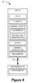
- FIG. 8illustrates a system in which disclosed embodiments of the disclosed techniques may be implemented, and illustrates an embodiment of the techniques in computer-readable media.
- a first methodcomprises determining a maximum voltage margin and a maximum timing margin of a received signal, and from these margins, determining an optimal sampling point, which includes a reference voltage level (Vref) and a relative sample phase.
- the location of the optimal sampling pointis based on the locations of the sampling point of the maximum voltage margin and the sampling point of the maximum timing margin.
- a second methodcomprises establishing an initial sampling point, and then successively refining each of the voltage and timing components of the sampling point until an optimal sampling point is reached.
- FIGS. 4A-4Dillustrate a first method for determining an optimal sampling point of a signal in accordance with one or more embodiments of the invention. Additionally, FIG. 4E illustrates a flow chart according to which an embodiment of the invention may be implemented. To simplify the FIGS. 4A-4D , the multiple samples as shown in FIG. 3 (e.g., 23 ) have been removed, and only the interior of the data eye 42 is illustrated.
- the interior of the data eye 42is “painted” in essentially the same manner as described in the background.
- the datais sampled over a certain number of cycles and the number of errors at each sampling point is computed.
- the sampled signal at each Vref/sample phase coordinateis compared to the current Vref at the point in time corresponding to the sample phase, and a determination is made as to whether an error has occurred.
- an optimal sampling pointis chosen to simultaneously optimize the voltage margin and the timing margin.
- the error-free Vref range (which is sometimes also referred to as a vertical opening) at each sample phase settingmay be calculated, for example, by sampling at incrementally increasing or decreasing Vref settings in each direction from the midpoint reference voltage 46 until an error or a certain number of errors is detected.
- the error-free Vref ranges at several sample phase settingsare represented by the vertical arrows 43 a - 43 c.
- a maximum voltage margin 43 cat one of the sample phase settings, is determined.
- the sample phase setting that results in the maximum error-free Vref rangeis identified as the setting of optimal phase.
- an associated optimal Vref settingis determined, and the coordinate of the optimal phase setting and the associated optimal Vref setting is stored.
- the coordinate comprising the sample phase and Vref level values, as shown in FIG. 4Amay be centered at the midpoint 48 of the maximum voltage margin 43 c.
- Vref level settingsA similar process is repeated for several Vref level settings. That is, the interior of the data eye 42 is sampled at multiple Vref levels to calculate the error-free sample phase range at each Vref level (i.e., the number of error-free phase settings). Each error-free sample phase range is represented by a horizontal arrow (e.g., 45 a - 45 c ) at each Vref setting.
- a maximum timing marginis determined and stored.
- the Vref level setting that results in the maximum error-free sample phase rangei.e., the largest timing margin, determined as having the most error-free phase settings
- an associated sample phase settingis determined, centered at the midpoint 50 of the maximum timing margin. This Vref/sample phase coordinate is also stored.
- an optimal sampling point 52may be determined.
- the optimal sampling point 52may be determined in a number of manners. For example, as shown in FIGS. 4C and 4D , the sampling points 48 and 50 may be averaged to determine an optimal sampling point. In other words, the voltage value of each sampling point 48 , 50 is averaged, and the sample phase value of each sample point 48 , 50 is also averaged. Such a method of averaging two coordinate points is well understood to one of ordinary skill in the art, and accordingly, is only briefly discussed here.
- the optimal sampling point 52is derived from an optimal sample phase value for sampling a signal (i.e., the best time in a given UI to sample the signal), as well as an optimal reference voltage level for determining the logic value of a signal.
- the optimal sampling point 52may then be used to sample future received signals in operations on the channel 14 . While this method shares a similar level of computational complexity with prior art methods, it leads to a sampling point that simultaneously maximizes the voltage margin and the timing margin of the system.
- FIGS. 5A-5Billustrate a second method for determining an optimal sampling point in accordance with one or more embodiments of the invention.
- FIG. 5Cillustrates a flow chart according to which an embodiment of the invention may be implemented.
- a data eye 42 of a received signal 15 bis shown in a window 40 .
- a midpoint sample phase 44 and a midpoint Vref level 46 of the data eye 42are also shown, each with a dashed line.
- this techniquecomprises establishing an initial sampling point 54 within the data eye 42 , and using measurements obtained at the sampling point 54 to adjust one or more components of the sampling point.
- the processbegins by sampling the data signal at a known Vref level and sample phase setting. Ideally, the initial setting combination will fall within the data eye. Whether this is true may be determined through sampling the signal over a certain number of cycles at the initial Vref/sample phase coordinate. If no errors (misinterpreted logic ‘1’ and logic ‘0’ values, etc.) are detected, the coordinate is assumed to fall within the data eye.
- the initial sampling point 54comprising a combined Vref level setting and a sample phase setting, may be chosen in a variety of ways. For example, an initial sampling point 54 may be randomly chosen and determined to fall within the eye based on the error calculation previously described. If errors occur, a new sampling point 54 could be chosen and the process repeated until a sampling point 54 is chosen which results in zero errors over a number of cycles. Regardless of the manner in which the initial sampling point 54 is derived, as long as the initial sampling point 54 is chosen such that it lies within the interior of the data eye 42 (error-free region), it is sufficient for the calculation of an optimal sampling point.
- Initializing the Vref/sample phase coordinate to a point within the eyemay be guaranteed through collaboration with the transmitter. Because clock-like signal patterns are known to result in zero ISI, if the transmitter begins the training sequence by transmitting a repeating ‘101010 . . . ’ pattern for a certain number of cycles, the clock and data edges may be aligned through phase detection circuitry. The initial Vref and sample phase setting may then be chosen by adding an amount of phase delay to the in-line clock timing and centering the Vref between the ideal signal swing levels (as specified in the system specification) to approach the center of the data eye. Once the initial Vref/sample phase coordinate has been established, the transmitter is free to transmit any arbitrary bit pattern.
- the horizontal distances 56 , 58are calculated from the current sample phase setting (i.e., the sample phase setting of the initial sampling point 54 ) to the first detected failure in each direction. This may be calculated in a number of manners. For example, if the incoming data is incrementally sampled at a number of sample phase intervals, the location of the first sample phase errors in each direction may be calculated by counting the number of incremental phase settings in each direction until the first detected failure is detected in a sample phase setting.
- Half of the difference between the horizontal distances 56 , 58which is represented by the arrow 59 , indicates a sample phase increment that may be added to the current sample phase setting of the initial sample point 54 .
- This corrected midpoint distance 59represents a preferred location of the sample phase for the received signal 15 b . Accordingly, this distance is added to the sample phase value of the initial sample point 54 to determine an updated sampling point 60 . It should be noted that at this time, only the sample phase of the sampling point, and not the Vref level, is updated.
- the vertical direction distances 62 , 64are calculated to determine a preferred Vref level setting for the sampling point 60 .
- the vertical distances 62 , 64may be calculated from the updated sampling point 60 to the first detected failure (i.e., at the interior of the data eye 42 ) in each direction.
- half of the difference between the vertical distances 62 , 64(which is quantified by the number of error-free Vref level settings), represented by the arrow 65 , indicates a Vref level increment that may be added to the current Vref level setting of the updated sampling point 60 to determine an updated sampling point 66 .
- the above processmay be repeated any number of times to adjust the optimal sampling point.
- a certain number of iterationsmay be employed.
- Experimental simulation analysisshows that two iterations (i.e., two corrections in each of the sample phase and Vref directions) may be sufficient to obtain an optimal sampling point 66 .
- a thresholdmay be set such that if an updated sampling point is within a certain number of Vref/sample phase settings from the current sampling point, then the process stops. In other words, if a difference between the current sampling point and the updated sampling point falls below a specified threshold, then the process stops.
- the above methodmay be modified in numerous manners. For example, although error-free sample phase ranges are determined before error-free Vref ranges to update the location of the sampling point, the error-free Vref ranges 62 , 64 may be determined before the error-free sample phase ranges 56 , 58 . Further, although the above processes describe comparing Vref and the sample phase to the sampled signal and determining whether an error is detected, any number of errors may be considered allowable when determining error-free Vref ranges or error-free sample phase ranges.
- FIG. 6is a block diagram of an exemplary processor system 70 within which a set of instructions, for causing the machine to perform any one or more of the techniques described herein, may be executed.
- the processor system 70may be present, for example, in the receiver 16 shown in FIG. 1 .
- the processor system 70operates as a standalone device or may be connected (e.g., networked) to other processor systems.
- the exemplary processor system 70includes a processor 72 (e.g., a central processing unit (CPU)) and a main memory 90 , which communicate with each other via one or more buses 94 .
- the CPU 72may further include an input/output (I/O) device 74 , a clock 76 , a control unit 78 , an arithmetic logic unit (ALU) 84 , registers 86 , and an instruction decoder 88 .
- I/Oinput/output
- ALUarithmetic logic unit
- the control unit 78includes a counter 80 and instruction registers 82 .
- the main memory 90includes a computer-readable medium 92 on which is stored one or more sets of instructions and/or data structures (e.g., software) embodying embodiments of the various techniques disclosed herein.
- the software 92may also reside, completely or at least partially, within the CPU 72 during execution thereof by the CPU 72 .
- a CPU 72 suitable for the execution of a computer programinclude, by way of example, both general and special purpose microprocessors, and any one or more processors of any kind of digital computer. Generally, a processor will receive instructions and data from a read-only memory or a random access memory or both. Further, one skilled in the art will appreciate that while the devices in FIG. 6 are shown having particular relationships (e.g., the main memory 90 is separate from the CPU 72 ), the various devices may be combined as shown or have other configurations.
- an input signal 101is received by a receiver circuit 102 , which compares the input signal 101 to Vref.
- the receiver circuitis controlled in part by a digital-to-analog converter (DAC) 106 and a Phase Interpolator (PI) 118 .
- the DAC 106controlled in turn by the control unit 104 , supplies a voltage (Vref) to the receiver circuit 102 for comparison to the input signal 101 .
- the PI 118controlled by the control unit 116 , supplies sample phase to the receiver circuit 102 to use when comparing Vref to the input signal 101 .
- the registers 108 , 114may be used to temporarily store Vref and sample phase settings in the DAC 106 and PI 118 , respectively.
- the receiver circuit 102may be a single-ended or differential receiver.
- the PI 118may include a number of elements, including, for example, a delay locked loop, to control the timing of the sample phase in the receiver circuit 102 .
- Embodiments according to the inventioninclude several advantages. For example, rather than repeating the error calculation at every testable Vref sample phase coordinate, the error may be calculated along specific coordinate axes, significantly reducing the number of training cycles that must be transmitted and the associated calibration time.
- the memory storage requirements of embodiments according to the inventionare also relaxed, as only a past updated sampling point coordinate and error counts along the current axis are stored from step to step through the process.
Landscapes
- Engineering & Computer Science (AREA)
- Computer Networks & Wireless Communication (AREA)
- Signal Processing (AREA)
- Power Engineering (AREA)
- Dc Digital Transmission (AREA)
Abstract
Description
- Embodiments of the invention relate to optimizing a sampling point of a received signal in an integrated circuit such as a Dynamic Random Access Memory (DRAM).
- Data transmission across high-speed chip-to-chip interconnects may take a number of forms. One example of a
data transmission system 10 between high-speed components within a single semiconductor device or between two devices on a printed circuit board is represented inFIG. 1 . InFIG. 1 , a transmitter12 (e.g., a microprocessor) sends data over one ormore transmission channels 14a-14c(e.g., copper traces “on-chip” in a semiconductor device or on a printed circuit board) to a receiver16 (e.g., another microprocessor or memory).Such transmission channels 14a-14care referred to, for example, as “data buses,” which allow one or more data signals to be transmitted from one device to another. Ideally, when a data signal is sent from atransmitter 12 to areceiver 16 across achannel 14, all of the energy in a transmitted pulse will be contained within a single time cell, which is often referred to as a unit interval (UI). - However, for a number of reasons, data signals are not received exactly as they were transmitted. While an ideal data signal may comprise a logic ‘1’ (“high”) value or a logic ‘0’ (“low”) value, a real data signal may become altered by the time it is detected at the
receiver 16. Often, this is a result of effects of the channel in which the data signals are sent. Thus, real transmitters and real transmission channels do not exhibit ideal characteristics, and the effects of transmission channels are becoming increasingly important in high-speed circuit design. Due to a number of factors, including, for example, the limited conductivity of copper traces, the dielectric medium of the printed circuit board (PCB), and the discontinuities introduced by vias, the initially well-defined digital pulse will tend to spread or disperse as it passes over the transmission path. - For example, the use of
multiple channels 14a-14cas shown inFIG. 1 may cause undesirable noise to be transferred from one data signal to another in thesystem 10 due to capacitive or inductive coupling between thechannels 14a-14c, in a phenomenon referred to as crosstalk. Even when only asingle channel 14 is present in asystem 10, a transmitted signal may be distorted due to capacitive or inductive effects. Inmulti-channel systems 10, crosstalk occurs when transitioning data induces either a voltage (inductive crosstalk) or a current (capacitive crosstalk) on a neighboring line. Crosstalk from neighboring channels may alter the amplitude and timing characteristics of a bit of interest on a given channel. Crosstalk is most often addressed with careful channel routing techniques, which may include the placement of additional traces between the channels to provide shielding and to reduce inter-channel coupling. - Another phenomenon leading to the distortion of data bits on a channel is dispersion, which results from non-uniform group delay or other bandwidth limitations on a
channel 14. This phenomenon results in the spreading of the energy of a pulse beyond the boundaries of the pulse UI, which results in energy from bits preceding or following a bit of interest in the bit sequence affecting the amplitude and/or timing of the bit of interest. This phenomenon is referred to as intersymbol interference (ISI) and is typically addressed through channel equalization. By either preceding or following the transmission channel with a frequency dependent circuit, whose transfer characteristics are the inverse of the channel characteristics, the original signal behavior may be restored. - Dispersion of a pulse is shown in
FIG. 2A , where a single pulse ofdata 15ais sent by thetransmitter 12 during a given UI (e.g., UI3). However, because of the effect of thechannel 14, this data pulse becomes spread15bover multiple UIs at thereceiver 16, i.e., some portion of the energy of the pulse is observed outside of the UI in which the pulse was sent (e.g., in UI2 and UI4). This residual energy outside of the UI of interest (ISI) may thus perturb a pulse otherwise occupying either of the neighboring UIs. - ISI is shown more succinctly in the simulation of
FIG. 2B , where two ideal pulses, π1and π2, each occupy their own adjacent unit intervals. The resulting dispersed pulses, P1and P2, represent simulated received versions of the ideal pulses after transmission at 10 Gb/s through a 6-inch copper trace in a standard printed circuit board material (FR4). The dispersion in each of these pulses overlaps the other pulse, as shown by the hatched portions in the drawings, which represent ISI. The larger pulse, P3, represents the waveform that results when P1and P2are sent across the same channel with no intermediate delay, which is a common occurrence in the standard non-return-to-zero (NRZ) signaling format. - From the perspective of the
receiver 16, one tool for quickly analyzing the effects of ISI and other noise on the signal is the eye diagram. An eye diagram is a plot that superimposes or overlays multiple data symbols from a data sequence. This provides a clear picture of how the data signal will change over time, and it also aids in determining the available margin for correct determination of the original digital state of each transmitted bit (i.e., that each transmitted bit is properly interpreted as a logic ‘1’ value or a logic ‘0’ value). When the eye closes, for example, due to reduced signal margins, the available data capture window shrinks and the probability of incorrectly interpreting the digital value of the received bit increases. - In high-speed systems, the ISI built up across the channel may be exacerbated or amplified in the receiver, if the receiver input buffer itself is bandwidth-limited or is intolerant to process variation. Thus, the technique of capturing the incoming data immediately as it enters the receiving chip, before it is passed through any circuitry, has been shown to provide the most margin for error in terms of the data capture mechanism, and as a result is becoming more commonplace in high performance systems.
- To capture the incoming data in this manner, a sense-amplifier is commonly used, which allows the data entering the receiving chip to be immediately compared with a reference voltage (Vref), at a point in time corresponding to a trigger from an associated clock edge (sample clock). Depending upon the receiver characteristics, this methodology can be extremely tolerant to amplitude noise- and timing jitter-induced data eye closure (i.e., the shrinkage of the data capture window). However, this method is sensitive to the relative position of Vref and the sample clock edge (phase relationship between clock and data transitions) with respect to the opening of the data eye.
- To reduce the probability of error, systems have begun to “train” Vref and the relative phase of the sampling clock edge in order to center the sample point (intersection of Vref and sample phase) within the capture window. Such training, which typically occurs during system startup, but may be repeated periodically throughout the operation of the system, may consist of interaction between the transmitter and receiver, or it may contained within the receiver, thus simplifying the interconnect. Such training may be carried out on a channel to channel basis (each receiver being trained independently), or the training may take place on a single channel with the resulting settings applied to several parallel receiver circuits to reduce area and power costs associated with instantiating several replicas of the training circuitry. In cases where only one channel is trained, and the resulting settings are applied to multiple channels, some additional receiver sensing margin is lost due to the channel-to-channel distinction inherent in real systems. In high speed systems, where the margins should be maximized, independent training of each channel is becoming more common. This can be done either by replicating the training circuitry at each receiver and performing the training of all channels simultaneously, or a single training circuit may be used, and time multiplexed between the various channels to train each channel, one at a time.
- Trainability of Vref implies that the magnitude of Vref is controllable. This typically requires Vref to be generated from a digital-to-analog converter (DAC), which can be set to output a specified voltage level on an analog signal based on a digital input. Similarly, trainability of the sample clock timing or sample phase relative to the data edge requires control over the clock propagation delay. This is typically accomplished through the employment of variable delay-lines (VDLs), which may or may not require the additional incorporation of a delay-locked loop (DLL) or a phase-locked loop (PLL). Further resolution in the sample phase setting is accomplished through phase interpolation circuits, which are also often controlled digitally.
- Thus, both Vref and the sample phase may be controlled digitally, and the range of each parameter may comprise several steps in voltage (Vref) or timing (sample phase), with the resolution of each step limited only by the level of complexity deemed appropriate for the system. The circuits required for these training operations, DACs, VDLs, DLLs, and PLLs, are well understood by one skilled in the art and are becoming more common in high performance systems. Thus, the circuitry itself is not considered a limiting factor when training Vref and the sample phase. Further, alternative methods for training, which may not require specific circuitry discussed here, are also possible.
- One method for training Vref and the sample phase to determine an optimal sampling point is discussed with reference to
FIG. 3A , which combines several cycles of data into an eye diagram, as discussed previously. It should be noted that the following descriptions are all discussed in terms of eye diagrams, which tend to imply that all of the information contained in the data eye is present at the outset of the training. On the contrary, the sampling of the data, as described throughout this specification, may be applied to real-time data and therefore information regarding the incoming signal is obtained gradually, and only by the end of the training sequence is all of the eye diagram information available. InFIG. 3A , anoptimal sample point 28 is determined by maximizing the voltage margin (represented by the arrows30) in theeye 22. This is done, in effect, by “painting” the eye, which comprises sampling the received signal as follows. - Essentially, at each available phase step, the error-free Vref range is determined by incrementing the Vref level, and at each incremented Vref level sampling the data for a certain number of cycles. The number of errors is computed for each Vref setting, at each phase step, and the error-free range is determined by counting the number of sequential Vref settings for which no errors were detected. The error-free range is then computed at each phase step, and from that data, the phase step which resulted in the largest error-free range is considered to provide the greatest voltage margin, (i.e., a distance from Vref to an error in the eye). As a result, the corresponding phase setting is adopted for real time operation and the Vref level is set to the midpoint of the corresponding error-free range (the setting for which an equal number of settings are above and below in the error-free range). At this point, the training is complete.
- One shortcoming with this approach is that determining the
optimal sampling point 28 by maximizing the voltage margin may result in offsetting the phase of thesampling point 28 from the optimal sampling phase, in this case themidpoint reference time 24. This is a common occurrence when maximizing the voltage margin, as the maximum voltage margin does not necessarily coincide with the maximum timing margin. Another shortcoming of this approach is the number of training cycles required by this method (i.e., the number of sampled cycles multiplied by the number of testable Vref/sample phase coordinates). In addition, the amount of data that must be stored throughout the training process can be problematic. At the very least, the process requires storing in memory the error-free range associated with each sample phase step. Further, in some implementations, this method may require storing the error count computed at each Vref/sample phase coordinate until the training is complete. - Another method used to determine an
optimal sampling point 34 is shown inFIG. 3B . InFIG. 3B , the concept of “painting” the eye is more clearly illustrated. The inside of theeye 22 is “painted” with several identically-sized squares, with each square corresponding to an independent Vref/sample phase setting combination, which is sometimes referred to herein as a coordinate. The inner opening of the data eye is determined in the manner just described, with regard toFIG. 3A , but in this case, theoptimal sampling point 34 is chosen to correspond to the most “central” coordinate (each being represented in the figure as a square). This is determined, for example, by locating a Vref/sample phase setting for which an equal number of error-free voltage settings are above and below, and for which an equal number of error-free phase settings are before and after in time (i.e., for each sample phase setting). Such a Vref/sample phase setting constitutes the optimal sampling point. After this point is determined, the training is complete. - Although determination of the
optimal sampling point 34 according toFIG. 3B provides a more accurate sampling point than simply taking the widest voltage margin, as it also gives consideration to the timing margin, this method is computationally expensive, requiring numerous calculations to paint theeye 22 and determine thecentral sampling point 34, and further requires storing the error count at each testable Vref/sample phase coordinate, or at least storing the Vref and sample phase settings associated with each coordinate along the inner eye boundary, until the training is completed. - As was noted previously, the implementation of the above training algorithms takes place in the presence of real time data. In other words, data transitions are not guaranteed and the state of the data is not known in advance, though a replica of the training pattern may be stored in the receiving circuitry to simplify the process. It should also be pointed out that the term “optimal” is subjective. No method identifies a single “optimal” sampling point (i.e., a combined Vref and sample phase coordinate) in terms of providing for the lowest probability of error for all instances of a received signal. Rather, each method determines the best sampling point for a given amount of information obtainable by the receiver system.
- Clearly, circuit designers of multi-Gigabit systems face a number of challenges as advances in technology mandate increased performance in high-speed systems. Correct detection of such high-speed signals becomes difficult as data rates and physical constraints on transmission circuits increase. Accordingly, an improved technique for determining an optimal sampling point for the data capture process would do so in a computationally efficient manner. The disclosed techniques achieve such results in a manner implemented in a typical computerized system or other circuit package.
FIG. 1 illustrates a block diagram of a transmission system on a printed circuit board.FIGS. 2A and 2B illustrate the effect of a transmission channel on pulses sent across the channel, and in particular show intersymbol interference (ISI).FIGS. 3A and 3B illustrate methods for calculating the location of a sampling point.FIGS. 4A-4D illustrate a method for calculating the location of a sampling point in accordance with an embodiment of the invention.FIG. 4E illustrates a computer-implementable flow chart illustrating an embodiment of the invention.FIGS. 5A-5B illustrate a method for calculating the location of a sampling point in accordance with an embodiment of the invention.FIG. 5C illustrates a computer-implementable flow chart illustrating an embodiment of the invention.FIG. 6 illustrates a processor in which disclosed embodiments of the disclosed techniques may be implemented, and illustrates an embodiment of the techniques in computer-readable media.FIG. 7 illustrates a system in which disclosed embodiments of the disclosed techniques may be implemented, and illustrates an embodiment of the techniques in computer-readable media.FIG. 8 illustrates a system in which disclosed embodiments of the disclosed techniques may be implemented, and illustrates an embodiment of the techniques in computer-readable media.- Methods and apparatuses for calculating the location of an optimal sampling point for a receiver system are disclosed. In brief, in one or more embodiments according to the invention, a first method comprises determining a maximum voltage margin and a maximum timing margin of a received signal, and from these margins, determining an optimal sampling point, which includes a reference voltage level (Vref) and a relative sample phase. The location of the optimal sampling point is based on the locations of the sampling point of the maximum voltage margin and the sampling point of the maximum timing margin. A second method comprises establishing an initial sampling point, and then successively refining each of the voltage and timing components of the sampling point until an optimal sampling point is reached.
FIGS. 4A-4D illustrate a first method for determining an optimal sampling point of a signal in accordance with one or more embodiments of the invention. Additionally,FIG. 4E illustrates a flow chart according to which an embodiment of the invention may be implemented. To simplify theFIGS. 4A-4D , the multiple samples as shown inFIG. 3 (e.g.,23) have been removed, and only the interior of thedata eye 42 is illustrated.- According to the embodiment shown in
FIGS. 4A-4D , initially, the interior of thedata eye 42 is “painted” in essentially the same manner as described in the background. At each combined Vref/sample phase coordinate, the data is sampled over a certain number of cycles and the number of errors at each sampling point is computed. In other words, the sampled signal at each Vref/sample phase coordinate is compared to the current Vref at the point in time corresponding to the sample phase, and a determination is made as to whether an error has occurred. Based on the error-free region within the data eye opening, an optimal sampling point is chosen to simultaneously optimize the voltage margin and the timing margin. To reduce the number of required samples, the error-free Vref range (which is sometimes also referred to as a vertical opening) at each sample phase setting may be calculated, for example, by sampling at incrementally increasing or decreasing Vref settings in each direction from themidpoint reference voltage 46 until an error or a certain number of errors is detected. The error-free Vref ranges at several sample phase settings are represented by the vertical arrows43a-43c. - After all of the phases have been sampled, a
maximum voltage margin 43c, at one of the sample phase settings, is determined. In other words, the sample phase setting that results in the maximum error-free Vref range is identified as the setting of optimal phase. At this optimal phase, an associated optimal Vref setting is determined, and the coordinate of the optimal phase setting and the associated optimal Vref setting is stored. The coordinate comprising the sample phase and Vref level values, as shown inFIG. 4A , may be centered at themidpoint 48 of themaximum voltage margin 43c. - A similar process is repeated for several Vref level settings. That is, the interior of the
data eye 42 is sampled at multiple Vref levels to calculate the error-free sample phase range at each Vref level (i.e., the number of error-free phase settings). Each error-free sample phase range is represented by a horizontal arrow (e.g.,45a-45c) at each Vref setting. After all Vref levels have been sampled and the corresponding error-free sample phase ranges have been obtained, a maximum timing margin is determined and stored. In other words, the Vref level setting that results in the maximum error-free sample phase range (i.e., the largest timing margin, determined as having the most error-free phase settings) is identified as the optimal Vref level for the signal. At this optimal Vref level, an associated sample phase setting is determined, centered at themidpoint 50 of the maximum timing margin. This Vref/sample phase coordinate is also stored. - Based on the
sampling point 48 of the maximum voltage margin and thesampling point 50 of the maximum timing margin, anoptimal sampling point 52 may be determined. Theoptimal sampling point 52 may be determined in a number of manners. For example, as shown inFIGS. 4C and 4D , the sampling points48 and50 may be averaged to determine an optimal sampling point. In other words, the voltage value of eachsampling point sample point optimal sampling point 52 is derived from an optimal sample phase value for sampling a signal (i.e., the best time in a given UI to sample the signal), as well as an optimal reference voltage level for determining the logic value of a signal. Theoptimal sampling point 52 may then be used to sample future received signals in operations on thechannel 14. While this method shares a similar level of computational complexity with prior art methods, it leads to a sampling point that simultaneously maximizes the voltage margin and the timing margin of the system. FIGS. 5A-5B illustrate a second method for determining an optimal sampling point in accordance with one or more embodiments of the invention. In addition,FIG. 5C illustrates a flow chart according to which an embodiment of the invention may be implemented. InFIG. 5A , adata eye 42 of a receivedsignal 15bis shown in awindow 40. For reference, amidpoint sample phase 44 and amidpoint Vref level 46 of thedata eye 42 are also shown, each with a dashed line. In brief, this technique comprises establishing aninitial sampling point 54 within thedata eye 42, and using measurements obtained at thesampling point 54 to adjust one or more components of the sampling point.- The process begins by sampling the data signal at a known Vref level and sample phase setting. Ideally, the initial setting combination will fall within the data eye. Whether this is true may be determined through sampling the signal over a certain number of cycles at the initial Vref/sample phase coordinate. If no errors (misinterpreted logic ‘1’ and logic ‘0’ values, etc.) are detected, the coordinate is assumed to fall within the data eye.
- The
initial sampling point 54, comprising a combined Vref level setting and a sample phase setting, may be chosen in a variety of ways. For example, aninitial sampling point 54 may be randomly chosen and determined to fall within the eye based on the error calculation previously described. If errors occur, anew sampling point 54 could be chosen and the process repeated until asampling point 54 is chosen which results in zero errors over a number of cycles. Regardless of the manner in which theinitial sampling point 54 is derived, as long as theinitial sampling point 54 is chosen such that it lies within the interior of the data eye42 (error-free region), it is sufficient for the calculation of an optimal sampling point. - Initializing the Vref/sample phase coordinate to a point within the eye may be guaranteed through collaboration with the transmitter. Because clock-like signal patterns are known to result in zero ISI, if the transmitter begins the training sequence by transmitting a repeating ‘101010 . . . ’ pattern for a certain number of cycles, the clock and data edges may be aligned through phase detection circuitry. The initial Vref and sample phase setting may then be chosen by adding an amount of phase delay to the in-line clock timing and centering the Vref between the ideal signal swing levels (as specified in the system specification) to approach the center of the data eye. Once the initial Vref/sample phase coordinate has been established, the transmitter is free to transmit any arbitrary bit pattern.
- From the
initial sampling point 54, thehorizontal distances horizontal distances arrow 59, indicates a sample phase increment that may be added to the current sample phase setting of theinitial sample point 54. This correctedmidpoint distance 59 represents a preferred location of the sample phase for the receivedsignal 15b. Accordingly, this distance is added to the sample phase value of theinitial sample point 54 to determine an updatedsampling point 60. It should be noted that at this time, only the sample phase of the sampling point, and not the Vref level, is updated. - From the updated
sampling point 60, a process similar to the above-described process is performed to update the Vref level of the updatedsampling point 60. In other words, the vertical direction distances62,64, are calculated to determine a preferred Vref level setting for thesampling point 60. The vertical distances62,64 may be calculated from the updatedsampling point 60 to the first detected failure (i.e., at the interior of the data eye42) in each direction. As in the case with the updated sample phase value, half of the difference between thevertical distances 62,64 (which is quantified by the number of error-free Vref level settings), represented by thearrow 65, indicates a Vref level increment that may be added to the current Vref level setting of the updatedsampling point 60 to determine an updatedsampling point 66. - The above process may be repeated any number of times to adjust the optimal sampling point. In one or more embodiments according to the invention, a certain number of iterations may be employed. Experimental simulation analysis shows that two iterations (i.e., two corrections in each of the sample phase and Vref directions) may be sufficient to obtain an
optimal sampling point 66. In one or more alternative embodiments, a threshold may be set such that if an updated sampling point is within a certain number of Vref/sample phase settings from the current sampling point, then the process stops. In other words, if a difference between the current sampling point and the updated sampling point falls below a specified threshold, then the process stops. - Further, the above method may be modified in numerous manners. For example, although error-free sample phase ranges are determined before error-free Vref ranges to update the location of the sampling point, the error-free Vref ranges62,64 may be determined before the error-free sample phase ranges56,58. Further, although the above processes describe comparing Vref and the sample phase to the sampled signal and determining whether an error is detected, any number of errors may be considered allowable when determining error-free Vref ranges or error-free sample phase ranges.
FIG. 6 is a block diagram of anexemplary processor system 70 within which a set of instructions, for causing the machine to perform any one or more of the techniques described herein, may be executed. Theprocessor system 70 may be present, for example, in thereceiver 16 shown inFIG. 1 . In alternative embodiments, theprocessor system 70 operates as a standalone device or may be connected (e.g., networked) to other processor systems.- The
exemplary processor system 70 includes a processor72 (e.g., a central processing unit (CPU)) and amain memory 90, which communicate with each other via one ormore buses 94. TheCPU 72 may further include an input/output (I/O)device 74, aclock 76, acontrol unit 78, an arithmetic logic unit (ALU)84, registers86, and aninstruction decoder 88. - The
control unit 78 includes acounter 80 and instruction registers82. Themain memory 90 includes a computer-readable medium 92 on which is stored one or more sets of instructions and/or data structures (e.g., software) embodying embodiments of the various techniques disclosed herein. Thesoftware 92 may also reside, completely or at least partially, within theCPU 72 during execution thereof by theCPU 72. - A
CPU 72 suitable for the execution of a computer program include, by way of example, both general and special purpose microprocessors, and any one or more processors of any kind of digital computer. Generally, a processor will receive instructions and data from a read-only memory or a random access memory or both. Further, one skilled in the art will appreciate that while the devices inFIG. 6 are shown having particular relationships (e.g., themain memory 90 is separate from the CPU72), the various devices may be combined as shown or have other configurations. - While the
software 92 is shown in the exemplary embodiment ofFIG. 6 to be a single medium, the term “computer-readable medium” should be taken to include a single medium or multiple media that store the one or more sets of instructions. The term “computer-readable medium” shall also be taken to include any medium that is capable of storing, encoding or carrying a set of instructions for execution by the machine and that cause the machine to perform any one or more of the methodologies of the disclosed techniques, or that is capable of storing, encoding or carrying data structures utilized by or associated with such a set of instructions. The term “computer-readable medium” shall accordingly be taken to include, but not be limited to, solid-state memories, optical and magnetic media such as discs, and carrier wave signals. - Embodiments of the disclosed techniques can also be implemented in digital electronic circuitry, in computer hardware, in firmware, in special purpose logic circuitry such as an FPGA (field programmable gate array) or an ASIC (application-specific integrated circuit), in software, or in combinations of the above, which again all comprise examples of “computer-readable media.” One
such system 100 is shown inFIG. 7 . - In brief, the
system 100 may be used to train thereceiver circuit 102 to determine the most accurate location of a sample point for theinput signal 101 that it receives. This may be accomplished, for example, by transmitting on the input signal101 a known data sequence to thesystem 100. If thesystem 100 also knows the data sequence, thesystem 100 can make determinations as to when theinput signal 101 is correctly or incorrectly interpreted. Incorrect interpretations lead to adjustment of the sample point. Such asystem 100 may further be used in conjunction with the methods discussed above. - In
FIG. 7 , aninput signal 101 is received by areceiver circuit 102, which compares theinput signal 101 to Vref. The receiver circuit is controlled in part by a digital-to-analog converter (DAC)106 and a Phase Interpolator (PI)118. TheDAC 106, controlled in turn by thecontrol unit 104, supplies a voltage (Vref) to thereceiver circuit 102 for comparison to theinput signal 101. ThePI 118, controlled by thecontrol unit 116, supplies sample phase to thereceiver circuit 102 to use when comparing Vref to theinput signal 101. Theregisters DAC 106 andPI 118, respectively. - It should be noted that the
DAC 106 is not required to output a voltage for comparison with the data at thereceiver circuit 102. For example, when thereceiver circuit 102 is implemented as a differential sense-amplifier, a fixed Vref level may be applied to the comparison input, and the current through the differential legs of the sense-amplifier may be incrementally skewed by theDAC 106 in a way equivalent to incrementing the comparison voltage. Such an implementation may be used, for example, in a fully-differential (versus a single-ended) system. - After a comparison between the
input signal 101 and Vref is made in thereceiver circuit 102, the results are output and also sent to anerror calculator 110. Theerror calculator 110 is provided with the known training sequence, and thus is capable of providing feedback to thestate machine 112 regarding the sampled value of theinput signal 101 determined by thereceiver circuit 102. In combination with error signals sent from theerror calculator 110 to thestate machine 112, the state machine determines which Vref and sample phase settings used by theDAC 106 and PI118 (in theregisters 108,114) result in correct and incorrect samples of theinput signal 101. Accordingly, the state machine is then capable of adjusting Vref and the sample phase settings used in thereceiver circuit 102, via thecontrol units DAC 106 andPI 118. - While the components of the
system 100 are shown as functional units, one skilled in the art will appreciate that several components are available that may be used in thesystem 100. For example, thereceiver circuit 102 may be a single-ended or differential receiver. Similarly, thePI 118 may include a number of elements, including, for example, a delay locked loop, to control the timing of the sample phase in thereceiver circuit 102. - As described previously, the training circuit may be shared by each channel on the bus or replicas of certain components of the training system may be instantiated locally at each receiver. Such a case is illustrated in
FIG. 8 . To provide simultaneous and independent tuning of each channel on the bus, theDAC 106,PI 118,control units FIG. 7 become DAC<0:N>126, PI<0:N>138, control units<0:N>124,136, and registers128,134, as shown inFIG. 8 , where N equals the number of channels on thebus 140. Control of these components insystem 120 may be accomplished simultaneously from asingle state machine 132. Other devices, such as the receiver circuit<0:N>122 and error calculator<0:N>130, function as described above, with the additional functionality of being capable of handling multiple input signals121 andinput clocks 137, from thechannels 14, on thebus 140. - When implemented as software, such software can be written in any form of programming language, including compiled or interpreted languages, and it can be deployed in any form, including as a stand-alone program or as a module, component, subroutine, or other unit suitable for use in a computing environment. A computer program can be deployed to be executed on one computer or on multiple computers at one site or distributed across multiple sites and interconnected by a communication network.
- Embodiments according to the invention include several advantages. For example, rather than repeating the error calculation at every testable Vref sample phase coordinate, the error may be calculated along specific coordinate axes, significantly reducing the number of training cycles that must be transmitted and the associated calibration time. The memory storage requirements of embodiments according to the invention are also relaxed, as only a past updated sampling point coordinate and error counts along the current axis are stored from step to step through the process.
- As an advantage of the various disclosed techniques, a balance may be found between maximizing a voltage margin and a timing margin of a received signal. Further, the amount of processing and memory necessary to determine a voltage or timing margin may be reduced. Further, a number of calibration steps (i.e., iterations to an optimal value) may be reduced. In other words, an optimal sampling point may be determined from less data and with less computational complexity than with other methods.
- While preferred embodiments of the invention have been disclosed, it should be understood that the disclosed circuitry can be achieved in many different ways to the same useful ends as described herein. In short, it should be understood that the inventive concepts disclosed herein are capable of many modifications. To the extent such modifications fall within the scope of the appended claims and their equivalents, they are intended to be covered by this patent.
Claims (25)
Priority Applications (6)
| Application Number | Priority Date | Filing Date | Title |
|---|---|---|---|
| US11/930,524US7991098B2 (en) | 2007-10-31 | 2007-10-31 | Method and apparatus for training the reference voltage level and data sample timing in a receiver |
| CN200880113749XACN101842776B (en) | 2007-10-31 | 2008-10-08 | Method and apparatus for training reference voltage level and data sample timing in a receiver |
| KR1020107009495AKR101114117B1 (en) | 2007-10-31 | 2008-10-08 | Method and apparatus for training the reference voltage level and data sample timing in a receiver |
| PCT/US2008/079165WO2009058529A1 (en) | 2007-10-31 | 2008-10-08 | Method and apparatus for training reference voltage level and data sample timing in a receiver |
| TW097140697ATWI355586B (en) | 2007-10-31 | 2008-10-23 | Method and apparatus for training the reference vo |
| US13/187,053US8599967B2 (en) | 2007-10-31 | 2011-07-20 | Method and apparatus for training the reference voltage level and data sample timing in a receiver |
Applications Claiming Priority (1)
| Application Number | Priority Date | Filing Date | Title |
|---|---|---|---|
| US11/930,524US7991098B2 (en) | 2007-10-31 | 2007-10-31 | Method and apparatus for training the reference voltage level and data sample timing in a receiver |
Related Child Applications (1)
| Application Number | Title | Priority Date | Filing Date |
|---|---|---|---|
| US13/187,053ContinuationUS8599967B2 (en) | 2007-10-31 | 2011-07-20 | Method and apparatus for training the reference voltage level and data sample timing in a receiver |
Publications (2)
| Publication Number | Publication Date |
|---|---|
| US20090110116A1true US20090110116A1 (en) | 2009-04-30 |
| US7991098B2 US7991098B2 (en) | 2011-08-02 |
Family
ID=40582826
Family Applications (2)
| Application Number | Title | Priority Date | Filing Date |
|---|---|---|---|
| US11/930,524Active2030-06-01US7991098B2 (en) | 2007-10-31 | 2007-10-31 | Method and apparatus for training the reference voltage level and data sample timing in a receiver |
| US13/187,053Active2028-01-28US8599967B2 (en) | 2007-10-31 | 2011-07-20 | Method and apparatus for training the reference voltage level and data sample timing in a receiver |
Family Applications After (1)
| Application Number | Title | Priority Date | Filing Date |
|---|---|---|---|
| US13/187,053Active2028-01-28US8599967B2 (en) | 2007-10-31 | 2011-07-20 | Method and apparatus for training the reference voltage level and data sample timing in a receiver |
Country Status (5)
| Country | Link |
|---|---|
| US (2) | US7991098B2 (en) |
| KR (1) | KR101114117B1 (en) |
| CN (1) | CN101842776B (en) |
| TW (1) | TWI355586B (en) |
| WO (1) | WO2009058529A1 (en) |
Cited By (16)
| Publication number | Priority date | Publication date | Assignee | Title |
|---|---|---|---|---|
| US20100283503A1 (en)* | 2009-05-06 | 2010-11-11 | Micron Technology, Inc. | Reference voltage circuits and on-die termination circuits, methods for updating the same, and methods for tracking supply, temperature, and/or process variation |
| US8504334B2 (en) | 2010-07-16 | 2013-08-06 | Micron Technology, Inc. | Simulating the transmission and simultaneous switching output noise of signals in a computer system |
| US8510092B2 (en) | 2011-01-07 | 2013-08-13 | Micron Technology, Inc. | Recursive summation algorithms useful for statistical signal analysis of transmission of signals in a computer system |
| US20130307607A1 (en)* | 2012-04-27 | 2013-11-21 | Rambus Inc. | Simultaneous switching noise cancellation by adjusting reference voltage and sampling clock phase |
| US8682621B2 (en) | 2010-07-16 | 2014-03-25 | Micron Technology, Inc. | Simulating the transmission of asymmetric signals in a computer system |
| US20140181429A1 (en)* | 2012-12-26 | 2014-06-26 | Nvidia Corporation | Multi-dimensional hardware data training between memory controller and memory |
| US20160232962A1 (en)* | 2009-12-15 | 2016-08-11 | Intel Corporation | Method and apparatus for dynamically adjusting voltage reference to optimize an i/o system |
| US9824772B2 (en) | 2012-12-26 | 2017-11-21 | Nvidia Corporation | Hardware chip select training for memory using read commands |
| US9891853B1 (en)* | 2016-01-19 | 2018-02-13 | Apple Inc. | Memory calibration abort |
| US9971975B2 (en)* | 2016-05-09 | 2018-05-15 | Invecas, Inc. | Optimal data eye for improved Vref margin |
| US20200118137A1 (en)* | 2018-10-15 | 2020-04-16 | Priv8Pay, Inc. | Transaction management system |
| KR20200048607A (en)* | 2018-10-30 | 2020-05-08 | 삼성전자주식회사 | System on chip performing training of duty cycle of write clock using mode register write command, operating method of system on chip, electronic device including system on chip |
| KR20200049985A (en)* | 2018-10-30 | 2020-05-11 | 삼성전자주식회사 | System on chip performining a plurality of trainings at the same time, operating method of system on chip, electronic device including system on chip |
| CN112231255A (en)* | 2015-03-26 | 2021-01-15 | 英特尔公司 | Multichip Package Link |
| KR20210099662A (en)* | 2017-03-21 | 2021-08-12 | 마이크론 테크놀로지, 인크. | Timing control for input receiver |
| JP2022534651A (en)* | 2019-05-24 | 2022-08-03 | インテル・コーポレーション | Training for chip select signal read operation by memory device |
Families Citing this family (30)
| Publication number | Priority date | Publication date | Assignee | Title |
|---|---|---|---|---|
| US7991098B2 (en)* | 2007-10-31 | 2011-08-02 | Micron Technology, Inc. | Method and apparatus for training the reference voltage level and data sample timing in a receiver |
| JP5211122B2 (en)* | 2010-08-31 | 2013-06-12 | 株式会社アドバンテスト | Sampling device and test device |
| US8451969B2 (en)* | 2011-03-15 | 2013-05-28 | Intel Corporation | Apparatus, system, and method for timing recovery |
| US8850155B2 (en) | 2011-12-19 | 2014-09-30 | Advanced Micro Devices, Inc. | DDR 2D Vref training |
| WO2013119209A1 (en) | 2012-02-07 | 2013-08-15 | Intel Corporation | Gated ring oscillator-based digital eye width monitor for high-speed i/o eye width measurement |
| US8923442B2 (en) | 2012-02-08 | 2014-12-30 | Rambus Inc. | Reference voltage generation in a single-ended receiver |
| US8837653B2 (en)* | 2012-06-08 | 2014-09-16 | Deere & Company | High frequency signal receiver with self-calibrated group delay compensation |
| US8837654B2 (en)* | 2012-06-08 | 2014-09-16 | Deere & Company | Signal receiver with group delay and amplitude distortion compensation |
| US8929499B2 (en)* | 2012-09-29 | 2015-01-06 | Intel Corporation | System timing margin improvement of high speed I/O interconnect links by using fine training of phase interpolator |
| US9525571B2 (en) | 2013-03-05 | 2016-12-20 | Lattice Semiconductor Corporation | Calibration of single-ended high-speed interfaces |
| TWI561006B (en)* | 2013-05-24 | 2016-12-01 | Marvell Israel Misl Ltd | Systems and methods for data receipt from devices of disparate types |
| CN104391464B (en)* | 2014-11-06 | 2017-04-05 | 电子科技大学 | A kind of hardware equivalent synchronized sampling unit based on FPGA |
| KR102282401B1 (en) | 2015-01-02 | 2021-07-26 | 삼성전자주식회사 | Device and Method for training reference voltage |
| JP6387883B2 (en) | 2015-04-02 | 2018-09-12 | 富士通株式会社 | Information processing apparatus, information processing system, information processing apparatus control program, and information processing apparatus control method |
| US9401721B1 (en) | 2015-06-16 | 2016-07-26 | Advanced Micro Devices, Inc. | Reference voltage generation and tuning |
| KR102447493B1 (en) | 2017-12-04 | 2022-09-26 | 삼성전자주식회사 | Electronic device for training memory device in rank units and memory training method thereof |
| JP6672376B2 (en)* | 2018-05-16 | 2020-03-25 | アンリツ株式会社 | Error rate measuring device and parameter searching method of the device |
| US10997095B2 (en)* | 2018-08-21 | 2021-05-04 | Micron Technology, Inc. | Training procedure for receivers associated with a memory device |
| WO2020256165A1 (en)* | 2019-06-18 | 2020-12-24 | 엘지전자 주식회사 | Signal receiving method, and signal receiving multimedia device |
| FR3101218B1 (en) | 2019-09-23 | 2022-07-01 | Macom Tech Solutions Holdings Inc | EQUALIZER ADAPTATION BASED ON EYE MONITORING DEVICE MEASUREMENTS |
| WO2021076800A1 (en)* | 2019-10-15 | 2021-04-22 | Macom Technology Solutions Holdings, Inc. | Finding the eye center with a low-power eye monitor using a 3-dimensional algorithm |
| WO2021142216A1 (en) | 2020-01-10 | 2021-07-15 | Macom Technology Solutions Holdings, Inc. | Optimal equalization partitioning |
| US11575437B2 (en) | 2020-01-10 | 2023-02-07 | Macom Technology Solutions Holdings, Inc. | Optimal equalization partitioning |
| US11323296B1 (en)* | 2020-07-30 | 2022-05-03 | Cadence Design Systems, Inc. | Decision feedback equalization training scheme for GDDR applications |
| US11616529B2 (en) | 2021-02-12 | 2023-03-28 | Macom Technology Solutions Holdings, Inc. | Adaptive cable equalizer |
| KR20220144091A (en) | 2021-04-19 | 2022-10-26 | 삼성전자주식회사 | Method for operating host device and memory device and vehicle comprising the host device and memory device |
| US12367943B2 (en)* | 2021-06-25 | 2025-07-22 | Intel Corporation | Reference voltage adjustment per path for high speed memory signaling |
| US12204751B2 (en) | 2021-06-25 | 2025-01-21 | Intel Corporation | Reference voltage training per path for high speed memory signaling |
| US11947382B2 (en)* | 2022-07-29 | 2024-04-02 | Micron Technology, Inc. | Measuring a timing margin of a memory device using an internal oscilloscope |
| KR102821901B1 (en)* | 2023-12-28 | 2025-06-18 | 인하대학교 산학협력단 | Dual Self-Training Calibration Method and System for VREF Generator for Memory Interface |
Citations (6)
| Publication number | Priority date | Publication date | Assignee | Title |
|---|---|---|---|---|
| US6519302B1 (en)* | 1999-11-24 | 2003-02-11 | Nortel Networks Limited | Method and apparatus for regenerating data |
| US6760676B2 (en)* | 2002-07-31 | 2004-07-06 | Agilent Technologies, Inc. | On-screen tools for eye diagram measurements |
| US6914947B2 (en)* | 2001-02-28 | 2005-07-05 | Telefonaktiebolaget L M Ericsson (Publ) | Method and apparatus for handling time-drift |
| US20050259774A1 (en)* | 2004-05-18 | 2005-11-24 | Garlepp Bruno W | Statistical margin test methods and circuits |
| US7036053B2 (en)* | 2002-12-19 | 2006-04-25 | Intel Corporation | Two dimensional data eye centering for source synchronous data transfers |
| US7039328B2 (en)* | 2001-04-26 | 2006-05-02 | Sumitomo Electric Industries, Ltd. | Data regenerator and optical receiver |
Family Cites Families (2)
| Publication number | Priority date | Publication date | Assignee | Title |
|---|---|---|---|---|
| US7729465B2 (en) | 2006-03-06 | 2010-06-01 | Globalfoundries Inc. | Asymmetric control of high-speed bidirectional signaling |
| US7991098B2 (en)* | 2007-10-31 | 2011-08-02 | Micron Technology, Inc. | Method and apparatus for training the reference voltage level and data sample timing in a receiver |
- 2007
- 2007-10-31USUS11/930,524patent/US7991098B2/enactiveActive
- 2008
- 2008-10-08KRKR1020107009495Apatent/KR101114117B1/enactiveActive
- 2008-10-08CNCN200880113749XApatent/CN101842776B/enactiveActive
- 2008-10-08WOPCT/US2008/079165patent/WO2009058529A1/enactiveApplication Filing
- 2008-10-23TWTW097140697Apatent/TWI355586B/enactive
- 2011
- 2011-07-20USUS13/187,053patent/US8599967B2/enactiveActive
Patent Citations (6)
| Publication number | Priority date | Publication date | Assignee | Title |
|---|---|---|---|---|
| US6519302B1 (en)* | 1999-11-24 | 2003-02-11 | Nortel Networks Limited | Method and apparatus for regenerating data |
| US6914947B2 (en)* | 2001-02-28 | 2005-07-05 | Telefonaktiebolaget L M Ericsson (Publ) | Method and apparatus for handling time-drift |
| US7039328B2 (en)* | 2001-04-26 | 2006-05-02 | Sumitomo Electric Industries, Ltd. | Data regenerator and optical receiver |
| US6760676B2 (en)* | 2002-07-31 | 2004-07-06 | Agilent Technologies, Inc. | On-screen tools for eye diagram measurements |
| US7036053B2 (en)* | 2002-12-19 | 2006-04-25 | Intel Corporation | Two dimensional data eye centering for source synchronous data transfers |
| US20050259774A1 (en)* | 2004-05-18 | 2005-11-24 | Garlepp Bruno W | Statistical margin test methods and circuits |
Cited By (26)
| Publication number | Priority date | Publication date | Assignee | Title |
|---|---|---|---|---|
| US9608630B2 (en) | 2009-05-06 | 2017-03-28 | Micron Technology, Inc. | Reference voltage circuits and on-die termination circuits, methods for updating the same, and methods for tracking supply, temperature, and/or process variation |
| US20100283503A1 (en)* | 2009-05-06 | 2010-11-11 | Micron Technology, Inc. | Reference voltage circuits and on-die termination circuits, methods for updating the same, and methods for tracking supply, temperature, and/or process variation |
| US10347319B2 (en)* | 2009-12-15 | 2019-07-09 | Intel Corporation | Method and apparatus for dynamically adjusting voltage reference to optimize an I/O system |
| US20160232962A1 (en)* | 2009-12-15 | 2016-08-11 | Intel Corporation | Method and apparatus for dynamically adjusting voltage reference to optimize an i/o system |
| US8504334B2 (en) | 2010-07-16 | 2013-08-06 | Micron Technology, Inc. | Simulating the transmission and simultaneous switching output noise of signals in a computer system |
| US8682621B2 (en) | 2010-07-16 | 2014-03-25 | Micron Technology, Inc. | Simulating the transmission of asymmetric signals in a computer system |
| US8938376B2 (en) | 2010-07-16 | 2015-01-20 | Micron Technology, Inc. | Simulating the transmission and simultaneous switching output noise of signals in a computer system |
| US8510092B2 (en) | 2011-01-07 | 2013-08-13 | Micron Technology, Inc. | Recursive summation algorithms useful for statistical signal analysis of transmission of signals in a computer system |
| US20130307607A1 (en)* | 2012-04-27 | 2013-11-21 | Rambus Inc. | Simultaneous switching noise cancellation by adjusting reference voltage and sampling clock phase |
| US8878592B2 (en)* | 2012-04-27 | 2014-11-04 | Rambus Inc. | Simultaneous switching noise cancellation by adjusting reference voltage and sampling clock phase |
| US20140181429A1 (en)* | 2012-12-26 | 2014-06-26 | Nvidia Corporation | Multi-dimensional hardware data training between memory controller and memory |
| US9824772B2 (en) | 2012-12-26 | 2017-11-21 | Nvidia Corporation | Hardware chip select training for memory using read commands |
| EP3796181A1 (en)* | 2015-03-26 | 2021-03-24 | INTEL Corporation | Multichip package link |
| CN112231255A (en)* | 2015-03-26 | 2021-01-15 | 英特尔公司 | Multichip Package Link |
| US9891853B1 (en)* | 2016-01-19 | 2018-02-13 | Apple Inc. | Memory calibration abort |
| US9971975B2 (en)* | 2016-05-09 | 2018-05-15 | Invecas, Inc. | Optimal data eye for improved Vref margin |
| KR20210099662A (en)* | 2017-03-21 | 2021-08-12 | 마이크론 테크놀로지, 인크. | Timing control for input receiver |
| KR102401875B1 (en)* | 2017-03-21 | 2022-05-25 | 마이크론 테크놀로지, 인크. | Timing control for input receiver |
| US20200118137A1 (en)* | 2018-10-15 | 2020-04-16 | Priv8Pay, Inc. | Transaction management system |
| KR20200049985A (en)* | 2018-10-30 | 2020-05-11 | 삼성전자주식회사 | System on chip performining a plurality of trainings at the same time, operating method of system on chip, electronic device including system on chip |
| KR20200048607A (en)* | 2018-10-30 | 2020-05-08 | 삼성전자주식회사 | System on chip performing training of duty cycle of write clock using mode register write command, operating method of system on chip, electronic device including system on chip |
| KR102679157B1 (en) | 2018-10-30 | 2024-06-27 | 삼성전자주식회사 | System on chip performing training of duty cycle of write clock using mode register write command, operating method of system on chip, electronic device including system on chip |
| KR102679215B1 (en)* | 2018-10-30 | 2024-06-28 | 삼성전자주식회사 | System on chip performining a plurality of trainings at the same time, operating method of system on chip, electronic device including system on chip |
| JP2022534651A (en)* | 2019-05-24 | 2022-08-03 | インテル・コーポレーション | Training for chip select signal read operation by memory device |
| JP7343257B2 (en) | 2019-05-24 | 2023-09-12 | インテル・コーポレーション | Host system, method and system |
| US12009023B2 (en) | 2019-05-24 | 2024-06-11 | Intel Corporation | Training for chip select signal read operations by memory devices |
Also Published As
| Publication number | Publication date |
|---|---|
| WO2009058529A1 (en) | 2009-05-07 |
| US7991098B2 (en) | 2011-08-02 |
| TW200935236A (en) | 2009-08-16 |
| CN101842776A (en) | 2010-09-22 |
| TWI355586B (en) | 2012-01-01 |
| US8599967B2 (en) | 2013-12-03 |
| KR101114117B1 (en) | 2012-02-20 |
| KR20100061753A (en) | 2010-06-08 |
| US20110274215A1 (en) | 2011-11-10 |
| CN101842776B (en) | 2012-06-27 |
Similar Documents
| Publication | Publication Date | Title |
|---|---|---|
| US7991098B2 (en) | Method and apparatus for training the reference voltage level and data sample timing in a receiver | |
| CN113767602B (en) | Sampler offset calibration during operation | |
| US7307461B2 (en) | System and method for adaptive duty cycle optimization | |
| CN110995241B (en) | LVDS delay circuit with self-adaptive phase adjustment | |
| US7259606B2 (en) | Data sampling clock edge placement training for high speed GPU-memory interface | |
| US20040022311A1 (en) | Selectable-tap equalizer | |
| US6424175B1 (en) | Biased control loop circuit for setting impedance of output driver | |
| US11356304B1 (en) | Quarter-rate data sampling with loop-unrolled decision feedback equalization | |
| CN114710254A (en) | Method and device for measuring and correcting multi-line time offset | |
| CN110612500B (en) | Measurement and Correction Method of Multi-line Time Skew | |
| US20230254106A1 (en) | Baud-rate clock recovery lock point control | |
| US10103718B1 (en) | Recalibration of source synchronous systems | |
| US9031179B2 (en) | Calibration of clock path mismatches between data and error slicer | |
| US20080195363A1 (en) | Analogue Signal Modelling Routine for a Hardware Description Language | |
| US20230164006A1 (en) | Horizontal centering of sampling point using multiple vertical voltage measurements | |
| US10491367B2 (en) | Clock and data recovery (CDR) circuit | |
| US20070098127A1 (en) | Method and apparatus for adjustment of synchronous clock signals | |
| CN111796631B (en) | Hybrid method for high speed serial link skew calibration | |
| US11165553B1 (en) | Static clock calibration in physical layer device | |
| US9435840B2 (en) | Determining worst-case bit patterns based upon data-dependent jitter | |
| JP2021009042A (en) | Signal processing device and signal processing method | |
| US9935762B2 (en) | Apparatus and method for centering clock signal in cumulative data eye of parallel data in clock forwarded links | |
| US12413455B2 (en) | Adaptive AFE calibration techniques | |
| US10999051B2 (en) | Reference noise compensation for single-ended signaling |
Legal Events
| Date | Code | Title | Description |
|---|---|---|---|
| AS | Assignment | Owner name:MICRON TECHNOLOGY, INC., IDAHO Free format text:ASSIGNMENT OF ASSIGNORS INTEREST;ASSIGNOR:HOLLIS, TIMOTHY M.;REEL/FRAME:020042/0561 Effective date:20071022 | |
| FEPP | Fee payment procedure | Free format text:PAYOR NUMBER ASSIGNED (ORIGINAL EVENT CODE: ASPN); ENTITY STATUS OF PATENT OWNER: LARGE ENTITY | |
| STCF | Information on status: patent grant | Free format text:PATENTED CASE | |
| FEPP | Fee payment procedure | Free format text:PAYER NUMBER DE-ASSIGNED (ORIGINAL EVENT CODE: RMPN); ENTITY STATUS OF PATENT OWNER: LARGE ENTITY Free format text:PAYOR NUMBER ASSIGNED (ORIGINAL EVENT CODE: ASPN); ENTITY STATUS OF PATENT OWNER: LARGE ENTITY | |
| FPAY | Fee payment | Year of fee payment:4 | |
| AS | Assignment | Owner name:U.S. BANK NATIONAL ASSOCIATION, AS COLLATERAL AGENT, CALIFORNIA Free format text:SECURITY INTEREST;ASSIGNOR:MICRON TECHNOLOGY, INC.;REEL/FRAME:038669/0001 Effective date:20160426 Owner name:U.S. BANK NATIONAL ASSOCIATION, AS COLLATERAL AGEN Free format text:SECURITY INTEREST;ASSIGNOR:MICRON TECHNOLOGY, INC.;REEL/FRAME:038669/0001 Effective date:20160426 | |
| AS | Assignment | Owner name:MORGAN STANLEY SENIOR FUNDING, INC., AS COLLATERAL AGENT, MARYLAND Free format text:PATENT SECURITY AGREEMENT;ASSIGNOR:MICRON TECHNOLOGY, INC.;REEL/FRAME:038954/0001 Effective date:20160426 Owner name:MORGAN STANLEY SENIOR FUNDING, INC., AS COLLATERAL Free format text:PATENT SECURITY AGREEMENT;ASSIGNOR:MICRON TECHNOLOGY, INC.;REEL/FRAME:038954/0001 Effective date:20160426 | |
| AS | Assignment | Owner name:U.S. BANK NATIONAL ASSOCIATION, AS COLLATERAL AGENT, CALIFORNIA Free format text:CORRECTIVE ASSIGNMENT TO CORRECT THE REPLACE ERRONEOUSLY FILED PATENT #7358718 WITH THE CORRECT PATENT #7358178 PREVIOUSLY RECORDED ON REEL 038669 FRAME 0001. ASSIGNOR(S) HEREBY CONFIRMS THE SECURITY INTEREST;ASSIGNOR:MICRON TECHNOLOGY, INC.;REEL/FRAME:043079/0001 Effective date:20160426 Owner name:U.S. BANK NATIONAL ASSOCIATION, AS COLLATERAL AGEN Free format text:CORRECTIVE ASSIGNMENT TO CORRECT THE REPLACE ERRONEOUSLY FILED PATENT #7358718 WITH THE CORRECT PATENT #7358178 PREVIOUSLY RECORDED ON REEL 038669 FRAME 0001. ASSIGNOR(S) HEREBY CONFIRMS THE SECURITY INTEREST;ASSIGNOR:MICRON TECHNOLOGY, INC.;REEL/FRAME:043079/0001 Effective date:20160426 | |
| AS | Assignment | Owner name:JPMORGAN CHASE BANK, N.A., AS COLLATERAL AGENT, ILLINOIS Free format text:SECURITY INTEREST;ASSIGNORS:MICRON TECHNOLOGY, INC.;MICRON SEMICONDUCTOR PRODUCTS, INC.;REEL/FRAME:047540/0001 Effective date:20180703 Owner name:JPMORGAN CHASE BANK, N.A., AS COLLATERAL AGENT, IL Free format text:SECURITY INTEREST;ASSIGNORS:MICRON TECHNOLOGY, INC.;MICRON SEMICONDUCTOR PRODUCTS, INC.;REEL/FRAME:047540/0001 Effective date:20180703 | |
| AS | Assignment | Owner name:MICRON TECHNOLOGY, INC., IDAHO Free format text:RELEASE BY SECURED PARTY;ASSIGNOR:U.S. BANK NATIONAL ASSOCIATION, AS COLLATERAL AGENT;REEL/FRAME:047243/0001 Effective date:20180629 | |
| MAFP | Maintenance fee payment | Free format text:PAYMENT OF MAINTENANCE FEE, 8TH YEAR, LARGE ENTITY (ORIGINAL EVENT CODE: M1552); ENTITY STATUS OF PATENT OWNER: LARGE ENTITY Year of fee payment:8 | |
| AS | Assignment | Owner name:MICRON TECHNOLOGY, INC., IDAHO Free format text:RELEASE BY SECURED PARTY;ASSIGNOR:MORGAN STANLEY SENIOR FUNDING, INC., AS COLLATERAL AGENT;REEL/FRAME:050937/0001 Effective date:20190731 | |
| AS | Assignment | Owner name:MICRON TECHNOLOGY, INC., IDAHO Free format text:RELEASE BY SECURED PARTY;ASSIGNOR:JPMORGAN CHASE BANK, N.A., AS COLLATERAL AGENT;REEL/FRAME:051028/0001 Effective date:20190731 Owner name:MICRON SEMICONDUCTOR PRODUCTS, INC., IDAHO Free format text:RELEASE BY SECURED PARTY;ASSIGNOR:JPMORGAN CHASE BANK, N.A., AS COLLATERAL AGENT;REEL/FRAME:051028/0001 Effective date:20190731 | |
| MAFP | Maintenance fee payment | Free format text:PAYMENT OF MAINTENANCE FEE, 12TH YEAR, LARGE ENTITY (ORIGINAL EVENT CODE: M1553); ENTITY STATUS OF PATENT OWNER: LARGE ENTITY Year of fee payment:12 |