US20090109739A1 - Low current switching magnetic tunnel junction design for magnetic memory using domain wall motion - Google Patents
Low current switching magnetic tunnel junction design for magnetic memory using domain wall motionDownload PDFInfo
- Publication number
- US20090109739A1 US20090109739A1US12/255,624US25562408AUS2009109739A1US 20090109739 A1US20090109739 A1US 20090109739A1US 25562408 AUS25562408 AUS 25562408AUS 2009109739 A1US2009109739 A1US 2009109739A1
- Authority
- US
- United States
- Prior art keywords
- free layer
- memory element
- stack
- layer
- magnetic
- Prior art date
- Legal status (The legal status is an assumption and is not a legal conclusion. Google has not performed a legal analysis and makes no representation as to the accuracy of the status listed.)
- Granted
Links
- 230000005291magnetic effectEffects0.000titleclaimsabstractdescription178
- 230000015654memoryEffects0.000titleclaimsabstractdescription154
- 238000013461designMethods0.000titledescription15
- 230000005641tunnelingEffects0.000claimsabstractdescription15
- 230000005381magnetic domainEffects0.000claimsabstractdescription7
- 230000005290antiferromagnetic effectEffects0.000claimsdescription40
- 230000004888barrier functionEffects0.000claimsdescription35
- 238000001125extrusionMethods0.000claims1
- 238000000034methodMethods0.000description10
- 125000006850spacer groupChemical group0.000description9
- 230000008569processEffects0.000description8
- 238000005516engineering processMethods0.000description7
- 230000006870functionEffects0.000description6
- 230000008878couplingEffects0.000description4
- 238000010168coupling processMethods0.000description4
- 238000005859coupling reactionMethods0.000description4
- 239000000203mixtureSubstances0.000description4
- 230000004075alterationEffects0.000description3
- 238000000137annealingMethods0.000description3
- 229910052804chromiumInorganic materials0.000description3
- 230000001965increasing effectEffects0.000description3
- 238000001459lithographyMethods0.000description3
- 230000004048modificationEffects0.000description3
- 238000012986modificationMethods0.000description3
- BASFCYQUMIYNBI-UHFFFAOYSA-NplatinumChemical compound[Pt]BASFCYQUMIYNBI-UHFFFAOYSA-N0.000description3
- 238000012546transferMethods0.000description3
- 102000015779HDL LipoproteinsHuman genes0.000description2
- 108010010234HDL LipoproteinsProteins0.000description2
- GWEVSGVZZGPLCZ-UHFFFAOYSA-NTitan oxideChemical compoundO=[Ti]=OGWEVSGVZZGPLCZ-UHFFFAOYSA-N0.000description2
- MCMNRKCIXSYSNV-UHFFFAOYSA-NZirconium dioxideChemical compoundO=[Zr]=OMCMNRKCIXSYSNV-UHFFFAOYSA-N0.000description2
- 230000008901benefitEffects0.000description2
- 229910052796boronInorganic materials0.000description2
- 150000001875compoundsChemical class0.000description2
- 230000001419dependent effectEffects0.000description2
- 230000000694effectsEffects0.000description2
- 230000003993interactionEffects0.000description2
- 229910052742ironInorganic materials0.000description2
- 239000000696magnetic materialSubstances0.000description2
- 238000004519manufacturing processMethods0.000description2
- 229910052750molybdenumInorganic materials0.000description2
- 229910052759nickelInorganic materials0.000description2
- 229910052698phosphorusInorganic materials0.000description2
- 229910052715tantalumInorganic materials0.000description2
- 229910052726zirconiumInorganic materials0.000description2
- -1Al 2O3Chemical compound0.000description1
- 229910019041PtMnInorganic materials0.000description1
- 239000000956alloySubstances0.000description1
- 229910045601alloyInorganic materials0.000description1
- 230000003466anti-cipated effectEffects0.000description1
- 238000003491arrayMethods0.000description1
- 230000006399behaviorEffects0.000description1
- 239000003990capacitorSubstances0.000description1
- 238000013016dampingMethods0.000description1
- 238000013500data storageMethods0.000description1
- 230000007423decreaseEffects0.000description1
- 230000003247decreasing effectEffects0.000description1
- 230000007812deficiencyEffects0.000description1
- 238000012942design verificationMethods0.000description1
- 238000011161developmentMethods0.000description1
- 230000005294ferromagnetic effectEffects0.000description1
- 229910052735hafniumInorganic materials0.000description1
- CJNBYAVZURUTKZ-UHFFFAOYSA-Nhafnium(IV) oxideInorganic materialsO=[Hf]=OCJNBYAVZURUTKZ-UHFFFAOYSA-N0.000description1
- 230000001939inductive effectEffects0.000description1
- 230000005415magnetizationEffects0.000description1
- 238000005259measurementMethods0.000description1
- 230000007246mechanismEffects0.000description1
- 229910052697platinumInorganic materials0.000description1
- 230000010287polarizationEffects0.000description1
- 238000001953recrystallisationMethods0.000description1
- 239000004065semiconductorSubstances0.000description1
- 230000035939shockEffects0.000description1
- 229910052710siliconInorganic materials0.000description1
- 238000004088simulationMethods0.000description1
- 235000013599spicesNutrition0.000description1
- 239000000758substrateSubstances0.000description1
- PBCFLUZVCVVTBY-UHFFFAOYSA-Ntantalum pentoxideInorganic materialsO=[Ta](=O)O[Ta](=O)=OPBCFLUZVCVVTBY-UHFFFAOYSA-N0.000description1
- 230000007704transitionEffects0.000description1
- 229910052721tungstenInorganic materials0.000description1
Images


Classifications
- H—ELECTRICITY
- H10—SEMICONDUCTOR DEVICES; ELECTRIC SOLID-STATE DEVICES NOT OTHERWISE PROVIDED FOR
- H10B—ELECTRONIC MEMORY DEVICES
- H10B61/00—Magnetic memory devices, e.g. magnetoresistive RAM [MRAM] devices
- G—PHYSICS
- G11—INFORMATION STORAGE
- G11C—STATIC STORES
- G11C11/00—Digital stores characterised by the use of particular electric or magnetic storage elements; Storage elements therefor
- G11C11/02—Digital stores characterised by the use of particular electric or magnetic storage elements; Storage elements therefor using magnetic elements
- G11C11/16—Digital stores characterised by the use of particular electric or magnetic storage elements; Storage elements therefor using magnetic elements using elements in which the storage effect is based on magnetic spin effect
- G11C11/161—Digital stores characterised by the use of particular electric or magnetic storage elements; Storage elements therefor using magnetic elements using elements in which the storage effect is based on magnetic spin effect details concerning the memory cell structure, e.g. the layers of the ferromagnetic memory cell
- G—PHYSICS
- G11—INFORMATION STORAGE
- G11C—STATIC STORES
- G11C11/00—Digital stores characterised by the use of particular electric or magnetic storage elements; Storage elements therefor
- G11C11/02—Digital stores characterised by the use of particular electric or magnetic storage elements; Storage elements therefor using magnetic elements
- G11C11/16—Digital stores characterised by the use of particular electric or magnetic storage elements; Storage elements therefor using magnetic elements using elements in which the storage effect is based on magnetic spin effect
- G11C11/165—Auxiliary circuits
- G11C11/1673—Reading or sensing circuits or methods
- G—PHYSICS
- G11—INFORMATION STORAGE
- G11C—STATIC STORES
- G11C11/00—Digital stores characterised by the use of particular electric or magnetic storage elements; Storage elements therefor
- G11C11/02—Digital stores characterised by the use of particular electric or magnetic storage elements; Storage elements therefor using magnetic elements
- G11C11/16—Digital stores characterised by the use of particular electric or magnetic storage elements; Storage elements therefor using magnetic elements using elements in which the storage effect is based on magnetic spin effect
- G11C11/165—Auxiliary circuits
- G11C11/1675—Writing or programming circuits or methods
- G—PHYSICS
- G11—INFORMATION STORAGE
- G11C—STATIC STORES
- G11C11/00—Digital stores characterised by the use of particular electric or magnetic storage elements; Storage elements therefor
- G11C11/56—Digital stores characterised by the use of particular electric or magnetic storage elements; Storage elements therefor using storage elements with more than two stable states represented by steps, e.g. of voltage, current, phase, frequency
- G11C11/5607—Digital stores characterised by the use of particular electric or magnetic storage elements; Storage elements therefor using storage elements with more than two stable states represented by steps, e.g. of voltage, current, phase, frequency using magnetic storage elements
- G—PHYSICS
- G11—INFORMATION STORAGE
- G11C—STATIC STORES
- G11C19/00—Digital stores in which the information is moved stepwise, e.g. shift registers
- G11C19/02—Digital stores in which the information is moved stepwise, e.g. shift registers using magnetic elements
- G11C19/08—Digital stores in which the information is moved stepwise, e.g. shift registers using magnetic elements using thin films in plane structure
- G11C19/0808—Digital stores in which the information is moved stepwise, e.g. shift registers using magnetic elements using thin films in plane structure using magnetic domain propagation
- H—ELECTRICITY
- H10—SEMICONDUCTOR DEVICES; ELECTRIC SOLID-STATE DEVICES NOT OTHERWISE PROVIDED FOR
- H10N—ELECTRIC SOLID-STATE DEVICES NOT OTHERWISE PROVIDED FOR
- H10N50/00—Galvanomagnetic devices
- H10N50/10—Magnetoresistive devices
Definitions
- the present inventionrelates to a novel low-current multi-state current-switching magnetic memory, and, more specifically, to a magnetic memory element employing the torque generated by the polarized spins of electrons to move a free layer domain wall relative to a magnetic tunnel junction.
- HDDsmagnetic hard disk drives
- SSNVMSolid-state-nonvolatile-memory
- NAND flash memoryis more costly, it has replaced HDDs in many applications such as digital cameras, MP3 players, cell phones, and hand held multimedia devices.
- process geometryis getting smaller, the design of NAND flash memory and DRAM memory is becoming more difficult to scale.
- NAND flash memoryhas issues related to capacitive coupling, few electrons/bit, poor error-rate performance, and poor reliability due to low read-write endurance. It is believed that NAND flash memory, especially multi-bit designs will be extremely difficult to scale below 45 nm-lithography.
- DRAMhas issues related to scaling trench capacitors, necessitating complex designs that are becoming difficult to manufacture, and leading to higher costs.
- MRAMMagnetic-random-access-memory
- the current-switching tradeoffarises due to the interaction between magnetic moments and the electrical transport current.
- At least two dominant mechanismshave been proposed, namely, (1) current induced magnetic field and, (2) spin-torque from the current spin polarization. While the current induced effect through the magnetic field is directly proportion to radius (r), the later spin-torque effect is proportional to r 2 , where r is the distance from the center of current carrying device.
- the torque generated by spins through the momentum transfer of tunneled polarized spins from the fixed layerwhich opposes the “intrinsic” damping of spins of the free-layer. At sufficient current this can reverse the direction of the magnetization in the free layer.
- the critical current required for such switching:
- IcIc 0 ⁇ [ 1 - ( k b ⁇ T K u ⁇ V ) ⁇ ln ⁇ ( t p t 0 ) ] . Equation ⁇ ⁇ 1
- Ic 0is the critical switching current density without thermal fluctuation
- k bis the Boltzman constant
- Tis the temperature
- K uis the effective uniaxial anisotropy
- Vis the volume of the free-layer
- t 0is the inverse of the procession frequency of the spin (less than 1 ns)
- t pis the pulse width of the switching current.
- Equation 1shows that one way to reduce the critical switching current density is by reducing either Ku or V of the free-layer. Secondly, the switching current can be reduced by utilizing a thinner free-layer, but this may compromise reliability by making the memory cell thermally unstable. A memory element with a free-layer having a higher K u V is more thermally stable at higher temperatures. A general rule of thumb is that the magnetic energy, K u V, of the free-layer be greater than about 80 k b T where, k b is the Boltzmann constant and T is the ambient temperature.
- TMRtunneling magneto-resistance
- RAresistance-area product
- a multi-state low-current-switching magnetic memory elementusing domain wall positioning to define the memory state.
- the magnetic memory elementcomprises a substantially flat, elongated free layer, with stacks disposed on each end.
- the stacksserve both as electrodes, and, due to each having a unique magnetic moment, pin each end of the free layer in opposite magnetic directions.
- the pinned magnetic momentsgenerate a well-defined domain wall within the free layer.
- Disposed central to the free layeris a magnetic tunnel junction (MTJ).
- Currentmay be passed between the stacks, in either direction, to push the free layer's domain wall in the same direction as electron current is passed, and relocates the domain wall accordingly.
- Currentmay also be passed between a stack and the MTJ, providing a resistance value reading. The resistance value is dependent upon the location of the domain wall relative to the MTJ, therefore allowing the magnetic memory element to “store” various values, dependent upon its magnetic state.
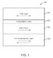
- FIG. 1shows the relevant layers of a magnetic tunnel junction of a magnetic memory element.
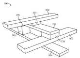
- FIG. 2shows a three-dimensional perspective view of magnetic memory element 200 .
- FIG. 3shows a three-dimensional perspective view of the magnetic memory element of FIG. 2 , being read by electron current 303 passed from the left electrode 206 to the magnetic tunnel junction 222 .
- FIG. 4shows a three-dimensional perspective view of the magnetic memory element of FIG. 2 , being written by electron current 401 passed from the left electrode 206 to the right electrode 232 .
- FIG. 5shows a three-dimensional perspective view of the magnetic memory element of FIG. 2 , being read by electron current 501 passed from the left electrode 206 to the magnetic tunnel junction 222 .
- FIG. 6shows a three-dimensional perspective view of the magnetic memory element of FIG. 2 , being written by electron current 601 passed from the right electrode 232 to the left electrode 206 .
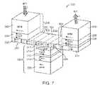
- FIG. 7shows a three-dimensional perspective view of the magnetic memory element of FIG. 2 , capable of multi-level storage by inducing multiple domain wall pinning sites.
- FIG. 8shows a top view of a notched free layer, capable of multi-level storage due to multiple domain wall pinning sites.
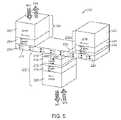
- FIG. 9shows a three-dimensional perspective view of a magnetic memory element arranged with respect to word line and bit line in a memory array assembly.
- FIG. 10shows a three-dimensional perspective view of an alternative magnetic memory element arrangement with respect to the bit lines and word line in a memory array assembly.
- FIG. 11shows the electron flow, through a magnetic memory element array assembly, for reading the state of a magnetic memory element.
- FIG. 12shows the electron flow, through a magnetic memory element array assembly, for writing a ‘0’ state to a magnetic memory element.
- FIG. 13shows the electron flow, through a magnetic memory element array assembly, for writing a ‘1’ state to a magnetic memory element.
- a magnetic tunnel junctionis located central to a free layer, with the free layer having stacks with pinned magnetic moments on either end, and the end-defining stacks creating a well defined magnetic domain state of the free layer therebetween.
- Pushing the free layer's domain wall towards either stackmodifies the domain state of the free layer.
- the domain wallis pushed by the passage of electron current from a stack, laterally through the free layer, to the other stack. As electron current flows laterally through the free layer, the domain wall is pushed in the direction of the electron flow due to spin transfer torque that exists between the polarized electron spin and the magnetic spins in the domain wall which are not aligned with the electron spins.
- the domain wallcan be pushed towards either stack. As a result, the domain wall can be dynamically positioned along the free layer between the stacks.
- a MTJLocated on a lateral face of the connecting free layer region is a MTJ.
- the domain wallcan be positioned within the free layer on either side of the MTJ, or anywhere therebetween.
- currentcan be passed from a stack, through the free layer, to the MTJ; or from the MTJ, through the free layer, to a stack.
- the MTJ's resistance to electron flowis a function of the domain wall's position within the free layer, and relative to the MTJ. Consequently, the MTJ's resistance to current allows for an accurate measurement of the domain wall's position, and thus allows for storage of a bit (by positioning of the domain wall), and reading of that bit (by reading the MTJ's resistance).
- a key to the present inventionis the creation of a well-defined domain wall by pinning magnetic moments at either end of the free layer.
- a fixed layer, pinned by an anti-ferromagnetic layeris located each end of the free layer.
- One of these fixed layerspins the spins of the free layer in a first direction, and the other fixed layer pins the spins of the free layer at the other end in a second, the opposite, direction. This is shown in FIGS. 2-7 , and discussed in further detail below.
- Stack 100is comprises an anti-ferromagnetic layer (AFM layer) 106 , a fixed layer 104 , a tunnel barrier layer 102 , and a free layer 101 .
- Stack 100is manufactured in such a manner that fixed layer 104 is formed upon AFM layer 106 , tunnel barrier layer 102 is formed upon fixed layer 104 , and free layer 101 is formed upon tunnel barrier layer 102 .
- Free layer 101 , tunnel barrier layer 102 , fixed layer 104 , and AFM layer 106are formed directly upon each other with no intermediate layers, and share the same width and depth of less than 500 nm, but mainly limited by the lithography technology being used to pattern the stack.
- Free layer 101has a thickness of about 2.5-3 nm; tunnel barrier layer has a thickness of about 1.25 nm; fixed layer 104 has a thickness of about 2.5 nm; and AFM layer 106 has a thickness of about 7 nm.
- the composition of AFM layer 106is typically alloys of IrMn or PtMn.
- Fixed layer 104is a compound of Co, Fe, and may contain one or more of the elements from the following list: B, P, Ni, Cr, Ta, Zr, Si, Cr, Mo, Hf, and/or W.
- the composition of tunnel barrier layer 102is chosen from: TiO 2, Al 2 O 3 , MgO, Ta 2 O 5 , HfO 2 , ZrO 2 , TaN, SrO, RuO, and ZnO; and is preferably MgO, or MgO combined with less than 50 molar % of any of the previously listed compounds.
- Free layer 101is preferably made of magnetic materials which have weakly exchange coupled grains; such as one, or more than one, of ferromagnetic elements Co, Fe, and Ni, and contains less than 20 atomic % of platinum (Pt). Free layer 101 may also contain up to 20 atomic % of one or more of: P, B, Cr, Ta, W, Mo, Zr, and/or Hf.
- AFM layer 106 , fixed layer 104 , tunnel barrier layer 102 , and free layer 101are formed using the same processes used to form the anti-ferromagnetic (AFM) layer, fixed layer, tunnel barrier layer, and free layer, respectively, of U.S. patent application Ser. No.
- Fixed layer 104has a magnetic moment direction pinned into a single direction through exchange coupling to adjacent AFM layer 106 .
- the magnetic moment direction of free layer 101can be changed between the parallel and anti-parallel direction with respect to fixed layer 104 .
- Tunnel barrier layer 102allows electrons to tunnel between fixed layer 104 and free layer 101 .
- free layer 101 's magnetic momentis parallel with fixed layer 104 's magnetic moment, the resistance to electron flow through tunnel barrier layer 102 is lower; and when free layer 101 's magnetic moment is anti-parallel with fixed layer 104 's magnetic moment, the resistance to electron flow through tunnel barrier layer 102 is higher.
- This difference in resistanceis also known as “tunnel magneto-resistance” or TMR.
- the magnetic moments' of the fixed layers of the present inventionare set using a magnetic annealing process whereby the magnetic films are exposed to a magnetic field of 4-10 kOe, applied in-plane of the wafer surface, at a temperature usually over 350° C.
- a magnetic field of 10 kOeis applied, in-plane of the wafer surface, at 360° C. for 2 hours.
- the field exposure timemay be shorter, for as short as a few minutes, or longer.
- the annealing processcauses re-crystallization of the free and fixed layers adjacent to the MgO tunnel barrier layer. This step is critical, as it ensures a high TMR, and impacts the read-speed of the final memory.
- Magnetic memory element 200is comprised generally to have a free layer 210 , having stacks 206 and 232 positioned on opposite ends of a lateral surface of free layer 210 , and MTJ 222 positioned centrally on a lateral surface of free layer 210 .
- stacks 206 and 232are shown positioned on a top surface, while MTJ 222 is positioned on a bottom surface of magnetic memory element 200 .
- Stacks 206 , 232 , MTJ 222 , and free layer 210all have substantially the same depth, less than 500 nm, but mainly limited by the lithography technology being used to pattern the stack.
- one or both stacksare positioned on the same free layer 210 surface as MTJ 222 is. This would be the bottom surface of free layer 210 in FIGS. 2-7 .
- stacks 206 and/or 232could extend from the same surface of free layer 210 , or from opposite surfaces of each other.
- stack 206might extend from the top surface of free layer 210 while MTJ 222 and stack 232 extend from the bottom surface of free layer 210 ; or both stacks 206 and 232 extend from the bottom surface with MTJ 222 .
- top surfaceor a “bottom surface” of free layer 210 is used strictly in reference to drawings, to assist in orientation, and “surfaces” refers to the flat lateral sides of free layer 210 with the greatest surface area.
- the top surfaceis so called because it is closer to the top of the page as viewed in FIGS. 2-7 , while the bottom surface of free layer 210 , hidden underneath and not visible due to the perspective view, is closer to the bottom of the page.
- Stack 206comprises AFM layer 202 formed upon fixed layer 204 , and fixed layer 204 is formed upon free layer 210 .
- the layers of stack 206have substantially the same depth and width, forming a generally uniform raised structure.
- Stack 232comprises AFM layer 230 formed upon fixed layer 228 , which is formed upon spacer layer 226 , and spacer layer 226 is formed upon free layer 210 .
- the layers of stack 232have substantially the same depth and width, forming a generally uniform raised structure.
- AFM layers 202 and 230pin the directions of the magnetic moments of fixed layers 204 and 228 , respectively.
- AFM layers 202 and 230are formed by the same process, and share the same properties, as AFM layer 106 .
- Fixed layers 204 and 228are formed by the same process, and share the same properties, as fixed layer 104 .
- Spacer layer 226comprises a thin layer of Ru, typically 0.8-1 nm thick. Spacer layer 226 reverses the effective magnetic exchange coupling between fixed layer 228 to free layer 210 .
- the magnetic annealing of a waferis a global process affecting the whole wafer, aligning the magnetic moments of all of the AFM layers ( 202 , 230 , and 220 ), and consequently pinning the magnetic moments of fixed layers adjacent to the AFM layers—fixed layers 204 , 226 , and 218 , respectively—in the same direction.
- the magnetic moments of stacks at each end of free layer 210should have magnetic moments anti-parallel to each other.
- Free layer 210is shown to have two domains, anti-parallel domain 208 and parallel domain 224 , anti-parallel domain 208 and parallel domain 224 being separated by domain wall 235 .
- Domain wall 235is an interface or transition between the parallel magnetic field of parallel domain 224 and the anti-parallel magnetic field of anti-parallel domain 208 .
- Parallel and anti-parallelare used in reference to MTJ 222 .
- the magnetic moment of parallel domain 224is designated by arrows pointing to the right, in the same direction as the magnetic moment of fixed layer 214 of MTJ 222 .
- Anti-parallel domain 208 's magnetic momentis designated by arrows pointing to the left, which is anti-parallel to the magnetic moment of fixed layer 214 of MTJ 222 .
- Domain wall 235spans a distance of about 100-150 atoms.
- the free layersare referred to and depicted as being rectangular, with four flat lateral sides and 2 flat ends. Further, two of the lateral sides are depicted as having significantly greater surface area than the other two lateral sides, the two lateral sides with the greater surface area being referred to as the “top surface and “bottom” surface of the free layers.
- This thin, flat, but deep conformationlends itself to a simplified manufacturing process, reduces the cross-sectional area, and better defines the free layer's domain wall, but other conformations are considered.
- Other conformationsmay include a free layer having four lateral sides of all the same size (square extruded), or triangular extruded, or any other geometric shape where a well-defined domain wall can be maintained within.
- MTJ 222is formed on a lateral surface of free layer 210 , substantially central to the surface, and may be on a lateral side opposite of stacks 206 and 232 , and.
- MTJ 222comprises a tunnel barrier layer 212 , fixed layers 214 and 218 , spacer layer 216 , and AFM layer 220 .
- MTJ 222is formed upon the lateral surface of free layer 210 , upon which is formed fixed layer 214 , upon which is formed spacer layer 216 , upon which is formed fixed layer 218 , and upon which is formed AFM layer 220 .
- the two fixed layers 214 and 218have opposite magnetic moments (also known as a “synthetic anti-ferromagnet) which reduces the magneto-static interaction between the fixed layers and free layer 210 .
- the MTJ 222have substantially the same depth and width, forming a generally uniform raised structure off of a free layer 210 lateral surface.
- Free layer 210is made of weakly exchange coupled magnetic materials. This allows for the magnetic domains 208 and 224 to be more easily shrunken and enlarged. Free layer 210 carries the spin transfer current from stack-to-stack, or stack-to-MTJ. The cross sectional area of free layer 210 can be made very small, especially compared to the lateral dimensions of the free layer 210 or the MTJ 222 , making domain wall 235 amenable to movement by the passage of a low current.
- Tunnel barrier layer 212is a non-conducting crystalline layer that allows the passage of electrons from free layer 210 to fixed layer 214 , or in the opposite direction, from fixed layer 214 to free layer 210 through tunneling. Tunnel barrier layer 212 is identical to tunnel barrier layer 102 in function, composition, and thickness, as described in detail above.
- domain wall 235is closer to stack 206 (located within free layer 210 between stack 206 and MTJ 222 ), and thus parallel domain 224 of free layer 210 is adjacent to tunnel barrier layer 212 .
- parallel domain 224 's magnetic momentis anti-parallel to the magnetic moments of fixed layers 204 and 228 , but is parallel to that of fixed layer 214 .
- the conducting spacer layer 216is identical to spacer layer 226 in function, and possible composition and thickness, as described above in detail. Spacer layer 216 is located in between fixed layers 218 and 214 and inverts the magnetic exchange coupling between fixed layers 218 and 214 . Consequently, the magnetic moment of fixed layer 214 is anti-parallel to the magnetic moments of all other fixed layers ( 204 , 228 , 218 ) in magnetic memory element 200 .
- the magnetic state of magnetic memory element 200is being read.
- the magnetic state of memory element 200is read by passing either current 303 or current 301 through magnetic memory element 200 .
- Current 303is applied at AFM layer 202 of stack 206 , passes through stack 206 , into and laterally through free layer 210 , and then out MTJ 222 through AFM layer 220 .
- Current 301is applied at AFM layer 220 of MTJ 222 , passes through MTJ 222 , into and through free layer 210 , and then out of stack 206 through AFM layer 202 .
- domain wall 235When domain wall 235 is positioned such that parallel domain 224 is adjacent to tunnel barrier layer 212 , the electron spin orientations in free layer 210 and fixed layer 214 are parallel, and currents 301 and/or 303 experience a low resistance state.
- the magnetic state of memory element 200can be read by passing the current through stack 232 instead of stack 206 .
- Electron current 401is applied at AFM layer 202 of stack 206 , passes through stack 206 , into and laterally through free layer 210 , and then out of stack 232 through AFM layer 230 . As electron current 401 passed through free layer 401 , it pushes domain wall 404 to the right, towards stack 232 . Domain wall 404 , as shown, is one possible position of the domain wall within free layer 210 as it is pushed from stack 206 , towards stack 232 , and is a repositioned domain wall 235 .
- FIG. 5the memory state of magnetic memory element 200 is again being read.
- current passed from stack 206 to stack 232(shown in FIG. 4 as current 401 ) has moved domain wall 504 to the other side of MTJ 222 .
- domain wall 504is between MTJ 222 and stack 232 , and anti-parallel domain 208 of free layer 210 is now adjacent to, and interfaced with, tunnel barrier layer 212 .
- current 501 or current 503is passed through magnetic memory element 200 .
- Current 501is applied to AFM layer 202 of stack 206 , passes through stack 206 , into and laterally through free layer 210 , and then through MTJ 222 , out through AFM layer 220 .
- Current 503is applied to AFM layer 220 of MTJ 222 , passes through MTJ 222 , into and laterally through free layer 210 , and then through stack 206 , out through AFM layer 202 .
- the magnetic state of memory element 200can be read by passing the current through stack 232 instead of stack 206 .
- domain wall 504When domain wall 504 is positioned so that anti-parallel domain 208 is adjacent to tunnel barrier layer 212 , the magnetic spin orientations of adjacent free layer 210 and neighboring fixed layer 214 are anti-parallel, and currents 501 and/or 503 experience a high resistance state.
- This high resistance stateexperienced by currents 501 and 503 when passing from anti-parallel domain 208 through tunnel barrier layer 212 to fixed layer 214 , is higher than the resistance experienced by currents 301 and 303 when passing through parallel domain 224 , tunnel barrier layer 212 , and fixed layer 214 . Because these different resistance states are a direct function of the positioning of the domain wall (domain walls 235 and 504 within FIGS. 2-5 ), the domain wall positioning effectively represents either a ‘0’ or a ‘1’ state of magnetic memory element 200 .
- Electron current 601is applied at AFM layer 230 of stack 232 , passes through stack 232 , into and laterally through free layer 210 , and then out of stack 206 through AFM layer 202 . Electron current 601 pushes domain wall 604 to the left, towards stack 206 .
- Domain wall 604is one possible position of the domain wall within free layer 210 as it is pushed from stack 232 , towards stack 206 . Eventually, domain wall 604 will be returned to domain wall 235 in the position shown in FIG. 2 , and consequently magnetic memory element 200 will be returned to the associated state.
- the currents 301 , 303 , 501 and 503typically have a much smaller magnitude than the current 401 and 601 .
- the magnitude of currents 301 , 303 , 501 , and 503is reduced in order to prevent domain wall motion during the read out process.
- memory element 200may be capable of storing more than 2 memory states, i.e., more than just ‘0’ or ‘1’. This is possible by using electron currents 401 and 601 to relocate the domain wall of free layer 410 to more than two positions.
- the domain wall within free layer 410may be positioned where domain walls 404 and 604 are depicted positioned previously, as well as other positions.
- domain walls 404 and 604are positioned such that tunnel barrier layer is adjacent to areas of anti-parallel domain 208 and parallel domain 224 concurrently.
- This sub-division of memory statesis possible by applying an electron pulse (current) that pushes the domain wall only a limited distance. When the domain wall is in these intermediate positions, resistance values between the previously described high resistance and low resistance states are obtained.
- domain wall 404is positioned in a manner that makes a larger area of parallel domain 224 adjacent/interfaced to tunnel barrier layer 212 than anti-parallel domain 208 .
- Domain wall 704is positioned in a manner that makes equal areas of anti-parallel domain 208 and parallel domain 224 adjacent/interfaced to tunnel barrier layer 212 .
- Domain wall 604is positioned in a manner that makes a larger area of anti-parallel domain 208 adjacent/interfaced to tunnel barrier layer 212 than parallel domain 224 .
- the resistance of MTJ 222is a function of the surface areas of parallel domain 224 and of anti-parallel domain 208 that are interfaced with tunnel barrier layer 212 .
- the resistance to currentdecreases as tunnel barrier layer 212 is interfaced with a greater surface area of parallel domain 224 , and lesser area of anti-parallel domain 208 .
- the resistance to currentincreases as tunnel barrier layer 212 is interfaced with a greater surface area of anti-parallel domain 208 , and lesser area of parallel domain 224 .
- a read operation of magnetic memory element 200 with domain wall 404would experience less resistance than a read operation of magnetic memory element 200 with domain wall 704 .
- a read operation of magnetic memory element 200 with domain wall 604would have a greater resistance than domain walls 404 or 704 . All of these resistance values would be between the high resistance state (domain wall 235 ) and low resistance state (domain wall 504 ), shown in FIGS. 2 and 5 respectively.
- FIG. 8another method of achieving multiple levels of memory states is shown, in an alternative embodiment of the present invention.
- a top view of free layer 810 of magnetic memory element 800is shown.
- MTJMagnetic MTJ
- MTJ 818Central to the bottom surface of free layer 810 , hidden below notch region 811 and not visible in FIG. 8 , is an MTJ, MTJ 818 , comprised of the same layers as MTJ 222 of magnetic memory element 200 .
- the notches 812 , 814 , and 816 in free layer 810all correspond to a preferred domain wall position.
- the cross-sectional area of free layer 810is at a minimum, and thus the domain wall thickness is reduced, and better defined.
- each notch positionis associated with a different resistance, with resistance increasing as a larger region of anti-parallel magnetic domain interfaces with the tunnel barrier layer of MTJ 818 . This creates an effective way to “lock” the domain wall in consistent positions, and thus makes multi-level storage more reliable.
- Magnetic memory arrayincludes magnetic memory element 200 , with MTJ 222 , free layer 210 , and stacks 232 and 206 labeled appropriately.
- bit line read 902is coupled; on AFM layer 230 of stack 232 , bit line write 903 is coupled; and on AFM layer 202 of stack 206 , pinning layer 905 is coupled, which has word line read/write formed thereupon.
- Magnetic memory element 200is inverted, with respect to how it is shown in FIGS. 2-7 , so that MTJ 222 extends upward from free layer 210 , and stacks 232 and 206 extend downward from free layer 210 . Consequently, MTJ 222 is the top-most part of magnetic memory element 200 , and bit line read 902 , above MTJ 222 , is the highest line.
- Bit line read 902is parallel to bit line write 903 .
- Bit line write 903runs below memory element 200 , perpendicular to the lengthwise direction of free layer 210 .
- Pinning layer 906is formed off of AFM layer 230 , and pinning layer 906 extends downward, coupled to word line read/write 904 .
- the pinning layer 906has the same function as pinning layer 204 in FIGS. 2-7 .
- Word line read/write 904runs parallel to free layer 210 , below bit line write 903 , and at a distance of the height of pinning layer 905 plus the height of stack 206 .
- An important feature of array 900is that bit line read 902 and bit line write 903 are in different planes.
- Bit line read 902is connected to MTJ 222 , as current is only passed through it to read the memory state of the memory element; bit line write 903 is connected to stack 232 , as current passes through it only to write the memory state of the memory element; and word line read/write 904 is connected to stack 206 , as current passes through it for both reading and writing the memory state of the memory element.
- FIG. 9to simplify the drawing, only one magnetic memory element is included in array 900 , but in practice many magnetic memory elements may be attached to word line read/write 904 , bit line write 903 , and bit line read 902 .
- This direct connectioncan be modified to include a select transistor.
- the word lineis connected to the gate of the transistor, the left side fixed layer is connected to one end of the transistor, and the other end of the transistor can be at low (e.g. ground) or high potential, depending on the direction of the read current and the direction of the write current.
- FIG. 10a three-dimensional perspective view of magnetic memory array 1000 is shown in an alternative embodiment of the present invention.
- the bit line arrangement and the memory elementare configured differently than with memory element 200 or array 900 .
- bit line read 1002 and bit line write 1003are parallel to each other and in the same plane.
- the magnetic memory element of array 1000is configured in a manner so that MTJ 1022 and stack 1032 extend off of the same (top) surface of free layer 1010 , and stack 1006 extends off of the other (bottom) surface of free layer 1010 .
- Stack 1006is structurally and functionally identical to stack 206
- free layer 1010is structurally and functionally identical to free layer 210
- MTJ 1022is structurally and functionally identical to MTJ 222
- stack 1032is structurally and functionally identical to stack 232 .
- the relocation of one of the stacks, stack 1032 , to the same surface of free layer 1010 as the MTJ, MTJ 1022does not cause the magnetic memory element to operate any differently than as discussed above for memory element 200 .
- bit line read 1002 and bit line write 1003are the top most components, with word line read/write 1004 the bottom most component, and the magnetic memory element sandwiched between.
- This alternative orientationprovides an alternative method of laying out the magnetic memory circuitry.
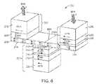
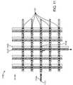
- array 1100is shown consisting of 25 (twenty-five) magnetic memory elements 1101 , each having two stacks and an MTJ, and all connected to a word line read/write, bit line read, and bit line write.
- magnetic memory element 1108is connected to word line read/write 1104 at one stack, bit line write 1103 at a second stack, and bit line read 1102 at its MTJ.
- current 1111is applied to word line read/write 1104 , which travels through magnetic memory element 1108 , and out through bit line read 1102 . Because word line read/write 1104 is connected to magnetic memory element 1108 at a stack, e.g. stack 206 or 1006 , and bit line read 1102 is connected to magnetic memory element 1108 's MTJ, e.g., MTJ 222 or 1022 , application of current 1111 will provide a resistance value for reading the memory state of magnetic memory element 1108 .
- current 1211is applied to word line read/write 1104 , which travels through magnetic memory element 1108 , and out through bit line write 1103 .
- word line read/write 1104is connected to magnetic memory element 1108 at one stack, e.g. stack 206 or 1006
- bit line write 1103is connected at magnetic memory element 1108 's second stack, e.g. stack 232 or 1032
- application of 1211pushes the domain wall within magnetic memory element 1108 's free layer towards the second stack connected to bit line write 1103 , and writes a ‘0’ value to the magnetic memory element.
- current 1311is applied to bit line write 1103 , which travels through magnetic memory element 1108 , and out through word line read/write 1104 .
- Current 1311pushes the domain wall of magnetic memory element 1108 in a direction opposite to how it's pushed by current 1211 , towards the first stack connected to word line read/write 1104 , and consequently a ‘1’ value is written to magnetic memory element 1108 .
- HDLhardware description language
- Applicable HDLsinclude those at the layout, circuit netlist, and/or schematic capture levels. Examples of HDLs include, but are not limited to: GDS II and OASIS (layout level); various SPICE languages, and IBIS (circuit netlist level); and Virtuoso custom design language and Design Architecture-IC custom design language (schematic capture level). HDL descriptions may also be used for a variety of purposes, including but not limited to layout, behavior, logic and circuit design verification, modeling, and/or simulation.
Landscapes
- Engineering & Computer Science (AREA)
- Computer Hardware Design (AREA)
- Hall/Mr Elements (AREA)
- Mram Or Spin Memory Techniques (AREA)
Abstract
Description
- This application claims benefit of U.S. Provisional Patent Application, entitled “Low Current Switching Magnetic Tunnel Junction Design for Magnetic Memory using Domain Wall Motion,” U.S. Provisional Application No. 61/001,348, filed on Oct. 31, 2007, and from U.S. patent application Ser. No. 11/674,124, entitled “Non-Uniform Switching Based Non-Volatile Magnetic Base Memory,” filed Feb. 12, 2007, by Ranjan, et al., U.S. patent application Ser. No. 11/678,515, entitled “A High Capacity Low Cost Multi-State Magnetic Memory,” filed Aug. 23, 2008, by Ranjan, et al., U.S. patent application Ser. No. 11/776,692, entitled “Non-Volatile Magnetic Memory Element with Graded Layer,” filed Jul. 12, 2007, by Ranjan, et al., U.S. patent application Ser. No. 11/740,861, entitled “High Capacity Low Cost Multi-Stacked Cross-Line Magnetic Memory,” filed Apr. 26, 2007, by Ranjan, et al., and U.S. Provisional Patent Application No. 61/045,582, entitled “Low Power Non-Volatile Magnetic Memory Design,” filed Apr. 16, 2008, by Ranjan, et al.
- 1. Field of the Invention
- The present invention relates to a novel low-current multi-state current-switching magnetic memory, and, more specifically, to a magnetic memory element employing the torque generated by the polarized spins of electrons to move a free layer domain wall relative to a magnetic tunnel junction.
- 2. Description of the Prior Art
- Computers conventionally use rotating magnetic media for data storage in the form of magnetic hard disk drives (HDDs). Though widely used and commonly accepted, such hard disk drives suffer from a variety of deficiencies. Access latency, higher power dissipation, increased physical size and inability to withstand any physical shock justifies a new type of storage device. Other dominant semiconductor based storage devices are DRAM and SRAM which are volatile and very costly, but have faster random read/write time. Solid-state-nonvolatile-memory (SSNVM) devices like NOR/NAND flash memory provide higher access time, higher IOP speed, lower power dissipation, smaller physical size, and higher reliability, but at a cost which tends to be generally multiple times higher than HDDs.
- Although NAND flash memory is more costly, it has replaced HDDs in many applications such as digital cameras, MP3 players, cell phones, and hand held multimedia devices. However, as process geometry is getting smaller, the design of NAND flash memory and DRAM memory is becoming more difficult to scale. For example, NAND flash memory has issues related to capacitive coupling, few electrons/bit, poor error-rate performance, and poor reliability due to low read-write endurance. It is believed that NAND flash memory, especially multi-bit designs will be extremely difficult to scale below 45 nm-lithography. Likewise, DRAM has issues related to scaling trench capacitors, necessitating complex designs that are becoming difficult to manufacture, and leading to higher costs.
- Currently many platforms use combinations of EEPROM/NOR, NAND, HDDs, and DRAM as a part of the system design. Use of multiple memory technologies in a single product will add to the design complexity, time to market, and the final cost. For example, a handheld multi-media device which incorporates NAND Flash, DRAM, and EEPROM/NOR flash will have additional levels of design complexity, cost more, and take longer to reach the market than a device incorporating fewer unique memory technologies. Also, incorporating multiple memory technologies increases the device's footprint, an undesirable property for a handheld device.
- There has also been extensive effort in development of alternative technologies such as Ovanic RAM (or phase-change memory), Ferro-electric RAM (FeRAM), Magnetic RAM (MRAM), nanochip, and others, to replace memories used in current designs. Although these various memory/storage technologies have created many challenges, there have been great advances made in this field in recent years. Magnetic-random-access-memory (MRAM) seems to lead as the best candidate to replace all types of memories as a universal memory solution. Recently, low capacity MRAM, which relies on a magnetic field to switch the memory elements, started shipping. Numerous scientific papers have shown that direct electrical current can also be used to switch the memory elements. There is a tradeoff between low-switching current, and reliability of the memory associated due to thermal stability.
- The current-switching tradeoff arises due to the interaction between magnetic moments and the electrical transport current. At least two dominant mechanisms have been proposed, namely, (1) current induced magnetic field and, (2) spin-torque from the current spin polarization. While the current induced effect through the magnetic field is directly proportion to radius (r), the later spin-torque effect is proportional to r2, where r is the distance from the center of current carrying device. Incidentally, the torque generated by spins through the momentum transfer of tunneled polarized spins from the fixed layer, which opposes the “intrinsic” damping of spins of the free-layer. At sufficient current this can reverse the direction of the magnetization in the free layer. The critical current required for such switching:
- Where Ic0is the critical switching current density without thermal fluctuation; kbis the Boltzman constant; T is the temperature; Kuis the effective uniaxial anisotropy; V is the volume of the free-layer; t0is the inverse of the procession frequency of the spin (less than 1 ns); tpis the pulse width of the switching current.
Equation 1 shows that one way to reduce the critical switching current density is by reducing either Ku or V of the free-layer. Secondly, the switching current can be reduced by utilizing a thinner free-layer, but this may compromise reliability by making the memory cell thermally unstable. A memory element with a free-layer having a higher KuV is more thermally stable at higher temperatures. A general rule of thumb is that the magnetic energy, KuV, of the free-layer be greater than about 80 kbT where, kbis the Boltzmann constant and T is the ambient temperature.- What is needed is a novel memory that has high tunneling magneto-resistance (TMR) while having flexibility in the selection of resistance-area product (RA) and lateral dimensions of the magnetic tunnel junction. A high TMR is highly desirable as it enables high easier sensing between the two states, while flexibility in RA design with lateral size enables scalability, as well as improving reliability.
- Briefly, a multi-state low-current-switching magnetic memory element (magnetic memory element) using domain wall positioning to define the memory state is disclosed. The magnetic memory element comprises a substantially flat, elongated free layer, with stacks disposed on each end. The stacks serve both as electrodes, and, due to each having a unique magnetic moment, pin each end of the free layer in opposite magnetic directions. The pinned magnetic moments generate a well-defined domain wall within the free layer. Disposed central to the free layer is a magnetic tunnel junction (MTJ). Current may be passed between the stacks, in either direction, to push the free layer's domain wall in the same direction as electron current is passed, and relocates the domain wall accordingly. Current may also be passed between a stack and the MTJ, providing a resistance value reading. The resistance value is dependent upon the location of the domain wall relative to the MTJ, therefore allowing the magnetic memory element to “store” various values, dependent upon its magnetic state.
- These and other objects and advantages of the present invention will no doubt become apparent to those skilled in the art after having read the following detailed description of the preferred embodiments illustrated in the several figures of the drawing.
FIG. 1 shows the relevant layers of a magnetic tunnel junction of a magnetic memory element.FIG. 2 shows a three-dimensional perspective view ofmagnetic memory element 200.FIG. 3 shows a three-dimensional perspective view of the magnetic memory element ofFIG. 2 , being read byelectron current 303 passed from theleft electrode 206 to themagnetic tunnel junction 222.FIG. 4 shows a three-dimensional perspective view of the magnetic memory element ofFIG. 2 , being written byelectron current 401 passed from theleft electrode 206 to theright electrode 232.FIG. 5 shows a three-dimensional perspective view of the magnetic memory element ofFIG. 2 , being read byelectron current 501 passed from theleft electrode 206 to themagnetic tunnel junction 222.FIG. 6 shows a three-dimensional perspective view of the magnetic memory element ofFIG. 2 , being written byelectron current 601 passed from theright electrode 232 to theleft electrode 206.FIG. 7 shows a three-dimensional perspective view of the magnetic memory element ofFIG. 2 , capable of multi-level storage by inducing multiple domain wall pinning sites.FIG. 8 shows a top view of a notched free layer, capable of multi-level storage due to multiple domain wall pinning sites.FIG. 9 shows a three-dimensional perspective view of a magnetic memory element arranged with respect to word line and bit line in a memory array assembly.FIG. 10 shows a three-dimensional perspective view of an alternative magnetic memory element arrangement with respect to the bit lines and word line in a memory array assembly.FIG. 11 shows the electron flow, through a magnetic memory element array assembly, for reading the state of a magnetic memory element.FIG. 12 shows the electron flow, through a magnetic memory element array assembly, for writing a ‘0’ state to a magnetic memory element.FIG. 13 shows the electron flow, through a magnetic memory element array assembly, for writing a ‘1’ state to a magnetic memory element.- In the following description of the embodiments, reference is made to the accompanying drawings that form a part hereof, and in which is shown by way of illustration of the specific embodiments in which the invention may be practiced. It is to be understood that other embodiments may be utilized because structural changes may be made without departing from the scope of the present invention. It should be noted that the figures discussed herein are not drawn to scale and thicknesses of lines are not indicative of actual sizes.
- In an embodiment of the present invention a magnetic tunnel junction (MTJ) is located central to a free layer, with the free layer having stacks with pinned magnetic moments on either end, and the end-defining stacks creating a well defined magnetic domain state of the free layer therebetween. Pushing the free layer's domain wall towards either stack modifies the domain state of the free layer. The domain wall is pushed by the passage of electron current from a stack, laterally through the free layer, to the other stack. As electron current flows laterally through the free layer, the domain wall is pushed in the direction of the electron flow due to spin transfer torque that exists between the polarized electron spin and the magnetic spins in the domain wall which are not aligned with the electron spins.
- Depending on the direction in which electron current is applied, the domain wall can be pushed towards either stack. As a result, the domain wall can be dynamically positioned along the free layer between the stacks. Located on a lateral face of the connecting free layer region is a MTJ. The domain wall can be positioned within the free layer on either side of the MTJ, or anywhere therebetween. In addition to passing current from stack to stack, current can be passed from a stack, through the free layer, to the MTJ; or from the MTJ, through the free layer, to a stack. The MTJ's resistance to electron flow is a function of the domain wall's position within the free layer, and relative to the MTJ. Consequently, the MTJ's resistance to current allows for an accurate measurement of the domain wall's position, and thus allows for storage of a bit (by positioning of the domain wall), and reading of that bit (by reading the MTJ's resistance).
- A key to the present invention is the creation of a well-defined domain wall by pinning magnetic moments at either end of the free layer. In one embodiment of the present invention a fixed layer, pinned by an anti-ferromagnetic layer, is located each end of the free layer. One of these fixed layers pins the spins of the free layer in a first direction, and the other fixed layer pins the spins of the free layer at the other end in a second, the opposite, direction. This is shown in
FIGS. 2-7 , and discussed in further detail below. - Referring now to
FIG. 1 , stack100 is shown.Stack 100 is comprises an anti-ferromagnetic layer (AFM layer)106, a fixedlayer 104, atunnel barrier layer 102, and afree layer 101.Stack 100 is manufactured in such a manner that fixedlayer 104 is formed uponAFM layer 106,tunnel barrier layer 102 is formed upon fixedlayer 104, andfree layer 101 is formed upontunnel barrier layer 102.Free layer 101,tunnel barrier layer 102, fixedlayer 104, andAFM layer 106 are formed directly upon each other with no intermediate layers, and share the same width and depth of less than 500 nm, but mainly limited by the lithography technology being used to pattern the stack.Free layer 101 has a thickness of about 2.5-3 nm; tunnel barrier layer has a thickness of about 1.25 nm; fixedlayer 104 has a thickness of about 2.5 nm; andAFM layer 106 has a thickness of about 7 nm. - The composition of
AFM layer 106 is typically alloys of IrMn or PtMn.Fixed layer 104 is a compound of Co, Fe, and may contain one or more of the elements from the following list: B, P, Ni, Cr, Ta, Zr, Si, Cr, Mo, Hf, and/or W. The composition oftunnel barrier layer 102 is chosen from: TiO2, Al2O3, MgO, Ta2O5, HfO2, ZrO2, TaN, SrO, RuO, and ZnO; and is preferably MgO, or MgO combined with less than 50 molar % of any of the previously listed compounds.Free layer 101 is preferably made of magnetic materials which have weakly exchange coupled grains; such as one, or more than one, of ferromagnetic elements Co, Fe, and Ni, and contains less than 20 atomic % of platinum (Pt).Free layer 101 may also contain up to 20 atomic % of one or more of: P, B, Cr, Ta, W, Mo, Zr, and/or Hf.AFM layer 106, fixedlayer 104,tunnel barrier layer 102, andfree layer 101 are formed using the same processes used to form the anti-ferromagnetic (AFM) layer, fixed layer, tunnel barrier layer, and free layer, respectively, of U.S. patent application Ser. No. 11/674,124, entitled “Non-Uniform Switching Based Non-Volatile Magnetic Base Memory,” filed Feb. 12, 2007, by Ranjan, et al.; U.S. patent application Ser. No. 11/678,515, entitled “A High Capacity Low Cost Multi-State Magnetic Memory,” filed Aug. 23, 2008, by Ranjan, et al.; U.S. patent application Ser. No. 11/776,692, entitled “Non-Volatile Magnetic Memory Element with Graded Layer,” filed Jul. 12, 2007, by Ranjan, et al.; U.S. patent application Ser. No. 11/740,861, entitled “High Capacity Low Cost Multi-Stacked Cross-Line Magnetic Memory,” filed Apr. 26, 2007, by Ranjan, et al.; and U.S. Provisional Patent Application No. 61/045,582, entitled “Low Power Non-Volatile Magnetic Memory Design,” filed Apr. 16, 2008, by Ranjan, et al. Fixed layer 104 has a magnetic moment direction pinned into a single direction through exchange coupling toadjacent AFM layer 106. The magnetic moment direction offree layer 101 can be changed between the parallel and anti-parallel direction with respect to fixedlayer 104.Tunnel barrier layer 102 allows electrons to tunnel between fixedlayer 104 andfree layer 101. Whenfree layer 101's magnetic moment is parallel withfixed layer 104's magnetic moment, the resistance to electron flow throughtunnel barrier layer 102 is lower; and whenfree layer 101's magnetic moment is anti-parallel with fixedlayer 104's magnetic moment, the resistance to electron flow throughtunnel barrier layer 102 is higher. This difference in resistance is also known as “tunnel magneto-resistance” or TMR.- The magnetic moments' of the fixed layers of the present invention are set using a magnetic annealing process whereby the magnetic films are exposed to a magnetic field of 4-10 kOe, applied in-plane of the wafer surface, at a temperature usually over 350° C. In one embodiment of the present invention, a magnetic field of 10 kOe is applied, in-plane of the wafer surface, at 360° C. for 2 hours. In other embodiments of the present invention the field exposure time may be shorter, for as short as a few minutes, or longer. The annealing process causes re-crystallization of the free and fixed layers adjacent to the MgO tunnel barrier layer. This step is critical, as it ensures a high TMR, and impacts the read-speed of the final memory.
- Referring now to
FIG. 2 ,magnetic memory element 200 is shown.Magnetic memory element 200 is comprised generally to have afree layer 210, havingstacks free layer 210, andMTJ 222 positioned centrally on a lateral surface offree layer 210. InFIG. 2 ,stacks MTJ 222 is positioned on a bottom surface ofmagnetic memory element 200.Stacks MTJ 222, andfree layer 210 all have substantially the same depth, less than 500 nm, but mainly limited by the lithography technology being used to pattern the stack. - In an alternative embodiment of the present invention, one or both stacks are positioned on the same
free layer 210 surface asMTJ 222 is. This would be the bottom surface offree layer 210 inFIGS. 2-7 . Thus, stacks206 and/or232 could extend from the same surface offree layer 210, or from opposite surfaces of each other. For example, stack206 might extend from the top surface offree layer 210 whileMTJ 222 and stack232 extend from the bottom surface offree layer 210; or bothstacks MTJ 222. The reference to a “top surface” or a “bottom surface” offree layer 210 is used strictly in reference to drawings, to assist in orientation, and “surfaces” refers to the flat lateral sides offree layer 210 with the greatest surface area. The top surface is so called because it is closer to the top of the page as viewed inFIGS. 2-7 , while the bottom surface offree layer 210, hidden underneath and not visible due to the perspective view, is closer to the bottom of the page. Stack 206 comprisesAFM layer 202 formed upon fixedlayer 204, and fixedlayer 204 is formed uponfree layer 210. The layers ofstack 206 have substantially the same depth and width, forming a generally uniform raised structure.Stack 232 comprisesAFM layer 230 formed upon fixedlayer 228, which is formed uponspacer layer 226, andspacer layer 226 is formed uponfree layer 210. The layers ofstack 232 have substantially the same depth and width, forming a generally uniform raised structure.- AFM layers202 and230 pin the directions of the magnetic moments of fixed
layers AFM layer 106.Fixed layers layer 104.Spacer layer 226 comprises a thin layer of Ru, typically 0.8-1 nm thick.Spacer layer 226 reverses the effective magnetic exchange coupling between fixedlayer 228 tofree layer 210. This is necessary because the magnetic annealing of a wafer is a global process affecting the whole wafer, aligning the magnetic moments of all of the AFM layers (202,230, and220), and consequently pinning the magnetic moments of fixed layers adjacent to the AFM layers—fixedlayers domain wall 235 withinfree layer 210, the magnetic moments of stacks at each end of free layer210 (stacks 206 and232) should have magnetic moments anti-parallel to each other. Free layer 210 is shown to have two domains,anti-parallel domain 208 andparallel domain 224,anti-parallel domain 208 andparallel domain 224 being separated bydomain wall 235.Domain wall 235 is an interface or transition between the parallel magnetic field ofparallel domain 224 and the anti-parallel magnetic field ofanti-parallel domain 208. “Parallel” and “anti-parallel” are used in reference toMTJ 222. As shown inFIGS. 2-7 , the magnetic moment ofparallel domain 224 is designated by arrows pointing to the right, in the same direction as the magnetic moment of fixedlayer 214 ofMTJ 222.Anti-parallel domain 208's magnetic moment is designated by arrows pointing to the left, which is anti-parallel to the magnetic moment of fixedlayer 214 ofMTJ 222.Domain wall 235 spans a distance of about 100-150 atoms.- In the following disclosures and figures, the free layers (e.g. free layer210) are referred to and depicted as being rectangular, with four flat lateral sides and 2 flat ends. Further, two of the lateral sides are depicted as having significantly greater surface area than the other two lateral sides, the two lateral sides with the greater surface area being referred to as the “top surface and “bottom” surface of the free layers. This thin, flat, but deep conformation lends itself to a simplified manufacturing process, reduces the cross-sectional area, and better defines the free layer's domain wall, but other conformations are considered. Other conformations may include a free layer having four lateral sides of all the same size (square extruded), or triangular extruded, or any other geometric shape where a well-defined domain wall can be maintained within.
MTJ 222 is formed on a lateral surface offree layer 210, substantially central to the surface, and may be on a lateral side opposite ofstacks MTJ 222 comprises atunnel barrier layer 212, fixedlayers spacer layer 216, andAFM layer 220.MTJ 222 is formed upon the lateral surface offree layer 210, upon which is formed fixedlayer 214, upon which is formedspacer layer 216, upon which is formed fixedlayer 218, and upon which is formedAFM layer 220. The twofixed layers free layer 210. TheMTJ 222 have substantially the same depth and width, forming a generally uniform raised structure off of afree layer 210 lateral surface.Free layer 210 is made of weakly exchange coupled magnetic materials. This allows for themagnetic domains Free layer 210 carries the spin transfer current from stack-to-stack, or stack-to-MTJ. The cross sectional area offree layer 210 can be made very small, especially compared to the lateral dimensions of thefree layer 210 or theMTJ 222, makingdomain wall 235 amenable to movement by the passage of a low current.Tunnel barrier layer 212 is a non-conducting crystalline layer that allows the passage of electrons fromfree layer 210 to fixedlayer 214, or in the opposite direction, from fixedlayer 214 tofree layer 210 through tunneling.Tunnel barrier layer 212 is identical totunnel barrier layer 102 in function, composition, and thickness, as described in detail above.- In
FIG. 2 , as indicated by the arrows infree layer 210,domain wall 235 is closer to stack206 (located withinfree layer 210 betweenstack 206 and MTJ222), and thusparallel domain 224 offree layer 210 is adjacent totunnel barrier layer 212. As explained aboveparallel domain 224's magnetic moment is anti-parallel to the magnetic moments of fixedlayers layer 214. Whenparallel domain 224 offree layer 210 is located adjacent totunnel barrier layer 212 the resistance experienced by any current passing through to, or from,MTJ 222 is less than the resistance experienced whendomain wall 235 is pushed to the other side ofMTJ 222, andanti-parallel domain 208 is located adjacent totunnel barrier layer 212. - The conducting
spacer layer 216 is identical tospacer layer 226 in function, and possible composition and thickness, as described above in detail.Spacer layer 216 is located in between fixedlayers layers layer 214 is anti-parallel to the magnetic moments of all other fixed layers (204,228,218) inmagnetic memory element 200. - Referring now to
FIG. 3 , the memory state ofmagnetic memory element 200 is being read. The magnetic state ofmemory element 200 is read by passing either current303 or current301 throughmagnetic memory element 200. Current303 is applied atAFM layer 202 ofstack 206, passes throughstack 206, into and laterally throughfree layer 210, and then outMTJ 222 throughAFM layer 220. Current301 is applied atAFM layer 220 ofMTJ 222, passes throughMTJ 222, into and throughfree layer 210, and then out ofstack 206 throughAFM layer 202. Whendomain wall 235 is positioned such thatparallel domain 224 is adjacent totunnel barrier layer 212, the electron spin orientations infree layer 210 and fixedlayer 214 are parallel, andcurrents 301 and/or303 experience a low resistance state. Alternatively, the magnetic state ofmemory element 200 can be read by passing the current throughstack 232 instead ofstack 206. - In
FIG. 4 , the memory state ofmagnetic memory element 200 is being written. Electron current401 is applied atAFM layer 202 ofstack 206, passes throughstack 206, into and laterally throughfree layer 210, and then out ofstack 232 throughAFM layer 230. As electron current401 passed throughfree layer 401, it pushesdomain wall 404 to the right, towardsstack 232.Domain wall 404, as shown, is one possible position of the domain wall withinfree layer 210 as it is pushed fromstack 206, towardsstack 232, and is a repositioneddomain wall 235. - Referring now to
FIG. 5 , the memory state ofmagnetic memory element 200 is again being read. InFIG. 5 , current passed fromstack 206 to stack232 (shown inFIG. 4 as current401) has moveddomain wall 504 to the other side ofMTJ 222. In this state,domain wall 504 is betweenMTJ 222 and stack232, andanti-parallel domain 208 offree layer 210 is now adjacent to, and interfaced with,tunnel barrier layer 212. To read the memory state ofmagnetic memory element 200, either current501 or current503 is passed throughmagnetic memory element 200. Current501 is applied toAFM layer 202 ofstack 206, passes throughstack 206, into and laterally throughfree layer 210, and then throughMTJ 222, out throughAFM layer 220. Current503 is applied toAFM layer 220 ofMTJ 222, passes throughMTJ 222, into and laterally throughfree layer 210, and then throughstack 206, out throughAFM layer 202. Alternatively, the magnetic state ofmemory element 200 can be read by passing the current throughstack 232 instead ofstack 206. - When
domain wall 504 is positioned so thatanti-parallel domain 208 is adjacent totunnel barrier layer 212, the magnetic spin orientations of adjacentfree layer 210 and neighboring fixedlayer 214 are anti-parallel, andcurrents 501 and/or503 experience a high resistance state. This high resistance state, experienced bycurrents anti-parallel domain 208 throughtunnel barrier layer 212 to fixedlayer 214, is higher than the resistance experienced bycurrents parallel domain 224,tunnel barrier layer 212, and fixedlayer 214. Because these different resistance states are a direct function of the positioning of the domain wall (domain walls FIGS. 2-5 ), the domain wall positioning effectively represents either a ‘0’ or a ‘1’ state ofmagnetic memory element 200. - In
FIG. 6 , the memory state ofmagnetic memory element 200 is again being written. Electron current601 is applied atAFM layer 230 ofstack 232, passes throughstack 232, into and laterally throughfree layer 210, and then out ofstack 206 throughAFM layer 202. Electron current601 pushesdomain wall 604 to the left, towardsstack 206.Domain wall 604, as shown, is one possible position of the domain wall withinfree layer 210 as it is pushed fromstack 232, towardsstack 206. Eventually,domain wall 604 will be returned todomain wall 235 in the position shown inFIG. 2 , and consequentlymagnetic memory element 200 will be returned to the associated state. - The
currents currents - Referring now to
FIG. 7 , in alternative embodiments of the present invention,memory element 200 may be capable of storing more than2 memory states, i.e., more than just ‘0’ or ‘1’. This is possible by usingelectron currents domain walls FIGS. 4 and 6 , respectively,domain walls anti-parallel domain 208 andparallel domain 224 concurrently. This sub-division of memory states is possible by applying an electron pulse (current) that pushes the domain wall only a limited distance. When the domain wall is in these intermediate positions, resistance values between the previously described high resistance and low resistance states are obtained. - As shown in
FIG. 7 ,domain wall 404 is positioned in a manner that makes a larger area ofparallel domain 224 adjacent/interfaced totunnel barrier layer 212 thananti-parallel domain 208.Domain wall 704 is positioned in a manner that makes equal areas ofanti-parallel domain 208 andparallel domain 224 adjacent/interfaced totunnel barrier layer 212.Domain wall 604 is positioned in a manner that makes a larger area ofanti-parallel domain 208 adjacent/interfaced totunnel barrier layer 212 thanparallel domain 224. - The resistance of
MTJ 222 is a function of the surface areas ofparallel domain 224 and ofanti-parallel domain 208 that are interfaced withtunnel barrier layer 212. The resistance to current decreases astunnel barrier layer 212 is interfaced with a greater surface area ofparallel domain 224, and lesser area ofanti-parallel domain 208. And, conversely, the resistance to current increases astunnel barrier layer 212 is interfaced with a greater surface area ofanti-parallel domain 208, and lesser area ofparallel domain 224. Thus, a read operation ofmagnetic memory element 200 withdomain wall 404 would experience less resistance than a read operation ofmagnetic memory element 200 withdomain wall 704. A read operation ofmagnetic memory element 200 withdomain wall 604 would have a greater resistance thandomain walls FIGS. 2 and 5 respectively. - Referring to
FIG. 8 , another method of achieving multiple levels of memory states is shown, in an alternative embodiment of the present invention. InFIG. 8 , a top view offree layer 810 ofmagnetic memory element 800 is shown. Central to the bottom surface offree layer 810, hidden belownotch region 811 and not visible inFIG. 8 , is an MTJ,MTJ 818, comprised of the same layers asMTJ 222 ofmagnetic memory element 200. Thenotches free layer 810 all correspond to a preferred domain wall position. Atnotches free layer 810 is at a minimum, and thus the domain wall thickness is reduced, and better defined. As the domain wall is pushed to the narrowest part of each notch, it accelerates, due to the decreasing cross-sectional surface area; and as the domain wall is pushed out of a notch, it does so slowly, due to the increasing cross-sectional surface area. As withmemory element 200, each notch position is associated with a different resistance, with resistance increasing as a larger region of anti-parallel magnetic domain interfaces with the tunnel barrier layer ofMTJ 818. This creates an effective way to “lock” the domain wall in consistent positions, and thus makes multi-level storage more reliable. - Referring now to
FIG. 9 , a three-dimensional perspective view of amagnetic memory array 900 is shown in one embodiment of the present invention. Magnetic memory array includesmagnetic memory element 200, withMTJ 222,free layer 210, and stacks232 and206 labeled appropriately. OnAFM layer 230 ofMTJ 222, bit line read902 is coupled; onAFM layer 230 ofstack 232, bit line write903 is coupled; and onAFM layer 202 ofstack 206, pinninglayer 905 is coupled, which has word line read/write formed thereupon. Magnetic memory element 200 is inverted, with respect to how it is shown inFIGS. 2-7 , so thatMTJ 222 extends upward fromfree layer 210, and stacks232 and206 extend downward fromfree layer 210. Consequently,MTJ 222 is the top-most part ofmagnetic memory element 200, and bit line read902, aboveMTJ 222, is the highest line. Bit line read902 is parallel to bitline write 903. Bit line write903 runs belowmemory element 200, perpendicular to the lengthwise direction offree layer 210. Pinning layer906 is formed off ofAFM layer 230, and pinning layer906 extends downward, coupled to word line read/write 904. The pinning layer906 has the same function as pinninglayer 204 inFIGS. 2-7 . Word line read/write904 runs parallel tofree layer 210, belowbit line write 903, and at a distance of the height of pinninglayer 905 plus the height ofstack 206. An important feature ofarray 900 is that bit line read902 and bit line write903 are in different planes. Bit line read902 is connected toMTJ 222, as current is only passed through it to read the memory state of the memory element; bit line write903 is connected to stack232, as current passes through it only to write the memory state of the memory element; and word line read/write 904 is connected to stack206, as current passes through it for both reading and writing the memory state of the memory element.- In
FIG. 9 , to simplify the drawing, only one magnetic memory element is included inarray 900, but in practice many magnetic memory elements may be attached to word line read/write 904,bit line write 903, and bit line read902. This direct connection can be modified to include a select transistor. In such a configuration, the word line is connected to the gate of the transistor, the left side fixed layer is connected to one end of the transistor, and the other end of the transistor can be at low (e.g. ground) or high potential, depending on the direction of the read current and the direction of the write current. - Referring to
FIG. 10 , a three-dimensional perspective view ofmagnetic memory array 1000 is shown in an alternative embodiment of the present invention. In this array, the bit line arrangement and the memory element are configured differently than withmemory element 200 orarray 900. Inarray 1000, bit line read1002 and bitline write 1003 are parallel to each other and in the same plane. The magnetic memory element ofarray 1000 is configured in a manner so thatMTJ 1022 andstack 1032 extend off of the same (top) surface offree layer 1010, andstack 1006 extends off of the other (bottom) surface offree layer 1010.Stack 1006 is structurally and functionally identical to stack206,free layer 1010 is structurally and functionally identical tofree layer 210,MTJ 1022 is structurally and functionally identical toMTJ 222, andstack 1032 is structurally and functionally identical to stack232. The relocation of one of the stacks,stack 1032, to the same surface offree layer 1010 as the MTJ,MTJ 1022, does not cause the magnetic memory element to operate any differently than as discussed above formemory element 200. - As oriented, bit line read1002 and bit
line write 1003 are the top most components, with word line read/write 1004 the bottom most component, and the magnetic memory element sandwiched between. This alternative orientation provides an alternative method of laying out the magnetic memory circuitry. - Referring now to
FIGS. 11-13 , reading and writing current application to themagnetic memory arrays FIGS. 11-13 ,array 1100 is shown consisting of 25 (twenty-five)magnetic memory elements 1101, each having two stacks and an MTJ, and all connected to a word line read/write, bit line read, and bit line write. Of interest ismagnetic memory element 1108, connected to word line read/write 1104 at one stack, bit line write1103 at a second stack, and bit line read1102 at its MTJ. - In
FIG. 11 , current1111 is applied to word line read/write 1104, which travels throughmagnetic memory element 1108, and out through bit line read1102. Because word line read/write 1104 is connected tomagnetic memory element 1108 at a stack,e.g. stack magnetic memory element 1108's MTJ, e.g.,MTJ magnetic memory element 1108. - In
FIG. 12 , current1211 is applied to word line read/write 1104, which travels throughmagnetic memory element 1108, and out throughbit line write 1103. Because word line read/write 1104 is connected tomagnetic memory element 1108 at one stack,e.g. stack line write 1103 is connected atmagnetic memory element 1108's second stack,e.g. stack magnetic memory element 1108's free layer towards the second stack connected to bitline write 1103, and writes a ‘0’ value to the magnetic memory element. - In
FIG. 13 , current1311 is applied tobit line write 1103, which travels throughmagnetic memory element 1108, and out through word line read/write 1104. Current1311 pushes the domain wall ofmagnetic memory element 1108 in a direction opposite to how it's pushed by current1211, towards the first stack connected to word line read/write 1104, and consequently a ‘1’ value is written tomagnetic memory element 1108. - As known by one of ordinary skill in the art, the present invention, including any logic circuit or transistor circuit, may be modeled, generated, or both by computer based on a description of the hardware expressed in the syntax and the semantics of a hardware description language (HDL). Such HDL descriptions are often stored on a computer readable medium. Applicable HDLs include those at the layout, circuit netlist, and/or schematic capture levels. Examples of HDLs include, but are not limited to: GDS II and OASIS (layout level); various SPICE languages, and IBIS (circuit netlist level); and Virtuoso custom design language and Design Architecture-IC custom design language (schematic capture level). HDL descriptions may also be used for a variety of purposes, including but not limited to layout, behavior, logic and circuit design verification, modeling, and/or simulation.
- Although the present invention has been described in terms of specific embodiment, it is anticipated that alterations and modifications thereof will no doubt become apparent to those more skilled in the art. Such alterations and modifications include, for example, extending the stacks and magnetic tunnel junction from free layer in various three-dimensional conformations, normal to the substrate surface or stacked planes on top, in order to maintain higher capacity. It is therefore intended that the following claims be interpreted as covering all such alterations and modification as fall within the true spirit and scope of the invention.
Claims (20)
Priority Applications (5)
| Application Number | Priority Date | Filing Date | Title |
|---|---|---|---|
| US12/255,624US7869266B2 (en) | 2007-10-31 | 2008-10-21 | Low current switching magnetic tunnel junction design for magnetic memory using domain wall motion |
| PCT/US2008/080782WO2009058634A1 (en) | 2007-10-31 | 2008-10-22 | Low current switching magnetic tunnel junction design for magnetic memory using domain wall motion |
| US12/985,028US8164947B2 (en) | 2007-10-31 | 2011-01-05 | Low current switching magnetic tunnel junction design for magnetic memory using domain wall motion |
| US12/986,802US8427863B2 (en) | 2007-02-12 | 2011-01-07 | Low current switching magnetic tunnel junction design for magnetic memory using domain wall motion |
| US13/857,857US8724379B2 (en) | 2007-02-12 | 2013-04-05 | Magnetic memory with a domain wall |
Applications Claiming Priority (3)
| Application Number | Priority Date | Filing Date | Title |
|---|---|---|---|
| US134807P | 2007-10-31 | 2007-10-31 | |
| US4558208P | 2008-04-16 | 2008-04-16 | |
| US12/255,624US7869266B2 (en) | 2007-10-31 | 2008-10-21 | Low current switching magnetic tunnel junction design for magnetic memory using domain wall motion |
Related Parent Applications (1)
| Application Number | Title | Priority Date | Filing Date |
|---|---|---|---|
| US11/674,124Continuation-In-PartUS8084835B2 (en) | 2006-02-25 | 2007-02-12 | Non-uniform switching based non-volatile magnetic based memory |
Related Child Applications (3)
| Application Number | Title | Priority Date | Filing Date |
|---|---|---|---|
| US12/985,028DivisionUS8164947B2 (en) | 2007-10-31 | 2011-01-05 | Low current switching magnetic tunnel junction design for magnetic memory using domain wall motion |
| US12/986,802Continuation-In-PartUS8427863B2 (en) | 2007-02-12 | 2011-01-07 | Low current switching magnetic tunnel junction design for magnetic memory using domain wall motion |
| US12/986,802ContinuationUS8427863B2 (en) | 2007-02-12 | 2011-01-07 | Low current switching magnetic tunnel junction design for magnetic memory using domain wall motion |
Publications (2)
| Publication Number | Publication Date |
|---|---|
| US20090109739A1true US20090109739A1 (en) | 2009-04-30 |
| US7869266B2 US7869266B2 (en) | 2011-01-11 |
Family
ID=40591409
Family Applications (2)
| Application Number | Title | Priority Date | Filing Date |
|---|---|---|---|
| US12/255,624Active2029-06-20US7869266B2 (en) | 2007-02-12 | 2008-10-21 | Low current switching magnetic tunnel junction design for magnetic memory using domain wall motion |
| US12/985,028ActiveUS8164947B2 (en) | 2007-10-31 | 2011-01-05 | Low current switching magnetic tunnel junction design for magnetic memory using domain wall motion |
Family Applications After (1)
| Application Number | Title | Priority Date | Filing Date |
|---|---|---|---|
| US12/985,028ActiveUS8164947B2 (en) | 2007-10-31 | 2011-01-05 | Low current switching magnetic tunnel junction design for magnetic memory using domain wall motion |
Country Status (2)
| Country | Link |
|---|---|
| US (2) | US7869266B2 (en) |
| WO (1) | WO2009058634A1 (en) |
Cited By (24)
| Publication number | Priority date | Publication date | Assignee | Title |
|---|---|---|---|---|
| US20080191251A1 (en)* | 2007-02-12 | 2008-08-14 | Yadav Technology | Non-Volatile Magnetic Memory with Low Switching Current and High Thermal Stability |
| US20090135518A1 (en)* | 2007-11-28 | 2009-05-28 | Dieter Weller | Discrete track magnetic media with domain wall pinning sites |
| US20090154229A1 (en)* | 2006-02-25 | 2009-06-18 | Yadav Technology Inc. | Sensing and writing to magnetic random access memory (mram) |
| US7732881B2 (en) | 2006-11-01 | 2010-06-08 | Avalanche Technology, Inc. | Current-confined effect of magnetic nano-current-channel (NCC) for magnetic random access memory (MRAM) |
| US20110089511A1 (en)* | 2007-02-12 | 2011-04-21 | Avalanche Technology, Inc. | Magnetic Random Access Memory (MRAM) Manufacturing Process for a Small Magnetic Tunnel Junction (MTJ) Design with a Low Programming Current Requirement |
| US20110116306A1 (en)* | 2008-07-15 | 2011-05-19 | Nec Corporation | Magnetic random access memory and initializing method for the same |
| US20110149649A1 (en)* | 2009-12-21 | 2011-06-23 | Samsung Electronics Co., Ltd. | Magnetic memory devices and methods of operating the same |
| US20110186946A1 (en)* | 2010-02-04 | 2011-08-04 | Qualcomm Incorporated | Magnetic Tunnel Junction with Domain Wall Pinning |
| US8018011B2 (en) | 2007-02-12 | 2011-09-13 | Avalanche Technology, Inc. | Low cost multi-state magnetic memory |
| US8058696B2 (en) | 2006-02-25 | 2011-11-15 | Avalanche Technology, Inc. | High capacity low cost multi-state magnetic memory |
| US8063459B2 (en) | 2007-02-12 | 2011-11-22 | Avalanche Technologies, Inc. | Non-volatile magnetic memory element with graded layer |
| US8084835B2 (en) | 2006-10-20 | 2011-12-27 | Avalanche Technology, Inc. | Non-uniform switching based non-volatile magnetic based memory |
| WO2011115794A3 (en)* | 2010-03-16 | 2012-01-19 | Massachusetts Institute Of Technology | Switching mechanism of magnetic storage cell and logic unit using current induced domain wall motions |
| KR101505343B1 (en) | 2010-12-17 | 2015-03-23 | 인텔 코포레이션 | Write current reduction in spin transfer torque memory devices |
| US20150097159A1 (en)* | 2013-10-04 | 2015-04-09 | Samsung Electronics Co., Ltd. | Quantum computing device spin transfer torque magnetic memory |
| US9293184B2 (en) | 2011-10-10 | 2016-03-22 | University Of York | Method of pinning domain walls in a nanowire magnetic memory device |
| US9356228B2 (en) | 2011-08-10 | 2016-05-31 | Samsung Electronics Co., Ltd. | Magnetic tunneling junction devices, memories, memory systems, and electronic devices |
| US20170018308A1 (en)* | 2015-07-15 | 2017-01-19 | University Of South Florida | Mtj-based content addressable memory |
| CN107919435A (en)* | 2016-10-09 | 2018-04-17 | 中芯国际集成电路制造(上海)有限公司 | A kind of semiconductor devices and its manufacture method |
| CN109727623A (en)* | 2017-10-30 | 2019-05-07 | 台湾积体电路制造股份有限公司 | Semiconductor structures and related methods of operation and fabrication |
| JP2022094645A (en)* | 2020-12-15 | 2022-06-27 | Tdk株式会社 | Domain wall moving element and magnetic array |
| US11522124B2 (en)* | 2016-10-27 | 2022-12-06 | Tdk Corporation | Spin-orbit torque type magnetoresistance effect element, and method for producing spin-orbit torque type magnetoresistance effect element |
| US12100437B2 (en) | 2020-08-25 | 2024-09-24 | Commissariat A L'energie Atomique Et Aux Energies Alternatives | Magnetic tunnel junction comprising an inhomogeneous granular free layer and associated spintronic devices |
| US12262644B2 (en) | 2016-07-29 | 2025-03-25 | Tdk Corporation | Spin current magnetization reversal element, element assembly, and method for producing spin current magnetization reversal element |
Families Citing this family (23)
| Publication number | Priority date | Publication date | Assignee | Title |
|---|---|---|---|---|
| US8427863B2 (en)* | 2007-02-12 | 2013-04-23 | Avalanche Technology, Inc. | Low current switching magnetic tunnel junction design for magnetic memory using domain wall motion |
| CN101689600B (en)* | 2007-06-25 | 2012-12-26 | 日本电气株式会社 | Magnetoresistive element and magnetic random access memory |
| US8194436B2 (en)* | 2007-09-19 | 2012-06-05 | Nec Corporation | Magnetic random access memory, write method therefor, and magnetoresistance effect element |
| JP5366014B2 (en)* | 2008-01-25 | 2013-12-11 | 日本電気株式会社 | Magnetic random access memory and initialization method thereof |
| WO2009101827A1 (en)* | 2008-02-13 | 2009-08-20 | Nec Corporation | Magnetic domain wall motion device and magnetic random access memory |
| JP5459227B2 (en) | 2008-12-25 | 2014-04-02 | 日本電気株式会社 | Magnetic memory device and magnetic random access memory |
| US8559214B2 (en)* | 2008-12-25 | 2013-10-15 | Nec Corporation | Magnetic memory device and magnetic random access memory |
| JPWO2010095589A1 (en)* | 2009-02-17 | 2012-08-23 | 日本電気株式会社 | Magnetoresistive element and magnetic random access memory |
| KR101016437B1 (en)* | 2009-08-21 | 2011-02-21 | 한국과학기술연구원 | Multifunctional Logic Devices Using Spin Accumulation and Diffusion |
| US9064589B2 (en)* | 2011-11-09 | 2015-06-23 | Qualcomm Incorporated | Three port MTJ structure and integration |
| US9208845B2 (en)* | 2011-11-15 | 2015-12-08 | Massachusetts Instiute Of Technology | Low energy magnetic domain wall logic device |
| US9231191B2 (en) | 2012-08-20 | 2016-01-05 | Industrial Technology Research Institute | Magnetic tunnel junction device and method of making same |
| US9029965B2 (en)* | 2012-12-03 | 2015-05-12 | Samsung Electronics Co., Ltd. | Method and system for providing magnetic junctions having a thermally stable and easy to switch magnetic free layer |
| US9048410B2 (en) | 2013-05-31 | 2015-06-02 | Micron Technology, Inc. | Memory devices comprising magnetic tracks individually comprising a plurality of magnetic domains having domain walls and methods of forming a memory device comprising magnetic tracks individually comprising a plurality of magnetic domains having domain walls |
| US10657453B2 (en) | 2014-08-20 | 2020-05-19 | Cassantec Ag | Malfunction prediction for components and units of technical entities |
| EP4462327A3 (en) | 2014-08-20 | 2024-11-20 | Hitachi Energy AG | Configuration of malfunction prediction for components and units of technical entities |
| JP6617829B2 (en)* | 2016-04-21 | 2019-12-11 | Tdk株式会社 | Domain wall-based spin MOSFET, domain wall-based analog memory, non-volatile logic circuit, and magnetic neuro element |
| US10635970B2 (en) | 2016-08-04 | 2020-04-28 | International Business Machines Corporation | Racetrack synapse for neuromorphic applications |
| WO2018080159A1 (en) | 2016-10-25 | 2018-05-03 | 한양대학교 산학협력단 | Spin device, and operating method therefor and manufacturing method therefor |
| US10056126B1 (en) | 2017-10-27 | 2018-08-21 | Honeywell International Inc. | Magnetic tunnel junction based memory device |
| US11094361B2 (en)* | 2018-09-05 | 2021-08-17 | Taiwan Semiconductor Manufacturing Company, Ltd. | Transistorless memory cell |
| US11386320B2 (en)* | 2019-03-06 | 2022-07-12 | International Business Machines Corporation | Magnetic domain wall-based non-volatile, linear and bi-directional synaptic weight element |
| US10777247B1 (en) | 2019-03-25 | 2020-09-15 | International Business Machines Corporation | Spin-based storage element |
Citations (37)
| Publication number | Priority date | Publication date | Assignee | Title |
|---|---|---|---|---|
| US3665264A (en)* | 1969-09-01 | 1972-05-23 | Matsushita Electric Industrial Co Ltd | Stress sensitive semiconductor element having an n+pp+or p+nn+junction |
| US5060098A (en)* | 1988-04-18 | 1991-10-22 | Hitachi, Ltd. | Magnetic recorder provided with a magnetic head slider having a non-magnetic oxide of spinel structure |
| US6072718A (en)* | 1998-02-10 | 2000-06-06 | International Business Machines Corporation | Magnetic memory devices having multiple magnetic tunnel junctions therein |
| US6169689B1 (en)* | 1999-12-08 | 2001-01-02 | Motorola, Inc. | MTJ stacked cell memory sensing method and apparatus |
| US20020048128A1 (en)* | 2000-10-20 | 2002-04-25 | Kabushiki Kaisha Toshiba | Magnetoresistance effect element, magnetic head and magnetic recording and/or reproducing system |
| US20030123200A1 (en)* | 2001-12-27 | 2003-07-03 | Fujitsu Limited | Magnetoresistive element |
| US20030128483A1 (en)* | 2001-10-12 | 2003-07-10 | Nec Corporation | Exchange coupling film, magneto-resistance effect device, magnetic head, and magnetic random access memory |
| US20030180776A1 (en)* | 2002-02-21 | 2003-09-25 | Ming Wu | Detection by sliding template amplification |
| US6642595B1 (en)* | 2002-07-29 | 2003-11-04 | Industrial Technology Research Institute | Magnetic random access memory with low writing current |
| US20030232223A1 (en)* | 1994-08-25 | 2003-12-18 | Johna Leddy | Methods for forming magnetically modified electrodes and articles produced thereby |
| US6670660B2 (en)* | 2000-09-28 | 2003-12-30 | Kabushiki Kaisha Toshiba | Semiconductor memory device utilizing tunnel magneto resistive effects and method for manufacturing the same |
| US6697294B1 (en)* | 2001-02-23 | 2004-02-24 | Western Digital (Fremont), Inc. | Designs of reference cells for magnetic tunnel junction (MTJ) MRAM |
| US20040042128A1 (en)* | 2002-08-30 | 2004-03-04 | Slaughter Jon M. | Nanocrystalline layers for improved MRAM tunnel junctions |
| US6724585B2 (en)* | 1998-09-18 | 2004-04-20 | Nec Corporation | Magnetoresistive element and device utilizing magnetoresistance effect |
| US20040170055A1 (en)* | 2003-02-28 | 2004-09-02 | Frank Albert | Magnetostatically coupled magnetic elements utilizing spin transfer and an MRAM device using the magnetic element |
| US20040201070A1 (en)* | 2003-04-09 | 2004-10-14 | Deak James G | Self-aligned, low-resistance, efficient MRAM read/write conductors |
| US20050045913A1 (en)* | 2003-08-26 | 2005-03-03 | Nguyen Paul P. | Magnetic memory element utilizing spin transfer switching and storing multiple bits |
| US20050063222A1 (en)* | 2003-09-19 | 2005-03-24 | Yiming Huai | Current confined pass layer for magnetic elements utilizing spin-transfer and an MRAM device using such magnetic elements |
| US20050105325A1 (en)* | 2003-09-29 | 2005-05-19 | Kabushiki Kaisha Toshiba | Magnetic cell and magnetic memory |
| US6905578B1 (en)* | 1998-04-27 | 2005-06-14 | Cvc Products, Inc. | Apparatus and method for multi-target physical-vapor deposition of a multi-layer material structure |
| US20050167657A1 (en)* | 2000-03-09 | 2005-08-04 | Nickel Janice H. | Multi-bit magnetic memory cells |
| US20050195532A1 (en)* | 2004-03-03 | 2005-09-08 | Kabushiki Kaisha Toshiba | Magneto-resistance effect element and magnetic memory |
| US20050201020A1 (en)* | 2004-03-11 | 2005-09-15 | Hiromi Fuke | Magnetoresistive element, magnetic head, and magnetic recording and reproducing apparatus |
| US20050207219A1 (en)* | 2003-03-03 | 2005-09-22 | Kyu-Mann Lee | Magnetic tunnel junction structures and methods of fabrication |
| US20050254287A1 (en)* | 2004-05-11 | 2005-11-17 | Thierry Valet | Spin barrier enhanced magnetoresistance effect element and magnetic memory using the same |
| US20060017081A1 (en)* | 2004-07-26 | 2006-01-26 | Jijun Sun | Magnetic tunnel junction element structures and methods for fabricating the same |
| US7002781B2 (en)* | 2002-09-09 | 2006-02-21 | Fujitsu Limited | Current-perpendicular-to-the-plane structure magnetoresistive element having the free and/or pinned layers being made of a granular film which includes an electrically conductive magnetic material and a dielectric material |
| US7023725B2 (en)* | 2002-09-30 | 2006-04-04 | Kabushiki Kaisha Toshiba | Magnetic memory |
| US20060081953A1 (en)* | 2004-02-26 | 2006-04-20 | Nguyen Paul P | Spin transfer magnetic element with free layers having high perpendicular anisotropy and in-plane equilibrium magnetization |
| US20060083056A1 (en)* | 2002-11-12 | 2006-04-20 | Nve Corporation | Magnetic memory layers thermal pulse transitions |
| US20060109591A1 (en)* | 2004-11-19 | 2006-05-25 | Ranjan Rajiv Y | Method of making substrates for media used in hard drives |
| US20060114620A1 (en)* | 2004-11-30 | 2006-06-01 | Tdk Corporation | Granular type free layer and magnetic head |
| US20060141640A1 (en)* | 2004-12-29 | 2006-06-29 | Yiming Huai | MTJ elements with high spin polarization layers configured for spin-transfer switching and spintronics devices using the magnetic elements |
| US7109539B2 (en)* | 2004-03-09 | 2006-09-19 | International Business Machines Corporation | Multiple-bit magnetic random access memory cell employing adiabatic switching |
| US20060239066A1 (en)* | 2005-04-22 | 2006-10-26 | Taiwan Semiconductor Manufacturing Company, Ltd. | Magnetic random access memory device |
| US20070007609A1 (en)* | 2005-07-06 | 2007-01-11 | Kabushiki Kaisha Toshiba | Magnetoresistive effect element and magnetic memory |
| US20070164336A1 (en)* | 2006-01-17 | 2007-07-19 | Yoshiaki Saito | Spin fet and spin memory |
Family Cites Families (5)
| Publication number | Priority date | Publication date | Assignee | Title |
|---|---|---|---|---|
| US20030108776A1 (en) | 2001-12-06 | 2003-06-12 | Seagate Technology Llc | Pseudo-laminated soft underlayers for perpendicular magnetic recording media |
| US6775183B2 (en)* | 2002-10-22 | 2004-08-10 | Btg International Ltd. | Magnetic memory device employing giant magnetoresistance effect |
| US7241632B2 (en) | 2005-04-14 | 2007-07-10 | Headway Technologies, Inc. | MTJ read head with sidewall spacers |
| US7453720B2 (en)* | 2005-05-26 | 2008-11-18 | Maglabs, Inc. | Magnetic random access memory with stacked toggle memory cells having oppositely-directed easy-axis biasing |
| US20070054450A1 (en) | 2005-09-07 | 2007-03-08 | Magic Technologies, Inc. | Structure and fabrication of an MRAM cell |
- 2008
- 2008-10-21USUS12/255,624patent/US7869266B2/enactiveActive
- 2008-10-22WOPCT/US2008/080782patent/WO2009058634A1/enactiveApplication Filing
- 2011
- 2011-01-05USUS12/985,028patent/US8164947B2/enactiveActive
Patent Citations (38)
| Publication number | Priority date | Publication date | Assignee | Title |
|---|---|---|---|---|
| US3665264A (en)* | 1969-09-01 | 1972-05-23 | Matsushita Electric Industrial Co Ltd | Stress sensitive semiconductor element having an n+pp+or p+nn+junction |
| US5060098A (en)* | 1988-04-18 | 1991-10-22 | Hitachi, Ltd. | Magnetic recorder provided with a magnetic head slider having a non-magnetic oxide of spinel structure |
| US20030232223A1 (en)* | 1994-08-25 | 2003-12-18 | Johna Leddy | Methods for forming magnetically modified electrodes and articles produced thereby |
| US6072718A (en)* | 1998-02-10 | 2000-06-06 | International Business Machines Corporation | Magnetic memory devices having multiple magnetic tunnel junctions therein |
| US6905578B1 (en)* | 1998-04-27 | 2005-06-14 | Cvc Products, Inc. | Apparatus and method for multi-target physical-vapor deposition of a multi-layer material structure |
| US6724585B2 (en)* | 1998-09-18 | 2004-04-20 | Nec Corporation | Magnetoresistive element and device utilizing magnetoresistance effect |
| US6169689B1 (en)* | 1999-12-08 | 2001-01-02 | Motorola, Inc. | MTJ stacked cell memory sensing method and apparatus |
| US20050167657A1 (en)* | 2000-03-09 | 2005-08-04 | Nickel Janice H. | Multi-bit magnetic memory cells |
| US6670660B2 (en)* | 2000-09-28 | 2003-12-30 | Kabushiki Kaisha Toshiba | Semiconductor memory device utilizing tunnel magneto resistive effects and method for manufacturing the same |
| US20020048128A1 (en)* | 2000-10-20 | 2002-04-25 | Kabushiki Kaisha Toshiba | Magnetoresistance effect element, magnetic head and magnetic recording and/or reproducing system |
| US6697294B1 (en)* | 2001-02-23 | 2004-02-24 | Western Digital (Fremont), Inc. | Designs of reference cells for magnetic tunnel junction (MTJ) MRAM |
| US20030128483A1 (en)* | 2001-10-12 | 2003-07-10 | Nec Corporation | Exchange coupling film, magneto-resistance effect device, magnetic head, and magnetic random access memory |
| US20030123200A1 (en)* | 2001-12-27 | 2003-07-03 | Fujitsu Limited | Magnetoresistive element |
| US20030180776A1 (en)* | 2002-02-21 | 2003-09-25 | Ming Wu | Detection by sliding template amplification |
| US6642595B1 (en)* | 2002-07-29 | 2003-11-04 | Industrial Technology Research Institute | Magnetic random access memory with low writing current |
| US20040042128A1 (en)* | 2002-08-30 | 2004-03-04 | Slaughter Jon M. | Nanocrystalline layers for improved MRAM tunnel junctions |
| US7002781B2 (en)* | 2002-09-09 | 2006-02-21 | Fujitsu Limited | Current-perpendicular-to-the-plane structure magnetoresistive element having the free and/or pinned layers being made of a granular film which includes an electrically conductive magnetic material and a dielectric material |
| US7023725B2 (en)* | 2002-09-30 | 2006-04-04 | Kabushiki Kaisha Toshiba | Magnetic memory |
| US20060083056A1 (en)* | 2002-11-12 | 2006-04-20 | Nve Corporation | Magnetic memory layers thermal pulse transitions |
| US20040170055A1 (en)* | 2003-02-28 | 2004-09-02 | Frank Albert | Magnetostatically coupled magnetic elements utilizing spin transfer and an MRAM device using the magnetic element |
| US20050207219A1 (en)* | 2003-03-03 | 2005-09-22 | Kyu-Mann Lee | Magnetic tunnel junction structures and methods of fabrication |
| US20040201070A1 (en)* | 2003-04-09 | 2004-10-14 | Deak James G | Self-aligned, low-resistance, efficient MRAM read/write conductors |
| US20050045913A1 (en)* | 2003-08-26 | 2005-03-03 | Nguyen Paul P. | Magnetic memory element utilizing spin transfer switching and storing multiple bits |
| US6985385B2 (en)* | 2003-08-26 | 2006-01-10 | Grandis, Inc. | Magnetic memory element utilizing spin transfer switching and storing multiple bits |
| US20050063222A1 (en)* | 2003-09-19 | 2005-03-24 | Yiming Huai | Current confined pass layer for magnetic elements utilizing spin-transfer and an MRAM device using such magnetic elements |
| US20050105325A1 (en)* | 2003-09-29 | 2005-05-19 | Kabushiki Kaisha Toshiba | Magnetic cell and magnetic memory |
| US20060081953A1 (en)* | 2004-02-26 | 2006-04-20 | Nguyen Paul P | Spin transfer magnetic element with free layers having high perpendicular anisotropy and in-plane equilibrium magnetization |
| US20050195532A1 (en)* | 2004-03-03 | 2005-09-08 | Kabushiki Kaisha Toshiba | Magneto-resistance effect element and magnetic memory |
| US7109539B2 (en)* | 2004-03-09 | 2006-09-19 | International Business Machines Corporation | Multiple-bit magnetic random access memory cell employing adiabatic switching |
| US20050201020A1 (en)* | 2004-03-11 | 2005-09-15 | Hiromi Fuke | Magnetoresistive element, magnetic head, and magnetic recording and reproducing apparatus |
| US20050254287A1 (en)* | 2004-05-11 | 2005-11-17 | Thierry Valet | Spin barrier enhanced magnetoresistance effect element and magnetic memory using the same |
| US20060017081A1 (en)* | 2004-07-26 | 2006-01-26 | Jijun Sun | Magnetic tunnel junction element structures and methods for fabricating the same |
| US20060109591A1 (en)* | 2004-11-19 | 2006-05-25 | Ranjan Rajiv Y | Method of making substrates for media used in hard drives |
| US20060114620A1 (en)* | 2004-11-30 | 2006-06-01 | Tdk Corporation | Granular type free layer and magnetic head |
| US20060141640A1 (en)* | 2004-12-29 | 2006-06-29 | Yiming Huai | MTJ elements with high spin polarization layers configured for spin-transfer switching and spintronics devices using the magnetic elements |
| US20060239066A1 (en)* | 2005-04-22 | 2006-10-26 | Taiwan Semiconductor Manufacturing Company, Ltd. | Magnetic random access memory device |
| US20070007609A1 (en)* | 2005-07-06 | 2007-01-11 | Kabushiki Kaisha Toshiba | Magnetoresistive effect element and magnetic memory |
| US20070164336A1 (en)* | 2006-01-17 | 2007-07-19 | Yoshiaki Saito | Spin fet and spin memory |
Cited By (41)
| Publication number | Priority date | Publication date | Assignee | Title |
|---|---|---|---|---|
| US8363457B2 (en) | 2006-02-25 | 2013-01-29 | Avalanche Technology, Inc. | Magnetic memory sensing circuit |
| US20090154229A1 (en)* | 2006-02-25 | 2009-06-18 | Yadav Technology Inc. | Sensing and writing to magnetic random access memory (mram) |
| US8058696B2 (en) | 2006-02-25 | 2011-11-15 | Avalanche Technology, Inc. | High capacity low cost multi-state magnetic memory |
| US8084835B2 (en) | 2006-10-20 | 2011-12-27 | Avalanche Technology, Inc. | Non-uniform switching based non-volatile magnetic based memory |
| US7732881B2 (en) | 2006-11-01 | 2010-06-08 | Avalanche Technology, Inc. | Current-confined effect of magnetic nano-current-channel (NCC) for magnetic random access memory (MRAM) |
| US8183652B2 (en) | 2007-02-12 | 2012-05-22 | Avalanche Technology, Inc. | Non-volatile magnetic memory with low switching current and high thermal stability |
| US20110089511A1 (en)* | 2007-02-12 | 2011-04-21 | Avalanche Technology, Inc. | Magnetic Random Access Memory (MRAM) Manufacturing Process for a Small Magnetic Tunnel Junction (MTJ) Design with a Low Programming Current Requirement |
| US8542524B2 (en) | 2007-02-12 | 2013-09-24 | Avalanche Technology, Inc. | Magnetic random access memory (MRAM) manufacturing process for a small magnetic tunnel junction (MTJ) design with a low programming current requirement |
| US20080191251A1 (en)* | 2007-02-12 | 2008-08-14 | Yadav Technology | Non-Volatile Magnetic Memory with Low Switching Current and High Thermal Stability |
| US8018011B2 (en) | 2007-02-12 | 2011-09-13 | Avalanche Technology, Inc. | Low cost multi-state magnetic memory |
| US8063459B2 (en) | 2007-02-12 | 2011-11-22 | Avalanche Technologies, Inc. | Non-volatile magnetic memory element with graded layer |
| US7986493B2 (en)* | 2007-11-28 | 2011-07-26 | Seagate Technology Llc | Discrete track magnetic media with domain wall pinning sites |
| US20090135518A1 (en)* | 2007-11-28 | 2009-05-28 | Dieter Weller | Discrete track magnetic media with domain wall pinning sites |
| US20110116306A1 (en)* | 2008-07-15 | 2011-05-19 | Nec Corporation | Magnetic random access memory and initializing method for the same |
| US8625327B2 (en)* | 2008-07-15 | 2014-01-07 | Nec Corporation | Magnetic random access memory and initializing method for the same |
| US20110149649A1 (en)* | 2009-12-21 | 2011-06-23 | Samsung Electronics Co., Ltd. | Magnetic memory devices and methods of operating the same |
| US8514619B2 (en) | 2009-12-21 | 2013-08-20 | Samsung Electronics Co., Ltd. | Magnetic memory devices and methods of operating the same |
| US8681542B2 (en) | 2009-12-21 | 2014-03-25 | Samsung Electronics Co., Ltd. | Magnetic memory devices and methods of operating the same |
| US20110186946A1 (en)* | 2010-02-04 | 2011-08-04 | Qualcomm Incorporated | Magnetic Tunnel Junction with Domain Wall Pinning |
| WO2011115794A3 (en)* | 2010-03-16 | 2012-01-19 | Massachusetts Institute Of Technology | Switching mechanism of magnetic storage cell and logic unit using current induced domain wall motions |
| KR101505343B1 (en) | 2010-12-17 | 2015-03-23 | 인텔 코포레이션 | Write current reduction in spin transfer torque memory devices |
| TWI511130B (en)* | 2010-12-17 | 2015-12-01 | Intel Corp | Write current reduction in spin transfer torque memory devices |
| TWI576837B (en)* | 2010-12-17 | 2017-04-01 | 英特爾公司 | Write current reduction in spin transfer torque memory devices |
| US9754996B2 (en) | 2010-12-17 | 2017-09-05 | Intel Corporation | Write current reduction in spin transfer torque memory devices |
| US9356228B2 (en) | 2011-08-10 | 2016-05-31 | Samsung Electronics Co., Ltd. | Magnetic tunneling junction devices, memories, memory systems, and electronic devices |
| US9293184B2 (en) | 2011-10-10 | 2016-03-22 | University Of York | Method of pinning domain walls in a nanowire magnetic memory device |
| US20150097159A1 (en)* | 2013-10-04 | 2015-04-09 | Samsung Electronics Co., Ltd. | Quantum computing device spin transfer torque magnetic memory |
| US9460397B2 (en)* | 2013-10-04 | 2016-10-04 | Samsung Electronics Co., Ltd. | Quantum computing device spin transfer torque magnetic memory |
| US20170018308A1 (en)* | 2015-07-15 | 2017-01-19 | University Of South Florida | Mtj-based content addressable memory |
| US9812205B2 (en)* | 2015-07-15 | 2017-11-07 | University Of South Florida | MTJ-based content addressable memory with measured resistance across matchlines |
| US12262644B2 (en) | 2016-07-29 | 2025-03-25 | Tdk Corporation | Spin current magnetization reversal element, element assembly, and method for producing spin current magnetization reversal element |
| CN107919435A (en)* | 2016-10-09 | 2018-04-17 | 中芯国际集成电路制造(上海)有限公司 | A kind of semiconductor devices and its manufacture method |
| US11793088B2 (en) | 2016-10-27 | 2023-10-17 | Tdk Corporation | Spin-orbit torque type magnetoresistance effect element, and method for producing spin-orbit torque type magnetoresistance effect element |
| US11522124B2 (en)* | 2016-10-27 | 2022-12-06 | Tdk Corporation | Spin-orbit torque type magnetoresistance effect element, and method for producing spin-orbit torque type magnetoresistance effect element |
| US12232426B2 (en) | 2016-10-27 | 2025-02-18 | Tdk Corporation | Spin-orbit torque type magnetoresistance effect element, and method for producing spin-orbit torque type magnetoresistance effect element |
| TWI783018B (en)* | 2017-10-30 | 2022-11-11 | 台灣積體電路製造股份有限公司 | Semiconductor structure and associated operating and fabricating method |
| US11362268B2 (en) | 2017-10-30 | 2022-06-14 | Taiwan Semiconductor Manufacturing Company Ltd. | Semiconductor structure and associated operating and fabricating method |
| CN109727623A (en)* | 2017-10-30 | 2019-05-07 | 台湾积体电路制造股份有限公司 | Semiconductor structures and related methods of operation and fabrication |
| US12100437B2 (en) | 2020-08-25 | 2024-09-24 | Commissariat A L'energie Atomique Et Aux Energies Alternatives | Magnetic tunnel junction comprising an inhomogeneous granular free layer and associated spintronic devices |
| JP2022094645A (en)* | 2020-12-15 | 2022-06-27 | Tdk株式会社 | Domain wall moving element and magnetic array |
| JP7666919B2 (en) | 2020-12-15 | 2025-04-22 | Tdk株式会社 | Domain wall motion element and magnetic array |
Also Published As
| Publication number | Publication date |
|---|---|
| US20110096593A1 (en) | 2011-04-28 |
| WO2009058634A1 (en) | 2009-05-07 |
| US7869266B2 (en) | 2011-01-11 |
| US8164947B2 (en) | 2012-04-24 |
Similar Documents
| Publication | Publication Date | Title |
|---|---|---|
| US7869266B2 (en) | Low current switching magnetic tunnel junction design for magnetic memory using domain wall motion | |
| US8724379B2 (en) | Magnetic memory with a domain wall | |
| US11502244B2 (en) | Magnetic element | |
| US8405174B2 (en) | Non-volatile magnetic memory with low switching current and high thermal stability | |
| US7981697B2 (en) | Current-confined effect of magnetic nano-current-channel (NCC) for magnetic random access memory (MRAM) | |
| US7710757B2 (en) | Magnetic track using magnetic domain wall movement and information storage device including the same | |
| US9196333B2 (en) | Magnetic memory element and magnetic memory device | |
| JP2012014787A (en) | Storage device | |
| Prajapati et al. | Area and energy efficient series multilevel cell STT-MRAMs for optimized read–write operations | |
| US8445980B2 (en) | Memory element and memory device | |
| US9196824B2 (en) | Magnetic storage element and magnetic memory | |
| Kim | Design of nonvolatile on-chip memory using spin torque devices |
Legal Events
| Date | Code | Title | Description |
|---|---|---|---|
| AS | Assignment | Owner name:YADAV TECHNOLOGY INC., CALIFORNIA Free format text:ASSIGNMENT OF ASSIGNORS INTEREST;ASSIGNORS:RANJAN, RAJIV YADAV;MALMHALL, ROGER KLAUS;KESHTBOD, PARVIZ;REEL/FRAME:021716/0367 Effective date:20081021 | |
| AS | Assignment | Owner name:AVALANCHE TECHNOLOGY, INC.,CALIFORNIA Free format text:CHANGE OF NAME;ASSIGNOR:YADAV TECHNOLOGY, INC.;REEL/FRAME:024258/0835 Effective date:20091218 Owner name:AVALANCHE TECHNOLOGY, INC., CALIFORNIA Free format text:CHANGE OF NAME;ASSIGNOR:YADAV TECHNOLOGY, INC.;REEL/FRAME:024258/0835 Effective date:20091218 | |
| STCF | Information on status: patent grant | Free format text:PATENTED CASE | |
| FPAY | Fee payment | Year of fee payment:4 | |
| AS | Assignment | Owner name:STRUCTURED ALPHA LP, CANADA Free format text:SECURITY INTEREST;ASSIGNOR:AVALANCHE TECHNOLOGY, INC.;REEL/FRAME:042273/0813 Effective date:20170413 | |
| MAFP | Maintenance fee payment | Free format text:PAYMENT OF MAINTENANCE FEE, 8TH YR, SMALL ENTITY (ORIGINAL EVENT CODE: M2552) Year of fee payment:8 | |
| AS | Assignment | Owner name:STRUCTURED ALPHA LP, CANADA Free format text:SECURITY INTEREST;ASSIGNOR:AVALANCHE TECHNOLOGY, INC.;REEL/FRAME:051930/0396 Effective date:20200212 | |
| AS | Assignment | Owner name:SILICON VALLEY BANK, CALIFORNIA Free format text:SECURITY INTEREST;ASSIGNOR:AVALANCHE TECHNOLOGY, INC.;REEL/FRAME:053156/0223 Effective date:20200212 | |
| AS | Assignment | Owner name:STRUCTURED ALPHA LP, CANADA Free format text:SECURITY INTEREST;ASSIGNOR:AVALANCHE TECHNOLOGY, INC.;REEL/FRAME:057213/0050 Effective date:20210408 Owner name:STRUCTURED ALPHA LP, CANADA Free format text:SECURITY INTEREST;ASSIGNOR:AVALANCHE TECHNOLOGY, INC.;REEL/FRAME:057217/0674 Effective date:20210408 | |
| MAFP | Maintenance fee payment | Free format text:PAYMENT OF MAINTENANCE FEE, 12TH YR, SMALL ENTITY (ORIGINAL EVENT CODE: M2553); ENTITY STATUS OF PATENT OWNER: SMALL ENTITY Year of fee payment:12 | |
| AS | Assignment | Owner name:STRUCTURED ALPHA LP, CANADA Free format text:SECURITY INTEREST;ASSIGNOR:AVALANCHE TECHNOLOGY, INC.;REEL/FRAME:059436/0203 Effective date:20220228 |