US20090104756A1 - Method to form a rewriteable memory cell comprising a diode and a resistivity-switching grown oxide - Google Patents
Method to form a rewriteable memory cell comprising a diode and a resistivity-switching grown oxideDownload PDFInfo
- Publication number
- US20090104756A1 US20090104756A1US11/772,081US77208107AUS2009104756A1US 20090104756 A1US20090104756 A1US 20090104756A1US 77208107 AUS77208107 AUS 77208107AUS 2009104756 A1US2009104756 A1US 2009104756A1
- Authority
- US
- United States
- Prior art keywords
- diode
- resistivity
- oxide layer
- silicon
- layer
- Prior art date
- Legal status (The legal status is an assumption and is not a legal conclusion. Google has not performed a legal analysis and makes no representation as to the accuracy of the status listed.)
- Abandoned
Links
- 230000015654memoryEffects0.000titleclaimsabstractdescription115
- 238000000034methodMethods0.000titleclaimsabstractdescription53
- 229910021332silicideInorganic materials0.000claimsabstractdescription35
- FVBUAEGBCNSCDD-UHFFFAOYSA-Nsilicide(4-)Chemical compound[Si-4]FVBUAEGBCNSCDD-UHFFFAOYSA-N0.000claimsabstractdescription35
- 229910052710siliconInorganic materials0.000claimsabstractdescription35
- 239000010703siliconSubstances0.000claimsabstractdescription35
- 239000000758substrateSubstances0.000claimsabstractdescription22
- 239000004020conductorSubstances0.000claimsdescription86
- 239000004065semiconductorSubstances0.000claimsdescription37
- XUIMIQQOPSSXEZ-UHFFFAOYSA-NSiliconChemical compound[Si]XUIMIQQOPSSXEZ-UHFFFAOYSA-N0.000claimsdescription34
- RTAQQCXQSZGOHL-UHFFFAOYSA-NTitaniumChemical compound[Ti]RTAQQCXQSZGOHL-UHFFFAOYSA-N0.000claimsdescription30
- VYPSYNLAJGMNEJ-UHFFFAOYSA-NSilicium dioxideChemical groupO=[Si]=OVYPSYNLAJGMNEJ-UHFFFAOYSA-N0.000claimsdescription21
- 239000010936titaniumSubstances0.000claimsdescription20
- 229910052719titaniumInorganic materials0.000claimsdescription20
- 229910017052cobaltInorganic materials0.000claimsdescription17
- 239000010941cobaltSubstances0.000claimsdescription17
- GUTLYIVDDKVIGB-UHFFFAOYSA-Ncobalt atomChemical compound[Co]GUTLYIVDDKVIGB-UHFFFAOYSA-N0.000claimsdescription17
- 230000002441reversible effectEffects0.000claimsdescription17
- 229910021417amorphous siliconInorganic materials0.000claimsdescription15
- 229910021341titanium silicideInorganic materials0.000claimsdescription14
- 238000000151depositionMethods0.000claimsdescription9
- 239000000377silicon dioxideSubstances0.000claimsdescription8
- 235000012239silicon dioxideNutrition0.000claimsdescription8
- 238000000137annealingMethods0.000claimsdescription4
- QVGXLLKOCUKJST-UHFFFAOYSA-Natomic oxygenChemical compound[O]QVGXLLKOCUKJST-UHFFFAOYSA-N0.000claimsdescription4
- 229910052760oxygenInorganic materials0.000claimsdescription4
- 239000001301oxygenSubstances0.000claimsdescription4
- 238000005530etchingMethods0.000claimsdescription3
- 229910021421monocrystalline siliconInorganic materials0.000claimsdescription2
- 238000010438heat treatmentMethods0.000claims2
- 238000000059patterningMethods0.000claims1
- 229910021420polycrystalline siliconInorganic materials0.000abstractdescription10
- 229920005591polysiliconPolymers0.000abstractdescription9
- 230000007547defectEffects0.000abstractdescription6
- 238000002425crystallisationMethods0.000abstractdescription3
- 230000008025crystallizationEffects0.000abstractdescription3
- 239000000463materialSubstances0.000description26
- 230000007704transitionEffects0.000description19
- 230000008569processEffects0.000description10
- 239000003989dielectric materialSubstances0.000description9
- 230000003647oxidationEffects0.000description9
- 238000007254oxidation reactionMethods0.000description9
- 238000004519manufacturing processMethods0.000description8
- NRTOMJZYCJJWKI-UHFFFAOYSA-NTitanium nitrideChemical compound[Ti]#NNRTOMJZYCJJWKI-UHFFFAOYSA-N0.000description5
- 229910052814silicon oxideInorganic materials0.000description5
- PXHVJJICTQNCMI-UHFFFAOYSA-NNickelChemical compound[Ni]PXHVJJICTQNCMI-UHFFFAOYSA-N0.000description4
- 230000015572biosynthetic processEffects0.000description4
- 238000005229chemical vapour depositionMethods0.000description4
- 230000004888barrier functionEffects0.000description3
- 230000008859changeEffects0.000description3
- 150000001875compoundsChemical class0.000description3
- 229910052751metalInorganic materials0.000description3
- 239000002184metalSubstances0.000description3
- 229910052698phosphorusInorganic materials0.000description3
- 238000000206photolithographyMethods0.000description3
- IJGRMHOSHXDMSA-UHFFFAOYSA-NAtomic nitrogenChemical compoundN#NIJGRMHOSHXDMSA-UHFFFAOYSA-N0.000description2
- KDLHZDBZIXYQEI-UHFFFAOYSA-NPalladiumChemical compound[Pd]KDLHZDBZIXYQEI-UHFFFAOYSA-N0.000description2
- 229910052581Si3N4Inorganic materials0.000description2
- 229910000577Silicon-germaniumInorganic materials0.000description2
- LEVVHYCKPQWKOP-UHFFFAOYSA-N[Si].[Ge]Chemical compound[Si].[Ge]LEVVHYCKPQWKOP-UHFFFAOYSA-N0.000description2
- 239000006117anti-reflective coatingSubstances0.000description2
- 238000006243chemical reactionMethods0.000description2
- 238000007796conventional methodMethods0.000description2
- 239000002019doping agentSubstances0.000description2
- 239000007789gasSubstances0.000description2
- 239000012212insulatorSubstances0.000description2
- 230000000873masking effectEffects0.000description2
- 229910052759nickelInorganic materials0.000description2
- 230000001590oxidative effectEffects0.000description2
- 229920002120photoresistant polymerPolymers0.000description2
- BASFCYQUMIYNBI-UHFFFAOYSA-NplatinumChemical compound[Pt]BASFCYQUMIYNBI-UHFFFAOYSA-N0.000description2
- HQVNEWCFYHHQES-UHFFFAOYSA-Nsilicon nitrideChemical compoundN12[Si]34N5[Si]62N3[Si]51N64HQVNEWCFYHHQES-UHFFFAOYSA-N0.000description2
- 238000004544sputter depositionMethods0.000description2
- 239000000126substanceSubstances0.000description2
- WFKWXMTUELFFGS-UHFFFAOYSA-NtungstenChemical compound[W]WFKWXMTUELFFGS-UHFFFAOYSA-N0.000description2
- 229910052721tungstenInorganic materials0.000description2
- 239000010937tungstenSubstances0.000description2
- 229910052720vanadiumInorganic materials0.000description2
- ZOXJGFHDIHLPTG-UHFFFAOYSA-NBoronChemical compound[B]ZOXJGFHDIHLPTG-UHFFFAOYSA-N0.000description1
- VYZAMTAEIAYCRO-UHFFFAOYSA-NChromiumChemical compound[Cr]VYZAMTAEIAYCRO-UHFFFAOYSA-N0.000description1
- OAICVXFJPJFONN-UHFFFAOYSA-NPhosphorusChemical compound[P]OAICVXFJPJFONN-UHFFFAOYSA-N0.000description1
- 229910000676Si alloyInorganic materials0.000description1
- GWEVSGVZZGPLCZ-UHFFFAOYSA-NTitan oxideChemical compoundO=[Ti]=OGWEVSGVZZGPLCZ-UHFFFAOYSA-N0.000description1
- AXQKVSDUCKWEKE-UHFFFAOYSA-N[C].[Ge].[Si]Chemical compound[C].[Ge].[Si]AXQKVSDUCKWEKE-UHFFFAOYSA-N0.000description1
- 238000003491arrayMethods0.000description1
- 125000004429atomChemical group0.000description1
- 230000003190augmentative effectEffects0.000description1
- 230000008901benefitEffects0.000description1
- 229910052796boronInorganic materials0.000description1
- 230000015556catabolic processEffects0.000description1
- 150000004770chalcogenidesChemical class0.000description1
- 229910052804chromiumInorganic materials0.000description1
- 239000011651chromiumSubstances0.000description1
- 229910000428cobalt oxideInorganic materials0.000description1
- IVMYJDGYRUAWML-UHFFFAOYSA-Ncobalt(ii) oxideChemical compound[Co]=OIVMYJDGYRUAWML-UHFFFAOYSA-N0.000description1
- 239000000356contaminantSubstances0.000description1
- 239000013078crystalSubstances0.000description1
- 230000008021depositionEffects0.000description1
- 238000005137deposition processMethods0.000description1
- 239000012777electrically insulating materialSubstances0.000description1
- 238000006056electrooxidation reactionMethods0.000description1
- 230000002349favourable effectEffects0.000description1
- 238000011049fillingMethods0.000description1
- 238000011065in-situ storageMethods0.000description1
- 239000011810insulating materialSubstances0.000description1
- 238000005468ion implantationMethods0.000description1
- 239000007788liquidSubstances0.000description1
- 150000002739metalsChemical class0.000description1
- 230000007935neutral effectEffects0.000description1
- 229910052758niobiumInorganic materials0.000description1
- 239000010955niobiumSubstances0.000description1
- GUCVJGMIXFAOAE-UHFFFAOYSA-Nniobium atomChemical compound[Nb]GUCVJGMIXFAOAE-UHFFFAOYSA-N0.000description1
- 150000004767nitridesChemical class0.000description1
- 229910052757nitrogenInorganic materials0.000description1
- 125000004430oxygen atomChemical groupO*0.000description1
- 229910052763palladiumInorganic materials0.000description1
- 239000011574phosphorusSubstances0.000description1
- 238000005240physical vapour depositionMethods0.000description1
- 238000005268plasma chemical vapour depositionMethods0.000description1
- 229910052697platinumInorganic materials0.000description1
- 229910052715tantalumInorganic materials0.000description1
- GUVRBAGPIYLISA-UHFFFAOYSA-Ntantalum atomChemical compound[Ta]GUVRBAGPIYLISA-UHFFFAOYSA-N0.000description1
- OGIDPMRJRNCKJF-UHFFFAOYSA-Ntitanium oxideInorganic materials[Ti]=OOGIDPMRJRNCKJF-UHFFFAOYSA-N0.000description1
- 238000009279wet oxidation reactionMethods0.000description1
Images


Classifications
- G—PHYSICS
- G11—INFORMATION STORAGE
- G11C—STATIC STORES
- G11C11/00—Digital stores characterised by the use of particular electric or magnetic storage elements; Storage elements therefor
- G11C11/56—Digital stores characterised by the use of particular electric or magnetic storage elements; Storage elements therefor using storage elements with more than two stable states represented by steps, e.g. of voltage, current, phase, frequency
- G11C11/5685—Digital stores characterised by the use of particular electric or magnetic storage elements; Storage elements therefor using storage elements with more than two stable states represented by steps, e.g. of voltage, current, phase, frequency using storage elements comprising metal oxide memory material, e.g. perovskites
- G—PHYSICS
- G11—INFORMATION STORAGE
- G11C—STATIC STORES
- G11C13/00—Digital stores characterised by the use of storage elements not covered by groups G11C11/00, G11C23/00, or G11C25/00
- G11C13/0002—Digital stores characterised by the use of storage elements not covered by groups G11C11/00, G11C23/00, or G11C25/00 using resistive RAM [RRAM] elements
- G11C13/0007—Digital stores characterised by the use of storage elements not covered by groups G11C11/00, G11C23/00, or G11C25/00 using resistive RAM [RRAM] elements comprising metal oxide memory material, e.g. perovskites
- H—ELECTRICITY
- H10—SEMICONDUCTOR DEVICES; ELECTRIC SOLID-STATE DEVICES NOT OTHERWISE PROVIDED FOR
- H10B—ELECTRONIC MEMORY DEVICES
- H10B63/00—Resistance change memory devices, e.g. resistive RAM [ReRAM] devices
- H10B63/20—Resistance change memory devices, e.g. resistive RAM [ReRAM] devices comprising selection components having two electrodes, e.g. diodes
- H—ELECTRICITY
- H10—SEMICONDUCTOR DEVICES; ELECTRIC SOLID-STATE DEVICES NOT OTHERWISE PROVIDED FOR
- H10B—ELECTRONIC MEMORY DEVICES
- H10B63/00—Resistance change memory devices, e.g. resistive RAM [ReRAM] devices
- H10B63/80—Arrangements comprising multiple bistable or multi-stable switching components of the same type on a plane parallel to the substrate, e.g. cross-point arrays
- H10B63/84—Arrangements comprising multiple bistable or multi-stable switching components of the same type on a plane parallel to the substrate, e.g. cross-point arrays arranged in a direction perpendicular to the substrate, e.g. 3D cell arrays
- G—PHYSICS
- G11—INFORMATION STORAGE
- G11C—STATIC STORES
- G11C2213/00—Indexing scheme relating to G11C13/00 for features not covered by this group
- G11C2213/30—Resistive cell, memory material aspects
- G11C2213/33—Material including silicon
- G—PHYSICS
- G11—INFORMATION STORAGE
- G11C—STATIC STORES
- G11C2213/00—Indexing scheme relating to G11C13/00 for features not covered by this group
- G11C2213/30—Resistive cell, memory material aspects
- G11C2213/34—Material includes an oxide or a nitride
- G—PHYSICS
- G11—INFORMATION STORAGE
- G11C—STATIC STORES
- G11C2213/00—Indexing scheme relating to G11C13/00 for features not covered by this group
- G11C2213/70—Resistive array aspects
- G11C2213/71—Three dimensional array
- G—PHYSICS
- G11—INFORMATION STORAGE
- G11C—STATIC STORES
- G11C2213/00—Indexing scheme relating to G11C13/00 for features not covered by this group
- G11C2213/70—Resistive array aspects
- G11C2213/72—Array wherein the access device being a diode
- H—ELECTRICITY
- H10—SEMICONDUCTOR DEVICES; ELECTRIC SOLID-STATE DEVICES NOT OTHERWISE PROVIDED FOR
- H10N—ELECTRIC SOLID-STATE DEVICES NOT OTHERWISE PROVIDED FOR
- H10N70/00—Solid-state devices having no potential barriers, and specially adapted for rectifying, amplifying, oscillating or switching
- H10N70/011—Manufacture or treatment of multistable switching devices
- H10N70/021—Formation of switching materials, e.g. deposition of layers
- H10N70/028—Formation of switching materials, e.g. deposition of layers by conversion of electrode material, e.g. oxidation
- H—ELECTRICITY
- H10—SEMICONDUCTOR DEVICES; ELECTRIC SOLID-STATE DEVICES NOT OTHERWISE PROVIDED FOR
- H10N—ELECTRIC SOLID-STATE DEVICES NOT OTHERWISE PROVIDED FOR
- H10N70/00—Solid-state devices having no potential barriers, and specially adapted for rectifying, amplifying, oscillating or switching
- H10N70/20—Multistable switching devices, e.g. memristors
- H—ELECTRICITY
- H10—SEMICONDUCTOR DEVICES; ELECTRIC SOLID-STATE DEVICES NOT OTHERWISE PROVIDED FOR
- H10N—ELECTRIC SOLID-STATE DEVICES NOT OTHERWISE PROVIDED FOR
- H10N70/00—Solid-state devices having no potential barriers, and specially adapted for rectifying, amplifying, oscillating or switching
- H10N70/801—Constructional details of multistable switching devices
- H10N70/821—Device geometry
- H10N70/826—Device geometry adapted for essentially vertical current flow, e.g. sandwich or pillar type devices
- H—ELECTRICITY
- H10—SEMICONDUCTOR DEVICES; ELECTRIC SOLID-STATE DEVICES NOT OTHERWISE PROVIDED FOR
- H10N—ELECTRIC SOLID-STATE DEVICES NOT OTHERWISE PROVIDED FOR
- H10N70/00—Solid-state devices having no potential barriers, and specially adapted for rectifying, amplifying, oscillating or switching
- H10N70/801—Constructional details of multistable switching devices
- H10N70/881—Switching materials
- H10N70/883—Oxides or nitrides
Definitions
- a diodecan be paired with a dielectric rupture antifuse to form a one-time-programmable nonvolatile memory cell having two data states.
- a diodecan be paired with a reversible resistivity-switching element to form a rewriteable nonvolatile memory cell.
- resistivity-switching materialssuch as chalcogenides, can present fabrication challenges, however.
- a memory cellcomprising a diode formed in series with a resistivity-switching element, wherein fabrication of the resistivity-switching element is easily integrated into the process of forming the memory cell.
- the present inventionis defined by the following claims, and nothing in this section should be taken as a limitation on those claims.
- the inventionis directed to a rewriteable memory cell formed by pairing a switching oxide layer with a diode.
- the switching oxide layeris a grown oxide.
- a first aspect of the inventionprovides for a method for forming a rewriteable memory cell, the method comprising: forming a vertically oriented diode; and thermally growing an oxide layer, wherein the diode and the grown oxide layer are disposed electrically in series between a first conductor and a second conductor, wherein the memory cell comprises the diode and the grown oxide, and wherein the grown oxide layer serves as a reversible switching element.
- a preferred embodiment of the inventionprovides for a method for forming a monolithic three dimensional memory array, the method comprising: a) monolithically forming a first memory level above a substrate by a method comprising: i) forming a plurality of bottom conductors; ii) forming a plurality of top conductors; iii) forming a plurality of vertically oriented diodes; and iv) growing a plurality of oxide layers, wherein the first memory level comprises a first plurality of memory cells, wherein each memory cell comprises one of the diodes and one of the grown oxide layers disposed electrically in series between one of the bottom conductors and one of the top conductors, wherein, for each memory cell, the grown oxide layer serves as a reversible switching element; and b) monolithically forming a second memory level above the first.
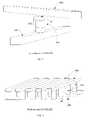
- FIG. 1is a perspective view showing an embodiment of a memory cell described in U.S. Pat. No. 6,952,030.
- FIG. 2is a perspective view of a portion of a first memory level of memory cells like those pictured in FIG. 1 .
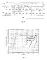
- FIG. 3is a cross-sectional view of a memory cell formed according to a preferred embodiment of the present invention.
- FIGS. 4 a - 4 dare cross-sectional views showing stages in fabrication of a first memory level comprising memory cells formed according to a preferred embodiment of the present invention.
- FIG. 5is a probability plot showing current at a read voltage of about 2 volts for various data states of a population of memory cells formed according to the present invention.
- FIG. 1shows an embodiment of a memory cell described in Herner et al., U.S. Pat. No. 6,952,030, “High-density three-dimensional memory cell,” hereinafter the '030 patent.
- pillar 300comprising a diode 302 and a dielectric rupture antifuse 18 , is disposed electrically in series between top conductor 400 and bottom conductor 200 .
- a read voltageof, for example, about 2 volts
- top conductor 400 and bottom conductor 200very little current flows between them.
- Application of a relatively large programming voltage between top conductor 400 and bottom conductor 200permanently alters the memory cell of FIG. 1 so that, after programming, significantly more current flows at the same read voltage. This difference in current under the same applied read voltage allows a programmed cell to be distinguished from an unprogrammed cell; for example for a data “0” to be distinguished from a data “1”.
- diode 302is formed of semiconductor material which, in the initial, unprogrammed device, is in a relatively high-resistivity state. Application of a programming voltage across diode 302 changes the semiconductor material from a high-resistivity state to a lower-resistivity state.
- the programming voltagemust perform two tasks. It must convert the semiconductor material of diode 302 from a high-resistivity to a low-resistivity state, and must also cause the dielectric material of dielectric rupture antifuse 18 to undergo dielectric breakdown, during which at least one conductive path is permanently formed through dielectric rupture antifuse 18 .
- FIG. 2shows a portion of a first memory level of cells like those of FIG. 1 arranged in a cross-point array comprising a plurality of memory cells.
- Each memory cellcomprises a pillar 300 (which comprises the diode 302 and antifuse 18 shown in FIG. 1 ) disposed between one of top conductors 400 and one of bottom conductors 200 .
- Top conductors 400are above bottom conductors 200 and extend in a different direction, preferably perpendicular to them. Two, three, or more such memory levels can be vertically stacked atop one another, forming a monolithic three dimensional memory array.
- a dielectric rupture antifuseis paired with a semiconductor diode formed of semiconductor material, for example silicon, where the semiconductor material of the diode is in a low-resistivity state as formed, and need not be converted.
- the diode of the '030 patent and the '549 applicationis formed by depositing a semiconductor material such as silicon in an amorphous state, then performing a thermal anneal to crystallize the silicon, forming a polycrystalline silicon or polysilicon diode.
- a semiconductor materialsuch as silicon in an amorphous state
- a thermal annealto crystallize the silicon
- the polysiliconforms with a high number of crystalline defects, causing it to be high-resistivity.
- Application of a programming pulse through this high-defect polysiliconapparently alters the polysilicon, causing it to be lower-resistivity.
- a diode formed of low-defect, low-resistivity semiconductor materialis paired with an oxide layer, where the oxide layer is preferably grown, for example thermally grown.
- the oxide layeris formed in an initial insulating or high-resistivity state.
- Application of an appropriate electrical pulseconverts the oxide layer to a low-resistivity state.
- Application of an additional electrical pulseconverts the oxide layer to a higher-resistivity state.
- the oxide layercan be reversibly switched between higher- and lower-resistivity states, forming a rewriteable memory cell.
- An electrical pulse that switches the oxide layer from a higher-resistivity state to a lower-resistivity statewill be called a set pulse.
- An electrical pulse that switches the oxide layer from a lower-resistivity state to a higher-resistivity statewill be called a reset pulse.
- the term pulse hererefers to an electrical pulse, and can be used to refer to applied voltage, to current, or both. This description will similarly refer to a set voltage or to a reset current as appropriate.
- the oxiderather than to deposit it because a grown oxide is generally denser and of higher quality than a deposited oxide.
- an oxidecan be grown in an easily integrable oxidation step, for example by thermal oxidation.
- the amplitude of the electrical pulsemay be only the amplitude required to switch the resistivity of the oxide layer.
- the semiconductor material of the diodeis already in the low-resistivity state as formed, and thus need not be converted. The amplitude of the set and reset pulses may thus be reduced and made more controllable and predictable.
- Diode 302is vertically disposed between bottom conductor 200 and top conductor 400 .
- diode 302is a vertically oriented p-i-n diode, comprising bottom heavily doped n-type region 112 , middle intrinsic or lightly doped region 114 , and top heavily doped p-type region 116 .
- the polarity of the diodecould be reversed; region 116 could be n-type while region 112 is p-type.
- Silicide layer 118is in contact with diode 302 , in this example immediately on top of it.
- This silicide layerwas preferably formed by depositing a silicide-forming metal, such as titanium, cobalt, or nickel, on the silicon and annealing to form the silicide.
- Layer 126immediately above silicide layer 118 , is a switching oxide layer. As will be described, layer 126 is preferably a grown oxide, most preferably thermally grown by exposing silicide layer 118 to an oxygen-containing ambient in elevated temperature.
- a grown oxidemay be formed by dry oxidation (i.e., exposing the silicide to an O 2 containing gas), wet oxidation (i.e., exposing the silicide to hot steam), plasma-enhanced oxidation (i.e., exposing the silicide to an oxygen plasma), chemical oxidation (i.e., exposing the silicide to an oxidizing liquid) and electrochemical oxidation (such as anodic oxidation).
- a deposited silicon oxide layerfor example, is formed on a surface by providing silicon and oxygen atoms to the surface; examples of deposition processes are chemical vapor deposition (CVD) or sputtering.
- a reset pulse between bottom conductor 200 and top conductor 400converts switching oxide layer 126 from its initial low-resistivity state to a higher-resistivity state.
- the reset pulseis preferably applied with diode 302 under reverse bias. This higher-resistivity state may correspond to a different data state of the memory cell.
- the memory cellcan be reversibly switched between data states, serving as a rewriteable cell.
- the example givendescribes two resistivity states. In other embodiments, there may be more than two reliably detectable resistivity states, which may correspond to more than two data states.
- the memory cell of FIG. 3was formed by forming a vertically oriented diode; and thermally growing an oxide layer, wherein the diode and the grown oxide layer are disposed electrically in series between a first conductor and a second conductor, wherein the memory cell comprises the diode and the grown oxide, and wherein the grown oxide layer serves as a reversible switching element.
- the vertically oriented diodeis formed by depositing the silicon, wherein at least some of the silicon is amorphous; forming a titanium or cobalt layer above the amorphous silicon; annealing to form a titanium silicide layer or a cobalt silicide layer and crystallize the amorphous silicon in contact with the silicide layer.
- a detailed examplewill be provided describing fabrication of a first memory level in a monolithic three dimensional memory array comprising memory cells formed according to the present invention. It will be understood that this example is provided for illustration only, and that the present invention may take many other forms. In this example, many details will be provided, including specific steps, materials, and conditions. As will be appreciated by those skilled in the art, however, many of these details can be altered, augmented, or omitted while the results fall within the scope of the invention.
- the '030 patentdescribed fabrication of a monolithic three dimensional memory array comprising memory cells like those of FIG. 1 . Petti et al., U.S. Pat. No.
- This substrate 100can be any semiconducting substrate as known in the art, such as monocrystalline silicon, IV-IV compounds like silicon-germanium or silicon-germanium-carbon, III-V compounds, II-VII compounds, epitaxial layers over such substrates, or any other semiconducting material.
- the semiconducting materialcan be a bulk wafer or silicon-on-insulator.
- the substratemay include integrated circuits fabricated therein.
- the insulating layer 102is formed over substrate 100 .
- the insulating layer 102can be silicon oxide, silicon nitride, high-dielectric film, Si—C—O—H film, or any other suitable insulating material.
- the first conductors 200are formed over the substrate 100 and insulator 102 .
- An optional adhesion layer 104preferably titanium nitride or some other appropriate material, is deposited first by any conventional method.
- the thickness of adhesion layer 104can range from about 20 to about 500 angstroms, preferably about 200 angstroms.
- conducting layer 106The next layer to be deposited is conducting layer 106 .
- Conducting layer 106can comprise any suitable conducting material known in the art. Conducting layer 106 must survive temperature steps that in most embodiments will exceed 650 degrees C.; thus tungsten is preferred. Tungsten layer 106 can be deposited by any CVD process or a physical vapor deposition process. In one embodiment, the thickness of conducting layer 106 can range from about 200 to about 2500 angstroms. In another embodiment, the thickness of conducting layer 106 is about 1500 angstroms.
- Layers 104 and 106are patterned and etched using any suitable masking and etching process to form substantially parallel, substantially coplanar conductors 200 , shown in FIG. 4 a in cross-section.
- the width of conductor rails 200 after etchcan range from about 300 to about 2500 angstroms. (In this discussion “width” will refer to the width of a line or feature measured in the plane substantially parallel to substrate 100 .)
- the width of the gaps between conductor rails 200preferably is substantially the same as the width of conductor rails 200 themselves, though it may be greater or less.
- Dielectric material 108is deposited over and between conductor rails 200 .
- Dielectric material 108can be any known electrically insulating material, such as silicon oxide, silicon nitride, or silicon oxynitride.
- silicon oxideis used as dielectric material 108 .
- the silicon oxidecan be deposited using any known process, such as CVD, or, for example, high density plasma CVD (HDPCVD).
- planar surface 109is shown in FIG. 4 a .
- This removal of dielectric overfill to form planar surface 109can be performed by any process known in the art, such as chemical mechanical planarization (CMP) or etchback.
- CMPchemical mechanical planarization
- etchbackthe etchback techniques described in Raghuram et al., U.S. application Ser. No. 10/883,417, “Nonselective Unpatterned Etchback to Expose Buried Patterned Features,” filed Jun. 30, 2004 and hereby incorporated by reference in its entirety, can advantageously be used.
- conductor railscan be formed by a Damascene process.
- barrier layer 110preferably of titanium nitride, is deposited as the first layer after planarization of the conductor rails. Its thickness can be, for example, about 20 to about 500 angstroms. The thickness of barrier layer 110 is preferably about 200 angstroms.
- the semiconductor materialis preferably silicon or a silicon alloy such as silicon-germanium.
- silicon-germaniuma silicon alloy such as silicon-germanium.
- the semiconductor pillaris a junction diode, comprising a bottom heavily doped region of a first conductivity type and a top heavily doped region of a second conductivity type.
- the middle regioncan intentionally be lightly doped, or it can be intrinsic, or not intentionally doped.
- An undoped regionwill never be perfectly electrically neutral, and will always have defects or contaminants that cause it to behave as if slightly n-doped or p-doped.
- Such a diodecan be considered a p-i-n diode.
- a diodewill be described having a heavily doped n-type bottom region, an intrinsic middle region, and a heavily doped p-type top region.
- junction diodeis used herein to refer to a semiconductor device with the property of conducting current more easily in one direction than the other, having two terminal electrodes, and made of semiconducting material which is p-type at one electrode and n-type at the other. Examples include p-n diodes, which have p-type semiconductor material and n-type semiconductor material in contact, and p-i-n diodes, in which intrinsic (undoped) or lightly doped semiconductor material is interposed between p-type semiconductor material and n-type semiconductor material.
- Heavily doped n-type silicon region 112is preferably doped in situ by flowing a donor gas providing atoms of an n-type dopant, preferably phosphorus, during deposition of the silicon.
- this layercan range from about 100 to about 1000 angstroms, preferably about 200 angstroms.
- the next layer 114is preferable intrinsic silicon. This layer can formed by any deposition method known in the art.
- the thickness of lightly doped n-type silicon layer 114can range from about 1000 to about 4800 angstroms, preferably about 3300 angstroms. In one embodiment, silicon is deposited without intentional doping, yet has defects which cause it to behave as though slightly n-type. Regions 112 and 114 are preferably amorphous as deposited.
- Semiconductor layers 114 and 112 just depositedwill be patterned and etched to form semiconductor pillars 300 , along with barrier layer 110 .
- Semiconductor pillars 300should have about the same pitch and about the same width as conductors 200 below, such that each semiconductor pillar 300 is formed on top of a conductor 200 . Some misalignment can be tolerated.
- the semiconductor pillars 300can be formed using any suitable masking and etching process.
- photoresistcan be deposited, patterned using standard photolithography techniques, and etched, then the photoresist removed.
- a hard mask of some other materialfor example silicon dioxide, can be formed on top of the semiconductor layer stack, with bottom antireflective coating (BARC) on top, then patterned and etched.
- BARCbottom antireflective coating
- DARCdielectric antireflective coating
- Dielectric material 108is deposited over and between the semiconductor pillars 300 , filling the gaps between them.
- the dielectric material 108 on top of the pillars 300is removed, exposing the tops of pillars 300 separated by dielectric material 108 , and leaving a substantially planar surface.
- This removal of dielectric overfillcan be performed by any process known in the art, such as CMP or etchback.
- the resulting structureis shown in FIG. 4 b .
- An ion implantation stepforms top heavily doped p-type regions 116 , completing p-i-n diodes 302 . Any appropriate p-type dopant, for example boron, may be used.
- an optional oxide, nitride, or oxynitride layer 118is formed on heavily doped regions 116 .
- a silicon dioxide layer 118is grown by oxidizing silicon at the tops of heavily doped regions 116 at about 600 to about 850 degrees C. for about 20 seconds to about two minutes, forming between about 15 and about 50 angstroms of silicon dioxide.
- Layer 118could be deposited instead. In other embodiments, layer 118 is omitted.
- silicide-forming metals to be used for this purposeinclude titanium, cobalt, chromium, tantalum, platinum, nickel, niobium, and palladium. Titanium and cobalt are preferred. This example will describe the use of titanium for layer 120 , but it will be understood that any of the other materials can be used.
- Titanium layer 120is deposited to any suitable thickness, for example between about 60 and about 200 angstroms, preferably between about 100 and about 150 angstroms, most preferably about 100 angstroms.
- titanium nitride layer 122is deposited on titanium layer 120 , preferably about 300 angstroms thick. Layers 120 and 122 can be deposited by any conventional method, for example by sputtering.
- An annealis performed between about 600 and about 800 degrees from about 10 seconds to about two minutes, preferably between about 650 degrees and about 750 degrees, most preferably at about 670 degrees for about 20 seconds, for example in nitrogen.
- the annealserves to react titanium layer 120 with heavily doped regions 116 where it overlies them to form titanium silicide. If optional oxide layer 118 was formed, it is substantially entirely reduced between titanium layer 120 and the silicon of heavily doped region 116 .
- This anneal stepwill generally also serve to crystallize the silicon of heavily doped n-type region 112 , intrinsic region 114 , heavily dope p-type region 116 . Recall that these regions were amorphous as deposited.
- titanium nitride layer 122 and unreacted titanium 120are stripped in a selective wet etch, leaving behind titanium silicide layers 124 , each formed in a disk-shaped region on the top of one of the silicon pillars 300 . Note that some thickness of top heavily doped p-type region 116 is consumed in formation of titanium silicide layer 124 .
- Conventional salicide formationincludes a second anneal following strip of the unreacted titanium to convert the titanium silicide from the high-resistivity C49 phase to the low-resistivity C54 phase. In embodiments of the present invention this step is omitted.
- Switching oxide layer 126is formed on titanium silicide layer 124 , preferably by oxidation of titanium silicide layer 124 . Oxidation is performed between about 600 and about 850 degrees for between about 20 seconds to about two minutes, preferably at about 775 degrees for about two minutes. The resulting oxide layer 126 will be primarily silicon dioxide, though some amount of titanium or titanium oxide may be included in switching oxide layer 126 . Similarly, if cobalt was used for layer 120 in place of titanium, the resulting oxide layer 126 will be primarily silicon dioxide, though some amount of cobalt or cobalt oxide may be included.
- titanium silicide layer 124 and the crystallization of silicon regions 112 , 114 , and 116are performed in a single anneal step. Titanium silicide begins to form at a temperature lower than that at which large-scale crystallization of silicon begins, however. Thus when silicide layer 124 begins to form, silicon regions 112 , 114 , and 116 are still largely amorphous, and this amorphous silicon crystallizes in contact with titanium silicide layer 124 .
- Overlying conductors 400can be formed in the same manner as underlying conductors 200 . Overlying conductors 400 will be formed at a height above the height of underlying conductors 200 , and extend in a different direction from them, preferably substantially perpendicular to them.
- the resulting structureis a bottom or first level of memory cells. Additional memory levels can be monolithically formed above the first, as described in the '030 patent and the other incorporated references, forming a monolithic three dimensional memory array. For example, a second plurality of pillars can be formed above the upper conductors, and a third plurality of conductors can be formed above them.
- the upper conductors of one memory levelcan serve as the lower conductors of an overlying memory level, or an interlevel dielectric can be formed between them.
- a monolithic three dimensional memory levelcan be formed by a) monolithically forming a first memory level above a substrate by a method comprising: i) forming a plurality of bottom conductors; ii) forming a plurality of top conductors; iii) forming a plurality of vertically oriented diodes; and iv) growing a plurality of oxide layers, wherein the first memory level comprises a first plurality of memory cells, wherein each memory cell comprises one of the diodes and one of the grown oxide layers disposed electrically in series between one of the bottom conductors and one of the top conductors, wherein, for each memory cell, the grown oxide layer serves as a reversible switching element; and b) monolithically forming a second memory level above the first.
- a monolithic three dimensional memory arrayis one in which multiple memory levels are formed above a single substrate, such as a wafer, with no intervening substrates.
- the layers forming one memory levelare deposited or grown directly over the layers of an existing level or levels.
- stacked memorieshave been constructed by forming memory levels on separate substrates and adhering the memory levels atop each other, as in Leedy, U.S. Pat. No. 5,915,167, “Three dimensional structure memory.”
- the substratesmay be thinned or removed from the memory levels before bonding, but as the memory levels are initially formed over separate substrates, such memories are not true monolithic three dimensional memory arrays.
- a monolithic three dimensional memory array formed above a substratecomprises at least a first memory level formed at a first height above the substrate and a second memory level formed at a second height different from the first height. Three, four, eight, or indeed any number of memory levels can be formed above the substrate in such a multilevel array.
- the switching oxide layer 126 of FIG. 3which in preferred embodiments is a grown oxide layer, is generally insulating as formed, such that when a read voltage is applied between bottom conductor 200 and top conductor 400 , little or no current flows between these conductors.
- switching oxide layer 126becomes lower resistivity.
- a subsequent reset pulseincreases the resistivity of switching oxide layer 126 , such that less current flows when a read voltage is applied.
- the set transitionfrom high-resistivity to low-resistivity, is voltage-based, and is achieved by applying sufficient voltage across switching oxide layer 126 .
- the reset transitionfrom low-resistivity to high-resistivity, is current-based, and is achieved when sufficient current flows across switching oxide layer 126 .
- the set transitionis preferably achieved by applying a set voltage between bottom conductor 200 and top conductor 400 of FIG. 3 such that diode 302 is forward biased.
- switching oxide layer 126undergoes the set transition, from high resistivity to low resistivity, at a voltage of about 2-3 volts across the oxide layer. (An additional voltage will be across the diode, so the voltage between bottom conductor 200 and top conductor 400 will be higher than 2-3 volts.) At this voltage, once switching oxide layer 126 has switched to the set state, in general the current isn't high enough to cause reset, and switching oxide layer 126 remains in the set state, as intended.
- Switching oxide layer 126is in the low-resistivity state. Recall that the reset transition is current-based; thus a relatively high current (in one example, about 100 to about 200 microamps) is required to cause reset to take place.
- a relatively high voltagefor example about eight volts, must be applied between conductors 200 and 400 to achieve this reset current.
- currentis the same in all elements of the circuit, including both switching oxide layer 126 and diode 302 . Voltage, however, is distributed between these elements.
- switching oxide layer 126is in the low-resistivity state. Voltage is increased between bottom conductor 200 and top conductor 400 until sufficient current flows across switching oxide layer 126 to cause it to reset; in one example this is about ⁇ 13 volts. After reset, because the diode is under reverse bias, most of the voltage is across the diode, not across switching oxide layer 126 . The relatively low voltage across switching oxide layer 126 avoids the tendency for it to spontaneously undergo an unwanted set transition after reset.
- FIG. 5is a probability plot showing read current at about 2 volts for memory cells according to the present invention. Referring FIG. 5 , this initial state of the memory cell will be referred to as the V state. In one example, under a read voltage of about 2 volts, the current between conductors 200 and 400 is about 1 nanoamp or less, or a few nanoamps.
- the memory cellAfter application of a first set pulse, preferably having voltage between about 5 and about 8 volts, the memory cell is converted to a second state, which will be referred to as the P state.
- the set voltageis preferably positive; i.e. the diode is under forward bias.
- Switching oxide layer 126undergoes a set transition; i.e. it is converted from the initial high-resistivity state to a lower-resistivity state, indicated in FIG. 5 by the arrow labeled “V to P”.
- V to PAt an applied read voltage of about 2 volts, current between conductors 200 and 400 when the memory cell is in the P state is on the order of tens of microamps.
- the memory cellAfter application of a first reset pulse, preferably having voltage of about ⁇ 13 volts, the memory cell is converted to a third state, which will be referred to as the R state.
- the reset voltageis preferably negative; i.e. the diode is under reverse bias.
- Switching oxide layer 126undergoes a reset transition; i.e. it is converted from a lower-resistivity state to a higher-resistivity state, transition “P to R” in FIG. 5 .
- current between conductors 200 and 400 when the memory cell is in the R stateis hundreds of nanoamps.
- the memory cellAfter application of a second set pulse, preferably having voltage of about 5 to about 8 volts, the memory cell is converted to a fourth state, which will be referred to as the S state.
- the set voltageagain is preferably positive, with the diode under forward bias.
- Switching oxide layer 126is converted from a higher-resistivity state to a lower-resistivity state; this transition is “R to S” in FIG. 5 .
- current between conductors 200 and 400 when the memory cell is in the S stateis a few microamps.
- the initial cell state Vwas the lowest-current state
- the second cell state Pwas the highest-current state. It was found, in one embodiment, that it can be difficult to return to either of these states.
- Reset transitionsput the cell in the R state, a lower-current state with current of hundreds of nanoamps, but did not return it to the initial V state, with current of a few nanoamps.
- the first set transitionput the cell into the P state, having current of tens of microamps
- subsequent set transitionsput the cell in the S state, having current of only a few microamps, but did not return it to the higher current of the P state. It proved possible to repeatably and reliably switch between the R and S states, however.
- such a cellcould serve as a rewriteable cell which is repeatably switched between the R and the S states, each of which corresponds to a data state.
- the “R to S” and “S to R” transitions of FIG. 5are repeated each time the cell is written or erased.
- such a cellcould serve as a one-time-programmable cell having four data states corresponding to the V, P, R, and S states.
- the current ranges of the S state and the P statewere undesirably close.
- the memory cellcould be treated as a one-time programmable cell having three states, the V state, the P state, and the R state.
- a rewriteable memory cell formed according to embodiments of the present inventionmay have three or more data states.
- a one-time programmable cell formed according to embodiments of the present inventionmay have five or more data states.
- diode 302 adjacent to silicide layer 124causes diode 302 to be formed of polysilicon which is low-defect and low-resistivity as formed, and that this polysilicon does not change in resistivity. It is believed that the change in current between the V, P, R, and S states of the memory cell is due to changes in the resistivity of switching oxide 126 .
Landscapes
- Engineering & Computer Science (AREA)
- Chemical & Material Sciences (AREA)
- Materials Engineering (AREA)
- Computer Hardware Design (AREA)
- Semiconductor Memories (AREA)
Abstract
Description
- This application is related to Schricker et al., U.S. patent application Ser. No. ______, “Memory Cell That Employs a Selectively Grown Reversible Resistance-Switching Element and Methods of Forming the Same,” (atty. docket no. SD-MD-335×); to Schricker et al., U.S. patent application Ser. No. ______, “Memory Cell That Employs a Selectively Grown Reversible Resistance-Switching Element and Methods of Forming the Same,” (atty. docket no. SD-MD-335Y); to Schricker et al., U.S. patent application Ser. No. ______, “Memory Cell That Employs a Selectively Deposited Reversible Resistance-Switching Element and Methods of Forming the Same,” (atty. docket no. SD-MD-333×); and to Schricker et al., U.S. patent application Ser. No. ______, “Memory Cell That Employs a Selectively Deposited Reversible Resistance-Switching Element and Methods of Forming the Same,” (atty. docket no. SD-MD-333Y), all owned by the assignee of the present invention and all hereby incorporated by reference, and all filed on even date herewith.
- A diode can be paired with a dielectric rupture antifuse to form a one-time-programmable nonvolatile memory cell having two data states. Similarly, a diode can be paired with a reversible resistivity-switching element to form a rewriteable nonvolatile memory cell. Use of known resistivity-switching materials, such as chalcogenides, can present fabrication challenges, however.
- It would be advantageous to form a memory cell comprising a diode formed in series with a resistivity-switching element, wherein fabrication of the resistivity-switching element is easily integrated into the process of forming the memory cell.
- The present invention is defined by the following claims, and nothing in this section should be taken as a limitation on those claims. In general, the invention is directed to a rewriteable memory cell formed by pairing a switching oxide layer with a diode. Preferably the switching oxide layer is a grown oxide.
- A first aspect of the invention provides for a method for forming a rewriteable memory cell, the method comprising: forming a vertically oriented diode; and thermally growing an oxide layer, wherein the diode and the grown oxide layer are disposed electrically in series between a first conductor and a second conductor, wherein the memory cell comprises the diode and the grown oxide, and wherein the grown oxide layer serves as a reversible switching element.
- A preferred embodiment of the invention provides for a method for forming a monolithic three dimensional memory array, the method comprising: a) monolithically forming a first memory level above a substrate by a method comprising: i) forming a plurality of bottom conductors; ii) forming a plurality of top conductors; iii) forming a plurality of vertically oriented diodes; and iv) growing a plurality of oxide layers, wherein the first memory level comprises a first plurality of memory cells, wherein each memory cell comprises one of the diodes and one of the grown oxide layers disposed electrically in series between one of the bottom conductors and one of the top conductors, wherein, for each memory cell, the grown oxide layer serves as a reversible switching element; and b) monolithically forming a second memory level above the first.
- Each of the aspects and embodiments of the invention described herein can be used alone or in combination with one another.
- The preferred aspects and embodiments will now be described with reference to the attached drawings.
FIG. 1 is a perspective view showing an embodiment of a memory cell described in U.S. Pat. No. 6,952,030.FIG. 2 is a perspective view of a portion of a first memory level of memory cells like those pictured inFIG. 1 .FIG. 3 is a cross-sectional view of a memory cell formed according to a preferred embodiment of the present invention.FIGS. 4 a-4dare cross-sectional views showing stages in fabrication of a first memory level comprising memory cells formed according to a preferred embodiment of the present invention.FIG. 5 is a probability plot showing current at a read voltage of about 2 volts for various data states of a population of memory cells formed according to the present invention.FIG. 1 shows an embodiment of a memory cell described in Herner et al., U.S. Pat. No. 6,952,030, “High-density three-dimensional memory cell,” hereinafter the '030 patent. In this nonvolatile memory cell,pillar 300, comprising adiode 302 and adielectric rupture antifuse 18, is disposed electrically in series betweentop conductor 400 andbottom conductor 200. In the initial state of this memory cell, when a read voltage of, for example, about 2 volts, is applied betweentop conductor 400 andbottom conductor 200, very little current flows between them. Application of a relatively large programming voltage betweentop conductor 400 andbottom conductor 200 permanently alters the memory cell ofFIG. 1 so that, after programming, significantly more current flows at the same read voltage. This difference in current under the same applied read voltage allows a programmed cell to be distinguished from an unprogrammed cell; for example for a data “0” to be distinguished from a data “1”.- As described in detail in Herner et al., U.S. patent application Ser. No. 10/955,549, “Nonvolatile Memory Cell Without a Dielectric Antifuse Having High- and Low-Impedance States,” filed Sep. 29, 2004 and hereinafter the '549 application; and in Herner et al., U.S. patent application Ser. No. 11/148,530, “Nonvolatile Memory Cell Operating by Increasing Order in Polycrystalline Semiconductor Material,” filed Jun. 8, 2005, and hereinafter the '530 application, both owned by the assignee of the present invention and hereby incorporated by reference,
diode 302 is formed of semiconductor material which, in the initial, unprogrammed device, is in a relatively high-resistivity state. Application of a programming voltage acrossdiode 302 changes the semiconductor material from a high-resistivity state to a lower-resistivity state. - In a cell like that shown in
FIG. 1 , the programming voltage must perform two tasks. It must convert the semiconductor material ofdiode 302 from a high-resistivity to a low-resistivity state, and must also cause the dielectric material ofdielectric rupture antifuse 18 to undergo dielectric breakdown, during which at least one conductive path is permanently formed throughdielectric rupture antifuse 18. FIG. 2 shows a portion of a first memory level of cells like those ofFIG. 1 arranged in a cross-point array comprising a plurality of memory cells. Each memory cell comprises a pillar300 (which comprises thediode 302 andantifuse 18 shown inFIG. 1 ) disposed between one oftop conductors 400 and one ofbottom conductors 200.Top conductors 400 are abovebottom conductors 200 and extend in a different direction, preferably perpendicular to them. Two, three, or more such memory levels can be vertically stacked atop one another, forming a monolithic three dimensional memory array.- In Herner, U.S. Pat. No. 7,176,064, “Memory Cell Comprising a Semiconductor Junction Diode Crystallized Adjacent to a Silicide,” hereinafter the '064 patent and hereby incorporated by reference, a dielectric rupture antifuse is paired with a semiconductor diode formed of semiconductor material, for example silicon, where the semiconductor material of the diode is in a low-resistivity state as formed, and need not be converted.
- The diode of the '030 patent and the '549 application is formed by depositing a semiconductor material such as silicon in an amorphous state, then performing a thermal anneal to crystallize the silicon, forming a polycrystalline silicon or polysilicon diode. As described in the '530 application, when deposited amorphous silicon is crystallized in contact solely with materials with which it has a high lattice mismatch, such as silicon dioxide and titanium nitride, the polysilicon forms with a high number of crystalline defects, causing it to be high-resistivity. Application of a programming pulse through this high-defect polysilicon apparently alters the polysilicon, causing it to be lower-resistivity.
- It has been found, however, that when deposited amorphous silicon is crystallized in contact with a layer of an appropriate silicide, for example titanium silicide or cobalt silicide, the resulting crystallized silicon is much higher quality, with fewer defects, and has lower resistivity. The lattice spacing of titanium silicide or cobalt silicide is very close to that of silicon, and it is believed that when amorphous silicon is crystallized in contact with a layer of an appropriate silicide at a favorable orientation, the silicide provides a template for crystal growth of silicon, minimizing defects. Unlike the high-defect silicon crystallized adjacent only to materials with which it has a high lattice mismatch, application of a large electrical pulse does not appreciably change the resistivity of this low-defect, low-resistivity silicon crystallized in contact with the silicide layer.
- In the present invention a diode formed of low-defect, low-resistivity semiconductor material is paired with an oxide layer, where the oxide layer is preferably grown, for example thermally grown. The oxide layer is formed in an initial insulating or high-resistivity state. Application of an appropriate electrical pulse converts the oxide layer to a low-resistivity state. Application of an additional electrical pulse converts the oxide layer to a higher-resistivity state. The oxide layer can be reversibly switched between higher- and lower-resistivity states, forming a rewriteable memory cell.
- An electrical pulse that switches the oxide layer from a higher-resistivity state to a lower-resistivity state will be called a set pulse. An electrical pulse that switches the oxide layer from a lower-resistivity state to a higher-resistivity state will be called a reset pulse. The term pulse here refers to an electrical pulse, and can be used to refer to applied voltage, to current, or both. This description will similarly refer to a set voltage or to a reset current as appropriate.
- It is preferred to grow the oxide rather than to deposit it because a grown oxide is generally denser and of higher quality than a deposited oxide. Further, an oxide can be grown in an easily integrable oxidation step, for example by thermal oxidation. By pairing this switchable oxide layer with a diode formed of low-defect, low-resistivity semiconductor material, the amplitude of the electrical pulse may be only the amplitude required to switch the resistivity of the oxide layer. The semiconductor material of the diode is already in the low-resistivity state as formed, and thus need not be converted. The amplitude of the set and reset pulses may thus be reduced and made more controllable and predictable.
- A preferred embodiment of the present invention is the memory cell shown in cross-section in
FIG. 3 .Diode 302 is vertically disposed betweenbottom conductor 200 andtop conductor 400. In thisexample diode 302 is a vertically oriented p-i-n diode, comprising bottom heavily doped n-type region 112, middle intrinsic or lightly dopedregion 114, and top heavily doped p-type region 116. Clearly the polarity of the diode could be reversed;region 116 could be n-type whileregion 112 is p-type. Silicide layer 118 is in contact withdiode 302, in this example immediately on top of it. This silicide layer was preferably formed by depositing a silicide-forming metal, such as titanium, cobalt, or nickel, on the silicon and annealing to form the silicide.Layer 126, immediately abovesilicide layer 118, is a switching oxide layer. As will be described,layer 126 is preferably a grown oxide, most preferably thermally grown by exposingsilicide layer 118 to an oxygen-containing ambient in elevated temperature. For example, a grown oxide may be formed by dry oxidation (i.e., exposing the silicide to an O2containing gas), wet oxidation (i.e., exposing the silicide to hot steam), plasma-enhanced oxidation (i.e., exposing the silicide to an oxygen plasma), chemical oxidation (i.e., exposing the silicide to an oxidizing liquid) and electrochemical oxidation (such as anodic oxidation). In contrast to a grown oxide layer, a deposited silicon oxide layer, for example, is formed on a surface by providing silicon and oxygen atoms to the surface; examples of deposition processes are chemical vapor deposition (CVD) or sputtering.- When the memory cell is formed, when a read voltage is applied between
bottom conductor 200 andtop conductor 400, very little current flows between them. Application of a set pulse betweenbottom conductor 200 andtop conductor 400, acrossdiode 302,silicide layer 118, and switchingoxide layer 126, changes the resistivity of switchingoxide layer 126. The set pulse is preferably applied withdiode 302 under forward bias. After application of the set pulse, when the same read voltage is applied betweenbottom conductor 200 andtop conductor 400, substantially more current flows between them. This higher-current state will be referred to as the set state, and may correspond to a data state of the cell. - Application of a reset pulse between
bottom conductor 200 andtop conductor 400 converts switchingoxide layer 126 from its initial low-resistivity state to a higher-resistivity state. The reset pulse is preferably applied withdiode 302 under reverse bias. This higher-resistivity state may correspond to a different data state of the memory cell. By applying additional set pulses and reset pulses, the memory cell can be reversibly switched between data states, serving as a rewriteable cell. - For simplicity, the example given describes two resistivity states. In other embodiments, there may be more than two reliably detectable resistivity states, which may correspond to more than two data states.
- To summarize, the memory cell of
FIG. 3 was formed by forming a vertically oriented diode; and thermally growing an oxide layer, wherein the diode and the grown oxide layer are disposed electrically in series between a first conductor and a second conductor, wherein the memory cell comprises the diode and the grown oxide, and wherein the grown oxide layer serves as a reversible switching element. In preferred embodiments the vertically oriented diode is formed by depositing the silicon, wherein at least some of the silicon is amorphous; forming a titanium or cobalt layer above the amorphous silicon; annealing to form a titanium silicide layer or a cobalt silicide layer and crystallize the amorphous silicon in contact with the silicide layer. - A detailed example will be provided describing fabrication of a first memory level in a monolithic three dimensional memory array comprising memory cells formed according to the present invention. It will be understood that this example is provided for illustration only, and that the present invention may take many other forms. In this example, many details will be provided, including specific steps, materials, and conditions. As will be appreciated by those skilled in the art, however, many of these details can be altered, augmented, or omitted while the results fall within the scope of the invention. The '030 patent described fabrication of a monolithic three dimensional memory array comprising memory cells like those of
FIG. 1 . Petti et al., U.S. Pat. No. 6,946,719, “Semiconductor Device Including Junction Diode Contacting Contact-Antifuse Unit Comprising Silicide,” hereby incorporated by reference, describes fabrication of a monolithic three dimensional memory array comprising a related memory cell. For clarity, not all of the details of these patents and earlier incorporated patent and applications will be included, but it will be understood that no teaching of these applications is intended to be excluded. - Fabrication of a single memory level is described in detail. Additional memory levels can be stacked, each monolithically formed above the one below it.
- Turning to
FIG. 4 a, formation of the memory begins with asubstrate 100. Thissubstrate 100 can be any semiconducting substrate as known in the art, such as monocrystalline silicon, IV-IV compounds like silicon-germanium or silicon-germanium-carbon, III-V compounds, II-VII compounds, epitaxial layers over such substrates, or any other semiconducting material. The semiconducting material can be a bulk wafer or silicon-on-insulator. The substrate may include integrated circuits fabricated therein. - An insulating
layer 102 is formed oversubstrate 100. The insulatinglayer 102 can be silicon oxide, silicon nitride, high-dielectric film, Si—C—O—H film, or any other suitable insulating material. - The
first conductors 200 are formed over thesubstrate 100 andinsulator 102. Anoptional adhesion layer 104, preferably titanium nitride or some other appropriate material, is deposited first by any conventional method. The thickness ofadhesion layer 104 can range from about 20 to about 500 angstroms, preferably about 200 angstroms. - The next layer to be deposited is conducting
layer 106. Conductinglayer 106 can comprise any suitable conducting material known in the art. Conductinglayer 106 must survive temperature steps that in most embodiments will exceed 650 degrees C.; thus tungsten is preferred.Tungsten layer 106 can be deposited by any CVD process or a physical vapor deposition process. In one embodiment, the thickness of conductinglayer 106 can range from about 200 to about 2500 angstroms. In another embodiment, the thickness of conductinglayer 106 is about 1500 angstroms. Layers coplanar conductors 200, shown inFIG. 4 ain cross-section. The width ofconductor rails 200 after etch can range from about 300 to about 2500 angstroms. (In this discussion “width” will refer to the width of a line or feature measured in the plane substantially parallel tosubstrate 100.) The width of the gaps betweenconductor rails 200 preferably is substantially the same as the width ofconductor rails 200 themselves, though it may be greater or less.- Next a
dielectric material 108 is deposited over and between conductor rails200.Dielectric material 108 can be any known electrically insulating material, such as silicon oxide, silicon nitride, or silicon oxynitride. In a preferred embodiment, silicon oxide is used asdielectric material 108. The silicon oxide can be deposited using any known process, such as CVD, or, for example, high density plasma CVD (HDPCVD). - Finally, excess
dielectric material 108 on top ofconductor rails 200 is removed, exposing the tops ofconductor rails 200 separated bydielectric material 108, and leaving a substantiallyplanar surface 109. The resulting structure is shown inFIG. 4 a. This removal of dielectric overfill to formplanar surface 109 can be performed by any process known in the art, such as chemical mechanical planarization (CMP) or etchback. For example, the etchback techniques described in Raghuram et al., U.S. application Ser. No. 10/883,417, “Nonselective Unpatterned Etchback to Expose Buried Patterned Features,” filed Jun. 30, 2004 and hereby incorporated by reference in its entirety, can advantageously be used. Alternatively, conductor rails can be formed by a Damascene process. - Next, turning to
FIG. 4 b, vertical semiconductor pillars will be formed above completed conductor rails200. (To savespace substrate 100 is omitted inFIG. 4 band subsequent figures.) In preferred embodiments,barrier layer 110, preferably of titanium nitride, is deposited as the first layer after planarization of the conductor rails. Its thickness can be, for example, about 20 to about 500 angstroms. The thickness ofbarrier layer 110 is preferably about 200 angstroms. - Next semiconductor material that will be patterned into pillars is deposited. The semiconductor material is preferably silicon or a silicon alloy such as silicon-germanium. For simplicity, this description will refer to the semiconductor material as silicon, but it will be understood that other materials may be substituted.
- In preferred embodiments, the semiconductor pillar is a junction diode, comprising a bottom heavily doped region of a first conductivity type and a top heavily doped region of a second conductivity type. The middle region can intentionally be lightly doped, or it can be intrinsic, or not intentionally doped. An undoped region will never be perfectly electrically neutral, and will always have defects or contaminants that cause it to behave as if slightly n-doped or p-doped. Such a diode can be considered a p-i-n diode. In the present example, a diode will be described having a heavily doped n-type bottom region, an intrinsic middle region, and a heavily doped p-type top region.
- The term junction diode is used herein to refer to a semiconductor device with the property of conducting current more easily in one direction than the other, having two terminal electrodes, and made of semiconducting material which is p-type at one electrode and n-type at the other. Examples include p-n diodes, which have p-type semiconductor material and n-type semiconductor material in contact, and p-i-n diodes, in which intrinsic (undoped) or lightly doped semiconductor material is interposed between p-type semiconductor material and n-type semiconductor material.
- Heavily doped n-
type silicon region 112 is preferably doped in situ by flowing a donor gas providing atoms of an n-type dopant, preferably phosphorus, during deposition of the silicon. In a preferred embodiment, this layer can range from about 100 to about 1000 angstroms, preferably about 200 angstroms. - The
next layer 114 is preferable intrinsic silicon. This layer can formed by any deposition method known in the art. The thickness of lightly doped n-type silicon layer 114 can range from about 1000 to about 4800 angstroms, preferably about 3300 angstroms. In one embodiment, silicon is deposited without intentional doping, yet has defects which cause it to behave as though slightly n-type.Regions - Semiconductor layers114 and112 just deposited will be patterned and etched to form
semiconductor pillars 300, along withbarrier layer 110.Semiconductor pillars 300 should have about the same pitch and about the same width asconductors 200 below, such that eachsemiconductor pillar 300 is formed on top of aconductor 200. Some misalignment can be tolerated. - The
semiconductor pillars 300 can be formed using any suitable masking and etching process. For example, photoresist can be deposited, patterned using standard photolithography techniques, and etched, then the photoresist removed. Alternatively, a hard mask of some other material, for example silicon dioxide, can be formed on top of the semiconductor layer stack, with bottom antireflective coating (BARC) on top, then patterned and etched. Similarly, dielectric antireflective coating (DARC) can be used as a hard mask. - The photolithography techniques described in Chen, U.S. Pat. No. 7,172,840, “Photomask Features with Interior Nonprinting Window Using Alternating Phase Shifting”; or Chen, U.S. application Ser. No. 10/815,312, Photomask Features with Chromeless Nonprinting Phase Shifting Window,” filed Apr. 1, 2004, both owned by the assignee of the present invention and hereby incorporated by reference, can advantageously be used to perform any photolithography step used in formation of a memory array according to the present invention.
Dielectric material 108 is deposited over and between thesemiconductor pillars 300, filling the gaps between them. Next thedielectric material 108 on top of thepillars 300 is removed, exposing the tops ofpillars 300 separated bydielectric material 108, and leaving a substantially planar surface. This removal of dielectric overfill can be performed by any process known in the art, such as CMP or etchback. The resulting structure is shown inFIG. 4 b. An ion implantation step forms top heavily doped p-type regions 116, completingp-i-n diodes 302. Any appropriate p-type dopant, for example boron, may be used.- Turning to
FIG. 4 c, an optional oxide, nitride, oroxynitride layer 118 is formed on heavily dopedregions 116. In some embodiments, as shown, asilicon dioxide layer 118 is grown by oxidizing silicon at the tops of heavily dopedregions 116 at about 600 to about 850 degrees C. for about 20 seconds to about two minutes, forming between about 15 and about 50 angstroms of silicon dioxide.Layer 118 could be deposited instead. In other embodiments,layer 118 is omitted. - Next a
layer 120 of a silicide-forming metal is deposited. Preferred silicide-forming metals to be used for this purpose include titanium, cobalt, chromium, tantalum, platinum, nickel, niobium, and palladium. Titanium and cobalt are preferred. This example will describe the use of titanium forlayer 120, but it will be understood that any of the other materials can be used. Titanium layer 120 is deposited to any suitable thickness, for example between about 60 and about 200 angstroms, preferably between about 100 and about 150 angstroms, most preferably about 100 angstroms. To prevent oxidation oftitanium layer 120,titanium nitride layer 122 is deposited ontitanium layer 120, preferably about 300 angstroms thick.Layers - An anneal is performed between about 600 and about 800 degrees from about 10 seconds to about two minutes, preferably between about 650 degrees and about 750 degrees, most preferably at about 670 degrees for about 20 seconds, for example in nitrogen. The anneal serves to react
titanium layer 120 with heavily dopedregions 116 where it overlies them to form titanium silicide. Ifoptional oxide layer 118 was formed, it is substantially entirely reduced betweentitanium layer 120 and the silicon of heavily dopedregion 116. This anneal step will generally also serve to crystallize the silicon of heavily doped n-type region 112,intrinsic region 114, heavily dope p-type region 116. Recall that these regions were amorphous as deposited. - Turning to
FIG. 4 d, as in a conventional salicide process,titanium nitride layer 122 andunreacted titanium 120 are stripped in a selective wet etch, leaving behindtitanium silicide layers 124, each formed in a disk-shaped region on the top of one of thesilicon pillars 300. Note that some thickness of top heavily doped p-type region 116 is consumed in formation oftitanium silicide layer 124. - Conventional salicide formation includes a second anneal following strip of the unreacted titanium to convert the titanium silicide from the high-resistivity C49 phase to the low-resistivity C54 phase. In embodiments of the present invention this step is omitted.
Switching oxide layer 126 is formed ontitanium silicide layer 124, preferably by oxidation oftitanium silicide layer 124. Oxidation is performed between about 600 and about 850 degrees for between about 20 seconds to about two minutes, preferably at about 775 degrees for about two minutes. The resultingoxide layer 126 will be primarily silicon dioxide, though some amount of titanium or titanium oxide may be included in switchingoxide layer 126. Similarly, if cobalt was used forlayer 120 in place of titanium, the resultingoxide layer 126 will be primarily silicon dioxide, though some amount of cobalt or cobalt oxide may be included.- Note that in this example the silicide reaction forming
titanium silicide layer 124 and the crystallization ofsilicon regions silicide layer 124 begins to form,silicon regions titanium silicide layer 124. - Overlying
conductors 400 can be formed in the same manner asunderlying conductors 200. Overlyingconductors 400 will be formed at a height above the height ofunderlying conductors 200, and extend in a different direction from them, preferably substantially perpendicular to them. The resulting structure is a bottom or first level of memory cells. Additional memory levels can be monolithically formed above the first, as described in the '030 patent and the other incorporated references, forming a monolithic three dimensional memory array. For example, a second plurality of pillars can be formed above the upper conductors, and a third plurality of conductors can be formed above them. The upper conductors of one memory level can serve as the lower conductors of an overlying memory level, or an interlevel dielectric can be formed between them. - To summarize, a monolithic three dimensional memory level can be formed by a) monolithically forming a first memory level above a substrate by a method comprising: i) forming a plurality of bottom conductors; ii) forming a plurality of top conductors; iii) forming a plurality of vertically oriented diodes; and iv) growing a plurality of oxide layers, wherein the first memory level comprises a first plurality of memory cells, wherein each memory cell comprises one of the diodes and one of the grown oxide layers disposed electrically in series between one of the bottom conductors and one of the top conductors, wherein, for each memory cell, the grown oxide layer serves as a reversible switching element; and b) monolithically forming a second memory level above the first.
- A monolithic three dimensional memory array is one in which multiple memory levels are formed above a single substrate, such as a wafer, with no intervening substrates. The layers forming one memory level are deposited or grown directly over the layers of an existing level or levels. In contrast, stacked memories have been constructed by forming memory levels on separate substrates and adhering the memory levels atop each other, as in Leedy, U.S. Pat. No. 5,915,167, “Three dimensional structure memory.” The substrates may be thinned or removed from the memory levels before bonding, but as the memory levels are initially formed over separate substrates, such memories are not true monolithic three dimensional memory arrays.
- A monolithic three dimensional memory array formed above a substrate comprises at least a first memory level formed at a first height above the substrate and a second memory level formed at a second height different from the first height. Three, four, eight, or indeed any number of memory levels can be formed above the substrate in such a multilevel array.
- As described earlier, the switching
oxide layer 126 ofFIG. 3 , which in preferred embodiments is a grown oxide layer, is generally insulating as formed, such that when a read voltage is applied betweenbottom conductor 200 andtop conductor 400, little or no current flows between these conductors. When a set pulse is applied, switchingoxide layer 126 becomes lower resistivity. When the same read voltage is applied betweenbottom conductor 200 andtop conductor 400, substantially more current flows. A subsequent reset pulse increases the resistivity of switchingoxide layer 126, such that less current flows when a read voltage is applied. - In general, it is believed that the set transition, from high-resistivity to low-resistivity, is voltage-based, and is achieved by applying sufficient voltage across switching
oxide layer 126. In contrast, it is believed that the reset transition, from low-resistivity to high-resistivity, is current-based, and is achieved when sufficient current flows across switchingoxide layer 126. - The set transition is preferably achieved by applying a set voltage between
bottom conductor 200 andtop conductor 400 ofFIG. 3 such thatdiode 302 is forward biased. In general, switchingoxide layer 126 undergoes the set transition, from high resistivity to low resistivity, at a voltage of about 2-3 volts across the oxide layer. (An additional voltage will be across the diode, so the voltage betweenbottom conductor 200 andtop conductor 400 will be higher than 2-3 volts.) At this voltage, once switchingoxide layer 126 has switched to the set state, in general the current isn't high enough to cause reset, and switchingoxide layer 126 remains in the set state, as intended. - A problem may arise when an attempt is made to reset switching
oxide layer 126 with the diode under forward bias.Switching oxide layer 126 is in the low-resistivity state. Recall that the reset transition is current-based; thus a relatively high current (in one example, about 100 to about 200 microamps) is required to cause reset to take place. In forward bias, a relatively high voltage, for example about eight volts, must be applied betweenconductors oxide layer 126 anddiode 302. Voltage, however, is distributed between these elements. After switching (after the reset transition is achieved, and switchingoxide layer 126 has become high-resistivity), most of the voltage is across switchingoxide 126 rather than across the diode. This relatively high voltage may be sufficient to immediately cause switchingoxide 126 to undergo an unwanted set conversion, back to the low-resistivity state from which it was just switched. Thus with the diode in forward bias, it may be difficult to causeswitching oxide 126 to remain in the reset state. - Instead, suppose the reset transition is performed with the diode under reverse bias. Again, switching
oxide layer 126 is in the low-resistivity state. Voltage is increased betweenbottom conductor 200 andtop conductor 400 until sufficient current flows across switchingoxide layer 126 to cause it to reset; in one example this is about −13 volts. After reset, because the diode is under reverse bias, most of the voltage is across the diode, not across switchingoxide layer 126. The relatively low voltage across switchingoxide layer 126 avoids the tendency for it to spontaneously undergo an unwanted set transition after reset. - Thus it is preferred to perform the set transition with diode forward-biased and the reset transition with the diode reverse-biased. As described in Kumar et al., U.S. patent application Ser. No. 11/496,986, “Method For Using A Memory Cell Comprising Switchable Semiconductor Memory Element With Trimmable Resistance,” filed Jul. 31, 2006, and hereby incorporated by reference, performing the reset transition with the diode in reverse bias has the additional advantage of reducing leakage current across unselected memory cells in the array.
- When the memory cell is initially formed, switching
oxide layer 126 is in its initial high-resistivity state.FIG. 5 , is a probability plot showing read current at about 2 volts for memory cells according to the present invention. ReferringFIG. 5 , this initial state of the memory cell will be referred to as the V state. In one example, under a read voltage of about 2 volts, the current betweenconductors - After application of a first set pulse, preferably having voltage between about 5 and about 8 volts, the memory cell is converted to a second state, which will be referred to as the P state. The set voltage is preferably positive; i.e. the diode is under forward bias.
Switching oxide layer 126 undergoes a set transition; i.e. it is converted from the initial high-resistivity state to a lower-resistivity state, indicated inFIG. 5 by the arrow labeled “V to P”. At an applied read voltage of about 2 volts, current betweenconductors Switching oxide layer 126 undergoes a reset transition; i.e. it is converted from a lower-resistivity state to a higher-resistivity state, transition “P to R” inFIG. 5 . At an applied read voltage of about 2 volts, current betweenconductors - After application of a second set pulse, preferably having voltage of about 5 to about 8 volts, the memory cell is converted to a fourth state, which will be referred to as the S state. The set voltage again is preferably positive, with the diode under forward bias.
Switching oxide layer 126 is converted from a higher-resistivity state to a lower-resistivity state; this transition is “R to S” inFIG. 5 . At an applied read voltage of about 2 volts, current betweenconductors - In this example, the initial cell state V was the lowest-current state, while the second cell state P was the highest-current state. It was found, in one embodiment, that it can be difficult to return to either of these states. Reset transitions put the cell in the R state, a lower-current state with current of hundreds of nanoamps, but did not return it to the initial V state, with current of a few nanoamps. Similarly, the first set transition put the cell into the P state, having current of tens of microamps, while subsequent set transitions put the cell in the S state, having current of only a few microamps, but did not return it to the higher current of the P state. It proved possible to repeatably and reliably switch between the R and S states, however.
- Thus in one embodiment, such a cell could serve as a rewriteable cell which is repeatably switched between the R and the S states, each of which corresponds to a data state. In this embodiment, the “R to S” and “S to R” transitions of
FIG. 5 are repeated each time the cell is written or erased. In such a cell, it may be desirable not to use the V and the P states as data states, and to apply the first set and reset pulses before the memory cell reaches the end user. - In an alternative embodiment, such a cell could serve as a one-time-programmable cell having four data states corresponding to the V, P, R, and S states. In some instances, the current ranges of the S state and the P state were undesirably close. In this case, the memory cell could be treated as a one-time programmable cell having three states, the V state, the P state, and the R state.
- In alternative embodiments, a rewriteable memory cell formed according to embodiments of the present invention may have three or more data states. Similarly, a one-time programmable cell formed according to embodiments of the present invention may have five or more data states.
- As described, it is believed that crystallizing the silicon of
diode 302 adjacent tosilicide layer 124 causesdiode 302 to be formed of polysilicon which is low-defect and low-resistivity as formed, and that this polysilicon does not change in resistivity. It is believed that the change in current between the V, P, R, and S states of the memory cell is due to changes in the resistivity of switchingoxide 126. - It may be, however, that some degree of resistivity switching takes place in the polysilicon that makes up
diode 302 as well as in switchingoxide layer 126, as described in Kumar et al., earlier incorporated. - Detailed methods of fabrication have been described herein, but any other methods that form the same structures can be used while the results fall within the scope of the invention.
- The foregoing detailed description has described only a few of the many forms that this invention can take. For this reason, this detailed description is intended by way of illustration, and not by way of limitation. It is only the following claims, including all equivalents, which are intended to define the scope of this invention.
Claims (22)
Priority Applications (3)
| Application Number | Priority Date | Filing Date | Title |
|---|---|---|---|
| US11/772,081US20090104756A1 (en) | 2007-06-29 | 2007-06-29 | Method to form a rewriteable memory cell comprising a diode and a resistivity-switching grown oxide |
| PCT/US2008/007992WO2009005706A2 (en) | 2007-06-29 | 2008-06-27 | Method to form a rewriteable memory cell comprising a diode and a resistivity-switching grown oxide |
| TW097124467ATW200915540A (en) | 2007-06-29 | 2008-06-27 | Method to form a rewriteable memory cell comprising a diode and a resistivity-switching grown oxide |
Applications Claiming Priority (1)
| Application Number | Priority Date | Filing Date | Title |
|---|---|---|---|
| US11/772,081US20090104756A1 (en) | 2007-06-29 | 2007-06-29 | Method to form a rewriteable memory cell comprising a diode and a resistivity-switching grown oxide |
Publications (1)
| Publication Number | Publication Date |
|---|---|
| US20090104756A1true US20090104756A1 (en) | 2009-04-23 |
Family
ID=40226719
Family Applications (1)
| Application Number | Title | Priority Date | Filing Date |
|---|---|---|---|
| US11/772,081AbandonedUS20090104756A1 (en) | 2007-06-29 | 2007-06-29 | Method to form a rewriteable memory cell comprising a diode and a resistivity-switching grown oxide |
Country Status (3)
| Country | Link |
|---|---|
| US (1) | US20090104756A1 (en) |
| TW (1) | TW200915540A (en) |
| WO (1) | WO2009005706A2 (en) |
Cited By (14)
| Publication number | Priority date | Publication date | Assignee | Title |
|---|---|---|---|---|
| US20060250837A1 (en)* | 2005-05-09 | 2006-11-09 | Sandisk 3D, Llc | Nonvolatile memory cell comprising a diode and a resistance-switching material |
| US20070114509A1 (en)* | 2005-11-23 | 2007-05-24 | Sandisk 3D Llc | Memory cell comprising nickel-cobalt oxide switching element |
| US20070228414A1 (en)* | 2006-03-31 | 2007-10-04 | Sandisk 3D, Llc | Heterojunction device comprising a semiconductor and a resistivity-switching oxide or nitride |
| US20070236981A1 (en)* | 2006-03-31 | 2007-10-11 | Sandisk 3D, Llc | Multilevel nonvolatile memory cell comprising a resistivity-switching oxide or nitride and an antifuse |
| US20090001342A1 (en)* | 2007-06-29 | 2009-01-01 | April Schricker | Memory cell that employs a selectively grown reversible resistance-switching element and methods of forming the same |
| US20090001343A1 (en)* | 2007-06-29 | 2009-01-01 | April Schricker | Memory cell that employs a selectively deposited reversible resistance-switching element and methods of forming the same |
| US20090001344A1 (en)* | 2007-06-29 | 2009-01-01 | April Schricker | Memory cell that employs a selectively grown reversible resistance-switching element and methods of forming the same |
| US20090001345A1 (en)* | 2007-06-29 | 2009-01-01 | April Schricker | Memory cell that employs a selectively deposited reversible resistance-switching element and methods of forming the same |
| US7816659B2 (en) | 2005-11-23 | 2010-10-19 | Sandisk 3D Llc | Devices having reversible resistivity-switching metal oxide or nitride layer with added metal |
| US7829875B2 (en) | 2006-03-31 | 2010-11-09 | Sandisk 3D Llc | Nonvolatile rewritable memory cell comprising a resistivity-switching oxide or nitride and an antifuse |
| WO2018051062A3 (en)* | 2016-09-14 | 2018-04-26 | Arm Ltd | A cem switching device |
| US10121967B2 (en) | 2016-11-29 | 2018-11-06 | Arm Limited | CEM switching device |
| US10128438B2 (en) | 2016-09-09 | 2018-11-13 | Arm Limited | CEM switching device |
| US11636316B2 (en) | 2018-01-31 | 2023-04-25 | Cerfe Labs, Inc. | Correlated electron switch elements for brain-based computing |
Citations (38)
| Publication number | Priority date | Publication date | Assignee | Title |
|---|---|---|---|---|
| US3717852A (en)* | 1971-09-17 | 1973-02-20 | Ibm | Electronically rewritable read-only memory using via connections |
| US3795977A (en)* | 1971-12-30 | 1974-03-12 | Ibm | Methods for fabricating bistable resistors |
| US4203123A (en)* | 1977-12-12 | 1980-05-13 | Burroughs Corporation | Thin film memory device employing amorphous semiconductor materials |
| US4772571A (en)* | 1984-09-14 | 1988-09-20 | Stc Plc | Process of self aligned nitridation of TiSi2 to form TiN/TiSi2 contact |
| US4907054A (en)* | 1987-11-10 | 1990-03-06 | Thomson-Csf | Matrix of photosensitive elements combining a phototransistor with a storage capacitor |
| US5075738A (en)* | 1988-03-28 | 1991-12-24 | Canon Kabushiki Kaisha | Switching device and method of preparing it |
| US5087509A (en)* | 1989-05-22 | 1992-02-11 | Mitsubishi Metal Corporation | Substrate used for fabrication of thick film circuit |
| US5854102A (en)* | 1996-03-01 | 1998-12-29 | Micron Technology, Inc. | Vertical diode structures with low series resistance |
| US5915167A (en)* | 1997-04-04 | 1999-06-22 | Elm Technology Corporation | Three dimensional structure memory |
| US20020168852A1 (en)* | 2001-05-11 | 2002-11-14 | Harshfield Steven T. | PCRAM memory cell and method of making same |
| US20030031045A1 (en)* | 2001-08-08 | 2003-02-13 | Keiji Hosotani | Magnetic random access memory including memory cell unit and reference cell unit |
| US6534841B1 (en)* | 2001-12-14 | 2003-03-18 | Hewlett-Packard Company | Continuous antifuse material in memory structure |
| US20030052330A1 (en)* | 2001-09-20 | 2003-03-20 | Klein Rita J. | Electro-and electroless plating of metal in the manufacture of PCRAM devices |
| US20030193053A1 (en)* | 2002-04-10 | 2003-10-16 | Gilton Terry L. | Thin film diode integrated with chalcogenide memory cell |
| US6754097B2 (en)* | 2002-09-03 | 2004-06-22 | Hewlett-Packard Development Company, L.P. | Read operations on multi-bit memory cells in resistive cross point arrays |
| US6778425B1 (en)* | 1999-09-27 | 2004-08-17 | Matsushita Electric Industrial Co., Ltd. | Magnetoresistance effect memory device and method for producing the same |
| US20040159835A1 (en)* | 2001-08-13 | 2004-08-19 | Krieger Juri Heinrich | Memory device |
| US20040262591A1 (en)* | 2003-06-03 | 2004-12-30 | Campbell Kristy A. | Diode/superionic conductor/polymer memory structure |
| US20050052915A1 (en)* | 2002-12-19 | 2005-03-10 | Matrix Semiconductor, Inc. | Nonvolatile memory cell without a dielectric antifuse having high- and low-impedance states |
| US20050121743A1 (en)* | 2003-12-03 | 2005-06-09 | Matrix Semiconductor, Inc. | Memory cell comprising a semiconductor junction diode crystallized adjacent to a silicide |
| US20050167699A1 (en)* | 2003-10-23 | 2005-08-04 | Matsushita Electric Industrial Co., Ltd. | Variable resistance element, method of manufacturing the element, memory containing the element, and method of driving the memory |
| US20050221200A1 (en)* | 2004-04-01 | 2005-10-06 | Matrix Semiconductor, Inc. | Photomask features with chromeless nonprinting phase shifting window |
| US20050226067A1 (en)* | 2002-12-19 | 2005-10-13 | Matrix Semiconductor, Inc. | Nonvolatile memory cell operating by increasing order in polycrystalline semiconductor material |
| US7053445B1 (en)* | 2005-08-02 | 2006-05-30 | Spansion Llc | Memory device with barrier layer |
| US20060131554A1 (en)* | 2004-12-21 | 2006-06-22 | Young-Soo Joung | Nonvolatile memory device having two or more resistance elements and methods of forming and using the same |
| US20060181920A1 (en)* | 2005-02-09 | 2006-08-17 | Klaus-Dieter Ufert | Resistive memory element with shortened erase time |
| US7172840B2 (en)* | 2003-12-05 | 2007-02-06 | Sandisk Corporation | Photomask features with interior nonprinting window using alternating phase shifting |
| US20070072360A1 (en)* | 2005-09-28 | 2007-03-29 | Tanmay Kumar | Method for using a memory cell comprising switchable semiconductor memory element with trimmable resistance |
| US20070228414A1 (en)* | 2006-03-31 | 2007-10-04 | Sandisk 3D, Llc | Heterojunction device comprising a semiconductor and a resistivity-switching oxide or nitride |
| US7307013B2 (en)* | 2004-06-30 | 2007-12-11 | Sandisk 3D Llc | Nonselective unpatterned etchback to expose buried patterned features |
| US20080175032A1 (en)* | 2007-01-23 | 2008-07-24 | Kabushiki Kaisha Toshiba | Semiconductor memory and method for manufacturing the same |
| US7405465B2 (en)* | 2004-09-29 | 2008-07-29 | Sandisk 3D Llc | Deposited semiconductor structure to minimize n-type dopant diffusion and method of making |
| US20090001342A1 (en)* | 2007-06-29 | 2009-01-01 | April Schricker | Memory cell that employs a selectively grown reversible resistance-switching element and methods of forming the same |
| US7501331B2 (en)* | 2006-03-31 | 2009-03-10 | Sandisk 3D Llc | Low-temperature metal-induced crystallization of silicon-germanium films |
| US20090200640A1 (en)* | 2006-04-28 | 2009-08-13 | Yasunari Hosoi | Variable resistive element, and its manufacturing method |
| US20090236581A1 (en)* | 2006-11-30 | 2009-09-24 | Fujitsu Limited | Resistance memory element, method of manufacturing resistance memory element and semiconductor memory device |
| US20100302836A1 (en)* | 2005-05-09 | 2010-12-02 | Herner S Brad | Nonvolatile memory cell comprising a diode and a resistance-switching material |
| US7989789B2 (en)* | 2002-04-04 | 2011-08-02 | Kabushiki Kaisha Toshiba | Phase-change memory device that stores information in a non-volatile manner by changing states of a memory material |
Family Cites Families (2)
| Publication number | Priority date | Publication date | Assignee | Title |
|---|---|---|---|---|
| WO2004061851A2 (en)* | 2002-12-19 | 2004-07-22 | Matrix Semiconductor, Inc | An improved method for making high-density nonvolatile memory |
| US6946719B2 (en)* | 2003-12-03 | 2005-09-20 | Matrix Semiconductor, Inc | Semiconductor device including junction diode contacting contact-antifuse unit comprising silicide |
- 2007
- 2007-06-29USUS11/772,081patent/US20090104756A1/ennot_activeAbandoned
- 2008
- 2008-06-27WOPCT/US2008/007992patent/WO2009005706A2/enactiveApplication Filing
- 2008-06-27TWTW097124467Apatent/TW200915540A/enunknown
Patent Citations (39)
| Publication number | Priority date | Publication date | Assignee | Title |
|---|---|---|---|---|
| US3717852A (en)* | 1971-09-17 | 1973-02-20 | Ibm | Electronically rewritable read-only memory using via connections |
| US3795977A (en)* | 1971-12-30 | 1974-03-12 | Ibm | Methods for fabricating bistable resistors |
| US4203123A (en)* | 1977-12-12 | 1980-05-13 | Burroughs Corporation | Thin film memory device employing amorphous semiconductor materials |
| US4772571A (en)* | 1984-09-14 | 1988-09-20 | Stc Plc | Process of self aligned nitridation of TiSi2 to form TiN/TiSi2 contact |
| US4907054A (en)* | 1987-11-10 | 1990-03-06 | Thomson-Csf | Matrix of photosensitive elements combining a phototransistor with a storage capacitor |
| US5075738A (en)* | 1988-03-28 | 1991-12-24 | Canon Kabushiki Kaisha | Switching device and method of preparing it |
| US5087509A (en)* | 1989-05-22 | 1992-02-11 | Mitsubishi Metal Corporation | Substrate used for fabrication of thick film circuit |
| US5854102A (en)* | 1996-03-01 | 1998-12-29 | Micron Technology, Inc. | Vertical diode structures with low series resistance |
| US5915167A (en)* | 1997-04-04 | 1999-06-22 | Elm Technology Corporation | Three dimensional structure memory |
| US6778425B1 (en)* | 1999-09-27 | 2004-08-17 | Matsushita Electric Industrial Co., Ltd. | Magnetoresistance effect memory device and method for producing the same |
| US20020168852A1 (en)* | 2001-05-11 | 2002-11-14 | Harshfield Steven T. | PCRAM memory cell and method of making same |
| US20030031045A1 (en)* | 2001-08-08 | 2003-02-13 | Keiji Hosotani | Magnetic random access memory including memory cell unit and reference cell unit |
| US20040159835A1 (en)* | 2001-08-13 | 2004-08-19 | Krieger Juri Heinrich | Memory device |
| US20030052330A1 (en)* | 2001-09-20 | 2003-03-20 | Klein Rita J. | Electro-and electroless plating of metal in the manufacture of PCRAM devices |
| US6534841B1 (en)* | 2001-12-14 | 2003-03-18 | Hewlett-Packard Company | Continuous antifuse material in memory structure |
| US7989789B2 (en)* | 2002-04-04 | 2011-08-02 | Kabushiki Kaisha Toshiba | Phase-change memory device that stores information in a non-volatile manner by changing states of a memory material |
| US20030193053A1 (en)* | 2002-04-10 | 2003-10-16 | Gilton Terry L. | Thin film diode integrated with chalcogenide memory cell |
| US6754097B2 (en)* | 2002-09-03 | 2004-06-22 | Hewlett-Packard Development Company, L.P. | Read operations on multi-bit memory cells in resistive cross point arrays |
| US20050052915A1 (en)* | 2002-12-19 | 2005-03-10 | Matrix Semiconductor, Inc. | Nonvolatile memory cell without a dielectric antifuse having high- and low-impedance states |
| US20050226067A1 (en)* | 2002-12-19 | 2005-10-13 | Matrix Semiconductor, Inc. | Nonvolatile memory cell operating by increasing order in polycrystalline semiconductor material |
| US20040262591A1 (en)* | 2003-06-03 | 2004-12-30 | Campbell Kristy A. | Diode/superionic conductor/polymer memory structure |
| US20050167699A1 (en)* | 2003-10-23 | 2005-08-04 | Matsushita Electric Industrial Co., Ltd. | Variable resistance element, method of manufacturing the element, memory containing the element, and method of driving the memory |
| US20050121743A1 (en)* | 2003-12-03 | 2005-06-09 | Matrix Semiconductor, Inc. | Memory cell comprising a semiconductor junction diode crystallized adjacent to a silicide |
| US7172840B2 (en)* | 2003-12-05 | 2007-02-06 | Sandisk Corporation | Photomask features with interior nonprinting window using alternating phase shifting |
| US20050221200A1 (en)* | 2004-04-01 | 2005-10-06 | Matrix Semiconductor, Inc. | Photomask features with chromeless nonprinting phase shifting window |
| US7307013B2 (en)* | 2004-06-30 | 2007-12-11 | Sandisk 3D Llc | Nonselective unpatterned etchback to expose buried patterned features |
| US20090026582A1 (en)* | 2004-09-29 | 2009-01-29 | Sandisk 3D Llc | Deposited semiconductor structure to minimize n-type dopant diffusion and method of making |
| US7405465B2 (en)* | 2004-09-29 | 2008-07-29 | Sandisk 3D Llc | Deposited semiconductor structure to minimize n-type dopant diffusion and method of making |
| US20060131554A1 (en)* | 2004-12-21 | 2006-06-22 | Young-Soo Joung | Nonvolatile memory device having two or more resistance elements and methods of forming and using the same |
| US20060181920A1 (en)* | 2005-02-09 | 2006-08-17 | Klaus-Dieter Ufert | Resistive memory element with shortened erase time |
| US20100302836A1 (en)* | 2005-05-09 | 2010-12-02 | Herner S Brad | Nonvolatile memory cell comprising a diode and a resistance-switching material |
| US7053445B1 (en)* | 2005-08-02 | 2006-05-30 | Spansion Llc | Memory device with barrier layer |
| US20070072360A1 (en)* | 2005-09-28 | 2007-03-29 | Tanmay Kumar | Method for using a memory cell comprising switchable semiconductor memory element with trimmable resistance |
| US20070228414A1 (en)* | 2006-03-31 | 2007-10-04 | Sandisk 3D, Llc | Heterojunction device comprising a semiconductor and a resistivity-switching oxide or nitride |
| US7501331B2 (en)* | 2006-03-31 | 2009-03-10 | Sandisk 3D Llc | Low-temperature metal-induced crystallization of silicon-germanium films |
| US20090200640A1 (en)* | 2006-04-28 | 2009-08-13 | Yasunari Hosoi | Variable resistive element, and its manufacturing method |
| US20090236581A1 (en)* | 2006-11-30 | 2009-09-24 | Fujitsu Limited | Resistance memory element, method of manufacturing resistance memory element and semiconductor memory device |
| US20080175032A1 (en)* | 2007-01-23 | 2008-07-24 | Kabushiki Kaisha Toshiba | Semiconductor memory and method for manufacturing the same |
| US20090001342A1 (en)* | 2007-06-29 | 2009-01-01 | April Schricker | Memory cell that employs a selectively grown reversible resistance-switching element and methods of forming the same |
Cited By (34)
| Publication number | Priority date | Publication date | Assignee | Title |
|---|---|---|---|---|
| US7812404B2 (en) | 2005-05-09 | 2010-10-12 | Sandisk 3D Llc | Nonvolatile memory cell comprising a diode and a resistance-switching material |
| US8687410B2 (en) | 2005-05-09 | 2014-04-01 | Sandisk 3D Llc | Nonvolatile memory cell comprising a diode and a resistance-switching material |
| US20060250837A1 (en)* | 2005-05-09 | 2006-11-09 | Sandisk 3D, Llc | Nonvolatile memory cell comprising a diode and a resistance-switching material |
| US20070114509A1 (en)* | 2005-11-23 | 2007-05-24 | Sandisk 3D Llc | Memory cell comprising nickel-cobalt oxide switching element |
| US7834338B2 (en) | 2005-11-23 | 2010-11-16 | Sandisk 3D Llc | Memory cell comprising nickel-cobalt oxide switching element |
| US7816659B2 (en) | 2005-11-23 | 2010-10-19 | Sandisk 3D Llc | Devices having reversible resistivity-switching metal oxide or nitride layer with added metal |
| US8592792B2 (en) | 2006-03-31 | 2013-11-26 | Sandisk 3D Llc | Heterojunction device comprising a semiconductor oxide and a resistivity-switching oxide or nitride |
| US7875871B2 (en) | 2006-03-31 | 2011-01-25 | Sandisk 3D Llc | Heterojunction device comprising a semiconductor and a resistivity-switching oxide or nitride |
| US7808810B2 (en) | 2006-03-31 | 2010-10-05 | Sandisk 3D Llc | Multilevel nonvolatile memory cell comprising a resistivity-switching oxide or nitride and an antifuse |
| US20070228414A1 (en)* | 2006-03-31 | 2007-10-04 | Sandisk 3D, Llc | Heterojunction device comprising a semiconductor and a resistivity-switching oxide or nitride |
| US20070236981A1 (en)* | 2006-03-31 | 2007-10-11 | Sandisk 3D, Llc | Multilevel nonvolatile memory cell comprising a resistivity-switching oxide or nitride and an antifuse |
| US8227787B2 (en) | 2006-03-31 | 2012-07-24 | Sandisk 3D Llc | Heterojunction device comprising a semiconductor and a resistivity-switching oxide or nitride |
| US7829875B2 (en) | 2006-03-31 | 2010-11-09 | Sandisk 3D Llc | Nonvolatile rewritable memory cell comprising a resistivity-switching oxide or nitride and an antifuse |
| US20110114913A1 (en)* | 2006-03-31 | 2011-05-19 | Tanmay Kumar | Heterojunction device comprising a semiconductor and a resistivity-switching oxide or nitride |
| US20090001342A1 (en)* | 2007-06-29 | 2009-01-01 | April Schricker | Memory cell that employs a selectively grown reversible resistance-switching element and methods of forming the same |
| US8507315B2 (en) | 2007-06-29 | 2013-08-13 | Sandisk 3D Llc | Memory cell that employs a selectively grown reversible resistance-switching element and methods of forming the same |
| US7902537B2 (en) | 2007-06-29 | 2011-03-08 | Sandisk 3D Llc | Memory cell that employs a selectively grown reversible resistance-switching element and methods of forming the same |
| US20090001345A1 (en)* | 2007-06-29 | 2009-01-01 | April Schricker | Memory cell that employs a selectively deposited reversible resistance-switching element and methods of forming the same |
| US20110147693A1 (en)* | 2007-06-29 | 2011-06-23 | April Schricker | Memory cell that employs a selectively grown reversible resistance-switching element and methods of forming the same |
| US8173486B2 (en) | 2007-06-29 | 2012-05-08 | Sandisk 3D Llc | Memory cell that employs a selectively grown reversible resistance-switching element and methods of forming the same |
| US7824956B2 (en) | 2007-06-29 | 2010-11-02 | Sandisk 3D Llc | Memory cell that employs a selectively grown reversible resistance-switching element and methods of forming the same |
| US8233308B2 (en) | 2007-06-29 | 2012-07-31 | Sandisk 3D Llc | Memory cell that employs a selectively deposited reversible resistance-switching element and methods of forming the same |
| US8373150B2 (en) | 2007-06-29 | 2013-02-12 | Sandisk 3D, Llc | Memory cell that employs a selectively grown reversible resistance-switching element and methods of forming the same |
| US7846785B2 (en) | 2007-06-29 | 2010-12-07 | Sandisk 3D Llc | Memory cell that employs a selectively deposited reversible resistance-switching element and methods of forming the same |
| US20090001343A1 (en)* | 2007-06-29 | 2009-01-01 | April Schricker | Memory cell that employs a selectively deposited reversible resistance-switching element and methods of forming the same |
| US20090001344A1 (en)* | 2007-06-29 | 2009-01-01 | April Schricker | Memory cell that employs a selectively grown reversible resistance-switching element and methods of forming the same |
| US8809114B2 (en) | 2007-06-29 | 2014-08-19 | Sandisk 3D Llc | Memory cell that employs a selectively grown reversible resistance-switching element and methods of forming the same |
| US8816315B2 (en) | 2007-06-29 | 2014-08-26 | Sandisk 3D Llc | Memory cell that employs a selectively grown reversible resistance-switching element and methods of forming the same |
| US8913417B2 (en) | 2007-06-29 | 2014-12-16 | Sandisk 3D Llc | Memory cell that employs a selectively deposited reversible resistance-switching element and methods of forming the same |
| US10128438B2 (en) | 2016-09-09 | 2018-11-13 | Arm Limited | CEM switching device |
| WO2018051062A3 (en)* | 2016-09-14 | 2018-04-26 | Arm Ltd | A cem switching device |
| US10103327B2 (en) | 2016-09-14 | 2018-10-16 | Arm Limited | CEM switching device |
| US10121967B2 (en) | 2016-11-29 | 2018-11-06 | Arm Limited | CEM switching device |
| US11636316B2 (en) | 2018-01-31 | 2023-04-25 | Cerfe Labs, Inc. | Correlated electron switch elements for brain-based computing |
Also Published As
| Publication number | Publication date |
|---|---|
| WO2009005706A2 (en) | 2009-01-08 |
| WO2009005706A3 (en) | 2009-03-19 |
| TW200915540A (en) | 2009-04-01 |
Similar Documents
| Publication | Publication Date | Title |
|---|---|---|
| US20090104756A1 (en) | Method to form a rewriteable memory cell comprising a diode and a resistivity-switching grown oxide | |
| US7982209B2 (en) | Memory cell comprising a carbon nanotube fabric element and a steering element | |
| US7667999B2 (en) | Method to program a memory cell comprising a carbon nanotube fabric and a steering element | |
| US9025372B2 (en) | Large array of upward pointing p-i-n diodes having large and uniform current | |
| US7767499B2 (en) | Method to form upward pointing p-i-n diodes having large and uniform current | |
| US8687410B2 (en) | Nonvolatile memory cell comprising a diode and a resistance-switching material | |
| US7875871B2 (en) | Heterojunction device comprising a semiconductor and a resistivity-switching oxide or nitride | |
| US20060250836A1 (en) | Rewriteable memory cell comprising a diode and a resistance-switching material | |
| US20090086521A1 (en) | Multiple antifuse memory cells and methods to form, program, and sense the same | |
| US20060273298A1 (en) | Rewriteable memory cell comprising a transistor and resistance-switching material in series | |
| US20060157683A1 (en) | Nonvolatile phase change memory cell having a reduced thermal contact area | |
| WO2008118486A1 (en) | Memory cell comprising a carbon nanotube fabric element and a steering element and methods of forming the same |
Legal Events
| Date | Code | Title | Description |
|---|---|---|---|
| AS | Assignment | Owner name:SANDISK 3D, LLC, CALIFORNIA Free format text:ASSIGNMENT OF ASSIGNORS INTEREST;ASSIGNOR:KUMAR, TANMAY;REEL/FRAME:019845/0541 Effective date:20070724 | |
| STCB | Information on status: application discontinuation | Free format text:ABANDONED -- FAILURE TO RESPOND TO AN OFFICE ACTION | |
| AS | Assignment | Owner name:SANDISK TECHNOLOGIES INC., TEXAS Free format text:ASSIGNMENT OF ASSIGNORS INTEREST;ASSIGNOR:SANDISK 3D LLC.;REEL/FRAME:038300/0665 Effective date:20160324 | |
| AS | Assignment | Owner name:SANDISK TECHNOLOGIES INC., TEXAS Free format text:CORRECTIVE ASSIGNMENT TO CORRECT THE INCORRECT LISTED PATENT NUMBER 8853569 TO THE CORRECT PATENT NUMBER 8883569 PREVIOUSLY RECORDED ON REEL 038300 FRAME 0665. ASSIGNOR(S) HEREBY CONFIRMS THE ASSIGNMENT;ASSIGNOR:SANDISK 3D LLC;REEL/FRAME:038520/0552 Effective date:20160324 | |
| AS | Assignment | Owner name:SANDISK TECHNOLOGIES LLC, TEXAS Free format text:CHANGE OF NAME;ASSIGNOR:SANDISK TECHNOLOGIES INC;REEL/FRAME:038807/0980 Effective date:20160516 |