US20090103378A1 - Single-strobe operation of memory devices - Google Patents
Single-strobe operation of memory devicesDownload PDFInfo
- Publication number
- US20090103378A1 US20090103378A1US11/873,475US87347507AUS2009103378A1US 20090103378 A1US20090103378 A1US 20090103378A1US 87347507 AUS87347507 AUS 87347507AUS 2009103378 A1US2009103378 A1US 2009103378A1
- Authority
- US
- United States
- Prior art keywords
- strobe
- signal
- packet
- strobe signal
- memory device
- Prior art date
- Legal status (The legal status is an assumption and is not a legal conclusion. Google has not performed a legal analysis and makes no representation as to the accuracy of the status listed.)
- Granted
Links
Images


Classifications
- G—PHYSICS
- G11—INFORMATION STORAGE
- G11C—STATIC STORES
- G11C7/00—Arrangements for writing information into, or reading information out from, a digital store
- G—PHYSICS
- G06—COMPUTING OR CALCULATING; COUNTING
- G06F—ELECTRIC DIGITAL DATA PROCESSING
- G06F13/00—Interconnection of, or transfer of information or other signals between, memories, input/output devices or central processing units
- G06F13/14—Handling requests for interconnection or transfer
- G06F13/16—Handling requests for interconnection or transfer for access to memory bus
- G06F13/1668—Details of memory controller
- G06F13/1689—Synchronisation and timing concerns
- G—PHYSICS
- G11—INFORMATION STORAGE
- G11C—STATIC STORES
- G11C7/00—Arrangements for writing information into, or reading information out from, a digital store
- G11C7/10—Input/output [I/O] data interface arrangements, e.g. I/O data control circuits, I/O data buffers
- G11C7/1051—Data output circuits, e.g. read-out amplifiers, data output buffers, data output registers, data output level conversion circuits
- G11C7/1066—Output synchronization
- G—PHYSICS
- G11—INFORMATION STORAGE
- G11C—STATIC STORES
- G11C7/00—Arrangements for writing information into, or reading information out from, a digital store
- G11C7/10—Input/output [I/O] data interface arrangements, e.g. I/O data control circuits, I/O data buffers
- G11C7/1072—Input/output [I/O] data interface arrangements, e.g. I/O data control circuits, I/O data buffers for memories with random access ports synchronised on clock signal pulse trains, e.g. synchronous memories, self timed memories
- G—PHYSICS
- G11—INFORMATION STORAGE
- G11C—STATIC STORES
- G11C7/00—Arrangements for writing information into, or reading information out from, a digital store
- G11C7/10—Input/output [I/O] data interface arrangements, e.g. I/O data control circuits, I/O data buffers
- G11C7/1078—Data input circuits, e.g. write amplifiers, data input buffers, data input registers, data input level conversion circuits
- G11C7/109—Control signal input circuits
- G—PHYSICS
- G11—INFORMATION STORAGE
- G11C—STATIC STORES
- G11C7/00—Arrangements for writing information into, or reading information out from, a digital store
- G11C7/10—Input/output [I/O] data interface arrangements, e.g. I/O data control circuits, I/O data buffers
- G11C7/1078—Data input circuits, e.g. write amplifiers, data input buffers, data input registers, data input level conversion circuits
- G11C7/1093—Input synchronization
Definitions
- the present applicationrelates generally to a controller and at least one controlled memory device and, more specifically, to methods and apparatus adapting the controller and the memory device to a single-strobe mode of operation.
- Double-data-rate synchronous dynamic random access memory(DDR SDRAM) is an example of such an arrangement.
- DDR SDRAMDouble-data-rate synchronous dynamic random access memory
- the controllerplaces data on a data bus while indicating, on a command bus, a write command, and indicating, on an address bus, a location on the particular memory device at which the data is to be stored.
- the controllerindicates, on the command bus, a read command, and indicates, on an address bus, a location on the particular memory device from which the data is to be read.
- the memory deviceresponds to the read command and address by placing the requested read data on the data bus.
- memory devicesare arranged in a ring or loop.
- the data connectionmay, for example, be a multibit bus.
- a data signal received at the first memory device on the data connectionis passed on to a second memory device on an other data connection and a data signal received at the second memory device on the other data connection is passed on to a third memory device on a further data connection, etc.
- the data signalpropagates around the ring until the data signal is returned to the controller.
- there are additional signals also propagating through the ringinclude a Command Strobe signal; and a Data Strobe signal.
- the controllerFor a write operation, the controller causes the Command Strobe signal to transition from “0” to “1” to indicate the start of a Command and Write Data Packet. Simultaneously, the controller starts to transmit, on the data connection, a Command and Write Data Packet that includes: a write command indicating a particular memory device and address to which data is to be written followed by the data that is to be written. The controller then causes the Command Strobe signal to transition from “1” to “0” to indicate the end of the Command and Write Data Packet.
- the controllerFor a read operation, the controller causes the Data Strobe signal to transition from “0” to “1” to indicate the start of a Read Data Packet. Simultaneously, the controller starts to transmit, on the data connection, a read data packet that includes: a read command indicating a particular memory device and address from which the data is to be read. The controller then causes the Command Strobe signal to transition from “1” to “0” to indicate the end of the Read Data Packet. Subsequently, the controller causes the Data Strobe signal to transition from “0” to “1” to indicate, to the particular memory device, that the requested read data is be transmitted on the data connection.
- a read commandprimes a memory device for a read data transfer.
- the length of a readis arbitrary and interruptible since the end of the read data transfer operation is determined by a transition of the Data Strobe signal from “1” to “0”.
- the length of a writeis arbitrary and interruptible since the end of the write data transfer operation is determined by a transition of the Command Strobe signal from “1” to “0”.
- packetsoriginate at a controller and flow unidirectionally through a ring of memory devices and back to the controller.
- Different configurationsare possible based on either distributing a clock in parallel or sourcing the clock synchronously along with the data and strobes.
- the second configurationhas more pin overhead than the first configuration based on extra differential clock output pins.
- Pin overheadcontinues to be a carefully monitored quality of interfaces between devices, such as the interface between the controller and the first memory device or between memory devices, with a lower pin overhead being desirable. That is, it is desirable to reduce the ratio of control pins to data pins.
- FIG. 1illustrates a ring arrangement of memory devices configured for parallel clock distribution
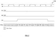
- FIG. 2illustrates a timing diagram for Command and Write Data Packet timing for the arrangement of FIG. 1 ;
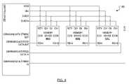
- FIG. 3illustrates a timing diagram for a Read Data Packet timing for the arrangement of FIG. 1 ;
- FIG. 4illustrates an arrangement of memory devices configured for parallel clock distribution according to example embodiments
- FIG. 5illustrates a memory device for use in the arrangement of FIG. 4 according to example embodiments
- FIG. 6illustrates a packet header decoder for use in the memory device of FIG. 5 according to example embodiments
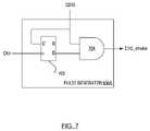
- FIG. 7illustrates a first pulse generator for use in the packet header decoder of FIG. 6 according to example embodiments
- FIG. 8illustrates a second pulse generator for use in the packet header decoder of FIG. 6 according to example embodiments
- FIG. 9illustrates a strobe generator for use in the packet header decoder of FIG. 6 according to example embodiments
- FIG. 10illustrates a timing diagram for the first pulse generator of FIG. 7 ;
- FIG. 11illustrates a timing diagram for the strobe generator of FIG. 9 ;
- FIG. 12illustrates a timing diagram for the handling of a Command and Write Data Packet by the memory device of FIG. 5 ;
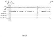
- FIG. 13illustrates a timing diagram for the handling of a Read Data Packet by the memory device of FIG. 5 .
- the total number of signal inputs (e.g., pins) on a semiconductor memory devicemay be reduced through the use of a unique interface design. Operation with only one strobe signal pin may be accomplished, without reducing functionality, through the transmission of a primary packet that includes a “packet header” and a payload, where the packet header contains encoded information about the type of the payload.
- the payloadmay, for instance, be a secondary packet, e.g., the original packet that would have been transmitted in a system using more than one strobe.
- a method of controlling a memory deviceincludes transmitting a strobe signal delimiting a primary packet and concurrently transmitting said primary packet on a data bus, the primary packet including a packet header followed by a payload, the packet header indicating a type to be associated with the payload.
- a memory device controlleris provided for carrying out this method and a computer readable medium is provided for adapting a memory device controller to carry out this method.
- a memory deviceincludes an internal memory device and a packet header decoder.
- the internal memory deviceincludes a plurality of data bus inputs for receiving a signal on a data bus, a first strobe input for receiving a first strobe signal indicating that the signal on the data bus relates to a first type of packet and a second strobe input for receiving a second strobe signal indicating that the signal on the data bus relates to a second type of packet.
- the packet header decoderincludes a clock input for receiving a system clock signal, an inverse clock input for receiving an inverse system clock signal, a data bus input for receiving a portion of the signal on the data bus, a third strobe input for receiving a third strobe signal, a pulse generator for generating a fourth strobe signal based on the inverse system clock signal and the third strobe signal and a strobe generator for generating one of the first strobe signal and the second strobe signal based on: the system clock signal; the portion of the signal on the data bus; and the fourth strobe signal.
- a memory arrangementincluding a memory controller and a memory device.
- the memory controllerincludes a strobe output for transmitting a third strobe signal delimiting a primary packet and a plurality of data bus outputs for transmitting the primary packet on a data bus, the primary packet including a packet header followed by a payload, the packet header indicating a type to be associated with the payload.
- the memory deviceincludes an internal memory device and a packet header decoder.
- the internal memory deviceincludes a plurality of data bus inputs for receiving the primary packet on the data bus, a first strobe input for receiving a first strobe signal indicating that the signal on the data bus relates to a first type of packet and a second strobe input for receiving a second strobe signal indicating that the signal on the data bus relates to a second type of packet.
- the packet header decoderincludes a clock input for receiving a system clock signal, an inverse clock input for receiving an inverse system clock signal, a data bus input for receiving a portion of the primary packet on the data bus, a third strobe input for receiving the third strobe signal, a pulse generator for generating a fourth strobe signal based on the inverse system clock signal and the third strobe signal and a strobe generator for generating one of the first strobe signal and the second strobe signal based on: the system clock signal; the portion of the primary packet on the data bus; and the fourth strobe signal.
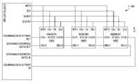
- a first memory device 104 A, a second memory device 104 B and a third memory device 104 Care in a ring or loop arrangement. Operation of the memory devices 104 for writing or reading is organized by a controller 102 .
- the controller 102may, as is typical, include a processor (not shown) and the processor may be provided with computer readable instructions for executing methods exemplary of the present application from a software medium (not shown) which could be a disk, a tape, a chip, a flash memory card or a random access memory containing a file downloaded from a remote source.
- the controller 102is connected to the first memory device 104 A by way of a Command Strobe Line, a Data Strobe Line and a data bus.
- the first memory device 104 Ais connected to the second memory device 104 B by way of a Command Strobe Line, a Data Strobe Line and a data bus.
- the second memory device 104 Bis connected to the third memory device 104 C by way of a Command Strobe Line, a Data Strobe Line and a data bus.
- the third memory device 104 Cis connected to the controller 102 by way of a Command Strobe Line, a Data Strobe Line and a data bus.
- the controller 102is also connected to each of the memory devices 104 , in parallel, by a Reset line, a Chip Enable line, a Clock line and an inverse Clock line.
- Inputs to the memory device 104 on the (possibly multibit) data busmay be representative of a command, representative of data, representative of a target device address, or representative of an address within the memory device.
- Inputs on the data busmay be captured (shifted in to registers) on the crossing of the signal on the System Clock line (CK) with the signal on the Inverted System Clock line (CK#) when the signal on the Chip Enable (CE#) line is at a logical LOW and the signal on the Command Strobe line (received at the CSI pin) is at a logical HIGH.
- Output on the data busmay be synchronously shifted out at the crossing of the signal on the System Clock line (CK) with the signal on the Inverted System Clock line (CK#) when the signal on the Chip Enable (CE#) line is at a logical LOW and the signal on the Data Strobe line (received at the Data Strobe In, “DSI”, pin) is at a logical HIGH.
- CKSystem Clock line
- CK#Inverted System Clock line
- DSIData Strobe In
- a first memory device 404 A, a second memory device 404 B and a third memory device 404 Care in a ring or loop arrangement. Operation of the memory devices 404 for writing or reading is organized by a controller 402 .
- the controller 402is connected to the first memory device 404 A by way of a unidirectional, point-to-point data bus and a Command/Data Strobe line.
- the first memory device 404 Ais connected to the second memory device 404 B by way of a unidirectional, point-to-point data bus and a Command/Data Strobe line.
- the second memory device 404 Bis connected to the third memory device 404 C by way of a unidirectional, point-to-point data bus and a Command/Data Strobe line.
- the third memory device 404 Cis connected to the controller 402 by way of a unidirectional, point-to-point data bus and a Command/Data Strobe line.
- the controller 402is also connected to each of the memory devices 404 , in parallel, by a Reset line, a Chip Enable line, a Clock line and an inverse Clock line.
- FIG. 5illustrates an example structure for the first memory device 404 A and, correspondingly, the other memory devices 404 .
- the first memory device 404 Aincludes a traditional memory device 504 , such as the first memory device 104 A used in the memory device arrangement 100 of FIG. 1 .
- a packet header decoder 506Positioned between the traditional memory device 504 and an input pin interface is a packet header decoder 506 .
- the packet header decoder 506receives input from the CDSI pin, the data bus pins (D[0:n]) and the inverted system clock pin (CK#).
- the traditional memory device 504receives input in the form of either a command strobe or a data strobe from the packet header decoder 506 and receives input from the data bus pins (D[0:n]).
- FIG. 6illustrates an example structure for the packet header decoder 506 of FIG. 5 as including a strobe generator 604 and a pulse generator 606 .
- the strobe generator 604receives input from the CDSI pin, from the least significant data bus pin (D[0]) of the data bus pins (D[0:n]) and from the pulse generator 606 .
- the use of the least significant data bus pin (D[0])is representative of a one-bit packet header being employed to encode information to be used by the packet header decoder 506 to distinguish between types of strobe signals.
- a different data bus pin (D[m], 0 ⁇ m ⁇ n)may carry the one-bit packet header.
- the strobe generator 604produces either the Cmd_Strobe signal or the Data_Strobe signal.
- the pulse generator 606receives input from the CDSI pin and the inverted system clock pin (CK#) and generates a pulse, called “CDS_strobe” herein, for use by the strobe generator 604 .
- the output —of the strobe generator 604 , and, accordingly, the output of the packet header decoder 506is either a Cmd_Strobe signal or a Data_Strobe signal.
- the packet headermay be longer than one bit. In the current application, the packet header is distinguishing between two strobes and need only by one bit.
- the packet headerWith a one-bit data bus, the packet header will contain two bits: a first bit for the positive edge of the clock; and a second bit for the negative edge of the clock.
- the first bitis the encoded bit for distinguishing between two strobes and the second bit is a “don't care” bit.
- the don't care bitcould be used to convey other information such as distinguishing between a register read and a memory page read.
- the packet headerwill contain sixteen bits: a first bit, of the eight bits available on the positive edge of the clock, being the encoded bit for distinguishing between two strobes; the remaining seven bits of the eight bits available on the positive edge of the clock, being don't care bits; and eight don't care bits available on the negative edge of the clock. accordingly, there are 15 don't care bits that could be used to transfer encoded information regarding additional parameters. Using the don't care bits, it becomes possible to insert a portion of the payload into the packet header.
- Example contentsmay include the Device Address (DA) thereby allowing for early decoding.
- DADevice Address
- FIG. 7illustrates a first example structure 606 A for the pulse generator 606 of FIG. 6 .
- the first example pulse generator 606 Ais implemented as an edge detection circuit based on a positive-edge-triggered flip-flop 702 clocked off of the inverted system clock.
- the positive-edge-triggered flip-flop 702receives input from the CDSI pin at a “D” input and the inverted system clock at a clock input.
- the positive-edge-triggered flip-flop 702produces an output Q and an inverted output Q .
- An AND gate 704receives input from the CDSI pin and input from the inverted output Q of the positive-edge-triggered flip-flop 702 .
- the controller 102may be arranged to provide enough setup time for the strobe generator 604 to latch the CDS_strobe signal and generate either the Cmd_Strobe signal or the Data_Strobe signal. That is, all pins/logic have setup time requirements.
- FIG. 8illustrates a second example structure 606 B for the pulse generator 606 of FIG. 6 .
- the second example pulse generator 606 Bis illustrated as implemented as an edge detection circuit based on a negative-edge-triggered flip-flop 802 clocked off of the system clock.
- the negative-edge-triggered flip-flop 802receives input from the CDSI pin at a “D” input and the system clock at a clock input.
- the negative-edge-triggered flip-flop 802produces an output Q and an inverted output Q .
- An AND gate 804receives input from the CDSI pin and input from the inverted output of the negative-edge-triggered flip-flop 802 .
- FIG. 9An example structure for the strobe generator 604 of FIG. 6 is illustrated in FIG. 9 .
- the example strobe generator 604is illustrated as implemented as an edge detection circuit based on a positive-edge-triggered flip-flop 902 clocked off of the system clock.
- the positive-edge-triggered flip-flop 902receives input from the least significant data bus pin (D[0]) at a “D” input and the system clock at a clock input.
- the positive-edge-triggered flip-flop 902produces an output Q and an inverted output Q .
- a command AND gate 904 Creceives input from the CDSI pin, from the CDS_strobe and from the output Q of the positive-edge-triggered flip-flop 902 .
- the output of the command AND gate 904 Cis the command strobe signal Cmd_Strobe.
- a data AND gate 904 Dreceives input from the CDSI pin, from the CDS_strobe and from the inverted output Q of the positive-edge-triggered flip-flop 902 .
- the output of the data AND gate 904 Dis the data strobe signal Data_Strobe.
- the memory device arrangement 400 of FIG. 4provides an alternative to the memory device arrangement 100 of FIG. 1 .
- the memory device arrangement 400 of FIG. 4provides a reduced pin count interface between the controller 402 and the first memory device 404 A and between successive memory devices 404 .
- Use, by the controller 402of a single strobe signal that combines the function of the command strobe signal Cmd_Strobe with the function of a data strobe signal Data_Strobe facilitates the reduced pin count interface.
- a packet headeris included, by the controller 402 , in each primary packet provided to the data bus.
- Each primary packet provided to the data busalso includes a payload, whose type is identified by the packet header.
- the payloadis a secondary packet, which is the packet that would be transferred in a memory device arrangement having both a Cmd_Strobe signal and a Data_Strobe signal.
- the packet header decoder 506acts to determine whether the secondary packet is a Read Data Packet or a Command and Write Data Packet. Dependent upon the input, the packet header decoder 506 provides either a Cmd_Strobe signal or a Data_Strobe signal to delimit the secondary packet while the secondary packet is transferred to the traditional memory device 504 .
- the controller 402communicates with the first memory device 404 A, in part, over a Command/Data Strobe Out (CDSO) pin and, in part, over a data bus (D[0:n]).
- CDSOCommand/Data Strobe Out
- the controller 402asserts a signal on the CDSO pin and includes an encoded packet header at the beginning of that which is to be transferred over the data bus, where the encoded packet header indicates whether the assertion on the CDSO pin is to be considered to be a Command Strobe signal (Cmd_Strobe) or a Data Strobe signal (Data_Strobe).
- Cmd_StrobeCommand Strobe signal
- Data_StrobeData Strobe
- a timing diagram 1000in FIG. 10 , illustrates a trace (CDSI) of a signal received at the CDSI pin of the first memory device 404 A.
- CDSItrace
- the pulse generator 606the receipt of a rising edge on the CDSI pin causes the positive-edge-triggered flip-flop 702 to change state on the next rising edge of the inverse system clock CK#.
- the combination of a logical HIGH on the CDSI pin and a logical HIGH on the Q pincauses the output of the AND gate 704 , i.e., the CDS_strobe, to rise to a logical HIGH (see to in FIG. 10 ).
- the output of the AND gate 704i.e., the CDS_strobe, remains at the logical HIGH level until the positive-edge-triggered flip-flop 702 changes state, on the next rising edge of the inverse system clock CK# (see t 2 in FIG. 10 ). While the pulse generated on the CDS_strobe line lasts for less than a system clock cycle, the duration of the pulse is long enough that the value of the packet header on the data bus (D[0:n]) may be recognized by the strobe generator 604 .
- D[0:n]the value of the packet header on the data bus
- DDRdouble-data-rate
- the strobe generator 604is the element of the packet header decoder 506 that produces either a Cmd_Strobe signal or a Data_Strobe signal based on input from the data bus, the CDSI pin, the system clock and the CDS_strobe.
- a timing diagram 1100in FIG. 11 , illustrates a trace (D[0]) of the signal received from the least significant data bus pin (D[0]) at a “D” input of the positive-edge-triggered flip-flop 902 .
- the positive-edge-triggered flip-flop 902also receives the system clock at a clock input, which system clock is represented by a trace labeled CK.
- the CDS_strobe(trace labeled CDS_strobe) is received on an enable pin of the positive-edge-triggered flip-flop 902 .
- a circuit designercould opt for a clock-gated flop-flop where the clock is gated by a control signal, such as CDS_strobe.
- Some application-specific integrated circuitsuse the clock-gated flop-flop approach to save power.
- the three inputs to the command AND gate 904 Care HIGH (Q), HIGH (CDSI) and LOW (inverse of CDS_strobe). Consequently, the output of the command AND gate 904 C (Cmd_Strobe) is LOW.
- the signal on CDS_strobetransitions to LOW. Accordingly, at t 2 , the three inputs to the command AND gate 904 C are HIGH (Q), HIGH (CDSI) and HIGH (inverse of CDS_strobe). Consequently, the output of the command AND gate 904 C (Cmd_Strobe) transitions to HIGH.
- the three inputs to the data AND gate 904 Dare LOW ( Q ), HIGH (CDSI) and LOW (inverse of CDS_strobe). Consequently, the output of the data AND gate 904 D (Data_Strobe) is LOW.
- the signal on CDS_strobetransitions to LOW. Accordingly, at t 3 , the three inputs to the data AND gate 904 D are LOW ( Q ), HIGH (CDSI) and LOW (inverse of CDS_strobe). Consequently, the output of the data AND gate 904 D (Data_Strobe) remains at LOW.
- the secondary packetbegins (is first latched) on the next rising edge of CK (see t 3 in FIG. 11 ).
- a timing diagram 1200in FIG. 12 , illustrates traces for a Command and Write Data Packet.
- representations in FIG. 12include the system clock signal (CK), the inverse system clock signal (CK#), the signal on the CDSI pin, multiple signals on the data bus, the CDS_strobe signal, the Cmd_Strobe signal and the Data_Strobe signal.
- the CDSI signalis asserted by the controller 102 and the CDS_strobe signal is asserted by the pulse generator 606 .
- the first rising edge of the system clock while CDSI is highmarks the beginning of the packet header and the point in time at which the secondary packet type is decoded.
- the CDS_strobe signalis de-asserted by the pulse generator 606 and, since the packet header contained a 1 corresponding to the presence, on the data bus, of a Command and Write Data Packet, the Cmd_Strobe is asserted by the strobe generator 604 . It should be clear that the assertion of the CDS_strobe by the pulse generator 606 allows the strobe generator 604 to use the packet header to appropriately assert either the Cmd_Strobe or the Data Strobe.
- the Cmd_Stroberemains asserted as long as CDSI is asserted, thereby delimiting the Command and Write Data Packet on D[0:n], which Command and Write Data Packet includes a device address (DA), a command or Bank Address (CMD/BA), a first Row Address (RA 0 ), a second Row Address (RA 1 ) and a third Row Address (RA 2 ).
- the secondary packetbegins (is first latched) on the next rising edge of CK (see t 3 in FIG. 12 ).
- a timing diagram 1300illustrates traces for a Read Data Packet.
- representations in FIG. 13include the system clock signal (CK), the inverse system clock signal (CK#), the signal on the CDSI pin, multiple signals on the data bus, the CDS_strobe signal, the Cmd_Strobe signal and the Data_Strobe signal.
- CKsystem clock signal
- CK#inverse system clock signal
- the CDS_strobe signalthe Cmd_Strobe signal
- the Data_Strobe signalAt to, both the CDSI signal and the CDS_strobe signal are asserted.
- the CDS_strobe signalis de-asserted and, since the packet header contained a 0 corresponding to a Read Data Packet, the Data Strobe is asserted.
- the assertion of the CDS_strobe by the pulse generator 606allows the strobe generator 604 to use the packet header to appropriately assert either the Cmd_Strobe or the Data_Strobe.
- the Data_Stroberemains asserted as long as CDSI is asserted, thereby delimiting the Read Data Packet on D[0:n], which Read Data Packet includes a Data Byte 0 , a Data Byte 1 , Data Byte 2 , . . . , and a Data Byte 2112 .
- the information carried by the packet headerindicates the type of the secondary packet that follows the packet header.
- the controller 402 in the arrangement 400 illustrated in FIG. 4combines the two strobe signals into a single strobe signal, which is received by the first memory device 404 A at a CDSI pin.
- the first memory device 404 Areceives, on the data bus, encoded information in a header that precedes normally used packets.
- the encoded informationis representative of the information lost by the reduction in the number of strobe signals from two to one.
- aspects of the present applicationrelate to providing the traditional memory device 504 with external logic devices, represented by the strobe generator 604 and the pulse generator 606 , thereby permitting single strobe operation.
- the encoded information in the headerindicates whether the secondary packet is a Command and Write Data Packet or a Read Data Packet, thereby providing all the information that was communicated by the original two strobe signals.
Landscapes
- Engineering & Computer Science (AREA)
- Theoretical Computer Science (AREA)
- Physics & Mathematics (AREA)
- General Engineering & Computer Science (AREA)
- General Physics & Mathematics (AREA)
- Dram (AREA)
Abstract
Description
- The present application relates generally to a controller and at least one controlled memory device and, more specifically, to methods and apparatus adapting the controller and the memory device to a single-strobe mode of operation.
- In a typical electronic memory arrangement, reading from and writing to several memory devices is organized by a controller. Double-data-rate synchronous dynamic random access memory (DDR SDRAM) is an example of such an arrangement. For a write operation, the controller places data on a data bus while indicating, on a command bus, a write command, and indicating, on an address bus, a location on the particular memory device at which the data is to be stored. For a read operation, the controller indicates, on the command bus, a read command, and indicates, on an address bus, a location on the particular memory device from which the data is to be read. The memory device responds to the read command and address by placing the requested read data on the data bus.
- In contrast, in an alternative electronic memory arrangement, memory devices are arranged in a ring or loop. Rather than a data bus accessed in parallel, there is a series data connection between a controller and a first memory device in the ring. The data connection may, for example, be a multibit bus. A data signal received at the first memory device on the data connection is passed on to a second memory device on an other data connection and a data signal received at the second memory device on the other data connection is passed on to a third memory device on a further data connection, etc. Thus, the data signal propagates around the ring until the data signal is returned to the controller. In addition to the data signal propagating through the ring, there are additional signals also propagating through the ring: a Command Strobe signal; and a Data Strobe signal.
- For a write operation, the controller causes the Command Strobe signal to transition from “0” to “1” to indicate the start of a Command and Write Data Packet. Simultaneously, the controller starts to transmit, on the data connection, a Command and Write Data Packet that includes: a write command indicating a particular memory device and address to which data is to be written followed by the data that is to be written. The controller then causes the Command Strobe signal to transition from “1” to “0” to indicate the end of the Command and Write Data Packet.
- For a read operation, the controller causes the Data Strobe signal to transition from “0” to “1” to indicate the start of a Read Data Packet. Simultaneously, the controller starts to transmit, on the data connection, a read data packet that includes: a read command indicating a particular memory device and address from which the data is to be read. The controller then causes the Command Strobe signal to transition from “1” to “0” to indicate the end of the Read Data Packet. Subsequently, the controller causes the Data Strobe signal to transition from “0” to “1” to indicate, to the particular memory device, that the requested read data is be transmitted on the data connection.
- In the ring arrangement, a read command primes a memory device for a read data transfer. The length of a read is arbitrary and interruptible since the end of the read data transfer operation is determined by a transition of the Data Strobe signal from “1” to “0”. Similarly, the length of a write is arbitrary and interruptible since the end of the write data transfer operation is determined by a transition of the Command Strobe signal from “1” to “0”.
- As discussed, when memory devices are arranged in a ring, packets originate at a controller and flow unidirectionally through a ring of memory devices and back to the controller. Different configurations are possible based on either distributing a clock in parallel or sourcing the clock synchronously along with the data and strobes. The second configuration has more pin overhead than the first configuration based on extra differential clock output pins.
- Pin overhead continues to be a carefully monitored quality of interfaces between devices, such as the interface between the controller and the first memory device or between memory devices, with a lower pin overhead being desirable. That is, it is desirable to reduce the ratio of control pins to data pins.
- Reference will now be made to the drawings, which show by way of example, embodiments of the invention, and in which:
FIG. 1 illustrates a ring arrangement of memory devices configured for parallel clock distribution;FIG. 2 illustrates a timing diagram for Command and Write Data Packet timing for the arrangement ofFIG. 1 ;FIG. 3 illustrates a timing diagram for a Read Data Packet timing for the arrangement ofFIG. 1 ;FIG. 4 illustrates an arrangement of memory devices configured for parallel clock distribution according to example embodiments;FIG. 5 illustrates a memory device for use in the arrangement ofFIG. 4 according to example embodiments;FIG. 6 illustrates a packet header decoder for use in the memory device ofFIG. 5 according to example embodiments;FIG. 7 illustrates a first pulse generator for use in the packet header decoder ofFIG. 6 according to example embodiments;FIG. 8 illustrates a second pulse generator for use in the packet header decoder ofFIG. 6 according to example embodiments;FIG. 9 illustrates a strobe generator for use in the packet header decoder ofFIG. 6 according to example embodiments;FIG. 10 illustrates a timing diagram for the first pulse generator ofFIG. 7 ;FIG. 11 illustrates a timing diagram for the strobe generator ofFIG. 9 ;FIG. 12 illustrates a timing diagram for the handling of a Command and Write Data Packet by the memory device ofFIG. 5 ; andFIG. 13 illustrates a timing diagram for the handling of a Read Data Packet by the memory device ofFIG. 5 .- The total number of signal inputs (e.g., pins) on a semiconductor memory device may be reduced through the use of a unique interface design. Operation with only one strobe signal pin may be accomplished, without reducing functionality, through the transmission of a primary packet that includes a “packet header” and a payload, where the packet header contains encoded information about the type of the payload. the payload, may, for instance, be a secondary packet, e.g., the original packet that would have been transmitted in a system using more than one strobe.
- The inclusion of information about the type of the payload, as encoded in this packet header, facilitates operation of the device with only one strobe signal, where, before, more than one strobe signal was necessary. Previously, each function or type of command has been associated with a distinct strobe signal. Aspects of the present application relate to wrapping a traditional memory device with logic devices, where the logic devices handle the single strobe and the packet header, thereby permitting single strobe operation.
- In accordance with an example embodiment, there is provided a method of controlling a memory device. The method includes transmitting a strobe signal delimiting a primary packet and concurrently transmitting said primary packet on a data bus, the primary packet including a packet header followed by a payload, the packet header indicating a type to be associated with the payload. In other example embodiments, a memory device controller is provided for carrying out this method and a computer readable medium is provided for adapting a memory device controller to carry out this method.
- In accordance with an example embodiment, there is provided a memory device. The memory device includes an internal memory device and a packet header decoder. The internal memory device includes a plurality of data bus inputs for receiving a signal on a data bus, a first strobe input for receiving a first strobe signal indicating that the signal on the data bus relates to a first type of packet and a second strobe input for receiving a second strobe signal indicating that the signal on the data bus relates to a second type of packet. The packet header decoder includes a clock input for receiving a system clock signal, an inverse clock input for receiving an inverse system clock signal, a data bus input for receiving a portion of the signal on the data bus, a third strobe input for receiving a third strobe signal, a pulse generator for generating a fourth strobe signal based on the inverse system clock signal and the third strobe signal and a strobe generator for generating one of the first strobe signal and the second strobe signal based on: the system clock signal; the portion of the signal on the data bus; and the fourth strobe signal.
- In accordance with an example embodiment, there is provided a memory arrangement. The memory arrangement including a memory controller and a memory device. The memory controller includes a strobe output for transmitting a third strobe signal delimiting a primary packet and a plurality of data bus outputs for transmitting the primary packet on a data bus, the primary packet including a packet header followed by a payload, the packet header indicating a type to be associated with the payload. The memory device includes an internal memory device and a packet header decoder. The internal memory device includes a plurality of data bus inputs for receiving the primary packet on the data bus, a first strobe input for receiving a first strobe signal indicating that the signal on the data bus relates to a first type of packet and a second strobe input for receiving a second strobe signal indicating that the signal on the data bus relates to a second type of packet. The packet header decoder includes a clock input for receiving a system clock signal, an inverse clock input for receiving an inverse system clock signal, a data bus input for receiving a portion of the primary packet on the data bus, a third strobe input for receiving the third strobe signal, a pulse generator for generating a fourth strobe signal based on the inverse system clock signal and the third strobe signal and a strobe generator for generating one of the first strobe signal and the second strobe signal based on: the system clock signal; the portion of the primary packet on the data bus; and the fourth strobe signal.
- In an
arrangement 100 illustrated inFIG. 1 , afirst memory device 104A, asecond memory device 104B and athird memory device 104C (collectively or individually104) are in a ring or loop arrangement. Operation of the memory devices104 for writing or reading is organized by acontroller 102. Thecontroller 102 may, as is typical, include a processor (not shown) and the processor may be provided with computer readable instructions for executing methods exemplary of the present application from a software medium (not shown) which could be a disk, a tape, a chip, a flash memory card or a random access memory containing a file downloaded from a remote source. - The
controller 102 is connected to thefirst memory device 104A by way of a Command Strobe Line, a Data Strobe Line and a data bus. Similarly, thefirst memory device 104A is connected to thesecond memory device 104B by way of a Command Strobe Line, a Data Strobe Line and a data bus. It follows that thesecond memory device 104B is connected to thethird memory device 104C by way of a Command Strobe Line, a Data Strobe Line and a data bus. Finally, thethird memory device 104C is connected to thecontroller 102 by way of a Command Strobe Line, a Data Strobe Line and a data bus. Thecontroller 102 is also connected to each of the memory devices104, in parallel, by a Reset line, a Chip Enable line, a Clock line and an inverse Clock line. - In a timing diagram200 in
FIG. 2 , “Command and Write Data Packet” timing is illustrated for thearrangement 100 ofFIG. 1 . Inputs to the memory device104 on the (possibly multibit) data bus may be representative of a command, representative of data, representative of a target device address, or representative of an address within the memory device. Inputs on the data bus may be captured (shifted in to registers) on the crossing of the signal on the System Clock line (CK) with the signal on the Inverted System Clock line (CK#) when the signal on the Chip Enable (CE#) line is at a logical LOW and the signal on the Command Strobe line (received at the CSI pin) is at a logical HIGH. - In a timing diagram300 in
FIG. 3 , “Read Data Packet” timing is illustrated for thearrangement 100 ofFIG. 1 . Output on the data bus may be synchronously shifted out at the crossing of the signal on the System Clock line (CK) with the signal on the Inverted System Clock line (CK#) when the signal on the Chip Enable (CE#) line is at a logical LOW and the signal on the Data Strobe line (received at the Data Strobe In, “DSI”, pin) is at a logical HIGH. There is a fixed latency in the memory from the time the logical HIGH on the DSI pin is received and when a logical HIGH on the DSO pin and the accompanying read data are output. - In an
arrangement 400 illustrated inFIG. 4 , afirst memory device 404A, asecond memory device 404B and athird memory device 404C (collectively or individually404) are in a ring or loop arrangement. Operation of the memory devices404 for writing or reading is organized by acontroller 402. - The
controller 402 is connected to thefirst memory device 404A by way of a unidirectional, point-to-point data bus and a Command/Data Strobe line. Similarly, thefirst memory device 404A is connected to thesecond memory device 404B by way of a unidirectional, point-to-point data bus and a Command/Data Strobe line. It follows that thesecond memory device 404B is connected to thethird memory device 404C by way of a unidirectional, point-to-point data bus and a Command/Data Strobe line. Finally, thethird memory device 404C is connected to thecontroller 402 by way of a unidirectional, point-to-point data bus and a Command/Data Strobe line. Thecontroller 402 is also connected to each of the memory devices404, in parallel, by a Reset line, a Chip Enable line, a Clock line and an inverse Clock line. FIG. 5 illustrates an example structure for thefirst memory device 404A and, correspondingly, the other memory devices404. In particular, thefirst memory device 404A includes atraditional memory device 504, such as thefirst memory device 104A used in thememory device arrangement 100 ofFIG. 1 . Positioned between thetraditional memory device 504 and an input pin interface is apacket header decoder 506. Thepacket header decoder 506 receives input from the CDSI pin, the data bus pins (D[0:n]) and the inverted system clock pin (CK#). Thetraditional memory device 504 receives input in the form of either a command strobe or a data strobe from thepacket header decoder 506 and receives input from the data bus pins (D[0:n]).FIG. 6 illustrates an example structure for thepacket header decoder 506 ofFIG. 5 as including astrobe generator 604 and apulse generator 606. Thestrobe generator 604 receives input from the CDSI pin, from the least significant data bus pin (D[0]) of the data bus pins (D[0:n]) and from thepulse generator 606. Note that the use of the least significant data bus pin (D[0]) is representative of a one-bit packet header being employed to encode information to be used by thepacket header decoder 506 to distinguish between types of strobe signals. In an alternative embodiment, a different data bus pin (D[m], 0<m≦n) may carry the one-bit packet header. From these inputs, thestrobe generator 604 produces either the Cmd_Strobe signal or the Data_Strobe signal. Thepulse generator 606 receives input from the CDSI pin and the inverted system clock pin (CK#) and generates a pulse, called “CDS_strobe” herein, for use by thestrobe generator 604. The output —of thestrobe generator 604, and, accordingly, the output of thepacket header decoder 506, is either a Cmd_Strobe signal or a Data_Strobe signal.- Note that the packet header may be longer than one bit. In the current application, the packet header is distinguishing between two strobes and need only by one bit.
- With a one-bit data bus, the packet header will contain two bits: a first bit for the positive edge of the clock; and a second bit for the negative edge of the clock. The first bit is the encoded bit for distinguishing between two strobes and the second bit is a “don't care” bit. Alternatively, the don't care bit could be used to convey other information such as distinguishing between a register read and a memory page read.
- With an eight-bit data bus, the packet header will contain sixteen bits: a first bit, of the eight bits available on the positive edge of the clock, being the encoded bit for distinguishing between two strobes; the remaining seven bits of the eight bits available on the positive edge of the clock, being don't care bits; and eight don't care bits available on the negative edge of the clock. accordingly, there are 15 don't care bits that could be used to transfer encoded information regarding additional parameters. Using the don't care bits, it becomes possible to insert a portion of the payload into the packet header. Example contents may include the Device Address (DA) thereby allowing for early decoding.
- It should be clear that, if more than two strobes were to be distinguished, more than one bit, of the bits available in the packet header, would be used for such distinguishing.
FIG. 7 illustrates afirst example structure 606A for thepulse generator 606 ofFIG. 6 . As illustrated inFIG. 6 , the firstexample pulse generator 606A is implemented as an edge detection circuit based on a positive-edge-triggered flip-flop 702 clocked off of the inverted system clock. In particular, the positive-edge-triggered flip-flop 702 receives input from the CDSI pin at a “D” input and the inverted system clock at a clock input. The positive-edge-triggered flip-flop 702 produces an output Q and an inverted outputQ . An ANDgate 704 receives input from the CDSI pin and input from the inverted outputQ of the positive-edge-triggered flip-flop 702. The output of the ANDgate 704, and, accordingly, the output of thefirst example structure 606A for thepulse generator 606, is the internal strobe signal CDS_strobe.- As will be understood by those with standard knowledge in digital circuit design, due to an extra level of logic having been added to the input to the
memory device 504, thecontroller 102 may be arranged to provide enough setup time for thestrobe generator 604 to latch the CDS_strobe signal and generate either the Cmd_Strobe signal or the Data_Strobe signal. That is, all pins/logic have setup time requirements. FIG. 8 illustrates asecond example structure 606B for thepulse generator 606 ofFIG. 6 . The secondexample pulse generator 606B is illustrated as implemented as an edge detection circuit based on a negative-edge-triggered flip-flop 802 clocked off of the system clock. In particular, the negative-edge-triggered flip-flop 802 receives input from the CDSI pin at a “D” input and the system clock at a clock input. The negative-edge-triggered flip-flop 802 produces an output Q and an inverted outputQ . An ANDgate 804 receives input from the CDSI pin and input from the inverted output of the negative-edge-triggered flip-flop 802. The output of the ANDgate 804, and, accordingly, the output of thesecond example structure 606B for thepulse generator 606, is the internal strobe signal CDS_strobe.- An example structure for the
strobe generator 604 ofFIG. 6 is illustrated inFIG. 9 . Theexample strobe generator 604 is illustrated as implemented as an edge detection circuit based on a positive-edge-triggered flip-flop 902 clocked off of the system clock. In particular, the positive-edge-triggered flip-flop 902 receives input from the least significant data bus pin (D[0]) at a “D” input and the system clock at a clock input. The positive-edge-triggered flip-flop 902 produces an output Q and an inverted outputQ . A command ANDgate 904C receives input from the CDSI pin, from the CDS_strobe and from the output Q of the positive-edge-triggered flip-flop 902. The output of the command ANDgate 904C is the command strobe signal Cmd_Strobe. A data ANDgate 904D receives input from the CDSI pin, from the CDS_strobe and from the inverted outputQ of the positive-edge-triggered flip-flop 902. The output of the data ANDgate 904D is the data strobe signal Data_Strobe. - In overview, the
memory device arrangement 400 ofFIG. 4 provides an alternative to thememory device arrangement 100 ofFIG. 1 . In particular, thememory device arrangement 400 ofFIG. 4 provides a reduced pin count interface between thecontroller 402 and thefirst memory device 404A and between successive memory devices404. Use, by thecontroller 402, of a single strobe signal that combines the function of the command strobe signal Cmd_Strobe with the function of a data strobe signal Data_Strobe facilitates the reduced pin count interface. Furthermore, a packet header is included, by thecontroller 402, in each primary packet provided to the data bus. Each primary packet provided to the data bus also includes a payload, whose type is identified by the packet header. Notably, in some instances, the payload is a secondary packet, which is the packet that would be transferred in a memory device arrangement having both a Cmd_Strobe signal and a Data_Strobe signal. At the memory devices404, thepacket header decoder 506, provided as illustrated inFIG. 5 , acts to determine whether the secondary packet is a Read Data Packet or a Command and Write Data Packet. Dependent upon the input, thepacket header decoder 506 provides either a Cmd_Strobe signal or a Data_Strobe signal to delimit the secondary packet while the secondary packet is transferred to thetraditional memory device 504. - In operation, in view of
FIG. 4 , thecontroller 402 communicates with thefirst memory device 404A, in part, over a Command/Data Strobe Out (CDSO) pin and, in part, over a data bus (D[0:n]). Thecontroller 402 asserts a signal on the CDSO pin and includes an encoded packet header at the beginning of that which is to be transferred over the data bus, where the encoded packet header indicates whether the assertion on the CDSO pin is to be considered to be a Command Strobe signal (Cmd_Strobe) or a Data Strobe signal (Data_Strobe). - As discussed, the
first memory device 404A may decode the header using thepacket header decoder 506. A timing diagram1000, inFIG. 10 , illustrates a trace (CDSI) of a signal received at the CDSI pin of thefirst memory device 404A. At thepulse generator 606, the receipt of a rising edge on the CDSI pin causes the positive-edge-triggered flip-flop 702 to change state on the next rising edge of the inverse system clock CK#. In the meantime, the combination of a logical HIGH on the CDSI pin and a logical HIGH on theQ pin causes the output of the ANDgate 704, i.e., the CDS_strobe, to rise to a logical HIGH (see to inFIG. 10 ). - The first rising edge of the system clock while CDSI is high (see t1in
FIG. 10 ) marks the beginning of the packet header and the point in time at which the packet type is decoded. Also, t1−t0=setup time for CDSI and D[0:n]. - The output of the AND
gate 704, i.e., the CDS_strobe, remains at the logical HIGH level until the positive-edge-triggered flip-flop 702 changes state, on the next rising edge of the inverse system clock CK# (see t2inFIG. 10 ). While the pulse generated on the CDS_strobe line lasts for less than a system clock cycle, the duration of the pulse is long enough that the value of the packet header on the data bus (D[0:n]) may be recognized by thestrobe generator 604. A discussion of the mechanism by which the value of the packet header on the data bus may be recognized by thestrobe generator 604 follows. - With double-data-rate (DDR) signaling and a one-bit data bus, one bit is transferred on each rising edge of the system clock and another bit is transferred on each falling edge of the system clock. On an eight-bit data bus, up to 16-bits may be transferred in a packet header with a one clock cycle duration.
- As discussed, the
strobe generator 604 is the element of thepacket header decoder 506 that produces either a Cmd_Strobe signal or a Data_Strobe signal based on input from the data bus, the CDSI pin, the system clock and the CDS_strobe. A timing diagram1100, inFIG. 11 , illustrates a trace (D[0]) of the signal received from the least significant data bus pin (D[0]) at a “D” input of the positive-edge-triggered flip-flop 902. The positive-edge-triggered flip-flop 902 also receives the system clock at a clock input, which system clock is represented by a trace labeled CK. The CDS_strobe (trace labeled CDS_strobe) is received on an enable pin of the positive-edge-triggered flip-flop 902. - As an alternative to arranging the receipt of the CDS_strobe on the enable pin of the positive-edge-triggered flip-
flop 902, a circuit designer could opt for a clock-gated flop-flop where the clock is gated by a control signal, such as CDS_strobe. Some application-specific integrated circuits use the clock-gated flop-flop approach to save power. - As illustrated in
FIG. 11 , the receipt, at the “D” input of the positive-edge-triggered flip-flop 902, of a rising edge on the D[0] pin while the system clock CK is at a logical LOW and the enable input (CDS_strobe) is also receiving a rising edge (see to inFIG. 11 ) causes the positive-edge-triggered flip-flop 902 to change state on the next rising edge of the system clock CK (see t1inFIG. 11 ). More particularly, at t1, the output Q of the positive-edge-triggered flip-flop 902 switches from logical LOW to logical HIGH and the inverted outputQ switches from logical HIGH to logical LOW. - At t1in
FIG. 11 , the three inputs to the command ANDgate 904C are HIGH (Q), HIGH (CDSI) and LOW (inverse of CDS_strobe). Consequently, the output of the command ANDgate 904C (Cmd_Strobe) is LOW. - At t2in
FIG. 11 , the signal on CDS_strobe transitions to LOW. Accordingly, at t2, the three inputs to the command ANDgate 904C are HIGH (Q), HIGH (CDSI) and HIGH (inverse of CDS_strobe). Consequently, the output of the command ANDgate 904C (Cmd_Strobe) transitions to HIGH. - At t1in
FIG. 11 , the three inputs to the data ANDgate 904D are LOW (Q ), HIGH (CDSI) and LOW (inverse of CDS_strobe). Consequently, the output of the data ANDgate 904D (Data_Strobe) is LOW. - At t2in
FIG. 11 , the signal on CDS_strobe transitions to LOW. Accordingly, at t3, the three inputs to the data ANDgate 904D are LOW (Q ), HIGH (CDSI) and LOW (inverse of CDS_strobe). Consequently, the output of the data ANDgate 904D (Data_Strobe) remains at LOW. The secondary packet begins (is first latched) on the next rising edge of CK (see t3inFIG. 11 ). - A timing diagram1200, in
FIG. 12 , illustrates traces for a Command and Write Data Packet. In particular, representations inFIG. 12 include the system clock signal (CK), the inverse system clock signal (CK#), the signal on the CDSI pin, multiple signals on the data bus, the CDS_strobe signal, the Cmd_Strobe signal and the Data_Strobe signal. At to, the CDSI signal is asserted by thecontroller 102 and the CDS_strobe signal is asserted by thepulse generator 606. The first rising edge of the system clock while CDSI is high (see t1inFIG. 12 ) marks the beginning of the packet header and the point in time at which the secondary packet type is decoded. - At t2, namely, the rising edge of the inverse system clock, the CDS_strobe signal is de-asserted by the
pulse generator 606 and, since the packet header contained a 1 corresponding to the presence, on the data bus, of a Command and Write Data Packet, the Cmd_Strobe is asserted by thestrobe generator 604. It should be clear that the assertion of the CDS_strobe by thepulse generator 606 allows thestrobe generator 604 to use the packet header to appropriately assert either the Cmd_Strobe or the Data Strobe. Notably, the Cmd_Strobe remains asserted as long as CDSI is asserted, thereby delimiting the Command and Write Data Packet on D[0:n], which Command and Write Data Packet includes a device address (DA), a command or Bank Address (CMD/BA), a first Row Address (RA0), a second Row Address (RA1) and a third Row Address (RA2). The secondary packet begins (is first latched) on the next rising edge of CK (see t3inFIG. 12 ). - A timing diagram1300, in
FIG. 13 , illustrates traces for a Read Data Packet. In particular, representations inFIG. 13 include the system clock signal (CK), the inverse system clock signal (CK#), the signal on the CDSI pin, multiple signals on the data bus, the CDS_strobe signal, the Cmd_Strobe signal and the Data_Strobe signal. At to, both the CDSI signal and the CDS_strobe signal are asserted. At t2, namely, the rising edge of the inverse system clock, the CDS_strobe signal is de-asserted and, since the packet header contained a 0 corresponding to a Read Data Packet, the Data Strobe is asserted. It should be clear that the assertion of the CDS_strobe by thepulse generator 606 allows thestrobe generator 604 to use the packet header to appropriately assert either the Cmd_Strobe or the Data_Strobe. Notably, the Data_Strobe remains asserted as long as CDSI is asserted, thereby delimiting the Read Data Packet on D[0:n], which Read Data Packet includes aData Byte 0, aData Byte 1,Data Byte 2, . . . , and aData Byte 2112. - In review, the information carried by the packet header indicates the type of the secondary packet that follows the packet header. Instead of the
first memory device 404A receiving two strobe signals, i.e., a Cmd_Strobe at a CSI pin and a Data_Strobe at a DSI pin, as illustrated inFIG. 1 , thecontroller 402 in thearrangement 400 illustrated inFIG. 4 combines the two strobe signals into a single strobe signal, which is received by thefirst memory device 404A at a CDSI pin. Concurrently with receiving an assertion on the CDSI pin, thefirst memory device 404A receives, on the data bus, encoded information in a header that precedes normally used packets. The encoded information is representative of the information lost by the reduction in the number of strobe signals from two to one. Aspects of the present application relate to providing thetraditional memory device 504 with external logic devices, represented by thestrobe generator 604 and thepulse generator 606, thereby permitting single strobe operation. - The encoded information in the header indicates whether the secondary packet is a Command and Write Data Packet or a Read Data Packet, thereby providing all the information that was communicated by the original two strobe signals.
- The above-described embodiments of the present application are intended to be examples only. Alterations, modifications and variations may be effected to the particular embodiments by those skilled in the art without departing from the scope of the application, which is defined by the claims appended hereto.
Claims (20)
Priority Applications (6)
| Application Number | Priority Date | Filing Date | Title |
|---|---|---|---|
| US11/873,475US7889578B2 (en) | 2007-10-17 | 2007-10-17 | Single-strobe operation of memory devices |
| PCT/CA2008/001748WO2009049399A1 (en) | 2007-10-17 | 2008-10-02 | Single-strobe operation of memory devices |
| TW102101486ATW201324529A (en) | 2007-10-17 | 2008-10-02 | Single-strobe operation of memory devices |
| TW097137924ATWI396204B (en) | 2007-10-17 | 2008-10-02 | Single-strobe operation of memory devices |
| US12/984,987US8406070B2 (en) | 2007-10-17 | 2011-01-05 | Single-strobe operation of memory devices |
| US13/836,702US8675425B2 (en) | 2007-10-17 | 2013-03-15 | Single-strobe operation of memory devices |
Applications Claiming Priority (1)
| Application Number | Priority Date | Filing Date | Title |
|---|---|---|---|
| US11/873,475US7889578B2 (en) | 2007-10-17 | 2007-10-17 | Single-strobe operation of memory devices |
Related Child Applications (1)
| Application Number | Title | Priority Date | Filing Date |
|---|---|---|---|
| US12/984,987DivisionUS8406070B2 (en) | 2007-10-17 | 2011-01-05 | Single-strobe operation of memory devices |
Publications (2)
| Publication Number | Publication Date |
|---|---|
| US20090103378A1true US20090103378A1 (en) | 2009-04-23 |
| US7889578B2 US7889578B2 (en) | 2011-02-15 |
Family
ID=40563342
Family Applications (3)
| Application Number | Title | Priority Date | Filing Date |
|---|---|---|---|
| US11/873,475Expired - Fee RelatedUS7889578B2 (en) | 2007-10-17 | 2007-10-17 | Single-strobe operation of memory devices |
| US12/984,987Expired - Fee RelatedUS8406070B2 (en) | 2007-10-17 | 2011-01-05 | Single-strobe operation of memory devices |
| US13/836,702Expired - Fee RelatedUS8675425B2 (en) | 2007-10-17 | 2013-03-15 | Single-strobe operation of memory devices |
Family Applications After (2)
| Application Number | Title | Priority Date | Filing Date |
|---|---|---|---|
| US12/984,987Expired - Fee RelatedUS8406070B2 (en) | 2007-10-17 | 2011-01-05 | Single-strobe operation of memory devices |
| US13/836,702Expired - Fee RelatedUS8675425B2 (en) | 2007-10-17 | 2013-03-15 | Single-strobe operation of memory devices |
Country Status (3)
| Country | Link |
|---|---|
| US (3) | US7889578B2 (en) |
| TW (2) | TW201324529A (en) |
| WO (1) | WO2009049399A1 (en) |
Cited By (7)
| Publication number | Priority date | Publication date | Assignee | Title |
|---|---|---|---|---|
| US20110016279A1 (en)* | 2009-07-16 | 2011-01-20 | Mosaid Technologies Incorporated | Simultaneous read and write data transfer |
| US7957173B2 (en) | 2008-10-14 | 2011-06-07 | Mosaid Technologies Incorporated | Composite memory having a bridging device for connecting discrete memory devices to a system |
| US8134852B2 (en) | 2008-10-14 | 2012-03-13 | Mosaid Technologies Incorporated | Bridge device architecture for connecting discrete memory devices to a system |
| US8549209B2 (en) | 2008-11-04 | 2013-10-01 | Mosaid Technologies Incorporated | Bridging device having a configurable virtual page size |
| US8825967B2 (en) | 2011-12-08 | 2014-09-02 | Conversant Intellectual Property Management Inc. | Independent write and read control in serially-connected devices |
| US10530611B1 (en)* | 2013-04-25 | 2020-01-07 | Analog Devices, Inc. | Fast control interface |
| CN113342728A (en)* | 2021-07-01 | 2021-09-03 | 深圳市合信自动化技术有限公司 | Clock line-removable high-speed parallel bus synchronous logic design |
Families Citing this family (6)
| Publication number | Priority date | Publication date | Assignee | Title |
|---|---|---|---|---|
| US7688652B2 (en)* | 2007-07-18 | 2010-03-30 | Mosaid Technologies Incorporated | Storage of data in memory via packet strobing |
| US7889578B2 (en)* | 2007-10-17 | 2011-02-15 | Mosaid Technologies Incorporated | Single-strobe operation of memory devices |
| US9741398B1 (en) | 2009-05-08 | 2017-08-22 | Micron Technology, Inc. | Using out-of-band signaling to communicate with daisy chained nonvolatile memories |
| US9471484B2 (en) | 2012-09-19 | 2016-10-18 | Novachips Canada Inc. | Flash memory controller having dual mode pin-out |
| US9679615B2 (en) | 2013-03-15 | 2017-06-13 | Micron Technology, Inc. | Flexible memory system with a controller and a stack of memory |
| US10431293B1 (en)* | 2018-07-23 | 2019-10-01 | Micron Technology, Inc. | Systems and methods for controlling data strobe signals during read operations |
Citations (17)
| Publication number | Priority date | Publication date | Assignee | Title |
|---|---|---|---|---|
| US4174536A (en)* | 1977-01-21 | 1979-11-13 | Massachusetts Institute Of Technology | Digital communications controller with firmware control |
| US4796231A (en)* | 1985-01-22 | 1989-01-03 | Texas Instruments Incorporated | Serial accessed semiconductor memory with reconfigurable shift registers |
| US4899316A (en)* | 1985-12-26 | 1990-02-06 | Nec Corporation | Semiconductor memory device having serial writing scheme |
| US5778419A (en)* | 1995-08-16 | 1998-07-07 | Microunity Systems Engineering, Inc. | DRAM with high bandwidth interface that uses packets and arbitration |
| US6091660A (en)* | 1997-10-02 | 2000-07-18 | Hitachi, Ltd. | Semiconductor integrated circuit device |
| US6317350B1 (en)* | 2000-06-16 | 2001-11-13 | Netlogic Microsystems, Inc. | Hierarchical depth cascading of content addressable memory devices |
| US20050024369A1 (en)* | 1998-11-09 | 2005-02-03 | Broadcom Corporation | Video and graphics system with a single-port RAM |
| US6950350B1 (en)* | 2002-01-08 | 2005-09-27 | #Dlabs, Inc., Ltd. | Configurable pipe delay with window overlap for DDR receive data |
| US20060034134A1 (en)* | 2004-08-03 | 2006-02-16 | Micron Technology, Inc. | Pre-emphasis for strobe signals in memory device |
| US20060215670A1 (en)* | 2000-02-08 | 2006-09-28 | Mips Technologies, Inc. | Method and apparatus for non-speculative pre-fetch operation in data packet processing |
| US7130958B2 (en)* | 2003-12-02 | 2006-10-31 | Super Talent Electronics, Inc. | Serial interface to flash-memory chip using PCI-express-like packets and packed data for partial-page writes |
| US20070076479A1 (en)* | 2005-09-30 | 2007-04-05 | Mosaid Technologies Incorporated | Multiple independent serial link memory |
| US20070076502A1 (en)* | 2005-09-30 | 2007-04-05 | Pyeon Hong B | Daisy chain cascading devices |
| US20070153576A1 (en)* | 2005-09-30 | 2007-07-05 | Hakjune Oh | Memory with output control |
| US20080019189A1 (en)* | 2006-07-19 | 2008-01-24 | Sandisk Corporation | Method of High-Performance Flash Memory Data Transfer |
| US20080019196A1 (en)* | 2006-07-19 | 2008-01-24 | Sandisk Corporation | High-Performance Flash Memory Data Transfer |
| US7796462B2 (en)* | 2007-02-22 | 2010-09-14 | Mosaid Technologies Incorporated | Data flow control in multiple independent port |
Family Cites Families (6)
| Publication number | Priority date | Publication date | Assignee | Title |
|---|---|---|---|---|
| JP2002237190A (en)* | 2001-02-07 | 2002-08-23 | Kawasaki Microelectronics Kk | Associative memory device and its constituting method |
| US7019999B1 (en)* | 2003-10-08 | 2006-03-28 | Netlogic Microsystems, Inc | Content addressable memory with latching sense amplifier |
| US7050318B1 (en)* | 2004-10-01 | 2006-05-23 | Netlogic Microsystems, Inc. | Selective match line pre-charging in a CAM device using pre-compare operations |
| US7577760B2 (en)* | 2005-05-10 | 2009-08-18 | Samsung Electronics Co., Ltd. | Memory systems, modules, controllers and methods using dedicated data and control busses |
| US7889578B2 (en)* | 2007-10-17 | 2011-02-15 | Mosaid Technologies Incorporated | Single-strobe operation of memory devices |
| US7894294B2 (en)* | 2008-01-23 | 2011-02-22 | Mosaid Technologies Incorporated | Operational mode control in serial-connected memory based on identifier |
- 2007
- 2007-10-17USUS11/873,475patent/US7889578B2/ennot_activeExpired - Fee Related
- 2008
- 2008-10-02WOPCT/CA2008/001748patent/WO2009049399A1/enactiveApplication Filing
- 2008-10-02TWTW102101486Apatent/TW201324529A/enunknown
- 2008-10-02TWTW097137924Apatent/TWI396204B/ennot_activeIP Right Cessation
- 2011
- 2011-01-05USUS12/984,987patent/US8406070B2/ennot_activeExpired - Fee Related
- 2013
- 2013-03-15USUS13/836,702patent/US8675425B2/ennot_activeExpired - Fee Related
Patent Citations (18)
| Publication number | Priority date | Publication date | Assignee | Title |
|---|---|---|---|---|
| US4174536A (en)* | 1977-01-21 | 1979-11-13 | Massachusetts Institute Of Technology | Digital communications controller with firmware control |
| US4796231A (en)* | 1985-01-22 | 1989-01-03 | Texas Instruments Incorporated | Serial accessed semiconductor memory with reconfigurable shift registers |
| US4899316A (en)* | 1985-12-26 | 1990-02-06 | Nec Corporation | Semiconductor memory device having serial writing scheme |
| US5778419A (en)* | 1995-08-16 | 1998-07-07 | Microunity Systems Engineering, Inc. | DRAM with high bandwidth interface that uses packets and arbitration |
| US6091660A (en)* | 1997-10-02 | 2000-07-18 | Hitachi, Ltd. | Semiconductor integrated circuit device |
| US20050024369A1 (en)* | 1998-11-09 | 2005-02-03 | Broadcom Corporation | Video and graphics system with a single-port RAM |
| US20060215670A1 (en)* | 2000-02-08 | 2006-09-28 | Mips Technologies, Inc. | Method and apparatus for non-speculative pre-fetch operation in data packet processing |
| US6317350B1 (en)* | 2000-06-16 | 2001-11-13 | Netlogic Microsystems, Inc. | Hierarchical depth cascading of content addressable memory devices |
| US6950350B1 (en)* | 2002-01-08 | 2005-09-27 | #Dlabs, Inc., Ltd. | Configurable pipe delay with window overlap for DDR receive data |
| US7130958B2 (en)* | 2003-12-02 | 2006-10-31 | Super Talent Electronics, Inc. | Serial interface to flash-memory chip using PCI-express-like packets and packed data for partial-page writes |
| US20060034134A1 (en)* | 2004-08-03 | 2006-02-16 | Micron Technology, Inc. | Pre-emphasis for strobe signals in memory device |
| US20070076479A1 (en)* | 2005-09-30 | 2007-04-05 | Mosaid Technologies Incorporated | Multiple independent serial link memory |
| US20070076502A1 (en)* | 2005-09-30 | 2007-04-05 | Pyeon Hong B | Daisy chain cascading devices |
| US20070109833A1 (en)* | 2005-09-30 | 2007-05-17 | Pyeon Hong B | Daisy chain cascading devices |
| US20070153576A1 (en)* | 2005-09-30 | 2007-07-05 | Hakjune Oh | Memory with output control |
| US20080019189A1 (en)* | 2006-07-19 | 2008-01-24 | Sandisk Corporation | Method of High-Performance Flash Memory Data Transfer |
| US20080019196A1 (en)* | 2006-07-19 | 2008-01-24 | Sandisk Corporation | High-Performance Flash Memory Data Transfer |
| US7796462B2 (en)* | 2007-02-22 | 2010-09-14 | Mosaid Technologies Incorporated | Data flow control in multiple independent port |
Cited By (12)
| Publication number | Priority date | Publication date | Assignee | Title |
|---|---|---|---|---|
| US7957173B2 (en) | 2008-10-14 | 2011-06-07 | Mosaid Technologies Incorporated | Composite memory having a bridging device for connecting discrete memory devices to a system |
| US8134852B2 (en) | 2008-10-14 | 2012-03-13 | Mosaid Technologies Incorporated | Bridge device architecture for connecting discrete memory devices to a system |
| US8363444B2 (en) | 2008-10-14 | 2013-01-29 | Mosaid Technologies Incorporated | Bridge device architecture for connecting discrete memory devices to a system |
| US8737105B2 (en) | 2008-10-14 | 2014-05-27 | Conversant Intellectual Property Management Inc. | Bridge device architecture for connecting discrete memory devices to a system |
| US8549209B2 (en) | 2008-11-04 | 2013-10-01 | Mosaid Technologies Incorporated | Bridging device having a configurable virtual page size |
| US20110016279A1 (en)* | 2009-07-16 | 2011-01-20 | Mosaid Technologies Incorporated | Simultaneous read and write data transfer |
| US8521980B2 (en) | 2009-07-16 | 2013-08-27 | Mosaid Technologies Incorporated | Simultaneous read and write data transfer |
| US8898415B2 (en) | 2009-07-16 | 2014-11-25 | Conversant Intellectual Property Management Inc. | Simultaneous read and write data transfer |
| US8825967B2 (en) | 2011-12-08 | 2014-09-02 | Conversant Intellectual Property Management Inc. | Independent write and read control in serially-connected devices |
| US10530611B1 (en)* | 2013-04-25 | 2020-01-07 | Analog Devices, Inc. | Fast control interface |
| US11070401B2 (en)* | 2013-04-25 | 2021-07-20 | Analog Devices, Inc. | Fast control interface |
| CN113342728A (en)* | 2021-07-01 | 2021-09-03 | 深圳市合信自动化技术有限公司 | Clock line-removable high-speed parallel bus synchronous logic design |
Also Published As
| Publication number | Publication date |
|---|---|
| WO2009049399A1 (en) | 2009-04-23 |
| US20130201775A1 (en) | 2013-08-08 |
| US7889578B2 (en) | 2011-02-15 |
| TW201324529A (en) | 2013-06-16 |
| TW200931437A (en) | 2009-07-16 |
| US8675425B2 (en) | 2014-03-18 |
| US20110096614A1 (en) | 2011-04-28 |
| US8406070B2 (en) | 2013-03-26 |
| TWI396204B (en) | 2013-05-11 |
Similar Documents
| Publication | Publication Date | Title |
|---|---|---|
| US7889578B2 (en) | Single-strobe operation of memory devices | |
| US10672441B2 (en) | Gap detection for consecutive write operations of a memory device | |
| US6795899B2 (en) | Memory system with burst length shorter than prefetch length | |
| TWI474320B (en) | Double data rate virtual static random access memory and controller thereof, access and operation method, writing and reading method | |
| US9087568B1 (en) | Memory with merged control input | |
| US20170372768A1 (en) | Staggered exit from memory power-down | |
| US7379383B2 (en) | Methods of DDR receiver read re-synchronization | |
| US11829640B2 (en) | Asynchronous arbitration across clock domains for register writes in an integrated circuit chip | |
| JP2002539527A (en) | Microprocessing device with programmable wait state | |
| CN114078503B (en) | Burst clocking based on local command decoding in a memory device | |
| KR20100003083A (en) | Data transmission circuit and semiconductor memory device including the same | |
| US20040128580A1 (en) | Method and apparatus for flexible and programmable clock crossing control with dynamic compensation | |
| CN104064213B (en) | Memory access method, memory access control method and memory controller | |
| CN117280298A (en) | Register array circuit and method for accessing register array | |
| TWI734150B (en) | Memory interface circuit, memory storage device and signal generation method | |
| US10742216B1 (en) | Clock domain crossing for an interface between logic circuits | |
| CN100354814C (en) | Memory writing method and control device | |
| US20140250252A1 (en) | First-in First-Out (FIFO) Modular Memory Structure | |
| US12073918B2 (en) | Memory device deserializer circuit with a reduced form factor | |
| US11704218B2 (en) | Information processing apparatus and information processing method to analyze a state of dynamic random access memory (DRAM) | |
| US10496368B1 (en) | Systems and methods for memory FIFO control | |
| JP2023090690A (en) | Circuit and method for reading ECC from memory | |
| CN115035929A (en) | A circuit, method and electronic device for efficiently realizing pseudo DDR signal crossing clock domain | |
| JP2005141696A (en) | Fifo memory controller and fifo memory control method | |
| JPH05334184A (en) | Writing buffer circuit |
Legal Events
| Date | Code | Title | Description |
|---|---|---|---|
| AS | Assignment | Owner name:MOSAID TECHNOLOGIES INCORPORATED, CANADA Free format text:ASSIGNMENT OF ASSIGNORS INTEREST;ASSIGNORS:SCHUETZ, ROLAND;KIM, JIN-KI;REEL/FRAME:019972/0641 Effective date:20071015 | |
| AS | Assignment | Owner name:MOSAID TECHNOLOGIES INCORPORATED, CANADA Free format text:ASSIGNMENT OF ASSIGNORS INTEREST;ASSIGNOR:SCHUETZ, ROLAND, MR.;REEL/FRAME:021204/0866 Effective date:20080603 Owner name:MOSAID TECHNOLOGIES INCORPORATED, CANADA Free format text:ASSIGNMENT OF ASSIGNORS INTEREST;ASSIGNOR:KIM, JIN-KI, MR.;REEL/FRAME:021208/0245 Effective date:20080623 | |
| AS | Assignment | Owner name:MOSAID TECHNOLOGIES INCORPORATED, CANADA Free format text:CHANGE OF NAME;ASSIGNOR:MOSAID TECHNOLOGIES INCORPORATED;REEL/FRAME:022729/0824 Effective date:20090209 | |
| FEPP | Fee payment procedure | Free format text:PAYOR NUMBER ASSIGNED (ORIGINAL EVENT CODE: ASPN); ENTITY STATUS OF PATENT OWNER: SMALL ENTITY | |
| STCF | Information on status: patent grant | Free format text:PATENTED CASE | |
| AS | Assignment | Owner name:ROYAL BANK OF CANADA, CANADA Free format text:U.S. INTELLECTUAL PROPERTY SECURITY AGREEMENT (FOR NON-U.S. GRANTORS) - SHORT FORM;ASSIGNORS:658276 N.B. LTD.;658868 N.B. INC.;MOSAID TECHNOLOGIES INCORPORATED;REEL/FRAME:027512/0196 Effective date:20111223 | |
| AS | Assignment | Owner name:CONVERSANT INTELLECTUAL PROPERTY MANAGEMENT INC., Free format text:CHANGE OF NAME;ASSIGNOR:MOSAID TECHNOLOGIES INCORPORATED;REEL/FRAME:032439/0638 Effective date:20140101 | |
| FPAY | Fee payment | Year of fee payment:4 | |
| AS | Assignment | Owner name:CONVERSANT IP N.B. 276 INC., CANADA Free format text:RELEASE OF SECURITY INTEREST;ASSIGNOR:ROYAL BANK OF CANADA;REEL/FRAME:033484/0344 Effective date:20140611 Owner name:CONVERSANT INTELLECTUAL PROPERTY MANAGEMENT INC., Free format text:RELEASE OF SECURITY INTEREST;ASSIGNOR:ROYAL BANK OF CANADA;REEL/FRAME:033484/0344 Effective date:20140611 Owner name:CONVERSANT IP N.B. 868 INC., CANADA Free format text:RELEASE OF SECURITY INTEREST;ASSIGNOR:ROYAL BANK OF CANADA;REEL/FRAME:033484/0344 Effective date:20140611 | |
| AS | Assignment | Owner name:CONVERSANT INTELLECTUAL PROPERTY MANAGEMENT INC., CANADA Free format text:CHANGE OF ADDRESS;ASSIGNOR:CONVERSANT INTELLECTUAL PROPERTY MANAGEMENT INC.;REEL/FRAME:033678/0096 Effective date:20140820 Owner name:CONVERSANT INTELLECTUAL PROPERTY MANAGEMENT INC., Free format text:CHANGE OF ADDRESS;ASSIGNOR:CONVERSANT INTELLECTUAL PROPERTY MANAGEMENT INC.;REEL/FRAME:033678/0096 Effective date:20140820 | |
| AS | Assignment | Owner name:ROYAL BANK OF CANADA, AS LENDER, CANADA Free format text:U.S. PATENT SECURITY AGREEMENT (FOR NON-U.S. GRANTORS);ASSIGNOR:CONVERSANT INTELLECTUAL PROPERTY MANAGEMENT INC.;REEL/FRAME:033706/0367 Effective date:20140611 Owner name:CPPIB CREDIT INVESTMENTS INC., AS LENDER, CANADA Free format text:U.S. PATENT SECURITY AGREEMENT (FOR NON-U.S. GRANTORS);ASSIGNOR:CONVERSANT INTELLECTUAL PROPERTY MANAGEMENT INC.;REEL/FRAME:033706/0367 Effective date:20140611 | |
| AS | Assignment | Owner name:CONVERSANT INTELLECTUAL PROPERTY MANAGEMENT INC., Free format text:RELEASE BY SECURED PARTY;ASSIGNORS:CPPIB CREDIT INVESTMENTS INC.;ROYAL BANK OF CANADA;REEL/FRAME:034979/0850 Effective date:20150210 | |
| AS | Assignment | Owner name:NOVACHIPS CANADA INC., CANADA Free format text:ASSIGNMENT OF ASSIGNORS INTEREST;ASSIGNOR:CONVERSANT INTELLECTUAL PROPERTY MANAGEMENT INC.;REEL/FRAME:035102/0702 Effective date:20150129 | |
| FEPP | Fee payment procedure | Free format text:ENTITY STATUS SET TO SMALL (ORIGINAL EVENT CODE: SMAL) | |
| MAFP | Maintenance fee payment | Free format text:PAYMENT OF MAINTENANCE FEE, 8TH YR, SMALL ENTITY (ORIGINAL EVENT CODE: M2552) Year of fee payment:8 | |
| AS | Assignment | Owner name:CONVERSANT INTELLECTUAL PROPERTY MANAGEMENT INC., CANADA Free format text:RELEASE OF U.S. PATENT AGREEMENT (FOR NON-U.S. GRANTORS);ASSIGNOR:ROYAL BANK OF CANADA, AS LENDER;REEL/FRAME:047645/0424 Effective date:20180731 Owner name:CONVERSANT INTELLECTUAL PROPERTY MANAGEMENT INC., Free format text:RELEASE OF U.S. PATENT AGREEMENT (FOR NON-U.S. GRANTORS);ASSIGNOR:ROYAL BANK OF CANADA, AS LENDER;REEL/FRAME:047645/0424 Effective date:20180731 | |
| FEPP | Fee payment procedure | Free format text:MAINTENANCE FEE REMINDER MAILED (ORIGINAL EVENT CODE: REM.); ENTITY STATUS OF PATENT OWNER: SMALL ENTITY | |
| LAPS | Lapse for failure to pay maintenance fees | Free format text:PATENT EXPIRED FOR FAILURE TO PAY MAINTENANCE FEES (ORIGINAL EVENT CODE: EXP.); ENTITY STATUS OF PATENT OWNER: SMALL ENTITY | |
| STCH | Information on status: patent discontinuation | Free format text:PATENT EXPIRED DUE TO NONPAYMENT OF MAINTENANCE FEES UNDER 37 CFR 1.362 | |
| FP | Lapsed due to failure to pay maintenance fee | Effective date:20230215 |