US20090102066A1 - Chip package structure and method of manufacturing the same - Google Patents
Chip package structure and method of manufacturing the sameDownload PDFInfo
- Publication number
- US20090102066A1 US20090102066A1US12/285,268US28526808AUS2009102066A1US 20090102066 A1US20090102066 A1US 20090102066A1US 28526808 AUS28526808 AUS 28526808AUS 2009102066 A1US2009102066 A1US 2009102066A1
- Authority
- US
- United States
- Prior art keywords
- terminal
- chip
- sealant
- distribution layer
- conductors
- Prior art date
- Legal status (The legal status is an assumption and is not a legal conclusion. Google has not performed a legal analysis and makes no representation as to the accuracy of the status listed.)
- Granted
Links
Images


Classifications
- H—ELECTRICITY
- H01—ELECTRIC ELEMENTS
- H01L—SEMICONDUCTOR DEVICES NOT COVERED BY CLASS H10
- H01L23/00—Details of semiconductor or other solid state devices
- H01L23/48—Arrangements for conducting electric current to or from the solid state body in operation, e.g. leads, terminal arrangements ; Selection of materials therefor
- H01L23/488—Arrangements for conducting electric current to or from the solid state body in operation, e.g. leads, terminal arrangements ; Selection of materials therefor consisting of soldered or bonded constructions
- H01L23/498—Leads, i.e. metallisations or lead-frames on insulating substrates, e.g. chip carriers
- H01L23/49811—Additional leads joined to the metallisation on the insulating substrate, e.g. pins, bumps, wires, flat leads
- H01L23/49816—Spherical bumps on the substrate for external connection, e.g. ball grid arrays [BGA]
- H—ELECTRICITY
- H01—ELECTRIC ELEMENTS
- H01L—SEMICONDUCTOR DEVICES NOT COVERED BY CLASS H10
- H01L21/00—Processes or apparatus adapted for the manufacture or treatment of semiconductor or solid state devices or of parts thereof
- H01L21/67—Apparatus specially adapted for handling semiconductor or electric solid state devices during manufacture or treatment thereof; Apparatus specially adapted for handling wafers during manufacture or treatment of semiconductor or electric solid state devices or components ; Apparatus not specifically provided for elsewhere
- H01L21/683—Apparatus specially adapted for handling semiconductor or electric solid state devices during manufacture or treatment thereof; Apparatus specially adapted for handling wafers during manufacture or treatment of semiconductor or electric solid state devices or components ; Apparatus not specifically provided for elsewhere for supporting or gripping
- H01L21/6835—Apparatus specially adapted for handling semiconductor or electric solid state devices during manufacture or treatment thereof; Apparatus specially adapted for handling wafers during manufacture or treatment of semiconductor or electric solid state devices or components ; Apparatus not specifically provided for elsewhere for supporting or gripping using temporarily an auxiliary support
- H—ELECTRICITY
- H01—ELECTRIC ELEMENTS
- H01L—SEMICONDUCTOR DEVICES NOT COVERED BY CLASS H10
- H01L23/00—Details of semiconductor or other solid state devices
- H01L23/52—Arrangements for conducting electric current within the device in operation from one component to another, i.e. interconnections, e.g. wires, lead frames
- H01L23/538—Arrangements for conducting electric current within the device in operation from one component to another, i.e. interconnections, e.g. wires, lead frames the interconnection structure between a plurality of semiconductor chips being formed on, or in, insulating substrates
- H01L23/5389—Arrangements for conducting electric current within the device in operation from one component to another, i.e. interconnections, e.g. wires, lead frames the interconnection structure between a plurality of semiconductor chips being formed on, or in, insulating substrates the chips being integrally enclosed by the interconnect and support structures
- H—ELECTRICITY
- H01—ELECTRIC ELEMENTS
- H01L—SEMICONDUCTOR DEVICES NOT COVERED BY CLASS H10
- H01L24/00—Arrangements for connecting or disconnecting semiconductor or solid-state bodies; Methods or apparatus related thereto
- H01L24/01—Means for bonding being attached to, or being formed on, the surface to be connected, e.g. chip-to-package, die-attach, "first-level" interconnects; Manufacturing methods related thereto
- H01L24/18—High density interconnect [HDI] connectors; Manufacturing methods related thereto
- H01L24/19—Manufacturing methods of high density interconnect preforms
- H—ELECTRICITY
- H01—ELECTRIC ELEMENTS
- H01L—SEMICONDUCTOR DEVICES NOT COVERED BY CLASS H10
- H01L24/00—Arrangements for connecting or disconnecting semiconductor or solid-state bodies; Methods or apparatus related thereto
- H01L24/93—Batch processes
- H01L24/95—Batch processes at chip-level, i.e. with connecting carried out on a plurality of singulated devices, i.e. on diced chips
- H01L24/96—Batch processes at chip-level, i.e. with connecting carried out on a plurality of singulated devices, i.e. on diced chips the devices being encapsulated in a common layer, e.g. neo-wafer or pseudo-wafer, said common layer being separable into individual assemblies after connecting
- H—ELECTRICITY
- H01—ELECTRIC ELEMENTS
- H01L—SEMICONDUCTOR DEVICES NOT COVERED BY CLASS H10
- H01L24/00—Arrangements for connecting or disconnecting semiconductor or solid-state bodies; Methods or apparatus related thereto
- H01L24/93—Batch processes
- H01L24/95—Batch processes at chip-level, i.e. with connecting carried out on a plurality of singulated devices, i.e. on diced chips
- H01L24/97—Batch processes at chip-level, i.e. with connecting carried out on a plurality of singulated devices, i.e. on diced chips the devices being connected to a common substrate, e.g. interposer, said common substrate being separable into individual assemblies after connecting
- H—ELECTRICITY
- H01—ELECTRIC ELEMENTS
- H01L—SEMICONDUCTOR DEVICES NOT COVERED BY CLASS H10
- H01L25/00—Assemblies consisting of a plurality of semiconductor or other solid state devices
- H01L25/03—Assemblies consisting of a plurality of semiconductor or other solid state devices all the devices being of a type provided for in a single subclass of subclasses H10B, H10D, H10F, H10H, H10K or H10N, e.g. assemblies of rectifier diodes
- H01L25/10—Assemblies consisting of a plurality of semiconductor or other solid state devices all the devices being of a type provided for in a single subclass of subclasses H10B, H10D, H10F, H10H, H10K or H10N, e.g. assemblies of rectifier diodes the devices having separate containers
- H01L25/105—Assemblies consisting of a plurality of semiconductor or other solid state devices all the devices being of a type provided for in a single subclass of subclasses H10B, H10D, H10F, H10H, H10K or H10N, e.g. assemblies of rectifier diodes the devices having separate containers the devices being integrated devices of class H10
- H—ELECTRICITY
- H01—ELECTRIC ELEMENTS
- H01L—SEMICONDUCTOR DEVICES NOT COVERED BY CLASS H10
- H01L21/00—Processes or apparatus adapted for the manufacture or treatment of semiconductor or solid state devices or of parts thereof
- H01L21/02—Manufacture or treatment of semiconductor devices or of parts thereof
- H01L21/04—Manufacture or treatment of semiconductor devices or of parts thereof the devices having potential barriers, e.g. a PN junction, depletion layer or carrier concentration layer
- H01L21/50—Assembly of semiconductor devices using processes or apparatus not provided for in a single one of the groups H01L21/18 - H01L21/326 or H10D48/04 - H10D48/07 e.g. sealing of a cap to a base of a container
- H01L21/56—Encapsulations, e.g. encapsulation layers, coatings
- H01L21/568—Temporary substrate used as encapsulation process aid
- H—ELECTRICITY
- H01—ELECTRIC ELEMENTS
- H01L—SEMICONDUCTOR DEVICES NOT COVERED BY CLASS H10
- H01L2221/00—Processes or apparatus adapted for the manufacture or treatment of semiconductor or solid state devices or of parts thereof covered by H01L21/00
- H01L2221/67—Apparatus for handling semiconductor or electric solid state devices during manufacture or treatment thereof; Apparatus for handling wafers during manufacture or treatment of semiconductor or electric solid state devices or components; Apparatus not specifically provided for elsewhere
- H01L2221/683—Apparatus for handling semiconductor or electric solid state devices during manufacture or treatment thereof; Apparatus for handling wafers during manufacture or treatment of semiconductor or electric solid state devices or components; Apparatus not specifically provided for elsewhere for supporting or gripping
- H01L2221/68304—Apparatus for handling semiconductor or electric solid state devices during manufacture or treatment thereof; Apparatus for handling wafers during manufacture or treatment of semiconductor or electric solid state devices or components; Apparatus not specifically provided for elsewhere for supporting or gripping using temporarily an auxiliary support
- H01L2221/68345—Apparatus for handling semiconductor or electric solid state devices during manufacture or treatment thereof; Apparatus for handling wafers during manufacture or treatment of semiconductor or electric solid state devices or components; Apparatus not specifically provided for elsewhere for supporting or gripping using temporarily an auxiliary support used as a support during the manufacture of self supporting substrates
- H—ELECTRICITY
- H01—ELECTRIC ELEMENTS
- H01L—SEMICONDUCTOR DEVICES NOT COVERED BY CLASS H10
- H01L2224/00—Indexing scheme for arrangements for connecting or disconnecting semiconductor or solid-state bodies and methods related thereto as covered by H01L24/00
- H01L2224/01—Means for bonding being attached to, or being formed on, the surface to be connected, e.g. chip-to-package, die-attach, "first-level" interconnects; Manufacturing methods related thereto
- H01L2224/02—Bonding areas; Manufacturing methods related thereto
- H01L2224/04—Structure, shape, material or disposition of the bonding areas prior to the connecting process
- H01L2224/05—Structure, shape, material or disposition of the bonding areas prior to the connecting process of an individual bonding area
- H01L2224/0554—External layer
- H01L2224/0556—Disposition
- H01L2224/05571—Disposition the external layer being disposed in a recess of the surface
- H—ELECTRICITY
- H01—ELECTRIC ELEMENTS
- H01L—SEMICONDUCTOR DEVICES NOT COVERED BY CLASS H10
- H01L2224/00—Indexing scheme for arrangements for connecting or disconnecting semiconductor or solid-state bodies and methods related thereto as covered by H01L24/00
- H01L2224/01—Means for bonding being attached to, or being formed on, the surface to be connected, e.g. chip-to-package, die-attach, "first-level" interconnects; Manufacturing methods related thereto
- H01L2224/02—Bonding areas; Manufacturing methods related thereto
- H01L2224/04—Structure, shape, material or disposition of the bonding areas prior to the connecting process
- H01L2224/05—Structure, shape, material or disposition of the bonding areas prior to the connecting process of an individual bonding area
- H01L2224/0554—External layer
- H01L2224/05573—Single external layer
- H—ELECTRICITY
- H01—ELECTRIC ELEMENTS
- H01L—SEMICONDUCTOR DEVICES NOT COVERED BY CLASS H10
- H01L2224/00—Indexing scheme for arrangements for connecting or disconnecting semiconductor or solid-state bodies and methods related thereto as covered by H01L24/00
- H01L2224/01—Means for bonding being attached to, or being formed on, the surface to be connected, e.g. chip-to-package, die-attach, "first-level" interconnects; Manufacturing methods related thereto
- H01L2224/10—Bump connectors; Manufacturing methods related thereto
- H01L2224/12—Structure, shape, material or disposition of the bump connectors prior to the connecting process
- H01L2224/12105—Bump connectors formed on an encapsulation of the semiconductor or solid-state body, e.g. bumps on chip-scale packages
- H—ELECTRICITY
- H01—ELECTRIC ELEMENTS
- H01L—SEMICONDUCTOR DEVICES NOT COVERED BY CLASS H10
- H01L2224/00—Indexing scheme for arrangements for connecting or disconnecting semiconductor or solid-state bodies and methods related thereto as covered by H01L24/00
- H01L2224/01—Means for bonding being attached to, or being formed on, the surface to be connected, e.g. chip-to-package, die-attach, "first-level" interconnects; Manufacturing methods related thereto
- H01L2224/26—Layer connectors, e.g. plate connectors, solder or adhesive layers; Manufacturing methods related thereto
- H01L2224/31—Structure, shape, material or disposition of the layer connectors after the connecting process
- H01L2224/32—Structure, shape, material or disposition of the layer connectors after the connecting process of an individual layer connector
- H01L2224/321—Disposition
- H01L2224/32151—Disposition the layer connector connecting between a semiconductor or solid-state body and an item not being a semiconductor or solid-state body, e.g. chip-to-substrate, chip-to-passive
- H01L2224/32221—Disposition the layer connector connecting between a semiconductor or solid-state body and an item not being a semiconductor or solid-state body, e.g. chip-to-substrate, chip-to-passive the body and the item being stacked
- H01L2224/32225—Disposition the layer connector connecting between a semiconductor or solid-state body and an item not being a semiconductor or solid-state body, e.g. chip-to-substrate, chip-to-passive the body and the item being stacked the item being non-metallic, e.g. insulating substrate with or without metallisation
- H—ELECTRICITY
- H01—ELECTRIC ELEMENTS
- H01L—SEMICONDUCTOR DEVICES NOT COVERED BY CLASS H10
- H01L2224/00—Indexing scheme for arrangements for connecting or disconnecting semiconductor or solid-state bodies and methods related thereto as covered by H01L24/00
- H01L2224/01—Means for bonding being attached to, or being formed on, the surface to be connected, e.g. chip-to-package, die-attach, "first-level" interconnects; Manufacturing methods related thereto
- H01L2224/42—Wire connectors; Manufacturing methods related thereto
- H01L2224/47—Structure, shape, material or disposition of the wire connectors after the connecting process
- H01L2224/48—Structure, shape, material or disposition of the wire connectors after the connecting process of an individual wire connector
- H01L2224/4805—Shape
- H01L2224/4809—Loop shape
- H01L2224/48091—Arched
- H—ELECTRICITY
- H01—ELECTRIC ELEMENTS
- H01L—SEMICONDUCTOR DEVICES NOT COVERED BY CLASS H10
- H01L2224/00—Indexing scheme for arrangements for connecting or disconnecting semiconductor or solid-state bodies and methods related thereto as covered by H01L24/00
- H01L2224/01—Means for bonding being attached to, or being formed on, the surface to be connected, e.g. chip-to-package, die-attach, "first-level" interconnects; Manufacturing methods related thereto
- H01L2224/42—Wire connectors; Manufacturing methods related thereto
- H01L2224/47—Structure, shape, material or disposition of the wire connectors after the connecting process
- H01L2224/48—Structure, shape, material or disposition of the wire connectors after the connecting process of an individual wire connector
- H01L2224/481—Disposition
- H01L2224/48151—Connecting between a semiconductor or solid-state body and an item not being a semiconductor or solid-state body, e.g. chip-to-substrate, chip-to-passive
- H01L2224/48221—Connecting between a semiconductor or solid-state body and an item not being a semiconductor or solid-state body, e.g. chip-to-substrate, chip-to-passive the body and the item being stacked
- H01L2224/48225—Connecting between a semiconductor or solid-state body and an item not being a semiconductor or solid-state body, e.g. chip-to-substrate, chip-to-passive the body and the item being stacked the item being non-metallic, e.g. insulating substrate with or without metallisation
- H01L2224/48227—Connecting between a semiconductor or solid-state body and an item not being a semiconductor or solid-state body, e.g. chip-to-substrate, chip-to-passive the body and the item being stacked the item being non-metallic, e.g. insulating substrate with or without metallisation connecting the wire to a bond pad of the item
- H—ELECTRICITY
- H01—ELECTRIC ELEMENTS
- H01L—SEMICONDUCTOR DEVICES NOT COVERED BY CLASS H10
- H01L2224/00—Indexing scheme for arrangements for connecting or disconnecting semiconductor or solid-state bodies and methods related thereto as covered by H01L24/00
- H01L2224/73—Means for bonding being of different types provided for in two or more of groups H01L2224/10, H01L2224/18, H01L2224/26, H01L2224/34, H01L2224/42, H01L2224/50, H01L2224/63, H01L2224/71
- H01L2224/732—Location after the connecting process
- H01L2224/73251—Location after the connecting process on different surfaces
- H01L2224/73265—Layer and wire connectors
- H—ELECTRICITY
- H01—ELECTRIC ELEMENTS
- H01L—SEMICONDUCTOR DEVICES NOT COVERED BY CLASS H10
- H01L2224/00—Indexing scheme for arrangements for connecting or disconnecting semiconductor or solid-state bodies and methods related thereto as covered by H01L24/00
- H01L2224/80—Methods for connecting semiconductor or other solid state bodies using means for bonding being attached to, or being formed on, the surface to be connected
- H01L2224/81—Methods for connecting semiconductor or other solid state bodies using means for bonding being attached to, or being formed on, the surface to be connected using a bump connector
- H01L2224/818—Bonding techniques
- H01L2224/81801—Soldering or alloying
- H—ELECTRICITY
- H01—ELECTRIC ELEMENTS
- H01L—SEMICONDUCTOR DEVICES NOT COVERED BY CLASS H10
- H01L2224/00—Indexing scheme for arrangements for connecting or disconnecting semiconductor or solid-state bodies and methods related thereto as covered by H01L24/00
- H01L2224/93—Batch processes
- H01L2224/95—Batch processes at chip-level, i.e. with connecting carried out on a plurality of singulated devices, i.e. on diced chips
- H01L2224/97—Batch processes at chip-level, i.e. with connecting carried out on a plurality of singulated devices, i.e. on diced chips the devices being connected to a common substrate, e.g. interposer, said common substrate being separable into individual assemblies after connecting
- H—ELECTRICITY
- H01—ELECTRIC ELEMENTS
- H01L—SEMICONDUCTOR DEVICES NOT COVERED BY CLASS H10
- H01L2225/00—Details relating to assemblies covered by the group H01L25/00 but not provided for in its subgroups
- H01L2225/03—All the devices being of a type provided for in the same main group of the same subclass of class H10, e.g. assemblies of rectifier diodes
- H01L2225/10—All the devices being of a type provided for in the same main group of the same subclass of class H10, e.g. assemblies of rectifier diodes the devices having separate containers
- H01L2225/1005—All the devices being of a type provided for in the same main group of the same subclass of class H10, e.g. assemblies of rectifier diodes the devices having separate containers the devices being integrated devices of class H10
- H01L2225/1011—All the devices being of a type provided for in the same main group of the same subclass of class H10, e.g. assemblies of rectifier diodes the devices having separate containers the devices being integrated devices of class H10 the containers being in a stacked arrangement
- H01L2225/1017—All the devices being of a type provided for in the same main group of the same subclass of class H10, e.g. assemblies of rectifier diodes the devices having separate containers the devices being integrated devices of class H10 the containers being in a stacked arrangement the lowermost container comprising a device support
- H01L2225/1035—All the devices being of a type provided for in the same main group of the same subclass of class H10, e.g. assemblies of rectifier diodes the devices having separate containers the devices being integrated devices of class H10 the containers being in a stacked arrangement the lowermost container comprising a device support the device being entirely enclosed by the support, e.g. high-density interconnect [HDI]
- H—ELECTRICITY
- H01—ELECTRIC ELEMENTS
- H01L—SEMICONDUCTOR DEVICES NOT COVERED BY CLASS H10
- H01L2225/00—Details relating to assemblies covered by the group H01L25/00 but not provided for in its subgroups
- H01L2225/03—All the devices being of a type provided for in the same main group of the same subclass of class H10, e.g. assemblies of rectifier diodes
- H01L2225/10—All the devices being of a type provided for in the same main group of the same subclass of class H10, e.g. assemblies of rectifier diodes the devices having separate containers
- H01L2225/1005—All the devices being of a type provided for in the same main group of the same subclass of class H10, e.g. assemblies of rectifier diodes the devices having separate containers the devices being integrated devices of class H10
- H01L2225/1011—All the devices being of a type provided for in the same main group of the same subclass of class H10, e.g. assemblies of rectifier diodes the devices having separate containers the devices being integrated devices of class H10 the containers being in a stacked arrangement
- H01L2225/1047—Details of electrical connections between containers
- H01L2225/1058—Bump or bump-like electrical connections, e.g. balls, pillars, posts
- H—ELECTRICITY
- H01—ELECTRIC ELEMENTS
- H01L—SEMICONDUCTOR DEVICES NOT COVERED BY CLASS H10
- H01L23/00—Details of semiconductor or other solid state devices
- H01L23/28—Encapsulations, e.g. encapsulating layers, coatings, e.g. for protection
- H01L23/31—Encapsulations, e.g. encapsulating layers, coatings, e.g. for protection characterised by the arrangement or shape
- H01L23/3107—Encapsulations, e.g. encapsulating layers, coatings, e.g. for protection characterised by the arrangement or shape the device being completely enclosed
- H01L23/3121—Encapsulations, e.g. encapsulating layers, coatings, e.g. for protection characterised by the arrangement or shape the device being completely enclosed a substrate forming part of the encapsulation
- H01L23/3128—Encapsulations, e.g. encapsulating layers, coatings, e.g. for protection characterised by the arrangement or shape the device being completely enclosed a substrate forming part of the encapsulation the substrate having spherical bumps for external connection
- H—ELECTRICITY
- H01—ELECTRIC ELEMENTS
- H01L—SEMICONDUCTOR DEVICES NOT COVERED BY CLASS H10
- H01L24/00—Arrangements for connecting or disconnecting semiconductor or solid-state bodies; Methods or apparatus related thereto
- H01L24/01—Means for bonding being attached to, or being formed on, the surface to be connected, e.g. chip-to-package, die-attach, "first-level" interconnects; Manufacturing methods related thereto
- H01L24/42—Wire connectors; Manufacturing methods related thereto
- H01L24/47—Structure, shape, material or disposition of the wire connectors after the connecting process
- H01L24/48—Structure, shape, material or disposition of the wire connectors after the connecting process of an individual wire connector
- H—ELECTRICITY
- H01—ELECTRIC ELEMENTS
- H01L—SEMICONDUCTOR DEVICES NOT COVERED BY CLASS H10
- H01L24/00—Arrangements for connecting or disconnecting semiconductor or solid-state bodies; Methods or apparatus related thereto
- H01L24/80—Methods for connecting semiconductor or other solid state bodies using means for bonding being attached to, or being formed on, the surface to be connected
- H01L24/81—Methods for connecting semiconductor or other solid state bodies using means for bonding being attached to, or being formed on, the surface to be connected using a bump connector
- H—ELECTRICITY
- H01—ELECTRIC ELEMENTS
- H01L—SEMICONDUCTOR DEVICES NOT COVERED BY CLASS H10
- H01L2924/00—Indexing scheme for arrangements or methods for connecting or disconnecting semiconductor or solid-state bodies as covered by H01L24/00
- H01L2924/0001—Technical content checked by a classifier
- H01L2924/00014—Technical content checked by a classifier the subject-matter covered by the group, the symbol of which is combined with the symbol of this group, being disclosed without further technical details
- H—ELECTRICITY
- H01—ELECTRIC ELEMENTS
- H01L—SEMICONDUCTOR DEVICES NOT COVERED BY CLASS H10
- H01L2924/00—Indexing scheme for arrangements or methods for connecting or disconnecting semiconductor or solid-state bodies as covered by H01L24/00
- H01L2924/01—Chemical elements
- H01L2924/01005—Boron [B]
- H—ELECTRICITY
- H01—ELECTRIC ELEMENTS
- H01L—SEMICONDUCTOR DEVICES NOT COVERED BY CLASS H10
- H01L2924/00—Indexing scheme for arrangements or methods for connecting or disconnecting semiconductor or solid-state bodies as covered by H01L24/00
- H01L2924/01—Chemical elements
- H01L2924/01006—Carbon [C]
- H—ELECTRICITY
- H01—ELECTRIC ELEMENTS
- H01L—SEMICONDUCTOR DEVICES NOT COVERED BY CLASS H10
- H01L2924/00—Indexing scheme for arrangements or methods for connecting or disconnecting semiconductor or solid-state bodies as covered by H01L24/00
- H01L2924/01—Chemical elements
- H01L2924/01033—Arsenic [As]
- H—ELECTRICITY
- H01—ELECTRIC ELEMENTS
- H01L—SEMICONDUCTOR DEVICES NOT COVERED BY CLASS H10
- H01L2924/00—Indexing scheme for arrangements or methods for connecting or disconnecting semiconductor or solid-state bodies as covered by H01L24/00
- H01L2924/01—Chemical elements
- H01L2924/01075—Rhenium [Re]
- H—ELECTRICITY
- H01—ELECTRIC ELEMENTS
- H01L—SEMICONDUCTOR DEVICES NOT COVERED BY CLASS H10
- H01L2924/00—Indexing scheme for arrangements or methods for connecting or disconnecting semiconductor or solid-state bodies as covered by H01L24/00
- H01L2924/10—Details of semiconductor or other solid state devices to be connected
- H01L2924/11—Device type
- H01L2924/14—Integrated circuits
- H01L2924/143—Digital devices
- H01L2924/1433—Application-specific integrated circuit [ASIC]
- H—ELECTRICITY
- H01—ELECTRIC ELEMENTS
- H01L—SEMICONDUCTOR DEVICES NOT COVERED BY CLASS H10
- H01L2924/00—Indexing scheme for arrangements or methods for connecting or disconnecting semiconductor or solid-state bodies as covered by H01L24/00
- H01L2924/15—Details of package parts other than the semiconductor or other solid state devices to be connected
- H01L2924/151—Die mounting substrate
- H01L2924/153—Connection portion
- H01L2924/1531—Connection portion the connection portion being formed only on the surface of the substrate opposite to the die mounting surface
- H01L2924/15311—Connection portion the connection portion being formed only on the surface of the substrate opposite to the die mounting surface being a ball array, e.g. BGA
- H—ELECTRICITY
- H01—ELECTRIC ELEMENTS
- H01L—SEMICONDUCTOR DEVICES NOT COVERED BY CLASS H10
- H01L2924/00—Indexing scheme for arrangements or methods for connecting or disconnecting semiconductor or solid-state bodies as covered by H01L24/00
- H01L2924/15—Details of package parts other than the semiconductor or other solid state devices to be connected
- H01L2924/151—Die mounting substrate
- H01L2924/153—Connection portion
- H01L2924/1532—Connection portion the connection portion being formed on the die mounting surface of the substrate
- H01L2924/1533—Connection portion the connection portion being formed on the die mounting surface of the substrate the connection portion being formed both on the die mounting surface of the substrate and outside the die mounting surface of the substrate
- H01L2924/15331—Connection portion the connection portion being formed on the die mounting surface of the substrate the connection portion being formed both on the die mounting surface of the substrate and outside the die mounting surface of the substrate being a ball array, e.g. BGA
- H—ELECTRICITY
- H01—ELECTRIC ELEMENTS
- H01L—SEMICONDUCTOR DEVICES NOT COVERED BY CLASS H10
- H01L2924/00—Indexing scheme for arrangements or methods for connecting or disconnecting semiconductor or solid-state bodies as covered by H01L24/00
- H01L2924/15—Details of package parts other than the semiconductor or other solid state devices to be connected
- H01L2924/181—Encapsulation
Definitions
- the inventionrelates in general to a package structure and a method of manufacturing the same, and more particularly to a chip package structure and a method of manufacturing the same.
- WLCSPwafer level chip scale package
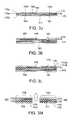
- the package portion 10includes a distribution layer 20 , a sealant 30 , an insulation layer 40 , a chip 50 , a plurality of internal wires 70 and a plurality of solder balls 90 .
- the sealant 30encapsulates the insulation layer 40 , the chip 50 and the internal wires 70 .
- the sealant 30is disposed on one side of the distribution layer 20 .
- the solder balls 90are disposed on the other side of the distribution layer 20 .
- the insulation layer 40is located between the distribution layer 20 and the chip 50 .
- One terminal of the internal wires 70is disposed on the chip 50 , and the other terminal of the internal wires 70 is connected to the distribution layer 20 .
- the chip 50is electrically connected to the solder balls 90 by the internal wires 70 via the distribution layer 20 .
- a thickness H 30 of the sealant 30is far larger than a thickness H 50 of the chip 50 , hence increasing the volume of the package portion 10 and restricting the miniaturization of electronic devices.
- a multi-function electronic deviceIn order to provide multiple functions, a multi-function electronic device must integrate a plurality of chips within. Thus, how to provide a package portion with increased packaging density and a method of manufacturing the same has become an important direction of the research and development in the semiconductor industry.
- the inventionis directed to a chip package structure and a method of manufacturing the same.
- the thickness of the sealant required by the package portionis reduced so that the density of the package structure is increased.
- a chip package structureincluding a package portion and a plurality of external conductors.
- the package portionincludes a distribution layer, a chip, a plurality internal conductors and a sealant.
- the distribution layerhas a first surface and a second surface, and the chip is disposed on the first surface.
- Each internal conductorhas a first terminal and a second terminal.
- the first terminalis disposed on the first surface.
- the sealantis disposed on the first surface for covering the chip and partly encapsulating the internal conductors, so that the first terminal and the second terminal of each internal conductor are exposed from the sealant.
- the external conductors disposed on the second surface of the distribution layer of the package portionare electrically connected to the internal conductors.
- a method of manufacturing chip package structureincludes the following steps: Firstly, a carrier having an adhering layer is provided. Next, a plurality internal conductors and at least one chip are disposed on the adhering layer, wherein each internal conductor has a first terminal and a second terminal, and the first terminal is disposed on the adhering layer. Then, a sealant is formed on the adhering layer to cover the chip and the internal conductors. Afterwards, the adhering layer is removed to expose the first terminal of each internal conductor, an active surface of the chip and a bottom surface of the sealant.
- a distribution layeris formed on the bottom surface of the sealant, so that the first terminal of each internal conductor and the active surface of the chip are disposed on a first surface of the distribution layer and electrically connected to the distribution layer to form a package portion, wherein the package portion includes the chip, the internal conductors corresponding to the chip, the distribution layer, and the sealant.
- a plurality of external conductorsis disposed on a second surface of the distribution layer.
- FIG. 1(Prior Art) shows a conventional chip package portion
- FIG. 2shows a chip package structure according to a first embodiment of the invention
- FIGS. 3A ⁇ 3Mshow a method of manufacturing the chip package structure of FIG. 2 ;
- FIG. 4shows a flowchart of the method of manufacturing the chip package structure in FIG. 2 ;
- FIG. 5shows two identical package portions stacked together
- FIG. 6shows two different package portions stacked together
- FIGS. 7A ⁇ 7Lshow a method of manufacturing the chip package structure according to a second embodiment of the invention.
- the chip package structureincludes a first package portion 100 and a plurality of first external conductors 130 .
- the first package portion 100includes a distribution layer 110 , a chip 150 , a plurality of internal conductors 170 and a sealant 190 .
- the distribution layer 110has a first surface 111 and a second surface 113 .
- the chip 150is disposed on the first surface 111 of the distribution layer 110 .
- the internal conductors 170has a first terminal 171 and a second terminal 273 , wherein the first terminal 171 is disposed on the first surface 111 of the distribution layer 110 .
- the sealant 190is disposed on the first surface 111 of the distribution layer 110 for covering the chip 150 and partly encapsulating the internal conductors 170 , so that the first terminal 171 and the second terminal 273 of each internal conductor 170 are exposed from the sealant 190 .
- the first external conductors 130 disposed on the second surface 113 of the distribution layer 110 of the first package portion 100are electrically connected to the internal conductors 170 .
- the first package portion 100further includes another distribution layer 210 disposed on the sealant 190 for covering the second terminal 273 of each internal conductor 170 .
- the required thickness of the sealant 190is reduced so that the volume of the first package portion 100 is decreased accordingly.
- FIGS. 3A ⁇ 3M and FIG. 4show a method of manufacturing the chip package structure of FIG. 2
- FIG. 4shows a flowchart of the method of manufacturing the chip package structure in FIG. 2 .
- the methodbegins at step 401 as indicated in FIG. 3A , a carrier 120 having an adhering layer 121 is provided.
- the carrier 120can be a metallic carrier, the surfaces 123 and 125 of the adhering layer 121 are both adhesive, and the surface 123 of the adhering layer 121 is adhered onto the carrier 120 .
- a plurality internal conductors 170 and at least one chipare disposed on the surface 125 of the adhering layer 121 .
- the chips 150 and 151substantially have the same structure.
- Each of the internal conductors 170has a first terminal 171 and a second terminal 173 , wherein the first terminal 171 of each internal conductor 170 and the chips 150 and 151 are adhered and fixed on the adhering layer 121 .
- a mold 220such as a plunger is provided to push the internal conductors 170 towards a direction D of the adhering layer 121 , so that the first terminal 171 of each internal conductor 170 is embedded into and fixed on the adhering layer 121 , but the mold 220 does not contact the chips 150 and 151 .
- the internal conductors 170will not move in subsequent processes.
- step 404a liquid encapsulating material 140 is spread on the adhering layer 121 , wherein the liquid encapsulating material 140 can flow on the adhering layer 121 .
- step 405as indicated in FIG. 3E , another mold 222 is provided to press and heat the liquid encapsulating material 140 (illustrated in FIG. 3D ) so that the liquid encapsulating material 140 solidifies as the sealant 190 .
- the sealant 190covers the chips 150 and 151 and the internal conductors 170 .
- the thickness H 190 of the sealant 190substantially is slightly larger than the thickness H 150 of the chips 150 and 151 , so that the sealant 190 covers the chips 150 and 151 and partly encapsulates the internal conductors 170 .
- the first terminal 171 of each internal conductor 170is embedded into the adhering layer 121 and exposed from the sealant 190 , but the second terminal 173 of each internal conductor 170 is encapsulated in the sealant 190 .
- step 406as indicated in FIG. 3F , a post-mold curing process is performed on the adhering layer 121 , and the adhering layer 121 and the sealant layer 190 are moved along a direction D 1 so that the adhering layer 121 comes off the carrier 120 .
- the sealant 190comes off the adhering layer 121 to expose the first terminal 171 of each internal conductor 170 , an active surface 150 ′ of the chips 150 and 151 , and a bottom surface of 190 ′ of the sealant 190 .
- a grinding tool 224is further provided to grind a top surface 191 of the sealant 190 until touching the second terminal 173 of each internal conductor 170 , and the internal conductors 170 are further grinded to expose a second terminal 273 having a larger area so that the electrical connection becomes more stable.
- the thickness H 191 of the sealant after grindingis still larger than the thickness H 150 of the chips 150 and 151 .
- step 408the sealant 190 is turned over to make the bottom surface 190 ′ and the active surface 150 ′ of the chips 150 and 151 face upwards, and the bottom surface 190 ′ of the sealant 190 forms a distribution layer 110 , so that the first terminal 171 of each internal conductor 170 and the active surface 150 ′ of the chips 150 and 151 are disposed on the first surface 111 of the distribution layer 110 and electrically connected to the distribution layer 110 .
- the first terminal 171 of each internal conductor 170is electrically connected to the chips 150 and 151 via the distribution layer 110 .
- the distribution layer 110includes an under bump metallurgy (UBM) 110 a , a re-distribution layer (RDL) 110 b and a polymer layer 110 c .
- the UBM 110 acontacts and makes the internal conductors 170 electrically connected to the re-distribution layer 110 b .
- the internal conductors 170are electrically connected to the chips 150 and 151 via the re-distribution layer 110 b .
- the polymer layer 110 cis used for electrical isolation purpose to avoid circuiting.
- the re-distribution layer 110 bcan be formed by way of sputtering, and the polymer layer 110 c can be pasted on the re-distribution layer 110 b.
- step 409the sealant 190 is turned over so that a grinded top surface 193 faces upwards and forms another distribution layer 210 .
- the distribution layer 210is electrically connected to the internal conductors 170 via the connection with the second terminal 273 of each internal conductor 170 .
- the formation of the distribution layer 210is the same with that of the distribution layer 110 , and is not repeated here.
- step 410as indicated in FIG. 3L , the sealant 190 is turned over, and the first external conductors 130 is disposed on the second surface 113 of the distribution layer 110 .
- the first external conductors 130contact the UBM 110 a or the re-distribution layer 110 b , so that the first external conductors 130 are electrically connected to the chips 150 and 151 via the internal conductors 170 and the distribution layer 110 .
- the methodproceeds to step 411 as indicated in FIG. 3M , the sealant 190 is turned over, and the sealant 190 and the distribution layers 110 and 210 are cut to form a plurality of first package portions 100 and 100 ′.
- the first package portion 100includes the chip 150 , the internal conductors 170 corresponding to the chip 150 , the distribution layers 110 and 210 , the sealant 190 and the first external conductors 130 .
- the first package portion 100 ′includes the chip 151 , the internal conductors 170 corresponding to the chip 151 , the distribution layers 110 and 210 , the sealant 190 and the first external conductors 130 .
- the chips 150 and 151 corresponding to the first package portions 100 and 100 ′are electrically connected to the active surface 150 ′ via the internal conductors 170 and the distribution layer 110 , and each of the chips 150 and 151 has an external conductor 130 and can be disposed on other electronic components.
- the chip package structure of the inventioncan be formed by stacking a plurality of package portions.
- the stacked package portionscan have the same or different structures.
- the first package portion 100 and the first package portion 100 ′have the same structure and the same size.
- the first external conductors 130 corresponding to the chip 151are connected to the distribution layer 210 of the first package portion 100 , so that the first package portion 100 and the first package portion 100 ′ are electrically connected together via the first external conductors 130 to form a stacked chip package structure.
- the first external conductor 130 of the first package portion 100 ′ disposed atopcan be directly connected to the internal conductor 170 of the first package portion 100 disposed underneath, hence omitting the distribution layer 210 of the first the package structure 100 .
- the first package portion 100 and the second package portion 300have different sizes and structures.
- a plurality of second external conductors 330 and the second package portion 300are disposed above the distribution layer 210 of the first package portion 100 , so that the second package portion 300 is electrically connected to the second terminal 273 of each internal conductor 170 via the second external conductors 330 .
- the second package portion 300further includes another chip 350 encapsulated by a sealant 390 .
- the chip 350is electrically connected to the second external conductors 330 .
- the chip 150 and the chip 350substantially have different structures.
- the second external conductors 330 contacting the distribution layer 210are electrically connected to the second terminal 273 of each internal conductor 170 via the distribution layer 210 , so that the chip 150 of the first package portion 100 and the chip 350 of the second package portion 300 which have different structures can be electrically connected together to form a stacked chip package structure.
- the chip package structure exemplified in the present embodiment of the inventioncan be used in a 3 dimensional fan-out wafer level chip scale package (WLCSP).
- the internal conductors 170 , the first external conductors 130 and the second external conductors 330can be a plurality of solder balls.
- There is no restriction about the shape and the size of the internal conductors 170and the thickness of each internal conductor 170 encapsulated by the sealant 190 is preferably slightly larger than the thickness H 150 of the chip 150 .
- the first package portion 100can reduce the required thickness of the sealant 190 and decrease the volume of the first package portion 100 .
- the second package portion 300is formed on the sealant 190 via the distribution layer 210 of the first package portion 100 for electrically connecting the two package portions.
- the second external conductors 330do not need to correspond to the internal conductors 170 , and the second package portion 300 can have any size or shape, hence increasing the adaptability of the chip package structure.
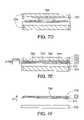
- FIGS. 7A ⁇ 7La method of manufacturing the chip package structure according to a second embodiment of the invention is shown.
- a metallic carrier 720 having an adhering layer 721 disposed thereonis provided.
- the surfaces 723 and 725 of the adhering layer 721are both adhesive, and the surface 723 of the adhering layer 721 is adhered on the metallic carrier 720 .
- the surface 725 of the adhering layer 721forms a plurality internal conductors 770 and at least one chip.
- two chips 750 and 751are used.
- the chips 750 and 751substantially have the same structure.
- the internal conductors 770are respectively disposed on the two sides of the chips 750 and 751 .
- Each internal conductor 770has a first terminal 771 and a second terminal 773 , and the first terminal 771 is disposed on the adhering layer 721 .
- a plunger 722is provided to push the internal conductors 770 towards a direction D of the adhering layer 721 , so that the first terminal 771 of each internal conductor 770 is embedded into and fixed on the adhering layer 721 .
- the plunger 722does not contact the chips 750 and 751 .
- a liquid encapsulating material 740is spread on the adhering layer 721 , and a mold 724 is provided.
- the liquid encapsulating material 740can flow on the adhering layer 721 .
- the mold 724has another adhering layer 727 .
- the mold 724is used to press and heat the liquid encapsulating material 740 (illustrated in FIG. 7D ), so that the second terminal 773 of each internal conductor 770 is embedded into the adhering layer 727 .
- the first terminal 771 of each internal conductor 770can be concurrently embedded into the adhering layer 721 .
- the liquid encapsulating material 740is pressed and heated by the mold 724 and solidifies to be the sealant 790 for covering the chips 750 and 751 and internal conductors 770 .
- a thickness H 790 of the sealant 790is substantially slightly larger than a thickness H 750 of the chips 750 and 751 , so that the sealant 790 covers the chips 750 and 751 and partly encapsulates the internal conductors 770 .
- the first terminal 771 and the second terminal 773 of each internal conductor 770are exposed from the sealant 790 .
- a post-mold curing processis performed on the adhering layer 721 , and the adhering layer 721 and the sealant layer 790 are removed along the direction D 1 so that the adhering layer 721 comes off the metallic carrier 720 .
- the adhering layer 727is also removed along with the mold 724 to expose the second terminal 773 of each internal conductor 770 .
- the adhering layer 721is removed to expose the first terminal 771 of each internal conductor 770 , an active surface 750 ′ of the chips 750 and 751 , and a bottom surface of 790 ′ of the sealant 790 .
- the sealant 790is turned over and makes the bottom surface 790 ′ of the sealant 790 and the active surface 750 ′ of the chips 750 and 751 face upwards, and the bottom surface 790 ′ of the sealant 790 forms the distribution layer 710 , so that the first terminal 771 of each internal conductor 770 and the chips 750 and 751 are disposed on a first surface of 711 of the distribution layer 710 and electrically connected to the distribution layer 710 .
- the internal conductors 770 disposed on two sides of the chips 750 and 751are respectively electrically connected to the corresponding chips 750 and 751 by connecting the first terminal 771 to the distribution layer 110 .
- the sealant 790is turned over so that a top surface 793 of the sealant 790 faces upwards and forms another distribution layer 715 .
- the distribution layer 715is electrically connected to the internal conductors 770 and the chips 750 and 751 via the connection with the second terminal 773 of each internal conductor 770 .
- the sealant layer 790is turned over so that the distribution layer 710 face upwards and a plurality of first external conductors 730 are disposed on a second surface of 713 of the distribution layer 710 .
- the first external conductors 730are electrically connected to the chips 750 and 751 via the internal conductors 770 and the distribution layer 710 .
- the first package portion 950includes the chip 750 , the internal conductors corresponding to the chip 750 , and the first external conductors.
- the first package portion 950 ′includes the chip 751 , the internal conductors corresponding to the chip 751 , and the first external conductors.
- the first package portion 950 ′is disposed on the first package portion 950 to form a stackable chip package structure.
- the second terminal 773 of each internal conductor 770is embedded into the adhering layer 727 . After the adhering layer 727 is removed, the first terminal 771 and the second terminal 773 of each internal conductor 770 are exposed from the sealant 790 .
- the chip package structurecan form the distribution layers 710 and 715 without going through the grinding process, hence saving the grinding material and simplifying the method of manufacturing the chip package structure.
- the manufacturing method of the inventioncan form one package portion, three package portions, ten package portions or even more package portions.
- the required thickness of package portionsis reduced, and the package portions of different types can be stacked via the distribution layer.
- the volume of the chip package structure of the inventionis five to six times smaller than that of multi-chip module (MCM) package structure.
- MCMmulti-chip module
- the chip package structure disclosed in the preferred embodiments of the inventioncan be used in flash random-access memory (RAM), static random-access memory (SRAM), dynamic random-access memory (DRAM), processor, application specific integrated circuit (ASIC) or controller.
- each package portioncan be inspected before stacking so that the properties of each package portion can be inspected earlier.
Landscapes
- Engineering & Computer Science (AREA)
- Power Engineering (AREA)
- Microelectronics & Electronic Packaging (AREA)
- Computer Hardware Design (AREA)
- Physics & Mathematics (AREA)
- Condensed Matter Physics & Semiconductors (AREA)
- General Physics & Mathematics (AREA)
- Manufacturing & Machinery (AREA)
- Structures Or Materials For Encapsulating Or Coating Semiconductor Devices Or Solid State Devices (AREA)
Abstract
Description
- This application claims the benefit of Taiwan application Ser. No. 9,613,9548, filed Oct, 22, 2007, the subject matter of which is incorporated herein by reference.
- 1. Field of the Invention
- The invention relates in general to a package structure and a method of manufacturing the same, and more particularly to a chip package structure and a method of manufacturing the same.
- 2. Description of the Related Art
- In recent years, electronic devices have been widely used in people's everyday life, and the manufacturers are dedicated to the development of miniaturized and multi-function electronic products to meet the market demands. Among the package structures used in the semiconductor components of electronic products, the wafer level chip scale package (WLCSP) is the most commonly used package structure.
- Referring to
FIG. 1 , a conventional chip package portion is shown. Thepackage portion 10 includes adistribution layer 20, asealant 30, aninsulation layer 40, achip 50, a plurality ofinternal wires 70 and a plurality ofsolder balls 90. Thesealant 30 encapsulates theinsulation layer 40, thechip 50 and theinternal wires 70. Thesealant 30 is disposed on one side of thedistribution layer 20. Thesolder balls 90 are disposed on the other side of thedistribution layer 20. Theinsulation layer 40 is located between thedistribution layer 20 and thechip 50. One terminal of theinternal wires 70 is disposed on thechip 50, and the other terminal of theinternal wires 70 is connected to thedistribution layer 20. Thechip 50 is electrically connected to thesolder balls 90 by theinternal wires 70 via thedistribution layer 20. - Due to the restriction on the shape of the
internal wires 70, a thickness H30 of thesealant 30 is far larger than a thickness H50 of thechip 50, hence increasing the volume of thepackage portion 10 and restricting the miniaturization of electronic devices. In order to provide multiple functions, a multi-function electronic device must integrate a plurality of chips within. Thus, how to provide a package portion with increased packaging density and a method of manufacturing the same has become an important direction of the research and development in the semiconductor industry. - The invention is directed to a chip package structure and a method of manufacturing the same. By using the design of each internal conductor and corresponding external conductors, the thickness of the sealant required by the package portion is reduced so that the density of the package structure is increased.
- According to a first aspect of the present invention, a chip package structure including a package portion and a plurality of external conductors is provided. The package portion includes a distribution layer, a chip, a plurality internal conductors and a sealant. The distribution layer has a first surface and a second surface, and the chip is disposed on the first surface. Each internal conductor has a first terminal and a second terminal. The first terminal is disposed on the first surface. The sealant is disposed on the first surface for covering the chip and partly encapsulating the internal conductors, so that the first terminal and the second terminal of each internal conductor are exposed from the sealant. The external conductors disposed on the second surface of the distribution layer of the package portion are electrically connected to the internal conductors.
- According to a second aspect of the present invention, a method of manufacturing chip package structure is provided. The manufacturing method includes the following steps: Firstly, a carrier having an adhering layer is provided. Next, a plurality internal conductors and at least one chip are disposed on the adhering layer, wherein each internal conductor has a first terminal and a second terminal, and the first terminal is disposed on the adhering layer. Then, a sealant is formed on the adhering layer to cover the chip and the internal conductors. Afterwards, the adhering layer is removed to expose the first terminal of each internal conductor, an active surface of the chip and a bottom surface of the sealant. In addition, a distribution layer is formed on the bottom surface of the sealant, so that the first terminal of each internal conductor and the active surface of the chip are disposed on a first surface of the distribution layer and electrically connected to the distribution layer to form a package portion, wherein the package portion includes the chip, the internal conductors corresponding to the chip, the distribution layer, and the sealant. Lastly, a plurality of external conductors is disposed on a second surface of the distribution layer.
- The invention will become apparent from the following detailed description of the preferred but non-limiting embodiments. The following description is made with reference to the accompanying drawings.
FIG. 1 (Prior Art) shows a conventional chip package portion;FIG. 2 shows a chip package structure according to a first embodiment of the invention;FIGS. 3A˜3M show a method of manufacturing the chip package structure ofFIG. 2 ;FIG. 4 shows a flowchart of the method of manufacturing the chip package structure inFIG. 2 ;FIG. 5 shows two identical package portions stacked together;FIG. 6 shows two different package portions stacked together; andFIGS. 7A˜7L show a method of manufacturing the chip package structure according to a second embodiment of the invention.- Referring to
FIG. 2 , a chip package structure according to a first embodiment of the invention is shown. The chip package structure includes afirst package portion 100 and a plurality of firstexternal conductors 130. Thefirst package portion 100 includes adistribution layer 110, achip 150, a plurality ofinternal conductors 170 and asealant 190. - The
distribution layer 110 has afirst surface 111 and asecond surface 113. Thechip 150 is disposed on thefirst surface 111 of thedistribution layer 110. Theinternal conductors 170 has afirst terminal 171 and asecond terminal 273, wherein thefirst terminal 171 is disposed on thefirst surface 111 of thedistribution layer 110. Thesealant 190 is disposed on thefirst surface 111 of thedistribution layer 110 for covering thechip 150 and partly encapsulating theinternal conductors 170, so that thefirst terminal 171 and thesecond terminal 273 of eachinternal conductor 170 are exposed from thesealant 190. The firstexternal conductors 130 disposed on thesecond surface 113 of thedistribution layer 110 of thefirst package portion 100 are electrically connected to theinternal conductors 170. - The
first package portion 100 further includes anotherdistribution layer 210 disposed on thesealant 190 for covering thesecond terminal 273 of eachinternal conductor 170. With the disposition of theinternal conductors 170 whose thickness is slightly larger than the thickness ofchip 150, the required thickness of thesealant 190 is reduced so that the volume of thefirst package portion 100 is decreased accordingly. - Referring to
FIGS. 3A˜3M andFIG. 4 ,FIGS. 3A˜3M show a method of manufacturing the chip package structure ofFIG. 2 , andFIG. 4 shows a flowchart of the method of manufacturing the chip package structure inFIG. 2 . - The method begins at
step 401 as indicated inFIG. 3A , acarrier 120 having an adheringlayer 121 is provided. Thecarrier 120 can be a metallic carrier, thesurfaces layer 121 are both adhesive, and thesurface 123 of the adheringlayer 121 is adhered onto thecarrier 120. - Next, the method proceeds to step402 as indicated in
FIG. 3B , a pluralityinternal conductors 170 and at least one chip are disposed on thesurface 125 of the adheringlayer 121. In the present embodiment of the invention, thechips internal conductors 170 has afirst terminal 171 and asecond terminal 173, wherein thefirst terminal 171 of eachinternal conductor 170 and thechips layer 121. - Then, the method proceeds to step403 as indicated in
FIG. 3C , amold 220 such as a plunger is provided to push theinternal conductors 170 towards a direction D of the adheringlayer 121, so that thefirst terminal 171 of eachinternal conductor 170 is embedded into and fixed on the adheringlayer 121, but themold 220 does not contact thechips internal conductors 170 are pushed into the adheringlayer 121, theinternal conductors 170 will not move in subsequent processes. - Then, the method proceeds to step404 as indicated in
FIG. 3D , aliquid encapsulating material 140 is spread on the adheringlayer 121, wherein theliquid encapsulating material 140 can flow on the adheringlayer 121. - Then, the method proceeds to step405 as indicated in
FIG. 3E , anothermold 222 is provided to press and heat the liquid encapsulating material140 (illustrated inFIG. 3D ) so that theliquid encapsulating material 140 solidifies as thesealant 190. Thesealant 190 covers thechips internal conductors 170. The thickness H190 of thesealant 190 substantially is slightly larger than the thickness H150 of thechips sealant 190 covers thechips internal conductors 170. Thefirst terminal 171 of eachinternal conductor 170 is embedded into the adheringlayer 121 and exposed from thesealant 190, but thesecond terminal 173 of eachinternal conductor 170 is encapsulated in thesealant 190. - Afterwards, the method proceeds to step406 as indicated in
FIG. 3F , a post-mold curing process is performed on the adheringlayer 121, and the adheringlayer 121 and thesealant layer 190 are moved along a direction D1 so that the adheringlayer 121 comes off thecarrier 120. Next, as indicated inFIG. 3G , thesealant 190 comes off the adheringlayer 121 to expose thefirst terminal 171 of eachinternal conductor 170, anactive surface 150′ of thechips sealant 190. - Next, the method proceeds to step407 as indicted in
FIGS. 3H and 3I , a grindingtool 224 is further provided to grind atop surface 191 of thesealant 190 until touching thesecond terminal 173 of eachinternal conductor 170, and theinternal conductors 170 are further grinded to expose asecond terminal 273 having a larger area so that the electrical connection becomes more stable. The thickness H191 of the sealant after grinding is still larger than the thickness H150 of thechips - Next, the method proceeds to step408 as indicted in
FIG. 3J , thesealant 190 is turned over to make thebottom surface 190′ and theactive surface 150′ of thechips bottom surface 190′ of thesealant 190 forms adistribution layer 110, so that thefirst terminal 171 of eachinternal conductor 170 and theactive surface 150′ of thechips first surface 111 of thedistribution layer 110 and electrically connected to thedistribution layer 110. Thefirst terminal 171 of eachinternal conductor 170 is electrically connected to thechips distribution layer 110. - The
distribution layer 110 includes an under bump metallurgy (UBM)110a, a re-distribution layer (RDL)110band apolymer layer 110c. TheUBM 110acontacts and makes theinternal conductors 170 electrically connected to there-distribution layer 110b. Theinternal conductors 170 are electrically connected to thechips re-distribution layer 110b. Thepolymer layer 110cis used for electrical isolation purpose to avoid circuiting. There-distribution layer 110bcan be formed by way of sputtering, and thepolymer layer 110ccan be pasted on there-distribution layer 110b. - Then, the method proceeds to step409 as indicated in
FIG. 3K , thesealant 190 is turned over so that a grindedtop surface 193 faces upwards and forms anotherdistribution layer 210. Thedistribution layer 210 is electrically connected to theinternal conductors 170 via the connection with thesecond terminal 273 of eachinternal conductor 170. The formation of thedistribution layer 210 is the same with that of thedistribution layer 110, and is not repeated here. - Then, the method proceeds to step410 as indicated in
FIG. 3L , thesealant 190 is turned over, and the firstexternal conductors 130 is disposed on thesecond surface 113 of thedistribution layer 110. The firstexternal conductors 130 contact theUBM 110aor there-distribution layer 110b, so that the firstexternal conductors 130 are electrically connected to thechips internal conductors 170 and thedistribution layer 110. - Then, the method proceeds to step411 as indicated in
FIG. 3M , thesealant 190 is turned over, and thesealant 190 and the distribution layers110 and210 are cut to form a plurality offirst package portions first package portion 100 includes thechip 150, theinternal conductors 170 corresponding to thechip 150, the distribution layers110 and210, thesealant 190 and the firstexternal conductors 130. Thefirst package portion 100′ includes thechip 151, theinternal conductors 170 corresponding to thechip 151, the distribution layers110 and210, thesealant 190 and the firstexternal conductors 130. - For the chip package structure which is manufactured according to the above method, the
chips first package portions active surface 150′ via theinternal conductors 170 and thedistribution layer 110, and each of thechips external conductor 130 and can be disposed on other electronic components. - Further, the chip package structure of the invention can be formed by stacking a plurality of package portions. The stacked package portions can have the same or different structures.
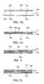
- Referring to
FIG. 5 , two identical package portions stacked together is shown. Thefirst package portion 100 and thefirst package portion 100′ have the same structure and the same size. The firstexternal conductors 130 corresponding to thechip 151 are connected to thedistribution layer 210 of thefirst package portion 100, so that thefirst package portion 100 and thefirst package portion 100′ are electrically connected together via the firstexternal conductors 130 to form a stacked chip package structure. Moreover, if the stacked package structure is formed by stacking over two identical package portions, the firstexternal conductor 130 of thefirst package portion 100′ disposed atop can be directly connected to theinternal conductor 170 of thefirst package portion 100 disposed underneath, hence omitting thedistribution layer 210 of the first thepackage structure 100. - Referring to
FIG. 6 , two different package portions stacked together is shown. Thefirst package portion 100 and thesecond package portion 300 have different sizes and structures. A plurality of secondexternal conductors 330 and thesecond package portion 300 are disposed above thedistribution layer 210 of thefirst package portion 100, so that thesecond package portion 300 is electrically connected to thesecond terminal 273 of eachinternal conductor 170 via the secondexternal conductors 330. Thesecond package portion 300 further includes anotherchip 350 encapsulated by asealant 390. Thechip 350 is electrically connected to the secondexternal conductors 330. Thechip 150 and thechip 350 substantially have different structures. The secondexternal conductors 330 contacting thedistribution layer 210 are electrically connected to thesecond terminal 273 of eachinternal conductor 170 via thedistribution layer 210, so that thechip 150 of thefirst package portion 100 and thechip 350 of thesecond package portion 300 which have different structures can be electrically connected together to form a stacked chip package structure. - The chip package structure exemplified in the present embodiment of the invention can be used in a 3 dimensional fan-out wafer level chip scale package (WLCSP). The
internal conductors 170, the firstexternal conductors 130 and the secondexternal conductors 330 can be a plurality of solder balls. There is no restriction about the shape and the size of theinternal conductors 170, and the thickness of eachinternal conductor 170 encapsulated by thesealant 190 is preferably slightly larger than the thickness H150 of thechip 150. With the disposition of theinternal conductors 170, thefirst package portion 100 can reduce the required thickness of thesealant 190 and decrease the volume of thefirst package portion 100. When the chip package structure is formed by stacking different package portions, thesecond package portion 300 is formed on thesealant 190 via thedistribution layer 210 of thefirst package portion 100 for electrically connecting the two package portions. Thus, the secondexternal conductors 330 do not need to correspond to theinternal conductors 170, and thesecond package portion 300 can have any size or shape, hence increasing the adaptability of the chip package structure. - Referring to
FIGS. 7A˜7L , a method of manufacturing the chip package structure according to a second embodiment of the invention is shown. - As indicated in
FIG. 7A , ametallic carrier 720 having an adheringlayer 721 disposed thereon is provided. Thesurfaces layer 721 are both adhesive, and thesurface 723 of the adheringlayer 721 is adhered on themetallic carrier 720. - As indicated in
FIG. 7B , thesurface 725 of the adheringlayer 721 forms a pluralityinternal conductors 770 and at least one chip. In the present embodiment of the invention, twochips chips internal conductors 770 are respectively disposed on the two sides of thechips internal conductor 770 has afirst terminal 771 and asecond terminal 773, and thefirst terminal 771 is disposed on the adheringlayer 721. - Next, as indicated in
FIG. 7C , aplunger 722 is provided to push theinternal conductors 770 towards a direction D of the adheringlayer 721, so that thefirst terminal 771 of eachinternal conductor 770 is embedded into and fixed on the adheringlayer 721. Theplunger 722 does not contact thechips - Then, as indicated in
FIG. 7D , aliquid encapsulating material 740 is spread on the adheringlayer 721, and amold 724 is provided. Theliquid encapsulating material 740 can flow on the adheringlayer 721. Themold 724 has another adheringlayer 727. - Afterwards, as indicated in
FIG. 7E , themold 724 is used to press and heat the liquid encapsulating material740 (illustrated inFIG. 7D ), so that thesecond terminal 773 of eachinternal conductor 770 is embedded into the adheringlayer 727. Thefirst terminal 771 of eachinternal conductor 770 can be concurrently embedded into the adheringlayer 721. Theliquid encapsulating material 740 is pressed and heated by themold 724 and solidifies to be thesealant 790 for covering thechips internal conductors 770. A thickness H790 of thesealant 790 is substantially slightly larger than a thickness H750 of thechips sealant 790 covers thechips internal conductors 770. Thefirst terminal 771 and thesecond terminal 773 of eachinternal conductor 770 are exposed from thesealant 790. - Then, as indicated in
FIG. 7F , a post-mold curing process is performed on the adheringlayer 721, and the adheringlayer 721 and thesealant layer 790 are removed along the direction D1 so that the adheringlayer 721 comes off themetallic carrier 720. The adheringlayer 727 is also removed along with themold 724 to expose thesecond terminal 773 of eachinternal conductor 770. - Next, as indicated in
FIG. 7G , the adheringlayer 721 is removed to expose thefirst terminal 771 of eachinternal conductor 770, anactive surface 750′ of thechips sealant 790. - After that, as indicated in
FIG. 7H , thesealant 790 is turned over and makes thebottom surface 790′ of thesealant 790 and theactive surface 750′ of thechips bottom surface 790′ of thesealant 790 forms thedistribution layer 710, so that thefirst terminal 771 of eachinternal conductor 770 and thechips distribution layer 710 and electrically connected to thedistribution layer 710. Theinternal conductors 770 disposed on two sides of thechips chips first terminal 771 to thedistribution layer 110. - Then, as indicated in
FIG. 71 , thesealant 790 is turned over so that atop surface 793 of thesealant 790 faces upwards and forms anotherdistribution layer 715. Thedistribution layer 715 is electrically connected to theinternal conductors 770 and thechips second terminal 773 of eachinternal conductor 770. - Afterwards, as indicated in
FIG. 7J , thesealant layer 790 is turned over so that thedistribution layer 710 face upwards and a plurality of firstexternal conductors 730 are disposed on a second surface of713 of thedistribution layer 710. The firstexternal conductors 730 are electrically connected to thechips internal conductors 770 and thedistribution layer 710. - Then, as indicated in
FIG. 7K , thesealant 790 and the distribution layers710 and715 are cut to form a plurality offirst package portions first package portion 950 includes thechip 750, the internal conductors corresponding to thechip 750, and the first external conductors. Thefirst package portion 950′ includes thechip 751, the internal conductors corresponding to thechip 751, and the first external conductors. - Next, as indicated in
FIG. 7L , thefirst package portion 950′ is disposed on thefirst package portion 950 to form a stackable chip package structure. - For the chip package structure disclosed in the present embodiment of the invention, the
second terminal 773 of eachinternal conductor 770 is embedded into the adheringlayer 727. After the adheringlayer 727 is removed, thefirst terminal 771 and thesecond terminal 773 of eachinternal conductor 770 are exposed from thesealant 790. Thus, the chip package structure can form the distribution layers710 and715 without going through the grinding process, hence saving the grinding material and simplifying the method of manufacturing the chip package structure. - Despite the method of manufacturing the chip package structure is exemplified by forming two package portions at a time, anyone who is skilled in the technology of the invention will understand that the quantity of package portions is not for limiting the scope of protection of the invention. The manufacturing method of the invention can form one package portion, three package portions, ten package portions or even more package portions.
- According to the chip package structure and the method of manufacturing the same disclosed in the above embodiments of the invention, the required thickness of package portions is reduced, and the package portions of different types can be stacked via the distribution layer. Thus, the volume of the chip package structure of the invention is five to six times smaller than that of multi-chip module (MCM) package structure. The chip package structure disclosed in the preferred embodiments of the invention can be used in flash random-access memory (RAM), static random-access memory (SRAM), dynamic random-access memory (DRAM), processor, application specific integrated circuit (ASIC) or controller. In addition, each package portion can be inspected before stacking so that the properties of each package portion can be inspected earlier.
- While the invention has been described by way of example and in terms of a preferred embodiment, it is to be understood that the invention is not limited thereto. On the contrary, it is intended to cover various modifications and similar arrangements and procedures, and the scope of the appended claims therefore should be accorded the broadest interpretation so as to encompass all such modifications and similar arrangements and procedures.
Claims (20)
Applications Claiming Priority (3)
| Application Number | Priority Date | Filing Date | Title |
|---|---|---|---|
| TW96139548 | 2007-10-22 | ||
| TW096139548ATWI360207B (en) | 2007-10-22 | 2007-10-22 | Chip package structure and method of manufacturing |
| TW96139548A | 2007-10-22 |
Publications (2)
| Publication Number | Publication Date |
|---|---|
| US20090102066A1true US20090102066A1 (en) | 2009-04-23 |
| US8035213B2 US8035213B2 (en) | 2011-10-11 |
Family
ID=40562664
Family Applications (1)
| Application Number | Title | Priority Date | Filing Date |
|---|---|---|---|
| US12/285,268Active2028-10-16US8035213B2 (en) | 2007-10-22 | 2008-10-01 | Chip package structure and method of manufacturing the same |
Country Status (2)
| Country | Link |
|---|---|
| US (1) | US8035213B2 (en) |
| TW (1) | TWI360207B (en) |
Cited By (20)
| Publication number | Priority date | Publication date | Assignee | Title |
|---|---|---|---|---|
| US20100320593A1 (en)* | 2009-06-19 | 2010-12-23 | Advanced Semiconductor Engineering, Inc. | Chip Package Structure and Manufacturing Methods Thereof |
| US20110018118A1 (en)* | 2009-07-21 | 2011-01-27 | Advanced Semiconductor Engineering, Inc. | Semiconductor Device Packages, Redistribution Structures, and Manufacturing Methods Thereof |
| US20110018124A1 (en)* | 2009-07-23 | 2011-01-27 | Advanced Semiconductor Engineering, Inc. | Semiconductor Device Packages, Redistribution Structures, and Manufacturing Methods Thereof |
| US20110084372A1 (en)* | 2009-10-14 | 2011-04-14 | Advanced Semiconductor Engineering, Inc. | Package carrier, semiconductor package, and process for fabricating same |
| US20110115060A1 (en)* | 2009-11-19 | 2011-05-19 | Advanced Semiconductor Engineering, Inc. | Wafer-Level Semiconductor Device Packages with Electromagnetic Interference Shielding |
| US20110127654A1 (en)* | 2009-11-27 | 2011-06-02 | Advanced Semiconductor Engineering, Inc.., | Semiconductor Package and Manufacturing Methods Thereof |
| US20110169150A1 (en)* | 2010-01-13 | 2011-07-14 | Advanced Semiconductor Engineering, Inc. | Semiconductor Package with Single Sided Substrate Design and Manufacturing Methods Thereof |
| US20110177654A1 (en)* | 2010-01-21 | 2011-07-21 | Advanced Semiconductor Engineering, Inc. | Wafer-Level Semiconductor Device Packages with Three-Dimensional Fan-Out and Manufacturing Methods Thereof |
| US20110194265A1 (en)* | 2010-02-05 | 2011-08-11 | Advanced Semiconductor Engineering, Inc. | Embedded Component Substrate and Manufacturing Methods Thereof |
| US20110227220A1 (en)* | 2010-03-22 | 2011-09-22 | Chia-Ching Chen | Stackable semiconductor package and manufacturing method thereof |
| US8035213B2 (en)* | 2007-10-22 | 2011-10-11 | Advanced Semiconductor Engineering, Inc. | Chip package structure and method of manufacturing the same |
| US20120074567A1 (en)* | 2009-06-12 | 2012-03-29 | Stats Chippac, Ltd. | Semiconductor Device and Method of Forming Vertical Interconnect Structure Between Non-Linear Portions of Conductive Layers |
| US8278746B2 (en) | 2010-04-02 | 2012-10-02 | Advanced Semiconductor Engineering, Inc. | Semiconductor device packages including connecting elements |
| US8624374B2 (en) | 2010-04-02 | 2014-01-07 | Advanced Semiconductor Engineering, Inc. | Semiconductor device packages with fan-out and with connecting elements for stacking and manufacturing methods thereof |
| US20140177193A1 (en)* | 2012-12-21 | 2014-06-26 | Liwen Jin | Bumpless build-up layer package including a release layer |
| US8941222B2 (en) | 2010-11-11 | 2015-01-27 | Advanced Semiconductor Engineering Inc. | Wafer level semiconductor package and manufacturing methods thereof |
| US9406658B2 (en) | 2010-12-17 | 2016-08-02 | Advanced Semiconductor Engineering, Inc. | Embedded component device and manufacturing methods thereof |
| US10236245B2 (en)* | 2016-03-23 | 2019-03-19 | Dyi-chung Hu | Package substrate with embedded circuit |
| IT201800002903A1 (en)* | 2018-02-21 | 2019-08-21 | St Microelectronics Srl | PROCEDURE FOR MANUFACTURING SEMICONDUCTOR DEVICES AND CORRESPONDING SEMICONDUCTOR DEVICE |
| WO2020103747A1 (en)* | 2018-11-20 | 2020-05-28 | 苏州晶方半导体科技股份有限公司 | Chip packaging structure |
Families Citing this family (56)
| Publication number | Priority date | Publication date | Assignee | Title |
|---|---|---|---|---|
| KR101313391B1 (en) | 2004-11-03 | 2013-10-01 | 테세라, 인코포레이티드 | Stacked packaging improvements |
| US8058101B2 (en) | 2005-12-23 | 2011-11-15 | Tessera, Inc. | Microelectronic packages and methods therefor |
| TWI455215B (en)* | 2009-06-11 | 2014-10-01 | Advanced Semiconductor Eng | Semiconductor package and manufacturing method thereof |
| US8884422B2 (en)* | 2009-12-31 | 2014-11-11 | Stmicroelectronics Pte Ltd. | Flip-chip fan-out wafer level package for package-on-package applications, and method of manufacture |
| US9159708B2 (en) | 2010-07-19 | 2015-10-13 | Tessera, Inc. | Stackable molded microelectronic packages with area array unit connectors |
| US8482111B2 (en) | 2010-07-19 | 2013-07-09 | Tessera, Inc. | Stackable molded microelectronic packages |
| US8337657B1 (en)* | 2010-10-27 | 2012-12-25 | Amkor Technology, Inc. | Mechanical tape separation package and method |
| US20120146206A1 (en)* | 2010-12-13 | 2012-06-14 | Tessera Research Llc | Pin attachment |
| US8618659B2 (en) | 2011-05-03 | 2013-12-31 | Tessera, Inc. | Package-on-package assembly with wire bonds to encapsulation surface |
| KR101128063B1 (en) | 2011-05-03 | 2012-04-23 | 테세라, 인코포레이티드 | Package-on-package assembly with wire bonds to encapsulation surface |
| US9013037B2 (en) | 2011-09-14 | 2015-04-21 | Stmicroelectronics Pte Ltd. | Semiconductor package with improved pillar bump process and structure |
| US8836136B2 (en) | 2011-10-17 | 2014-09-16 | Invensas Corporation | Package-on-package assembly with wire bond vias |
| US8779601B2 (en)* | 2011-11-02 | 2014-07-15 | Stmicroelectronics Pte Ltd | Embedded wafer level package for 3D and package-on-package applications, and method of manufacture |
| US8916481B2 (en) | 2011-11-02 | 2014-12-23 | Stmicroelectronics Pte Ltd. | Embedded wafer level package for 3D and package-on-package applications, and method of manufacture |
| US8946757B2 (en) | 2012-02-17 | 2015-02-03 | Invensas Corporation | Heat spreading substrate with embedded interconnects |
| US8372741B1 (en) | 2012-02-24 | 2013-02-12 | Invensas Corporation | Method for package-on-package assembly with wire bonds to encapsulation surface |
| US9082780B2 (en)* | 2012-03-23 | 2015-07-14 | Stats Chippac, Ltd. | Semiconductor device and method of forming a robust fan-out package including vertical interconnects and mechanical support layer |
| US8835228B2 (en) | 2012-05-22 | 2014-09-16 | Invensas Corporation | Substrate-less stackable package with wire-bond interconnect |
| US9391008B2 (en) | 2012-07-31 | 2016-07-12 | Invensas Corporation | Reconstituted wafer-level package DRAM |
| US9502390B2 (en) | 2012-08-03 | 2016-11-22 | Invensas Corporation | BVA interposer |
| US9799592B2 (en)* | 2013-11-19 | 2017-10-24 | Amkor Technology, Inc. | Semicondutor device with through-silicon via-less deep wells |
| US8878353B2 (en) | 2012-12-20 | 2014-11-04 | Invensas Corporation | Structure for microelectronic packaging with bond elements to encapsulation surface |
| US9455160B2 (en)* | 2013-01-14 | 2016-09-27 | Infineon Technologies Ag | Method for fabricating a semiconductor chip panel |
| US8778738B1 (en) | 2013-02-19 | 2014-07-15 | Taiwan Semiconductor Manufacturing Company, Ltd. | Packaged semiconductor devices and packaging devices and methods |
| US9953907B2 (en) | 2013-01-29 | 2018-04-24 | Taiwan Semiconductor Manufacturing Company, Ltd. | PoP device |
| US20140210106A1 (en)* | 2013-01-29 | 2014-07-31 | Apple Inc. | ULTRA THIN PoP PACKAGE |
| US9136254B2 (en) | 2013-02-01 | 2015-09-15 | Invensas Corporation | Microelectronic package having wire bond vias and stiffening layer |
| TWI515808B (en)* | 2013-04-25 | 2016-01-01 | 南茂科技股份有限公司 | Method for manufacturing chip package structure |
| US9167710B2 (en) | 2013-08-07 | 2015-10-20 | Invensas Corporation | Embedded packaging with preformed vias |
| US9685365B2 (en) | 2013-08-08 | 2017-06-20 | Invensas Corporation | Method of forming a wire bond having a free end |
| US20150076714A1 (en) | 2013-09-16 | 2015-03-19 | Invensas Corporation | Microelectronic element with bond elements to encapsulation surface |
| US9368375B2 (en) | 2013-10-11 | 2016-06-14 | Taiwan Semiconductor Manufacturing Company, Ltd. | Apparatus and method for self-aligning chip placement and leveling |
| US9093449B2 (en)* | 2013-10-23 | 2015-07-28 | Taiwan Semiconductor Manufacturing Company, Ltd. | Apparatus and method for chip placement and molding |
| US9379074B2 (en) | 2013-11-22 | 2016-06-28 | Invensas Corporation | Die stacks with one or more bond via arrays of wire bond wires and with one or more arrays of bump interconnects |
| US9263394B2 (en) | 2013-11-22 | 2016-02-16 | Invensas Corporation | Multiple bond via arrays of different wire heights on a same substrate |
| US9583456B2 (en) | 2013-11-22 | 2017-02-28 | Invensas Corporation | Multiple bond via arrays of different wire heights on a same substrate |
| US9583411B2 (en) | 2014-01-17 | 2017-02-28 | Invensas Corporation | Fine pitch BVA using reconstituted wafer with area array accessible for testing |
| CN104882386B (en)* | 2014-02-27 | 2019-03-01 | 恩智浦美国有限公司 | Semiconductor devices grid array package |
| US10381326B2 (en) | 2014-05-28 | 2019-08-13 | Invensas Corporation | Structure and method for integrated circuits packaging with increased density |
| US9646917B2 (en) | 2014-05-29 | 2017-05-09 | Invensas Corporation | Low CTE component with wire bond interconnects |
| US9412714B2 (en) | 2014-05-30 | 2016-08-09 | Invensas Corporation | Wire bond support structure and microelectronic package including wire bonds therefrom |
| US9735084B2 (en) | 2014-12-11 | 2017-08-15 | Invensas Corporation | Bond via array for thermal conductivity |
| US9888579B2 (en) | 2015-03-05 | 2018-02-06 | Invensas Corporation | Pressing of wire bond wire tips to provide bent-over tips |
| US9502372B1 (en) | 2015-04-30 | 2016-11-22 | Invensas Corporation | Wafer-level packaging using wire bond wires in place of a redistribution layer |
| US9761554B2 (en) | 2015-05-07 | 2017-09-12 | Invensas Corporation | Ball bonding metal wire bond wires to metal pads |
| US9490222B1 (en) | 2015-10-12 | 2016-11-08 | Invensas Corporation | Wire bond wires for interference shielding |
| US10490528B2 (en) | 2015-10-12 | 2019-11-26 | Invensas Corporation | Embedded wire bond wires |
| US10332854B2 (en) | 2015-10-23 | 2019-06-25 | Invensas Corporation | Anchoring structure of fine pitch bva |
| US10181457B2 (en) | 2015-10-26 | 2019-01-15 | Invensas Corporation | Microelectronic package for wafer-level chip scale packaging with fan-out |
| US10043779B2 (en) | 2015-11-17 | 2018-08-07 | Invensas Corporation | Packaged microelectronic device for a package-on-package device |
| US9659848B1 (en) | 2015-11-18 | 2017-05-23 | Invensas Corporation | Stiffened wires for offset BVA |
| US9984992B2 (en) | 2015-12-30 | 2018-05-29 | Invensas Corporation | Embedded wire bond wires for vertical integration with separate surface mount and wire bond mounting surfaces |
| US9935075B2 (en) | 2016-07-29 | 2018-04-03 | Invensas Corporation | Wire bonding method and apparatus for electromagnetic interference shielding |
| US10299368B2 (en) | 2016-12-21 | 2019-05-21 | Invensas Corporation | Surface integrated waveguides and circuit structures therefor |
| US10522505B2 (en)* | 2017-04-06 | 2019-12-31 | Advanced Semiconductor Engineering, Inc. | Semiconductor device package and method for manufacturing the same |
| US20200388508A1 (en)* | 2019-06-04 | 2020-12-10 | Texas Instruments Incorporated | Repassivation application for wafer-level chip-scale package |
Citations (88)
| Publication number | Priority date | Publication date | Assignee | Title |
|---|---|---|---|---|
| US4246595A (en)* | 1977-03-08 | 1981-01-20 | Matsushita Electric Industrial Co., Ltd. | Electronics circuit device and method of making the same |
| US4827328A (en)* | 1986-03-17 | 1989-05-02 | Fujitsu Limited | Hybrid IC device |
| US4907062A (en)* | 1985-10-05 | 1990-03-06 | Fujitsu Limited | Semiconductor wafer-scale integrated device composed of interconnected multiple chips each having an integration circuit chip formed thereon |
| US5019535A (en)* | 1989-03-28 | 1991-05-28 | General Electric Company | Die attachment method using nonconductive adhesive for use in high density interconnected assemblies |
| US5091769A (en)* | 1991-03-27 | 1992-02-25 | Eichelberger Charles W | Configuration for testing and burn-in of integrated circuit chips |
| US5111278A (en)* | 1991-03-27 | 1992-05-05 | Eichelberger Charles W | Three-dimensional multichip module systems |
| US5315486A (en)* | 1991-12-16 | 1994-05-24 | General Electric Company | Hermetically packaged HDI electronic system |
| US5519936A (en)* | 1994-01-28 | 1996-05-28 | International Business Machines Corporation | Method of making an electronic package with a thermally conductive support member having a thin circuitized substrate and semiconductor device bonded thereto |
| US5592025A (en)* | 1992-08-06 | 1997-01-07 | Motorola, Inc. | Pad array semiconductor device |
| US5600181A (en)* | 1995-05-24 | 1997-02-04 | Lockheed Martin Corporation | Hermetically sealed high density multi-chip package |
| US5710062A (en)* | 1993-06-01 | 1998-01-20 | Mitsubishi Denki Kabushiki Kaisha | Plastic molded semiconductor package and method of manufacturing the same |
| US5745984A (en)* | 1995-07-10 | 1998-05-05 | Martin Marietta Corporation | Method for making an electronic module |
| US5856705A (en)* | 1993-01-25 | 1999-01-05 | Intel Corporation | Sealed semiconductor chip and process for fabricating sealed semiconductor chip |
| US5866952A (en)* | 1995-11-30 | 1999-02-02 | Lockheed Martin Corporation | High density interconnected circuit module with a compliant layer as part of a stress-reducing molded substrate |
| US5874784A (en)* | 1995-10-25 | 1999-02-23 | Sharp Kabushiki Kaisha | Semiconductor device having external connection terminals provided on an interconnection plate and fabrication process therefor |
| US6013953A (en)* | 1997-01-16 | 2000-01-11 | Nec Corporation | Semiconductor device with improved connection reliability |
| US6025995A (en)* | 1997-11-05 | 2000-02-15 | Ericsson Inc. | Integrated circuit module and method |
| US6060775A (en)* | 1996-07-30 | 2000-05-09 | Texas Instruments Incorporated | Semiconductor device |
| US6198165B1 (en)* | 1998-05-29 | 2001-03-06 | Sharp Kabushiki Kaisha | Semiconductor device |
| US6232661B1 (en)* | 1998-07-14 | 2001-05-15 | Texas Instruments Incorporated | Semiconductor device in BGA package and manufacturing method thereof |
| US6232151B1 (en)* | 1999-11-01 | 2001-05-15 | General Electric Company | Power electronic module packaging |
| US6239482B1 (en)* | 1999-06-21 | 2001-05-29 | General Electric Company | Integrated circuit package including window frame |
| US6358780B1 (en)* | 1998-04-14 | 2002-03-19 | Tessera, Inc. | Semiconductor package assemblies with moisture vents and methods of making same |
| US6396148B1 (en)* | 2000-02-10 | 2002-05-28 | Epic Technologies, Inc. | Electroless metal connection structures and methods |
| US6552430B1 (en)* | 2002-01-30 | 2003-04-22 | Texas Instruments Incorporated | Ball grid array substrate with improved traces formed from copper based metal |
| US20030077871A1 (en)* | 2000-10-24 | 2003-04-24 | Intel Corporation | Fabrication of on-package and on-chip structure using build-up layer process |
| US6555908B1 (en)* | 2000-02-10 | 2003-04-29 | Epic Technologies, Inc. | Compliant, solderable input/output bump structures |
| US6555906B2 (en)* | 2000-12-15 | 2003-04-29 | Intel Corporation | Microelectronic package having a bumpless laminated interconnection layer |
| US6680529B2 (en)* | 2002-02-15 | 2004-01-20 | Advanced Semiconductor Engineering, Inc. | Semiconductor build-up package |
| US6701614B2 (en)* | 2002-02-15 | 2004-03-09 | Advanced Semiconductor Engineering Inc. | Method for making a build-up package of a semiconductor |
| US6706554B2 (en)* | 2000-10-26 | 2004-03-16 | Oki Electric Industry Co., Ltd. | Conductor posts, construction for and method of fabricating semiconductor integrated circuit chips using the conductor post, and method of probing semiconductor integrated circuit chips |
| US6707137B2 (en)* | 2000-04-03 | 2004-03-16 | Hynix Semiconductor, Inc. | Semiconductor package and method for fabricating the same |
| US6709898B1 (en)* | 2000-10-04 | 2004-03-23 | Intel Corporation | Die-in-heat spreader microelectronic package |
| US6709896B1 (en)* | 1997-08-22 | 2004-03-23 | Micron Technology, Inc. | Methods for use in packaging applications using an adhesive composition |
| US6713859B1 (en)* | 2000-09-13 | 2004-03-30 | Intel Corporation | Direct build-up layer on an encapsulated die package having a moisture barrier structure |
| US6717061B2 (en)* | 2001-09-07 | 2004-04-06 | Irvine Sensors Corporation | Stacking of multilayer modules |
| US6724638B1 (en)* | 1999-09-02 | 2004-04-20 | Ibiden Co., Ltd. | Printed wiring board and method of producing the same |
| US6838776B2 (en)* | 2003-04-18 | 2005-01-04 | Freescale Semiconductor, Inc. | Circuit device with at least partial packaging and method for forming |
| US6845554B2 (en)* | 2001-11-22 | 2005-01-25 | Infineon Technologies Ag | Method for connection of circuit units |
| US6991966B2 (en)* | 2002-01-31 | 2006-01-31 | Imbera Electronics Oy | Method for embedding a component in a base and forming a contact |
| US7002245B2 (en)* | 2003-06-09 | 2006-02-21 | Siliconware Precicion Industries Co., Ltd. | Semiconductor package having conductive bumps on chip and method for fabricating the same |
| US7015075B2 (en)* | 2004-02-09 | 2006-03-21 | Freescale Semiconuctor, Inc. | Die encapsulation using a porous carrier |
| US7019406B2 (en)* | 2003-05-28 | 2006-03-28 | Siliconware Precision Industries Co., Ltd. | Thermally enhanced semiconductor package |
| US7163843B2 (en)* | 2003-07-24 | 2007-01-16 | Infineon Technologies Ag | Semiconductor component of semiconductor chip size with flip-chip-like external contacts, and method of producing the same |
| US7170152B2 (en)* | 2004-03-11 | 2007-01-30 | Siliconware Precision Industries Co., Ltd. | Wafer level semiconductor package with build-up layer and method for fabricating the same |
| US7176567B2 (en)* | 2005-07-06 | 2007-02-13 | Advanced Chip Engineering Technology Inc. | Semiconductor device protective structure and method for fabricating the same |
| US7185426B1 (en)* | 2002-05-01 | 2007-03-06 | Amkor Technology, Inc. | Method of manufacturing a semiconductor package |
| US20070059866A1 (en)* | 2003-12-03 | 2007-03-15 | Advanced Chip Engineering Technology Inc. | Fan out type wafer level package structure and method of the same |
| US7192807B1 (en)* | 2002-11-08 | 2007-03-20 | Amkor Technology, Inc. | Wafer level package and fabrication method |
| US7205674B2 (en)* | 2003-05-14 | 2007-04-17 | Siliconware Precision Industries Co., Ltd | Semiconductor package with build-up layers formed on chip and fabrication method of the semiconductor package |
| US7339279B2 (en)* | 2004-10-26 | 2008-03-04 | Advanced Chip Engineering Technology Inc. | Chip-size package structure and method of the same |
| US7338884B2 (en)* | 2001-09-03 | 2008-03-04 | Nec Corporation | Interconnecting substrate for carrying semiconductor device, method of producing thereof and package of semiconductor device |
| US7342296B2 (en)* | 2005-12-05 | 2008-03-11 | Advanced Chip Engineering Technology Inc. | Wafer street buffer layer |
| US7344917B2 (en)* | 2005-11-30 | 2008-03-18 | Freescale Semiconductor, Inc. | Method for packaging a semiconductor device |
| US20080085572A1 (en)* | 2006-10-05 | 2008-04-10 | Advanced Chip Engineering Technology Inc. | Semiconductor packaging method by using large panel size |
| US7361987B2 (en)* | 2003-04-18 | 2008-04-22 | Freescale Semiconductor, Inc. | Circuit device with at least partial packaging and method for forming |
| US7476563B2 (en)* | 2006-11-17 | 2009-01-13 | Freescale Semiconductor, Inc. | Method of packaging a device using a dielectric layer |
| US20090014826A1 (en)* | 2007-07-13 | 2009-01-15 | Xintec Inc. | Image sensor package and fabrication method thereof |
| US7482198B2 (en)* | 2004-04-26 | 2009-01-27 | Infineon Technologies Ag | Method for producing through-contacts and a semiconductor component with through-contacts |
| US20090039455A1 (en)* | 2007-08-08 | 2009-02-12 | Xintec Inc. | Image sensor package with trench insulator and fabrication method thereof |
| US20090050996A1 (en)* | 2007-08-24 | 2009-02-26 | Xintec Inc. | Electronic device wafer level scale packages and fabrication methods thereof |
| US20090050995A1 (en)* | 2007-08-24 | 2009-02-26 | Xintec Inc. | Electronic device wafer level scale packges and fabrication methods thereof |
| US7501310B2 (en)* | 2004-04-28 | 2009-03-10 | Advanced Chip Engineering Technology Inc. | Structure of image sensor module and method for manufacturing of wafer level package |
| US7514767B2 (en)* | 2003-12-03 | 2009-04-07 | Advanced Chip Engineering Technology Inc. | Fan out type wafer level package structure and method of the same |
| US20090096093A1 (en)* | 2007-10-15 | 2009-04-16 | Advanced Chip Engineering Technology Inc. | Inter-connecting structure for semiconductor package and method of the same |
| US20090096098A1 (en)* | 2007-10-15 | 2009-04-16 | Advanced Chip Engineering Technology Inc. | Inter-connecting structure for semiconductor package and method of the same |
| US7525185B2 (en)* | 2007-03-19 | 2009-04-28 | Advanced Chip Engineering Technology, Inc. | Semiconductor device package having multi-chips with side-by-side configuration and method of the same |
| US20090108460A1 (en)* | 2007-10-26 | 2009-04-30 | Infineon Technologies Ag | Device including a semiconductor chip having a plurality of electrodes |
| US7642128B1 (en)* | 2008-12-12 | 2010-01-05 | Stats Chippac, Ltd. | Semiconductor device and method of forming a vertical interconnect structure for 3-D FO-WLCSP |
| US20100001396A1 (en)* | 2008-07-07 | 2010-01-07 | Infineon Technologies Ag | Repairable semiconductor device and method |
| US20100006994A1 (en)* | 2008-07-14 | 2010-01-14 | Stats Chippac, Ltd. | Embedded Semiconductor Die Package and Method of Making the Same Using Metal Frame Carrier |
| US20100006330A1 (en)* | 2008-07-11 | 2010-01-14 | Advanced Semiconductor Engineering, Inc. | Structure and process of embedded chip package |
| US20100007029A1 (en)* | 2008-07-14 | 2010-01-14 | Stats Chippac, Ltd. | Semiconductor device and method of forming stepped-down rdl and recessed thv in peripheral region of the device |
| US20100013102A1 (en)* | 2008-07-15 | 2010-01-21 | Stats Chippac, Ltd. | Semiconductor Device and Method of Providing a Thermal Dissipation Path Through RDL and Conductive Via |
| US20100020951A1 (en)* | 2008-07-22 | 2010-01-28 | Basart Edwin J | Speaker Identification and Representation For a Phone |
| US20100019381A1 (en)* | 2008-07-25 | 2010-01-28 | Infineon Technologies Ag | Semiconductor device and method of manufacturing a semiconductor device |
| US20100019359A1 (en)* | 2008-06-16 | 2010-01-28 | Stats Chippac, Ltd. | Semiconductor Device and Method of Forming Shielding Along a Profile Disposed in Peripheral Region Around the Device |
| US7655501B2 (en)* | 2006-12-13 | 2010-02-02 | Advanced Chip Engineering Technology Inc. | Wafer level package with good CTE performance |
| US20100031500A1 (en)* | 2007-06-25 | 2010-02-11 | Epic Technologies, Inc. | Method of fabricating a base layer circuit structure |
| US7671466B2 (en)* | 2006-02-27 | 2010-03-02 | Siliconware Precision Industries Co., Ltd. | Semiconductor package having heat dissipating device with cooling fluid |
| US20100052135A1 (en)* | 2007-12-26 | 2010-03-04 | Stats Chippac, Ltd. | Semiconductor Device and Method of Forming the Device Using Sacrificial Carrier |
| US7675170B2 (en)* | 2006-08-03 | 2010-03-09 | Stmicroelectronics Ltd | Removable wafer expander for die bonding equipment |
| US20100059854A1 (en)* | 2008-09-05 | 2010-03-11 | Stats Chippac, Ltd. | Semiconductor Device and Method of Forming an IPD over a High-Resistivity Encapsulant Separated from other IPDS and Baseband Circuit |
| US20100059853A1 (en)* | 2008-09-05 | 2010-03-11 | Stats Chippac, Ltd. | Semiconductor Device and Method of Forming Shielding Layer over Integrated Passive Device Using Conductive Channels |
| US20100072618A1 (en)* | 2008-09-22 | 2010-03-25 | Stats Chippac, Ltd. | Semiconductor Device and Method of Forming a Wafer Level Package with Bump Interconnection |
| US20100072599A1 (en)* | 2008-09-22 | 2010-03-25 | Stats Chippac, Ltd. | Semiconductor Device and Method of Forming a Wafer Level Package with Top and Bottom Solder Bump Interconnection |
| US20110018118A1 (en)* | 2009-07-21 | 2011-01-27 | Advanced Semiconductor Engineering, Inc. | Semiconductor Device Packages, Redistribution Structures, and Manufacturing Methods Thereof |
| US20110018124A1 (en)* | 2009-07-23 | 2011-01-27 | Advanced Semiconductor Engineering, Inc. | Semiconductor Device Packages, Redistribution Structures, and Manufacturing Methods Thereof |
Family Cites Families (150)
| Publication number | Priority date | Publication date | Assignee | Title |
|---|---|---|---|---|
| US3959874A (en)* | 1974-12-20 | 1976-06-01 | Western Electric Company, Inc. | Method of forming an integrated circuit assembly |
| US4860166A (en) | 1983-09-06 | 1989-08-22 | Raytheon Company | Integrated circuit termination device |
| US4630096A (en) | 1984-05-30 | 1986-12-16 | Motorola, Inc. | High density IC module assembly |
| US4783695A (en) | 1986-09-26 | 1988-11-08 | General Electric Company | Multichip integrated circuit packaging configuration and method |
| JP2579937B2 (en) | 1987-04-15 | 1997-02-12 | 株式会社東芝 | Electronic circuit device and method of manufacturing the same |
| US5225023A (en) | 1989-02-21 | 1993-07-06 | General Electric Company | High density interconnect thermoplastic die attach material and solvent die attach processing |
| US5151776A (en) | 1989-03-28 | 1992-09-29 | General Electric Company | Die attachment method for use in high density interconnected assemblies |
| US5157589A (en) | 1990-07-02 | 1992-10-20 | General Electric Company | Mutliple lamination high density interconnect process and structure employing thermoplastic adhesives having sequentially decreasing TG 's |
| US5241456A (en) | 1990-07-02 | 1993-08-31 | General Electric Company | Compact high density interconnect structure |
| US5120678A (en)* | 1990-11-05 | 1992-06-09 | Motorola Inc. | Electrical component package comprising polymer-reinforced solder bump interconnection |
| US5149662A (en) | 1991-03-27 | 1992-09-22 | Integrated System Assemblies Corporation | Methods for testing and burn-in of integrated circuit chips |
| US5250843A (en) | 1991-03-27 | 1993-10-05 | Integrated System Assemblies Corp. | Multichip integrated circuit modules |
| US5324687A (en) | 1992-10-16 | 1994-06-28 | General Electric Company | Method for thinning of integrated circuit chips for lightweight packaged electronic systems |
| US5422513A (en) | 1992-10-16 | 1995-06-06 | Martin Marietta Corporation | Integrated circuit chip placement in a high density interconnect structure |
| US5353498A (en) | 1993-02-08 | 1994-10-11 | General Electric Company | Method for fabricating an integrated circuit module |
| US5306670A (en) | 1993-02-09 | 1994-04-26 | Texas Instruments Incorporated | Multi-chip integrated circuit module and method for fabrication thereof |
| US5353195A (en) | 1993-07-09 | 1994-10-04 | General Electric Company | Integral power and ground structure for multi-chip modules |
| KR970002140B1 (en)* | 1993-12-27 | 1997-02-24 | 엘지반도체 주식회사 | Semiconductor device, packaging method and lead tape |
| US5688716A (en) | 1994-07-07 | 1997-11-18 | Tessera, Inc. | Fan-out semiconductor chip assembly |
| US5546654A (en) | 1994-08-29 | 1996-08-20 | General Electric Company | Vacuum fixture and method for fabricating electronic assemblies |
| US5527741A (en) | 1994-10-11 | 1996-06-18 | Martin Marietta Corporation | Fabrication and structures of circuit modules with flexible interconnect layers |
| JPH08236586A (en) | 1994-12-29 | 1996-09-13 | Nitto Denko Corp | Semiconductor device and manufacturing method thereof |
| US5567657A (en) | 1995-12-04 | 1996-10-22 | General Electric Company | Fabrication and structures of two-sided molded circuit modules with flexible interconnect layers |
| JP3080579B2 (en) | 1996-03-06 | 2000-08-28 | 富士機工電子株式会社 | Manufacturing method of air rear grid array package |
| US5841193A (en) | 1996-05-20 | 1998-11-24 | Epic Technologies, Inc. | Single chip modules, repairable multichip modules, and methods of fabrication thereof |
| JPH1174651A (en) | 1997-03-13 | 1999-03-16 | Ibiden Co Ltd | Printed wiring board and manufacturing method thereof |
| JPH10270592A (en) | 1997-03-24 | 1998-10-09 | Texas Instr Japan Ltd | Semiconductor device and manufacturing method thereof |
| US6300686B1 (en)* | 1997-10-02 | 2001-10-09 | Matsushita Electric Industrial Co., Ltd. | Semiconductor chip bonded to a thermal conductive sheet having a filled through hole for electrical connection |
| US6130472A (en) | 1998-07-24 | 2000-10-10 | International Business Machines Corporation | Moisture and ion barrier for protection of devices and interconnect structures |
| TW425536B (en) | 1998-11-19 | 2001-03-11 | Acer Display Tech Inc | The common driving circuit of the scan electrode in plasma display panel |
| US6306680B1 (en) | 1999-02-22 | 2001-10-23 | General Electric Company | Power overlay chip scale packages for discrete power devices |
| US6580159B1 (en) | 1999-11-05 | 2003-06-17 | Amkor Technology, Inc. | Integrated circuit device packages and substrates for making the packages |
| US6331451B1 (en) | 1999-11-05 | 2001-12-18 | Amkor Technology, Inc. | Methods of making thin integrated circuit device packages with improved thermal performance and substrates for making the packages |
| US6271469B1 (en) | 1999-11-12 | 2001-08-07 | Intel Corporation | Direct build-up layer on an encapsulated die package |
| US6154366A (en) | 1999-11-23 | 2000-11-28 | Intel Corporation | Structures and processes for fabricating moisture resistant chip-on-flex packages |
| US6323045B1 (en) | 1999-12-08 | 2001-11-27 | International Business Machines Corporation | Method and structure for top-to-bottom I/O nets repair in a thin film transfer and join process |
| JP3813402B2 (en) | 2000-01-31 | 2006-08-23 | 新光電気工業株式会社 | Manufacturing method of semiconductor device |
| US6426545B1 (en) | 2000-02-10 | 2002-07-30 | Epic Technologies, Inc. | Integrated circuit structures and methods employing a low modulus high elongation photodielectric |
| JP3376994B2 (en) | 2000-06-27 | 2003-02-17 | 株式会社村田製作所 | Surface acoustic wave device and method of manufacturing the same |
| US6734534B1 (en) | 2000-08-16 | 2004-05-11 | Intel Corporation | Microelectronic substrate with integrated devices |
| US20020020898A1 (en) | 2000-08-16 | 2002-02-21 | Vu Quat T. | Microelectronic substrates with integrated devices |
| US6586822B1 (en) | 2000-09-08 | 2003-07-01 | Intel Corporation | Integrated core microelectronic package |
| US6423570B1 (en) | 2000-10-18 | 2002-07-23 | Intel Corporation | Method to protect an encapsulated die package during back grinding with a solder metallization layer and devices formed thereby |
| US6894399B2 (en) | 2001-04-30 | 2005-05-17 | Intel Corporation | Microelectronic device having signal distribution functionality on an interfacial layer thereof |
| US7071024B2 (en) | 2001-05-21 | 2006-07-04 | Intel Corporation | Method for packaging a microelectronic device using on-die bond pad expansion |
| US6586276B2 (en) | 2001-07-11 | 2003-07-01 | Intel Corporation | Method for fabricating a microelectronic device using wafer-level adhesion layer deposition |
| US6486545B1 (en) | 2001-07-26 | 2002-11-26 | Amkor Technology, Inc. | Pre-drilled ball grid array package |
| DE10137184B4 (en) | 2001-07-31 | 2007-09-06 | Infineon Technologies Ag | Method for producing an electronic component with a plastic housing and electronic component |
| US6734370B2 (en) | 2001-09-07 | 2004-05-11 | Irvine Sensors Corporation | Multilayer modules with flexible substrates |
| US6560109B2 (en) | 2001-09-07 | 2003-05-06 | Irvine Sensors Corporation | Stack of multilayer modules with heat-focusing metal layer |
| US6747348B2 (en) | 2001-10-16 | 2004-06-08 | Micron Technology, Inc. | Apparatus and method for leadless packaging of semiconductor devices |
| US6734696B2 (en) | 2001-11-01 | 2004-05-11 | Kla-Tencor Technologies Corp. | Non-contact hysteresis measurements of insulating films |
| US6750547B2 (en) | 2001-12-26 | 2004-06-15 | Micron Technology, Inc. | Multi-substrate microelectronic packages and methods for manufacture |
| US6841413B2 (en) | 2002-01-07 | 2005-01-11 | Intel Corporation | Thinned die integrated circuit package |
| FI119215B (en) | 2002-01-31 | 2008-08-29 | Imbera Electronics Oy | A method for immersing a component in a substrate and an electronic module |
| JP3888439B2 (en)* | 2002-02-25 | 2007-03-07 | セイコーエプソン株式会社 | Manufacturing method of semiconductor device |
| TW530377B (en) | 2002-05-28 | 2003-05-01 | Via Tech Inc | Structure of laminated substrate with high integration and method of production thereof |
| US6590295B1 (en) | 2002-06-11 | 2003-07-08 | Taiwan Semiconductor Manufacturing Co., Ltd. | Microelectronic device with a spacer redistribution layer via and method of making the same |
| US6756671B2 (en) | 2002-07-05 | 2004-06-29 | Taiwan Semiconductor Manufacturing Co., Ltd | Microelectronic device with a redistribution layer having a step shaped portion and method of making the same |
| TW554500B (en) | 2002-07-09 | 2003-09-21 | Via Tech Inc | Flip-chip package structure and the processing method thereof |
| DE10239866B3 (en) | 2002-08-29 | 2004-04-08 | Infineon Technologies Ag | Production of a semiconductor component used in circuit boards comprises forming electrical contact surfaces together within a smaller contacting region as the whole surface of the front side of the chip and further processing |
| US6656827B1 (en) | 2002-10-17 | 2003-12-02 | Taiwan Semiconductor Manufacturing Co., Ltd. | Electrical performance enhanced wafer level chip scale package with ground |
| US7423340B2 (en) | 2003-01-21 | 2008-09-09 | Siliconware Precision Industries Co., Ltd. | Semiconductor package free of substrate and fabrication method thereof |
| DE10320579A1 (en) | 2003-05-07 | 2004-08-26 | Infineon Technologies Ag | Semiconductor wafer having an upper side, semiconductor chip positions with integrated circuits for first chips, central and edge regions and an equalizing layer useful in semiconductor technology |
| DE10332015A1 (en) | 2003-07-14 | 2005-03-03 | Infineon Technologies Ag | Optoelectronic module with transmitter chip and connector for the module to an optical fiber and to a circuit board, and method of making the same |
| DE10334576B4 (en) | 2003-07-28 | 2007-04-05 | Infineon Technologies Ag | Method for producing a semiconductor component with a plastic housing |
| DE10334578A1 (en) | 2003-07-28 | 2005-03-10 | Infineon Technologies Ag | Chip card, chip card module and method for producing a chip card module |
| DE10352946B4 (en) | 2003-11-11 | 2007-04-05 | Infineon Technologies Ag | Semiconductor component with semiconductor chip and rewiring layer and method for producing the same |
| JP4367414B2 (en) | 2004-02-09 | 2009-11-18 | 株式会社村田製作所 | Component built-in module and manufacturing method thereof |
| US7224061B2 (en) | 2004-08-16 | 2007-05-29 | Advanced Chip Engineering Technology Inc. | Package structure |
| US7294791B2 (en)* | 2004-09-29 | 2007-11-13 | Endicott Interconnect Technologies, Inc. | Circuitized substrate with improved impedance control circuitry, method of making same, electrical assembly and information handling system utilizing same |
| US7102807B2 (en) | 2004-10-19 | 2006-09-05 | National Central University | High-speed electro-absorption modulator with low drive voltage |
| FR2884045A1 (en) | 2005-03-29 | 2006-10-06 | St Microelectronics Sa | IDENTIFICATION OF AN INTEGRATED REFERENCE CIRCUIT FOR PLUG AND POST EQUIPMENT |
| DE102005026098B3 (en) | 2005-06-01 | 2007-01-04 | Infineon Technologies Ag | Benefit and semiconductor device made of a composite board with semiconductor chips and plastic housing composition and method for producing the same |
| EP1892831B1 (en) | 2005-06-16 | 2012-08-29 | Murata Manufacturing Co., Ltd. | Piezoelectric device and manufacturing method thereof |
| US7572681B1 (en) | 2005-12-08 | 2009-08-11 | Amkor Technology, Inc. | Embedded electronic component package |
| KR100901985B1 (en) | 2005-12-22 | 2009-06-08 | 가부시키가이샤 무라타 세이사쿠쇼 | Component-containing module and method for producing the same |
| DE102006009789B3 (en) | 2006-03-01 | 2007-10-04 | Infineon Technologies Ag | Method for producing a semiconductor component from a composite board with semiconductor chips and plastic housing composition |
| US7425464B2 (en) | 2006-03-10 | 2008-09-16 | Freescale Semiconductor, Inc. | Semiconductor device packaging |
| US7993972B2 (en) | 2008-03-04 | 2011-08-09 | Stats Chippac, Ltd. | Wafer level die integration and method therefor |
| US7859098B2 (en) | 2006-04-19 | 2010-12-28 | Stats Chippac Ltd. | Embedded integrated circuit package system |
| US8072059B2 (en)* | 2006-04-19 | 2011-12-06 | Stats Chippac, Ltd. | Semiconductor device and method of forming UBM fixed relative to interconnect structure for alignment of semiconductor die |
| US7884464B2 (en) | 2006-06-27 | 2011-02-08 | Advanced Chip Engineering Technologies Inc. | 3D electronic packaging structure having a conductive support substrate |
| US8193034B2 (en)* | 2006-11-10 | 2012-06-05 | Stats Chippac, Ltd. | Semiconductor device and method of forming vertical interconnect structure using stud bumps |
| US7588951B2 (en) | 2006-11-17 | 2009-09-15 | Freescale Semiconductor, Inc. | Method of packaging a semiconductor device and a prefabricated connector |
| US20080116564A1 (en) | 2006-11-21 | 2008-05-22 | Advanced Chip Engineering Technology Inc. | Wafer level package with die receiving cavity and method of the same |
| US20080136002A1 (en) | 2006-12-07 | 2008-06-12 | Advanced Chip Engineering Technology Inc. | Multi-chips package and method of forming the same |
| US20080136004A1 (en) | 2006-12-08 | 2008-06-12 | Advanced Chip Engineering Technology Inc. | Multi-chip package structure and method of forming the same |
| TWI313037B (en) | 2006-12-12 | 2009-08-01 | Siliconware Precision Industries Co Ltd | Chip scale package structure and method for fabricating the same |
| US7453148B2 (en) | 2006-12-20 | 2008-11-18 | Advanced Chip Engineering Technology Inc. | Structure of dielectric layers in built-up layers of wafer level package |
| US8124490B2 (en) | 2006-12-21 | 2012-02-28 | Stats Chippac, Ltd. | Semiconductor device and method of forming passive devices |
| US8178964B2 (en) | 2007-03-30 | 2012-05-15 | Advanced Chip Engineering Technology, Inc. | Semiconductor device package with die receiving through-hole and dual build-up layers over both side-surfaces for WLP and method of the same |
| US8178963B2 (en) | 2007-01-03 | 2012-05-15 | Advanced Chip Engineering Technology Inc. | Wafer level package with die receiving through-hole and method of the same |
| US20080157327A1 (en) | 2007-01-03 | 2008-07-03 | Advanced Chip Engineering Technology Inc. | Package on package structure for semiconductor devices and method of the same |
| US8178982B2 (en) | 2006-12-30 | 2012-05-15 | Stats Chippac Ltd. | Dual molded multi-chip package system |
| US20080157316A1 (en) | 2007-01-03 | 2008-07-03 | Advanced Chip Engineering Technology Inc. | Multi-chips package and method of forming the same |
| US7812434B2 (en) | 2007-01-03 | 2010-10-12 | Advanced Chip Engineering Technology Inc | Wafer level package with die receiving through-hole and method of the same |
| US20080174008A1 (en) | 2007-01-18 | 2008-07-24 | Wen-Kun Yang | Structure of Memory Card and the Method of the Same |
| US7576425B2 (en) | 2007-01-25 | 2009-08-18 | Xintec, Inc. | Conducting layer in chip package module |
| CN101246893A (en) | 2007-02-13 | 2008-08-20 | 精材科技股份有限公司 | Integrated circuit package with high conductive area and manufacturing method thereof |
| US20080197474A1 (en) | 2007-02-16 | 2008-08-21 | Advanced Chip Engineering Technology Inc. | Semiconductor device package with multi-chips and method of the same |
| US8049323B2 (en) | 2007-02-16 | 2011-11-01 | Taiwan Semiconductor Manufacturing Co., Ltd. | Chip holder with wafer level redistribution layer |
| US20080197469A1 (en) | 2007-02-21 | 2008-08-21 | Advanced Chip Engineering Technology Inc. | Multi-chips package with reduced structure and method for forming the same |
| TW200839982A (en) | 2007-03-19 | 2008-10-01 | Xintec Inc | Integrated circuit package and method for fabricating thereof |
| US7727879B2 (en) | 2007-03-21 | 2010-06-01 | Stats Chippac, Ltd. | Method of forming top electrode for capacitor and interconnection in integrated passive device (IPD) |
| US20080246126A1 (en) | 2007-04-04 | 2008-10-09 | Freescale Semiconductor, Inc. | Stacked and shielded die packages with interconnects |
| US20080251908A1 (en) | 2007-04-11 | 2008-10-16 | Advanced Chip Engineering Technology Inc. | Semiconductor device package having multi-chips with side-by-side configuration and method of the same |
| US20080258293A1 (en) | 2007-04-17 | 2008-10-23 | Advanced Chip Engineering Technology Inc. | Semiconductor device package to improve functions of heat sink and ground shield |
| US7863088B2 (en) | 2007-05-16 | 2011-01-04 | Infineon Technologies Ag | Semiconductor device including covering a semiconductor with a molding compound and forming a through hole in the molding compound |
| TWI347000B (en) | 2007-06-11 | 2011-08-11 | Xintec Inc | Integrated circuit package and operation, fabrication method thereof |
| US7595226B2 (en) | 2007-08-29 | 2009-09-29 | Freescale Semiconductor, Inc. | Method of packaging an integrated circuit die |
| US7651889B2 (en) | 2007-09-13 | 2010-01-26 | Freescale Semiconductor, Inc. | Electromagnetic shield formation for integrated circuit die package |
| TWI360207B (en)* | 2007-10-22 | 2012-03-11 | Advanced Semiconductor Eng | Chip package structure and method of manufacturing |
| US20090127686A1 (en) | 2007-11-21 | 2009-05-21 | Advanced Chip Engineering Technology Inc. | Stacking die package structure for semiconductor devices and method of the same |
| US7790576B2 (en) | 2007-11-29 | 2010-09-07 | Stats Chippac, Ltd. | Semiconductor device and method of forming through hole vias in die extension region around periphery of die |
| US10074553B2 (en) | 2007-12-03 | 2018-09-11 | STATS ChipPAC Pte. Ltd. | Wafer level package integration and method |
| US8241954B2 (en) | 2007-12-03 | 2012-08-14 | Stats Chippac, Ltd. | Wafer level die integration and method |
| US7838395B2 (en) | 2007-12-06 | 2010-11-23 | Stats Chippac, Ltd. | Semiconductor wafer level interconnect package utilizing conductive ring and pad for separate voltage supplies and method of making the same |
| US7767496B2 (en) | 2007-12-14 | 2010-08-03 | Stats Chippac, Ltd. | Semiconductor device and method of forming interconnect structure for encapsulated die having pre-applied protective layer |
| US7790503B2 (en) | 2007-12-18 | 2010-09-07 | Stats Chippac, Ltd. | Semiconductor device and method of forming integrated passive device module |
| US20090160053A1 (en) | 2007-12-19 | 2009-06-25 | Infineon Technologies Ag | Method of manufacturing a semiconducotor device |
| US7799614B2 (en) | 2007-12-21 | 2010-09-21 | Infineon Technologies Ag | Method of fabricating a power electronic device |
| US7759212B2 (en) | 2007-12-26 | 2010-07-20 | Stats Chippac, Ltd. | System-in-package having integrated passive devices and method therefor |
| US7851246B2 (en) | 2007-12-27 | 2010-12-14 | Stats Chippac, Ltd. | Semiconductor device with optical sensor and method of forming interconnect structure on front and backside of the device |
| US20090166873A1 (en) | 2007-12-27 | 2009-07-02 | Advanced Chip Engineering Technology Inc. | Inter-connecting structure for semiconductor device package and method of the same |
| US7741194B2 (en) | 2008-01-04 | 2010-06-22 | Freescale Semiconductor, Inc. | Removable layer manufacturing method |
| US8609471B2 (en) | 2008-02-29 | 2013-12-17 | Freescale Semiconductor, Inc. | Packaging an integrated circuit die using compression molding |
| US7749814B2 (en) | 2008-03-13 | 2010-07-06 | Stats Chippac, Ltd. | Semiconductor device with integrated passive circuit and method of making the same using sacrificial substrate |
| US8507320B2 (en) | 2008-03-18 | 2013-08-13 | Infineon Technologies Ag | Electronic device including a carrier and a semiconductor chip attached to the carrier and manufacturing thereof |
| US7955954B2 (en) | 2008-04-14 | 2011-06-07 | Infineon Technologies Ag | Method of making semiconductor devices employing first and second carriers |
| US7759163B2 (en) | 2008-04-18 | 2010-07-20 | Infineon Technologies Ag | Semiconductor module |
| US8264085B2 (en) | 2008-05-05 | 2012-09-11 | Infineon Technologies Ag | Semiconductor device package interconnections |
| US7648911B2 (en) | 2008-05-27 | 2010-01-19 | Stats Chippac, Ltd. | Semiconductor device and method of forming embedded passive circuit elements interconnected to through hole vias |
| US7666711B2 (en) | 2008-05-27 | 2010-02-23 | Stats Chippac, Ltd. | Semiconductor device and method of forming double-sided through vias in saw streets |
| US7741156B2 (en) | 2008-05-27 | 2010-06-22 | Stats Chippac, Ltd. | Semiconductor device and method of forming through vias with reflowed conductive material |
| US8039303B2 (en) | 2008-06-11 | 2011-10-18 | Stats Chippac, Ltd. | Method of forming stress relief layer between die and interconnect structure |
| US7767495B2 (en) | 2008-08-25 | 2010-08-03 | Infineon Technologies Ag | Method for the fabrication of semiconductor devices including attaching chips to each other with a dielectric material |
| US7772081B2 (en) | 2008-09-17 | 2010-08-10 | Stats Chippac, Ltd. | Semiconductor device and method of forming high-frequency circuit structure and method thereof |
| US7763976B2 (en) | 2008-09-30 | 2010-07-27 | Freescale Semiconductor, Inc. | Integrated circuit module with integrated passive device |
| US7741151B2 (en) | 2008-11-06 | 2010-06-22 | Freescale Semiconductor, Inc. | Integrated circuit package formation |
| US7993941B2 (en) | 2008-12-05 | 2011-08-09 | Stats Chippac, Ltd. | Semiconductor package and method of forming Z-direction conductive posts embedded in structurally protective encapsulant |
| US7858441B2 (en) | 2008-12-08 | 2010-12-28 | Stats Chippac, Ltd. | Semiconductor package with semiconductor core structure and method of forming same |
| US7935570B2 (en) | 2008-12-10 | 2011-05-03 | Stats Chippac, Ltd. | Semiconductor device and method of embedding integrated passive devices into the package electrically interconnected using conductive pillars |
| US7799602B2 (en) | 2008-12-10 | 2010-09-21 | Stats Chippac, Ltd. | Semiconductor device and method of forming a shielding layer over a semiconductor die after forming a build-up interconnect structure |
| US7741148B1 (en) | 2008-12-10 | 2010-06-22 | Stats Chippac, Ltd. | Semiconductor device and method of forming an interconnect structure for 3-D devices using encapsulant for structural support |
| TWI393223B (en) | 2009-03-03 | 2013-04-11 | Advanced Semiconductor Eng | Semiconductor package structure and manufacturing method thereof |
| US7943423B2 (en) | 2009-03-10 | 2011-05-17 | Infineon Technologies Ag | Reconfigured wafer alignment |
| TWI389223B (en) | 2009-06-03 | 2013-03-11 | Advanced Semiconductor Eng | Semiconcductor packages and manufacturing method thereof |
| TWI455215B (en) | 2009-06-11 | 2014-10-01 | Advanced Semiconductor Eng | Semiconductor package and manufacturing method thereof |
| TWI456715B (en) | 2009-06-19 | 2014-10-11 | Advanced Semiconductor Eng | Chip package structure and manufacturing method thereof |
- 2007
- 2007-10-22TWTW096139548Apatent/TWI360207B/enactive
- 2008
- 2008-10-01USUS12/285,268patent/US8035213B2/enactiveActive
Patent Citations (98)
| Publication number | Priority date | Publication date | Assignee | Title |
|---|---|---|---|---|
| US4246595A (en)* | 1977-03-08 | 1981-01-20 | Matsushita Electric Industrial Co., Ltd. | Electronics circuit device and method of making the same |
| US4907062A (en)* | 1985-10-05 | 1990-03-06 | Fujitsu Limited | Semiconductor wafer-scale integrated device composed of interconnected multiple chips each having an integration circuit chip formed thereon |
| US4827328A (en)* | 1986-03-17 | 1989-05-02 | Fujitsu Limited | Hybrid IC device |
| US5019535A (en)* | 1989-03-28 | 1991-05-28 | General Electric Company | Die attachment method using nonconductive adhesive for use in high density interconnected assemblies |
| US5091769A (en)* | 1991-03-27 | 1992-02-25 | Eichelberger Charles W | Configuration for testing and burn-in of integrated circuit chips |
| US5111278A (en)* | 1991-03-27 | 1992-05-05 | Eichelberger Charles W | Three-dimensional multichip module systems |
| US5315486A (en)* | 1991-12-16 | 1994-05-24 | General Electric Company | Hermetically packaged HDI electronic system |
| US5592025A (en)* | 1992-08-06 | 1997-01-07 | Motorola, Inc. | Pad array semiconductor device |
| US5856705A (en)* | 1993-01-25 | 1999-01-05 | Intel Corporation | Sealed semiconductor chip and process for fabricating sealed semiconductor chip |
| US5710062A (en)* | 1993-06-01 | 1998-01-20 | Mitsubishi Denki Kabushiki Kaisha | Plastic molded semiconductor package and method of manufacturing the same |
| US6046071A (en)* | 1993-06-01 | 2000-04-04 | Mitsubishi Denki Kabushiki Kaisha | Plastic molded semiconductor package and method of manufacturing the same |
| US5519936A (en)* | 1994-01-28 | 1996-05-28 | International Business Machines Corporation | Method of making an electronic package with a thermally conductive support member having a thin circuitized substrate and semiconductor device bonded thereto |
| US5600181A (en)* | 1995-05-24 | 1997-02-04 | Lockheed Martin Corporation | Hermetically sealed high density multi-chip package |
| US5745984A (en)* | 1995-07-10 | 1998-05-05 | Martin Marietta Corporation | Method for making an electronic module |
| US5874784A (en)* | 1995-10-25 | 1999-02-23 | Sharp Kabushiki Kaisha | Semiconductor device having external connection terminals provided on an interconnection plate and fabrication process therefor |
| US5866952A (en)* | 1995-11-30 | 1999-02-02 | Lockheed Martin Corporation | High density interconnected circuit module with a compliant layer as part of a stress-reducing molded substrate |
| US6060775A (en)* | 1996-07-30 | 2000-05-09 | Texas Instruments Incorporated | Semiconductor device |
| US6013953A (en)* | 1997-01-16 | 2000-01-11 | Nec Corporation | Semiconductor device with improved connection reliability |
| US6709896B1 (en)* | 1997-08-22 | 2004-03-23 | Micron Technology, Inc. | Methods for use in packaging applications using an adhesive composition |
| US6025995A (en)* | 1997-11-05 | 2000-02-15 | Ericsson Inc. | Integrated circuit module and method |
| US6358780B1 (en)* | 1998-04-14 | 2002-03-19 | Tessera, Inc. | Semiconductor package assemblies with moisture vents and methods of making same |
| US6198165B1 (en)* | 1998-05-29 | 2001-03-06 | Sharp Kabushiki Kaisha | Semiconductor device |
| US6232661B1 (en)* | 1998-07-14 | 2001-05-15 | Texas Instruments Incorporated | Semiconductor device in BGA package and manufacturing method thereof |
| US6239482B1 (en)* | 1999-06-21 | 2001-05-29 | General Electric Company | Integrated circuit package including window frame |
| US6724638B1 (en)* | 1999-09-02 | 2004-04-20 | Ibiden Co., Ltd. | Printed wiring board and method of producing the same |
| US6232151B1 (en)* | 1999-11-01 | 2001-05-15 | General Electric Company | Power electronic module packaging |
| US6377461B1 (en)* | 1999-11-01 | 2002-04-23 | General Electric Company | Power electronic module packaging |
| US6396148B1 (en)* | 2000-02-10 | 2002-05-28 | Epic Technologies, Inc. | Electroless metal connection structures and methods |
| US6555908B1 (en)* | 2000-02-10 | 2003-04-29 | Epic Technologies, Inc. | Compliant, solderable input/output bump structures |
| US6707137B2 (en)* | 2000-04-03 | 2004-03-16 | Hynix Semiconductor, Inc. | Semiconductor package and method for fabricating the same |
| US6713859B1 (en)* | 2000-09-13 | 2004-03-30 | Intel Corporation | Direct build-up layer on an encapsulated die package having a moisture barrier structure |
| US6709898B1 (en)* | 2000-10-04 | 2004-03-23 | Intel Corporation | Die-in-heat spreader microelectronic package |
| US20030077871A1 (en)* | 2000-10-24 | 2003-04-24 | Intel Corporation | Fabrication of on-package and on-chip structure using build-up layer process |
| US6706554B2 (en)* | 2000-10-26 | 2004-03-16 | Oki Electric Industry Co., Ltd. | Conductor posts, construction for and method of fabricating semiconductor integrated circuit chips using the conductor post, and method of probing semiconductor integrated circuit chips |
| US6555906B2 (en)* | 2000-12-15 | 2003-04-29 | Intel Corporation | Microelectronic package having a bumpless laminated interconnection layer |
| US7338884B2 (en)* | 2001-09-03 | 2008-03-04 | Nec Corporation | Interconnecting substrate for carrying semiconductor device, method of producing thereof and package of semiconductor device |
| US6717061B2 (en)* | 2001-09-07 | 2004-04-06 | Irvine Sensors Corporation | Stacking of multilayer modules |
| US6845554B2 (en)* | 2001-11-22 | 2005-01-25 | Infineon Technologies Ag | Method for connection of circuit units |
| US6552430B1 (en)* | 2002-01-30 | 2003-04-22 | Texas Instruments Incorporated | Ball grid array substrate with improved traces formed from copper based metal |
| US6991966B2 (en)* | 2002-01-31 | 2006-01-31 | Imbera Electronics Oy | Method for embedding a component in a base and forming a contact |
| US6680529B2 (en)* | 2002-02-15 | 2004-01-20 | Advanced Semiconductor Engineering, Inc. | Semiconductor build-up package |
| US6701614B2 (en)* | 2002-02-15 | 2004-03-09 | Advanced Semiconductor Engineering Inc. | Method for making a build-up package of a semiconductor |
| US7185426B1 (en)* | 2002-05-01 | 2007-03-06 | Amkor Technology, Inc. | Method of manufacturing a semiconductor package |
| US7692286B1 (en)* | 2002-11-08 | 2010-04-06 | Amkor Technology, Inc. | Two-sided fan-out wafer escape package |
| US7192807B1 (en)* | 2002-11-08 | 2007-03-20 | Amkor Technology, Inc. | Wafer level package and fabrication method |
| US6838776B2 (en)* | 2003-04-18 | 2005-01-04 | Freescale Semiconductor, Inc. | Circuit device with at least partial packaging and method for forming |
| US7361987B2 (en)* | 2003-04-18 | 2008-04-22 | Freescale Semiconductor, Inc. | Circuit device with at least partial packaging and method for forming |
| US7205674B2 (en)* | 2003-05-14 | 2007-04-17 | Siliconware Precision Industries Co., Ltd | Semiconductor package with build-up layers formed on chip and fabrication method of the semiconductor package |
| US7019406B2 (en)* | 2003-05-28 | 2006-03-28 | Siliconware Precision Industries Co., Ltd. | Thermally enhanced semiconductor package |
| US7364944B2 (en)* | 2003-05-28 | 2008-04-29 | Siliconware Precision Industries Co., Ltd. | Method for fabricating thermally enhanced semiconductor package |
| US7002245B2 (en)* | 2003-06-09 | 2006-02-21 | Siliconware Precicion Industries Co., Ltd. | Semiconductor package having conductive bumps on chip and method for fabricating the same |
| US7163843B2 (en)* | 2003-07-24 | 2007-01-16 | Infineon Technologies Ag | Semiconductor component of semiconductor chip size with flip-chip-like external contacts, and method of producing the same |
| US20070059866A1 (en)* | 2003-12-03 | 2007-03-15 | Advanced Chip Engineering Technology Inc. | Fan out type wafer level package structure and method of the same |
| US7196408B2 (en)* | 2003-12-03 | 2007-03-27 | Wen-Kun Yang | Fan out type wafer level package structure and method of the same |
| US7667318B2 (en)* | 2003-12-03 | 2010-02-23 | Advanced Chip Engineering Technology Inc. | Fan out type wafer level package structure and method of the same |
| US7514767B2 (en)* | 2003-12-03 | 2009-04-07 | Advanced Chip Engineering Technology Inc. | Fan out type wafer level package structure and method of the same |
| US7015075B2 (en)* | 2004-02-09 | 2006-03-21 | Freescale Semiconuctor, Inc. | Die encapsulation using a porous carrier |
| US7170152B2 (en)* | 2004-03-11 | 2007-01-30 | Siliconware Precision Industries Co., Ltd. | Wafer level semiconductor package with build-up layer and method for fabricating the same |
| US7482198B2 (en)* | 2004-04-26 | 2009-01-27 | Infineon Technologies Ag | Method for producing through-contacts and a semiconductor component with through-contacts |
| US7501310B2 (en)* | 2004-04-28 | 2009-03-10 | Advanced Chip Engineering Technology Inc. | Structure of image sensor module and method for manufacturing of wafer level package |
| US7339279B2 (en)* | 2004-10-26 | 2008-03-04 | Advanced Chip Engineering Technology Inc. | Chip-size package structure and method of the same |
| US7176567B2 (en)* | 2005-07-06 | 2007-02-13 | Advanced Chip Engineering Technology Inc. | Semiconductor device protective structure and method for fabricating the same |
| US7344917B2 (en)* | 2005-11-30 | 2008-03-18 | Freescale Semiconductor, Inc. | Method for packaging a semiconductor device |
| US7342296B2 (en)* | 2005-12-05 | 2008-03-11 | Advanced Chip Engineering Technology Inc. | Wafer street buffer layer |
| US7671466B2 (en)* | 2006-02-27 | 2010-03-02 | Siliconware Precision Industries Co., Ltd. | Semiconductor package having heat dissipating device with cooling fluid |
| US7675170B2 (en)* | 2006-08-03 | 2010-03-09 | Stmicroelectronics Ltd | Removable wafer expander for die bonding equipment |
| US20080085572A1 (en)* | 2006-10-05 | 2008-04-10 | Advanced Chip Engineering Technology Inc. | Semiconductor packaging method by using large panel size |
| US7476563B2 (en)* | 2006-11-17 | 2009-01-13 | Freescale Semiconductor, Inc. | Method of packaging a device using a dielectric layer |
| US7655501B2 (en)* | 2006-12-13 | 2010-02-02 | Advanced Chip Engineering Technology Inc. | Wafer level package with good CTE performance |
| US7525185B2 (en)* | 2007-03-19 | 2009-04-28 | Advanced Chip Engineering Technology, Inc. | Semiconductor device package having multi-chips with side-by-side configuration and method of the same |
| US20100047970A1 (en)* | 2007-06-25 | 2010-02-25 | Epic Technologies, Inc. | Integrated conductive structures and fabrication methods thereof facilitating implementing a cell phone or other electronic system |
| US20100044855A1 (en)* | 2007-06-25 | 2010-02-25 | Epic Technologies, Inc. | Integrated thermal structures and fabrication methods thereof facilitating implementing a cell phone or other electronic system |
| US20100035384A1 (en)* | 2007-06-25 | 2010-02-11 | Epic Technologies, Inc. | Methods of fabricating a circuit structure with a strengthening structure over the back surface of a chip layer |
| US20100032091A1 (en)* | 2007-06-25 | 2010-02-11 | Epic Technologies, Inc. | Method of bonding two structures together with an adhesive line of controlled thickness |
| US20100031500A1 (en)* | 2007-06-25 | 2010-02-11 | Epic Technologies, Inc. | Method of fabricating a base layer circuit structure |
| US20090014826A1 (en)* | 2007-07-13 | 2009-01-15 | Xintec Inc. | Image sensor package and fabrication method thereof |
| US20090039455A1 (en)* | 2007-08-08 | 2009-02-12 | Xintec Inc. | Image sensor package with trench insulator and fabrication method thereof |
| US20090050996A1 (en)* | 2007-08-24 | 2009-02-26 | Xintec Inc. | Electronic device wafer level scale packages and fabrication methods thereof |
| US20090050995A1 (en)* | 2007-08-24 | 2009-02-26 | Xintec Inc. | Electronic device wafer level scale packges and fabrication methods thereof |
| US20090096093A1 (en)* | 2007-10-15 | 2009-04-16 | Advanced Chip Engineering Technology Inc. | Inter-connecting structure for semiconductor package and method of the same |
| US20090096098A1 (en)* | 2007-10-15 | 2009-04-16 | Advanced Chip Engineering Technology Inc. | Inter-connecting structure for semiconductor package and method of the same |
| US20090108460A1 (en)* | 2007-10-26 | 2009-04-30 | Infineon Technologies Ag | Device including a semiconductor chip having a plurality of electrodes |
| US20100052135A1 (en)* | 2007-12-26 | 2010-03-04 | Stats Chippac, Ltd. | Semiconductor Device and Method of Forming the Device Using Sacrificial Carrier |
| US20100019359A1 (en)* | 2008-06-16 | 2010-01-28 | Stats Chippac, Ltd. | Semiconductor Device and Method of Forming Shielding Along a Profile Disposed in Peripheral Region Around the Device |
| US20100001396A1 (en)* | 2008-07-07 | 2010-01-07 | Infineon Technologies Ag | Repairable semiconductor device and method |
| US20100006330A1 (en)* | 2008-07-11 | 2010-01-14 | Advanced Semiconductor Engineering, Inc. | Structure and process of embedded chip package |
| US20100006994A1 (en)* | 2008-07-14 | 2010-01-14 | Stats Chippac, Ltd. | Embedded Semiconductor Die Package and Method of Making the Same Using Metal Frame Carrier |
| US20100007029A1 (en)* | 2008-07-14 | 2010-01-14 | Stats Chippac, Ltd. | Semiconductor device and method of forming stepped-down rdl and recessed thv in peripheral region of the device |
| US20100013102A1 (en)* | 2008-07-15 | 2010-01-21 | Stats Chippac, Ltd. | Semiconductor Device and Method of Providing a Thermal Dissipation Path Through RDL and Conductive Via |
| US20100020951A1 (en)* | 2008-07-22 | 2010-01-28 | Basart Edwin J | Speaker Identification and Representation For a Phone |
| US20100019381A1 (en)* | 2008-07-25 | 2010-01-28 | Infineon Technologies Ag | Semiconductor device and method of manufacturing a semiconductor device |
| US20100059854A1 (en)* | 2008-09-05 | 2010-03-11 | Stats Chippac, Ltd. | Semiconductor Device and Method of Forming an IPD over a High-Resistivity Encapsulant Separated from other IPDS and Baseband Circuit |
| US20100059853A1 (en)* | 2008-09-05 | 2010-03-11 | Stats Chippac, Ltd. | Semiconductor Device and Method of Forming Shielding Layer over Integrated Passive Device Using Conductive Channels |
| US20100072618A1 (en)* | 2008-09-22 | 2010-03-25 | Stats Chippac, Ltd. | Semiconductor Device and Method of Forming a Wafer Level Package with Bump Interconnection |
| US20100072599A1 (en)* | 2008-09-22 | 2010-03-25 | Stats Chippac, Ltd. | Semiconductor Device and Method of Forming a Wafer Level Package with Top and Bottom Solder Bump Interconnection |
| US7642128B1 (en)* | 2008-12-12 | 2010-01-05 | Stats Chippac, Ltd. | Semiconductor device and method of forming a vertical interconnect structure for 3-D FO-WLCSP |
| US20110018118A1 (en)* | 2009-07-21 | 2011-01-27 | Advanced Semiconductor Engineering, Inc. | Semiconductor Device Packages, Redistribution Structures, and Manufacturing Methods Thereof |
| US20110018124A1 (en)* | 2009-07-23 | 2011-01-27 | Advanced Semiconductor Engineering, Inc. | Semiconductor Device Packages, Redistribution Structures, and Manufacturing Methods Thereof |
Cited By (37)
| Publication number | Priority date | Publication date | Assignee | Title |
|---|---|---|---|---|
| US8035213B2 (en)* | 2007-10-22 | 2011-10-11 | Advanced Semiconductor Engineering, Inc. | Chip package structure and method of manufacturing the same |
| US20120074567A1 (en)* | 2009-06-12 | 2012-03-29 | Stats Chippac, Ltd. | Semiconductor Device and Method of Forming Vertical Interconnect Structure Between Non-Linear Portions of Conductive Layers |
| US8890328B2 (en)* | 2009-06-12 | 2014-11-18 | Stats Chippac, Ltd. | Semiconductor device and method of forming vertical interconnect structure between non-linear portions of conductive layers |
| US20100320593A1 (en)* | 2009-06-19 | 2010-12-23 | Advanced Semiconductor Engineering, Inc. | Chip Package Structure and Manufacturing Methods Thereof |
| US8110916B2 (en) | 2009-06-19 | 2012-02-07 | Advanced Semiconductor Engineering, Inc. | Chip package structure and manufacturing methods thereof |
| US20110018118A1 (en)* | 2009-07-21 | 2011-01-27 | Advanced Semiconductor Engineering, Inc. | Semiconductor Device Packages, Redistribution Structures, and Manufacturing Methods Thereof |
| US8193647B2 (en) | 2009-07-21 | 2012-06-05 | Advanced Semiconductor Engineering, Inc. | Semiconductor device package with an alignment mark |
| US20110018124A1 (en)* | 2009-07-23 | 2011-01-27 | Advanced Semiconductor Engineering, Inc. | Semiconductor Device Packages, Redistribution Structures, and Manufacturing Methods Thereof |
| US8358001B2 (en) | 2009-07-23 | 2013-01-22 | Advanced Semiconductor Engineering, Inc. | Semiconductor device packages, redistribution structures, and manufacturing methods thereof |
| US20110084372A1 (en)* | 2009-10-14 | 2011-04-14 | Advanced Semiconductor Engineering, Inc. | Package carrier, semiconductor package, and process for fabricating same |
| US9564346B2 (en) | 2009-10-14 | 2017-02-07 | Advanced Semiconductor Engineering, Inc. | Package carrier, semiconductor package, and process for fabricating same |
| US8378466B2 (en) | 2009-11-19 | 2013-02-19 | Advanced Semiconductor Engineering, Inc. | Wafer-level semiconductor device packages with electromagnetic interference shielding |
| US20110115060A1 (en)* | 2009-11-19 | 2011-05-19 | Advanced Semiconductor Engineering, Inc. | Wafer-Level Semiconductor Device Packages with Electromagnetic Interference Shielding |
| US20110127654A1 (en)* | 2009-11-27 | 2011-06-02 | Advanced Semiconductor Engineering, Inc.., | Semiconductor Package and Manufacturing Methods Thereof |
| US20110169150A1 (en)* | 2010-01-13 | 2011-07-14 | Advanced Semiconductor Engineering, Inc. | Semiconductor Package with Single Sided Substrate Design and Manufacturing Methods Thereof |
| US9196597B2 (en) | 2010-01-13 | 2015-11-24 | Advanced Semiconductor Engineering, Inc. | Semiconductor package with single sided substrate design and manufacturing methods thereof |
| US8569894B2 (en) | 2010-01-13 | 2013-10-29 | Advanced Semiconductor Engineering, Inc. | Semiconductor package with single sided substrate design and manufacturing methods thereof |
| US8884424B2 (en) | 2010-01-13 | 2014-11-11 | Advanced Semiconductor Engineering, Inc. | Semiconductor package with single sided substrate design and manufacturing methods thereof |
| US20110177654A1 (en)* | 2010-01-21 | 2011-07-21 | Advanced Semiconductor Engineering, Inc. | Wafer-Level Semiconductor Device Packages with Three-Dimensional Fan-Out and Manufacturing Methods Thereof |
| US8372689B2 (en) | 2010-01-21 | 2013-02-12 | Advanced Semiconductor Engineering, Inc. | Wafer-level semiconductor device packages with three-dimensional fan-out and manufacturing methods thereof |
| US20110194265A1 (en)* | 2010-02-05 | 2011-08-11 | Advanced Semiconductor Engineering, Inc. | Embedded Component Substrate and Manufacturing Methods Thereof |
| US8320134B2 (en) | 2010-02-05 | 2012-11-27 | Advanced Semiconductor Engineering, Inc. | Embedded component substrate and manufacturing methods thereof |
| US20110227220A1 (en)* | 2010-03-22 | 2011-09-22 | Chia-Ching Chen | Stackable semiconductor package and manufacturing method thereof |
| US9349611B2 (en) | 2010-03-22 | 2016-05-24 | Advanced Semiconductor Engineering, Inc. | Stackable semiconductor package and manufacturing method thereof |
| US8405213B2 (en) | 2010-03-22 | 2013-03-26 | Advanced Semiconductor Engineering, Inc. | Semiconductor package including a stacking element |
| US8624374B2 (en) | 2010-04-02 | 2014-01-07 | Advanced Semiconductor Engineering, Inc. | Semiconductor device packages with fan-out and with connecting elements for stacking and manufacturing methods thereof |
| US8278746B2 (en) | 2010-04-02 | 2012-10-02 | Advanced Semiconductor Engineering, Inc. | Semiconductor device packages including connecting elements |
| US8941222B2 (en) | 2010-11-11 | 2015-01-27 | Advanced Semiconductor Engineering Inc. | Wafer level semiconductor package and manufacturing methods thereof |
| US9343333B2 (en) | 2010-11-11 | 2016-05-17 | Advanced Semiconductor Engineering, Inc. | Wafer level semiconductor package and manufacturing methods thereof |
| US9406658B2 (en) | 2010-12-17 | 2016-08-02 | Advanced Semiconductor Engineering, Inc. | Embedded component device and manufacturing methods thereof |
| US9320149B2 (en)* | 2012-12-21 | 2016-04-19 | Intel Corporation | Bumpless build-up layer package including a release layer |
| US20140177193A1 (en)* | 2012-12-21 | 2014-06-26 | Liwen Jin | Bumpless build-up layer package including a release layer |
| US10236245B2 (en)* | 2016-03-23 | 2019-03-19 | Dyi-chung Hu | Package substrate with embedded circuit |
| IT201800002903A1 (en)* | 2018-02-21 | 2019-08-21 | St Microelectronics Srl | PROCEDURE FOR MANUFACTURING SEMICONDUCTOR DEVICES AND CORRESPONDING SEMICONDUCTOR DEVICE |
| EP3531441A1 (en)* | 2018-02-21 | 2019-08-28 | STMicroelectronics Srl | A method of manufacturing semiconductor devices and corresponding semiconductor device |
| US10971375B2 (en) | 2018-02-21 | 2021-04-06 | Stmicroelectronics S.R.L. | Method of manufacturing semiconductor devices and corresponding semiconductor device |
| WO2020103747A1 (en)* | 2018-11-20 | 2020-05-28 | 苏州晶方半导体科技股份有限公司 | Chip packaging structure |
Also Published As
| Publication number | Publication date |
|---|---|
| TWI360207B (en) | 2012-03-11 |
| TW200919666A (en) | 2009-05-01 |
| US8035213B2 (en) | 2011-10-11 |
Similar Documents
| Publication | Publication Date | Title |
|---|---|---|
| US8035213B2 (en) | Chip package structure and method of manufacturing the same | |
| KR101297015B1 (en) | Method of manufacturing fan-out semiconductor package using lead frame, semiconductor package thereof, and package on package thereof | |
| JP7253601B2 (en) | Stacked semiconductor die assembly with die substrate extension | |
| KR101800440B1 (en) | Semiconductor package having plural semiconductor chips and method of forming the same | |
| US7312519B2 (en) | Stacked integrated circuit package-in-package system | |
| US9461029B2 (en) | Semiconductor packages and methods for fabricating the same | |
| US9343432B2 (en) | Semiconductor chip stack having improved encapsulation | |
| TWI500091B (en) | Method of packaging a semiconductor device and packaging device | |
| US8502370B2 (en) | Stack package structure and fabrication method thereof | |
| KR101863850B1 (en) | Integrated circuit packaging system with dual side connection and method of manufacture thereof | |
| US8178960B2 (en) | Stacked semiconductor package and method of manufacturing thereof | |
| US20130241044A1 (en) | Semiconductor package having protective layer and method of forming the same | |
| KR20150055857A (en) | Semiconductor package and method for manufacturing the same | |
| US7741726B2 (en) | Integrated circuit underfill package system | |
| US10600708B2 (en) | Electronic package and method for fabricating the same | |
| US20090146285A1 (en) | Fabrication method of semiconductor package | |
| US20070164411A1 (en) | Semiconductor package structure and fabrication method thereof | |
| US6916683B2 (en) | Methods of fabricating a molded ball grid array | |
| US20100120199A1 (en) | Stacked package-on-package semiconductor device and methods of fabricating thereof | |
| KR101958831B1 (en) | Double Side Adhesive Tape, Semiconductor packages and methods of fabricating the same | |
| CN102569275B (en) | Stacking type semiconductor packaging structure and manufacturing method thereof | |
| JP2004193363A (en) | Semiconductor device and manufacturing method thereof | |
| CN115377047A (en) | Electronic package and its manufacturing method | |
| US20120220081A1 (en) | Method of fabricating a semiconductor package structure | |
| TWI306217B (en) | Insertion-type semiconductor device and fabrication method thereof |
Legal Events
| Date | Code | Title | Description |
|---|---|---|---|
| AS | Assignment | Owner name:ADVANCED SEMICONDUCTOR ENGINEERING, INC., TAIWAN Free format text:ASSIGNMENT OF ASSIGNORS INTEREST;ASSIGNORS:LEE, CHANG-CHI;CHEN, SHIH-KUANG;CHANG, YUAN-TING;SIGNING DATES FROM 20080915 TO 20080926;REEL/FRAME:021685/0295 Owner name:ADVANCED SEMICONDUCTOR ENGINEERING, INC., TAIWAN Free format text:ASSIGNMENT OF ASSIGNORS INTEREST;ASSIGNORS:LEE, CHANG-CHI;CHEN, SHIH-KUANG;CHANG, YUAN-TING;REEL/FRAME:021685/0295;SIGNING DATES FROM 20080915 TO 20080926 | |
| STCF | Information on status: patent grant | Free format text:PATENTED CASE | |
| FPAY | Fee payment | Year of fee payment:4 | |
| MAFP | Maintenance fee payment | Free format text:PAYMENT OF MAINTENANCE FEE, 8TH YEAR, LARGE ENTITY (ORIGINAL EVENT CODE: M1552); ENTITY STATUS OF PATENT OWNER: LARGE ENTITY Year of fee payment:8 | |
| MAFP | Maintenance fee payment | Free format text:PAYMENT OF MAINTENANCE FEE, 12TH YEAR, LARGE ENTITY (ORIGINAL EVENT CODE: M1553); ENTITY STATUS OF PATENT OWNER: LARGE ENTITY Year of fee payment:12 |