US20090095948A1 - Programmable Resistive Memory with Diode Structure - Google Patents
Programmable Resistive Memory with Diode StructureDownload PDFInfo
- Publication number
- US20090095948A1 US20090095948A1US11/871,813US87181307AUS2009095948A1US 20090095948 A1US20090095948 A1US 20090095948A1US 87181307 AUS87181307 AUS 87181307AUS 2009095948 A1US2009095948 A1US 2009095948A1
- Authority
- US
- United States
- Prior art keywords
- terminals
- diode structures
- forming
- programmable resistive
- conductive
- Prior art date
- Legal status (The legal status is an assumption and is not a legal conclusion. Google has not performed a legal analysis and makes no representation as to the accuracy of the status listed.)
- Granted
Links
Images


Classifications
- H—ELECTRICITY
- H10—SEMICONDUCTOR DEVICES; ELECTRIC SOLID-STATE DEVICES NOT OTHERWISE PROVIDED FOR
- H10B—ELECTRONIC MEMORY DEVICES
- H10B63/00—Resistance change memory devices, e.g. resistive RAM [ReRAM] devices
- H10B63/20—Resistance change memory devices, e.g. resistive RAM [ReRAM] devices comprising selection components having two electrodes, e.g. diodes
- H—ELECTRICITY
- H10—SEMICONDUCTOR DEVICES; ELECTRIC SOLID-STATE DEVICES NOT OTHERWISE PROVIDED FOR
- H10B—ELECTRONIC MEMORY DEVICES
- H10B63/00—Resistance change memory devices, e.g. resistive RAM [ReRAM] devices
- H10B63/80—Arrangements comprising multiple bistable or multi-stable switching components of the same type on a plane parallel to the substrate, e.g. cross-point arrays
- H—ELECTRICITY
- H10—SEMICONDUCTOR DEVICES; ELECTRIC SOLID-STATE DEVICES NOT OTHERWISE PROVIDED FOR
- H10N—ELECTRIC SOLID-STATE DEVICES NOT OTHERWISE PROVIDED FOR
- H10N70/00—Solid-state devices having no potential barriers, and specially adapted for rectifying, amplifying, oscillating or switching
- H10N70/011—Manufacture or treatment of multistable switching devices
- H10N70/021—Formation of switching materials, e.g. deposition of layers
- H10N70/026—Formation of switching materials, e.g. deposition of layers by physical vapor deposition, e.g. sputtering
- H—ELECTRICITY
- H10—SEMICONDUCTOR DEVICES; ELECTRIC SOLID-STATE DEVICES NOT OTHERWISE PROVIDED FOR
- H10N—ELECTRIC SOLID-STATE DEVICES NOT OTHERWISE PROVIDED FOR
- H10N70/00—Solid-state devices having no potential barriers, and specially adapted for rectifying, amplifying, oscillating or switching
- H10N70/011—Manufacture or treatment of multistable switching devices
- H10N70/061—Shaping switching materials
- H10N70/066—Shaping switching materials by filling of openings, e.g. damascene method
- H—ELECTRICITY
- H10—SEMICONDUCTOR DEVICES; ELECTRIC SOLID-STATE DEVICES NOT OTHERWISE PROVIDED FOR
- H10N—ELECTRIC SOLID-STATE DEVICES NOT OTHERWISE PROVIDED FOR
- H10N70/00—Solid-state devices having no potential barriers, and specially adapted for rectifying, amplifying, oscillating or switching
- H10N70/20—Multistable switching devices, e.g. memristors
- H10N70/231—Multistable switching devices, e.g. memristors based on solid-state phase change, e.g. between amorphous and crystalline phases, Ovshinsky effect
- H—ELECTRICITY
- H10—SEMICONDUCTOR DEVICES; ELECTRIC SOLID-STATE DEVICES NOT OTHERWISE PROVIDED FOR
- H10N—ELECTRIC SOLID-STATE DEVICES NOT OTHERWISE PROVIDED FOR
- H10N70/00—Solid-state devices having no potential barriers, and specially adapted for rectifying, amplifying, oscillating or switching
- H10N70/801—Constructional details of multistable switching devices
- H10N70/821—Device geometry
- H10N70/826—Device geometry adapted for essentially vertical current flow, e.g. sandwich or pillar type devices
- H—ELECTRICITY
- H10—SEMICONDUCTOR DEVICES; ELECTRIC SOLID-STATE DEVICES NOT OTHERWISE PROVIDED FOR
- H10N—ELECTRIC SOLID-STATE DEVICES NOT OTHERWISE PROVIDED FOR
- H10N70/00—Solid-state devices having no potential barriers, and specially adapted for rectifying, amplifying, oscillating or switching
- H10N70/801—Constructional details of multistable switching devices
- H10N70/841—Electrodes
- H10N70/8413—Electrodes adapted for resistive heating
- H—ELECTRICITY
- H10—SEMICONDUCTOR DEVICES; ELECTRIC SOLID-STATE DEVICES NOT OTHERWISE PROVIDED FOR
- H10N—ELECTRIC SOLID-STATE DEVICES NOT OTHERWISE PROVIDED FOR
- H10N70/00—Solid-state devices having no potential barriers, and specially adapted for rectifying, amplifying, oscillating or switching
- H10N70/801—Constructional details of multistable switching devices
- H10N70/881—Switching materials
- H10N70/882—Compounds of sulfur, selenium or tellurium, e.g. chalcogenides
- H10N70/8828—Tellurides, e.g. GeSbTe
- H—ELECTRICITY
- H10—SEMICONDUCTOR DEVICES; ELECTRIC SOLID-STATE DEVICES NOT OTHERWISE PROVIDED FOR
- H10N—ELECTRIC SOLID-STATE DEVICES NOT OTHERWISE PROVIDED FOR
- H10N70/00—Solid-state devices having no potential barriers, and specially adapted for rectifying, amplifying, oscillating or switching
- H10N70/801—Constructional details of multistable switching devices
- H10N70/881—Switching materials
- H10N70/883—Oxides or nitrides
- H10N70/8833—Binary metal oxides, e.g. TaOx
- H—ELECTRICITY
- H10—SEMICONDUCTOR DEVICES; ELECTRIC SOLID-STATE DEVICES NOT OTHERWISE PROVIDED FOR
- H10N—ELECTRIC SOLID-STATE DEVICES NOT OTHERWISE PROVIDED FOR
- H10N70/00—Solid-state devices having no potential barriers, and specially adapted for rectifying, amplifying, oscillating or switching
- H10N70/801—Constructional details of multistable switching devices
- H10N70/881—Switching materials
- H10N70/883—Oxides or nitrides
- H10N70/8836—Complex metal oxides, e.g. perovskites, spinels
- G—PHYSICS
- G11—INFORMATION STORAGE
- G11C—STATIC STORES
- G11C13/00—Digital stores characterised by the use of storage elements not covered by groups G11C11/00, G11C23/00, or G11C25/00
- G11C13/0002—Digital stores characterised by the use of storage elements not covered by groups G11C11/00, G11C23/00, or G11C25/00 using resistive RAM [RRAM] elements
- G11C13/0004—Digital stores characterised by the use of storage elements not covered by groups G11C11/00, G11C23/00, or G11C25/00 using resistive RAM [RRAM] elements comprising amorphous/crystalline phase transition cells
- G—PHYSICS
- G11—INFORMATION STORAGE
- G11C—STATIC STORES
- G11C17/00—Read-only memories programmable only once; Semi-permanent stores, e.g. manually-replaceable information cards
- G11C17/06—Read-only memories programmable only once; Semi-permanent stores, e.g. manually-replaceable information cards using diode elements
Definitions
- the inventionrelates to integrated circuit nonvolatile memory.
- the inventionrelates to programmable resistive nonvolatile memory, such as phase change memory.
- Nonvolatile memorystores data without requiring a continuous supply of power.
- Programmable resistive memorysuch as phase change memory is an example of nonvolatile memory.
- a high current reset electrical pulsemelts and quenches the programmable resistive element into an amorphous state, raising the resistance of the programmable resistive element.
- a low current set electrical pulsecrystallizes and lowers the resistance of the programmable resistive element.
- the structure of a programmable resistive RAM cellis a factor limiting the amount of current flowing through the programmable resistive element of the cell.
- the physical positioning of the contacts on either end of the programmable resistive elementrequires the high current reset pulse to flow through an end of the programmable resistive element with a relatively small physical cross-section. Accordingly, it would be desirable if the high current reset pulse could flow through a larger physical area to reach the programmable resistive RAM cell.
- One aspect of the technologyis an integrated circuit with nonvolatile memory cells, so that diode structures are formed adjacent to the programmable resistive elements of the nonvolatile memory cells.
- the circuitincludes conductive columns, conductive rows, a nonconductive layer separating the conductive columns from the diode structures, the diode structures, and the programmable restive elements.
- the conductive rows and columnsare conductively coupled to the nonvolatile memory cells. They correspond typically to bit lines and word lines.
- the conductive rowsare typically arranged in parallel, as are the conductive columns.
- the conductive rows and columnseach define a planar orientation, parallel with each other.
- the diode structuresconnect the programmable resistive elements with the conductive rows.
- Each of the diode structuresincludes a first terminal and a second terminal.
- the first terminal of each diode structurehas an exterior surface, and an interior surface connected to at least one of the programmable resistive elements.
- the second terminal of each diode structureis in contact with a junction area on the exterior surface of the first terminal providing a diode junction oriented orthogonal to the planar orientations of the conductive rows and columns.
- the first terminal of each diode structurehas an annular shape with an exterior surface, and an interior surface surrounding at least one of the programmable resistive elements.
- the second terminal of each diode structureis in contact with the exterior surface of the first terminal.
- the first terminalsphysically separate the programmable resistive elements and the second terminals.
- the programmable resistive elementseach have a sidewall surface connected to the interior surface of the first terminal of at least one of the diode structures, and a bottom surface conductively coupled to at least one of the conductive columns.
- the programmable resistive elementseach have a sidewall surface surrounded by the interior surface of the first terminal of at least one of the diode structures, and a bottom surface conductively coupled to at least one of the conductive columns.
- the programmable resistive elementseach have a top surface having a smaller area than the sidewall surface. In some embodiments, the programmable resistive elements include at least a chalcogenide.
- a self-aligned silicideis formed over the second terminals to form the second terminals.
- the conductive rowsare formed along the diode structures, such as with conductive spacers adjacent to the second terminals of the diode structures.
- the bit lines and word linescorrespond to the self-aligned silicide or the conductive spacers, or if material corresponding to the self-aligned silicide or the conductive spacers is absent, then to conductive traces that connect the circuit to the remaining circuitry.
- the second terminal and the first terminalare arranged, so that in response to a forward bias on a particular one of the diode structures, a driving current flows through: at least one of the conductive rows conductively coupled to the particular one of the diode structures, the particular one of the diode structures, a programmable resistive element of the programmable resistive elements conductively connected to the particular one of the diode structures, and at least one of the conductive columns conductively coupled to the programmable resistive element.
- the first and second terminals of the diode structureshave opposite doping types.
- each nonvolatile memory cell formed by the methodhas a size of no more than 5 F ⁇ 2, whereby F is a minimum feature size of a lithographic process used in manufacture of the method.
- the diode structuresinclude a sample quantity of diode structures.
- the first terminals of the sample quantityhave a size variation of at least about 4 nm.
- the programmable resistive elements of the sample quantityhave a second size variation of less than about 2 nm, demonstrating the process control over the programmable resistive elements despite a lack of corresponding process control over the first terminals.
- the size variation of the programmable resistive elements of the sample quantityis less than the size variation of the first terminals of the sample quantity.
- An exemplary choice of the sample quantity of diode structuresincludes diode structures on different sides of the array of nonvolatile memory cells.
- Another aspect of the technologyis a method of forming the integrated circuit as described.
- the first terminalsare formed after the second terminals.
- the second terminalsare formed as follows. A layer of the second terminals is formed over the conductive columns, and cavities are formed in the layer of the second terminals by removing material from the layer of the second terminals. Later steps such as forming the first terminals and forming the programmable resistive elements occur at least partly in the cavities of the layer of the second terminals. A further embodiment adds the following, before the first terminals are formed. After the layer of the second terminals is formed, an oxide layer is formed over the layer of the second terminals; and an undercut is formed in the cavities of the layer of the second terminals and the oxide layer, by laterally removing more material from the layer of the second terminals than from the oxide layer. In an embodiment this undercut determines the sizes of the programmable resistive elements.
- the first terminalsare formed as follows. A layer of the first terminals is formed over the second terminals. In some embodiments at least part of the layer of the first terminals positioned outside the cavities of the second terminals is removed. In some embodiments the layer of the first terminals at least partly fills cavities of the second terminals. In some embodiments, after the conductive columns are formed, an oxide layer covering the conductive columns is formed, and optionally part of the layer of the first terminals and part of the oxide layer are removed to leave cavities in which to form programmable resistive elements.
- FIG. 1is a cross-sectional view during the manufacturing process that shows the formation of bit lines in an oxide.
- FIG. 2is a cross-sectional view during the manufacturing process that shows the deposition of n-type silicon layer between silicon oxide layers, where the n-type silicon layer is one doping type of the diode structure.
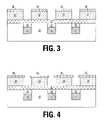
- FIG. 3is a cross-sectional view during the manufacturing process that shows the formation of vias by removing earlier deposited layers, so that the phase change memory cells can be formed in the vias in the word line-shaped n-type material.
- FIG. 4is a cross-sectional view during the manufacturing process that shows undercut etching to affect the subsequent deposition of p-type silicon.
- FIG. 5is a cross-sectional view during the manufacturing process that shows the deposition of p-type silicon, where the p-type silicon is the other doping type of the diode structure.
- FIG. 6is a cross-sectional view during the manufacturing process that shows removal of the p-type silicon to form spacers of p-type material in the vias formed earlier.
- FIG. 7is a cross-sectional view during the manufacturing process that shows the formation, between the p-type spacers, of holes through the silicon oxide layer in which programmable resistive material is to be deposited.
- FIG. 8is a cross-sectional view during the manufacturing process that shows deposition of programmable resistive material.
- FIG. 9is a cross-sectional view during the manufacturing process that shows the removal of excess programmable resistive material.
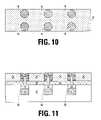
- FIG. 10is a top view, of the same step shown in FIG. 11 , during the manufacturing process that shows oxide deposition to fill in the remaining volume of the vias, and chemical mechanical polishing of excess fill-in oxide.
- FIG. 11is a cross-sectional view, of the same step shown in FIG. 10 , during the manufacturing process that shows oxide deposition to fill in the remaining volume of the vias, and chemical mechanical polishing of excess fill-in oxide.
- FIG. 12is a top view, of the same step shown in FIG. 13 , during the manufacturing process that shows the removal of excess n-type material to leave n-type material in word line shapes to access the memory cells.
- FIG. 13is a cross-sectional view, of the same step shown in FIG. 12 , during the manufacturing process that shows the removal of excess n-type material to leave n-type material in word line shapes to access the memory cells.
- FIG. 14is a top view, of the same step shown in FIG. 15 , during the manufacturing process that shows the formation of word lines by forming salicide, or self-aligned silicide, thereby reducing the resistance of the word line-shaped n-type material to access the memory cells sufficiently for practical word line operation.
- FIG. 15is a cross-sectional view, of the same step shown in FIG. 14 , during the manufacturing process that shows the formation of word lines by forming salicide, or self-aligned silicide, thereby reducing the resistance of the word line-shaped n-type material to access the memory cells sufficiently for practical word line operation.
- FIG. 16is a top view, of the same device shown in FIG. 17 , showing an alternative phase change memory cell with diode structure, to the one shown in FIG. 14 .
- FIG. 17is a cross-sectional view, of the same device shown in FIG. 16 , showing an alternative phase change memory cell with diode structure, to the one shown in FIG. 15 .
- FIG. 18is a cross-sectional view during the manufacturing process that shows the deposition of heater material prior to the deposition of programmable resistive material, thereby reducing the amount of programmable resistive material to undergo heating.
- FIG. 19is a cross-sectional view during the manufacturing process that shows the removal of excess heater material prior to the deposition of programmable resistive material, thereby reducing the amount of programmable resistive material to undergo heating.
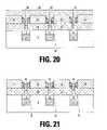
- FIG. 20is a cross-sectional view during the manufacturing process that shows deposition of programmable resistive material.
- FIG. 21is a cross-sectional view during the manufacturing process that shows the removal of excess programmable resistive material.
- FIG. 22is a top view, of the same step shown in FIG. 23 , during the manufacturing process that shows oxide deposition to fill in the remaining volume of the vias, and chemical mechanical polishing of excess fill-in oxide.
- FIG. 23is a cross-sectional view, of the same step shown in FIG. 22 , during the manufacturing process that shows oxide deposition to fill in the remaining volume of the vias, and chemical mechanical polishing of excess fill-in oxide.
- FIG. 24is a top view, of the same step shown in FIG. 25 , during the manufacturing process that shows the removal of excess n-type material to leave n-type material in word line shapes to access the memory cells.
- FIG. 25is a cross-sectional view, of the same step shown in FIG. 24 , during the manufacturing process that shows the removal of excess n-type material to leave n-type material in word line shapes to access the memory cells.
- FIG. 26is a top view during the manufacturing process that shows the formation of word lines by forming conductive word line spacers along the word line-shaped n-type material, thereby reducing the resistance sufficiently for practical word line operation.
- FIG. 27is a block diagram of a nonvolatile memory integrated circuit, with an array of programmable resistive memory cells having a diode structure.
- Various embodimentsare directed at a manufacturing method for memory, such as nonvolatile embedded memory implementing programmable resistance RAM.
- programmable resistance device RAMare resistance memory (RRAM), polymer memory, and phase change memory (PCRAM).
- RRAMresistance memory
- PCRAMphase change memory
- the programmable resistive elementsare formed to have a cross-section small than the cross-section of the upper portion of the interlayer contacts of programmable resistance RAM.
- FIGS. 1-15are a sample process flow to make a programmable resistive device with a diode structure.
- FIG. 1is a cross-sectional view during the manufacturing process that shows the formation of bit lines in an oxide.
- FEOLor front end of line
- processingis performed, to complete early steps in semiconductor fabrication, such as up to but not including first metallization.
- Such early stepsinclude forming the transistor circuitry, multiple semiconductor layers, and interlayer contacts among the multiple semiconductor layers.
- Bit linesare formed in the oxide 10 , such as a bilayer bit line of W 11 and TiN 12 .
- Other example materials for the metal bit linesare TiN/AlCu/Ti/TiN, TaN/Cu.
- the bit linesare in parallel (extending into and out of FIG. 1 ) and collectively define a planar orientation. Also, each bit line by itself defines a linear orientation.
- FIG. 2is a cross-sectional view during the manufacturing process that shows the deposition of n-type silicon layer between silicon oxide layers, where the n-type silicon layer is one doping type of the diode structure.
- Silicon oxide layer 20is deposited.
- Silicon oxide layer 20is a nonconductive layer that isolates the bit lines 11 and 12 from the subsequently formed N-type silicon layer 26 and P-type silicon 39 .
- N-type silicon layer 26is deposited.
- Silicon oxide layer 25is deposited.
- FIG. 3is a cross-sectional view during the manufacturing process that shows the formation of vias by removing earlier deposited layers, so that the phase change memory cells can be formed in the vias in the word line-shaped n-type material.
- the holesare etched (via e.g. reactive ion etching) through the top silicon oxide layer 25 and the n-type silicon layer 26 .
- Wet etching, dry etching, or some combination of wet etching and dry etchingare alternative methods.
- the bottom silicon oxide layer 28acts as an etch stop for removing the vias in the n-type silicon layer 26 . Separate islands are formed of top silicon oxide layer 28 and the n-type silicon layer 27 .
- FIG. 4is a cross-sectional view during the manufacturing process that shows undercut etching to affect the subsequent deposition of p-type silicon.
- An undercutis established between the n-type silicon layer 27 and the top silicon oxide layer 28 , by purposely overetching the n-type silicon layer 27 .
- the remaining portionis n-type silicon layer 29 .
- FIG. 5is a cross-sectional view during the manufacturing process that shows the deposition of p-type silicon, where the p-type silicon is the other doping type of the diode structure.
- P-type silicon 39is deposited to fill the vias between the islands of top silicon oxide layer 28 and the n-type silicon layer 27 . However, the filling is incomplete, leaving empty pockets within the p-type silicon 39 . One empty pocket of p-type silicon 39 is in each via.
- FIG. 6is a cross-sectional view during the manufacturing process that shows removal of the p-type silicon to form spacers of p-type material in the vias formed earlier.
- the p-type silicon spacers 40remain after the etching.
- the p-type silicon spacers 40have an annular shape with an exterior surface in contact with the n-type silicon layer 29 , defining a junction area, and providing a diode junction.
- the purpose of the undercut between the n-type silicon layer 27 and the top silicon oxide layer 28has been fulfilled by the formation of the p-type silicon spacers 40 .
- the remaining cavity in the vias between the p-type silicon spacers 40is to be filled by programmable resistive elements, and its size is determined by the size of the undercut formed in FIG. 4 .
- the size of the undercutis more controllable than the size of the vias formed in FIG. 3 .
- the size variation of the p-type silicon spacers 40(which act as diode first terminals) is greater across a sample quantity of memory cells on an array, than the size variation of the programmable resistive elements across the same sample quantity of memory cells on the same array.
- FIG. 7is a cross-sectional view during the manufacturing process that shows the formation, between the p-type spacers, of holes through the silicon oxide layer in which programmable resistive material is to be deposited.
- the top silicon oxide layer 28 of the islandis removed.
- the bottom silicon oxide layer 20 that is exposed by the p-type silicon spacers 40is removed, leaving space for the programmable resistive material to be deposited.
- FIG. 8is a cross-sectional view during the manufacturing process that shows deposition of programmable resistive material.
- Programmable resistive material 59is deposited, filling the holes in the bottom silicon oxide layer 20 , and filling the space between the p-type silicon spacers 40 .
- Embodiments of the memory cellinclude phase change based memory materials, including chalcogenide based materials and other materials, for the resistive elements 52 and 54 .
- Chalcogensinclude any of the four elements oxygen (O), sulfur (S), selenium (Se), and tellurium (Te), forming part of group VI of the periodic table.
- Chalcogenidescomprise compounds of a chalcogen with a more electropositive element or radical.
- Chalcogenide alloyscomprise combinations of chalcogenides with other materials such as transition metals.
- a chalcogenide alloyusually contains one or more elements from column six of the periodic table of elements, such as germanium (Ge) and tin (Sn).
- chalcogenide alloysinclude combinations including one or more of antimony (Sb), gallium (Ga), indium (In), and silver (Ag).
- Sbantimony
- Gagallium
- Inindium
- silversilver
- phase change based memory materialsinclude alloys of: Ga/Sb, In/Sb, In/Se, Sb/Te, Ge/Te, Ge/Sb/Te, In/Sb/Te, Ga/Se/Te, Sn/Sb/Te, In/Sb/Ge, Ag/In/Sb/Te, Ge/Sn/Sb/Te, Ge/Sb/Se/Te and Te/Ge/Sb/S.
- compositionscan be workable.
- the compositionscan be characterized as Te a Ge b Sb 100 ⁇ (a+b) .
- One researcherhas described the most useful alloys as having an average concentration of Te in the deposited materials well below 70%, typically below about 60% and ranged in general from as low as about 23% up to about 58% Te and most preferably about 48% to 58% Te.
- Concentrations of Gewere above about 5% and ranged from a low of about 8% to about 30% average in the material, remaining generally below 50%. Most preferably, concentrations of Ge ranged from about 8% to about 40%. The remainder of the principal constituent elements in this composition was Sb.
- a transition metalsuch as chromium (Cr), iron (Fe), nickel (Ni), niobium (Nb), palladium (Pd), platinum (Pt) and mixtures or alloys thereof may be combined with Ge/Sb/Te to form a phase change alloy that has programmable resistive properties.
- chromium (Cr)iron (Fe), nickel (Ni), niobium (Nb), palladium (Pd), platinum (Pt) and mixtures or alloys thereof
- Ge/Sb/Techromium
- Specific examples of memory materials that may be usefulare given in Ovshinsky '112 at columns 11-13, which examples are hereby incorporated by reference.
- Chalcogenides and other phase change materialsare doped with impurities in some embodiments to modify conductivity, transition temperature, melting temperature, and other properties of memory elements using the doped chalcogenides.
- Representative impurities used for doping chalcogenidesinclude nitrogen, silicon, oxygen, silicon dioxide, silicon nitride, copper, silver, gold, aluminum, aluminum oxide, tantalum, tantalum oxide, tantalum nitride, titanium and titanium oxide. See, e.g. U.S. Pat. No. 6,800,504, and U.S. Patent Application Publication No. US 2005/0029502.
- Phase change alloysare capable of being switched between a first structural state in which the material is in a generally amorphous solid phase, and a second structural state in which the material is in a generally crystalline solid phase in its local order in the active channel region of the cell. These alloys are at least bistable.
- amorphousis used to refer to a relatively less ordered structure, more disordered than a single crystal, which has the detectable characteristics such as higher electrical resistivity than the crystalline phase.
- crystallineis used to refer to a relatively more ordered structure, more ordered than in an amorphous structure, which has detectable characteristics such as lower electrical resistivity than the amorphous phase.
- phase change materialsmay be electrically switched between different detectable states of local order across the spectrum between completely amorphous and completely crystalline states.
- Other material characteristics affected by the change between amorphous and crystalline phasesinclude atomic order, free electron density and activation energy.
- the materialmay be switched either into different solid phases or into mixtures of two or more solid phases, providing a gray scale between completely amorphous and completely crystalline states.
- the electrical properties in the materialmay vary accordingly.
- Phase change alloyscan be changed from one phase state to another by application of electrical pulses. It has been observed that a shorter, higher amplitude pulse tends to change the phase change material to a generally amorphous state. A longer, lower amplitude pulse tends to change the phase change material to a generally crystalline state. The energy in a shorter, higher amplitude pulse is high enough to allow for bonds of the crystalline structure to be broken and short enough to prevent the atoms from realigning into a crystalline state. Appropriate profiles for pulses can be determined, without undue experimentation, specifically adapted to a particular phase change alloy. In following sections of the disclosure, the phase change material is referred to as GST, and it will be understood that other types of phase change materials can be used. A material useful for implementation of a PCRAM described herein is Ge 2 Sb 2 Te 5 .
- programmable resistive memory materialsmay be used in other embodiments of the invention, including N2 doped GST, Ge x Sb y , or other material that uses different crystal phase changes to determine resistance; Pr x Ca y MnO 3 , Pr x Sr y MnO 3 , ZrO x , or other material that uses an electrical pulse to change the resistance state; 7,7,8,8-tetracyanoquinodimethane (TCNQ), methanofullerene 6,6-phenyl C61-butyric acid methyl ester (PCBM), TCNQ-PCBM, Cu-TCNQ, Ag-TCNQ, C 60 -TCNQ, TCNQ doped with other metal, or any other polymer material that has bistable or multi-stable resistance state controlled by an electrical pulse.
- TCNQ7,7,8,8-tetracyanoquinodimethane
- PCBMmethanofullerene 6,6-phenyl C61-butyric acid methyl ester
- GeSbTe with doping, such as N—, Si—, Ti—, or other element dopingis alternatively used.
- An exemplary method for forming chalcogenide materialuses PVD-sputtering or magnetron-sputtering method with source gas(es) of Ar, N 2 , and/or He, etc. at the pressure of 1 mTorr ⁇ 100 mTorr.
- the depositionis usually done at room temperature.
- a collimater with an aspect ratio of 1 ⁇ 5can be used to improve the fill-in performance.
- a DC bias of several tens of volts to several hundreds of voltsis also used.
- the combination of DC bias and the collimatercan be used simultaneously.
- a post-deposition annealing treatment in vacuum or in an N 2 ambientis optionally performed to improve the crystallize state of chalcogenide material.
- the annealing temperaturetypically ranges from 100° C. to 400° C. with an anneal time of less than 30 minutes.
- chalcogenide materialdepends on the design of cell structure.
- a chalcogenide material with thickness of higher than 8 nmcan have a phase change characterization so that the material exhibits at least two stable resistance states.
- CMR material that includes Mn oxideis alternatively used.
- An exemplary method for forming CMR materialuses PVD sputtering or magnetron-sputtering method with source gases of Ar, N 2 , O 2 , and/or He, etc. at the pressure of 1 mTorr ⁇ 100 mTorr.
- the deposition temperaturecan range from room temperature to ⁇ 600° C., depending on the post deposition treatment condition.
- a collimater with an aspect ratio of 1 ⁇ 5can be used to improve the fill-in performance.
- the DC bias of several tens of volts to several hundreds of voltsis also used.
- the combination of DC bias and the collimatercan be used simultaneously.
- a magnetic field of several tens of Gauss to as much as a Tesla (10,000 Gauss)may be applied to improve the magnetic crystallized phase.
- a post-deposition annealing treatment in vacuum or in an N2 ambient or O2/N2 mixed ambientis optionally used to improve the crystallized state of CMR material.
- the annealing temperaturetypically ranges from 400° C. to 600° C. with an anneal time of less than 2 hours.
- the thickness of CMR materialdepends on the design of the cell structure.
- the CMR thickness of 10 nm to 200 nmcan be used for the core material.
- a buffer layer of YBCO(YBaCuO 3 , which is a type of high temperature superconductor material) is often used to improve the crystallized state of CMR material.
- the YBCOis deposited before the deposition of CMR material.
- the thickness of YBCOranges from 30 nm to 200 nm.
- An exemplary formation methoduses a PVD sputtering or magnetron-sputtering method with reactive gases of Ar, N 2 , O 2 , and/or He, etc.
- a collimater with an aspect ratio of 1 ⁇ 5can be used to improve the fill-in performance.
- the DC bias of several tens of volts to several hundreds of voltsis also used. If desired, the combination of DC bias and the collimater can be used simultaneously.
- a post-deposition annealing treatment in vacuum or in an N 2 ambient or O 2 /N 2 mixed ambientis optionally performed to improve the oxygen distribution of metal oxide.
- the annealing temperatureranges from 400° C. to 600° C. with an anneal time of less than 2 hours.
- An alternative formation methoduses a PVD sputtering or magnetron-sputtering method with reactive gases of Ar/O 2 , Ar/N 2 /O 2 , pure O 2 , He/O 2 , He/N 2 /O 2 etc. at the pressure of 1 mTorr ⁇ 100 mTorr, using a target of metal oxide, such as Ni, Ti, Al, W, Zn, Zr, or Cu etc.
- the depositionis usually done at room temperature.
- a collimater with an aspect ratio of 1 ⁇ 5can be used to improve the fill-in performance.
- a DC bias of several tens of volts to several hundreds of voltsis also used. If desired, the combination of DC bias and the collimater can be used simultaneously.
- a post-deposition annealing treatment in vacuum or in an N 2 ambient or O 2 /N 2 mixed ambientis optionally performed to improve the oxygen distribution of metal oxide.
- the annealing temperatureranges from 400° C. to 600° C. with an anneal time of less than 2 hours.
- Yet another formation methoduses oxidation by a high temperature oxidation system, such as a furnace or a rapid thermal pulse (“RTP”) system.
- the temperatureranges from 200° C. to 700° C. with pure O 2 or N 2 /O 2 mixed gas at a pressure of several mTorr to 1 atm. The time can range several minute to hours.
- Another oxidation methodis plasma oxidation.
- An RF or a DC source plasma with pure O 2 or Ar/O 2 mixed gas or Ar/N 2 /O 2 mixed gas at a pressure of 1 mTorr to 100 mTorris used to oxidize the surface of metal, such as Ni, Ti, Al, W, Zn, Zr, or Cu etc.
- the oxidation timeranges several seconds to several minutes.
- the oxidation temperatureranges from room temperature to 300° C., depending on the degree of plasma oxidation.
- a fourth type of memory materialis a polymer material, such as TCNQ with doping of Cu, C 60 , Ag etc. or PCBM-TCNQ mixed polymer.
- TCNQpolymer material
- One formation methoduses evaporation by thermal evaporation, e-beam evaporation, or molecular beam epitaxy (“MBE”) system.
- MBEmolecular beam epitaxy
- a solid-state TCNQ and dopant pelletsare co-evaporated in a single chamber.
- the solid-state TCNQ and dopant pelletsare put in a W-boat or a Ta-boat or a ceramic boat.
- a high electrical current or an electron-beamis applied to melt the source so that the materials are mixed and deposited on wafers. There are no reactive chemistries or gases.
- the depositionis done at a pressure of 10 ⁇ 4 Torr to 10 ⁇ 10 Torr.
- the wafer temperatureranges from room temperature to 200° C.
- a post-deposition annealing treatment in vacuum or in an N 2 ambientis optionally performed to improve the composition distribution of polymer material.
- the annealing temperatureranges from room temperature to 300° C. with an anneal time of less than 1 hour.
- Another technique for forming a layer of polymer-based memory materialis to use a spin-coater with doped-TCNQ solution at a rotation of less than 1000 rpm. After spin-coating, the wafer held (typically at room temperature or temperature less than 200° C.) for a time sufficient for solid-state formation. The hold time ranges from several minutes to days, depending on the temperature and on the formation conditions.
- FIG. 9is a cross-sectional view during the manufacturing process that shows the removal of excess programmable resistive material.
- Excess programmable resistive material 59is etched back, leaving the programmable resistive material 60 in the gaps in the bottom silicon oxide layer 20 , and partly in the space between the p-type silicon spacers 40 .
- the programmable resistive material 60has a sidewall surface connected to the interior surface of the p-type silicon spacers 40 , and a bottom surface conductively coupled to the bit lines 11 and 12 .
- the programmable resistive material 60is physically separated from the n-type silicon layer 29 by p-type silicon spacers 40 .
- FIG. 10is a top view, of the same step shown in FIG. 11 , during the manufacturing process that shows oxide deposition to fill in the remaining volume of the vias, and chemical mechanical polishing of excess fill-in oxide.
- Oxideis formed to fill the remaining spaces between the p-type silicon spacers 40 , and the remaining spaces between the n-type silicon 29 . Excess oxide over the n-type silicon 29 is removed by chemical mechanical polishing.
- Oxide 70remains, filling spaces between the p-type silicon spacers 40 , and the spaces between the n-type silicon 29 .
- the oxideresults in the top surface of the programmable resistive material 60 not being used as a surface through which current passes. However, the relative smaller size of the top surface compared to the sidewall surface of the programmable resistive material 60 is illustrative of a greater current capacity.
- FIG. 11is a cross-sectional view, of the same step shown in FIG. 10 , during the manufacturing process that shows oxide deposition to fill in the remaining volume of the vias, and chemical mechanical polishing of excess fill-in oxide.
- FIG. 12is a top view, of the same step shown in FIG. 13 , during the manufacturing process that shows the lithographic definition and removal (via e.g. reactive ion etching) of excess n-type material to leave n-type material in word line shapes to access the memory cells. Excess n-type silicon material 29 is removed, leaving word line-shaped n-type silicon material 30 . Although covered by other layers, bit lines 11 are shown to illustrate both directions of accessing the memory cells.
- FIG. 13is a cross-sectional view, of the same step shown in FIG. 12 , during the manufacturing process that shows the removal of excess n-type material to leave n-type material in word line shapes to access the memory cells.
- FIG. 14is a top view, of the same step shown in FIG. 15 , during the manufacturing process that shows the formation of word lines by forming salicide, or self-aligned silicide, thereby reducing the resistance of the word line-shaped n-type material to access the memory cells sufficiently for practical word line operation.
- Salicide 90is formed on word line-shaped n-type silicon material 30 .
- the word linesare in parallel and collectively define a planar orientation. Also, each word line by itself defines a linear orientation. This planar orientation is parallel with the planar orientation defined by the bit lines. Both planar orientations are orthogonal to the diode junction orientation.
- FIG. 15is a cross-sectional view, of the same step shown in FIG. 14 , during the manufacturing process that shows the formation of word lines by forming salicide, or self-aligned silicide, thereby reducing the resistance of the word line-shaped n-type material to access the memory cells sufficiently for practical word line operation.
- a driving currentflows through: at least one of the conductive columns 11 / 12 conductively coupled to a programmable resistive element 60 , the programmable resistive element 60 conductively connected to the particular one of the diode structures, the particular one of the diode structures (each including word line-shaped n-type silicon material 30 and a p-type silicon spacer 40 ), and then at least one of the conductive rows 90 conductively coupled to the particular one of the diode structures.
- the current pathis reversed.
- FIG. 16is a top view, of the same device shown in FIG. 17 , showing an alternative phase change memory cell with diode structure, to the one shown in FIG. 14 .
- Word line 30 and bit line 11access the memory cell.
- Word line 30includes one doping type (e.g., n-type or p-type) of a diode structure.
- Semiconductor 40has another doping type (e.g., p-type or n-type) of the diode structure. Together, word line 30 and semiconductor 40 form a diode structure.
- the data of the nonvolatile memory cellis stored by the phase change material 60 .
- FIG. 17is a cross-sectional view, of the same device shown in FIG. 16 , showing an alternative phase change memory cell with diode structure, to the one shown in FIG. 15 .
- Active volume 62is the portion of the phase change material 60 which actually changes characteristics to store the data of the nonvolatile memory cell.
- the memory cellis accessed by bilayer bit line of W 11 and TiN 12 .
- Silicon oxide 20is nonconductive and isolates the bit lines 11 and 12 from the subsequently formed N-type silicon layer 26 and P-type silicon 39 .
- FIGS. 1-7 and 18 - 26are another sample process flow to make a programmable resistive device with a diode structure.
- each of the nonvolatile memory cellshas a size of no more than 5 F ⁇ 2.
- Fis a minimum feature size of a lithographic process used in manufacture of the integrated circuit.
- FIG. 18is a cross-sectional view during the manufacturing process that shows the deposition of heater material prior to the deposition of programmable resistive material, thereby reducing the amount of programmable resistive material to undergo heating.
- Excess heater material TiN 49is deposited by chemical vapor deposition, filling at least the holes in the bottom silicon oxide layer 20 .
- FIG. 19is a cross-sectional view during the manufacturing process that shows the removal of excess heater material prior to the deposition of programmable resistive material, thereby reducing the amount of programmable resistive material to undergo heating.
- Excess heater material TiN 49is etched back, such as part of the material in the holes in the bottom silicon oxide layer 20 , any material filling the space between the p-type silicon spacers 40 , and any other excess material in the vias between n-type silicon 29 or covering the n-type silicon 29 .
- the remaining heater material TiN 50partly fills the holes in the bottom silicon oxide layer 20 .
- FIG. 20is a cross-sectional view during the manufacturing process that shows deposition of programmable resistive material.
- Programmable resistive material 59is deposited, filling the holes in the bottom silicon oxide layer 20 , and filling the space between the p-type silicon spacers 40 .
- FIG. 21is a cross-sectional view during the manufacturing process that shows the removal of excess programmable resistive material.
- Excess programmable resistive material 59is etched back, leaving the programmable resistive material 60 in the gaps in the bottom silicon oxide layer 20 , and partly in the space between the p-type silicon spacers 40 .
- the programmable resistive material 60has a sidewall surface connected to the interior surface of the p-type silicon spacers 40 , and a bottom surface conductively coupled to the bit lines 11 and 12 .
- the programmable resistive material 60is physically separated from the n-type silicon layer 29 by p-type silicon spacers 40 .
- FIG. 22is a top view, of the same step shown in FIG. 23 , during the manufacturing process that shows oxide deposition to fill in the remaining volume of the vias, and chemical mechanical polishing of excess fill-in oxide.
- Oxideis formed to fill the remaining spaces between the p-type silicon spacers 40 , and the remaining spaces between the n-type silicon 29 . Excess oxide over the n-type silicon 29 is removed by chemical mechanical polishing.
- Oxide 70remains, filling spaces between the p-type silicon spacers 40 , and the spaces between the n-type silicon 29 .
- the oxideresults in the top surface of the programmable resistive material 60 not being used as a surface through which current passes. However, the relative smaller size of the top surface compared to the sidewall surface of the programmable resistive material 60 is illustrative of a greater current capacity.
- FIG. 23is a cross-sectional view, of the same step shown in FIG. 22 , during the manufacturing process that shows oxide deposition to fill in the remaining volume of the vias, and chemical mechanical polishing of excess fill-in oxide.
- FIG. 24is a top view, of the same step shown in FIG. 25 , during the manufacturing process that shows the lithographic definition and removal (via e.g. reactive ion etching) of excess n-type material to leave n-type material in word line shapes to access the memory cells. Excess n-type silicon material 29 is removed, leaving word line-shaped n-type silicon material 30 . Although covered by other layers, bit lines 11 are shown to illustrate both directions of accessing the memory cells.
- FIG. 25is a cross-sectional view, of the same step shown in FIG. 24 , during the manufacturing process that shows the removal of excess n-type material to leave n-type material in word line shapes to access the memory cells.
- FIG. 26is a top view during the manufacturing process that shows the formation of word lines by forming conductive word line spacers along the word line-shaped n-type material, thereby reducing the resistance sufficiently for practical word line operation.
- Word line metal TiN 80is formed alongside the word line-shaped n-type silicon 30 , substantially reducing the resistance of the word line structure.
- the word linesare in parallel and collectively define a planar orientation. Also, each word line by itself defines a linear orientation. This planar orientation is parallel with the planar orientation defined by the bit lines. Both planar orientations are orthogonal to the diode junction orientation.
- a driving currentflows through: at least one of the conductive columns 11 / 12 conductively coupled to a programmable resistive element 60 , the programmable resistive element 60 conductively connected to the particular one of the diode structures, the particular one of the diode structures (each including word line-shaped n-type silicon material 30 and a p-type silicon spacer 40 ), and then at least one of the conductive rows 80 conductively coupled to the particular one of the diode structures.
- the current pathis reversed.
- FIG. 27is a block diagram of a nonvolatile memory integrated circuit, with an array of programmable resistive memory cells having a diode structure.
- the integrated circuit 150includes a memory array 100 implemented using memory cells with resistive elements on a semiconductor substrate.
- the programmable resistive cellsare separated by semiconductor diode structures as described herein.
- a sample quantity of memory cells of the array 100(such as on different sides of the array 100 ) has a size variation of the programmable resistive elements 60 less than a size variation of the diode first terminals 40 , because of the highly controllable programmable resistive element sizes, as discussed in connection with FIG. 6 .
- Addressesare supplied on bus 105 to column decoder 103 and row decoder 101 .
- Sense amplifiers and data-in structures in block 106are coupled to the column decoder 103 via data bus 107 .
- Datais supplied via the data-in line 111 from input/output ports on the integrated circuit 150 , or from other data sources internal or external to the integrated circuit 150 , to the data-in structures in block 106 .
- Datais supplied via the data-out line 115 from the block 106 to input/output ports on the integrated circuit 150 , or to other data destinations internal or external to the integrated circuit 150 .
- the integrated circuit 150may also include circuitry directed a mission function other than the nonvolatile storage with resistive elements (not shown). Bias arrangement state machine 109 controls the application of bias arrangement supply voltages.
- bit lines and word linescorrespond to the bit lines 104 leading to the column decoder 103 and to the word lines 102 leading to the row decoder 101 .
- the memory array 100include millions of cells covers a relatively large area on a device, over which the lithographically formed vias will vary in size over a range ⁇ V, where V represents the nominal size of the via. Therefore, if one samples a first memory cell in a first sector of the array, and compares that cell with a second memory cell in a second sector of the array, it is likely that the via used for formation of the memory element will differ by as much as ⁇ V.
- the width of the surface of the bottom electrode in contact with the memory elementin embodiments of the present invention will vary by at most 2 ⁇ O, where O represents the nominal size of the overhang characterizing the undercut process of FIG. 4 .
- the first cellmay have a width of dimension V of about 92 nm and a dimension CD of about 39 nm, while the second cell may have a width of dimension V of about 88 nm, and a dimension CD of about 41 nm.
- a structureresults in which the width of the memory element in the first cell as measured varies from width of the memory element in the second cell by 4/92, or 4.3% of the width V, in the example illustrated.
- the width of the critical dimension in the first cellvaries from that in the second cell by 2/92, or 2.2% of the width V. Therefore the critical dimensions of the sampled memory cells vary by less than the variations in the width of the memory elements in a way not possible in the prior art.
- a layer“covers” another layer or is “above” another layer, even in the presence of a layer (e.g., between the covering layer and the covered layer, or between the “above” layer and the “below” layer.
- a layeris “between” two other layers, regardless of any layers on either side.
Landscapes
- Engineering & Computer Science (AREA)
- Manufacturing & Machinery (AREA)
- Chemical & Material Sciences (AREA)
- Materials Engineering (AREA)
- Semiconductor Memories (AREA)
Abstract
Description
- International Business Machines Corporation, a New York corporation; Macronix International Corporation, Ltd., a Taiwan corporation; and Qimonda, are parties to a Joint Research Agreement.
- 1. Field of the Invention
- The invention relates to integrated circuit nonvolatile memory. In particular, the invention relates to programmable resistive nonvolatile memory, such as phase change memory.
- 2. Description of Related Art
- Nonvolatile memory stores data without requiring a continuous supply of power. Programmable resistive memory such as phase change memory is an example of nonvolatile memory. A high current reset electrical pulse melts and quenches the programmable resistive element into an amorphous state, raising the resistance of the programmable resistive element. A low current set electrical pulse crystallizes and lowers the resistance of the programmable resistive element.
- Although the reset electrical pulse requires a high current, the structure of a programmable resistive RAM cell is a factor limiting the amount of current flowing through the programmable resistive element of the cell. The physical positioning of the contacts on either end of the programmable resistive element, requires the high current reset pulse to flow through an end of the programmable resistive element with a relatively small physical cross-section. Accordingly, it would be desirable if the high current reset pulse could flow through a larger physical area to reach the programmable resistive RAM cell.
- One aspect of the technology is an integrated circuit with nonvolatile memory cells, so that diode structures are formed adjacent to the programmable resistive elements of the nonvolatile memory cells. The circuit includes conductive columns, conductive rows, a nonconductive layer separating the conductive columns from the diode structures, the diode structures, and the programmable restive elements.
- The conductive rows and columns are conductively coupled to the nonvolatile memory cells. They correspond typically to bit lines and word lines.
- In some embodiments, the conductive rows are typically arranged in parallel, as are the conductive columns. The conductive rows and columns each define a planar orientation, parallel with each other.
- The diode structures connect the programmable resistive elements with the conductive rows. Each of the diode structures includes a first terminal and a second terminal.
- In some embodiments, the first terminal of each diode structure has an exterior surface, and an interior surface connected to at least one of the programmable resistive elements. In some embodiments, the second terminal of each diode structure is in contact with a junction area on the exterior surface of the first terminal providing a diode junction oriented orthogonal to the planar orientations of the conductive rows and columns.
- In some embodiments, the first terminal of each diode structure has an annular shape with an exterior surface, and an interior surface surrounding at least one of the programmable resistive elements. In some embodiments, the second terminal of each diode structure is in contact with the exterior surface of the first terminal.
- In some embodiments, the first terminals physically separate the programmable resistive elements and the second terminals.
- In some embodiments, the programmable resistive elements each have a sidewall surface connected to the interior surface of the first terminal of at least one of the diode structures, and a bottom surface conductively coupled to at least one of the conductive columns.
- The programmable resistive elements each have a sidewall surface surrounded by the interior surface of the first terminal of at least one of the diode structures, and a bottom surface conductively coupled to at least one of the conductive columns.
- In some embodiments, the programmable resistive elements each have a top surface having a smaller area than the sidewall surface. In some embodiments, the programmable resistive elements include at least a chalcogenide.
- In some embodiments of the diode structures, a self-aligned silicide is formed over the second terminals to form the second terminals. In some embodiments the conductive rows are formed along the diode structures, such as with conductive spacers adjacent to the second terminals of the diode structures. In various embodiments, the bit lines and word lines correspond to the self-aligned silicide or the conductive spacers, or if material corresponding to the self-aligned silicide or the conductive spacers is absent, then to conductive traces that connect the circuit to the remaining circuitry.
- In some embodiments, the second terminal and the first terminal are arranged, so that in response to a forward bias on a particular one of the diode structures, a driving current flows through: at least one of the conductive rows conductively coupled to the particular one of the diode structures, the particular one of the diode structures, a programmable resistive element of the programmable resistive elements conductively connected to the particular one of the diode structures, and at least one of the conductive columns conductively coupled to the programmable resistive element. In many embodiments, the first and second terminals of the diode structures have opposite doping types.
- The highly controllable process is an advantage of several embodiments. In some embodiments, each nonvolatile memory cell formed by the method has a size of no more than 5 F̂2, whereby F is a minimum feature size of a lithographic process used in manufacture of the method. In some embodiments, the diode structures include a sample quantity of diode structures. The first terminals of the sample quantity have a size variation of at least about 4 nm. The programmable resistive elements of the sample quantity have a second size variation of less than about 2 nm, demonstrating the process control over the programmable resistive elements despite a lack of corresponding process control over the first terminals. More generally, in another embodiment, the size variation of the programmable resistive elements of the sample quantity is less than the size variation of the first terminals of the sample quantity. An exemplary choice of the sample quantity of diode structures includes diode structures on different sides of the array of nonvolatile memory cells.
- Another aspect of the technology is a method of forming the integrated circuit as described.
- In many embodiments, the first terminals are formed after the second terminals. In some embodiments, the second terminals are formed as follows. A layer of the second terminals is formed over the conductive columns, and cavities are formed in the layer of the second terminals by removing material from the layer of the second terminals. Later steps such as forming the first terminals and forming the programmable resistive elements occur at least partly in the cavities of the layer of the second terminals. A further embodiment adds the following, before the first terminals are formed. After the layer of the second terminals is formed, an oxide layer is formed over the layer of the second terminals; and an undercut is formed in the cavities of the layer of the second terminals and the oxide layer, by laterally removing more material from the layer of the second terminals than from the oxide layer. In an embodiment this undercut determines the sizes of the programmable resistive elements.
- In many embodiments, the first terminals are formed as follows. A layer of the first terminals is formed over the second terminals. In some embodiments at least part of the layer of the first terminals positioned outside the cavities of the second terminals is removed. In some embodiments the layer of the first terminals at least partly fills cavities of the second terminals. In some embodiments, after the conductive columns are formed, an oxide layer covering the conductive columns is formed, and optionally part of the layer of the first terminals and part of the oxide layer are removed to leave cavities in which to form programmable resistive elements.
- Other aspect of the technology is an integrated circuit with multiple nonvolatile memory cells, or one nonvolatile memory cell, as disclosed herein.
- Other embodiments are disclosed herein.
FIG. 1 is a cross-sectional view during the manufacturing process that shows the formation of bit lines in an oxide.FIG. 2 is a cross-sectional view during the manufacturing process that shows the deposition of n-type silicon layer between silicon oxide layers, where the n-type silicon layer is one doping type of the diode structure.FIG. 3 is a cross-sectional view during the manufacturing process that shows the formation of vias by removing earlier deposited layers, so that the phase change memory cells can be formed in the vias in the word line-shaped n-type material.FIG. 4 is a cross-sectional view during the manufacturing process that shows undercut etching to affect the subsequent deposition of p-type silicon.FIG. 5 is a cross-sectional view during the manufacturing process that shows the deposition of p-type silicon, where the p-type silicon is the other doping type of the diode structure.FIG. 6 is a cross-sectional view during the manufacturing process that shows removal of the p-type silicon to form spacers of p-type material in the vias formed earlier.FIG. 7 is a cross-sectional view during the manufacturing process that shows the formation, between the p-type spacers, of holes through the silicon oxide layer in which programmable resistive material is to be deposited.FIG. 8 is a cross-sectional view during the manufacturing process that shows deposition of programmable resistive material.FIG. 9 is a cross-sectional view during the manufacturing process that shows the removal of excess programmable resistive material.FIG. 10 is a top view, of the same step shown inFIG. 11 , during the manufacturing process that shows oxide deposition to fill in the remaining volume of the vias, and chemical mechanical polishing of excess fill-in oxide.FIG. 11 is a cross-sectional view, of the same step shown inFIG. 10 , during the manufacturing process that shows oxide deposition to fill in the remaining volume of the vias, and chemical mechanical polishing of excess fill-in oxide.FIG. 12 is a top view, of the same step shown inFIG. 13 , during the manufacturing process that shows the removal of excess n-type material to leave n-type material in word line shapes to access the memory cells.FIG. 13 is a cross-sectional view, of the same step shown inFIG. 12 , during the manufacturing process that shows the removal of excess n-type material to leave n-type material in word line shapes to access the memory cells.FIG. 14 is a top view, of the same step shown inFIG. 15 , during the manufacturing process that shows the formation of word lines by forming salicide, or self-aligned silicide, thereby reducing the resistance of the word line-shaped n-type material to access the memory cells sufficiently for practical word line operation.FIG. 15 is a cross-sectional view, of the same step shown inFIG. 14 , during the manufacturing process that shows the formation of word lines by forming salicide, or self-aligned silicide, thereby reducing the resistance of the word line-shaped n-type material to access the memory cells sufficiently for practical word line operation.FIG. 16 is a top view, of the same device shown inFIG. 17 , showing an alternative phase change memory cell with diode structure, to the one shown inFIG. 14 .FIG. 17 is a cross-sectional view, of the same device shown inFIG. 16 , showing an alternative phase change memory cell with diode structure, to the one shown inFIG. 15 .FIG. 18 is a cross-sectional view during the manufacturing process that shows the deposition of heater material prior to the deposition of programmable resistive material, thereby reducing the amount of programmable resistive material to undergo heating.FIG. 19 is a cross-sectional view during the manufacturing process that shows the removal of excess heater material prior to the deposition of programmable resistive material, thereby reducing the amount of programmable resistive material to undergo heating.FIG. 20 is a cross-sectional view during the manufacturing process that shows deposition of programmable resistive material.FIG. 21 is a cross-sectional view during the manufacturing process that shows the removal of excess programmable resistive material.FIG. 22 is a top view, of the same step shown inFIG. 23 , during the manufacturing process that shows oxide deposition to fill in the remaining volume of the vias, and chemical mechanical polishing of excess fill-in oxide.FIG. 23 is a cross-sectional view, of the same step shown inFIG. 22 , during the manufacturing process that shows oxide deposition to fill in the remaining volume of the vias, and chemical mechanical polishing of excess fill-in oxide.FIG. 24 is a top view, of the same step shown inFIG. 25 , during the manufacturing process that shows the removal of excess n-type material to leave n-type material in word line shapes to access the memory cells.FIG. 25 is a cross-sectional view, of the same step shown inFIG. 24 , during the manufacturing process that shows the removal of excess n-type material to leave n-type material in word line shapes to access the memory cells.FIG. 26 is a top view during the manufacturing process that shows the formation of word lines by forming conductive word line spacers along the word line-shaped n-type material, thereby reducing the resistance sufficiently for practical word line operation.FIG. 27 is a block diagram of a nonvolatile memory integrated circuit, with an array of programmable resistive memory cells having a diode structure.- Various embodiments are directed at a manufacturing method for memory, such as nonvolatile embedded memory implementing programmable resistance RAM. Examples of programmable resistance device RAM are resistance memory (RRAM), polymer memory, and phase change memory (PCRAM). The programmable resistive elements are formed to have a cross-section small than the cross-section of the upper portion of the interlayer contacts of programmable resistance RAM.
FIGS. 1-15 are a sample process flow to make a programmable resistive device with a diode structure.FIG. 1 is a cross-sectional view during the manufacturing process that shows the formation of bit lines in an oxide. Prior to this, FEOL, or front end of line, processing is performed, to complete early steps in semiconductor fabrication, such as up to but not including first metallization. Such early steps include forming the transistor circuitry, multiple semiconductor layers, and interlayer contacts among the multiple semiconductor layers. Bit lines are formed in theoxide 10, such as a bilayer bit line ofW 11 andTiN 12. Other example materials for the metal bit lines are TiN/AlCu/Ti/TiN, TaN/Cu. The bit lines are in parallel (extending into and out ofFIG. 1 ) and collectively define a planar orientation. Also, each bit line by itself defines a linear orientation.FIG. 2 is a cross-sectional view during the manufacturing process that shows the deposition of n-type silicon layer between silicon oxide layers, where the n-type silicon layer is one doping type of the diode structure.Silicon oxide layer 20 is deposited.Silicon oxide layer 20 is a nonconductive layer that isolates the bit lines11 and12 from the subsequently formed N-type silicon layer 26 and P-type silicon39. Then, N-type silicon layer 26 is deposited.Silicon oxide layer 25 is deposited.FIG. 3 is a cross-sectional view during the manufacturing process that shows the formation of vias by removing earlier deposited layers, so that the phase change memory cells can be formed in the vias in the word line-shaped n-type material. After defining the holes lithographically, the holes are etched (via e.g. reactive ion etching) through the topsilicon oxide layer 25 and the n-type silicon layer 26. Wet etching, dry etching, or some combination of wet etching and dry etching, are alternative methods. The bottomsilicon oxide layer 28 acts as an etch stop for removing the vias in the n-type silicon layer 26. Separate islands are formed of topsilicon oxide layer 28 and the n-type silicon layer 27.FIG. 4 is a cross-sectional view during the manufacturing process that shows undercut etching to affect the subsequent deposition of p-type silicon. An undercut is established between the n-type silicon layer 27 and the topsilicon oxide layer 28, by purposely overetching the n-type silicon layer 27. The remaining portion is n-type silicon layer 29.FIG. 5 is a cross-sectional view during the manufacturing process that shows the deposition of p-type silicon, where the p-type silicon is the other doping type of the diode structure. P-type silicon39 is deposited to fill the vias between the islands of topsilicon oxide layer 28 and the n-type silicon layer 27. However, the filling is incomplete, leaving empty pockets within the p-type silicon39. One empty pocket of p-type silicon39 is in each via.FIG. 6 is a cross-sectional view during the manufacturing process that shows removal of the p-type silicon to form spacers of p-type material in the vias formed earlier. The p-type silicon spacers 40 remain after the etching. The p-type silicon spacers 40 have an annular shape with an exterior surface in contact with the n-type silicon layer 29, defining a junction area, and providing a diode junction. The purpose of the undercut between the n-type silicon layer 27 and the topsilicon oxide layer 28, has been fulfilled by the formation of the p-type silicon spacers 40. The remaining cavity in the vias between the p-type silicon spacers 40 is to be filled by programmable resistive elements, and its size is determined by the size of the undercut formed inFIG. 4 . The size of the undercut is more controllable than the size of the vias formed inFIG. 3 . Thus, the size variation of the p-type silicon spacers40 (which act as diode first terminals) is greater across a sample quantity of memory cells on an array, than the size variation of the programmable resistive elements across the same sample quantity of memory cells on the same array.FIG. 7 is a cross-sectional view during the manufacturing process that shows the formation, between the p-type spacers, of holes through the silicon oxide layer in which programmable resistive material is to be deposited. The topsilicon oxide layer 28 of the island is removed. The bottomsilicon oxide layer 20 that is exposed by the p-type silicon spacers 40 is removed, leaving space for the programmable resistive material to be deposited.FIG. 8 is a cross-sectional view during the manufacturing process that shows deposition of programmable resistive material. Programmableresistive material 59 is deposited, filling the holes in the bottomsilicon oxide layer 20, and filling the space between the p-type silicon spacers 40.- Embodiments of the memory cell include phase change based memory materials, including chalcogenide based materials and other materials, for the resistive elements52 and54. Chalcogens include any of the four elements oxygen (O), sulfur (S), selenium (Se), and tellurium (Te), forming part of group VI of the periodic table. Chalcogenides comprise compounds of a chalcogen with a more electropositive element or radical. Chalcogenide alloys comprise combinations of chalcogenides with other materials such as transition metals. A chalcogenide alloy usually contains one or more elements from column six of the periodic table of elements, such as germanium (Ge) and tin (Sn). Often, chalcogenide alloys include combinations including one or more of antimony (Sb), gallium (Ga), indium (In), and silver (Ag). Many phase change based memory materials have been described in technical literature, including alloys of: Ga/Sb, In/Sb, In/Se, Sb/Te, Ge/Te, Ge/Sb/Te, In/Sb/Te, Ga/Se/Te, Sn/Sb/Te, In/Sb/Ge, Ag/In/Sb/Te, Ge/Sn/Sb/Te, Ge/Sb/Se/Te and Te/Ge/Sb/S. In the family of Ge/Sb/Te alloys, a wide range of alloy compositions may be workable. The compositions can be characterized as TeaGebSb100−(a+b). One researcher has described the most useful alloys as having an average concentration of Te in the deposited materials well below 70%, typically below about 60% and ranged in general from as low as about 23% up to about 58% Te and most preferably about 48% to 58% Te. Concentrations of Ge were above about 5% and ranged from a low of about 8% to about 30% average in the material, remaining generally below 50%. Most preferably, concentrations of Ge ranged from about 8% to about 40%. The remainder of the principal constituent elements in this composition was Sb. These percentages are atomic percentages that total 100% of the atoms of the constituent elements. (Ovshinsky U.S. Pat. No. 5,687,112, cols 10-11.) Particular alloys evaluated by another researcher include Ge2Sb2Te5, GeSb2Te4 and GeSb4Te7 (Noboru Yamada, “Potential of Ge—Sb—Te Phase-Change Optical Disks for High-Data-Rate Recording”, SPIE v. 3109, pp. 28-37 (1997).) More generally, a transition metal such as chromium (Cr), iron (Fe), nickel (Ni), niobium (Nb), palladium (Pd), platinum (Pt) and mixtures or alloys thereof may be combined with Ge/Sb/Te to form a phase change alloy that has programmable resistive properties. Specific examples of memory materials that may be useful are given in Ovshinsky '112 at columns 11-13, which examples are hereby incorporated by reference.
- Chalcogenides and other phase change materials are doped with impurities in some embodiments to modify conductivity, transition temperature, melting temperature, and other properties of memory elements using the doped chalcogenides. Representative impurities used for doping chalcogenides include nitrogen, silicon, oxygen, silicon dioxide, silicon nitride, copper, silver, gold, aluminum, aluminum oxide, tantalum, tantalum oxide, tantalum nitride, titanium and titanium oxide. See, e.g. U.S. Pat. No. 6,800,504, and U.S. Patent Application Publication No. US 2005/0029502.
- Phase change alloys are capable of being switched between a first structural state in which the material is in a generally amorphous solid phase, and a second structural state in which the material is in a generally crystalline solid phase in its local order in the active channel region of the cell. These alloys are at least bistable. The term amorphous is used to refer to a relatively less ordered structure, more disordered than a single crystal, which has the detectable characteristics such as higher electrical resistivity than the crystalline phase. The term crystalline is used to refer to a relatively more ordered structure, more ordered than in an amorphous structure, which has detectable characteristics such as lower electrical resistivity than the amorphous phase. Typically, phase change materials may be electrically switched between different detectable states of local order across the spectrum between completely amorphous and completely crystalline states. Other material characteristics affected by the change between amorphous and crystalline phases include atomic order, free electron density and activation energy. The material may be switched either into different solid phases or into mixtures of two or more solid phases, providing a gray scale between completely amorphous and completely crystalline states. The electrical properties in the material may vary accordingly.
- Phase change alloys can be changed from one phase state to another by application of electrical pulses. It has been observed that a shorter, higher amplitude pulse tends to change the phase change material to a generally amorphous state. A longer, lower amplitude pulse tends to change the phase change material to a generally crystalline state. The energy in a shorter, higher amplitude pulse is high enough to allow for bonds of the crystalline structure to be broken and short enough to prevent the atoms from realigning into a crystalline state. Appropriate profiles for pulses can be determined, without undue experimentation, specifically adapted to a particular phase change alloy. In following sections of the disclosure, the phase change material is referred to as GST, and it will be understood that other types of phase change materials can be used. A material useful for implementation of a PCRAM described herein is Ge2Sb2Te5.
- Other programmable resistive memory materials may be used in other embodiments of the invention, including N2 doped GST, GexSby, or other material that uses different crystal phase changes to determine resistance; PrxCayMnO3, PrxSryMnO3, ZrOx, or other material that uses an electrical pulse to change the resistance state; 7,7,8,8-tetracyanoquinodimethane (TCNQ), methanofullerene 6,6-phenyl C61-butyric acid methyl ester (PCBM), TCNQ-PCBM, Cu-TCNQ, Ag-TCNQ, C60-TCNQ, TCNQ doped with other metal, or any other polymer material that has bistable or multi-stable resistance state controlled by an electrical pulse.
- The following are short summaries describing four types of resistive memory materials. The first type is chalcogenide material, such as GexSbyTezwhere x:y:z=2:2:5, or other compositions with x: 0˜5; y: 0˜5; z: 0˜10. GeSbTe with doping, such as N—, Si—, Ti—, or other element doping is alternatively used.
- An exemplary method for forming chalcogenide material uses PVD-sputtering or magnetron-sputtering method with source gas(es) of Ar, N2, and/or He, etc. at the pressure of 1 mTorr˜100 mTorr. The deposition is usually done at room temperature. A collimater with an aspect ratio of 1˜5 can be used to improve the fill-in performance. To improve the fill-in performance, a DC bias of several tens of volts to several hundreds of volts is also used. On the other hand, the combination of DC bias and the collimater can be used simultaneously.
- A post-deposition annealing treatment in vacuum or in an N2ambient is optionally performed to improve the crystallize state of chalcogenide material. The annealing temperature typically ranges from 100° C. to 400° C. with an anneal time of less than 30 minutes.
- The thickness of chalcogenide material depends on the design of cell structure. In general, a chalcogenide material with thickness of higher than 8 nm can have a phase change characterization so that the material exhibits at least two stable resistance states.
- A second type of memory material suitable for use in embodiments is colossal magnetoresistance (“CMR”) material, such as PrxCayMnO3where x=0.5:0.5, or other compositions with x: 0˜1; y: 0˜1. CMR material that includes Mn oxide is alternatively used.
- An exemplary method for forming CMR material uses PVD sputtering or magnetron-sputtering method with source gases of Ar, N2, O2, and/or He, etc. at the pressure of 1 mTorr˜100 mTorr. The deposition temperature can range from room temperature to ˜600° C., depending on the post deposition treatment condition. A collimater with an aspect ratio of 1˜5 can be used to improve the fill-in performance. To improve the fill-in performance, the DC bias of several tens of volts to several hundreds of volts is also used. On the other hand, the combination of DC bias and the collimater can be used simultaneously. A magnetic field of several tens of Gauss to as much as a Tesla (10,000 Gauss) may be applied to improve the magnetic crystallized phase.
- A post-deposition annealing treatment in vacuum or in an N2 ambient or O2/N2 mixed ambient is optionally used to improve the crystallized state of CMR material. The annealing temperature typically ranges from 400° C. to 600° C. with an anneal time of less than 2 hours.
- The thickness of CMR material depends on the design of the cell structure. The CMR thickness of 10 nm to 200 nm can be used for the core material. A buffer layer of YBCO (YBaCuO3, which is a type of high temperature superconductor material) is often used to improve the crystallized state of CMR material. The YBCO is deposited before the deposition of CMR material. The thickness of YBCO ranges from 30 nm to 200 nm.
- A third type of memory material is two-element compounds, such as NixOy; TixOy; AlxOy; WxOy; ZnxOy; ZrxOy; CuxOy; etc, where x:y=0.5:0.5, or other compositions with x: 0˜1; y: 0˜1. An exemplary formation method uses a PVD sputtering or magnetron-sputtering method with reactive gases of Ar, N2, O2, and/or He, etc. at the pressure of 1 mTorr˜100 mTorr, using a target of metal oxide, such as NixOy; TixOy; AlxOy; WxOy; ZnxOy; ZrxOy; CuxOy; etc. The deposition is usually done at room temperature. A collimater with an aspect ratio of 1˜5 can be used to improve the fill-in performance. To improve the fill-in performance, the DC bias of several tens of volts to several hundreds of volts is also used. If desired, the combination of DC bias and the collimater can be used simultaneously.
- A post-deposition annealing treatment in vacuum or in an N2ambient or O2/N2mixed ambient is optionally performed to improve the oxygen distribution of metal oxide. The annealing temperature ranges from 400° C. to 600° C. with an anneal time of less than 2 hours.
- An alternative formation method uses a PVD sputtering or magnetron-sputtering method with reactive gases of Ar/O2, Ar/N2/O2, pure O2, He/O2, He/N2/O2etc. at the pressure of 1 mTorr ˜100 mTorr, using a target of metal oxide, such as Ni, Ti, Al, W, Zn, Zr, or Cu etc. The deposition is usually done at room temperature. A collimater with an aspect ratio of 1˜5 can be used to improve the fill-in performance. To improve the fill-in performance, a DC bias of several tens of volts to several hundreds of volts is also used. If desired, the combination of DC bias and the collimater can be used simultaneously.
- A post-deposition annealing treatment in vacuum or in an N2ambient or O2/N2mixed ambient is optionally performed to improve the oxygen distribution of metal oxide. The annealing temperature ranges from 400° C. to 600° C. with an anneal time of less than 2 hours.
- Yet another formation method uses oxidation by a high temperature oxidation system, such as a furnace or a rapid thermal pulse (“RTP”) system. The temperature ranges from 200° C. to 700° C. with pure O2or N2/O2mixed gas at a pressure of several mTorr to 1 atm. The time can range several minute to hours. Another oxidation method is plasma oxidation. An RF or a DC source plasma with pure O2or Ar/O2mixed gas or Ar/N2/O2mixed gas at a pressure of 1 mTorr to 100 mTorr is used to oxidize the surface of metal, such as Ni, Ti, Al, W, Zn, Zr, or Cu etc. The oxidation time ranges several seconds to several minutes. The oxidation temperature ranges from room temperature to 300° C., depending on the degree of plasma oxidation.
- A fourth type of memory material is a polymer material, such as TCNQ with doping of Cu, C60, Ag etc. or PCBM-TCNQ mixed polymer. One formation method uses evaporation by thermal evaporation, e-beam evaporation, or molecular beam epitaxy (“MBE”) system. A solid-state TCNQ and dopant pellets are co-evaporated in a single chamber. The solid-state TCNQ and dopant pellets are put in a W-boat or a Ta-boat or a ceramic boat. A high electrical current or an electron-beam is applied to melt the source so that the materials are mixed and deposited on wafers. There are no reactive chemistries or gases. The deposition is done at a pressure of 10−4Torr to 10−10Torr. The wafer temperature ranges from room temperature to 200° C.
- A post-deposition annealing treatment in vacuum or in an N2ambient is optionally performed to improve the composition distribution of polymer material. The annealing temperature ranges from room temperature to 300° C. with an anneal time of less than 1 hour.
- Another technique for forming a layer of polymer-based memory material is to use a spin-coater with doped-TCNQ solution at a rotation of less than 1000 rpm. After spin-coating, the wafer held (typically at room temperature or temperature less than 200° C.) for a time sufficient for solid-state formation. The hold time ranges from several minutes to days, depending on the temperature and on the formation conditions.
FIG. 9 is a cross-sectional view during the manufacturing process that shows the removal of excess programmable resistive material. Excess programmableresistive material 59 is etched back, leaving the programmableresistive material 60 in the gaps in the bottomsilicon oxide layer 20, and partly in the space between the p-type silicon spacers 40. The programmableresistive material 60 has a sidewall surface connected to the interior surface of the p-type silicon spacers 40, and a bottom surface conductively coupled to the bit lines11 and12. The programmableresistive material 60 is physically separated from the n-type silicon layer 29 by p-type silicon spacers 40.FIG. 10 is a top view, of the same step shown inFIG. 11 , during the manufacturing process that shows oxide deposition to fill in the remaining volume of the vias, and chemical mechanical polishing of excess fill-in oxide. Oxide is formed to fill the remaining spaces between the p-type silicon spacers 40, and the remaining spaces between the n-type silicon 29. Excess oxide over the n-type silicon 29 is removed by chemical mechanical polishing.Oxide 70 remains, filling spaces between the p-type silicon spacers 40, and the spaces between the n-type silicon 29. The oxide results in the top surface of the programmableresistive material 60 not being used as a surface through which current passes. However, the relative smaller size of the top surface compared to the sidewall surface of the programmableresistive material 60 is illustrative of a greater current capacity.FIG. 11 is a cross-sectional view, of the same step shown inFIG. 10 , during the manufacturing process that shows oxide deposition to fill in the remaining volume of the vias, and chemical mechanical polishing of excess fill-in oxide.FIG. 12 is a top view, of the same step shown inFIG. 13 , during the manufacturing process that shows the lithographic definition and removal (via e.g. reactive ion etching) of excess n-type material to leave n-type material in word line shapes to access the memory cells. Excess n-type silicon material 29 is removed, leaving word line-shaped n-type silicon material 30. Although covered by other layers,bit lines 11 are shown to illustrate both directions of accessing the memory cells.FIG. 13 is a cross-sectional view, of the same step shown inFIG. 12 , during the manufacturing process that shows the removal of excess n-type material to leave n-type material in word line shapes to access the memory cells.FIG. 14 is a top view, of the same step shown inFIG. 15 , during the manufacturing process that shows the formation of word lines by forming salicide, or self-aligned silicide, thereby reducing the resistance of the word line-shaped n-type material to access the memory cells sufficiently for practical word line operation.Salicide 90 is formed on word line-shaped n-type silicon material 30. The word lines are in parallel and collectively define a planar orientation. Also, each word line by itself defines a linear orientation. This planar orientation is parallel with the planar orientation defined by the bit lines. Both planar orientations are orthogonal to the diode junction orientation.FIG. 15 is a cross-sectional view, of the same step shown inFIG. 14 , during the manufacturing process that shows the formation of word lines by forming salicide, or self-aligned silicide, thereby reducing the resistance of the word line-shaped n-type material to access the memory cells sufficiently for practical word line operation. In response to a forward bias on a particular one of the diode structures (each including word line-shaped n-type silicon material 30 and a p-type silicon spacer40), a driving current flows through: at least one of theconductive columns 11/12 conductively coupled to a programmableresistive element 60, the programmableresistive element 60 conductively connected to the particular one of the diode structures, the particular one of the diode structures (each including word line-shaped n-type silicon material 30 and a p-type silicon spacer40), and then at least one of theconductive rows 90 conductively coupled to the particular one of the diode structures. In another embodiment where the p-type and n-type material of the diode structures is exchanged, the current path is reversed.FIG. 16 is a top view, of the same device shown inFIG. 17 , showing an alternative phase change memory cell with diode structure, to the one shown inFIG. 14 .Word line 30 and bitline 11 access the memory cell.Word line 30 includes one doping type (e.g., n-type or p-type) of a diode structure.Semiconductor 40 has another doping type (e.g., p-type or n-type) of the diode structure. Together,word line 30 andsemiconductor 40 form a diode structure. The data of the nonvolatile memory cell is stored by thephase change material 60.FIG. 17 is a cross-sectional view, of the same device shown inFIG. 16 , showing an alternative phase change memory cell with diode structure, to the one shown inFIG. 15 .Active volume 62 is the portion of thephase change material 60 which actually changes characteristics to store the data of the nonvolatile memory cell. The memory cell is accessed by bilayer bit line ofW 11 andTiN 12.Silicon oxide 20 is nonconductive and isolates the bit lines11 and12 from the subsequently formed N-type silicon layer 26 and P-type silicon39.FIGS. 1-7 and18-26 are another sample process flow to make a programmable resistive device with a diode structure. In both sample processes, each of the nonvolatile memory cells has a size of no more than 5 F̂2. F is a minimum feature size of a lithographic process used in manufacture of the integrated circuit.FIG. 18 is a cross-sectional view during the manufacturing process that shows the deposition of heater material prior to the deposition of programmable resistive material, thereby reducing the amount of programmable resistive material to undergo heating. Excessheater material TiN 49 is deposited by chemical vapor deposition, filling at least the holes in the bottomsilicon oxide layer 20.FIG. 19 is a cross-sectional view during the manufacturing process that shows the removal of excess heater material prior to the deposition of programmable resistive material, thereby reducing the amount of programmable resistive material to undergo heating. Excessheater material TiN 49 is etched back, such as part of the material in the holes in the bottomsilicon oxide layer 20, any material filling the space between the p-type silicon spacers 40, and any other excess material in the vias between n-type silicon 29 or covering the n-type silicon 29. The remainingheater material TiN 50 partly fills the holes in the bottomsilicon oxide layer 20.FIG. 20 is a cross-sectional view during the manufacturing process that shows deposition of programmable resistive material. Programmableresistive material 59 is deposited, filling the holes in the bottomsilicon oxide layer 20, and filling the space between the p-type silicon spacers 40.FIG. 21 is a cross-sectional view during the manufacturing process that shows the removal of excess programmable resistive material. Excess programmableresistive material 59 is etched back, leaving the programmableresistive material 60 in the gaps in the bottomsilicon oxide layer 20, and partly in the space between the p-type silicon spacers 40. The programmableresistive material 60 has a sidewall surface connected to the interior surface of the p-type silicon spacers 40, and a bottom surface conductively coupled to the bit lines11 and12. The programmableresistive material 60 is physically separated from the n-type silicon layer 29 by p-type silicon spacers 40.FIG. 22 is a top view, of the same step shown inFIG. 23 , during the manufacturing process that shows oxide deposition to fill in the remaining volume of the vias, and chemical mechanical polishing of excess fill-in oxide. Oxide is formed to fill the remaining spaces between the p-type silicon spacers 40, and the remaining spaces between the n-type silicon 29. Excess oxide over the n-type silicon 29 is removed by chemical mechanical polishing.Oxide 70 remains, filling spaces between the p-type silicon spacers 40, and the spaces between the n-type silicon 29. The oxide results in the top surface of the programmableresistive material 60 not being used as a surface through which current passes. However, the relative smaller size of the top surface compared to the sidewall surface of the programmableresistive material 60 is illustrative of a greater current capacity.FIG. 23 is a cross-sectional view, of the same step shown inFIG. 22 , during the manufacturing process that shows oxide deposition to fill in the remaining volume of the vias, and chemical mechanical polishing of excess fill-in oxide.FIG. 24 is a top view, of the same step shown inFIG. 25 , during the manufacturing process that shows the lithographic definition and removal (via e.g. reactive ion etching) of excess n-type material to leave n-type material in word line shapes to access the memory cells. Excess n-type silicon material 29 is removed, leaving word line-shaped n-type silicon material 30. Although covered by other layers,bit lines 11 are shown to illustrate both directions of accessing the memory cells.FIG. 25 is a cross-sectional view, of the same step shown inFIG. 24 , during the manufacturing process that shows the removal of excess n-type material to leave n-type material in word line shapes to access the memory cells.FIG. 26 is a top view during the manufacturing process that shows the formation of word lines by forming conductive word line spacers along the word line-shaped n-type material, thereby reducing the resistance sufficiently for practical word line operation. Wordline metal TiN 80 is formed alongside the word line-shaped n-type silicon 30, substantially reducing the resistance of the word line structure. The word lines are in parallel and collectively define a planar orientation. Also, each word line by itself defines a linear orientation. This planar orientation is parallel with the planar orientation defined by the bit lines. Both planar orientations are orthogonal to the diode junction orientation.- In response to a forward bias on a particular one of the diode structures (each including word line-shaped n-
type silicon material 30 and a p-type silicon spacer40), a driving current flows through: at least one of theconductive columns 11/12 conductively coupled to a programmableresistive element 60, the programmableresistive element 60 conductively connected to the particular one of the diode structures, the particular one of the diode structures (each including word line-shaped n-type silicon material 30 and a p-type silicon spacer40), and then at least one of theconductive rows 80 conductively coupled to the particular one of the diode structures. In another embodiment where the p-type and n-type material of the diode structures is exchanged, the current path is reversed. FIG. 27 is a block diagram of a nonvolatile memory integrated circuit, with an array of programmable resistive memory cells having a diode structure.- The
integrated circuit 150 includes amemory array 100 implemented using memory cells with resistive elements on a semiconductor substrate. The programmable resistive cells are separated by semiconductor diode structures as described herein. A sample quantity of memory cells of the array100 (such as on different sides of the array100) has a size variation of the programmableresistive elements 60 less than a size variation of the diodefirst terminals 40, because of the highly controllable programmable resistive element sizes, as discussed in connection withFIG. 6 . - Addresses are supplied on
bus 105 tocolumn decoder 103 androw decoder 101. Sense amplifiers and data-in structures inblock 106 are coupled to thecolumn decoder 103 viadata bus 107. Data is supplied via the data-inline 111 from input/output ports on theintegrated circuit 150, or from other data sources internal or external to theintegrated circuit 150, to the data-in structures inblock 106. Data is supplied via the data-out line115 from theblock 106 to input/output ports on theintegrated circuit 150, or to other data destinations internal or external to theintegrated circuit 150. Theintegrated circuit 150 may also include circuitry directed a mission function other than the nonvolatile storage with resistive elements (not shown). Biasarrangement state machine 109 controls the application of bias arrangement supply voltages. - In some embodiments, the bit lines and word lines correspond to the
bit lines 104 leading to thecolumn decoder 103 and to the word lines102 leading to therow decoder 101. - Some embodiments the
memory array 100 include millions of cells covers a relatively large area on a device, over which the lithographically formed vias will vary in size over a range ΔV, where V represents the nominal size of the via. Therefore, if one samples a first memory cell in a first sector of the array, and compares that cell with a second memory cell in a second sector of the array, it is likely that the via used for formation of the memory element will differ by as much as ΔV. However, the width of the surface of the bottom electrode in contact with the memory element, in embodiments of the present invention will vary by at most 2ΔO, where O represents the nominal size of the overhang characterizing the undercut process ofFIG. 4 . - For example, using a lithographic process having a 90 nm feature size, varying by 5% across the array, the width V of a memory element varies by about 4.5 nm across an array. The overhang dimension O determined by the undercut etch process or by the overhang growth process, may also vary across an array by 5%. In order to make a 40 nm CD, the overhang dimension O should be 20 nm. If the process creating the overhang results in a variation of 5%, then the overhang dimension O could vary by 1 nm on each side. This would result in a variation in CD of 2 nm for the nominally 40 nm hole across an array, or 5%. This 2 nm variation is substantially less than the variation in the lithographic dimension. In contrast, prior art sidewall spacer techniques that do not compensate for lithographic variations would result in a 4.5 nm variation across the array for the nominally 40 nm via, or 11.25%. The self-converging process described herein substantially narrows the distribution of CD across the array.
- Thus, for an illustrative example in which the dimension V is assumed to vary across the specified range of about 5% for nominally V=90 nm and the dimension CD is assumed to vary across a range of about 5% for nominally CD=40 nm, the first cell may have a width of dimension V of about 92 nm and a dimension CD of about 39 nm, while the second cell may have a width of dimension V of about 88 nm, and a dimension CD of about 41 nm. Thus, a structure results in which the width of the memory element in the first cell as measured varies from width of the memory element in the second cell by 4/92, or 4.3% of the width V, in the example illustrated. However, the width of the critical dimension in the first cell varies from that in the second cell by 2/92, or 2.2% of the width V. Therefore the critical dimensions of the sampled memory cells vary by less than the variations in the width of the memory elements in a way not possible in the prior art.
- Terms describe positions of layers with respect to each other are relative unless otherwise specified. For example, a layer “covers” another layer or is “above” another layer, even in the presence of a layer (e.g., between the covering layer and the covered layer, or between the “above” layer and the “below” layer. A layer is “between” two other layers, regardless of any layers on either side.
- While the present invention is disclosed by reference to the preferred embodiments and examples detailed above, it is to be understood that these examples are intended in an illustrative rather than in a limiting sense. It is contemplated that modifications and combinations will readily occur to those skilled in the art, which modifications and combinations will be within the spirit of the invention and the scope of the following claims.
Claims (25)
Priority Applications (2)
| Application Number | Priority Date | Filing Date | Title |
|---|---|---|---|
| US11/871,813US7551473B2 (en) | 2007-10-12 | 2007-10-12 | Programmable resistive memory with diode structure |
| TW096141257ATWI385796B (en) | 2007-10-12 | 2007-11-01 | Programmable resistor memory with diode structure |
Applications Claiming Priority (1)
| Application Number | Priority Date | Filing Date | Title |
|---|---|---|---|
| US11/871,813US7551473B2 (en) | 2007-10-12 | 2007-10-12 | Programmable resistive memory with diode structure |
Publications (2)
| Publication Number | Publication Date |
|---|---|
| US20090095948A1true US20090095948A1 (en) | 2009-04-16 |
| US7551473B2 US7551473B2 (en) | 2009-06-23 |
Family
ID=40533296
Family Applications (1)
| Application Number | Title | Priority Date | Filing Date |
|---|---|---|---|
| US11/871,813Expired - Fee RelatedUS7551473B2 (en) | 2007-10-12 | 2007-10-12 | Programmable resistive memory with diode structure |
Country Status (2)
| Country | Link |
|---|---|
| US (1) | US7551473B2 (en) |
| TW (1) | TWI385796B (en) |
Cited By (1)
| Publication number | Priority date | Publication date | Assignee | Title |
|---|---|---|---|---|
| US20100072454A1 (en)* | 2008-09-22 | 2010-03-25 | Ryota Aburada | Exposure method, and semiconductor device |
Families Citing this family (21)
| Publication number | Priority date | Publication date | Assignee | Title |
|---|---|---|---|---|
| US7035141B1 (en)* | 2004-11-17 | 2006-04-25 | Spansion Llc | Diode array architecture for addressing nanoscale resistive memory arrays |
| US8975613B1 (en) | 2007-05-09 | 2015-03-10 | Intermolecular, Inc. | Resistive-switching memory elements having improved switching characteristics |
| US7729161B2 (en) | 2007-08-02 | 2010-06-01 | Macronix International Co., Ltd. | Phase change memory with dual word lines and source lines and method of operating same |
| US7960216B2 (en)* | 2008-05-10 | 2011-06-14 | Intermolecular, Inc. | Confinement techniques for non-volatile resistive-switching memories |
| US8183553B2 (en)* | 2009-04-10 | 2012-05-22 | Intermolecular, Inc. | Resistive switching memory element including doped silicon electrode |
| US8343813B2 (en)* | 2009-04-10 | 2013-01-01 | Intermolecular, Inc. | Resistive-switching memory elements having improved switching characteristics |
| US7977152B2 (en)* | 2008-05-10 | 2011-07-12 | Intermolecular, Inc. | Non-volatile resistive-switching memories formed using anodization |
| US8008096B2 (en)* | 2008-06-05 | 2011-08-30 | Intermolecular, Inc. | ALD processing techniques for forming non-volatile resistive-switching memories |
| US8049305B1 (en) | 2008-10-16 | 2011-11-01 | Intermolecular, Inc. | Stress-engineered resistance-change memory device |
| US8907316B2 (en) | 2008-11-07 | 2014-12-09 | Macronix International Co., Ltd. | Memory cell access device having a pn-junction with polycrystalline and single crystal semiconductor regions |
| US8664689B2 (en)* | 2008-11-07 | 2014-03-04 | Macronix International Co., Ltd. | Memory cell access device having a pn-junction with polycrystalline plug and single-crystal semiconductor regions |
| US8030635B2 (en) | 2009-01-13 | 2011-10-04 | Macronix International Co., Ltd. | Polysilicon plug bipolar transistor for phase change memory |
| US8420478B2 (en)* | 2009-03-31 | 2013-04-16 | Intermolecular, Inc. | Controlled localized defect paths for resistive memories |
| US8168538B2 (en)* | 2009-05-26 | 2012-05-01 | Macronix International Co., Ltd. | Buried silicide structure and method for making |
| US8238149B2 (en) | 2009-06-25 | 2012-08-07 | Macronix International Co., Ltd. | Methods and apparatus for reducing defect bits in phase change memory |
| US8072795B1 (en) | 2009-10-28 | 2011-12-06 | Intermolecular, Inc. | Biploar resistive-switching memory with a single diode per memory cell |
| US8574954B2 (en)* | 2010-08-31 | 2013-11-05 | Micron Technology, Inc. | Phase change memory structures and methods |
| US8497705B2 (en)* | 2010-11-09 | 2013-07-30 | Macronix International Co., Ltd. | Phase change device for interconnection of programmable logic device |
| US8605495B2 (en) | 2011-05-09 | 2013-12-10 | Macronix International Co., Ltd. | Isolation device free memory |
| US8927957B2 (en) | 2012-08-09 | 2015-01-06 | Macronix International Co., Ltd. | Sidewall diode driving device and memory using same |
| US9530495B1 (en) | 2015-08-05 | 2016-12-27 | Adesto Technologies Corporation | Resistive switching memory having a resistor, diode, and switch memory cell |
Citations (90)
| Publication number | Priority date | Publication date | Assignee | Title |
|---|---|---|---|---|
| US648114A (en)* | 1898-12-20 | 1900-04-24 | Pollard & Metcalfe Ltd | Apparatus for grooving and cutting wood. |
| US4599705A (en)* | 1979-12-13 | 1986-07-08 | Energy Conversion Devices, Inc. | Programmable cell for use in programmable electronic arrays |
| US4719594A (en)* | 1984-11-01 | 1988-01-12 | Energy Conversion Devices, Inc. | Grooved optical data storage device including a chalcogenide memory layer |
| US5177567A (en)* | 1991-07-19 | 1993-01-05 | Energy Conversion Devices, Inc. | Thin-film structure for chalcogenide electrical switching devices and process therefor |
| US5515488A (en)* | 1994-08-30 | 1996-05-07 | Xerox Corporation | Method and apparatus for concurrent graphical visualization of a database search and its search history |
| US5534712A (en)* | 1991-01-18 | 1996-07-09 | Energy Conversion Devices, Inc. | Electrically erasable memory elements characterized by reduced current and improved thermal stability |
| US5789277A (en)* | 1996-07-22 | 1998-08-04 | Micron Technology, Inc. | Method of making chalogenide memory device |
| US5789758A (en)* | 1995-06-07 | 1998-08-04 | Micron Technology, Inc. | Chalcogenide memory cell with a plurality of chalcogenide electrodes |
| US5869843A (en)* | 1995-06-07 | 1999-02-09 | Micron Technology, Inc. | Memory array having a multi-state element and method for forming such array or cells thereof |
| US5879955A (en)* | 1995-06-07 | 1999-03-09 | Micron Technology, Inc. | Method for fabricating an array of ultra-small pores for chalcogenide memory cells |
| US6011725A (en)* | 1997-08-01 | 2000-01-04 | Saifun Semiconductors, Ltd. | Two bit non-volatile electrically erasable and programmable semiconductor memory cell utilizing asymmetrical charge trapping |
| US6025220A (en)* | 1996-06-18 | 2000-02-15 | Micron Technology, Inc. | Method of forming a polysilicon diode and devices incorporating such diode |
| US6031287A (en)* | 1997-06-18 | 2000-02-29 | Micron Technology, Inc. | Contact structure and memory element incorporating the same |
| US6034882A (en)* | 1998-11-16 | 2000-03-07 | Matrix Semiconductor, Inc. | Vertically stacked field programmable nonvolatile memory and method of fabrication |
| US6077674A (en)* | 1999-10-27 | 2000-06-20 | Agilent Technologies Inc. | Method of producing oligonucleotide arrays with features of high purity |
| US6087674A (en)* | 1996-10-28 | 2000-07-11 | Energy Conversion Devices, Inc. | Memory element with memory material comprising phase-change material and dielectric material |
| US6111264A (en)* | 1996-07-22 | 2000-08-29 | Micron Technology, Inc. | Small pores defined by a disposable internal spacer for use in chalcogenide memories |
| US6177317B1 (en)* | 1999-04-14 | 2001-01-23 | Macronix International Co., Ltd. | Method of making nonvolatile memory devices having reduced resistance diffusion regions |
| US6189582B1 (en)* | 1997-05-09 | 2001-02-20 | Micron Technology, Inc. | Small electrode for a chalcogenide switching device and method for fabricating same |
| US6236059B1 (en)* | 1996-08-22 | 2001-05-22 | Micron Technology, Inc. | Memory cell incorporating a chalcogenide element and method of making same |
| USRE37259E1 (en)* | 1996-04-19 | 2001-07-03 | Energy Conversion Devices, Inc. | Multibit single cell memory element having tapered contact |
| US6271090B1 (en)* | 2000-12-22 | 2001-08-07 | Macronix International Co., Ltd. | Method for manufacturing flash memory device with dual floating gates and two bits per cell |
| US6339544B1 (en)* | 2000-09-29 | 2002-01-15 | Intel Corporation | Method to enhance performance of thermal resistor device |
| US6351406B1 (en)* | 1998-11-16 | 2002-02-26 | Matrix Semiconductor, Inc. | Vertically stacked field programmable nonvolatile memory and method of fabrication |
| US6420725B1 (en)* | 1995-06-07 | 2002-07-16 | Micron Technology, Inc. | Method and apparatus for forming an integrated circuit electrode having a reduced contact area |
| US6420215B1 (en)* | 2000-04-28 | 2002-07-16 | Matrix Semiconductor, Inc. | Three-dimensional memory array and method of fabrication |
| US6420216B1 (en)* | 2000-03-14 | 2002-07-16 | International Business Machines Corporation | Fuse processing using dielectric planarization pillars |
| US6423621B2 (en)* | 1996-10-02 | 2002-07-23 | Micron Technology, Inc. | Controllable ovonic phase-change semiconductor memory device and methods of fabricating the same |
| US6511867B2 (en)* | 2001-06-30 | 2003-01-28 | Ovonyx, Inc. | Utilizing atomic layer deposition for programmable device |
| US6512241B1 (en)* | 2001-12-31 | 2003-01-28 | Intel Corporation | Phase change material memory device |
| US6514788B2 (en)* | 2001-05-29 | 2003-02-04 | Bae Systems Information And Electronic Systems Integration Inc. | Method for manufacturing contacts for a Chalcogenide memory device |
| US6534781B2 (en)* | 2000-12-26 | 2003-03-18 | Ovonyx, Inc. | Phase-change memory bipolar array utilizing a single shallow trench isolation for creating an individual active area region for two memory array elements and one bipolar base contact |
| US6545903B1 (en)* | 2001-12-17 | 2003-04-08 | Texas Instruments Incorporated | Self-aligned resistive plugs for forming memory cell with phase change material |
| US6555860B2 (en)* | 2000-09-29 | 2003-04-29 | Intel Corporation | Compositionally modified resistive electrode |
| US6563156B2 (en)* | 2001-03-15 | 2003-05-13 | Micron Technology, Inc. | Memory elements and methods for making same |
| US6566700B2 (en)* | 2001-10-11 | 2003-05-20 | Ovonyx, Inc. | Carbon-containing interfacial layer for phase-change memory |
| US6565700B2 (en)* | 2001-04-25 | 2003-05-20 | The Goodyear Tire & Rubber Company | Heated cutting wheel |
| US6567293B1 (en)* | 2000-09-29 | 2003-05-20 | Ovonyx, Inc. | Single level metal memory cell using chalcogenide cladding |
| US6579760B1 (en)* | 2002-03-28 | 2003-06-17 | Macronix International Co., Ltd. | Self-aligned, programmable phase change memory |
| US6586761B2 (en)* | 2001-09-07 | 2003-07-01 | Intel Corporation | Phase change material memory device |
| US6589714B2 (en)* | 2001-06-26 | 2003-07-08 | Ovonyx, Inc. | Method for making programmable resistance memory element using silylated photoresist |
| US6597009B2 (en)* | 2000-09-29 | 2003-07-22 | Intel Corporation | Reduced contact area of sidewall conductor |
| US6673700B2 (en)* | 2001-06-30 | 2004-01-06 | Ovonyx, Inc. | Reduced area intersection between electrode and programming element |
| US6744088B1 (en)* | 2002-12-13 | 2004-06-01 | Intel Corporation | Phase change memory device on a planar composite layer |
| US6850432B2 (en)* | 2002-08-20 | 2005-02-01 | Macronix International Co., Ltd. | Laser programmable electrically readable phase-change memory method and device |
| US20050029502A1 (en)* | 2003-08-04 | 2005-02-10 | Hudgens Stephen J. | Processing phase change material to improve programming speed |
| US6859389B2 (en)* | 2002-10-31 | 2005-02-22 | Dai Nippon Printing Co., Ltd. | Phase change-type memory element and process for producing the same |
| US6861267B2 (en)* | 2001-09-17 | 2005-03-01 | Intel Corporation | Reducing shunts in memories with phase-change material |
| US6864500B2 (en)* | 2002-04-10 | 2005-03-08 | Micron Technology, Inc. | Programmable conductor memory cell structure |
| US6864503B2 (en)* | 2002-08-09 | 2005-03-08 | Macronix International Co., Ltd. | Spacer chalcogenide memory method and device |
| US6867638B2 (en)* | 2002-01-10 | 2005-03-15 | Silicon Storage Technology, Inc. | High voltage generation and regulation system for digital multilevel nonvolatile memory |
| US6888750B2 (en)* | 2000-04-28 | 2005-05-03 | Matrix Semiconductor, Inc. | Nonvolatile memory on SOI and compound semiconductor substrates and method of fabrication |
| US6894305B2 (en)* | 2003-02-24 | 2005-05-17 | Samsung Electronics Co., Ltd. | Phase-change memory devices with a self-heater structure |
| US6903362B2 (en)* | 2001-05-09 | 2005-06-07 | Science Applications International Corporation | Phase change switches and circuits coupling to electromagnetic waves containing phase change switches |
| US6909107B2 (en)* | 2002-12-30 | 2005-06-21 | Bae Systems, Information And Electronic Systems Integration, Inc. | Method for manufacturing sidewall contacts for a chalcogenide memory device |
| US6992932B2 (en)* | 2002-10-29 | 2006-01-31 | Saifun Semiconductors Ltd | Method circuit and system for read error detection in a non-volatile memory array |
| US7023009B2 (en)* | 1997-10-01 | 2006-04-04 | Ovonyx, Inc. | Electrically programmable memory element with improved contacts |
| US7042001B2 (en)* | 2004-01-29 | 2006-05-09 | Samsung Electronics Co., Ltd. | Phase change memory devices including memory elements having variable cross-sectional areas |
| US20060102667A1 (en)* | 2004-11-16 | 2006-05-18 | Padilla Katherine E H | Child's portable activity pack |
| US20060108667A1 (en)* | 2004-11-22 | 2006-05-25 | Macronix International Co., Ltd. | Method for manufacturing a small pin on integrated circuits or other devices |
| US7067865B2 (en)* | 2003-06-06 | 2006-06-27 | Macronix International Co., Ltd. | High density chalcogenide memory cells |
| US7166533B2 (en)* | 2005-04-08 | 2007-01-23 | Infineon Technologies, Ag | Phase change memory cell defined by a pattern shrink material process |
| US20070030721A1 (en)* | 2001-07-25 | 2007-02-08 | Nantero, Inc. | Device selection circuitry constructed with nanotube technology |
| US7214958B2 (en)* | 2005-02-10 | 2007-05-08 | Infineon Technologies Ag | Phase change memory cell with high read margin at low power operation |
| US20070108077A1 (en)* | 2005-11-16 | 2007-05-17 | Macronix International Co., Ltd. | Spacer Electrode Small Pin Phase Change Memory RAM and Manufacturing Method |
| US20070109836A1 (en)* | 2005-11-15 | 2007-05-17 | Macronix International Co., Ltd. | Thermally insulated phase change memory device and manufacturing method |
| US20070109843A1 (en)* | 2005-11-15 | 2007-05-17 | Macronix International Co., Ltd. | Phase Change Memory Device and Manufacturing Method |
| US20070108431A1 (en)* | 2005-11-15 | 2007-05-17 | Chen Shih H | I-shaped phase change memory cell |
| US20070108429A1 (en)* | 2005-11-14 | 2007-05-17 | Macronix International Co., Ltd. | Pipe shaped phase change memory |
| US20070111429A1 (en)* | 2005-11-14 | 2007-05-17 | Macronix International Co., Ltd. | Method of manufacturing a pipe shaped phase change memory |
| US7220983B2 (en)* | 2004-12-09 | 2007-05-22 | Macronix International Co., Ltd. | Self-aligned small contact phase-change memory method and device |
| US20070117315A1 (en)* | 2005-11-22 | 2007-05-24 | Macronix International Co., Ltd. | Memory cell device and manufacturing method |
| US20070115794A1 (en)* | 2005-11-21 | 2007-05-24 | Macronix International Co., Ltd. | Thermal isolation for an active-sidewall phase change memory cell |
| US20070121363A1 (en)* | 2005-11-28 | 2007-05-31 | Macronix International Co., Ltd. | Phase Change Memory Cell and Manufacturing Method |
| US20070121374A1 (en)* | 2005-11-15 | 2007-05-31 | Macronix International Co., Ltd. | Phase Change Memory Device and Manufacturing Method |
| US20070126040A1 (en)* | 2005-11-21 | 2007-06-07 | Hsiang-Lan Lung | Vacuum cell thermal isolation for a phase change memory device |
| US20070131922A1 (en)* | 2005-12-13 | 2007-06-14 | Macronix International Co., Ltd. | Thin Film Fuse Phase Change Cell with Thermal Isolation Pad and Manufacturing Method |
| US20070131980A1 (en)* | 2005-11-21 | 2007-06-14 | Lung Hsiang L | Vacuum jacket for phase change memory element |
| US20070138458A1 (en)* | 2005-06-17 | 2007-06-21 | Macronix International Co., Ltd. | Damascene Phase Change RAM and Manufacturing Method |
| US20070147105A1 (en)* | 2005-11-28 | 2007-06-28 | Macronix International Co., Ltd. | Phase Change Memory Cell and Manufacturing Method |
| US20070155172A1 (en)* | 2005-12-05 | 2007-07-05 | Macronix International Co., Ltd. | Manufacturing Method for Phase Change RAM with Electrode Layer Process |
| US20070154847A1 (en)* | 2005-12-30 | 2007-07-05 | Macronix International Co., Ltd. | Chalcogenide layer etching method |
| US20070158633A1 (en)* | 2005-12-27 | 2007-07-12 | Macronix International Co., Ltd. | Method for Forming Self-Aligned Thermal Isolation Cell for a Variable Resistance Memory Array |
| US20070158862A1 (en)* | 2005-11-21 | 2007-07-12 | Hsiang-Lan Lung | Vacuum jacketed electrode for phase change memory element |
| US20070161186A1 (en)* | 2006-01-09 | 2007-07-12 | Macronix International Co., Ltd. | Programmable Resistive RAM and Manufacturing Method |
| US20070158645A1 (en)* | 2006-01-11 | 2007-07-12 | Macronix International Co., Ltd. | Self-align planerized bottom electrode phase change memory and manufacturing method |
| US20070158632A1 (en)* | 2006-01-09 | 2007-07-12 | Macronix International Co., Ltd. | Method for Fabricating a Pillar-Shaped Phase Change Memory Element |
| US20070158690A1 (en)* | 2006-01-09 | 2007-07-12 | Macronix International Co., Ltd. | Programmable Resistive RAM and Manufacturing Method |
| US20070173063A1 (en)* | 2006-01-24 | 2007-07-26 | Macronix International Co., Ltd. | Self-aligned manufacturing method, and manufacturing method for thin film fuse phase change ram |
| US20070173019A1 (en)* | 2006-01-09 | 2007-07-26 | Macronix International Co., Ltd. | Programmable Resistive Ram and Manufacturing Method |
Family Cites Families (45)
| Publication number | Priority date | Publication date | Assignee | Title |
|---|---|---|---|---|
| US3271591A (en) | 1963-09-20 | 1966-09-06 | Energy Conversion Devices Inc | Symmetrical current controlling device |
| US3530441A (en) | 1969-01-15 | 1970-09-22 | Energy Conversion Devices Inc | Method and apparatus for storing and retrieving information |
| US4876220A (en) | 1986-05-16 | 1989-10-24 | Actel Corporation | Method of making programmable low impedance interconnect diode element |
| JP2685770B2 (en) | 1987-12-28 | 1997-12-03 | 株式会社東芝 | Nonvolatile semiconductor memory device |
| US5166758A (en) | 1991-01-18 | 1992-11-24 | Energy Conversion Devices, Inc. | Electrically erasable phase change memory |
| US5166096A (en) | 1991-10-29 | 1992-11-24 | International Business Machines Corporation | Process for fabricating self-aligned contact studs for semiconductor structures |
| US5958358A (en) | 1992-07-08 | 1999-09-28 | Yeda Research And Development Co., Ltd. | Oriented polycrystalline thin films of transition metal chalcogenides |
| US5785828A (en) | 1994-12-13 | 1998-07-28 | Ricoh Company, Ltd. | Sputtering target for producing optical recording medium |
| US5831276A (en) | 1995-06-07 | 1998-11-03 | Micron Technology, Inc. | Three-dimensional container diode for use with multi-state material in a non-volatile memory cell |
| US5837564A (en) | 1995-11-01 | 1998-11-17 | Micron Technology, Inc. | Method for optimal crystallization to obtain high electrical performance from chalcogenides |
| US5985698A (en) | 1996-07-22 | 1999-11-16 | Micron Technology, Inc. | Fabrication of three dimensional container diode for use with multi-state material in a non-volatile memory cell |
| US6015977A (en) | 1997-01-28 | 2000-01-18 | Micron Technology, Inc. | Integrated circuit memory cell having a small active area and method of forming same |
| US6617192B1 (en) | 1997-10-01 | 2003-09-09 | Ovonyx, Inc. | Electrically programmable memory element with multi-regioned contact |
| US7157314B2 (en) | 1998-11-16 | 2007-01-02 | Sandisk Corporation | Vertically stacked field programmable nonvolatile memory and method of fabrication |
| US6075719A (en) | 1999-06-22 | 2000-06-13 | Energy Conversion Devices, Inc. | Method of programming phase-change memory element |
| US6314014B1 (en) | 1999-12-16 | 2001-11-06 | Ovonyx, Inc. | Programmable resistance memory arrays with reference cells |
| US6501111B1 (en) | 2000-06-30 | 2002-12-31 | Intel Corporation | Three-dimensional (3D) programmable device |
| US6440837B1 (en) | 2000-07-14 | 2002-08-27 | Micron Technology, Inc. | Method of forming a contact structure in a semiconductor device |
| US6569705B2 (en) | 2000-12-21 | 2003-05-27 | Intel Corporation | Metal structure for a phase-change memory device |
| US6627530B2 (en) | 2000-12-22 | 2003-09-30 | Matrix Semiconductor, Inc. | Patterning three dimensional structures |
| TW490675B (en) | 2000-12-22 | 2002-06-11 | Macronix Int Co Ltd | Control method of multi-stated NROM |
| US6487114B2 (en) | 2001-02-28 | 2002-11-26 | Macronix International Co., Ltd. | Method of reading two-bit memories of NROM cell |
| US6613604B2 (en) | 2001-08-02 | 2003-09-02 | Ovonyx, Inc. | Method for making small pore for use in programmable resistance memory element |
| US6605527B2 (en) | 2001-06-30 | 2003-08-12 | Intel Corporation | Reduced area intersection between electrode and programming element |
| US6709958B2 (en) | 2001-08-30 | 2004-03-23 | Micron Technology, Inc. | Integrated circuit device and fabrication using metal-doped chalcogenide materials |
| US6800563B2 (en) | 2001-10-11 | 2004-10-05 | Ovonyx, Inc. | Forming tapered lower electrode phase-change memories |
| US6972430B2 (en) | 2002-02-20 | 2005-12-06 | Stmicroelectronics S.R.L. | Sublithographic contact structure, phase change memory cell with optimized heater shape, and manufacturing method thereof |
| JP3796457B2 (en) | 2002-02-28 | 2006-07-12 | 富士通株式会社 | Nonvolatile semiconductor memory device |
| US6605821B1 (en) | 2002-05-10 | 2003-08-12 | Hewlett-Packard Development Company, L.P. | Phase change material electronic memory structure and method for forming |
| JP4133141B2 (en) | 2002-09-10 | 2008-08-13 | 株式会社エンプラス | Socket for electrical parts |
| US6791102B2 (en) | 2002-12-13 | 2004-09-14 | Intel Corporation | Phase change memory |
| US6815704B1 (en) | 2003-09-04 | 2004-11-09 | Silicon Storage Technology, Inc. | Phase change memory device employing thermally insulating voids |
| US6927410B2 (en) | 2003-09-04 | 2005-08-09 | Silicon Storage Technology, Inc. | Memory device with discrete layers of phase change memory material |
| US6937507B2 (en) | 2003-12-05 | 2005-08-30 | Silicon Storage Technology, Inc. | Memory device and method of operating same |
| US6936840B2 (en) | 2004-01-30 | 2005-08-30 | International Business Machines Corporation | Phase-change memory cell and method of fabricating the phase-change memory cell |
| JP4529493B2 (en) | 2004-03-12 | 2010-08-25 | 株式会社日立製作所 | Semiconductor device |
| KR100598100B1 (en) | 2004-03-19 | 2006-07-07 | 삼성전자주식회사 | Manufacturing method of phase change memory device |
| DE102004014487A1 (en) | 2004-03-24 | 2005-11-17 | Infineon Technologies Ag | Memory device with embedded in insulating material, active material |
| US7238994B2 (en) | 2005-06-17 | 2007-07-03 | Macronix International Co., Ltd. | Thin film plate phase change ram circuit and manufacturing method |
| US7514288B2 (en) | 2005-06-17 | 2009-04-07 | Macronix International Co., Ltd. | Manufacturing methods for thin film fuse phase change ram |
| US7598512B2 (en) | 2005-06-17 | 2009-10-06 | Macronix International Co., Ltd. | Thin film fuse phase change cell with thermal isolation layer and manufacturing method |
| US8237140B2 (en) | 2005-06-17 | 2012-08-07 | Macronix International Co., Ltd. | Self-aligned, embedded phase change RAM |
| US7514367B2 (en) | 2005-06-17 | 2009-04-07 | Macronix International Co., Ltd. | Method for manufacturing a narrow structure on an integrated circuit |
| US7321130B2 (en) | 2005-06-17 | 2008-01-22 | Macronix International Co., Ltd. | Thin film fuse phase change RAM and manufacturing method |
| US7456421B2 (en) | 2006-01-30 | 2008-11-25 | Macronix International Co., Ltd. | Vertical side wall active pin structures in a phase change memory and manufacturing methods |
- 2007
- 2007-10-12USUS11/871,813patent/US7551473B2/ennot_activeExpired - Fee Related
- 2007-11-01TWTW096141257Apatent/TWI385796B/ennot_activeIP Right Cessation
Patent Citations (99)
| Publication number | Priority date | Publication date | Assignee | Title |
|---|---|---|---|---|
| US648114A (en)* | 1898-12-20 | 1900-04-24 | Pollard & Metcalfe Ltd | Apparatus for grooving and cutting wood. |
| US4599705A (en)* | 1979-12-13 | 1986-07-08 | Energy Conversion Devices, Inc. | Programmable cell for use in programmable electronic arrays |
| US4719594A (en)* | 1984-11-01 | 1988-01-12 | Energy Conversion Devices, Inc. | Grooved optical data storage device including a chalcogenide memory layer |
| US5534712A (en)* | 1991-01-18 | 1996-07-09 | Energy Conversion Devices, Inc. | Electrically erasable memory elements characterized by reduced current and improved thermal stability |
| US5177567A (en)* | 1991-07-19 | 1993-01-05 | Energy Conversion Devices, Inc. | Thin-film structure for chalcogenide electrical switching devices and process therefor |
| US5515488A (en)* | 1994-08-30 | 1996-05-07 | Xerox Corporation | Method and apparatus for concurrent graphical visualization of a database search and its search history |
| US6420725B1 (en)* | 1995-06-07 | 2002-07-16 | Micron Technology, Inc. | Method and apparatus for forming an integrated circuit electrode having a reduced contact area |
| US5789758A (en)* | 1995-06-07 | 1998-08-04 | Micron Technology, Inc. | Chalcogenide memory cell with a plurality of chalcogenide electrodes |
| US5869843A (en)* | 1995-06-07 | 1999-02-09 | Micron Technology, Inc. | Memory array having a multi-state element and method for forming such array or cells thereof |
| US5879955A (en)* | 1995-06-07 | 1999-03-09 | Micron Technology, Inc. | Method for fabricating an array of ultra-small pores for chalcogenide memory cells |
| US5920788A (en)* | 1995-06-07 | 1999-07-06 | Micron Technology, Inc. | Chalcogenide memory cell with a plurality of chalcogenide electrodes |
| US6104038A (en)* | 1995-06-07 | 2000-08-15 | Micron Technology, Inc. | Method for fabricating an array of ultra-small pores for chalcogenide memory cells |
| US6077729A (en)* | 1995-06-07 | 2000-06-20 | Micron Technology, Inc. | Memory array having a multi-state element and method for forming such array or cellis thereof |
| USRE37259E1 (en)* | 1996-04-19 | 2001-07-03 | Energy Conversion Devices, Inc. | Multibit single cell memory element having tapered contact |
| US6025220A (en)* | 1996-06-18 | 2000-02-15 | Micron Technology, Inc. | Method of forming a polysilicon diode and devices incorporating such diode |
| US6111264A (en)* | 1996-07-22 | 2000-08-29 | Micron Technology, Inc. | Small pores defined by a disposable internal spacer for use in chalcogenide memories |
| US5789277A (en)* | 1996-07-22 | 1998-08-04 | Micron Technology, Inc. | Method of making chalogenide memory device |
| US6236059B1 (en)* | 1996-08-22 | 2001-05-22 | Micron Technology, Inc. | Memory cell incorporating a chalcogenide element and method of making same |
| US6423621B2 (en)* | 1996-10-02 | 2002-07-23 | Micron Technology, Inc. | Controllable ovonic phase-change semiconductor memory device and methods of fabricating the same |
| US6087674A (en)* | 1996-10-28 | 2000-07-11 | Energy Conversion Devices, Inc. | Memory element with memory material comprising phase-change material and dielectric material |
| US6189582B1 (en)* | 1997-05-09 | 2001-02-20 | Micron Technology, Inc. | Small electrode for a chalcogenide switching device and method for fabricating same |
| US6031287A (en)* | 1997-06-18 | 2000-02-29 | Micron Technology, Inc. | Contact structure and memory element incorporating the same |
| US6011725A (en)* | 1997-08-01 | 2000-01-04 | Saifun Semiconductors, Ltd. | Two bit non-volatile electrically erasable and programmable semiconductor memory cell utilizing asymmetrical charge trapping |
| US7023009B2 (en)* | 1997-10-01 | 2006-04-04 | Ovonyx, Inc. | Electrically programmable memory element with improved contacts |
| US6351406B1 (en)* | 1998-11-16 | 2002-02-26 | Matrix Semiconductor, Inc. | Vertically stacked field programmable nonvolatile memory and method of fabrication |
| US6034882A (en)* | 1998-11-16 | 2000-03-07 | Matrix Semiconductor, Inc. | Vertically stacked field programmable nonvolatile memory and method of fabrication |
| US6185122B1 (en)* | 1998-11-16 | 2001-02-06 | Matrix Semiconductor, Inc. | Vertically stacked field programmable nonvolatile memory and method of fabrication |
| US6177317B1 (en)* | 1999-04-14 | 2001-01-23 | Macronix International Co., Ltd. | Method of making nonvolatile memory devices having reduced resistance diffusion regions |
| US6077674A (en)* | 1999-10-27 | 2000-06-20 | Agilent Technologies Inc. | Method of producing oligonucleotide arrays with features of high purity |
| US6420216B1 (en)* | 2000-03-14 | 2002-07-16 | International Business Machines Corporation | Fuse processing using dielectric planarization pillars |
| US6888750B2 (en)* | 2000-04-28 | 2005-05-03 | Matrix Semiconductor, Inc. | Nonvolatile memory on SOI and compound semiconductor substrates and method of fabrication |
| US6420215B1 (en)* | 2000-04-28 | 2002-07-16 | Matrix Semiconductor, Inc. | Three-dimensional memory array and method of fabrication |
| US6567293B1 (en)* | 2000-09-29 | 2003-05-20 | Ovonyx, Inc. | Single level metal memory cell using chalcogenide cladding |
| US6339544B1 (en)* | 2000-09-29 | 2002-01-15 | Intel Corporation | Method to enhance performance of thermal resistor device |
| US6597009B2 (en)* | 2000-09-29 | 2003-07-22 | Intel Corporation | Reduced contact area of sidewall conductor |
| US6555860B2 (en)* | 2000-09-29 | 2003-04-29 | Intel Corporation | Compositionally modified resistive electrode |
| US6271090B1 (en)* | 2000-12-22 | 2001-08-07 | Macronix International Co., Ltd. | Method for manufacturing flash memory device with dual floating gates and two bits per cell |
| US6534781B2 (en)* | 2000-12-26 | 2003-03-18 | Ovonyx, Inc. | Phase-change memory bipolar array utilizing a single shallow trench isolation for creating an individual active area region for two memory array elements and one bipolar base contact |
| US6593176B2 (en)* | 2000-12-26 | 2003-07-15 | Ovonyx, Inc. | Method for forming phase-change memory bipolar array utilizing a single shallow trench isolation for creating an individual active area region for two memory array elements and one bipolar base contact |
| US6563156B2 (en)* | 2001-03-15 | 2003-05-13 | Micron Technology, Inc. | Memory elements and methods for making same |
| US6565700B2 (en)* | 2001-04-25 | 2003-05-20 | The Goodyear Tire & Rubber Company | Heated cutting wheel |
| US6903362B2 (en)* | 2001-05-09 | 2005-06-07 | Science Applications International Corporation | Phase change switches and circuits coupling to electromagnetic waves containing phase change switches |
| US6514788B2 (en)* | 2001-05-29 | 2003-02-04 | Bae Systems Information And Electronic Systems Integration Inc. | Method for manufacturing contacts for a Chalcogenide memory device |
| US6589714B2 (en)* | 2001-06-26 | 2003-07-08 | Ovonyx, Inc. | Method for making programmable resistance memory element using silylated photoresist |
| US6511867B2 (en)* | 2001-06-30 | 2003-01-28 | Ovonyx, Inc. | Utilizing atomic layer deposition for programmable device |
| US6673700B2 (en)* | 2001-06-30 | 2004-01-06 | Ovonyx, Inc. | Reduced area intersection between electrode and programming element |
| US20070030721A1 (en)* | 2001-07-25 | 2007-02-08 | Nantero, Inc. | Device selection circuitry constructed with nanotube technology |
| US6586761B2 (en)* | 2001-09-07 | 2003-07-01 | Intel Corporation | Phase change material memory device |
| US6861267B2 (en)* | 2001-09-17 | 2005-03-01 | Intel Corporation | Reducing shunts in memories with phase-change material |
| US6566700B2 (en)* | 2001-10-11 | 2003-05-20 | Ovonyx, Inc. | Carbon-containing interfacial layer for phase-change memory |
| US6545903B1 (en)* | 2001-12-17 | 2003-04-08 | Texas Instruments Incorporated | Self-aligned resistive plugs for forming memory cell with phase change material |
| US6512241B1 (en)* | 2001-12-31 | 2003-01-28 | Intel Corporation | Phase change material memory device |
| US6867638B2 (en)* | 2002-01-10 | 2005-03-15 | Silicon Storage Technology, Inc. | High voltage generation and regulation system for digital multilevel nonvolatile memory |
| US6579760B1 (en)* | 2002-03-28 | 2003-06-17 | Macronix International Co., Ltd. | Self-aligned, programmable phase change memory |
| US6864500B2 (en)* | 2002-04-10 | 2005-03-08 | Micron Technology, Inc. | Programmable conductor memory cell structure |
| US7033856B2 (en)* | 2002-08-09 | 2006-04-25 | Macronix International Co. Ltd | Spacer chalcogenide memory method |
| US6864503B2 (en)* | 2002-08-09 | 2005-03-08 | Macronix International Co., Ltd. | Spacer chalcogenide memory method and device |
| US20050093022A1 (en)* | 2002-08-09 | 2005-05-05 | Macronix International Co., Ltd. | Spacer chalcogenide memory device |
| US6850432B2 (en)* | 2002-08-20 | 2005-02-01 | Macronix International Co., Ltd. | Laser programmable electrically readable phase-change memory method and device |
| US6992932B2 (en)* | 2002-10-29 | 2006-01-31 | Saifun Semiconductors Ltd | Method circuit and system for read error detection in a non-volatile memory array |
| US6859389B2 (en)* | 2002-10-31 | 2005-02-22 | Dai Nippon Printing Co., Ltd. | Phase change-type memory element and process for producing the same |
| US6744088B1 (en)* | 2002-12-13 | 2004-06-01 | Intel Corporation | Phase change memory device on a planar composite layer |
| US6909107B2 (en)* | 2002-12-30 | 2005-06-21 | Bae Systems, Information And Electronic Systems Integration, Inc. | Method for manufacturing sidewall contacts for a chalcogenide memory device |
| US6894305B2 (en)* | 2003-02-24 | 2005-05-17 | Samsung Electronics Co., Ltd. | Phase-change memory devices with a self-heater structure |
| US7067865B2 (en)* | 2003-06-06 | 2006-06-27 | Macronix International Co., Ltd. | High density chalcogenide memory cells |
| US20050029502A1 (en)* | 2003-08-04 | 2005-02-10 | Hudgens Stephen J. | Processing phase change material to improve programming speed |
| US7042001B2 (en)* | 2004-01-29 | 2006-05-09 | Samsung Electronics Co., Ltd. | Phase change memory devices including memory elements having variable cross-sectional areas |
| US20060102667A1 (en)* | 2004-11-16 | 2006-05-18 | Padilla Katherine E H | Child's portable activity pack |
| US20060108667A1 (en)* | 2004-11-22 | 2006-05-25 | Macronix International Co., Ltd. | Method for manufacturing a small pin on integrated circuits or other devices |
| US20060110878A1 (en)* | 2004-11-22 | 2006-05-25 | Macronix International Co., Ltd. | Side wall active pin memory and manufacturing method |
| US7220983B2 (en)* | 2004-12-09 | 2007-05-22 | Macronix International Co., Ltd. | Self-aligned small contact phase-change memory method and device |
| US7214958B2 (en)* | 2005-02-10 | 2007-05-08 | Infineon Technologies Ag | Phase change memory cell with high read margin at low power operation |
| US7166533B2 (en)* | 2005-04-08 | 2007-01-23 | Infineon Technologies, Ag | Phase change memory cell defined by a pattern shrink material process |
| US20070138458A1 (en)* | 2005-06-17 | 2007-06-21 | Macronix International Co., Ltd. | Damascene Phase Change RAM and Manufacturing Method |
| US20070108429A1 (en)* | 2005-11-14 | 2007-05-17 | Macronix International Co., Ltd. | Pipe shaped phase change memory |
| US20070111429A1 (en)* | 2005-11-14 | 2007-05-17 | Macronix International Co., Ltd. | Method of manufacturing a pipe shaped phase change memory |
| US20070109836A1 (en)* | 2005-11-15 | 2007-05-17 | Macronix International Co., Ltd. | Thermally insulated phase change memory device and manufacturing method |
| US20070121374A1 (en)* | 2005-11-15 | 2007-05-31 | Macronix International Co., Ltd. | Phase Change Memory Device and Manufacturing Method |
| US20070108430A1 (en)* | 2005-11-15 | 2007-05-17 | Macronix International Co., Ltd. | Thermally contained/insulated phase change memory device and method (combined) |
| US20070109843A1 (en)* | 2005-11-15 | 2007-05-17 | Macronix International Co., Ltd. | Phase Change Memory Device and Manufacturing Method |
| US20070108431A1 (en)* | 2005-11-15 | 2007-05-17 | Chen Shih H | I-shaped phase change memory cell |
| US20070108077A1 (en)* | 2005-11-16 | 2007-05-17 | Macronix International Co., Ltd. | Spacer Electrode Small Pin Phase Change Memory RAM and Manufacturing Method |
| US20070131980A1 (en)* | 2005-11-21 | 2007-06-14 | Lung Hsiang L | Vacuum jacket for phase change memory element |
| US20070126040A1 (en)* | 2005-11-21 | 2007-06-07 | Hsiang-Lan Lung | Vacuum cell thermal isolation for a phase change memory device |
| US20070158862A1 (en)* | 2005-11-21 | 2007-07-12 | Hsiang-Lan Lung | Vacuum jacketed electrode for phase change memory element |
| US20070115794A1 (en)* | 2005-11-21 | 2007-05-24 | Macronix International Co., Ltd. | Thermal isolation for an active-sidewall phase change memory cell |
| US20070117315A1 (en)* | 2005-11-22 | 2007-05-24 | Macronix International Co., Ltd. | Memory cell device and manufacturing method |
| US20070121363A1 (en)* | 2005-11-28 | 2007-05-31 | Macronix International Co., Ltd. | Phase Change Memory Cell and Manufacturing Method |
| US20070147105A1 (en)* | 2005-11-28 | 2007-06-28 | Macronix International Co., Ltd. | Phase Change Memory Cell and Manufacturing Method |
| US20070155172A1 (en)* | 2005-12-05 | 2007-07-05 | Macronix International Co., Ltd. | Manufacturing Method for Phase Change RAM with Electrode Layer Process |
| US20070131922A1 (en)* | 2005-12-13 | 2007-06-14 | Macronix International Co., Ltd. | Thin Film Fuse Phase Change Cell with Thermal Isolation Pad and Manufacturing Method |
| US20070158633A1 (en)* | 2005-12-27 | 2007-07-12 | Macronix International Co., Ltd. | Method for Forming Self-Aligned Thermal Isolation Cell for a Variable Resistance Memory Array |
| US20070154847A1 (en)* | 2005-12-30 | 2007-07-05 | Macronix International Co., Ltd. | Chalcogenide layer etching method |
| US20070161186A1 (en)* | 2006-01-09 | 2007-07-12 | Macronix International Co., Ltd. | Programmable Resistive RAM and Manufacturing Method |
| US20070158632A1 (en)* | 2006-01-09 | 2007-07-12 | Macronix International Co., Ltd. | Method for Fabricating a Pillar-Shaped Phase Change Memory Element |
| US20070158690A1 (en)* | 2006-01-09 | 2007-07-12 | Macronix International Co., Ltd. | Programmable Resistive RAM and Manufacturing Method |
| US20070173019A1 (en)* | 2006-01-09 | 2007-07-26 | Macronix International Co., Ltd. | Programmable Resistive Ram and Manufacturing Method |
| US20070158645A1 (en)* | 2006-01-11 | 2007-07-12 | Macronix International Co., Ltd. | Self-align planerized bottom electrode phase change memory and manufacturing method |
| US20070173063A1 (en)* | 2006-01-24 | 2007-07-26 | Macronix International Co., Ltd. | Self-aligned manufacturing method, and manufacturing method for thin film fuse phase change ram |
Cited By (1)
| Publication number | Priority date | Publication date | Assignee | Title |
|---|---|---|---|---|
| US20100072454A1 (en)* | 2008-09-22 | 2010-03-25 | Ryota Aburada | Exposure method, and semiconductor device |
Also Published As
| Publication number | Publication date |
|---|---|
| US7551473B2 (en) | 2009-06-23 |
| TW200921908A (en) | 2009-05-16 |
| TWI385796B (en) | 2013-02-11 |
Similar Documents
| Publication | Publication Date | Title |
|---|---|---|
| US7551473B2 (en) | Programmable resistive memory with diode structure | |
| US8158963B2 (en) | Programmable resistive RAM and manufacturing method | |
| US8106376B2 (en) | Method for manufacturing a resistor random access memory with a self-aligned air gap insulator | |
| US7595218B2 (en) | Programmable resistive RAM and manufacturing method | |
| US9076964B2 (en) | Methods for forming resistance random access memory structure | |
| US7569844B2 (en) | Memory cell sidewall contacting side electrode | |
| US7504653B2 (en) | Memory cell device with circumferentially-extending memory element | |
| US7397060B2 (en) | Pipe shaped phase change memory | |
| US7599217B2 (en) | Memory cell device and manufacturing method | |
| US7534647B2 (en) | Damascene phase change RAM and manufacturing method | |
| CN101345251B (en) | Memory cell array on semiconductor substrate and manufacturing method thereof | |
| US7732800B2 (en) | Resistor random access memory cell with L-shaped electrode | |
| CN101290948B (en) | Memory structure, manufacturing method thereof, and manufacturing method of memory cell array | |
| US7919766B2 (en) | Method for making self aligning pillar memory cell device | |
| US7820997B2 (en) | Resistor random access memory cell with reduced active area and reduced contact areas | |
| US20080173931A1 (en) | Multilevel-Cell Memory Structures Employing Multi-Memory Layers with Tungsten Oxides and Manufacturing Method | |
| US7527985B2 (en) | Method for manufacturing a resistor random access memory with reduced active area and reduced contact areas | |
| US20080096344A1 (en) | Method for Manufacturing a Resistor Random Access Memory with a Self-Aligned Air Gap insulator | |
| CN101226952A (en) | Multi-level resistance random access memory structure with metal oxide and manufacturing method thereof | |
| US7956344B2 (en) | Memory cell with memory element contacting ring-shaped upper end of bottom electrode | |
| CN101727975B (en) | Programmable resistance memory with diode structure |
Legal Events
| Date | Code | Title | Description |
|---|---|---|---|
| AS | Assignment | Owner name:MACRONIX INTERNATIONAL CO., LTD., TAIWAN Free format text:ASSIGNMENT OF ASSIGNORS INTEREST;ASSIGNOR:LUNG, HSIANG LAN;REEL/FRAME:019970/0449 Effective date:20071012 Owner name:MACRONIX INTERNATIONAL CO., LTD., TAIWAN Free format text:ASSIGNMENT OF ASSIGNORS INTEREST;ASSIGNORS:LAM, CHUNG HON;BREITWISCH, MATTHEW J.;REEL/FRAME:019970/0469 Effective date:20071012 | |
| AS | Assignment | Owner name:INTERNATIONAL BUSINESS MACHINES CORPORATION, NEW Y Free format text:CORRECTIVE ASSIGNMENT TO CORRECT THE NAME OF THE ASSIGNEE TO INTERNATIONAL BUSINESS MACHINES CORPORATION ON THE NOTICE OF RECORDATION PREVIOUSLY RECORDED ON REEL 019970 FRAME 0449;ASSIGNORS:LAM, CHUNG HON;BREITWISCH, MATTHEW J.;REEL/FRAME:020295/0672 Effective date:20071012 | |
| STCF | Information on status: patent grant | Free format text:PATENTED CASE | |
| FPAY | Fee payment | Year of fee payment:4 | |
| FPAY | Fee payment | Year of fee payment:8 | |
| FEPP | Fee payment procedure | Free format text:MAINTENANCE FEE REMINDER MAILED (ORIGINAL EVENT CODE: REM.); ENTITY STATUS OF PATENT OWNER: LARGE ENTITY | |
| LAPS | Lapse for failure to pay maintenance fees | Free format text:PATENT EXPIRED FOR FAILURE TO PAY MAINTENANCE FEES (ORIGINAL EVENT CODE: EXP.); ENTITY STATUS OF PATENT OWNER: LARGE ENTITY | |
| STCH | Information on status: patent discontinuation | Free format text:PATENT EXPIRED DUE TO NONPAYMENT OF MAINTENANCE FEES UNDER 37 CFR 1.362 | |
| FP | Lapsed due to failure to pay maintenance fee | Effective date:20210623 |