US20090091343A1 - Method for making a conductive film and a probe card using the same - Google Patents
Method for making a conductive film and a probe card using the sameDownload PDFInfo
- Publication number
- US20090091343A1 US20090091343A1US12/032,169US3216908AUS2009091343A1US 20090091343 A1US20090091343 A1US 20090091343A1US 3216908 AUS3216908 AUS 3216908AUS 2009091343 A1US2009091343 A1US 2009091343A1
- Authority
- US
- United States
- Prior art keywords
- micro
- conductive film
- threads
- film
- metal
- Prior art date
- Legal status (The legal status is an assumption and is not a legal conclusion. Google has not performed a legal analysis and makes no representation as to the accuracy of the status listed.)
- Granted
Links
- 239000000523sampleSubstances0.000titleclaimsabstractdescription47
- 238000000034methodMethods0.000titleclaimsabstractdescription27
- 239000010408filmSubstances0.000claimsabstractdescription70
- 239000002184metalSubstances0.000claimsabstractdescription51
- 229910052751metalInorganic materials0.000claimsabstractdescription51
- 238000004519manufacturing processMethods0.000claimsabstractdescription22
- 239000000463materialSubstances0.000claimsabstractdescription12
- 239000004642PolyimideSubstances0.000claimsabstractdescription11
- 239000004205dimethyl polysiloxaneSubstances0.000claimsabstractdescription11
- 229920000435poly(dimethylsiloxane)Polymers0.000claimsabstractdescription11
- 229920001721polyimidePolymers0.000claimsabstractdescription11
- 239000000758substrateSubstances0.000claimsabstractdescription11
- 229910017709Ni CoInorganic materials0.000claimsabstractdescription8
- 229910003267Ni-CoInorganic materials0.000claimsabstractdescription8
- 229910003262Ni‐CoInorganic materials0.000claimsabstractdescription8
- 238000010884ion-beam techniqueMethods0.000claimsabstractdescription7
- 229910045601alloyInorganic materials0.000claimsabstractdescription6
- 239000000956alloySubstances0.000claimsabstractdescription6
- 229920000642polymerPolymers0.000claimsabstractdescription6
- 239000010409thin filmSubstances0.000claimsabstractdescription6
- 230000035876healingEffects0.000claimsabstractdescription5
- -1polydimethylsiloxanePolymers0.000claimsabstractdescription5
- 238000012545processingMethods0.000claimsabstractdescription4
- 229920002120photoresistant polymerPolymers0.000claimsdescription16
- PXHVJJICTQNCMI-UHFFFAOYSA-NNickelChemical compound[Ni]PXHVJJICTQNCMI-UHFFFAOYSA-N0.000claimsdescription6
- 238000005530etchingMethods0.000claimsdescription6
- 230000008878couplingEffects0.000claimsdescription5
- 238000010168coupling processMethods0.000claimsdescription5
- 238000005859coupling reactionMethods0.000claimsdescription5
- XUIMIQQOPSSXEZ-UHFFFAOYSA-NSiliconChemical compound[Si]XUIMIQQOPSSXEZ-UHFFFAOYSA-N0.000claimsdescription3
- 229910052759nickelInorganic materials0.000claimsdescription3
- 229910052710siliconInorganic materials0.000claimsdescription3
- 239000010703siliconSubstances0.000claimsdescription3
- 235000012431wafersNutrition0.000abstractdescription26
- 238000005516engineering processMethods0.000abstractdescription7
- 238000001514detection methodMethods0.000abstractdescription3
- 238000012360testing methodMethods0.000description18
- 239000011295pitchSubstances0.000description10
- 230000015572biosynthetic processEffects0.000description4
- 229920006254polymer filmPolymers0.000description4
- 239000004065semiconductorSubstances0.000description4
- 238000013461designMethods0.000description3
- 235000013870dimethyl polysiloxaneNutrition0.000description3
- 238000005323electroformingMethods0.000description3
- 238000010586diagramMethods0.000description2
- 238000012986modificationMethods0.000description2
- 230000004048modificationEffects0.000description2
- RYGMFSIKBFXOCR-UHFFFAOYSA-NCopperChemical compound[Cu]RYGMFSIKBFXOCR-UHFFFAOYSA-N0.000description1
- 239000004593EpoxySubstances0.000description1
- 241000270295SerpentesSpecies0.000description1
- 238000003491arrayMethods0.000description1
- 238000005266castingMethods0.000description1
- 229910052802copperInorganic materials0.000description1
- 239000010949copperSubstances0.000description1
- 230000002950deficientEffects0.000description1
- 230000001419dependent effectEffects0.000description1
- 238000007772electroless platingMethods0.000description1
- 238000009713electroplatingMethods0.000description1
- 238000003801millingMethods0.000description1
- CXQXSVUQTKDNFP-UHFFFAOYSA-NoctamethyltrisiloxaneChemical compoundC[Si](C)(C)O[Si](C)(C)O[Si](C)(C)CCXQXSVUQTKDNFP-UHFFFAOYSA-N0.000description1
- 238000004987plasma desorption mass spectroscopyMethods0.000description1
- 238000004544sputter depositionMethods0.000description1
- 238000010200validation analysisMethods0.000description1
Images


Classifications
- G—PHYSICS
- G01—MEASURING; TESTING
- G01R—MEASURING ELECTRIC VARIABLES; MEASURING MAGNETIC VARIABLES
- G01R3/00—Apparatus or processes specially adapted for the manufacture or maintenance of measuring instruments, e.g. of probe tips
- G—PHYSICS
- G01—MEASURING; TESTING
- G01R—MEASURING ELECTRIC VARIABLES; MEASURING MAGNETIC VARIABLES
- G01R1/00—Details of instruments or arrangements of the types included in groups G01R5/00 - G01R13/00 and G01R31/00
- G01R1/02—General constructional details
- G01R1/06—Measuring leads; Measuring probes
- G01R1/067—Measuring probes
- G01R1/073—Multiple probes
- G01R1/07307—Multiple probes with individual probe elements, e.g. needles, cantilever beams or bump contacts, fixed in relation to each other, e.g. bed of nails fixture or probe card
- G01R1/07314—Multiple probes with individual probe elements, e.g. needles, cantilever beams or bump contacts, fixed in relation to each other, e.g. bed of nails fixture or probe card the body of the probe being perpendicular to test object, e.g. bed of nails or probe with bump contacts on a rigid support
- G—PHYSICS
- G01—MEASURING; TESTING
- G01R—MEASURING ELECTRIC VARIABLES; MEASURING MAGNETIC VARIABLES
- G01R1/00—Details of instruments or arrangements of the types included in groups G01R5/00 - G01R13/00 and G01R31/00
- G01R1/02—General constructional details
- G01R1/06—Measuring leads; Measuring probes
- G01R1/067—Measuring probes
- G01R1/073—Multiple probes
- G01R1/07307—Multiple probes with individual probe elements, e.g. needles, cantilever beams or bump contacts, fixed in relation to each other, e.g. bed of nails fixture or probe card
- G01R1/07364—Multiple probes with individual probe elements, e.g. needles, cantilever beams or bump contacts, fixed in relation to each other, e.g. bed of nails fixture or probe card with provisions for altering position, number or connection of probe tips; Adapting to differences in pitch
- G01R1/07378—Multiple probes with individual probe elements, e.g. needles, cantilever beams or bump contacts, fixed in relation to each other, e.g. bed of nails fixture or probe card with provisions for altering position, number or connection of probe tips; Adapting to differences in pitch using an intermediate adapter, e.g. space transformers
- Y—GENERAL TAGGING OF NEW TECHNOLOGICAL DEVELOPMENTS; GENERAL TAGGING OF CROSS-SECTIONAL TECHNOLOGIES SPANNING OVER SEVERAL SECTIONS OF THE IPC; TECHNICAL SUBJECTS COVERED BY FORMER USPC CROSS-REFERENCE ART COLLECTIONS [XRACs] AND DIGESTS
- Y10—TECHNICAL SUBJECTS COVERED BY FORMER USPC
- Y10T—TECHNICAL SUBJECTS COVERED BY FORMER US CLASSIFICATION
- Y10T29/00—Metal working
- Y10T29/49—Method of mechanical manufacture
- Y10T29/49002—Electrical device making
- Y10T29/49117—Conductor or circuit manufacturing
- Y10T29/49204—Contact or terminal manufacturing
- Y10T29/49208—Contact or terminal manufacturing by assembling plural parts
- Y10T29/49222—Contact or terminal manufacturing by assembling plural parts forming array of contacts or terminals
Definitions
- the present inventionrelates to a method for manufacturing a conductive film and a probe card using the same, and more particularly, to a probe card capable of engaging more than one pin to a bonding pad that is adapted for wafer of various bonding pad arrangement.
- a probe cardis an interface between an electronic test system and a semiconductor wafer. Its purpose is to provide an electrical path between the test system and the circuits on the wafer, thereby permitting the testing and validation of the circuits at the wafer level, usually before they are diced and packaged. That is, before hundreds of IC chips fixed on a wafer are diced into chips with a few square millimeters, “Wafer Test” should be performed utilizing such probe card to check quality of IC chips and thus screen out defectives.
- “Wafer Test”should be performed utilizing such probe card to check quality of IC chips and thus screen out defectives.
- semiconductor manufacturerscontinue to shrink die geometries, which makes the task of on-wafer testing increasingly more difficult since pitches between bonding pads are becoming minute.
- Probe card with innovative solutionswhich can perform a wafer level probing test on multiple chips on a wafer at once or even on the whole wafer, are required to meet the semiconductor industry's test needs so as to ensure higher accuracy and repeatable wafer testing and thus increase yield as well as lower cost.
- Probe cardsare broadly classified into cantilever type, vertical type, and MEMS (Micro Electro-Mechanical System) type depending on shape and forms of contact elements.
- the cantilever typeis represented by the epoxy ring probe card
- the vertical typeis represented by the cobra probe card
- the MEMS typeis usually used for DRAM (dynamic random access memory) testing.
- the cantilever type probe cardsare usually designed with fine pitch as small as 40 ⁇ m, it is only suitable for testing those wafers 100 , 200 with bonding pads 110 , 210 configured at the edges thereof, as shown in FIG. 1 and FIG. 2 , so that the pin count of such cantilever type probe card is limited and thus it is classified as low-end probe card.
- the vertical type probe cardit is originated from a manufacturing process disclosed at 1997 in U.S. Pat. No.
- each pin in the foregoing two types of probe cardare manufactured in a manner that it is fixed onto a PCB (printed circuit board) manually.
- their manufacturing costis closely related to their pin counts, i.e. the higher the pin count is, the higher the manufacturing cost will be.
- the MEMS type probe card for DRAMis exemplified in the U.S. Pat. No. 5,476,211, entitled “Method of manufacturing electrical contacts, using a sacrificial member”, and the U.S. Pat. No. 5,476,211, entitled “Method of making and using lithographic contact springs”.
- itis disadvantageous in that its manufacturing process is complex and it is bottlenecked for designing such MEMS type probe card with pitch smaller than 70 ⁇ m, thereby, such MEMS type probe can be very expensive.
- itis limited to be used for testing wafers with bonding pad arrangement similar to that shown in FIG. 1 .
- those currently available probe cardsare all capable of performing wafer testing in a “one pin corresponding to one pad” manner, so that it is required to redesign its pin configuration for matching wafers of various bonding pad arrangements.
- the pin pitches of those currently available probe cardsare limited by their manufacturing processes, which might not be able to meet the challenge of ultra fine pitch up to those smaller than 70 ⁇ m, high pin counts and full wafer testing.
- shortcomingssuch as high cost, pins of large volume, and restricted shape, etc, that are common for those conventional probe cards as they are usually manufactured by mold casting, drawing or roll milling. Such studies can be exemplified by the probe card manufacturing methods disclosed in TW Pat. No. 90107441 and TW Pat. No.
- the object of the present inventionis to provide a method for manufacturing a conductive film and a probe card using the same, that can produce a low-cost, ease-to-maintain probe card with large area detection ability that is adapted for wafers of various bonding pad arrangements.
- the present inventionprovides a method for manufacturing a conductive film, comprising the steps of: sequentially forming a first insulating layer, a first metal layer and a photoresist layer on a substrate; forming a plurality of grooves on the photoresist layer while enabling each groove to channel through two opposite edges of the photoresist layer; forming a second metal layer inside each groove while electrically coupling the second metal layers with the first metal layer; removing the photoresist layer; removing the portion of the first metal layer that is not covered by the second metal layers so as to form an array of metal micro-threads; forming a second insulating layer on the array of metal micro-threads for incorporating the second insulating layer with the first insulating layer to from an insulating film wrapping the metal micro-threads; peering off the insulating film along with the micro-threads wrapped therein from the substrate so as to form an metal micro-thread unit; and stacking and adhering a plurality of
- the insulating filmis substantially a polymer thin film of high dielectric constant, being made of a material such as polydimethylsiloxane (PDMA) or polyimide (PI).
- PDMApolydimethylsiloxane
- PIpolyimide
- the metal micro-threadis made of a material of high conductivity and high strength, such as Ni—Co alloy.
- the aspect ratio of each micro-threadis high and is configured with a wire diameter no larger than 4 ⁇ m.
- the pitch between any two neighboring micro-threadsis not larger than 10 ⁇ m.
- each micro-threadcan be shaped like a rectangle or a square.
- the stacking and adhering of the plural micro-thread units into a film of the specific thicknessis performed by a surface processing and mechanical healing procedure.
- the mechanical healing procedurein performed in a vacuum environment.
- the micro-threads in the stacking micro-thread unitsare arranged parallel to each other.
- the method for manufacturing a conductive filmfurther comprises a step of: dicing the conductive film into pieces of a specific dimension; and the dicing can be performed by the use of an energy beam, such as laser beam, ion beam and plasma beam, etc.
- an energy beamsuch as laser beam, ion beam and plasma beam, etc.
- the substrateis a silicon wafer.
- the first and the second metal layersare nano-scaled thin metal film, being made of a material selected from the group consisting of nickel, cooper and a Ni—Co ally of high conductivity and high strength.
- the plural grooves on the photoresist layeris formed by a means selected from the group consisting of: a means of direct etching using an energy beam, and a means of indirect etching through a mask using an energy beam; and such energy beam can be a laser beam, an ion beam or a plasma beam.
- the plural groovesare arranged parallel to each other in a unidirectional and single-layered manner.
- the present inventionprovides a conductive film, being formed by adhering and stacking a plurality of micro-thread units into a film with a specific thickness; wherein each of the plural micro-thread units is substantially an array of micro-threads, wrapped in an insulating film while enabling the micro-threads in the array being arranged in a unidirectional and single-layered manner.
- the present inventionprovides a conductive film type probe card, comprising: at least a conductive film, each being formed by adhering and stacking a plurality of micro-thread units into a film with a specific thickness; a panel, provided for the at least one conductive film to coupled therewith; and a circuit board, for driving the panel; wherein each of the plural micro-thread units is substantially an array of micro-threads, wrapped in an insulating film while enabling the micro-threads in the array being arranged in a unidirectional and single-layered manner.
- FIG. 1 to FIG. 3show three different bonding pad arrangements on a wafer in respective.
- FIG. 4A to FIG. 4Hshow sequentially the manufacturing of a conductive film, each representing a step in the manufacturing process.
- FIG. 5is a schematic diagram showing a photoresist layer of a conductive film having a plurality of grooves formed therein.
- FIG. 6is a cross sectional view of a diced conductive film.
- FIG. 7shows a probe card adapted for wafer testing, being a conductive film coupling with a panel.
- FIG. 4A to FIG. 4Hshow sequentially the manufacturing of a conductive film, each representing a step in the manufacturing process.
- the manufacturing of the conductive filmmakes use of many micro/nano-technologies, such as micro/nano-scaled polymer film formation, LIGA process, and micro electroforming technology and the like.
- a silicon substrate 410is provided, on which a micro scaled polymer film, made of a material such as PDMS or PI, is first being coated and used as a first insulating layer 420 ; and then on the first insulating layer 420 , a nano-scaled metal layer, made of a metal such as nickel or copper, is formed by sputtering or electroless plating and used as a first metal layer 430 ; and thereafter, on the first metal layer 430 , a photoresist layer 440 is formed.
- a micro scaled polymer filmmade of a material such as PDMS or PI
- FIG. 4Ba plurality of grooves 441 on the photoresist layer 440 by the use of a energy beam, such as a laser beam, an ion beam, or a plasma beam, in a direct etching manner or through a mask.
- a energy beamsuch as a laser beam, an ion beam, or a plasma beam
- FIG. 5is a schematic diagram showing a photoresist layer of a conductive film having a plurality of grooves formed therein.
- the plural grooves 441are arranged parallel to each other in a unidirectional and single-layered manner while enabling each groove 441 to channel through two opposite edges of the photoresist layer 440 .
- a second metal layer 450is formed in each groove 441 by electroplating. It is noted that the second metal film 450 is made of a metal of high conductivity and high strength, such as a Ni—Co alloy; and it is configured for electrically coupling with the first metal layer 430 .
- each micro-thread 460is shaped like a rectangle. However, it can be shaped like a square or other geometrical shapes as it is dependent on the thicknesses of first metal and the second metal layers 430 , 450 .
- the plural micro-threads 460is covered by a second insulating layer 470 while enabling the second insulating layer 470 to combine with the first insulating layer 420 to form an insulating film 480 in a manner that the insulating film 481 wraps the plural micro-threads 460 therein.
- the insulating film 480is detached from the substrate 410 and along with it, the plural micro-threads 460 are also being peered, by which a metal micro-thread unit 490 is established.
- the aspect ratio of each micro-thread 460is high and is configured with a wire diameter no larger than 4 ⁇ m.
- the pitch between any two neighboring micro-threadsis not larger than 10 ⁇ m.
- a conductive film 400 of a specific thicknessformed by the adhering and stacking of at least one such metal micro-thread unit 490 in a vacuum environment by the use of surface processing and mechanical healing, is formed.
- the micro-threads 460 in the stacking micro-thread units 490are arranged parallel to each other.
- the so-formed conductive film 400can be diced into pieces 400 a of a specific dimension; and the dicing can be performed by the use of an energy beam, such as laser beam, ion beam and plasma beam, etc.
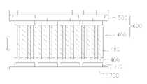
- FIG. 7shows a probe card adapted for wafer testing, being a conductive film coupling with a panel.
- the conductive film 400can be attached to the bottom of a panel 500 by means of hooking, wedging or adhering, by which a conductive film type probe card 600 can be formed.
- the panel 500is electrically connected to a circuit board which is used for driving the panel 500 to move, the moving panel will bring along the conductive film 400 to move and thus to engage or disengage with bonding pads 710 of a wafer 700 .
- the array of parallel-arranged linear micro-threads 460 shown in FIG. 7is only an exemplary embodiment of the invention, which is not limited thereby.
- the conductive film 400 disclosed in the inventionis characterized in that: as each metal micro-thread 460 is wrapped inside the insulating film 480 while having its two ends extending outside the two opposite edges of the insulating film 480 by a specific length, as shown in FIG. 7 , such design is beneficiary for the micro-thread to engage with the bonding pads 710 . Nevertheless, since the insulating film 480 is flexible, even when the micro-thread 460 are completely wrapped inside the insulating film 480 , the panel 500 can be compressed for extruding the micro-threads 460 so as to facilitate the same to engage with the bonding pads 710 .
- micro-thread unit 490is manufacturing by the use of many micro/nano-technologies, such as micro/nano-scaled polymer film formation, LIGA process, and micro electroforming technology and the like.
- Micro-threads 460 of various aspect ratioscan be formed, which is configured with a wire diameter no larger than 4 ⁇ m; and the pitch between any two neighboring micro-threads is not larger than 10 ⁇ m. It is known that the dimension of a common bonding pad 710 is about 70 ⁇ 70 ⁇ m. Thus, the so-formed probe card is capable of engaging more than one pin to one bonding pad 710 , even when the size of future bonding pad is reduced to smaller then 25 ⁇ m.
- the probe card of the inventionis capable of being adapted for wafers of various bonding pad arrangements, that there is no need to design probe cards specifically for different IC chips.
- the method of the presentis especially good for manufacturing probe cards for future full wafer testing since it adopts flexible film design, as describe hereinbefore, so that no only it requires no assembly, but also it do not need to worry about the pin count and area limitations troubling those conventional probe cards.
- the film type probe card disclosed in the inventionis a low-cost, ease-to-maintain probe card with large area detection ability that not only is capable of engaging more than one pin to a bonding pad, but also is adapted for wafers of various bonding pad arrangements. It is emphasized that the process for manufacturing a conductive film, as shown sequentially in FIG. 4A to FIG. 4H , is only an exemplary embodiment of the invention. Other variations using micro/nano-technologies, such as micro/nano-scaled polymer film formation, LIGA process, and micro electroforming technology and the like, are not to be regarded as a departure from the spirit and scope of the invention.
Landscapes
- Physics & Mathematics (AREA)
- General Physics & Mathematics (AREA)
- Measuring Leads Or Probes (AREA)
- Testing Or Measuring Of Semiconductors Or The Like (AREA)
- Non-Insulated Conductors (AREA)
Abstract
Description
- The present invention relates to a method for manufacturing a conductive film and a probe card using the same, and more particularly, to a probe card capable of engaging more than one pin to a bonding pad that is adapted for wafer of various bonding pad arrangement.
- A probe card is an interface between an electronic test system and a semiconductor wafer. Its purpose is to provide an electrical path between the test system and the circuits on the wafer, thereby permitting the testing and validation of the circuits at the wafer level, usually before they are diced and packaged. That is, before hundreds of IC chips fixed on a wafer are diced into chips with a few square millimeters, “Wafer Test” should be performed utilizing such probe card to check quality of IC chips and thus screen out defectives. However, as semiconductor manufacturers continue to shrink die geometries, which makes the task of on-wafer testing increasingly more difficult since pitches between bonding pads are becoming minute. Probe card with innovative solutions, which can perform a wafer level probing test on multiple chips on a wafer at once or even on the whole wafer, are required to meet the semiconductor industry's test needs so as to ensure higher accuracy and repeatable wafer testing and thus increase yield as well as lower cost.
- Probe cards are broadly classified into cantilever type, vertical type, and MEMS (Micro Electro-Mechanical System) type depending on shape and forms of contact elements. The cantilever type is represented by the epoxy ring probe card, the vertical type is represented by the cobra probe card, and the MEMS type is usually used for DRAM (dynamic random access memory) testing.
- Among which, although the cantilever type probe cards are usually designed with fine pitch as small as 40 μm, it is only suitable for testing those
wafers bonding pads FIG. 1 andFIG. 2 , so that the pin count of such cantilever type probe card is limited and thus it is classified as low-end probe card. As for the vertical type probe card, it is originated from a manufacturing process disclosed at 1997 in U.S. Pat. No. 4,027,925, entitled “Contact for an electrical contactor assembly”, in which a vertical probe head disclosed has each of it's probes buckle or deflect when a predetermined axial load is applied thereto for enabling the same force to be exerted on each of a plurality of pads on a semiconductor chip as it is being tested. However, although such vertical type probe card is adapted for testing wafers300 with a plurality of bonding pads arranged as arrays and is classified as high-end probe card with high pin count, it is bottlenecked for designing such vertical type probe card with pitch as small as 100 μm. Therefore, such vertical type probe cards are only good for testing flip chip packaged IC. - It is noted that each pin in the foregoing two types of probe card are manufactured in a manner that it is fixed onto a PCB (printed circuit board) manually. Thus, their manufacturing cost is closely related to their pin counts, i.e. the higher the pin count is, the higher the manufacturing cost will be.
- The MEMS type probe card for DRAM is exemplified in the U.S. Pat. No. 5,476,211, entitled “Method of manufacturing electrical contacts, using a sacrificial member”, and the U.S. Pat. No. 5,476,211, entitled “Method of making and using lithographic contact springs”. However, it is disadvantageous in that its manufacturing process is complex and it is bottlenecked for designing such MEMS type probe card with pitch smaller than 70 μm, thereby, such MEMS type probe can be very expensive. In addition, it is limited to be used for testing wafers with bonding pad arrangement similar to that shown in
FIG. 1 . - Over all, those currently available probe cards are all capable of performing wafer testing in a “one pin corresponding to one pad” manner, so that it is required to redesign its pin configuration for matching wafers of various bonding pad arrangements. In addition, the pin pitches of those currently available probe cards are limited by their manufacturing processes, which might not be able to meet the challenge of ultra fine pitch up to those smaller than 70 μm, high pin counts and full wafer testing. There are already some studies trying to deal with shortcomings, such as high cost, pins of large volume, and restricted shape, etc, that are common for those conventional probe cards as they are usually manufactured by mold casting, drawing or roll milling. Such studies can be exemplified by the probe card manufacturing methods disclosed in TW Pat. No. 90107441 and TW Pat. No. 93107026. However, such studies still limited in the aforesaid “one pin corresponding to one pad” manner, and thus suffer the same shortcomings. Therefore, it is in need of a new probe card that not only is not troubled by the aforesaid fine pitch bottleneck, but also can be configured with high pin count and manufactured at low cost.
- The object of the present invention is to provide a method for manufacturing a conductive film and a probe card using the same, that can produce a low-cost, ease-to-maintain probe card with large area detection ability that is adapted for wafers of various bonding pad arrangements.
- To achieve the above object, the present invention provides a method for manufacturing a conductive film, comprising the steps of: sequentially forming a first insulating layer, a first metal layer and a photoresist layer on a substrate; forming a plurality of grooves on the photoresist layer while enabling each groove to channel through two opposite edges of the photoresist layer; forming a second metal layer inside each groove while electrically coupling the second metal layers with the first metal layer; removing the photoresist layer; removing the portion of the first metal layer that is not covered by the second metal layers so as to form an array of metal micro-threads; forming a second insulating layer on the array of metal micro-threads for incorporating the second insulating layer with the first insulating layer to from an insulating film wrapping the metal micro-threads; peering off the insulating film along with the micro-threads wrapped therein from the substrate so as to form an metal micro-thread unit; and stacking and adhering a plurality of the aforesaid metal micro-thread units to form a conductive film of a specific thickness.
- In an exemplary embodiment of the invention, the insulating film is substantially a polymer thin film of high dielectric constant, being made of a material such as polydimethylsiloxane (PDMA) or polyimide (PI).
- In an exemplary embodiment of the invention, the metal micro-thread is made of a material of high conductivity and high strength, such as Ni—Co alloy.
- In an exemplary embodiment of the invention, the aspect ratio of each micro-thread is high and is configured with a wire diameter no larger than 4 μm.
- In an exemplary embodiment of the invention, the pitch between any two neighboring micro-threads is not larger than 10 μm.
- In an exemplary embodiment of the invention, the cross section of each micro-thread can be shaped like a rectangle or a square.
- In an exemplary embodiment of the invention, the stacking and adhering of the plural micro-thread units into a film of the specific thickness is performed by a surface processing and mechanical healing procedure.
- In an exemplary embodiment of the invention, the mechanical healing procedure in performed in a vacuum environment.
- In an exemplary embodiment of the invention, the micro-threads in the stacking micro-thread units are arranged parallel to each other.
- In an exemplary embodiment of the invention, the method for manufacturing a conductive film further comprises a step of: dicing the conductive film into pieces of a specific dimension; and the dicing can be performed by the use of an energy beam, such as laser beam, ion beam and plasma beam, etc.
- In an exemplary embodiment of the invention, the substrate is a silicon wafer.
- In an exemplary embodiment of the invention, the first and the second metal layers are nano-scaled thin metal film, being made of a material selected from the group consisting of nickel, cooper and a Ni—Co ally of high conductivity and high strength.
- In an exemplary embodiment of the invention, the plural grooves on the photoresist layer is formed by a means selected from the group consisting of: a means of direct etching using an energy beam, and a means of indirect etching through a mask using an energy beam; and such energy beam can be a laser beam, an ion beam or a plasma beam.
- In an exemplary embodiment of the invention, the plural grooves are arranged parallel to each other in a unidirectional and single-layered manner.
- Moreover, to achieve the above object, the present invention provides a conductive film, being formed by adhering and stacking a plurality of micro-thread units into a film with a specific thickness; wherein each of the plural micro-thread units is substantially an array of micro-threads, wrapped in an insulating film while enabling the micro-threads in the array being arranged in a unidirectional and single-layered manner.
- In addition, to achieve the above object, the present invention provides a conductive film type probe card, comprising: at least a conductive film, each being formed by adhering and stacking a plurality of micro-thread units into a film with a specific thickness; a panel, provided for the at least one conductive film to coupled therewith; and a circuit board, for driving the panel; wherein each of the plural micro-thread units is substantially an array of micro-threads, wrapped in an insulating film while enabling the micro-threads in the array being arranged in a unidirectional and single-layered manner.
- Further scope of applicability of the present application will become more apparent from the detailed description given hereinafter. However, it should be understood that the detailed description and specific examples, while indicating preferred embodiments of the invention, are given by way of illustration only, since various changes and modifications within the spirit and scope of the invention will become apparent to those skilled in the art from this detailed description.
- The present invention will become more fully understood from the detailed description given herein below and the accompanying drawings which are given by way of illustration only, and thus are not limitative of the present invention and wherein:
FIG. 1 toFIG. 3 show three different bonding pad arrangements on a wafer in respective.FIG. 4A toFIG. 4H show sequentially the manufacturing of a conductive film, each representing a step in the manufacturing process.FIG. 5 is a schematic diagram showing a photoresist layer of a conductive film having a plurality of grooves formed therein.FIG. 6 is a cross sectional view of a diced conductive film.FIG. 7 shows a probe card adapted for wafer testing, being a conductive film coupling with a panel.- For your esteemed members of reviewing committee to further understand and recognize the fulfilled functions and structural characteristics of the invention, several exemplary embodiments cooperating with detailed description are presented as the follows.
- Please refer to
FIG. 4A toFIG. 4H , which show sequentially the manufacturing of a conductive film, each representing a step in the manufacturing process. The manufacturing of the conductive film makes use of many micro/nano-technologies, such as micro/nano-scaled polymer film formation, LIGA process, and micro electroforming technology and the like. - In
FIG. 4A , asilicon substrate 410 is provided, on which a micro scaled polymer film, made of a material such as PDMS or PI, is first being coated and used as a first insulatinglayer 420; and then on the first insulatinglayer 420, a nano-scaled metal layer, made of a metal such as nickel or copper, is formed by sputtering or electroless plating and used as afirst metal layer 430; and thereafter, on thefirst metal layer 430, aphotoresist layer 440 is formed. - In
FIG. 4B , a plurality ofgrooves 441 on thephotoresist layer 440 by the use of a energy beam, such as a laser beam, an ion beam, or a plasma beam, in a direct etching manner or through a mask. Please refer toFIG. 5 , is a schematic diagram showing a photoresist layer of a conductive film having a plurality of grooves formed therein. As shown inFIG. 5 , theplural grooves 441 are arranged parallel to each other in a unidirectional and single-layered manner while enabling eachgroove 441 to channel through two opposite edges of thephotoresist layer 440. - In
FIG. 4C , asecond metal layer 450 is formed in eachgroove 441 by electroplating. It is noted that thesecond metal film 450 is made of a metal of high conductivity and high strength, such as a Ni—Co alloy; and it is configured for electrically coupling with thefirst metal layer 430. - In
FIG. 4D , thephotoresist layer 440 is removed. - In
FIG. 4E , the portion of thefirst metal layer 430 that is not covered by the second metal layers450 is removed by etching so as to form a plurality ofmetal micro-threads 460. As shown inFIG. 4D , the cross section of each micro-thread460 is shaped like a rectangle. However, it can be shaped like a square or other geometrical shapes as it is dependent on the thicknesses of first metal and the second metal layers430,450. - In
FIG. 4F , theplural micro-threads 460 is covered by a second insulatinglayer 470 while enabling the second insulatinglayer 470 to combine with the first insulatinglayer 420 to form an insulatingfilm 480 in a manner that the insulating film481 wraps theplural micro-threads 460 therein. - In
FIG. 4G , the insulatingfilm 480 is detached from thesubstrate 410 and along with it, theplural micro-threads 460 are also being peered, by which ametal micro-thread unit 490 is established. The aspect ratio of each micro-thread460 is high and is configured with a wire diameter no larger than 4 μm. In addition, the pitch between any two neighboring micro-threads is not larger than 10 μm. - In
FIG. 4H , after the formation of such metal micro-thread units is completed, aconductive film 400 of a specific thickness, formed by the adhering and stacking of at least one suchmetal micro-thread unit 490 in a vacuum environment by the use of surface processing and mechanical healing, is formed. As shown inFIG. 4H andFIG. 6 , the micro-threads460 in the stackingmicro-thread units 490 are arranged parallel to each other. Furthermore, the so-formedconductive film 400 can be diced intopieces 400aof a specific dimension; and the dicing can be performed by the use of an energy beam, such as laser beam, ion beam and plasma beam, etc. - Please refer to
FIG. 7 , which shows a probe card adapted for wafer testing, being a conductive film coupling with a panel. It is noted that theconductive film 400 can be attached to the bottom of apanel 500 by means of hooking, wedging or adhering, by which a conductive filmtype probe card 600 can be formed. As thepanel 500 is electrically connected to a circuit board which is used for driving thepanel 500 to move, the moving panel will bring along theconductive film 400 to move and thus to engage or disengage withbonding pads 710 of awafer 700. However, the array of parallel-arrangedlinear micro-threads 460 shown inFIG. 7 is only an exemplary embodiment of the invention, which is not limited thereby. Theconductive film 400 disclosed in the invention is characterized in that: as eachmetal micro-thread 460 is wrapped inside the insulatingfilm 480 while having its two ends extending outside the two opposite edges of the insulatingfilm 480 by a specific length, as shown inFIG. 7 , such design is beneficiary for the micro-thread to engage with thebonding pads 710. Nevertheless, since the insulatingfilm 480 is flexible, even when the micro-thread460 are completely wrapped inside the insulatingfilm 480, thepanel 500 can be compressed for extruding themicro-threads 460 so as to facilitate the same to engage with thebonding pads 710. - Moreover, as the
metal micro-thread unit 490 is manufacturing by the use of many micro/nano-technologies, such as micro/nano-scaled polymer film formation, LIGA process, and micro electroforming technology and the like.Micro-threads 460 of various aspect ratios can be formed, which is configured with a wire diameter no larger than 4 μm; and the pitch between any two neighboring micro-threads is not larger than 10 μm. It is known that the dimension of acommon bonding pad 710 is about 70×70 μm. Thus, the so-formed probe card is capable of engaging more than one pin to onebonding pad 710, even when the size of future bonding pad is reduced to smaller then 25 μm. Moreover, the probe card of the invention is capable of being adapted for wafers of various bonding pad arrangements, that there is no need to design probe cards specifically for different IC chips. Yet, the method of the present is especially good for manufacturing probe cards for future full wafer testing since it adopts flexible film design, as describe hereinbefore, so that no only it requires no assembly, but also it do not need to worry about the pin count and area limitations troubling those conventional probe cards. - To sum up, the film type probe card disclosed in the invention is a low-cost, ease-to-maintain probe card with large area detection ability that not only is capable of engaging more than one pin to a bonding pad, but also is adapted for wafers of various bonding pad arrangements. It is emphasized that the process for manufacturing a conductive film, as shown sequentially in
FIG. 4A toFIG. 4H , is only an exemplary embodiment of the invention. Other variations using micro/nano-technologies, such as micro/nano-scaled polymer film formation, LIGA process, and micro electroforming technology and the like, are not to be regarded as a departure from the spirit and scope of the invention. - The invention being thus described, it will be obvious that the same may be varied in many ways. Such variations are not to be regarded as a departure from the spirit and scope of the invention, and all such modifications as would be obvious to one skilled in the art are intended to be included within the scope of the following claims.
Claims (20)
Applications Claiming Priority (3)
| Application Number | Priority Date | Filing Date | Title |
|---|---|---|---|
| TW096137385ATWI360182B (en) | 2007-10-05 | 2007-10-05 | Method for making a conductive film |
| TW096137385 | 2007-10-05 | ||
| TW96137385A | 2007-10-05 |
Publications (2)
| Publication Number | Publication Date |
|---|---|
| US20090091343A1true US20090091343A1 (en) | 2009-04-09 |
| US7710132B2 US7710132B2 (en) | 2010-05-04 |
Family
ID=40522723
Family Applications (1)
| Application Number | Title | Priority Date | Filing Date |
|---|---|---|---|
| US12/032,169Expired - Fee RelatedUS7710132B2 (en) | 2007-10-05 | 2008-02-15 | Method for making a conductive film and a probe card using the same |
Country Status (3)
| Country | Link |
|---|---|
| US (1) | US7710132B2 (en) |
| JP (1) | JP4903668B2 (en) |
| TW (1) | TWI360182B (en) |
Cited By (15)
| Publication number | Priority date | Publication date | Assignee | Title |
|---|---|---|---|---|
| US20090066352A1 (en)* | 2006-10-16 | 2009-03-12 | Formfactor, Inc. | Making And Using Carbon Nanotube Probes |
| US20090197484A1 (en)* | 2007-10-13 | 2009-08-06 | Formfactor, Inc. | Carbon nanotube spring contact structures with mechanical and electrical components |
| US20100083489A1 (en)* | 2006-10-16 | 2010-04-08 | Formfactor, Inc. | Carbon nanotube columns and methods of making and using carbon nanotube columns as probes |
| US20100112828A1 (en)* | 2006-08-21 | 2010-05-06 | Formfactor, Inc. | Carbon nanotube contact structures |
| US20100164517A1 (en)* | 2008-12-29 | 2010-07-01 | Industrial Technology Research Institute | Conductive film structure, fabrication method thereof, and conductive film type probe device for ics |
| US20100216273A1 (en)* | 2009-02-20 | 2010-08-26 | Tsinghua University | Method for fabricating carbon nanotube array sensor |
| US20100253375A1 (en)* | 2009-04-03 | 2010-10-07 | Formfactor, Inc. | Anchoring carbon nanotube columns |
| US20100252317A1 (en)* | 2009-04-03 | 2010-10-07 | Formfactor, Inc. | Carbon nanotube contact structures for use with semiconductor dies and other electronic devices |
| US8638113B2 (en) | 2005-06-24 | 2014-01-28 | Formfactor, Inc. | Temporary planar electrical contact device and method using vertically-compressible nanotube contact structures |
| US8872176B2 (en) | 2010-10-06 | 2014-10-28 | Formfactor, Inc. | Elastic encapsulated carbon nanotube based electrical contacts |
| US20180003737A1 (en)* | 2012-12-26 | 2018-01-04 | Translarity, Inc. | Designed asperity contactors, including nanospikes, for semiconductor test, and associated systems and methods |
| WO2021133558A1 (en)* | 2019-12-24 | 2021-07-01 | Teradyne, Inc. | Probe card assembly in automated test equipment |
| US11162980B2 (en) | 2019-12-24 | 2021-11-02 | Teradyne, Inc. | Coaxial via arrangement in probe card for automated test equipment |
| US11333683B2 (en) | 2019-12-24 | 2022-05-17 | Teradyne, Inc. | Transposed via arrangement in probe card for automated test equipment |
| US11340260B2 (en) | 2019-12-24 | 2022-05-24 | Teradyne, Inc. | Probe card pad geometry in automated test equipment |
Families Citing this family (1)
| Publication number | Priority date | Publication date | Assignee | Title |
|---|---|---|---|---|
| KR101039338B1 (en)* | 2010-01-25 | 2011-06-08 | 주식회사 코디에스 | Probe unit for extreme fine pitch inspection |
Citations (5)
| Publication number | Priority date | Publication date | Assignee | Title |
|---|---|---|---|---|
| US4027925A (en)* | 1974-05-13 | 1977-06-07 | Black Chester A | Detachable road protecting device for tracked vehicles |
| US4027935A (en)* | 1976-06-21 | 1977-06-07 | International Business Machines Corporation | Contact for an electrical contactor assembly |
| US5476211A (en)* | 1993-11-16 | 1995-12-19 | Form Factor, Inc. | Method of manufacturing electrical contacts, using a sacrificial member |
| US6433565B1 (en)* | 2001-05-01 | 2002-08-13 | Lsi Logic Corporation | Test fixture for flip chip ball grid array circuits |
| US6581276B2 (en)* | 2000-04-04 | 2003-06-24 | Amerasia International Technology, Inc. | Fine-pitch flexible connector, and method for making same |
Family Cites Families (5)
| Publication number | Priority date | Publication date | Assignee | Title |
|---|---|---|---|---|
| JPS61240511A (en)* | 1985-04-18 | 1986-10-25 | 松下電器産業株式会社 | Manufacture of anisotropic conducting adhesive sheet |
| JP3737899B2 (en)* | 1999-01-29 | 2006-01-25 | 日東電工株式会社 | Semiconductor element inspection method and anisotropic conductive film therefor |
| JP3543765B2 (en)* | 2000-12-28 | 2004-07-21 | Jsr株式会社 | Probe device for wafer inspection |
| TW517320B (en) | 2001-03-27 | 2003-01-11 | Chipmos Technologies Inc | A method of manufacturing the probe needles |
| CN100536231C (en)* | 2002-03-20 | 2009-09-02 | 日本压着端子制造株式会社 | Anisotropic conductive sheet and preparation method thereof |
- 2007
- 2007-10-05TWTW096137385Apatent/TWI360182B/ennot_activeIP Right Cessation
- 2007-10-30JPJP2007281546Apatent/JP4903668B2/ennot_activeExpired - Fee Related
- 2008
- 2008-02-15USUS12/032,169patent/US7710132B2/ennot_activeExpired - Fee Related
Patent Citations (5)
| Publication number | Priority date | Publication date | Assignee | Title |
|---|---|---|---|---|
| US4027925A (en)* | 1974-05-13 | 1977-06-07 | Black Chester A | Detachable road protecting device for tracked vehicles |
| US4027935A (en)* | 1976-06-21 | 1977-06-07 | International Business Machines Corporation | Contact for an electrical contactor assembly |
| US5476211A (en)* | 1993-11-16 | 1995-12-19 | Form Factor, Inc. | Method of manufacturing electrical contacts, using a sacrificial member |
| US6581276B2 (en)* | 2000-04-04 | 2003-06-24 | Amerasia International Technology, Inc. | Fine-pitch flexible connector, and method for making same |
| US6433565B1 (en)* | 2001-05-01 | 2002-08-13 | Lsi Logic Corporation | Test fixture for flip chip ball grid array circuits |
Cited By (22)
| Publication number | Priority date | Publication date | Assignee | Title |
|---|---|---|---|---|
| US8638113B2 (en) | 2005-06-24 | 2014-01-28 | Formfactor, Inc. | Temporary planar electrical contact device and method using vertically-compressible nanotube contact structures |
| US20100112828A1 (en)* | 2006-08-21 | 2010-05-06 | Formfactor, Inc. | Carbon nanotube contact structures |
| US7731503B2 (en) | 2006-08-21 | 2010-06-08 | Formfactor, Inc. | Carbon nanotube contact structures |
| US8130007B2 (en) | 2006-10-16 | 2012-03-06 | Formfactor, Inc. | Probe card assembly with carbon nanotube probes having a spring mechanism therein |
| US20100083489A1 (en)* | 2006-10-16 | 2010-04-08 | Formfactor, Inc. | Carbon nanotube columns and methods of making and using carbon nanotube columns as probes |
| US20090066352A1 (en)* | 2006-10-16 | 2009-03-12 | Formfactor, Inc. | Making And Using Carbon Nanotube Probes |
| US8354855B2 (en) | 2006-10-16 | 2013-01-15 | Formfactor, Inc. | Carbon nanotube columns and methods of making and using carbon nanotube columns as probes |
| US20090197484A1 (en)* | 2007-10-13 | 2009-08-06 | Formfactor, Inc. | Carbon nanotube spring contact structures with mechanical and electrical components |
| US8149007B2 (en) | 2007-10-13 | 2012-04-03 | Formfactor, Inc. | Carbon nanotube spring contact structures with mechanical and electrical components |
| US20100164517A1 (en)* | 2008-12-29 | 2010-07-01 | Industrial Technology Research Institute | Conductive film structure, fabrication method thereof, and conductive film type probe device for ics |
| US20100216273A1 (en)* | 2009-02-20 | 2010-08-26 | Tsinghua University | Method for fabricating carbon nanotube array sensor |
| US9068923B2 (en)* | 2009-02-20 | 2015-06-30 | Tsinghua University | Method for fabricating carbon nanotube array sensor |
| US20100252317A1 (en)* | 2009-04-03 | 2010-10-07 | Formfactor, Inc. | Carbon nanotube contact structures for use with semiconductor dies and other electronic devices |
| US8272124B2 (en) | 2009-04-03 | 2012-09-25 | Formfactor, Inc. | Anchoring carbon nanotube columns |
| US20100253375A1 (en)* | 2009-04-03 | 2010-10-07 | Formfactor, Inc. | Anchoring carbon nanotube columns |
| US8872176B2 (en) | 2010-10-06 | 2014-10-28 | Formfactor, Inc. | Elastic encapsulated carbon nanotube based electrical contacts |
| US20180003737A1 (en)* | 2012-12-26 | 2018-01-04 | Translarity, Inc. | Designed asperity contactors, including nanospikes, for semiconductor test, and associated systems and methods |
| WO2021133558A1 (en)* | 2019-12-24 | 2021-07-01 | Teradyne, Inc. | Probe card assembly in automated test equipment |
| US11162980B2 (en) | 2019-12-24 | 2021-11-02 | Teradyne, Inc. | Coaxial via arrangement in probe card for automated test equipment |
| US11215641B2 (en) | 2019-12-24 | 2022-01-04 | Teradyne, Inc. | Probe card assembly in automated test equipment |
| US11333683B2 (en) | 2019-12-24 | 2022-05-17 | Teradyne, Inc. | Transposed via arrangement in probe card for automated test equipment |
| US11340260B2 (en) | 2019-12-24 | 2022-05-24 | Teradyne, Inc. | Probe card pad geometry in automated test equipment |
Also Published As
| Publication number | Publication date |
|---|---|
| US7710132B2 (en) | 2010-05-04 |
| TWI360182B (en) | 2012-03-11 |
| JP4903668B2 (en) | 2012-03-28 |
| JP2009094442A (en) | 2009-04-30 |
| TW200917366A (en) | 2009-04-16 |
Similar Documents
| Publication | Publication Date | Title |
|---|---|---|
| US7710132B2 (en) | Method for making a conductive film and a probe card using the same | |
| US7306493B2 (en) | Interconnection device for a printed circuit board, a method of manufacturing the same, and an interconnection assembly having the same | |
| US6922069B2 (en) | Needle assembly of probe card | |
| US7479237B2 (en) | Method of fabricating vertical probe head | |
| JP4414502B2 (en) | Probing card | |
| US20130299221A1 (en) | Space transformer for probe card and method of manufacturing the same | |
| US8710857B2 (en) | High frequency vertical spring probe | |
| JP2001056345A (en) | Probing card and its manufacture | |
| KR101168147B1 (en) | Probe pin for probe card and manufacturing method thereof | |
| KR100980369B1 (en) | Probe needle structure of the probe card and its manufacturing method | |
| US20240053382A1 (en) | Probe pin and method of manufacturing probe pin | |
| KR101638228B1 (en) | Fabrication method of probe pin capable of being used for fine pitch | |
| TW202342993A (en) | The electro-conductive contact pin and test device having the same | |
| US20090278561A1 (en) | Probe card having redistributed wiring probe needle structure and probe card module using the same | |
| KR101990458B1 (en) | Probe card and method for manufacturing the same | |
| US11555830B2 (en) | Small pitch integrated knife edge temporary bonding microstructures | |
| KR20230032060A (en) | The Electro-conductive Contact Pin and Vertical Probe Card Having The Same | |
| KR101209068B1 (en) | Probe needle and probe card using the same | |
| WO2013084874A1 (en) | Membrane sheet with bumps for probe card, probe card and method for manufacturing membrane sheet with bumps for probe card | |
| JP2009257910A (en) | Double elastic mechanism probe card and its method for manufacturing | |
| US20240272200A1 (en) | Probe card for fine pitch circuit probe testing of semiconductor integrated circuit devices and methods of forming the same | |
| KR100980002B1 (en) | Probe Structures and Manufacturing Method Thereof | |
| CN112710877A (en) | Metal probe structure and manufacturing method thereof | |
| KR20030033206A (en) | Probe micro-structure | |
| KR20230049214A (en) | The Electro-conductive Contact Pin and Testing Device Having The Same |
Legal Events
| Date | Code | Title | Description |
|---|---|---|---|
| AS | Assignment | Owner name:INDUSTRIAL TECHNOLOGY RESEARCH INSTITUTE, TAIWAN Free format text:ASSIGNMENT OF ASSIGNORS INTEREST;ASSIGNORS:WU, TUNG-CHUAN;CHOU, MIN-CHIEH;LIN, HUNG-YI;REEL/FRAME:020517/0360;SIGNING DATES FROM 20071120 TO 20071121 Owner name:INDUSTRIAL TECHNOLOGY RESEARCH INSTITUTE,TAIWAN Free format text:ASSIGNMENT OF ASSIGNORS INTEREST;ASSIGNORS:WU, TUNG-CHUAN;CHOU, MIN-CHIEH;LIN, HUNG-YI;SIGNING DATES FROM 20071120 TO 20071121;REEL/FRAME:020517/0360 | |
| FEPP | Fee payment procedure | Free format text:PAYOR NUMBER ASSIGNED (ORIGINAL EVENT CODE: ASPN); ENTITY STATUS OF PATENT OWNER: LARGE ENTITY | |
| STCF | Information on status: patent grant | Free format text:PATENTED CASE | |
| FPAY | Fee payment | Year of fee payment:4 | |
| MAFP | Maintenance fee payment | Free format text:PAYMENT OF MAINTENANCE FEE, 8TH YEAR, LARGE ENTITY (ORIGINAL EVENT CODE: M1552) Year of fee payment:8 | |
| FEPP | Fee payment procedure | Free format text:MAINTENANCE FEE REMINDER MAILED (ORIGINAL EVENT CODE: REM.); ENTITY STATUS OF PATENT OWNER: LARGE ENTITY | |
| LAPS | Lapse for failure to pay maintenance fees | Free format text:PATENT EXPIRED FOR FAILURE TO PAY MAINTENANCE FEES (ORIGINAL EVENT CODE: EXP.); ENTITY STATUS OF PATENT OWNER: LARGE ENTITY | |
| STCH | Information on status: patent discontinuation | Free format text:PATENT EXPIRED DUE TO NONPAYMENT OF MAINTENANCE FEES UNDER 37 CFR 1.362 | |
| FP | Lapsed due to failure to pay maintenance fee | Effective date:20220504 |