US20090091009A1 - Stackable integrated circuit package - Google Patents
Stackable integrated circuit packageDownload PDFInfo
- Publication number
- US20090091009A1 US20090091009A1US11/866,788US86678807AUS2009091009A1US 20090091009 A1US20090091009 A1US 20090091009A1US 86678807 AUS86678807 AUS 86678807AUS 2009091009 A1US2009091009 A1US 2009091009A1
- Authority
- US
- United States
- Prior art keywords
- die
- lead fingers
- integrated circuit
- paddle
- encapsulant material
- Prior art date
- Legal status (The legal status is an assumption and is not a legal conclusion. Google has not performed a legal analysis and makes no representation as to the accuracy of the status listed.)
- Abandoned
Links
Images


Classifications
- H—ELECTRICITY
- H01—ELECTRIC ELEMENTS
- H01L—SEMICONDUCTOR DEVICES NOT COVERED BY CLASS H10
- H01L23/00—Details of semiconductor or other solid state devices
- H01L23/48—Arrangements for conducting electric current to or from the solid state body in operation, e.g. leads, terminal arrangements ; Selection of materials therefor
- H01L23/488—Arrangements for conducting electric current to or from the solid state body in operation, e.g. leads, terminal arrangements ; Selection of materials therefor consisting of soldered or bonded constructions
- H01L23/495—Lead-frames or other flat leads
- H01L23/49575—Assemblies of semiconductor devices on lead frames
- H—ELECTRICITY
- H01—ELECTRIC ELEMENTS
- H01L—SEMICONDUCTOR DEVICES NOT COVERED BY CLASS H10
- H01L23/00—Details of semiconductor or other solid state devices
- H01L23/48—Arrangements for conducting electric current to or from the solid state body in operation, e.g. leads, terminal arrangements ; Selection of materials therefor
- H01L23/488—Arrangements for conducting electric current to or from the solid state body in operation, e.g. leads, terminal arrangements ; Selection of materials therefor consisting of soldered or bonded constructions
- H01L23/495—Lead-frames or other flat leads
- H01L23/49541—Geometry of the lead-frame
- H01L23/49548—Cross section geometry
- H01L23/49551—Cross section geometry characterised by bent parts
- H01L23/49555—Cross section geometry characterised by bent parts the bent parts being the outer leads
- H—ELECTRICITY
- H01—ELECTRIC ELEMENTS
- H01L—SEMICONDUCTOR DEVICES NOT COVERED BY CLASS H10
- H01L25/00—Assemblies consisting of a plurality of semiconductor or other solid state devices
- H01L25/03—Assemblies consisting of a plurality of semiconductor or other solid state devices all the devices being of a type provided for in a single subclass of subclasses H10B, H10D, H10F, H10H, H10K or H10N, e.g. assemblies of rectifier diodes
- H01L25/10—Assemblies consisting of a plurality of semiconductor or other solid state devices all the devices being of a type provided for in a single subclass of subclasses H10B, H10D, H10F, H10H, H10K or H10N, e.g. assemblies of rectifier diodes the devices having separate containers
- H01L25/105—Assemblies consisting of a plurality of semiconductor or other solid state devices all the devices being of a type provided for in a single subclass of subclasses H10B, H10D, H10F, H10H, H10K or H10N, e.g. assemblies of rectifier diodes the devices having separate containers the devices being integrated devices of class H10
- H—ELECTRICITY
- H01—ELECTRIC ELEMENTS
- H01L—SEMICONDUCTOR DEVICES NOT COVERED BY CLASS H10
- H01L2224/00—Indexing scheme for arrangements for connecting or disconnecting semiconductor or solid-state bodies and methods related thereto as covered by H01L24/00
- H01L2224/01—Means for bonding being attached to, or being formed on, the surface to be connected, e.g. chip-to-package, die-attach, "first-level" interconnects; Manufacturing methods related thereto
- H01L2224/26—Layer connectors, e.g. plate connectors, solder or adhesive layers; Manufacturing methods related thereto
- H01L2224/31—Structure, shape, material or disposition of the layer connectors after the connecting process
- H01L2224/32—Structure, shape, material or disposition of the layer connectors after the connecting process of an individual layer connector
- H01L2224/321—Disposition
- H01L2224/32135—Disposition the layer connector connecting between different semiconductor or solid-state bodies, i.e. chip-to-chip
- H01L2224/32145—Disposition the layer connector connecting between different semiconductor or solid-state bodies, i.e. chip-to-chip the bodies being stacked
- H—ELECTRICITY
- H01—ELECTRIC ELEMENTS
- H01L—SEMICONDUCTOR DEVICES NOT COVERED BY CLASS H10
- H01L2224/00—Indexing scheme for arrangements for connecting or disconnecting semiconductor or solid-state bodies and methods related thereto as covered by H01L24/00
- H01L2224/01—Means for bonding being attached to, or being formed on, the surface to be connected, e.g. chip-to-package, die-attach, "first-level" interconnects; Manufacturing methods related thereto
- H01L2224/42—Wire connectors; Manufacturing methods related thereto
- H01L2224/47—Structure, shape, material or disposition of the wire connectors after the connecting process
- H01L2224/48—Structure, shape, material or disposition of the wire connectors after the connecting process of an individual wire connector
- H01L2224/4805—Shape
- H01L2224/4809—Loop shape
- H01L2224/48091—Arched
- H—ELECTRICITY
- H01—ELECTRIC ELEMENTS
- H01L—SEMICONDUCTOR DEVICES NOT COVERED BY CLASS H10
- H01L2224/00—Indexing scheme for arrangements for connecting or disconnecting semiconductor or solid-state bodies and methods related thereto as covered by H01L24/00
- H01L2224/01—Means for bonding being attached to, or being formed on, the surface to be connected, e.g. chip-to-package, die-attach, "first-level" interconnects; Manufacturing methods related thereto
- H01L2224/42—Wire connectors; Manufacturing methods related thereto
- H01L2224/47—Structure, shape, material or disposition of the wire connectors after the connecting process
- H01L2224/48—Structure, shape, material or disposition of the wire connectors after the connecting process of an individual wire connector
- H01L2224/481—Disposition
- H01L2224/48151—Connecting between a semiconductor or solid-state body and an item not being a semiconductor or solid-state body, e.g. chip-to-substrate, chip-to-passive
- H01L2224/48221—Connecting between a semiconductor or solid-state body and an item not being a semiconductor or solid-state body, e.g. chip-to-substrate, chip-to-passive the body and the item being stacked
- H01L2224/48245—Connecting between a semiconductor or solid-state body and an item not being a semiconductor or solid-state body, e.g. chip-to-substrate, chip-to-passive the body and the item being stacked the item being metallic
- H01L2224/48247—Connecting between a semiconductor or solid-state body and an item not being a semiconductor or solid-state body, e.g. chip-to-substrate, chip-to-passive the body and the item being stacked the item being metallic connecting the wire to a bond pad of the item
- H—ELECTRICITY
- H01—ELECTRIC ELEMENTS
- H01L—SEMICONDUCTOR DEVICES NOT COVERED BY CLASS H10
- H01L2224/00—Indexing scheme for arrangements for connecting or disconnecting semiconductor or solid-state bodies and methods related thereto as covered by H01L24/00
- H01L2224/73—Means for bonding being of different types provided for in two or more of groups H01L2224/10, H01L2224/18, H01L2224/26, H01L2224/34, H01L2224/42, H01L2224/50, H01L2224/63, H01L2224/71
- H01L2224/732—Location after the connecting process
- H01L2224/73251—Location after the connecting process on different surfaces
- H01L2224/73265—Layer and wire connectors
- H—ELECTRICITY
- H01—ELECTRIC ELEMENTS
- H01L—SEMICONDUCTOR DEVICES NOT COVERED BY CLASS H10
- H01L2225/00—Details relating to assemblies covered by the group H01L25/00 but not provided for in its subgroups
- H01L2225/03—All the devices being of a type provided for in the same main group of the same subclass of class H10, e.g. assemblies of rectifier diodes
- H01L2225/10—All the devices being of a type provided for in the same main group of the same subclass of class H10, e.g. assemblies of rectifier diodes the devices having separate containers
- H01L2225/1005—All the devices being of a type provided for in the same main group of the same subclass of class H10, e.g. assemblies of rectifier diodes the devices having separate containers the devices being integrated devices of class H10
- H01L2225/1011—All the devices being of a type provided for in the same main group of the same subclass of class H10, e.g. assemblies of rectifier diodes the devices having separate containers the devices being integrated devices of class H10 the containers being in a stacked arrangement
- H01L2225/1017—All the devices being of a type provided for in the same main group of the same subclass of class H10, e.g. assemblies of rectifier diodes the devices having separate containers the devices being integrated devices of class H10 the containers being in a stacked arrangement the lowermost container comprising a device support
- H01L2225/1029—All the devices being of a type provided for in the same main group of the same subclass of class H10, e.g. assemblies of rectifier diodes the devices having separate containers the devices being integrated devices of class H10 the containers being in a stacked arrangement the lowermost container comprising a device support the support being a lead frame
- H—ELECTRICITY
- H01—ELECTRIC ELEMENTS
- H01L—SEMICONDUCTOR DEVICES NOT COVERED BY CLASS H10
- H01L24/00—Arrangements for connecting or disconnecting semiconductor or solid-state bodies; Methods or apparatus related thereto
- H01L24/01—Means for bonding being attached to, or being formed on, the surface to be connected, e.g. chip-to-package, die-attach, "first-level" interconnects; Manufacturing methods related thereto
- H01L24/42—Wire connectors; Manufacturing methods related thereto
- H01L24/47—Structure, shape, material or disposition of the wire connectors after the connecting process
- H01L24/48—Structure, shape, material or disposition of the wire connectors after the connecting process of an individual wire connector
- H—ELECTRICITY
- H01—ELECTRIC ELEMENTS
- H01L—SEMICONDUCTOR DEVICES NOT COVERED BY CLASS H10
- H01L2924/00—Indexing scheme for arrangements or methods for connecting or disconnecting semiconductor or solid-state bodies as covered by H01L24/00
- H01L2924/0001—Technical content checked by a classifier
- H01L2924/00014—Technical content checked by a classifier the subject-matter covered by the group, the symbol of which is combined with the symbol of this group, being disclosed without further technical details
- H—ELECTRICITY
- H01—ELECTRIC ELEMENTS
- H01L—SEMICONDUCTOR DEVICES NOT COVERED BY CLASS H10
- H01L2924/00—Indexing scheme for arrangements or methods for connecting or disconnecting semiconductor or solid-state bodies as covered by H01L24/00
- H01L2924/10—Details of semiconductor or other solid state devices to be connected
- H01L2924/102—Material of the semiconductor or solid state bodies
- H01L2924/1025—Semiconducting materials
- H01L2924/10251—Elemental semiconductors, i.e. Group IV
- H01L2924/10253—Silicon [Si]
- H—ELECTRICITY
- H01—ELECTRIC ELEMENTS
- H01L—SEMICONDUCTOR DEVICES NOT COVERED BY CLASS H10
- H01L2924/00—Indexing scheme for arrangements or methods for connecting or disconnecting semiconductor or solid-state bodies as covered by H01L24/00
- H01L2924/10—Details of semiconductor or other solid state devices to be connected
- H01L2924/11—Device type
- H01L2924/14—Integrated circuits
- H—ELECTRICITY
- H01—ELECTRIC ELEMENTS
- H01L—SEMICONDUCTOR DEVICES NOT COVERED BY CLASS H10
- H01L2924/00—Indexing scheme for arrangements or methods for connecting or disconnecting semiconductor or solid-state bodies as covered by H01L24/00
- H01L2924/15—Details of package parts other than the semiconductor or other solid state devices to be connected
- H01L2924/181—Encapsulation
- H—ELECTRICITY
- H01—ELECTRIC ELEMENTS
- H01L—SEMICONDUCTOR DEVICES NOT COVERED BY CLASS H10
- H01L2924/00—Indexing scheme for arrangements or methods for connecting or disconnecting semiconductor or solid-state bodies as covered by H01L24/00
- H01L2924/19—Details of hybrid assemblies other than the semiconductor or other solid state devices to be connected
- H01L2924/1901—Structure
- H01L2924/1904—Component type
- H01L2924/19041—Component type being a capacitor
Definitions
- This present subject matteris generally directed to the field of packaging integrated circuit devices, and, more particularly, to a stackable integrated circuit package.
- Integrated circuit technologyuses electrical devices, e.g., transistors, resistors, capacitors, etc., to formulate vast arrays of functional circuits.
- electrical devicese.g., transistors, resistors, capacitors, etc.
- the complexity of these circuitsrequires the use of an ever-increasing number of linked electrical devices so that the circuit may perform its intended function.
- the integrated circuitry dimensionsshrink.
- One challenge in the semiconductor industryis to develop improved methods for electrically connecting and packaging circuit devices which are fabricated on the same and/or on different wafers or chips. In general, it is desirable in the semiconductor industry to construct transistors which occupy less surface area on the silicon chip/die.
- DIPdual inline packages
- ZIPzig-zag inline packages
- SOJsmall outline J-bends
- TSOPthin small outline packages
- PLCCplastic leaded chip carriers
- SOICsmall outline integrated circuits
- PQFPplastic quad flat packs
- IDFinterdigitated leadframe
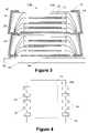
- FIGS. 1 and 2are cross-sectional views of illustrative embodiments of the stackable integrated circuit package disclosed herein;
- FIG. 3is a cross-sectional view depicting an illustrative example wherein a plurality of the stackable integrated circuit packages disclosed herein are operatively coupled to a printed circuit board;
- FIG. 4is a plan view of one illustrative embodiment of a stackable integrated circuit package disclosed herein;
- FIGS. 5A-4Gdepict one illustrative process flow that may be employed to form the stackable integrated circuit packages described herein.
- each of the packages 10 A, 10 Bare comprised of a plurality of integrated circuit die 12 that are coupled to one another by an adhesive or epoxy material 13 .
- the die 12are positioned above a paddle 20 of a traditional leadframe that is comprised of a plurality of leads or lead fingers 16 .
- the integrated circuit die 12are electrically coupled to the lead fingers 16 by illustrative wire bonds 18 .
- An encapsulant material 14e.g., mold compound, is formed around the various components described above. As can be observed in the drawings, the lead fingers 16 are bent or folded such that a portion 16 A of the lead finger 16 is positioned above a top surface 14 A of the encapsulant material 14 , e.g., mold compound.
- each of the packages 10 A, 10 Bhas a substantially planar bottom surface 17 .
- the packages 10 A, 10 Bare electrically coupled to one another through use of an electrically conductive adhesive or paste (not shown) positioned between the engaging portions of the lead fingers 16 on each package 10 A, 10 B.
- an electrically conductive adhesive or paste(not shown) positioned between the engaging portions of the lead fingers 16 on each package 10 A, 10 B.
- the bottom surface of such a packagee.g., package 10 A
- conductive paste or adhesivemay be applied to pads 52 on the printed circuit board 50 .
- a contact 54may be provided to the paddle 20 as well.
- FIGS. 1 and 2depict two illustrative stacked packages 10 A, 10 B, the present invention may be employed to stack any desired number of such packages together, e.g., 3-5 such packages.
- the subject matter disclosed hereinhas broad application and should not be considered as limited to the particular details disclosed herein.
- an air gap 23is provided between the packages 10 A, 10 B.
- a thermally conductive material 24may be formed or positioned so as to fill the air gap 23 , thereby providing increased heat transfer capabilities for the stacked packages 10 A, 10 B.
- the thermally conductive material 24may be comprised of a thermally conductive paste or tape, and it may have a thickness of approximately 100-200 ⁇ m. Such thermally conductive materials are well known to those skilled in the art.
- FIG. 4is a plan view of the top of the package 10 B in FIG. 1 .
- five illustrative lead fingers 16extend along only the sides of the integrated circuit die 12 .
- an actual productmay have a large number of such lead fingers 16 , however, for purposes of clarity, only ten such lead fingers 16 are shown in FIG. 4 .
- the lead fingers 16may extend around the entire perimeter of the package 10 B or only along the ends of the package 10 B.
- the illustrative arrangements depicted hereinshould not be considered to be a limitation of the present subject matter.
- FIGS. 5A-5Gdepict one illustrative process flow for forming a stackable package as described herein.
- a leadframe 30is positioned above a sacrificial support structure 26 .
- the leadframe 30comprises an illustrative die paddle 20 and a plurality of lead fingers 16 .
- the leadframe 30 depicted in the figuresis schematically depicted for purposes of explanation, the drawings are not to scale. In an actual device, the relative sizes of the various components and structures depicted herein may be different than what is depicted herein.
- the leadframe 30may be of traditional construction and it may be made from a variety of conductive materials, e.g., copper, Alloy 42, etc.
- the leadframe 30may be initially secured to the sacrificial structure 26 by using an adhesive material (not shown) or employing other similar techniques.
- a first die 12 Ais secured above the paddle 20 by an adhesive material (not shown).
- the die 12 Amay be electrically coupled to the paddle 20 via contact pads (not shown) on the bottom surface 15 of the die 12 A.
- the electrical connectionmay be established by applying a conductive paste or other similar materials (not shown).
- the die 12 Amay be coupled to the paddle 20 in such a manner as to promote heat transfer between the die 12 A and the paddle 20 .
- an adhesive designed to provide enhanced heat transfer capabilitiesmay be provided in an effort to increase the effectiveness of the heat transfer between the die 12 A and the paddle 20 .
- the die 12 Ais also electrically coupled to one or more of the lead fingers 16 .
- wire bonds 16may be employed for this purpose.
- the wire bond 16may be conductively coupled to bond pads (not shown) on the die 12 A and to the lead fingers 16 using known techniques.
- a layer of adhesive material 13is applied to the upper surface 19 of the die 12 A to attach another die 12 B, as shown in FIG. 5C .
- the processis essentially repeated to attach illustrative dies 12 C ( FIG. 5D) and 12D ( FIG. 5E ).
- the encapsulant material 14is formed around the structure depicted in FIG. 5E .
- the encapsulant material 14may be formed using a variety of known molding techniques, e.g., transfer molding, and materials, e.g., mold compound.
- the release angle of the side surfaces 14 Bmay vary depending upon the particular application. In one illustrative embodiment, the release angle may be approximately 8-20 degrees.
- the lead fingers 18are bent or folded such that portion 16 A of the lead finger 16 is positioned above a portion of the top surface 14 A of the encapsulant material 14 . Note that the angle of the folded lead finger 16 need not match the angle of the side surface 14 B of the encapsulant material 14 .
- the device depicted in FIG. 5Gmay thereafter be subjected to a variety of different tests to confirm its capabilities and/or ability to perform its intended function. In fact, if desired, such testing may be performed at various stages during the manufacture of the device. Ultimately, the objective is to only stack packages, e.g., packages 10 A, 10 B, that are “known good,” i.e., packages that have passed a desired set of electrical and/or mechanical integrity tests.
Landscapes
- Engineering & Computer Science (AREA)
- Power Engineering (AREA)
- Physics & Mathematics (AREA)
- Microelectronics & Electronic Packaging (AREA)
- Condensed Matter Physics & Semiconductors (AREA)
- General Physics & Mathematics (AREA)
- Computer Hardware Design (AREA)
- Geometry (AREA)
- Lead Frames For Integrated Circuits (AREA)
- Structures Or Materials For Encapsulating Or Coating Semiconductor Devices Or Solid State Devices (AREA)
Abstract
Description
- 1. Technical Field
- This present subject matter is generally directed to the field of packaging integrated circuit devices, and, more particularly, to a stackable integrated circuit package.
- 2. Description of the Related Art
- Integrated circuit technology uses electrical devices, e.g., transistors, resistors, capacitors, etc., to formulate vast arrays of functional circuits. The complexity of these circuits requires the use of an ever-increasing number of linked electrical devices so that the circuit may perform its intended function. As the number of transistors increases, the integrated circuitry dimensions shrink. One challenge in the semiconductor industry is to develop improved methods for electrically connecting and packaging circuit devices which are fabricated on the same and/or on different wafers or chips. In general, it is desirable in the semiconductor industry to construct transistors which occupy less surface area on the silicon chip/die.
- In the manufacture of semiconductor device assemblies, a single semiconductor die is most commonly incorporated into each sealed package. Many different package styles are used, including dual inline packages (DIP), zig-zag inline packages (ZIP), small outline J-bends (SOJ), thin small outline packages (TSOP), plastic leaded chip carriers (PLCC), small outline integrated circuits (SOIC), plastic quad flat packs (PQFP) and interdigitated leadframe (IDF). Some semiconductor device assemblies are connected to a substrate, such as a circuit board, prior to encapsulation. In some applications, integrated circuit die are packaged in a stacked configuration in an effort to reduce the plot space occupied by the integrated circuit product. Manufacturers are under constant pressure to reduce the size of the packaged integrated circuit device and to increase the packaging density in packaging integrated circuit devices.
- The present subject matter may be understood by reference to the following description taken in conjunction with the accompanying drawings, in which like reference numerals identify like elements, and in which:
FIGS. 1 and 2 are cross-sectional views of illustrative embodiments of the stackable integrated circuit package disclosed herein;FIG. 3 is a cross-sectional view depicting an illustrative example wherein a plurality of the stackable integrated circuit packages disclosed herein are operatively coupled to a printed circuit board;FIG. 4 is a plan view of one illustrative embodiment of a stackable integrated circuit package disclosed herein; andFIGS. 5A-4G depict one illustrative process flow that may be employed to form the stackable integrated circuit packages described herein.- While the subject matter disclosed herein is susceptible to various modifications and alternative forms, specific embodiments thereof have been shown by way of example in the drawings and are herein described in detail. It should be understood, however, that the description herein of specific embodiments is not intended to limit the invention to the particular forms disclosed, but on the contrary, the intention is to cover all modifications, equivalents, and alternatives falling within the spirit and scope of the invention as defined by the appended claims.
- Illustrative embodiments of the present subject matter are described below. In the interest of clarity, not all features of an actual implementation are described in this specification. It will of course be appreciated that in the development of any such actual embodiment, numerous implementation-specific decisions must be made to achieve the developers' specific goals, such as compliance with system-related and business-related constraints, which will vary from one implementation to another. Moreover, it will be appreciated that such a development effort might be complex and time-consuming, but would nevertheless be a routine undertaking for those of ordinary skill in the art having the benefit of this disclosure.
- Although various regions and structures shown in the drawings are depicted as having very precise, sharp configurations and profiles, those skilled in the art recognize that, in reality, these regions and structures are not as precise as indicated in the drawings. Additionally, the relative sizes of the various features and doped regions depicted in the drawings may be exaggerated or reduced as compared to the size of those features or regions on fabricated devices. Nevertheless, the attached drawings are included to describe and explain illustrative examples of the subject matter disclosed herein.
- As shown in
FIGS. 1 and 2 , in one illustrative embodiment, two illustrativestackable packages packages integrated circuit die 12 that are coupled to one another by an adhesive orepoxy material 13. The die12 are positioned above apaddle 20 of a traditional leadframe that is comprised of a plurality of leads orlead fingers 16. The integratedcircuit die 12 are electrically coupled to thelead fingers 16 byillustrative wire bonds 18. Anencapsulant material 14, e.g., mold compound, is formed around the various components described above. As can be observed in the drawings, thelead fingers 16 are bent or folded such that aportion 16A of thelead finger 16 is positioned above atop surface 14A of theencapsulant material 14, e.g., mold compound. - It should also be noted that each of the
packages planar bottom surface 17. Thepackages lead fingers 16 on eachpackage FIG. 3 , the bottom surface of such a package, e.g.,package 10A, may be electrically coupled to another structure, such as a printedcircuit board 50, using a variety of known techniques. For example, conductive paste or adhesive (not shown) may be applied topads 52 on the printedcircuit board 50. If desired, acontact 54 may be provided to thepaddle 20 as well. - It should also be noted that the depiction of four
illustrative die 12 in each of thepackages packages package package 10A, may be of the same or different physical sizes. Lastly, althoughFIGS. 1 and 2 depict two illustrative stackedpackages - In the embodiment shown in
FIG. 1 , anair gap 23 is provided between thepackages FIG. 2 , a thermallyconductive material 24 may be formed or positioned so as to fill theair gap 23, thereby providing increased heat transfer capabilities for the stackedpackages conductive material 24 may be comprised of a thermally conductive paste or tape, and it may have a thickness of approximately 100-200 μm. Such thermally conductive materials are well known to those skilled in the art. FIG. 4 is a plan view of the top of thepackage 10B inFIG. 1 . As shown therein, fiveillustrative lead fingers 16 extend along only the sides of theintegrated circuit die 12. In practice, an actual product may have a large number ofsuch lead fingers 16, however, for purposes of clarity, only tensuch lead fingers 16 are shown inFIG. 4 . Of course, in other applications, thelead fingers 16 may extend around the entire perimeter of thepackage 10B or only along the ends of thepackage 10B. Thus, the illustrative arrangements depicted herein should not be considered to be a limitation of the present subject matter.FIGS. 5A-5G depict one illustrative process flow for forming a stackable package as described herein. As shown inFIG. 5A , aleadframe 30 is positioned above asacrificial support structure 26. Theleadframe 30 comprises anillustrative die paddle 20 and a plurality oflead fingers 16. It should be noted that theleadframe 30 depicted in the figures is schematically depicted for purposes of explanation, the drawings are not to scale. In an actual device, the relative sizes of the various components and structures depicted herein may be different than what is depicted herein. Theleadframe 30 may be of traditional construction and it may be made from a variety of conductive materials, e.g., copper, Alloy 42, etc. Theleadframe 30 may be initially secured to thesacrificial structure 26 by using an adhesive material (not shown) or employing other similar techniques.- As shown in
FIG. 5B , afirst die 12A is secured above thepaddle 20 by an adhesive material (not shown). If desired, thedie 12A may be electrically coupled to thepaddle 20 via contact pads (not shown) on the bottom surface15 of thedie 12A. The electrical connection may be established by applying a conductive paste or other similar materials (not shown). Additionally, in some applications, thedie 12A may be coupled to thepaddle 20 in such a manner as to promote heat transfer between thedie 12A and thepaddle 20. For example, an adhesive designed to provide enhanced heat transfer capabilities may be provided in an effort to increase the effectiveness of the heat transfer between thedie 12A and thepaddle 20. Thedie 12A is also electrically coupled to one or more of thelead fingers 16. In one illustrative embodiment,wire bonds 16 may be employed for this purpose. Thewire bond 16 may be conductively coupled to bond pads (not shown) on thedie 12A and to thelead fingers 16 using known techniques. Thereafter, a layer ofadhesive material 13 is applied to theupper surface 19 of thedie 12A to attach anotherdie 12B, as shown inFIG. 5C . The process is essentially repeated to attach illustrative dies12C (FIG. 5D) and 12D (FIG. 5E ). - Next, as shown in
FIG. 5F , theencapsulant material 14 is formed around the structure depicted inFIG. 5E . Theencapsulant material 14 may be formed using a variety of known molding techniques, e.g., transfer molding, and materials, e.g., mold compound. The release angle of the side surfaces14B may vary depending upon the particular application. In one illustrative embodiment, the release angle may be approximately 8-20 degrees. - Next, as shown in
FIG. 5G , thelead fingers 18 are bent or folded such thatportion 16A of thelead finger 16 is positioned above a portion of thetop surface 14A of theencapsulant material 14. Note that the angle of the foldedlead finger 16 need not match the angle of theside surface 14B of theencapsulant material 14. - The device depicted in
FIG. 5G may thereafter be subjected to a variety of different tests to confirm its capabilities and/or ability to perform its intended function. In fact, if desired, such testing may be performed at various stages during the manufacture of the device. Ultimately, the objective is to only stack packages, e.g., packages10A,10B, that are “known good,” i.e., packages that have passed a desired set of electrical and/or mechanical integrity tests. - The particular embodiments disclosed above are illustrative only, as the invention may be modified and practiced in different but equivalent manners apparent to those skilled in the art having the benefit of the teachings herein. For example, the process steps set forth above may be performed in a different order. Furthermore, no limitations are intended to the details of construction or design herein shown, other than as described in the claims below. It is therefore evident that the particular embodiments disclosed above may be altered or modified and all such variations are considered within the scope and spirit of the invention. Accordingly, the protection sought herein is as set forth in the claims below.
Claims (23)
1. A packaged integrated circuit device, comprising:
a leadframe comprising a die paddle and a plurality of lead fingers;
a plurality of integrated circuit die positioned above the paddle in a stacked arrangement;
a plurality of conductive structures for coupling each of the plurality of die to the lead fingers; and
a body of encapsulant material positioned around the plurality of die and the plurality of conductive structures, the body of encapsulant material having a top surface, wherein the plurality of lead fingers are folded such that a portion of the lead fingers is positioned above the top surface of the body of encapsulant material.
2. The device ofclaim 1 , wherein the die paddle, the body of encapsulant material and the lead fingers define a substantially planar bottom surface.
3. The device ofclaim 2 , wherein the plurality of conductive structures comprises a plurality of wire bonds.
4. The device ofclaim 3 , wherein the plurality of lead fingers extend only along two opposed sides of the packaged integrated circuit device.
5. The device ofclaim 2 , wherein a first of the plurality of die is coupled to the die paddle with an electrically conductive material.
6. The device ofclaim 2 , wherein the plurality of integrated circuit die are coupled to one another by adhesive or epoxy material.
7. A stacked assembly, comprising:
a first packaged integrated circuit device and a second packaged integrated circuit device that is stacked above the first packaged integrated circuit device, each of the first and second packaged integrated circuit devices comprising:
a leadframe comprising a die paddle and a plurality of lead fingers;
a plurality of integrated circuit die positioned above the paddle in a stacked arrangement;
a plurality of conductive structures for coupling each of the plurality of die to the lead fingers; and
a body of encapsulant material positioned around the plurality of die and the plurality of conductive structures, the body of encapsulant material having a top surface, wherein the plurality of lead fingers are folded such that a portion of the lead fingers is positioned above the top surface of the body of encapsulant material.
8. The device ofclaim 7 , wherein the lead fingers of the first and second packaged integrated circuit devices are electrically coupled to one another.
9. The device ofclaim 7 , wherein a bottom surface of the lead fingers on the second packaged integrated circuit device is conductively coupled to a top surface of the portions of the lead fingers on the first packaged integrated circuit device that are positioned above the top surface of the body of encapsulant material.
10. The device ofclaim 7 , further comprising a printed circuit board that is electrically coupled to the lead fingers of the first packaged integrated circuit device.
11. The device ofclaim 10 , wherein the printed circuit board is electrically coupled to the die paddle of the first packaged integrated circuit device.
12. The device ofclaim 7 , further comprising a heat transfer material positioned below the die paddle of the second packaged integrated circuit device and a top surface of an uppermost of the plurality of die in the first integrated circuit package.
13. The device ofclaim 7 , wherein the die paddle, the body of encapsulant material and the lead fingers define a substantially planar bottom surface.
14. The device ofclaim 13 , wherein the plurality of conductive structures comprises a plurality of wire bonds.
15. The device ofclaim 7 , wherein the plurality of lead fingers extend only along two opposed sides of the packaged integrated circuit device.
16. The device ofclaim 13 , wherein a first of the plurality of die is coupled to the die paddle with an electrically conductive material.
17. The device ofclaim 13 , wherein the plurality of integrated circuit die are coupled to one another by adhesive or epoxy material.
18. A method, comprising:
attaching a first die to a paddle of a leadframe comprising a plurality of lead fingers;
positioning at least one additional die above the first die, the first and the at least one additional die being electrically coupled to the plurality of lead fingers;
forming a body of encapsulant material around the first die and the at least one additional die; and
folding the plurality of lead fingers such that a portion of the lead fingers is positioned above a top surface of the body of encapsulant material.
19. The method ofclaim 18 , wherein attaching the first die to the paddle comprises attaching the first die to the paddle with an electrically conductive material.
20. The method ofclaim 18 , wherein the first die and the at least one additional die are electrically coupled to the lead fingers by a plurality of wire bonds.
21. The method ofclaim 18 , wherein the lead fingers are positioned only along opposite sides of the die paddle.
22. The method ofclaim 20 , wherein the first die is electrically coupled to the lead fingers prior to positioning the at least one additional die above the first die.
23. The method ofclaim 18 , wherein the die paddle, the body of encapsulant material and the lead fingers define a substantially planar bottom surface.
Priority Applications (3)
| Application Number | Priority Date | Filing Date | Title |
|---|---|---|---|
| US11/866,788US20090091009A1 (en) | 2007-10-03 | 2007-10-03 | Stackable integrated circuit package |
| PCT/US2008/078334WO2009046030A1 (en) | 2007-10-03 | 2008-09-30 | Stackable integrated circuit package |
| TW097138327ATWI398938B (en) | 2007-10-03 | 2008-10-03 | Stackable integrated circuit package |
Applications Claiming Priority (1)
| Application Number | Priority Date | Filing Date | Title |
|---|---|---|---|
| US11/866,788US20090091009A1 (en) | 2007-10-03 | 2007-10-03 | Stackable integrated circuit package |
Publications (1)
| Publication Number | Publication Date |
|---|---|
| US20090091009A1true US20090091009A1 (en) | 2009-04-09 |
Family
ID=40070647
Family Applications (1)
| Application Number | Title | Priority Date | Filing Date |
|---|---|---|---|
| US11/866,788AbandonedUS20090091009A1 (en) | 2007-10-03 | 2007-10-03 | Stackable integrated circuit package |
Country Status (3)
| Country | Link |
|---|---|
| US (1) | US20090091009A1 (en) |
| TW (1) | TWI398938B (en) |
| WO (1) | WO2009046030A1 (en) |
Cited By (49)
| Publication number | Priority date | Publication date | Assignee | Title |
|---|---|---|---|---|
| US8482111B2 (en) | 2010-07-19 | 2013-07-09 | Tessera, Inc. | Stackable molded microelectronic packages |
| US8525314B2 (en) | 2004-11-03 | 2013-09-03 | Tessera, Inc. | Stacked packaging improvements |
| US8618659B2 (en) | 2011-05-03 | 2013-12-31 | Tessera, Inc. | Package-on-package assembly with wire bonds to encapsulation surface |
| US8623706B2 (en) | 2010-11-15 | 2014-01-07 | Tessera, Inc. | Microelectronic package with terminals on dielectric mass |
| US8728865B2 (en) | 2005-12-23 | 2014-05-20 | Tessera, Inc. | Microelectronic packages and methods therefor |
| US20140217602A1 (en)* | 2013-02-07 | 2014-08-07 | Seiko Instruments Inc. | Semiconductor device |
| US8836136B2 (en) | 2011-10-17 | 2014-09-16 | Invensas Corporation | Package-on-package assembly with wire bond vias |
| US8835228B2 (en) | 2012-05-22 | 2014-09-16 | Invensas Corporation | Substrate-less stackable package with wire-bond interconnect |
| US8878353B2 (en) | 2012-12-20 | 2014-11-04 | Invensas Corporation | Structure for microelectronic packaging with bond elements to encapsulation surface |
| US8883563B1 (en) | 2013-07-15 | 2014-11-11 | Invensas Corporation | Fabrication of microelectronic assemblies having stack terminals coupled by connectors extending through encapsulation |
| US8975738B2 (en) | 2012-11-12 | 2015-03-10 | Invensas Corporation | Structure for microelectronic packaging with terminals on dielectric mass |
| US9023691B2 (en) | 2013-07-15 | 2015-05-05 | Invensas Corporation | Microelectronic assemblies with stack terminals coupled by connectors extending through encapsulation |
| US9034696B2 (en) | 2013-07-15 | 2015-05-19 | Invensas Corporation | Microelectronic assemblies having reinforcing collars on connectors extending through encapsulation |
| US9082753B2 (en) | 2013-11-12 | 2015-07-14 | Invensas Corporation | Severing bond wire by kinking and twisting |
| US9087815B2 (en) | 2013-11-12 | 2015-07-21 | Invensas Corporation | Off substrate kinking of bond wire |
| US9214454B2 (en) | 2014-03-31 | 2015-12-15 | Invensas Corporation | Batch process fabrication of package-on-package microelectronic assemblies |
| US9224717B2 (en) | 2011-05-03 | 2015-12-29 | Tessera, Inc. | Package-on-package assembly with wire bonds to encapsulation surface |
| US9324681B2 (en) | 2010-12-13 | 2016-04-26 | Tessera, Inc. | Pin attachment |
| US9349706B2 (en) | 2012-02-24 | 2016-05-24 | Invensas Corporation | Method for package-on-package assembly with wire bonds to encapsulation surface |
| US9391008B2 (en) | 2012-07-31 | 2016-07-12 | Invensas Corporation | Reconstituted wafer-level package DRAM |
| US9412714B2 (en) | 2014-05-30 | 2016-08-09 | Invensas Corporation | Wire bond support structure and microelectronic package including wire bonds therefrom |
| US9502390B2 (en) | 2012-08-03 | 2016-11-22 | Invensas Corporation | BVA interposer |
| US9553076B2 (en) | 2010-07-19 | 2017-01-24 | Tessera, Inc. | Stackable molded microelectronic packages with area array unit connectors |
| US9583411B2 (en) | 2014-01-17 | 2017-02-28 | Invensas Corporation | Fine pitch BVA using reconstituted wafer with area array accessible for testing |
| US9601454B2 (en) | 2013-02-01 | 2017-03-21 | Invensas Corporation | Method of forming a component having wire bonds and a stiffening layer |
| US9646917B2 (en) | 2014-05-29 | 2017-05-09 | Invensas Corporation | Low CTE component with wire bond interconnects |
| US9659848B1 (en) | 2015-11-18 | 2017-05-23 | Invensas Corporation | Stiffened wires for offset BVA |
| US9685365B2 (en) | 2013-08-08 | 2017-06-20 | Invensas Corporation | Method of forming a wire bond having a free end |
| US9691679B2 (en) | 2012-02-24 | 2017-06-27 | Invensas Corporation | Method for package-on-package assembly with wire bonds to encapsulation surface |
| US9728527B2 (en) | 2013-11-22 | 2017-08-08 | Invensas Corporation | Multiple bond via arrays of different wire heights on a same substrate |
| US9735084B2 (en) | 2014-12-11 | 2017-08-15 | Invensas Corporation | Bond via array for thermal conductivity |
| US9761554B2 (en) | 2015-05-07 | 2017-09-12 | Invensas Corporation | Ball bonding metal wire bond wires to metal pads |
| US9812402B2 (en) | 2015-10-12 | 2017-11-07 | Invensas Corporation | Wire bond wires for interference shielding |
| US9842745B2 (en) | 2012-02-17 | 2017-12-12 | Invensas Corporation | Heat spreading substrate with embedded interconnects |
| US9852969B2 (en) | 2013-11-22 | 2017-12-26 | Invensas Corporation | Die stacks with one or more bond via arrays of wire bond wires and with one or more arrays of bump interconnects |
| US9888579B2 (en) | 2015-03-05 | 2018-02-06 | Invensas Corporation | Pressing of wire bond wire tips to provide bent-over tips |
| US9911718B2 (en) | 2015-11-17 | 2018-03-06 | Invensas Corporation | ‘RDL-First’ packaged microelectronic device for a package-on-package device |
| US9935075B2 (en) | 2016-07-29 | 2018-04-03 | Invensas Corporation | Wire bonding method and apparatus for electromagnetic interference shielding |
| US9984992B2 (en) | 2015-12-30 | 2018-05-29 | Invensas Corporation | Embedded wire bond wires for vertical integration with separate surface mount and wire bond mounting surfaces |
| US10008477B2 (en) | 2013-09-16 | 2018-06-26 | Invensas Corporation | Microelectronic element with bond elements to encapsulation surface |
| US10008469B2 (en) | 2015-04-30 | 2018-06-26 | Invensas Corporation | Wafer-level packaging using wire bond wires in place of a redistribution layer |
| US10026717B2 (en) | 2013-11-22 | 2018-07-17 | Invensas Corporation | Multiple bond via arrays of different wire heights on a same substrate |
| US10181457B2 (en) | 2015-10-26 | 2019-01-15 | Invensas Corporation | Microelectronic package for wafer-level chip scale packaging with fan-out |
| US10299368B2 (en) | 2016-12-21 | 2019-05-21 | Invensas Corporation | Surface integrated waveguides and circuit structures therefor |
| US10332854B2 (en) | 2015-10-23 | 2019-06-25 | Invensas Corporation | Anchoring structure of fine pitch bva |
| US10381326B2 (en) | 2014-05-28 | 2019-08-13 | Invensas Corporation | Structure and method for integrated circuits packaging with increased density |
| US10460958B2 (en) | 2013-08-07 | 2019-10-29 | Invensas Corporation | Method of manufacturing embedded packaging with preformed vias |
| US10490528B2 (en) | 2015-10-12 | 2019-11-26 | Invensas Corporation | Embedded wire bond wires |
| US20210375709A1 (en)* | 2020-06-01 | 2021-12-02 | Samsung Electronics Co., Ltd. | Semiconductor package |
Citations (31)
| Publication number | Priority date | Publication date | Assignee | Title |
|---|---|---|---|---|
| US5139973A (en)* | 1990-12-17 | 1992-08-18 | Allegro Microsystems, Inc. | Method for making a semiconductor package with the distance between a lead frame die pad and heat spreader determined by the thickness of an intermediary insulating sheet |
| US5543660A (en)* | 1993-09-03 | 1996-08-06 | International Business Machines Corp. | Stackable vertical thin package/plastic molded lead-on-chip memory cube |
| US5744827A (en)* | 1995-11-28 | 1998-04-28 | Samsung Electronics Co., Ltd. | Three dimensional stack package device having exposed coupling lead portions and vertical interconnection elements |
| US5835988A (en)* | 1996-03-27 | 1998-11-10 | Mitsubishi Denki Kabushiki Kaisha | Packed semiconductor device with wrap around external leads |
| USRE36613E (en)* | 1993-04-06 | 2000-03-14 | Micron Technology, Inc. | Multi-chip stacked devices |
| US20010000053A1 (en)* | 1998-10-21 | 2001-03-22 | Suh Hee Joong | Chip stack-type semiconductor package and method for fabricating the same |
| US6337510B1 (en)* | 2000-11-17 | 2002-01-08 | Walsin Advanced Electronics Ltd | Stackable QFN semiconductor package |
| US20020024127A1 (en)* | 2000-08-31 | 2002-02-28 | Hitachi, Ltd. | Semiconductor device and manufacture method of that |
| US6353265B1 (en)* | 2001-02-06 | 2002-03-05 | Mitsubishi Denki Kabushiki Kaisha | Semiconductor device |
| US6424031B1 (en)* | 2000-05-08 | 2002-07-23 | Amkor Technology, Inc. | Stackable package with heat sink |
| US6518659B1 (en)* | 2000-05-08 | 2003-02-11 | Amkor Technology, Inc. | Stackable package having a cavity and a lid for an electronic device |
| US20030122239A1 (en)* | 2001-12-27 | 2003-07-03 | Samsung Electronics, Co., Ltd. | Stack semiconductor chip package and lead frame |
| US6639308B1 (en)* | 1999-12-16 | 2003-10-28 | Amkor Technology, Inc. | Near chip size semiconductor package |
| US20040014257A1 (en)* | 2002-07-19 | 2004-01-22 | Kim Pyoung Wan | Method for joining lead frames in a package assembly, method for forming a chip stack package, and a chip stack package |
| US6730544B1 (en)* | 1999-12-20 | 2004-05-04 | Amkor Technology, Inc. | Stackable semiconductor package and method for manufacturing same |
| US6819003B2 (en)* | 2000-06-28 | 2004-11-16 | Micron Technology Inc. | Recessed encapsulated microelectronic devices and methods for formation |
| US20050040508A1 (en)* | 2003-08-22 | 2005-02-24 | Jong-Joo Lee | Area array type package stack and manufacturing method thereof |
| US6876066B2 (en)* | 2001-08-29 | 2005-04-05 | Micron Technology, Inc. | Packaged microelectronic devices and methods of forming same |
| US20050104194A1 (en)* | 2003-11-17 | 2005-05-19 | Gwo-Liang Weng | Chip package structure and manufacturing method thereof |
| US6900528B2 (en)* | 2001-06-21 | 2005-05-31 | Micron Technology, Inc. | Stacked mass storage flash memory package |
| US20050133897A1 (en)* | 2003-12-17 | 2005-06-23 | Baek Joong-Hyun | Stack package with improved heat radiation and module having the stack package mounted thereon |
| US6951982B2 (en)* | 2002-11-22 | 2005-10-04 | Micron Technology, Inc. | Packaged microelectronic component assemblies |
| US20050233567A1 (en)* | 2004-02-06 | 2005-10-20 | Se-Nyun Kim | Method of manufacturing multi-stack package |
| US6967125B2 (en)* | 2001-08-06 | 2005-11-22 | Micron Technology, Inc. | Quad flat no lead (QFN) grid array package, method of making and memory module and computer system including same |
| US6977431B1 (en)* | 2003-11-05 | 2005-12-20 | Amkor Technology, Inc. | Stackable semiconductor package and manufacturing method thereof |
| US20060197205A1 (en)* | 2005-03-02 | 2006-09-07 | Stats Chippac Ltd. | Stacked semiconductor packages and method therefor |
| US20060261461A1 (en)* | 2001-12-14 | 2006-11-23 | Roeters Glen E | Stacking system and method |
| US7195957B2 (en)* | 2002-08-08 | 2007-03-27 | Micron Technology, Inc. | Packaged microelectronic components |
| US20070111374A1 (en)* | 2003-08-26 | 2007-05-17 | Advanced Interconnect Technologies Limited | Reversible leadless package and methods of making and using same |
| US20070148820A1 (en)* | 2005-12-22 | 2007-06-28 | Micron Technology, Inc. | Microelectronic devices and methods for manufacturing microelectronic devices |
| US8310060B1 (en)* | 2006-04-28 | 2012-11-13 | Utac Thai Limited | Lead frame land grid array |
Family Cites Families (2)
| Publication number | Priority date | Publication date | Assignee | Title |
|---|---|---|---|---|
| JPS55111151A (en)* | 1979-02-20 | 1980-08-27 | Nec Corp | Integrated circuit device |
| JPH10256473A (en)* | 1997-03-10 | 1998-09-25 | Sanyo Electric Co Ltd | Semiconductor device |
- 2007
- 2007-10-03USUS11/866,788patent/US20090091009A1/ennot_activeAbandoned
- 2008
- 2008-09-30WOPCT/US2008/078334patent/WO2009046030A1/enactiveApplication Filing
- 2008-10-03TWTW097138327Apatent/TWI398938B/enactive
Patent Citations (35)
| Publication number | Priority date | Publication date | Assignee | Title |
|---|---|---|---|---|
| US5139973A (en)* | 1990-12-17 | 1992-08-18 | Allegro Microsystems, Inc. | Method for making a semiconductor package with the distance between a lead frame die pad and heat spreader determined by the thickness of an intermediary insulating sheet |
| USRE36613E (en)* | 1993-04-06 | 2000-03-14 | Micron Technology, Inc. | Multi-chip stacked devices |
| US5543660A (en)* | 1993-09-03 | 1996-08-06 | International Business Machines Corp. | Stackable vertical thin package/plastic molded lead-on-chip memory cube |
| US5744827A (en)* | 1995-11-28 | 1998-04-28 | Samsung Electronics Co., Ltd. | Three dimensional stack package device having exposed coupling lead portions and vertical interconnection elements |
| US5835988A (en)* | 1996-03-27 | 1998-11-10 | Mitsubishi Denki Kabushiki Kaisha | Packed semiconductor device with wrap around external leads |
| US20010000053A1 (en)* | 1998-10-21 | 2001-03-22 | Suh Hee Joong | Chip stack-type semiconductor package and method for fabricating the same |
| US6639308B1 (en)* | 1999-12-16 | 2003-10-28 | Amkor Technology, Inc. | Near chip size semiconductor package |
| US6730544B1 (en)* | 1999-12-20 | 2004-05-04 | Amkor Technology, Inc. | Stackable semiconductor package and method for manufacturing same |
| US6424031B1 (en)* | 2000-05-08 | 2002-07-23 | Amkor Technology, Inc. | Stackable package with heat sink |
| US6518659B1 (en)* | 2000-05-08 | 2003-02-11 | Amkor Technology, Inc. | Stackable package having a cavity and a lid for an electronic device |
| US6841423B2 (en)* | 2000-06-28 | 2005-01-11 | Micron Technology, Inc. | Methods for formation of recessed encapsulated microelectronic devices |
| US6819003B2 (en)* | 2000-06-28 | 2004-11-16 | Micron Technology Inc. | Recessed encapsulated microelectronic devices and methods for formation |
| US20020024127A1 (en)* | 2000-08-31 | 2002-02-28 | Hitachi, Ltd. | Semiconductor device and manufacture method of that |
| US6337510B1 (en)* | 2000-11-17 | 2002-01-08 | Walsin Advanced Electronics Ltd | Stackable QFN semiconductor package |
| US6353265B1 (en)* | 2001-02-06 | 2002-03-05 | Mitsubishi Denki Kabushiki Kaisha | Semiconductor device |
| US6900528B2 (en)* | 2001-06-21 | 2005-05-31 | Micron Technology, Inc. | Stacked mass storage flash memory package |
| US6967125B2 (en)* | 2001-08-06 | 2005-11-22 | Micron Technology, Inc. | Quad flat no lead (QFN) grid array package, method of making and memory module and computer system including same |
| US7109572B2 (en)* | 2001-08-06 | 2006-09-19 | Micron Technology, Inc. | Quad flat no lead (QFN) grid array package |
| US7075816B2 (en)* | 2001-08-06 | 2006-07-11 | Micron Technology, Inc. | Quad flat no-lead (QFN) grid array package, method of making and memory module and computer system including same |
| US6876066B2 (en)* | 2001-08-29 | 2005-04-05 | Micron Technology, Inc. | Packaged microelectronic devices and methods of forming same |
| US6943450B2 (en)* | 2001-08-29 | 2005-09-13 | Micron Technology, Inc. | Packaged microelectronic devices and methods of forming same |
| US20060261461A1 (en)* | 2001-12-14 | 2006-11-23 | Roeters Glen E | Stacking system and method |
| US20030122239A1 (en)* | 2001-12-27 | 2003-07-03 | Samsung Electronics, Co., Ltd. | Stack semiconductor chip package and lead frame |
| US20040014257A1 (en)* | 2002-07-19 | 2004-01-22 | Kim Pyoung Wan | Method for joining lead frames in a package assembly, method for forming a chip stack package, and a chip stack package |
| US7195957B2 (en)* | 2002-08-08 | 2007-03-27 | Micron Technology, Inc. | Packaged microelectronic components |
| US6951982B2 (en)* | 2002-11-22 | 2005-10-04 | Micron Technology, Inc. | Packaged microelectronic component assemblies |
| US20050040508A1 (en)* | 2003-08-22 | 2005-02-24 | Jong-Joo Lee | Area array type package stack and manufacturing method thereof |
| US20070111374A1 (en)* | 2003-08-26 | 2007-05-17 | Advanced Interconnect Technologies Limited | Reversible leadless package and methods of making and using same |
| US6977431B1 (en)* | 2003-11-05 | 2005-12-20 | Amkor Technology, Inc. | Stackable semiconductor package and manufacturing method thereof |
| US20050104194A1 (en)* | 2003-11-17 | 2005-05-19 | Gwo-Liang Weng | Chip package structure and manufacturing method thereof |
| US20050133897A1 (en)* | 2003-12-17 | 2005-06-23 | Baek Joong-Hyun | Stack package with improved heat radiation and module having the stack package mounted thereon |
| US20050233567A1 (en)* | 2004-02-06 | 2005-10-20 | Se-Nyun Kim | Method of manufacturing multi-stack package |
| US20060197205A1 (en)* | 2005-03-02 | 2006-09-07 | Stats Chippac Ltd. | Stacked semiconductor packages and method therefor |
| US20070148820A1 (en)* | 2005-12-22 | 2007-06-28 | Micron Technology, Inc. | Microelectronic devices and methods for manufacturing microelectronic devices |
| US8310060B1 (en)* | 2006-04-28 | 2012-11-13 | Utac Thai Limited | Lead frame land grid array |
Cited By (106)
| Publication number | Priority date | Publication date | Assignee | Title |
|---|---|---|---|---|
| US9570416B2 (en) | 2004-11-03 | 2017-02-14 | Tessera, Inc. | Stacked packaging improvements |
| US8525314B2 (en) | 2004-11-03 | 2013-09-03 | Tessera, Inc. | Stacked packaging improvements |
| US8531020B2 (en) | 2004-11-03 | 2013-09-10 | Tessera, Inc. | Stacked packaging improvements |
| US9153562B2 (en) | 2004-11-03 | 2015-10-06 | Tessera, Inc. | Stacked packaging improvements |
| US8927337B2 (en) | 2004-11-03 | 2015-01-06 | Tessera, Inc. | Stacked packaging improvements |
| US9984901B2 (en) | 2005-12-23 | 2018-05-29 | Tessera, Inc. | Method for making a microelectronic assembly having conductive elements |
| US9218988B2 (en) | 2005-12-23 | 2015-12-22 | Tessera, Inc. | Microelectronic packages and methods therefor |
| US8728865B2 (en) | 2005-12-23 | 2014-05-20 | Tessera, Inc. | Microelectronic packages and methods therefor |
| US9553076B2 (en) | 2010-07-19 | 2017-01-24 | Tessera, Inc. | Stackable molded microelectronic packages with area array unit connectors |
| US8482111B2 (en) | 2010-07-19 | 2013-07-09 | Tessera, Inc. | Stackable molded microelectronic packages |
| US10128216B2 (en) | 2010-07-19 | 2018-11-13 | Tessera, Inc. | Stackable molded microelectronic packages |
| US9570382B2 (en) | 2010-07-19 | 2017-02-14 | Tessera, Inc. | Stackable molded microelectronic packages |
| US9123664B2 (en) | 2010-07-19 | 2015-09-01 | Tessera, Inc. | Stackable molded microelectronic packages |
| US8907466B2 (en) | 2010-07-19 | 2014-12-09 | Tessera, Inc. | Stackable molded microelectronic packages |
| US8659164B2 (en) | 2010-11-15 | 2014-02-25 | Tessera, Inc. | Microelectronic package with terminals on dielectric mass |
| US8957527B2 (en) | 2010-11-15 | 2015-02-17 | Tessera, Inc. | Microelectronic package with terminals on dielectric mass |
| US8637991B2 (en) | 2010-11-15 | 2014-01-28 | Tessera, Inc. | Microelectronic package with terminals on dielectric mass |
| US8623706B2 (en) | 2010-11-15 | 2014-01-07 | Tessera, Inc. | Microelectronic package with terminals on dielectric mass |
| US9324681B2 (en) | 2010-12-13 | 2016-04-26 | Tessera, Inc. | Pin attachment |
| US9224717B2 (en) | 2011-05-03 | 2015-12-29 | Tessera, Inc. | Package-on-package assembly with wire bonds to encapsulation surface |
| US10062661B2 (en) | 2011-05-03 | 2018-08-28 | Tessera, Inc. | Package-on-package assembly with wire bonds to encapsulation surface |
| US8618659B2 (en) | 2011-05-03 | 2013-12-31 | Tessera, Inc. | Package-on-package assembly with wire bonds to encapsulation surface |
| US10593643B2 (en) | 2011-05-03 | 2020-03-17 | Tessera, Inc. | Package-on-package assembly with wire bonds to encapsulation surface |
| US9093435B2 (en) | 2011-05-03 | 2015-07-28 | Tessera, Inc. | Package-on-package assembly with wire bonds to encapsulation surface |
| US9691731B2 (en) | 2011-05-03 | 2017-06-27 | Tessera, Inc. | Package-on-package assembly with wire bonds to encapsulation surface |
| US11424211B2 (en) | 2011-05-03 | 2022-08-23 | Tessera Llc | Package-on-package assembly with wire bonds to encapsulation surface |
| US8836136B2 (en) | 2011-10-17 | 2014-09-16 | Invensas Corporation | Package-on-package assembly with wire bond vias |
| US11735563B2 (en) | 2011-10-17 | 2023-08-22 | Invensas Llc | Package-on-package assembly with wire bond vias |
| US10756049B2 (en) | 2011-10-17 | 2020-08-25 | Invensas Corporation | Package-on-package assembly with wire bond vias |
| US9761558B2 (en) | 2011-10-17 | 2017-09-12 | Invensas Corporation | Package-on-package assembly with wire bond vias |
| US9252122B2 (en) | 2011-10-17 | 2016-02-02 | Invensas Corporation | Package-on-package assembly with wire bond vias |
| US9041227B2 (en) | 2011-10-17 | 2015-05-26 | Invensas Corporation | Package-on-package assembly with wire bond vias |
| US9105483B2 (en) | 2011-10-17 | 2015-08-11 | Invensas Corporation | Package-on-package assembly with wire bond vias |
| US11189595B2 (en) | 2011-10-17 | 2021-11-30 | Invensas Corporation | Package-on-package assembly with wire bond vias |
| US9842745B2 (en) | 2012-02-17 | 2017-12-12 | Invensas Corporation | Heat spreading substrate with embedded interconnects |
| US9691679B2 (en) | 2012-02-24 | 2017-06-27 | Invensas Corporation | Method for package-on-package assembly with wire bonds to encapsulation surface |
| US9349706B2 (en) | 2012-02-24 | 2016-05-24 | Invensas Corporation | Method for package-on-package assembly with wire bonds to encapsulation surface |
| US8835228B2 (en) | 2012-05-22 | 2014-09-16 | Invensas Corporation | Substrate-less stackable package with wire-bond interconnect |
| US10510659B2 (en) | 2012-05-22 | 2019-12-17 | Invensas Corporation | Substrate-less stackable package with wire-bond interconnect |
| US9953914B2 (en) | 2012-05-22 | 2018-04-24 | Invensas Corporation | Substrate-less stackable package with wire-bond interconnect |
| US10170412B2 (en) | 2012-05-22 | 2019-01-01 | Invensas Corporation | Substrate-less stackable package with wire-bond interconnect |
| US9917073B2 (en) | 2012-07-31 | 2018-03-13 | Invensas Corporation | Reconstituted wafer-level package dram with conductive interconnects formed in encapsulant at periphery of the package |
| US9391008B2 (en) | 2012-07-31 | 2016-07-12 | Invensas Corporation | Reconstituted wafer-level package DRAM |
| US10297582B2 (en) | 2012-08-03 | 2019-05-21 | Invensas Corporation | BVA interposer |
| US9502390B2 (en) | 2012-08-03 | 2016-11-22 | Invensas Corporation | BVA interposer |
| US8975738B2 (en) | 2012-11-12 | 2015-03-10 | Invensas Corporation | Structure for microelectronic packaging with terminals on dielectric mass |
| US9095074B2 (en) | 2012-12-20 | 2015-07-28 | Invensas Corporation | Structure for microelectronic packaging with bond elements to encapsulation surface |
| US9615456B2 (en) | 2012-12-20 | 2017-04-04 | Invensas Corporation | Microelectronic assembly for microelectronic packaging with bond elements to encapsulation surface |
| US8878353B2 (en) | 2012-12-20 | 2014-11-04 | Invensas Corporation | Structure for microelectronic packaging with bond elements to encapsulation surface |
| US9601454B2 (en) | 2013-02-01 | 2017-03-21 | Invensas Corporation | Method of forming a component having wire bonds and a stiffening layer |
| US20140217602A1 (en)* | 2013-02-07 | 2014-08-07 | Seiko Instruments Inc. | Semiconductor device |
| US9397026B2 (en)* | 2013-02-07 | 2016-07-19 | Sii Semiconductor Corporation | Semiconductor device having flat leads |
| US9034696B2 (en) | 2013-07-15 | 2015-05-19 | Invensas Corporation | Microelectronic assemblies having reinforcing collars on connectors extending through encapsulation |
| US9023691B2 (en) | 2013-07-15 | 2015-05-05 | Invensas Corporation | Microelectronic assemblies with stack terminals coupled by connectors extending through encapsulation |
| US8883563B1 (en) | 2013-07-15 | 2014-11-11 | Invensas Corporation | Fabrication of microelectronic assemblies having stack terminals coupled by connectors extending through encapsulation |
| US9633979B2 (en) | 2013-07-15 | 2017-04-25 | Invensas Corporation | Microelectronic assemblies having stack terminals coupled by connectors extending through encapsulation |
| US10460958B2 (en) | 2013-08-07 | 2019-10-29 | Invensas Corporation | Method of manufacturing embedded packaging with preformed vias |
| US9685365B2 (en) | 2013-08-08 | 2017-06-20 | Invensas Corporation | Method of forming a wire bond having a free end |
| US10008477B2 (en) | 2013-09-16 | 2018-06-26 | Invensas Corporation | Microelectronic element with bond elements to encapsulation surface |
| US9087815B2 (en) | 2013-11-12 | 2015-07-21 | Invensas Corporation | Off substrate kinking of bond wire |
| US9893033B2 (en) | 2013-11-12 | 2018-02-13 | Invensas Corporation | Off substrate kinking of bond wire |
| US9082753B2 (en) | 2013-11-12 | 2015-07-14 | Invensas Corporation | Severing bond wire by kinking and twisting |
| US10290613B2 (en) | 2013-11-22 | 2019-05-14 | Invensas Corporation | Multiple bond via arrays of different wire heights on a same substrate |
| US9852969B2 (en) | 2013-11-22 | 2017-12-26 | Invensas Corporation | Die stacks with one or more bond via arrays of wire bond wires and with one or more arrays of bump interconnects |
| USRE49987E1 (en) | 2013-11-22 | 2024-05-28 | Invensas Llc | Multiple plated via arrays of different wire heights on a same substrate |
| US10629567B2 (en) | 2013-11-22 | 2020-04-21 | Invensas Corporation | Multiple plated via arrays of different wire heights on same substrate |
| US9728527B2 (en) | 2013-11-22 | 2017-08-08 | Invensas Corporation | Multiple bond via arrays of different wire heights on a same substrate |
| US10026717B2 (en) | 2013-11-22 | 2018-07-17 | Invensas Corporation | Multiple bond via arrays of different wire heights on a same substrate |
| US9583411B2 (en) | 2014-01-17 | 2017-02-28 | Invensas Corporation | Fine pitch BVA using reconstituted wafer with area array accessible for testing |
| US9837330B2 (en) | 2014-01-17 | 2017-12-05 | Invensas Corporation | Fine pitch BVA using reconstituted wafer with area array accessible for testing |
| US10529636B2 (en) | 2014-01-17 | 2020-01-07 | Invensas Corporation | Fine pitch BVA using reconstituted wafer with area array accessible for testing |
| US11990382B2 (en) | 2014-01-17 | 2024-05-21 | Adeia Semiconductor Technologies Llc | Fine pitch BVA using reconstituted wafer with area array accessible for testing |
| US11404338B2 (en) | 2014-01-17 | 2022-08-02 | Invensas Corporation | Fine pitch bva using reconstituted wafer with area array accessible for testing |
| US9812433B2 (en) | 2014-03-31 | 2017-11-07 | Invensas Corporation | Batch process fabrication of package-on-package microelectronic assemblies |
| US9356006B2 (en) | 2014-03-31 | 2016-05-31 | Invensas Corporation | Batch process fabrication of package-on-package microelectronic assemblies |
| US9214454B2 (en) | 2014-03-31 | 2015-12-15 | Invensas Corporation | Batch process fabrication of package-on-package microelectronic assemblies |
| US10381326B2 (en) | 2014-05-28 | 2019-08-13 | Invensas Corporation | Structure and method for integrated circuits packaging with increased density |
| US9646917B2 (en) | 2014-05-29 | 2017-05-09 | Invensas Corporation | Low CTE component with wire bond interconnects |
| US10475726B2 (en) | 2014-05-29 | 2019-11-12 | Invensas Corporation | Low CTE component with wire bond interconnects |
| US10032647B2 (en) | 2014-05-29 | 2018-07-24 | Invensas Corporation | Low CTE component with wire bond interconnects |
| US9412714B2 (en) | 2014-05-30 | 2016-08-09 | Invensas Corporation | Wire bond support structure and microelectronic package including wire bonds therefrom |
| US9947641B2 (en) | 2014-05-30 | 2018-04-17 | Invensas Corporation | Wire bond support structure and microelectronic package including wire bonds therefrom |
| US9735084B2 (en) | 2014-12-11 | 2017-08-15 | Invensas Corporation | Bond via array for thermal conductivity |
| US10806036B2 (en) | 2015-03-05 | 2020-10-13 | Invensas Corporation | Pressing of wire bond wire tips to provide bent-over tips |
| US9888579B2 (en) | 2015-03-05 | 2018-02-06 | Invensas Corporation | Pressing of wire bond wire tips to provide bent-over tips |
| US10008469B2 (en) | 2015-04-30 | 2018-06-26 | Invensas Corporation | Wafer-level packaging using wire bond wires in place of a redistribution layer |
| US9761554B2 (en) | 2015-05-07 | 2017-09-12 | Invensas Corporation | Ball bonding metal wire bond wires to metal pads |
| US10559537B2 (en) | 2015-10-12 | 2020-02-11 | Invensas Corporation | Wire bond wires for interference shielding |
| US10490528B2 (en) | 2015-10-12 | 2019-11-26 | Invensas Corporation | Embedded wire bond wires |
| US11462483B2 (en) | 2015-10-12 | 2022-10-04 | Invensas Llc | Wire bond wires for interference shielding |
| US9812402B2 (en) | 2015-10-12 | 2017-11-07 | Invensas Corporation | Wire bond wires for interference shielding |
| US10115678B2 (en) | 2015-10-12 | 2018-10-30 | Invensas Corporation | Wire bond wires for interference shielding |
| US10332854B2 (en) | 2015-10-23 | 2019-06-25 | Invensas Corporation | Anchoring structure of fine pitch bva |
| US10181457B2 (en) | 2015-10-26 | 2019-01-15 | Invensas Corporation | Microelectronic package for wafer-level chip scale packaging with fan-out |
| US9911718B2 (en) | 2015-11-17 | 2018-03-06 | Invensas Corporation | ‘RDL-First’ packaged microelectronic device for a package-on-package device |
| US10043779B2 (en) | 2015-11-17 | 2018-08-07 | Invensas Corporation | Packaged microelectronic device for a package-on-package device |
| US9659848B1 (en) | 2015-11-18 | 2017-05-23 | Invensas Corporation | Stiffened wires for offset BVA |
| US9984992B2 (en) | 2015-12-30 | 2018-05-29 | Invensas Corporation | Embedded wire bond wires for vertical integration with separate surface mount and wire bond mounting surfaces |
| US10325877B2 (en) | 2015-12-30 | 2019-06-18 | Invensas Corporation | Embedded wire bond wires for vertical integration with separate surface mount and wire bond mounting surfaces |
| US9935075B2 (en) | 2016-07-29 | 2018-04-03 | Invensas Corporation | Wire bonding method and apparatus for electromagnetic interference shielding |
| US10658302B2 (en) | 2016-07-29 | 2020-05-19 | Invensas Corporation | Wire bonding method and apparatus for electromagnetic interference shielding |
| US10299368B2 (en) | 2016-12-21 | 2019-05-21 | Invensas Corporation | Surface integrated waveguides and circuit structures therefor |
| US20210375709A1 (en)* | 2020-06-01 | 2021-12-02 | Samsung Electronics Co., Ltd. | Semiconductor package |
| US11424172B2 (en)* | 2020-06-01 | 2022-08-23 | Samsung Electronics Co., Ltd. | Semiconductor package |
| US20220375808A1 (en)* | 2020-06-01 | 2022-11-24 | Samsung Electronics Co., Ltd. | Semiconductor package |
| US11869821B2 (en)* | 2020-06-01 | 2024-01-09 | Samsung Electronics Co., Ltd. | Semiconductor package having molding layer with inclined side wall |
Also Published As
| Publication number | Publication date |
|---|---|
| TW200924147A (en) | 2009-06-01 |
| TWI398938B (en) | 2013-06-11 |
| WO2009046030A1 (en) | 2009-04-09 |
Similar Documents
| Publication | Publication Date | Title |
|---|---|---|
| US20090091009A1 (en) | Stackable integrated circuit package | |
| US20240421131A1 (en) | Packaged integrated circuit devices with through-body conductive vias, and methods of making same | |
| US8072055B2 (en) | High density stacked die assemblies, structures incorporated therein and methods of fabricating the assemblies | |
| US7986032B2 (en) | Semiconductor package system with substrate having different bondable heights at lead finger tips | |
| US9362260B2 (en) | Stacked packaged integrated circuit devices, and methods of making same | |
| US8067821B1 (en) | Flat semiconductor package with half package molding | |
| US20070164403A1 (en) | Semiconductor package structure and fabrication method thereof | |
| US20070099341A1 (en) | Method of making stacked die package | |
| TWI430425B (en) | Integrated circuit package system employing bump technology | |
| US20070164411A1 (en) | Semiconductor package structure and fabrication method thereof | |
| US20250183136A1 (en) | Lead stabilization in semiconductor packages | |
| US8217505B2 (en) | Packaged IC device comprising an embedded flex circuit on leadframe, and methods of making same | |
| US6414379B1 (en) | Structure of disturbing plate having down set | |
| KR20010053953A (en) | Multi chip package |
Legal Events
| Date | Code | Title | Description |
|---|---|---|---|
| AS | Assignment | Owner name:MICRON TECHNOLOGY, INC., IDAHO Free format text:ASSIGNMENT OF ASSIGNORS INTEREST;ASSIGNORS:CORISIS, DAVID J.;CHONG, CHIN HUI;LEE, CHOON KUAN;REEL/FRAME:019916/0470 Effective date:20070928 | |
| STCB | Information on status: application discontinuation | Free format text:ABANDONED -- FAILURE TO RESPOND TO AN OFFICE ACTION |