US20090087979A1 - Dual damascene with amorphous carbon for 3d deep via/trench application - Google Patents
Dual damascene with amorphous carbon for 3d deep via/trench applicationDownload PDFInfo
- Publication number
- US20090087979A1 US20090087979A1US11/864,759US86475907AUS2009087979A1US 20090087979 A1US20090087979 A1US 20090087979A1US 86475907 AUS86475907 AUS 86475907AUS 2009087979 A1US2009087979 A1US 2009087979A1
- Authority
- US
- United States
- Prior art keywords
- amorphous carbon
- trench
- layer
- hard mask
- patterning
- Prior art date
- Legal status (The legal status is an assumption and is not a legal conclusion. Google has not performed a legal analysis and makes no representation as to the accuracy of the status listed.)
- Granted
Links
- 229910003481amorphous carbonInorganic materials0.000titleclaimsabstractdescription122
- 230000009977dual effectEffects0.000titleclaimsabstractdescription11
- 238000000034methodMethods0.000claimsabstractdescription62
- 239000006117anti-reflective coatingSubstances0.000claimsabstractdescription20
- 238000000059patterningMethods0.000claimsdescription33
- 239000004020conductorSubstances0.000claimsdescription30
- 230000015654memoryEffects0.000abstractdescription32
- 102100022717Atypical chemokine receptor 1Human genes0.000description35
- 101000678879Homo sapiens Atypical chemokine receptor 1Proteins0.000description35
- 238000005530etchingMethods0.000description19
- 239000004065semiconductorSubstances0.000description18
- 239000000758substrateSubstances0.000description16
- 239000000463materialSubstances0.000description15
- 238000004140cleaningMethods0.000description12
- 229910052751metalInorganic materials0.000description11
- 239000002184metalSubstances0.000description11
- XUIMIQQOPSSXEZ-UHFFFAOYSA-NSiliconChemical compound[Si]XUIMIQQOPSSXEZ-UHFFFAOYSA-N0.000description8
- 229910052710siliconInorganic materials0.000description8
- 239000010703siliconSubstances0.000description8
- 239000011231conductive fillerSubstances0.000description7
- 238000013459approachMethods0.000description6
- WFKWXMTUELFFGS-UHFFFAOYSA-NtungstenChemical compound[W]WFKWXMTUELFFGS-UHFFFAOYSA-N0.000description6
- 229910052721tungstenInorganic materials0.000description6
- 239000010937tungstenSubstances0.000description6
- NRTOMJZYCJJWKI-UHFFFAOYSA-NTitanium nitrideChemical compound[Ti]#NNRTOMJZYCJJWKI-UHFFFAOYSA-N0.000description5
- 238000004519manufacturing processMethods0.000description5
- 229920002120photoresistant polymerPolymers0.000description5
- VYPSYNLAJGMNEJ-UHFFFAOYSA-NSilicium dioxideChemical compoundO=[Si]=OVYPSYNLAJGMNEJ-UHFFFAOYSA-N0.000description4
- 238000010924continuous productionMethods0.000description4
- 239000010949copperSubstances0.000description4
- 239000011800void materialSubstances0.000description4
- 230000004888barrier functionEffects0.000description3
- 150000001875compoundsChemical class0.000description3
- 238000000151depositionMethods0.000description3
- GNPVGFCGXDBREM-UHFFFAOYSA-Ngermanium atomChemical compound[Ge]GNPVGFCGXDBREM-UHFFFAOYSA-N0.000description3
- 229910021420polycrystalline siliconInorganic materials0.000description3
- RYGMFSIKBFXOCR-UHFFFAOYSA-NCopperChemical compound[Cu]RYGMFSIKBFXOCR-UHFFFAOYSA-N0.000description2
- 229910000577Silicon-germaniumInorganic materials0.000description2
- LEVVHYCKPQWKOP-UHFFFAOYSA-N[Si].[Ge]Chemical compound[Si].[Ge]LEVVHYCKPQWKOP-UHFFFAOYSA-N0.000description2
- 229910052681coesiteInorganic materials0.000description2
- 229910052802copperInorganic materials0.000description2
- 229910052906cristobaliteInorganic materials0.000description2
- 230000008021depositionEffects0.000description2
- 229910052732germaniumInorganic materials0.000description2
- 239000003292glueSubstances0.000description2
- 239000011810insulating materialSubstances0.000description2
- 238000012986modificationMethods0.000description2
- 230000004048modificationEffects0.000description2
- 238000000206photolithographyMethods0.000description2
- 238000005498polishingMethods0.000description2
- 229920005591polysiliconPolymers0.000description2
- 239000000377silicon dioxideSubstances0.000description2
- 229910052682stishoviteInorganic materials0.000description2
- 239000000126substanceSubstances0.000description2
- 229910052905tridymiteInorganic materials0.000description2
- ZOXJGFHDIHLPTG-UHFFFAOYSA-NBoronChemical compound[B]ZOXJGFHDIHLPTG-UHFFFAOYSA-N0.000description1
- 229910000927Ge alloyInorganic materials0.000description1
- 229910000676Si alloyInorganic materials0.000description1
- AXQKVSDUCKWEKE-UHFFFAOYSA-N[C].[Ge].[Si]Chemical compound[C].[Ge].[Si]AXQKVSDUCKWEKE-UHFFFAOYSA-N0.000description1
- 229910045601alloyInorganic materials0.000description1
- 239000000956alloySubstances0.000description1
- 238000003491arrayMethods0.000description1
- 230000002238attenuated effectEffects0.000description1
- 230000015572biosynthetic processEffects0.000description1
- 229910052796boronInorganic materials0.000description1
- 230000015556catabolic processEffects0.000description1
- 239000002019doping agentSubstances0.000description1
- 238000011065in-situ storageMethods0.000description1
- 238000005468ion implantationMethods0.000description1
- 230000000873masking effectEffects0.000description1
- 239000011159matrix materialSubstances0.000description1
- 229910021421monocrystalline siliconInorganic materials0.000description1
- -1oxideChemical compound0.000description1
- 230000010363phase shiftEffects0.000description1
- 238000000623plasma-assisted chemical vapour depositionMethods0.000description1
Images


Classifications
- H—ELECTRICITY
- H01—ELECTRIC ELEMENTS
- H01L—SEMICONDUCTOR DEVICES NOT COVERED BY CLASS H10
- H01L21/00—Processes or apparatus adapted for the manufacture or treatment of semiconductor or solid state devices or of parts thereof
- H01L21/70—Manufacture or treatment of devices consisting of a plurality of solid state components formed in or on a common substrate or of parts thereof; Manufacture of integrated circuit devices or of parts thereof
- H01L21/71—Manufacture of specific parts of devices defined in group H01L21/70
- H01L21/768—Applying interconnections to be used for carrying current between separate components within a device comprising conductors and dielectrics
- H01L21/76801—Applying interconnections to be used for carrying current between separate components within a device comprising conductors and dielectrics characterised by the formation and the after-treatment of the dielectrics, e.g. smoothing
- H01L21/76802—Applying interconnections to be used for carrying current between separate components within a device comprising conductors and dielectrics characterised by the formation and the after-treatment of the dielectrics, e.g. smoothing by forming openings in dielectrics
- H01L21/76807—Applying interconnections to be used for carrying current between separate components within a device comprising conductors and dielectrics characterised by the formation and the after-treatment of the dielectrics, e.g. smoothing by forming openings in dielectrics for dual damascene structures
- H01L21/76808—Applying interconnections to be used for carrying current between separate components within a device comprising conductors and dielectrics characterised by the formation and the after-treatment of the dielectrics, e.g. smoothing by forming openings in dielectrics for dual damascene structures involving intermediate temporary filling with material
- H—ELECTRICITY
- H01—ELECTRIC ELEMENTS
- H01L—SEMICONDUCTOR DEVICES NOT COVERED BY CLASS H10
- H01L21/00—Processes or apparatus adapted for the manufacture or treatment of semiconductor or solid state devices or of parts thereof
- H01L21/02—Manufacture or treatment of semiconductor devices or of parts thereof
- H01L21/04—Manufacture or treatment of semiconductor devices or of parts thereof the devices having potential barriers, e.g. a PN junction, depletion layer or carrier concentration layer
- H01L21/18—Manufacture or treatment of semiconductor devices or of parts thereof the devices having potential barriers, e.g. a PN junction, depletion layer or carrier concentration layer the devices having semiconductor bodies comprising elements of Group IV of the Periodic Table or AIIIBV compounds with or without impurities, e.g. doping materials
- H01L21/30—Treatment of semiconductor bodies using processes or apparatus not provided for in groups H01L21/20 - H01L21/26
- H01L21/31—Treatment of semiconductor bodies using processes or apparatus not provided for in groups H01L21/20 - H01L21/26 to form insulating layers thereon, e.g. for masking or by using photolithographic techniques; After treatment of these layers; Selection of materials for these layers
- H01L21/3105—After-treatment
- H01L21/311—Etching the insulating layers by chemical or physical means
- H01L21/31144—Etching the insulating layers by chemical or physical means using masks
- H—ELECTRICITY
- H10—SEMICONDUCTOR DEVICES; ELECTRIC SOLID-STATE DEVICES NOT OTHERWISE PROVIDED FOR
- H10B—ELECTRONIC MEMORY DEVICES
- H10B63/00—Resistance change memory devices, e.g. resistive RAM [ReRAM] devices
- H10B63/20—Resistance change memory devices, e.g. resistive RAM [ReRAM] devices comprising selection components having two electrodes, e.g. diodes
Definitions
- the present inventionrelates to fabricating a 3-D integrated circuit.
- Such devicescan include multiple levels of interconnected memory cells. Examples of this technology can be found in U.S. 2005/0098800, titled “Nonvolatile memory cell comprising a reduced height vertical diode,” published May 12, 2005, and U.S. Pat. No. 6,952,030, titled “High-density three-dimensional memory cell”, issued Oct. 4, 2005, both of which are incorporated herein by reference.
- the memory cellscan be formed as diodes in polysilicon layers, while conductive rails which interconnect the memory cells can be formed by etching oxide layers and depositing a conductive material.
- the present inventionaddresses the above and other issues by providing a method for fabricating a 3-D monolithic memory device in which etching of vias and trenches is improved.
- a method for fabricating a 3-D monolithic memory deviceincludes first patterning of a first insulating layer to form a trench therein using a first amorphous carbon hard mask, applying amorphous carbon to fill in at least a portion of the trench and to provide an amorphous carbon layer above the first insulating layer, second patterning of the first insulating layer, using a second amorphous carbon hard mask formed from the amorphous carbon layer, to form a via in the first insulating layer which is aligned with the trench and extends below the trench, and providing a conductive material in the trench and via.
- a method for fabricating a 3-D monolithic memory deviceincludes first patterning of a first insulating layer to form a via therein using a first amorphous carbon hard mask, applying amorphous carbon to fill in at least a portion of the via and to provide an amorphous carbon layer above the first insulating layer, second patterning of the first insulating layer, using at least the amorphous carbon layer as a second amorphous carbon hard mask, to form a trench in the first insulating layer aligned with the via, the via extends below the trench, and providing a conductive material in the trench and via.
- a method for fabricating a 3-D monolithic memory deviceincludes forming conductive interconnects in the memory device, including at least a first interconnect in a first level and a second interconnect in a second level, the first and second interconnects each include an associated via and trench which are formed by a dual damascene process in which at least one of the via and trench is patterned using an associated amorphous carbon hard mask, a conductive material is provided in the via and trench, and the conductive material in the via and trench of the first interconnect is electrically coupled to the conductive material in the via and trench of the second interconnect.
- FIGS. 1-7depict a via first, trench second fabrication process.
- FIG. 1depicts a layered structure for forming a 3-D integrated circuit.
- FIG. 2depicts the layered structure of FIG. 2 after patterning a via in an oxide layer.
- FIG. 3depicts the layered structure of FIG. 2 after stripping and cleaning an AC layer.
- FIG. 4depicts the layered structure of FIG. 3 after providing AC, DARC, BARC and PR layers.
- FIG. 5depicts the layered structure of FIG. 4 after patterning a trench in the oxide layer.
- FIG. 6depicts the layered structure of FIG. 5 after stripping and cleaning the AC.
- FIG. 7depicts the layered structure of FIG. 6 after applying a liner and conductive filler.
- FIG. 8depicts a top view of the layered structure of FIG. 7 .
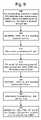
- FIG. 9depicts a via first, trench second process for forming a 3-D integrated circuit.
- FIGS. 10-16depict a trench first, via second fabrication process.
- FIG. 10depicts a layered structure for forming a 3-D integrated circuit.
- FIG. 11depicts the layered structure of FIG. 10 after patterning a trench in an oxide layer.
- FIG. 12depicts the layered structure of FIG. 11 after stripping and cleaning the AC layer.
- FIG. 13depicts the layered structure of FIG. 12 after providing AC, DARC, BARC and PR layers.
- FIG. 14depicts the layered structure of FIG. 13 after patterning a via in the oxide layer.
- FIG. 15depicts the layered structure of FIG. 14 after stripping and cleaning the AC.
- FIG. 16depicts the layered structure of FIG. 15 after applying a liner and conductive filler.
- FIG. 17depicts a trench first, via second process for forming a 3-D integrated circuit.
- FIG. 18depicts a multi-level 3-D integrated circuit structure showing a trench and via interconnect.
- FIG. 19depicts a cross-sectional view of the multi-level 3-D integrated circuit structure of FIG. 18 .
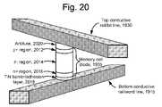
- FIG. 20depicts a memory cell in a 3-D memory device.
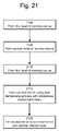
- FIG. 21depicts a process for forming a 3-D integrated circuit.
- the present inventionprovides a method for fabricating a 3-D monolithic memory device in which etching of vias and trenches is improved. A corresponding apparatus is also provided.
- a monolithic three dimensional memory array or deviceis one in which multiple memory levels are formed above a single substrate, such as a wafer, with no intervening substrates.
- the layers forming one memory levelare deposited or grown directly over the layers of an existing level or levels.
- stacked memorieshave been constructed by forming memory levels on separate substrates and adhering the memory levels atop each other, as in U.S. Pat. No. 5,915,167 to Leedy, titled “Three dimensional structure memory,” incorporated herein by reference.
- a monolithic three dimensional memory array formed above a substratecomprises at least a first memory level formed at a first height above the substrate and a second memory level formed at a second height different from the first height. Three, four, eight, or indeed any number of memory levels can be formed above the substrate in such a multilevel array.
- the etchingcan use a dual damascene process in which a BARC layer is used for patterning a second layer while protecting a first, patterned layer.
- a damascene processfeatures are formed by forming voids in a dielectric, then filling those voids with conductive or semiconductor material.
- a dual damascene processinvolves forming and filling two overlapping voids.
- approaches which are suitable for short viasmay not be sufficient in applications where deep vias are used.
- Such applicationsinclude 3-D applications, where a via, also referred to as a zia, contacts multiple levels of a 3-D device simultaneously. See, for example, V.
- the viacan be etched through multiple levels of the device in a single pass through an etcher and may have a depth of, e.g., 1.5-2.0 ⁇ m.
- a techniqueis provided herein for a dual damascene application for a 3-D zia/trench combination using an amorphous carbon hard mask.
- FIGS. 1-7depict a via first, trench second fabrication process.
- An overview of example process stepsis as follows: trench and via oxide deposition, via/zia patterning (photolithography and etch) and cleans, amorphous carbon and DARC/BARC deposition for trench patterning, trench photolithography, and trench etch and clean. Further details are provided below.
- FIG. 1depicts a layered structure for forming a 3-D integrated circuit.
- the layered structuremay be formed on a substrate, which can be any semiconducting substrate as known in the art, such as monocrystalline silicon, IV-IV compounds such as silicon-germanium or silicon-germanium-carbon, III-V compounds, II-VII compounds, epitaxial layers over such substrates, or any other semiconducting material.
- the substratemay include integrated circuits fabricated therein.
- the layered structureincludes a landing pad layer 130 , which includes a metal landing pad 135 or other conductive connection point in the circuit. Insulating material may be provided around the metal landing pad 135 in the landing pad layer 130 .
- An insulating layer 125such as SiO 2 or other oxide, is deposited above the landing pad layer 130 . Alternatively, or additionally, the insulating layer 125 can include a high-dielectric film, Si—C—O—H film, or any other suitable insulating material.
- An amorphous carbon (AC) layer 120is deposited on the insulating layer 125 and may therefore contact a top surface of the insulating layer 125 .
- the amorphous carboncan be obtained as the product “Advanced Patterning Film (APF)®”, which is available from Applied Materials Inc., Santa Clara, Calif.
- a DARC layer 115is deposited on the AC layer 120 .
- the DARC layer 115may include silicon-oxynitride, for instance.
- DARCis a deposited film produced in a PECVD reactor.
- a BARC layer 110can be used on top of the DARC layer 115 , but does not replace the properties of the DARC layer 115 in masking the amorphous carbon film stack below.
- a PR layer 105is deposited on the BARC layer 110 , when present, or on the DARC layer 115 when a BARC layer is not present.
- the PR layeris of a type which is exposed by 193 nm (deep ultraviolet) light.
- the photoresistis shown after being patterned.
- a pattern of an attenuated phase shift photomaskis transferred to the photoresist layer 105 by selectively exposing the photoresist layer to UV light and removing the exposed portion of the photoresist using a developer.
- Etching of the layered structureinvolves three different etch chemistries, namely one for etching the BARC and DARC layer, one for etching the AC layer and one for etching the oxide.
- the BARC and DARC layersare etched using the PR layer as a mask.
- the AC layeris etched mainly using the DARC layer as a hard mask.
- the oxide layeris etched essentially using the AC layer as a hard mask.
- the stacksWhen the wafer is first placed in the etcher, the stacks appear as in FIG. 1 . When the wafer is removed from the etcher, the stacks appear as in FIG. 2 . Note that the figures are not to scale. Additionally, in some cases, the step for going from the configuration of FIG. 3 to that of FIG. 4 , described further below, is also integrated into the same etch process. In the etch chamber, the BARC, DARC, AC and oxide etches and, in some cases, plasma strip of AC, occur sequentially. For example, at the end of DARC etch, there may be some PR and BARC or BARC but no PR, on the wafer. Typically, the PR/BARC is used up sometime during the AC etch.
- each layerdepends on the thickness underlying layer or layers which are being etched, and the requirements of the process architecture.
- the PR layeris about 1,000-5,000 ⁇ thick
- the BARC layeris about 200-2,000 ⁇ thick
- the DARC layeris about 200-800 ⁇ thick.
- the AC layermay be about 4,000-8,000 ⁇ thick to etch a 1-2 ⁇ m deep via in the oxide layer.
- amorphous carboncan provide an effective, easily etched, and easily removable hard mask with high selectivity to silicon, oxide, and tungsten.
- the layered structure of FIG. 1may already have other components fabricated therein, such as memory cells, word lines and bit lines, when the via and trench are formed.
- FIG. 2depicts the layered structure of FIG. 1 after patterning a via 205 in an oxide layer 125 using etching as described above.
- the viagenerally extends down to the metal landing pad 135 for subsequently forming a conductive connection to the metal landing pad.
- the viacan have a depth which is greater than about 0.5-1 ⁇ m or about 1-2 ⁇ m or more, for instance.
- the viamay be about 0.065 ⁇ m wide for a device in which a minimum feature size is 45 nm in the example implementation. Other implementations are possible as well.
- FIG. 3depicts the layered structure of FIG. 2 after stripping and cleaning the AC layer.
- a plasma stripmay be used. Having formed the via 205 , the process continues to form a trench, as discussed next.
- FIG. 4depicts the layered structure of FIG. 3 after applying AC, DARC, BARC and PR layers.
- amorphous carbonis deposited to fill in the via. Due to the narrowness and depth of the via, the amorphous carbon may not uniformly fill the via, in which case a void 425 may be formed. However, the void is not problematic as long as there is sufficient AC in the via to protect the via in the subsequent trench etch.
- the deposited amorphous carbonalso forms a layer 420 above the oxide 125 .
- a DARC layer 415is deposited on the AC layer 420 , a BARC layer 410 is optionally deposited on the DARC layer 415 , and a PR layer 405 is deposited on the BARC layer 410 , if present, or on the DARC layer 415 if the BARC layer is not present.
- the PR layer 405may subsequently be patterned to form an opening which is transferred by etching to form a trench in the oxide.
- the PR layeris about 1,000-2,000 ⁇ thick
- the BARC layeris about 200-1,000 ⁇ thick
- the DARC layeris about 200-600 ⁇ thick.
- the AC layermay be about 1,500-3,000 ⁇ thick to etch a 2,000-5,000 ⁇ deep trench in the oxide layer.
- FIG. 5depicts the layered structure of FIG. 4 after patterning a trench 505 in the oxide layer 125 when the oxide layer is etched using the AC layer 420 as a hard mask.
- the remaining portion of the AC 510 which at least partly filled in the viais also depicted.
- the trenchwill be wider than the via, although this is not required.
- the trenchextends laterally in a level of a 3-D device, such as to form word lines, bit lines, or other routing lines in the level.
- the trenchmay have a width of about 120 nm in a landing pad region, and a width of about 45 nm outside the landing pad. See also FIG. 8 .
- FIG. 6depicts the layered structure of FIG. 5 after stripping and cleaning the AC.
- a plasma stripmay be used.
- both the via 205 and trench 505have been formed.
- the viaextends generally from the bottom of the oxide layer 125 , at the top of the metal landing pad 135 , to a top of the oxide layer 125 .
- the vias in each layerwill contact one another to form a continuous via or zia in multiple levels. See also FIGS. 18 and 19 .
- FIG. 7depicts the layered structure of FIG. 6 after applying a liner and conductive filler.
- a titanium nitride (TiN) liner 705may be used as a glue layer for the conductive material 710 which is subsequently deposited.
- the conductive materialcan be tungsten (W).
- Wtungsten
- a copper (Cu) barrieris used when the oxide is a low k material.
- FIG. 8depicts a top view of the layered structure of FIG. 7 .
- the trench 505 and via 205are depicted in a landing pad area 850 of the device.
- the trenchis widened to allow room for the via.
- the trenchin the landing pad area 850 , the trench has a width A, e.g., 120 nm, and a length C, e.g., 200 nm.
- the viahas a width A, e.g., 65 nm, and a length B, e.g., 80 nm.
- the viahas an elongated cross section in this example. In other approaches, the via cross section can be circular.
- the trenchhas a narrow width, e.g., 45 nm, which is the smallest dimension in the device, in this example.
- the dimensions and configuration providedare examples only as many other dimensions and configurations can be used.
- FIG. 9depicts a via first, trench second process for forming a 3-D integrated circuit. Note that, in this and other flowcharts, the steps shown do not necessarily occur as discrete steps.
- Step 900includes providing insulating, AC, DARC, BARC and PR layers on a substrate (see FIG. 1 ).
- Step 905includes etching the BARC, DARC, AC and insulating layers using appropriate etch chemistries, to form one or more vias. Note that the different chemistries can be set, one after another, while the substrate remains in an etch chamber, as mentioned, so that the etch occurs as a continuous process.
- Step 910includes cleaning and stripping of the remaining AC layer (see FIG. 3 ).
- Step 915includes filling the via with AC and providing a new AC layer above the insulating layer.
- the stepfurther includes providing new DARC, BARC and PR layers above the new AC layer (see FIG. 4 ).
- Step 920includes etching the BARC, DARC, AC and insulating layers using appropriate etch chemistries to form a trench (see FIG. 5 ).
- the trenchis aligned with the via, and the via extends below the trench.
- Step 925includes cleaning and stripping of the remaining AC layer and the AC in the via (see FIG. 6 ).
- Step 930includes adding a titanium nitride liner, overfilling the trench and via with a conductive material such as tungsten, and performing chemical mechanical polishing to planarize the device (see FIG. 7 ).
- FIGS. 10-16depict a trench first, via second fabrication process.
- FIG. 10depicts a layered structure for forming a 3-D integrated circuit.
- the structureis analogous to that provided in FIG. 1 , and includes a landing pad layer 1030 , which includes a metal landing pad 1035 or other conductive connection point in the circuit, an insulating layer 1025 , such as SiO 2 or other oxide, an AC layer 1020 , a DARC layer 1015 , an optional BARC layer 1010 , and a PR layer 1005 .
- etching of the structure in FIG. 10may occur using different etch chemistries, but in a single continuous process.
- the stacksappear as in FIG. 10 .
- the stacksappear as in FIG. 11 .
- the step for going from the configuration of FIG. 11 to that of FIG. 12is also integrated into the same etch process.
- the PR layeris about 1,000-2,000 ⁇ thick
- the BARC layeris about 200-1,000 ⁇ thick
- the DARC layeris about 200-600 ⁇ thick.
- the AC layermay be about 1,500-3,000 ⁇ thick to etch a 2,000-5,000 ⁇ deep trench in the oxide layer.
- FIG. 11depicts the layered structure of FIG. 10 after patterning a trench 1105 in an oxide layer 1025 using etching as described above.
- the trenchgenerally is wider and shallower than a via.
- FIG. 12depicts the layered structure of FIG. 11 after stripping and cleaning the AC layer.
- a plasma stripmay be used. Having formed the trench 1105 , the process continues to form a via, as discussed next.
- FIG. 13depicts the layered structure of FIG. 12 after applying AC, DARC, BARC and PR layers.
- amorphous carbonis deposited to fill in the trench. Due to the narrowness of the trench, the amorphous carbon may not uniformly fill the trench, in which case a void 1325 may be formed. However, the void is not problematic as long as there is sufficient AC in the trench to protect the trench in the subsequent via etch.
- the deposited amorphous carbonalso forms a layer 1320 above the oxide 1025 .
- a DARC layer 1315is deposited on the AC layer 1320 , a BARC layer 1310 is optionally deposited on the DARC layer 1315 , and a PR layer 1305 is deposited on the BARC layer 1310 , if present, or on the DARC layer 1315 if the BARC layer is not present.
- the PR layer 1305may subsequently be patterned to form an opening which is transferred by etching to form a via in the oxide.
- the PR layeris about 1,000-5,000 ⁇ thick
- the BARC layeris about 200-2,000 ⁇ thick
- the DARC layeris about 200-800 ⁇ thick.
- the AC layermay be about 4,000-8,000 ⁇ thick to etch a 1-2 ⁇ m deep via in the oxide layer.
- FIG. 14depicts the layered structure of FIG. 13 after patterning a via 1405 in the oxide layer 1025 when the oxide layer is etched using the AC layer 1320 as a hard mask. The remaining portion of the AC 1310 which at least partly filled in the trench is also depicted.
- FIG. 15depicts the layered structure of FIG. 14 after stripping and cleaning the AC.
- a plasma stripmay be used.
- both the via 1405 and trench 1105have been formed.
- the viaextends generally from the bottom of the oxide layer 1025 , at the top of the metal landing pad 1035 , to a top of the oxide layer 125 .
- the vias in each layerwill contact one another to form a continuous via or zia in multiple levels. See also FIGS. 18 and 19 .
- FIG. 16depicts the layered structure of FIG. 15 after applying a liner and conductive filler.
- a titanium nitride (TiN) liner 1605may be used as a glue layer for the conductive material 1610 which is subsequently deposited.
- the conductive materialcan be tungsten (W).
- Wtungsten
- a copper (Cu) barrieris used when the oxide is a low k material.
- FIG. 17depicts a trench first, via second process for forming a 3-D integrated circuit.
- Step 1700includes providing insulating, AC, DARC, BARC and PR layers on a substrate (see FIG. 10 ).
- Step 1705includes etching the BARC, DARC, AC and insulating layers using appropriate etch chemistries, to form on or more trenches. Note that the different chemistries can be set, one after another, while the substrate remains in an etch chamber, as mentioned, so that the etch occurs as a continuous process.
- Step 1710includes cleaning and stripping of the remaining AC layer (see FIG. 12 ).
- Step 1715includes filling the trench with AC and providing a new AC layer above the insulating layer.
- the stepfurther includes providing new DARC, BARC and PR layers above the new AC layer (see FIG. 13 ).
- Step 1720includes etching the BARC, DARC, AC and insulating layers using appropriate etch chemistries to form a via (see FIG. 14 ).
- Step 1725includes cleaning and stripping of the remaining AC layer and the AC in the trench (see FIG. 15 ).
- Step 1730includes adding a titanium nitride liner, overfilling the trench and via with a conductive material such as tungsten, and performing chemical mechanical polishing to planarize the device (see FIG. 16 ).
- FIG. 18depicts a multi-level 3-D integrated circuit structure showing a trench and via interconnect.
- the layered semiconductor structure with the trench and via formed thereincan be formed to interconnect multiple levels in a 3-D device.
- the via and trenchare formed, and conductive material is provided in the via/trench.
- the conductive materialforms a continuous conductive path through the levels to provide a vertical conductive interconnect in the device.
- An example multi-level deviceincludes three levels, L 0 , L 1 and L 2 .
- An example via 1820at its bottom, connects to a respective metal pad 1805 in a landing pad layer 1800 .
- the trench 1840 at the top of the via 1820extends laterally in one of the levels of the device, L 2 , to provide a word line, bit line or other routing line.
- the oxide 1830 , liner 1850 and conductive filler 1860are also depicted. Appropriate control circuits of the multi-level device are used to provide voltages to the via and trench via the metal pad 1805 .
- FIG. 19depicts a cross-sectional view of the multi-level 3-D integrated circuit structure of FIG. 18 .
- the cross-sectiondepicts the metal pad 1805 , via 1820 , trench 1840 , liner 1850 , conductive filler 1860 and levels L 0 , L 1 and L 2 of FIG. 18 .
- the via 1820has a width which increases step wise with each higher level.
- the viacontacts, or lands on, word lines at each level of the device, in this example.
- a viacould similarly contact bit lines at different levels of a device.
- the trench 1840is used to provide word lines 1905 and 1907 .
- the viawhich includes the liner 1850 and conductive filler 1860 , lands on word lines 1910 and 1912 in the L 1 level of the device, and on word lines 1915 and 1917 in the L 0 level of the device.
- the word linesextend on both sides of the via 1820 .
- the word linesmay extend from only one side of the via 1820 .
- the word linesare conductive rails which contact bottom portions of memory cells, such as example cells 1925 , 1935 , 1945 and 1955 .
- bit lines (BLs)can be formed as conductive rails which communicate with top portions of the memory cells, such as example bit lines 1920 , 1930 , 1940 and 1950 which communicate with cells 1925 , 1935 , 1945 and 1955 , respectively. Further details regarding operation of the memory cells are discussed next.
- FIG. 20depicts a memory cell in a 3-D memory device.
- U.S. Pat. No. 6,952,030discloses an example configuration of the memory cell 1935 .
- the memory cellincludes a vertically oriented junction diode and a dielectric rupture antifuse interposed between top and bottom conductors.
- a vertically oriented junction diode 1935includes a heavily doped semiconductor layer 2012 of a first conductivity type (e.g., p+ type), a layer 2014 which is undoped or lightly doped semiconductor material, and a heavily doped semiconductor layer 2016 of a second conductivity type (e.g., n+ type).
- the semiconductor material of diode 1935can be, e.g., silicon, germanium, or an alloy of silicon and/or germanium.
- Diode 1935 and dielectric rupture antifuse 2020are arranged in series between a bottom conductor/word line 1915 and a top conductor/bit line 1930 , which may be formed of a metal such as tungsten.
- the conductorscan be in the form of rails or other elongated members which extend parallel to one another in a given level and transverse to one another in alternating levels.
- a titanium nitride adhesion and barrier layer 2018can also be provided between the diode 1935 and the bottom conductive rail 1915 .
- the diode 1935can be a junction diode, which is a semiconductor device with the property of non-ohmic conduction, having two terminal electrodes, and made of semiconducting material which is p-type at one electrode and n-type at the other.
- Examplesinclude p-n diodes and n-p diodes, which have p-type semiconductor material and n-type semiconductor material in contact, such as Zener diodes, and p-i-n diodes, in which intrinsic (undoped) semiconductor material is interposed between p-type semiconductor material and n-type semiconductor material.
- the heavily doped n-type silicon layer 2016is provided and doped in situ, followed by the layer 2014 of intrinsic or lightly doped silicon.
- Silicon regions 2016 and 2014can be amorphous as deposited, and crystallized later to polycrystalline silicon, also referred to as polysilicon.
- the p+ region 2012can be formed after the silicon is patterned and etched into pillars.
- ion implantation of a p-type dopantfor example boron or BF 2
- the polarity of the diodecould be reversed, or the semiconductor may be germanium, a silicon-germanium alloy, or some other material.
- the diode 1935acts as an open circuit when a read voltage is applied between the top conductor 1930 and the bottom conductor 1915 .
- the antifuse 2020impedes current flow, and in most embodiments the polycrystalline semiconductor material of diode 1935 is formed in a relatively high-resistivity state.
- Application of a programming voltage between the top conductor 1930 and the bottom conductor 1915causes dielectric breakdown of the antifuse material, permanently forming a conductive path through the antifuse 2020 .
- the semiconductor material of diode 1935is altered as well, changing it to a lower-resistivity state. After programming, a readily detectable current flows between the top conductor 1930 and the bottom conductor 1915 upon application of a read voltage.
- a programmed cellcan be distinguished from an unprogrammed cell.
- the cellis binary. For example, a logical one value can be assigned when no current flows, and a logical zero value can be assigned when current flows.
- Various other memory cell configurationsare possible.
- FIG. 21depicts a process for forming a 3-D integrated circuit.
- three levelsare formed.
- the processcan be adapted to form any number of levels.
- Steps 2100 , 2105 and 2110include forming first, second and third levels of the memory device, one after another. For each level, various steps for forming the memory cells, word lines and bit lines can be performed.
- Step 2115includes forming an overlapping via and trench using a dual damascene process with amorphous carbon hard mask.
- Step 2120includes filling the via and trench with conductive material.
Landscapes
- Engineering & Computer Science (AREA)
- Physics & Mathematics (AREA)
- Condensed Matter Physics & Semiconductors (AREA)
- General Physics & Mathematics (AREA)
- Manufacturing & Machinery (AREA)
- Computer Hardware Design (AREA)
- Microelectronics & Electronic Packaging (AREA)
- Power Engineering (AREA)
- Internal Circuitry In Semiconductor Integrated Circuit Devices (AREA)
Abstract
Description
- 1. Field of the Invention
- The present invention relates to fabricating a 3-D integrated circuit.
- 2. Description of the Related Art
- Due to the high cost of silicon real estate and the need to create ever smaller memory devices, monolithic 3-D memory devices have become increasingly popular. Such devices can include multiple levels of interconnected memory cells. Examples of this technology can be found in U.S. 2005/0098800, titled “Nonvolatile memory cell comprising a reduced height vertical diode,” published May 12, 2005, and U.S. Pat. No. 6,952,030, titled “High-density three-dimensional memory cell”, issued Oct. 4, 2005, both of which are incorporated herein by reference. In such devices, the memory cells can be formed as diodes in polysilicon layers, while conductive rails which interconnect the memory cells can be formed by etching oxide layers and depositing a conductive material. However, various challenges are encountered in forming interconnects between the layers of such memory devices and other 3-D integrated circuits. In particular, as 3-D monolithic integrated circuits push minimum feature sizes and etch and fill aspect ratios to the limit, conventional fabrication techniques have been found to be inadequate. For example, etching of relatively deep vias and trenches between layers can be problematic.
- The present invention addresses the above and other issues by providing a method for fabricating a 3-D monolithic memory device in which etching of vias and trenches is improved.
- In one embodiment, a method for fabricating a 3-D monolithic memory device includes first patterning of a first insulating layer to form a trench therein using a first amorphous carbon hard mask, applying amorphous carbon to fill in at least a portion of the trench and to provide an amorphous carbon layer above the first insulating layer, second patterning of the first insulating layer, using a second amorphous carbon hard mask formed from the amorphous carbon layer, to form a via in the first insulating layer which is aligned with the trench and extends below the trench, and providing a conductive material in the trench and via.
- In another embodiment, a method for fabricating a 3-D monolithic memory device includes first patterning of a first insulating layer to form a via therein using a first amorphous carbon hard mask, applying amorphous carbon to fill in at least a portion of the via and to provide an amorphous carbon layer above the first insulating layer, second patterning of the first insulating layer, using at least the amorphous carbon layer as a second amorphous carbon hard mask, to form a trench in the first insulating layer aligned with the via, the via extends below the trench, and providing a conductive material in the trench and via.
- In another embodiment, a method for fabricating a 3-D monolithic memory device includes forming conductive interconnects in the memory device, including at least a first interconnect in a first level and a second interconnect in a second level, the first and second interconnects each include an associated via and trench which are formed by a dual damascene process in which at least one of the via and trench is patterned using an associated amorphous carbon hard mask, a conductive material is provided in the via and trench, and the conductive material in the via and trench of the first interconnect is electrically coupled to the conductive material in the via and trench of the second interconnect.
FIGS. 1-7 depict a via first, trench second fabrication process.FIG. 1 depicts a layered structure for forming a 3-D integrated circuit.FIG. 2 depicts the layered structure ofFIG. 2 after patterning a via in an oxide layer.FIG. 3 depicts the layered structure ofFIG. 2 after stripping and cleaning an AC layer.FIG. 4 depicts the layered structure ofFIG. 3 after providing AC, DARC, BARC and PR layers.FIG. 5 depicts the layered structure ofFIG. 4 after patterning a trench in the oxide layer.FIG. 6 depicts the layered structure ofFIG. 5 after stripping and cleaning the AC.FIG. 7 depicts the layered structure ofFIG. 6 after applying a liner and conductive filler.FIG. 8 depicts a top view of the layered structure ofFIG. 7 .FIG. 9 depicts a via first, trench second process for forming a 3-D integrated circuit.FIGS. 10-16 depict a trench first, via second fabrication process.FIG. 10 depicts a layered structure for forming a 3-D integrated circuit.FIG. 11 depicts the layered structure ofFIG. 10 after patterning a trench in an oxide layer.FIG. 12 depicts the layered structure ofFIG. 11 after stripping and cleaning the AC layer.FIG. 13 depicts the layered structure ofFIG. 12 after providing AC, DARC, BARC and PR layers.FIG. 14 depicts the layered structure ofFIG. 13 after patterning a via in the oxide layer.FIG. 15 depicts the layered structure ofFIG. 14 after stripping and cleaning the AC.FIG. 16 depicts the layered structure ofFIG. 15 after applying a liner and conductive filler.FIG. 17 depicts a trench first, via second process for forming a 3-D integrated circuit.FIG. 18 depicts a multi-level 3-D integrated circuit structure showing a trench and via interconnect.FIG. 19 depicts a cross-sectional view of the multi-level 3-D integrated circuit structure ofFIG. 18 .FIG. 20 depicts a memory cell in a 3-D memory device.FIG. 21 depicts a process for forming a 3-D integrated circuit.- The present invention provides a method for fabricating a 3-D monolithic memory device in which etching of vias and trenches is improved. A corresponding apparatus is also provided.
- The following acronyms and abbreviations are used:
- AC—amorphous carbon;
- BARC—bottom antireflective coating, available from Brewer Science, Rolla, Mo.
- DARC—dielectric antireflective coating; and
- PR—photoresist.
- As mentioned at the outset, etching of relatively deep vias and trenches between layers in a 3-D monolithic memory device can be problematic. A monolithic three dimensional memory array or device is one in which multiple memory levels are formed above a single substrate, such as a wafer, with no intervening substrates. The layers forming one memory level are deposited or grown directly over the layers of an existing level or levels. In contrast, stacked memories have been constructed by forming memory levels on separate substrates and adhering the memory levels atop each other, as in U.S. Pat. No. 5,915,167 to Leedy, titled “Three dimensional structure memory,” incorporated herein by reference. The substrates may be thinned or removed from the memory levels before bonding, but as the memory levels are initially formed over separate substrates, such memories are not true monolithic three dimensional memory arrays. A monolithic three dimensional memory array formed above a substrate comprises at least a first memory level formed at a first height above the substrate and a second memory level formed at a second height different from the first height. Three, four, eight, or indeed any number of memory levels can be formed above the substrate in such a multilevel array.
- For short vias and trenches, e.g., less than about 0.5 μm, the etching can use a dual damascene process in which a BARC layer is used for patterning a second layer while protecting a first, patterned layer. In a damascene process, features are formed by forming voids in a dielectric, then filling those voids with conductive or semiconductor material. A dual damascene process involves forming and filling two overlapping voids. However, approaches which are suitable for short vias may not be sufficient in applications where deep vias are used. Such applications include 3-D applications, where a via, also referred to as a zia, contacts multiple levels of a 3-D device simultaneously. See, for example, V. Dunton et al., “Zias: Vertical wires in 3-D memory devices,” Matrix Semiconductor, 2005 VMIC Conference, Oct. 4-6, 2005, incorporated herein by reference. The via can be etched through multiple levels of the device in a single pass through an etcher and may have a depth of, e.g., 1.5-2.0 μm. A technique is provided herein for a dual damascene application for a 3-D zia/trench combination using an amorphous carbon hard mask.
FIGS. 1-7 depict a via first, trench second fabrication process. An overview of example process steps is as follows: trench and via oxide deposition, via/zia patterning (photolithography and etch) and cleans, amorphous carbon and DARC/BARC deposition for trench patterning, trench photolithography, and trench etch and clean. Further details are provided below.FIG. 1 depicts a layered structure for forming a 3-D integrated circuit. The layered structure may be formed on a substrate, which can be any semiconducting substrate as known in the art, such as monocrystalline silicon, IV-IV compounds such as silicon-germanium or silicon-germanium-carbon, III-V compounds, II-VII compounds, epitaxial layers over such substrates, or any other semiconducting material. The substrate may include integrated circuits fabricated therein.- The layered structure includes a
landing pad layer 130, which includes ametal landing pad 135 or other conductive connection point in the circuit. Insulating material may be provided around themetal landing pad 135 in thelanding pad layer 130. An insulating layer125, such as SiO2or other oxide, is deposited above thelanding pad layer 130. Alternatively, or additionally, the insulating layer125 can include a high-dielectric film, Si—C—O—H film, or any other suitable insulating material. An amorphous carbon (AC)layer 120 is deposited on the insulating layer125 and may therefore contact a top surface of the insulating layer125. The amorphous carbon can be obtained as the product “Advanced Patterning Film (APF)®”, which is available from Applied Materials Inc., Santa Clara, Calif. A DARC layer115 is deposited on theAC layer 120. The DARC layer115 may include silicon-oxynitride, for instance. DARC is a deposited film produced in a PECVD reactor. Optionally, a BARC layer110 can be used on top of the DARC layer115, but does not replace the properties of the DARC layer115 in masking the amorphous carbon film stack below. APR layer 105 is deposited on the BARC layer110, when present, or on the DARC layer115 when a BARC layer is not present. In one possible implementation, the PR layer is of a type which is exposed by 193 nm (deep ultraviolet) light. The photoresist is shown after being patterned. In one possible approach, a pattern of an attenuated phase shift photomask is transferred to thephotoresist layer 105 by selectively exposing the photoresist layer to UV light and removing the exposed portion of the photoresist using a developer. - Etching of the layered structure involves three different etch chemistries, namely one for etching the BARC and DARC layer, one for etching the AC layer and one for etching the oxide. In the first etch, the BARC and DARC layers are etched using the PR layer as a mask. In the second etch, the AC layer is etched mainly using the DARC layer as a hard mask. In the third etch, the oxide layer is etched essentially using the AC layer as a hard mask. Although different etch chemistries are used, the etch can be a single, continuous process in which a wafer with photo patterning is placed into an etcher and all the films are etched in a single pass. When the wafer is first placed in the etcher, the stacks appear as in
FIG. 1 . When the wafer is removed from the etcher, the stacks appear as inFIG. 2 . Note that the figures are not to scale. Additionally, in some cases, the step for going from the configuration ofFIG. 3 to that ofFIG. 4 , described further below, is also integrated into the same etch process. In the etch chamber, the BARC, DARC, AC and oxide etches and, in some cases, plasma strip of AC, occur sequentially. For example, at the end of DARC etch, there may be some PR and BARC or BARC but no PR, on the wafer. Typically, the PR/BARC is used up sometime during the AC etch. - Further, the required thickness of each layer depends on the thickness underlying layer or layers which are being etched, and the requirements of the process architecture. For the via etch, in an example implementation, the PR layer is about 1,000-5,000 Å thick, the BARC layer is about 200-2,000 Å thick, and the DARC layer is about 200-800 Å thick. The AC layer may be about 4,000-8,000 Å thick to etch a 1-2 μm deep via in the oxide layer. Generally, amorphous carbon can provide an effective, easily etched, and easily removable hard mask with high selectivity to silicon, oxide, and tungsten.
- Note that the layered structure of
FIG. 1 may already have other components fabricated therein, such as memory cells, word lines and bit lines, when the via and trench are formed. FIG. 2 depicts the layered structure ofFIG. 1 after patterning a via205 in an oxide layer125 using etching as described above. The via generally extends down to themetal landing pad 135 for subsequently forming a conductive connection to the metal landing pad. In an example implementation, the via can have a depth which is greater than about 0.5-1 μm or about 1-2 μm or more, for instance. The via may be about 0.065 μm wide for a device in which a minimum feature size is 45 nm in the example implementation. Other implementations are possible as well.FIG. 3 depicts the layered structure ofFIG. 2 after stripping and cleaning the AC layer. For example, a plasma strip may be used. Having formed the via205, the process continues to form a trench, as discussed next.FIG. 4 depicts the layered structure ofFIG. 3 after applying AC, DARC, BARC and PR layers. First, amorphous carbon is deposited to fill in the via. Due to the narrowness and depth of the via, the amorphous carbon may not uniformly fill the via, in which case a void425 may be formed. However, the void is not problematic as long as there is sufficient AC in the via to protect the via in the subsequent trench etch. The deposited amorphous carbon also forms alayer 420 above the oxide125. Subsequently, aDARC layer 415 is deposited on theAC layer 420, aBARC layer 410 is optionally deposited on theDARC layer 415, and aPR layer 405 is deposited on theBARC layer 410, if present, or on theDARC layer 415 if the BARC layer is not present. ThePR layer 405 may subsequently be patterned to form an opening which is transferred by etching to form a trench in the oxide. For the trench etch, in an example implementation, the PR layer is about 1,000-2,000 Å thick, the BARC layer is about 200-1,000 Å thick, and the DARC layer is about 200-600 Å thick. The AC layer may be about 1,500-3,000 Å thick to etch a 2,000-5,000 Å deep trench in the oxide layer.FIG. 5 depicts the layered structure ofFIG. 4 after patterning atrench 505 in the oxide layer125 when the oxide layer is etched using theAC layer 420 as a hard mask. The remaining portion of the AC510 which at least partly filled in the via is also depicted. Generally, the trench will be wider than the via, although this is not required. The trench extends laterally in a level of a 3-D device, such as to form word lines, bit lines, or other routing lines in the level. The trench may have a width of about 120 nm in a landing pad region, and a width of about 45 nm outside the landing pad. See alsoFIG. 8 .FIG. 6 depicts the layered structure ofFIG. 5 after stripping and cleaning the AC. As mentioned previously, a plasma strip may be used. At this point, both the via205 andtrench 505 have been formed. The via extends generally from the bottom of the oxide layer125, at the top of themetal landing pad 135, to a top of the oxide layer125. When subsequent levels are formed in a 3-D device, the vias in each layer will contact one another to form a continuous via or zia in multiple levels. See alsoFIGS. 18 and 19 .FIG. 7 depicts the layered structure ofFIG. 6 after applying a liner and conductive filler. A titanium nitride (TiN)liner 705 may be used as a glue layer for theconductive material 710 which is subsequently deposited. For example, the conductive material can be tungsten (W). Generally, any suitable conductor that can fill in the trench and via, and withstand high processing temperatures, such as 750 C, can be used. In another possible approach, a copper (Cu) barrier is used when the oxide is a low k material.FIG. 8 depicts a top view of the layered structure ofFIG. 7 . Thetrench 505 and via205 are depicted in alanding pad area 850 of the device. Here, the trench is widened to allow room for the via. In an example implementation, in thelanding pad area 850, the trench has a width A, e.g., 120 nm, and a length C, e.g., 200 nm. The via has a width A, e.g., 65 nm, and a length B, e.g., 80 nm. The via has an elongated cross section in this example. In other approaches, the via cross section can be circular. Outside thelanding pad area 850, the trench has a narrow width, e.g., 45 nm, which is the smallest dimension in the device, in this example. The dimensions and configuration provided are examples only as many other dimensions and configurations can be used. An example sequence for carrying out the above-described process is summarized below.FIG. 9 depicts a via first, trench second process for forming a 3-D integrated circuit. Note that, in this and other flowcharts, the steps shown do not necessarily occur as discrete steps. Step900 includes providing insulating, AC, DARC, BARC and PR layers on a substrate (seeFIG. 1 ). Step905 includes etching the BARC, DARC, AC and insulating layers using appropriate etch chemistries, to form one or more vias. Note that the different chemistries can be set, one after another, while the substrate remains in an etch chamber, as mentioned, so that the etch occurs as a continuous process. Step910 includes cleaning and stripping of the remaining AC layer (seeFIG. 3 ). Step915 includes filling the via with AC and providing a new AC layer above the insulating layer. The step further includes providing new DARC, BARC and PR layers above the new AC layer (seeFIG. 4 ). Step920 includes etching the BARC, DARC, AC and insulating layers using appropriate etch chemistries to form a trench (seeFIG. 5 ). The trench is aligned with the via, and the via extends below the trench. Step925 includes cleaning and stripping of the remaining AC layer and the AC in the via (seeFIG. 6 ). Step930 includes adding a titanium nitride liner, overfilling the trench and via with a conductive material such as tungsten, and performing chemical mechanical polishing to planarize the device (seeFIG. 7 ).- As an alternative to the via first option discussed, a trench first process may be used, as discussed next.
FIGS. 10-16 depict a trench first, via second fabrication process. FIG. 10 depicts a layered structure for forming a 3-D integrated circuit. The structure is analogous to that provided inFIG. 1 , and includes alanding pad layer 1030, which includes ametal landing pad 1035 or other conductive connection point in the circuit, an insulating layer1025, such as SiO2or other oxide, anAC layer 1020, aDARC layer 1015, anoptional BARC layer 1010, and aPR layer 1005.- As discussed, etching of the structure in
FIG. 10 may occur using different etch chemistries, but in a single continuous process. When the wafer is first placed in the etcher, the stacks appear as inFIG. 10 . When the wafer is removed from the etcher, the stacks appear as inFIG. 11 . Again, note that the figures are not to scale. Additionally, in some cases, the step for going from the configuration ofFIG. 11 to that ofFIG. 12 , discussed further below, is also integrated into the same etch process. For the trench etch, in an example implementation, the PR layer is about 1,000-2,000 Å thick, the BARC layer is about 200-1,000 Å thick, and the DARC layer is about 200-600 Å thick. The AC layer may be about 1,500-3,000 Å thick to etch a 2,000-5,000 Å deep trench in the oxide layer. FIG. 11 depicts the layered structure ofFIG. 10 after patterning atrench 1105 in an oxide layer1025 using etching as described above. The trench generally is wider and shallower than a via.FIG. 12 depicts the layered structure ofFIG. 11 after stripping and cleaning the AC layer. A plasma strip may be used. Having formed thetrench 1105, the process continues to form a via, as discussed next.FIG. 13 depicts the layered structure ofFIG. 12 after applying AC, DARC, BARC and PR layers. First, amorphous carbon is deposited to fill in the trench. Due to the narrowness of the trench, the amorphous carbon may not uniformly fill the trench, in which case a void1325 may be formed. However, the void is not problematic as long as there is sufficient AC in the trench to protect the trench in the subsequent via etch. The deposited amorphous carbon also forms alayer 1320 above the oxide1025. Subsequently, aDARC layer 1315 is deposited on theAC layer 1320, aBARC layer 1310 is optionally deposited on theDARC layer 1315, and aPR layer 1305 is deposited on theBARC layer 1310, if present, or on theDARC layer 1315 if the BARC layer is not present. ThePR layer 1305 may subsequently be patterned to form an opening which is transferred by etching to form a via in the oxide. For the via etch, in an example implementation, the PR layer is about 1,000-5,000 Å thick, the BARC layer is about 200-2,000 Å thick, the DARC layer is about 200-800 Å thick. The AC layer may be about 4,000-8,000 Å thick to etch a 1-2 μm deep via in the oxide layer.FIG. 14 depicts the layered structure ofFIG. 13 after patterning a via1405 in the oxide layer1025 when the oxide layer is etched using theAC layer 1320 as a hard mask. The remaining portion of theAC 1310 which at least partly filled in the trench is also depicted.FIG. 15 depicts the layered structure ofFIG. 14 after stripping and cleaning the AC. As mentioned previously, a plasma strip may be used. At this point, both the via1405 andtrench 1105 have been formed. The via extends generally from the bottom of the oxide layer1025, at the top of themetal landing pad 1035, to a top of the oxide layer125. When subsequent levels are formed in a 3-D device, the vias in each layer will contact one another to form a continuous via or zia in multiple levels. See alsoFIGS. 18 and 19 .FIG. 16 depicts the layered structure ofFIG. 15 after applying a liner and conductive filler. A titanium nitride (TiN)liner 1605 may be used as a glue layer for theconductive material 1610 which is subsequently deposited. For example, the conductive material can be tungsten (W). Generally, any suitable conductor that can fill in the trench and via, and withstand high processing temperatures, such as 750 C, can be used. In another possible approach, a copper (Cu) barrier is used when the oxide is a low k material.FIG. 17 depicts a trench first, via second process for forming a 3-D integrated circuit.Step 1700 includes providing insulating, AC, DARC, BARC and PR layers on a substrate (seeFIG. 10 ).Step 1705 includes etching the BARC, DARC, AC and insulating layers using appropriate etch chemistries, to form on or more trenches. Note that the different chemistries can be set, one after another, while the substrate remains in an etch chamber, as mentioned, so that the etch occurs as a continuous process.Step 1710 includes cleaning and stripping of the remaining AC layer (seeFIG. 12 ).Step 1715 includes filling the trench with AC and providing a new AC layer above the insulating layer. The step further includes providing new DARC, BARC and PR layers above the new AC layer (seeFIG. 13 ).Step 1720 includes etching the BARC, DARC, AC and insulating layers using appropriate etch chemistries to form a via (seeFIG. 14 ).Step 1725 includes cleaning and stripping of the remaining AC layer and the AC in the trench (seeFIG. 15 ).Step 1730 includes adding a titanium nitride liner, overfilling the trench and via with a conductive material such as tungsten, and performing chemical mechanical polishing to planarize the device (seeFIG. 16 ).FIG. 18 depicts a multi-level 3-D integrated circuit structure showing a trench and via interconnect. As mentioned, the layered semiconductor structure with the trench and via formed therein, such as provided inFIGS. 7 and 16 , can be formed to interconnect multiple levels in a 3-D device. After the levels are formed, the via and trench are formed, and conductive material is provided in the via/trench. The conductive material forms a continuous conductive path through the levels to provide a vertical conductive interconnect in the device.- An example multi-level device includes three levels, L0, L1 and L2. An example via1820, at its bottom, connects to a
respective metal pad 1805 in alanding pad layer 1800. Thetrench 1840 at the top of the via1820 extends laterally in one of the levels of the device, L2, to provide a word line, bit line or other routing line. Theoxide 1830,liner 1850 andconductive filler 1860, are also depicted. Appropriate control circuits of the multi-level device are used to provide voltages to the via and trench via themetal pad 1805. FIG. 19 depicts a cross-sectional view of the multi-level 3-D integrated circuit structure ofFIG. 18 . The cross-section depicts themetal pad 1805, via1820,trench 1840,liner 1850,conductive filler 1860 and levels L0, L1 and L2 ofFIG. 18 . In particular, it can be seen that the via1820 has a width which increases step wise with each higher level. Further, the via contacts, or lands on, word lines at each level of the device, in this example. A via could similarly contact bit lines at different levels of a device. At the top of the via, thetrench 1840 is used to provideword lines liner 1850 andconductive filler 1860, lands onword lines word lines example cells example bit lines cells FIG. 20 depicts a memory cell in a 3-D memory device. U.S. Pat. No. 6,952,030, incorporated herein by reference, discloses an example configuration of thememory cell 1935. In this case, the memory cell includes a vertically oriented junction diode and a dielectric rupture antifuse interposed between top and bottom conductors. In particular, a vertically orientedjunction diode 1935 includes a heavily doped semiconductor layer2012 of a first conductivity type (e.g., p+ type), alayer 2014 which is undoped or lightly doped semiconductor material, and a heavily dopedsemiconductor layer 2016 of a second conductivity type (e.g., n+ type). The semiconductor material ofdiode 1935 can be, e.g., silicon, germanium, or an alloy of silicon and/or germanium.Diode 1935 and dielectric rupture antifuse2020 are arranged in series between a bottom conductor/word line 1915 and a top conductor/bit line 1930, which may be formed of a metal such as tungsten. The conductors can be in the form of rails or other elongated members which extend parallel to one another in a given level and transverse to one another in alternating levels. A titanium nitride adhesion andbarrier layer 2018 can also be provided between thediode 1935 and the bottomconductive rail 1915.- The
diode 1935 can be a junction diode, which is a semiconductor device with the property of non-ohmic conduction, having two terminal electrodes, and made of semiconducting material which is p-type at one electrode and n-type at the other. Examples include p-n diodes and n-p diodes, which have p-type semiconductor material and n-type semiconductor material in contact, such as Zener diodes, and p-i-n diodes, in which intrinsic (undoped) semiconductor material is interposed between p-type semiconductor material and n-type semiconductor material. - In one possible approach, the heavily doped n-
type silicon layer 2016 is provided and doped in situ, followed by thelayer 2014 of intrinsic or lightly doped silicon.Silicon regions - In the initial state of the memory cell, the
diode 1935 acts as an open circuit when a read voltage is applied between thetop conductor 1930 and thebottom conductor 1915. The antifuse2020 impedes current flow, and in most embodiments the polycrystalline semiconductor material ofdiode 1935 is formed in a relatively high-resistivity state. Application of a programming voltage between thetop conductor 1930 and thebottom conductor 1915 causes dielectric breakdown of the antifuse material, permanently forming a conductive path through the antifuse2020. The semiconductor material ofdiode 1935 is altered as well, changing it to a lower-resistivity state. After programming, a readily detectable current flows between thetop conductor 1930 and thebottom conductor 1915 upon application of a read voltage. In this way a programmed cell can be distinguished from an unprogrammed cell. Further, the cell is binary. For example, a logical one value can be assigned when no current flows, and a logical zero value can be assigned when current flows. Various other memory cell configurations are possible. FIG. 21 depicts a process for forming a 3-D integrated circuit. In the example process, three levels are formed. However, the process can be adapted to form any number of levels.Steps Step 2115 includes forming an overlapping via and trench using a dual damascene process with amorphous carbon hard mask.Step 2120 includes filling the via and trench with conductive material.- The foregoing detailed description of the invention has been presented for purposes of illustration and description. It is not intended to be exhaustive or to limit the invention to the precise form disclosed. Many modifications and variations are possible in light of the above teaching. The described embodiments were chosen in order to best explain the principles of the invention and its practical application, to thereby enable others skilled in the art to best utilize the invention in various embodiments and with various modifications as are suited to the particular use contemplated. It is intended that the scope of the invention be defined by the claims appended hereto.
Claims (23)
Priority Applications (1)
| Application Number | Priority Date | Filing Date | Title |
|---|---|---|---|
| US11/864,759US8298931B2 (en) | 2007-09-28 | 2007-09-28 | Dual damascene with amorphous carbon for 3D deep via/trench application |
Applications Claiming Priority (1)
| Application Number | Priority Date | Filing Date | Title |
|---|---|---|---|
| US11/864,759US8298931B2 (en) | 2007-09-28 | 2007-09-28 | Dual damascene with amorphous carbon for 3D deep via/trench application |
Publications (2)
| Publication Number | Publication Date |
|---|---|
| US20090087979A1true US20090087979A1 (en) | 2009-04-02 |
| US8298931B2 US8298931B2 (en) | 2012-10-30 |
Family
ID=40508856
Family Applications (1)
| Application Number | Title | Priority Date | Filing Date |
|---|---|---|---|
| US11/864,759Expired - Fee RelatedUS8298931B2 (en) | 2007-09-28 | 2007-09-28 | Dual damascene with amorphous carbon for 3D deep via/trench application |
Country Status (1)
| Country | Link |
|---|---|
| US (1) | US8298931B2 (en) |
Cited By (130)
| Publication number | Priority date | Publication date | Assignee | Title |
|---|---|---|---|---|
| US20090311635A1 (en)* | 2008-06-16 | 2009-12-17 | Chen Hui W | Double exposure patterning with carbonaceous hardmask |
| US20110049465A1 (en)* | 2009-09-02 | 2011-03-03 | Kabushiki Kaisha Toshiba | Semiconductor integrated circuit device and method of fabricating the same |
| US20110244683A1 (en)* | 2010-04-01 | 2011-10-06 | Michiaki Sano | Fabricating Voids Using Slurry Protect Coat Before Chemical-Mechanical Polishing |
| US9287095B2 (en) | 2013-12-17 | 2016-03-15 | Applied Materials, Inc. | Semiconductor system assemblies and methods of operation |
| US9287134B2 (en) | 2014-01-17 | 2016-03-15 | Applied Materials, Inc. | Titanium oxide etch |
| US9293568B2 (en) | 2014-01-27 | 2016-03-22 | Applied Materials, Inc. | Method of fin patterning |
| US9299575B2 (en) | 2014-03-17 | 2016-03-29 | Applied Materials, Inc. | Gas-phase tungsten etch |
| US9299537B2 (en) | 2014-03-20 | 2016-03-29 | Applied Materials, Inc. | Radial waveguide systems and methods for post-match control of microwaves |
| US9305923B1 (en) | 2014-12-02 | 2016-04-05 | International Business Machines Corporation | Low resistance replacement metal gate structure |
| US9309598B2 (en) | 2014-05-28 | 2016-04-12 | Applied Materials, Inc. | Oxide and metal removal |
| US9324576B2 (en) | 2010-05-27 | 2016-04-26 | Applied Materials, Inc. | Selective etch for silicon films |
| US9343272B1 (en) | 2015-01-08 | 2016-05-17 | Applied Materials, Inc. | Self-aligned process |
| US9349605B1 (en) | 2015-08-07 | 2016-05-24 | Applied Materials, Inc. | Oxide etch selectivity systems and methods |
| US9355862B2 (en)* | 2014-09-24 | 2016-05-31 | Applied Materials, Inc. | Fluorine-based hardmask removal |
| US9355863B2 (en) | 2012-12-18 | 2016-05-31 | Applied Materials, Inc. | Non-local plasma oxide etch |
| US9355856B2 (en) | 2014-09-12 | 2016-05-31 | Applied Materials, Inc. | V trench dry etch |
| US9362130B2 (en) | 2013-03-01 | 2016-06-07 | Applied Materials, Inc. | Enhanced etching processes using remote plasma sources |
| US9368364B2 (en) | 2014-09-24 | 2016-06-14 | Applied Materials, Inc. | Silicon etch process with tunable selectivity to SiO2 and other materials |
| US9373517B2 (en) | 2012-08-02 | 2016-06-21 | Applied Materials, Inc. | Semiconductor processing with DC assisted RF power for improved control |
| US9373522B1 (en) | 2015-01-22 | 2016-06-21 | Applied Mateials, Inc. | Titanium nitride removal |
| US9378969B2 (en) | 2014-06-19 | 2016-06-28 | Applied Materials, Inc. | Low temperature gas-phase carbon removal |
| US9378978B2 (en) | 2014-07-31 | 2016-06-28 | Applied Materials, Inc. | Integrated oxide recess and floating gate fin trimming |
| US9384997B2 (en) | 2012-11-20 | 2016-07-05 | Applied Materials, Inc. | Dry-etch selectivity |
| US9385028B2 (en) | 2014-02-03 | 2016-07-05 | Applied Materials, Inc. | Air gap process |
| US9390937B2 (en) | 2012-09-20 | 2016-07-12 | Applied Materials, Inc. | Silicon-carbon-nitride selective etch |
| US9396989B2 (en) | 2014-01-27 | 2016-07-19 | Applied Materials, Inc. | Air gaps between copper lines |
| US9406523B2 (en) | 2014-06-19 | 2016-08-02 | Applied Materials, Inc. | Highly selective doped oxide removal method |
| US9412608B2 (en) | 2012-11-30 | 2016-08-09 | Applied Materials, Inc. | Dry-etch for selective tungsten removal |
| US9418858B2 (en) | 2011-10-07 | 2016-08-16 | Applied Materials, Inc. | Selective etch of silicon by way of metastable hydrogen termination |
| US9425058B2 (en) | 2014-07-24 | 2016-08-23 | Applied Materials, Inc. | Simplified litho-etch-litho-etch process |
| US9437451B2 (en) | 2012-09-18 | 2016-09-06 | Applied Materials, Inc. | Radical-component oxide etch |
| US9449845B2 (en) | 2012-12-21 | 2016-09-20 | Applied Materials, Inc. | Selective titanium nitride etching |
| US9449846B2 (en) | 2015-01-28 | 2016-09-20 | Applied Materials, Inc. | Vertical gate separation |
| US9449850B2 (en) | 2013-03-15 | 2016-09-20 | Applied Materials, Inc. | Processing systems and methods for halide scavenging |
| US9472412B2 (en) | 2013-12-02 | 2016-10-18 | Applied Materials, Inc. | Procedure for etch rate consistency |
| US9478432B2 (en) | 2014-09-25 | 2016-10-25 | Applied Materials, Inc. | Silicon oxide selective removal |
| US9496167B2 (en) | 2014-07-31 | 2016-11-15 | Applied Materials, Inc. | Integrated bit-line airgap formation and gate stack post clean |
| US9493879B2 (en) | 2013-07-12 | 2016-11-15 | Applied Materials, Inc. | Selective sputtering for pattern transfer |
| US9502258B2 (en) | 2014-12-23 | 2016-11-22 | Applied Materials, Inc. | Anisotropic gap etch |
| US9499898B2 (en) | 2014-03-03 | 2016-11-22 | Applied Materials, Inc. | Layered thin film heater and method of fabrication |
| US9520303B2 (en) | 2013-11-12 | 2016-12-13 | Applied Materials, Inc. | Aluminum selective etch |
| US9553102B2 (en) | 2014-08-19 | 2017-01-24 | Applied Materials, Inc. | Tungsten separation |
| US9576809B2 (en) | 2013-11-04 | 2017-02-21 | Applied Materials, Inc. | Etch suppression with germanium |
| US9607856B2 (en) | 2013-03-05 | 2017-03-28 | Applied Materials, Inc. | Selective titanium nitride removal |
| US9659753B2 (en) | 2014-08-07 | 2017-05-23 | Applied Materials, Inc. | Grooved insulator to reduce leakage current |
| US9691645B2 (en) | 2015-08-06 | 2017-06-27 | Applied Materials, Inc. | Bolted wafer chuck thermal management systems and methods for wafer processing systems |
| US9721789B1 (en) | 2016-10-04 | 2017-08-01 | Applied Materials, Inc. | Saving ion-damaged spacers |
| US9728437B2 (en) | 2015-02-03 | 2017-08-08 | Applied Materials, Inc. | High temperature chuck for plasma processing systems |
| US9741593B2 (en) | 2015-08-06 | 2017-08-22 | Applied Materials, Inc. | Thermal management systems and methods for wafer processing systems |
| US9768034B1 (en) | 2016-11-11 | 2017-09-19 | Applied Materials, Inc. | Removal methods for high aspect ratio structures |
| US9773648B2 (en) | 2013-08-30 | 2017-09-26 | Applied Materials, Inc. | Dual discharge modes operation for remote plasma |
| US9842744B2 (en) | 2011-03-14 | 2017-12-12 | Applied Materials, Inc. | Methods for etch of SiN films |
| US9865484B1 (en) | 2016-06-29 | 2018-01-09 | Applied Materials, Inc. | Selective etch using material modification and RF pulsing |
| US9881805B2 (en) | 2015-03-02 | 2018-01-30 | Applied Materials, Inc. | Silicon selective removal |
| US9887096B2 (en) | 2012-09-17 | 2018-02-06 | Applied Materials, Inc. | Differential silicon oxide etch |
| US9885117B2 (en) | 2014-03-31 | 2018-02-06 | Applied Materials, Inc. | Conditioned semiconductor system parts |
| US9934942B1 (en) | 2016-10-04 | 2018-04-03 | Applied Materials, Inc. | Chamber with flow-through source |
| US9947549B1 (en) | 2016-10-10 | 2018-04-17 | Applied Materials, Inc. | Cobalt-containing material removal |
| US9966240B2 (en) | 2014-10-14 | 2018-05-08 | Applied Materials, Inc. | Systems and methods for internal surface conditioning assessment in plasma processing equipment |
| US9978564B2 (en) | 2012-09-21 | 2018-05-22 | Applied Materials, Inc. | Chemical control features in wafer process equipment |
| US10026621B2 (en) | 2016-11-14 | 2018-07-17 | Applied Materials, Inc. | SiN spacer profile patterning |
| US10043674B1 (en) | 2017-08-04 | 2018-08-07 | Applied Materials, Inc. | Germanium etching systems and methods |
| US10043684B1 (en) | 2017-02-06 | 2018-08-07 | Applied Materials, Inc. | Self-limiting atomic thermal etching systems and methods |
| US10049891B1 (en) | 2017-05-31 | 2018-08-14 | Applied Materials, Inc. | Selective in situ cobalt residue removal |
| US10062575B2 (en) | 2016-09-09 | 2018-08-28 | Applied Materials, Inc. | Poly directional etch by oxidation |
| US10062587B2 (en) | 2012-07-18 | 2018-08-28 | Applied Materials, Inc. | Pedestal with multi-zone temperature control and multiple purge capabilities |
| US10062585B2 (en) | 2016-10-04 | 2018-08-28 | Applied Materials, Inc. | Oxygen compatible plasma source |
| US10062578B2 (en) | 2011-03-14 | 2018-08-28 | Applied Materials, Inc. | Methods for etch of metal and metal-oxide films |
| US10062579B2 (en) | 2016-10-07 | 2018-08-28 | Applied Materials, Inc. | Selective SiN lateral recess |
| US10128086B1 (en) | 2017-10-24 | 2018-11-13 | Applied Materials, Inc. | Silicon pretreatment for nitride removal |
| US10163696B2 (en) | 2016-11-11 | 2018-12-25 | Applied Materials, Inc. | Selective cobalt removal for bottom up gapfill |
| US10170336B1 (en) | 2017-08-04 | 2019-01-01 | Applied Materials, Inc. | Methods for anisotropic control of selective silicon removal |
| US10224210B2 (en) | 2014-12-09 | 2019-03-05 | Applied Materials, Inc. | Plasma processing system with direct outlet toroidal plasma source |
| US10242908B2 (en) | 2016-11-14 | 2019-03-26 | Applied Materials, Inc. | Airgap formation with damage-free copper |
| US10256112B1 (en) | 2017-12-08 | 2019-04-09 | Applied Materials, Inc. | Selective tungsten removal |
| US10256079B2 (en) | 2013-02-08 | 2019-04-09 | Applied Materials, Inc. | Semiconductor processing systems having multiple plasma configurations |
| US10283321B2 (en) | 2011-01-18 | 2019-05-07 | Applied Materials, Inc. | Semiconductor processing system and methods using capacitively coupled plasma |
| US10283324B1 (en) | 2017-10-24 | 2019-05-07 | Applied Materials, Inc. | Oxygen treatment for nitride etching |
| US10297458B2 (en) | 2017-08-07 | 2019-05-21 | Applied Materials, Inc. | Process window widening using coated parts in plasma etch processes |
| US10319649B2 (en) | 2017-04-11 | 2019-06-11 | Applied Materials, Inc. | Optical emission spectroscopy (OES) for remote plasma monitoring |
| US10319739B2 (en) | 2017-02-08 | 2019-06-11 | Applied Materials, Inc. | Accommodating imperfectly aligned memory holes |
| US10319600B1 (en) | 2018-03-12 | 2019-06-11 | Applied Materials, Inc. | Thermal silicon etch |
| US10354889B2 (en) | 2017-07-17 | 2019-07-16 | Applied Materials, Inc. | Non-halogen etching of silicon-containing materials |
| US10403507B2 (en) | 2017-02-03 | 2019-09-03 | Applied Materials, Inc. | Shaped etch profile with oxidation |
| US10431429B2 (en) | 2017-02-03 | 2019-10-01 | Applied Materials, Inc. | Systems and methods for radial and azimuthal control of plasma uniformity |
| US10468267B2 (en) | 2017-05-31 | 2019-11-05 | Applied Materials, Inc. | Water-free etching methods |
| US10490406B2 (en) | 2018-04-10 | 2019-11-26 | Appled Materials, Inc. | Systems and methods for material breakthrough |
| US10497573B2 (en) | 2018-03-13 | 2019-12-03 | Applied Materials, Inc. | Selective atomic layer etching of semiconductor materials |
| US10504700B2 (en) | 2015-08-27 | 2019-12-10 | Applied Materials, Inc. | Plasma etching systems and methods with secondary plasma injection |
| US10504754B2 (en) | 2016-05-19 | 2019-12-10 | Applied Materials, Inc. | Systems and methods for improved semiconductor etching and component protection |
| US10522371B2 (en) | 2016-05-19 | 2019-12-31 | Applied Materials, Inc. | Systems and methods for improved semiconductor etching and component protection |
| US10541184B2 (en) | 2017-07-11 | 2020-01-21 | Applied Materials, Inc. | Optical emission spectroscopic techniques for monitoring etching |
| US10541246B2 (en) | 2017-06-26 | 2020-01-21 | Applied Materials, Inc. | 3D flash memory cells which discourage cross-cell electrical tunneling |
| US10546729B2 (en) | 2016-10-04 | 2020-01-28 | Applied Materials, Inc. | Dual-channel showerhead with improved profile |
| US10566206B2 (en) | 2016-12-27 | 2020-02-18 | Applied Materials, Inc. | Systems and methods for anisotropic material breakthrough |
| US10573496B2 (en) | 2014-12-09 | 2020-02-25 | Applied Materials, Inc. | Direct outlet toroidal plasma source |
| US10573527B2 (en) | 2018-04-06 | 2020-02-25 | Applied Materials, Inc. | Gas-phase selective etching systems and methods |
| US10593560B2 (en) | 2018-03-01 | 2020-03-17 | Applied Materials, Inc. | Magnetic induction plasma source for semiconductor processes and equipment |
| US10593523B2 (en) | 2014-10-14 | 2020-03-17 | Applied Materials, Inc. | Systems and methods for internal surface conditioning in plasma processing equipment |
| US10615047B2 (en) | 2018-02-28 | 2020-04-07 | Applied Materials, Inc. | Systems and methods to form airgaps |
| US10629473B2 (en) | 2016-09-09 | 2020-04-21 | Applied Materials, Inc. | Footing removal for nitride spacer |
| US10672642B2 (en) | 2018-07-24 | 2020-06-02 | Applied Materials, Inc. | Systems and methods for pedestal configuration |
| US10679870B2 (en) | 2018-02-15 | 2020-06-09 | Applied Materials, Inc. | Semiconductor processing chamber multistage mixing apparatus |
| US10699879B2 (en) | 2018-04-17 | 2020-06-30 | Applied Materials, Inc. | Two piece electrode assembly with gap for plasma control |
| US10727080B2 (en) | 2017-07-07 | 2020-07-28 | Applied Materials, Inc. | Tantalum-containing material removal |
| US10755941B2 (en) | 2018-07-06 | 2020-08-25 | Applied Materials, Inc. | Self-limiting selective etching systems and methods |
| US10804138B2 (en) | 2017-09-22 | 2020-10-13 | United Microelectronics Corp. | Method for fabricating a semiconductor device |
| US10854426B2 (en) | 2018-01-08 | 2020-12-01 | Applied Materials, Inc. | Metal recess for semiconductor structures |
| US10872778B2 (en) | 2018-07-06 | 2020-12-22 | Applied Materials, Inc. | Systems and methods utilizing solid-phase etchants |
| US10886137B2 (en) | 2018-04-30 | 2021-01-05 | Applied Materials, Inc. | Selective nitride removal |
| US10892198B2 (en) | 2018-09-14 | 2021-01-12 | Applied Materials, Inc. | Systems and methods for improved performance in semiconductor processing |
| US10903054B2 (en) | 2017-12-19 | 2021-01-26 | Applied Materials, Inc. | Multi-zone gas distribution systems and methods |
| US10920319B2 (en) | 2019-01-11 | 2021-02-16 | Applied Materials, Inc. | Ceramic showerheads with conductive electrodes |
| US10920320B2 (en) | 2017-06-16 | 2021-02-16 | Applied Materials, Inc. | Plasma health determination in semiconductor substrate processing reactors |
| US10943834B2 (en) | 2017-03-13 | 2021-03-09 | Applied Materials, Inc. | Replacement contact process |
| US10964512B2 (en) | 2018-02-15 | 2021-03-30 | Applied Materials, Inc. | Semiconductor processing chamber multistage mixing apparatus and methods |
| US11049755B2 (en) | 2018-09-14 | 2021-06-29 | Applied Materials, Inc. | Semiconductor substrate supports with embedded RF shield |
| US11062887B2 (en) | 2018-09-17 | 2021-07-13 | Applied Materials, Inc. | High temperature RF heater pedestals |
| US11121002B2 (en) | 2018-10-24 | 2021-09-14 | Applied Materials, Inc. | Systems and methods for etching metals and metal derivatives |
| US11239061B2 (en) | 2014-11-26 | 2022-02-01 | Applied Materials, Inc. | Methods and systems to enhance process uniformity |
| US11257693B2 (en) | 2015-01-09 | 2022-02-22 | Applied Materials, Inc. | Methods and systems to improve pedestal temperature control |
| US11276559B2 (en) | 2017-05-17 | 2022-03-15 | Applied Materials, Inc. | Semiconductor processing chamber for multiple precursor flow |
| US11276590B2 (en) | 2017-05-17 | 2022-03-15 | Applied Materials, Inc. | Multi-zone semiconductor substrate supports |
| US11328909B2 (en) | 2017-12-22 | 2022-05-10 | Applied Materials, Inc. | Chamber conditioning and removal processes |
| US11417534B2 (en) | 2018-09-21 | 2022-08-16 | Applied Materials, Inc. | Selective material removal |
| US11437242B2 (en) | 2018-11-27 | 2022-09-06 | Applied Materials, Inc. | Selective removal of silicon-containing materials |
| US11594428B2 (en) | 2015-02-03 | 2023-02-28 | Applied Materials, Inc. | Low temperature chuck for plasma processing systems |
| US11682560B2 (en) | 2018-10-11 | 2023-06-20 | Applied Materials, Inc. | Systems and methods for hafnium-containing film removal |
| US11721527B2 (en) | 2019-01-07 | 2023-08-08 | Applied Materials, Inc. | Processing chamber mixing systems |
| US12340979B2 (en) | 2017-05-17 | 2025-06-24 | Applied Materials, Inc. | Semiconductor processing chamber for improved precursor flow |
Families Citing this family (5)
| Publication number | Priority date | Publication date | Assignee | Title |
|---|---|---|---|---|
| US9059157B2 (en) | 2012-06-04 | 2015-06-16 | Stats Chippac Ltd. | Integrated circuit packaging system with substrate and method of manufacture thereof |
| US9064850B2 (en)* | 2012-11-15 | 2015-06-23 | Taiwan Semiconductor Manufacturing Company, Ltd. | Through-substrate via formation with improved topography control |
| US20160293837A1 (en)* | 2015-04-01 | 2016-10-06 | Shanghai CiYu Information Technologies Co., LTD | Multilayer hard mask patterning for fabricating integrated circuits |
| US9812502B2 (en) | 2015-08-31 | 2017-11-07 | Toshiba Memory Corporation | Semiconductor memory device having variable resistance elements provided at intersections of wiring lines |
| CN107564850B (en)* | 2016-07-01 | 2020-07-07 | 中芯国际集成电路制造(北京)有限公司 | Interconnect structure and method of making the same |
Citations (27)
| Publication number | Priority date | Publication date | Assignee | Title |
|---|---|---|---|---|
| US5915167A (en)* | 1997-04-04 | 1999-06-22 | Elm Technology Corporation | Three dimensional structure memory |
| US6218079B1 (en)* | 1998-07-09 | 2001-04-17 | Samsung Electronics Co., Ltd. | Method for metalization by dual damascene process using photosensitive polymer |
| US6548396B2 (en)* | 1998-07-23 | 2003-04-15 | Applied Materials, Inc. | Method of producing an interconnect structure for an integrated circuit |
| US20030087484A1 (en)* | 2001-11-07 | 2003-05-08 | Vyvoda Michael A. | Metal structures for integrated circuits and methods for making the same |
| US20030107311A1 (en)* | 2001-12-12 | 2003-06-12 | Candescent Technologies Corporation | Structure, fabrication, and corrective test of electron-emitting device having electrode configured to reduce cross-over capacitance and/or facilitate short-circuit repair |
| US6602502B1 (en)* | 1971-05-20 | 2003-08-05 | Meir Strahilevitz | Methods and devices for removing species |
| US6704235B2 (en)* | 2001-07-30 | 2004-03-09 | Matrix Semiconductor, Inc. | Anti-fuse memory cell with asymmetric breakdown voltage |
| US20040071034A1 (en)* | 2002-06-27 | 2004-04-15 | Vyvoda Michael A. | Electrically isolated pillars in active devices |
| US6787452B2 (en)* | 2002-11-08 | 2004-09-07 | Chartered Semiconductor Manufacturing Ltd. | Use of amorphous carbon as a removable ARC material for dual damascene fabrication |
| US20040190360A1 (en)* | 2003-03-31 | 2004-09-30 | Scheuerlein Roy E. | Word line arrangement having multi-layer word line segments for three-dimensional memory array |
| US20040206996A1 (en)* | 2000-08-14 | 2004-10-21 | Matrix Semiconductor, Inc. | Dense arrays and charge storage devices |
| US20040266206A1 (en)* | 2003-06-30 | 2004-12-30 | Matrix Semiconductor, Inc. | Post vertical interconnects formed with silicide etch stop and method of making |
| US20050098800A1 (en)* | 2002-12-19 | 2005-05-12 | Matrix Semiconductor, Inc. | Nonvolatile memory cell comprising a reduced height vertical diode |
| US6919168B2 (en)* | 1998-01-13 | 2005-07-19 | Applied Materials, Inc. | Masking methods and etching sequences for patterning electrodes of high density RAM capacitors |
| US6927178B2 (en)* | 2002-07-11 | 2005-08-09 | Applied Materials, Inc. | Nitrogen-free dielectric anti-reflective coating and hardmask |
| US6936539B2 (en)* | 2003-09-24 | 2005-08-30 | Micron Technology, Inc. | Antireflective coating for use during the manufacture of a semiconductor device |
| US20050214694A1 (en)* | 2003-12-13 | 2005-09-29 | Samsung Electronics Co., Ltd. | Pattern formation method |
| US6952030B2 (en)* | 2002-12-19 | 2005-10-04 | Matrix Semiconductor, Inc. | High-density three-dimensional memory cell |
| US7005350B2 (en)* | 2002-12-31 | 2006-02-28 | Matrix Semiconductor, Inc. | Method for fabricating programmable memory array structures incorporating series-connected transistor strings |
| US7033960B1 (en)* | 2004-08-16 | 2006-04-25 | Advanced Micro Devices, Inc. | Multi-chamber deposition of silicon oxynitride film for patterning |
| US20060128153A1 (en)* | 2004-12-14 | 2006-06-15 | Matrix Semiconductor, Inc. | Method for cleaning slurry particles from a surface polished by chemical mechanical polishing |
| US20060205207A1 (en)* | 2005-03-08 | 2006-09-14 | Taiwan Semiconductor Manufacturing Co., Ltd. | Method for forming dual damascene with improved etch profiles |
| US7115993B2 (en)* | 2004-01-30 | 2006-10-03 | Tokyo Electron Limited | Structure comprising amorphous carbon film and method of forming thereof |
| US20060222962A1 (en)* | 2005-03-31 | 2006-10-05 | Matrix Semiconductor, Inc. | Masking of repeated overlay and alignment marks to allow reuse of photomasks in a vertical structure |
| US7129180B2 (en)* | 2003-09-12 | 2006-10-31 | Micron Technology, Inc. | Masking structure having multiple layers including an amorphous carbon layer |
| US7407893B2 (en)* | 2004-03-05 | 2008-08-05 | Applied Materials, Inc. | Liquid precursors for the CVD deposition of amorphous carbon films |
| US7432210B2 (en)* | 2005-10-05 | 2008-10-07 | Applied Materials, Inc. | Process to open carbon based hardmask |
- 2007
- 2007-09-28USUS11/864,759patent/US8298931B2/ennot_activeExpired - Fee Related
Patent Citations (27)
| Publication number | Priority date | Publication date | Assignee | Title |
|---|---|---|---|---|
| US6602502B1 (en)* | 1971-05-20 | 2003-08-05 | Meir Strahilevitz | Methods and devices for removing species |
| US5915167A (en)* | 1997-04-04 | 1999-06-22 | Elm Technology Corporation | Three dimensional structure memory |
| US6919168B2 (en)* | 1998-01-13 | 2005-07-19 | Applied Materials, Inc. | Masking methods and etching sequences for patterning electrodes of high density RAM capacitors |
| US6218079B1 (en)* | 1998-07-09 | 2001-04-17 | Samsung Electronics Co., Ltd. | Method for metalization by dual damascene process using photosensitive polymer |
| US6548396B2 (en)* | 1998-07-23 | 2003-04-15 | Applied Materials, Inc. | Method of producing an interconnect structure for an integrated circuit |
| US20040206996A1 (en)* | 2000-08-14 | 2004-10-21 | Matrix Semiconductor, Inc. | Dense arrays and charge storage devices |
| US6704235B2 (en)* | 2001-07-30 | 2004-03-09 | Matrix Semiconductor, Inc. | Anti-fuse memory cell with asymmetric breakdown voltage |
| US20030087484A1 (en)* | 2001-11-07 | 2003-05-08 | Vyvoda Michael A. | Metal structures for integrated circuits and methods for making the same |
| US20030107311A1 (en)* | 2001-12-12 | 2003-06-12 | Candescent Technologies Corporation | Structure, fabrication, and corrective test of electron-emitting device having electrode configured to reduce cross-over capacitance and/or facilitate short-circuit repair |
| US20040071034A1 (en)* | 2002-06-27 | 2004-04-15 | Vyvoda Michael A. | Electrically isolated pillars in active devices |
| US6927178B2 (en)* | 2002-07-11 | 2005-08-09 | Applied Materials, Inc. | Nitrogen-free dielectric anti-reflective coating and hardmask |
| US6787452B2 (en)* | 2002-11-08 | 2004-09-07 | Chartered Semiconductor Manufacturing Ltd. | Use of amorphous carbon as a removable ARC material for dual damascene fabrication |
| US20050098800A1 (en)* | 2002-12-19 | 2005-05-12 | Matrix Semiconductor, Inc. | Nonvolatile memory cell comprising a reduced height vertical diode |
| US6952030B2 (en)* | 2002-12-19 | 2005-10-04 | Matrix Semiconductor, Inc. | High-density three-dimensional memory cell |
| US7005350B2 (en)* | 2002-12-31 | 2006-02-28 | Matrix Semiconductor, Inc. | Method for fabricating programmable memory array structures incorporating series-connected transistor strings |
| US20040190360A1 (en)* | 2003-03-31 | 2004-09-30 | Scheuerlein Roy E. | Word line arrangement having multi-layer word line segments for three-dimensional memory array |
| US20040266206A1 (en)* | 2003-06-30 | 2004-12-30 | Matrix Semiconductor, Inc. | Post vertical interconnects formed with silicide etch stop and method of making |
| US7129180B2 (en)* | 2003-09-12 | 2006-10-31 | Micron Technology, Inc. | Masking structure having multiple layers including an amorphous carbon layer |
| US6936539B2 (en)* | 2003-09-24 | 2005-08-30 | Micron Technology, Inc. | Antireflective coating for use during the manufacture of a semiconductor device |
| US20050214694A1 (en)* | 2003-12-13 | 2005-09-29 | Samsung Electronics Co., Ltd. | Pattern formation method |
| US7115993B2 (en)* | 2004-01-30 | 2006-10-03 | Tokyo Electron Limited | Structure comprising amorphous carbon film and method of forming thereof |
| US7407893B2 (en)* | 2004-03-05 | 2008-08-05 | Applied Materials, Inc. | Liquid precursors for the CVD deposition of amorphous carbon films |
| US7033960B1 (en)* | 2004-08-16 | 2006-04-25 | Advanced Micro Devices, Inc. | Multi-chamber deposition of silicon oxynitride film for patterning |
| US20060128153A1 (en)* | 2004-12-14 | 2006-06-15 | Matrix Semiconductor, Inc. | Method for cleaning slurry particles from a surface polished by chemical mechanical polishing |
| US20060205207A1 (en)* | 2005-03-08 | 2006-09-14 | Taiwan Semiconductor Manufacturing Co., Ltd. | Method for forming dual damascene with improved etch profiles |
| US20060222962A1 (en)* | 2005-03-31 | 2006-10-05 | Matrix Semiconductor, Inc. | Masking of repeated overlay and alignment marks to allow reuse of photomasks in a vertical structure |
| US7432210B2 (en)* | 2005-10-05 | 2008-10-07 | Applied Materials, Inc. | Process to open carbon based hardmask |
Cited By (184)
| Publication number | Priority date | Publication date | Assignee | Title |
|---|---|---|---|---|
| US20090311635A1 (en)* | 2008-06-16 | 2009-12-17 | Chen Hui W | Double exposure patterning with carbonaceous hardmask |
| US8293460B2 (en)* | 2008-06-16 | 2012-10-23 | Applied Materials, Inc. | Double exposure patterning with carbonaceous hardmask |
| US20110049465A1 (en)* | 2009-09-02 | 2011-03-03 | Kabushiki Kaisha Toshiba | Semiconductor integrated circuit device and method of fabricating the same |
| US8274068B2 (en)* | 2009-09-02 | 2012-09-25 | Kabushiki Kaisha Toshiba | Semiconductor integrated circuit device and method of fabricating the same |
| US20110244683A1 (en)* | 2010-04-01 | 2011-10-06 | Michiaki Sano | Fabricating Voids Using Slurry Protect Coat Before Chemical-Mechanical Polishing |
| US9324576B2 (en) | 2010-05-27 | 2016-04-26 | Applied Materials, Inc. | Selective etch for silicon films |
| US9754800B2 (en) | 2010-05-27 | 2017-09-05 | Applied Materials, Inc. | Selective etch for silicon films |
| US10283321B2 (en) | 2011-01-18 | 2019-05-07 | Applied Materials, Inc. | Semiconductor processing system and methods using capacitively coupled plasma |
| US10062578B2 (en) | 2011-03-14 | 2018-08-28 | Applied Materials, Inc. | Methods for etch of metal and metal-oxide films |
| US9842744B2 (en) | 2011-03-14 | 2017-12-12 | Applied Materials, Inc. | Methods for etch of SiN films |
| US9418858B2 (en) | 2011-10-07 | 2016-08-16 | Applied Materials, Inc. | Selective etch of silicon by way of metastable hydrogen termination |
| US10062587B2 (en) | 2012-07-18 | 2018-08-28 | Applied Materials, Inc. | Pedestal with multi-zone temperature control and multiple purge capabilities |
| US10032606B2 (en) | 2012-08-02 | 2018-07-24 | Applied Materials, Inc. | Semiconductor processing with DC assisted RF power for improved control |
| US9373517B2 (en) | 2012-08-02 | 2016-06-21 | Applied Materials, Inc. | Semiconductor processing with DC assisted RF power for improved control |
| US9887096B2 (en) | 2012-09-17 | 2018-02-06 | Applied Materials, Inc. | Differential silicon oxide etch |
| US9437451B2 (en) | 2012-09-18 | 2016-09-06 | Applied Materials, Inc. | Radical-component oxide etch |
| US9390937B2 (en) | 2012-09-20 | 2016-07-12 | Applied Materials, Inc. | Silicon-carbon-nitride selective etch |
| US9978564B2 (en) | 2012-09-21 | 2018-05-22 | Applied Materials, Inc. | Chemical control features in wafer process equipment |
| US11264213B2 (en) | 2012-09-21 | 2022-03-01 | Applied Materials, Inc. | Chemical control features in wafer process equipment |
| US10354843B2 (en) | 2012-09-21 | 2019-07-16 | Applied Materials, Inc. | Chemical control features in wafer process equipment |
| US9384997B2 (en) | 2012-11-20 | 2016-07-05 | Applied Materials, Inc. | Dry-etch selectivity |
| US9412608B2 (en) | 2012-11-30 | 2016-08-09 | Applied Materials, Inc. | Dry-etch for selective tungsten removal |
| US9355863B2 (en) | 2012-12-18 | 2016-05-31 | Applied Materials, Inc. | Non-local plasma oxide etch |
| US9449845B2 (en) | 2012-12-21 | 2016-09-20 | Applied Materials, Inc. | Selective titanium nitride etching |
| US11024486B2 (en) | 2013-02-08 | 2021-06-01 | Applied Materials, Inc. | Semiconductor processing systems having multiple plasma configurations |
| US10256079B2 (en) | 2013-02-08 | 2019-04-09 | Applied Materials, Inc. | Semiconductor processing systems having multiple plasma configurations |
| US9362130B2 (en) | 2013-03-01 | 2016-06-07 | Applied Materials, Inc. | Enhanced etching processes using remote plasma sources |
| US10424485B2 (en) | 2013-03-01 | 2019-09-24 | Applied Materials, Inc. | Enhanced etching processes using remote plasma sources |
| US9607856B2 (en) | 2013-03-05 | 2017-03-28 | Applied Materials, Inc. | Selective titanium nitride removal |
| US9704723B2 (en) | 2013-03-15 | 2017-07-11 | Applied Materials, Inc. | Processing systems and methods for halide scavenging |
| US9659792B2 (en) | 2013-03-15 | 2017-05-23 | Applied Materials, Inc. | Processing systems and methods for halide scavenging |
| US9449850B2 (en) | 2013-03-15 | 2016-09-20 | Applied Materials, Inc. | Processing systems and methods for halide scavenging |
| US9493879B2 (en) | 2013-07-12 | 2016-11-15 | Applied Materials, Inc. | Selective sputtering for pattern transfer |
| US9773648B2 (en) | 2013-08-30 | 2017-09-26 | Applied Materials, Inc. | Dual discharge modes operation for remote plasma |
| US9576809B2 (en) | 2013-11-04 | 2017-02-21 | Applied Materials, Inc. | Etch suppression with germanium |
| US9711366B2 (en) | 2013-11-12 | 2017-07-18 | Applied Materials, Inc. | Selective etch for metal-containing materials |
| US9520303B2 (en) | 2013-11-12 | 2016-12-13 | Applied Materials, Inc. | Aluminum selective etch |
| US9472412B2 (en) | 2013-12-02 | 2016-10-18 | Applied Materials, Inc. | Procedure for etch rate consistency |
| US9287095B2 (en) | 2013-12-17 | 2016-03-15 | Applied Materials, Inc. | Semiconductor system assemblies and methods of operation |
| US9287134B2 (en) | 2014-01-17 | 2016-03-15 | Applied Materials, Inc. | Titanium oxide etch |
| US9293568B2 (en) | 2014-01-27 | 2016-03-22 | Applied Materials, Inc. | Method of fin patterning |
| US9396989B2 (en) | 2014-01-27 | 2016-07-19 | Applied Materials, Inc. | Air gaps between copper lines |
| US9385028B2 (en) | 2014-02-03 | 2016-07-05 | Applied Materials, Inc. | Air gap process |
| US9499898B2 (en) | 2014-03-03 | 2016-11-22 | Applied Materials, Inc. | Layered thin film heater and method of fabrication |
| US9299575B2 (en) | 2014-03-17 | 2016-03-29 | Applied Materials, Inc. | Gas-phase tungsten etch |
| US9837249B2 (en) | 2014-03-20 | 2017-12-05 | Applied Materials, Inc. | Radial waveguide systems and methods for post-match control of microwaves |
| US9299537B2 (en) | 2014-03-20 | 2016-03-29 | Applied Materials, Inc. | Radial waveguide systems and methods for post-match control of microwaves |
| US9564296B2 (en) | 2014-03-20 | 2017-02-07 | Applied Materials, Inc. | Radial waveguide systems and methods for post-match control of microwaves |
| US9885117B2 (en) | 2014-03-31 | 2018-02-06 | Applied Materials, Inc. | Conditioned semiconductor system parts |
| US9903020B2 (en) | 2014-03-31 | 2018-02-27 | Applied Materials, Inc. | Generation of compact alumina passivation layers on aluminum plasma equipment components |
| US9309598B2 (en) | 2014-05-28 | 2016-04-12 | Applied Materials, Inc. | Oxide and metal removal |
| US10465294B2 (en) | 2014-05-28 | 2019-11-05 | Applied Materials, Inc. | Oxide and metal removal |
| US9406523B2 (en) | 2014-06-19 | 2016-08-02 | Applied Materials, Inc. | Highly selective doped oxide removal method |
| US9378969B2 (en) | 2014-06-19 | 2016-06-28 | Applied Materials, Inc. | Low temperature gas-phase carbon removal |
| US9425058B2 (en) | 2014-07-24 | 2016-08-23 | Applied Materials, Inc. | Simplified litho-etch-litho-etch process |
| US9773695B2 (en) | 2014-07-31 | 2017-09-26 | Applied Materials, Inc. | Integrated bit-line airgap formation and gate stack post clean |
| US9378978B2 (en) | 2014-07-31 | 2016-06-28 | Applied Materials, Inc. | Integrated oxide recess and floating gate fin trimming |
| US9496167B2 (en) | 2014-07-31 | 2016-11-15 | Applied Materials, Inc. | Integrated bit-line airgap formation and gate stack post clean |
| US9659753B2 (en) | 2014-08-07 | 2017-05-23 | Applied Materials, Inc. | Grooved insulator to reduce leakage current |
| US9553102B2 (en) | 2014-08-19 | 2017-01-24 | Applied Materials, Inc. | Tungsten separation |
| US9355856B2 (en) | 2014-09-12 | 2016-05-31 | Applied Materials, Inc. | V trench dry etch |
| US9368364B2 (en) | 2014-09-24 | 2016-06-14 | Applied Materials, Inc. | Silicon etch process with tunable selectivity to SiO2 and other materials |
| US9355862B2 (en)* | 2014-09-24 | 2016-05-31 | Applied Materials, Inc. | Fluorine-based hardmask removal |
| US9478434B2 (en) | 2014-09-24 | 2016-10-25 | Applied Materials, Inc. | Chlorine-based hardmask removal |
| US9613822B2 (en) | 2014-09-25 | 2017-04-04 | Applied Materials, Inc. | Oxide etch selectivity enhancement |
| US9837284B2 (en) | 2014-09-25 | 2017-12-05 | Applied Materials, Inc. | Oxide etch selectivity enhancement |
| US9478432B2 (en) | 2014-09-25 | 2016-10-25 | Applied Materials, Inc. | Silicon oxide selective removal |
| US10490418B2 (en) | 2014-10-14 | 2019-11-26 | Applied Materials, Inc. | Systems and methods for internal surface conditioning assessment in plasma processing equipment |
| US10796922B2 (en) | 2014-10-14 | 2020-10-06 | Applied Materials, Inc. | Systems and methods for internal surface conditioning assessment in plasma processing equipment |
| US10707061B2 (en) | 2014-10-14 | 2020-07-07 | Applied Materials, Inc. | Systems and methods for internal surface conditioning in plasma processing equipment |
| US10593523B2 (en) | 2014-10-14 | 2020-03-17 | Applied Materials, Inc. | Systems and methods for internal surface conditioning in plasma processing equipment |
| US9966240B2 (en) | 2014-10-14 | 2018-05-08 | Applied Materials, Inc. | Systems and methods for internal surface conditioning assessment in plasma processing equipment |
| US11637002B2 (en) | 2014-11-26 | 2023-04-25 | Applied Materials, Inc. | Methods and systems to enhance process uniformity |
| US11239061B2 (en) | 2014-11-26 | 2022-02-01 | Applied Materials, Inc. | Methods and systems to enhance process uniformity |
| US9508816B2 (en) | 2014-12-02 | 2016-11-29 | International Business Machines Corporation | Low resistance replacement metal gate structure |
| US9305923B1 (en) | 2014-12-02 | 2016-04-05 | International Business Machines Corporation | Low resistance replacement metal gate structure |
| US10224210B2 (en) | 2014-12-09 | 2019-03-05 | Applied Materials, Inc. | Plasma processing system with direct outlet toroidal plasma source |
| US10573496B2 (en) | 2014-12-09 | 2020-02-25 | Applied Materials, Inc. | Direct outlet toroidal plasma source |
| US9502258B2 (en) | 2014-12-23 | 2016-11-22 | Applied Materials, Inc. | Anisotropic gap etch |
| US9343272B1 (en) | 2015-01-08 | 2016-05-17 | Applied Materials, Inc. | Self-aligned process |
| US11257693B2 (en) | 2015-01-09 | 2022-02-22 | Applied Materials, Inc. | Methods and systems to improve pedestal temperature control |
| US9373522B1 (en) | 2015-01-22 | 2016-06-21 | Applied Mateials, Inc. | Titanium nitride removal |
| US9449846B2 (en) | 2015-01-28 | 2016-09-20 | Applied Materials, Inc. | Vertical gate separation |
| US12009228B2 (en) | 2015-02-03 | 2024-06-11 | Applied Materials, Inc. | Low temperature chuck for plasma processing systems |
| US11594428B2 (en) | 2015-02-03 | 2023-02-28 | Applied Materials, Inc. | Low temperature chuck for plasma processing systems |
| US9728437B2 (en) | 2015-02-03 | 2017-08-08 | Applied Materials, Inc. | High temperature chuck for plasma processing systems |
| US10468285B2 (en) | 2015-02-03 | 2019-11-05 | Applied Materials, Inc. | High temperature chuck for plasma processing systems |
| US9881805B2 (en) | 2015-03-02 | 2018-01-30 | Applied Materials, Inc. | Silicon selective removal |
| US10468276B2 (en) | 2015-08-06 | 2019-11-05 | Applied Materials, Inc. | Thermal management systems and methods for wafer processing systems |
| US11158527B2 (en) | 2015-08-06 | 2021-10-26 | Applied Materials, Inc. | Thermal management systems and methods for wafer processing systems |
| US10147620B2 (en) | 2015-08-06 | 2018-12-04 | Applied Materials, Inc. | Bolted wafer chuck thermal management systems and methods for wafer processing systems |
| US10607867B2 (en) | 2015-08-06 | 2020-03-31 | Applied Materials, Inc. | Bolted wafer chuck thermal management systems and methods for wafer processing systems |
| US9691645B2 (en) | 2015-08-06 | 2017-06-27 | Applied Materials, Inc. | Bolted wafer chuck thermal management systems and methods for wafer processing systems |
| US9741593B2 (en) | 2015-08-06 | 2017-08-22 | Applied Materials, Inc. | Thermal management systems and methods for wafer processing systems |
| US9349605B1 (en) | 2015-08-07 | 2016-05-24 | Applied Materials, Inc. | Oxide etch selectivity systems and methods |
| US10424463B2 (en) | 2015-08-07 | 2019-09-24 | Applied Materials, Inc. | Oxide etch selectivity systems and methods |
| US10424464B2 (en) | 2015-08-07 | 2019-09-24 | Applied Materials, Inc. | Oxide etch selectivity systems and methods |
| US11476093B2 (en) | 2015-08-27 | 2022-10-18 | Applied Materials, Inc. | Plasma etching systems and methods with secondary plasma injection |
| US10504700B2 (en) | 2015-08-27 | 2019-12-10 | Applied Materials, Inc. | Plasma etching systems and methods with secondary plasma injection |
| US10522371B2 (en) | 2016-05-19 | 2019-12-31 | Applied Materials, Inc. | Systems and methods for improved semiconductor etching and component protection |
| US10504754B2 (en) | 2016-05-19 | 2019-12-10 | Applied Materials, Inc. | Systems and methods for improved semiconductor etching and component protection |
| US11735441B2 (en) | 2016-05-19 | 2023-08-22 | Applied Materials, Inc. | Systems and methods for improved semiconductor etching and component protection |
| US9865484B1 (en) | 2016-06-29 | 2018-01-09 | Applied Materials, Inc. | Selective etch using material modification and RF pulsing |
| US12057329B2 (en) | 2016-06-29 | 2024-08-06 | Applied Materials, Inc. | Selective etch using material modification and RF pulsing |
| US10629473B2 (en) | 2016-09-09 | 2020-04-21 | Applied Materials, Inc. | Footing removal for nitride spacer |
| US10062575B2 (en) | 2016-09-09 | 2018-08-28 | Applied Materials, Inc. | Poly directional etch by oxidation |
| US10541113B2 (en) | 2016-10-04 | 2020-01-21 | Applied Materials, Inc. | Chamber with flow-through source |
| US10546729B2 (en) | 2016-10-04 | 2020-01-28 | Applied Materials, Inc. | Dual-channel showerhead with improved profile |
| US11049698B2 (en) | 2016-10-04 | 2021-06-29 | Applied Materials, Inc. | Dual-channel showerhead with improved profile |
| US10062585B2 (en) | 2016-10-04 | 2018-08-28 | Applied Materials, Inc. | Oxygen compatible plasma source |
| US9721789B1 (en) | 2016-10-04 | 2017-08-01 | Applied Materials, Inc. | Saving ion-damaged spacers |
| US9934942B1 (en) | 2016-10-04 | 2018-04-03 | Applied Materials, Inc. | Chamber with flow-through source |
| US10224180B2 (en) | 2016-10-04 | 2019-03-05 | Applied Materials, Inc. | Chamber with flow-through source |
| US10062579B2 (en) | 2016-10-07 | 2018-08-28 | Applied Materials, Inc. | Selective SiN lateral recess |
| US10319603B2 (en) | 2016-10-07 | 2019-06-11 | Applied Materials, Inc. | Selective SiN lateral recess |
| US9947549B1 (en) | 2016-10-10 | 2018-04-17 | Applied Materials, Inc. | Cobalt-containing material removal |
| US10163696B2 (en) | 2016-11-11 | 2018-12-25 | Applied Materials, Inc. | Selective cobalt removal for bottom up gapfill |
| US9768034B1 (en) | 2016-11-11 | 2017-09-19 | Applied Materials, Inc. | Removal methods for high aspect ratio structures |
| US10770346B2 (en) | 2016-11-11 | 2020-09-08 | Applied Materials, Inc. | Selective cobalt removal for bottom up gapfill |
| US10186428B2 (en) | 2016-11-11 | 2019-01-22 | Applied Materials, Inc. | Removal methods for high aspect ratio structures |
| US10242908B2 (en) | 2016-11-14 | 2019-03-26 | Applied Materials, Inc. | Airgap formation with damage-free copper |
| US10026621B2 (en) | 2016-11-14 | 2018-07-17 | Applied Materials, Inc. | SiN spacer profile patterning |
| US10600639B2 (en) | 2016-11-14 | 2020-03-24 | Applied Materials, Inc. | SiN spacer profile patterning |
| US10566206B2 (en) | 2016-12-27 | 2020-02-18 | Applied Materials, Inc. | Systems and methods for anisotropic material breakthrough |
| US10903052B2 (en) | 2017-02-03 | 2021-01-26 | Applied Materials, Inc. | Systems and methods for radial and azimuthal control of plasma uniformity |
| US10403507B2 (en) | 2017-02-03 | 2019-09-03 | Applied Materials, Inc. | Shaped etch profile with oxidation |
| US10431429B2 (en) | 2017-02-03 | 2019-10-01 | Applied Materials, Inc. | Systems and methods for radial and azimuthal control of plasma uniformity |
| US10043684B1 (en) | 2017-02-06 | 2018-08-07 | Applied Materials, Inc. | Self-limiting atomic thermal etching systems and methods |
| US10529737B2 (en) | 2017-02-08 | 2020-01-07 | Applied Materials, Inc. | Accommodating imperfectly aligned memory holes |
| US10319739B2 (en) | 2017-02-08 | 2019-06-11 | Applied Materials, Inc. | Accommodating imperfectly aligned memory holes |
| US10325923B2 (en) | 2017-02-08 | 2019-06-18 | Applied Materials, Inc. | Accommodating imperfectly aligned memory holes |
| US10943834B2 (en) | 2017-03-13 | 2021-03-09 | Applied Materials, Inc. | Replacement contact process |
| US10319649B2 (en) | 2017-04-11 | 2019-06-11 | Applied Materials, Inc. | Optical emission spectroscopy (OES) for remote plasma monitoring |
| US11276559B2 (en) | 2017-05-17 | 2022-03-15 | Applied Materials, Inc. | Semiconductor processing chamber for multiple precursor flow |
| US11361939B2 (en) | 2017-05-17 | 2022-06-14 | Applied Materials, Inc. | Semiconductor processing chamber for multiple precursor flow |
| US11276590B2 (en) | 2017-05-17 | 2022-03-15 | Applied Materials, Inc. | Multi-zone semiconductor substrate supports |
| US11915950B2 (en) | 2017-05-17 | 2024-02-27 | Applied Materials, Inc. | Multi-zone semiconductor substrate supports |
| US12340979B2 (en) | 2017-05-17 | 2025-06-24 | Applied Materials, Inc. | Semiconductor processing chamber for improved precursor flow |
| US10497579B2 (en) | 2017-05-31 | 2019-12-03 | Applied Materials, Inc. | Water-free etching methods |
| US10049891B1 (en) | 2017-05-31 | 2018-08-14 | Applied Materials, Inc. | Selective in situ cobalt residue removal |
| US10468267B2 (en) | 2017-05-31 | 2019-11-05 | Applied Materials, Inc. | Water-free etching methods |
| US10920320B2 (en) | 2017-06-16 | 2021-02-16 | Applied Materials, Inc. | Plasma health determination in semiconductor substrate processing reactors |
| US10541246B2 (en) | 2017-06-26 | 2020-01-21 | Applied Materials, Inc. | 3D flash memory cells which discourage cross-cell electrical tunneling |
| US10727080B2 (en) | 2017-07-07 | 2020-07-28 | Applied Materials, Inc. | Tantalum-containing material removal |
| US10541184B2 (en) | 2017-07-11 | 2020-01-21 | Applied Materials, Inc. | Optical emission spectroscopic techniques for monitoring etching |
| US10354889B2 (en) | 2017-07-17 | 2019-07-16 | Applied Materials, Inc. | Non-halogen etching of silicon-containing materials |
| US10593553B2 (en) | 2017-08-04 | 2020-03-17 | Applied Materials, Inc. | Germanium etching systems and methods |
| US10043674B1 (en) | 2017-08-04 | 2018-08-07 | Applied Materials, Inc. | Germanium etching systems and methods |
| US10170336B1 (en) | 2017-08-04 | 2019-01-01 | Applied Materials, Inc. | Methods for anisotropic control of selective silicon removal |
| US10297458B2 (en) | 2017-08-07 | 2019-05-21 | Applied Materials, Inc. | Process window widening using coated parts in plasma etch processes |
| US11101136B2 (en) | 2017-08-07 | 2021-08-24 | Applied Materials, Inc. | Process window widening using coated parts in plasma etch processes |
| US10804138B2 (en) | 2017-09-22 | 2020-10-13 | United Microelectronics Corp. | Method for fabricating a semiconductor device |
| US10283324B1 (en) | 2017-10-24 | 2019-05-07 | Applied Materials, Inc. | Oxygen treatment for nitride etching |
| US10128086B1 (en) | 2017-10-24 | 2018-11-13 | Applied Materials, Inc. | Silicon pretreatment for nitride removal |
| US10256112B1 (en) | 2017-12-08 | 2019-04-09 | Applied Materials, Inc. | Selective tungsten removal |
| US10903054B2 (en) | 2017-12-19 | 2021-01-26 | Applied Materials, Inc. | Multi-zone gas distribution systems and methods |
| US12148597B2 (en) | 2017-12-19 | 2024-11-19 | Applied Materials, Inc. | Multi-zone gas distribution systems and methods |
| US11328909B2 (en) | 2017-12-22 | 2022-05-10 | Applied Materials, Inc. | Chamber conditioning and removal processes |
| US10854426B2 (en) | 2018-01-08 | 2020-12-01 | Applied Materials, Inc. | Metal recess for semiconductor structures |
| US10861676B2 (en) | 2018-01-08 | 2020-12-08 | Applied Materials, Inc. | Metal recess for semiconductor structures |
| US10964512B2 (en) | 2018-02-15 | 2021-03-30 | Applied Materials, Inc. | Semiconductor processing chamber multistage mixing apparatus and methods |
| US10699921B2 (en) | 2018-02-15 | 2020-06-30 | Applied Materials, Inc. | Semiconductor processing chamber multistage mixing apparatus |
| US10679870B2 (en) | 2018-02-15 | 2020-06-09 | Applied Materials, Inc. | Semiconductor processing chamber multistage mixing apparatus |
| US10615047B2 (en) | 2018-02-28 | 2020-04-07 | Applied Materials, Inc. | Systems and methods to form airgaps |
| US10593560B2 (en) | 2018-03-01 | 2020-03-17 | Applied Materials, Inc. | Magnetic induction plasma source for semiconductor processes and equipment |
| US10319600B1 (en) | 2018-03-12 | 2019-06-11 | Applied Materials, Inc. | Thermal silicon etch |
| US11004689B2 (en) | 2018-03-12 | 2021-05-11 | Applied Materials, Inc. | Thermal silicon etch |
| US10497573B2 (en) | 2018-03-13 | 2019-12-03 | Applied Materials, Inc. | Selective atomic layer etching of semiconductor materials |
| US10573527B2 (en) | 2018-04-06 | 2020-02-25 | Applied Materials, Inc. | Gas-phase selective etching systems and methods |
| US10490406B2 (en) | 2018-04-10 | 2019-11-26 | Appled Materials, Inc. | Systems and methods for material breakthrough |
| US10699879B2 (en) | 2018-04-17 | 2020-06-30 | Applied Materials, Inc. | Two piece electrode assembly with gap for plasma control |
| US10886137B2 (en) | 2018-04-30 | 2021-01-05 | Applied Materials, Inc. | Selective nitride removal |
| US10755941B2 (en) | 2018-07-06 | 2020-08-25 | Applied Materials, Inc. | Self-limiting selective etching systems and methods |
| US10872778B2 (en) | 2018-07-06 | 2020-12-22 | Applied Materials, Inc. | Systems and methods utilizing solid-phase etchants |
| US10672642B2 (en) | 2018-07-24 | 2020-06-02 | Applied Materials, Inc. | Systems and methods for pedestal configuration |
| US10892198B2 (en) | 2018-09-14 | 2021-01-12 | Applied Materials, Inc. | Systems and methods for improved performance in semiconductor processing |
| US11049755B2 (en) | 2018-09-14 | 2021-06-29 | Applied Materials, Inc. | Semiconductor substrate supports with embedded RF shield |
| US11062887B2 (en) | 2018-09-17 | 2021-07-13 | Applied Materials, Inc. | High temperature RF heater pedestals |
| US11417534B2 (en) | 2018-09-21 | 2022-08-16 | Applied Materials, Inc. | Selective material removal |
| US11682560B2 (en) | 2018-10-11 | 2023-06-20 | Applied Materials, Inc. | Systems and methods for hafnium-containing film removal |
| US11121002B2 (en) | 2018-10-24 | 2021-09-14 | Applied Materials, Inc. | Systems and methods for etching metals and metal derivatives |
| US11437242B2 (en) | 2018-11-27 | 2022-09-06 | Applied Materials, Inc. | Selective removal of silicon-containing materials |
| US11721527B2 (en) | 2019-01-07 | 2023-08-08 | Applied Materials, Inc. | Processing chamber mixing systems |
| US10920319B2 (en) | 2019-01-11 | 2021-02-16 | Applied Materials, Inc. | Ceramic showerheads with conductive electrodes |
Also Published As
| Publication number | Publication date |
|---|---|
| US8298931B2 (en) | 2012-10-30 |
Similar Documents
| Publication | Publication Date | Title |
|---|---|---|
| US8298931B2 (en) | Dual damascene with amorphous carbon for 3D deep via/trench application | |
| JP5139269B2 (en) | High density non-volatile memory arrays fabricated at low temperature including semiconductor diodes. | |
| US7575984B2 (en) | Conductive hard mask to protect patterned features during trench etch | |
| US7718546B2 (en) | Method for fabricating a 3-D integrated circuit using a hard mask of silicon-oxynitride on amorphous carbon | |
| US7790607B2 (en) | Method for reducing dielectric overetch using a dielectric etch stop at a planar surface | |
| US8018025B2 (en) | Nonvolatile memory cell comprising a reduced height vertical diode | |
| US12424544B2 (en) | Three-dimensional NAND memory and fabrication method thereof | |
| JP2009516374A (en) | Vertical diodes doped with antimony to avoid or limit dopant diffusion | |
| US7811916B2 (en) | Method for isotropic doping of a non-planar surface exposed in a void | |
| US20110244683A1 (en) | Fabricating Voids Using Slurry Protect Coat Before Chemical-Mechanical Polishing | |
| US20250323159A1 (en) | Three-dimensional nand memory and fabrication method thereof |
Legal Events
| Date | Code | Title | Description |
|---|---|---|---|
| AS | Assignment | Owner name:SANDISK CORPORATION, CALIFORNIA Free format text:ASSIGNMENT OF ASSIGNORS INTEREST;ASSIGNORS:RAGHURAM, USHA;KONEVECKI, MICHAEL W.;REEL/FRAME:020250/0624 Effective date:20070928 | |
| AS | Assignment | Owner name:SANDISK CORPORATION, CALIFORNIA Free format text:ASSIGNMENT OF ASSIGNORS INTEREST;ASSIGNORS:RAGHURAM, USHA;KONEVECKI, MICHAEL W.;REEL/FRAME:020276/0698 Effective date:20070928 | |
| ZAAA | Notice of allowance and fees due | Free format text:ORIGINAL CODE: NOA | |
| ZAAB | Notice of allowance mailed | Free format text:ORIGINAL CODE: MN/=. | |
| AS | Assignment | Owner name:SANDISK 3D LLC, CALIFORNIA Free format text:CORRECTIVE ASSIGNMENT TO CORRECT THE ERROR MADE IN PREVIOUSLY RECORDED DOCUMENT THAT ERRONEOUSLY AFFECTS THE IDENTIFIED PATENT PREVIOUSLY RECORDED ON REEL 020276 FRAME 0698. ASSIGNOR(S) HEREBY CONFIRMS THE CORRECT ASSIGNEE IS SANDISK 3D LLC;ASSIGNORS:RAGHURAM, USHA;KONEVECKI, MICHAEL W.;REEL/FRAME:029018/0134 Effective date:20070928 | |
| STCF | Information on status: patent grant | Free format text:PATENTED CASE | |
| AS | Assignment | Owner name:SANDISK TECHNOLOGIES INC., TEXAS Free format text:ASSIGNMENT OF ASSIGNORS INTEREST;ASSIGNOR:SANDISK 3D LLC.;REEL/FRAME:038300/0665 Effective date:20160324 | |
| FPAY | Fee payment | Year of fee payment:4 | |
| AS | Assignment | Owner name:SANDISK TECHNOLOGIES INC., TEXAS Free format text:CORRECTIVE ASSIGNMENT TO CORRECT THE INCORRECT LISTED PATENT NUMBER 8853569 TO THE CORRECT PATENT NUMBER 8883569 PREVIOUSLY RECORDED ON REEL 038300 FRAME 0665. ASSIGNOR(S) HEREBY CONFIRMS THE ASSIGNMENT;ASSIGNOR:SANDISK 3D LLC;REEL/FRAME:038520/0552 Effective date:20160324 | |
| AS | Assignment | Owner name:SANDISK TECHNOLOGIES LLC, TEXAS Free format text:CHANGE OF NAME;ASSIGNOR:SANDISK TECHNOLOGIES INC;REEL/FRAME:038809/0600 Effective date:20160516 | |
| MAFP | Maintenance fee payment | Free format text:PAYMENT OF MAINTENANCE FEE, 8TH YEAR, LARGE ENTITY (ORIGINAL EVENT CODE: M1552); ENTITY STATUS OF PATENT OWNER: LARGE ENTITY Year of fee payment:8 | |
| FEPP | Fee payment procedure | Free format text:MAINTENANCE FEE REMINDER MAILED (ORIGINAL EVENT CODE: REM.); ENTITY STATUS OF PATENT OWNER: LARGE ENTITY | |
| LAPS | Lapse for failure to pay maintenance fees | Free format text:PATENT EXPIRED FOR FAILURE TO PAY MAINTENANCE FEES (ORIGINAL EVENT CODE: EXP.); ENTITY STATUS OF PATENT OWNER: LARGE ENTITY | |
| STCH | Information on status: patent discontinuation | Free format text:PATENT EXPIRED DUE TO NONPAYMENT OF MAINTENANCE FEES UNDER 37 CFR 1.362 | |
| FP | Lapsed due to failure to pay maintenance fee | Effective date:20241030 |