US20090084317A1 - Atomic layer deposition chamber and components - Google Patents
Atomic layer deposition chamber and componentsDownload PDFInfo
- Publication number
- US20090084317A1 US20090084317A1US11/864,053US86405307AUS2009084317A1US 20090084317 A1US20090084317 A1US 20090084317A1US 86405307 AUS86405307 AUS 86405307AUS 2009084317 A1US2009084317 A1US 2009084317A1
- Authority
- US
- United States
- Prior art keywords
- chamber
- gas
- shield
- conical
- diameter
- Prior art date
- Legal status (The legal status is an assumption and is not a legal conclusion. Google has not performed a legal analysis and makes no representation as to the accuracy of the status listed.)
- Abandoned
Links
- 238000000231atomic layer depositionMethods0.000titleclaimsabstractdescription46
- 238000000034methodMethods0.000claimsabstractdescription140
- 230000008569processEffects0.000claimsabstractdescription140
- 230000002093peripheral effectEffects0.000claimsabstractdescription14
- 239000000758substrateSubstances0.000claimsdescription66
- 239000012530fluidSubstances0.000claimsdescription12
- 229910052782aluminiumInorganic materials0.000claimsdescription11
- XAGFODPZIPBFFR-UHFFFAOYSA-NaluminiumChemical compound[Al]XAGFODPZIPBFFR-UHFFFAOYSA-N0.000claimsdescription11
- 239000013529heat transfer fluidSubstances0.000claimsdescription8
- 239000000919ceramicSubstances0.000claimsdescription7
- 238000000926separation methodMethods0.000claimsdescription3
- 230000003746surface roughnessEffects0.000claimsdescription3
- 239000007789gasSubstances0.000description204
- 238000010926purgeMethods0.000description8
- 230000007423decreaseEffects0.000description6
- 229910052751metalInorganic materials0.000description6
- 239000002184metalSubstances0.000description6
- 239000012159carrier gasSubstances0.000description5
- 238000000151depositionMethods0.000description5
- 230000008021depositionEffects0.000description5
- 239000000463materialSubstances0.000description5
- 230000001105regulatory effectEffects0.000description5
- 238000009826distributionMethods0.000description4
- 238000005530etchingMethods0.000description4
- 239000000203mixtureSubstances0.000description4
- 238000004140cleaningMethods0.000description3
- 238000001816coolingMethods0.000description3
- 238000010438heat treatmentMethods0.000description3
- 239000010909process residueSubstances0.000description3
- 239000000376reactantSubstances0.000description3
- 230000009467reductionEffects0.000description3
- 239000010935stainless steelSubstances0.000description3
- 229910001220stainless steelInorganic materials0.000description3
- 238000009825accumulationMethods0.000description2
- 230000002411adverseEffects0.000description2
- 230000004888barrier functionEffects0.000description2
- 229910010293ceramic materialInorganic materials0.000description2
- 230000008859changeEffects0.000description2
- 238000006243chemical reactionMethods0.000description2
- 230000000694effectsEffects0.000description2
- 238000011065in-situ storageMethods0.000description2
- 230000002829reductive effectEffects0.000description2
- 229910000838Al alloyInorganic materials0.000description1
- PIGFYZPCRLYGLF-UHFFFAOYSA-NAluminum nitrideChemical compound[Al]#NPIGFYZPCRLYGLF-UHFFFAOYSA-N0.000description1
- 229910000831SteelInorganic materials0.000description1
- RTAQQCXQSZGOHL-UHFFFAOYSA-NTitaniumChemical compound[Ti]RTAQQCXQSZGOHL-UHFFFAOYSA-N0.000description1
- 230000006978adaptationEffects0.000description1
- PNEYBMLMFCGWSK-UHFFFAOYSA-Naluminium oxideInorganic materials[O-2].[O-2].[O-2].[Al+3].[Al+3]PNEYBMLMFCGWSK-UHFFFAOYSA-N0.000description1
- 230000015572biosynthetic processEffects0.000description1
- 210000000746body regionAnatomy0.000description1
- WYEMLYFITZORAB-UHFFFAOYSA-NboscalidChemical compoundC1=CC(Cl)=CC=C1C1=CC=CC=C1NC(=O)C1=CC=CN=C1ClWYEMLYFITZORAB-UHFFFAOYSA-N0.000description1
- 239000006227byproductSubstances0.000description1
- 239000002131composite materialSubstances0.000description1
- 238000009833condensationMethods0.000description1
- 230000005494condensationEffects0.000description1
- 238000011109contaminationMethods0.000description1
- 229910052593corundumInorganic materials0.000description1
- 239000008367deionised waterSubstances0.000description1
- 229910021641deionized waterInorganic materials0.000description1
- 238000010292electrical insulationMethods0.000description1
- 230000003628erosive effectEffects0.000description1
- 230000005284excitationEffects0.000description1
- -1for exampleInorganic materials0.000description1
- 239000008240homogeneous mixtureSubstances0.000description1
- 230000001939inductive effectEffects0.000description1
- 238000009413insulationMethods0.000description1
- 238000003754machiningMethods0.000description1
- 238000004519manufacturing processMethods0.000description1
- TWNQGVIAIRXVLR-UHFFFAOYSA-Noxo(oxoalumanyloxy)alumaneChemical compoundO=[Al]O[Al]=OTWNQGVIAIRXVLR-UHFFFAOYSA-N0.000description1
- 230000036961partial effectEffects0.000description1
- 239000002245particleSubstances0.000description1
- 238000009428plumbingMethods0.000description1
- 229920000642polymerPolymers0.000description1
- 239000002243precursorSubstances0.000description1
- 239000010453quartzSubstances0.000description1
- 238000005057refrigerationMethods0.000description1
- 230000000284resting effectEffects0.000description1
- 239000004065semiconductorSubstances0.000description1
- VYPSYNLAJGMNEJ-UHFFFAOYSA-Nsilicon dioxideInorganic materialsO=[Si]=OVYPSYNLAJGMNEJ-UHFFFAOYSA-N0.000description1
- 239000002002slurrySubstances0.000description1
- 239000002904solventSubstances0.000description1
- 238000001179sorption measurementMethods0.000description1
- 239000010959steelSubstances0.000description1
- 239000010936titaniumSubstances0.000description1
- 229910052719titaniumInorganic materials0.000description1
- 230000007704transitionEffects0.000description1
- 238000011144upstream manufacturingMethods0.000description1
- 235000012431wafersNutrition0.000description1
- XLYOFNOQVPJJNP-UHFFFAOYSA-NwaterChemical compoundOXLYOFNOQVPJJNP-UHFFFAOYSA-N0.000description1
- 229910001845yogo sapphireInorganic materials0.000description1
Images


Classifications
- H01L21/205—
- C—CHEMISTRY; METALLURGY
- C23—COATING METALLIC MATERIAL; COATING MATERIAL WITH METALLIC MATERIAL; CHEMICAL SURFACE TREATMENT; DIFFUSION TREATMENT OF METALLIC MATERIAL; COATING BY VACUUM EVAPORATION, BY SPUTTERING, BY ION IMPLANTATION OR BY CHEMICAL VAPOUR DEPOSITION, IN GENERAL; INHIBITING CORROSION OF METALLIC MATERIAL OR INCRUSTATION IN GENERAL
- C23C—COATING METALLIC MATERIAL; COATING MATERIAL WITH METALLIC MATERIAL; SURFACE TREATMENT OF METALLIC MATERIAL BY DIFFUSION INTO THE SURFACE, BY CHEMICAL CONVERSION OR SUBSTITUTION; COATING BY VACUUM EVAPORATION, BY SPUTTERING, BY ION IMPLANTATION OR BY CHEMICAL VAPOUR DEPOSITION, IN GENERAL
- C23C16/00—Chemical coating by decomposition of gaseous compounds, without leaving reaction products of surface material in the coating, i.e. chemical vapour deposition [CVD] processes
- C23C16/44—Chemical coating by decomposition of gaseous compounds, without leaving reaction products of surface material in the coating, i.e. chemical vapour deposition [CVD] processes characterised by the method of coating
- C23C16/455—Chemical coating by decomposition of gaseous compounds, without leaving reaction products of surface material in the coating, i.e. chemical vapour deposition [CVD] processes characterised by the method of coating characterised by the method used for introducing gases into reaction chamber or for modifying gas flows in reaction chamber
- C23C16/45523—Pulsed gas flow or change of composition over time
- C23C16/45525—Atomic layer deposition [ALD]
- C23C16/45544—Atomic layer deposition [ALD] characterized by the apparatus
- C—CHEMISTRY; METALLURGY
- C23—COATING METALLIC MATERIAL; COATING MATERIAL WITH METALLIC MATERIAL; CHEMICAL SURFACE TREATMENT; DIFFUSION TREATMENT OF METALLIC MATERIAL; COATING BY VACUUM EVAPORATION, BY SPUTTERING, BY ION IMPLANTATION OR BY CHEMICAL VAPOUR DEPOSITION, IN GENERAL; INHIBITING CORROSION OF METALLIC MATERIAL OR INCRUSTATION IN GENERAL
- C23C—COATING METALLIC MATERIAL; COATING MATERIAL WITH METALLIC MATERIAL; SURFACE TREATMENT OF METALLIC MATERIAL BY DIFFUSION INTO THE SURFACE, BY CHEMICAL CONVERSION OR SUBSTITUTION; COATING BY VACUUM EVAPORATION, BY SPUTTERING, BY ION IMPLANTATION OR BY CHEMICAL VAPOUR DEPOSITION, IN GENERAL
- C23C16/00—Chemical coating by decomposition of gaseous compounds, without leaving reaction products of surface material in the coating, i.e. chemical vapour deposition [CVD] processes
- C23C16/44—Chemical coating by decomposition of gaseous compounds, without leaving reaction products of surface material in the coating, i.e. chemical vapour deposition [CVD] processes characterised by the method of coating
- C23C16/455—Chemical coating by decomposition of gaseous compounds, without leaving reaction products of surface material in the coating, i.e. chemical vapour deposition [CVD] processes characterised by the method of coating characterised by the method used for introducing gases into reaction chamber or for modifying gas flows in reaction chamber
- C23C16/45563—Gas nozzles
Definitions
- Embodiments of the present inventionrelate to an atomic layer deposition chamber and its components.
- an atomic layer deposition (ALD) chamberis used to deposit an atomic layer having a thickness on the order of atoms onto a substrate.
- the ALD chambercomprises an enclosure into which a process gas is introduced and an exhaust to exhaust and control the pressure of the process gas in the chamber.
- a first process gasintroduced into the chamber to form a thin layer of gas molecules adsorbed onto the substrate surface; and thereafter, a second process gas is introduced to react with the adsorbed layer of gas molecules to from an atomic layer on the substrate.
- the process gasescan include conventional pressurized gases or carrier gases to transport organic or other molecules into the chamber.
- the chamberis purged between the delivery of each process gas.
- the purgecan be continuous in which a continuous flow of carrier gas is provided to the chamber or pulsed in which a discontinuous or pulsed flow of carrier gas is provided.
- ALDplasma enhanced ALD
- PEALD processesrequire gas energizers to energize the process gas, and its components are designed to withstand etching by the energized process gas.
- chamber conversion kitsthat can easily alter conventional chambers to ALD chambers.
- the ALD chamber componentsalso need to provide good gas distribution uniformity across the substrate without inducing other adverse effects.
- plasma assisted ALDproviding a process gas stream that flows directly onto the substrate surface increases the possibility of adversely etching the substrate surface.
- Thermal ALD processesprovide reduced gas efficiency when process gas species react with internal chamber surfaces instead of the substrate.
- conventional showerhead gas distributorsoften provide process gas on the central region of the substrate at higher concentrations that at peripheral region of the substrate. It is also difficult to obtain uniform pressures of process gas species across the substrate surface during deposition. It is also sometimes desirable for the ALD chamber to be effectively purged between sequential process gas steps.
- ALD process kit and chamber componentsthat can be used to retrofit conventional chambers.
- ALD chamber componentsthat provide better gas, temperature and pressure uniformity across the substrate, while also allowing rapid purging of process gas.
- FIG. 1is a schematic sectional side view of an embodiment of a thermal ALD chamber
- FIGS. 2A and 2Bare a cross-sectional top view and a top planar view of an ceiling plate of the chamber lid of the ALD chamber of FIG. 1 , showing a heat transfer fluid conduit having a rectangular shape;
- FIG. 3is a perspective view of a chamber liner that can be used in the ALD chamber of FIG. 1 ;
- FIG. 4is an exploded perspective view of an exhaust shield assembly of the ALD chamber of FIG. 1 ;
- FIG. 5is a schematic sectional side view of an embodiment of a PEALD chamber
- FIG. 6Ais a schematic bottom view of a chamber lid of the PEALD chamber of FIG. 5 , the chamber lid having a gas distributor with a fan-type insert;
- FIG. 6Bis a cross-sectional perspective view of the fan-type insert of FIG. 6A ;
- FIG. 7Ais a perspective view of a chamber liner of the PEALD chamber of FIG. 5 ;
- FIG. 7Bis a cross-sectional view of the chamber liner of FIG.7A ;
- FIG. 8is a perspective view of a plasma screen of the PEALD chamber of FIG. 5 .
- FIG. 1An embodiment of a substrate processing apparatus 20 comprising an atomic layer deposition (ALD) chamber 22 is shown in FIG. 1 .
- the chamber 22is suitable for thermal ALD processes for deposition of an atomic layer on a substrate 24 resting on a substrate support 26 .
- thermal ALD processesprocess gas molecules adsorbed onto a substrate 24 are heated to temperatures sufficiently high to form an atomic layer on the substrate 24 .
- Suitable thermal ALD temperaturescan be, for example, from about 120° C. to about 450° C.
- the chamber 22is suitable for processing substrates 24 such as semiconductor wafers, however, the chamber 22 can be adapted to process other substrates 24 , such as for example, flat panel displays, polymer panels, or other electrical circuit receiving structures, as would be apparent to those of ordinary skill in the art.
- the apparatus 20can also be attached to a platform (not shown) that provides electrical, plumbing, and other support functions for the chamber 22 , and which can also be part of a multi-chamber platform system such as, for example, the DaVinci or Endura II platform, available from Applied Materials Inc., Santa Clara, Calif.
- a platformnot shown
- the DaVinci or Endura II platformavailable from Applied Materials Inc., Santa Clara, Calif.
- the chamber 22is enclosed by a ceiling 28 , sidewall 30 , and bottom wall 32 .
- the substrate support 26extends through the bottom wall 32 to support the substrate 24 on a substrate receiving surface 33 .
- the substrate support 26 together with the sidewall 30defines a process zone 34 in which process gas is provided to process the substrate 24 .
- process gasis introduced into the chamber 22 through a gas supply 36 that includes a process gas source 38 and gas distributor 40 .
- the gas distributor 40may comprise one or more conduits 42 to provide gas having a gas supply valve 44 therein, and a gas outlet 66 46 to release the process gas into the process zone 34 of the chamber 22 .
- the process gas source 38can be used to supply different process gases that can each contain a single gas or a mixture of gases, a carrier gas and transported molecule, or a purge gas which may also be the carrier gas.
- Spent process gas and process byproductsare exhausted from the chamber 22 through an exhaust system 50 which may include an exhaust port 52 that receives spent process gas from the process zone 34 and delivers the gas to an exhaust conduit 54 , and a throttle valve and exhaust pumps (not shown) to control the pressure of process gas in the chamber 22 .
- the gas distributor 40comprises a central cap 60 having one or more gas inlets 64 a,b, a gas outlet 66 , and a gas passageway 70 between the gas inlet 64 and gas outlet 66 .
- the gas inlets 64 a,bare offset from one another in the horizontal plane and positioned around a circumference of the gas passageway 70 .
- the offset gas inlets 64 a,bprovide individual gas streams that cooperate in the gas passageway 70 to achieve a spiraling gas flow from the inlets 64 a,b to the outlet 66 .
- the gas inlets 64 a,bcan be offset by being positioned at a separation angle of at least about 45 degrees, for example, about 180 degrees.
- the top portion 74 of the gas passageway 70 in the cap 60is cylindrical.
- the central cap 60rests on a shaped ceiling plate 90 which in one version is funnel-shaped.
- the shaped ceiling plate 90serves as a chamber lid, and has interconnected first and second conical apertures 92 , 94 .
- the first conical aperture 92receives a process gas from the gas outlet 66 and has a first diameter
- the second conical aperture 94releases the process gas and has a second diameter that is larger than the first diameter.
- Each of the conical apertures 92 , 94are gradually outwardly tapered with a continuously increasing diameter.
- the ceiling plate cap 90is composed of aluminum such as for example aluminum alloy.
- the first conical aperture in 92 the shaped ceiling plate 90connects to the outlet 66 of the central cap 60 and has a narrower first diameter at an interface surface 98 between the ceiling plate 90 and the central cap 60 , which gradually increases to a larger diameter at the segment joint 96 that joins to the second conical aperture 94 .
- the gradually tapered surface of the first conical aperture 92comprises a conical surface with an inclination angle of from about 50° to about 30° relative to the vertical axis.
- the segment joint 96comprises a rounded edge and provides a gradual transition between the slopes of the first and second conical apertures 92 , 94 .
- the shaped ceiling plate 90also has a peripheral ledge 104 that extends radially outwardly out from the gas distributor 40 and above the outer perimeter 100 of the substrate support 26 .
- the lower surface 106 of the peripheral ledge 104is substantially horizontal to allow the peripheral ledge 104 to rest about the sidewall 30 of the chamber 22 to support the ceiling plate 90 above the process zone 34 .
- the peripheral ledge 104has a stepped down height with an intermediate step 108 that smoothly curves upwards from the second conical aperture 94 to the peripheral ledge 104 .
- the shaped conical passageway 78 through the central cap 60 , and the first and second conical apertures 92 , 94 of the ceiling plate 90also allow process gas or purge gas to pass through with minimum flow resistance and provide good distribution across a surface of the substrate 24 .
- the conical passageway 78increases in diameter as the gas descends into the chamber 22 .
- the width of the spirally descending process gas vortexlikewise increases to provide a high velocity gas flow.
- the rotational energy and angular momentum of the process gas about the vertical axis 86 of the conical passageway 78decreases as the process gas descends along the passageway.
- the portion of the gas passageway within the ceiling plate 90has a diameter that increases between the top and bottom of the ceiling plate 90 .
- the entire gas passageway through the cap 60 and ceiling plate 90is bell shaped to allow the process gas vortex to fan out as it enters the chamber 22 , thereby uniformly distributing the process gas into the process zone 34 of the chamber 22 directly above the substrate 24 .
- the gas distributor 40can also comprise a temperature regulating system 110 which includes heating or cooling elements and temperature sensors.
- the ceiling mounted gas distributor 40takes up much of the surface area in the region of the process zone. Thus it is desirable to control the temperature of the gas distributor 40 to control its effect on the process gas about the substrate 24 . If the gas distributor 40 is too hot, for example, the process gas can react at its surfaces to deposit material at these surfaces instead of on the substrate 24 . Alternatively excessive cooling of the gas distributor 40 can cause the process gas to be excessively cool in temperature when it reaches the substrate 24 . Thus, it is desirable to control the temperatures of the gas distributor 40 to maintain temperatures that provide optimum delivery of the process gas to the substrate 24 .
- the change in gas temperaturecan be regulated by passing a heat transfer fluid maintained at a desired temperature differential through the fluid conduit 116 .
- the heat transfer fluidexchanges heat with the process gas passing through the gas distributor 40 to regulate its temperature.
- the temperature of the heat transfer fluidis regulated using a conventional heat exchange system (not shown) external to the chamber 22 , comprising for example, a pump connecting a fluid reservoir comprising a heat transfer fluid such as deionized water, to the fluid conduits 116 and including a heating or refrigeration system to heat or cool the fluid in the fluid conduit 116 .
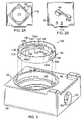
- a chamber liner 120 suitable for the chamber 22comprises first annular band 126 having a first diameter and a second annular band 128 having a second diameter, as shown in FIG. 2A .
- the second annular band 128is sized larger than diameter of the first annular band 126 .
- the second diameter of the second annular band 128can be at least about 2 cm larger than the first diameter of the first annular band 126 .
- the first annular band 126also comprises a first height and the second annular band 128 comprises a second height that is larger than the first height, for example, the second annular band 128 can have a second height that is at least 2 cm larger than the first height of the first annular band 126 .
- the first annular band 126has a first diameter of from about 12 inches to about 15 inches and a first height of from about 1.5 inches to about 2.5 inches; and the second annular band 128 has a second diameter of from about 15 inches to about 18 inches and a first height of from about 2.5 inches to about 4 inches.
- the chamber liner 120also has a first encased opening 139 which allows process gas to flow through the first and second annular bands 126 , 128 from the process zone 34 to the exhaust port 52 .
- the first opening 139is formed by the alignment of a first slot 140 a extending therethrough the first annular band 126 and a second slot 140 b passing through the second annular band 128 which is aligned to the first slot 140 a of the first annular band 126 .
- the aligned slots 140 a,bare surrounded by a flat top wall 142 and bottom wall 144 to form an encased first opening 139 .
- the first and second slots 140 a,bcomprise rectangles with rounded corners.
- the rectanglescan each have a length of from about 12 to 18 inches and a height of from about 0.75 to 3 inches.
- the aligned slots 140 a,ballow the passage of process gas species through the chamber liner 120 with reduced erosion of the corners and edges of the slots 140 a,b.
- the chamber liner 120can also have an additional second opening 149 in the first annular band 126 which opens to the exhaust port 52 .
- the first and second openings 139 , 149facilitate the passage of gas through the chamber liner 120 .
- the first opening 139allows passage of substrate 24 through the chamber liner 120 , for example by robot transport of the substrate 24 to and from the chamber 22 .
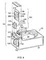
- the chamber 22also has an exhaust port 52 that receives spent process gas from the process zone 34 after the process gas passes over the substrate surface to exhaust the process gas from the chamber 22 and delivers the gas to an exhaust conduit 54 .
- the exhaust port 52is provided in a hollow exhaust block 152 which forms part of the sidewall 30 of the chamber.
- the hollow exhaust block 152comprises a rectangular inlet port 154 on an inner wall 155 , a circular outlet port 156 on an outer wall 157 , and a rectangular channel 158 therebetween, as shown in FIG. 4 .
- the hollow exhaust block 152is exposed to hot reactive process gas species gas that results in the deposition of process residue material on it interior surfaces. The accumulation of such process residue deposits is undesirable as these deposits flake off from the interior surfaces over time cause substrate contamination.
- an exhaust shield assembly 160is provided to protect, and provide easily replaceable and removable surfaces, around the exhaust port 52 and in the exhaust block 152 of the chamber 22 .
- An exemplary embodiment of an exhaust shield assembly 160comprises an assembly of component structures that cooperate together to provide good flow of process gas through this region while still allowing rapid removal and disassembly of the exhaust shield assembly 160 for cleaning or replacement of the component structures.
- the exhaust shield assembly 160can be easily removed and cleaned or replaced when excessive deposits form on their surfaces. Further, after use in a set number of process cycles, or a change in process gas composition, the removable exhaust shield assembly 160 can be discarded and replaced with a fresh exhaust shield assembly, to provide a consumable exhaust lining system. After removable from the chamber 22 , the exhaust shield assembly 160 can also be cleaned by rinsing with solvents and reused.
- the exhaust shield assembly 160comprises an inner shield 162 , pocket shield 164 , and outer shield 166 and cover shield 210 .
- the inner shield 162comprises an enclosed rectangular band 168 having a perimeter 170 defined by upper and lower planar walls 174 , 176 that are substantially parallel to one another and which are connected by arcuate end portions 178 a,b.
- the planar walls 174 , 176are separated by at least about 4 cm.
- a cross-sectional profile of the rectangular band 168is shaped like a rectangle with rounded corners.
- the arcuate end portions 178 a,b of the band 168can also be cylindrical, multi-radius curved, or even substantially flat.
- the inner shield 162is positioned on an inner wall 180 of a hollow exhaust block 152 in the chamber 22 and the enclosed rectangular band 168 is sized to fit over the rectangular inlet port 154 in the hollow exhaust block 152 .
- the inner shield 162also comprises a planar frame 172 extends perpendicularly beyond the perimeter of the rectangular band 168 .
- the planar frame 172is positioned at an outer end 190 of the inner shield 162 .
- the planar frame 172is placed flush against a matching rounded rectangular hole in the pocket shield 164 .
- the planar frame 172extends outward beyond the perimeter of the band by from about 3 to about 14 cm.
- the planar frame 172can be welded or brazed to the perimeter 170 of the rectangular band 168 and is usually made from the same material, that is, a sheet of aluminum.
- the pocket shield 164comprises a tubular encasing 194 having a top end 196 and a bottom end 198 .
- the tubular encasing 194has opposing first and second surfaces 200 , 202 which enclose a rectangular hollow sleeve.
- the first planar surface 200has an inner rectangular cutout 206 that fits the rectangular band 168 of the inner shield 162 so that process gas can flow thorough this passageway.
- the second planar surface 202has an outer circular cutout 208 which fits onto the outer shield 166 .
- a cover plate 210covers and closes off the top end 196 of the tubular encasing 194 .
- the bottom end 198 of the pocket shield 164has a well 212 which is adapted for fitting within the exhaust block 152 . In one version the well 212 is oval-shaped.
- the pocket shield 164is sized to fit inside the rectangular channel 158 of the hollow exhaust block 152 .
- the outer shield 166comprises first and second cylinders 212 , 214 that are joined to one another.
- the first cylinder 212is sized larger than the second cylinder 214 .
- the dimensions of the first and second cylinders 212 , 214are determined by the chamber geometry because the outer shield 166 is adapted to be positioned to be flush against the outer wall 157 of the hollow exhaust block 152 .
- the second cylinder 214 of the outer shield 166is sized to fit the circular outlet port 158 of the hollow exhaust block 152 .
- the outer shield 166has a height of from about 5.5 inches to about 7 inches, and a width of from about 5.5 inches to about 8 inches, and a depth of from about 1.4 to about 4 inches.
- a planar member 216is attached to the second cylinder 214 and extends perpendicularly beyond the second cylinder. In one version, the planar member 216 extends beyond the edge of the second cylinder 214 by from about 0.5 to about 1.5 inches.
- the inner shield 162 , pocket shield 164 , outer shield 166 and cover plate 210are all made from a metal, such as for example, aluminum, stainless steel, or titanium.
- the exhaust shield assembly 160is stamped and pressed out of aluminum sheets having a thickness of about 0.06 inches.
- the surfaces of the shield componentscan comprise bead-blasted surfaces for better adherence of process residues.
- the surfaceshave a surface roughness of about 40 to about 150 microinches, or even about 54 microinches. The surface roughness can also be obtained by wet sanding with a slurry comprising particles of from about 40 to about 125 microns in diameter or by dry sanding with a sandpaper comprising 120 to 400 grit.
- the components of the shield assembly 160tightly fit against and contact each other.
- the inner shield 162is in contact with the pocket shield 164 , and the planar frame 172 of the inner shield 162 is aligned with the slot of the pocket shield 164 .
- the surface of the outer shield 166is in contact with the first planar surface of the pocket shield 164 and the cover plate 210 covers the pocket shield 164 . It is not necessary for the shield components of the exhaust shield to form a gas tight seal with each other, but the components should have good contact with each other to reduce leakage of process gas from the exhaust block 152 .
- the substrate processing apparatus 20comprises an ALD chamber 22 a suitable for plasma ALD processes, as shown in FIG. 5 .
- the chamber 22 ahas a lid 29 that is adapted to provide good temperature characteristics for plasma ALD and can have heat exchange elements for cooling or heating of the chamber lid 29 a such as, for example, a water-cooled ceiling plate 31 as shown in FIG. 5 .
- the apparatus 20can also comprise remote or in-situ gas energizer elements, such as for example a remote gas energizer (model # ASTRO, available from MKS Instruments, Inc., Wilmington, Mass.), or electrical connectors, power supply and electrodes mounted in or about the chamber for in-situ plasma generation.
- a metal element of the chamber lid 29is used as a process electrode.
- one or more insulation rings 35can be provided between the chamber wall and ceiling to provide thermal or electrical insulation between the chamber components.
- a process gas supply 38 a or components of a process gas supply 38 acan be mounted on the chamber lid 29 and can include pneumatic valves, a process gas source 36 a or various tubes and channels for delivery of controlled levels of process and purge gasses to the process chamber 22 a during processing.
- the gas distributor 40 acomprises a central cap 60 a, a ceiling insert 37 and a showerhead 220 that fits into a bottom surface of the chamber lid 29 .
- the central cap 60 ahas one or more gas inlets 65 a,b, a gas outlet 66 a, and a gas passageway 70 a between the gas inlet 65 and gas outlet 66 a.
- the gas inlets 65 a,bare offset from one another in the horizontal plane and positioned around a circumference of the gas passageway 70 a.
- the offset gas inlets 65 a,bprovide individual gas streams that cooperate in the gas passageway 70 a to achieve a spiraling gas flow from the inlets 65 a,b to the outlet 66 a.
- the gas inlets 65 a,bcan be offset by being positioned at a separation angle of at least about 60 degrees, for example, about 180 degrees.
- the gas passageway 70 a in the cap 60 ais cylindrical and has a substantially uniform diameter through its length.
- the cap 60 arests on a ceiling insert 37 having and a conical passageway 43 therethrough for passage of process gas.
- the ceiling insert 37comprises ceramic or quartz and serves to electrically and thermally insulate the process gasses from the other components of the chamber lid 29 .
- the inlet 39 of the ceiling insert 37receives process gas from the outlet 66 a of the central cap 60 a.
- the conical passageway 43has a lower portion 45 that opens outward in the downward flow direction such that the diameter of the passageway 43 increases across the lower quarter of the ceiling insert 37 .
- the passageway 43terminates in an outlet 41 having a diameter that is about twice the diameter of the inlet 39 . This sudden opening of the passageway 43 allows adaptation to the larger receiving surface of the plasma screen 192 .
- the simultaneously injected gas streamsspin about a vertical axis 86 a through the passageway 70 a in a vortex motion to produce a spiral flow of gas heading downwards from the inlets 65 a,b to the outlet 41 of the ceiling insert 37 .
- the spiral flowmixes the gas and results in a more homogeneous mixture of gas at the outlet 41 .
- the vortex of process gasspirals from the outlet 41 of the ceiling insert 37 to a plasma screen 192 .
- the plasma screen 192comprises an annular plate 222 having a plurality of holes 224 which are spaced apart and distributed across the plasma screen 192 to screen the center of the channel from direct plasma passage.
- a central region 232 of the plasma screen 192has no holes therethrough, which prevents direct view of the RF electrodes.
- the number of holes 224 in the plasma screen 192can be from about 50 to about 400, and in one version, from about 150 to about 170.
- the holes 224have a diameter of from about 0.1 cm and about 0.3 cm.
- the plasma screen 192can also comprise a shaped peripheral lip 238 and raised circular band 242 about the holed region of the screen 220 , as shown in FIG. 8 .
- the peripheral lip 238 and circular band 242are shaped to form a seal with the ceiling insert 37 .
- the plasma screen 192comprises a ceramic.
- the plasma screen 192is annular in shape and has a thickness of from about 0.15 inches to about 1 inch.
- the plasma screen 192delivers process gas to a showerhead 220 gas distributor.
- the showerhead 220comprises a plate 226 having a plurality of holes 228 which are spaced apart and distributed across the showerhead 220 to evenly distribute the process gas across the substrate surface.
- the number of holes 228 in the showerhead 220can be from about 100 to about 10,000, and in one version, from about 500 to about 2500.
- the holes 228have a diameter of from about 0.01 and about 0.1 inches.
- the holes 228are shaped and sized to decrease in diameter between the upper surface and the lower surface of the plate 226 . This provides a reduction in back flow within the plate 226 .
- the showerhead 220comprises a metal such as aluminum, steel, or stainless steel.
- the showerhead 220is annular in shape and a thickness of from about 0.3 to about 2.5 inches.
- the showerhead 220comprises a peripheral region 230 that rests on an isolator 113 above the chamber sidewall 30 a and a central region 234 with a hole 236 bored through the center of the showerhead 220 to receive a gas distributor insert 240 .
- the gas distributor insert 240comprises an annular plate that is sized with a diameter sufficiently large to fit into the showerhead 220 .
- the annular platehas a central region and a peripheral region.
- the central region of the insert 240comprises a protrusion 244 having a flat annular top surface 248 and a side wall 250 that extends outward and downward from the flat annular surface 248 to the surface of the body region.
- the flat annular surface 248 of the insert 240contacts the central region of the plasma screen 192 .
- the annular plate of the gas distributor insert 240is composed of a metal, such as for example, aluminum.
- the gas distributor insert 240can be made by machining from a monolithic block.
- the gas distributor insert 240has a plurality of radial slots 252 that extend through the insert 240 to allow passage of process gas therethrough.
- the slots 252are spaced apart from one another and arranged in a radial configuration.
- the gas distributor insert 240has from about 5 about 50 slots 252 , for example about 20 slots 252 .
- each slot 252has a length of from about 0.4 to about 1.2 inches, and a width of from about 0.01 to about 0.05 inches.
- Each slot 252is oriented in the annular plate of the insert 240 to have a predefined radially or circumferential angle.
- the slots 252are angled through the plate and have a uniform pitch.
- the slots 252are arranged in this manner to maintain a vortex flow of the process gas through the gas distributor insert 240 .
- the pitch of the slots 252is chosen to optimize the vortex flow through the slots 252 and is between about 20 and about 70 degrees, or more typically about 45 degrees.
- the radially angled slots 252distribute the process gas above the substrate 24 to provide a uniform thickness of gas molecules adsorbed to the processing surface of the substrate 24 .
- the gas distributor insert 240has a plurality of cylindrical channels 246 that extend through the insert 240 about the center of the insert 240 to allow passage of process gas therethrough.
- the channels 246can comprise between 5 and 20 channels and in one version comprise 12 channels.
- the channels 246begin about the base of the protrusion 244 and terminate at the underside of the insert 240 .
- the cylindrical channels 246are arranged in a circular symmetric configuration about the base of the protrusion 244 and are tilted inwards such that the channels terminate at a position that is located below the protrusion 244 .
- the channels 246are angled at between 30 and 60 degrees to the vertical axis.
- the angled channels 246deliver process gas to the central region of the substrate surface and provide uniform deposition on the substrate.
- the diameter of the cylindrical channels 246is from about 0.01 to about 0.1 inches and in one version the diameter of the upper end of the channels 246 is greater than the diameter of the lower terminus of the channels 246 . This provides a reduction in back flow within the channels 246 .
- the process gas introduced into the chamber 22is energized by a gas energizer that couples energy to the process gas in the process zone 34 a of the chamber 22 a.
- the gas energizermay comprise process electrodes that may be electrically biased to energize the process gas; an antenna comprising an inductor coil which has a circular symmetry about the center of the chamber 22 a; or a microwave source and waveguide to activate the process gas by microwave energy in a remote zone upstream from the chamber 22 a.
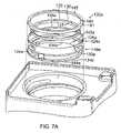
- a chamber liner 120 a suitable for use in plasma ALD chamber 22 ais shown in FIG. 7A .
- This version of the chamber liner 120 aalso covers a sidewall 30 a of the chamber 22 a to encircle the process zone 34 a and shield the walls of the chamber 22 a from the process gas.
- the chamber liner 120 ais made partially of a ceramic material, such as aluminum oxide (Al 2 O 3 )or aluminum nitride (AlN), and partially of a metal, such as aluminum or stainless steel.
- the chamber liner 120 acomprises first annular band 126 a having a first diameter and a second annular band 128 a having a second diameter that is larger than diameter of the first annular band 126 a, as shown in FIG.
- the second diameter of the second annular band 128 acan be at least about 1 cm larger than the first diameter of the first annular band 126 a.
- the first annular band 126 aalso comprises a first height and the second annular band 128 a comprises a second height that is at least 0.5 cm larger than the first height of the first annular band 126 a.
- the first and second annular bands 126 a, 128 a of the chamber liner 120 aare joined at their bottom edges 134 a,b by a radial flange 130 a which is circular in shape and a radial ledge 136 a further joins the midsection 138 a of the second annular band 128 a to the top edge 140 a of the first annular band 126 a of the chamber liner 120 a.
- the chamber liner 120 aalso has a first encased opening 139 a which allows process gas to flow through the first and second annular bands 126 a, 128 a from the process zone 34 a to the exhaust port 52 a.
- the first opening 139 ais formed by the alignment of a first slot 146 a extending therethrough the first annular band 126 a and a second slot 146 b passing through the second annular band 128 a which is aligned to the first slot 146 a of the first annular band 126 a.
- the aligned slots 146 a,bare surrounded by a flat top wall 142 a and bottom wall 144 a to form an encased first opening 139 a.
- the first and second slots 146 a,bcomprise rectangles with rounded corners.
- the rectanglescan each have a length of from about 12 to 18 inches and a height of from about 0.75 to 3 inches.
- the chamber liner 120 aalso has a second opening 149 a in the first annular band 126 a which opens to the exhaust port 52 a.
- the second opening 149 acomprises a rectangle having rounded corners, and which has a length of from about 5 to 9 inches and a height of from about 0.75 to 3 inches.
- the first and second openings 139 a, 149 afacilitate the passage of gas through the chamber liner 120 a.
- the chamber liner 120 aadditionally comprises a profiled inner shield ring 125 and an upper shield ring 145 .
- the inner shield ring 125has a diameter sized to encircle the substrate support 26 that faces the gas distributor 40 a in the ALD chamber 22 a.
- the inner shield ring 125serves as a partial physical barrier for the gasses in the process zone 34 a.
- the inner shield ring 125comprises a band having an upper, outwardly extending support lip 127 .
- the support lip 127 of the inner shield ring 125rests on the top edge 146 a of the first annular band 126 a of the chamber liner 120 a.
- the upper surface 129 of the bandis contoured such that a peripheral region is higher than a radially inner region.
- the upper surface 129comprises an inward angled portion 131 , a middle horizontal portion 133 , and an outer hump portion 135 . To minimize turbulence, these regions of the upper surface 129 are connected by smooth corners.
- the hump portion 133is situated above the outwardly extending lip 127 and has a height that is higher than the height of the periphery of the substrate support assembly by from about 0.01 to about 0.5 inches.
- the hump portion 133serves as a barrier to deter outward radial flow of the activated process gasses from the process region 38 a.
- the radially inner region of the inner shield ring 125extends inward from the first annular band 126 a by from about 0.2 to about 0.7 inches and defines one side of a gap 137 between the substrate support 26 and the chamber liner 120 a.
- the edges of the inner shield ring and of the substrate support assemblyare rounded about the gap 137 to decrease turbulence of the process gas during chamber purge steps. The decrease in turbulence provides a decrease in flow resistance, and allows for a more effective purge step.
- An upper shield ring 145rests on the upper surface of the second band 128 a.
- the upper shield ring 145shields an upper portion of the chamber sidewall 30 a and a peripheral portion of the ceiling assembly from the active gasses of the process zone 34 a, to reduce deposition of process gasses on and etching of the chamber body.
- the upper shield ring 145comprises an outer cylindrical band 141 capped by an inwardly extending ledge 143 .
- the ledge 143extends radially inward from the band 141 by from about 0.25 to about 1 inch.
- the upper shield ring 145comprises a ceramic and has a thickness of from about 0.25 to about 1 inch.
- the ALD chambers 22 , 22 a and their components described hereinsignificantly improve the thickness and compositional conformity of the atomic layer deposited onto a substrate 24 .
- the gas distributor 40 structureprovides a rapidly flowing vortex of gas molecules that more rapidly passes over the substrate 24 surface to provide better and more uniform gas adsorption on the substrate 24 surface.
- the gas vortexprevents the formation of gas molecule stagnation regions in the chamber 22 .
- atomic layer depositionis more uniform when the pressure of the reactant gas at the surface of the substrate 24 is uniform.
- the present gas distributor 40provides much better gas pressures across the substrate 24 surface to provide a more uniform thickness of the deposited ALD layer across the substrate 24 .
- the chamber liner 120 and exhaust shield assembly 160 componentsalso assist in the ALD process by allowing rapid withdrawal of gas species from the chamber 22 . This allows fresh gas molecules to adhere to the substrate 24 surface. Rapid withdrawal of the gas species enables the ALD chamber 22 to be effectively and efficiently purged between process gas steps. Further, when the process gas includes organic molecules or reactant gasses which have higher decay rates, the time between introduction of process gas, and hence the time required for an effective purge of the chamber 22 , is an important process parameter. Moreover, because the chamber liner 120 and exhaust shield components can be readily disassembled and removed from the chamber 22 , it reduces the chamber 22 downtime that would otherwise be required for cleaning or replacing these components.
- the present inventionhas been described with reference to certain preferred versions thereof; however, other versions are possible.
- the exhaust liner or components thereof and the chamber liners 120 , 120 acan be used in other types of applications, as would be apparent to one of ordinary skill, for example, etching, CVD and PVD chambers.
- the shapes of the flanges of the various componentscan be different, to interface with different chamber flanges and support walls.
- the materials of composition of the various componentscan be different for different applications such as composite ceramic or even fully ceramic materials for application in plasma excitation or hybrid etch processes. Therefore, the spirit and scope of the appended claims should not be limited to the description of the preferred versions contained herein.
Landscapes
- Chemical & Material Sciences (AREA)
- General Chemical & Material Sciences (AREA)
- Chemical Kinetics & Catalysis (AREA)
- Engineering & Computer Science (AREA)
- Materials Engineering (AREA)
- Mechanical Engineering (AREA)
- Metallurgy (AREA)
- Organic Chemistry (AREA)
- Chemical Vapour Deposition (AREA)
- Drying Of Semiconductors (AREA)
Abstract
Description
- Embodiments of the present invention relate to an atomic layer deposition chamber and its components.
- In the fabrication of integrated circuits and displays, an atomic layer deposition (ALD) chamber is used to deposit an atomic layer having a thickness on the order of atoms onto a substrate. Typically, the ALD chamber comprises an enclosure into which a process gas is introduced and an exhaust to exhaust and control the pressure of the process gas in the chamber. In one type of atomic layer deposition process, a first process gas introduced into the chamber to form a thin layer of gas molecules adsorbed onto the substrate surface; and thereafter, a second process gas is introduced to react with the adsorbed layer of gas molecules to from an atomic layer on the substrate. The process gases can include conventional pressurized gases or carrier gases to transport organic or other molecules into the chamber. Typically, the chamber is purged between the delivery of each process gas. The purge can be continuous in which a continuous flow of carrier gas is provided to the chamber or pulsed in which a discontinuous or pulsed flow of carrier gas is provided.
- Conventional substrate processing chambers used for CVD or PVD processes are being converted to ALD chambers because ALD processes are being increasingly used to deposit atomic layers on the substrate. However, conventional chambers do not always provide the sufficiently high levels of gas distribution, plasma, or thermal uniformity, required for ALD processes. For example, ALD chambers use particular types of gas distributors, shields, and exhaust components, all of which cooperate to provide more uniform delivery to, and removal of, process gas species from across the substrate surface. ALD converted chambers can also require specific components for different types of ALD processes, for example, thermal or plasma enhanced ALD (PEALD) processes. In thermal ALD, heat is provided to cause a chemical reaction between two or more reactants adsorbed onto a substrate surface. In thermal ALD, additional chamber components may be required to heat or cool the substrate or other chamber surfaces. PEALD processes require gas energizers to energize the process gas, and its components are designed to withstand etching by the energized process gas. Thus it is further desirable to have chamber conversion kits that can easily alter conventional chambers to ALD chambers.
- The ALD chamber components also need to provide good gas distribution uniformity across the substrate without inducing other adverse effects. For example, in plasma assisted ALD, providing a process gas stream that flows directly onto the substrate surface increases the possibility of adversely etching the substrate surface. Thermal ALD processes provide reduced gas efficiency when process gas species react with internal chamber surfaces instead of the substrate. Further, conventional showerhead gas distributors often provide process gas on the central region of the substrate at higher concentrations that at peripheral region of the substrate. It is also difficult to obtain uniform pressures of process gas species across the substrate surface during deposition. It is also sometimes desirable for the ALD chamber to be effectively purged between sequential process gas steps.
- Thus there is a need for ALD process kit and chamber components that can be used to retrofit conventional chambers. There is also a need for ALD chamber components that provide better gas, temperature and pressure uniformity across the substrate, while also allowing rapid purging of process gas.
- The following description, claims, and accompanying drawings, illustrate exemplary embodiments of different features which can be used by themselves, or in combination with other features, and should not be limited to the exemplary versions shown in the drawings:
FIG. 1 is a schematic sectional side view of an embodiment of a thermal ALD chamber;FIGS. 2A and 2B are a cross-sectional top view and a top planar view of an ceiling plate of the chamber lid of the ALD chamber ofFIG. 1 , showing a heat transfer fluid conduit having a rectangular shape;FIG. 3 is a perspective view of a chamber liner that can be used in the ALD chamber ofFIG. 1 ;FIG. 4 is an exploded perspective view of an exhaust shield assembly of the ALD chamber ofFIG. 1 ;FIG. 5 is a schematic sectional side view of an embodiment of a PEALD chamber;FIG. 6A is a schematic bottom view of a chamber lid of the PEALD chamber ofFIG. 5 , the chamber lid having a gas distributor with a fan-type insert;FIG. 6B is a cross-sectional perspective view of the fan-type insert ofFIG. 6A ;FIG. 7A is a perspective view of a chamber liner of the PEALD chamber ofFIG. 5 ;FIG. 7B is a cross-sectional view of the chamber liner ofFIG.7A ; andFIG. 8 is a perspective view of a plasma screen of the PEALD chamber ofFIG. 5 .- An embodiment of a
substrate processing apparatus 20 comprising an atomic layer deposition (ALD)chamber 22 is shown inFIG. 1 . Thechamber 22 is suitable for thermal ALD processes for deposition of an atomic layer on asubstrate 24 resting on asubstrate support 26. In thermal ALD processes, process gas molecules adsorbed onto asubstrate 24 are heated to temperatures sufficiently high to form an atomic layer on thesubstrate 24. Suitable thermal ALD temperatures can be, for example, from about 120° C. to about 450° C. Thechamber 22 is suitable forprocessing substrates 24 such as semiconductor wafers, however, thechamber 22 can be adapted to processother substrates 24, such as for example, flat panel displays, polymer panels, or other electrical circuit receiving structures, as would be apparent to those of ordinary skill in the art. Theapparatus 20 can also be attached to a platform (not shown) that provides electrical, plumbing, and other support functions for thechamber 22, and which can also be part of a multi-chamber platform system such as, for example, the DaVinci or Endura II platform, available from Applied Materials Inc., Santa Clara, Calif. - Generally, the
chamber 22 is enclosed by aceiling 28,sidewall 30, andbottom wall 32. Thesubstrate support 26 extends through thebottom wall 32 to support thesubstrate 24 on asubstrate receiving surface 33. The substrate support26 together with thesidewall 30 defines aprocess zone 34 in which process gas is provided to process thesubstrate 24. In operation, process gas is introduced into thechamber 22 through agas supply 36 that includes aprocess gas source 38 andgas distributor 40. Thegas distributor 40 may comprise one ormore conduits 42 to provide gas having agas supply valve 44 therein, and agas outlet 6646 to release the process gas into theprocess zone 34 of thechamber 22. For ALD processes, theprocess gas source 38 can be used to supply different process gases that can each contain a single gas or a mixture of gases, a carrier gas and transported molecule, or a purge gas which may also be the carrier gas. Spent process gas and process byproducts are exhausted from thechamber 22 through anexhaust system 50 which may include anexhaust port 52 that receives spent process gas from theprocess zone 34 and delivers the gas to anexhaust conduit 54, and a throttle valve and exhaust pumps (not shown) to control the pressure of process gas in thechamber 22. - The
gas distributor 40 comprises acentral cap 60 having one ormore gas inlets 64a,b,agas outlet 66, and agas passageway 70 between thegas inlet 64 andgas outlet 66. Thegas inlets 64a,b are offset from one another in the horizontal plane and positioned around a circumference of thegas passageway 70. Theoffset gas inlets 64a,bprovide individual gas streams that cooperate in thegas passageway 70 to achieve a spiraling gas flow from theinlets 64a,bto theoutlet 66. In one version, thegas inlets 64a,bcan be offset by being positioned at a separation angle of at least about 45 degrees, for example, about 180 degrees. Thetop portion 74 of thegas passageway 70 in thecap 60 is cylindrical. Thebottom portion 76 of thegas passageway 70 comprises aconical passageway 78 which gradually opens outward in the downward gas flow direction with the radius of the inner diameter of theconical passageway 78 increasing from a first diameter at anupper region 80 to a second larger diameter at alower region 82 about theoutlet 66 of thecap 60. In one version, the first diameter is less than about 2.6 cm and the second diameter is at least about 3 cm. For example, the first diameter can be from about 0.2 cm to about 2.6 cm and the second diameter can be from about 3 cm to about 7.5 cm. Theconical passageway 78 can also have a surface that is inclined relative to the vertical axis at an angle of from about 5° to about 30° or more typically about 11°. - When process gas is injected into the
cap 60 through theoffset gas inlets 64a,b,the simultaneously injected gas streams spin about avertical axis 86 through theconical passageway 78 in a vortex motion to produce a spiral flow of gas heading downwards from theinlets 64a,bto theoutlet 66. Advantageously, the angular momentum of the spiraling gas causes the gas to sweep the surface of theconical passageway 78. Also, the gradual increase in diameter of theconical passageway 78 from the first diameter to the second diameter, produces an increasing volume of the gas, which results in a corresponding increase in the width of the gas vortex and a gradual reduction in gas pressure and temperature, both of which are desirable because they inhibit condensation of the precursor gas and reduce the vertical speed of the gas onto thesubstrate 24. Further, the rotational energy and angular momentum of the process gas about thevertical axis 86 of theconical passageway 78 decreases as the process gas descends along the passageway. Theconical passageway 78 is bell shaped to allow the process gas vortex to fan out as it enters thechamber 22 and thereby providing a better distribution of the process gas directly above thesubstrate 24. - The
central cap 60 rests on a shapedceiling plate 90 which in one version is funnel-shaped. The shapedceiling plate 90 serves as a chamber lid, and has interconnected first and secondconical apertures conical aperture 92 receives a process gas from thegas outlet 66 and has a first diameter, and the secondconical aperture 94 releases the process gas and has a second diameter that is larger than the first diameter. Each of theconical apertures ceiling plate cap 90 is composed of aluminum such as for example aluminum alloy. - The first conical aperture in92 the shaped
ceiling plate 90 connects to theoutlet 66 of thecentral cap 60 and has a narrower first diameter at aninterface surface 98 between theceiling plate 90 and thecentral cap 60, which gradually increases to a larger diameter at the segment joint96 that joins to the secondconical aperture 94. In one version, the gradually tapered surface of the firstconical aperture 92 comprises a conical surface with an inclination angle of from about 50° to about 30° relative to the vertical axis. The segment joint96 comprises a rounded edge and provides a gradual transition between the slopes of the first and secondconical apertures conical aperture 94 extends radially outward with an increasing diameter from a first diameter at the segment joint96 to a second larger diameter above anouter perimeter 100 of thesubstrate support 26. The surface of the secondconical aperture 94 has a conical surface with an inclination angle of from about 1° to about 15° relative to the vertical axis. - The shaped
ceiling plate 90 also has aperipheral ledge 104 that extends radially outwardly out from thegas distributor 40 and above theouter perimeter 100 of thesubstrate support 26. Thelower surface 106 of theperipheral ledge 104 is substantially horizontal to allow theperipheral ledge 104 to rest about thesidewall 30 of thechamber 22 to support theceiling plate 90 above theprocess zone 34. Theperipheral ledge 104 has a stepped down height with an intermediate step108 that smoothly curves upwards from the secondconical aperture 94 to theperipheral ledge 104. - The shaped
conical passageway 78 through thecentral cap 60, and the first and secondconical apertures ceiling plate 90, also allow process gas or purge gas to pass through with minimum flow resistance and provide good distribution across a surface of thesubstrate 24. Theconical passageway 78 increases in diameter as the gas descends into thechamber 22. The width of the spirally descending process gas vortex likewise increases to provide a high velocity gas flow. The rotational energy and angular momentum of the process gas about thevertical axis 86 of theconical passageway 78 decreases as the process gas descends along the passageway. The portion of the gas passageway within theceiling plate 90 has a diameter that increases between the top and bottom of theceiling plate 90. Thus, the entire gas passageway through thecap 60 andceiling plate 90 is bell shaped to allow the process gas vortex to fan out as it enters thechamber 22, thereby uniformly distributing the process gas into theprocess zone 34 of thechamber 22 directly above thesubstrate 24. - The
gas distributor 40 can also comprise atemperature regulating system 110 which includes heating or cooling elements and temperature sensors. The ceiling mountedgas distributor 40 takes up much of the surface area in the region of the process zone. Thus it is desirable to control the temperature of thegas distributor 40 to control its effect on the process gas about thesubstrate 24. If thegas distributor 40 is too hot, for example, the process gas can react at its surfaces to deposit material at these surfaces instead of on thesubstrate 24. Alternatively excessive cooling of thegas distributor 40 can cause the process gas to be excessively cool in temperature when it reaches thesubstrate 24. Thus, it is desirable to control the temperatures of thegas distributor 40 to maintain temperatures that provide optimum delivery of the process gas to thesubstrate 24. - In one version, the
temperature regulating system 110 comprises heat transfer fluid conduits112 that contact thegas distributor 40, for example, contacting thecap 60, theceiling plate 90, or both. Thetemperature regulating system 110 can include afluid conduit 116 for passing heat transfer fluid therethrough to remove or add heat to the process gas. In one version, thefluid conduit 116 comprises a channel that is machined through theceiling plate 90, as shown inFIG. 2A . This allows thefluid conduit 116 to also control the temperature of the process gas as it passes through thegas passageway 70 which extends through thecentral cap 60 and theceiling plate 90. For example, when the process gas passing through this region rapidly changes in temperature because of expansion of the gas arising from the different volumes of theconical passageway 78 and firstconical aperture 92, the change in gas temperature can be regulated by passing a heat transfer fluid maintained at a desired temperature differential through thefluid conduit 116. The heat transfer fluid exchanges heat with the process gas passing through thegas distributor 40 to regulate its temperature. The temperature of the heat transfer fluid is regulated using a conventional heat exchange system (not shown) external to thechamber 22, comprising for example, a pump connecting a fluid reservoir comprising a heat transfer fluid such as deionized water, to thefluid conduits 116 and including a heating or refrigeration system to heat or cool the fluid in thefluid conduit 116. - The process gas passed into the
chamber 22 is contained about the processing region of asubstrate 24 by achamber liner 120 which at least partially covers asidewall 30 of thechamber 22 to encircle theprocess zone 34. Thechamber liner 120 serves to shield the walls of thechamber 22 from the process gas and also to confine the process gas to the region above thesubstrate 24. Thechamber liner 120 is typically shaped to at least partially conform to thechamber sidewall 30. Thechamber liner 120 also hasgas openings 124 to allow process gas to flow therethrough from theprocess zone 34 to theexhaust port 52. Thechamber liner 120 can be made from a metal, such as aluminum or a ceramic. - A
chamber liner 120 suitable for thechamber 22 comprises first annular band126 having a first diameter and a secondannular band 128 having a second diameter, as shown inFIG. 2A . The secondannular band 128 is sized larger than diameter of the first annular band126. For example, the second diameter of the secondannular band 128 can be at least about2 cm larger than the first diameter of the first annular band126. The first annular band126 also comprises a first height and the secondannular band 128 comprises a second height that is larger than the first height, for example, the secondannular band 128 can have a second height that is at least 2 cm larger than the first height of the first annular band126. In one version, the first annular band126 has a first diameter of from about 12 inches to about 15 inches and a first height of from about 1.5 inches to about 2.5 inches; and the secondannular band 128 has a second diameter of from about 15 inches to about 18 inches and a first height of from about 2.5 inches to about 4 inches. - The first and second
annular bands 126,128 of thechamber liner 120 are structurally joined together at their bottom edges132a,bby aradial flange 130 which is circular in shape. Theradial flange 130 serves to hold the first and secondannular bands 126,128 in a spaced apart gap in the radial direction. Theradial flange 130 can be sized to provide a radial gap of at least about 38 mm, for example, from about 25 to about 50 mm. Aradial ledge 136 further joins themidsection 138 of the secondannular band 128 to thetop edge 140 of the first annular band126 of thechamber liner 120. Theradial ledge 136 provides additional structural integrity to thechamber liner 120. Theradial ledge 136 extends across a portion of the inner circumference of thechamber liner 120, for example, to cover from about 0 to about 1800 of the inner circumference. As a result, an open gap region is provided across the remaining portion of the inner circumference to provide easier flow and passage of process gas through thechamber liner 120. - The
chamber liner 120 also has a first encasedopening 139 which allows process gas to flow through the first and secondannular bands 126,128 from theprocess zone 34 to theexhaust port 52. Thefirst opening 139 is formed by the alignment of afirst slot 140aextending therethrough the first annular band126 and asecond slot 140bpassing through the secondannular band 128 which is aligned to thefirst slot 140aof the first annular band126. The alignedslots 140a,bare surrounded by a flattop wall 142 andbottom wall 144 to form an encasedfirst opening 139. In one version, the first andsecond slots 140a,bcomprise rectangles with rounded corners. For example, the rectangles can each have a length of from about 12 to 18 inches and a height of from about 0.75 to 3 inches. The alignedslots 140a,ballow the passage of process gas species through thechamber liner 120 with reduced erosion of the corners and edges of theslots 140a,b.Thechamber liner 120 can also have an additionalsecond opening 149 in the first annular band126 which opens to theexhaust port 52. The first andsecond openings chamber liner 120. In one version, thefirst opening 139 allows passage ofsubstrate 24 through thechamber liner 120, for example by robot transport of thesubstrate 24 to and from thechamber 22. - The
chamber 22 also has anexhaust port 52 that receives spent process gas from theprocess zone 34 after the process gas passes over the substrate surface to exhaust the process gas from thechamber 22 and delivers the gas to anexhaust conduit 54. Theexhaust port 52 is provided in ahollow exhaust block 152 which forms part of thesidewall 30 of the chamber. Thehollow exhaust block 152 comprises arectangular inlet port 154 on an inner wall155, acircular outlet port 156 on anouter wall 157, and arectangular channel 158 therebetween, as shown inFIG. 4 . Thehollow exhaust block 152 is exposed to hot reactive process gas species gas that results in the deposition of process residue material on it interior surfaces. The accumulation of such process residue deposits is undesirable as these deposits flake off from the interior surfaces over time cause substrate contamination. The accumulation of such process gas deposits onto the exhaust surfaces can be fixed by cleaning out the interior surfaces of theexhaust block 152 but this requires dismantling of thechamber 22 as the exhaust block is often an integral part of thechamber 22, which is time consuming and results in excessive chamber downtime. Problems also arise when the composition of the process gas used in thechamber 22 is changed or other because the deposits already accumulated onto the interior surfaces of theexhaust block 152 can react with the new gas species in an undesirable manner. - Thus, an
exhaust shield assembly 160 is provided to protect, and provide easily replaceable and removable surfaces, around theexhaust port 52 and in theexhaust block 152 of thechamber 22. An exemplary embodiment of anexhaust shield assembly 160, as shown for example inFIG. 4 , comprises an assembly of component structures that cooperate together to provide good flow of process gas through this region while still allowing rapid removal and disassembly of theexhaust shield assembly 160 for cleaning or replacement of the component structures. Theexhaust shield assembly 160 can be easily removed and cleaned or replaced when excessive deposits form on their surfaces. Further, after use in a set number of process cycles, or a change in process gas composition, the removableexhaust shield assembly 160 can be discarded and replaced with a fresh exhaust shield assembly, to provide a consumable exhaust lining system. After removable from thechamber 22, theexhaust shield assembly 160 can also be cleaned by rinsing with solvents and reused. - In one version, the
exhaust shield assembly 160 comprises aninner shield 162,pocket shield 164, andouter shield 166 andcover shield 210. Theinner shield 162 comprises an enclosedrectangular band 168 having aperimeter 170 defined by upper and lowerplanar walls 174,176 that are substantially parallel to one another and which are connected byarcuate end portions 178a,b.In one version, theplanar walls 174,176 are separated by at least about 4 cm. A cross-sectional profile of therectangular band 168 is shaped like a rectangle with rounded corners. However, thearcuate end portions 178a,bof theband 168 can also be cylindrical, multi-radius curved, or even substantially flat. Theinner shield 162 is positioned on an inner wall180 of ahollow exhaust block 152 in thechamber 22 and the enclosedrectangular band 168 is sized to fit over therectangular inlet port 154 in thehollow exhaust block 152. - The
inner shield 162 also comprises aplanar frame 172 extends perpendicularly beyond the perimeter of therectangular band 168. Theplanar frame 172 is positioned at an outer end190 of theinner shield 162. Theplanar frame 172 is placed flush against a matching rounded rectangular hole in thepocket shield 164. In one version, theplanar frame 172 extends outward beyond the perimeter of the band by from about 3 to about 14 cm. Theplanar frame 172 can be welded or brazed to theperimeter 170 of therectangular band 168 and is usually made from the same material, that is, a sheet of aluminum. - The
pocket shield 164 comprises atubular encasing 194 having atop end 196 and abottom end 198. Thetubular encasing 194 has opposing first andsecond surfaces 200,202 which enclose a rectangular hollow sleeve. The firstplanar surface 200 has an inner rectangular cutout206 that fits therectangular band 168 of theinner shield 162 so that process gas can flow thorough this passageway. The second planar surface202 has an outercircular cutout 208 which fits onto theouter shield 166. Acover plate 210 covers and closes off thetop end 196 of thetubular encasing 194. Thebottom end 198 of thepocket shield 164 has a well212 which is adapted for fitting within theexhaust block 152. In one version the well212 is oval-shaped. Thepocket shield 164 is sized to fit inside therectangular channel 158 of thehollow exhaust block 152. - The
outer shield 166 comprises first andsecond cylinders first cylinder 212 is sized larger than thesecond cylinder 214. The dimensions of the first andsecond cylinders outer shield 166 is adapted to be positioned to be flush against theouter wall 157 of thehollow exhaust block 152. Thesecond cylinder 214 of theouter shield 166 is sized to fit thecircular outlet port 158 of thehollow exhaust block 152. In one version, theouter shield 166 has a height of from about 5.5 inches to about 7 inches, and a width of from about 5.5 inches to about8 inches, and a depth of from about 1.4 to about 4 inches. Aplanar member 216 is attached to thesecond cylinder 214 and extends perpendicularly beyond the second cylinder. In one version, theplanar member 216 extends beyond the edge of thesecond cylinder 214 by from about 0.5 to about 1.5 inches. - In one version, the
inner shield 162,pocket shield 164,outer shield 166 andcover plate 210, are all made from a metal, such as for example, aluminum, stainless steel, or titanium. In one version, theexhaust shield assembly 160 is stamped and pressed out of aluminum sheets having a thickness of about 0.06 inches. In addition, the surfaces of the shield components can comprise bead-blasted surfaces for better adherence of process residues. In one version, the surfaces have a surface roughness of about 40 to about 150 microinches, or even about 54 microinches. The surface roughness can also be obtained by wet sanding with a slurry comprising particles of from about 40 to about 125 microns in diameter or by dry sanding with a sandpaper comprising 120 to 400 grit. - When the
exhaust shield assembly 160 is installed in thehollow exhaust block 152, the components of theshield assembly 160 tightly fit against and contact each other. Theinner shield 162 is in contact with thepocket shield 164, and theplanar frame 172 of theinner shield 162 is aligned with the slot of thepocket shield 164. The surface of theouter shield 166 is in contact with the first planar surface of thepocket shield 164 and thecover plate 210 covers thepocket shield 164. It is not necessary for the shield components of the exhaust shield to form a gas tight seal with each other, but the components should have good contact with each other to reduce leakage of process gas from theexhaust block 152. - Another embodiment of the
substrate processing apparatus 20 comprises anALD chamber 22asuitable for plasma ALD processes, as shown inFIG. 5 . Thechamber 22ahas alid 29 that is adapted to provide good temperature characteristics for plasma ALD and can have heat exchange elements for cooling or heating of the chamber lid29asuch as, for example, a water-cooledceiling plate 31 as shown inFIG. 5 . Theapparatus 20 can also comprise remote or in-situ gas energizer elements, such as for example a remote gas energizer (model # ASTRO, available from MKS Instruments, Inc., Wilmington, Mass.), or electrical connectors, power supply and electrodes mounted in or about the chamber for in-situ plasma generation. In some chambers, a metal element of thechamber lid 29 is used as a process electrode. Also, one or more insulation rings35 can be provided between the chamber wall and ceiling to provide thermal or electrical insulation between the chamber components. Aprocess gas supply 38aor components of aprocess gas supply 38acan be mounted on thechamber lid 29 and can include pneumatic valves, aprocess gas source 36aor various tubes and channels for delivery of controlled levels of process and purge gasses to theprocess chamber 22aduring processing. - In the chamber shown in
FIG. 5 , the gas distributor40acomprises acentral cap 60a,aceiling insert 37 and ashowerhead 220 that fits into a bottom surface of thechamber lid 29. Thecentral cap 60ahas one ormore gas inlets 65a,b,agas outlet 66a,and agas passageway 70abetween the gas inlet65 andgas outlet 66a.Thegas inlets 65a,bare offset from one another in the horizontal plane and positioned around a circumference of thegas passageway 70a.The offsetgas inlets 65a,bprovide individual gas streams that cooperate in thegas passageway 70ato achieve a spiraling gas flow from theinlets 65a,bto theoutlet 66a.In one version, thegas inlets 65a,bcan be offset by being positioned at a separation angle of at least about60 degrees, for example, about180 degrees. Thegas passageway 70ain thecap 60ais cylindrical and has a substantially uniform diameter through its length. - The
cap 60arests on aceiling insert 37 having and a conical passageway43 therethrough for passage of process gas. Theceiling insert 37 comprises ceramic or quartz and serves to electrically and thermally insulate the process gasses from the other components of thechamber lid 29. Theinlet 39 of theceiling insert 37 receives process gas from theoutlet 66aof thecentral cap 60a.The conical passageway43 has alower portion 45 that opens outward in the downward flow direction such that the diameter of the passageway43 increases across the lower quarter of theceiling insert 37. The passageway43 terminates in an outlet41 having a diameter that is about twice the diameter of theinlet 39. This sudden opening of the passageway43 allows adaptation to the larger receiving surface of theplasma screen 192. - When process gas is injected into the
cap 60athrough the offsetgas inlets 65a,b,the simultaneously injected gas streams spin about a vertical axis86athrough thepassageway 70ain a vortex motion to produce a spiral flow of gas heading downwards from theinlets 65a,bto the outlet41 of theceiling insert 37. Advantageously, the spiral flow mixes the gas and results in a more homogeneous mixture of gas at the outlet41. - The vortex of process gas spirals from the outlet41 of the
ceiling insert 37 to aplasma screen 192. Theplasma screen 192 comprises an annular plate222 having a plurality ofholes 224 which are spaced apart and distributed across theplasma screen 192 to screen the center of the channel from direct plasma passage. In one version acentral region 232 of theplasma screen 192 has no holes therethrough, which prevents direct view of the RF electrodes. The number ofholes 224 in theplasma screen 192 can be from about 50 to about 400, and in one version, from about 150 to about 170. In one version, theholes 224 have a diameter of from about 0.1 cm and about 0.3 cm. Theplasma screen 192 can also comprise a shapedperipheral lip 238 and raisedcircular band 242 about the holed region of thescreen 220, as shown inFIG. 8 . Theperipheral lip 238 andcircular band 242 are shaped to form a seal with theceiling insert 37. In one version, theplasma screen 192 comprises a ceramic. Theplasma screen 192 is annular in shape and has a thickness of from about 0.15 inches to about 1 inch. - The
plasma screen 192 delivers process gas to ashowerhead 220 gas distributor. Theshowerhead 220 comprises aplate 226 having a plurality of holes228 which are spaced apart and distributed across theshowerhead 220 to evenly distribute the process gas across the substrate surface. The number of holes228 in theshowerhead 220 can be from about 100 to about 10,000, and in one version, from about 500 to about 2500. In one version, the holes228 have a diameter of from about 0.01 and about 0.1 inches. In one embodiment, the holes228 are shaped and sized to decrease in diameter between the upper surface and the lower surface of theplate 226. This provides a reduction in back flow within theplate 226. In one version, theshowerhead 220 comprises a metal such as aluminum, steel, or stainless steel. Theshowerhead 220 is annular in shape and a thickness of from about 0.3 to about 2.5 inches. - The
showerhead 220 comprises aperipheral region 230 that rests on an isolator113 above thechamber sidewall 30aand acentral region 234 with ahole 236 bored through the center of theshowerhead 220 to receive agas distributor insert 240. Thegas distributor insert 240 comprises an annular plate that is sized with a diameter sufficiently large to fit into theshowerhead 220. The annular plate has a central region and a peripheral region. The central region of theinsert 240 comprises aprotrusion 244 having a flat annulartop surface 248 and aside wall 250 that extends outward and downward from the flatannular surface 248 to the surface of the body region. In one version the flatannular surface 248 of theinsert 240 contacts the central region of theplasma screen 192. In one version, the annular plate of thegas distributor insert 240 is composed of a metal, such as for example, aluminum. Thegas distributor insert 240 can be made by machining from a monolithic block. - The
gas distributor insert 240 has a plurality ofradial slots 252 that extend through theinsert 240 to allow passage of process gas therethrough. Theslots 252 are spaced apart from one another and arranged in a radial configuration. For example, in one version, thegas distributor insert 240 has from about5 about50slots 252, for example about20slots 252. In one version, eachslot 252 has a length of from about 0.4 to about 1.2 inches, and a width of from about 0.01 to about 0.05 inches. Eachslot 252 is oriented in the annular plate of theinsert 240 to have a predefined radially or circumferential angle. Theslots 252 are angled through the plate and have a uniform pitch. Theslots 252 are arranged in this manner to maintain a vortex flow of the process gas through thegas distributor insert 240. The pitch of theslots 252 is chosen to optimize the vortex flow through theslots 252 and is between about 20 and about 70 degrees, or more typically about45 degrees. The radially angledslots 252 distribute the process gas above thesubstrate 24 to provide a uniform thickness of gas molecules adsorbed to the processing surface of thesubstrate 24. - In one embodiment the
gas distributor insert 240 has a plurality ofcylindrical channels 246 that extend through theinsert 240 about the center of theinsert 240 to allow passage of process gas therethrough. Thechannels 246 can comprise between 5 and 20 channels and in one version comprise12 channels. Thechannels 246 begin about the base of theprotrusion 244 and terminate at the underside of theinsert 240. Thecylindrical channels 246 are arranged in a circular symmetric configuration about the base of theprotrusion 244 and are tilted inwards such that the channels terminate at a position that is located below theprotrusion 244. In one embodiment thechannels 246 are angled at between 30 and 60 degrees to the vertical axis. Theangled channels 246 deliver process gas to the central region of the substrate surface and provide uniform deposition on the substrate. The diameter of thecylindrical channels 246 is from about 0.01 to about 0.1 inches and in one version the diameter of the upper end of thechannels 246 is greater than the diameter of the lower terminus of thechannels 246. This provides a reduction in back flow within thechannels 246. - In this embodiment, the process gas introduced into the
chamber 22 is energized by a gas energizer that couples energy to the process gas in theprocess zone 34aof thechamber 22a.For example, the gas energizer may comprise process electrodes that may be electrically biased to energize the process gas; an antenna comprising an inductor coil which has a circular symmetry about the center of thechamber 22a;or a microwave source and waveguide to activate the process gas by microwave energy in a remote zone upstream from thechamber 22a. - A
chamber liner 120asuitable for use inplasma ALD chamber 22ais shown inFIG. 7A . This version of thechamber liner 120aalso covers asidewall 30aof thechamber 22ato encircle theprocess zone 34aand shield the walls of thechamber 22afrom the process gas. Thechamber liner 120ais made partially of a ceramic material, such as aluminum oxide (Al2O3)or aluminum nitride (AlN), and partially of a metal, such as aluminum or stainless steel. Thechamber liner 120acomprises firstannular band 126ahaving a first diameter and a secondannular band 128ahaving a second diameter that is larger than diameter of the firstannular band 126a,as shown inFIG. 7A . For example, the second diameter of the secondannular band 128acan be at least about 1 cm larger than the first diameter of the firstannular band 126a.The firstannular band 126aalso comprises a first height and the secondannular band 128acomprises a second height that is at least 0.5 cm larger than the first height of the firstannular band 126a.The first and secondannular bands chamber liner 120aare joined at theirbottom edges 134a,bby aradial flange 130awhich is circular in shape and a radial ledge136afurther joins the midsection138aof the secondannular band 128ato thetop edge 140aof the firstannular band 126aof thechamber liner 120a. - The
chamber liner 120aalso has a first encased opening139awhich allows process gas to flow through the first and secondannular bands process zone 34ato the exhaust port52a.The first opening139ais formed by the alignment of a first slot146aextending therethrough the firstannular band 126aand a second slot146bpassing through the secondannular band 128awhich is aligned to the first slot146aof the firstannular band 126a.The aligned slots146a,bare surrounded by a flattop wall 142aandbottom wall 144ato form an encased first opening139a.In one version, the first and second slots146a,bcomprise rectangles with rounded corners. For example, the rectangles can each have a length of from about 12 to 18 inches and a height of from about 0.75 to 3 inches. Thechamber liner 120aalso has asecond opening 149ain the firstannular band 126awhich opens to the exhaust port52a.Thesecond opening 149acomprises a rectangle having rounded corners, and which has a length of from about 5 to 9 inches and a height of from about 0.75 to 3 inches. The first andsecond openings 139a,149afacilitate the passage of gas through thechamber liner 120a. - The
chamber liner 120aadditionally comprises a profiledinner shield ring 125 and anupper shield ring 145. Referring toFIG. 7A andFIG. 7B theinner shield ring 125 has a diameter sized to encircle thesubstrate support 26 that faces the gas distributor40ain theALD chamber 22a.Theinner shield ring 125 serves as a partial physical barrier for the gasses in theprocess zone 34a.Theinner shield ring 125 comprises a band having an upper, outwardly extendingsupport lip 127. Thesupport lip 127 of theinner shield ring 125 rests on the top edge146aof the firstannular band 126aof thechamber liner 120a. - The
upper surface 129 of the band is contoured such that a peripheral region is higher than a radially inner region. Theupper surface 129 comprises an inwardangled portion 131, a middle horizontal portion133, and anouter hump portion 135. To minimize turbulence, these regions of theupper surface 129 are connected by smooth corners. The hump portion133 is situated above the outwardly extendinglip 127 and has a height that is higher than the height of the periphery of the substrate support assembly by from about 0.01 to about 0.5 inches. The hump portion133 serves as a barrier to deter outward radial flow of the activated process gasses from theprocess region 38a. - The radially inner region of the
inner shield ring 125 extends inward from the firstannular band 126aby from about 0.2 to about 0.7 inches and defines one side of agap 137 between thesubstrate support 26 and thechamber liner 120a.The edges of the inner shield ring and of the substrate support assembly are rounded about thegap 137 to decrease turbulence of the process gas during chamber purge steps. The decrease in turbulence provides a decrease in flow resistance, and allows for a more effective purge step. - An
upper shield ring 145 rests on the upper surface of thesecond band 128a.Theupper shield ring 145 shields an upper portion of thechamber sidewall 30aand a peripheral portion of the ceiling assembly from the active gasses of theprocess zone 34a,to reduce deposition of process gasses on and etching of the chamber body. Theupper shield ring 145 comprises an outercylindrical band 141 capped by an inwardly extendingledge 143. Theledge 143 extends radially inward from theband 141 by from about 0.25 to about 1 inch. Theupper shield ring 145 comprises a ceramic and has a thickness of from about 0.25 to about 1 inch. - The
ALD chambers substrate 24. For example, thegas distributor 40 structure provides a rapidly flowing vortex of gas molecules that more rapidly passes over thesubstrate 24 surface to provide better and more uniform gas adsorption on thesubstrate 24 surface. Also the gas vortex prevents the formation of gas molecule stagnation regions in thechamber 22. Further, atomic layer deposition is more uniform when the pressure of the reactant gas at the surface of thesubstrate 24 is uniform. Thepresent gas distributor 40 provides much better gas pressures across thesubstrate 24 surface to provide a more uniform thickness of the deposited ALD layer across thesubstrate 24. - The
chamber liner 120 andexhaust shield assembly 160 components also assist in the ALD process by allowing rapid withdrawal of gas species from thechamber 22. This allows fresh gas molecules to adhere to thesubstrate 24 surface. Rapid withdrawal of the gas species enables theALD chamber 22 to be effectively and efficiently purged between process gas steps. Further, when the process gas includes organic molecules or reactant gasses which have higher decay rates, the time between introduction of process gas, and hence the time required for an effective purge of thechamber 22, is an important process parameter. Moreover, because thechamber liner 120 and exhaust shield components can be readily disassembled and removed from thechamber 22, it reduces thechamber 22 downtime that would otherwise be required for cleaning or replacing these components. - The present invention has been described with reference to certain preferred versions thereof; however, other versions are possible. For example, the exhaust liner or components thereof and the
chamber liners
Claims (36)
1. An atomic layer deposition chamber comprising:
(a) a sidewall surrounding a bottom wall;
(b) a substrate support extending through the bottom wall;
(c) a gas distributor comprising:
(i) a central cap comprising at least one gas inlet, a gas outlet, and a conical passageway between the gas inlet and gas outlet; and
(ii) a ceiling plate comprising a first conical aperture that receives a process gas from the gas outlet of the central cap, a second conical aperture extending radially outwardly from the first conical aperture, and a peripheral ledge that rests on the sidewall of the chamber; and
(d) an exhaust port to exhaust the process gas from the process zone.
2. A chamber according toclaim 1 wherein the conical passageway of the central cap comprises first and second diameters, and wherein the first diameter is less than about 2.6 cm and the second diameter is at least about 3 cm.
3. A chamber according toclaim 2 wherein the first diameter is from about 0.2 to about 2.6 cm and the second diameter is from about 3 to about 7.5 cm.
4. A chamber according toclaim 1 wherein the conical passageway comprises a conical surface that is inclined from the vertical at an angle of from about 20° to about 25°.
5. A chamber according toclaim 1 wherein the central cap comprises a plurality of gas inlets that are offset.
6. A chamber according toclaim 4 wherein the gas inlets are offset from one another by being spaced apart along a horizontal plane.
7. A chamber according toclaim 4 wherein the gas inlets are offset from one another by being positioned at a separation angle of at least about 45 degrees.
8. A chamber according toclaim 1 wherein the first and second conical apertures of the ceiling plate comprise conical surfaces with different inclination angles.
9. A chamber according toclaim 7 wherein the first conical aperture comprises a conical surface having an inclination angle of from about 20° to about 25°, and the second conical aperture comprises a conical surface having an inclination angle of from about 3° to about 5°.
10. A chamber according toclaim 1 further comprising a fluid conduit about the central cap and ceiling plate, the fluid conduit provided for passing heat transfer fluid therethrough.
11. A chamber according toclaim 10 wherein the fluid conduit comprises a channel that is machined into the ceiling plate.
12. A chamber according toclaim 10 wherein the fluid conduit is rectangular.
13. A chamber according toclaim 1 wherein the cap is composed of a ceramic.
14. A chamber according toclaim 1 wherein the ceiling plate is composed of a ceramic.
15. An atomic layer deposition chamber comprising:
(a) a sidewall around a process zone;
(b) a substrate support capable of receiving a substrate in the process zone;
(c) a chamber liner encircling the process zone, the chamber liner comprising
(i) a first annular band having a first diameter and a first slot extending therethrough;
(ii) a second annular band having a second diameter that is sized larger than diameter of the first annular band, and having a second slot aligned to the first slot of the first annular band; and
(iii) a radial flange joining the first and second annular bands;
(d) a gas distributor to introduce a process gas into the process zone; and
(e) an exhaust to exhaust the process gas.
16. A chamber according toclaim 15 wherein the first and second slots both comprise rectangles with rounded corners.
17. A chamber according toclaim 16 wherein the rectangles each have a length of from about 12 to 18 inches.
18. A chamber according toclaim 16 wherein the rectangles each have a height of from about 0.75 to 3 inches.
19. A chamber according toclaim 15 wherein the first and second annular bands comprise bottom edges, and wherein the radial flange joins the bottom edges.
20. A chamber according toclaim 15 wherein the first and second annular bands comprise midsections, and wherein the chamber liner further comprises a radial ledge that joins the midsections.
21. An apparatus according toclaim 15 wherein the first annular band comprises a first height and the second annular band comprises a second height that is larger than the first height.
22. An apparatus according toclaim 15 wherein the chamber liner is composed of aluminum.
23. An exhaust shield assembly for an atomic layer deposition chamber, the assembly comprising:
(a) an inner shield comprising an enclosed rectangular band having a perimeter, and a planar frame extending perpendicularly beyond the perimeter of the rectangular band;
(b) a pocket shield comprising (i) a tubular encasing having a top end, an inner rectangular cutout that fits the rectangular band of the inner shield, and an outer circular cutout, and (ii) a cover to cover the top end of the tubular encasing; and
(c) an outer shield comprising (i) first and second cylinders that are joined to one another, the first cylinder sized larger than the second cylinder, and (ii) a planar member attached to the second cylinder and extending perpendicularly beyond the second cylinder.
24. An assembly according toclaim 23 wherein the substrate processing chamber comprises a hollow exhaust block having inner and outer walls and a round outlet port, and wherein the pocket shield is sized to fit inside the hollow exhaust block.
25. An assembly according toclaim 24 wherein the inner shield is adapted to be positioned on an inner wall of the hollow exhaust block and the enclosed rectangular band is sized to fit over a rectangular inlet port of the hollow exhaust block.
26. An assembly according toclaim 24 wherein the outer shield is adapted to be positioned on an outer wall of the hollow exhaust block and second cylinder of the outer shield is sized to fit the round outlet port of the hollow exhaust block.
27. An assembly according toclaim 23 wherein the inner shield, pocket shield, and outer shield, are composed of aluminum.
28. An assembly according toclaim 23 wherein at least one of the inner shield, pocket shield, and outer shield, comprise a bead-blasted surface.
29. An assembly according toclaim 28 wherein the bead-blasted surface has a surface roughness of about 50 to about 62 microinches.
30. A lid assembly for a substrate processing chamber, the lid assembly comprising:
(a) a chamber lid having a bottom surface;
(b) a showerhead that fits in the bottom surface of the chamber lid, the showerhead comprising a central hole; and
(c) a gas distributor insert to fit into the central hole of the showerhead, the insert having a plurality of radial slots that are spaced apart from one another.
31. An assembly according toclaim 30 wherein the showerhead has from about 500 to about 2500 holes.
32. An assembly according toclaim 30 wherein the insert is composed of aluminum.
33. An assembly according toclaim 30 wherein the insert comprises radial slots numbering from about 5 to about 50.
34. An assembly according toclaim 30 wherein each radial slot has a width of from about 0.01 to about 0.05 inches.
35. An assembly according toclaim 30 wherein each radial slot has a length of from about 0.4 to about 1.2 inches.
36. An assembly according toclaim 30 wherein each radial slot is angled at least about 30°.
Priority Applications (11)
| Application Number | Priority Date | Filing Date | Title |
|---|---|---|---|
| US11/864,053US20090084317A1 (en) | 2007-09-28 | 2007-09-28 | Atomic layer deposition chamber and components |
| JP2008249195AJP2009111359A (en) | 2007-09-28 | 2008-09-26 | Atomic layer deposition chamber and components |
| CNU200820136183XUCN201367461Y (en) | 2007-09-28 | 2008-09-28 | Atomic layer deposition chamber and components thereof |
| TW098212749UTWM373363U (en) | 2007-09-28 | 2008-09-30 | Lid assembly for substrate processing chamber |
| TW098212747UTWM389934U (en) | 2007-09-28 | 2008-09-30 | Atomic layer deposition chamber and components |
| TW098212748UTWM372533U (en) | 2007-09-28 | 2008-09-30 | Atomic layer deposition chamber and components |
| TW097217557UTWM376895U (en) | 2007-09-28 | 2008-09-30 | Atomic layer deposition chamber and components |
| JP2011005595UJP3176540U (en) | 2007-09-28 | 2011-09-26 | Atomic layer deposition chamber and components |
| KR2020120000400UKR200469438Y1 (en) | 2007-09-28 | 2012-01-16 | Atomic layer deposition chamber and components |
| JP2012002305UJP3176689U (en) | 2007-09-28 | 2012-04-18 | Atomic layer deposition chamber and components |
| JP2012002308UJP3181490U (en) | 2007-09-28 | 2012-04-18 | Atomic layer deposition chamber and components |
Applications Claiming Priority (1)
| Application Number | Priority Date | Filing Date | Title |
|---|---|---|---|
| US11/864,053US20090084317A1 (en) | 2007-09-28 | 2007-09-28 | Atomic layer deposition chamber and components |
Publications (1)
| Publication Number | Publication Date |
|---|---|
| US20090084317A1true US20090084317A1 (en) | 2009-04-02 |
Family
ID=40506760
Family Applications (1)
| Application Number | Title | Priority Date | Filing Date |
|---|---|---|---|
| US11/864,053AbandonedUS20090084317A1 (en) | 2007-09-28 | 2007-09-28 | Atomic layer deposition chamber and components |
Country Status (5)
| Country | Link |
|---|---|
| US (1) | US20090084317A1 (en) |
| JP (4) | JP2009111359A (en) |
| KR (1) | KR200469438Y1 (en) |
| CN (1) | CN201367461Y (en) |
| TW (4) | TWM373363U (en) |
Cited By (489)
| Publication number | Priority date | Publication date | Assignee | Title |
|---|---|---|---|---|
| US20080178801A1 (en)* | 2007-01-29 | 2008-07-31 | Applied Materials, Inc. | Process kit for substrate processing chamber |
| US7942969B2 (en) | 2007-05-30 | 2011-05-17 | Applied Materials, Inc. | Substrate cleaning chamber and components |
| US20110127156A1 (en)* | 2009-11-30 | 2011-06-02 | Applied Materials, Inc. | Chamber for processing hard disk drive substrates |
| US8617672B2 (en) | 2005-07-13 | 2013-12-31 | Applied Materials, Inc. | Localized surface annealing of components for substrate processing chambers |
| US20140097270A1 (en)* | 2012-09-21 | 2014-04-10 | Applied Materials, Inc. | Chemical control features in wafer process equipment |
| US20140105582A1 (en)* | 2012-10-17 | 2014-04-17 | Applied Materials, Inc. | Minimal contact edge ring for rapid thermal processing |
| US20140345526A1 (en)* | 2013-05-23 | 2014-11-27 | Applied Materials, Inc. | Coated liner assembly for a semiconductor processing chamber |
| US20150240359A1 (en)* | 2014-02-25 | 2015-08-27 | Asm Ip Holding B.V. | Gas Supply Manifold And Method Of Supplying Gases To Chamber Using Same |
| US20160032457A1 (en)* | 2014-07-31 | 2016-02-04 | Hitachi Kokusai Electric Inc. | Atomic layer deposition processing apparatus to reduce heat energy conduction |
| US9269590B2 (en) | 2014-04-07 | 2016-02-23 | Applied Materials, Inc. | Spacer formation |
| US9287095B2 (en) | 2013-12-17 | 2016-03-15 | Applied Materials, Inc. | Semiconductor system assemblies and methods of operation |
| US9287134B2 (en) | 2014-01-17 | 2016-03-15 | Applied Materials, Inc. | Titanium oxide etch |
| US9293568B2 (en) | 2014-01-27 | 2016-03-22 | Applied Materials, Inc. | Method of fin patterning |
| US9299575B2 (en) | 2014-03-17 | 2016-03-29 | Applied Materials, Inc. | Gas-phase tungsten etch |
| US9299583B1 (en) | 2014-12-05 | 2016-03-29 | Applied Materials, Inc. | Aluminum oxide selective etch |
| US9299537B2 (en) | 2014-03-20 | 2016-03-29 | Applied Materials, Inc. | Radial waveguide systems and methods for post-match control of microwaves |
| US9309598B2 (en) | 2014-05-28 | 2016-04-12 | Applied Materials, Inc. | Oxide and metal removal |
| US9324576B2 (en) | 2010-05-27 | 2016-04-26 | Applied Materials, Inc. | Selective etch for silicon films |
| US9343272B1 (en) | 2015-01-08 | 2016-05-17 | Applied Materials, Inc. | Self-aligned process |
| US9349605B1 (en) | 2015-08-07 | 2016-05-24 | Applied Materials, Inc. | Oxide etch selectivity systems and methods |
| US9355862B2 (en) | 2014-09-24 | 2016-05-31 | Applied Materials, Inc. | Fluorine-based hardmask removal |
| US9355856B2 (en) | 2014-09-12 | 2016-05-31 | Applied Materials, Inc. | V trench dry etch |
| US9355863B2 (en) | 2012-12-18 | 2016-05-31 | Applied Materials, Inc. | Non-local plasma oxide etch |
| US9362130B2 (en) | 2013-03-01 | 2016-06-07 | Applied Materials, Inc. | Enhanced etching processes using remote plasma sources |
| US9368364B2 (en) | 2014-09-24 | 2016-06-14 | Applied Materials, Inc. | Silicon etch process with tunable selectivity to SiO2 and other materials |
| US9373517B2 (en) | 2012-08-02 | 2016-06-21 | Applied Materials, Inc. | Semiconductor processing with DC assisted RF power for improved control |
| US9373522B1 (en) | 2015-01-22 | 2016-06-21 | Applied Mateials, Inc. | Titanium nitride removal |
| US9378969B2 (en) | 2014-06-19 | 2016-06-28 | Applied Materials, Inc. | Low temperature gas-phase carbon removal |
| US9378978B2 (en) | 2014-07-31 | 2016-06-28 | Applied Materials, Inc. | Integrated oxide recess and floating gate fin trimming |
| US9384997B2 (en) | 2012-11-20 | 2016-07-05 | Applied Materials, Inc. | Dry-etch selectivity |
| US9385028B2 (en) | 2014-02-03 | 2016-07-05 | Applied Materials, Inc. | Air gap process |
| US9390937B2 (en) | 2012-09-20 | 2016-07-12 | Applied Materials, Inc. | Silicon-carbon-nitride selective etch |
| US9396989B2 (en) | 2014-01-27 | 2016-07-19 | Applied Materials, Inc. | Air gaps between copper lines |
| US9406523B2 (en) | 2014-06-19 | 2016-08-02 | Applied Materials, Inc. | Highly selective doped oxide removal method |
| US9412608B2 (en) | 2012-11-30 | 2016-08-09 | Applied Materials, Inc. | Dry-etch for selective tungsten removal |
| US9418858B2 (en) | 2011-10-07 | 2016-08-16 | Applied Materials, Inc. | Selective etch of silicon by way of metastable hydrogen termination |
| US9425058B2 (en) | 2014-07-24 | 2016-08-23 | Applied Materials, Inc. | Simplified litho-etch-litho-etch process |
| US9437451B2 (en) | 2012-09-18 | 2016-09-06 | Applied Materials, Inc. | Radical-component oxide etch |
| US9449845B2 (en) | 2012-12-21 | 2016-09-20 | Applied Materials, Inc. | Selective titanium nitride etching |
| US9449846B2 (en) | 2015-01-28 | 2016-09-20 | Applied Materials, Inc. | Vertical gate separation |
| US9449850B2 (en) | 2013-03-15 | 2016-09-20 | Applied Materials, Inc. | Processing systems and methods for halide scavenging |
| US9472417B2 (en) | 2013-11-12 | 2016-10-18 | Applied Materials, Inc. | Plasma-free metal etch |
| US9472412B2 (en) | 2013-12-02 | 2016-10-18 | Applied Materials, Inc. | Procedure for etch rate consistency |
| US9478432B2 (en) | 2014-09-25 | 2016-10-25 | Applied Materials, Inc. | Silicon oxide selective removal |
| US20160312360A1 (en)* | 2015-04-22 | 2016-10-27 | Applied Materials, Inc. | Atomic layer deposition chamber with funnel-shaped gas dispersion channel and gas distribution plate |
| US9493879B2 (en) | 2013-07-12 | 2016-11-15 | Applied Materials, Inc. | Selective sputtering for pattern transfer |
| US9496167B2 (en) | 2014-07-31 | 2016-11-15 | Applied Materials, Inc. | Integrated bit-line airgap formation and gate stack post clean |
| US9499898B2 (en) | 2014-03-03 | 2016-11-22 | Applied Materials, Inc. | Layered thin film heater and method of fabrication |
| US9502258B2 (en) | 2014-12-23 | 2016-11-22 | Applied Materials, Inc. | Anisotropic gap etch |
| US9553102B2 (en) | 2014-08-19 | 2017-01-24 | Applied Materials, Inc. | Tungsten separation |
| US9576809B2 (en) | 2013-11-04 | 2017-02-21 | Applied Materials, Inc. | Etch suppression with germanium |
| US9607856B2 (en) | 2013-03-05 | 2017-03-28 | Applied Materials, Inc. | Selective titanium nitride removal |
| US9659753B2 (en) | 2014-08-07 | 2017-05-23 | Applied Materials, Inc. | Grooved insulator to reduce leakage current |
| US9691645B2 (en) | 2015-08-06 | 2017-06-27 | Applied Materials, Inc. | Bolted wafer chuck thermal management systems and methods for wafer processing systems |
| US9721789B1 (en) | 2016-10-04 | 2017-08-01 | Applied Materials, Inc. | Saving ion-damaged spacers |
| US9728437B2 (en) | 2015-02-03 | 2017-08-08 | Applied Materials, Inc. | High temperature chuck for plasma processing systems |
| US9741593B2 (en) | 2015-08-06 | 2017-08-22 | Applied Materials, Inc. | Thermal management systems and methods for wafer processing systems |
| US9768034B1 (en) | 2016-11-11 | 2017-09-19 | Applied Materials, Inc. | Removal methods for high aspect ratio structures |
| US9773648B2 (en) | 2013-08-30 | 2017-09-26 | Applied Materials, Inc. | Dual discharge modes operation for remote plasma |
| US20170345623A1 (en)* | 2013-03-15 | 2017-11-30 | Applied Materials, Inc. | Apparatus and methods for reducing particles in semiconductor process chambers |
| US9842744B2 (en) | 2011-03-14 | 2017-12-12 | Applied Materials, Inc. | Methods for etch of SiN films |
| US9865484B1 (en) | 2016-06-29 | 2018-01-09 | Applied Materials, Inc. | Selective etch using material modification and RF pulsing |
| US9881805B2 (en) | 2015-03-02 | 2018-01-30 | Applied Materials, Inc. | Silicon selective removal |
| US9885117B2 (en) | 2014-03-31 | 2018-02-06 | Applied Materials, Inc. | Conditioned semiconductor system parts |
| US9887096B2 (en) | 2012-09-17 | 2018-02-06 | Applied Materials, Inc. | Differential silicon oxide etch |
| US9934942B1 (en) | 2016-10-04 | 2018-04-03 | Applied Materials, Inc. | Chamber with flow-through source |
| US9947549B1 (en) | 2016-10-10 | 2018-04-17 | Applied Materials, Inc. | Cobalt-containing material removal |
| CN108140550A (en)* | 2015-10-08 | 2018-06-08 | 应用材料公司 | Showerhead with reduced backside plasma ignition |
| US20180171477A1 (en)* | 2016-12-19 | 2018-06-21 | Asm Ip Holding B.V. | Substrate processing apparatus |
| US10026621B2 (en) | 2016-11-14 | 2018-07-17 | Applied Materials, Inc. | SiN spacer profile patterning |
| US10043674B1 (en) | 2017-08-04 | 2018-08-07 | Applied Materials, Inc. | Germanium etching systems and methods |
| US10043684B1 (en) | 2017-02-06 | 2018-08-07 | Applied Materials, Inc. | Self-limiting atomic thermal etching systems and methods |
| US10049891B1 (en) | 2017-05-31 | 2018-08-14 | Applied Materials, Inc. | Selective in situ cobalt residue removal |
| US10062578B2 (en) | 2011-03-14 | 2018-08-28 | Applied Materials, Inc. | Methods for etch of metal and metal-oxide films |
| US10062575B2 (en) | 2016-09-09 | 2018-08-28 | Applied Materials, Inc. | Poly directional etch by oxidation |
| US10062579B2 (en) | 2016-10-07 | 2018-08-28 | Applied Materials, Inc. | Selective SiN lateral recess |
| US10062587B2 (en) | 2012-07-18 | 2018-08-28 | Applied Materials, Inc. | Pedestal with multi-zone temperature control and multiple purge capabilities |
| US10062585B2 (en) | 2016-10-04 | 2018-08-28 | Applied Materials, Inc. | Oxygen compatible plasma source |
| US10128086B1 (en) | 2017-10-24 | 2018-11-13 | Applied Materials, Inc. | Silicon pretreatment for nitride removal |
| US10163696B2 (en) | 2016-11-11 | 2018-12-25 | Applied Materials, Inc. | Selective cobalt removal for bottom up gapfill |
| US10170336B1 (en) | 2017-08-04 | 2019-01-01 | Applied Materials, Inc. | Methods for anisotropic control of selective silicon removal |
| US20190048467A1 (en)* | 2017-08-10 | 2019-02-14 | Applied Materials, Inc. | Showerhead and process chamber incorporating same |
| US10224210B2 (en) | 2014-12-09 | 2019-03-05 | Applied Materials, Inc. | Plasma processing system with direct outlet toroidal plasma source |
| US10242908B2 (en) | 2016-11-14 | 2019-03-26 | Applied Materials, Inc. | Airgap formation with damage-free copper |
| US10256079B2 (en) | 2013-02-08 | 2019-04-09 | Applied Materials, Inc. | Semiconductor processing systems having multiple plasma configurations |
| US10256112B1 (en) | 2017-12-08 | 2019-04-09 | Applied Materials, Inc. | Selective tungsten removal |
| US10283321B2 (en) | 2011-01-18 | 2019-05-07 | Applied Materials, Inc. | Semiconductor processing system and methods using capacitively coupled plasma |
| US10283324B1 (en) | 2017-10-24 | 2019-05-07 | Applied Materials, Inc. | Oxygen treatment for nitride etching |
| US10297458B2 (en) | 2017-08-07 | 2019-05-21 | Applied Materials, Inc. | Process window widening using coated parts in plasma etch processes |
| US10312129B2 (en) | 2015-09-29 | 2019-06-04 | Asm Ip Holding B.V. | Variable adjustment for precise matching of multiple chamber cavity housings |
| US10319739B2 (en) | 2017-02-08 | 2019-06-11 | Applied Materials, Inc. | Accommodating imperfectly aligned memory holes |
| US10319600B1 (en) | 2018-03-12 | 2019-06-11 | Applied Materials, Inc. | Thermal silicon etch |
| US10319649B2 (en) | 2017-04-11 | 2019-06-11 | Applied Materials, Inc. | Optical emission spectroscopy (OES) for remote plasma monitoring |
| US10340135B2 (en) | 2016-11-28 | 2019-07-02 | Asm Ip Holding B.V. | Method of topologically restricted plasma-enhanced cyclic deposition of silicon or metal nitride |
| US10354889B2 (en) | 2017-07-17 | 2019-07-16 | Applied Materials, Inc. | Non-halogen etching of silicon-containing materials |
| US10378106B2 (en) | 2008-11-14 | 2019-08-13 | Asm Ip Holding B.V. | Method of forming insulation film by modified PEALD |
| US10381219B1 (en) | 2018-10-25 | 2019-08-13 | Asm Ip Holding B.V. | Methods for forming a silicon nitride film |
| US10388513B1 (en) | 2018-07-03 | 2019-08-20 | Asm Ip Holding B.V. | Method for depositing silicon-free carbon-containing film as gap-fill layer by pulse plasma-assisted deposition |
| US10388509B2 (en) | 2016-06-28 | 2019-08-20 | Asm Ip Holding B.V. | Formation of epitaxial layers via dislocation filtering |
| US10395919B2 (en) | 2016-07-28 | 2019-08-27 | Asm Ip Holding B.V. | Method and apparatus for filling a gap |
| US10403504B2 (en) | 2017-10-05 | 2019-09-03 | Asm Ip Holding B.V. | Method for selectively depositing a metallic film on a substrate |
| US10403507B2 (en) | 2017-02-03 | 2019-09-03 | Applied Materials, Inc. | Shaped etch profile with oxidation |
| US10410943B2 (en) | 2016-10-13 | 2019-09-10 | Asm Ip Holding B.V. | Method for passivating a surface of a semiconductor and related systems |
| US10407771B2 (en)* | 2014-10-06 | 2019-09-10 | Applied Materials, Inc. | Atomic layer deposition chamber with thermal lid |
| US10431429B2 (en) | 2017-02-03 | 2019-10-01 | Applied Materials, Inc. | Systems and methods for radial and azimuthal control of plasma uniformity |
| US10435790B2 (en) | 2016-11-01 | 2019-10-08 | Asm Ip Holding B.V. | Method of subatmospheric plasma-enhanced ALD using capacitively coupled electrodes with narrow gap |
| US10438965B2 (en) | 2014-12-22 | 2019-10-08 | Asm Ip Holding B.V. | Semiconductor device and manufacturing method thereof |
| US10446393B2 (en) | 2017-05-08 | 2019-10-15 | Asm Ip Holding B.V. | Methods for forming silicon-containing epitaxial layers and related semiconductor device structures |
| US10458018B2 (en) | 2015-06-26 | 2019-10-29 | Asm Ip Holding B.V. | Structures including metal carbide material, devices including the structures, and methods of forming same |
| US10468261B2 (en) | 2017-02-15 | 2019-11-05 | Asm Ip Holding B.V. | Methods for forming a metallic film on a substrate by cyclical deposition and related semiconductor device structures |
| US10468267B2 (en) | 2017-05-31 | 2019-11-05 | Applied Materials, Inc. | Water-free etching methods |
| US10468251B2 (en) | 2016-02-19 | 2019-11-05 | Asm Ip Holding B.V. | Method for forming spacers using silicon nitride film for spacer-defined multiple patterning |
| US10483099B1 (en) | 2018-07-26 | 2019-11-19 | Asm Ip Holding B.V. | Method for forming thermally stable organosilicon polymer film |
| US10480072B2 (en) | 2009-04-06 | 2019-11-19 | Asm Ip Holding B.V. | Semiconductor processing reactor and components thereof |
| US10490418B2 (en) | 2014-10-14 | 2019-11-26 | Applied Materials, Inc. | Systems and methods for internal surface conditioning assessment in plasma processing equipment |
| US10490406B2 (en) | 2018-04-10 | 2019-11-26 | Appled Materials, Inc. | Systems and methods for material breakthrough |
| US10497573B2 (en) | 2018-03-13 | 2019-12-03 | Applied Materials, Inc. | Selective atomic layer etching of semiconductor materials |
| US10504754B2 (en) | 2016-05-19 | 2019-12-10 | Applied Materials, Inc. | Systems and methods for improved semiconductor etching and component protection |
| US10504742B2 (en) | 2017-05-31 | 2019-12-10 | Asm Ip Holding B.V. | Method of atomic layer etching using hydrogen plasma |
| US10504700B2 (en) | 2015-08-27 | 2019-12-10 | Applied Materials, Inc. | Plasma etching systems and methods with secondary plasma injection |
| US10510536B2 (en) | 2018-03-29 | 2019-12-17 | Asm Ip Holding B.V. | Method of depositing a co-doped polysilicon film on a surface of a substrate within a reaction chamber |
| US10522371B2 (en) | 2016-05-19 | 2019-12-31 | Applied Materials, Inc. | Systems and methods for improved semiconductor etching and component protection |
| US10529563B2 (en) | 2017-03-29 | 2020-01-07 | Asm Ip Holdings B.V. | Method for forming doped metal oxide films on a substrate by cyclical deposition and related semiconductor device structures |
| US10529542B2 (en) | 2015-03-11 | 2020-01-07 | Asm Ip Holdings B.V. | Cross-flow reactor and method |
| US10535516B2 (en) | 2018-02-01 | 2020-01-14 | Asm Ip Holdings B.V. | Method for depositing a semiconductor structure on a surface of a substrate and related semiconductor structures |
| WO2020013972A1 (en)* | 2018-07-11 | 2020-01-16 | Applied Materials, Inc. | Gas flow guide design for uniform flow distribution and efficient purge |
| US10541333B2 (en) | 2017-07-19 | 2020-01-21 | Asm Ip Holding B.V. | Method for depositing a group IV semiconductor and related semiconductor device structures |
| US10541173B2 (en) | 2016-07-08 | 2020-01-21 | Asm Ip Holding B.V. | Selective deposition method to form air gaps |
| US10541246B2 (en) | 2017-06-26 | 2020-01-21 | Applied Materials, Inc. | 3D flash memory cells which discourage cross-cell electrical tunneling |
| US10541184B2 (en) | 2017-07-11 | 2020-01-21 | Applied Materials, Inc. | Optical emission spectroscopic techniques for monitoring etching |
| US10546729B2 (en) | 2016-10-04 | 2020-01-28 | Applied Materials, Inc. | Dual-channel showerhead with improved profile |
| US10559458B1 (en) | 2018-11-26 | 2020-02-11 | Asm Ip Holding B.V. | Method of forming oxynitride film |
| US10561975B2 (en) | 2014-10-07 | 2020-02-18 | Asm Ip Holdings B.V. | Variable conductance gas distribution apparatus and method |
| US10566223B2 (en) | 2012-08-28 | 2020-02-18 | Asm Ip Holdings B.V. | Systems and methods for dynamic semiconductor process scheduling |
| US10566206B2 (en) | 2016-12-27 | 2020-02-18 | Applied Materials, Inc. | Systems and methods for anisotropic material breakthrough |
| US10573496B2 (en) | 2014-12-09 | 2020-02-25 | Applied Materials, Inc. | Direct outlet toroidal plasma source |
| US10573527B2 (en) | 2018-04-06 | 2020-02-25 | Applied Materials, Inc. | Gas-phase selective etching systems and methods |
| US10593560B2 (en) | 2018-03-01 | 2020-03-17 | Applied Materials, Inc. | Magnetic induction plasma source for semiconductor processes and equipment |
| US10590535B2 (en) | 2017-07-26 | 2020-03-17 | Asm Ip Holdings B.V. | Chemical treatment, deposition and/or infiltration apparatus and method for using the same |
| US10593523B2 (en) | 2014-10-14 | 2020-03-17 | Applied Materials, Inc. | Systems and methods for internal surface conditioning in plasma processing equipment |
| US10600673B2 (en) | 2015-07-07 | 2020-03-24 | Asm Ip Holding B.V. | Magnetic susceptor to baseplate seal |
| US10607895B2 (en) | 2017-09-18 | 2020-03-31 | Asm Ip Holdings B.V. | Method for forming a semiconductor device structure comprising a gate fill metal |
| US10605530B2 (en) | 2017-07-26 | 2020-03-31 | Asm Ip Holding B.V. | Assembly of a liner and a flange for a vertical furnace as well as the liner and the vertical furnace |
| US10604847B2 (en) | 2014-03-18 | 2020-03-31 | Asm Ip Holding B.V. | Gas distribution system, reactor including the system, and methods of using the same |
| US10612137B2 (en) | 2016-07-08 | 2020-04-07 | Asm Ip Holdings B.V. | Organic reactants for atomic layer deposition |
| US10615047B2 (en) | 2018-02-28 | 2020-04-07 | Applied Materials, Inc. | Systems and methods to form airgaps |
| US10612136B2 (en) | 2018-06-29 | 2020-04-07 | ASM IP Holding, B.V. | Temperature-controlled flange and reactor system including same |
| USD880437S1 (en) | 2018-02-01 | 2020-04-07 | Asm Ip Holding B.V. | Gas supply plate for semiconductor manufacturing apparatus |
| US10622375B2 (en) | 2016-11-07 | 2020-04-14 | Asm Ip Holding B.V. | Method of processing a substrate and a device manufactured by using the method |
| US10629473B2 (en) | 2016-09-09 | 2020-04-21 | Applied Materials, Inc. | Footing removal for nitride spacer |
| US10643826B2 (en) | 2016-10-26 | 2020-05-05 | Asm Ip Holdings B.V. | Methods for thermally calibrating reaction chambers |
| US10658181B2 (en) | 2018-02-20 | 2020-05-19 | Asm Ip Holding B.V. | Method of spacer-defined direct patterning in semiconductor fabrication |
| US10658205B2 (en) | 2017-09-28 | 2020-05-19 | Asm Ip Holdings B.V. | Chemical dispensing apparatus and methods for dispensing a chemical to a reaction chamber |
| US10655221B2 (en) | 2017-02-09 | 2020-05-19 | Asm Ip Holding B.V. | Method for depositing oxide film by thermal ALD and PEALD |
| US10665452B2 (en) | 2016-05-02 | 2020-05-26 | Asm Ip Holdings B.V. | Source/drain performance through conformal solid state doping |
| US10672642B2 (en) | 2018-07-24 | 2020-06-02 | Applied Materials, Inc. | Systems and methods for pedestal configuration |
| US10672636B2 (en) | 2017-08-09 | 2020-06-02 | Asm Ip Holding B.V. | Cassette holder assembly for a substrate cassette and holding member for use in such assembly |
| US10679870B2 (en) | 2018-02-15 | 2020-06-09 | Applied Materials, Inc. | Semiconductor processing chamber multistage mixing apparatus |
| US10685834B2 (en) | 2017-07-05 | 2020-06-16 | Asm Ip Holdings B.V. | Methods for forming a silicon germanium tin layer and related semiconductor device structures |
| US10692741B2 (en) | 2017-08-08 | 2020-06-23 | Asm Ip Holdings B.V. | Radiation shield |
| US10699879B2 (en) | 2018-04-17 | 2020-06-30 | Applied Materials, Inc. | Two piece electrode assembly with gap for plasma control |
| US10707106B2 (en) | 2011-06-06 | 2020-07-07 | Asm Ip Holding B.V. | High-throughput semiconductor-processing apparatus equipped with multiple dual-chamber modules |
| US10714315B2 (en) | 2012-10-12 | 2020-07-14 | Asm Ip Holdings B.V. | Semiconductor reaction chamber showerhead |
| US10714385B2 (en) | 2016-07-19 | 2020-07-14 | Asm Ip Holding B.V. | Selective deposition of tungsten |
| US10714335B2 (en) | 2017-04-25 | 2020-07-14 | Asm Ip Holding B.V. | Method of depositing thin film and method of manufacturing semiconductor device |
| US10714350B2 (en) | 2016-11-01 | 2020-07-14 | ASM IP Holdings, B.V. | Methods for forming a transition metal niobium nitride film on a substrate by atomic layer deposition and related semiconductor device structures |
| US10720322B2 (en) | 2016-02-19 | 2020-07-21 | Asm Ip Holding B.V. | Method for forming silicon nitride film selectively on top surface |
| US10720331B2 (en) | 2016-11-01 | 2020-07-21 | ASM IP Holdings, B.V. | Methods for forming a transition metal nitride film on a substrate by atomic layer deposition and related semiconductor device structures |
| US10727080B2 (en) | 2017-07-07 | 2020-07-28 | Applied Materials, Inc. | Tantalum-containing material removal |
| US10731249B2 (en) | 2018-02-15 | 2020-08-04 | Asm Ip Holding B.V. | Method of forming a transition metal containing film on a substrate by a cyclical deposition process, a method for supplying a transition metal halide compound to a reaction chamber, and related vapor deposition apparatus |
| US10734497B2 (en) | 2017-07-18 | 2020-08-04 | Asm Ip Holding B.V. | Methods for forming a semiconductor device structure and related semiconductor device structures |
| US10734223B2 (en) | 2017-10-10 | 2020-08-04 | Asm Ip Holding B.V. | Method for depositing a metal chalcogenide on a substrate by cyclical deposition |
| US10734244B2 (en) | 2017-11-16 | 2020-08-04 | Asm Ip Holding B.V. | Method of processing a substrate and a device manufactured by the same |
| US10741385B2 (en) | 2016-07-28 | 2020-08-11 | Asm Ip Holding B.V. | Method and apparatus for filling a gap |
| US10755941B2 (en) | 2018-07-06 | 2020-08-25 | Applied Materials, Inc. | Self-limiting selective etching systems and methods |
| US10755922B2 (en) | 2018-07-03 | 2020-08-25 | Asm Ip Holding B.V. | Method for depositing silicon-free carbon-containing film as gap-fill layer by pulse plasma-assisted deposition |
| US10770336B2 (en) | 2017-08-08 | 2020-09-08 | Asm Ip Holding B.V. | Substrate lift mechanism and reactor including same |
| US10770286B2 (en) | 2017-05-08 | 2020-09-08 | Asm Ip Holdings B.V. | Methods for selectively forming a silicon nitride film on a substrate and related semiconductor device structures |
| US10767789B2 (en) | 2018-07-16 | 2020-09-08 | Asm Ip Holding B.V. | Diaphragm valves, valve components, and methods for forming valve components |
| US10784102B2 (en) | 2016-12-22 | 2020-09-22 | Asm Ip Holding B.V. | Method of forming a structure on a substrate |
| US10787741B2 (en) | 2014-08-21 | 2020-09-29 | Asm Ip Holding B.V. | Method and system for in situ formation of gas-phase compounds |
| US10797133B2 (en) | 2018-06-21 | 2020-10-06 | Asm Ip Holding B.V. | Method for depositing a phosphorus doped silicon arsenide film and related semiconductor device structures |
| US10804098B2 (en) | 2009-08-14 | 2020-10-13 | Asm Ip Holding B.V. | Systems and methods for thin-film deposition of metal oxides using excited nitrogen-oxygen species |
| US10811256B2 (en) | 2018-10-16 | 2020-10-20 | Asm Ip Holding B.V. | Method for etching a carbon-containing feature |
| US10818758B2 (en) | 2018-11-16 | 2020-10-27 | Asm Ip Holding B.V. | Methods for forming a metal silicate film on a substrate in a reaction chamber and related semiconductor device structures |
| USD900036S1 (en) | 2017-08-24 | 2020-10-27 | Asm Ip Holding B.V. | Heater electrical connector and adapter |
| US10829852B2 (en) | 2018-08-16 | 2020-11-10 | Asm Ip Holding B.V. | Gas distribution device for a wafer processing apparatus |
| US10832903B2 (en) | 2011-10-28 | 2020-11-10 | Asm Ip Holding B.V. | Process feed management for semiconductor substrate processing |
| US10844484B2 (en) | 2017-09-22 | 2020-11-24 | Asm Ip Holding B.V. | Apparatus for dispensing a vapor phase reactant to a reaction chamber and related methods |
| US10847365B2 (en) | 2018-10-11 | 2020-11-24 | Asm Ip Holding B.V. | Method of forming conformal silicon carbide film by cyclic CVD |
| US10847366B2 (en) | 2018-11-16 | 2020-11-24 | Asm Ip Holding B.V. | Methods for depositing a transition metal chalcogenide film on a substrate by a cyclical deposition process |
| US10847371B2 (en) | 2018-03-27 | 2020-11-24 | Asm Ip Holding B.V. | Method of forming an electrode on a substrate and a semiconductor device structure including an electrode |
| US10851456B2 (en) | 2016-04-21 | 2020-12-01 | Asm Ip Holding B.V. | Deposition of metal borides |
| US10854426B2 (en) | 2018-01-08 | 2020-12-01 | Applied Materials, Inc. | Metal recess for semiconductor structures |
| USD903477S1 (en) | 2018-01-24 | 2020-12-01 | Asm Ip Holdings B.V. | Metal clamp |
| US10854498B2 (en) | 2011-07-15 | 2020-12-01 | Asm Ip Holding B.V. | Wafer-supporting device and method for producing same |
| US10858737B2 (en) | 2014-07-28 | 2020-12-08 | Asm Ip Holding B.V. | Showerhead assembly and components thereof |
| CN112074624A (en)* | 2018-05-04 | 2020-12-11 | 应用材料公司 | Pressure skew system for controlling center-to-edge pressure changes |
| US10865475B2 (en) | 2016-04-21 | 2020-12-15 | Asm Ip Holding B.V. | Deposition of metal borides and silicides |
| US10867788B2 (en) | 2016-12-28 | 2020-12-15 | Asm Ip Holding B.V. | Method of forming a structure on a substrate |
| US10867786B2 (en) | 2018-03-30 | 2020-12-15 | Asm Ip Holding B.V. | Substrate processing method |
| US10872778B2 (en) | 2018-07-06 | 2020-12-22 | Applied Materials, Inc. | Systems and methods utilizing solid-phase etchants |
| US10872771B2 (en) | 2018-01-16 | 2020-12-22 | Asm Ip Holding B. V. | Method for depositing a material film on a substrate within a reaction chamber by a cyclical deposition process and related device structures |
| US10883175B2 (en) | 2018-08-09 | 2021-01-05 | Asm Ip Holding B.V. | Vertical furnace for processing substrates and a liner for use therein |
| US10886137B2 (en) | 2018-04-30 | 2021-01-05 | Applied Materials, Inc. | Selective nitride removal |
| US10886123B2 (en) | 2017-06-02 | 2021-01-05 | Asm Ip Holding B.V. | Methods for forming low temperature semiconductor layers and related semiconductor device structures |
| WO2021003005A1 (en)* | 2019-07-04 | 2021-01-07 | Applied Materials, Inc. | Isolator apparatus and method for substrate processing chambers |
| US10892198B2 (en) | 2018-09-14 | 2021-01-12 | Applied Materials, Inc. | Systems and methods for improved performance in semiconductor processing |
| US10892156B2 (en) | 2017-05-08 | 2021-01-12 | Asm Ip Holding B.V. | Methods for forming a silicon nitride film on a substrate and related semiconductor device structures |
| US10896820B2 (en) | 2018-02-14 | 2021-01-19 | Asm Ip Holding B.V. | Method for depositing a ruthenium-containing film on a substrate by a cyclical deposition process |
| US10903054B2 (en) | 2017-12-19 | 2021-01-26 | Applied Materials, Inc. | Multi-zone gas distribution systems and methods |
| US10910262B2 (en) | 2017-11-16 | 2021-02-02 | Asm Ip Holding B.V. | Method of selectively depositing a capping layer structure on a semiconductor device structure |
| US10914004B2 (en) | 2018-06-29 | 2021-02-09 | Asm Ip Holding B.V. | Thin-film deposition method and manufacturing method of semiconductor device |
| US10923344B2 (en) | 2017-10-30 | 2021-02-16 | Asm Ip Holding B.V. | Methods for forming a semiconductor structure and related semiconductor structures |
| US10920320B2 (en) | 2017-06-16 | 2021-02-16 | Applied Materials, Inc. | Plasma health determination in semiconductor substrate processing reactors |
| US10920319B2 (en) | 2019-01-11 | 2021-02-16 | Applied Materials, Inc. | Ceramic showerheads with conductive electrodes |
| US10928731B2 (en) | 2017-09-21 | 2021-02-23 | Asm Ip Holding B.V. | Method of sequential infiltration synthesis treatment of infiltrateable material and structures and devices formed using same |
| US10934619B2 (en) | 2016-11-15 | 2021-03-02 | Asm Ip Holding B.V. | Gas supply unit and substrate processing apparatus including the gas supply unit |
| US10941490B2 (en) | 2014-10-07 | 2021-03-09 | Asm Ip Holding B.V. | Multiple temperature range susceptor, assembly, reactor and system including the susceptor, and methods of using the same |
| US10943834B2 (en) | 2017-03-13 | 2021-03-09 | Applied Materials, Inc. | Replacement contact process |
| US10964512B2 (en) | 2018-02-15 | 2021-03-30 | Applied Materials, Inc. | Semiconductor processing chamber multistage mixing apparatus and methods |
| US10975470B2 (en) | 2018-02-23 | 2021-04-13 | Asm Ip Holding B.V. | Apparatus for detecting or monitoring for a chemical precursor in a high temperature environment |
| US11015245B2 (en) | 2014-03-19 | 2021-05-25 | Asm Ip Holding B.V. | Gas-phase reactor and system having exhaust plenum and components thereof |
| US11018002B2 (en) | 2017-07-19 | 2021-05-25 | Asm Ip Holding B.V. | Method for selectively depositing a Group IV semiconductor and related semiconductor device structures |
| US11018047B2 (en) | 2018-01-25 | 2021-05-25 | Asm Ip Holding B.V. | Hybrid lift pin |
| US11022879B2 (en) | 2017-11-24 | 2021-06-01 | Asm Ip Holding B.V. | Method of forming an enhanced unexposed photoresist layer |
| US11024523B2 (en) | 2018-09-11 | 2021-06-01 | Asm Ip Holding B.V. | Substrate processing apparatus and method |
| US11031242B2 (en) | 2018-11-07 | 2021-06-08 | Asm Ip Holding B.V. | Methods for depositing a boron doped silicon germanium film |
| USD922229S1 (en) | 2019-06-05 | 2021-06-15 | Asm Ip Holding B.V. | Device for controlling a temperature of a gas supply unit |
| US11049755B2 (en) | 2018-09-14 | 2021-06-29 | Applied Materials, Inc. | Semiconductor substrate supports with embedded RF shield |
| US11049751B2 (en) | 2018-09-14 | 2021-06-29 | Asm Ip Holding B.V. | Cassette supply system to store and handle cassettes and processing apparatus equipped therewith |
| US11056567B2 (en) | 2018-05-11 | 2021-07-06 | Asm Ip Holding B.V. | Method of forming a doped metal carbide film on a substrate and related semiconductor device structures |
| US11056344B2 (en) | 2017-08-30 | 2021-07-06 | Asm Ip Holding B.V. | Layer forming method |
| US11053591B2 (en) | 2018-08-06 | 2021-07-06 | Asm Ip Holding B.V. | Multi-port gas injection system and reactor system including same |
| US11062887B2 (en) | 2018-09-17 | 2021-07-13 | Applied Materials, Inc. | High temperature RF heater pedestals |
| US11069510B2 (en) | 2017-08-30 | 2021-07-20 | Asm Ip Holding B.V. | Substrate processing apparatus |
| US11081345B2 (en) | 2018-02-06 | 2021-08-03 | Asm Ip Holding B.V. | Method of post-deposition treatment for silicon oxide film |
| US11078568B2 (en) | 2019-01-08 | 2021-08-03 | Applied Materials, Inc. | Pumping apparatus and method for substrate processing chambers |
| US11087997B2 (en) | 2018-10-31 | 2021-08-10 | Asm Ip Holding B.V. | Substrate processing apparatus for processing substrates |
| US11088002B2 (en) | 2018-03-29 | 2021-08-10 | Asm Ip Holding B.V. | Substrate rack and a substrate processing system and method |
| WO2021160835A1 (en) | 2020-02-14 | 2021-08-19 | AIXTRON Ltd. | Gas inlet device for a cvd reactor |
| US11101370B2 (en) | 2016-05-02 | 2021-08-24 | Asm Ip Holding B.V. | Method of forming a germanium oxynitride film |
| US11114294B2 (en) | 2019-03-08 | 2021-09-07 | Asm Ip Holding B.V. | Structure including SiOC layer and method of forming same |
| US11114283B2 (en) | 2018-03-16 | 2021-09-07 | Asm Ip Holding B.V. | Reactor, system including the reactor, and methods of manufacturing and using same |
| US11121002B2 (en) | 2018-10-24 | 2021-09-14 | Applied Materials, Inc. | Systems and methods for etching metals and metal derivatives |
| USD930782S1 (en) | 2019-08-22 | 2021-09-14 | Asm Ip Holding B.V. | Gas distributor |
| US11127617B2 (en) | 2017-11-27 | 2021-09-21 | Asm Ip Holding B.V. | Storage device for storing wafer cassettes for use with a batch furnace |
| US11127589B2 (en) | 2019-02-01 | 2021-09-21 | Asm Ip Holding B.V. | Method of topology-selective film formation of silicon oxide |
| USD931978S1 (en) | 2019-06-27 | 2021-09-28 | Asm Ip Holding B.V. | Showerhead vacuum transport |
| US11139308B2 (en) | 2015-12-29 | 2021-10-05 | Asm Ip Holding B.V. | Atomic layer deposition of III-V compounds to form V-NAND devices |
| US11139191B2 (en) | 2017-08-09 | 2021-10-05 | Asm Ip Holding B.V. | Storage apparatus for storing cassettes for substrates and processing apparatus equipped therewith |
| US11158513B2 (en) | 2018-12-13 | 2021-10-26 | Asm Ip Holding B.V. | Methods for forming a rhenium-containing film on a substrate by a cyclical deposition process and related semiconductor device structures |
| US11171025B2 (en) | 2019-01-22 | 2021-11-09 | Asm Ip Holding B.V. | Substrate processing device |
| USD935572S1 (en) | 2019-05-24 | 2021-11-09 | Asm Ip Holding B.V. | Gas channel plate |
| CN113793911A (en)* | 2016-12-02 | 2021-12-14 | 应用材料公司 | Thin film encapsulation processing system and process kit |
| US11205585B2 (en) | 2016-07-28 | 2021-12-21 | Asm Ip Holding B.V. | Substrate processing apparatus and method of operating the same |
| US11217444B2 (en) | 2018-11-30 | 2022-01-04 | Asm Ip Holding B.V. | Method for forming an ultraviolet radiation responsive metal oxide-containing film |
| USD940837S1 (en) | 2019-08-22 | 2022-01-11 | Asm Ip Holding B.V. | Electrode |
| US11222772B2 (en) | 2016-12-14 | 2022-01-11 | Asm Ip Holding B.V. | Substrate processing apparatus |
| US11227782B2 (en) | 2019-07-31 | 2022-01-18 | Asm Ip Holding B.V. | Vertical batch furnace assembly |
| US11227789B2 (en) | 2019-02-20 | 2022-01-18 | Asm Ip Holding B.V. | Method and apparatus for filling a recess formed within a substrate surface |
| US11230766B2 (en) | 2018-03-29 | 2022-01-25 | Asm Ip Holding B.V. | Substrate processing apparatus and method |
| US11233133B2 (en) | 2015-10-21 | 2022-01-25 | Asm Ip Holding B.V. | NbMC layers |
| US11232963B2 (en) | 2018-10-03 | 2022-01-25 | Asm Ip Holding B.V. | Substrate processing apparatus and method |
| US11239061B2 (en) | 2014-11-26 | 2022-02-01 | Applied Materials, Inc. | Methods and systems to enhance process uniformity |
| US11236424B2 (en) | 2019-11-01 | 2022-02-01 | Applied Materials, Inc. | Process kit for improving edge film thickness uniformity on a substrate |
| US11251040B2 (en) | 2019-02-20 | 2022-02-15 | Asm Ip Holding B.V. | Cyclical deposition method including treatment step and apparatus for same |
| US11251068B2 (en) | 2018-10-19 | 2022-02-15 | Asm Ip Holding B.V. | Substrate processing apparatus and substrate processing method |
| US11257693B2 (en) | 2015-01-09 | 2022-02-22 | Applied Materials, Inc. | Methods and systems to improve pedestal temperature control |
| USD944946S1 (en) | 2019-06-14 | 2022-03-01 | Asm Ip Holding B.V. | Shower plate |
| US11270899B2 (en) | 2018-06-04 | 2022-03-08 | Asm Ip Holding B.V. | Wafer handling chamber with moisture reduction |
| US11274369B2 (en) | 2018-09-11 | 2022-03-15 | Asm Ip Holding B.V. | Thin film deposition method |
| US11276590B2 (en) | 2017-05-17 | 2022-03-15 | Applied Materials, Inc. | Multi-zone semiconductor substrate supports |
| US11276559B2 (en) | 2017-05-17 | 2022-03-15 | Applied Materials, Inc. | Semiconductor processing chamber for multiple precursor flow |
| US11282698B2 (en) | 2019-07-19 | 2022-03-22 | Asm Ip Holding B.V. | Method of forming topology-controlled amorphous carbon polymer film |
| US11286558B2 (en) | 2019-08-23 | 2022-03-29 | Asm Ip Holding B.V. | Methods for depositing a molybdenum nitride film on a surface of a substrate by a cyclical deposition process and related semiconductor device structures including a molybdenum nitride film |
| US11289326B2 (en) | 2019-05-07 | 2022-03-29 | Asm Ip Holding B.V. | Method for reforming amorphous carbon polymer film |
| US11286562B2 (en) | 2018-06-08 | 2022-03-29 | Asm Ip Holding B.V. | Gas-phase chemical reactor and method of using same |
| US11295980B2 (en) | 2017-08-30 | 2022-04-05 | Asm Ip Holding B.V. | Methods for depositing a molybdenum metal film over a dielectric surface of a substrate by a cyclical deposition process and related semiconductor device structures |
| USD947913S1 (en) | 2019-05-17 | 2022-04-05 | Asm Ip Holding B.V. | Susceptor shaft |
| US20220106686A1 (en)* | 2020-10-06 | 2022-04-07 | Sky Tech Inc. | Detachable atomic layer deposition apparatus for powders |
| USD948463S1 (en) | 2018-10-24 | 2022-04-12 | Asm Ip Holding B.V. | Susceptor for semiconductor substrate supporting apparatus |
| USD949319S1 (en) | 2019-08-22 | 2022-04-19 | Asm Ip Holding B.V. | Exhaust duct |
| US11306395B2 (en) | 2017-06-28 | 2022-04-19 | Asm Ip Holding B.V. | Methods for depositing a transition metal nitride film on a substrate by atomic layer deposition and related deposition apparatus |
| US11315794B2 (en) | 2019-10-21 | 2022-04-26 | Asm Ip Holding B.V. | Apparatus and methods for selectively etching films |
| US11328909B2 (en) | 2017-12-22 | 2022-05-10 | Applied Materials, Inc. | Chamber conditioning and removal processes |
| US11339476B2 (en) | 2019-10-08 | 2022-05-24 | Asm Ip Holding B.V. | Substrate processing device having connection plates, substrate processing method |
| US11342216B2 (en) | 2019-02-20 | 2022-05-24 | Asm Ip Holding B.V. | Cyclical deposition method and apparatus for filling a recess formed within a substrate surface |
| US11345999B2 (en) | 2019-06-06 | 2022-05-31 | Asm Ip Holding B.V. | Method of using a gas-phase reactor system including analyzing exhausted gas |
| US11355338B2 (en) | 2019-05-10 | 2022-06-07 | Asm Ip Holding B.V. | Method of depositing material onto a surface and structure formed according to the method |
| US11361990B2 (en) | 2018-05-28 | 2022-06-14 | Asm Ip Holding B.V. | Substrate processing method and device manufactured by using the same |
| US11374112B2 (en) | 2017-07-19 | 2022-06-28 | Asm Ip Holding B.V. | Method for depositing a group IV semiconductor and related semiconductor device structures |
| US11378337B2 (en) | 2019-03-28 | 2022-07-05 | Asm Ip Holding B.V. | Door opener and substrate processing apparatus provided therewith |
| US11390945B2 (en) | 2019-07-03 | 2022-07-19 | Asm Ip Holding B.V. | Temperature control assembly for substrate processing apparatus and method of using same |
| US11390950B2 (en) | 2017-01-10 | 2022-07-19 | Asm Ip Holding B.V. | Reactor system and method to reduce residue buildup during a film deposition process |
| US11390946B2 (en) | 2019-01-17 | 2022-07-19 | Asm Ip Holding B.V. | Methods of forming a transition metal containing film on a substrate by a cyclical deposition process |
| US11393690B2 (en) | 2018-01-19 | 2022-07-19 | Asm Ip Holding B.V. | Deposition method |
| US11401605B2 (en) | 2019-11-26 | 2022-08-02 | Asm Ip Holding B.V. | Substrate processing apparatus |
| US11414760B2 (en) | 2018-10-08 | 2022-08-16 | Asm Ip Holding B.V. | Substrate support unit, thin film deposition apparatus including the same, and substrate processing apparatus including the same |
| US11417534B2 (en) | 2018-09-21 | 2022-08-16 | Applied Materials, Inc. | Selective material removal |
| US11424119B2 (en) | 2019-03-08 | 2022-08-23 | Asm Ip Holding B.V. | Method for selective deposition of silicon nitride layer and structure including selectively-deposited silicon nitride layer |
| US11424096B2 (en) | 2019-11-05 | 2022-08-23 | Applied Materials, Inc. | Temperature controlled secondary electrode for ion control at substrate edge |
| US11430674B2 (en) | 2018-08-22 | 2022-08-30 | Asm Ip Holding B.V. | Sensor array, apparatus for dispensing a vapor phase reactant to a reaction chamber and related methods |
| US11430640B2 (en) | 2019-07-30 | 2022-08-30 | Asm Ip Holding B.V. | Substrate processing apparatus |
| US11437241B2 (en) | 2020-04-08 | 2022-09-06 | Asm Ip Holding B.V. | Apparatus and methods for selectively etching silicon oxide films |
| US11437242B2 (en) | 2018-11-27 | 2022-09-06 | Applied Materials, Inc. | Selective removal of silicon-containing materials |
| US11443926B2 (en) | 2019-07-30 | 2022-09-13 | Asm Ip Holding B.V. | Substrate processing apparatus |
| US11447864B2 (en) | 2019-04-19 | 2022-09-20 | Asm Ip Holding B.V. | Layer forming method and apparatus |
| US11447861B2 (en) | 2016-12-15 | 2022-09-20 | Asm Ip Holding B.V. | Sequential infiltration synthesis apparatus and a method of forming a patterned structure |
| US11453943B2 (en) | 2016-05-25 | 2022-09-27 | Asm Ip Holding B.V. | Method for forming carbon-containing silicon/metal oxide or nitride film by ALD using silicon precursor and hydrocarbon precursor |
| USD965044S1 (en) | 2019-08-19 | 2022-09-27 | Asm Ip Holding B.V. | Susceptor shaft |
| USD965524S1 (en) | 2019-08-19 | 2022-10-04 | Asm Ip Holding B.V. | Susceptor support |
| US11469098B2 (en) | 2018-05-08 | 2022-10-11 | Asm Ip Holding B.V. | Methods for depositing an oxide film on a substrate by a cyclical deposition process and related device structures |
| US11473195B2 (en) | 2018-03-01 | 2022-10-18 | Asm Ip Holding B.V. | Semiconductor processing apparatus and a method for processing a substrate |
| US11476109B2 (en) | 2019-06-11 | 2022-10-18 | Asm Ip Holding B.V. | Method of forming an electronic structure using reforming gas, system for performing the method, and structure formed using the method |
| US11482418B2 (en) | 2018-02-20 | 2022-10-25 | Asm Ip Holding B.V. | Substrate processing method and apparatus |
| US11482533B2 (en) | 2019-02-20 | 2022-10-25 | Asm Ip Holding B.V. | Apparatus and methods for plug fill deposition in 3-D NAND applications |
| US11482412B2 (en) | 2018-01-19 | 2022-10-25 | Asm Ip Holding B.V. | Method for depositing a gap-fill layer by plasma-assisted deposition |
| US11488854B2 (en) | 2020-03-11 | 2022-11-01 | Asm Ip Holding B.V. | Substrate handling device with adjustable joints |
| US11488819B2 (en) | 2018-12-04 | 2022-11-01 | Asm Ip Holding B.V. | Method of cleaning substrate processing apparatus |
| US11495459B2 (en) | 2019-09-04 | 2022-11-08 | Asm Ip Holding B.V. | Methods for selective deposition using a sacrificial capping layer |
| US11492703B2 (en) | 2018-06-27 | 2022-11-08 | Asm Ip Holding B.V. | Cyclic deposition methods for forming metal-containing material and films and structures including the metal-containing material |
| US11501968B2 (en) | 2019-11-15 | 2022-11-15 | Asm Ip Holding B.V. | Method for providing a semiconductor device with silicon filled gaps |
| US11499222B2 (en) | 2018-06-27 | 2022-11-15 | Asm Ip Holding B.V. | Cyclic deposition methods for forming metal-containing material and films and structures including the metal-containing material |
| US11499226B2 (en) | 2018-11-02 | 2022-11-15 | Asm Ip Holding B.V. | Substrate supporting unit and a substrate processing device including the same |
| US11515188B2 (en) | 2019-05-16 | 2022-11-29 | Asm Ip Holding B.V. | Wafer boat handling device, vertical batch furnace and method |
| US11515187B2 (en) | 2020-05-01 | 2022-11-29 | Asm Ip Holding B.V. | Fast FOUP swapping with a FOUP handler |
| US11521851B2 (en) | 2020-02-03 | 2022-12-06 | Asm Ip Holding B.V. | Method of forming structures including a vanadium or indium layer |
| US11527400B2 (en) | 2019-08-23 | 2022-12-13 | Asm Ip Holding B.V. | Method for depositing silicon oxide film having improved quality by peald using bis(diethylamino)silane |
| US11527403B2 (en) | 2019-12-19 | 2022-12-13 | Asm Ip Holding B.V. | Methods for filling a gap feature on a substrate surface and related semiconductor structures |
| US11530876B2 (en) | 2020-04-24 | 2022-12-20 | Asm Ip Holding B.V. | Vertical batch furnace assembly comprising a cooling gas supply |
| US11530483B2 (en) | 2018-06-21 | 2022-12-20 | Asm Ip Holding B.V. | Substrate processing system |
| US11532757B2 (en) | 2016-10-27 | 2022-12-20 | Asm Ip Holding B.V. | Deposition of charge trapping layers |
| CN115505903A (en)* | 2022-09-30 | 2022-12-23 | 楚赟精工科技(上海)有限公司 | Gas injection mechanism and manufacturing method thereof, gas phase reaction device |
| CN115572958A (en)* | 2022-09-30 | 2023-01-06 | 楚赟精工科技(上海)有限公司 | Gas conveying assembly and gas phase reaction device |
| US11551912B2 (en) | 2020-01-20 | 2023-01-10 | Asm Ip Holding B.V. | Method of forming thin film and method of modifying surface of thin film |
| US11551925B2 (en) | 2019-04-01 | 2023-01-10 | Asm Ip Holding B.V. | Method for manufacturing a semiconductor device |
| US11557474B2 (en) | 2019-07-29 | 2023-01-17 | Asm Ip Holding B.V. | Methods for selective deposition utilizing n-type dopants and/or alternative dopants to achieve high dopant incorporation |
| USD975665S1 (en) | 2019-05-17 | 2023-01-17 | Asm Ip Holding B.V. | Susceptor shaft |
| US11562901B2 (en) | 2019-09-25 | 2023-01-24 | Asm Ip Holding B.V. | Substrate processing method |
| US11572620B2 (en) | 2018-11-06 | 2023-02-07 | Asm Ip Holding B.V. | Methods for selectively depositing an amorphous silicon film on a substrate |
| US11581186B2 (en) | 2016-12-15 | 2023-02-14 | Asm Ip Holding B.V. | Sequential infiltration synthesis apparatus |
| US11587815B2 (en) | 2019-07-31 | 2023-02-21 | Asm Ip Holding B.V. | Vertical batch furnace assembly |
| US11587814B2 (en) | 2019-07-31 | 2023-02-21 | Asm Ip Holding B.V. | Vertical batch furnace assembly |
| US11584993B2 (en) | 2020-10-19 | 2023-02-21 | Applied Materials, Inc. | Thermally uniform deposition station |
| US11594600B2 (en) | 2019-11-05 | 2023-02-28 | Asm Ip Holding B.V. | Structures with doped semiconductor layers and methods and systems for forming same |
| US11594428B2 (en) | 2015-02-03 | 2023-02-28 | Applied Materials, Inc. | Low temperature chuck for plasma processing systems |
| US11594450B2 (en) | 2019-08-22 | 2023-02-28 | Asm Ip Holding B.V. | Method for forming a structure with a hole |
| USD979506S1 (en) | 2019-08-22 | 2023-02-28 | Asm Ip Holding B.V. | Insulator |
| USD980813S1 (en) | 2021-05-11 | 2023-03-14 | Asm Ip Holding B.V. | Gas flow control plate for substrate processing apparatus |
| US11605528B2 (en) | 2019-07-09 | 2023-03-14 | Asm Ip Holding B.V. | Plasma device using coaxial waveguide, and substrate treatment method |
| USD980814S1 (en) | 2021-05-11 | 2023-03-14 | Asm Ip Holding B.V. | Gas distributor for substrate processing apparatus |
| US11610774B2 (en) | 2019-10-02 | 2023-03-21 | Asm Ip Holding B.V. | Methods for forming a topographically selective silicon oxide film by a cyclical plasma-enhanced deposition process |
| US11610775B2 (en) | 2016-07-28 | 2023-03-21 | Asm Ip Holding B.V. | Method and apparatus for filling a gap |
| US11615970B2 (en) | 2019-07-17 | 2023-03-28 | Asm Ip Holding B.V. | Radical assist ignition plasma system and method |
| USD981973S1 (en) | 2021-05-11 | 2023-03-28 | Asm Ip Holding B.V. | Reactor wall for substrate processing apparatus |
| US11626316B2 (en) | 2019-11-20 | 2023-04-11 | Asm Ip Holding B.V. | Method of depositing carbon-containing material on a surface of a substrate, structure formed using the method, and system for forming the structure |
| US11626308B2 (en) | 2020-05-13 | 2023-04-11 | Asm Ip Holding B.V. | Laser alignment fixture for a reactor system |
| US11629406B2 (en) | 2018-03-09 | 2023-04-18 | Asm Ip Holding B.V. | Semiconductor processing apparatus comprising one or more pyrometers for measuring a temperature of a substrate during transfer of the substrate |
| US11629407B2 (en) | 2019-02-22 | 2023-04-18 | Asm Ip Holding B.V. | Substrate processing apparatus and method for processing substrates |
| US11637011B2 (en) | 2019-10-16 | 2023-04-25 | Asm Ip Holding B.V. | Method of topology-selective film formation of silicon oxide |
| US11637014B2 (en) | 2019-10-17 | 2023-04-25 | Asm Ip Holding B.V. | Methods for selective deposition of doped semiconductor material |
| US11639811B2 (en) | 2017-11-27 | 2023-05-02 | Asm Ip Holding B.V. | Apparatus including a clean mini environment |
| US11639548B2 (en) | 2019-08-21 | 2023-05-02 | Asm Ip Holding B.V. | Film-forming material mixed-gas forming device and film forming device |
| US11646205B2 (en) | 2019-10-29 | 2023-05-09 | Asm Ip Holding B.V. | Methods of selectively forming n-type doped material on a surface, systems for selectively forming n-type doped material, and structures formed using same |
| US11646204B2 (en) | 2020-06-24 | 2023-05-09 | Asm Ip Holding B.V. | Method for forming a layer provided with silicon |
| US11644758B2 (en) | 2020-07-17 | 2023-05-09 | Asm Ip Holding B.V. | Structures and methods for use in photolithography |
| US11646184B2 (en) | 2019-11-29 | 2023-05-09 | Asm Ip Holding B.V. | Substrate processing apparatus |
| US11643724B2 (en) | 2019-07-18 | 2023-05-09 | Asm Ip Holding B.V. | Method of forming structures using a neutral beam |
| US11658029B2 (en) | 2018-12-14 | 2023-05-23 | Asm Ip Holding B.V. | Method of forming a device structure using selective deposition of gallium nitride and system for same |
| US11658035B2 (en) | 2020-06-30 | 2023-05-23 | Asm Ip Holding B.V. | Substrate processing method |
| US11664245B2 (en) | 2019-07-16 | 2023-05-30 | Asm Ip Holding B.V. | Substrate processing device |
| US11664267B2 (en) | 2019-07-10 | 2023-05-30 | Asm Ip Holding B.V. | Substrate support assembly and substrate processing device including the same |
| US11664199B2 (en) | 2018-10-19 | 2023-05-30 | Asm Ip Holding B.V. | Substrate processing apparatus and substrate processing method |
| US11674220B2 (en) | 2020-07-20 | 2023-06-13 | Asm Ip Holding B.V. | Method for depositing molybdenum layers using an underlayer |
| US11682560B2 (en) | 2018-10-11 | 2023-06-20 | Applied Materials, Inc. | Systems and methods for hafnium-containing film removal |
| US11680839B2 (en) | 2019-08-05 | 2023-06-20 | Asm Ip Holding B.V. | Liquid level sensor for a chemical source vessel |
| USD990534S1 (en) | 2020-09-11 | 2023-06-27 | Asm Ip Holding B.V. | Weighted lift pin |
| US11688603B2 (en) | 2019-07-17 | 2023-06-27 | Asm Ip Holding B.V. | Methods of forming silicon germanium structures |
| US11685991B2 (en) | 2018-02-14 | 2023-06-27 | Asm Ip Holding B.V. | Method for depositing a ruthenium-containing film on a substrate by a cyclical deposition process |
| USD990441S1 (en) | 2021-09-07 | 2023-06-27 | Asm Ip Holding B.V. | Gas flow control plate |
| US11705333B2 (en) | 2020-05-21 | 2023-07-18 | Asm Ip Holding B.V. | Structures including multiple carbon layers and methods of forming and using same |
| US11718913B2 (en) | 2018-06-04 | 2023-08-08 | Asm Ip Holding B.V. | Gas distribution system and reactor system including same |
| US11721527B2 (en) | 2019-01-07 | 2023-08-08 | Applied Materials, Inc. | Processing chamber mixing systems |
| US11725277B2 (en) | 2011-07-20 | 2023-08-15 | Asm Ip Holding B.V. | Pressure transmitter for a semiconductor processing environment |
| US11725280B2 (en) | 2020-08-26 | 2023-08-15 | Asm Ip Holding B.V. | Method for forming metal silicon oxide and metal silicon oxynitride layers |
| US11735422B2 (en) | 2019-10-10 | 2023-08-22 | Asm Ip Holding B.V. | Method of forming a photoresist underlayer and structure including same |
| US11742198B2 (en) | 2019-03-08 | 2023-08-29 | Asm Ip Holding B.V. | Structure including SiOCN layer and method of forming same |
| US11742189B2 (en) | 2015-03-12 | 2023-08-29 | Asm Ip Holding B.V. | Multi-zone reactor, system including the reactor, and method of using the same |
| US11767589B2 (en) | 2020-05-29 | 2023-09-26 | Asm Ip Holding B.V. | Substrate processing device |
| US11769682B2 (en) | 2017-08-09 | 2023-09-26 | Asm Ip Holding B.V. | Storage apparatus for storing cassettes for substrates and processing apparatus equipped therewith |
| US11776846B2 (en) | 2020-02-07 | 2023-10-03 | Asm Ip Holding B.V. | Methods for depositing gap filling fluids and related systems and devices |
| US11781243B2 (en) | 2020-02-17 | 2023-10-10 | Asm Ip Holding B.V. | Method for depositing low temperature phosphorous-doped silicon |
| US11781221B2 (en) | 2019-05-07 | 2023-10-10 | Asm Ip Holding B.V. | Chemical source vessel with dip tube |
| US11804364B2 (en) | 2020-05-19 | 2023-10-31 | Asm Ip Holding B.V. | Substrate processing apparatus |
| US11814747B2 (en) | 2019-04-24 | 2023-11-14 | Asm Ip Holding B.V. | Gas-phase reactor system-with a reaction chamber, a solid precursor source vessel, a gas distribution system, and a flange assembly |
| US11823866B2 (en) | 2020-04-02 | 2023-11-21 | Asm Ip Holding B.V. | Thin film forming method |
| US11823876B2 (en) | 2019-09-05 | 2023-11-21 | Asm Ip Holding B.V. | Substrate processing apparatus |
| US11821078B2 (en) | 2020-04-15 | 2023-11-21 | Asm Ip Holding B.V. | Method for forming precoat film and method for forming silicon-containing film |
| US11830730B2 (en) | 2017-08-29 | 2023-11-28 | Asm Ip Holding B.V. | Layer forming method and apparatus |
| US11828707B2 (en) | 2020-02-04 | 2023-11-28 | Asm Ip Holding B.V. | Method and apparatus for transmittance measurements of large articles |
| US11830738B2 (en) | 2020-04-03 | 2023-11-28 | Asm Ip Holding B.V. | Method for forming barrier layer and method for manufacturing semiconductor device |
| US11827981B2 (en) | 2020-10-14 | 2023-11-28 | Asm Ip Holding B.V. | Method of depositing material on stepped structure |
| US11840761B2 (en) | 2019-12-04 | 2023-12-12 | Asm Ip Holding B.V. | Substrate processing apparatus |
| US11876356B2 (en) | 2020-03-11 | 2024-01-16 | Asm Ip Holding B.V. | Lockout tagout assembly and system and method of using same |
| US11873557B2 (en) | 2020-10-22 | 2024-01-16 | Asm Ip Holding B.V. | Method of depositing vanadium metal |
| US11885013B2 (en) | 2019-12-17 | 2024-01-30 | Asm Ip Holding B.V. | Method of forming vanadium nitride layer and structure including the vanadium nitride layer |
| USD1012873S1 (en) | 2020-09-24 | 2024-01-30 | Asm Ip Holding B.V. | Electrode for semiconductor processing apparatus |
| US11885020B2 (en) | 2020-12-22 | 2024-01-30 | Asm Ip Holding B.V. | Transition metal deposition method |
| US11887857B2 (en) | 2020-04-24 | 2024-01-30 | Asm Ip Holding B.V. | Methods and systems for depositing a layer comprising vanadium, nitrogen, and a further element |
| US11885023B2 (en) | 2018-10-01 | 2024-01-30 | Asm Ip Holding B.V. | Substrate retaining apparatus, system including the apparatus, and method of using same |
| US11891696B2 (en) | 2020-11-30 | 2024-02-06 | Asm Ip Holding B.V. | Injector configured for arrangement within a reaction chamber of a substrate processing apparatus |
| US11901179B2 (en) | 2020-10-28 | 2024-02-13 | Asm Ip Holding B.V. | Method and device for depositing silicon onto substrates |
| US11898243B2 (en) | 2020-04-24 | 2024-02-13 | Asm Ip Holding B.V. | Method of forming vanadium nitride-containing layer |
| US11915929B2 (en) | 2019-11-26 | 2024-02-27 | Asm Ip Holding B.V. | Methods for selectively forming a target film on a substrate comprising a first dielectric surface and a second metallic surface |
| US11923181B2 (en) | 2019-11-29 | 2024-03-05 | Asm Ip Holding B.V. | Substrate processing apparatus for minimizing the effect of a filling gas during substrate processing |
| US11929251B2 (en) | 2019-12-02 | 2024-03-12 | Asm Ip Holding B.V. | Substrate processing apparatus having electrostatic chuck and substrate processing method |
| US11946137B2 (en) | 2020-12-16 | 2024-04-02 | Asm Ip Holding B.V. | Runout and wobble measurement fixtures |
| US11961741B2 (en) | 2020-03-12 | 2024-04-16 | Asm Ip Holding B.V. | Method for fabricating layer structure having target topological profile |
| US11959168B2 (en) | 2020-04-29 | 2024-04-16 | Asm Ip Holding B.V. | Solid source precursor vessel |
| US11967488B2 (en) | 2013-02-01 | 2024-04-23 | Asm Ip Holding B.V. | Method for treatment of deposition reactor |
| USD1023959S1 (en) | 2021-05-11 | 2024-04-23 | Asm Ip Holding B.V. | Electrode for substrate processing apparatus |
| US11976359B2 (en) | 2020-01-06 | 2024-05-07 | Asm Ip Holding B.V. | Gas supply assembly, components thereof, and reactor system including same |
| US11987881B2 (en) | 2020-05-22 | 2024-05-21 | Asm Ip Holding B.V. | Apparatus for depositing thin films using hydrogen peroxide |
| US11986868B2 (en) | 2020-02-28 | 2024-05-21 | Asm Ip Holding B.V. | System dedicated for parts cleaning |
| US11993847B2 (en) | 2020-01-08 | 2024-05-28 | Asm Ip Holding B.V. | Injector |
| US11993843B2 (en) | 2017-08-31 | 2024-05-28 | Asm Ip Holding B.V. | Substrate processing apparatus |
| US11993845B2 (en) | 2019-03-05 | 2024-05-28 | Applied Materials, Inc. | High selectivity atomic layer deposition process |
| US11996292B2 (en) | 2019-10-25 | 2024-05-28 | Asm Ip Holding B.V. | Methods for filling a gap feature on a substrate surface and related semiconductor structures |
| US11996289B2 (en) | 2020-04-16 | 2024-05-28 | Asm Ip Holding B.V. | Methods of forming structures including silicon germanium and silicon layers, devices formed using the methods, and systems for performing the methods |
| US11996309B2 (en) | 2019-05-16 | 2024-05-28 | Asm Ip Holding B.V. | Wafer boat handling device, vertical batch furnace and method |
| US12006572B2 (en) | 2019-10-08 | 2024-06-11 | Asm Ip Holding B.V. | Reactor system including a gas distribution assembly for use with activated species and method of using same |
| US12009224B2 (en) | 2020-09-29 | 2024-06-11 | Asm Ip Holding B.V. | Apparatus and method for etching metal nitrides |
| US12009241B2 (en) | 2019-10-14 | 2024-06-11 | Asm Ip Holding B.V. | Vertical batch furnace assembly with detector to detect cassette |
| US12020934B2 (en) | 2020-07-08 | 2024-06-25 | Asm Ip Holding B.V. | Substrate processing method |
| US12027365B2 (en) | 2020-11-24 | 2024-07-02 | Asm Ip Holding B.V. | Methods for filling a gap and related systems and devices |
| US12025484B2 (en) | 2018-05-08 | 2024-07-02 | Asm Ip Holding B.V. | Thin film forming method |
| US12033885B2 (en) | 2020-01-06 | 2024-07-09 | Asm Ip Holding B.V. | Channeled lift pin |
| US12040177B2 (en) | 2020-08-18 | 2024-07-16 | Asm Ip Holding B.V. | Methods for forming a laminate film by cyclical plasma-enhanced deposition processes |
| US12040199B2 (en) | 2018-11-28 | 2024-07-16 | Asm Ip Holding B.V. | Substrate processing apparatus for processing substrates |
| US12040200B2 (en) | 2017-06-20 | 2024-07-16 | Asm Ip Holding B.V. | Semiconductor processing apparatus and methods for calibrating a semiconductor processing apparatus |
| US12051602B2 (en) | 2020-05-04 | 2024-07-30 | Asm Ip Holding B.V. | Substrate processing system for processing substrates with an electronics module located behind a door in a front wall of the substrate processing system |
| US12051567B2 (en) | 2020-10-07 | 2024-07-30 | Asm Ip Holding B.V. | Gas supply unit and substrate processing apparatus including gas supply unit |
| US12057314B2 (en) | 2020-05-15 | 2024-08-06 | Asm Ip Holding B.V. | Methods for silicon germanium uniformity control using multiple precursors |
| US12074022B2 (en) | 2020-08-27 | 2024-08-27 | Asm Ip Holding B.V. | Method and system for forming patterned structures using multiple patterning process |
| US12087586B2 (en) | 2020-04-15 | 2024-09-10 | Asm Ip Holding B.V. | Method of forming chromium nitride layer and structure including the chromium nitride layer |
| US12106944B2 (en) | 2020-06-02 | 2024-10-01 | Asm Ip Holding B.V. | Rotating substrate support |
| US12107005B2 (en) | 2020-10-06 | 2024-10-01 | Asm Ip Holding B.V. | Deposition method and an apparatus for depositing a silicon-containing material |
| US12112940B2 (en) | 2019-07-19 | 2024-10-08 | Asm Ip Holding B.V. | Method of forming topology-controlled amorphous carbon polymer film |
| US12125700B2 (en) | 2020-01-16 | 2024-10-22 | Asm Ip Holding B.V. | Method of forming high aspect ratio features |
| US12131885B2 (en) | 2020-12-22 | 2024-10-29 | Asm Ip Holding B.V. | Plasma treatment device having matching box |
| US12129545B2 (en) | 2020-12-22 | 2024-10-29 | Asm Ip Holding B.V. | Precursor capsule, a vessel and a method |
| US12148609B2 (en) | 2020-09-16 | 2024-11-19 | Asm Ip Holding B.V. | Silicon oxide deposition method |
| US12154824B2 (en) | 2020-08-14 | 2024-11-26 | Asm Ip Holding B.V. | Substrate processing method |
| US12159788B2 (en) | 2020-12-14 | 2024-12-03 | Asm Ip Holding B.V. | Method of forming structures for threshold voltage control |
| US12169361B2 (en) | 2019-07-30 | 2024-12-17 | Asm Ip Holding B.V. | Substrate processing apparatus and method |
| US12173404B2 (en) | 2020-03-17 | 2024-12-24 | Asm Ip Holding B.V. | Method of depositing epitaxial material, structure formed using the method, and system for performing the method |
| US12195852B2 (en) | 2020-11-23 | 2025-01-14 | Asm Ip Holding B.V. | Substrate processing apparatus with an injector |
| US12209308B2 (en) | 2020-11-12 | 2025-01-28 | Asm Ip Holding B.V. | Reactor and related methods |
| US12211742B2 (en) | 2020-09-10 | 2025-01-28 | Asm Ip Holding B.V. | Methods for depositing gap filling fluid |
| US12218000B2 (en) | 2020-09-25 | 2025-02-04 | Asm Ip Holding B.V. | Semiconductor processing method |
| US12218269B2 (en) | 2020-02-13 | 2025-02-04 | Asm Ip Holding B.V. | Substrate processing apparatus including light receiving device and calibration method of light receiving device |
| US12217946B2 (en) | 2020-10-15 | 2025-02-04 | Asm Ip Holding B.V. | Method of manufacturing semiconductor device, and substrate treatment apparatus using ether-CAT |
| US12217954B2 (en) | 2020-08-25 | 2025-02-04 | Asm Ip Holding B.V. | Method of cleaning a surface |
| USD1060598S1 (en) | 2021-12-03 | 2025-02-04 | Asm Ip Holding B.V. | Split showerhead cover |
| US12221357B2 (en) | 2020-04-24 | 2025-02-11 | Asm Ip Holding B.V. | Methods and apparatus for stabilizing vanadium compounds |
| US12230531B2 (en) | 2018-04-09 | 2025-02-18 | Asm Ip Holding B.V. | Substrate supporting apparatus, substrate processing apparatus including the same, and substrate processing method |
| US12243742B2 (en) | 2020-04-21 | 2025-03-04 | Asm Ip Holding B.V. | Method for processing a substrate |
| US12243757B2 (en) | 2020-05-21 | 2025-03-04 | Asm Ip Holding B.V. | Flange and apparatus for processing substrates |
| US12241158B2 (en) | 2020-07-20 | 2025-03-04 | Asm Ip Holding B.V. | Method for forming structures including transition metal layers |
| US12240760B2 (en) | 2016-03-18 | 2025-03-04 | Asm Ip Holding B.V. | Aligned carbon nanotubes |
| US12243747B2 (en) | 2020-04-24 | 2025-03-04 | Asm Ip Holding B.V. | Methods of forming structures including vanadium boride and vanadium phosphide layers |
| US12247286B2 (en) | 2019-08-09 | 2025-03-11 | Asm Ip Holding B.V. | Heater assembly including cooling apparatus and method of using same |
| US12252785B2 (en) | 2019-06-10 | 2025-03-18 | Asm Ip Holding B.V. | Method for cleaning quartz epitaxial chambers |
| US12255053B2 (en) | 2020-12-10 | 2025-03-18 | Asm Ip Holding B.V. | Methods and systems for depositing a layer |
| US12266524B2 (en) | 2020-06-16 | 2025-04-01 | Asm Ip Holding B.V. | Method for depositing boron containing silicon germanium layers |
| US12272527B2 (en) | 2018-05-09 | 2025-04-08 | Asm Ip Holding B.V. | Apparatus for use with hydrogen radicals and method of using same |
| US12276023B2 (en) | 2017-08-04 | 2025-04-15 | Asm Ip Holding B.V. | Showerhead assembly for distributing a gas within a reaction chamber |
| US12278129B2 (en) | 2020-03-04 | 2025-04-15 | Asm Ip Holding B.V. | Alignment fixture for a reactor system |
| US12288710B2 (en) | 2020-12-18 | 2025-04-29 | Asm Ip Holding B.V. | Wafer processing apparatus with a rotatable table |
| US12322591B2 (en) | 2020-07-27 | 2025-06-03 | Asm Ip Holding B.V. | Thin film deposition process |
| US12340979B2 (en) | 2017-05-17 | 2025-06-24 | Applied Materials, Inc. | Semiconductor processing chamber for improved precursor flow |
| US12378665B2 (en) | 2018-10-26 | 2025-08-05 | Asm Ip Holding B.V. | High temperature coatings for a preclean and etch apparatus and related methods |
| US12406846B2 (en) | 2020-05-26 | 2025-09-02 | Asm Ip Holding B.V. | Method for depositing boron and gallium containing silicon germanium layers |
| US12410515B2 (en) | 2020-01-29 | 2025-09-09 | Asm Ip Holding B.V. | Contaminant trap system for a reactor system |
| US12431334B2 (en) | 2020-02-13 | 2025-09-30 | Asm Ip Holding B.V. | Gas distribution assembly |
| US12428726B2 (en) | 2019-10-08 | 2025-09-30 | Asm Ip Holding B.V. | Gas injection system and reactor system including same |
| US12431354B2 (en) | 2020-07-01 | 2025-09-30 | Asm Ip Holding B.V. | Silicon nitride and silicon oxide deposition methods using fluorine inhibitor |
| US12444599B2 (en) | 2021-12-08 | 2025-10-14 | Asm Ip Holding B.V. | Method for forming an ultraviolet radiation responsive metal oxide-containing film |
Families Citing this family (8)
| Publication number | Priority date | Publication date | Assignee | Title |
|---|---|---|---|---|
| JP2011195863A (en)* | 2010-03-18 | 2011-10-06 | Mitsui Eng & Shipbuild Co Ltd | Atomic-layer deposition apparatus and atomic-layer deposition method |
| JP6040075B2 (en)* | 2013-03-27 | 2016-12-07 | 株式会社アルバック | Vacuum film forming apparatus and film forming method |
| JP5961297B1 (en)* | 2015-03-26 | 2016-08-02 | 株式会社日立国際電気 | Substrate processing apparatus, semiconductor device manufacturing method, and program |
| US11017984B2 (en) | 2016-04-28 | 2021-05-25 | Applied Materials, Inc. | Ceramic coated quartz lid for processing chamber |
| US10480070B2 (en)* | 2016-05-12 | 2019-11-19 | Versum Materials Us, Llc | Delivery container with flow distributor |
| US11492701B2 (en) | 2019-03-19 | 2022-11-08 | Asm Ip Holding B.V. | Reactor manifolds |
| TWI833954B (en)* | 2019-05-28 | 2024-03-01 | 美商應用材料股份有限公司 | Apparatus for improved flow control in process chambers |
| CN110211900B (en)* | 2019-05-31 | 2022-02-25 | 昆山国显光电有限公司 | Top board and dry etching equipment |
Citations (93)
| Publication number | Priority date | Publication date | Assignee | Title |
|---|---|---|---|---|
| US3117883A (en)* | 1960-09-23 | 1964-01-14 | Glidden Co | Pigment for aqueous latex emulsion paints |
| US3565771A (en)* | 1967-10-16 | 1971-02-23 | Shipley Co | Etching and metal plating silicon containing aluminum alloys |
| US4491496A (en)* | 1983-01-05 | 1985-01-01 | Commissariat A L'energie Atomique | Enclosure for the treatment, and particularly for the etching of substrates by the reactive plasma method |
| US4645218A (en)* | 1984-07-31 | 1987-02-24 | Kabushiki Kaisha Tokuda Seisakusho | Electrostatic chuck |
| US4717462A (en)* | 1985-10-25 | 1988-01-05 | Hitachi, Ltd. | Sputtering apparatus |
| US4721792A (en)* | 1985-02-13 | 1988-01-26 | Sumitomo Chemical Company, Limited | N,N',N",N'"-tetrakis(substituted benzyl)-acetylenecarbamide derivatives |
| US4995958A (en)* | 1989-05-22 | 1991-02-26 | Varian Associates, Inc. | Sputtering apparatus with a rotating magnet array having a geometry for specified target erosion profile |
| US4996859A (en)* | 1989-10-23 | 1991-03-05 | A. J. Rose Manufacturing Company | Method and apparatus for roll forming metal |
| US5180563A (en)* | 1989-10-24 | 1993-01-19 | Gte Products Corporation | Treatment of industrial wastes |
| US5180322A (en)* | 1990-08-22 | 1993-01-19 | Dainippon Screen Mfg. Co., Ltd. | Manufacturing process of shadow mask and shadow mask plate therefor |
| US5191506A (en)* | 1991-05-02 | 1993-03-02 | International Business Machines Corporation | Ceramic electrostatic chuck |
| US5275683A (en)* | 1991-10-24 | 1994-01-04 | Tokyo Electron Limited | Mount for supporting substrates and plasma processing apparatus using the same |
| US5280156A (en)* | 1990-12-25 | 1994-01-18 | Ngk Insulators, Ltd. | Wafer heating apparatus and with ceramic substrate and dielectric layer having electrostatic chucking means |
| US5284519A (en)* | 1990-05-16 | 1994-02-08 | Simon Fraser University | Inverted diffuser stagnation point flow reactor for vapor deposition of thin films |
| US5292554A (en)* | 1992-11-12 | 1994-03-08 | Applied Materials, Inc. | Deposition apparatus using a perforated pumping plate |
| US5382469A (en)* | 1992-06-26 | 1995-01-17 | Shin-Etsu Chemical Co., Ltd. | Ceramic-titanium nitride electrostatic chuck |
| US5391275A (en)* | 1990-03-02 | 1995-02-21 | Applied Materials, Inc. | Method for preparing a shield to reduce particles in a physical vapor deposition chamber |
| US5401319A (en)* | 1992-08-27 | 1995-03-28 | Applied Materials, Inc. | Lid and door for a vacuum chamber and pretreatment therefor |
| US5487822A (en)* | 1993-11-24 | 1996-01-30 | Applied Materials, Inc. | Integrated sputtering target assembly |
| US5490913A (en)* | 1993-05-04 | 1996-02-13 | Balzers Aktiengesellschaft | Magnetic field enhanced sputtering arrangement with vacuum treatment apparatus |
| US5605637A (en)* | 1994-12-15 | 1997-02-25 | Applied Materials Inc. | Adjustable dc bias control in a plasma reactor |
| US5614071A (en)* | 1995-06-28 | 1997-03-25 | Hmt Technology Corporation | Sputtering shield |
| US5614055A (en)* | 1993-08-27 | 1997-03-25 | Applied Materials, Inc. | High density plasma CVD and etching reactor |
| US5714010A (en)* | 1989-06-28 | 1998-02-03 | Canon Kabushiki Kaisha | Process for continuously forming a large area functional deposited film by a microwave PCVD method and an apparatus suitable for practicing the same |
| US5720818A (en)* | 1996-04-26 | 1998-02-24 | Applied Materials, Inc. | Conduits for flow of heat transfer fluid to the surface of an electrostatic chuck |
| US5855687A (en)* | 1990-12-05 | 1999-01-05 | Applied Materials, Inc. | Substrate support shield in wafer processing reactors |
| US5858100A (en)* | 1994-04-06 | 1999-01-12 | Semiconductor Process Co., Ltd. | Substrate holder and reaction apparatus |
| US5868847A (en)* | 1994-12-16 | 1999-02-09 | Applied Materials, Inc. | Clamp ring for shielding a substrate during film layer deposition |
| US5879523A (en)* | 1997-09-29 | 1999-03-09 | Applied Materials, Inc. | Ceramic coated metallic insulator particularly useful in a plasma sputter reactor |
| US5879573A (en)* | 1997-08-12 | 1999-03-09 | Vlsi Technology, Inc. | Method for optimizing a gap for plasma processing |
| US5879524A (en)* | 1996-02-29 | 1999-03-09 | Sony Corporation | Composite backing plate for a sputtering target |
| US5885428A (en)* | 1996-12-04 | 1999-03-23 | Applied Materials, Inc. | Method and apparatus for both mechanically and electrostatically clamping a wafer to a pedestal within a semiconductor wafer processing system |
| US5886863A (en)* | 1995-05-09 | 1999-03-23 | Kyocera Corporation | Wafer support member |
| US6010583A (en)* | 1997-09-09 | 2000-01-04 | Sony Corporation | Method of making unreacted metal/aluminum sputter target |
| US6014979A (en)* | 1998-06-22 | 2000-01-18 | Applied Materials, Inc. | Localizing cleaning plasma for semiconductor processing |
| US6015465A (en)* | 1998-04-08 | 2000-01-18 | Applied Materials, Inc. | Temperature control system for semiconductor process chamber |
| US6026666A (en)* | 1994-12-28 | 2000-02-22 | Dynamit Nobel Aktiengesellschaft | Method for manufacturing internally geared parts |
| US6027604A (en)* | 1997-05-07 | 2000-02-22 | Samsung Electronics Co., Ltd. | Dry etching apparatus having upper and lower electrodes with grooved insulating rings or grooved chamber sidewalls |
| US6036587A (en)* | 1996-10-10 | 2000-03-14 | Applied Materials, Inc. | Carrier head with layer of conformable material for a chemical mechanical polishing system |
| US6168668B1 (en)* | 1998-11-25 | 2001-01-02 | Applied Materials, Inc. | Shadow ring and guide for supporting the shadow ring in a chamber |
| US6170429B1 (en)* | 1998-09-30 | 2001-01-09 | Lam Research Corporation | Chamber liner for semiconductor process chambers |
| US6176981B1 (en)* | 1997-05-20 | 2001-01-23 | Applied Materials, Inc. | Wafer bias ring controlling the plasma potential in a sustained self-sputtering reactor |
| US6183614B1 (en)* | 1999-02-12 | 2001-02-06 | Applied Materials, Inc. | Rotating sputter magnetron assembly |
| US6183686B1 (en)* | 1998-08-04 | 2001-02-06 | Tosoh Smd, Inc. | Sputter target assembly having a metal-matrix-composite backing plate and methods of making same |
| US6190513B1 (en)* | 1997-05-14 | 2001-02-20 | Applied Materials, Inc. | Darkspace shield for improved RF transmission in inductively coupled plasma sources for sputter deposition |
| US6190516B1 (en)* | 1999-10-06 | 2001-02-20 | Praxair S.T. Technology, Inc. | High magnetic flux sputter targets with varied magnetic permeability in selected regions |
| US6198067B1 (en)* | 1998-12-28 | 2001-03-06 | Nippon Mektron, Ltd. | Plasma processing device for circuit supports |
| US6199259B1 (en)* | 1993-11-24 | 2001-03-13 | Applied Komatsu Technology, Inc. | Autoclave bonding of sputtering target assembly |
| US6338906B1 (en)* | 1992-09-17 | 2002-01-15 | Coorstek, Inc. | Metal-infiltrated ceramic seal |
| US6338781B1 (en)* | 1996-12-21 | 2002-01-15 | Singulus Technologies Ag | Magnetron sputtering cathode with magnet disposed between two yoke plates |
| US6343415B1 (en)* | 1996-12-25 | 2002-02-05 | Matsushita Electric Industrial Co., Ltd. | Part holding head, part mounting device and part holding method |
| US20020029745A1 (en)* | 2000-04-25 | 2002-03-14 | Toshifumi Nagaiwa | Worktable device and plasma processing apparatus for semiconductor process |
| US6358376B1 (en)* | 2000-07-10 | 2002-03-19 | Applied Materials, Inc. | Biased shield in a magnetron sputter reactor |
| US20020033330A1 (en)* | 2000-08-07 | 2002-03-21 | Demaray Richard E. | Planar optical devices and methods for their manufacture |
| US20030000647A1 (en)* | 2001-06-29 | 2003-01-02 | Applied Materials, Inc. | Substrate processing chamber |
| US6503331B1 (en)* | 2000-09-12 | 2003-01-07 | Applied Materials, Inc. | Tungsten chamber with stationary heater |
| US20030006008A1 (en)* | 2001-07-06 | 2003-01-09 | Applied Materials, Inc. | Method and apparatus for providing uniform plasma in a magnetic field enhanced plasma reactor |
| US6506312B1 (en)* | 1997-01-16 | 2003-01-14 | Roger L. Bottomfield | Vapor deposition chamber components and methods of making the same |
| US6506290B1 (en)* | 1998-10-30 | 2003-01-14 | Applied Materials, Inc. | Sputtering apparatus with magnetron device |
| US20030019746A1 (en)* | 2000-11-27 | 2003-01-30 | Ford Robert B. | Hollow cathode target and methods of making same |
| US20030026917A1 (en)* | 2001-06-27 | 2003-02-06 | Shyh-Nung Lin | Process chamber components having textured internal surfaces and method of manufacture |
| US20030029568A1 (en)* | 2001-08-09 | 2003-02-13 | Applied Materials, Inc. | Pedestal with integral shield |
| US20030037883A1 (en)* | 1999-07-22 | 2003-02-27 | Applied Materials, Inc. | Substrate support with gas feed-through and method |
| US20030041801A1 (en)* | 1994-08-01 | 2003-03-06 | Franz Hehmann | Industrial vapor conveyance and deposition |
| US20030047464A1 (en)* | 2001-07-27 | 2003-03-13 | Applied Materials, Inc. | Electrochemically roughened aluminum semiconductor processing apparatus surfaces |
| US6673199B1 (en)* | 2001-03-07 | 2004-01-06 | Applied Materials, Inc. | Shaping a plasma with a magnetic field to control etch rate uniformity |
| US6676812B2 (en)* | 2002-05-09 | 2004-01-13 | Taiwan Semiconductor Manufacturing Co., Ltd. | Alignment mark shielding ring without arcing defect and method for using |
| US20040011404A1 (en)* | 2002-07-19 | 2004-01-22 | Ku Vincent W | Valve design and configuration for fast delivery system |
| US6682627B2 (en)* | 2001-09-24 | 2004-01-27 | Applied Materials, Inc. | Process chamber having a corrosion-resistant wall and method |
| US20040016637A1 (en)* | 2002-07-24 | 2004-01-29 | Applied Materials, Inc. | Multi-chemistry plating system |
| US6689252B1 (en)* | 1999-07-28 | 2004-02-10 | Applied Materials, Inc. | Abatement of hazardous gases in effluent |
| US6689249B2 (en)* | 1996-11-29 | 2004-02-10 | Applied Materials, Inc | Shield or ring surrounding semiconductor workpiece in plasma chamber |
| US20040026233A1 (en)* | 2002-08-08 | 2004-02-12 | Applied Materials, Inc. | Active magnetic shielding |
| US20040031677A1 (en)* | 2000-02-16 | 2004-02-19 | Applied Materials, Inc. | Method and apparatus for ionized plasma deposition |
| US20040045574A1 (en)* | 2000-08-11 | 2004-03-11 | Samantha Tan | System and method for cleaning semiconductor fabrication equipment parts |
| US20040048876A1 (en)* | 2002-02-20 | 2004-03-11 | Pfizer Inc. | Ziprasidone composition and synthetic controls |
| US6708870B2 (en)* | 2002-05-24 | 2004-03-23 | Praxair S.T. Technology, Inc. | Method for forming sputter target assemblies |
| US20040056211A1 (en)* | 2002-03-13 | 2004-03-25 | Applied Materials, Inc. | Method of surface texturizing |
| US20040056070A1 (en)* | 2000-09-11 | 2004-03-25 | Ivanov Eugene Y | Method of manufacturing sputter targets with internal cooling channels |
| US20050011749A1 (en)* | 2003-07-15 | 2005-01-20 | Kachalov Mikhail Y. | Sputtering target assemblies using resistance welding |
| US20050028838A1 (en)* | 2002-11-25 | 2005-02-10 | Karl Brueckner | Cleaning tantalum-containing deposits from process chamber components |
| US6858116B2 (en)* | 2000-11-17 | 2005-02-22 | Nikko Materials Company, Limited | Sputtering target producing few particles, backing plate or sputtering apparatus and sputtering method producing few particles |
| US20050048876A1 (en)* | 2003-09-02 | 2005-03-03 | Applied Materials, Inc. | Fabricating and cleaning chamber components having textured surfaces |
| US20050056221A1 (en)* | 2001-09-10 | 2005-03-17 | Kemet Electronics Corporation | Minimum volume oven for producing uniform pyrolytic oxide coatings on capacitor anodes |
| US20050061857A1 (en)* | 2003-09-24 | 2005-03-24 | Hunt Thomas J. | Method for bonding a sputter target to a backing plate and the assembly thereof |
| US6872284B2 (en)* | 2001-04-24 | 2005-03-29 | Tosoh Smd, Inc. | Target and method of optimizing target profile |
| US20050067469A1 (en)* | 2003-09-26 | 2005-03-31 | Facey Joseph C. | Method for centering a sputter target onto a backing plate and the assembly thereof |
| US20060005767A1 (en)* | 2004-06-28 | 2006-01-12 | Applied Materials, Inc. | Chamber component having knurled surface |
| US20060021870A1 (en)* | 2004-07-27 | 2006-02-02 | Applied Materials, Inc. | Profile detection and refurbishment of deposition targets |
| US20070059460A1 (en)* | 2005-09-09 | 2007-03-15 | Applied Materials, Inc. | Flow-formed chamber component having a textured surface |
| US20070062452A1 (en)* | 2000-02-29 | 2007-03-22 | Applied Materials, Inc. | Coil and coil support for generating a plasma |
| US20080066785A1 (en)* | 2003-12-01 | 2008-03-20 | Applied Materials, Inc. | Method of refurbishing a magnet assembly for plasma process chamber |
| US7504008B2 (en)* | 2004-03-12 | 2009-03-17 | Applied Materials, Inc. | Refurbishment of sputtering targets |
Family Cites Families (3)
| Publication number | Priority date | Publication date | Assignee | Title |
|---|---|---|---|---|
| US6073577A (en)* | 1998-06-30 | 2000-06-13 | Lam Research Corporation | Electrode for plasma processes and method for manufacture and use thereof |
| KR100956189B1 (en)* | 2001-10-26 | 2010-05-04 | 어플라이드 머티어리얼스, 인코포레이티드 | Gas delivery device for atomic layer deposition |
| EP1420080A3 (en)* | 2002-11-14 | 2005-11-09 | Applied Materials, Inc. | Apparatus and method for hybrid chemical deposition processes |
- 2007
- 2007-09-28USUS11/864,053patent/US20090084317A1/ennot_activeAbandoned
- 2008
- 2008-09-26JPJP2008249195Apatent/JP2009111359A/enactivePending
- 2008-09-28CNCNU200820136183XUpatent/CN201367461Y/ennot_activeExpired - Lifetime
- 2008-09-30TWTW098212749Upatent/TWM373363U/ennot_activeIP Right Cessation
- 2008-09-30TWTW098212747Upatent/TWM389934U/ennot_activeIP Right Cessation
- 2008-09-30TWTW098212748Upatent/TWM372533U/ennot_activeIP Right Cessation
- 2008-09-30TWTW097217557Upatent/TWM376895U/ennot_activeIP Right Cessation
- 2011
- 2011-09-26JPJP2011005595Upatent/JP3176540U/ennot_activeExpired - Lifetime
- 2012
- 2012-01-16KRKR2020120000400Upatent/KR200469438Y1/ennot_activeExpired - Lifetime
- 2012-04-18JPJP2012002308Upatent/JP3181490U/ennot_activeExpired - Fee Related
- 2012-04-18JPJP2012002305Upatent/JP3176689U/ennot_activeExpired - Lifetime
Patent Citations (99)
| Publication number | Priority date | Publication date | Assignee | Title |
|---|---|---|---|---|
| US3117883A (en)* | 1960-09-23 | 1964-01-14 | Glidden Co | Pigment for aqueous latex emulsion paints |
| US3565771A (en)* | 1967-10-16 | 1971-02-23 | Shipley Co | Etching and metal plating silicon containing aluminum alloys |
| US4491496A (en)* | 1983-01-05 | 1985-01-01 | Commissariat A L'energie Atomique | Enclosure for the treatment, and particularly for the etching of substrates by the reactive plasma method |
| US4645218A (en)* | 1984-07-31 | 1987-02-24 | Kabushiki Kaisha Tokuda Seisakusho | Electrostatic chuck |
| US4721792A (en)* | 1985-02-13 | 1988-01-26 | Sumitomo Chemical Company, Limited | N,N',N",N'"-tetrakis(substituted benzyl)-acetylenecarbamide derivatives |
| US4717462A (en)* | 1985-10-25 | 1988-01-05 | Hitachi, Ltd. | Sputtering apparatus |
| US4995958A (en)* | 1989-05-22 | 1991-02-26 | Varian Associates, Inc. | Sputtering apparatus with a rotating magnet array having a geometry for specified target erosion profile |
| US5714010A (en)* | 1989-06-28 | 1998-02-03 | Canon Kabushiki Kaisha | Process for continuously forming a large area functional deposited film by a microwave PCVD method and an apparatus suitable for practicing the same |
| US4996859A (en)* | 1989-10-23 | 1991-03-05 | A. J. Rose Manufacturing Company | Method and apparatus for roll forming metal |
| US5180563A (en)* | 1989-10-24 | 1993-01-19 | Gte Products Corporation | Treatment of industrial wastes |
| US5391275A (en)* | 1990-03-02 | 1995-02-21 | Applied Materials, Inc. | Method for preparing a shield to reduce particles in a physical vapor deposition chamber |
| US5284519A (en)* | 1990-05-16 | 1994-02-08 | Simon Fraser University | Inverted diffuser stagnation point flow reactor for vapor deposition of thin films |
| US5180322A (en)* | 1990-08-22 | 1993-01-19 | Dainippon Screen Mfg. Co., Ltd. | Manufacturing process of shadow mask and shadow mask plate therefor |
| US5855687A (en)* | 1990-12-05 | 1999-01-05 | Applied Materials, Inc. | Substrate support shield in wafer processing reactors |
| US5280156A (en)* | 1990-12-25 | 1994-01-18 | Ngk Insulators, Ltd. | Wafer heating apparatus and with ceramic substrate and dielectric layer having electrostatic chucking means |
| US5191506A (en)* | 1991-05-02 | 1993-03-02 | International Business Machines Corporation | Ceramic electrostatic chuck |
| US5275683A (en)* | 1991-10-24 | 1994-01-04 | Tokyo Electron Limited | Mount for supporting substrates and plasma processing apparatus using the same |
| US5382469A (en)* | 1992-06-26 | 1995-01-17 | Shin-Etsu Chemical Co., Ltd. | Ceramic-titanium nitride electrostatic chuck |
| US5401319A (en)* | 1992-08-27 | 1995-03-28 | Applied Materials, Inc. | Lid and door for a vacuum chamber and pretreatment therefor |
| US6338906B1 (en)* | 1992-09-17 | 2002-01-15 | Coorstek, Inc. | Metal-infiltrated ceramic seal |
| US5292554A (en)* | 1992-11-12 | 1994-03-08 | Applied Materials, Inc. | Deposition apparatus using a perforated pumping plate |
| US5490913A (en)* | 1993-05-04 | 1996-02-13 | Balzers Aktiengesellschaft | Magnetic field enhanced sputtering arrangement with vacuum treatment apparatus |
| US5614055A (en)* | 1993-08-27 | 1997-03-25 | Applied Materials, Inc. | High density plasma CVD and etching reactor |
| US6199259B1 (en)* | 1993-11-24 | 2001-03-13 | Applied Komatsu Technology, Inc. | Autoclave bonding of sputtering target assembly |
| US5487822A (en)* | 1993-11-24 | 1996-01-30 | Applied Materials, Inc. | Integrated sputtering target assembly |
| US5858100A (en)* | 1994-04-06 | 1999-01-12 | Semiconductor Process Co., Ltd. | Substrate holder and reaction apparatus |
| US20030041801A1 (en)* | 1994-08-01 | 2003-03-06 | Franz Hehmann | Industrial vapor conveyance and deposition |
| US5605637A (en)* | 1994-12-15 | 1997-02-25 | Applied Materials Inc. | Adjustable dc bias control in a plasma reactor |
| US5868847A (en)* | 1994-12-16 | 1999-02-09 | Applied Materials, Inc. | Clamp ring for shielding a substrate during film layer deposition |
| US6026666A (en)* | 1994-12-28 | 2000-02-22 | Dynamit Nobel Aktiengesellschaft | Method for manufacturing internally geared parts |
| US5886863A (en)* | 1995-05-09 | 1999-03-23 | Kyocera Corporation | Wafer support member |
| US5614071A (en)* | 1995-06-28 | 1997-03-25 | Hmt Technology Corporation | Sputtering shield |
| US5879524A (en)* | 1996-02-29 | 1999-03-09 | Sony Corporation | Composite backing plate for a sputtering target |
| US5720818A (en)* | 1996-04-26 | 1998-02-24 | Applied Materials, Inc. | Conduits for flow of heat transfer fluid to the surface of an electrostatic chuck |
| US6036587A (en)* | 1996-10-10 | 2000-03-14 | Applied Materials, Inc. | Carrier head with layer of conformable material for a chemical mechanical polishing system |
| US6689249B2 (en)* | 1996-11-29 | 2004-02-10 | Applied Materials, Inc | Shield or ring surrounding semiconductor workpiece in plasma chamber |
| US5885428A (en)* | 1996-12-04 | 1999-03-23 | Applied Materials, Inc. | Method and apparatus for both mechanically and electrostatically clamping a wafer to a pedestal within a semiconductor wafer processing system |
| US6344114B1 (en)* | 1996-12-21 | 2002-02-05 | Singulus Technologies Ag | Magnetron sputtering cathode with magnet disposed between two yoke plates |
| US6338781B1 (en)* | 1996-12-21 | 2002-01-15 | Singulus Technologies Ag | Magnetron sputtering cathode with magnet disposed between two yoke plates |
| US6343415B1 (en)* | 1996-12-25 | 2002-02-05 | Matsushita Electric Industrial Co., Ltd. | Part holding head, part mounting device and part holding method |
| US6506312B1 (en)* | 1997-01-16 | 2003-01-14 | Roger L. Bottomfield | Vapor deposition chamber components and methods of making the same |
| US6027604A (en)* | 1997-05-07 | 2000-02-22 | Samsung Electronics Co., Ltd. | Dry etching apparatus having upper and lower electrodes with grooved insulating rings or grooved chamber sidewalls |
| US6190513B1 (en)* | 1997-05-14 | 2001-02-20 | Applied Materials, Inc. | Darkspace shield for improved RF transmission in inductively coupled plasma sources for sputter deposition |
| US6176981B1 (en)* | 1997-05-20 | 2001-01-23 | Applied Materials, Inc. | Wafer bias ring controlling the plasma potential in a sustained self-sputtering reactor |
| US5879573A (en)* | 1997-08-12 | 1999-03-09 | Vlsi Technology, Inc. | Method for optimizing a gap for plasma processing |
| US6010583A (en)* | 1997-09-09 | 2000-01-04 | Sony Corporation | Method of making unreacted metal/aluminum sputter target |
| US5879523A (en)* | 1997-09-29 | 1999-03-09 | Applied Materials, Inc. | Ceramic coated metallic insulator particularly useful in a plasma sputter reactor |
| US6015465A (en)* | 1998-04-08 | 2000-01-18 | Applied Materials, Inc. | Temperature control system for semiconductor process chamber |
| US6014979A (en)* | 1998-06-22 | 2000-01-18 | Applied Materials, Inc. | Localizing cleaning plasma for semiconductor processing |
| US6183686B1 (en)* | 1998-08-04 | 2001-02-06 | Tosoh Smd, Inc. | Sputter target assembly having a metal-matrix-composite backing plate and methods of making same |
| US6170429B1 (en)* | 1998-09-30 | 2001-01-09 | Lam Research Corporation | Chamber liner for semiconductor process chambers |
| US6506290B1 (en)* | 1998-10-30 | 2003-01-14 | Applied Materials, Inc. | Sputtering apparatus with magnetron device |
| US6168668B1 (en)* | 1998-11-25 | 2001-01-02 | Applied Materials, Inc. | Shadow ring and guide for supporting the shadow ring in a chamber |
| US6198067B1 (en)* | 1998-12-28 | 2001-03-06 | Nippon Mektron, Ltd. | Plasma processing device for circuit supports |
| US6183614B1 (en)* | 1999-02-12 | 2001-02-06 | Applied Materials, Inc. | Rotating sputter magnetron assembly |
| US20030037883A1 (en)* | 1999-07-22 | 2003-02-27 | Applied Materials, Inc. | Substrate support with gas feed-through and method |
| US6689252B1 (en)* | 1999-07-28 | 2004-02-10 | Applied Materials, Inc. | Abatement of hazardous gases in effluent |
| US6190516B1 (en)* | 1999-10-06 | 2001-02-20 | Praxair S.T. Technology, Inc. | High magnetic flux sputter targets with varied magnetic permeability in selected regions |
| US20040031677A1 (en)* | 2000-02-16 | 2004-02-19 | Applied Materials, Inc. | Method and apparatus for ionized plasma deposition |
| US20070062452A1 (en)* | 2000-02-29 | 2007-03-22 | Applied Materials, Inc. | Coil and coil support for generating a plasma |
| US20020029745A1 (en)* | 2000-04-25 | 2002-03-14 | Toshifumi Nagaiwa | Worktable device and plasma processing apparatus for semiconductor process |
| US6358376B1 (en)* | 2000-07-10 | 2002-03-19 | Applied Materials, Inc. | Biased shield in a magnetron sputter reactor |
| US20020033330A1 (en)* | 2000-08-07 | 2002-03-21 | Demaray Richard E. | Planar optical devices and methods for their manufacture |
| US20040045574A1 (en)* | 2000-08-11 | 2004-03-11 | Samantha Tan | System and method for cleaning semiconductor fabrication equipment parts |
| US6840427B2 (en)* | 2000-09-11 | 2005-01-11 | Tosoh Smd, Inc. | Method of manufacturing sputter targets with internal cooling channels |
| US20040056070A1 (en)* | 2000-09-11 | 2004-03-25 | Ivanov Eugene Y | Method of manufacturing sputter targets with internal cooling channels |
| US6503331B1 (en)* | 2000-09-12 | 2003-01-07 | Applied Materials, Inc. | Tungsten chamber with stationary heater |
| US6858116B2 (en)* | 2000-11-17 | 2005-02-22 | Nikko Materials Company, Limited | Sputtering target producing few particles, backing plate or sputtering apparatus and sputtering method producing few particles |
| US20030019746A1 (en)* | 2000-11-27 | 2003-01-30 | Ford Robert B. | Hollow cathode target and methods of making same |
| US6673199B1 (en)* | 2001-03-07 | 2004-01-06 | Applied Materials, Inc. | Shaping a plasma with a magnetic field to control etch rate uniformity |
| US6872284B2 (en)* | 2001-04-24 | 2005-03-29 | Tosoh Smd, Inc. | Target and method of optimizing target profile |
| US20030026917A1 (en)* | 2001-06-27 | 2003-02-06 | Shyh-Nung Lin | Process chamber components having textured internal surfaces and method of manufacture |
| US20030000647A1 (en)* | 2001-06-29 | 2003-01-02 | Applied Materials, Inc. | Substrate processing chamber |
| US20030006008A1 (en)* | 2001-07-06 | 2003-01-09 | Applied Materials, Inc. | Method and apparatus for providing uniform plasma in a magnetic field enhanced plasma reactor |
| US20030047464A1 (en)* | 2001-07-27 | 2003-03-13 | Applied Materials, Inc. | Electrochemically roughened aluminum semiconductor processing apparatus surfaces |
| US20030029568A1 (en)* | 2001-08-09 | 2003-02-13 | Applied Materials, Inc. | Pedestal with integral shield |
| US6837968B2 (en)* | 2001-08-09 | 2005-01-04 | Applied Materials, Inc. | Lower pedestal shield |
| US20050056221A1 (en)* | 2001-09-10 | 2005-03-17 | Kemet Electronics Corporation | Minimum volume oven for producing uniform pyrolytic oxide coatings on capacitor anodes |
| US6682627B2 (en)* | 2001-09-24 | 2004-01-27 | Applied Materials, Inc. | Process chamber having a corrosion-resistant wall and method |
| US20040048876A1 (en)* | 2002-02-20 | 2004-03-11 | Pfizer Inc. | Ziprasidone composition and synthetic controls |
| US20040056211A1 (en)* | 2002-03-13 | 2004-03-25 | Applied Materials, Inc. | Method of surface texturizing |
| US6676812B2 (en)* | 2002-05-09 | 2004-01-13 | Taiwan Semiconductor Manufacturing Co., Ltd. | Alignment mark shielding ring without arcing defect and method for using |
| US6708870B2 (en)* | 2002-05-24 | 2004-03-23 | Praxair S.T. Technology, Inc. | Method for forming sputter target assemblies |
| US20040011404A1 (en)* | 2002-07-19 | 2004-01-22 | Ku Vincent W | Valve design and configuration for fast delivery system |
| US20040016637A1 (en)* | 2002-07-24 | 2004-01-29 | Applied Materials, Inc. | Multi-chemistry plating system |
| US6846396B2 (en)* | 2002-08-08 | 2005-01-25 | Applied Materials, Inc. | Active magnetic shielding |
| US20040026233A1 (en)* | 2002-08-08 | 2004-02-12 | Applied Materials, Inc. | Active magnetic shielding |
| US20050028838A1 (en)* | 2002-11-25 | 2005-02-10 | Karl Brueckner | Cleaning tantalum-containing deposits from process chamber components |
| US20050011749A1 (en)* | 2003-07-15 | 2005-01-20 | Kachalov Mikhail Y. | Sputtering target assemblies using resistance welding |
| US6992261B2 (en)* | 2003-07-15 | 2006-01-31 | Cabot Corporation | Sputtering target assemblies using resistance welding |
| US20050048876A1 (en)* | 2003-09-02 | 2005-03-03 | Applied Materials, Inc. | Fabricating and cleaning chamber components having textured surfaces |
| US20080038481A1 (en)* | 2003-09-02 | 2008-02-14 | Applied Materials, Inc. | Fabricating and cleaning chamber components having textured surfaces |
| US20050061857A1 (en)* | 2003-09-24 | 2005-03-24 | Hunt Thomas J. | Method for bonding a sputter target to a backing plate and the assembly thereof |
| US20050067469A1 (en)* | 2003-09-26 | 2005-03-31 | Facey Joseph C. | Method for centering a sputter target onto a backing plate and the assembly thereof |
| US20080066785A1 (en)* | 2003-12-01 | 2008-03-20 | Applied Materials, Inc. | Method of refurbishing a magnet assembly for plasma process chamber |
| US7504008B2 (en)* | 2004-03-12 | 2009-03-17 | Applied Materials, Inc. | Refurbishment of sputtering targets |
| US20060005767A1 (en)* | 2004-06-28 | 2006-01-12 | Applied Materials, Inc. | Chamber component having knurled surface |
| US20060021870A1 (en)* | 2004-07-27 | 2006-02-02 | Applied Materials, Inc. | Profile detection and refurbishment of deposition targets |
| US20070059460A1 (en)* | 2005-09-09 | 2007-03-15 | Applied Materials, Inc. | Flow-formed chamber component having a textured surface |
Cited By (651)
| Publication number | Priority date | Publication date | Assignee | Title |
|---|---|---|---|---|
| US9481608B2 (en) | 2005-07-13 | 2016-11-01 | Applied Materials, Inc. | Surface annealing of components for substrate processing chambers |
| US8617672B2 (en) | 2005-07-13 | 2013-12-31 | Applied Materials, Inc. | Localized surface annealing of components for substrate processing chambers |
| US7981262B2 (en) | 2007-01-29 | 2011-07-19 | Applied Materials, Inc. | Process kit for substrate processing chamber |
| US20080178801A1 (en)* | 2007-01-29 | 2008-07-31 | Applied Materials, Inc. | Process kit for substrate processing chamber |
| US7942969B2 (en) | 2007-05-30 | 2011-05-17 | Applied Materials, Inc. | Substrate cleaning chamber and components |
| US8980045B2 (en) | 2007-05-30 | 2015-03-17 | Applied Materials, Inc. | Substrate cleaning chamber and components |
| US10378106B2 (en) | 2008-11-14 | 2019-08-13 | Asm Ip Holding B.V. | Method of forming insulation film by modified PEALD |
| US10480072B2 (en) | 2009-04-06 | 2019-11-19 | Asm Ip Holding B.V. | Semiconductor processing reactor and components thereof |
| US10844486B2 (en) | 2009-04-06 | 2020-11-24 | Asm Ip Holding B.V. | Semiconductor processing reactor and components thereof |
| US10804098B2 (en) | 2009-08-14 | 2020-10-13 | Asm Ip Holding B.V. | Systems and methods for thin-film deposition of metal oxides using excited nitrogen-oxygen species |
| US20110127156A1 (en)* | 2009-11-30 | 2011-06-02 | Applied Materials, Inc. | Chamber for processing hard disk drive substrates |
| US9754800B2 (en) | 2010-05-27 | 2017-09-05 | Applied Materials, Inc. | Selective etch for silicon films |
| US9324576B2 (en) | 2010-05-27 | 2016-04-26 | Applied Materials, Inc. | Selective etch for silicon films |
| US10283321B2 (en) | 2011-01-18 | 2019-05-07 | Applied Materials, Inc. | Semiconductor processing system and methods using capacitively coupled plasma |
| US9842744B2 (en) | 2011-03-14 | 2017-12-12 | Applied Materials, Inc. | Methods for etch of SiN films |
| US10062578B2 (en) | 2011-03-14 | 2018-08-28 | Applied Materials, Inc. | Methods for etch of metal and metal-oxide films |
| US10707106B2 (en) | 2011-06-06 | 2020-07-07 | Asm Ip Holding B.V. | High-throughput semiconductor-processing apparatus equipped with multiple dual-chamber modules |
| US10854498B2 (en) | 2011-07-15 | 2020-12-01 | Asm Ip Holding B.V. | Wafer-supporting device and method for producing same |
| US11725277B2 (en) | 2011-07-20 | 2023-08-15 | Asm Ip Holding B.V. | Pressure transmitter for a semiconductor processing environment |
| US9418858B2 (en) | 2011-10-07 | 2016-08-16 | Applied Materials, Inc. | Selective etch of silicon by way of metastable hydrogen termination |
| US10832903B2 (en) | 2011-10-28 | 2020-11-10 | Asm Ip Holding B.V. | Process feed management for semiconductor substrate processing |
| US10062587B2 (en) | 2012-07-18 | 2018-08-28 | Applied Materials, Inc. | Pedestal with multi-zone temperature control and multiple purge capabilities |
| US9373517B2 (en) | 2012-08-02 | 2016-06-21 | Applied Materials, Inc. | Semiconductor processing with DC assisted RF power for improved control |
| US10032606B2 (en) | 2012-08-02 | 2018-07-24 | Applied Materials, Inc. | Semiconductor processing with DC assisted RF power for improved control |
| US10566223B2 (en) | 2012-08-28 | 2020-02-18 | Asm Ip Holdings B.V. | Systems and methods for dynamic semiconductor process scheduling |
| US9887096B2 (en) | 2012-09-17 | 2018-02-06 | Applied Materials, Inc. | Differential silicon oxide etch |
| US9437451B2 (en) | 2012-09-18 | 2016-09-06 | Applied Materials, Inc. | Radical-component oxide etch |
| US9390937B2 (en) | 2012-09-20 | 2016-07-12 | Applied Materials, Inc. | Silicon-carbon-nitride selective etch |
| US11264213B2 (en)* | 2012-09-21 | 2022-03-01 | Applied Materials, Inc. | Chemical control features in wafer process equipment |
| US20140097270A1 (en)* | 2012-09-21 | 2014-04-10 | Applied Materials, Inc. | Chemical control features in wafer process equipment |
| US10354843B2 (en)* | 2012-09-21 | 2019-07-16 | Applied Materials, Inc. | Chemical control features in wafer process equipment |
| US9978564B2 (en)* | 2012-09-21 | 2018-05-22 | Applied Materials, Inc. | Chemical control features in wafer process equipment |
| US9132436B2 (en)* | 2012-09-21 | 2015-09-15 | Applied Materials, Inc. | Chemical control features in wafer process equipment |
| US11501956B2 (en) | 2012-10-12 | 2022-11-15 | Asm Ip Holding B.V. | Semiconductor reaction chamber showerhead |
| US10714315B2 (en) | 2012-10-12 | 2020-07-14 | Asm Ip Holdings B.V. | Semiconductor reaction chamber showerhead |
| US20140105582A1 (en)* | 2012-10-17 | 2014-04-17 | Applied Materials, Inc. | Minimal contact edge ring for rapid thermal processing |
| US9403251B2 (en)* | 2012-10-17 | 2016-08-02 | Applied Materials, Inc. | Minimal contact edge ring for rapid thermal processing |
| US9384997B2 (en) | 2012-11-20 | 2016-07-05 | Applied Materials, Inc. | Dry-etch selectivity |
| US9412608B2 (en) | 2012-11-30 | 2016-08-09 | Applied Materials, Inc. | Dry-etch for selective tungsten removal |
| US9355863B2 (en) | 2012-12-18 | 2016-05-31 | Applied Materials, Inc. | Non-local plasma oxide etch |
| US9449845B2 (en) | 2012-12-21 | 2016-09-20 | Applied Materials, Inc. | Selective titanium nitride etching |
| US11967488B2 (en) | 2013-02-01 | 2024-04-23 | Asm Ip Holding B.V. | Method for treatment of deposition reactor |
| US11024486B2 (en) | 2013-02-08 | 2021-06-01 | Applied Materials, Inc. | Semiconductor processing systems having multiple plasma configurations |
| US10256079B2 (en) | 2013-02-08 | 2019-04-09 | Applied Materials, Inc. | Semiconductor processing systems having multiple plasma configurations |
| US10424485B2 (en) | 2013-03-01 | 2019-09-24 | Applied Materials, Inc. | Enhanced etching processes using remote plasma sources |
| US9362130B2 (en) | 2013-03-01 | 2016-06-07 | Applied Materials, Inc. | Enhanced etching processes using remote plasma sources |
| US9607856B2 (en) | 2013-03-05 | 2017-03-28 | Applied Materials, Inc. | Selective titanium nitride removal |
| US9449850B2 (en) | 2013-03-15 | 2016-09-20 | Applied Materials, Inc. | Processing systems and methods for halide scavenging |
| US10770269B2 (en)* | 2013-03-15 | 2020-09-08 | Applied Materials, Inc. | Apparatus and methods for reducing particles in semiconductor process chambers |
| US9659792B2 (en) | 2013-03-15 | 2017-05-23 | Applied Materials, Inc. | Processing systems and methods for halide scavenging |
| US9704723B2 (en) | 2013-03-15 | 2017-07-11 | Applied Materials, Inc. | Processing systems and methods for halide scavenging |
| US20170345623A1 (en)* | 2013-03-15 | 2017-11-30 | Applied Materials, Inc. | Apparatus and methods for reducing particles in semiconductor process chambers |
| US20140345526A1 (en)* | 2013-05-23 | 2014-11-27 | Applied Materials, Inc. | Coated liner assembly for a semiconductor processing chamber |
| US9493879B2 (en) | 2013-07-12 | 2016-11-15 | Applied Materials, Inc. | Selective sputtering for pattern transfer |
| US9773648B2 (en) | 2013-08-30 | 2017-09-26 | Applied Materials, Inc. | Dual discharge modes operation for remote plasma |
| US9576809B2 (en) | 2013-11-04 | 2017-02-21 | Applied Materials, Inc. | Etch suppression with germanium |
| US9520303B2 (en) | 2013-11-12 | 2016-12-13 | Applied Materials, Inc. | Aluminum selective etch |
| US9711366B2 (en) | 2013-11-12 | 2017-07-18 | Applied Materials, Inc. | Selective etch for metal-containing materials |
| US9472417B2 (en) | 2013-11-12 | 2016-10-18 | Applied Materials, Inc. | Plasma-free metal etch |
| US9472412B2 (en) | 2013-12-02 | 2016-10-18 | Applied Materials, Inc. | Procedure for etch rate consistency |
| US9287095B2 (en) | 2013-12-17 | 2016-03-15 | Applied Materials, Inc. | Semiconductor system assemblies and methods of operation |
| US9287134B2 (en) | 2014-01-17 | 2016-03-15 | Applied Materials, Inc. | Titanium oxide etch |
| US9293568B2 (en) | 2014-01-27 | 2016-03-22 | Applied Materials, Inc. | Method of fin patterning |
| US9396989B2 (en) | 2014-01-27 | 2016-07-19 | Applied Materials, Inc. | Air gaps between copper lines |
| US9385028B2 (en) | 2014-02-03 | 2016-07-05 | Applied Materials, Inc. | Air gap process |
| US10683571B2 (en)* | 2014-02-25 | 2020-06-16 | Asm Ip Holding B.V. | Gas supply manifold and method of supplying gases to chamber using same |
| US20150240359A1 (en)* | 2014-02-25 | 2015-08-27 | Asm Ip Holding B.V. | Gas Supply Manifold And Method Of Supplying Gases To Chamber Using Same |
| US9499898B2 (en) | 2014-03-03 | 2016-11-22 | Applied Materials, Inc. | Layered thin film heater and method of fabrication |
| US9299575B2 (en) | 2014-03-17 | 2016-03-29 | Applied Materials, Inc. | Gas-phase tungsten etch |
| US10604847B2 (en) | 2014-03-18 | 2020-03-31 | Asm Ip Holding B.V. | Gas distribution system, reactor including the system, and methods of using the same |
| US11015245B2 (en) | 2014-03-19 | 2021-05-25 | Asm Ip Holding B.V. | Gas-phase reactor and system having exhaust plenum and components thereof |
| US9299537B2 (en) | 2014-03-20 | 2016-03-29 | Applied Materials, Inc. | Radial waveguide systems and methods for post-match control of microwaves |
| US9564296B2 (en) | 2014-03-20 | 2017-02-07 | Applied Materials, Inc. | Radial waveguide systems and methods for post-match control of microwaves |
| US9837249B2 (en) | 2014-03-20 | 2017-12-05 | Applied Materials, Inc. | Radial waveguide systems and methods for post-match control of microwaves |
| US9903020B2 (en) | 2014-03-31 | 2018-02-27 | Applied Materials, Inc. | Generation of compact alumina passivation layers on aluminum plasma equipment components |
| US9885117B2 (en) | 2014-03-31 | 2018-02-06 | Applied Materials, Inc. | Conditioned semiconductor system parts |
| US9269590B2 (en) | 2014-04-07 | 2016-02-23 | Applied Materials, Inc. | Spacer formation |
| US9309598B2 (en) | 2014-05-28 | 2016-04-12 | Applied Materials, Inc. | Oxide and metal removal |
| US10465294B2 (en) | 2014-05-28 | 2019-11-05 | Applied Materials, Inc. | Oxide and metal removal |
| US9406523B2 (en) | 2014-06-19 | 2016-08-02 | Applied Materials, Inc. | Highly selective doped oxide removal method |
| US9378969B2 (en) | 2014-06-19 | 2016-06-28 | Applied Materials, Inc. | Low temperature gas-phase carbon removal |
| US9425058B2 (en) | 2014-07-24 | 2016-08-23 | Applied Materials, Inc. | Simplified litho-etch-litho-etch process |
| US10858737B2 (en) | 2014-07-28 | 2020-12-08 | Asm Ip Holding B.V. | Showerhead assembly and components thereof |
| US9378978B2 (en) | 2014-07-31 | 2016-06-28 | Applied Materials, Inc. | Integrated oxide recess and floating gate fin trimming |
| US20160032457A1 (en)* | 2014-07-31 | 2016-02-04 | Hitachi Kokusai Electric Inc. | Atomic layer deposition processing apparatus to reduce heat energy conduction |
| US9518321B2 (en)* | 2014-07-31 | 2016-12-13 | Hitachi Kokusai Electric Inc. | Atomic layer deposition processing apparatus to reduce heat energy conduction |
| US9496167B2 (en) | 2014-07-31 | 2016-11-15 | Applied Materials, Inc. | Integrated bit-line airgap formation and gate stack post clean |
| US9773695B2 (en) | 2014-07-31 | 2017-09-26 | Applied Materials, Inc. | Integrated bit-line airgap formation and gate stack post clean |
| US9659753B2 (en) | 2014-08-07 | 2017-05-23 | Applied Materials, Inc. | Grooved insulator to reduce leakage current |
| US9553102B2 (en) | 2014-08-19 | 2017-01-24 | Applied Materials, Inc. | Tungsten separation |
| US10787741B2 (en) | 2014-08-21 | 2020-09-29 | Asm Ip Holding B.V. | Method and system for in situ formation of gas-phase compounds |
| US9355856B2 (en) | 2014-09-12 | 2016-05-31 | Applied Materials, Inc. | V trench dry etch |
| US9368364B2 (en) | 2014-09-24 | 2016-06-14 | Applied Materials, Inc. | Silicon etch process with tunable selectivity to SiO2 and other materials |
| US9478434B2 (en) | 2014-09-24 | 2016-10-25 | Applied Materials, Inc. | Chlorine-based hardmask removal |
| US9355862B2 (en) | 2014-09-24 | 2016-05-31 | Applied Materials, Inc. | Fluorine-based hardmask removal |
| US9478432B2 (en) | 2014-09-25 | 2016-10-25 | Applied Materials, Inc. | Silicon oxide selective removal |
| US9837284B2 (en) | 2014-09-25 | 2017-12-05 | Applied Materials, Inc. | Oxide etch selectivity enhancement |
| US9613822B2 (en) | 2014-09-25 | 2017-04-04 | Applied Materials, Inc. | Oxide etch selectivity enhancement |
| US10407771B2 (en)* | 2014-10-06 | 2019-09-10 | Applied Materials, Inc. | Atomic layer deposition chamber with thermal lid |
| US11795545B2 (en) | 2014-10-07 | 2023-10-24 | Asm Ip Holding B.V. | Multiple temperature range susceptor, assembly, reactor and system including the susceptor, and methods of using the same |
| US10561975B2 (en) | 2014-10-07 | 2020-02-18 | Asm Ip Holdings B.V. | Variable conductance gas distribution apparatus and method |
| US10941490B2 (en) | 2014-10-07 | 2021-03-09 | Asm Ip Holding B.V. | Multiple temperature range susceptor, assembly, reactor and system including the susceptor, and methods of using the same |
| US10593523B2 (en) | 2014-10-14 | 2020-03-17 | Applied Materials, Inc. | Systems and methods for internal surface conditioning in plasma processing equipment |
| US10796922B2 (en) | 2014-10-14 | 2020-10-06 | Applied Materials, Inc. | Systems and methods for internal surface conditioning assessment in plasma processing equipment |
| US10707061B2 (en) | 2014-10-14 | 2020-07-07 | Applied Materials, Inc. | Systems and methods for internal surface conditioning in plasma processing equipment |
| US10490418B2 (en) | 2014-10-14 | 2019-11-26 | Applied Materials, Inc. | Systems and methods for internal surface conditioning assessment in plasma processing equipment |
| US11637002B2 (en) | 2014-11-26 | 2023-04-25 | Applied Materials, Inc. | Methods and systems to enhance process uniformity |
| US11239061B2 (en) | 2014-11-26 | 2022-02-01 | Applied Materials, Inc. | Methods and systems to enhance process uniformity |
| US9299583B1 (en) | 2014-12-05 | 2016-03-29 | Applied Materials, Inc. | Aluminum oxide selective etch |
| US10224210B2 (en) | 2014-12-09 | 2019-03-05 | Applied Materials, Inc. | Plasma processing system with direct outlet toroidal plasma source |
| US10573496B2 (en) | 2014-12-09 | 2020-02-25 | Applied Materials, Inc. | Direct outlet toroidal plasma source |
| US10438965B2 (en) | 2014-12-22 | 2019-10-08 | Asm Ip Holding B.V. | Semiconductor device and manufacturing method thereof |
| US9502258B2 (en) | 2014-12-23 | 2016-11-22 | Applied Materials, Inc. | Anisotropic gap etch |
| US9343272B1 (en) | 2015-01-08 | 2016-05-17 | Applied Materials, Inc. | Self-aligned process |
| US11257693B2 (en) | 2015-01-09 | 2022-02-22 | Applied Materials, Inc. | Methods and systems to improve pedestal temperature control |
| US9373522B1 (en) | 2015-01-22 | 2016-06-21 | Applied Mateials, Inc. | Titanium nitride removal |
| US9449846B2 (en) | 2015-01-28 | 2016-09-20 | Applied Materials, Inc. | Vertical gate separation |
| US12009228B2 (en) | 2015-02-03 | 2024-06-11 | Applied Materials, Inc. | Low temperature chuck for plasma processing systems |
| US10468285B2 (en) | 2015-02-03 | 2019-11-05 | Applied Materials, Inc. | High temperature chuck for plasma processing systems |
| US9728437B2 (en) | 2015-02-03 | 2017-08-08 | Applied Materials, Inc. | High temperature chuck for plasma processing systems |
| US11594428B2 (en) | 2015-02-03 | 2023-02-28 | Applied Materials, Inc. | Low temperature chuck for plasma processing systems |
| US9881805B2 (en) | 2015-03-02 | 2018-01-30 | Applied Materials, Inc. | Silicon selective removal |
| US10529542B2 (en) | 2015-03-11 | 2020-01-07 | Asm Ip Holdings B.V. | Cross-flow reactor and method |
| US11742189B2 (en) | 2015-03-12 | 2023-08-29 | Asm Ip Holding B.V. | Multi-zone reactor, system including the reactor, and method of using the same |
| US11384432B2 (en)* | 2015-04-22 | 2022-07-12 | Applied Materials, Inc. | Atomic layer deposition chamber with funnel-shaped gas dispersion channel and gas distribution plate |
| US20160312360A1 (en)* | 2015-04-22 | 2016-10-27 | Applied Materials, Inc. | Atomic layer deposition chamber with funnel-shaped gas dispersion channel and gas distribution plate |
| US11932939B2 (en) | 2015-04-22 | 2024-03-19 | Applied Materials, Inc. | Lids and lid assembly kits for atomic layer deposition chambers |
| US10458018B2 (en) | 2015-06-26 | 2019-10-29 | Asm Ip Holding B.V. | Structures including metal carbide material, devices including the structures, and methods of forming same |
| US11242598B2 (en) | 2015-06-26 | 2022-02-08 | Asm Ip Holding B.V. | Structures including metal carbide material, devices including the structures, and methods of forming same |
| US10600673B2 (en) | 2015-07-07 | 2020-03-24 | Asm Ip Holding B.V. | Magnetic susceptor to baseplate seal |
| US9741593B2 (en) | 2015-08-06 | 2017-08-22 | Applied Materials, Inc. | Thermal management systems and methods for wafer processing systems |
| US10607867B2 (en) | 2015-08-06 | 2020-03-31 | Applied Materials, Inc. | Bolted wafer chuck thermal management systems and methods for wafer processing systems |
| US10468276B2 (en) | 2015-08-06 | 2019-11-05 | Applied Materials, Inc. | Thermal management systems and methods for wafer processing systems |
| US10147620B2 (en) | 2015-08-06 | 2018-12-04 | Applied Materials, Inc. | Bolted wafer chuck thermal management systems and methods for wafer processing systems |
| US9691645B2 (en) | 2015-08-06 | 2017-06-27 | Applied Materials, Inc. | Bolted wafer chuck thermal management systems and methods for wafer processing systems |
| US11158527B2 (en) | 2015-08-06 | 2021-10-26 | Applied Materials, Inc. | Thermal management systems and methods for wafer processing systems |
| US9349605B1 (en) | 2015-08-07 | 2016-05-24 | Applied Materials, Inc. | Oxide etch selectivity systems and methods |
| US10424463B2 (en) | 2015-08-07 | 2019-09-24 | Applied Materials, Inc. | Oxide etch selectivity systems and methods |
| US10424464B2 (en) | 2015-08-07 | 2019-09-24 | Applied Materials, Inc. | Oxide etch selectivity systems and methods |
| US10504700B2 (en) | 2015-08-27 | 2019-12-10 | Applied Materials, Inc. | Plasma etching systems and methods with secondary plasma injection |
| US11476093B2 (en) | 2015-08-27 | 2022-10-18 | Applied Materials, Inc. | Plasma etching systems and methods with secondary plasma injection |
| US10312129B2 (en) | 2015-09-29 | 2019-06-04 | Asm Ip Holding B.V. | Variable adjustment for precise matching of multiple chamber cavity housings |
| CN108140550A (en)* | 2015-10-08 | 2018-06-08 | 应用材料公司 | Showerhead with reduced backside plasma ignition |
| US11233133B2 (en) | 2015-10-21 | 2022-01-25 | Asm Ip Holding B.V. | NbMC layers |
| US11956977B2 (en) | 2015-12-29 | 2024-04-09 | Asm Ip Holding B.V. | Atomic layer deposition of III-V compounds to form V-NAND devices |
| US11139308B2 (en) | 2015-12-29 | 2021-10-05 | Asm Ip Holding B.V. | Atomic layer deposition of III-V compounds to form V-NAND devices |
| US11676812B2 (en) | 2016-02-19 | 2023-06-13 | Asm Ip Holding B.V. | Method for forming silicon nitride film selectively on top/bottom portions |
| US10720322B2 (en) | 2016-02-19 | 2020-07-21 | Asm Ip Holding B.V. | Method for forming silicon nitride film selectively on top surface |
| US10468251B2 (en) | 2016-02-19 | 2019-11-05 | Asm Ip Holding B.V. | Method for forming spacers using silicon nitride film for spacer-defined multiple patterning |
| US12240760B2 (en) | 2016-03-18 | 2025-03-04 | Asm Ip Holding B.V. | Aligned carbon nanotubes |
| US10851456B2 (en) | 2016-04-21 | 2020-12-01 | Asm Ip Holding B.V. | Deposition of metal borides |
| US10865475B2 (en) | 2016-04-21 | 2020-12-15 | Asm Ip Holding B.V. | Deposition of metal borides and silicides |
| US10665452B2 (en) | 2016-05-02 | 2020-05-26 | Asm Ip Holdings B.V. | Source/drain performance through conformal solid state doping |
| US11101370B2 (en) | 2016-05-02 | 2021-08-24 | Asm Ip Holding B.V. | Method of forming a germanium oxynitride film |
| US11735441B2 (en) | 2016-05-19 | 2023-08-22 | Applied Materials, Inc. | Systems and methods for improved semiconductor etching and component protection |
| US10504754B2 (en) | 2016-05-19 | 2019-12-10 | Applied Materials, Inc. | Systems and methods for improved semiconductor etching and component protection |
| US10522371B2 (en) | 2016-05-19 | 2019-12-31 | Applied Materials, Inc. | Systems and methods for improved semiconductor etching and component protection |
| US11453943B2 (en) | 2016-05-25 | 2022-09-27 | Asm Ip Holding B.V. | Method for forming carbon-containing silicon/metal oxide or nitride film by ALD using silicon precursor and hydrocarbon precursor |
| US10388509B2 (en) | 2016-06-28 | 2019-08-20 | Asm Ip Holding B.V. | Formation of epitaxial layers via dislocation filtering |
| US12057329B2 (en) | 2016-06-29 | 2024-08-06 | Applied Materials, Inc. | Selective etch using material modification and RF pulsing |
| US9865484B1 (en) | 2016-06-29 | 2018-01-09 | Applied Materials, Inc. | Selective etch using material modification and RF pulsing |
| US11749562B2 (en) | 2016-07-08 | 2023-09-05 | Asm Ip Holding B.V. | Selective deposition method to form air gaps |
| US10541173B2 (en) | 2016-07-08 | 2020-01-21 | Asm Ip Holding B.V. | Selective deposition method to form air gaps |
| US11649546B2 (en) | 2016-07-08 | 2023-05-16 | Asm Ip Holding B.V. | Organic reactants for atomic layer deposition |
| US10612137B2 (en) | 2016-07-08 | 2020-04-07 | Asm Ip Holdings B.V. | Organic reactants for atomic layer deposition |
| US11094582B2 (en) | 2016-07-08 | 2021-08-17 | Asm Ip Holding B.V. | Selective deposition method to form air gaps |
| US10714385B2 (en) | 2016-07-19 | 2020-07-14 | Asm Ip Holding B.V. | Selective deposition of tungsten |
| US11694892B2 (en) | 2016-07-28 | 2023-07-04 | Asm Ip Holding B.V. | Method and apparatus for filling a gap |
| US11610775B2 (en) | 2016-07-28 | 2023-03-21 | Asm Ip Holding B.V. | Method and apparatus for filling a gap |
| US10395919B2 (en) | 2016-07-28 | 2019-08-27 | Asm Ip Holding B.V. | Method and apparatus for filling a gap |
| US11107676B2 (en) | 2016-07-28 | 2021-08-31 | Asm Ip Holding B.V. | Method and apparatus for filling a gap |
| US10741385B2 (en) | 2016-07-28 | 2020-08-11 | Asm Ip Holding B.V. | Method and apparatus for filling a gap |
| US11205585B2 (en) | 2016-07-28 | 2021-12-21 | Asm Ip Holding B.V. | Substrate processing apparatus and method of operating the same |
| US10062575B2 (en) | 2016-09-09 | 2018-08-28 | Applied Materials, Inc. | Poly directional etch by oxidation |
| US10629473B2 (en) | 2016-09-09 | 2020-04-21 | Applied Materials, Inc. | Footing removal for nitride spacer |
| US9721789B1 (en) | 2016-10-04 | 2017-08-01 | Applied Materials, Inc. | Saving ion-damaged spacers |
| US10062585B2 (en) | 2016-10-04 | 2018-08-28 | Applied Materials, Inc. | Oxygen compatible plasma source |
| US9934942B1 (en) | 2016-10-04 | 2018-04-03 | Applied Materials, Inc. | Chamber with flow-through source |
| US10541113B2 (en) | 2016-10-04 | 2020-01-21 | Applied Materials, Inc. | Chamber with flow-through source |
| US10546729B2 (en) | 2016-10-04 | 2020-01-28 | Applied Materials, Inc. | Dual-channel showerhead with improved profile |
| US11049698B2 (en) | 2016-10-04 | 2021-06-29 | Applied Materials, Inc. | Dual-channel showerhead with improved profile |
| US10224180B2 (en) | 2016-10-04 | 2019-03-05 | Applied Materials, Inc. | Chamber with flow-through source |
| US10062579B2 (en) | 2016-10-07 | 2018-08-28 | Applied Materials, Inc. | Selective SiN lateral recess |
| US10319603B2 (en) | 2016-10-07 | 2019-06-11 | Applied Materials, Inc. | Selective SiN lateral recess |
| US9947549B1 (en) | 2016-10-10 | 2018-04-17 | Applied Materials, Inc. | Cobalt-containing material removal |
| US10410943B2 (en) | 2016-10-13 | 2019-09-10 | Asm Ip Holding B.V. | Method for passivating a surface of a semiconductor and related systems |
| US10643826B2 (en) | 2016-10-26 | 2020-05-05 | Asm Ip Holdings B.V. | Methods for thermally calibrating reaction chambers |
| US10943771B2 (en) | 2016-10-26 | 2021-03-09 | Asm Ip Holding B.V. | Methods for thermally calibrating reaction chambers |
| US11532757B2 (en) | 2016-10-27 | 2022-12-20 | Asm Ip Holding B.V. | Deposition of charge trapping layers |
| US11810788B2 (en) | 2016-11-01 | 2023-11-07 | Asm Ip Holding B.V. | Methods for forming a transition metal niobium nitride film on a substrate by atomic layer deposition and related semiconductor device structures |
| US10720331B2 (en) | 2016-11-01 | 2020-07-21 | ASM IP Holdings, B.V. | Methods for forming a transition metal nitride film on a substrate by atomic layer deposition and related semiconductor device structures |
| US10714350B2 (en) | 2016-11-01 | 2020-07-14 | ASM IP Holdings, B.V. | Methods for forming a transition metal niobium nitride film on a substrate by atomic layer deposition and related semiconductor device structures |
| US10435790B2 (en) | 2016-11-01 | 2019-10-08 | Asm Ip Holding B.V. | Method of subatmospheric plasma-enhanced ALD using capacitively coupled electrodes with narrow gap |
| US10622375B2 (en) | 2016-11-07 | 2020-04-14 | Asm Ip Holding B.V. | Method of processing a substrate and a device manufactured by using the method |
| US10644025B2 (en) | 2016-11-07 | 2020-05-05 | Asm Ip Holding B.V. | Method of processing a substrate and a device manufactured by using the method |
| US10186428B2 (en) | 2016-11-11 | 2019-01-22 | Applied Materials, Inc. | Removal methods for high aspect ratio structures |
| US10770346B2 (en) | 2016-11-11 | 2020-09-08 | Applied Materials, Inc. | Selective cobalt removal for bottom up gapfill |
| US10163696B2 (en) | 2016-11-11 | 2018-12-25 | Applied Materials, Inc. | Selective cobalt removal for bottom up gapfill |
| US9768034B1 (en) | 2016-11-11 | 2017-09-19 | Applied Materials, Inc. | Removal methods for high aspect ratio structures |
| US10026621B2 (en) | 2016-11-14 | 2018-07-17 | Applied Materials, Inc. | SiN spacer profile patterning |
| US10242908B2 (en) | 2016-11-14 | 2019-03-26 | Applied Materials, Inc. | Airgap formation with damage-free copper |
| US10600639B2 (en) | 2016-11-14 | 2020-03-24 | Applied Materials, Inc. | SiN spacer profile patterning |
| US11396702B2 (en) | 2016-11-15 | 2022-07-26 | Asm Ip Holding B.V. | Gas supply unit and substrate processing apparatus including the gas supply unit |
| US10934619B2 (en) | 2016-11-15 | 2021-03-02 | Asm Ip Holding B.V. | Gas supply unit and substrate processing apparatus including the gas supply unit |
| US10340135B2 (en) | 2016-11-28 | 2019-07-02 | Asm Ip Holding B.V. | Method of topologically restricted plasma-enhanced cyclic deposition of silicon or metal nitride |
| CN113793911A (en)* | 2016-12-02 | 2021-12-14 | 应用材料公司 | Thin film encapsulation processing system and process kit |
| US11222772B2 (en) | 2016-12-14 | 2022-01-11 | Asm Ip Holding B.V. | Substrate processing apparatus |
| US12000042B2 (en) | 2016-12-15 | 2024-06-04 | Asm Ip Holding B.V. | Sequential infiltration synthesis apparatus and a method of forming a patterned structure |
| US11970766B2 (en) | 2016-12-15 | 2024-04-30 | Asm Ip Holding B.V. | Sequential infiltration synthesis apparatus |
| US11447861B2 (en) | 2016-12-15 | 2022-09-20 | Asm Ip Holding B.V. | Sequential infiltration synthesis apparatus and a method of forming a patterned structure |
| US11581186B2 (en) | 2016-12-15 | 2023-02-14 | Asm Ip Holding B.V. | Sequential infiltration synthesis apparatus |
| US11851755B2 (en) | 2016-12-15 | 2023-12-26 | Asm Ip Holding B.V. | Sequential infiltration synthesis apparatus and a method of forming a patterned structure |
| US20180171477A1 (en)* | 2016-12-19 | 2018-06-21 | Asm Ip Holding B.V. | Substrate processing apparatus |
| US11001925B2 (en)* | 2016-12-19 | 2021-05-11 | Asm Ip Holding B.V. | Substrate processing apparatus |
| US10784102B2 (en) | 2016-12-22 | 2020-09-22 | Asm Ip Holding B.V. | Method of forming a structure on a substrate |
| US11251035B2 (en) | 2016-12-22 | 2022-02-15 | Asm Ip Holding B.V. | Method of forming a structure on a substrate |
| US10566206B2 (en) | 2016-12-27 | 2020-02-18 | Applied Materials, Inc. | Systems and methods for anisotropic material breakthrough |
| US10867788B2 (en) | 2016-12-28 | 2020-12-15 | Asm Ip Holding B.V. | Method of forming a structure on a substrate |
| US11390950B2 (en) | 2017-01-10 | 2022-07-19 | Asm Ip Holding B.V. | Reactor system and method to reduce residue buildup during a film deposition process |
| US12043899B2 (en) | 2017-01-10 | 2024-07-23 | Asm Ip Holding B.V. | Reactor system and method to reduce residue buildup during a film deposition process |
| US10903052B2 (en) | 2017-02-03 | 2021-01-26 | Applied Materials, Inc. | Systems and methods for radial and azimuthal control of plasma uniformity |
| US10403507B2 (en) | 2017-02-03 | 2019-09-03 | Applied Materials, Inc. | Shaped etch profile with oxidation |
| US10431429B2 (en) | 2017-02-03 | 2019-10-01 | Applied Materials, Inc. | Systems and methods for radial and azimuthal control of plasma uniformity |
| US10043684B1 (en) | 2017-02-06 | 2018-08-07 | Applied Materials, Inc. | Self-limiting atomic thermal etching systems and methods |
| US10319739B2 (en) | 2017-02-08 | 2019-06-11 | Applied Materials, Inc. | Accommodating imperfectly aligned memory holes |
| US10325923B2 (en) | 2017-02-08 | 2019-06-18 | Applied Materials, Inc. | Accommodating imperfectly aligned memory holes |
| US10529737B2 (en) | 2017-02-08 | 2020-01-07 | Applied Materials, Inc. | Accommodating imperfectly aligned memory holes |
| US10655221B2 (en) | 2017-02-09 | 2020-05-19 | Asm Ip Holding B.V. | Method for depositing oxide film by thermal ALD and PEALD |
| US12106965B2 (en) | 2017-02-15 | 2024-10-01 | Asm Ip Holding B.V. | Methods for forming a metallic film on a substrate by cyclical deposition and related semiconductor device structures |
| US11410851B2 (en) | 2017-02-15 | 2022-08-09 | Asm Ip Holding B.V. | Methods for forming a metallic film on a substrate by cyclical deposition and related semiconductor device structures |
| US10468261B2 (en) | 2017-02-15 | 2019-11-05 | Asm Ip Holding B.V. | Methods for forming a metallic film on a substrate by cyclical deposition and related semiconductor device structures |
| US10468262B2 (en) | 2017-02-15 | 2019-11-05 | Asm Ip Holding B.V. | Methods for forming a metallic film on a substrate by a cyclical deposition and related semiconductor device structures |
| US10943834B2 (en) | 2017-03-13 | 2021-03-09 | Applied Materials, Inc. | Replacement contact process |
| US10529563B2 (en) | 2017-03-29 | 2020-01-07 | Asm Ip Holdings B.V. | Method for forming doped metal oxide films on a substrate by cyclical deposition and related semiconductor device structures |
| US11658030B2 (en) | 2017-03-29 | 2023-05-23 | Asm Ip Holding B.V. | Method for forming doped metal oxide films on a substrate by cyclical deposition and related semiconductor device structures |
| US10319649B2 (en) | 2017-04-11 | 2019-06-11 | Applied Materials, Inc. | Optical emission spectroscopy (OES) for remote plasma monitoring |
| US10950432B2 (en) | 2017-04-25 | 2021-03-16 | Asm Ip Holding B.V. | Method of depositing thin film and method of manufacturing semiconductor device |
| US10714335B2 (en) | 2017-04-25 | 2020-07-14 | Asm Ip Holding B.V. | Method of depositing thin film and method of manufacturing semiconductor device |
| US10892156B2 (en) | 2017-05-08 | 2021-01-12 | Asm Ip Holding B.V. | Methods for forming a silicon nitride film on a substrate and related semiconductor device structures |
| US10446393B2 (en) | 2017-05-08 | 2019-10-15 | Asm Ip Holding B.V. | Methods for forming silicon-containing epitaxial layers and related semiconductor device structures |
| US10770286B2 (en) | 2017-05-08 | 2020-09-08 | Asm Ip Holdings B.V. | Methods for selectively forming a silicon nitride film on a substrate and related semiconductor device structures |
| US11848200B2 (en) | 2017-05-08 | 2023-12-19 | Asm Ip Holding B.V. | Methods for selectively forming a silicon nitride film on a substrate and related semiconductor device structures |
| US11276559B2 (en) | 2017-05-17 | 2022-03-15 | Applied Materials, Inc. | Semiconductor processing chamber for multiple precursor flow |
| US11915950B2 (en) | 2017-05-17 | 2024-02-27 | Applied Materials, Inc. | Multi-zone semiconductor substrate supports |
| US11361939B2 (en) | 2017-05-17 | 2022-06-14 | Applied Materials, Inc. | Semiconductor processing chamber for multiple precursor flow |
| US12340979B2 (en) | 2017-05-17 | 2025-06-24 | Applied Materials, Inc. | Semiconductor processing chamber for improved precursor flow |
| US11276590B2 (en) | 2017-05-17 | 2022-03-15 | Applied Materials, Inc. | Multi-zone semiconductor substrate supports |
| US10497579B2 (en) | 2017-05-31 | 2019-12-03 | Applied Materials, Inc. | Water-free etching methods |
| US10049891B1 (en) | 2017-05-31 | 2018-08-14 | Applied Materials, Inc. | Selective in situ cobalt residue removal |
| US10468267B2 (en) | 2017-05-31 | 2019-11-05 | Applied Materials, Inc. | Water-free etching methods |
| US10504742B2 (en) | 2017-05-31 | 2019-12-10 | Asm Ip Holding B.V. | Method of atomic layer etching using hydrogen plasma |
| US10886123B2 (en) | 2017-06-02 | 2021-01-05 | Asm Ip Holding B.V. | Methods for forming low temperature semiconductor layers and related semiconductor device structures |
| US10920320B2 (en) | 2017-06-16 | 2021-02-16 | Applied Materials, Inc. | Plasma health determination in semiconductor substrate processing reactors |
| US12040200B2 (en) | 2017-06-20 | 2024-07-16 | Asm Ip Holding B.V. | Semiconductor processing apparatus and methods for calibrating a semiconductor processing apparatus |
| US10541246B2 (en) | 2017-06-26 | 2020-01-21 | Applied Materials, Inc. | 3D flash memory cells which discourage cross-cell electrical tunneling |
| US11306395B2 (en) | 2017-06-28 | 2022-04-19 | Asm Ip Holding B.V. | Methods for depositing a transition metal nitride film on a substrate by atomic layer deposition and related deposition apparatus |
| US11976361B2 (en) | 2017-06-28 | 2024-05-07 | Asm Ip Holding B.V. | Methods for depositing a transition metal nitride film on a substrate by atomic layer deposition and related deposition apparatus |
| US10685834B2 (en) | 2017-07-05 | 2020-06-16 | Asm Ip Holdings B.V. | Methods for forming a silicon germanium tin layer and related semiconductor device structures |
| US10727080B2 (en) | 2017-07-07 | 2020-07-28 | Applied Materials, Inc. | Tantalum-containing material removal |
| US10541184B2 (en) | 2017-07-11 | 2020-01-21 | Applied Materials, Inc. | Optical emission spectroscopic techniques for monitoring etching |
| US10354889B2 (en) | 2017-07-17 | 2019-07-16 | Applied Materials, Inc. | Non-halogen etching of silicon-containing materials |
| US11695054B2 (en) | 2017-07-18 | 2023-07-04 | Asm Ip Holding B.V. | Methods for forming a semiconductor device structure and related semiconductor device structures |
| US11164955B2 (en) | 2017-07-18 | 2021-11-02 | Asm Ip Holding B.V. | Methods for forming a semiconductor device structure and related semiconductor device structures |
| US10734497B2 (en) | 2017-07-18 | 2020-08-04 | Asm Ip Holding B.V. | Methods for forming a semiconductor device structure and related semiconductor device structures |
| US11004977B2 (en) | 2017-07-19 | 2021-05-11 | Asm Ip Holding B.V. | Method for depositing a group IV semiconductor and related semiconductor device structures |
| US10541333B2 (en) | 2017-07-19 | 2020-01-21 | Asm Ip Holding B.V. | Method for depositing a group IV semiconductor and related semiconductor device structures |
| US12363960B2 (en) | 2017-07-19 | 2025-07-15 | Asm Ip Holding B.V. | Method for depositing a Group IV semiconductor and related semiconductor device structures |
| US11018002B2 (en) | 2017-07-19 | 2021-05-25 | Asm Ip Holding B.V. | Method for selectively depositing a Group IV semiconductor and related semiconductor device structures |
| US11374112B2 (en) | 2017-07-19 | 2022-06-28 | Asm Ip Holding B.V. | Method for depositing a group IV semiconductor and related semiconductor device structures |
| US11802338B2 (en) | 2017-07-26 | 2023-10-31 | Asm Ip Holding B.V. | Chemical treatment, deposition and/or infiltration apparatus and method for using the same |
| US10590535B2 (en) | 2017-07-26 | 2020-03-17 | Asm Ip Holdings B.V. | Chemical treatment, deposition and/or infiltration apparatus and method for using the same |
| US10605530B2 (en) | 2017-07-26 | 2020-03-31 | Asm Ip Holding B.V. | Assembly of a liner and a flange for a vertical furnace as well as the liner and the vertical furnace |
| US10593553B2 (en) | 2017-08-04 | 2020-03-17 | Applied Materials, Inc. | Germanium etching systems and methods |
| US12276023B2 (en) | 2017-08-04 | 2025-04-15 | Asm Ip Holding B.V. | Showerhead assembly for distributing a gas within a reaction chamber |
| US10043674B1 (en) | 2017-08-04 | 2018-08-07 | Applied Materials, Inc. | Germanium etching systems and methods |
| US10170336B1 (en) | 2017-08-04 | 2019-01-01 | Applied Materials, Inc. | Methods for anisotropic control of selective silicon removal |
| US10297458B2 (en) | 2017-08-07 | 2019-05-21 | Applied Materials, Inc. | Process window widening using coated parts in plasma etch processes |
| US11101136B2 (en) | 2017-08-07 | 2021-08-24 | Applied Materials, Inc. | Process window widening using coated parts in plasma etch processes |
| US11417545B2 (en) | 2017-08-08 | 2022-08-16 | Asm Ip Holding B.V. | Radiation shield |
| US11587821B2 (en) | 2017-08-08 | 2023-02-21 | Asm Ip Holding B.V. | Substrate lift mechanism and reactor including same |
| US10692741B2 (en) | 2017-08-08 | 2020-06-23 | Asm Ip Holdings B.V. | Radiation shield |
| US10770336B2 (en) | 2017-08-08 | 2020-09-08 | Asm Ip Holding B.V. | Substrate lift mechanism and reactor including same |
| US11139191B2 (en) | 2017-08-09 | 2021-10-05 | Asm Ip Holding B.V. | Storage apparatus for storing cassettes for substrates and processing apparatus equipped therewith |
| US10672636B2 (en) | 2017-08-09 | 2020-06-02 | Asm Ip Holding B.V. | Cassette holder assembly for a substrate cassette and holding member for use in such assembly |
| US11769682B2 (en) | 2017-08-09 | 2023-09-26 | Asm Ip Holding B.V. | Storage apparatus for storing cassettes for substrates and processing apparatus equipped therewith |
| US20190048467A1 (en)* | 2017-08-10 | 2019-02-14 | Applied Materials, Inc. | Showerhead and process chamber incorporating same |
| USD900036S1 (en) | 2017-08-24 | 2020-10-27 | Asm Ip Holding B.V. | Heater electrical connector and adapter |
| US11830730B2 (en) | 2017-08-29 | 2023-11-28 | Asm Ip Holding B.V. | Layer forming method and apparatus |
| US11295980B2 (en) | 2017-08-30 | 2022-04-05 | Asm Ip Holding B.V. | Methods for depositing a molybdenum metal film over a dielectric surface of a substrate by a cyclical deposition process and related semiconductor device structures |
| US11056344B2 (en) | 2017-08-30 | 2021-07-06 | Asm Ip Holding B.V. | Layer forming method |
| US11581220B2 (en) | 2017-08-30 | 2023-02-14 | Asm Ip Holding B.V. | Methods for depositing a molybdenum metal film over a dielectric surface of a substrate by a cyclical deposition process and related semiconductor device structures |
| US11069510B2 (en) | 2017-08-30 | 2021-07-20 | Asm Ip Holding B.V. | Substrate processing apparatus |
| US11993843B2 (en) | 2017-08-31 | 2024-05-28 | Asm Ip Holding B.V. | Substrate processing apparatus |
| US10607895B2 (en) | 2017-09-18 | 2020-03-31 | Asm Ip Holdings B.V. | Method for forming a semiconductor device structure comprising a gate fill metal |
| US10928731B2 (en) | 2017-09-21 | 2021-02-23 | Asm Ip Holding B.V. | Method of sequential infiltration synthesis treatment of infiltrateable material and structures and devices formed using same |
| US10844484B2 (en) | 2017-09-22 | 2020-11-24 | Asm Ip Holding B.V. | Apparatus for dispensing a vapor phase reactant to a reaction chamber and related methods |
| US10658205B2 (en) | 2017-09-28 | 2020-05-19 | Asm Ip Holdings B.V. | Chemical dispensing apparatus and methods for dispensing a chemical to a reaction chamber |
| US11387120B2 (en) | 2017-09-28 | 2022-07-12 | Asm Ip Holding B.V. | Chemical dispensing apparatus and methods for dispensing a chemical to a reaction chamber |
| US11094546B2 (en) | 2017-10-05 | 2021-08-17 | Asm Ip Holding B.V. | Method for selectively depositing a metallic film on a substrate |
| US10403504B2 (en) | 2017-10-05 | 2019-09-03 | Asm Ip Holding B.V. | Method for selectively depositing a metallic film on a substrate |
| US12033861B2 (en) | 2017-10-05 | 2024-07-09 | Asm Ip Holding B.V. | Method for selectively depositing a metallic film on a substrate |
| US10734223B2 (en) | 2017-10-10 | 2020-08-04 | Asm Ip Holding B.V. | Method for depositing a metal chalcogenide on a substrate by cyclical deposition |
| US10283324B1 (en) | 2017-10-24 | 2019-05-07 | Applied Materials, Inc. | Oxygen treatment for nitride etching |
| US10128086B1 (en) | 2017-10-24 | 2018-11-13 | Applied Materials, Inc. | Silicon pretreatment for nitride removal |
| US10923344B2 (en) | 2017-10-30 | 2021-02-16 | Asm Ip Holding B.V. | Methods for forming a semiconductor structure and related semiconductor structures |
| US12040184B2 (en) | 2017-10-30 | 2024-07-16 | Asm Ip Holding B.V. | Methods for forming a semiconductor structure and related semiconductor structures |
| US10910262B2 (en) | 2017-11-16 | 2021-02-02 | Asm Ip Holding B.V. | Method of selectively depositing a capping layer structure on a semiconductor device structure |
| US10734244B2 (en) | 2017-11-16 | 2020-08-04 | Asm Ip Holding B.V. | Method of processing a substrate and a device manufactured by the same |
| US11022879B2 (en) | 2017-11-24 | 2021-06-01 | Asm Ip Holding B.V. | Method of forming an enhanced unexposed photoresist layer |
| US11639811B2 (en) | 2017-11-27 | 2023-05-02 | Asm Ip Holding B.V. | Apparatus including a clean mini environment |
| US11127617B2 (en) | 2017-11-27 | 2021-09-21 | Asm Ip Holding B.V. | Storage device for storing wafer cassettes for use with a batch furnace |
| US11682572B2 (en) | 2017-11-27 | 2023-06-20 | Asm Ip Holdings B.V. | Storage device for storing wafer cassettes for use with a batch furnace |
| US10256112B1 (en) | 2017-12-08 | 2019-04-09 | Applied Materials, Inc. | Selective tungsten removal |
| US12148597B2 (en) | 2017-12-19 | 2024-11-19 | Applied Materials, Inc. | Multi-zone gas distribution systems and methods |
| US10903054B2 (en) | 2017-12-19 | 2021-01-26 | Applied Materials, Inc. | Multi-zone gas distribution systems and methods |
| US11328909B2 (en) | 2017-12-22 | 2022-05-10 | Applied Materials, Inc. | Chamber conditioning and removal processes |
| US10861676B2 (en) | 2018-01-08 | 2020-12-08 | Applied Materials, Inc. | Metal recess for semiconductor structures |
| US10854426B2 (en) | 2018-01-08 | 2020-12-01 | Applied Materials, Inc. | Metal recess for semiconductor structures |
| US11501973B2 (en) | 2018-01-16 | 2022-11-15 | Asm Ip Holding B.V. | Method for depositing a material film on a substrate within a reaction chamber by a cyclical deposition process and related device structures |
| US10872771B2 (en) | 2018-01-16 | 2020-12-22 | Asm Ip Holding B. V. | Method for depositing a material film on a substrate within a reaction chamber by a cyclical deposition process and related device structures |
| US11482412B2 (en) | 2018-01-19 | 2022-10-25 | Asm Ip Holding B.V. | Method for depositing a gap-fill layer by plasma-assisted deposition |
| US12119228B2 (en) | 2018-01-19 | 2024-10-15 | Asm Ip Holding B.V. | Deposition method |
| US11972944B2 (en) | 2018-01-19 | 2024-04-30 | Asm Ip Holding B.V. | Method for depositing a gap-fill layer by plasma-assisted deposition |
| US11393690B2 (en) | 2018-01-19 | 2022-07-19 | Asm Ip Holding B.V. | Deposition method |
| USD903477S1 (en) | 2018-01-24 | 2020-12-01 | Asm Ip Holdings B.V. | Metal clamp |
| US11018047B2 (en) | 2018-01-25 | 2021-05-25 | Asm Ip Holding B.V. | Hybrid lift pin |
| USD913980S1 (en) | 2018-02-01 | 2021-03-23 | Asm Ip Holding B.V. | Gas supply plate for semiconductor manufacturing apparatus |
| USD880437S1 (en) | 2018-02-01 | 2020-04-07 | Asm Ip Holding B.V. | Gas supply plate for semiconductor manufacturing apparatus |
| US10535516B2 (en) | 2018-02-01 | 2020-01-14 | Asm Ip Holdings B.V. | Method for depositing a semiconductor structure on a surface of a substrate and related semiconductor structures |
| US11081345B2 (en) | 2018-02-06 | 2021-08-03 | Asm Ip Holding B.V. | Method of post-deposition treatment for silicon oxide film |
| US11735414B2 (en) | 2018-02-06 | 2023-08-22 | Asm Ip Holding B.V. | Method of post-deposition treatment for silicon oxide film |
| US11387106B2 (en) | 2018-02-14 | 2022-07-12 | Asm Ip Holding B.V. | Method for depositing a ruthenium-containing film on a substrate by a cyclical deposition process |
| US11685991B2 (en) | 2018-02-14 | 2023-06-27 | Asm Ip Holding B.V. | Method for depositing a ruthenium-containing film on a substrate by a cyclical deposition process |
| US10896820B2 (en) | 2018-02-14 | 2021-01-19 | Asm Ip Holding B.V. | Method for depositing a ruthenium-containing film on a substrate by a cyclical deposition process |
| US10699921B2 (en) | 2018-02-15 | 2020-06-30 | Applied Materials, Inc. | Semiconductor processing chamber multistage mixing apparatus |
| US10731249B2 (en) | 2018-02-15 | 2020-08-04 | Asm Ip Holding B.V. | Method of forming a transition metal containing film on a substrate by a cyclical deposition process, a method for supplying a transition metal halide compound to a reaction chamber, and related vapor deposition apparatus |
| US10679870B2 (en) | 2018-02-15 | 2020-06-09 | Applied Materials, Inc. | Semiconductor processing chamber multistage mixing apparatus |
| US10964512B2 (en) | 2018-02-15 | 2021-03-30 | Applied Materials, Inc. | Semiconductor processing chamber multistage mixing apparatus and methods |
| US12173402B2 (en) | 2018-02-15 | 2024-12-24 | Asm Ip Holding B.V. | Method of forming a transition metal containing film on a substrate by a cyclical deposition process, a method for supplying a transition metal halide compound to a reaction chamber, and related vapor deposition apparatus |
| US11482418B2 (en) | 2018-02-20 | 2022-10-25 | Asm Ip Holding B.V. | Substrate processing method and apparatus |
| US10658181B2 (en) | 2018-02-20 | 2020-05-19 | Asm Ip Holding B.V. | Method of spacer-defined direct patterning in semiconductor fabrication |
| US10975470B2 (en) | 2018-02-23 | 2021-04-13 | Asm Ip Holding B.V. | Apparatus for detecting or monitoring for a chemical precursor in a high temperature environment |
| US11939673B2 (en) | 2018-02-23 | 2024-03-26 | Asm Ip Holding B.V. | Apparatus for detecting or monitoring for a chemical precursor in a high temperature environment |
| US10615047B2 (en) | 2018-02-28 | 2020-04-07 | Applied Materials, Inc. | Systems and methods to form airgaps |
| US10593560B2 (en) | 2018-03-01 | 2020-03-17 | Applied Materials, Inc. | Magnetic induction plasma source for semiconductor processes and equipment |
| US11473195B2 (en) | 2018-03-01 | 2022-10-18 | Asm Ip Holding B.V. | Semiconductor processing apparatus and a method for processing a substrate |
| US11629406B2 (en) | 2018-03-09 | 2023-04-18 | Asm Ip Holding B.V. | Semiconductor processing apparatus comprising one or more pyrometers for measuring a temperature of a substrate during transfer of the substrate |
| US11004689B2 (en) | 2018-03-12 | 2021-05-11 | Applied Materials, Inc. | Thermal silicon etch |
| US10319600B1 (en) | 2018-03-12 | 2019-06-11 | Applied Materials, Inc. | Thermal silicon etch |
| US10497573B2 (en) | 2018-03-13 | 2019-12-03 | Applied Materials, Inc. | Selective atomic layer etching of semiconductor materials |
| US11114283B2 (en) | 2018-03-16 | 2021-09-07 | Asm Ip Holding B.V. | Reactor, system including the reactor, and methods of manufacturing and using same |
| US10847371B2 (en) | 2018-03-27 | 2020-11-24 | Asm Ip Holding B.V. | Method of forming an electrode on a substrate and a semiconductor device structure including an electrode |
| US11398382B2 (en) | 2018-03-27 | 2022-07-26 | Asm Ip Holding B.V. | Method of forming an electrode on a substrate and a semiconductor device structure including an electrode |
| US12020938B2 (en) | 2018-03-27 | 2024-06-25 | Asm Ip Holding B.V. | Method of forming an electrode on a substrate and a semiconductor device structure including an electrode |
| US10510536B2 (en) | 2018-03-29 | 2019-12-17 | Asm Ip Holding B.V. | Method of depositing a co-doped polysilicon film on a surface of a substrate within a reaction chamber |
| US11088002B2 (en) | 2018-03-29 | 2021-08-10 | Asm Ip Holding B.V. | Substrate rack and a substrate processing system and method |
| US11230766B2 (en) | 2018-03-29 | 2022-01-25 | Asm Ip Holding B.V. | Substrate processing apparatus and method |
| US10867786B2 (en) | 2018-03-30 | 2020-12-15 | Asm Ip Holding B.V. | Substrate processing method |
| US10573527B2 (en) | 2018-04-06 | 2020-02-25 | Applied Materials, Inc. | Gas-phase selective etching systems and methods |
| US12230531B2 (en) | 2018-04-09 | 2025-02-18 | Asm Ip Holding B.V. | Substrate supporting apparatus, substrate processing apparatus including the same, and substrate processing method |
| US10490406B2 (en) | 2018-04-10 | 2019-11-26 | Appled Materials, Inc. | Systems and methods for material breakthrough |
| US10699879B2 (en) | 2018-04-17 | 2020-06-30 | Applied Materials, Inc. | Two piece electrode assembly with gap for plasma control |
| US10886137B2 (en) | 2018-04-30 | 2021-01-05 | Applied Materials, Inc. | Selective nitride removal |
| CN112074624A (en)* | 2018-05-04 | 2020-12-11 | 应用材料公司 | Pressure skew system for controlling center-to-edge pressure changes |
| US11469098B2 (en) | 2018-05-08 | 2022-10-11 | Asm Ip Holding B.V. | Methods for depositing an oxide film on a substrate by a cyclical deposition process and related device structures |
| US12025484B2 (en) | 2018-05-08 | 2024-07-02 | Asm Ip Holding B.V. | Thin film forming method |
| US12272527B2 (en) | 2018-05-09 | 2025-04-08 | Asm Ip Holding B.V. | Apparatus for use with hydrogen radicals and method of using same |
| US11056567B2 (en) | 2018-05-11 | 2021-07-06 | Asm Ip Holding B.V. | Method of forming a doped metal carbide film on a substrate and related semiconductor device structures |
| US11361990B2 (en) | 2018-05-28 | 2022-06-14 | Asm Ip Holding B.V. | Substrate processing method and device manufactured by using the same |
| US11908733B2 (en) | 2018-05-28 | 2024-02-20 | Asm Ip Holding B.V. | Substrate processing method and device manufactured by using the same |
| US11718913B2 (en) | 2018-06-04 | 2023-08-08 | Asm Ip Holding B.V. | Gas distribution system and reactor system including same |
| US11837483B2 (en) | 2018-06-04 | 2023-12-05 | Asm Ip Holding B.V. | Wafer handling chamber with moisture reduction |
| US11270899B2 (en) | 2018-06-04 | 2022-03-08 | Asm Ip Holding B.V. | Wafer handling chamber with moisture reduction |
| US11286562B2 (en) | 2018-06-08 | 2022-03-29 | Asm Ip Holding B.V. | Gas-phase chemical reactor and method of using same |
| US10797133B2 (en) | 2018-06-21 | 2020-10-06 | Asm Ip Holding B.V. | Method for depositing a phosphorus doped silicon arsenide film and related semiconductor device structures |
| US11296189B2 (en) | 2018-06-21 | 2022-04-05 | Asm Ip Holding B.V. | Method for depositing a phosphorus doped silicon arsenide film and related semiconductor device structures |
| US11530483B2 (en) | 2018-06-21 | 2022-12-20 | Asm Ip Holding B.V. | Substrate processing system |
| US11952658B2 (en) | 2018-06-27 | 2024-04-09 | Asm Ip Holding B.V. | Cyclic deposition methods for forming metal-containing material and films and structures including the metal-containing material |
| US11499222B2 (en) | 2018-06-27 | 2022-11-15 | Asm Ip Holding B.V. | Cyclic deposition methods for forming metal-containing material and films and structures including the metal-containing material |
| US11492703B2 (en) | 2018-06-27 | 2022-11-08 | Asm Ip Holding B.V. | Cyclic deposition methods for forming metal-containing material and films and structures including the metal-containing material |
| US11814715B2 (en) | 2018-06-27 | 2023-11-14 | Asm Ip Holding B.V. | Cyclic deposition methods for forming metal-containing material and films and structures including the metal-containing material |
| US10914004B2 (en) | 2018-06-29 | 2021-02-09 | Asm Ip Holding B.V. | Thin-film deposition method and manufacturing method of semiconductor device |
| US11168395B2 (en) | 2018-06-29 | 2021-11-09 | Asm Ip Holding B.V. | Temperature-controlled flange and reactor system including same |
| US10612136B2 (en) | 2018-06-29 | 2020-04-07 | ASM IP Holding, B.V. | Temperature-controlled flange and reactor system including same |
| US10755922B2 (en) | 2018-07-03 | 2020-08-25 | Asm Ip Holding B.V. | Method for depositing silicon-free carbon-containing film as gap-fill layer by pulse plasma-assisted deposition |
| US10755923B2 (en) | 2018-07-03 | 2020-08-25 | Asm Ip Holding B.V. | Method for depositing silicon-free carbon-containing film as gap-fill layer by pulse plasma-assisted deposition |
| US11646197B2 (en) | 2018-07-03 | 2023-05-09 | Asm Ip Holding B.V. | Method for depositing silicon-free carbon-containing film as gap-fill layer by pulse plasma-assisted deposition |
| US11923190B2 (en) | 2018-07-03 | 2024-03-05 | Asm Ip Holding B.V. | Method for depositing silicon-free carbon-containing film as gap-fill layer by pulse plasma-assisted deposition |
| US10388513B1 (en) | 2018-07-03 | 2019-08-20 | Asm Ip Holding B.V. | Method for depositing silicon-free carbon-containing film as gap-fill layer by pulse plasma-assisted deposition |
| US10872778B2 (en) | 2018-07-06 | 2020-12-22 | Applied Materials, Inc. | Systems and methods utilizing solid-phase etchants |
| US10755941B2 (en) | 2018-07-06 | 2020-08-25 | Applied Materials, Inc. | Self-limiting selective etching systems and methods |
| US10697062B2 (en) | 2018-07-11 | 2020-06-30 | Applied Materials, Inc. | Gas flow guide design for uniform flow distribution and efficient purge |
| WO2020013972A1 (en)* | 2018-07-11 | 2020-01-16 | Applied Materials, Inc. | Gas flow guide design for uniform flow distribution and efficient purge |
| US10767789B2 (en) | 2018-07-16 | 2020-09-08 | Asm Ip Holding B.V. | Diaphragm valves, valve components, and methods for forming valve components |
| US10672642B2 (en) | 2018-07-24 | 2020-06-02 | Applied Materials, Inc. | Systems and methods for pedestal configuration |
| US10483099B1 (en) | 2018-07-26 | 2019-11-19 | Asm Ip Holding B.V. | Method for forming thermally stable organosilicon polymer film |
| US11053591B2 (en) | 2018-08-06 | 2021-07-06 | Asm Ip Holding B.V. | Multi-port gas injection system and reactor system including same |
| US10883175B2 (en) | 2018-08-09 | 2021-01-05 | Asm Ip Holding B.V. | Vertical furnace for processing substrates and a liner for use therein |
| US10829852B2 (en) | 2018-08-16 | 2020-11-10 | Asm Ip Holding B.V. | Gas distribution device for a wafer processing apparatus |
| US11430674B2 (en) | 2018-08-22 | 2022-08-30 | Asm Ip Holding B.V. | Sensor array, apparatus for dispensing a vapor phase reactant to a reaction chamber and related methods |
| US11024523B2 (en) | 2018-09-11 | 2021-06-01 | Asm Ip Holding B.V. | Substrate processing apparatus and method |
| US11274369B2 (en) | 2018-09-11 | 2022-03-15 | Asm Ip Holding B.V. | Thin film deposition method |
| US11804388B2 (en) | 2018-09-11 | 2023-10-31 | Asm Ip Holding B.V. | Substrate processing apparatus and method |
| US11049755B2 (en) | 2018-09-14 | 2021-06-29 | Applied Materials, Inc. | Semiconductor substrate supports with embedded RF shield |
| US11049751B2 (en) | 2018-09-14 | 2021-06-29 | Asm Ip Holding B.V. | Cassette supply system to store and handle cassettes and processing apparatus equipped therewith |
| US10892198B2 (en) | 2018-09-14 | 2021-01-12 | Applied Materials, Inc. | Systems and methods for improved performance in semiconductor processing |
| US11062887B2 (en) | 2018-09-17 | 2021-07-13 | Applied Materials, Inc. | High temperature RF heater pedestals |
| US11417534B2 (en) | 2018-09-21 | 2022-08-16 | Applied Materials, Inc. | Selective material removal |
| US11885023B2 (en) | 2018-10-01 | 2024-01-30 | Asm Ip Holding B.V. | Substrate retaining apparatus, system including the apparatus, and method of using same |
| US11232963B2 (en) | 2018-10-03 | 2022-01-25 | Asm Ip Holding B.V. | Substrate processing apparatus and method |
| US11414760B2 (en) | 2018-10-08 | 2022-08-16 | Asm Ip Holding B.V. | Substrate support unit, thin film deposition apparatus including the same, and substrate processing apparatus including the same |
| US11682560B2 (en) | 2018-10-11 | 2023-06-20 | Applied Materials, Inc. | Systems and methods for hafnium-containing film removal |
| US10847365B2 (en) | 2018-10-11 | 2020-11-24 | Asm Ip Holding B.V. | Method of forming conformal silicon carbide film by cyclic CVD |
| US10811256B2 (en) | 2018-10-16 | 2020-10-20 | Asm Ip Holding B.V. | Method for etching a carbon-containing feature |
| US11251068B2 (en) | 2018-10-19 | 2022-02-15 | Asm Ip Holding B.V. | Substrate processing apparatus and substrate processing method |
| US11664199B2 (en) | 2018-10-19 | 2023-05-30 | Asm Ip Holding B.V. | Substrate processing apparatus and substrate processing method |
| US11121002B2 (en) | 2018-10-24 | 2021-09-14 | Applied Materials, Inc. | Systems and methods for etching metals and metal derivatives |
| USD948463S1 (en) | 2018-10-24 | 2022-04-12 | Asm Ip Holding B.V. | Susceptor for semiconductor substrate supporting apparatus |
| US10381219B1 (en) | 2018-10-25 | 2019-08-13 | Asm Ip Holding B.V. | Methods for forming a silicon nitride film |
| US12378665B2 (en) | 2018-10-26 | 2025-08-05 | Asm Ip Holding B.V. | High temperature coatings for a preclean and etch apparatus and related methods |
| US11735445B2 (en) | 2018-10-31 | 2023-08-22 | Asm Ip Holding B.V. | Substrate processing apparatus for processing substrates |
| US11087997B2 (en) | 2018-10-31 | 2021-08-10 | Asm Ip Holding B.V. | Substrate processing apparatus for processing substrates |
| US11866823B2 (en) | 2018-11-02 | 2024-01-09 | Asm Ip Holding B.V. | Substrate supporting unit and a substrate processing device including the same |
| US11499226B2 (en) | 2018-11-02 | 2022-11-15 | Asm Ip Holding B.V. | Substrate supporting unit and a substrate processing device including the same |
| US11572620B2 (en) | 2018-11-06 | 2023-02-07 | Asm Ip Holding B.V. | Methods for selectively depositing an amorphous silicon film on a substrate |
| US11031242B2 (en) | 2018-11-07 | 2021-06-08 | Asm Ip Holding B.V. | Methods for depositing a boron doped silicon germanium film |
| US11411088B2 (en) | 2018-11-16 | 2022-08-09 | Asm Ip Holding B.V. | Methods for forming a metal silicate film on a substrate in a reaction chamber and related semiconductor device structures |
| US11798999B2 (en) | 2018-11-16 | 2023-10-24 | Asm Ip Holding B.V. | Methods for forming a metal silicate film on a substrate in a reaction chamber and related semiconductor device structures |
| US10818758B2 (en) | 2018-11-16 | 2020-10-27 | Asm Ip Holding B.V. | Methods for forming a metal silicate film on a substrate in a reaction chamber and related semiconductor device structures |
| US11244825B2 (en) | 2018-11-16 | 2022-02-08 | Asm Ip Holding B.V. | Methods for depositing a transition metal chalcogenide film on a substrate by a cyclical deposition process |
| US10847366B2 (en) | 2018-11-16 | 2020-11-24 | Asm Ip Holding B.V. | Methods for depositing a transition metal chalcogenide film on a substrate by a cyclical deposition process |
| US10559458B1 (en) | 2018-11-26 | 2020-02-11 | Asm Ip Holding B.V. | Method of forming oxynitride film |
| US11437242B2 (en) | 2018-11-27 | 2022-09-06 | Applied Materials, Inc. | Selective removal of silicon-containing materials |
| US12040199B2 (en) | 2018-11-28 | 2024-07-16 | Asm Ip Holding B.V. | Substrate processing apparatus for processing substrates |
| US11217444B2 (en) | 2018-11-30 | 2022-01-04 | Asm Ip Holding B.V. | Method for forming an ultraviolet radiation responsive metal oxide-containing film |
| US11488819B2 (en) | 2018-12-04 | 2022-11-01 | Asm Ip Holding B.V. | Method of cleaning substrate processing apparatus |
| US11769670B2 (en) | 2018-12-13 | 2023-09-26 | Asm Ip Holding B.V. | Methods for forming a rhenium-containing film on a substrate by a cyclical deposition process and related semiconductor device structures |
| US11158513B2 (en) | 2018-12-13 | 2021-10-26 | Asm Ip Holding B.V. | Methods for forming a rhenium-containing film on a substrate by a cyclical deposition process and related semiconductor device structures |
| US11658029B2 (en) | 2018-12-14 | 2023-05-23 | Asm Ip Holding B.V. | Method of forming a device structure using selective deposition of gallium nitride and system for same |
| US11721527B2 (en) | 2019-01-07 | 2023-08-08 | Applied Materials, Inc. | Processing chamber mixing systems |
| US11078568B2 (en) | 2019-01-08 | 2021-08-03 | Applied Materials, Inc. | Pumping apparatus and method for substrate processing chambers |
| US10920319B2 (en) | 2019-01-11 | 2021-02-16 | Applied Materials, Inc. | Ceramic showerheads with conductive electrodes |
| US11390946B2 (en) | 2019-01-17 | 2022-07-19 | Asm Ip Holding B.V. | Methods of forming a transition metal containing film on a substrate by a cyclical deposition process |
| US11959171B2 (en) | 2019-01-17 | 2024-04-16 | Asm Ip Holding B.V. | Methods of forming a transition metal containing film on a substrate by a cyclical deposition process |
| US11171025B2 (en) | 2019-01-22 | 2021-11-09 | Asm Ip Holding B.V. | Substrate processing device |
| US11127589B2 (en) | 2019-02-01 | 2021-09-21 | Asm Ip Holding B.V. | Method of topology-selective film formation of silicon oxide |
| US11227789B2 (en) | 2019-02-20 | 2022-01-18 | Asm Ip Holding B.V. | Method and apparatus for filling a recess formed within a substrate surface |
| US11342216B2 (en) | 2019-02-20 | 2022-05-24 | Asm Ip Holding B.V. | Cyclical deposition method and apparatus for filling a recess formed within a substrate surface |
| US11615980B2 (en) | 2019-02-20 | 2023-03-28 | Asm Ip Holding B.V. | Method and apparatus for filling a recess formed within a substrate surface |
| US12176243B2 (en) | 2019-02-20 | 2024-12-24 | Asm Ip Holding B.V. | Method and apparatus for filling a recess formed within a substrate surface |
| US11482533B2 (en) | 2019-02-20 | 2022-10-25 | Asm Ip Holding B.V. | Apparatus and methods for plug fill deposition in 3-D NAND applications |
| US11251040B2 (en) | 2019-02-20 | 2022-02-15 | Asm Ip Holding B.V. | Cyclical deposition method including treatment step and apparatus for same |
| US11798834B2 (en) | 2019-02-20 | 2023-10-24 | Asm Ip Holding B.V. | Cyclical deposition method and apparatus for filling a recess formed within a substrate surface |
| US11629407B2 (en) | 2019-02-22 | 2023-04-18 | Asm Ip Holding B.V. | Substrate processing apparatus and method for processing substrates |
| US12410522B2 (en) | 2019-02-22 | 2025-09-09 | Asm Ip Holding B.V. | Substrate processing apparatus and method for processing substrates |
| US11993845B2 (en) | 2019-03-05 | 2024-05-28 | Applied Materials, Inc. | High selectivity atomic layer deposition process |
| US11901175B2 (en) | 2019-03-08 | 2024-02-13 | Asm Ip Holding B.V. | Method for selective deposition of silicon nitride layer and structure including selectively-deposited silicon nitride layer |
| US11114294B2 (en) | 2019-03-08 | 2021-09-07 | Asm Ip Holding B.V. | Structure including SiOC layer and method of forming same |
| US11424119B2 (en) | 2019-03-08 | 2022-08-23 | Asm Ip Holding B.V. | Method for selective deposition of silicon nitride layer and structure including selectively-deposited silicon nitride layer |
| US11742198B2 (en) | 2019-03-08 | 2023-08-29 | Asm Ip Holding B.V. | Structure including SiOCN layer and method of forming same |
| US11378337B2 (en) | 2019-03-28 | 2022-07-05 | Asm Ip Holding B.V. | Door opener and substrate processing apparatus provided therewith |
| US11551925B2 (en) | 2019-04-01 | 2023-01-10 | Asm Ip Holding B.V. | Method for manufacturing a semiconductor device |
| US11447864B2 (en) | 2019-04-19 | 2022-09-20 | Asm Ip Holding B.V. | Layer forming method and apparatus |
| US11814747B2 (en) | 2019-04-24 | 2023-11-14 | Asm Ip Holding B.V. | Gas-phase reactor system-with a reaction chamber, a solid precursor source vessel, a gas distribution system, and a flange assembly |
| US11289326B2 (en) | 2019-05-07 | 2022-03-29 | Asm Ip Holding B.V. | Method for reforming amorphous carbon polymer film |
| US11781221B2 (en) | 2019-05-07 | 2023-10-10 | Asm Ip Holding B.V. | Chemical source vessel with dip tube |
| US11355338B2 (en) | 2019-05-10 | 2022-06-07 | Asm Ip Holding B.V. | Method of depositing material onto a surface and structure formed according to the method |
| US11515188B2 (en) | 2019-05-16 | 2022-11-29 | Asm Ip Holding B.V. | Wafer boat handling device, vertical batch furnace and method |
| US11996309B2 (en) | 2019-05-16 | 2024-05-28 | Asm Ip Holding B.V. | Wafer boat handling device, vertical batch furnace and method |
| USD947913S1 (en) | 2019-05-17 | 2022-04-05 | Asm Ip Holding B.V. | Susceptor shaft |
| USD975665S1 (en) | 2019-05-17 | 2023-01-17 | Asm Ip Holding B.V. | Susceptor shaft |
| USD935572S1 (en) | 2019-05-24 | 2021-11-09 | Asm Ip Holding B.V. | Gas channel plate |
| USD922229S1 (en) | 2019-06-05 | 2021-06-15 | Asm Ip Holding B.V. | Device for controlling a temperature of a gas supply unit |
| US11345999B2 (en) | 2019-06-06 | 2022-05-31 | Asm Ip Holding B.V. | Method of using a gas-phase reactor system including analyzing exhausted gas |
| US11453946B2 (en) | 2019-06-06 | 2022-09-27 | Asm Ip Holding B.V. | Gas-phase reactor system including a gas detector |
| US12195855B2 (en) | 2019-06-06 | 2025-01-14 | Asm Ip Holding B.V. | Gas-phase reactor system including a gas detector |
| US12252785B2 (en) | 2019-06-10 | 2025-03-18 | Asm Ip Holding B.V. | Method for cleaning quartz epitaxial chambers |
| US11908684B2 (en) | 2019-06-11 | 2024-02-20 | Asm Ip Holding B.V. | Method of forming an electronic structure using reforming gas, system for performing the method, and structure formed using the method |
| US11476109B2 (en) | 2019-06-11 | 2022-10-18 | Asm Ip Holding B.V. | Method of forming an electronic structure using reforming gas, system for performing the method, and structure formed using the method |
| USD944946S1 (en) | 2019-06-14 | 2022-03-01 | Asm Ip Holding B.V. | Shower plate |
| USD931978S1 (en) | 2019-06-27 | 2021-09-28 | Asm Ip Holding B.V. | Showerhead vacuum transport |
| US11746414B2 (en) | 2019-07-03 | 2023-09-05 | Asm Ip Holding B.V. | Temperature control assembly for substrate processing apparatus and method of using same |
| US11390945B2 (en) | 2019-07-03 | 2022-07-19 | Asm Ip Holding B.V. | Temperature control assembly for substrate processing apparatus and method of using same |
| WO2021003005A1 (en)* | 2019-07-04 | 2021-01-07 | Applied Materials, Inc. | Isolator apparatus and method for substrate processing chambers |
| US11827980B2 (en) | 2019-07-04 | 2023-11-28 | Applied Materials, Inc. | Isolator apparatus and methods for substrate processing chambers |
| US11492705B2 (en) | 2019-07-04 | 2022-11-08 | Applied Materials, Inc. | Isolator apparatus and methods for substrate processing chambers |
| US11605528B2 (en) | 2019-07-09 | 2023-03-14 | Asm Ip Holding B.V. | Plasma device using coaxial waveguide, and substrate treatment method |
| US11664267B2 (en) | 2019-07-10 | 2023-05-30 | Asm Ip Holding B.V. | Substrate support assembly and substrate processing device including the same |
| US12107000B2 (en) | 2019-07-10 | 2024-10-01 | Asm Ip Holding B.V. | Substrate support assembly and substrate processing device including the same |
| US11664245B2 (en) | 2019-07-16 | 2023-05-30 | Asm Ip Holding B.V. | Substrate processing device |
| US11996304B2 (en) | 2019-07-16 | 2024-05-28 | Asm Ip Holding B.V. | Substrate processing device |
| US11615970B2 (en) | 2019-07-17 | 2023-03-28 | Asm Ip Holding B.V. | Radical assist ignition plasma system and method |
| US11688603B2 (en) | 2019-07-17 | 2023-06-27 | Asm Ip Holding B.V. | Methods of forming silicon germanium structures |
| US12129548B2 (en) | 2019-07-18 | 2024-10-29 | Asm Ip Holding B.V. | Method of forming structures using a neutral beam |
| US11643724B2 (en) | 2019-07-18 | 2023-05-09 | Asm Ip Holding B.V. | Method of forming structures using a neutral beam |
| US11282698B2 (en) | 2019-07-19 | 2022-03-22 | Asm Ip Holding B.V. | Method of forming topology-controlled amorphous carbon polymer film |
| US12112940B2 (en) | 2019-07-19 | 2024-10-08 | Asm Ip Holding B.V. | Method of forming topology-controlled amorphous carbon polymer film |
| US11557474B2 (en) | 2019-07-29 | 2023-01-17 | Asm Ip Holding B.V. | Methods for selective deposition utilizing n-type dopants and/or alternative dopants to achieve high dopant incorporation |
| US11430640B2 (en) | 2019-07-30 | 2022-08-30 | Asm Ip Holding B.V. | Substrate processing apparatus |
| US12169361B2 (en) | 2019-07-30 | 2024-12-17 | Asm Ip Holding B.V. | Substrate processing apparatus and method |
| US11443926B2 (en) | 2019-07-30 | 2022-09-13 | Asm Ip Holding B.V. | Substrate processing apparatus |
| US11587814B2 (en) | 2019-07-31 | 2023-02-21 | Asm Ip Holding B.V. | Vertical batch furnace assembly |
| US11227782B2 (en) | 2019-07-31 | 2022-01-18 | Asm Ip Holding B.V. | Vertical batch furnace assembly |
| US11876008B2 (en) | 2019-07-31 | 2024-01-16 | Asm Ip Holding B.V. | Vertical batch furnace assembly |
| US11587815B2 (en) | 2019-07-31 | 2023-02-21 | Asm Ip Holding B.V. | Vertical batch furnace assembly |
| US11680839B2 (en) | 2019-08-05 | 2023-06-20 | Asm Ip Holding B.V. | Liquid level sensor for a chemical source vessel |
| US12247286B2 (en) | 2019-08-09 | 2025-03-11 | Asm Ip Holding B.V. | Heater assembly including cooling apparatus and method of using same |
| USD965524S1 (en) | 2019-08-19 | 2022-10-04 | Asm Ip Holding B.V. | Susceptor support |
| USD965044S1 (en) | 2019-08-19 | 2022-09-27 | Asm Ip Holding B.V. | Susceptor shaft |
| US11639548B2 (en) | 2019-08-21 | 2023-05-02 | Asm Ip Holding B.V. | Film-forming material mixed-gas forming device and film forming device |
| US12040229B2 (en) | 2019-08-22 | 2024-07-16 | Asm Ip Holding B.V. | Method for forming a structure with a hole |
| USD940837S1 (en) | 2019-08-22 | 2022-01-11 | Asm Ip Holding B.V. | Electrode |
| USD979506S1 (en) | 2019-08-22 | 2023-02-28 | Asm Ip Holding B.V. | Insulator |
| US11594450B2 (en) | 2019-08-22 | 2023-02-28 | Asm Ip Holding B.V. | Method for forming a structure with a hole |
| USD930782S1 (en) | 2019-08-22 | 2021-09-14 | Asm Ip Holding B.V. | Gas distributor |
| USD949319S1 (en) | 2019-08-22 | 2022-04-19 | Asm Ip Holding B.V. | Exhaust duct |
| US11527400B2 (en) | 2019-08-23 | 2022-12-13 | Asm Ip Holding B.V. | Method for depositing silicon oxide film having improved quality by peald using bis(diethylamino)silane |
| US11827978B2 (en) | 2019-08-23 | 2023-11-28 | Asm Ip Holding B.V. | Methods for depositing a molybdenum nitride film on a surface of a substrate by a cyclical deposition process and related semiconductor device structures including a molybdenum nitride film |
| US11286558B2 (en) | 2019-08-23 | 2022-03-29 | Asm Ip Holding B.V. | Methods for depositing a molybdenum nitride film on a surface of a substrate by a cyclical deposition process and related semiconductor device structures including a molybdenum nitride film |
| US11898242B2 (en) | 2019-08-23 | 2024-02-13 | Asm Ip Holding B.V. | Methods for forming a polycrystalline molybdenum film over a surface of a substrate and related structures including a polycrystalline molybdenum film |
| US12033849B2 (en) | 2019-08-23 | 2024-07-09 | Asm Ip Holding B.V. | Method for depositing silicon oxide film having improved quality by PEALD using bis(diethylamino)silane |
| US11495459B2 (en) | 2019-09-04 | 2022-11-08 | Asm Ip Holding B.V. | Methods for selective deposition using a sacrificial capping layer |
| US11823876B2 (en) | 2019-09-05 | 2023-11-21 | Asm Ip Holding B.V. | Substrate processing apparatus |
| US11562901B2 (en) | 2019-09-25 | 2023-01-24 | Asm Ip Holding B.V. | Substrate processing method |
| US12230497B2 (en) | 2019-10-02 | 2025-02-18 | Asm Ip Holding B.V. | Methods for forming a topographically selective silicon oxide film by a cyclical plasma-enhanced deposition process |
| US11610774B2 (en) | 2019-10-02 | 2023-03-21 | Asm Ip Holding B.V. | Methods for forming a topographically selective silicon oxide film by a cyclical plasma-enhanced deposition process |
| US12006572B2 (en) | 2019-10-08 | 2024-06-11 | Asm Ip Holding B.V. | Reactor system including a gas distribution assembly for use with activated species and method of using same |
| US11339476B2 (en) | 2019-10-08 | 2022-05-24 | Asm Ip Holding B.V. | Substrate processing device having connection plates, substrate processing method |
| US12428726B2 (en) | 2019-10-08 | 2025-09-30 | Asm Ip Holding B.V. | Gas injection system and reactor system including same |
| US11735422B2 (en) | 2019-10-10 | 2023-08-22 | Asm Ip Holding B.V. | Method of forming a photoresist underlayer and structure including same |
| US12009241B2 (en) | 2019-10-14 | 2024-06-11 | Asm Ip Holding B.V. | Vertical batch furnace assembly with detector to detect cassette |
| US11637011B2 (en) | 2019-10-16 | 2023-04-25 | Asm Ip Holding B.V. | Method of topology-selective film formation of silicon oxide |
| US11637014B2 (en) | 2019-10-17 | 2023-04-25 | Asm Ip Holding B.V. | Methods for selective deposition of doped semiconductor material |
| US11315794B2 (en) | 2019-10-21 | 2022-04-26 | Asm Ip Holding B.V. | Apparatus and methods for selectively etching films |
| US11996292B2 (en) | 2019-10-25 | 2024-05-28 | Asm Ip Holding B.V. | Methods for filling a gap feature on a substrate surface and related semiconductor structures |
| US11646205B2 (en) | 2019-10-29 | 2023-05-09 | Asm Ip Holding B.V. | Methods of selectively forming n-type doped material on a surface, systems for selectively forming n-type doped material, and structures formed using same |
| US11236424B2 (en) | 2019-11-01 | 2022-02-01 | Applied Materials, Inc. | Process kit for improving edge film thickness uniformity on a substrate |
| US11594600B2 (en) | 2019-11-05 | 2023-02-28 | Asm Ip Holding B.V. | Structures with doped semiconductor layers and methods and systems for forming same |
| US11424096B2 (en) | 2019-11-05 | 2022-08-23 | Applied Materials, Inc. | Temperature controlled secondary electrode for ion control at substrate edge |
| US12266695B2 (en) | 2019-11-05 | 2025-04-01 | Asm Ip Holding B.V. | Structures with doped semiconductor layers and methods and systems for forming same |
| US11501968B2 (en) | 2019-11-15 | 2022-11-15 | Asm Ip Holding B.V. | Method for providing a semiconductor device with silicon filled gaps |
| US11626316B2 (en) | 2019-11-20 | 2023-04-11 | Asm Ip Holding B.V. | Method of depositing carbon-containing material on a surface of a substrate, structure formed using the method, and system for forming the structure |
| US11915929B2 (en) | 2019-11-26 | 2024-02-27 | Asm Ip Holding B.V. | Methods for selectively forming a target film on a substrate comprising a first dielectric surface and a second metallic surface |
| US11401605B2 (en) | 2019-11-26 | 2022-08-02 | Asm Ip Holding B.V. | Substrate processing apparatus |
| US11646184B2 (en) | 2019-11-29 | 2023-05-09 | Asm Ip Holding B.V. | Substrate processing apparatus |
| US11923181B2 (en) | 2019-11-29 | 2024-03-05 | Asm Ip Holding B.V. | Substrate processing apparatus for minimizing the effect of a filling gas during substrate processing |
| US11929251B2 (en) | 2019-12-02 | 2024-03-12 | Asm Ip Holding B.V. | Substrate processing apparatus having electrostatic chuck and substrate processing method |
| US11840761B2 (en) | 2019-12-04 | 2023-12-12 | Asm Ip Holding B.V. | Substrate processing apparatus |
| US11885013B2 (en) | 2019-12-17 | 2024-01-30 | Asm Ip Holding B.V. | Method of forming vanadium nitride layer and structure including the vanadium nitride layer |
| US11527403B2 (en) | 2019-12-19 | 2022-12-13 | Asm Ip Holding B.V. | Methods for filling a gap feature on a substrate surface and related semiconductor structures |
| US12119220B2 (en) | 2019-12-19 | 2024-10-15 | Asm Ip Holding B.V. | Methods for filling a gap feature on a substrate surface and related semiconductor structures |
| US12033885B2 (en) | 2020-01-06 | 2024-07-09 | Asm Ip Holding B.V. | Channeled lift pin |
| US11976359B2 (en) | 2020-01-06 | 2024-05-07 | Asm Ip Holding B.V. | Gas supply assembly, components thereof, and reactor system including same |
| US11993847B2 (en) | 2020-01-08 | 2024-05-28 | Asm Ip Holding B.V. | Injector |
| US12125700B2 (en) | 2020-01-16 | 2024-10-22 | Asm Ip Holding B.V. | Method of forming high aspect ratio features |
| US11551912B2 (en) | 2020-01-20 | 2023-01-10 | Asm Ip Holding B.V. | Method of forming thin film and method of modifying surface of thin film |
| US12410515B2 (en) | 2020-01-29 | 2025-09-09 | Asm Ip Holding B.V. | Contaminant trap system for a reactor system |
| US11521851B2 (en) | 2020-02-03 | 2022-12-06 | Asm Ip Holding B.V. | Method of forming structures including a vanadium or indium layer |
| US11828707B2 (en) | 2020-02-04 | 2023-11-28 | Asm Ip Holding B.V. | Method and apparatus for transmittance measurements of large articles |
| US11776846B2 (en) | 2020-02-07 | 2023-10-03 | Asm Ip Holding B.V. | Methods for depositing gap filling fluids and related systems and devices |
| US12431334B2 (en) | 2020-02-13 | 2025-09-30 | Asm Ip Holding B.V. | Gas distribution assembly |
| US12218269B2 (en) | 2020-02-13 | 2025-02-04 | Asm Ip Holding B.V. | Substrate processing apparatus including light receiving device and calibration method of light receiving device |
| WO2021160835A1 (en) | 2020-02-14 | 2021-08-19 | AIXTRON Ltd. | Gas inlet device for a cvd reactor |
| DE102020103946A1 (en) | 2020-02-14 | 2021-08-19 | AIXTRON Ltd. | Gas inlet device for a CVD reactor |
| US11781243B2 (en) | 2020-02-17 | 2023-10-10 | Asm Ip Holding B.V. | Method for depositing low temperature phosphorous-doped silicon |
| US11986868B2 (en) | 2020-02-28 | 2024-05-21 | Asm Ip Holding B.V. | System dedicated for parts cleaning |
| US12278129B2 (en) | 2020-03-04 | 2025-04-15 | Asm Ip Holding B.V. | Alignment fixture for a reactor system |
| US11876356B2 (en) | 2020-03-11 | 2024-01-16 | Asm Ip Holding B.V. | Lockout tagout assembly and system and method of using same |
| US11837494B2 (en) | 2020-03-11 | 2023-12-05 | Asm Ip Holding B.V. | Substrate handling device with adjustable joints |
| US11488854B2 (en) | 2020-03-11 | 2022-11-01 | Asm Ip Holding B.V. | Substrate handling device with adjustable joints |
| US11961741B2 (en) | 2020-03-12 | 2024-04-16 | Asm Ip Holding B.V. | Method for fabricating layer structure having target topological profile |
| US12173404B2 (en) | 2020-03-17 | 2024-12-24 | Asm Ip Holding B.V. | Method of depositing epitaxial material, structure formed using the method, and system for performing the method |
| US11823866B2 (en) | 2020-04-02 | 2023-11-21 | Asm Ip Holding B.V. | Thin film forming method |
| US11830738B2 (en) | 2020-04-03 | 2023-11-28 | Asm Ip Holding B.V. | Method for forming barrier layer and method for manufacturing semiconductor device |
| US11437241B2 (en) | 2020-04-08 | 2022-09-06 | Asm Ip Holding B.V. | Apparatus and methods for selectively etching silicon oxide films |
| US11821078B2 (en) | 2020-04-15 | 2023-11-21 | Asm Ip Holding B.V. | Method for forming precoat film and method for forming silicon-containing film |
| US12087586B2 (en) | 2020-04-15 | 2024-09-10 | Asm Ip Holding B.V. | Method of forming chromium nitride layer and structure including the chromium nitride layer |
| US11996289B2 (en) | 2020-04-16 | 2024-05-28 | Asm Ip Holding B.V. | Methods of forming structures including silicon germanium and silicon layers, devices formed using the methods, and systems for performing the methods |
| US12243742B2 (en) | 2020-04-21 | 2025-03-04 | Asm Ip Holding B.V. | Method for processing a substrate |
| US11887857B2 (en) | 2020-04-24 | 2024-01-30 | Asm Ip Holding B.V. | Methods and systems for depositing a layer comprising vanadium, nitrogen, and a further element |
| US12130084B2 (en) | 2020-04-24 | 2024-10-29 | Asm Ip Holding B.V. | Vertical batch furnace assembly comprising a cooling gas supply |
| US11898243B2 (en) | 2020-04-24 | 2024-02-13 | Asm Ip Holding B.V. | Method of forming vanadium nitride-containing layer |
| US12243747B2 (en) | 2020-04-24 | 2025-03-04 | Asm Ip Holding B.V. | Methods of forming structures including vanadium boride and vanadium phosphide layers |
| US11530876B2 (en) | 2020-04-24 | 2022-12-20 | Asm Ip Holding B.V. | Vertical batch furnace assembly comprising a cooling gas supply |
| US12221357B2 (en) | 2020-04-24 | 2025-02-11 | Asm Ip Holding B.V. | Methods and apparatus for stabilizing vanadium compounds |
| US11959168B2 (en) | 2020-04-29 | 2024-04-16 | Asm Ip Holding B.V. | Solid source precursor vessel |
| US11798830B2 (en) | 2020-05-01 | 2023-10-24 | Asm Ip Holding B.V. | Fast FOUP swapping with a FOUP handler |
| US11515187B2 (en) | 2020-05-01 | 2022-11-29 | Asm Ip Holding B.V. | Fast FOUP swapping with a FOUP handler |
| US12051602B2 (en) | 2020-05-04 | 2024-07-30 | Asm Ip Holding B.V. | Substrate processing system for processing substrates with an electronics module located behind a door in a front wall of the substrate processing system |
| US11626308B2 (en) | 2020-05-13 | 2023-04-11 | Asm Ip Holding B.V. | Laser alignment fixture for a reactor system |
| US12057314B2 (en) | 2020-05-15 | 2024-08-06 | Asm Ip Holding B.V. | Methods for silicon germanium uniformity control using multiple precursors |
| US11804364B2 (en) | 2020-05-19 | 2023-10-31 | Asm Ip Holding B.V. | Substrate processing apparatus |
| US11705333B2 (en) | 2020-05-21 | 2023-07-18 | Asm Ip Holding B.V. | Structures including multiple carbon layers and methods of forming and using same |
| US12243757B2 (en) | 2020-05-21 | 2025-03-04 | Asm Ip Holding B.V. | Flange and apparatus for processing substrates |
| US11987881B2 (en) | 2020-05-22 | 2024-05-21 | Asm Ip Holding B.V. | Apparatus for depositing thin films using hydrogen peroxide |
| US12406846B2 (en) | 2020-05-26 | 2025-09-02 | Asm Ip Holding B.V. | Method for depositing boron and gallium containing silicon germanium layers |
| TWI876048B (en)* | 2020-05-29 | 2025-03-11 | 荷蘭商Asm Ip私人控股有限公司 | Substrate processing device |
| US11767589B2 (en) | 2020-05-29 | 2023-09-26 | Asm Ip Holding B.V. | Substrate processing device |
| US12173400B2 (en) | 2020-05-29 | 2024-12-24 | Asm Ip Holding B.V. | Substrate processing device |
| US12106944B2 (en) | 2020-06-02 | 2024-10-01 | Asm Ip Holding B.V. | Rotating substrate support |
| US12266524B2 (en) | 2020-06-16 | 2025-04-01 | Asm Ip Holding B.V. | Method for depositing boron containing silicon germanium layers |
| US11646204B2 (en) | 2020-06-24 | 2023-05-09 | Asm Ip Holding B.V. | Method for forming a layer provided with silicon |
| US11658035B2 (en) | 2020-06-30 | 2023-05-23 | Asm Ip Holding B.V. | Substrate processing method |
| US12431354B2 (en) | 2020-07-01 | 2025-09-30 | Asm Ip Holding B.V. | Silicon nitride and silicon oxide deposition methods using fluorine inhibitor |
| US12020934B2 (en) | 2020-07-08 | 2024-06-25 | Asm Ip Holding B.V. | Substrate processing method |
| US12055863B2 (en) | 2020-07-17 | 2024-08-06 | Asm Ip Holding B.V. | Structures and methods for use in photolithography |
| US11644758B2 (en) | 2020-07-17 | 2023-05-09 | Asm Ip Holding B.V. | Structures and methods for use in photolithography |
| US12241158B2 (en) | 2020-07-20 | 2025-03-04 | Asm Ip Holding B.V. | Method for forming structures including transition metal layers |
| US11674220B2 (en) | 2020-07-20 | 2023-06-13 | Asm Ip Holding B.V. | Method for depositing molybdenum layers using an underlayer |
| US12322591B2 (en) | 2020-07-27 | 2025-06-03 | Asm Ip Holding B.V. | Thin film deposition process |
| US12154824B2 (en) | 2020-08-14 | 2024-11-26 | Asm Ip Holding B.V. | Substrate processing method |
| US12040177B2 (en) | 2020-08-18 | 2024-07-16 | Asm Ip Holding B.V. | Methods for forming a laminate film by cyclical plasma-enhanced deposition processes |
| US12217954B2 (en) | 2020-08-25 | 2025-02-04 | Asm Ip Holding B.V. | Method of cleaning a surface |
| US11725280B2 (en) | 2020-08-26 | 2023-08-15 | Asm Ip Holding B.V. | Method for forming metal silicon oxide and metal silicon oxynitride layers |
| US12074022B2 (en) | 2020-08-27 | 2024-08-27 | Asm Ip Holding B.V. | Method and system for forming patterned structures using multiple patterning process |
| US12211742B2 (en) | 2020-09-10 | 2025-01-28 | Asm Ip Holding B.V. | Methods for depositing gap filling fluid |
| USD990534S1 (en) | 2020-09-11 | 2023-06-27 | Asm Ip Holding B.V. | Weighted lift pin |
| US12148609B2 (en) | 2020-09-16 | 2024-11-19 | Asm Ip Holding B.V. | Silicon oxide deposition method |
| USD1012873S1 (en) | 2020-09-24 | 2024-01-30 | Asm Ip Holding B.V. | Electrode for semiconductor processing apparatus |
| US12218000B2 (en) | 2020-09-25 | 2025-02-04 | Asm Ip Holding B.V. | Semiconductor processing method |
| US12009224B2 (en) | 2020-09-29 | 2024-06-11 | Asm Ip Holding B.V. | Apparatus and method for etching metal nitrides |
| US12107005B2 (en) | 2020-10-06 | 2024-10-01 | Asm Ip Holding B.V. | Deposition method and an apparatus for depositing a silicon-containing material |
| US11767591B2 (en)* | 2020-10-06 | 2023-09-26 | Sky Tech Inc. | Detachable atomic layer deposition apparatus for powders |
| US20220106686A1 (en)* | 2020-10-06 | 2022-04-07 | Sky Tech Inc. | Detachable atomic layer deposition apparatus for powders |
| US12051567B2 (en) | 2020-10-07 | 2024-07-30 | Asm Ip Holding B.V. | Gas supply unit and substrate processing apparatus including gas supply unit |
| US11827981B2 (en) | 2020-10-14 | 2023-11-28 | Asm Ip Holding B.V. | Method of depositing material on stepped structure |
| US12217946B2 (en) | 2020-10-15 | 2025-02-04 | Asm Ip Holding B.V. | Method of manufacturing semiconductor device, and substrate treatment apparatus using ether-CAT |
| US11584993B2 (en) | 2020-10-19 | 2023-02-21 | Applied Materials, Inc. | Thermally uniform deposition station |
| US11873557B2 (en) | 2020-10-22 | 2024-01-16 | Asm Ip Holding B.V. | Method of depositing vanadium metal |
| US11901179B2 (en) | 2020-10-28 | 2024-02-13 | Asm Ip Holding B.V. | Method and device for depositing silicon onto substrates |
| US12209308B2 (en) | 2020-11-12 | 2025-01-28 | Asm Ip Holding B.V. | Reactor and related methods |
| US12195852B2 (en) | 2020-11-23 | 2025-01-14 | Asm Ip Holding B.V. | Substrate processing apparatus with an injector |
| US12027365B2 (en) | 2020-11-24 | 2024-07-02 | Asm Ip Holding B.V. | Methods for filling a gap and related systems and devices |
| US11891696B2 (en) | 2020-11-30 | 2024-02-06 | Asm Ip Holding B.V. | Injector configured for arrangement within a reaction chamber of a substrate processing apparatus |
| US12255053B2 (en) | 2020-12-10 | 2025-03-18 | Asm Ip Holding B.V. | Methods and systems for depositing a layer |
| US12159788B2 (en) | 2020-12-14 | 2024-12-03 | Asm Ip Holding B.V. | Method of forming structures for threshold voltage control |
| US11946137B2 (en) | 2020-12-16 | 2024-04-02 | Asm Ip Holding B.V. | Runout and wobble measurement fixtures |
| US12288710B2 (en) | 2020-12-18 | 2025-04-29 | Asm Ip Holding B.V. | Wafer processing apparatus with a rotatable table |
| US11885020B2 (en) | 2020-12-22 | 2024-01-30 | Asm Ip Holding B.V. | Transition metal deposition method |
| US12129545B2 (en) | 2020-12-22 | 2024-10-29 | Asm Ip Holding B.V. | Precursor capsule, a vessel and a method |
| US12131885B2 (en) | 2020-12-22 | 2024-10-29 | Asm Ip Holding B.V. | Plasma treatment device having matching box |
| US12442082B2 (en) | 2021-05-04 | 2025-10-14 | Asm Ip Holding B.V. | Reactor system comprising a tuning circuit |
| USD980813S1 (en) | 2021-05-11 | 2023-03-14 | Asm Ip Holding B.V. | Gas flow control plate for substrate processing apparatus |
| USD1023959S1 (en) | 2021-05-11 | 2024-04-23 | Asm Ip Holding B.V. | Electrode for substrate processing apparatus |
| USD980814S1 (en) | 2021-05-11 | 2023-03-14 | Asm Ip Holding B.V. | Gas distributor for substrate processing apparatus |
| USD981973S1 (en) | 2021-05-11 | 2023-03-28 | Asm Ip Holding B.V. | Reactor wall for substrate processing apparatus |
| USD990441S1 (en) | 2021-09-07 | 2023-06-27 | Asm Ip Holding B.V. | Gas flow control plate |
| USD1060598S1 (en) | 2021-12-03 | 2025-02-04 | Asm Ip Holding B.V. | Split showerhead cover |
| US12444599B2 (en) | 2021-12-08 | 2025-10-14 | Asm Ip Holding B.V. | Method for forming an ultraviolet radiation responsive metal oxide-containing film |
| CN115572958A (en)* | 2022-09-30 | 2023-01-06 | 楚赟精工科技(上海)有限公司 | Gas conveying assembly and gas phase reaction device |
| CN115505903A (en)* | 2022-09-30 | 2022-12-23 | 楚赟精工科技(上海)有限公司 | Gas injection mechanism and manufacturing method thereof, gas phase reaction device |
Also Published As
| Publication number | Publication date |
|---|---|
| JP3181490U (en) | 2013-02-14 |
| KR200469438Y1 (en) | 2013-10-11 |
| TWM376895U (en) | 2010-03-21 |
| JP3176689U (en) | 2012-06-28 |
| JP3176540U (en) | 2012-06-28 |
| JP2009111359A (en) | 2009-05-21 |
| KR20120002359U (en) | 2012-04-04 |
| TWM372533U (en) | 2010-01-11 |
| CN201367461Y (en) | 2009-12-23 |
| TWM389934U (en) | 2010-10-01 |
| TWM373363U (en) | 2010-02-01 |
Similar Documents
| Publication | Publication Date | Title |
|---|---|---|
| US20090084317A1 (en) | Atomic layer deposition chamber and components | |
| JP7467723B2 (en) | Liner and flange assembly for vertical furnace and liner and vertical furnace | |
| TWI836110B (en) | Temperature control assembly, and method of controlling temperature of temperature control assembly of gas-phase reactor | |
| US6827815B2 (en) | Showerhead assembly for a processing chamber | |
| JP7580465B2 (en) | Showerhead for ALD precursor delivery | |
| CN105143507B (en) | Chemical vapor deposition unit | |
| KR102312248B1 (en) | Chemical vapor deposition device | |
| US8123860B2 (en) | Apparatus for cyclical depositing of thin films | |
| US9837250B2 (en) | Hot wall reactor with cooled vacuum containment | |
| KR20190125939A (en) | Substrate processing apparatus and method | |
| US20060011298A1 (en) | Showerhead with branched gas receiving channel and apparatus including the same for use in manufacturing semiconductor substrates | |
| US20020069970A1 (en) | Temperature controlled semiconductor processing chamber liner | |
| US20020072164A1 (en) | Processing chamber with multi-layer brazed lid | |
| US20120135609A1 (en) | Apparatus and Process for Atomic Layer Deposition | |
| CN1989587A (en) | Blocker plate bypass to distribute gases in a chemical vapor deposition system | |
| JP2002518839A (en) | Dual channel gas distribution plate | |
| WO1999041426A1 (en) | Reactor for chemical vapor deposition | |
| JP6629248B2 (en) | Gas injection device for epitaxial chamber | |
| TWI878376B (en) | High temperature dual channel showerhead | |
| KR200455917Y1 (en) | Atomic Layer Deposition Chambers and Components | |
| KR101585924B1 (en) | Reactor for thermal CVD SiC coating apparatus | |
| KR200462383Y1 (en) | Atomic layer deposition chamber and components | |
| JP3407400B2 (en) | Thin film vapor deposition equipment |
Legal Events
| Date | Code | Title | Description |
|---|---|---|---|
| AS | Assignment | Owner name:APPLIED MATERIALS, INC., CALIFORNIA Free format text:ASSIGNMENT OF ASSIGNORS INTEREST;ASSIGNORS:WU, DIEN-YEH;CHU, SCHUBERT S.;MA, PAUL;AND OTHERS;REEL/FRAME:020128/0499;SIGNING DATES FROM 20071002 TO 20071008 | |
| STCB | Information on status: application discontinuation | Free format text:ABANDONED -- FAILURE TO RESPOND TO AN OFFICE ACTION |