US20090079448A1 - Method And Apparatus For Testing Devices Using Serially Controlled Resources - Google Patents
Method And Apparatus For Testing Devices Using Serially Controlled ResourcesDownload PDFInfo
- Publication number
- US20090079448A1 US20090079448A1US11/861,223US86122307AUS2009079448A1US 20090079448 A1US20090079448 A1US 20090079448A1US 86122307 AUS86122307 AUS 86122307AUS 2009079448 A1US2009079448 A1US 2009079448A1
- Authority
- US
- United States
- Prior art keywords
- test
- resources
- control signal
- chain
- signals
- Prior art date
- Legal status (The legal status is an assumption and is not a legal conclusion. Google has not performed a legal analysis and makes no representation as to the accuracy of the status listed.)
- Granted
Links
- 238000012360testing methodMethods0.000titleclaimsabstractdescription366
- 238000000034methodMethods0.000titleclaimsabstractdescription12
- 239000000523sampleSubstances0.000claimsdescription89
- 238000010998test methodMethods0.000claimsdescription4
- 230000008878couplingEffects0.000claimsdescription3
- 238000010168coupling processMethods0.000claimsdescription3
- 238000005859coupling reactionMethods0.000claimsdescription3
- 239000000758substrateSubstances0.000description32
- 230000004044responseEffects0.000description10
- 238000010586diagramMethods0.000description8
- 239000004065semiconductorSubstances0.000description7
- 238000004891communicationMethods0.000description5
- 230000000712assemblyEffects0.000description4
- 238000000429assemblyMethods0.000description4
- 230000008569processEffects0.000description3
- 238000012358sourcingMethods0.000description3
- 230000005540biological transmissionEffects0.000description2
- 238000004519manufacturing processMethods0.000description2
- 239000000463materialSubstances0.000description2
- 238000012546transferMethods0.000description2
- 238000007792additionMethods0.000description1
- 238000004458analytical methodMethods0.000description1
- 238000003491arrayMethods0.000description1
- 230000008901benefitEffects0.000description1
- 230000002457bidirectional effectEffects0.000description1
- 239000003990capacitorSubstances0.000description1
- 239000000919ceramicSubstances0.000description1
- 239000004020conductorSubstances0.000description1
- 230000007812deficiencyEffects0.000description1
- 238000011161developmentMethods0.000description1
- 230000002708enhancing effectEffects0.000description1
- 239000011147inorganic materialSubstances0.000description1
- 229910010272inorganic materialInorganic materials0.000description1
- 238000003780insertionMethods0.000description1
- 230000037431insertionEffects0.000description1
- 238000002955isolationMethods0.000description1
- 238000012986modificationMethods0.000description1
- 230000004048modificationEffects0.000description1
- 239000011368organic materialSubstances0.000description1
Images


Classifications
- G—PHYSICS
- G01—MEASURING; TESTING
- G01R—MEASURING ELECTRIC VARIABLES; MEASURING MAGNETIC VARIABLES
- G01R31/00—Arrangements for testing electric properties; Arrangements for locating electric faults; Arrangements for electrical testing characterised by what is being tested not provided for elsewhere
- G01R31/28—Testing of electronic circuits, e.g. by signal tracer
- G01R31/2851—Testing of integrated circuits [IC]
- G01R31/2886—Features relating to contacting the IC under test, e.g. probe heads; chucks
- G01R31/2889—Interfaces, e.g. between probe and tester
- G—PHYSICS
- G01—MEASURING; TESTING
- G01R—MEASURING ELECTRIC VARIABLES; MEASURING MAGNETIC VARIABLES
- G01R31/00—Arrangements for testing electric properties; Arrangements for locating electric faults; Arrangements for electrical testing characterised by what is being tested not provided for elsewhere
- G01R31/28—Testing of electronic circuits, e.g. by signal tracer
- G01R31/317—Testing of digital circuits
- G01R31/3181—Functional testing
- G01R31/319—Tester hardware, i.e. output processing circuits
- G01R31/31903—Tester hardware, i.e. output processing circuits tester configuration
- G01R31/31907—Modular tester, e.g. controlling and coordinating instruments in a bus based architecture
Definitions
- Embodiments of the present inventiongenerally relate to wafer probe cards for testing semiconductor devices and, more specifically, to enhancing the performance of wafer probe cards.
- Testingis an important step in the production of semiconductor devices for use.
- partially or fully completed semiconductor devicesmay be tested by bringing terminals disposed on an upper surface of a device to be tested—also referred to as a device under test (or DUT)—into contact with resilient contact elements, for example, as contained in a probe card assembly, as part of a test system.
- a test system controllermay be coupled to the probe card assembly to send and receive test signals to and from the DUTs over a set of test channels.
- a test system controller with increased test channelscan be a significant cost factor for a test system.
- Test system controllershave evolved to increase the number of channels and hence the number of devices that can be tested in parallel (sometimes referred to as multi-site testing). Unfortunately, the number of DUTs per wafer has typically outpaced the development of test system controllers. Conventionally, available channels are typically inadequate for testing all DUTs on a wafer at the same time.
- test systemsmay have common test signals per site in a multi-site test configuration.
- Common test signals(sometimes referred to as global test signals) are test signals that can be applied to a plurality of DUTs being tested in a single touchdown.
- One technique to accommodate testing of components on a wafer with a limited number of test channelsis to fan out a signal from a test system controller in the probe card assembly to multiple transmission lines. That is, a test signal normally provided to a single DUT can be fanned out to multiple DUTs in the probe card assembly. This technique can enable testing of an increased number of DUTs contemporaneously during a single touchdown for a fixed number of test system channels.
- Embodiments of the inventioncan relate to an apparatus for testing a device under test (DUT).
- an apparatuscan include an integrated circuit (IC) having a serialized input coupled to test circuits, the test circuits selectively communicating test signals with the DUT responsive to a test control signal on the serialized input.
- ICintegrated circuit
- a probe card assemblycan include at least one serial control line providing a respective at least one test control signal, and a plurality of integrated circuits (ICs) serially coupled to form a chain, the chain coupled to the at least one serial control line, the plurality of ICs selectively communicating test signals between test resources and test probes responsive to the at least one test control signal.
- ICsintegrated circuits
- a test assemblycan include a printed wiring board including connectors for connecting to a test system controller, and at least one serial control line providing a respective at least one test control signal from the test system controller; and a probe head supporting test probes and at least one integrated circuit (IC) coupled to the at least one serial control line, the at least one IC selectively communicating test signals between test resources and test probes responsive to the at least one test control signal.
- a test assemblycan include a printed wiring board including connectors for connecting to a test system controller, and at least one serial control line providing a respective at least one test control signal from the test system controller; and a probe head supporting test probes and at least one integrated circuit (IC) coupled to the at least one serial control line, the at least one IC selectively communicating test signals between test resources and test probes responsive to the at least one test control signal.
- ICintegrated circuit
- Embodiments of the inventioncan relate to a method of testing components on a wafer using a probe card assembly.
- a method of testing components on a wafer using a probe card assemblycan include serially shifting a test control signal through a chain comprising a plurality of integrated circuits (ICs); selectively coupling test signals from test resources to test probes responsive to the test control signal; capturing test result signals at the test resources from the test probes; and serially reading back from the chain to obtain the test result signals.
- ICsintegrated circuits
- FIG. 1is a block diagram depicting a test system according to some embodiments of the invention.
- FIG. 2depicts the probe card assembly according to some embodiments of the invention
- FIG. 3is a circuit diagram depicting a control group of test resources according to some embodiments of the invention.
- FIG. 4is a circuit diagram depicting components on a probe card assembly according to some embodiments of the invention.
- FIG. 5is a flow diagram depicting a method of testing components on a wafer using a probe card assembly according to embodiments of the invention.
- the present inventionprovides methods and apparatus for testing devices using serially controlled resources.
- the resourcesmay be included in ICs, which may be coupled to form one or more serial chains of ICs.
- the resources in an ICmay be of different types.
- Each of the resourcesmay be independently controlled using one or more serial interfaces to each of ICs.
- a single serial control linemay be used to control a multiplicity of resources, which may be of different types.
- serialit is meant that signals on a serial control line may be transmitted as a sequential bit stream (i.e., transmitted bit-by-bit).
- the resourcesmay be used as a source of test signals for a plurality of devices, as a sink of test signals from a plurality of devices, or as a source and a sink of test signals.
- the use of one or more serial control lines to control a multiplicity of resourcesmay substantially reduce the number of conductors required on a probe card assembly.
- FIG. 1is a block diagram depicting a test system 100 according to some embodiments of the invention.
- the test system 100can generally include a test system controller 102 , test instruments 104 , and a prober 106 .
- the test system controller 102can be coupled to the test instruments 104 by a communication link 108 .
- the prober 106can include a stage 110 for mounting a device under test (DUT) 112 being tested and a probe card assembly 114 .
- the DUT 112can be any electronic device or devices to be tested.
- Non-limiting examples of a suitable DUTinclude one or more dies of an unsingulated semiconductor wafer, one or more semiconductor dies singulated from a wafer (packaged or unpackaged), an array of singulated semiconductor dies disposed in a carrier or other holding device, one or more multi-die electronics modules, one or more printed circuit boards, or any other type of electronic device or devices.
- the term DUT, as used herein,can refer to one or a plurality of such electronic devices.
- the probe card assembly 114can include probes 116 (also referred to as test probes) that contact the DUT 112 .
- the stage 110can be movable to contact the DUT 112 with probes 116 .
- the probe card assembly 114can include electronics 120 for providing a source of test signals to the DUT 112 , a sink of test signals from the DUT 112 , or both a source and a sink of test signals to and from the DUT 112 .
- a source or sink of a test signalmay be referred to herein as a test resource or resource.
- the electronics 120can include one or more chains of test resources. Each chain of test resources is controlled serially using a serial control signal referred to herein as a test control signal. Note the difference between a test signal and a test control signal.
- a test signalis a signal ultimately applied to the DUT 112 for purposes of testing or a signal received from the DUT 112 in response to testing.
- a test control signalis a signal that controls some test resources in the electronics 120 to provide a source or a sink of test signals.
- the chain(s) of test resourcesmay be implemented using one or more chains of ICs. Aspects of the test resources and IC implementations thereof are described below.
- test signalscan be transmitted by the electronics 120 to the DUT 112 through the probes 116 .
- Test signalscan be received by the electronics from the DUT 112 through the probes 116 .
- the transmission and/or reception of test signals by the electronics 120may be controlled by the test instruments 104 .
- Some of the test resources in the electronics 120can generate test signals (e.g., digital or analog data signals) in response to one or more test control signals, which are provided by the test instruments 104 .
- the test instruments 104can also generate test signals (e.g., supply voltage signals), which are in turn coupled to the electronics 120 .
- test resourcescan provide a controllable source of these test signals generated by the test instruments 104 in response to one or more test control signals, which may also be provided by the test instruments 104 .
- the test instruments 104can also generate test signals, which are, in turn, coupled directly to some of the probes 116 (e.g., bypassing the electronics 120 ).
- test instruments 104may be controlled by the test system controller 102 (e.g., a general purpose computer). Test signals received by the electronics 120 from the DUT 112 may be referred to as test results. Test results can be provided from the electronics 120 to the test instruments 104 . The test instruments 104 may transmit the test results to the test system controller 102 for analysis.
- the test system controller 102e.g., a general purpose computer. Test signals received by the electronics 120 from the DUT 112 may be referred to as test results. Test results can be provided from the electronics 120 to the test instruments 104 . The test instruments 104 may transmit the test results to the test system controller 102 for analysis.
- the test instruments 104may be linked by connectors 118 to the probe card assembly 114 .
- the links provided by the connectors 118can be divided into individual test channels.
- the test channelsmay be used to convey test control signals or test signals (including test results).
- the connectors 118may be any suitable connectors, such as flexible cable connectors, pogo pins, zero insertion force (ZIF) connectors, or the like.
- the probe card assembly 114can fan out one or more of the test channels such that the signal conveyed therein can be coupled to multiple components.
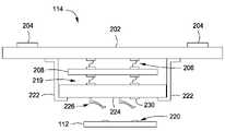
- FIG. 2depicts the probe card assembly 114 according to some embodiments of the invention.
- the probe card assembly 114generally acts as an interface between the test instruments 104 and the DUT 112 .
- the probe card assembly 114can include electrical connectors 204 configured to make electrical connections with a plurality of test channels (not shown) from the test instruments 104 .
- the probe card assembly 114can also include one or more resilient contact elements 226 as test probes.
- the resilient contact elements 226can be configured to be pressed against, and thus make temporary electrical connections with, one or more input and/or output terminals 220 of the DUT 112 .
- the resilient contact elements 226are typically configured to correspond to desired terminals 220 of the DUT 112 and may be arranged in one or more arrays having a desired geometry.
- the probe card assembly 114may include one or more substrates configured to support the connectors 204 and the resilient contact elements 226 and to provide electrical connections therebetween.
- the exemplary probe card assembly 114 shown in FIG. 2has three such substrates, although in other implementations, the probe card assembly 114 can have more or fewer substrates.
- the probe card assembly 114includes interconnect, such as a wiring substrate 202 (also referred to as a printed wiring board), a compliant interposer substrate 208 , and a probe substrate 224 (also referred to as a probe head).
- the wiring substrate 202 , the interposer substrate 208 , and the probe substrate 224can generally be made of any type of suitable material or materials, such as, without limitation, printed circuit boards, ceramics, organic or inorganic materials, and the like, or combinations thereof.
- the probe card assembly 114may include one or more active or passive electronic components (such as capacitors, resistors, and the like).
- one or more ICs 230 having test resourcescan be disposed on the wiring substrate 202 .
- the ICs 230may be disposed on the interposer 408 .
- the ICs 230may be disposed on the probe substrate 224 along with the resilient contact elements 226 .
- the ICs 230can be disposed on any combination of one or more of the wiring substrate 202 , the interposer substrate 208 , and the probe substrate 224 .
- Some electrically conductive pathscan be provided from the connectors 204 through the various substrates to the ICs 230 .
- Other electrically conductive pathscan be provided from the connectors 204 through the various substrates to the resilient contact elements 226 .
- Still other electrically conductive pathscan be provided from the ICs 230 to the resilient contact elements 226 .
- electrically conductive pathsmay be provided from the connectors 204 through the wiring substrate 202 to a plurality of electrically conductive spring interconnect structures 206 .
- Other electrically conductive pathsmay be provided from the spring interconnect structures 206 through the interposer substrate 208 to a plurality of electrically conductive spring interconnect structures 219 .
- Still other electrically conductive pathsmay further be provided from the spring interconnect structures 219 through the probe substrate 224 to the ICs 230 , to the resilient contact elements 226 , or both.
- Still other electrically conductive pathsmay further be provided from the ICs 230 to the resilient contact elements 226 .
- the electrically conductive paths through the wiring substrate 202 , the interposer substrate 208 , and the probe substrate 224can comprise electrically conductive vias, traces, or the like, that may be disposed on, within, and/or through the wiring substrate 202 , the interposer substrate 208 , and the probe substrate 224 .
- the wiring substrate 202 , the interposer substrate 208 , and the probe substrate 224may be held together by one or more brackets 222 and/or other suitable means (such as by bolts, screws, or other suitable fasteners).
- the configuration of the probe card assembly 114 shown in FIG. 2is exemplary only and is simplified for ease of illustration and discussion and many variations, modifications, and additions are contemplated.
- a probe card assemblymay have fewer or more substrates (e.g., 202 , 208 , 224 ) than the probe card assembly 114 shown in FIG. 2 .
- a probe card assemblymay have more than one probe substrate (e.g., 224 ), and each such probe substrate may be independently adjustable.
- Non-limiting examples of probe card assemblies with multiple probe substratesare disclosed in U.S. patent application Ser. No. 11/165,833, filed Jun. 24, 2005. Additional non-limiting examples of probe card assemblies are illustrated in U.S. Pat. No. 5,974,662, issued Nov. 2, 1999 and U.S. Pat. No. 6,509,751, issued Jan. 21, 2003, as well as in the aforementioned U.S. patent application Ser. No. 11/165,833. It is contemplated that various features of the probe card assemblies described in those patents and application may be implemented in the probe card assembly 114 shown in FIG. 2 and that the probe card assemblies described in the aforementioned patents and application may benefit from the use of the inventive intelligent switches and their configurations described herein.
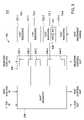
- FIG. 3is a circuit diagram depicting a control group 300 of test resources according to some embodiments of the invention.
- the control group 300may be a portion of a chain of test resources. That is, a chain of test resources may include multiple serially connected instances of the control group 300 .
- the control group 300can include a plurality of test resources 302 (test resources 302 - 1 through 302 - 4 are shown) and control logic 303 .
- the control logic 303may include a shift register 304 and a plurality of shadow registers 306 (shadow registers 306 - 1 through 306 - 5 are shown).
- the shift register 304can include a clock input, a test control input, a clock output, and a test control output.
- the shadow registers 306can include a register control input and a register control output.
- the shift register 304can be a serial in/out, parallel out/in circuit. That is, bits of a test control signal can be serially shifted in the test control input.
- the sequence of bits stored in the shift register 304is referred to herein as a frame.
- a test control inputmay include multiple sequential frames that can be serially shifted through a chain of control groups. Accordingly, bits of the test control signal can be serially shifted out of the test control output of the shift register 304 to another control group.
- the shift register 304can include parallel terminals respectively coupled to the shadow registers 306 .
- a frame stored in the shift register 304can be shifted out in parallel to the shadow registers 306 . Accordingly, a sufficient number of the shadow registers 306 may be provided to store all bits in a frame. Conversely, the contents of the shadow registers 306 may be shifted in parallel into the shift register 304 .
- the shadow registers 306may each include two data ports, which may be bidirectional. One data port of each of the shadow registers 306 can be coupled to one of the parallel terminals of the shift register 304 , as described above. The other data ports of the shadow registers 306 can be coupled to control ports of the test resources 302 . One or more of the shadow registers 306 can be coupled to a respective one or more control ports of a given test resource.
- the shadow register 306 - 1can be coupled to the test resource 302 - 1 .
- the shadow registers 306 - 2 and 306 - 3can be coupled to the test resource 302 - 2 .
- the shadow register 306 - 4can be coupled to the test resource 302 - 3 .
- the shadow register 306 - 5can be coupled to the test resource 302 - 4 .
- the embodiment shown in FIG. 3is one of a myriad of possible embodiments of connections between shadow registers and test resources.
- the test resources 302may include various types of circuits and logic components, such as transistors, logic gates, flip-flops, comparators, operational amplifiers, and the like to provide, at least, the sourcing, sinking, or both of test signals.
- the test resources 302can perform the sourcing, sinking, or both of test signals in response to respective control bits stored in the shadow registers 306 .
- the test resources 302can include different types.
- One or more of the test resources 302may be digital test resources.
- a digital test resourcecan provide a source, sink, or both of a digital test signal in response to a digital control signal.
- test resources 302 - 1 and 302 - 2may be digital test resources configured to receive digital control signals from the shadow registers 306 - 1 , and shadow registers 306 - 2 and 306 - 3 , respectively.
- the test resources 302 - 1 and 302 - 2can source, sink, or both digital test signals (TS- 1 and TS- 2 ).
- test resources 302may be analog test resources.
- An analog test resourcecan provide a source, sink, or both of an analog test signal in response to a digital control signal.
- the test resource 302 - 3may be an analog test resource.
- the test resource 302 - 3may include mixed signal electronics for sourcing, sinking, or both an analog test signal in response to a digital control signal from the shadow register 306 - 4 .
- Such mixed signal electronicscan include a digital-to-analog converter (DAC) 308 , an analog-to-digital converter (ADC) 310 , or both.
- the test resource 302 - 3can source, sink, or both an analog test signal (TS- 3 ).
- test resources 302may be a power test resource.
- a power test resourcecan provide a source of voltage in response to a digital control signal. The source voltage can be received from a power source (e.g., the test instruments) and selectively provided to the DUT in response to a digital control signal.
- the test resource 302 - 4can be a power test resource configured to receive a voltage supply from a test instrument signal and a digital control signal from the shadow register 306 - 5 .
- the test resource 302 - 4can source the voltage supply of the test instrument signal as the test signal (TS- 4 ) in response to the digital control signal from the shadow register 306 - 5 .
- the test resource 302 - 4may include a switch, such as a relay, three-state buffer, of the like capable of switching the voltage supply.
- a switchsuch as a relay, three-state buffer, of the like capable of switching the voltage supply.
- the test resource 302 - 4is described as a power test resource that receives a voltage supply from the test instrument signal, it is to be understood that the test instrument signal can provide other types of resources, such as digital or analog resources. In such case, the test resource 302 - 4 can selectively switch the digital or analog signal in the same manner as the voltage supply signal.
- the types of test resources shown in FIG. 3are merely exemplary, as there are a myriad of possible configurations of digital, analog, and power test resources.
- the test resources 302can be controlled by serially shifting a test control signal into the shift register 304 .
- the test control signalmay be shifted into the shift register 304 in accordance with a clock signal at the clock input.
- the test control signalmay be shifted through the shift register 304 and out the test control output to the next control group in a chain.
- the clock signal at the clock inputmay be provided to the next control group in the chain.
- the test control signalcan be shifted such that a frame is stored in each shift register in a chain. While the test control signal is being shifted through the shift register 304 , the shadow register 306 can be disabled.
- the register control signalcan be used to enable the shadow registers 306 for reading from the shift register 304 , causing the frame stored in the shift register 304 to be parallel shifted into the shadow registers 306 .
- the register control signalcan be used to again disable the shadow registers 306 .
- the register control signalcan be provided to the next control group in a chain.
- the register control signalcan also be used to enable the shadow registers 306 for reading from one or more of the test resources 302 . After transfer, the register control signal can be used to again disable the shadow registers 306 . Then, the shift register 304 can read from the shadow registers 306 in parallel fashion. The contents of the shift register 304 can then be read out serially. Such an operation may be referred to as readback and allows for the capture of test result signals from the DUT.
- FIG. 4is a circuit diagram depicting components on a probe card assembly 114 according to some embodiments of the invention.
- the test instruments 104can include at least one controller 402 .
- the DUT 112can include a set of devices 404 - 1 through 404 -M (generally referred to as devices 404 ), where M is an integer greater than one. That is, the DUT 112 can include multiple test sites (devices to be tested).
- the controller 402may be coupled to one or more ICs 406 for providing one or more test control signals thereto.
- ICs 406 - 1 through 406 -Kare shown, where K is an integer greater than zero.
- Each of the ICs 406can include one or more control groups of test resources, similar to the control group 300 shown in FIG. 3 .
- the ICs 406include test circuits that can have several configurations.
- the ICs 406can include a plurality of ICs serially coupled to form a chain of ICs.
- Each of the ICs 406 in the chainmay include a control group 300 of test resources.
- the IC chainis configured such that the test resource control groups are serially coupled to form a chain of control groups.
- each of the ICs 406includes a plurality of control groups 300 .
- the multiple control groups 300 in a given IC 406may be serially coupled to form a chain, which in turn may be part of a bigger chain.
- the multiple control groups 300 in a given IC 406may be in parallel or may form multiple serially coupled chains in parallel.
- a chain of ICsmay include multiple chains of test resource control groups in parallel.
- only a single IC 406is provided having one or more control groups 300 . In the single IC 406 , multiple control groups may be serially coupled to form a chain, or there may be multiple serially coupled chains of control groups.
- the test resources in the ICs 406may include a first chain and a second chain.
- the first chain of test resourcesmay be responsive to a first test control signal
- the second chain of test resourcesmay be responsive to a second test control signal.
- the first chain of test resourcesmay include digital resources.
- the second chain of test resourcesmay include power resources, analog resources, or both power and analog resources. Having separate chains of test resources for digital and power/analog resources can allow for higher data bandwidth for the digital resources.
- the ICs 406can be in communication with the devices 404 through temporary pressure connections 405 .
- the temporary pressure connectionsmay be effected using test probes, as described above.
- an IC 406may be in communication with one or more of the devices 404 .
- At least one of the test resources in at least one control group 300 in an IC 406may source a test signal to a device 404 through a test probe.
- At least one of the test resources in at least one control group 300 in an IC 406may sink a test signal from a device 404 through a test probe.
- At least one of the test resources in at least one control group 300 in an IC 406may both source and sink test signals to and from a device 404 through at test probe.
- At least one test resource in at least one control group 300 in an IC 406is coupled to receive a test signal from a resource 403 in the test instruments 104 .
- the test instruments 104can generally include a plurality of resources 403 .
- the resources in the test instrumentsmay include any combination of power resources, digital resources, and/or analog resources.
- a test resource in a control group 300may be configured to selectively switch a test signal from a resource 403 in the test instruments 104 .
- some of the test resources (e.g., digital or analog test resources) in the ICs 406can source test signals based on only a test control signal from a controller 402 .
- Others of the test resources (e.g., digital, analog, or power resources) in the ICs 406can source test signals based on both a test signal from a resource 403 and a test control signal from the controller 402 .
- a controller 402can be coupled to a serial input of the IC 406 - 1 through at least one serial interface 410 .
- a serial output of the IC 406 - 1can be coupled to a serial input of the IC 406 - 2
- a serial output of the IC 406 - 2can be coupled to a serial input of the IC 406 - 3 , and so on to form the serial chain that propagates the serial interface(s) 410 .
- the serial interface(s) 410can include a serial interface for each chain of control groups 300 implemented by the ICs 406 .
- the controller 402can also be coupled to the IC 406 - 1 through at least one interface 412 for providing clock and/or other control signals (e.g., register control signal of FIG. 3 ) to the control groups 300 .
- clock and/or other control signalse.g., register control signal of FIG. 3
- one or more serial control linescan be used to control communication of test signals between test resources and the devices 504 in the DUT 112 .
- the number of serial control linesmay be much less than the number of test resources and associated test signals.
- Use of the single control line(s)can substantially reduce the number of routing resources needed on the probe card assembly to control such communication of test signals. This in turn reduces the cost to manufacture the probe card assembly.
- the controller(s) 408may include a plurality of serial interfaces 410 for serially controlling a plurality of IC chains 406 .
- FIG. 5is a flow diagram depicting a process 500 of testing components on a wafer using a probe card assembly according to some embodiments of the invention.
- a test control signalcan be serially shifted through a chain of ICs (block 502 ).
- a frame of the test control signalcan be serially shifted into a shift register in each of the ICs. Bits of the frame can be parallel shifted into shadow registers coupled to a plurality of the test resources.
- Test signalsmay be coupled from test resources to test probes responsive to the test control signal (block 504 ).
- the test signalsinclude at least one digital test signal sourced by at least one digital test resource.
- the test signalsinclude at least one analog test signal sources by at least one analog test resource.
- the test signalsinclude at least one power resource sourced by at least one power test resource.
- the test signalsinclude at least one test signal generated by at least one test resource in the at least one IC.
- the test signalsinclude at least one test signal switched by at least one test resource in the at least one IC.
- a plurality of the test signalsis generated or switched at a plurality of the test resources responsive to bits in shadow registers in each of the ICs.
- test result signalsmay be received at the test resources from the test probes (block 506 ).
- the test resultsmay be digital or analog results received by respective digital or analog test resources.
- captured test result signalsare serially shifted through the chain of ICs and provided as output (e.g., to test instruments) (block 508 ).
- test resourcesmay be included in ICs, which are coupled to form a serial chain of ICs. Each of the test resources may be independently controlled using a serial interface to the chain of ICs. Hence, one or more serial control lines may be used to control a multiplicity of test resources.
- the test resourcesmay include digital resources, analog resources, power resources, or a combination of digital, analog, and/or power resources. Test result data produced by a DUT may be captured by the chain of ICS and read back over the serial interface. This resource-by-resource readback capability can assist in the process of fault isolation among devices under test.
Landscapes
- Engineering & Computer Science (AREA)
- General Engineering & Computer Science (AREA)
- Physics & Mathematics (AREA)
- General Physics & Mathematics (AREA)
- Computer Hardware Design (AREA)
- Microelectronics & Electronic Packaging (AREA)
- Testing Or Measuring Of Semiconductors Or The Like (AREA)
- Measuring Leads Or Probes (AREA)
- Tests Of Electronic Circuits (AREA)
Abstract
Description
- 1. Field of the Invention
- Embodiments of the present invention generally relate to wafer probe cards for testing semiconductor devices and, more specifically, to enhancing the performance of wafer probe cards.
- 2. Description of the Related Art
- Testing is an important step in the production of semiconductor devices for use. Typically, partially or fully completed semiconductor devices may be tested by bringing terminals disposed on an upper surface of a device to be tested—also referred to as a device under test (or DUT)—into contact with resilient contact elements, for example, as contained in a probe card assembly, as part of a test system. A test system controller may be coupled to the probe card assembly to send and receive test signals to and from the DUTs over a set of test channels. A test system controller with increased test channels can be a significant cost factor for a test system. Test system controllers have evolved to increase the number of channels and hence the number of devices that can be tested in parallel (sometimes referred to as multi-site testing). Unfortunately, the number of DUTs per wafer has typically outpaced the development of test system controllers. Conventionally, available channels are typically inadequate for testing all DUTs on a wafer at the same time.
- Some test systems may have common test signals per site in a multi-site test configuration. Common test signals (sometimes referred to as global test signals) are test signals that can be applied to a plurality of DUTs being tested in a single touchdown. One technique to accommodate testing of components on a wafer with a limited number of test channels is to fan out a signal from a test system controller in the probe card assembly to multiple transmission lines. That is, a test signal normally provided to a single DUT can be fanned out to multiple DUTs in the probe card assembly. This technique can enable testing of an increased number of DUTs contemporaneously during a single touchdown for a fixed number of test system channels.
- As the number of DUTs tested in a single touchdown increases, fanning out global signals from the test system controller becomes difficult to implement, if not impractical. The more DUTs that are tested simultaneously, the more fan out lines required on the probe card assembly. Including several thousands of lines on a probe card assembly is undesirable in terms of the required area and complexity of the components of the probe card assembly and in terms of cost.
- Accordingly, there exists a need in the art for a method and apparatus for testing semiconductor devices that attempts to overcome at least some of the aforementioned deficiencies.
- Embodiments of the invention can relate to an apparatus for testing a device under test (DUT). In some embodiments, an apparatus can include an integrated circuit (IC) having a serialized input coupled to test circuits, the test circuits selectively communicating test signals with the DUT responsive to a test control signal on the serialized input.
- Embodiments of the invention can relate to a probe card assembly. In some embodiments, a probe card assembly can include at least one serial control line providing a respective at least one test control signal, and a plurality of integrated circuits (ICs) serially coupled to form a chain, the chain coupled to the at least one serial control line, the plurality of ICs selectively communicating test signals between test resources and test probes responsive to the at least one test control signal.
- Embodiments of the invention can relate to a test assembly. In some embodiments, a test assembly can include a printed wiring board including connectors for connecting to a test system controller, and at least one serial control line providing a respective at least one test control signal from the test system controller; and a probe head supporting test probes and at least one integrated circuit (IC) coupled to the at least one serial control line, the at least one IC selectively communicating test signals between test resources and test probes responsive to the at least one test control signal.
- Embodiments of the invention can relate to a method of testing components on a wafer using a probe card assembly. In some embodiments, a method of testing components on a wafer using a probe card assembly can include serially shifting a test control signal through a chain comprising a plurality of integrated circuits (ICs); selectively coupling test signals from test resources to test probes responsive to the test control signal; capturing test result signals at the test resources from the test probes; and serially reading back from the chain to obtain the test result signals.
- So that the manner in which features of the various embodiments of the present invention can be understood in detail, a more particular description of the invention, briefly summarized above and described more fully below, may be had by reference to embodiments, some of which are illustrated in the appended drawings. It is to be noted, however, that the appended drawings illustrate only typical embodiments of this invention and are therefore not to be considered limiting of its scope, for the invention may admit to other equally effective embodiments.
FIG. 1 is a block diagram depicting a test system according to some embodiments of the invention;FIG. 2 depicts the probe card assembly according to some embodiments of the invention;FIG. 3 is a circuit diagram depicting a control group of test resources according to some embodiments of the invention;FIG. 4 is a circuit diagram depicting components on a probe card assembly according to some embodiments of the invention; andFIG. 5 is a flow diagram depicting a method of testing components on a wafer using a probe card assembly according to embodiments of the invention.- Where possible, identical reference numerals are used herein to designate identical elements that are common to the figures. The images used in the drawings are simplified for illustrative purposes and are not necessarily depicted to scale.
- The present invention provides methods and apparatus for testing devices using serially controlled resources. The resources may be included in ICs, which may be coupled to form one or more serial chains of ICs. The resources in an IC may be of different types. Each of the resources may be independently controlled using one or more serial interfaces to each of ICs. For example, a single serial control line may be used to control a multiplicity of resources, which may be of different types. By serial, it is meant that signals on a serial control line may be transmitted as a sequential bit stream (i.e., transmitted bit-by-bit). The resources may be used as a source of test signals for a plurality of devices, as a sink of test signals from a plurality of devices, or as a source and a sink of test signals. The use of one or more serial control lines to control a multiplicity of resources may substantially reduce the number of conductors required on a probe card assembly. These and other aspects and embodiments of the invention are described in detail below.
FIG. 1 is a block diagram depicting atest system 100 according to some embodiments of the invention. Thetest system 100 can generally include atest system controller 102,test instruments 104, and aprober 106. Thetest system controller 102 can be coupled to thetest instruments 104 by acommunication link 108. Theprober 106 can include astage 110 for mounting a device under test (DUT)112 being tested and aprobe card assembly 114. TheDUT 112 can be any electronic device or devices to be tested. Non-limiting examples of a suitable DUT include one or more dies of an unsingulated semiconductor wafer, one or more semiconductor dies singulated from a wafer (packaged or unpackaged), an array of singulated semiconductor dies disposed in a carrier or other holding device, one or more multi-die electronics modules, one or more printed circuit boards, or any other type of electronic device or devices. The term DUT, as used herein, can refer to one or a plurality of such electronic devices. Theprobe card assembly 114 can include probes116 (also referred to as test probes) that contact theDUT 112. Thestage 110 can be movable to contact theDUT 112 withprobes 116.- The
probe card assembly 114 can includeelectronics 120 for providing a source of test signals to theDUT 112, a sink of test signals from theDUT 112, or both a source and a sink of test signals to and from theDUT 112. A source or sink of a test signal may be referred to herein as a test resource or resource. In some embodiments, theelectronics 120 can include one or more chains of test resources. Each chain of test resources is controlled serially using a serial control signal referred to herein as a test control signal. Note the difference between a test signal and a test control signal. A test signal is a signal ultimately applied to theDUT 112 for purposes of testing or a signal received from theDUT 112 in response to testing. A test control signal is a signal that controls some test resources in theelectronics 120 to provide a source or a sink of test signals. The chain(s) of test resources may be implemented using one or more chains of ICs. Aspects of the test resources and IC implementations thereof are described below. - In the
test system 100, test signals can be transmitted by theelectronics 120 to theDUT 112 through theprobes 116. Test signals can be received by the electronics from theDUT 112 through theprobes 116. The transmission and/or reception of test signals by theelectronics 120 may be controlled by thetest instruments 104. Some of the test resources in theelectronics 120 can generate test signals (e.g., digital or analog data signals) in response to one or more test control signals, which are provided by thetest instruments 104. Thetest instruments 104 can also generate test signals (e.g., supply voltage signals), which are in turn coupled to theelectronics 120. Others of the test resources can provide a controllable source of these test signals generated by thetest instruments 104 in response to one or more test control signals, which may also be provided by thetest instruments 104. Thetest instruments 104 can also generate test signals, which are, in turn, coupled directly to some of the probes116 (e.g., bypassing the electronics120). - The
test instruments 104 may be controlled by the test system controller102 (e.g., a general purpose computer). Test signals received by theelectronics 120 from theDUT 112 may be referred to as test results. Test results can be provided from theelectronics 120 to thetest instruments 104. Thetest instruments 104 may transmit the test results to thetest system controller 102 for analysis. - The
test instruments 104 may be linked byconnectors 118 to theprobe card assembly 114. The links provided by theconnectors 118 can be divided into individual test channels. The test channels may be used to convey test control signals or test signals (including test results). Theconnectors 118 may be any suitable connectors, such as flexible cable connectors, pogo pins, zero insertion force (ZIF) connectors, or the like. Theprobe card assembly 114 can fan out one or more of the test channels such that the signal conveyed therein can be coupled to multiple components. FIG. 2 depicts theprobe card assembly 114 according to some embodiments of the invention. Theprobe card assembly 114 generally acts as an interface between thetest instruments 104 and theDUT 112. Theprobe card assembly 114 can includeelectrical connectors 204 configured to make electrical connections with a plurality of test channels (not shown) from thetest instruments 104. Theprobe card assembly 114 can also include one or moreresilient contact elements 226 as test probes. Theresilient contact elements 226 can be configured to be pressed against, and thus make temporary electrical connections with, one or more input and/oroutput terminals 220 of theDUT 112. Theresilient contact elements 226 are typically configured to correspond to desiredterminals 220 of theDUT 112 and may be arranged in one or more arrays having a desired geometry.- The
probe card assembly 114 may include one or more substrates configured to support theconnectors 204 and theresilient contact elements 226 and to provide electrical connections therebetween. The exemplaryprobe card assembly 114 shown inFIG. 2 has three such substrates, although in other implementations, theprobe card assembly 114 can have more or fewer substrates. In the embodiment depicted inFIG. 2 , theprobe card assembly 114 includes interconnect, such as a wiring substrate202 (also referred to as a printed wiring board), acompliant interposer substrate 208, and a probe substrate224 (also referred to as a probe head). Thewiring substrate 202, theinterposer substrate 208, and theprobe substrate 224 can generally be made of any type of suitable material or materials, such as, without limitation, printed circuit boards, ceramics, organic or inorganic materials, and the like, or combinations thereof. - Additionally, the
probe card assembly 114 may include one or more active or passive electronic components (such as capacitors, resistors, and the like). In some embodiments, one ormore ICs 230 having test resources can be disposed on thewiring substrate 202. In other embodiments, theICs 230 may be disposed on the interposer408. In still other embodiments, theICs 230 may be disposed on theprobe substrate 224 along with theresilient contact elements 226. In other embodiments, theICs 230 can be disposed on any combination of one or more of thewiring substrate 202, theinterposer substrate 208, and theprobe substrate 224. - Some electrically conductive paths (not shown) can be provided from the
connectors 204 through the various substrates to theICs 230. Other electrically conductive paths (not shown) can be provided from theconnectors 204 through the various substrates to theresilient contact elements 226. Still other electrically conductive paths (not shown) can be provided from theICs 230 to theresilient contact elements 226. - For example, in the embodiment depicted in
FIG. 2 , electrically conductive paths (not shown) may be provided from theconnectors 204 through thewiring substrate 202 to a plurality of electrically conductivespring interconnect structures 206. Other electrically conductive paths (not shown) may be provided from thespring interconnect structures 206 through theinterposer substrate 208 to a plurality of electrically conductivespring interconnect structures 219. Still other electrically conductive paths (not shown) may further be provided from thespring interconnect structures 219 through theprobe substrate 224 to theICs 230, to theresilient contact elements 226, or both. Still other electrically conductive paths (not shown) may further be provided from theICs 230 to theresilient contact elements 226. The electrically conductive paths through thewiring substrate 202, theinterposer substrate 208, and theprobe substrate 224 can comprise electrically conductive vias, traces, or the like, that may be disposed on, within, and/or through thewiring substrate 202, theinterposer substrate 208, and theprobe substrate 224. - The
wiring substrate 202, theinterposer substrate 208, and theprobe substrate 224 may be held together by one ormore brackets 222 and/or other suitable means (such as by bolts, screws, or other suitable fasteners). The configuration of theprobe card assembly 114 shown inFIG. 2 is exemplary only and is simplified for ease of illustration and discussion and many variations, modifications, and additions are contemplated. For example, a probe card assembly may have fewer or more substrates (e.g.,202,208,224) than theprobe card assembly 114 shown inFIG. 2 . As another example, a probe card assembly may have more than one probe substrate (e.g.,224), and each such probe substrate may be independently adjustable. Non-limiting examples of probe card assemblies with multiple probe substrates are disclosed in U.S. patent application Ser. No. 11/165,833, filed Jun. 24, 2005. Additional non-limiting examples of probe card assemblies are illustrated in U.S. Pat. No. 5,974,662, issued Nov. 2, 1999 and U.S. Pat. No. 6,509,751, issued Jan. 21, 2003, as well as in the aforementioned U.S. patent application Ser. No. 11/165,833. It is contemplated that various features of the probe card assemblies described in those patents and application may be implemented in theprobe card assembly 114 shown inFIG. 2 and that the probe card assemblies described in the aforementioned patents and application may benefit from the use of the inventive intelligent switches and their configurations described herein. FIG. 3 is a circuit diagram depicting acontrol group 300 of test resources according to some embodiments of the invention. Thecontrol group 300 may be a portion of a chain of test resources. That is, a chain of test resources may include multiple serially connected instances of thecontrol group 300. Thecontrol group 300 can include a plurality of test resources302 (test resources302-1 through302-4 are shown) andcontrol logic 303. Thecontrol logic 303 may include ashift register 304 and a plurality of shadow registers306 (shadow registers306-1 through306-5 are shown). Theshift register 304 can include a clock input, a test control input, a clock output, and a test control output. The shadow registers306 can include a register control input and a register control output.- The
shift register 304 can be a serial in/out, parallel out/in circuit. That is, bits of a test control signal can be serially shifted in the test control input. The sequence of bits stored in theshift register 304 is referred to herein as a frame. A test control input may include multiple sequential frames that can be serially shifted through a chain of control groups. Accordingly, bits of the test control signal can be serially shifted out of the test control output of theshift register 304 to another control group. Theshift register 304 can include parallel terminals respectively coupled to the shadow registers306. A frame stored in theshift register 304 can be shifted out in parallel to the shadow registers306. Accordingly, a sufficient number of the shadow registers306 may be provided to store all bits in a frame. Conversely, the contents of the shadow registers306 may be shifted in parallel into theshift register 304. - The shadow registers306 may each include two data ports, which may be bidirectional. One data port of each of the shadow registers306 can be coupled to one of the parallel terminals of the
shift register 304, as described above. The other data ports of the shadow registers306 can be coupled to control ports of the test resources302. One or more of the shadow registers306 can be coupled to a respective one or more control ports of a given test resource. For example, the shadow register306-1 can be coupled to the test resource302-1. The shadow registers306-2 and306-3 can be coupled to the test resource302-2. The shadow register306-4 can be coupled to the test resource302-3. The shadow register306-5 can be coupled to the test resource302-4. The embodiment shown inFIG. 3 is one of a myriad of possible embodiments of connections between shadow registers and test resources. - The test resources302 may include various types of circuits and logic components, such as transistors, logic gates, flip-flops, comparators, operational amplifiers, and the like to provide, at least, the sourcing, sinking, or both of test signals. The test resources302 can perform the sourcing, sinking, or both of test signals in response to respective control bits stored in the shadow registers306. The test resources302 can include different types. One or more of the test resources302 may be digital test resources. A digital test resource can provide a source, sink, or both of a digital test signal in response to a digital control signal. For example, the test resources302-1 and302-2 may be digital test resources configured to receive digital control signals from the shadow registers306-1, and shadow registers306-2 and306-3, respectively. The test resources302-1 and302-2 can source, sink, or both digital test signals (TS-1 and TS-2).
- One or more of the test resources302 may be analog test resources. An analog test resource can provide a source, sink, or both of an analog test signal in response to a digital control signal. For example, the test resource302-3 may be an analog test resource. The test resource302-3 may include mixed signal electronics for sourcing, sinking, or both an analog test signal in response to a digital control signal from the shadow register306-4. Such mixed signal electronics can include a digital-to-analog converter (DAC)308, an analog-to-digital converter (ADC)310, or both. The test resource302-3 can source, sink, or both an analog test signal (TS-3).
- One or more of the test resources302 may be a power test resource. A power test resource can provide a source of voltage in response to a digital control signal. The source voltage can be received from a power source (e.g., the test instruments) and selectively provided to the DUT in response to a digital control signal. For example, the test resource302-4 can be a power test resource configured to receive a voltage supply from a test instrument signal and a digital control signal from the shadow register306-5. The test resource302-4 can source the voltage supply of the test instrument signal as the test signal (TS-4) in response to the digital control signal from the shadow register306-5. For example, the test resource302-4 may include a switch, such as a relay, three-state buffer, of the like capable of switching the voltage supply. Although the test resource302-4 is described as a power test resource that receives a voltage supply from the test instrument signal, it is to be understood that the test instrument signal can provide other types of resources, such as digital or analog resources. In such case, the test resource302-4 can selectively switch the digital or analog signal in the same manner as the voltage supply signal. The types of test resources shown in
FIG. 3 are merely exemplary, as there are a myriad of possible configurations of digital, analog, and power test resources. - In operation, the test resources302 can be controlled by serially shifting a test control signal into the
shift register 304. The test control signal may be shifted into theshift register 304 in accordance with a clock signal at the clock input. The test control signal may be shifted through theshift register 304 and out the test control output to the next control group in a chain. The clock signal at the clock input may be provided to the next control group in the chain. The test control signal can be shifted such that a frame is stored in each shift register in a chain. While the test control signal is being shifted through theshift register 304, theshadow register 306 can be disabled. When shifting is complete, the register control signal can be used to enable the shadow registers306 for reading from theshift register 304, causing the frame stored in theshift register 304 to be parallel shifted into the shadow registers306. After transfer, the register control signal can be used to again disable the shadow registers306. The register control signal can be provided to the next control group in a chain. - The register control signal can also be used to enable the shadow registers306 for reading from one or more of the test resources302. After transfer, the register control signal can be used to again disable the shadow registers306. Then, the
shift register 304 can read from the shadow registers306 in parallel fashion. The contents of theshift register 304 can then be read out serially. Such an operation may be referred to as readback and allows for the capture of test result signals from the DUT. FIG. 4 is a circuit diagram depicting components on aprobe card assembly 114 according to some embodiments of the invention. Thetest instruments 104 can include at least onecontroller 402. In the example shown, theDUT 112 can include a set of devices404-1 through404-M (generally referred to as devices404), where M is an integer greater than one. That is, theDUT 112 can include multiple test sites (devices to be tested).- The
controller 402 may be coupled to one or more ICs406 for providing one or more test control signals thereto. In the present example, ICs406-1 through406-K are shown, where K is an integer greater than zero. Each of the ICs406 can include one or more control groups of test resources, similar to thecontrol group 300 shown inFIG. 3 . The ICs406 include test circuits that can have several configurations. In some embodiments, the ICs406 can include a plurality of ICs serially coupled to form a chain of ICs. Each of the ICs406 in the chain may include acontrol group 300 of test resources. The IC chain is configured such that the test resource control groups are serially coupled to form a chain of control groups. In some embodiments, each of the ICs406 includes a plurality ofcontrol groups 300. Themultiple control groups 300 in a given IC406 may be serially coupled to form a chain, which in turn may be part of a bigger chain. Themultiple control groups 300 in a given IC406 may be in parallel or may form multiple serially coupled chains in parallel. Thus, a chain of ICs may include multiple chains of test resource control groups in parallel. In some embodiments, only a single IC406 is provided having one ormore control groups 300. In the single IC406, multiple control groups may be serially coupled to form a chain, or there may be multiple serially coupled chains of control groups. - In some embodiments, the test resources in the ICs406 may include a first chain and a second chain. The first chain of test resources may be responsive to a first test control signal, and the second chain of test resources may be responsive to a second test control signal. The first chain of test resources may include digital resources. The second chain of test resources may include power resources, analog resources, or both power and analog resources. Having separate chains of test resources for digital and power/analog resources can allow for higher data bandwidth for the digital resources.
- The ICs406 can be in communication with the
devices 404 throughtemporary pressure connections 405. The temporary pressure connections may be effected using test probes, as described above. In some embodiments, there may be an IC406 for each of thedevices 404. In some embodiments, an IC406 may be in communication with one or more of thedevices 404. At least one of the test resources in at least onecontrol group 300 in an IC406 may source a test signal to adevice 404 through a test probe. At least one of the test resources in at least onecontrol group 300 in an IC406 may sink a test signal from adevice 404 through a test probe. At least one of the test resources in at least onecontrol group 300 in an IC406 may both source and sink test signals to and from adevice 404 through at test probe. - In some embodiments, at least one test resource in at least one
control group 300 in an IC406 is coupled to receive a test signal from aresource 403 in thetest instruments 104. Thetest instruments 104 can generally include a plurality ofresources 403. The resources in the test instruments may include any combination of power resources, digital resources, and/or analog resources. A test resource in acontrol group 300 may be configured to selectively switch a test signal from aresource 403 in thetest instruments 104. Accordingly, some of the test resources (e.g., digital or analog test resources) in the ICs406 can source test signals based on only a test control signal from acontroller 402. Others of the test resources (e.g., digital, analog, or power resources) in the ICs406 can source test signals based on both a test signal from aresource 403 and a test control signal from thecontroller 402. - A
controller 402 can be coupled to a serial input of the IC406-1 through at least oneserial interface 410. In case multiple ICs406 are present, a serial output of the IC406-1 can be coupled to a serial input of the IC406-2, a serial output of the IC406-2 can be coupled to a serial input of the IC406-3, and so on to form the serial chain that propagates the serial interface(s)410. The serial interface(s)410 can include a serial interface for each chain ofcontrol groups 300 implemented by the ICs406. Thecontroller 402 can also be coupled to the IC406-1 through at least oneinterface 412 for providing clock and/or other control signals (e.g., register control signal ofFIG. 3 ) to thecontrol groups 300. Thus one or more serial control lines can be used to control communication of test signals between test resources and thedevices 504 in theDUT 112. The number of serial control lines may be much less than the number of test resources and associated test signals. Use of the single control line(s) can substantially reduce the number of routing resources needed on the probe card assembly to control such communication of test signals. This in turn reduces the cost to manufacture the probe card assembly. - In the present example, a single chain of ICs406 is shown. In some embodiments, multiple chains of ICs may be provided. In such embodiments, the controller(s)408 may include a plurality of
serial interfaces 410 for serially controlling a plurality of IC chains406. FIG. 5 is a flow diagram depicting aprocess 500 of testing components on a wafer using a probe card assembly according to some embodiments of the invention. In theprocess 500, a test control signal can be serially shifted through a chain of ICs (block502). In some embodiments, a frame of the test control signal can be serially shifted into a shift register in each of the ICs. Bits of the frame can be parallel shifted into shadow registers coupled to a plurality of the test resources.- Test signals may be coupled from test resources to test probes responsive to the test control signal (block504). In some embodiments, the test signals include at least one digital test signal sourced by at least one digital test resource. In some embodiments, the test signals include at least one analog test signal sources by at least one analog test resource. In some embodiments, the test signals include at least one power resource sourced by at least one power test resource. In some embodiments, the test signals include at least one test signal generated by at least one test resource in the at least one IC. In some embodiments, the test signals include at least one test signal switched by at least one test resource in the at least one IC. In some embodiments, a plurality of the test signals is generated or switched at a plurality of the test resources responsive to bits in shadow registers in each of the ICs.
- In some embodiments, test result signals may be received at the test resources from the test probes (block506). The test results may be digital or analog results received by respective digital or analog test resources. In some embodiments, captured test result signals are serially shifted through the chain of ICs and provided as output (e.g., to test instruments) (block508).
- Thus, methods and apparatus for testing devices using serially controlled test resources have been described. The test resources may be included in ICs, which are coupled to form a serial chain of ICs. Each of the test resources may be independently controlled using a serial interface to the chain of ICs. Hence, one or more serial control lines may be used to control a multiplicity of test resources. The test resources may include digital resources, analog resources, power resources, or a combination of digital, analog, and/or power resources. Test result data produced by a DUT may be captured by the chain of ICS and read back over the serial interface. This resource-by-resource readback capability can assist in the process of fault isolation among devices under test.
- While the foregoing is directed to embodiments of the present invention, other and further embodiments of the invention may be devised without departing from the basic scope thereof, and the scope thereof is determined by the claims that follow.
Claims (21)
Priority Applications (8)
| Application Number | Priority Date | Filing Date | Title |
|---|---|---|---|
| US11/861,223US7888955B2 (en) | 2007-09-25 | 2007-09-25 | Method and apparatus for testing devices using serially controlled resources |
| EP08833524AEP2195673A1 (en) | 2007-09-25 | 2008-09-24 | Method and apparatus for testing devices using serially controlled resources |
| TW097136656ATWI425223B (en) | 2007-09-25 | 2008-09-24 | Method and apparatus for testing devices using serially controlled resources |
| JP2010526068AJP5859204B2 (en) | 2007-09-25 | 2008-09-24 | Device for verifying a device using serially controlled resources |
| KR1020107008977AKR20100075546A (en) | 2007-09-25 | 2008-09-24 | Method and apparatus for testing devices using serially controlled resources |
| PCT/US2008/077585WO2009042730A1 (en) | 2007-09-25 | 2008-09-24 | Method and apparatus for testing devices using serially controlled resources |
| CN200880115433ACN101855562A (en) | 2007-09-25 | 2008-09-24 | Method and apparatus for testing devices using serially controlled resources |
| JP2015187934AJP6185969B2 (en) | 2007-09-25 | 2015-09-25 | Method and apparatus for testing a device using serially controlled resources |
Applications Claiming Priority (1)
| Application Number | Priority Date | Filing Date | Title |
|---|---|---|---|
| US11/861,223US7888955B2 (en) | 2007-09-25 | 2007-09-25 | Method and apparatus for testing devices using serially controlled resources |
Publications (2)
| Publication Number | Publication Date |
|---|---|
| US20090079448A1true US20090079448A1 (en) | 2009-03-26 |
| US7888955B2 US7888955B2 (en) | 2011-02-15 |
Family
ID=40470956
Family Applications (1)
| Application Number | Title | Priority Date | Filing Date |
|---|---|---|---|
| US11/861,223Expired - Fee RelatedUS7888955B2 (en) | 2007-09-25 | 2007-09-25 | Method and apparatus for testing devices using serially controlled resources |
Country Status (7)
| Country | Link |
|---|---|
| US (1) | US7888955B2 (en) |
| EP (1) | EP2195673A1 (en) |
| JP (2) | JP5859204B2 (en) |
| KR (1) | KR20100075546A (en) |
| CN (1) | CN101855562A (en) |
| TW (1) | TWI425223B (en) |
| WO (1) | WO2009042730A1 (en) |
Cited By (4)
| Publication number | Priority date | Publication date | Assignee | Title |
|---|---|---|---|---|
| US20110043233A1 (en)* | 2009-08-18 | 2011-02-24 | Formfactor, Inc. | Wafer level contactor |
| US20120081137A1 (en)* | 2010-10-05 | 2012-04-05 | Stmicroelectronics S.R.L. | Testing method for semiconductor integrated electronic devices and corresponding test architecture |
| CN106940424A (en)* | 2016-01-05 | 2017-07-11 | 德律科技股份有限公司 | Multi-chassis testing device and testing signal transmission device thereof |
| US20180017620A1 (en)* | 2015-04-01 | 2018-01-18 | Advantest Corporation | Method for operating a test apparatus and a test apparatus |
Families Citing this family (3)
| Publication number | Priority date | Publication date | Assignee | Title |
|---|---|---|---|---|
| DE102005037236A1 (en)* | 2005-08-08 | 2007-02-15 | Robert Bosch Gmbh | Device and method for configuring a semiconductor circuit |
| CN109863413B (en) | 2016-05-20 | 2022-03-25 | 默升科技集团有限公司 | Scan-based test design in SERDES applications |
| CN108333395A (en)* | 2018-03-29 | 2018-07-27 | 无锡品测科技有限公司 | A kind of probe card substrate based on wafer test design |
Citations (67)
| Publication number | Priority date | Publication date | Assignee | Title |
|---|---|---|---|---|
| US3781683A (en)* | 1971-03-30 | 1973-12-25 | Ibm | Test circuit configuration for integrated semiconductor circuits and a test system containing said configuration |
| US3827820A (en)* | 1971-08-20 | 1974-08-06 | J Hoffman | Drill dispensing container |
| US4038599A (en)* | 1974-12-30 | 1977-07-26 | International Business Machines Corporation | High density wafer contacting and test system |
| US4455654A (en)* | 1981-06-05 | 1984-06-19 | John Fluke Mfg. Co., Inc. | Test apparatus for electronic assemblies employing a microprocessor |
| US4465972A (en)* | 1982-04-05 | 1984-08-14 | Allied Corporation | Connection arrangement for printed circuit board testing apparatus |
| US4468616A (en)* | 1980-08-29 | 1984-08-28 | Fujitsu Limited | Testing equipment for electric components |
| US4523144A (en)* | 1980-05-27 | 1985-06-11 | Japan Electronic Materials Corp. | Complex probe card for testing a semiconductor wafer |
| US4706018A (en)* | 1984-11-01 | 1987-11-10 | International Business Machines Corporation | Noncontact dynamic tester for integrated circuits |
| US4780670A (en)* | 1985-03-04 | 1988-10-25 | Xerox Corporation | Active probe card for high resolution/low noise wafer level testing |
| US4837622A (en)* | 1985-05-10 | 1989-06-06 | Micro-Probe, Inc. | High density probe card |
| US4899099A (en)* | 1988-05-19 | 1990-02-06 | Augat Inc. | Flex dot wafer probe |
| US5070297A (en)* | 1990-06-04 | 1991-12-03 | Texas Instruments Incorporated | Full wafer integrated circuit testing device |
| US5090118A (en)* | 1990-07-31 | 1992-02-25 | Texas Instruments Incorporated | High performance test head and method of making |
| US5103557A (en)* | 1988-05-16 | 1992-04-14 | Leedy Glenn J | Making and testing an integrated circuit using high density probe points |
| US5148103A (en)* | 1990-10-31 | 1992-09-15 | Hughes Aircraft Company | Apparatus for testing integrated circuits |
| US5162728A (en)* | 1990-09-11 | 1992-11-10 | Cray Computer Corporation | Functional at speed test system for integrated circuits on undiced wafers |
| US5172050A (en)* | 1991-02-15 | 1992-12-15 | Motorola, Inc. | Micromachined semiconductor probe card |
| US5187020A (en)* | 1990-07-31 | 1993-02-16 | Texas Instruments Incorporated | Compliant contact pad |
| US5191708A (en)* | 1990-06-20 | 1993-03-09 | Hitachi, Ltd. | Manufacturing method of a probe head for semiconductor LSI inspection apparatus |
| US5243274A (en)* | 1992-08-07 | 1993-09-07 | Westinghouse Electric Corp. | Asic tester |
| US5261155A (en)* | 1991-08-12 | 1993-11-16 | International Business Machines Corporation | Method for bonding flexible circuit to circuitized substrate to provide electrical connection therebetween using different solders |
| US5323107A (en)* | 1991-04-15 | 1994-06-21 | Hitachi America, Ltd. | Active probe card |
| US5357523A (en)* | 1991-12-18 | 1994-10-18 | International Business Machines Corporation | Memory testing system with algorithmic test data generation |
| US5363038A (en)* | 1992-08-12 | 1994-11-08 | Fujitsu Limited | Method and apparatus for testing an unpopulated chip carrier using a module test card |
| US5367254A (en)* | 1993-02-01 | 1994-11-22 | International Business Machines Corporation | Test probe assembly using buckling wire probes within tubes having opposed overlapping slots |
| US5389556A (en)* | 1992-07-02 | 1995-02-14 | Lsi Logic Corporation | Individually powering-up unsingulated dies on a wafer |
| US5406210A (en)* | 1992-02-07 | 1995-04-11 | Gec-Marconi Limited | Apparatus and method for testing bare dies with low contact resistance between the die and testing station |
| US5422574A (en)* | 1993-01-14 | 1995-06-06 | Probe Technology Corporation | Large scale protrusion membrane for semiconductor devices under test with very high pin counts |
| US5434513A (en)* | 1992-08-10 | 1995-07-18 | Rohm Co., Ltd. | Semiconductor wafer testing apparatus using intermediate semiconductor wafer |
| US5442282A (en)* | 1992-07-02 | 1995-08-15 | Lsi Logic Corporation | Testing and exercising individual, unsingulated dies on a wafer |
| US5476211A (en)* | 1993-11-16 | 1995-12-19 | Form Factor, Inc. | Method of manufacturing electrical contacts, using a sacrificial member |
| US5479105A (en)* | 1993-06-25 | 1995-12-26 | Samsung Electronics Co., Ltd. | Known-good die testing apparatus |
| US5491426A (en)* | 1994-06-30 | 1996-02-13 | Vlsi Technology, Inc. | Adaptable wafer probe assembly for testing ICs with different power/ground bond pad configurations |
| US5495667A (en)* | 1994-11-07 | 1996-03-05 | Micron Technology, Inc. | Method for forming contact pins for semiconductor dice and interconnects |
| US5497079A (en)* | 1992-09-01 | 1996-03-05 | Matsushita Electric Industrial Co., Ltd. | Semiconductor testing apparatus, semiconductor testing circuit chip, and probe card |
| US5532610A (en)* | 1993-08-25 | 1996-07-02 | Nec Corporation | Apparatus for testing semicondctor wafer |
| US5534784A (en)* | 1994-05-02 | 1996-07-09 | Motorola, Inc. | Method for probing a semiconductor wafer |
| US5541505A (en)* | 1991-05-15 | 1996-07-30 | Mega Chips Corporation | Testing integrated circuits by consolidating a plurality of digital signals as a multilevel signal |
| US5568054A (en)* | 1992-07-31 | 1996-10-22 | Tokyo Electron Limited | Probe apparatus having burn-in test function |
| US5570032A (en)* | 1993-08-17 | 1996-10-29 | Micron Technology, Inc. | Wafer scale burn-in apparatus and process |
| US5600257A (en)* | 1995-08-09 | 1997-02-04 | International Business Machines Corporation | Semiconductor wafer test and burn-in |
| US5625297A (en)* | 1989-04-26 | 1997-04-29 | Atg Electronic Gmbh | Testing device for testing electrical or electronic test specimens |
| US5642054A (en)* | 1995-08-08 | 1997-06-24 | Hughes Aircraft Company | Active circuit multi-port membrane probe for full wafer testing |
| US5648661A (en)* | 1992-07-02 | 1997-07-15 | Lsi Logic Corporation | Integrated circuit wafer comprising unsingulated dies, and decoder arrangement for individually testing the dies |
| US5669774A (en)* | 1994-09-06 | 1997-09-23 | Grabbe; Dimitry | Ball grid array socket |
| US5670889A (en)* | 1994-10-17 | 1997-09-23 | Nihon Denshizairyo Kabushiki Kaisha | Probe card for maintaining the position of a probe in high temperature application |
| US5686842A (en)* | 1995-08-31 | 1997-11-11 | Nat Semiconductor Corp | Known good die test apparatus and method |
| US5701085A (en)* | 1995-07-05 | 1997-12-23 | Sun Microsystems, Inc. | Apparatus for testing flip chip or wire bond integrated circuits |
| US5701666A (en)* | 1994-08-31 | 1997-12-30 | Motorola, Inc. | Method for manufacturing a stimulus wafer for use in a wafer-to-wafer testing system to test integrated circuits located on a product wafer |
| US5736850A (en)* | 1995-09-11 | 1998-04-07 | Teradyne, Inc. | Configurable probe card for automatic test equipment |
| US5764072A (en)* | 1996-12-20 | 1998-06-09 | Probe Technology | Dual contact probe assembly for testing integrated circuits |
| US6064213A (en)* | 1993-11-16 | 2000-05-16 | Formfactor, Inc. | Wafer-level burn-in and test |
| US6275051B1 (en)* | 1997-12-29 | 2001-08-14 | International Business Machines Corporation | Segmented architecture for wafer test and burn-in |
| US6400173B1 (en)* | 1999-11-19 | 2002-06-04 | Hitachi, Ltd. | Test system and manufacturing of semiconductor device |
| US6500257B1 (en)* | 1998-04-17 | 2002-12-31 | Agilent Technologies, Inc. | Epitaxial material grown laterally within a trench and method for producing same |
| US6525555B1 (en)* | 1993-11-16 | 2003-02-25 | Formfactor, Inc. | Wafer-level burn-in and test |
| US6649931B2 (en)* | 2000-11-22 | 2003-11-18 | Hitachi, Ltd. | Semiconductor wafer, semiconductor chip, semiconductor device and method for manufacturing semiconductor device |
| US6691055B2 (en)* | 1999-12-23 | 2004-02-10 | Em Microelectronic-Marin Sa | Integrated circuit provided with means for calibrating an electronic module and method for calibrating an electronic module of an integrated circuit |
| US20040068869A1 (en)* | 1993-11-16 | 2004-04-15 | Formfactor, Inc. | Mounting spring elements on semiconductor devices, and wafer-level testing methodology |
| US20040117705A1 (en)* | 2002-05-14 | 2004-06-17 | Zounes Thomas David | Method and system for disabling a scanout line of a register flip-flop |
| US6781908B1 (en)* | 2003-02-19 | 2004-08-24 | Freescale Semiconductor, Inc. | Memory having variable refresh control and method therefor |
| US6856150B2 (en)* | 2001-04-10 | 2005-02-15 | Formfactor, Inc. | Probe card with coplanar daughter card |
| US20060273809A1 (en)* | 2004-04-21 | 2006-12-07 | Formfactor, Inc. | Method of designing an application specific probe card test system |
| US7245134B2 (en)* | 2005-01-31 | 2007-07-17 | Formfactor, Inc. | Probe card assembly including a programmable device to selectively route signals from channels of a test system controller to probes |
| US7307433B2 (en)* | 2004-04-21 | 2007-12-11 | Formfactor, Inc. | Intelligent probe card architecture |
| US20090085590A1 (en)* | 2007-09-27 | 2009-04-02 | Formfactor, Inc. | Method And Apparatus For Testing Devices Using Serially Controlled Intelligent Switches |
| US7750652B2 (en)* | 2006-06-12 | 2010-07-06 | Cascade Microtech, Inc. | Test structure and probe for differential signals |
Family Cites Families (32)
| Publication number | Priority date | Publication date | Assignee | Title |
|---|---|---|---|---|
| US5917707A (en) | 1993-11-16 | 1999-06-29 | Formfactor, Inc. | Flexible contact structure with an electrically conductive shell |
| JPS63111479A (en)* | 1986-10-29 | 1988-05-16 | Hitachi Electronics Eng Co Ltd | Ic testing device |
| JP2660028B2 (en) | 1988-12-13 | 1997-10-08 | 株式会社東芝 | LSI test equipment |
| JPH02237047A (en)* | 1989-03-09 | 1990-09-19 | Mitsubishi Electric Corp | Semiconductor testing device |
| FR2645679B1 (en) | 1989-04-07 | 1994-05-06 | Onera (Off Nat Aerospatiale) | TEST INSTALLATION, PARTICULARLY FOR SEMICONDUCTOR MATERIAL WAFERS |
| DE9004562U1 (en) | 1989-04-26 | 1990-07-19 | atg electronic GmbH i.K., 97877 Wertheim | Test device for testing electrical or electronic test objects |
| US6219908B1 (en) | 1991-06-04 | 2001-04-24 | Micron Technology, Inc. | Method and apparatus for manufacturing known good semiconductor die |
| US5371654A (en) | 1992-10-19 | 1994-12-06 | International Business Machines Corporation | Three dimensional high performance interconnection package |
| JPH06180342A (en) | 1992-12-14 | 1994-06-28 | Ono Sokki Co Ltd | Ic evaluating device |
| US5832601A (en) | 1993-11-16 | 1998-11-10 | Form Factor, Inc. | Method of making temporary connections between electronic components |
| US6336269B1 (en) | 1993-11-16 | 2002-01-08 | Benjamin N. Eldridge | Method of fabricating an interconnection element |
| US5897326A (en) | 1993-11-16 | 1999-04-27 | Eldridge; Benjamin N. | Method of exercising semiconductor devices |
| US5983493A (en) | 1993-11-16 | 1999-11-16 | Formfactor, Inc. | Method of temporarily, then permanently, connecting to a semiconductor device |
| US5772451A (en) | 1993-11-16 | 1998-06-30 | Form Factor, Inc. | Sockets for electronic components and methods of connecting to electronic components |
| US5806181A (en) | 1993-11-16 | 1998-09-15 | Formfactor, Inc. | Contact carriers (tiles) for populating larger substrates with spring contacts |
| US5974662A (en) | 1993-11-16 | 1999-11-02 | Formfactor, Inc. | Method of planarizing tips of probe elements of a probe card assembly |
| US6029344A (en) | 1993-11-16 | 2000-02-29 | Formfactor, Inc. | Composite interconnection element for microelectronic components, and method of making same |
| US5878486A (en) | 1993-11-16 | 1999-03-09 | Formfactor, Inc. | Method of burning-in semiconductor devices |
| JP2621785B2 (en)* | 1994-01-26 | 1997-06-18 | 三菱電機株式会社 | Semiconductor test equipment |
| JP3443947B2 (en) | 1994-07-22 | 2003-09-08 | 株式会社デンソー | Burn-in dedicated wafer and burn-in method using the same |
| JP2725615B2 (en)* | 1994-10-31 | 1998-03-11 | 日本電気株式会社 | Integrated circuit test equipment |
| US6133744A (en) | 1995-04-28 | 2000-10-17 | Nec Corporation | Apparatus for testing semiconductor wafer |
| US5834946A (en) | 1995-10-19 | 1998-11-10 | Mosaid Technologies Incorporated | Integrated circuit test head |
| JP3838381B2 (en) | 1995-11-22 | 2006-10-25 | 株式会社アドバンテスト | Probe card |
| US6059982A (en) | 1997-09-30 | 2000-05-09 | International Business Machines Corporation | Micro probe assembly and method of fabrication |
| US6316988B1 (en) | 1999-03-26 | 2001-11-13 | Seagate Technology Llc | Voltage margin testing using an embedded programmable voltage source |
| FR2792798B1 (en) | 1999-04-26 | 2001-05-25 | Thomson Multimedia Sa | QUANTIFICATION METHOD AND DEVICE FOR VIDEO COMPRESSION |
| JP2000357718A (en)* | 1999-06-16 | 2000-12-26 | Seiko Epson Corp | Probe card and manufacturing method thereof |
| JP2004095802A (en)* | 2002-08-30 | 2004-03-25 | Matsushita Electric Ind Co Ltd | Semiconductor test equipment |
| JP2004319542A (en)* | 2003-04-11 | 2004-11-11 | Matsushita Electric Ind Co Ltd | Power supply control device |
| TWI254210B (en)* | 2004-05-26 | 2006-05-01 | Benq Corp | Serial transmission control system for accessing data based on status signal, system capable of multiplex controlling to output at different times, and printer and control method thereof |
| JP2007034885A (en)* | 2005-07-29 | 2007-02-08 | Seiko Epson Corp | Data transfer control device and electronic device |
- 2007
- 2007-09-25USUS11/861,223patent/US7888955B2/ennot_activeExpired - Fee Related
- 2008
- 2008-09-24JPJP2010526068Apatent/JP5859204B2/ennot_activeExpired - Fee Related
- 2008-09-24EPEP08833524Apatent/EP2195673A1/ennot_activeWithdrawn
- 2008-09-24CNCN200880115433Apatent/CN101855562A/enactivePending
- 2008-09-24WOPCT/US2008/077585patent/WO2009042730A1/enactiveApplication Filing
- 2008-09-24KRKR1020107008977Apatent/KR20100075546A/ennot_activeCeased
- 2008-09-24TWTW097136656Apatent/TWI425223B/ennot_activeIP Right Cessation
- 2015
- 2015-09-25JPJP2015187934Apatent/JP6185969B2/ennot_activeExpired - Fee Related
Patent Citations (74)
| Publication number | Priority date | Publication date | Assignee | Title |
|---|---|---|---|---|
| US3781683A (en)* | 1971-03-30 | 1973-12-25 | Ibm | Test circuit configuration for integrated semiconductor circuits and a test system containing said configuration |
| US3827820A (en)* | 1971-08-20 | 1974-08-06 | J Hoffman | Drill dispensing container |
| US4038599A (en)* | 1974-12-30 | 1977-07-26 | International Business Machines Corporation | High density wafer contacting and test system |
| US4523144A (en)* | 1980-05-27 | 1985-06-11 | Japan Electronic Materials Corp. | Complex probe card for testing a semiconductor wafer |
| US4468616A (en)* | 1980-08-29 | 1984-08-28 | Fujitsu Limited | Testing equipment for electric components |
| US4455654B1 (en)* | 1981-06-05 | 1991-04-30 | Test apparatus for electronic assemblies employing a microprocessor | |
| US4455654A (en)* | 1981-06-05 | 1984-06-19 | John Fluke Mfg. Co., Inc. | Test apparatus for electronic assemblies employing a microprocessor |
| US4465972A (en)* | 1982-04-05 | 1984-08-14 | Allied Corporation | Connection arrangement for printed circuit board testing apparatus |
| US4706018A (en)* | 1984-11-01 | 1987-11-10 | International Business Machines Corporation | Noncontact dynamic tester for integrated circuits |
| US4780670A (en)* | 1985-03-04 | 1988-10-25 | Xerox Corporation | Active probe card for high resolution/low noise wafer level testing |
| US4837622A (en)* | 1985-05-10 | 1989-06-06 | Micro-Probe, Inc. | High density probe card |
| US5103557A (en)* | 1988-05-16 | 1992-04-14 | Leedy Glenn J | Making and testing an integrated circuit using high density probe points |
| US4899099A (en)* | 1988-05-19 | 1990-02-06 | Augat Inc. | Flex dot wafer probe |
| US5625297A (en)* | 1989-04-26 | 1997-04-29 | Atg Electronic Gmbh | Testing device for testing electrical or electronic test specimens |
| US5070297A (en)* | 1990-06-04 | 1991-12-03 | Texas Instruments Incorporated | Full wafer integrated circuit testing device |
| US5191708A (en)* | 1990-06-20 | 1993-03-09 | Hitachi, Ltd. | Manufacturing method of a probe head for semiconductor LSI inspection apparatus |
| US5187020A (en)* | 1990-07-31 | 1993-02-16 | Texas Instruments Incorporated | Compliant contact pad |
| US5090118A (en)* | 1990-07-31 | 1992-02-25 | Texas Instruments Incorporated | High performance test head and method of making |
| US5162728A (en)* | 1990-09-11 | 1992-11-10 | Cray Computer Corporation | Functional at speed test system for integrated circuits on undiced wafers |
| US5148103A (en)* | 1990-10-31 | 1992-09-15 | Hughes Aircraft Company | Apparatus for testing integrated circuits |
| US5172050A (en)* | 1991-02-15 | 1992-12-15 | Motorola, Inc. | Micromachined semiconductor probe card |
| US5323107A (en)* | 1991-04-15 | 1994-06-21 | Hitachi America, Ltd. | Active probe card |
| US5541505A (en)* | 1991-05-15 | 1996-07-30 | Mega Chips Corporation | Testing integrated circuits by consolidating a plurality of digital signals as a multilevel signal |
| US5261155A (en)* | 1991-08-12 | 1993-11-16 | International Business Machines Corporation | Method for bonding flexible circuit to circuitized substrate to provide electrical connection therebetween using different solders |
| US5357523A (en)* | 1991-12-18 | 1994-10-18 | International Business Machines Corporation | Memory testing system with algorithmic test data generation |
| US5406210A (en)* | 1992-02-07 | 1995-04-11 | Gec-Marconi Limited | Apparatus and method for testing bare dies with low contact resistance between the die and testing station |
| US5389556A (en)* | 1992-07-02 | 1995-02-14 | Lsi Logic Corporation | Individually powering-up unsingulated dies on a wafer |
| US5442282A (en)* | 1992-07-02 | 1995-08-15 | Lsi Logic Corporation | Testing and exercising individual, unsingulated dies on a wafer |
| US5648661A (en)* | 1992-07-02 | 1997-07-15 | Lsi Logic Corporation | Integrated circuit wafer comprising unsingulated dies, and decoder arrangement for individually testing the dies |
| US5568054A (en)* | 1992-07-31 | 1996-10-22 | Tokyo Electron Limited | Probe apparatus having burn-in test function |
| US5243274A (en)* | 1992-08-07 | 1993-09-07 | Westinghouse Electric Corp. | Asic tester |
| US5434513A (en)* | 1992-08-10 | 1995-07-18 | Rohm Co., Ltd. | Semiconductor wafer testing apparatus using intermediate semiconductor wafer |
| US5363038A (en)* | 1992-08-12 | 1994-11-08 | Fujitsu Limited | Method and apparatus for testing an unpopulated chip carrier using a module test card |
| US5497079A (en)* | 1992-09-01 | 1996-03-05 | Matsushita Electric Industrial Co., Ltd. | Semiconductor testing apparatus, semiconductor testing circuit chip, and probe card |
| US5422574A (en)* | 1993-01-14 | 1995-06-06 | Probe Technology Corporation | Large scale protrusion membrane for semiconductor devices under test with very high pin counts |
| US5367254A (en)* | 1993-02-01 | 1994-11-22 | International Business Machines Corporation | Test probe assembly using buckling wire probes within tubes having opposed overlapping slots |
| US5479105A (en)* | 1993-06-25 | 1995-12-26 | Samsung Electronics Co., Ltd. | Known-good die testing apparatus |
| US5570032A (en)* | 1993-08-17 | 1996-10-29 | Micron Technology, Inc. | Wafer scale burn-in apparatus and process |
| US5532610A (en)* | 1993-08-25 | 1996-07-02 | Nec Corporation | Apparatus for testing semicondctor wafer |
| US7345493B2 (en)* | 1993-11-16 | 2008-03-18 | Formfactor, Inc. | Wafer-level burn-in and test |
| US6525555B1 (en)* | 1993-11-16 | 2003-02-25 | Formfactor, Inc. | Wafer-level burn-in and test |
| US20040068869A1 (en)* | 1993-11-16 | 2004-04-15 | Formfactor, Inc. | Mounting spring elements on semiconductor devices, and wafer-level testing methodology |
| US6788094B2 (en)* | 1993-11-16 | 2004-09-07 | Formfactor, Inc. | Wafer-level burn-in and test |
| US7078926B2 (en)* | 1993-11-16 | 2006-07-18 | Formfactor, Inc. | Wafer-level burn-in and test |
| US5476211A (en)* | 1993-11-16 | 1995-12-19 | Form Factor, Inc. | Method of manufacturing electrical contacts, using a sacrificial member |
| US6064213A (en)* | 1993-11-16 | 2000-05-16 | Formfactor, Inc. | Wafer-level burn-in and test |
| US20070013401A1 (en)* | 1993-11-16 | 2007-01-18 | Formfactor, Inc. | Wafer-level burn-in and test |
| US20030107394A1 (en)* | 1993-11-16 | 2003-06-12 | Formfactor, Inc. | Wafer-level burn-in and test |
| US5534784A (en)* | 1994-05-02 | 1996-07-09 | Motorola, Inc. | Method for probing a semiconductor wafer |
| US5491426A (en)* | 1994-06-30 | 1996-02-13 | Vlsi Technology, Inc. | Adaptable wafer probe assembly for testing ICs with different power/ground bond pad configurations |
| US5701666A (en)* | 1994-08-31 | 1997-12-30 | Motorola, Inc. | Method for manufacturing a stimulus wafer for use in a wafer-to-wafer testing system to test integrated circuits located on a product wafer |
| US5669774A (en)* | 1994-09-06 | 1997-09-23 | Grabbe; Dimitry | Ball grid array socket |
| US5670889A (en)* | 1994-10-17 | 1997-09-23 | Nihon Denshizairyo Kabushiki Kaisha | Probe card for maintaining the position of a probe in high temperature application |
| US5495667A (en)* | 1994-11-07 | 1996-03-05 | Micron Technology, Inc. | Method for forming contact pins for semiconductor dice and interconnects |
| US5701085A (en)* | 1995-07-05 | 1997-12-23 | Sun Microsystems, Inc. | Apparatus for testing flip chip or wire bond integrated circuits |
| US5642054A (en)* | 1995-08-08 | 1997-06-24 | Hughes Aircraft Company | Active circuit multi-port membrane probe for full wafer testing |
| US5600257A (en)* | 1995-08-09 | 1997-02-04 | International Business Machines Corporation | Semiconductor wafer test and burn-in |
| US5686842A (en)* | 1995-08-31 | 1997-11-11 | Nat Semiconductor Corp | Known good die test apparatus and method |
| US5736850A (en)* | 1995-09-11 | 1998-04-07 | Teradyne, Inc. | Configurable probe card for automatic test equipment |
| US5764072A (en)* | 1996-12-20 | 1998-06-09 | Probe Technology | Dual contact probe assembly for testing integrated circuits |
| US6275051B1 (en)* | 1997-12-29 | 2001-08-14 | International Business Machines Corporation | Segmented architecture for wafer test and burn-in |
| US6500257B1 (en)* | 1998-04-17 | 2002-12-31 | Agilent Technologies, Inc. | Epitaxial material grown laterally within a trench and method for producing same |
| US6400173B1 (en)* | 1999-11-19 | 2002-06-04 | Hitachi, Ltd. | Test system and manufacturing of semiconductor device |
| US6691055B2 (en)* | 1999-12-23 | 2004-02-10 | Em Microelectronic-Marin Sa | Integrated circuit provided with means for calibrating an electronic module and method for calibrating an electronic module of an integrated circuit |
| US6649931B2 (en)* | 2000-11-22 | 2003-11-18 | Hitachi, Ltd. | Semiconductor wafer, semiconductor chip, semiconductor device and method for manufacturing semiconductor device |
| US6856150B2 (en)* | 2001-04-10 | 2005-02-15 | Formfactor, Inc. | Probe card with coplanar daughter card |
| US7116119B2 (en)* | 2001-04-10 | 2006-10-03 | Formfactor, Inc. | Probe card with coplanar daughter card |
| US20040117705A1 (en)* | 2002-05-14 | 2004-06-17 | Zounes Thomas David | Method and system for disabling a scanout line of a register flip-flop |
| US6781908B1 (en)* | 2003-02-19 | 2004-08-24 | Freescale Semiconductor, Inc. | Memory having variable refresh control and method therefor |
| US7307433B2 (en)* | 2004-04-21 | 2007-12-11 | Formfactor, Inc. | Intelligent probe card architecture |
| US20060273809A1 (en)* | 2004-04-21 | 2006-12-07 | Formfactor, Inc. | Method of designing an application specific probe card test system |
| US7245134B2 (en)* | 2005-01-31 | 2007-07-17 | Formfactor, Inc. | Probe card assembly including a programmable device to selectively route signals from channels of a test system controller to probes |
| US7750652B2 (en)* | 2006-06-12 | 2010-07-06 | Cascade Microtech, Inc. | Test structure and probe for differential signals |
| US20090085590A1 (en)* | 2007-09-27 | 2009-04-02 | Formfactor, Inc. | Method And Apparatus For Testing Devices Using Serially Controlled Intelligent Switches |
Cited By (7)
| Publication number | Priority date | Publication date | Assignee | Title |
|---|---|---|---|---|
| US20110043233A1 (en)* | 2009-08-18 | 2011-02-24 | Formfactor, Inc. | Wafer level contactor |
| US8400176B2 (en) | 2009-08-18 | 2013-03-19 | Formfactor, Inc. | Wafer level contactor |
| US20120081137A1 (en)* | 2010-10-05 | 2012-04-05 | Stmicroelectronics S.R.L. | Testing method for semiconductor integrated electronic devices and corresponding test architecture |
| US8829931B2 (en)* | 2010-10-05 | 2014-09-09 | Stmircoelectronics (Grenoble 2) Sas | Testing method for semiconductor integrated electronic devices and corresponding test architecture |
| US20180017620A1 (en)* | 2015-04-01 | 2018-01-18 | Advantest Corporation | Method for operating a test apparatus and a test apparatus |
| US11243254B2 (en)* | 2015-04-01 | 2022-02-08 | Advantest Corporation | Method for operating a test apparatus and a test apparatus |
| CN106940424A (en)* | 2016-01-05 | 2017-07-11 | 德律科技股份有限公司 | Multi-chassis testing device and testing signal transmission device thereof |
Also Published As
| Publication number | Publication date |
|---|---|
| JP2010540909A (en) | 2010-12-24 |
| TWI425223B (en) | 2014-02-01 |
| WO2009042730A1 (en) | 2009-04-02 |
| JP6185969B2 (en) | 2017-08-23 |
| TW200923380A (en) | 2009-06-01 |
| EP2195673A1 (en) | 2010-06-16 |
| CN101855562A (en) | 2010-10-06 |
| JP5859204B2 (en) | 2016-02-10 |
| US7888955B2 (en) | 2011-02-15 |
| JP2015232580A (en) | 2015-12-24 |
| KR20100075546A (en) | 2010-07-02 |
Similar Documents
| Publication | Publication Date | Title |
|---|---|---|
| JP6185969B2 (en) | Method and apparatus for testing a device using serially controlled resources | |
| US7327153B2 (en) | Analog built-in self-test module | |
| US8872534B2 (en) | Method and apparatus for testing devices using serially controlled intelligent switches | |
| US7649366B2 (en) | Method and apparatus for switching tester resources | |
| US7944225B2 (en) | Method and apparatus for providing a tester integrated circuit for testing a semiconductor device under test | |
| KR100384265B1 (en) | Programmable high-density electronic device testing | |
| KR100548199B1 (en) | Analog / Digital Mixed Signal Semiconductor Device Test Equipment | |
| US20060082358A1 (en) | Interface apparatus for semiconductor device tester | |
| KR20070100835A (en) | Programmable Devices for Routing Signals on Probe Cards | |
| US8095841B2 (en) | Method and apparatus for testing semiconductor devices with autonomous expected value generation | |
| US7830163B2 (en) | Testing circuit board for testing devices under test | |
| US7511517B2 (en) | Semi-automatic multiplexing system for automated semiconductor wafer testing | |
| CN109765480A (en) | A kind of test device and test equipment | |
| US20050289415A1 (en) | Intelligent probe chips/heads | |
| JP4234826B2 (en) | Method for evaluating semiconductor integrated circuit | |
| JPH11183568A (en) | Semiconductor testing apparatus and its measuring method |
Legal Events
| Date | Code | Title | Description |
|---|---|---|---|
| AS | Assignment | Owner name:FORMFACTOR, INC., CALIFORNIA Free format text:ASSIGNMENT OF ASSIGNORS INTEREST;ASSIGNOR:BERRY, TOMMIE EDWARD;REEL/FRAME:019876/0383 Effective date:20070925 | |
| STCF | Information on status: patent grant | Free format text:PATENTED CASE | |
| FPAY | Fee payment | Year of fee payment:4 | |
| AS | Assignment | Owner name:HSBC BANK USA, NATIONAL ASSOCIATION, CALIFORNIA Free format text:SECURITY INTEREST IN UNITED STATES PATENTS AND TRADEMARKS;ASSIGNORS:FORMFACTOR, INC.;ASTRIA SEMICONDUCTOR HOLDINGS, INC.;CASCADE MICROTECH, INC.;AND OTHERS;REEL/FRAME:039184/0280 Effective date:20160624 | |
| MAFP | Maintenance fee payment | Free format text:PAYMENT OF MAINTENANCE FEE, 8TH YEAR, LARGE ENTITY (ORIGINAL EVENT CODE: M1552); ENTITY STATUS OF PATENT OWNER: LARGE ENTITY Year of fee payment:8 | |
| FEPP | Fee payment procedure | Free format text:MAINTENANCE FEE REMINDER MAILED (ORIGINAL EVENT CODE: REM.); ENTITY STATUS OF PATENT OWNER: LARGE ENTITY | |
| LAPS | Lapse for failure to pay maintenance fees | Free format text:PATENT EXPIRED FOR FAILURE TO PAY MAINTENANCE FEES (ORIGINAL EVENT CODE: EXP.); ENTITY STATUS OF PATENT OWNER: LARGE ENTITY | |
| STCH | Information on status: patent discontinuation | Free format text:PATENT EXPIRED DUE TO NONPAYMENT OF MAINTENANCE FEES UNDER 37 CFR 1.362 | |
| FP | Lapsed due to failure to pay maintenance fee | Effective date:20230215 |