US20090079059A1 - Integrated semiconductor substrate structure using incompatible processes - Google Patents
Integrated semiconductor substrate structure using incompatible processesDownload PDFInfo
- Publication number
- US20090079059A1 US20090079059A1US11/975,966US97596607AUS2009079059A1US 20090079059 A1US20090079059 A1US 20090079059A1US 97596607 AUS97596607 AUS 97596607AUS 2009079059 A1US2009079059 A1US 2009079059A1
- Authority
- US
- United States
- Prior art keywords
- power connection
- connection structure
- interconnect structure
- thick
- power
- Prior art date
- Legal status (The legal status is an assumption and is not a legal conclusion. Google has not performed a legal analysis and makes no representation as to the accuracy of the status listed.)
- Granted
Links
Images


Classifications
- H—ELECTRICITY
- H05—ELECTRIC TECHNIQUES NOT OTHERWISE PROVIDED FOR
- H05K—PRINTED CIRCUITS; CASINGS OR CONSTRUCTIONAL DETAILS OF ELECTRIC APPARATUS; MANUFACTURE OF ASSEMBLAGES OF ELECTRICAL COMPONENTS
- H05K7/00—Constructional details common to different types of electric apparatus
- H05K7/20—Modifications to facilitate cooling, ventilating, or heating
- H05K7/2089—Modifications to facilitate cooling, ventilating, or heating for power electronics, e.g. for inverters for controlling motor
- H05K7/20927—Liquid coolant without phase change
- H—ELECTRICITY
- H01—ELECTRIC ELEMENTS
- H01L—SEMICONDUCTOR DEVICES NOT COVERED BY CLASS H10
- H01L24/00—Arrangements for connecting or disconnecting semiconductor or solid-state bodies; Methods or apparatus related thereto
- H01L24/01—Means for bonding being attached to, or being formed on, the surface to be connected, e.g. chip-to-package, die-attach, "first-level" interconnects; Manufacturing methods related thereto
- H01L24/26—Layer connectors, e.g. plate connectors, solder or adhesive layers; Manufacturing methods related thereto
- H01L24/28—Structure, shape, material or disposition of the layer connectors prior to the connecting process
- H01L24/29—Structure, shape, material or disposition of the layer connectors prior to the connecting process of an individual layer connector
- H—ELECTRICITY
- H01—ELECTRIC ELEMENTS
- H01L—SEMICONDUCTOR DEVICES NOT COVERED BY CLASS H10
- H01L24/00—Arrangements for connecting or disconnecting semiconductor or solid-state bodies; Methods or apparatus related thereto
- H01L24/01—Means for bonding being attached to, or being formed on, the surface to be connected, e.g. chip-to-package, die-attach, "first-level" interconnects; Manufacturing methods related thereto
- H01L24/26—Layer connectors, e.g. plate connectors, solder or adhesive layers; Manufacturing methods related thereto
- H01L24/31—Structure, shape, material or disposition of the layer connectors after the connecting process
- H01L24/32—Structure, shape, material or disposition of the layer connectors after the connecting process of an individual layer connector
- H—ELECTRICITY
- H01—ELECTRIC ELEMENTS
- H01L—SEMICONDUCTOR DEVICES NOT COVERED BY CLASS H10
- H01L25/00—Assemblies consisting of a plurality of semiconductor or other solid state devices
- H01L25/03—Assemblies consisting of a plurality of semiconductor or other solid state devices all the devices being of a type provided for in a single subclass of subclasses H10B, H10D, H10F, H10H, H10K or H10N, e.g. assemblies of rectifier diodes
- H01L25/04—Assemblies consisting of a plurality of semiconductor or other solid state devices all the devices being of a type provided for in a single subclass of subclasses H10B, H10D, H10F, H10H, H10K or H10N, e.g. assemblies of rectifier diodes the devices not having separate containers
- H01L25/065—Assemblies consisting of a plurality of semiconductor or other solid state devices all the devices being of a type provided for in a single subclass of subclasses H10B, H10D, H10F, H10H, H10K or H10N, e.g. assemblies of rectifier diodes the devices not having separate containers the devices being of a type provided for in group H10D89/00
- H01L25/0652—Assemblies consisting of a plurality of semiconductor or other solid state devices all the devices being of a type provided for in a single subclass of subclasses H10B, H10D, H10F, H10H, H10K or H10N, e.g. assemblies of rectifier diodes the devices not having separate containers the devices being of a type provided for in group H10D89/00 the devices being arranged next and on each other, i.e. mixed assemblies
- H—ELECTRICITY
- H01—ELECTRIC ELEMENTS
- H01L—SEMICONDUCTOR DEVICES NOT COVERED BY CLASS H10
- H01L2224/00—Indexing scheme for arrangements for connecting or disconnecting semiconductor or solid-state bodies and methods related thereto as covered by H01L24/00
- H01L2224/01—Means for bonding being attached to, or being formed on, the surface to be connected, e.g. chip-to-package, die-attach, "first-level" interconnects; Manufacturing methods related thereto
- H01L2224/02—Bonding areas; Manufacturing methods related thereto
- H01L2224/04—Structure, shape, material or disposition of the bonding areas prior to the connecting process
- H01L2224/05—Structure, shape, material or disposition of the bonding areas prior to the connecting process of an individual bonding area
- H01L2224/0554—External layer
- H01L2224/0556—Disposition
- H01L2224/0557—Disposition the external layer being disposed on a via connection of the semiconductor or solid-state body
- H—ELECTRICITY
- H01—ELECTRIC ELEMENTS
- H01L—SEMICONDUCTOR DEVICES NOT COVERED BY CLASS H10
- H01L2224/00—Indexing scheme for arrangements for connecting or disconnecting semiconductor or solid-state bodies and methods related thereto as covered by H01L24/00
- H01L2224/01—Means for bonding being attached to, or being formed on, the surface to be connected, e.g. chip-to-package, die-attach, "first-level" interconnects; Manufacturing methods related thereto
- H01L2224/26—Layer connectors, e.g. plate connectors, solder or adhesive layers; Manufacturing methods related thereto
- H01L2224/28—Structure, shape, material or disposition of the layer connectors prior to the connecting process
- H01L2224/29—Structure, shape, material or disposition of the layer connectors prior to the connecting process of an individual layer connector
- H01L2224/29001—Core members of the layer connector
- H01L2224/29099—Material
- H01L2224/291—Material with a principal constituent of the material being a metal or a metalloid, e.g. boron [B], silicon [Si], germanium [Ge], arsenic [As], antimony [Sb], tellurium [Te] and polonium [Po], and alloys thereof
- H01L2224/29101—Material with a principal constituent of the material being a metal or a metalloid, e.g. boron [B], silicon [Si], germanium [Ge], arsenic [As], antimony [Sb], tellurium [Te] and polonium [Po], and alloys thereof the principal constituent melting at a temperature of less than 400°C
- H—ELECTRICITY
- H01—ELECTRIC ELEMENTS
- H01L—SEMICONDUCTOR DEVICES NOT COVERED BY CLASS H10
- H01L2225/00—Details relating to assemblies covered by the group H01L25/00 but not provided for in its subgroups
- H01L2225/03—All the devices being of a type provided for in the same main group of the same subclass of class H10, e.g. assemblies of rectifier diodes
- H01L2225/04—All the devices being of a type provided for in the same main group of the same subclass of class H10, e.g. assemblies of rectifier diodes the devices not having separate containers
- H01L2225/065—All the devices being of a type provided for in the same main group of the same subclass of class H10
- H01L2225/06503—Stacked arrangements of devices
- H01L2225/0652—Bump or bump-like direct electrical connections from substrate to substrate
- H—ELECTRICITY
- H01—ELECTRIC ELEMENTS
- H01L—SEMICONDUCTOR DEVICES NOT COVERED BY CLASS H10
- H01L2225/00—Details relating to assemblies covered by the group H01L25/00 but not provided for in its subgroups
- H01L2225/03—All the devices being of a type provided for in the same main group of the same subclass of class H10, e.g. assemblies of rectifier diodes
- H01L2225/04—All the devices being of a type provided for in the same main group of the same subclass of class H10, e.g. assemblies of rectifier diodes the devices not having separate containers
- H01L2225/065—All the devices being of a type provided for in the same main group of the same subclass of class H10
- H01L2225/06503—Stacked arrangements of devices
- H01L2225/06527—Special adaptation of electrical connections, e.g. rewiring, engineering changes, pressure contacts, layout
- H—ELECTRICITY
- H01—ELECTRIC ELEMENTS
- H01L—SEMICONDUCTOR DEVICES NOT COVERED BY CLASS H10
- H01L2225/00—Details relating to assemblies covered by the group H01L25/00 but not provided for in its subgroups
- H01L2225/03—All the devices being of a type provided for in the same main group of the same subclass of class H10, e.g. assemblies of rectifier diodes
- H01L2225/04—All the devices being of a type provided for in the same main group of the same subclass of class H10, e.g. assemblies of rectifier diodes the devices not having separate containers
- H01L2225/065—All the devices being of a type provided for in the same main group of the same subclass of class H10
- H01L2225/06503—Stacked arrangements of devices
- H01L2225/06541—Conductive via connections through the device, e.g. vertical interconnects, through silicon via [TSV]
- H—ELECTRICITY
- H01—ELECTRIC ELEMENTS
- H01L—SEMICONDUCTOR DEVICES NOT COVERED BY CLASS H10
- H01L2225/00—Details relating to assemblies covered by the group H01L25/00 but not provided for in its subgroups
- H01L2225/03—All the devices being of a type provided for in the same main group of the same subclass of class H10, e.g. assemblies of rectifier diodes
- H01L2225/04—All the devices being of a type provided for in the same main group of the same subclass of class H10, e.g. assemblies of rectifier diodes the devices not having separate containers
- H01L2225/065—All the devices being of a type provided for in the same main group of the same subclass of class H10
- H01L2225/06503—Stacked arrangements of devices
- H01L2225/06555—Geometry of the stack, e.g. form of the devices, geometry to facilitate stacking
- H—ELECTRICITY
- H01—ELECTRIC ELEMENTS
- H01L—SEMICONDUCTOR DEVICES NOT COVERED BY CLASS H10
- H01L2225/00—Details relating to assemblies covered by the group H01L25/00 but not provided for in its subgroups
- H01L2225/03—All the devices being of a type provided for in the same main group of the same subclass of class H10, e.g. assemblies of rectifier diodes
- H01L2225/04—All the devices being of a type provided for in the same main group of the same subclass of class H10, e.g. assemblies of rectifier diodes the devices not having separate containers
- H01L2225/065—All the devices being of a type provided for in the same main group of the same subclass of class H10
- H01L2225/06503—Stacked arrangements of devices
- H01L2225/06572—Auxiliary carrier between devices, the carrier having an electrical connection structure
- H—ELECTRICITY
- H01—ELECTRIC ELEMENTS
- H01L—SEMICONDUCTOR DEVICES NOT COVERED BY CLASS H10
- H01L2225/00—Details relating to assemblies covered by the group H01L25/00 but not provided for in its subgroups
- H01L2225/03—All the devices being of a type provided for in the same main group of the same subclass of class H10, e.g. assemblies of rectifier diodes
- H01L2225/04—All the devices being of a type provided for in the same main group of the same subclass of class H10, e.g. assemblies of rectifier diodes the devices not having separate containers
- H01L2225/065—All the devices being of a type provided for in the same main group of the same subclass of class H10
- H01L2225/06503—Stacked arrangements of devices
- H01L2225/06589—Thermal management, e.g. cooling
- H—ELECTRICITY
- H01—ELECTRIC ELEMENTS
- H01L—SEMICONDUCTOR DEVICES NOT COVERED BY CLASS H10
- H01L23/00—Details of semiconductor or other solid state devices
- H01L23/34—Arrangements for cooling, heating, ventilating or temperature compensation ; Temperature sensing arrangements
- H01L23/46—Arrangements for cooling, heating, ventilating or temperature compensation ; Temperature sensing arrangements involving the transfer of heat by flowing fluids
- H01L23/473—Arrangements for cooling, heating, ventilating or temperature compensation ; Temperature sensing arrangements involving the transfer of heat by flowing fluids by flowing liquids
- H—ELECTRICITY
- H01—ELECTRIC ELEMENTS
- H01L—SEMICONDUCTOR DEVICES NOT COVERED BY CLASS H10
- H01L23/00—Details of semiconductor or other solid state devices
- H01L23/48—Arrangements for conducting electric current to or from the solid state body in operation, e.g. leads, terminal arrangements ; Selection of materials therefor
- H01L23/481—Internal lead connections, e.g. via connections, feedthrough structures
- H—ELECTRICITY
- H01—ELECTRIC ELEMENTS
- H01L—SEMICONDUCTOR DEVICES NOT COVERED BY CLASS H10
- H01L24/00—Arrangements for connecting or disconnecting semiconductor or solid-state bodies; Methods or apparatus related thereto
- H01L24/01—Means for bonding being attached to, or being formed on, the surface to be connected, e.g. chip-to-package, die-attach, "first-level" interconnects; Manufacturing methods related thereto
- H01L24/02—Bonding areas ; Manufacturing methods related thereto
- H01L24/04—Structure, shape, material or disposition of the bonding areas prior to the connecting process
- H01L24/05—Structure, shape, material or disposition of the bonding areas prior to the connecting process of an individual bonding area
- H—ELECTRICITY
- H01—ELECTRIC ELEMENTS
- H01L—SEMICONDUCTOR DEVICES NOT COVERED BY CLASS H10
- H01L2924/00—Indexing scheme for arrangements or methods for connecting or disconnecting semiconductor or solid-state bodies as covered by H01L24/00
- H01L2924/0001—Technical content checked by a classifier
- H01L2924/0002—Not covered by any one of groups H01L24/00, H01L24/00 and H01L2224/00
- H—ELECTRICITY
- H01—ELECTRIC ELEMENTS
- H01L—SEMICONDUCTOR DEVICES NOT COVERED BY CLASS H10
- H01L2924/00—Indexing scheme for arrangements or methods for connecting or disconnecting semiconductor or solid-state bodies as covered by H01L24/00
- H01L2924/01—Chemical elements
- H01L2924/01005—Boron [B]
- H—ELECTRICITY
- H01—ELECTRIC ELEMENTS
- H01L—SEMICONDUCTOR DEVICES NOT COVERED BY CLASS H10
- H01L2924/00—Indexing scheme for arrangements or methods for connecting or disconnecting semiconductor or solid-state bodies as covered by H01L24/00
- H01L2924/01—Chemical elements
- H01L2924/01006—Carbon [C]
- H—ELECTRICITY
- H01—ELECTRIC ELEMENTS
- H01L—SEMICONDUCTOR DEVICES NOT COVERED BY CLASS H10
- H01L2924/00—Indexing scheme for arrangements or methods for connecting or disconnecting semiconductor or solid-state bodies as covered by H01L24/00
- H01L2924/01—Chemical elements
- H01L2924/01013—Aluminum [Al]
- H—ELECTRICITY
- H01—ELECTRIC ELEMENTS
- H01L—SEMICONDUCTOR DEVICES NOT COVERED BY CLASS H10
- H01L2924/00—Indexing scheme for arrangements or methods for connecting or disconnecting semiconductor or solid-state bodies as covered by H01L24/00
- H01L2924/01—Chemical elements
- H01L2924/01019—Potassium [K]
- H—ELECTRICITY
- H01—ELECTRIC ELEMENTS
- H01L—SEMICONDUCTOR DEVICES NOT COVERED BY CLASS H10
- H01L2924/00—Indexing scheme for arrangements or methods for connecting or disconnecting semiconductor or solid-state bodies as covered by H01L24/00
- H01L2924/01—Chemical elements
- H01L2924/01029—Copper [Cu]
- H—ELECTRICITY
- H01—ELECTRIC ELEMENTS
- H01L—SEMICONDUCTOR DEVICES NOT COVERED BY CLASS H10
- H01L2924/00—Indexing scheme for arrangements or methods for connecting or disconnecting semiconductor or solid-state bodies as covered by H01L24/00
- H01L2924/01—Chemical elements
- H01L2924/01033—Arsenic [As]
- H—ELECTRICITY
- H01—ELECTRIC ELEMENTS
- H01L—SEMICONDUCTOR DEVICES NOT COVERED BY CLASS H10
- H01L2924/00—Indexing scheme for arrangements or methods for connecting or disconnecting semiconductor or solid-state bodies as covered by H01L24/00
- H01L2924/01—Chemical elements
- H01L2924/01074—Tungsten [W]
- H—ELECTRICITY
- H01—ELECTRIC ELEMENTS
- H01L—SEMICONDUCTOR DEVICES NOT COVERED BY CLASS H10
- H01L2924/00—Indexing scheme for arrangements or methods for connecting or disconnecting semiconductor or solid-state bodies as covered by H01L24/00
- H01L2924/01—Chemical elements
- H01L2924/01077—Iridium [Ir]
- H—ELECTRICITY
- H01—ELECTRIC ELEMENTS
- H01L—SEMICONDUCTOR DEVICES NOT COVERED BY CLASS H10
- H01L2924/00—Indexing scheme for arrangements or methods for connecting or disconnecting semiconductor or solid-state bodies as covered by H01L24/00
- H01L2924/013—Alloys
- H01L2924/014—Solder alloys
- H—ELECTRICITY
- H01—ELECTRIC ELEMENTS
- H01L—SEMICONDUCTOR DEVICES NOT COVERED BY CLASS H10
- H01L2924/00—Indexing scheme for arrangements or methods for connecting or disconnecting semiconductor or solid-state bodies as covered by H01L24/00
- H01L2924/10—Details of semiconductor or other solid state devices to be connected
- H01L2924/11—Device type
- H01L2924/14—Integrated circuits
- H—ELECTRICITY
- H01—ELECTRIC ELEMENTS
- H01L—SEMICONDUCTOR DEVICES NOT COVERED BY CLASS H10
- H01L2924/00—Indexing scheme for arrangements or methods for connecting or disconnecting semiconductor or solid-state bodies as covered by H01L24/00
- H01L2924/19—Details of hybrid assemblies other than the semiconductor or other solid state devices to be connected
- H01L2924/1901—Structure
- H01L2924/1904—Component type
- H01L2924/19041—Component type being a capacitor
- H—ELECTRICITY
- H01—ELECTRIC ELEMENTS
- H01L—SEMICONDUCTOR DEVICES NOT COVERED BY CLASS H10
- H01L2924/00—Indexing scheme for arrangements or methods for connecting or disconnecting semiconductor or solid-state bodies as covered by H01L24/00
- H01L2924/19—Details of hybrid assemblies other than the semiconductor or other solid state devices to be connected
- H01L2924/1901—Structure
- H01L2924/1904—Component type
- H01L2924/19042—Component type being an inductor
Definitions
- the described embodimentsrelate to packaging semiconductor devices characterized by a large number of high speed signal and power connections combined with high power consumption.
- FPGAField Programmable Gate Array
- IC designershave used a technique wherein thousands of “bumps” are distributed over the surface of the FPGA via thick metal lines. It would not be unusual to have two-thousand bumps for power and another two thousand for ground. The large number of bumps reserved for power ensures only a minimal resistive drop from the surface of the device to the active devices within the FPGA.
- the power and signal connectionsextend from the bumps present on the surface of the FPGA to balls of a ball-grid-array “BGA” package.
- a BGA utilized for packaging a large FPGAhas approximately fifteen-hundred balls; one-thousand for input and output “I/O” connections and five-hundred for power and ground connections. Power is supplied to the balls of the BGA package through thick metal conductors to the bumps present on the surface of the FPGA.
- the bumped FPGA construction and BGA packageis adequate to power and connect a single FPGA but it is not adequate to power and connect a system of many FPGAs.
- the problems associated with the large number of signals and the high power requirements of a single FPGAare multiplied when several devices are required for use within a single system. In this case, many thick conductors are needed for power connections while many minimum width conductors are required for routing high speed input and output signals. Thus a larger substrate is needed for the increased routing requirements while, the area needed for routing all of these signals should be minimized for the highest possible system performance.
- U.S. Pat. No. 6,221,769discusses a method to decrease the density of signal lines and increase performance by creating a semiconductor chip package having a silicon substrate with substrate vias for connecting to a power source and other electronic devices.
- a plurality of integrated circuit dice 100are connected to multilevel wiring layer 107 using die bonding bumps 109 .
- Poweris routed from integrated circuit die 100 through die bonding bumps 109 through the multilevel wiring layer 107 and to the bonding balls 103 via through substrate vias 105 .
- U.S. Pat. No. 5,236,118describes a process for aligning and bonding of complimentary electrical structures and is hereby incorporated by reference. The described process is applicable to fabrication of semiconductor devices from separate structures and employs direct silicon bonding.
- FIG. 2shows a similar structure except power is routed from the integrated circuit die 100 to contacts 110 using through-substrate vias 105 .
- Contacts 110can be a grid array made of ceramic or a copper based material.
- the prior artdescribes a method for drilling three thousand to five thousand substrate vias through the wafer, the substrate vias having a one millimeter diameter with one millimeter spacing. Once the substrate vias have been created in the prior art process, the vias are electroplated and standard dual damascene processing forms the multilevel wiring that connects to the substrate vias.
- Dry film resist processing for the multilevel wiringwill not have the uneven thickness issues present with wet or liquid resist processing and can be used to create thick conductors used for power routing.
- dry film processingis not suitable for feature sizes of less than twenty or thirty microns and thus dry film processing is not suitable for creation of conductors required for routing thousands of signal lines.
- FIG. 3displays a cross-sectional drawing of a portion of an unsingulated die of a wafer-on-wafer package, the wafer-on-wafer package constructed for the purpose of testing and burning-in the die prior to singulation.
- die bond pad 202is shown protruding slightly from the surface of device wafer 200 which is the active surface of a semiconductor die contained therein.
- Conductive trace 215which may be copper, a copper based alloy, or any suitable electrically conductive material is disposed on support wafer 225 and is shown contacting bond pad connection point 204 .
- the bond pad connection pointis a solder ball or bump and is disposed upon conductive trace 215 .
- Through-wafer via 210is preformed in support wafer 225 prior to attaching device wafer 200 to support wafer 225 .
- the through-wafer viais created by laser drilling, electrochemical anodization, or by an etching process and has an internal diameter of approximately sixty microns.
- Conductive filling material 206is disposed within through-wafer via 210 such that an electrical connection is made to device wafer 200 via die bond 202 , by bond pad connection point 204 , conductive filling material 206 and bump 207 .
- Bump 207is electrically conductive and is used to make electrical contact to mounting pad 208 of mounting substrate 206 .
- Gap 201is shown between the device wafer 200 and passivation layer 205 . While the prior art drawing in FIG. 3 illustrates a method of producing a silicon package with through-wafer vias, the silicon packages described do not provide connections to multiple semiconductor integrated circuits disposed on device wafer 200 . Thus the wafer-on-wafer package does not appear to have multiple conductive layers of varying thicknesses necessary both to provide power and to route thousands of connections from one semiconductor IC to another.
- a method of making a semiconductor packagewhich supports; 1) construction of thin, fine-pitch conductors for routing signal connections between a plurality of semiconductor ICs, 2) construction of thick conductors, characterized as having large feature sizes, for the lateral conduction of power to the semiconductor ICs and 3) through-holes for conducting the power supply through a semiconductor body to facilitate the increased density of thin conductors between semiconductor ICs on the silicon substrate.
- a plurality of FPGA dice or other componentsare disposed upon a semiconductor substrate.
- the first of such portionsis an interconnect structure containing a thin conductor layers portion characterized as having a plurality of thin fine-pitch conductors. These fine-pitch conductors are used to make high speed and other signal connections between the multiple FPGA dice.
- the thin conductive layersare approximately less than one micron thick and less than twenty microns in width. Using this type of processing, the thin fine-pitch conductive layers can be made of sufficient density to pattern thousands of conductive traces necessary for interconnecting the plurality of FPGA dice mounted at the surface of the semiconductor substrate.
- a second structureis required to sufficiently route power to the plurality of FPGA dice.
- This second structureincludes thick conductors and vertical through-holes. It is due to these vertical through-holes that the processing used to create the power connection structure may be different from, and incompatible with, the process used to create the interconnect structure.
- the thick conductive layersare patterned using dry film resist.
- Dry film resistis used because of the presence of the through-holes on the surface of the power connection structure. If wet resist is used, the conductive through-holes do not allow for a uniform surface during spin-on of wet photoresist. Additionally, dry resist is a lower cost process than wet or liquid resist processing. Turbulence caused by the through-holes during the spin-on processing of liquid photoresist prohibits a uniform thickness of that material. Because dry film resist processing involves thicker layers of photoresistive material that spans the open via holes, minimum feature size issues are associated with dry film processing. Feature sizes, line widths and spacing, smaller than twenty or thirty microns cannot be resolved using dry film photoresist because of its thickness. Therefore while the dry film resist produces a pattern of conductors sufficient to route power conductors, it is impossible to obtain the density required for creating conductors useful for high density signal routing.
- the power connection structurecontains conductive through-holes and thick conductor layers.
- the through-holesapproximately 25 microns or greater in diameter, are used to electrically couple thick conductors on the bottom plane of the semiconductor substrate to thick conductors present on multiple layers below the plurality of FPGA dice.
- the through-holes in this power connection structureare partially or completely filled by a conductive material and are of a density similar to the density of power bumps present on FPGA dice mounted to the semiconductor substrate.
- These through-holesare utilized for power and ground connections which extend vertically through the semiconductor substrate into laterally extending thick conductors.
- the thickness of the substratemay be approximately seven hundred microns.
- the lateral thick conductorsare approximately two microns or more in thickness and are used to traverse a minimum lateral distance before they can be routed to the surface of the semiconductor substrate and into an FPGA die via bonding bumps disposed upon the surface of the semiconductor substrate. These die bonding bumps are arrayed to match the corresponding array of lands present on the particular FPGA's to be attached to the semiconductor substrate. Coupled to the underside of the semiconductor substrate below the thick conductor layers is a plurality of power bus bar structures with decoupling capacitors disposed between the power bus bar structures. These power bus bar structures are made of copper or a similar conductive material and are approximately 1.5 millimeters high by 1.5 millimeters wide.
- each power bus barmay have a hundred or more vertical connections facilitated by the vertical through-hole conductors such that the IR drop is less than approximately twenty to thirty millivolts. This small amount of loss can be compensated for by a similar increase in the power supply used to supply the FPGA devices.
- the vertical through-holesalso serve to reduce stress at the junction of the copper plane and semiconductor material by riveting the copper plane to the semiconductor substrate at thousands of locations.
- Both the interconnect structure and the power connection structureare greater than two inches on one side and are each constructed on a wafer that only contains like structures. This is necessitated by the incompatible processing requirements of each type of structure.
- To connect the two structures togetherthey are joined at the wafer level and then singulated.
- the singulation from the wafersoccurs before the power connection structure and interconnect structure are bonded together. This process allows for both structures to be tested independent of the other and defective structures can be removed from the process before adhesion to the other type of structure.
- the power connection structureis manufactured and then singulated tested good interconnect structures are added to the power connection structures. This permits better overall yield and manufacturability of the semiconductor substrate.
- the surface of the each waferis polished to within a few atoms of flatness and subsequently cleaned.
- the wafersare then aligned utilizing through-holes or other structures as guides.
- the wafersare then brought into physical contact where atomic or crystalline bonding occurs naturally and without the use of adhesives. This process, fusion bonding, produces bonds of approximately 10.5 kcal/mol which are sufficient to hold the wafers firmly together.
- additional processingmay be performed, for example, vias may be disposed onto the fusion bonded structure.
- die bond pads and bumpsare added to the surface of the interconnect structure to facilitate mounting of the multiple FPGA dice.
- multiple layers of semiconductor substratescan be included within a single system by creating a stack of semiconductor substrates joined with Shin-Etsu conductive filament elastomeric connectors disposed between the substrates.
- Through-holesare positioned within a first area which includes a first density of four holes per each bus conductor. These through-holes, approximately 25 microns or greater in diameter, allow for signals to pass from one semiconductor substrate to semiconductor substrates above or below it when configured within a stack of multiple semiconductor substrates.
- This first density of through-holes within the first area of the semiconductor substratealso permits the connections of the plurality of FPGA dice to be directed into and out of each semiconductor substrate.
- processes that are incompatible due to temperatures used in processingmay be combined by fusion bonding.
- structures created by high cost or low-yielding processesmay be combined with structures manufactured via low cost, high-yield processes by fusion bonding the incompatible structures.
- FIG. 1is a cross-sectional diagram of a plurality of integrated circuit dice mounted on a semiconductor substrate containing a plurality of through substrate vias.
- FIG. 2(Prior Art) is a cross-sectional diagram of a semiconductor substrate showing a plurality of contacts disposed along the bottom surface of the semiconductor substrate.
- FIG. 3is a cross-sectional view of an unsingulated die mounted upon a semiconductor substrate with a single through-wafer via extending through a semiconductor support wafer.
- FIG. 4is a perspective view of a plurality of FPGA dice mounted upon a semiconductor substrate.
- FIG. 5is a cross-sectional diagram of the semiconductor substrate of FIG. 4 with an interconnect structure adhered to a power connection structure showing a plurality of through-holes in accordance with one novel aspect.
- FIG. 6is a diagram of how two semiconductor substrates are cut from a semiconductor wafer.
- FIG. 7is a top down diagram of a semiconductor substrate portion with four planes extending through the semiconductor substrate.
- FIG. 8is a cross-sectional drawing through each of four planes of a semiconductor body utilized in the invention.
- FIG. 9is drawing of four cross-sections of a semiconductor body, one of the planes having a plurality of through-holes.
- FIG. 10is drawing of four cross-sections of the semiconductor body having a plurality of through-holes.
- a conductive layerhas been disposed within the through-holes and on the top and bottom surfaces of the semiconductor body.
- FIG. 11is a drawing of four cross-sections of a semiconductor body. A layer of insulating material has been disposed upon one side of the semiconductor body and etched to allow for subsequent connections to be made to the conductive layer disposed below the insulating material.
- FIG. 12is a drawing showing four cross-sections wherein a second conductive layer is disposed upon the layer of insulating material. A second conductive layer has been deposited on the bottom surface and etched in a desired manner.
- FIG. 13is a drawing of a power connection structure in accordance with the present invention. Four cross-sections are shown.
- FIG. 14is drawing of four cross-sections wherein a plurality of thin conductive layers is disposed upon one side of a substrate of semiconductor material.
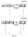
- FIG. 15is drawing of four cross-sections of an interconnect structure involving thin signal conductors.
- FIG. 16is a drawing of four cross-sections of the power connection structure of FIG. 13 attached to the interconnect structure of FIG. 15 in accordance with one novel aspect.
- FIG. 17is a cross-sectional drawing wherein die bonding bumps are disposed along the surface of the interconnect structure.
- the interconnect structureis attached to the power connection structure in accordance with one novel aspect.
- FIG. 18is a cross-sectional drawing of a semiconductor substrate showing a partial FPGA die and a plurality of power bus bar structures.
- FIG. 19is a flowchart of a novel method of making a semiconductor substrate.
- FIG. 4is drawing of a fusion bonded semiconductor substrate 250 in accordance with one novel aspect.
- a plurality of FPGA dice 270 - 273is disposed upon a semiconductor substrate.
- the substratehas a first area 265 containing a first density of through-holes, a second area 260 containing a second density of through-holes, and coolant through-holes 255 .
- the first density of through-holesallows for straight through vertical connections through the substrate at the edges of the semiconductor substrate.
- Multiple layers of semiconductor substratescan be configured in a stack with Shin-Etsu conductive filament elastomeric connectors between the substrates.
- a bus of parallel extending bus conductorsextends through the through holes and conductive filaments of the elastomeric connectors, from the top of the stack to the bottom of the stack.
- the first density of through-holesallows for four holes per each bus conductor. These through-holes extend through the wafer, are approximately 25 microns or greater in diameter, and allow for signals to pass from the semiconductor substrate of FIG. 4 to a semiconductor substrate immediately below or immediately above it when configured within a stack of multiple semiconductor substrates. This first density of through-holes within the first area of the semiconductor substrate 250 also permits FPGA die connections to be directed into and out of the semiconductor substrate.
- the second area 260 of the semiconductor substrate of FIG. 4contains a second density of through-holes that is used to couple thick conductors on the bottom plane of the semiconductor substrate to thick conductors present on multiple layers below the plurality of FPGA dice 270 - 273 .
- the through-holes in the second area 260 of the semiconductor substrate 250are of a density similar to the density of power bumps present on the bottom surfaces of the FPGA dice.
- These through-holes of the second area 260are utilized for power and ground connections which extend vertically through the semiconductor substrate 250 into laterally conducting thick conductors.
- the laterally conducting thick conductorsare then coupled through power bumps to the FPGA such to create an electrical connection characterized by less than twenty millivolts or thirty millivolts of resistive drop.
- liquid coolantis circulated below each semiconductor substrate.
- coolant through-holes 255extending completely through the semiconductor substrate permits coolant to pass through the semiconductor substrate to the upper surface of the semiconductor substrate.
- semiconductor through-holesare not disposed through the semiconductor substrate because the flow of coolant immediately below the semiconductor substrate is sufficient to prevent overheating.
- FIG. 5is a cross-sectional drawing of the semiconductor substrate of FIG. 4 .
- An interconnect structure 280 containing a “thin conductor layers portion” 540 characterized as having a plurality of thin fine-pitch conductorsis disposed onto a “power connection structure” 285 .
- a plurality of thick and wide horizontal conductorsis disposed within a “thick conductor layers portion” 298 within the power connection structure and a plurality of through-holes 24 - 26 extends vertically through a semiconductor power through-hole portion 295 within the power connection structure 285 .
- These thick and wide horizontal conductors present within the power connection structure 285are of a thickness of approximately two microns or greater.
- a conductive viais disposed within each through-hole, 24 - 26 .
- a plurality of die bonding bumps 2 - 5is disposed upon the thin conductor layers portion 540 .
- the die bumps 2 - 5are arrayed to match the corresponding array of lands 11 - 14 present on the FPGAs to be disposed onto the semiconductor substrate.
- the die bonding bumps 2 - 5conduct power to the FPGA dice through vertical vias within through-holes 24 - 26 to thick horizontal conductive layers present within the thick conductor layers portion 298 .
- the thick conductor layersare then electrically coupled to a thick conductor layer present on the bottom plane of the semiconductor power through-hole portion by the conductive vias disposed within the semiconductor power through-hole portion.
- interconnect structure 280 containing the thin conductor layers portion 540is fusion bonded to the power connection structure 285 containing the thick conductor layers portion 298 . Fusion bonding permits the planar surfaces of the interconnect structure 280 and the power connection structure 285 to contact each other physically within atomic dimensions such that direct bonds exist between the two structures obviating any need for adhesive material between the two structures.
- interconnect structure 280 and power connection structure 285are connected through the use of adhesive materials between the structures.
- FIG. 6is a drawing which shows a semiconductor substrate 602 and a semiconductor substrate 604 disposed on a semiconductor wafer 600 .
- semiconductor wafer 600is a wafer of single-crystal silicon material.
- Each semiconductor substrate shown in FIG. 6is at least two inches in width and at least one inch in length and is large enough to accommodate several FPGA dice.
- FIG. 7is a top down drawing of a semiconductor substrate portion showing a plurality of through-holes 10 , 11 , and 23 - 26 and a plurality of die bonding bumps 1 - 8 .
- Planes A and Bextend horizontally and are perpendicular to plane C and plane D.
- Plane Aintersects several through-holes 8 and die bonding bumps 9 .
- Plane C and plane Dintersect die bonding bumps 9 and no through-holes.
- Plane Bintersects the semiconductor substrate portion without intersecting through-holes 8 or die bonding bumps 9 .
- Plane Aintersects plane D at a point “W” and plane A intersects plane C at a point “X.”
- Plane Bintersects plane D at a point “Y” and plane B intersects plane C at a point “Z.”
- FIG. 8is a cross-sectional diagram of semiconductor body 300 through each of four planes A, B, C, and D.
- Semiconductor body 300is utilized in the present invention to create the semiconductor power through-hole portion.
- FIG. 9is a cross-sectional diagram of semiconductor body 300 with a plurality of through-holes 310 disposed within semiconductor body 300 .
- Through-holes 24 - 26extend through semiconductor body 300 in plane A, however, planes B, C, and D do not intersect any through-holes.
- Through-holes 24 - 26are shown extending completely through semiconductor body 300 .
- the through-holes 24 - 26are created by reactive ion etching the semiconductor body until the through-holes 24 - 26 extend from the upper surface of semiconductor body 300 through the semiconductor body to the bottom surface of semiconductor body 300 .
- FIG. 10is a cross-sectional drawing of semiconductor body 300 , a conductive layer 306 , a conductive layer 307 , and through-holes 24 - 26 .
- Conductive layer 306is disposed on top of semiconductor body 300 and conductive layer 307 is disposed on the bottom of the semiconductor body 300 .
- conductive layer 306 and conductive layer 307have partially filled through-holes 24 - 26 to create a plurality of conductive vias.
- the conductive viasextend from the conductive layer 306 on the top plane of semiconductor body 300 to conductive layer 307 disposed upon the bottom plane of semiconductor body 300 .
- Conductive layers 306 and 307may be copper, a copper-based alloy, or any similarly suitable material.
- Conductive layers 306 and 307 disposed onto semiconductor body 300have been patterned and etched in FIG. 10 .
- Conductive layers 306 and 307are patterned using dry film photoresist. Dry film photoresist is used because of the presence of the plurality of through-holes 24 - 26 at the surface of semiconductor body 300 . If wet or liquid photoresist is used, through-holes 24 - 26 do not allow for a uniform surface when the liquid resist is “spun on.” Through-holes 24 - 26 create turbulence during the spin-on process used in wet or liquid resist processing which prohibits a uniform thickness of photoresist.
- Dry film resistinvolves thicker layers of photoresistive material, and thus features smaller than twenty or thirty microns cannot be resolved using dry film photoresist because of its thickness. Therefore, while the dry film photoresist produces a pattern of conductors sufficient to route power conductors, a different approach is generally required for the thin fine pitch conductors used for high density signal routing.
- FIG. 11is a cross-sectional drawing showing an insulating layer 317 applied above the conductive layer 306 of semiconductor body 300 .
- Insulating layer 317has been patterned and etched to allow for electrical connections of subsequent applications of conductive layers. Additional conductive layers may then electrically connect to conductive layer 306 disposed on top of semiconductor body 300 .
- FIG. 12is a cross-sectional drawing showing each of four planes A, B, C, and D intersecting through power connection structure 85 of FIG. 5 .
- the power connection structureincludes a second conductive layer 318 , insulating layer 317 , conductive layer 306 , semiconductor body 300 , and conductive layer 307 .
- Second conductive layer 318is disposed above first conductive layer 306 .
- Conductive layer 318is patterned to permit contact to conductive layer 306 and conductive layer 307 at desired locations. Additionally, conductive layer 318 is patterned to allow for future locations where vias can be etched through to provide electrical connections to underlying layers.
- Conductive layer 307 disposed upon the bottom plane of semiconductor body 300has also been made thicker as another layer of conductive material has been disposed upon the bottom side of the power connection structure. Because an insulating layer is not present on the bottom of the structure of FIG. 12 , the effect is to make a thicker, less resistive conductive layer 307 disposed upon the bottom plane of semiconductor body 300 .
- Second conductive layer 318is also disposed within through-holes 24 - 26 and makes electrical connections to conductive layer 307 in desired locations. Similar to conductive layers 306 and 307 , conductive layer 318 is patterned using dry film photoresist. Dry film photoresist is used because of the presence of the plurality of through-holes 24 - 26 at the surface of semiconductor body 300 .
- FIG. 13is a cross-sectional drawing of four planes A, B, C, and D, intersecting power connection structure 285 of a semiconductor substrate as those planes are drawn in FIG. 7 .
- Power connection structure 285includes an insulating layer 309 , a plurality of interconnect vias 321 , conductive layers 306 , 307 , and 318 , insulating layer 317 , semiconductor body 300 , a power connection structure planar surface 500 , and through-holes 24 - 26 .
- Insulating layer 309is disposed above second conductive layer 318 and interconnect vias 321 have been etched to allow electrical connections to extend from the top plane of the power connection structure to conductive layer 306 and second conductive layer 318 .
- the power connection structure planar surface 500is made by polishing and cleaning the surface of power connection structure 285 within a few atoms of flatness.
- FIG. 14is a drawing of four cross-sections of a semiconductor material 530 and a thin conductive layers portion 540 .
- Thin conductive layers portion 540includes a plurality of lands 11 - 16 , interconnect vias 18 - 22 , and thin conductor layers 520 .
- This thin conductive layers portion 540may be produced by standard dual damascene processing utilizing liquid resist processing. Liquid resist processing is possible in this step of creating the structure of FIG. 14 because through-holes are not present in semiconductor material 530 nor in thin conductive layers portion 540 .
- the thin conductive layers 520are fine pitch conductors and can be made of sufficient density to pattern thousands of conductive traces necessary for interconnecting the plurality of FPGA, dice mounted at the surface of the semiconductor substrate 250 of FIG. 4 .
- the conductive layers within thin conductive layers portion 540are approximately twenty microns or less in thickness.
- Conductive vias 18 - 22have been patterned into the thin conductive layers portion 540 to allow connection to corresponding vias on the power connection structure planar surface 500 of FIG. 13 .
- FIG. 15is a drawing of four cross-sections of thin conductor layers portion 540 after semiconductor material 530 has been backlapped away.
- the removal of semiconductor material 530leaves interconnect planar surface 505 devoid of crystalline semiconductor material.
- This conductor layers portion 540includes an interconnect planar surface 505 .
- Interconnect planar surface 505is made by polishing and cleaning the surface of power connection structure 285 within a few atoms of flatness. In other embodiments, semiconductor material 530 is not backlapped until after the interconnect structure and the power connection structure are connected together.
- FIG. 16is a cross-sectional diagram showing four cross sections of a semiconductor substrate.
- the semiconductor substrateincludes thin layers portion 540 of interconnect structure 280 of FIG. 5 , and power connection structure 285 of FIG. 13 .
- the interconnect planar surface 505 of thin conductor layers portion 540 of FIG. 15is fusion bonded to power connection structure planar surface 500 of FIG. 13 .
- the surfaces of the both wafersare polished within a few atoms of flatness. This level of flatness is required for fusion bonding and the requisite level of flatness may be ensured by utilization of a sensitive photon detector.
- the wafersare then aligned using through-holes or other structures within the semiconductor substrate as a guide.
- the structuresare then brought into physical contact where atomic bonding or crystalline bonding occurs naturally. These bonds are approximately 10.5 kcal/mol and sufficient to hold the wafers firmly together.
- the single-crystalline material of the semiconductor wafer 530is backlapped from (removed from) the fusion bonded structure and die bonding bumps 1 - 8 are added.
- FIG. 17is a drawing showing four cross-sections of a semiconductor substrate 250 of FIG. 4 .
- the cross-sections shownare planes A, B, C, and D of FIG. 7 .
- Semiconductor substrate 250includes die bonding bumps 2 - 7 , lands 11 - 16 , interconnect vias 18 - 22 , interconnect structure 280 and power connection structure 285 .
- a network 28 of conductive metalis disposed within the power connection structure 285 .
- a second network 29 of conductive metalis also disposed within power connection structure 285 ; second network 29 is electrically isolated from network 28 . Electrical connections are present from the top of the semiconductor substrate 250 to a conductive layer on the bottom of semiconductor substrate 250 .
- FIG. 17is a drawing showing four cross-sections of a semiconductor substrate 250 of FIG. 4 . The cross-sections shown are planes A, B, C, and D of FIG. 7 .
- Semiconductor substrate 250includes die bonding bumps 2 - 7 ,
- die bonding bump 5in plane A, is electrically connected to land 14 .
- Land 14is further electrically connected to interconnect via 20 which is electrically connected to network 29 within the power connection structure 285 .
- Network 29is electrically connected via conductive metal within through-hole 26 to a portion of conductive layer 307 of FIG. 13 .
- Conductive network 28is electrically isolated from conductive network 29 and electrically connects die bonding bump 4 to a portion of an electrically conductive layer on the bottom of semiconductor substrate 250 .
- die bonding bump 4is electrically connected to land 13 which is electrically connected to conductive network 28 through interconnect via 19 .
- a conductor of conductive network 28extends perpendicularly to plane A to a point “Z” in plane C where it then extends horizontally from point “Z” to point “Y” in plane B.
- the conductorthen extends perpendicularly in plane D to a point “W” where it extends into plane A and makes electrical contact via through-hole 24 to a portion of conductive layer 307 of FIG. 13 .
- FIG. 18is a cross-sectional drawing of a semiconductor substrate 250 showing a partial FPGA die 270 and a plurality of power bus bar structures. Decoupling capacitors 812 and 814 are shown disposed between the power bus bar structures 820 - 823 .
- the power bus bar structuresare solid copper bars approximately 1.5 millimeters high by 1.5 millimeters wide. There are about ten copper power bus bars under each FPGA die and each power bus bar spans the entire width of the semiconductor substrate. Each copper bus bar may provide for a hundred or more vertical connections facilitated by the vertical through-holes such that the voltage drop from bus bar to FPGA is less than approximately twenty to thirty millivolts.
- the vertical through-holesalso strengthen the structure by riveting the copper plane located on the bottom plane of the semiconductor substrate to the semiconductor substrate.
- FIG. 19is a flowchart of a novel method of making a semiconductor substrate.
- a first semiconductor waferis processed to create a plurality of through-holes. Through-holes, approximately sixty microns in diameter, are etched through the wafer. Each through-hole extends through the semiconductor wafer. The through-holes (in second area 260 of FIG. 4 ) are spaced four-hundred microns apart.
- the first semiconductor waferis processed to create a power connection structure.
- the power connection structureincludes a relatively thick horizontally extending conductor.
- dry film processingis used. Dry film processing is not incompatible with the through-holes present in the wafer.
- a second semiconductor waferis processed to create a relatively thin horizontally extending conductor.
- the thin horizontally extending conductorsare of fine pitch and are created by dual damascene processing or other well known methods. Connections are also present in the interconnect structure that will align with and electrically couple to the thick horizontally extending conductors within the power connection structure.
- the interconnect structure 280is fusion bonded to the power connection structure 285 to create a semiconductor substrate 250 .
- the surfaces of both structuresare polished within a few atoms of flatness.
- the wafersare then aligned using through-holes or other structures within the semiconductor substrate as a guide.
- the structuresare then brought into physical contact where atomic bonding or crystalline bonding occurs naturally.
- a fifth step 845the second semiconductor wafer is removed from the interconnect structure.
- the semiconductor wafer portionis removed by backlapping. After removal, the interconnect structure including the relatively thin horizontally extending conductors remains.
Landscapes
- Engineering & Computer Science (AREA)
- Microelectronics & Electronic Packaging (AREA)
- Power Engineering (AREA)
- Computer Hardware Design (AREA)
- Physics & Mathematics (AREA)
- Condensed Matter Physics & Semiconductors (AREA)
- Thermal Sciences (AREA)
- General Physics & Mathematics (AREA)
- Internal Circuitry In Semiconductor Integrated Circuit Devices (AREA)
- Coupling Device And Connection With Printed Circuit (AREA)
- Testing Of Individual Semiconductor Devices (AREA)
- Semiconductor Integrated Circuits (AREA)
- Design And Manufacture Of Integrated Circuits (AREA)
- Cooling Or The Like Of Electrical Apparatus (AREA)
- Cooling Or The Like Of Semiconductors Or Solid State Devices (AREA)
Abstract
Description
- This application is based on and hereby claims the benefit under 35 U.S.C. §119 from U.S. Provisional Application No. 60/995,194, entitled “Semiconductor Substrate Stack High Performance Computer,” filed on Sep. 24, 2007, the subject matter of which is incorporated herein by reference.
- The described embodiments relate to packaging semiconductor devices characterized by a large number of high speed signal and power connections combined with high power consumption.
- The current state of the art of semiconductor development is the mass production of large integrated circuits “IC's” containing several million active components. One type of device fitting this description is a large Field Programmable Gate Array “FPGA.” FPGAs and other devices may operate at speeds of several hundred Megahertz and it is not unusual that these integrated circuits include over a thousand pins that bring high speed signals into and out of the integrated circuit die. With a large number of active internal components switching at high speeds, these devices consume large amounts of power. Therefore it is necessary to have a packaging solution that allows for the distribution of over a thousand high speed signal lines and also provides for a plurality of connections to supply power to the device. To solve this problem for a single FPGA, IC designers have used a technique wherein thousands of “bumps” are distributed over the surface of the FPGA via thick metal lines. It would not be unusual to have two-thousand bumps for power and another two thousand for ground. The large number of bumps reserved for power ensures only a minimal resistive drop from the surface of the device to the active devices within the FPGA.
- The power and signal connections extend from the bumps present on the surface of the FPGA to balls of a ball-grid-array “BGA” package. A BGA utilized for packaging a large FPGA has approximately fifteen-hundred balls; one-thousand for input and output “I/O” connections and five-hundred for power and ground connections. Power is supplied to the balls of the BGA package through thick metal conductors to the bumps present on the surface of the FPGA.
- The bumped FPGA construction and BGA package is adequate to power and connect a single FPGA but it is not adequate to power and connect a system of many FPGAs. The problems associated with the large number of signals and the high power requirements of a single FPGA are multiplied when several devices are required for use within a single system. In this case, many thick conductors are needed for power connections while many minimum width conductors are required for routing high speed input and output signals. Thus a larger substrate is needed for the increased routing requirements while, the area needed for routing all of these signals should be minimized for the highest possible system performance.
- Improved performance is obtained with the utilization of a silicon wafer as a semiconductor substrate. Even with the use of a silicon substrate, however, multiple layers with multiple cross-overs are used to route the large number of signals and power. The addition of multiple layers to allow for the requisite signal density further decreases performance and increases fabrication costs.
- U.S. Pat. No. 6,221,769 discusses a method to decrease the density of signal lines and increase performance by creating a semiconductor chip package having a silicon substrate with substrate vias for connecting to a power source and other electronic devices. As shown in
FIG. 1 (Prior Art), a plurality ofintegrated circuit dice 100 are connected tomultilevel wiring layer 107 using diebonding bumps 109. Power is routed from integrated circuit die100 through diebonding bumps 109 through themultilevel wiring layer 107 and to thebonding balls 103 via throughsubstrate vias 105. - U.S. Pat. No. 5,236,118 describes a process for aligning and bonding of complimentary electrical structures and is hereby incorporated by reference. The described process is applicable to fabrication of semiconductor devices from separate structures and employs direct silicon bonding.
FIG. 2 (Prior Art) shows a similar structure except power is routed from the integrated circuit die100 tocontacts 110 using through-substrate vias 105.Contacts 110 can be a grid array made of ceramic or a copper based material. The prior art describes a method for drilling three thousand to five thousand substrate vias through the wafer, the substrate vias having a one millimeter diameter with one millimeter spacing. Once the substrate vias have been created in the prior art process, the vias are electroplated and standard dual damascene processing forms the multilevel wiring that connects to the substrate vias.- If standard spin-on resist processing, used to create the multilevel wiring structures, is performed with unfilled through substrate vias present in the wafer, uneven thicknesses of photoresist during spin-on of the photoresist material will occur over the surface of the wafer. Etching of the photoresist will not be uniform resulting in a large number of defects and increased fabrication cost or reduced wafer yield. This method is not suitable for mass manufacturing.
- Dry film resist processing for the multilevel wiring will not have the uneven thickness issues present with wet or liquid resist processing and can be used to create thick conductors used for power routing. However, dry film processing is not suitable for feature sizes of less than twenty or thirty microns and thus dry film processing is not suitable for creation of conductors required for routing thousands of signal lines.
- U.S. Pat. No. 6,379,982 discusses a semiconductor wafer-on-wafer package which is shown in
FIG. 3 (Prior Art).FIG. 3 displays a cross-sectional drawing of a portion of an unsingulated die of a wafer-on-wafer package, the wafer-on-wafer package constructed for the purpose of testing and burning-in the die prior to singulation. InFIG. 3 ,die bond pad 202 is shown protruding slightly from the surface ofdevice wafer 200 which is the active surface of a semiconductor die contained therein.Conductive trace 215, which may be copper, a copper based alloy, or any suitable electrically conductive material is disposed onsupport wafer 225 and is shown contacting bondpad connection point 204. The bond pad connection point is a solder ball or bump and is disposed uponconductive trace 215. Through-wafer via210 is preformed insupport wafer 225 prior to attachingdevice wafer 200 to supportwafer 225. The through-wafer via is created by laser drilling, electrochemical anodization, or by an etching process and has an internal diameter of approximately sixty microns.Conductive filling material 206 is disposed within through-wafer via210 such that an electrical connection is made to device wafer200 via diebond 202, by bondpad connection point 204,conductive filling material 206 andbump 207.Bump 207 is electrically conductive and is used to make electrical contact to mountingpad 208 ofmounting substrate 206.Gap 201 is shown between thedevice wafer 200 andpassivation layer 205. While the prior art drawing inFIG. 3 illustrates a method of producing a silicon package with through-wafer vias, the silicon packages described do not provide connections to multiple semiconductor integrated circuits disposed ondevice wafer 200. Thus the wafer-on-wafer package does not appear to have multiple conductive layers of varying thicknesses necessary both to provide power and to route thousands of connections from one semiconductor IC to another. - A method of making a semiconductor package is therefore desired which supports; 1) construction of thin, fine-pitch conductors for routing signal connections between a plurality of semiconductor ICs, 2) construction of thick conductors, characterized as having large feature sizes, for the lateral conduction of power to the semiconductor ICs and 3) through-holes for conducting the power supply through a semiconductor body to facilitate the increased density of thin conductors between semiconductor ICs on the silicon substrate.
- A plurality of FPGA dice or other components are disposed upon a semiconductor substrate. In order to 1) connect thousands of interconnect lines between the FPGA die and 2) supply the immense amount of power required for these types of devices, it is necessary to construct a package out of a semiconductor substrate. It is also necessary that the construction of the package includes two different portions that are built using incompatible processes. The first of such portions is an interconnect structure containing a thin conductor layers portion characterized as having a plurality of thin fine-pitch conductors. These fine-pitch conductors are used to make high speed and other signal connections between the multiple FPGA dice. Produced by standard dual damascene processing utilizing wet resist processing, the thin conductive layers are approximately less than one micron thick and less than twenty microns in width. Using this type of processing, the thin fine-pitch conductive layers can be made of sufficient density to pattern thousands of conductive traces necessary for interconnecting the plurality of FPGA dice mounted at the surface of the semiconductor substrate.
- For the power connections, these interconnect types of connections are not thick enough to bring in power supply currents into the FPGA devices and even if these layers could be used, the additional area required to route the power connections would reduce area needed for the high density interconnect conductors. In addition, the conductor materials for power routing may be different than conductor material used for interconnect signal layers. Therefore a second structure is required to sufficiently route power to the plurality of FPGA dice. This second structure, a power connection structure, includes thick conductors and vertical through-holes. It is due to these vertical through-holes that the processing used to create the power connection structure may be different from, and incompatible with, the process used to create the interconnect structure. The thick conductive layers are patterned using dry film resist. Dry film resist is used because of the presence of the through-holes on the surface of the power connection structure. If wet resist is used, the conductive through-holes do not allow for a uniform surface during spin-on of wet photoresist. Additionally, dry resist is a lower cost process than wet or liquid resist processing. Turbulence caused by the through-holes during the spin-on processing of liquid photoresist prohibits a uniform thickness of that material. Because dry film resist processing involves thicker layers of photoresistive material that spans the open via holes, minimum feature size issues are associated with dry film processing. Feature sizes, line widths and spacing, smaller than twenty or thirty microns cannot be resolved using dry film photoresist because of its thickness. Therefore while the dry film resist produces a pattern of conductors sufficient to route power conductors, it is impossible to obtain the density required for creating conductors useful for high density signal routing.
- As stated above, the power connection structure contains conductive through-holes and thick conductor layers. The through-holes, approximately 25 microns or greater in diameter, are used to electrically couple thick conductors on the bottom plane of the semiconductor substrate to thick conductors present on multiple layers below the plurality of FPGA dice. The through-holes in this power connection structure are partially or completely filled by a conductive material and are of a density similar to the density of power bumps present on FPGA dice mounted to the semiconductor substrate. These through-holes are utilized for power and ground connections which extend vertically through the semiconductor substrate into laterally extending thick conductors. The thickness of the substrate may be approximately seven hundred microns.
- The lateral thick conductors are approximately two microns or more in thickness and are used to traverse a minimum lateral distance before they can be routed to the surface of the semiconductor substrate and into an FPGA die via bonding bumps disposed upon the surface of the semiconductor substrate. These die bonding bumps are arrayed to match the corresponding array of lands present on the particular FPGA's to be attached to the semiconductor substrate. Coupled to the underside of the semiconductor substrate below the thick conductor layers is a plurality of power bus bar structures with decoupling capacitors disposed between the power bus bar structures. These power bus bar structures are made of copper or a similar conductive material and are approximately 1.5 millimeters high by 1.5 millimeters wide. There are ten or so of these power bus bars under each FPGA die and each power bus bar spans the entire width of the semiconductor substrate. Each copper bus bar may have a hundred or more vertical connections facilitated by the vertical through-hole conductors such that the IR drop is less than approximately twenty to thirty millivolts. This small amount of loss can be compensated for by a similar increase in the power supply used to supply the FPGA devices. During processing, expansion and contraction caused by rapid heating to a high temperature and subsequent cooling stresses the power connection structure at the junction of different materials. The vertical through-holes also serve to reduce stress at the junction of the copper plane and semiconductor material by riveting the copper plane to the semiconductor substrate at thousands of locations.
- Both the interconnect structure and the power connection structure are greater than two inches on one side and are each constructed on a wafer that only contains like structures. This is necessitated by the incompatible processing requirements of each type of structure. To connect the two structures together, they are joined at the wafer level and then singulated. In other embodiments, the singulation from the wafers occurs before the power connection structure and interconnect structure are bonded together. This process allows for both structures to be tested independent of the other and defective structures can be removed from the process before adhesion to the other type of structure. In yet another embodiment, the power connection structure is manufactured and then singulated tested good interconnect structures are added to the power connection structures. This permits better overall yield and manufacturability of the semiconductor substrate. To join the two wafers, the surface of the each wafer is polished to within a few atoms of flatness and subsequently cleaned. The wafers are then aligned utilizing through-holes or other structures as guides. The wafers are then brought into physical contact where atomic or crystalline bonding occurs naturally and without the use of adhesives. This process, fusion bonding, produces bonds of approximately 10.5 kcal/mol which are sufficient to hold the wafers firmly together. After the two wafers are fusion bonded, additional processing may be performed, for example, vias may be disposed onto the fusion bonded structure. Additionally, die bond pads and bumps are added to the surface of the interconnect structure to facilitate mounting of the multiple FPGA dice.
- Once completed, multiple layers of semiconductor substrates can be included within a single system by creating a stack of semiconductor substrates joined with Shin-Etsu conductive filament elastomeric connectors disposed between the substrates. Through-holes are positioned within a first area which includes a first density of four holes per each bus conductor. These through-holes, approximately 25 microns or greater in diameter, allow for signals to pass from one semiconductor substrate to semiconductor substrates above or below it when configured within a stack of multiple semiconductor substrates. This first density of through-holes within the first area of the semiconductor substrate also permits the connections of the plurality of FPGA dice to be directed into and out of each semiconductor substrate.
- In other embodiments, processes that are incompatible due to temperatures used in processing may be combined by fusion bonding. In yet another embodiment, structures created by high cost or low-yielding processes may be combined with structures manufactured via low cost, high-yield processes by fusion bonding the incompatible structures.
- Further details, embodiments and techniques are described in the detailed description below. This summary does not purport to define the invention. The invention is defined by the claims.
- The accompanying drawings, where like numerals indicate like components, illustrate embodiments of the invention.
FIG. 1 (Prior Art) is a cross-sectional diagram of a plurality of integrated circuit dice mounted on a semiconductor substrate containing a plurality of through substrate vias.FIG. 2 (Prior Art) is a cross-sectional diagram of a semiconductor substrate showing a plurality of contacts disposed along the bottom surface of the semiconductor substrate.FIG. 3 (Prior Art) is a cross-sectional view of an unsingulated die mounted upon a semiconductor substrate with a single through-wafer via extending through a semiconductor support wafer.FIG. 4 is a perspective view of a plurality of FPGA dice mounted upon a semiconductor substrate.FIG. 5 is a cross-sectional diagram of the semiconductor substrate ofFIG. 4 with an interconnect structure adhered to a power connection structure showing a plurality of through-holes in accordance with one novel aspect.FIG. 6 is a diagram of how two semiconductor substrates are cut from a semiconductor wafer.FIG. 7 is a top down diagram of a semiconductor substrate portion with four planes extending through the semiconductor substrate.FIG. 8 is a cross-sectional drawing through each of four planes of a semiconductor body utilized in the invention.FIG. 9 is drawing of four cross-sections of a semiconductor body, one of the planes having a plurality of through-holes.FIG. 10 is drawing of four cross-sections of the semiconductor body having a plurality of through-holes. A conductive layer has been disposed within the through-holes and on the top and bottom surfaces of the semiconductor body.FIG. 11 is a drawing of four cross-sections of a semiconductor body. A layer of insulating material has been disposed upon one side of the semiconductor body and etched to allow for subsequent connections to be made to the conductive layer disposed below the insulating material.FIG. 12 is a drawing showing four cross-sections wherein a second conductive layer is disposed upon the layer of insulating material. A second conductive layer has been deposited on the bottom surface and etched in a desired manner.FIG. 13 is a drawing of a power connection structure in accordance with the present invention. Four cross-sections are shown.FIG. 14 is drawing of four cross-sections wherein a plurality of thin conductive layers is disposed upon one side of a substrate of semiconductor material.FIG. 15 is drawing of four cross-sections of an interconnect structure involving thin signal conductors.FIG. 16 is a drawing of four cross-sections of the power connection structure ofFIG. 13 attached to the interconnect structure ofFIG. 15 in accordance with one novel aspect.FIG. 17 is a cross-sectional drawing wherein die bonding bumps are disposed along the surface of the interconnect structure. The interconnect structure is attached to the power connection structure in accordance with one novel aspect.FIG. 18 is a cross-sectional drawing of a semiconductor substrate showing a partial FPGA die and a plurality of power bus bar structures.FIG. 19 is a flowchart of a novel method of making a semiconductor substrate.FIG. 4 is drawing of a fusion bondedsemiconductor substrate 250 in accordance with one novel aspect. A plurality of FPGA dice270-273 is disposed upon a semiconductor substrate. The substrate has afirst area 265 containing a first density of through-holes, asecond area 260 containing a second density of through-holes, and coolant through-holes 255. The first density of through-holes allows for straight through vertical connections through the substrate at the edges of the semiconductor substrate. Multiple layers of semiconductor substrates can be configured in a stack with Shin-Etsu conductive filament elastomeric connectors between the substrates. A bus of parallel extending bus conductors extends through the through holes and conductive filaments of the elastomeric connectors, from the top of the stack to the bottom of the stack. The first density of through-holes allows for four holes per each bus conductor. These through-holes extend through the wafer, are approximately 25 microns or greater in diameter, and allow for signals to pass from the semiconductor substrate ofFIG. 4 to a semiconductor substrate immediately below or immediately above it when configured within a stack of multiple semiconductor substrates. This first density of through-holes within the first area of thesemiconductor substrate 250 also permits FPGA die connections to be directed into and out of the semiconductor substrate.- The
second area 260 of the semiconductor substrate ofFIG. 4 contains a second density of through-holes that is used to couple thick conductors on the bottom plane of the semiconductor substrate to thick conductors present on multiple layers below the plurality of FPGA dice270-273. The through-holes in thesecond area 260 of thesemiconductor substrate 250 are of a density similar to the density of power bumps present on the bottom surfaces of the FPGA dice. These through-holes of thesecond area 260 are utilized for power and ground connections which extend vertically through thesemiconductor substrate 250 into laterally conducting thick conductors. The laterally conducting thick conductors are then coupled through power bumps to the FPGA such to create an electrical connection characterized by less than twenty millivolts or thirty millivolts of resistive drop. In a system containing multiple layers of semiconductor substrates it is foreseeable that power in the range of several kilowatts may be consumed. To prevent overheating, liquid coolant is circulated below each semiconductor substrate. The presence of coolant through-holes 255 extending completely through the semiconductor substrate permits coolant to pass through the semiconductor substrate to the upper surface of the semiconductor substrate. In another embodiment, semiconductor through-holes are not disposed through the semiconductor substrate because the flow of coolant immediately below the semiconductor substrate is sufficient to prevent overheating. FIG. 5 is a cross-sectional drawing of the semiconductor substrate ofFIG. 4 . Aninterconnect structure 280 containing a “thin conductor layers portion”540 characterized as having a plurality of thin fine-pitch conductors is disposed onto a “power connection structure”285. A plurality of thick and wide horizontal conductors is disposed within a “thick conductor layers portion”298 within the power connection structure and a plurality of through-holes24-26 extends vertically through a semiconductor power through-hole portion 295 within thepower connection structure 285. These thick and wide horizontal conductors present within thepower connection structure 285 are of a thickness of approximately two microns or greater. A conductive via is disposed within each through-hole,24-26. A plurality of die bonding bumps2-5 is disposed upon the thin conductor layersportion 540. The die bumps2-5 are arrayed to match the corresponding array of lands11-14 present on the FPGAs to be disposed onto the semiconductor substrate. The die bonding bumps2-5 conduct power to the FPGA dice through vertical vias within through-holes24-26 to thick horizontal conductive layers present within the thick conductor layersportion 298. The thick conductor layers are then electrically coupled to a thick conductor layer present on the bottom plane of the semiconductor power through-hole portion by the conductive vias disposed within the semiconductor power through-hole portion. In this manner, a large amount of current required by the FPGA devices is conducted vertically through thepower connection structure 285 to thick conductors within the thick conductor layersportion 298 to vias18-20 extending through theinterconnect structure 280 to lands11-14 and then to die bonding bumps2-5 that interface to the power connections disposed upon the surface of the FPGA. This provides for low resistance power connections through the substrate while simultaneously allowing the maximum density of thin fine-pitch conductor interconnects within theinterconnect structure 280 for routing signals between the plurality of FPGA dice disposed on the semiconductor substrate.- In this
FIG. 5 ,interconnect structure 280 containing the thin conductor layersportion 540 is fusion bonded to thepower connection structure 285 containing the thick conductor layersportion 298. Fusion bonding permits the planar surfaces of theinterconnect structure 280 and thepower connection structure 285 to contact each other physically within atomic dimensions such that direct bonds exist between the two structures obviating any need for adhesive material between the two structures. In another embodiment,interconnect structure 280 andpower connection structure 285 are connected through the use of adhesive materials between the structures. FIG. 6 is a drawing which shows asemiconductor substrate 602 and asemiconductor substrate 604 disposed on asemiconductor wafer 600. In this example,semiconductor wafer 600 is a wafer of single-crystal silicon material. Each semiconductor substrate shown inFIG. 6 is at least two inches in width and at least one inch in length and is large enough to accommodate several FPGA dice.FIG. 7 is a top down drawing of a semiconductor substrate portion showing a plurality of through-holes holes 8 and die bonding bumps9. Plane C and plane D intersect die bonding bumps9 and no through-holes. Plane B intersects the semiconductor substrate portion without intersecting through-holes 8 or die bonding bumps9. Plane A intersects plane D at a point “W” and plane A intersects plane C at a point “X.” Plane B intersects plane D at a point “Y” and plane B intersects plane C at a point “Z.”FIG. 8 is a cross-sectional diagram ofsemiconductor body 300 through each of four planes A, B, C, andD. Semiconductor body 300 is utilized in the present invention to create the semiconductor power through-hole portion.FIG. 9 is a cross-sectional diagram ofsemiconductor body 300 with a plurality of through-holes310 disposed withinsemiconductor body 300. Through-holes24-26 extend throughsemiconductor body 300 in plane A, however, planes B, C, and D do not intersect any through-holes. Through-holes24-26 are shown extending completely throughsemiconductor body 300. The through-holes24-26 are created by reactive ion etching the semiconductor body until the through-holes24-26 extend from the upper surface ofsemiconductor body 300 through the semiconductor body to the bottom surface ofsemiconductor body 300.FIG. 10 is a cross-sectional drawing ofsemiconductor body 300, aconductive layer 306, aconductive layer 307, and through-holes24-26.Conductive layer 306 is disposed on top ofsemiconductor body 300 andconductive layer 307 is disposed on the bottom of thesemiconductor body 300. As shown inFIG. 10 ,conductive layer 306 andconductive layer 307 have partially filled through-holes24-26 to create a plurality of conductive vias. The conductive vias extend from theconductive layer 306 on the top plane ofsemiconductor body 300 toconductive layer 307 disposed upon the bottom plane ofsemiconductor body 300.Conductive layers Conductive layers semiconductor body 300 have been patterned and etched inFIG. 10 .Conductive layers semiconductor body 300. If wet or liquid photoresist is used, through-holes24-26 do not allow for a uniform surface when the liquid resist is “spun on.” Through-holes24-26 create turbulence during the spin-on process used in wet or liquid resist processing which prohibits a uniform thickness of photoresist. Dry film resist involves thicker layers of photoresistive material, and thus features smaller than twenty or thirty microns cannot be resolved using dry film photoresist because of its thickness. Therefore, while the dry film photoresist produces a pattern of conductors sufficient to route power conductors, a different approach is generally required for the thin fine pitch conductors used for high density signal routing.FIG. 11 is a cross-sectional drawing showing an insulatinglayer 317 applied above theconductive layer 306 ofsemiconductor body 300. Insulatinglayer 317 has been patterned and etched to allow for electrical connections of subsequent applications of conductive layers. Additional conductive layers may then electrically connect toconductive layer 306 disposed on top ofsemiconductor body 300.FIG. 12 is a cross-sectional drawing showing each of four planes A, B, C, and D intersecting through power connection structure85 ofFIG. 5 . The power connection structure includes a secondconductive layer 318, insulatinglayer 317,conductive layer 306,semiconductor body 300, andconductive layer 307. Secondconductive layer 318 is disposed above firstconductive layer 306.Conductive layer 318 is patterned to permit contact toconductive layer 306 andconductive layer 307 at desired locations. Additionally,conductive layer 318 is patterned to allow for future locations where vias can be etched through to provide electrical connections to underlying layers.Conductive layer 307 disposed upon the bottom plane ofsemiconductor body 300 has also been made thicker as another layer of conductive material has been disposed upon the bottom side of the power connection structure. Because an insulating layer is not present on the bottom of the structure ofFIG. 12 , the effect is to make a thicker, less resistiveconductive layer 307 disposed upon the bottom plane ofsemiconductor body 300. Secondconductive layer 318 is also disposed within through-holes24-26 and makes electrical connections toconductive layer 307 in desired locations. Similar toconductive layers conductive layer 318 is patterned using dry film photoresist. Dry film photoresist is used because of the presence of the plurality of through-holes24-26 at the surface ofsemiconductor body 300.FIG. 13 is a cross-sectional drawing of four planes A, B, C, and D, intersectingpower connection structure 285 of a semiconductor substrate as those planes are drawn inFIG. 7 .Power connection structure 285 includes an insulatinglayer 309, a plurality ofinterconnect vias 321,conductive layers layer 317,semiconductor body 300, a power connection structureplanar surface 500, and through-holes24-26. Insulatinglayer 309 is disposed above secondconductive layer 318 andinterconnect vias 321 have been etched to allow electrical connections to extend from the top plane of the power connection structure toconductive layer 306 and secondconductive layer 318. The power connection structureplanar surface 500 is made by polishing and cleaning the surface ofpower connection structure 285 within a few atoms of flatness.FIG. 14 is a drawing of four cross-sections of asemiconductor material 530 and a thinconductive layers portion 540. Thinconductive layers portion 540 includes a plurality of lands11-16, interconnect vias18-22, and thin conductor layers520. This thinconductive layers portion 540 may be produced by standard dual damascene processing utilizing liquid resist processing. Liquid resist processing is possible in this step of creating the structure ofFIG. 14 because through-holes are not present insemiconductor material 530 nor in thinconductive layers portion 540. As a result of a different processing technique for the thin conductor layersportion 540, the thinconductive layers 520 are fine pitch conductors and can be made of sufficient density to pattern thousands of conductive traces necessary for interconnecting the plurality of FPGA, dice mounted at the surface of thesemiconductor substrate 250 ofFIG. 4 . The conductive layers within thinconductive layers portion 540 are approximately twenty microns or less in thickness. Conductive vias18-22 have been patterned into the thinconductive layers portion 540 to allow connection to corresponding vias on the power connection structureplanar surface 500 ofFIG. 13 .FIG. 15 is a drawing of four cross-sections of thin conductor layersportion 540 aftersemiconductor material 530 has been backlapped away. The removal ofsemiconductor material 530 leaves interconnectplanar surface 505 devoid of crystalline semiconductor material. This conductor layersportion 540 includes an interconnectplanar surface 505. Interconnectplanar surface 505 is made by polishing and cleaning the surface ofpower connection structure 285 within a few atoms of flatness. In other embodiments,semiconductor material 530 is not backlapped until after the interconnect structure and the power connection structure are connected together.FIG. 16 is a cross-sectional diagram showing four cross sections of a semiconductor substrate. The semiconductor substrate includesthin layers portion 540 ofinterconnect structure 280 ofFIG. 5 , andpower connection structure 285 ofFIG. 13 . The interconnectplanar surface 505 of thin conductor layersportion 540 ofFIG. 15 is fusion bonded to power connection structureplanar surface 500 ofFIG. 13 . To fusion bond a wafer containing power connection structures to a wafer containing interconnect structures, the surfaces of the both wafers are polished within a few atoms of flatness. This level of flatness is required for fusion bonding and the requisite level of flatness may be ensured by utilization of a sensitive photon detector. The wafers are then aligned using through-holes or other structures within the semiconductor substrate as a guide. The structures are then brought into physical contact where atomic bonding or crystalline bonding occurs naturally. These bonds are approximately 10.5 kcal/mol and sufficient to hold the wafers firmly together. After fusion bonding, the single-crystalline material of thesemiconductor wafer 530 is backlapped from (removed from) the fusion bonded structure and die bonding bumps1-8 are added. By creating the power connection and the interconnect structures separately on different wafers, an additional advantage is obtained because the wafers containing the high density, fine pitch, thin conductors of the interconnect structure can be tested independently from the power connection structures and defective wafers can be discarded before they are attached to non-defective power connection structure wafers. Additionally, die bond pads535 are shown at the surface of the interconnect structure inFIG. 16 . Lastly the individual semiconductor substrates are singulated from the fusion bonded wafers for attachment of components, power bus bars and connectors.FIG. 17 is a drawing showing four cross-sections of asemiconductor substrate 250 ofFIG. 4 . The cross-sections shown are planes A, B, C, and D ofFIG. 7 .Semiconductor substrate 250 includes die bonding bumps2-7, lands11-16, interconnect vias18-22,interconnect structure 280 andpower connection structure 285. Anetwork 28 of conductive metal is disposed within thepower connection structure 285. Asecond network 29 of conductive metal is also disposed withinpower connection structure 285;second network 29 is electrically isolated fromnetwork 28. Electrical connections are present from the top of thesemiconductor substrate 250 to a conductive layer on the bottom ofsemiconductor substrate 250. In the semiconductor substrate ofFIG. 17 , diebonding bump 5, in plane A, is electrically connected to land14.Land 14 is further electrically connected to interconnect via20 which is electrically connected to network29 within thepower connection structure 285.Network 29 is electrically connected via conductive metal within through-hole 26 to a portion ofconductive layer 307 ofFIG. 13 .Conductive network 28 is electrically isolated fromconductive network 29 and electrically connects diebonding bump 4 to a portion of an electrically conductive layer on the bottom ofsemiconductor substrate 250. Shown in plane A ofFIG. 17 , diebonding bump 4 is electrically connected to land13 which is electrically connected toconductive network 28 through interconnect via19. At point “X” in plane C, a conductor ofconductive network 28 extends perpendicularly to plane A to a point “Z” in plane C where it then extends horizontally from point “Z” to point “Y” in plane B. The conductor then extends perpendicularly in plane D to a point “W” where it extends into plane A and makes electrical contact via through-hole 24 to a portion ofconductive layer 307 ofFIG. 13 .FIG. 18 is a cross-sectional drawing of asemiconductor substrate 250 showing a partial FPGA die270 and a plurality of power bus bar structures.Decoupling capacitors FIG. 19 is a flowchart of a novel method of making a semiconductor substrate. In a first step841 a first semiconductor wafer is processed to create a plurality of through-holes. Through-holes, approximately sixty microns in diameter, are etched through the wafer. Each through-hole extends through the semiconductor wafer. The through-holes (insecond area 260 ofFIG. 4 ) are spaced four-hundred microns apart.- In a
second step 842, the first semiconductor wafer is processed to create a power connection structure. The power connection structure includes a relatively thick horizontally extending conductor. To process the horizontal conductor, dry film processing is used. Dry film processing is not incompatible with the through-holes present in the wafer. - In a
third step 843, a second semiconductor wafer is processed to create a relatively thin horizontally extending conductor. The thin horizontally extending conductors are of fine pitch and are created by dual damascene processing or other well known methods. Connections are also present in the interconnect structure that will align with and electrically couple to the thick horizontally extending conductors within the power connection structure. - In a
fourth step 844, theinterconnect structure 280 is fusion bonded to thepower connection structure 285 to create asemiconductor substrate 250. To fusion bond the two structures, the surfaces of both structures are polished within a few atoms of flatness. The wafers are then aligned using through-holes or other structures within the semiconductor substrate as a guide. The structures are then brought into physical contact where atomic bonding or crystalline bonding occurs naturally. - In a
fifth step 845, the second semiconductor wafer is removed from the interconnect structure. The semiconductor wafer portion is removed by backlapping. After removal, the interconnect structure including the relatively thin horizontally extending conductors remains. - Although certain specific embodiments are described above for instructional purposes, the teachings of this patent document have general applicability and are not limited to the specific embodiments described above. Although an example is described above where bare FPGA integrated circuit die are surface mounted to a semiconductor substrate, in other embodiments packaged FPGA integrated circuits are attached to the semiconductor substrate. Accordingly, various modifications, adaptations, and combinations of various features of the described embodiments can be practiced without departing from the scope of the invention as set forth in the claims.
Claims (22)
Priority Applications (2)
| Application Number | Priority Date | Filing Date | Title |
|---|---|---|---|
| US11/975,966US7944041B2 (en) | 2007-09-24 | 2007-10-22 | Integrated semiconductor substrate structure using incompatible processes |
| US13/065,976US8222086B2 (en) | 2007-09-24 | 2011-04-04 | Integrated semiconductor substrate structure using incompatible processes |
Applications Claiming Priority (2)
| Application Number | Priority Date | Filing Date | Title |
|---|---|---|---|
| US99519407P | 2007-09-24 | 2007-09-24 | |
| US11/975,966US7944041B2 (en) | 2007-09-24 | 2007-10-22 | Integrated semiconductor substrate structure using incompatible processes |
Related Child Applications (1)
| Application Number | Title | Priority Date | Filing Date |
|---|---|---|---|
| US13/065,976ContinuationUS8222086B2 (en) | 2007-09-24 | 2011-04-04 | Integrated semiconductor substrate structure using incompatible processes |
Publications (2)
| Publication Number | Publication Date |
|---|---|
| US20090079059A1true US20090079059A1 (en) | 2009-03-26 |
| US7944041B2 US7944041B2 (en) | 2011-05-17 |
Family
ID=40470756
Family Applications (8)
| Application Number | Title | Priority Date | Filing Date |
|---|---|---|---|
| US11/975,058Active2028-03-24US7999388B2 (en) | 2007-09-24 | 2007-10-16 | Preventing breakage of long metal signal conductors on semiconductor substrates |
| US11/975,007Active2028-05-01US7829994B2 (en) | 2007-09-24 | 2007-10-16 | Semiconductor substrate elastomeric stack |
| US11/975,011Active2028-05-08US7764498B2 (en) | 2007-09-24 | 2007-10-16 | Comb-shaped power bus bar assembly structure having integrated capacitors |
| US11/975,966Active2028-01-26US7944041B2 (en) | 2007-09-24 | 2007-10-22 | Integrated semiconductor substrate structure using incompatible processes |
| US11/981,853Active2028-10-19US7831874B2 (en) | 2007-09-24 | 2007-10-31 | Local defect memories on semiconductor substrates in a stack computer |
| US11/999,747Expired - Fee RelatedUS7719844B2 (en) | 2007-09-24 | 2007-12-07 | Stackable self-aligning insulative guide tray for holding semiconductor substrates |
| US13/065,976Active2027-11-17US8222086B2 (en) | 2007-09-24 | 2011-04-04 | Integrated semiconductor substrate structure using incompatible processes |
| US13/135,510Active2027-12-26US8404585B2 (en) | 2007-09-24 | 2011-07-07 | Preventing breakage of long metal signal conductors on semiconductor substrates |
Family Applications Before (3)
| Application Number | Title | Priority Date | Filing Date |
|---|---|---|---|
| US11/975,058Active2028-03-24US7999388B2 (en) | 2007-09-24 | 2007-10-16 | Preventing breakage of long metal signal conductors on semiconductor substrates |
| US11/975,007Active2028-05-01US7829994B2 (en) | 2007-09-24 | 2007-10-16 | Semiconductor substrate elastomeric stack |
| US11/975,011Active2028-05-08US7764498B2 (en) | 2007-09-24 | 2007-10-16 | Comb-shaped power bus bar assembly structure having integrated capacitors |
Family Applications After (4)
| Application Number | Title | Priority Date | Filing Date |
|---|---|---|---|
| US11/981,853Active2028-10-19US7831874B2 (en) | 2007-09-24 | 2007-10-31 | Local defect memories on semiconductor substrates in a stack computer |
| US11/999,747Expired - Fee RelatedUS7719844B2 (en) | 2007-09-24 | 2007-12-07 | Stackable self-aligning insulative guide tray for holding semiconductor substrates |
| US13/065,976Active2027-11-17US8222086B2 (en) | 2007-09-24 | 2011-04-04 | Integrated semiconductor substrate structure using incompatible processes |
| US13/135,510Active2027-12-26US8404585B2 (en) | 2007-09-24 | 2011-07-07 | Preventing breakage of long metal signal conductors on semiconductor substrates |
Country Status (1)
| Country | Link |
|---|---|
| US (8) | US7999388B2 (en) |
Cited By (2)
| Publication number | Priority date | Publication date | Assignee | Title |
|---|---|---|---|---|
| US20120171819A1 (en)* | 2009-04-27 | 2012-07-05 | International Business Machines Corporation | Adaptive interconnect structure |
| US11586577B2 (en)* | 2009-09-11 | 2023-02-21 | Micron Technology, Inc. | Autonomous memory architecture |
Families Citing this family (42)
| Publication number | Priority date | Publication date | Assignee | Title |
|---|---|---|---|---|
| US7999388B2 (en)* | 2007-09-24 | 2011-08-16 | Research Triangle Institute | Preventing breakage of long metal signal conductors on semiconductor substrates |
| KR101519440B1 (en) | 2007-10-04 | 2015-05-13 | 삼성전자주식회사 | Stacked semiconductor apparatus with configurable vertical i/o and methos there-of |
| US20090189637A1 (en)* | 2008-01-29 | 2009-07-30 | Inventec Corporation | Machine for programming on-board chipsets |
| US9426903B1 (en) | 2008-06-27 | 2016-08-23 | Amazon Technologies, Inc. | Cooling air stack for computer equipment |
| US8027168B2 (en)* | 2008-08-13 | 2011-09-27 | Delphi Technologies, Inc. | Electrical center with vertical power bus bar |
| KR100980788B1 (en)* | 2008-11-04 | 2010-09-10 | 한국기계연구원 | Apparatus for forming a surface pattern of a fluid and a method of forming the same |
| US7952875B2 (en)* | 2009-05-29 | 2011-05-31 | GM Global Technology Operations LLC | Stacked busbar assembly with integrated cooling |
| JP5338803B2 (en)* | 2010-01-22 | 2013-11-13 | 株式会社デンソー | Power converter |
| US8964369B2 (en)* | 2010-01-26 | 2015-02-24 | Imation Corp. | Solid-state mass data storage device |
| US9622387B1 (en) | 2010-03-31 | 2017-04-11 | Amazon Technologies, Inc. | Rack-mounted air directing device with scoop |
| US9894808B2 (en) | 2010-03-31 | 2018-02-13 | Amazon Technologies, Inc. | Compressed air cooling system for data center |
| US8638553B1 (en)* | 2010-03-31 | 2014-01-28 | Amazon Technologies, Inc. | Rack system cooling with inclined computing devices |
| US8755192B1 (en) | 2010-03-31 | 2014-06-17 | Amazon Technologies, Inc. | Rack-mounted computer system with shock-absorbing chassis |
| JP2012008695A (en)* | 2010-06-23 | 2012-01-12 | Elpida Memory Inc | Memory system, memory module, and module socket |
| US8331076B2 (en)* | 2010-07-16 | 2012-12-11 | Ut-Battelle, Llc | Clad fiber capacitor and method of making same |
| US8315032B2 (en)* | 2010-07-16 | 2012-11-20 | Ut-Battelle, Llc | High power density capacitor and method of fabrication |
| US10492331B1 (en) | 2010-09-29 | 2019-11-26 | Amazon Technologies, Inc. | System and method for cooling power distribution units |
| US8331094B2 (en)* | 2011-01-24 | 2012-12-11 | Oracle International Corporation | Thermal and power bus stacked package architecture |
| US8437138B2 (en)* | 2011-02-25 | 2013-05-07 | Hon Hai Precision Industry Co., Ltd. | Lower profile heat dissipating system embedded with springs |
| US9072197B2 (en)* | 2011-03-10 | 2015-06-30 | Toyota Jidosha Kabushiki Kaisha | Cooling apparatus |
| JP5722710B2 (en)* | 2011-06-16 | 2015-05-27 | 株式会社アドバンテスト | Board assembly and electronic component testing apparatus |
| JP5354083B2 (en)* | 2011-11-07 | 2013-11-27 | ダイキン工業株式会社 | Semiconductor device |
| US8866024B1 (en)* | 2012-06-22 | 2014-10-21 | Altera Corporation | Transceiver power distribution network |
| US10082857B1 (en) | 2012-08-07 | 2018-09-25 | Amazon Technologies, Inc. | Cooling electrical systems based on power measurements |
| US8519644B1 (en)* | 2012-08-15 | 2013-08-27 | Transmute, Inc. | Accelerator having acceleration channels formed between covalently bonded chips |
| US8564225B1 (en)* | 2012-08-15 | 2013-10-22 | Transmute, Inc. | Accelerator on a chip having a grid and plate cell |
| US9261308B2 (en) | 2012-11-08 | 2016-02-16 | International Business Machines Corporation | Pump-enhanced, sub-cooling of immersion-cooling fluid |
| US9894809B1 (en) | 2013-02-28 | 2018-02-13 | Amazon Technologies, Inc. | System for supplying cooling air from sub-floor space |
| US9357675B2 (en) | 2013-10-21 | 2016-05-31 | International Business Machines Corporation | Pump-enhanced, immersion-cooling of electronic component(s) |
| US9685276B2 (en)* | 2014-01-03 | 2017-06-20 | Visedo Oy | Capacitive energy-storage for a mobile working machine |
| JP6501638B2 (en)* | 2015-06-11 | 2019-04-17 | オムロンオートモーティブエレクトロニクス株式会社 | Electronic device |
| US9572271B2 (en)* | 2015-06-25 | 2017-02-14 | Facebook, Inc. | Wireless access device isolation cabinet |
| CN105244054B (en)* | 2015-09-29 | 2018-02-23 | 北京时代民芯科技有限公司 | It is a kind of to reinforce register with SRAM type FPGA anti-single particle transient state suitable for aerospace |
| CN108123337B (en) | 2016-11-28 | 2021-06-22 | 泰连公司 | Power connector assembly for communication system |
| US10888031B2 (en)* | 2017-09-25 | 2021-01-05 | Hewlett Packard Enterprise Development Lp | Memory device with memory modules located within liquid coolant chamber |
| FR3078448B1 (en)* | 2018-02-27 | 2020-02-28 | Institut Vedecom | BUS ASSEMBLY FORMING A HOUSING AND A THERMAL DISSIPATOR FOR AN ELECTRONIC POWER DEVICE |
| US10396033B1 (en)* | 2018-07-23 | 2019-08-27 | Qualcomm Incorporated | First power buses and second power buses extending in a first direction |
| CN109275319A (en)* | 2018-11-09 | 2019-01-25 | 易蕾 | A kind of unmanned electromechanical source mounting box of good heat dissipation effect |
| US10939576B2 (en) | 2018-11-28 | 2021-03-02 | Te Connectivity Corporation | Power connector assembly for a communication system |
| CN109961460A (en)* | 2018-12-26 | 2019-07-02 | 国网浙江省电力有限公司 | A multi-target inspection method based on improved YOLOv3 model |
| CN111883520B (en)* | 2020-09-03 | 2021-07-16 | 长江存储科技有限责任公司 | Semiconductor structure and method of making the same |
| EP4135029A1 (en)* | 2021-08-11 | 2023-02-15 | Hamilton Sundstrand Corporation | Power semiconductor cooling assembly |
Citations (41)
| Publication number | Priority date | Publication date | Assignee | Title |
|---|---|---|---|---|
| US5172310A (en)* | 1991-07-10 | 1992-12-15 | U.S. Windpower, Inc. | Low impedance bus for power electronics |
| US5208491A (en)* | 1992-01-07 | 1993-05-04 | Washington Research Foundation | Field programmable gate array |
| US5236118A (en)* | 1992-05-12 | 1993-08-17 | The Regents Of The University Of California | Aligned wafer bonding |
| US5511428A (en)* | 1994-06-10 | 1996-04-30 | Massachusetts Institute Of Technology | Backside contact of sensor microstructures |
| US5655290A (en)* | 1992-08-05 | 1997-08-12 | Fujitsu Limited | Method for making a three-dimensional multichip module |
| US5790771A (en)* | 1996-05-01 | 1998-08-04 | Hewlett-Packard Company | Apparatus and method for configuring a reconfigurable electronic system having defective resources |
| US5805533A (en)* | 1996-09-12 | 1998-09-08 | Timex Corporation | Electroluminescent display for a timepiece |
| US5834705A (en)* | 1994-03-04 | 1998-11-10 | Silicon Graphics, Inc. | Arrangement for modifying eletrical printed circuit boards |
| US5891761A (en)* | 1994-06-23 | 1999-04-06 | Cubic Memory, Inc. | Method for forming vertical interconnect process for silicon segments with thermally conductive epoxy preform |
| US5949030A (en)* | 1997-11-14 | 1999-09-07 | International Business Machines Corporation | Vias and method for making the same in organic board and chip carriers |
| US6204164B1 (en)* | 1995-08-21 | 2001-03-20 | Mitel Corporation | Method of making electrical connections to integrated circuit |
| US6206705B1 (en)* | 1997-10-03 | 2001-03-27 | California Institute Of Technology | Three-dimensional modular electronic interconnection system |
| US6221769B1 (en)* | 1999-03-05 | 2001-04-24 | International Business Machines Corporation | Method for integrated circuit power and electrical connections via through-wafer interconnects |
| US6259160B1 (en)* | 1999-04-21 | 2001-07-10 | Advanced Micro Devices, Inc. | Apparatus and method of encapsulated copper (Cu) Interconnect formation |
| US6379982B1 (en)* | 2000-08-17 | 2002-04-30 | Micron Technology, Inc. | Wafer on wafer packaging and method of fabrication for full-wafer burn-in and testing |
| US20020134685A1 (en)* | 1999-12-29 | 2002-09-26 | Kishore K. Chakravorty | Self-aligned coaxial via capacitors |
| US20020134581A1 (en)* | 2000-03-31 | 2002-09-26 | Intel Corporation | Hybrid capacitor, circuit, and system |
| US20020163062A1 (en)* | 2001-02-26 | 2002-11-07 | International Business Machines Corporation | Multiple material stacks with a stress relief layer between a metal structure and a passivation layer |
| US6555467B2 (en)* | 2001-09-28 | 2003-04-29 | Sharp Laboratories Of America, Inc. | Method of making air gaps copper interconnect |
| US20030107117A1 (en)* | 2000-08-21 | 2003-06-12 | Agere Systems Inc. | Semiconductor manufacturing using modular substrates |
| US6598216B2 (en)* | 2001-08-08 | 2003-07-22 | International Business Machines Corporation | Method for enhancing a power bus in I/O regions of an ASIC device |
| US20030183940A1 (en)* | 2002-03-29 | 2003-10-02 | Junji Noguchi | Semiconductor device and a method of manufacturing the same |
| US6650301B1 (en)* | 2002-06-19 | 2003-11-18 | Andrew Corp. | Single piece twin folded dipole antenna |
| US6660564B2 (en)* | 2002-01-25 | 2003-12-09 | Sony Corporation | Wafer-level through-wafer packaging process for MEMS and MEMS package produced thereby |
| US6694464B1 (en)* | 1997-05-30 | 2004-02-17 | Quickturn Design Systems, Inc. | Method and apparatus for dynamically testing electrical interconnect |
| US20040038195A1 (en)* | 2000-09-20 | 2004-02-26 | Molecular Reflections | Microresonant sensors and methods of use thereof |
| US6768205B2 (en)* | 2001-08-30 | 2004-07-27 | Fujitsu Limited | Thin-film circuit substrate |
| US20040179344A1 (en)* | 2002-11-18 | 2004-09-16 | Nec Compound Semiconductor Devices, Ltd. | Electronic device capable of preventing electromagnetic wave from being radiated |
| US20050104221A1 (en)* | 2003-11-18 | 2005-05-19 | International Business Machines Corporation | High wireability microvia substrate |
| US20050150683A1 (en)* | 2004-01-12 | 2005-07-14 | Farnworth Warren M. | Methods of fabricating substrates and substrate precursor structures resulting therefrom |
| US20060027934A1 (en)* | 2003-12-05 | 2006-02-09 | International Business Machines Corporation | Silicon chip carrier with conductive through-vias and method for fabricating same |
| US7048548B2 (en)* | 1999-12-28 | 2006-05-23 | Formfactor, Inc. | Interconnect for microelectronic structures with enhanced spring characteristics |
| US20060125094A1 (en)* | 2004-09-20 | 2006-06-15 | Mou-Shiung Lin | Solder interconnect on IC chip |
| US20060170110A1 (en)* | 2004-08-31 | 2006-08-03 | Salman Akram | Through-substrate interconnect structures and assemblies |
| US20060190846A1 (en)* | 2003-12-02 | 2006-08-24 | International Business Machines Corporation | Building metal pillars in a chip for structure support |
| US20060226450A1 (en)* | 2005-03-28 | 2006-10-12 | Toyota Jidosha Kabushiki Kaisha | Connecting member used for semiconductor device including plurality of arranged semiconductor modules and semiconductor device provided with the same |
| US20070012475A1 (en)* | 2004-06-11 | 2007-01-18 | Ibiden Co., Ltd. | Rigid-flex wiring board and method for producing same |
| US20070210400A1 (en)* | 2006-02-20 | 2007-09-13 | Nec Electronics Corporation | Optical unit featuring both photoelectric conversion chip and semiconductor chip wrapped with flexible sheet |
| US20080054486A1 (en)* | 2006-09-06 | 2008-03-06 | Shinko Electric Industries Co., Ltd. | Semiconductor device package, semiconductor apparatus, and methods for manufacturing the same |
| US7409610B1 (en)* | 2005-07-20 | 2008-08-05 | Xilinx, Inc. | Total configuration memory cell validation built in self test (BIST) circuit |
| US20080253085A1 (en)* | 2005-09-06 | 2008-10-16 | Beyond Blades Ltd. | 3-Dimensional Multi-Layered Modular Computer Architecture |
Family Cites Families (48)
| Publication number | Priority date | Publication date | Assignee | Title |
|---|---|---|---|---|
| US594903A (en)* | 1897-12-07 | Straddle-row wheel-cultivator | ||
| US3014160A (en)* | 1958-10-01 | 1961-12-19 | Morris H Brogden | Plug-in chassis assembly |
| US3440722A (en)* | 1965-04-15 | 1969-04-29 | Electronic Eng Co California | Process for interconnecting integrated circuits |
| US4008365A (en)* | 1975-03-03 | 1977-02-15 | Broadhill Development Corporation | Bus tray electrical distribution system |
| US4758926A (en)* | 1986-03-31 | 1988-07-19 | Microelectronics And Computer Technology Corporation | Fluid-cooled integrated circuit package |
| US4937659A (en)* | 1987-11-06 | 1990-06-26 | Ford Aerospace Corporation | Interconnection system for integrated circuit chips |
| US4987516A (en)* | 1988-12-19 | 1991-01-22 | Ag Communication Systems Corporation | Substrate carrier device |
| US5393934A (en)* | 1991-02-28 | 1995-02-28 | Yazaki Corporation | Busbar conductor |
| JPH07502377A (en)* | 1991-12-18 | 1995-03-09 | クロスポイント・ソルーションズ・インコーポレイテッド | Expanded architecture for field programmable gate arrays |
| US6377874B1 (en)* | 1994-09-07 | 2002-04-23 | Spd Technologies Inc. | Power distribution system including integrated power node control center |
| US5799461A (en)* | 1995-10-23 | 1998-09-01 | Dittemore; David | Method and apparatus for insulating buildings |
| US5673171A (en)* | 1995-12-05 | 1997-09-30 | Compaq Computer Corporation | Hard disc drive support tray apparatus with built-in handling shock reduction, EMI shielding and mounting alignment structures |
| US5689516A (en)* | 1996-06-26 | 1997-11-18 | Xilinx, Inc. | Reset circuit for a programmable logic device |
| US6040618A (en)* | 1997-03-06 | 2000-03-21 | Micron Technology, Inc. | Multi-chip module employing a carrier substrate with micromachined alignment structures and method of forming |
| US6353190B1 (en)* | 1998-10-09 | 2002-03-05 | Sumitomo Wiring Systems, Ltd. | Lattice-shaped circuit board |
| US6256758B1 (en)* | 1999-03-03 | 2001-07-03 | Agere Systems Guardian Corp. | Fault tolerant operation of field programmable gate arrays |
| US6574761B1 (en)* | 1999-09-27 | 2003-06-03 | Lattice Semiconductor Corp. | On-line testing of the programmable interconnect network in field programmable gate arrays |
| JP3440057B2 (en)* | 2000-07-05 | 2003-08-25 | 唯知 須賀 | Semiconductor device and manufacturing method thereof |
| US6664808B2 (en)* | 2001-08-07 | 2003-12-16 | Xilinx, Inc. | Method of using partially defective programmable logic devices |
| FR2828590B1 (en)* | 2001-08-08 | 2003-09-26 | Framatome Connectors Int | BUS BAR |
| TWI279080B (en)* | 2001-09-20 | 2007-04-11 | Nec Corp | Shielded strip line device and method of manufacture thereof |
| US6734504B1 (en)* | 2002-04-05 | 2004-05-11 | Cypress Semiconductor Corp. | Method of providing HBM protection with a decoupled HBM structure |
| JP2003319531A (en)* | 2002-04-19 | 2003-11-07 | Sumitomo Wiring Syst Ltd | Electric junction box |
| US7073158B2 (en)* | 2002-05-17 | 2006-07-04 | Pixel Velocity, Inc. | Automated system for designing and developing field programmable gate arrays |
| JP3799307B2 (en)* | 2002-07-25 | 2006-07-19 | Nec液晶テクノロジー株式会社 | Liquid crystal display device and driving method thereof |
| US6759865B1 (en)* | 2002-07-30 | 2004-07-06 | Cypress Semiconductor Corporation | Array of dice for testing integrated circuits |
| TW200409153A (en)* | 2002-09-04 | 2004-06-01 | Nec Corp | Strip line element, printed circuit board carrying member, circuit board, semiconductor package and method for forming same |
| US7068507B2 (en)* | 2002-09-27 | 2006-06-27 | Rockwell Automation Technologies, Inc. | Compact liquid converter assembly |
| JP4131935B2 (en)* | 2003-02-18 | 2008-08-13 | 株式会社東芝 | Interface module, LSI package with interface module, and mounting method thereof |
| JP3811473B2 (en)* | 2003-02-25 | 2006-08-23 | 富士通株式会社 | Semiconductor device |
| US6993692B2 (en)* | 2003-06-30 | 2006-01-31 | International Business Machines Corporation | Method, system and apparatus for aggregating failures across multiple memories and applying a common defect repair solution to all of the multiple memories |
| US7216277B1 (en)* | 2003-11-18 | 2007-05-08 | Xilinx, Inc. | Self-repairing redundancy for memory blocks in programmable logic devices |
| US7009842B2 (en)* | 2004-01-30 | 2006-03-07 | Isothermal Systems Research, Inc. | Three dimensional packaging and cooling of mixed signal, mixed power density electronic modules |
| US8030745B2 (en) | 2004-03-04 | 2011-10-04 | Semiconductor Energy Laboratory Co., Ltd. | ID chip and IC card |
| US7283371B1 (en)* | 2004-03-12 | 2007-10-16 | Sun Microsystems, Inc. | Device carrier system |
| US20060021729A1 (en)* | 2004-07-29 | 2006-02-02 | 3M Innovative Properties Company | Metal matrix composites, and methods for making the same |
| JP4528062B2 (en)* | 2004-08-25 | 2010-08-18 | 富士通株式会社 | Semiconductor device and manufacturing method thereof |
| US7299339B2 (en)* | 2004-08-30 | 2007-11-20 | The Boeing Company | Super-reconfigurable fabric architecture (SURFA): a multi-FPGA parallel processing architecture for COTS hybrid computing framework |
| JP4843611B2 (en)* | 2004-10-01 | 2011-12-21 | デ,ロシェモント,エル.,ピエール | Ceramic antenna module and manufacturing method thereof |
| US7548411B2 (en)* | 2004-10-29 | 2009-06-16 | Hitachi, Ltd. | Electronic circuit structure, power supply apparatus, power supply system, and electronic apparatus |
| US7389460B1 (en)* | 2005-11-14 | 2008-06-17 | University Of Central Florida Research Foundation, Inc. | Runtime-competitive fault handling for reconfigurable logic devices |
| JP2007142333A (en)* | 2005-11-22 | 2007-06-07 | Renesas Technology Corp | Semiconductor device |
| US7344906B2 (en)* | 2005-12-15 | 2008-03-18 | Palo Alto Research Center Incorporated | Structure and method for releasing stressy metal films |
| US8009440B2 (en)* | 2006-11-28 | 2011-08-30 | International Business Machines Corporation | Cartridge for space-restricted installation in rack-mounted computer system |
| US7759951B2 (en)* | 2007-05-29 | 2010-07-20 | Touchdown Technologies, Inc. | Semiconductor testing device with elastomer interposer |
| US7468488B1 (en)* | 2007-06-07 | 2008-12-23 | Universal Electric Corporation | Connection mechanism for coupling a power module to an electrical busway |
| US7646590B1 (en)* | 2007-07-06 | 2010-01-12 | Exaflop Llc | Data center power distribution |
| US7999388B2 (en)* | 2007-09-24 | 2011-08-16 | Research Triangle Institute | Preventing breakage of long metal signal conductors on semiconductor substrates |
- 2007
- 2007-10-16USUS11/975,058patent/US7999388B2/enactiveActive
- 2007-10-16USUS11/975,007patent/US7829994B2/enactiveActive
- 2007-10-16USUS11/975,011patent/US7764498B2/enactiveActive
- 2007-10-22USUS11/975,966patent/US7944041B2/enactiveActive
- 2007-10-31USUS11/981,853patent/US7831874B2/enactiveActive
- 2007-12-07USUS11/999,747patent/US7719844B2/ennot_activeExpired - Fee Related
- 2011
- 2011-04-04USUS13/065,976patent/US8222086B2/enactiveActive
- 2011-07-07USUS13/135,510patent/US8404585B2/enactiveActive
Patent Citations (41)
| Publication number | Priority date | Publication date | Assignee | Title |
|---|---|---|---|---|
| US5172310A (en)* | 1991-07-10 | 1992-12-15 | U.S. Windpower, Inc. | Low impedance bus for power electronics |
| US5208491A (en)* | 1992-01-07 | 1993-05-04 | Washington Research Foundation | Field programmable gate array |
| US5236118A (en)* | 1992-05-12 | 1993-08-17 | The Regents Of The University Of California | Aligned wafer bonding |
| US5655290A (en)* | 1992-08-05 | 1997-08-12 | Fujitsu Limited | Method for making a three-dimensional multichip module |
| US5834705A (en)* | 1994-03-04 | 1998-11-10 | Silicon Graphics, Inc. | Arrangement for modifying eletrical printed circuit boards |
| US5511428A (en)* | 1994-06-10 | 1996-04-30 | Massachusetts Institute Of Technology | Backside contact of sensor microstructures |
| US5891761A (en)* | 1994-06-23 | 1999-04-06 | Cubic Memory, Inc. | Method for forming vertical interconnect process for silicon segments with thermally conductive epoxy preform |
| US6204164B1 (en)* | 1995-08-21 | 2001-03-20 | Mitel Corporation | Method of making electrical connections to integrated circuit |
| US5790771A (en)* | 1996-05-01 | 1998-08-04 | Hewlett-Packard Company | Apparatus and method for configuring a reconfigurable electronic system having defective resources |
| US5805533A (en)* | 1996-09-12 | 1998-09-08 | Timex Corporation | Electroluminescent display for a timepiece |
| US6694464B1 (en)* | 1997-05-30 | 2004-02-17 | Quickturn Design Systems, Inc. | Method and apparatus for dynamically testing electrical interconnect |
| US6206705B1 (en)* | 1997-10-03 | 2001-03-27 | California Institute Of Technology | Three-dimensional modular electronic interconnection system |
| US5949030A (en)* | 1997-11-14 | 1999-09-07 | International Business Machines Corporation | Vias and method for making the same in organic board and chip carriers |
| US6221769B1 (en)* | 1999-03-05 | 2001-04-24 | International Business Machines Corporation | Method for integrated circuit power and electrical connections via through-wafer interconnects |
| US6259160B1 (en)* | 1999-04-21 | 2001-07-10 | Advanced Micro Devices, Inc. | Apparatus and method of encapsulated copper (Cu) Interconnect formation |
| US7048548B2 (en)* | 1999-12-28 | 2006-05-23 | Formfactor, Inc. | Interconnect for microelectronic structures with enhanced spring characteristics |
| US20020134685A1 (en)* | 1999-12-29 | 2002-09-26 | Kishore K. Chakravorty | Self-aligned coaxial via capacitors |
| US20020134581A1 (en)* | 2000-03-31 | 2002-09-26 | Intel Corporation | Hybrid capacitor, circuit, and system |
| US6379982B1 (en)* | 2000-08-17 | 2002-04-30 | Micron Technology, Inc. | Wafer on wafer packaging and method of fabrication for full-wafer burn-in and testing |
| US20030107117A1 (en)* | 2000-08-21 | 2003-06-12 | Agere Systems Inc. | Semiconductor manufacturing using modular substrates |
| US20040038195A1 (en)* | 2000-09-20 | 2004-02-26 | Molecular Reflections | Microresonant sensors and methods of use thereof |
| US20020163062A1 (en)* | 2001-02-26 | 2002-11-07 | International Business Machines Corporation | Multiple material stacks with a stress relief layer between a metal structure and a passivation layer |
| US6598216B2 (en)* | 2001-08-08 | 2003-07-22 | International Business Machines Corporation | Method for enhancing a power bus in I/O regions of an ASIC device |
| US6768205B2 (en)* | 2001-08-30 | 2004-07-27 | Fujitsu Limited | Thin-film circuit substrate |
| US6555467B2 (en)* | 2001-09-28 | 2003-04-29 | Sharp Laboratories Of America, Inc. | Method of making air gaps copper interconnect |
| US6660564B2 (en)* | 2002-01-25 | 2003-12-09 | Sony Corporation | Wafer-level through-wafer packaging process for MEMS and MEMS package produced thereby |
| US20030183940A1 (en)* | 2002-03-29 | 2003-10-02 | Junji Noguchi | Semiconductor device and a method of manufacturing the same |
| US6650301B1 (en)* | 2002-06-19 | 2003-11-18 | Andrew Corp. | Single piece twin folded dipole antenna |
| US20040179344A1 (en)* | 2002-11-18 | 2004-09-16 | Nec Compound Semiconductor Devices, Ltd. | Electronic device capable of preventing electromagnetic wave from being radiated |
| US20050104221A1 (en)* | 2003-11-18 | 2005-05-19 | International Business Machines Corporation | High wireability microvia substrate |
| US20060190846A1 (en)* | 2003-12-02 | 2006-08-24 | International Business Machines Corporation | Building metal pillars in a chip for structure support |
| US20060027934A1 (en)* | 2003-12-05 | 2006-02-09 | International Business Machines Corporation | Silicon chip carrier with conductive through-vias and method for fabricating same |
| US20050150683A1 (en)* | 2004-01-12 | 2005-07-14 | Farnworth Warren M. | Methods of fabricating substrates and substrate precursor structures resulting therefrom |
| US20070012475A1 (en)* | 2004-06-11 | 2007-01-18 | Ibiden Co., Ltd. | Rigid-flex wiring board and method for producing same |
| US20060170110A1 (en)* | 2004-08-31 | 2006-08-03 | Salman Akram | Through-substrate interconnect structures and assemblies |
| US20060125094A1 (en)* | 2004-09-20 | 2006-06-15 | Mou-Shiung Lin | Solder interconnect on IC chip |
| US20060226450A1 (en)* | 2005-03-28 | 2006-10-12 | Toyota Jidosha Kabushiki Kaisha | Connecting member used for semiconductor device including plurality of arranged semiconductor modules and semiconductor device provided with the same |
| US7409610B1 (en)* | 2005-07-20 | 2008-08-05 | Xilinx, Inc. | Total configuration memory cell validation built in self test (BIST) circuit |
| US20080253085A1 (en)* | 2005-09-06 | 2008-10-16 | Beyond Blades Ltd. | 3-Dimensional Multi-Layered Modular Computer Architecture |
| US20070210400A1 (en)* | 2006-02-20 | 2007-09-13 | Nec Electronics Corporation | Optical unit featuring both photoelectric conversion chip and semiconductor chip wrapped with flexible sheet |
| US20080054486A1 (en)* | 2006-09-06 | 2008-03-06 | Shinko Electric Industries Co., Ltd. | Semiconductor device package, semiconductor apparatus, and methods for manufacturing the same |
Cited By (3)
| Publication number | Priority date | Publication date | Assignee | Title |
|---|---|---|---|---|
| US20120171819A1 (en)* | 2009-04-27 | 2012-07-05 | International Business Machines Corporation | Adaptive interconnect structure |
| US8828800B2 (en)* | 2009-04-27 | 2014-09-09 | International Business Machines Corporation | Method of forming adaptive interconnect structure having programmable contacts |
| US11586577B2 (en)* | 2009-09-11 | 2023-02-21 | Micron Technology, Inc. | Autonomous memory architecture |
Also Published As
| Publication number | Publication date |
|---|---|
| US20090080152A1 (en) | 2009-03-26 |
| US8222086B2 (en) | 2012-07-17 |
| US7719844B2 (en) | 2010-05-18 |
| US7764498B2 (en) | 2010-07-27 |
| US7944041B2 (en) | 2011-05-17 |
| US20090080158A1 (en) | 2009-03-26 |
| US8404585B2 (en) | 2013-03-26 |
| US20090079084A1 (en) | 2009-03-26 |
| US20090079058A1 (en) | 2009-03-26 |
| US20090079463A1 (en) | 2009-03-26 |
| US7999388B2 (en) | 2011-08-16 |
| US20110183469A1 (en) | 2011-07-28 |
| US7831874B2 (en) | 2010-11-09 |
| US7829994B2 (en) | 2010-11-09 |
| US20110266034A1 (en) | 2011-11-03 |
Similar Documents
| Publication | Publication Date | Title |
|---|---|---|
| US7944041B2 (en) | Integrated semiconductor substrate structure using incompatible processes | |
| CN112514062B (en) | Multi-chip package structure with chip interconnect bridges providing power connection between chips and package substrate | |
| US11574875B2 (en) | Multi-chip package structures having embedded chip interconnect bridges and fan-out redistribution layers | |
| US20090267183A1 (en) | Through-substrate power-conducting via with embedded capacitance | |
| JP4594934B2 (en) | Integrated electronic chip and interconnect device, and method for manufacturing the same | |
| KR101120683B1 (en) | Silicon interposer testing for three dimensional chip stack | |
| US7586747B2 (en) | Scalable subsystem architecture having integrated cooling channels | |
| US7247518B2 (en) | Semiconductor device and method for manufacturing same | |
| US20050285116A1 (en) | Electronic assembly with carbon nanotube contact formations or interconnections | |
| US5506383A (en) | Wafer scale multi-chip module | |
| US20070023923A1 (en) | Flip chip interface including a mixed array of heat bumps and signal bumps | |
| US20070023889A1 (en) | Copper substrate with feedthroughs and interconnection circuits | |
| US20070023904A1 (en) | Electro-optic interconnection apparatus and method | |
| KR20200003713A (en) | Cross-wafer rdls in constructed wafers | |
| CA2295541A1 (en) | A system and method for packaging integrated circuits | |
| US8671560B2 (en) | In system reflow of low temperature eutectic bond balls | |
| US10373929B2 (en) | Method of manufacturing a semiconductor device | |
| US20040012405A1 (en) | Probe card with full wafer contact configuration | |
| US8802454B1 (en) | Methods of manufacturing a semiconductor structure | |
| CN112509937B (en) | Electric on-off test method for double-sided substrate | |
| US20230098054A1 (en) | Electronic substrate stacking | |
| US20030234660A1 (en) | Direct landing technology for wafer probe |
Legal Events
| Date | Code | Title | Description |
|---|---|---|---|
| AS | Assignment | Owner name:RESEARCH TRIANGLE INSTITUTE, NORTH CAROLINA Free format text:ASSIGNMENT OF ASSIGNORS INTEREST;ASSIGNOR:CONN, ROBERT O.;REEL/FRAME:020057/0873 Effective date:20071021 | |
| AS | Assignment | Owner name:BEECO, INC., NORTH CAROLINA Free format text:ASSIGNMENT OF ASSIGNORS INTEREST;ASSIGNOR:RESEARCH TRIANGLE INSTITUTE;REEL/FRAME:021336/0797 Effective date:20080604 Owner name:SIXIS, INC, NORTH CAROLINA Free format text:CHANGE OF NAME;ASSIGNOR:BEECO, INC;REEL/FRAME:021337/0716 Effective date:20080620 Owner name:BEECO, INC.,NORTH CAROLINA Free format text:ASSIGNMENT OF ASSIGNORS INTEREST;ASSIGNOR:RESEARCH TRIANGLE INSTITUTE;REEL/FRAME:021336/0797 Effective date:20080604 Owner name:SIXIS, INC,NORTH CAROLINA Free format text:CHANGE OF NAME;ASSIGNOR:BEECO, INC;REEL/FRAME:021337/0716 Effective date:20080620 | |
| AS | Assignment | Owner name:RESEARCH TRIANGLE INSTITUTE, NORTH CAROLINA Free format text:ASSIGNMENT OF ASSIGNORS INTEREST;ASSIGNOR:SIXIS, INC.;REEL/FRAME:025126/0087 Effective date:20100816 | |
| STCF | Information on status: patent grant | Free format text:PATENTED CASE | |
| FPAY | Fee payment | Year of fee payment:4 | |
| AS | Assignment | Owner name:ALLY BANK, NEW YORK Free format text:GRANT OF SECURITY INTEREST IN PATENTS;ASSIGNOR:MICROSS ADVANCED INTERCONNECT TECHNOLOGY LLC;REEL/FRAME:040229/0512 Effective date:20161003 | |
| AS | Assignment | Owner name:MICROSS ADVANCED INTERCONNECT TECHNOLOGY LLC, NORT Free format text:ASSIGNMENT OF ASSIGNORS INTEREST;ASSIGNOR:RESEARCH TRIANGLE INSTITUTE;REEL/FRAME:040387/0745 Effective date:20161003 | |
| AS | Assignment | Owner name:MIDCAP FINANCIAL TRUST, MARYLAND Free format text:SECURITY INTEREST;ASSIGNOR:MICROSS ADVANCED INTERCONNECT TECHNOLOGY LLC;REEL/FRAME:043476/0302 Effective date:20170807 Owner name:MICROSS ADVANCED INTERCONNECT TECHNOLOGY LLC, NORT Free format text:RELEASE BY SECURED PARTY;ASSIGNOR:ALLY BANK;REEL/FRAME:043479/0071 Effective date:20170807 | |
| MAFP | Maintenance fee payment | Free format text:PAYMENT OF MAINTENANCE FEE, 8TH YEAR, LARGE ENTITY (ORIGINAL EVENT CODE: M1552); ENTITY STATUS OF PATENT OWNER: LARGE ENTITY Year of fee payment:8 | |
| FEPP | Fee payment procedure | Free format text:ENTITY STATUS SET TO SMALL (ORIGINAL EVENT CODE: SMAL); ENTITY STATUS OF PATENT OWNER: SMALL ENTITY | |
| AS | Assignment | Owner name:MICROSS ADVANCED INTERCONNECT TECHNOLOGY LLC, NORTH CAROLINA Free format text:RELEASE BY SECURED PARTY;ASSIGNOR:MIDCAP FINANCIAL TRUST;REEL/FRAME:051834/0394 Effective date:20200203 Owner name:ALLY BANK, AS ASSIGNEE, NEW YORK Free format text:SECURITY AGREEMENT;ASSIGNORS:MICROSS ADVANCED INTERCONNECT TECHNOLOGY LLC;SILICON TURNKEY SOLUTIONS, INC.;REEL/FRAME:051836/0697 Effective date:20200205 | |
| AS | Assignment | Owner name:MICROSS ADVANCED INTERCONNECT TECHNOLOGY, LLC, NORTH CAROLINA Free format text:ASSIGNMENT OF ASSIGNORS INTEREST;ASSIGNOR:RESEARCH TRIANGLE INSTITUTE;REEL/FRAME:052133/0362 Effective date:20161003 | |
| FEPP | Fee payment procedure | Free format text:ENTITY STATUS SET TO UNDISCOUNTED (ORIGINAL EVENT CODE: BIG.); ENTITY STATUS OF PATENT OWNER: LARGE ENTITY | |
| MAFP | Maintenance fee payment | Free format text:PAYMENT OF MAINTENANCE FEE, 12TH YEAR, LARGE ENTITY (ORIGINAL EVENT CODE: M1553); ENTITY STATUS OF PATENT OWNER: LARGE ENTITY Year of fee payment:12 |