US20090068807A1 - Dual gate oxide device integration - Google Patents
Dual gate oxide device integrationDownload PDFInfo
- Publication number
- US20090068807A1 US20090068807A1US11/851,719US85171907AUS2009068807A1US 20090068807 A1US20090068807 A1US 20090068807A1US 85171907 AUS85171907 AUS 85171907AUS 2009068807 A1US2009068807 A1US 2009068807A1
- Authority
- US
- United States
- Prior art keywords
- region
- forming
- gate dielectric
- dielectric
- over
- Prior art date
- Legal status (The legal status is an assumption and is not a legal conclusion. Google has not performed a legal analysis and makes no representation as to the accuracy of the status listed.)
- Granted
Links
Images


Classifications
- H—ELECTRICITY
- H10—SEMICONDUCTOR DEVICES; ELECTRIC SOLID-STATE DEVICES NOT OTHERWISE PROVIDED FOR
- H10D—INORGANIC ELECTRIC SEMICONDUCTOR DEVICES
- H10D84/00—Integrated devices formed in or on semiconductor substrates that comprise only semiconducting layers, e.g. on Si wafers or on GaAs-on-Si wafers
- H10D84/01—Manufacture or treatment
- H10D84/0123—Integrating together multiple components covered by H10D12/00 or H10D30/00, e.g. integrating multiple IGBTs
- H10D84/0126—Integrating together multiple components covered by H10D12/00 or H10D30/00, e.g. integrating multiple IGBTs the components including insulated gates, e.g. IGFETs
- H10D84/0128—Manufacturing their channels
- H—ELECTRICITY
- H10—SEMICONDUCTOR DEVICES; ELECTRIC SOLID-STATE DEVICES NOT OTHERWISE PROVIDED FOR
- H10D—INORGANIC ELECTRIC SEMICONDUCTOR DEVICES
- H10D84/00—Integrated devices formed in or on semiconductor substrates that comprise only semiconducting layers, e.g. on Si wafers or on GaAs-on-Si wafers
- H10D84/01—Manufacture or treatment
- H10D84/0123—Integrating together multiple components covered by H10D12/00 or H10D30/00, e.g. integrating multiple IGBTs
- H10D84/0126—Integrating together multiple components covered by H10D12/00 or H10D30/00, e.g. integrating multiple IGBTs the components including insulated gates, e.g. IGFETs
- H10D84/0144—Manufacturing their gate insulating layers
- H—ELECTRICITY
- H10—SEMICONDUCTOR DEVICES; ELECTRIC SOLID-STATE DEVICES NOT OTHERWISE PROVIDED FOR
- H10D—INORGANIC ELECTRIC SEMICONDUCTOR DEVICES
- H10D84/00—Integrated devices formed in or on semiconductor substrates that comprise only semiconducting layers, e.g. on Si wafers or on GaAs-on-Si wafers
- H10D84/01—Manufacture or treatment
- H10D84/0123—Integrating together multiple components covered by H10D12/00 or H10D30/00, e.g. integrating multiple IGBTs
- H10D84/0126—Integrating together multiple components covered by H10D12/00 or H10D30/00, e.g. integrating multiple IGBTs the components including insulated gates, e.g. IGFETs
- H10D84/0165—Integrating together multiple components covered by H10D12/00 or H10D30/00, e.g. integrating multiple IGBTs the components including insulated gates, e.g. IGFETs the components including complementary IGFETs, e.g. CMOS devices
- H10D84/0167—Manufacturing their channels
- H—ELECTRICITY
- H10—SEMICONDUCTOR DEVICES; ELECTRIC SOLID-STATE DEVICES NOT OTHERWISE PROVIDED FOR
- H10D—INORGANIC ELECTRIC SEMICONDUCTOR DEVICES
- H10D84/00—Integrated devices formed in or on semiconductor substrates that comprise only semiconducting layers, e.g. on Si wafers or on GaAs-on-Si wafers
- H10D84/01—Manufacture or treatment
- H10D84/0123—Integrating together multiple components covered by H10D12/00 or H10D30/00, e.g. integrating multiple IGBTs
- H10D84/0126—Integrating together multiple components covered by H10D12/00 or H10D30/00, e.g. integrating multiple IGBTs the components including insulated gates, e.g. IGFETs
- H10D84/0165—Integrating together multiple components covered by H10D12/00 or H10D30/00, e.g. integrating multiple IGBTs the components including insulated gates, e.g. IGFETs the components including complementary IGFETs, e.g. CMOS devices
- H10D84/0181—Manufacturing their gate insulating layers
- H—ELECTRICITY
- H10—SEMICONDUCTOR DEVICES; ELECTRIC SOLID-STATE DEVICES NOT OTHERWISE PROVIDED FOR
- H10D—INORGANIC ELECTRIC SEMICONDUCTOR DEVICES
- H10D84/00—Integrated devices formed in or on semiconductor substrates that comprise only semiconducting layers, e.g. on Si wafers or on GaAs-on-Si wafers
- H10D84/01—Manufacture or treatment
- H10D84/02—Manufacture or treatment characterised by using material-based technologies
- H10D84/03—Manufacture or treatment characterised by using material-based technologies using Group IV technology, e.g. silicon technology or silicon-carbide [SiC] technology
- H10D84/038—Manufacture or treatment characterised by using material-based technologies using Group IV technology, e.g. silicon technology or silicon-carbide [SiC] technology using silicon technology, e.g. SiGe
Definitions
- This disclosurerelates generally to semiconductor devices, and more specifically, to dual gate oxide device integration.
- dual gate oxide (DGO) devicesneed to be integrated on the same substrate.
- dual gate oxide devicesrelates to devices that are formed on the same substrate, but have different gate oxide thicknesses.
- thicker gate oxide devicesmay be formed on the periphery of the substrate so that they can handle higher voltages associated with input/output operations.
- Thinner gate oxide devicesmay be formed in areas of the substrate where higher voltages are not present.
- Metal gate with high dielectric constant (high k) devicesincreasingly need materials that may not be compatible with existing methods for forming dual gate oxide devices. For example, such metal gate/high k dielectric devices may need silicon germanium channels to lower the threshold voltage (V t ) associated with the PMOS devices.
- thermal oxidationused to form thick gate oxide devices, however, are not compatible with silicon germanium channels. This is because if thick gate oxide is grown over silicon germanium, the thermal oxidation step results in the germanium diffusing into the regions of the substrate or the gate oxide that should not contain any germanium. In sum, thermal oxidation step used as part of the conventional dual gate oxide integration process may degrade the profile of the silicon germanium channel.
- FIG. 1is a view of a semiconductor device during a processing step
- FIG. 2is a view of a semiconductor device during a processing step
- FIG. 3is a view of a semiconductor device during a processing step
- FIG. 4is a view of a semiconductor device during a processing step
- FIG. 5is a view of a semiconductor device during a processing step
- FIG. 6is a view of a semiconductor device during a processing step
- FIG. 7is a view of a semiconductor device during a processing step.
- FIG. 8is a view of a semiconductor device during a processing step.
- Dual gate oxide device integrationis described for transistors including a silicon germanium channel.
- the use of silicon germanium channelhelps in adjusting the threshold voltage of PMOS devices, for example.
- Silicon carbon channelsmay be used for NMOS devices, as well.
- a method of forming devicesincludes forming a first region and a second region in a semiconductor substrate.
- the methodfurther includes forming a semiconductive material over the first region, wherein the semiconductive material has a different electrical property than the first semiconductor substrate.
- the methodfurther includes forming a first dielectric material over the first region.
- the methodfurther includes depositing a second dielectric material over the first dielectric material and over the second region, wherein the second dielectric material is different than the first dielectric material.
- the methodfurther includes depositing a gate electrode material over the second dielectric material.
- a method of forming devicesincludes forming a thick gate dielectric device in a first region of a semiconductor substrate, wherein the thick gate dielectric device has a first channel region and the semiconductor substrate comprises a first material.
- the methodfurther includes forming a thin gate dielectric device in a second region of a semiconductor device, wherein the thin gate dielectric device has a gate dielectric that is thinner than that of the thick gate dielectric, the thin gate dielectric device has a second channel region.
- Forming the thick gate dielectric device and the thin gate dielectric devicefurther comprises: (1) epitaxially growing the first channel region over the first region, wherein the first channel region comprises a second material, wherein the second material is different from the first material; (2) forming a first gate dielectric over the first channel region; (3) forming a second gate dielectric over the first gate dielectric and the second region; and (4) depositing a gate electrode material over the second gate dielectric.
- a methodincluding forming an isolation region in a semiconductor substrate to form a first semiconductor region and a second semiconductive region in a semiconductor substrate.
- the methodfurther includes epitaxially growing a semiconductive material over the first semiconductive region, wherein the semiconductive material comprises an element selected from the group consisting of germanium and carbon.
- the methodfurther includes depositing a first dielectric material over the first semiconductive region.
- the methodfurther includes depositing a second dielectric material over the first dielectric material and the second semiconductive region.
- the methodfurther includes depositing a gate electrode material over the second dielectric material.
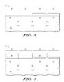
- FIG. 1is a view of a semiconductor device 10 during a processing step.
- Semiconductor device 10may include a semiconductor substrate 12 .
- the semiconductor substrate described hereincan be any semiconductor material or combinations of materials, such as gallium arsenide, silicon germanium, silicon-on-insulator (SOI), silicon, monocrystalline silicon, the like, and combinations of the above.
- trench isolation regions 14 , 16 , and 18may be formed to isolate the different devices to be formed.
- Semiconductor device 10may include an NMOS dual gate oxide (N-DGO) region 20 , an NMOS core (N-Core) region 22 , a PMOS dual gate oxide (P-DGO) region 24 , and a PMOS core (P-Core) region 26 .
- N-DGO region 20 and N-Core region 22may be implanted with boron to form P-well regions (not shown).
- P-DGO region 24 and PMOS-Core region 26may be implanted with arsenic or phosphorus to form N-well regions (not shown).
- NMOS devicesmay be formed in N-DGO region 20 and N-Core region 22 .
- PMOS devicesmay be formed in P-DGO region 24 and P-Core region 26 .
- the devices formed in the dual gate oxide regions ( 20 and 24 )will be formed with thicker gate oxide and the devices formed in the core regions ( 22 and 26 ) will be formed with thinner gate oxide.
- a hard mask 28may be formed over N-DGO region 20 and N-Core region 22 .
- FIG. 2is a view of semiconductor device 10 during a processing step.
- silicon germanium regions 30 and 32may be formed in P-DGO region 24 and P-Core region 26 , respectively.
- silicon germanium regions 30 and 32may be epitaxially grown.
- silicon germanium regions 30 and 32may have a thickness in a range of 30 Angstroms to 150 Angstroms.
- silicon germanium regions 30 and 32may have a thickness in a range of 50 Angstroms to 100 Angstroms.
- silicon germanium regions 30 and 32may have 10% to 50% germanium.
- silicon germanium regions 30 and 32may have 20% to 35% germanium.
- any other semiconductor material that has a different electrical property from semiconductor substrate 12may be used as part of this step.
- silicon carbonmay be used.
- any semiconductor material that changes a band gap of a channel region of a device formed in a region having that semiconductor materialmay be used.
- any semiconductor material that changes a band gap of a channel region of a thick gate device relative to a channel region of a thin gate devicemay be used.
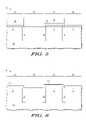
- FIG. 3is a view of semiconductor device 10 during a processing step.
- a high temperature oxide (HTO) layer 34may be formed.
- HTO layer 34may be formed by chemical vapor deposition at a temperature of approximately 800 degree Celsius. The range of temperature may vary from 750 degree Celsius to 900 degree Celsius.
- HTO layer 34may have a thickness in a range of 10 Angstroms to 50 Angstroms. In other embodiments, HTO layer 34 may have a thickness in a range of 20 Angstroms to 30 Angstroms.
- HTO layer 34may be formed using other deposition processes, as well, such as atomic layer deposition, plasma enhanced chemical vapor deposition, and physical vapor deposition.
- FIG. 4is a view of semiconductor device 10 during a processing step.
- patterned resist regions 36may be formed overlying N-DGO region 20 and P-DGO region 24 .
- HTO layer 34may be removed from core regions, including N-Core region 22 and P-Core region 26 leaving portions of HTO layer 34 only in DGO regions.
- lower gate oxide region 38 and lower gate oxide region 40may remain in N-DGO region 20 and P-DGO region 24 .
- HTO layer 34may be removed from N-Core region 22 and P-Core region 26 using a hydrofluoric acid (HF) clean.
- HFhydrofluoric acid
- a diluted HF clean processmay be used.
- patterned resist regions 26may be removed using piranha clean or solvent clean, for example.
- a high k gate oxide layer 42may be formed.
- high k gate oxide layer 42may overlie both core regions and DGO regions.
- high k gate oxide layer 42may directly overlie on lower gate oxide region 38 in N-DGO region 20 , a portion of substrate 12 in N-Core region 22 , lower gate oxide region 40 in P-DGO region 24 , and silicon germanium region 32 in P-Core region 26 .
- high k gate oxide layer 42may be deposited using an atomic layer deposition process. Prior to deposition of high k gate oxide layer 42 , the top surfaces of the relevant regions may be pre-cleaned.
- high k gate oxideincludes any oxide material with k in a range of 10-100. In one embodiment, any oxide material with k in a range of 15-25 may also be used. Suitable materials for forming high k gate oxide layer 42 include hafnium oxide, hafnium silicate, hafnium aluminate, zirconium oxide, zirconium silicate, and other suitable high-k materials. In one embodiment, high-k gate oxide layer 42 may have a thickness in a range of 10 Angstroms to 50 Angstroms. In another embodiment, high-k gate oxide layer 42 may have a thickness in a range of 15 Angstroms to 20 Angstroms.
- metal gate electrode layer 44may be formed overlying high k gate oxide layer 42 .
- metal gate electrode layer 44may contain an element or alloy.
- metal gate electrode layer 44may contain tantalum, titanium, lanthanum, molybdenum, or any combination thereof.
- Metal gate electrode layer 44may further contain carbon and/or nitrogen.
- Metal gate electrode layer 44may be formed using processes, such as atomic layer deposition (ALD), molecular beam deposition (MBD), and chemical vapor deposition (CVD).
- ALDatomic layer deposition
- MBDmolecular beam deposition
- CVDchemical vapor deposition
- metal gate electrode layer 44may have a thickness in a range of 20 Angstroms to 150 Angstroms. In another embodiment, metal gate electrode layer 44 may have thickness in a range of 50 Angstroms to 100 Angstroms.
- a polysilicon gate electrode layer 46may be formed over metal gate electrode layer 44 .
- Polysilicon gate electrode layer 46may be formed using processes, such as atomic layer deposition (ALD), molecular beam deposition (MBD), and chemical vapor deposition (CVD).
- ALDatomic layer deposition
- MBDmolecular beam deposition
- CVDchemical vapor deposition
- polysilicon gate electrode layer 46may have a thickness in a range of 200 Angstroms to 1000 Angstroms. In another embodiment, polysilicon gate electrode layer 46 may have thickness of 500 Angstroms.
- FIG. 8is a view of semiconductor device 10 after formation of PMOS and NMOS devices.
- N-DGO device 50may be formed in N-DGO region 20
- N-Core device 52may be formed in N-Core region 22
- P-DGO device 54may be formed in P-DGO region 24
- P-Core device 56may be formed in P-Core region 26 .
- These devicesmay be formed by forming gate electrodes, spacers, and source/drain regions using conventional semiconductor processing steps.
- N-DGO device 50may include a gate structure including a lower gate oxide region 58 , an upper gate oxide region 60 (formed from the high k gate oxide material), a metal gate electrode region 62 , and a polysilicon gate electrode region 64 .
- N-DGO device 50may further include a spacer 66 formed adjacent to the gate structure.
- N-DGO device 50may further include source/drain regions 68 and 70 .
- N-Core device 52may include a gate structure including a gate oxide region 72 (formed from the high k gate oxide material), a metal gate electrode region 74 , and a polysilicon gate electrode region 76 .
- N-Core device 52may further include a spacer 78 formed adjacent to the gate structure.
- N-Core device 52may further include source/drain regions 80 and 82 .
- P-DGO device 54may include silicon germanium region 30 .
- P-DGO device 54may further include a gate structure including a lower gate oxide region 84 , an upper gate oxide region 86 (formed from the high k gate oxide material), a metal gate electrode region 88 , and a polysilicon gate electrode region 90 .
- P-DGO device 54may further include a spacer 92 formed adjacent to the gate structure.
- P-DGO device 54may further include source/drain regions 94 and 96 .
- P-Core device 56may include silicon germanium region 32 .
- P-Core device 56may further include a gate structure including a gate oxide region 98 (formed from the high k gate oxide material), a metal gate electrode region 100 , and a polysilicon gate electrode region 102 .
- P-Core device 56may further include a spacer 104 formed adjacent to the gate structure.
- P-Core device 56may further include source/drain regions 106 and 108 .
Landscapes
- Metal-Oxide And Bipolar Metal-Oxide Semiconductor Integrated Circuits (AREA)
- Insulated Gate Type Field-Effect Transistor (AREA)
- Thin Film Transistor (AREA)
Abstract
Description
- 1. Field
- This disclosure relates generally to semiconductor devices, and more specifically, to dual gate oxide device integration.
- 2. Related Art
- In many instances, dual gate oxide (DGO) devices need to be integrated on the same substrate. As used herein, the term dual gate oxide devices relates to devices that are formed on the same substrate, but have different gate oxide thicknesses. For example, thicker gate oxide devices may be formed on the periphery of the substrate so that they can handle higher voltages associated with input/output operations. Thinner gate oxide devices may be formed in areas of the substrate where higher voltages are not present. Metal gate with high dielectric constant (high k) devices increasingly need materials that may not be compatible with existing methods for forming dual gate oxide devices. For example, such metal gate/high k dielectric devices may need silicon germanium channels to lower the threshold voltage (Vt) associated with the PMOS devices. Conventional processes, such as thermal oxidation, used to form thick gate oxide devices, however, are not compatible with silicon germanium channels. This is because if thick gate oxide is grown over silicon germanium, the thermal oxidation step results in the germanium diffusing into the regions of the substrate or the gate oxide that should not contain any germanium. In sum, thermal oxidation step used as part of the conventional dual gate oxide integration process may degrade the profile of the silicon germanium channel.
- Accordingly, there is a need for improved dual gate oxide device integration.
- The present invention is illustrated by way of example and is not limited by the accompanying figures, in which like references indicate similar elements. Elements in the figures are illustrated for simplicity and clarity and have not necessarily been drawn to scale.
FIG. 1 is a view of a semiconductor device during a processing step;FIG. 2 is a view of a semiconductor device during a processing step;FIG. 3 is a view of a semiconductor device during a processing step;FIG. 4 is a view of a semiconductor device during a processing step;FIG. 5 is a view of a semiconductor device during a processing step;FIG. 6 is a view of a semiconductor device during a processing step;FIG. 7 is a view of a semiconductor device during a processing step; andFIG. 8 is a view of a semiconductor device during a processing step.- Dual gate oxide device integration is described for transistors including a silicon germanium channel. The use of silicon germanium channel helps in adjusting the threshold voltage of PMOS devices, for example. Silicon carbon channels may be used for NMOS devices, as well.
- In one aspect, a method of forming devices is provided. The method includes forming a first region and a second region in a semiconductor substrate. The method further includes forming a semiconductive material over the first region, wherein the semiconductive material has a different electrical property than the first semiconductor substrate. The method further includes forming a first dielectric material over the first region. The method further includes depositing a second dielectric material over the first dielectric material and over the second region, wherein the second dielectric material is different than the first dielectric material. The method further includes depositing a gate electrode material over the second dielectric material.
- In another aspect, a method of forming devices is provided. The method includes forming a thick gate dielectric device in a first region of a semiconductor substrate, wherein the thick gate dielectric device has a first channel region and the semiconductor substrate comprises a first material. The method further includes forming a thin gate dielectric device in a second region of a semiconductor device, wherein the thin gate dielectric device has a gate dielectric that is thinner than that of the thick gate dielectric, the thin gate dielectric device has a second channel region. Forming the thick gate dielectric device and the thin gate dielectric device further comprises: (1) epitaxially growing the first channel region over the first region, wherein the first channel region comprises a second material, wherein the second material is different from the first material; (2) forming a first gate dielectric over the first channel region; (3) forming a second gate dielectric over the first gate dielectric and the second region; and (4) depositing a gate electrode material over the second gate dielectric.
- In yet another aspect, a method including forming an isolation region in a semiconductor substrate to form a first semiconductor region and a second semiconductive region in a semiconductor substrate is provided. The method further includes epitaxially growing a semiconductive material over the first semiconductive region, wherein the semiconductive material comprises an element selected from the group consisting of germanium and carbon. The method further includes depositing a first dielectric material over the first semiconductive region. The method further includes depositing a second dielectric material over the first dielectric material and the second semiconductive region. The method further includes depositing a gate electrode material over the second dielectric material.
FIG. 1 is a view of asemiconductor device 10 during a processing step.Semiconductor device 10 may include asemiconductor substrate 12. The semiconductor substrate described herein can be any semiconductor material or combinations of materials, such as gallium arsenide, silicon germanium, silicon-on-insulator (SOI), silicon, monocrystalline silicon, the like, and combinations of the above. Withinsubstrate 12,trench isolation regions Semiconductor device 10 may include an NMOS dual gate oxide (N-DGO)region 20, an NMOS core (N-Core)region 22, a PMOS dual gate oxide (P-DGO)region 24, and a PMOS core (P-Core)region 26. N-DGOregion 20 and N-Coreregion 22 may be implanted with boron to form P-well regions (not shown). P-DGO region 24 and PMOS-Core region 26 may be implanted with arsenic or phosphorus to form N-well regions (not shown). NMOS devices may be formed in N-DGOregion 20 and N-Coreregion 22. PMOS devices may be formed in P-DGOregion 24 and P-Coreregion 26. The devices formed in the dual gate oxide regions (20 and24) will be formed with thicker gate oxide and the devices formed in the core regions (22 and26) will be formed with thinner gate oxide. Next, as shown inFIG. 1 , ahard mask 28 may be formed over N-DGOregion 20 and N-Coreregion 22.FIG. 2 is a view ofsemiconductor device 10 during a processing step. As part of this processing step,silicon germanium regions DGO region 24 and P-Coreregion 26, respectively. In one embodiment,silicon germanium regions silicon germanium regions silicon germanium regions silicon germanium regions silicon germanium regions semiconductor substrate 12 may be used as part of this step. For example, in one embodiment, silicon carbon may be used. In one embodiment, any semiconductor material that changes a band gap of a channel region of a device formed in a region having that semiconductor material may be used. In another embodiment, any semiconductor material that changes a band gap of a channel region of a thick gate device relative to a channel region of a thin gate device may be used.FIG. 3 is a view ofsemiconductor device 10 during a processing step. As part of this processing step, a high temperature oxide (HTO)layer 34 may be formed. In one embodiment,HTO layer 34 may be formed by chemical vapor deposition at a temperature of approximately 800 degree Celsius. The range of temperature may vary from 750 degree Celsius to 900 degree Celsius. By way of example,HTO layer 34 may have a thickness in a range of 10 Angstroms to 50 Angstroms. In other embodiments,HTO layer 34 may have a thickness in a range of 20 Angstroms to 30 Angstroms.HTO layer 34 may be formed using other deposition processes, as well, such as atomic layer deposition, plasma enhanced chemical vapor deposition, and physical vapor deposition.FIG. 4 is a view ofsemiconductor device 10 during a processing step. As part of this processing step, patterned resistregions 36 may be formed overlying N-DGO region 20 and P-DGO region 24.- Next, as shown in
FIG. 5 , using patterned resistregions 36,HTO layer 34 may be removed from core regions, including N-Core region 22 and P-Core region 26 leaving portions ofHTO layer 34 only in DGO regions. Thus, for example, lowergate oxide region 38 and lowergate oxide region 40 may remain in N-DGO region 20 and P-DGO region 24. In one embodiment,HTO layer 34 may be removed from N-Core region 22 and P-Core region 26 using a hydrofluoric acid (HF) clean. In one embodiment, a diluted HF clean process may be used. Having removed HTO layer from N-Core region 22 and P-Core region 26, patterned resistregions 26 may be removed using piranha clean or solvent clean, for example. - Next, as shown in
FIG. 6 , a high kgate oxide layer 42 may be formed. In one embodiment, high kgate oxide layer 42 may overlie both core regions and DGO regions. Thus, for example, high kgate oxide layer 42 may directly overlie on lowergate oxide region 38 in N-DGO region 20, a portion ofsubstrate 12 in N-Core region 22, lowergate oxide region 40 in P-DGO region 24, andsilicon germanium region 32 in P-Core region 26. In one embodiment, high kgate oxide layer 42 may be deposited using an atomic layer deposition process. Prior to deposition of high kgate oxide layer 42, the top surfaces of the relevant regions may be pre-cleaned. As used herein the term high k gate oxide includes any oxide material with k in a range of 10-100. In one embodiment, any oxide material with k in a range of 15-25 may also be used. Suitable materials for forming high kgate oxide layer 42 include hafnium oxide, hafnium silicate, hafnium aluminate, zirconium oxide, zirconium silicate, and other suitable high-k materials. In one embodiment, high-kgate oxide layer 42 may have a thickness in a range of 10 Angstroms to 50 Angstroms. In another embodiment, high-kgate oxide layer 42 may have a thickness in a range of 15 Angstroms to 20 Angstroms. - Next, as shown in
FIG. 7 , a metalgate electrode layer 44 may be formed overlying high kgate oxide layer 42. In one embodiment, metalgate electrode layer 44 may contain an element or alloy. By way of example, metalgate electrode layer 44 may contain tantalum, titanium, lanthanum, molybdenum, or any combination thereof. Metalgate electrode layer 44 may further contain carbon and/or nitrogen. Metalgate electrode layer 44 may be formed using processes, such as atomic layer deposition (ALD), molecular beam deposition (MBD), and chemical vapor deposition (CVD). By way of example, metalgate electrode layer 44 may have a thickness in a range of 20 Angstroms to 150 Angstroms. In another embodiment, metalgate electrode layer 44 may have thickness in a range of 50 Angstroms to 100 Angstroms. - Referring still to
FIG. 7 , after formation of metalgate electrode layer 44, a polysilicongate electrode layer 46 may be formed over metalgate electrode layer 44. Polysilicongate electrode layer 46 may be formed using processes, such as atomic layer deposition (ALD), molecular beam deposition (MBD), and chemical vapor deposition (CVD). By way of example, polysilicongate electrode layer 46 may have a thickness in a range of 200 Angstroms to 1000 Angstroms. In another embodiment, polysilicongate electrode layer 46 may have thickness of 500 Angstroms. FIG. 8 is a view ofsemiconductor device 10 after formation of PMOS and NMOS devices. By way of example, N-DGO device 50 may be formed in N-DGO region 20, N-Core device 52 may be formed in N-Core region 22, P-DGO device 54 may be formed in P-DGO region 24, and P-Core device 56 may be formed in P-Core region 26. These devices may be formed by forming gate electrodes, spacers, and source/drain regions using conventional semiconductor processing steps. Thus, for example, N-DGO device 50 may include a gate structure including a lowergate oxide region 58, an upper gate oxide region60 (formed from the high k gate oxide material), a metalgate electrode region 62, and a polysilicongate electrode region 64. N-DGO device 50 may further include aspacer 66 formed adjacent to the gate structure. N-DGO device 50 may further include source/drain regions Core device 52 may include a gate structure including a gate oxide region72 (formed from the high k gate oxide material), a metalgate electrode region 74, and a polysilicongate electrode region 76. N-Core device 52 may further include aspacer 78 formed adjacent to the gate structure. N-Core device 52 may further include source/drain regions DGO device 54 may includesilicon germanium region 30. P-DGO device 54 may further include a gate structure including a lowergate oxide region 84, an upper gate oxide region86 (formed from the high k gate oxide material), a metalgate electrode region 88, and a polysilicongate electrode region 90. P-DGO device 54 may further include aspacer 92 formed adjacent to the gate structure. P-DGO device 54 may further include source/drain regions Core device 56 may includesilicon germanium region 32. P-Core device 56 may further include a gate structure including a gate oxide region98 (formed from the high k gate oxide material), a metalgate electrode region 100, and a polysilicongate electrode region 102. P-Core device 56 may further include aspacer 104 formed adjacent to the gate structure. P-Core device 56 may further include source/drain regions - Although the invention has been described with respect to specific conductivity types or polarity of potentials, skilled artisans appreciated that conductivity types and polarities of potentials may be reversed. Thus, for example, although the process flow is described above with respect to PMOS devices having silicon germanium regions, a similar process flow may be used with NMOS devices having silicon carbon.
- Moreover, the terms “front,” “back,” “top,” “bottom,” “over,” “under” and the like in the description and in the claims, if any, are used for descriptive purposes and not necessarily for describing permanent relative positions. It is understood that the terms so used are interchangeable under appropriate circumstances such that the embodiments of the invention described herein are, for example, capable of operation in other orientations than those illustrated or otherwise described herein.
- Although the invention is described herein with reference to specific embodiments, various modifications and changes can be made without departing from the scope of the present invention as set forth in the claims below. Accordingly, the specification and figures are to be regarded in an illustrative rather than a restrictive sense, and all such modifications are intended to be included within the scope of the present invention. Any benefits, advantages, or solutions to problems that are described herein with regard to specific embodiments are not intended to be construed as a critical, required, or essential feature or element of any or all the claims.
- Furthermore, the terms “a” or “an,” as used herein, are defined as one or more than one. Also, the use of introductory phrases such as “at least one” and “one or more” in the claims should not be construed to imply that the introduction of another claim element by the indefinite articles “a” or “an” limits any particular claim containing such introduced claim element to inventions containing only one such element, even when the same claim includes the introductory phrases “one or more” or “at least one” and indefinite articles such as “a” or “an.” The same holds true for the use of definite articles.
- Unless stated otherwise, terms such as “first” and “second” are used to arbitrarily distinguish between the elements such terms describe. Thus, these terms are not necessarily intended to indicate temporal or other prioritization of such elements.
Claims (20)
Priority Applications (6)
| Application Number | Priority Date | Filing Date | Title |
|---|---|---|---|
| US11/851,719US7709331B2 (en) | 2007-09-07 | 2007-09-07 | Dual gate oxide device integration |
| EP08782025AEP2191504A4 (en) | 2007-09-07 | 2008-07-18 | DOUBLE-gate oxide ARRANGEMENT INTEGRATION |
| JP2010524070AJP2010538496A (en) | 2007-09-07 | 2008-07-18 | Integration of double gate oxide devices |
| CN2008801057207ACN101796631B (en) | 2007-09-07 | 2008-07-18 | Dual gate oxide device integration |
| PCT/US2008/070404WO2009032411A1 (en) | 2007-09-07 | 2008-07-18 | Dual gate oxide device integration |
| TW097129047ATWI453823B (en) | 2007-09-07 | 2008-07-31 | Double gate electrode oxide device integration |
Applications Claiming Priority (1)
| Application Number | Priority Date | Filing Date | Title |
|---|---|---|---|
| US11/851,719US7709331B2 (en) | 2007-09-07 | 2007-09-07 | Dual gate oxide device integration |
Publications (2)
| Publication Number | Publication Date |
|---|---|
| US20090068807A1true US20090068807A1 (en) | 2009-03-12 |
| US7709331B2 US7709331B2 (en) | 2010-05-04 |
Family
ID=40429260
Family Applications (1)
| Application Number | Title | Priority Date | Filing Date |
|---|---|---|---|
| US11/851,719Active2028-10-21US7709331B2 (en) | 2007-09-07 | 2007-09-07 | Dual gate oxide device integration |
Country Status (6)
| Country | Link |
|---|---|
| US (1) | US7709331B2 (en) |
| EP (1) | EP2191504A4 (en) |
| JP (1) | JP2010538496A (en) |
| CN (1) | CN101796631B (en) |
| TW (1) | TWI453823B (en) |
| WO (1) | WO2009032411A1 (en) |
Cited By (11)
| Publication number | Priority date | Publication date | Assignee | Title |
|---|---|---|---|---|
| US20100151693A1 (en)* | 2008-12-16 | 2010-06-17 | Takashi Shimizu | Method for manufacturing semiconductor device comprising mutioxide |
| US20100308418A1 (en)* | 2009-06-09 | 2010-12-09 | Knut Stahrenberg | Semiconductor Devices and Methods of Manufacture Thereof |
| US20110042751A1 (en)* | 2009-08-18 | 2011-02-24 | International Business Machines Corporation | Thermal dual gate oxide device integration |
| JP2011066406A (en)* | 2009-09-18 | 2011-03-31 | Internatl Business Mach Corp <Ibm> | METAL GATE AND HIGH-k DIELECTRIC DEVICE WITH PFET CHANNEL SiGe |
| WO2011112611A1 (en) | 2010-03-09 | 2011-09-15 | Valspar Sourcing, Inc. | Non-blooming low formaldehyde coating composition |
| US20110254106A1 (en)* | 2010-04-16 | 2011-10-20 | Fujitsu Semiconductor Limited | Semiconductor device and semiconductor device manufacturing method |
| US20120295420A1 (en)* | 2011-05-20 | 2012-11-22 | Globalfoundries Inc. | Semiconductor devices with reduced sti topography by using chemical oxide removal |
| US8482077B2 (en) | 2010-05-07 | 2013-07-09 | Samsung Electronics Co., Ltd. | Semiconductor devices and methods for fabricating the same |
| US20140035064A1 (en)* | 2012-08-03 | 2014-02-06 | International Business Machines Corporation | Semiconductor structures and methods of manufacture |
| US20140342565A1 (en)* | 2013-05-14 | 2014-11-20 | Shanghai Huali Microelectronics Corporation | Method of manufacturing dual gate oxide devices |
| US10665585B2 (en)* | 2010-05-19 | 2020-05-26 | Taiwan Semiconductor Manufacturing Company, Ltd. | Structure and method for alignment marks |
Families Citing this family (14)
| Publication number | Priority date | Publication date | Assignee | Title |
|---|---|---|---|---|
| DE102008063402B4 (en)* | 2008-12-31 | 2013-10-17 | Advanced Micro Devices, Inc. | Reducing the threshold voltage fluctuation in transistors with a channel semiconductor alloy by reducing the deposition nonuniformities |
| US8017469B2 (en) | 2009-01-21 | 2011-09-13 | Freescale Semiconductor, Inc. | Dual high-k oxides with sige channel |
| US7943460B2 (en)* | 2009-04-20 | 2011-05-17 | International Business Machines Corporation | High-K metal gate CMOS |
| US8114739B2 (en)* | 2009-09-28 | 2012-02-14 | Freescale Semiconductor, Inc. | Semiconductor device with oxygen-diffusion barrier layer and method for fabricating same |
| JP5605134B2 (en)* | 2010-09-30 | 2014-10-15 | 富士通セミコンダクター株式会社 | Semiconductor device and manufacturing method thereof |
| US8304306B2 (en)* | 2011-03-28 | 2012-11-06 | International Business Machines Corporation | Fabrication of devices having different interfacial oxide thickness via lateral oxidation |
| CN103165533A (en)* | 2013-03-15 | 2013-06-19 | 上海华力微电子有限公司 | Process method for preventing defects of photoresist during wet etching |
| CN103258794A (en)* | 2013-03-15 | 2013-08-21 | 上海华力微电子有限公司 | Technological method capable of preventing shortcomings on photoresist during wet etching |
| CN103199016A (en)* | 2013-03-15 | 2013-07-10 | 上海华力微电子有限公司 | Process method for preventing occurrence of defects of photoresist in wet etching |
| CN103258733A (en)* | 2013-03-15 | 2013-08-21 | 上海华力微电子有限公司 | Technological method capable of preventing shortcomings on photoresist during wet etching |
| CN103258795A (en)* | 2013-03-15 | 2013-08-21 | 上海华力微电子有限公司 | Technological method capable of preventing shortcomings on photoresist during wet etching |
| US9373501B2 (en)* | 2013-04-16 | 2016-06-21 | International Business Machines Corporation | Hydroxyl group termination for nucleation of a dielectric metallic oxide |
| CN103293848B (en)* | 2013-05-23 | 2015-12-23 | 上海华力微电子有限公司 | The disposal route of photoresist and the preparation method of semiconductor devices |
| US10002939B1 (en) | 2017-02-16 | 2018-06-19 | International Business Machines Corporation | Nanosheet transistors having thin and thick gate dielectric material |
Citations (13)
| Publication number | Priority date | Publication date | Assignee | Title |
|---|---|---|---|---|
| US6541357B1 (en)* | 2001-12-04 | 2003-04-01 | Kabushiki Kaisha Toshiba | Semiconductor device and method of manufacturing the same |
| US6620664B2 (en)* | 2002-02-07 | 2003-09-16 | Sharp Laboratories Of America, Inc. | Silicon-germanium MOSFET with deposited gate dielectric and metal gate electrode and method for making the same |
| US20040005749A1 (en)* | 2002-07-02 | 2004-01-08 | Choi Gil-Heyun | Methods of forming dual gate semiconductor devices having a metal nitride layer |
| US20040032001A1 (en)* | 2002-08-15 | 2004-02-19 | Gilmer David C. | Method for forming a dual gate oxide device using a metal oxide and resulting device |
| US20040038538A1 (en)* | 2002-08-23 | 2004-02-26 | Tuo-Hung Ho | Dual-gate structure and method of fabricating integrated circuits having dual-gate structures |
| US6730576B1 (en)* | 2002-12-31 | 2004-05-04 | Advanced Micro Devices, Inc. | Method of forming a thick strained silicon layer and semiconductor structures incorporating a thick strained silicon layer |
| US6830962B1 (en)* | 2003-08-05 | 2004-12-14 | International Business Machines Corporation | Self-aligned SOI with different crystal orientation using wafer bonding and SIMOX processes |
| US20050280097A1 (en)* | 2004-06-21 | 2005-12-22 | Anderson Brent A | Dual gate dielectric thickness devices |
| US20050285192A1 (en)* | 2004-06-29 | 2005-12-29 | International Business Machines Corporation | Structures and methods for manufacturing p-type mosfet withgraded embedded silicon-germanium source-drain and/or extension |
| US6982230B2 (en)* | 2002-11-08 | 2006-01-03 | International Business Machines Corporation | Deposition of hafnium oxide and/or zirconium oxide and fabrication of passivated electronic structures |
| US20060081948A1 (en)* | 2004-10-19 | 2006-04-20 | Ha-Jin Lim | Transistors with multilayered dielectric films and methods of manufacturing such transistors |
| US7101746B2 (en)* | 2003-11-05 | 2006-09-05 | Chartered Semiconductor Manufacturing Ltd. | Method to lower work function of gate electrode through Ge implantation |
| US20070023817A1 (en)* | 2005-07-28 | 2007-02-01 | Dao Thuy B | Structure and manufacturing method of multi-gate dielectric thicknesses for planar double gate device having multi-threshold voltages |
Family Cites Families (9)
| Publication number | Priority date | Publication date | Assignee | Title |
|---|---|---|---|---|
| JPH0590517A (en)* | 1991-09-30 | 1993-04-09 | Toshiba Corp | Semiconductor device and manufacture thereof |
| JPH10135450A (en)* | 1996-10-31 | 1998-05-22 | Sumitomo Metal Ind Ltd | Field effect transistor and method for manufacturing the same |
| US6518106B2 (en)* | 2001-05-26 | 2003-02-11 | Motorola, Inc. | Semiconductor device and a method therefor |
| CN100334732C (en)* | 2001-11-30 | 2007-08-29 | 株式会社瑞萨科技 | Semiconductor integrated circuit device and its mfg. method |
| US6620656B2 (en) | 2001-12-19 | 2003-09-16 | Motorola, Inc. | Method of forming body-tied silicon on insulator semiconductor device |
| US7229893B2 (en)* | 2004-06-23 | 2007-06-12 | Taiwan Semiconductor Manufacturing Company, Ltd. | Method and apparatus for a semiconductor device with a high-k gate dielectric |
| US7364969B2 (en)* | 2005-07-01 | 2008-04-29 | Freescale Semiconductor, Inc. | Semiconductor fabrication process for integrating formation of embedded nonvolatile storage device with formation of multiple transistor device types |
| US7524707B2 (en)* | 2005-08-23 | 2009-04-28 | Freescale Semiconductor, Inc. | Modified hybrid orientation technology |
| TWI267926B (en)* | 2005-09-23 | 2006-12-01 | Ind Tech Res Inst | A new method for high mobility enhancement strained channel CMOS with single workfunction metal-gate |
- 2007
- 2007-09-07USUS11/851,719patent/US7709331B2/enactiveActive
- 2008
- 2008-07-18CNCN2008801057207Apatent/CN101796631B/ennot_activeExpired - Fee Related
- 2008-07-18JPJP2010524070Apatent/JP2010538496A/enactivePending
- 2008-07-18WOPCT/US2008/070404patent/WO2009032411A1/enactiveApplication Filing
- 2008-07-18EPEP08782025Apatent/EP2191504A4/ennot_activeWithdrawn
- 2008-07-31TWTW097129047Apatent/TWI453823B/ennot_activeIP Right Cessation
Patent Citations (17)
| Publication number | Priority date | Publication date | Assignee | Title |
|---|---|---|---|---|
| US6541357B1 (en)* | 2001-12-04 | 2003-04-01 | Kabushiki Kaisha Toshiba | Semiconductor device and method of manufacturing the same |
| US6620664B2 (en)* | 2002-02-07 | 2003-09-16 | Sharp Laboratories Of America, Inc. | Silicon-germanium MOSFET with deposited gate dielectric and metal gate electrode and method for making the same |
| US20040005749A1 (en)* | 2002-07-02 | 2004-01-08 | Choi Gil-Heyun | Methods of forming dual gate semiconductor devices having a metal nitride layer |
| US6787421B2 (en)* | 2002-08-15 | 2004-09-07 | Freescale Semiconductor, Inc. | Method for forming a dual gate oxide device using a metal oxide and resulting device |
| US20040032001A1 (en)* | 2002-08-15 | 2004-02-19 | Gilmer David C. | Method for forming a dual gate oxide device using a metal oxide and resulting device |
| US20040038538A1 (en)* | 2002-08-23 | 2004-02-26 | Tuo-Hung Ho | Dual-gate structure and method of fabricating integrated circuits having dual-gate structures |
| US20060138603A1 (en)* | 2002-11-08 | 2006-06-29 | International Business Machines Corporation | Deposition of hafnium oxide and/or zirconium oxide and fabrication of passivated electronic structures |
| US6982230B2 (en)* | 2002-11-08 | 2006-01-03 | International Business Machines Corporation | Deposition of hafnium oxide and/or zirconium oxide and fabrication of passivated electronic structures |
| US6730576B1 (en)* | 2002-12-31 | 2004-05-04 | Advanced Micro Devices, Inc. | Method of forming a thick strained silicon layer and semiconductor structures incorporating a thick strained silicon layer |
| US6830962B1 (en)* | 2003-08-05 | 2004-12-14 | International Business Machines Corporation | Self-aligned SOI with different crystal orientation using wafer bonding and SIMOX processes |
| US7101746B2 (en)* | 2003-11-05 | 2006-09-05 | Chartered Semiconductor Manufacturing Ltd. | Method to lower work function of gate electrode through Ge implantation |
| US20050280097A1 (en)* | 2004-06-21 | 2005-12-22 | Anderson Brent A | Dual gate dielectric thickness devices |
| US7087470B2 (en)* | 2004-06-21 | 2006-08-08 | International Business Machines Corporation | Dual gate dielectric thickness devices |
| US20060208323A1 (en)* | 2004-06-21 | 2006-09-21 | International Business Machines Corporation | Dual gate dielectric thickness devices |
| US20050285192A1 (en)* | 2004-06-29 | 2005-12-29 | International Business Machines Corporation | Structures and methods for manufacturing p-type mosfet withgraded embedded silicon-germanium source-drain and/or extension |
| US20060081948A1 (en)* | 2004-10-19 | 2006-04-20 | Ha-Jin Lim | Transistors with multilayered dielectric films and methods of manufacturing such transistors |
| US20070023817A1 (en)* | 2005-07-28 | 2007-02-01 | Dao Thuy B | Structure and manufacturing method of multi-gate dielectric thicknesses for planar double gate device having multi-threshold voltages |
Cited By (17)
| Publication number | Priority date | Publication date | Assignee | Title |
|---|---|---|---|---|
| US20100151693A1 (en)* | 2008-12-16 | 2010-06-17 | Takashi Shimizu | Method for manufacturing semiconductor device comprising mutioxide |
| US20100308418A1 (en)* | 2009-06-09 | 2010-12-09 | Knut Stahrenberg | Semiconductor Devices and Methods of Manufacture Thereof |
| US20110042751A1 (en)* | 2009-08-18 | 2011-02-24 | International Business Machines Corporation | Thermal dual gate oxide device integration |
| US8105892B2 (en) | 2009-08-18 | 2012-01-31 | International Business Machines Corporation | Thermal dual gate oxide device integration |
| JP2011066406A (en)* | 2009-09-18 | 2011-03-31 | Internatl Business Mach Corp <Ibm> | METAL GATE AND HIGH-k DIELECTRIC DEVICE WITH PFET CHANNEL SiGe |
| WO2011112611A1 (en) | 2010-03-09 | 2011-09-15 | Valspar Sourcing, Inc. | Non-blooming low formaldehyde coating composition |
| US20110254106A1 (en)* | 2010-04-16 | 2011-10-20 | Fujitsu Semiconductor Limited | Semiconductor device and semiconductor device manufacturing method |
| US8786022B2 (en)* | 2010-04-16 | 2014-07-22 | Fujitsu Semiconductor Limited | Semiconductor device and semiconductor device manufacturing method |
| US8482077B2 (en) | 2010-05-07 | 2013-07-09 | Samsung Electronics Co., Ltd. | Semiconductor devices and methods for fabricating the same |
| US10665585B2 (en)* | 2010-05-19 | 2020-05-26 | Taiwan Semiconductor Manufacturing Company, Ltd. | Structure and method for alignment marks |
| US11121128B2 (en) | 2010-05-19 | 2021-09-14 | Taiwan Semiconductor Manufacturing Company, Ltd. | Structure and method for alignment marks |
| US20120295420A1 (en)* | 2011-05-20 | 2012-11-22 | Globalfoundries Inc. | Semiconductor devices with reduced sti topography by using chemical oxide removal |
| US20140035064A1 (en)* | 2012-08-03 | 2014-02-06 | International Business Machines Corporation | Semiconductor structures and methods of manufacture |
| US8916440B2 (en)* | 2012-08-03 | 2014-12-23 | International Business Machines Corporation | Semiconductor structures and methods of manufacture |
| US9356014B2 (en) | 2012-08-03 | 2016-05-31 | Globalfoundries Inc. | High-voltage metal-insulator-semiconductor field effect transistor structures |
| US20140342565A1 (en)* | 2013-05-14 | 2014-11-20 | Shanghai Huali Microelectronics Corporation | Method of manufacturing dual gate oxide devices |
| US8962494B2 (en)* | 2013-05-14 | 2015-02-24 | Shanghai Huali Microelectronics Corporation | Method of manufacturing dual gate oxide devices |
Also Published As
| Publication number | Publication date |
|---|---|
| JP2010538496A (en) | 2010-12-09 |
| EP2191504A1 (en) | 2010-06-02 |
| TW200921787A (en) | 2009-05-16 |
| US7709331B2 (en) | 2010-05-04 |
| CN101796631B (en) | 2012-09-26 |
| EP2191504A4 (en) | 2012-09-05 |
| CN101796631A (en) | 2010-08-04 |
| WO2009032411A1 (en) | 2009-03-12 |
| TWI453823B (en) | 2014-09-21 |
Similar Documents
| Publication | Publication Date | Title |
|---|---|---|
| US7709331B2 (en) | Dual gate oxide device integration | |
| US8017469B2 (en) | Dual high-k oxides with sige channel | |
| US8507991B2 (en) | Semiconductor device and method of manufacturing the same | |
| US8114739B2 (en) | Semiconductor device with oxygen-diffusion barrier layer and method for fabricating same | |
| US9054130B2 (en) | Bottle-neck recess in a semiconductor device | |
| US8860150B2 (en) | Metal gate structure | |
| US20120003798A1 (en) | Replacement gates to enhance transistor strain | |
| CN102203924A (en) | Optimized compressive sige channel pmos transistor with engineered ge profile and optimized silicon cap layer | |
| US8835260B2 (en) | Control of threshold voltages in high-k metal gate stack and structures for CMOS devices | |
| KR101811713B1 (en) | Methods of forming cmos transistors using tensile stress layers and hydrogen plasma treatment | |
| JP2010177240A (en) | Semiconductor device and method of manufacturing the same | |
| CN1996617A (en) | Semiconductor device and method of manufacturing the same | |
| US7833852B2 (en) | Source/drain stressors formed using in-situ epitaxial growth | |
| US10312084B2 (en) | Semiconductor device and fabrication method thereof | |
| US20120261674A1 (en) | Semiconductor device and method for forming the same | |
| US7799668B2 (en) | Formation of uniform silicate gate dielectrics |
Legal Events
| Date | Code | Title | Description |
|---|---|---|---|
| AS | Assignment | Owner name:FREESCALE SEMICONDUCTOR, INC., TEXAS Free format text:ASSIGNMENT OF ASSIGNORS INTEREST;ASSIGNORS:KARVE, GAURI V.;SAMAVEDAM, SRIKANTH B.;TAYLOR, WILLIAM J., JR.;REEL/FRAME:019798/0220;SIGNING DATES FROM 20070829 TO 20070831 Owner name:FREESCALE SEMICONDUCTOR, INC.,TEXAS Free format text:ASSIGNMENT OF ASSIGNORS INTEREST;ASSIGNORS:KARVE, GAURI V.;SAMAVEDAM, SRIKANTH B.;TAYLOR, WILLIAM J., JR.;SIGNING DATES FROM 20070829 TO 20070831;REEL/FRAME:019798/0220 | |
| AS | Assignment | Owner name:CITIBANK, N.A., NEW YORK Free format text:SECURITY AGREEMENT;ASSIGNOR:FREESCALE SEMICONDUCTOR, INC.;REEL/FRAME:020518/0215 Effective date:20071025 Owner name:CITIBANK, N.A.,NEW YORK Free format text:SECURITY AGREEMENT;ASSIGNOR:FREESCALE SEMICONDUCTOR, INC.;REEL/FRAME:020518/0215 Effective date:20071025 | |
| AS | Assignment | Owner name:CITIBANK, N.A.,NEW YORK Free format text:SECURITY AGREEMENT;ASSIGNOR:FREESCALE SEMICONDUCTOR, INC.;REEL/FRAME:024085/0001 Effective date:20100219 Owner name:CITIBANK, N.A., NEW YORK Free format text:SECURITY AGREEMENT;ASSIGNOR:FREESCALE SEMICONDUCTOR, INC.;REEL/FRAME:024085/0001 Effective date:20100219 | |
| STCF | Information on status: patent grant | Free format text:PATENTED CASE | |
| AS | Assignment | Owner name:CITIBANK, N.A., AS COLLATERAL AGENT,NEW YORK Free format text:SECURITY AGREEMENT;ASSIGNOR:FREESCALE SEMICONDUCTOR, INC.;REEL/FRAME:024397/0001 Effective date:20100413 Owner name:CITIBANK, N.A., AS COLLATERAL AGENT, NEW YORK Free format text:SECURITY AGREEMENT;ASSIGNOR:FREESCALE SEMICONDUCTOR, INC.;REEL/FRAME:024397/0001 Effective date:20100413 | |
| AS | Assignment | Owner name:CITIBANK, N.A., AS NOTES COLLATERAL AGENT, NEW YORK Free format text:SECURITY AGREEMENT;ASSIGNOR:FREESCALE SEMICONDUCTOR, INC.;REEL/FRAME:030633/0424 Effective date:20130521 Owner name:CITIBANK, N.A., AS NOTES COLLATERAL AGENT, NEW YOR Free format text:SECURITY AGREEMENT;ASSIGNOR:FREESCALE SEMICONDUCTOR, INC.;REEL/FRAME:030633/0424 Effective date:20130521 | |
| FPAY | Fee payment | Year of fee payment:4 | |
| AS | Assignment | Owner name:CITIBANK, N.A., AS NOTES COLLATERAL AGENT, NEW YORK Free format text:SECURITY AGREEMENT;ASSIGNOR:FREESCALE SEMICONDUCTOR, INC.;REEL/FRAME:031591/0266 Effective date:20131101 Owner name:CITIBANK, N.A., AS NOTES COLLATERAL AGENT, NEW YOR Free format text:SECURITY AGREEMENT;ASSIGNOR:FREESCALE SEMICONDUCTOR, INC.;REEL/FRAME:031591/0266 Effective date:20131101 | |
| AS | Assignment | Owner name:FREESCALE SEMICONDUCTOR, INC., TEXAS Free format text:PATENT RELEASE;ASSIGNOR:CITIBANK, N.A., AS COLLATERAL AGENT;REEL/FRAME:037356/0143 Effective date:20151207 Owner name:FREESCALE SEMICONDUCTOR, INC., TEXAS Free format text:PATENT RELEASE;ASSIGNOR:CITIBANK, N.A., AS COLLATERAL AGENT;REEL/FRAME:037354/0704 Effective date:20151207 Owner name:FREESCALE SEMICONDUCTOR, INC., TEXAS Free format text:PATENT RELEASE;ASSIGNOR:CITIBANK, N.A., AS COLLATERAL AGENT;REEL/FRAME:037356/0553 Effective date:20151207 | |
| AS | Assignment | Owner name:MORGAN STANLEY SENIOR FUNDING, INC., MARYLAND Free format text:ASSIGNMENT AND ASSUMPTION OF SECURITY INTEREST IN PATENTS;ASSIGNOR:CITIBANK, N.A.;REEL/FRAME:037486/0517 Effective date:20151207 | |
| AS | Assignment | Owner name:MORGAN STANLEY SENIOR FUNDING, INC., MARYLAND Free format text:ASSIGNMENT AND ASSUMPTION OF SECURITY INTEREST IN PATENTS;ASSIGNOR:CITIBANK, N.A.;REEL/FRAME:037518/0292 Effective date:20151207 | |
| AS | Assignment | Owner name:NORTH STAR INNOVATIONS INC., CALIFORNIA Free format text:ASSIGNMENT OF ASSIGNORS INTEREST;ASSIGNOR:FREESCALE SEMICONDUCTOR, INC.;REEL/FRAME:037694/0264 Effective date:20151002 | |
| AS | Assignment | Owner name:NXP, B.V., F/K/A FREESCALE SEMICONDUCTOR, INC., NETHERLANDS Free format text:RELEASE BY SECURED PARTY;ASSIGNOR:MORGAN STANLEY SENIOR FUNDING, INC.;REEL/FRAME:040925/0001 Effective date:20160912 Owner name:NXP, B.V., F/K/A FREESCALE SEMICONDUCTOR, INC., NE Free format text:RELEASE BY SECURED PARTY;ASSIGNOR:MORGAN STANLEY SENIOR FUNDING, INC.;REEL/FRAME:040925/0001 Effective date:20160912 | |
| AS | Assignment | Owner name:NXP B.V., NETHERLANDS Free format text:RELEASE BY SECURED PARTY;ASSIGNOR:MORGAN STANLEY SENIOR FUNDING, INC.;REEL/FRAME:040928/0001 Effective date:20160622 | |
| AS | Assignment | Owner name:MORGAN STANLEY SENIOR FUNDING, INC., MARYLAND Free format text:CORRECTIVE ASSIGNMENT TO CORRECT THE REMOVE PATENTS 8108266 AND 8062324 AND REPLACE THEM WITH 6108266 AND 8060324 PREVIOUSLY RECORDED ON REEL 037518 FRAME 0292. ASSIGNOR(S) HEREBY CONFIRMS THE ASSIGNMENT AND ASSUMPTION OF SECURITY INTEREST IN PATENTS;ASSIGNOR:CITIBANK, N.A.;REEL/FRAME:041703/0536 Effective date:20151207 | |
| MAFP | Maintenance fee payment | Free format text:PAYMENT OF MAINTENANCE FEE, 8TH YEAR, LARGE ENTITY (ORIGINAL EVENT CODE: M1552) Year of fee payment:8 | |
| AS | Assignment | Owner name:SHENZHEN XINGUODU TECHNOLOGY CO., LTD., CHINA Free format text:CORRECTIVE ASSIGNMENT TO CORRECT THE TO CORRECT THE APPLICATION NO. FROM 13,883,290 TO 13,833,290 PREVIOUSLY RECORDED ON REEL 041703 FRAME 0536. ASSIGNOR(S) HEREBY CONFIRMS THE THE ASSIGNMENT AND ASSUMPTION OF SECURITYINTEREST IN PATENTS.;ASSIGNOR:MORGAN STANLEY SENIOR FUNDING, INC.;REEL/FRAME:048734/0001 Effective date:20190217 | |
| AS | Assignment | Owner name:MORGAN STANLEY SENIOR FUNDING, INC., MARYLAND Free format text:CORRECTIVE ASSIGNMENT TO CORRECT THE REMOVE APPLICATION11759915 AND REPLACE IT WITH APPLICATION 11759935 PREVIOUSLY RECORDED ON REEL 037486 FRAME 0517. ASSIGNOR(S) HEREBY CONFIRMS THE ASSIGNMENT AND ASSUMPTION OF SECURITYINTEREST IN PATENTS;ASSIGNOR:CITIBANK, N.A.;REEL/FRAME:053547/0421 Effective date:20151207 | |
| AS | Assignment | Owner name:NXP B.V., NETHERLANDS Free format text:CORRECTIVE ASSIGNMENT TO CORRECT THE REMOVEAPPLICATION 11759915 AND REPLACE IT WITH APPLICATION11759935 PREVIOUSLY RECORDED ON REEL 040928 FRAME 0001. ASSIGNOR(S) HEREBY CONFIRMS THE RELEASE OF SECURITYINTEREST;ASSIGNOR:MORGAN STANLEY SENIOR FUNDING, INC.;REEL/FRAME:052915/0001 Effective date:20160622 | |
| AS | Assignment | Owner name:NXP, B.V. F/K/A FREESCALE SEMICONDUCTOR, INC., NETHERLANDS Free format text:CORRECTIVE ASSIGNMENT TO CORRECT THE REMOVEAPPLICATION 11759915 AND REPLACE IT WITH APPLICATION11759935 PREVIOUSLY RECORDED ON REEL 040925 FRAME 0001. ASSIGNOR(S) HEREBY CONFIRMS THE RELEASE OF SECURITYINTEREST;ASSIGNOR:MORGAN STANLEY SENIOR FUNDING, INC.;REEL/FRAME:052917/0001 Effective date:20160912 | |
| MAFP | Maintenance fee payment | Free format text:PAYMENT OF MAINTENANCE FEE, 12TH YEAR, LARGE ENTITY (ORIGINAL EVENT CODE: M1553); ENTITY STATUS OF PATENT OWNER: LARGE ENTITY Year of fee payment:12 |