US20090065916A1 - Semiconductor die mount by conformal die coating - Google Patents
Semiconductor die mount by conformal die coatingDownload PDFInfo
- Publication number
- US20090065916A1 US20090065916A1US12/199,080US19908008AUS2009065916A1US 20090065916 A1US20090065916 A1US 20090065916A1US 19908008 AUS19908008 AUS 19908008AUS 2009065916 A1US2009065916 A1US 2009065916A1
- Authority
- US
- United States
- Prior art keywords
- die
- conformal coating
- support
- assembly
- parylene
- Prior art date
- Legal status (The legal status is an assumption and is not a legal conclusion. Google has not performed a legal analysis and makes no representation as to the accuracy of the status listed.)
- Granted
Links
Images


Classifications
- H—ELECTRICITY
- H01—ELECTRIC ELEMENTS
- H01L—SEMICONDUCTOR DEVICES NOT COVERED BY CLASS H10
- H01L24/00—Arrangements for connecting or disconnecting semiconductor or solid-state bodies; Methods or apparatus related thereto
- H01L24/80—Methods for connecting semiconductor or other solid state bodies using means for bonding being attached to, or being formed on, the surface to be connected
- H01L24/83—Methods for connecting semiconductor or other solid state bodies using means for bonding being attached to, or being formed on, the surface to be connected using a layer connector
- H—ELECTRICITY
- H01—ELECTRIC ELEMENTS
- H01L—SEMICONDUCTOR DEVICES NOT COVERED BY CLASS H10
- H01L23/00—Details of semiconductor or other solid state devices
- H01L23/28—Encapsulations, e.g. encapsulating layers, coatings, e.g. for protection
- H01L23/29—Encapsulations, e.g. encapsulating layers, coatings, e.g. for protection characterised by the material, e.g. carbon
- H01L23/293—Organic, e.g. plastic
- H—ELECTRICITY
- H01—ELECTRIC ELEMENTS
- H01L—SEMICONDUCTOR DEVICES NOT COVERED BY CLASS H10
- H01L24/00—Arrangements for connecting or disconnecting semiconductor or solid-state bodies; Methods or apparatus related thereto
- H01L24/01—Means for bonding being attached to, or being formed on, the surface to be connected, e.g. chip-to-package, die-attach, "first-level" interconnects; Manufacturing methods related thereto
- H01L24/18—High density interconnect [HDI] connectors; Manufacturing methods related thereto
- H01L24/23—Structure, shape, material or disposition of the high density interconnect connectors after the connecting process
- H01L24/24—Structure, shape, material or disposition of the high density interconnect connectors after the connecting process of an individual high density interconnect connector
- H—ELECTRICITY
- H01—ELECTRIC ELEMENTS
- H01L—SEMICONDUCTOR DEVICES NOT COVERED BY CLASS H10
- H01L24/00—Arrangements for connecting or disconnecting semiconductor or solid-state bodies; Methods or apparatus related thereto
- H01L24/01—Means for bonding being attached to, or being formed on, the surface to be connected, e.g. chip-to-package, die-attach, "first-level" interconnects; Manufacturing methods related thereto
- H01L24/26—Layer connectors, e.g. plate connectors, solder or adhesive layers; Manufacturing methods related thereto
- H01L24/27—Manufacturing methods
- H—ELECTRICITY
- H01—ELECTRIC ELEMENTS
- H01L—SEMICONDUCTOR DEVICES NOT COVERED BY CLASS H10
- H01L24/00—Arrangements for connecting or disconnecting semiconductor or solid-state bodies; Methods or apparatus related thereto
- H01L24/01—Means for bonding being attached to, or being formed on, the surface to be connected, e.g. chip-to-package, die-attach, "first-level" interconnects; Manufacturing methods related thereto
- H01L24/26—Layer connectors, e.g. plate connectors, solder or adhesive layers; Manufacturing methods related thereto
- H01L24/28—Structure, shape, material or disposition of the layer connectors prior to the connecting process
- H01L24/29—Structure, shape, material or disposition of the layer connectors prior to the connecting process of an individual layer connector
- H—ELECTRICITY
- H01—ELECTRIC ELEMENTS
- H01L—SEMICONDUCTOR DEVICES NOT COVERED BY CLASS H10
- H01L25/00—Assemblies consisting of a plurality of semiconductor or other solid state devices
- H01L25/03—Assemblies consisting of a plurality of semiconductor or other solid state devices all the devices being of a type provided for in a single subclass of subclasses H10B, H10D, H10F, H10H, H10K or H10N, e.g. assemblies of rectifier diodes
- H01L25/04—Assemblies consisting of a plurality of semiconductor or other solid state devices all the devices being of a type provided for in a single subclass of subclasses H10B, H10D, H10F, H10H, H10K or H10N, e.g. assemblies of rectifier diodes the devices not having separate containers
- H01L25/065—Assemblies consisting of a plurality of semiconductor or other solid state devices all the devices being of a type provided for in a single subclass of subclasses H10B, H10D, H10F, H10H, H10K or H10N, e.g. assemblies of rectifier diodes the devices not having separate containers the devices being of a type provided for in group H10D89/00
- H01L25/0657—Stacked arrangements of devices
- H—ELECTRICITY
- H01—ELECTRIC ELEMENTS
- H01L—SEMICONDUCTOR DEVICES NOT COVERED BY CLASS H10
- H01L2224/00—Indexing scheme for arrangements for connecting or disconnecting semiconductor or solid-state bodies and methods related thereto as covered by H01L24/00
- H01L2224/01—Means for bonding being attached to, or being formed on, the surface to be connected, e.g. chip-to-package, die-attach, "first-level" interconnects; Manufacturing methods related thereto
- H01L2224/18—High density interconnect [HDI] connectors; Manufacturing methods related thereto
- H01L2224/23—Structure, shape, material or disposition of the high density interconnect connectors after the connecting process
- H01L2224/24—Structure, shape, material or disposition of the high density interconnect connectors after the connecting process of an individual high density interconnect connector
- H01L2224/241—Disposition
- H01L2224/24135—Connecting between different semiconductor or solid-state bodies, i.e. chip-to-chip
- H01L2224/24145—Connecting between different semiconductor or solid-state bodies, i.e. chip-to-chip the bodies being stacked
- H01L2224/24146—Connecting between different semiconductor or solid-state bodies, i.e. chip-to-chip the bodies being stacked the HDI interconnect connecting to the same level of the lower semiconductor or solid-state body at which the upper semiconductor or solid-state body is mounted
- H—ELECTRICITY
- H01—ELECTRIC ELEMENTS
- H01L—SEMICONDUCTOR DEVICES NOT COVERED BY CLASS H10
- H01L2224/00—Indexing scheme for arrangements for connecting or disconnecting semiconductor or solid-state bodies and methods related thereto as covered by H01L24/00
- H01L2224/01—Means for bonding being attached to, or being formed on, the surface to be connected, e.g. chip-to-package, die-attach, "first-level" interconnects; Manufacturing methods related thereto
- H01L2224/26—Layer connectors, e.g. plate connectors, solder or adhesive layers; Manufacturing methods related thereto
- H01L2224/27—Manufacturing methods
- H01L2224/274—Manufacturing methods by blanket deposition of the material of the layer connector
- H01L2224/27444—Manufacturing methods by blanket deposition of the material of the layer connector in gaseous form
- H01L2224/27452—Chemical vapour deposition [CVD], e.g. laser CVD
- H—ELECTRICITY
- H01—ELECTRIC ELEMENTS
- H01L—SEMICONDUCTOR DEVICES NOT COVERED BY CLASS H10
- H01L2224/00—Indexing scheme for arrangements for connecting or disconnecting semiconductor or solid-state bodies and methods related thereto as covered by H01L24/00
- H01L2224/01—Means for bonding being attached to, or being formed on, the surface to be connected, e.g. chip-to-package, die-attach, "first-level" interconnects; Manufacturing methods related thereto
- H01L2224/26—Layer connectors, e.g. plate connectors, solder or adhesive layers; Manufacturing methods related thereto
- H01L2224/28—Structure, shape, material or disposition of the layer connectors prior to the connecting process
- H01L2224/29—Structure, shape, material or disposition of the layer connectors prior to the connecting process of an individual layer connector
- H01L2224/29001—Core members of the layer connector
- H01L2224/29005—Structure
- H01L2224/29006—Layer connector larger than the underlying bonding area
- H—ELECTRICITY
- H01—ELECTRIC ELEMENTS
- H01L—SEMICONDUCTOR DEVICES NOT COVERED BY CLASS H10
- H01L2224/00—Indexing scheme for arrangements for connecting or disconnecting semiconductor or solid-state bodies and methods related thereto as covered by H01L24/00
- H01L2224/01—Means for bonding being attached to, or being formed on, the surface to be connected, e.g. chip-to-package, die-attach, "first-level" interconnects; Manufacturing methods related thereto
- H01L2224/26—Layer connectors, e.g. plate connectors, solder or adhesive layers; Manufacturing methods related thereto
- H01L2224/31—Structure, shape, material or disposition of the layer connectors after the connecting process
- H01L2224/32—Structure, shape, material or disposition of the layer connectors after the connecting process of an individual layer connector
- H01L2224/321—Disposition
- H01L2224/32135—Disposition the layer connector connecting between different semiconductor or solid-state bodies, i.e. chip-to-chip
- H01L2224/32145—Disposition the layer connector connecting between different semiconductor or solid-state bodies, i.e. chip-to-chip the bodies being stacked
- H—ELECTRICITY
- H01—ELECTRIC ELEMENTS
- H01L—SEMICONDUCTOR DEVICES NOT COVERED BY CLASS H10
- H01L2224/00—Indexing scheme for arrangements for connecting or disconnecting semiconductor or solid-state bodies and methods related thereto as covered by H01L24/00
- H01L2224/01—Means for bonding being attached to, or being formed on, the surface to be connected, e.g. chip-to-package, die-attach, "first-level" interconnects; Manufacturing methods related thereto
- H01L2224/26—Layer connectors, e.g. plate connectors, solder or adhesive layers; Manufacturing methods related thereto
- H01L2224/31—Structure, shape, material or disposition of the layer connectors after the connecting process
- H01L2224/32—Structure, shape, material or disposition of the layer connectors after the connecting process of an individual layer connector
- H01L2224/321—Disposition
- H01L2224/32151—Disposition the layer connector connecting between a semiconductor or solid-state body and an item not being a semiconductor or solid-state body, e.g. chip-to-substrate, chip-to-passive
- H01L2224/32221—Disposition the layer connector connecting between a semiconductor or solid-state body and an item not being a semiconductor or solid-state body, e.g. chip-to-substrate, chip-to-passive the body and the item being stacked
- H01L2224/32225—Disposition the layer connector connecting between a semiconductor or solid-state body and an item not being a semiconductor or solid-state body, e.g. chip-to-substrate, chip-to-passive the body and the item being stacked the item being non-metallic, e.g. insulating substrate with or without metallisation
- H—ELECTRICITY
- H01—ELECTRIC ELEMENTS
- H01L—SEMICONDUCTOR DEVICES NOT COVERED BY CLASS H10
- H01L2224/00—Indexing scheme for arrangements for connecting or disconnecting semiconductor or solid-state bodies and methods related thereto as covered by H01L24/00
- H01L2224/01—Means for bonding being attached to, or being formed on, the surface to be connected, e.g. chip-to-package, die-attach, "first-level" interconnects; Manufacturing methods related thereto
- H01L2224/26—Layer connectors, e.g. plate connectors, solder or adhesive layers; Manufacturing methods related thereto
- H01L2224/31—Structure, shape, material or disposition of the layer connectors after the connecting process
- H01L2224/32—Structure, shape, material or disposition of the layer connectors after the connecting process of an individual layer connector
- H01L2224/321—Disposition
- H01L2224/32151—Disposition the layer connector connecting between a semiconductor or solid-state body and an item not being a semiconductor or solid-state body, e.g. chip-to-substrate, chip-to-passive
- H01L2224/32221—Disposition the layer connector connecting between a semiconductor or solid-state body and an item not being a semiconductor or solid-state body, e.g. chip-to-substrate, chip-to-passive the body and the item being stacked
- H01L2224/32245—Disposition the layer connector connecting between a semiconductor or solid-state body and an item not being a semiconductor or solid-state body, e.g. chip-to-substrate, chip-to-passive the body and the item being stacked the item being metallic
- H—ELECTRICITY
- H01—ELECTRIC ELEMENTS
- H01L—SEMICONDUCTOR DEVICES NOT COVERED BY CLASS H10
- H01L2224/00—Indexing scheme for arrangements for connecting or disconnecting semiconductor or solid-state bodies and methods related thereto as covered by H01L24/00
- H01L2224/01—Means for bonding being attached to, or being formed on, the surface to be connected, e.g. chip-to-package, die-attach, "first-level" interconnects; Manufacturing methods related thereto
- H01L2224/42—Wire connectors; Manufacturing methods related thereto
- H01L2224/47—Structure, shape, material or disposition of the wire connectors after the connecting process
- H01L2224/48—Structure, shape, material or disposition of the wire connectors after the connecting process of an individual wire connector
- H01L2224/481—Disposition
- H01L2224/48151—Connecting between a semiconductor or solid-state body and an item not being a semiconductor or solid-state body, e.g. chip-to-substrate, chip-to-passive
- H01L2224/48221—Connecting between a semiconductor or solid-state body and an item not being a semiconductor or solid-state body, e.g. chip-to-substrate, chip-to-passive the body and the item being stacked
- H01L2224/48225—Connecting between a semiconductor or solid-state body and an item not being a semiconductor or solid-state body, e.g. chip-to-substrate, chip-to-passive the body and the item being stacked the item being non-metallic, e.g. insulating substrate with or without metallisation
- H01L2224/48227—Connecting between a semiconductor or solid-state body and an item not being a semiconductor or solid-state body, e.g. chip-to-substrate, chip-to-passive the body and the item being stacked the item being non-metallic, e.g. insulating substrate with or without metallisation connecting the wire to a bond pad of the item
- H—ELECTRICITY
- H01—ELECTRIC ELEMENTS
- H01L—SEMICONDUCTOR DEVICES NOT COVERED BY CLASS H10
- H01L2224/00—Indexing scheme for arrangements for connecting or disconnecting semiconductor or solid-state bodies and methods related thereto as covered by H01L24/00
- H01L2224/01—Means for bonding being attached to, or being formed on, the surface to be connected, e.g. chip-to-package, die-attach, "first-level" interconnects; Manufacturing methods related thereto
- H01L2224/42—Wire connectors; Manufacturing methods related thereto
- H01L2224/47—Structure, shape, material or disposition of the wire connectors after the connecting process
- H01L2224/48—Structure, shape, material or disposition of the wire connectors after the connecting process of an individual wire connector
- H01L2224/481—Disposition
- H01L2224/48151—Connecting between a semiconductor or solid-state body and an item not being a semiconductor or solid-state body, e.g. chip-to-substrate, chip-to-passive
- H01L2224/48221—Connecting between a semiconductor or solid-state body and an item not being a semiconductor or solid-state body, e.g. chip-to-substrate, chip-to-passive the body and the item being stacked
- H01L2224/48245—Connecting between a semiconductor or solid-state body and an item not being a semiconductor or solid-state body, e.g. chip-to-substrate, chip-to-passive the body and the item being stacked the item being metallic
- H01L2224/48247—Connecting between a semiconductor or solid-state body and an item not being a semiconductor or solid-state body, e.g. chip-to-substrate, chip-to-passive the body and the item being stacked the item being metallic connecting the wire to a bond pad of the item
- H—ELECTRICITY
- H01—ELECTRIC ELEMENTS
- H01L—SEMICONDUCTOR DEVICES NOT COVERED BY CLASS H10
- H01L2224/00—Indexing scheme for arrangements for connecting or disconnecting semiconductor or solid-state bodies and methods related thereto as covered by H01L24/00
- H01L2224/01—Means for bonding being attached to, or being formed on, the surface to be connected, e.g. chip-to-package, die-attach, "first-level" interconnects; Manufacturing methods related thereto
- H01L2224/42—Wire connectors; Manufacturing methods related thereto
- H01L2224/47—Structure, shape, material or disposition of the wire connectors after the connecting process
- H01L2224/48—Structure, shape, material or disposition of the wire connectors after the connecting process of an individual wire connector
- H01L2224/484—Connecting portions
- H01L2224/48463—Connecting portions the connecting portion on the bonding area of the semiconductor or solid-state body being a ball bond
- H01L2224/48465—Connecting portions the connecting portion on the bonding area of the semiconductor or solid-state body being a ball bond the other connecting portion not on the bonding area being a wedge bond, i.e. ball-to-wedge, regular stitch
- H—ELECTRICITY
- H01—ELECTRIC ELEMENTS
- H01L—SEMICONDUCTOR DEVICES NOT COVERED BY CLASS H10
- H01L2224/00—Indexing scheme for arrangements for connecting or disconnecting semiconductor or solid-state bodies and methods related thereto as covered by H01L24/00
- H01L2224/73—Means for bonding being of different types provided for in two or more of groups H01L2224/10, H01L2224/18, H01L2224/26, H01L2224/34, H01L2224/42, H01L2224/50, H01L2224/63, H01L2224/71
- H01L2224/732—Location after the connecting process
- H01L2224/73251—Location after the connecting process on different surfaces
- H01L2224/73265—Layer and wire connectors
- H—ELECTRICITY
- H01—ELECTRIC ELEMENTS
- H01L—SEMICONDUCTOR DEVICES NOT COVERED BY CLASS H10
- H01L2224/00—Indexing scheme for arrangements for connecting or disconnecting semiconductor or solid-state bodies and methods related thereto as covered by H01L24/00
- H01L2224/80—Methods for connecting semiconductor or other solid state bodies using means for bonding being attached to, or being formed on, the surface to be connected
- H01L2224/83—Methods for connecting semiconductor or other solid state bodies using means for bonding being attached to, or being formed on, the surface to be connected using a layer connector
- H01L2224/8319—Arrangement of the layer connectors prior to mounting
- H01L2224/83191—Arrangement of the layer connectors prior to mounting wherein the layer connectors are disposed only on the semiconductor or solid-state body
- H—ELECTRICITY
- H01—ELECTRIC ELEMENTS
- H01L—SEMICONDUCTOR DEVICES NOT COVERED BY CLASS H10
- H01L2224/00—Indexing scheme for arrangements for connecting or disconnecting semiconductor or solid-state bodies and methods related thereto as covered by H01L24/00
- H01L2224/80—Methods for connecting semiconductor or other solid state bodies using means for bonding being attached to, or being formed on, the surface to be connected
- H01L2224/83—Methods for connecting semiconductor or other solid state bodies using means for bonding being attached to, or being formed on, the surface to be connected using a layer connector
- H01L2224/838—Bonding techniques
- H01L2224/8385—Bonding techniques using a polymer adhesive, e.g. an adhesive based on silicone, epoxy, polyimide, polyester
- H—ELECTRICITY
- H01—ELECTRIC ELEMENTS
- H01L—SEMICONDUCTOR DEVICES NOT COVERED BY CLASS H10
- H01L2224/00—Indexing scheme for arrangements for connecting or disconnecting semiconductor or solid-state bodies and methods related thereto as covered by H01L24/00
- H01L2224/91—Methods for connecting semiconductor or solid state bodies including different methods provided for in two or more of groups H01L2224/80 - H01L2224/90
- H01L2224/92—Specific sequence of method steps
- H01L2224/922—Connecting different surfaces of the semiconductor or solid-state body with connectors of different types
- H01L2224/9222—Sequential connecting processes
- H01L2224/92242—Sequential connecting processes the first connecting process involving a layer connector
- H01L2224/92247—Sequential connecting processes the first connecting process involving a layer connector the second connecting process involving a wire connector
- H—ELECTRICITY
- H01—ELECTRIC ELEMENTS
- H01L—SEMICONDUCTOR DEVICES NOT COVERED BY CLASS H10
- H01L2225/00—Details relating to assemblies covered by the group H01L25/00 but not provided for in its subgroups
- H01L2225/03—All the devices being of a type provided for in the same main group of the same subclass of class H10, e.g. assemblies of rectifier diodes
- H01L2225/04—All the devices being of a type provided for in the same main group of the same subclass of class H10, e.g. assemblies of rectifier diodes the devices not having separate containers
- H01L2225/065—All the devices being of a type provided for in the same main group of the same subclass of class H10
- H01L2225/06503—Stacked arrangements of devices
- H01L2225/0651—Wire or wire-like electrical connections from device to substrate
- H—ELECTRICITY
- H01—ELECTRIC ELEMENTS
- H01L—SEMICONDUCTOR DEVICES NOT COVERED BY CLASS H10
- H01L2225/00—Details relating to assemblies covered by the group H01L25/00 but not provided for in its subgroups
- H01L2225/03—All the devices being of a type provided for in the same main group of the same subclass of class H10, e.g. assemblies of rectifier diodes
- H01L2225/04—All the devices being of a type provided for in the same main group of the same subclass of class H10, e.g. assemblies of rectifier diodes the devices not having separate containers
- H01L2225/065—All the devices being of a type provided for in the same main group of the same subclass of class H10
- H01L2225/06503—Stacked arrangements of devices
- H01L2225/06524—Electrical connections formed on device or on substrate, e.g. a deposited or grown layer
- H—ELECTRICITY
- H01—ELECTRIC ELEMENTS
- H01L—SEMICONDUCTOR DEVICES NOT COVERED BY CLASS H10
- H01L2225/00—Details relating to assemblies covered by the group H01L25/00 but not provided for in its subgroups
- H01L2225/03—All the devices being of a type provided for in the same main group of the same subclass of class H10, e.g. assemblies of rectifier diodes
- H01L2225/04—All the devices being of a type provided for in the same main group of the same subclass of class H10, e.g. assemblies of rectifier diodes the devices not having separate containers
- H01L2225/065—All the devices being of a type provided for in the same main group of the same subclass of class H10
- H01L2225/06503—Stacked arrangements of devices
- H01L2225/06551—Conductive connections on the side of the device
- H—ELECTRICITY
- H01—ELECTRIC ELEMENTS
- H01L—SEMICONDUCTOR DEVICES NOT COVERED BY CLASS H10
- H01L23/00—Details of semiconductor or other solid state devices
- H01L23/28—Encapsulations, e.g. encapsulating layers, coatings, e.g. for protection
- H01L23/31—Encapsulations, e.g. encapsulating layers, coatings, e.g. for protection characterised by the arrangement or shape
- H01L23/3157—Partial encapsulation or coating
- H01L23/3171—Partial encapsulation or coating the coating being directly applied to the semiconductor body, e.g. passivation layer
- H—ELECTRICITY
- H01—ELECTRIC ELEMENTS
- H01L—SEMICONDUCTOR DEVICES NOT COVERED BY CLASS H10
- H01L23/00—Details of semiconductor or other solid state devices
- H01L23/28—Encapsulations, e.g. encapsulating layers, coatings, e.g. for protection
- H01L23/31—Encapsulations, e.g. encapsulating layers, coatings, e.g. for protection characterised by the arrangement or shape
- H01L23/3157—Partial encapsulation or coating
- H01L23/3185—Partial encapsulation or coating the coating covering also the sidewalls of the semiconductor body
- H—ELECTRICITY
- H01—ELECTRIC ELEMENTS
- H01L—SEMICONDUCTOR DEVICES NOT COVERED BY CLASS H10
- H01L24/00—Arrangements for connecting or disconnecting semiconductor or solid-state bodies; Methods or apparatus related thereto
- H01L24/01—Means for bonding being attached to, or being formed on, the surface to be connected, e.g. chip-to-package, die-attach, "first-level" interconnects; Manufacturing methods related thereto
- H01L24/26—Layer connectors, e.g. plate connectors, solder or adhesive layers; Manufacturing methods related thereto
- H01L24/31—Structure, shape, material or disposition of the layer connectors after the connecting process
- H01L24/32—Structure, shape, material or disposition of the layer connectors after the connecting process of an individual layer connector
- H—ELECTRICITY
- H01—ELECTRIC ELEMENTS
- H01L—SEMICONDUCTOR DEVICES NOT COVERED BY CLASS H10
- H01L24/00—Arrangements for connecting or disconnecting semiconductor or solid-state bodies; Methods or apparatus related thereto
- H01L24/73—Means for bonding being of different types provided for in two or more of groups H01L24/10, H01L24/18, H01L24/26, H01L24/34, H01L24/42, H01L24/50, H01L24/63, H01L24/71
- H—ELECTRICITY
- H01—ELECTRIC ELEMENTS
- H01L—SEMICONDUCTOR DEVICES NOT COVERED BY CLASS H10
- H01L2924/00—Indexing scheme for arrangements or methods for connecting or disconnecting semiconductor or solid-state bodies as covered by H01L24/00
- H01L2924/01—Chemical elements
- H01L2924/01005—Boron [B]
- H—ELECTRICITY
- H01—ELECTRIC ELEMENTS
- H01L—SEMICONDUCTOR DEVICES NOT COVERED BY CLASS H10
- H01L2924/00—Indexing scheme for arrangements or methods for connecting or disconnecting semiconductor or solid-state bodies as covered by H01L24/00
- H01L2924/01—Chemical elements
- H01L2924/01006—Carbon [C]
- H—ELECTRICITY
- H01—ELECTRIC ELEMENTS
- H01L—SEMICONDUCTOR DEVICES NOT COVERED BY CLASS H10
- H01L2924/00—Indexing scheme for arrangements or methods for connecting or disconnecting semiconductor or solid-state bodies as covered by H01L24/00
- H01L2924/01—Chemical elements
- H01L2924/01013—Aluminum [Al]
- H—ELECTRICITY
- H01—ELECTRIC ELEMENTS
- H01L—SEMICONDUCTOR DEVICES NOT COVERED BY CLASS H10
- H01L2924/00—Indexing scheme for arrangements or methods for connecting or disconnecting semiconductor or solid-state bodies as covered by H01L24/00
- H01L2924/01—Chemical elements
- H01L2924/01033—Arsenic [As]
- H—ELECTRICITY
- H01—ELECTRIC ELEMENTS
- H01L—SEMICONDUCTOR DEVICES NOT COVERED BY CLASS H10
- H01L2924/00—Indexing scheme for arrangements or methods for connecting or disconnecting semiconductor or solid-state bodies as covered by H01L24/00
- H01L2924/01—Chemical elements
- H01L2924/01038—Strontium [Sr]
- H—ELECTRICITY
- H01—ELECTRIC ELEMENTS
- H01L—SEMICONDUCTOR DEVICES NOT COVERED BY CLASS H10
- H01L2924/00—Indexing scheme for arrangements or methods for connecting or disconnecting semiconductor or solid-state bodies as covered by H01L24/00
- H01L2924/01—Chemical elements
- H01L2924/01082—Lead [Pb]
- H—ELECTRICITY
- H01—ELECTRIC ELEMENTS
- H01L—SEMICONDUCTOR DEVICES NOT COVERED BY CLASS H10
- H01L2924/00—Indexing scheme for arrangements or methods for connecting or disconnecting semiconductor or solid-state bodies as covered by H01L24/00
- H01L2924/10—Details of semiconductor or other solid state devices to be connected
- H01L2924/11—Device type
- H01L2924/12—Passive devices, e.g. 2 terminal devices
- H01L2924/1204—Optical Diode
- H01L2924/12042—LASER
- H—ELECTRICITY
- H01—ELECTRIC ELEMENTS
- H01L—SEMICONDUCTOR DEVICES NOT COVERED BY CLASS H10
- H01L2924/00—Indexing scheme for arrangements or methods for connecting or disconnecting semiconductor or solid-state bodies as covered by H01L24/00
- H01L2924/10—Details of semiconductor or other solid state devices to be connected
- H01L2924/11—Device type
- H01L2924/14—Integrated circuits
Definitions
- This inventionrelates to mounting semiconductor die on a support.
- a semiconductor integrated circuit diemay be mounted directly onto a printed circuit board; or on a leadframe or a substrate; or on another semiconductor die in a stacked die assembly.
- Die mount adhesivesmay take the form of a die attach epoxy, as illustrated for example in FIGS. 1 and 2 ; or an adhesive film, as illustrated for example in FIGS. 3 and 4 .
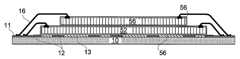
- FIG. 1shows an assembly including a die 22 mounted on a substrate 10 using a die attach epoxy.
- the die 22has a front side (“active” side) 23 adjacent which the integrated circuitry is formed, and a back side 21 , and sidewalls meeting the front and back sides at front and back edges.
- Die pads at the front side of the diearranged in this example as peripheral pads 24 , provide for electrical connection of the integrated circuitry of the die with underlying circuitry.
- the substrate 10 in this exampleincludes a patterned metal layer 12 on a dielectric layer.
- the patterned metal layer 12is covered by an electrically insulative layer 13 , which has openings exposing bond fingers 11 .
- the substratemay include one or more additional patterned metal layers, variously connected at vias through intervening dielectric layers, including a patterned metal layer at the surface opposite the die mount surface, at which lands are exposed to provide for connection to circuitry in a device in which the assembly is deployed.
- the die 22is in this example affixed to a die mount region of the substrate by a die attach epoxy 32 .
- the die mount procedureincludes dispensing a specified quantity of epoxy onto the insulative layer 13 , placing the die onto the epoxy, and curing the epoxy.
- a “fillet” 33is formed outside the die footprint at the periphery of the die mount region.
- the epoxy die attach processis carefully controlled to provide for a uniform die attach epoxy thickness and a limited spread of epoxy onto the substrate outside the die footprint.
- the dieis electrically connected to the circuitry on the substrate by wire bonds 14 connecting pads 24 with bond fingers 11 .
- a molding or encapsulationmay be formed over the assembly to protect the active side of the die and the interconnects.
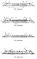
- FIG. 2shows an assembly including a first die 22 mounted on a substrate 10 generally as described with reference to FIG. 1 , and including an additional die 26 mounted on the first die 22 using a die attach epoxy.
- the additional die 26has a front side (“active” side) 27 adjacent which the integrated circuitry is formed, and a back side 25 , and sidewalls meeting the front and back sides at front and back edges.
- Die pads at the front side of the die, arranged in this example as peripheral pads 28provide for electrical connection of the integrated circuitry of the die with underlying circuitry.
- the second die 26is in this example affixed to a die mount region on the front side 23 of the first die 22 by a die attach epoxy 34 .
- the second die mount procedureincludes dispensing a specified quantity of epoxy onto a die attach region of the front side of die 22 , placing the second die onto the epoxy, and curing the epoxy.
- a “fillet” 35is formed outside the die footprint at the periphery of the die mount region.
- this second epoxy die attach processis carefully controlled to provide for a uniform die attach epoxy thickness and a limited spread of epoxy onto the first die surface 23 outside the die footprint.
- the dieis electrically connected to the circuitry on the substrate by wire bonds 16 connecting pads 28 with bond fingers 11 .
- a molding or encapsulationmay be formed over the assembly to protect the active side of the die and the interconnects.
- FIG. 3shows an assembly including a die 22 mounted on a substrate 10 using a film adhesive 42 .
- the die and the substrate, and their electrical connections to the substrate,are as in the example shown in FIG. 1 .
- the die 22is in this example affixed to a die mount region of the substrate by a film adhesive 42 .
- the die mount procedureincludes applying the film to either the backside of the die 22 or to the die mount region of the substrate 10 , thereafter placing the die onto the insulative layer 13 on the substrate, and thereafter (where the adhesive is curable) curing the adhesive.
- the adhesive filmis applied to the substrate, the film must first be cut to size, and then positioned on the substrate surface; where the film is applied to the die, this step may be performed at the wafer level, so that the film is cut to size during die singulation.
- the dieis electrically connected to the circuitry on the substrate by wire bonds 14 connecting pads 24 with bond fingers 11 .
- a molding or encapsulationmay be formed over the assembly to protect the active side of the die and the interconnects.
- FIG. 4shows an assembly including a first die 22 mounted on a substrate 10 generally as described with reference to FIG. 3 , and including an additional die 26 mounted on the first die 22 .
- the die and the substrate, and their electrical connections to the substrate,are as in the example shown in FIG. 3 .
- the second die mount procedureincludes applying the film to either the backside of the die 26 or to the die mount region of the front side of the first die 22 , thereafter placing the second die onto the first die, and thereafter (where the adhesive is curable) curing the adhesive.
- the filmmust first be cut to size, and then positioned on the surface of the first die; where the film is applied to the second die, this step may be performed at the wafer level, so that the film is cut to size during second die singulation.
- the second dieis electrically connected to the circuitry on the substrate by wire bonds 16 connecting pads 28 with bond fingers 11 .
- a molding or encapsulation(not shown in the FIG.) may be formed over the assembly to protect the active side of the die and the interconnects.
- a conformal coating on a semiconductor dieprovides adhesion between the die and a support. No additional adhesive is necessary to affix the die on the support.
- the conformal coatingprotects the die during assembly, and serves to electrically insulate the die from electrically conductive parts that the die may contact.
- the supportmay include a printed circuit board, or a substrate, or a leadframe, or another die, or an interposer, for example.
- the material of the conformal coatingincludes an organic polymer, for example a polymer of p-xylene or a derivative thereof, such as a polyxylylene polymer, e.g., a parylene C or a parylene N, or a parylene A, or a parylene SR.
- the conformal coatingis formed by deposition, for example by vapor deposition, or liquid phase deposition, or by solid phase deposition.
- the conformal coatingis formed on at least a die mount area of at least one side of the die, and the die is mounted on a die mount region of a support surface; adhesion of the die to the support is provided by the conformal coating on the die.
- the conformal coatingcovers the back side of the die, and may additionally cover one or more sidewalls, and may additionally cover the front side of the die; where the conformal coating covers the front side of the die, openings are provided in the coating to expose die pads for electrical connection of the die.
- the supportalso has a conformal coating, on at least the die mount region.
- the material of the conformal coating on the supportmay be the same as, or different from, the conformal coating on the die; in some embodiments the material of the conformal coating includes an organic polymer, for example a polymer of p-xylene or a derivative thereof, such as a polyxylylene polymer, e.g., a parylene C or a parylene N, or a parylene A, or a parylene SR.
- the conformal coatingis formed by deposition, for example by vapor deposition, or liquid phase deposition, or by solid phase deposition.
- the conformal coatingmay cover the front side of the die, and may additionally cover one or more sidewalls, and may additionally cover the back side of the die; where the conformal coating covers the front side of the die, openings are provided in the coating to expose die pads for electrical connection of the die.
- a method for affixing a die onto a supportincludes providing a die having a conformal coating, contacting a die attach area of the conformal coating with a die mount region of the support, and heating the die attach area of the conformal coating.
- the heating procedurefollows the contacting procedure; in some embodiments the contacting procedure follows the heating procedure. That is, the coated die may be heated prior to contacting the die and the support to make an assembly; or, the die and the support may be contacted to form an assembly, and the assembly may then be heated to effect adhesion.
- a method for affixing a die onto a supportincludes providing a die having a conformal coating, providing a support having a conformal coating, contacting a die attach area of the conformal coating on the die with a die mount region of the conformal coating on the support, and heating the die attach area of the conformal coating on the die or the die mount region of the conformal coating on the support.
- the heating procedurefollows the contacting procedure; in some embodiments the contacting procedure precedes the heating procedure. That is, the coated die may be heated prior to contacting the die and the support to make an assembly; or, the die and the support may be contacted to form an assembly, and the assembly may then be heated. In some embodiments the heating procedure follows the contacting procedure; in some embodiments the contacting procedure precedes the heating procedure.
- a method for affixing a die onto a supportincludes placing the die onto the support, providing a standoff between a die attach surface of the die and a die mount surface of the support, and carrying out a conformal coating process to coat at least the die attach surface and the die mount surface.
- the conformal coating materialmay be an organic polymer, such as a parylene, for example, and the conformal coating process may be a vapor deposition process; the polymer that forms in the space between the die surface and the support surface provides adhesion between the die and the support.
- the assemblies according to the disclosurecan be used for building computers, telecommunications equipment, and consumer and industrial electronics devices.
- FIG. 1is a diagrammatic sketch in a sectional view showing a die mounted onto a substrate using a conventional die mount epoxy.
- FIG. 2is a diagrammatic sketch in a sectional view showing a stack of two die mounted onto one another and mounted onto a substrate using a conventional die mount epoxy.
- FIG. 3is a diagrammatic sketch in a sectional view showing a die mounted onto a substrate using a conventional film adhesive.
- FIG. 4is a diagrammatic sketch in a sectional view showing a stack of two die mounted onto one another and mounted onto a substrate using a conventional film adhesive.
- FIG. 5is a diagrammatic sketch in a sectional view showing a die having a conformal coating over the front side, the back side, and sidewalls, the coating having openings exposing interconnect pads at the front side.
- FIG. 6is a diagrammatic sketch in a sectional view showing a die mounted onto a substrate according to an embodiment.
- FIG. 7is a diagrammatic sketch in a sectional view showing die mounted one upon the other in a die stack mounted onto a substrate according to an embodiment.
- FIG. 8is a diagrammatic sketch in a sectional view showing a die having a conformal coating over the front side, the back side, and sidewalls, the coating having openings exposing interconnect pads at the sidewalls.
- FIG. 9is a diagrammatic sketch in a sectional view showing a die having a conformal coating over the front side, the back side, and sidewalls, the coating having openings exposing interconnect pads at the sidewalls and at the front side adjacent front side edges.
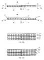
- FIGS. 10A , 11 Aare diagrammatic sketches in sectional view each showing a stack of four die mounted one onto another according to an embodiment.
- FIGS. 10B , 11 Bare diagrammatic sketches in sectional view each showing a four die stack as in FIGS. 10A , 11 A mounted onto and electrically interconnected with a substrate according to an embodiment.
- FIGS. 12A-12Care diagrammatic sketches in sectional view showing stages in construction of a conformally coated four die stack assembly according to an embodiment.
- U.S. Pat. No. 7,215,018describes a stacked die assembly including die each having a conformal coating on all six sides.
- the conformal coatingis said to provide electrical insulation and to reduce physical damage to the die during handling and processing.
- a polymer, for example parylene,is suggested as the die coating insulating material.
- the coated die in the stackare laminated on top of each other with an electrically insulating polymer or epoxy preformed sheet, which may include solid (for example, glass) spheres to maintain a fixed spacing and separation between the semiconductor die after lamination.
- FIG. 5there is shown in a diagrammatic sectional view a die 52 having a conformal coating 56 over the front side 53 , the back side 51 , and sidewalls 55 . Openings indicated by arrows 57 expose peripheral die pads 54 for electrical connection of the die.
- the material of the conformal coatingmay be an organic polymer, for example a polymer of p-xylene or a derivative thereof, such as a polyxylylene polymer, e.g., a parylene C or a parylene N, or a parylene A, or a parylene SR.
- a diemay be coated with a parylene as shown in FIG. 5 by a vapor phase polymerization process.
- Processes for forming paryleneare known.
- a para-xylylene dimeris vaporized at a pressure below atmosphere and at a temperature sufficient to vaporize the dimer at that pressure; then the vaporized dimer is pyrolized by heating to form the reactive para-xylylene monomer; then the reactive monomer and the item to be coated are brought together in a chamber with ambient temperature and reduced pressure, whereupon the reactive monomer condenses on all exposed surfaces within the chamber, including all exposed surface of the item, and polymerizes in situ.
- various process parameterscan be controlled to determine the thickness of the resulting coating.
- the thicknessshould be at least sufficient to provide insulation; and where the parylene coating on a die surface provides a barrier, for example to moisture, the thickness should be at least sufficient to provide such a barrier.
- the parylene coating on a die surface to be mated to another die surfacehas a thickness in a range about 0.1 micron to about 100 microns, more usually in a range in the order of one to a few microns to a few tens of microns.
- the diemay be positioned in the chamber such that one or more of the six sides of the die are entirely or partially obscured.
- the coatingmay be carried out, for example, at the wafer level, and as a result only the exposed surface of the wafer will be coated; subsequent die singulation results in die coated only on the corresponding surface of the die.
- the coatingmay be carried out at a die array level, in which the wafer is partly or fully sawn; the resulting coating will cover part or the entirety of the sidewalls and either the die back sides (if the back side of the wafer is exposed) or the front sides (if the front side of the wafer is exposed) of the resulting die will be covered.
- coating of all sides of the diemay be obtained by carrying out two coating procedures, and turning the die (or wafer) over between the two procedures. Examples of various procedures for coating die at the wafer level and the die array level are described in, for example, S. J. S. McElrea et al. U.S. application Ser. No. 12/142,589, titled “Wafer level surface passivation of stackable integrated circuit chips”, which was filed on Jun. 19, 2008, and which is incorporated by reference herein.
- openings in the coatingmay be formed, for example, by laser ablation.
- FIG. 6shows an assembly including a conformally coated die mounted onto a substrate according to an embodiment of the invention.
- the substrate 10is configured in this example substantially as in FIGS. 1-4
- the die 52is configured substantially as in FIG. 5 .
- the coated die in this examplerests directly on the substrate (that is, directly on the dielectric layer 13 overlying the patterned metal layer 12 ), and adhesion of the coated die to the die attach region of the substrate is provided by the coating 56 at the die attach area on the back side of the die.
- Adhesion of the coated die to the substrateis accomplished by heating the coating at the die attach area on the back side of the die to a temperature sufficient to affect adhesion of the die attach area with the substrate. This may be accomplished by, for example, heating the coated die to a temperature at which the material of the coating has some degree of surface tack, and then placing the die onto the die attach region of the substrate with the tacky surface contacting the substrate surface (that is, contacting the dielectric layer 13 overlying the patterned metal layer 12 ). Or, the coated die may be placed upon the substrate to make a die-on-substrate assembly, and then the assembly may be heated to heat the coating. As may be appreciated, the placing and the heating may be carried out sequentially or to some extent concurrently.
- the coatingmay be heated by convection or by conduction, for example, employing radiation (such as microwave radiation) or employing a heated platform, for example; and in some embodiments the substrate may be heated so that the coating is heated upon contact with the heated substrate.
- adhesionmay be accomplished by heating to a temperature in a range about 120° C. to about 230° C., usually not greater than about 175° C. to about 200° C. and more usually in a range about 125° C. to about 150° C. (excessive heating may damage the parylene coating).
- Adhesionmay optionally be facilitated by application of pressure between the die and the substrate in addition to heat, and in some examples, where a parylene is used, applying a pressure about 5 N per square cm, or weighting the die on the substrate with a mass equivalent to about 10 kg per square cm, may be useful. Uniform adhesion may be facilitated by heating (and optionally applying pressure) for a time in a range about 1 second to about 30 minutes, for example about 10 minutes.
- the die 52is electrically connected to circuitry in the substrate 10 , in this example by wire bonds connecting exposed die pads 54 to bond fingers 11 . Openings are made in the coating at selected sites, for example by laser ablation, to expose the die pads prior to wire bond formation; opening may be carried out at any stage after the front side is coated and before the wire bond is attached, as may be convenient for the particular process.
- FIG. 7shows an assembly including a first coated die 52 mounted on a substrate 10 generally as described with reference to FIG. 6 , and including an additional coated die 56 mounted on the first die 52 .
- the additional die 56has a front side (“active” side) adjacent which the integrated circuitry is formed, and a back side, and sidewalls meeting the front and back sides at front and back edges. Die pads at the front side of the die, arranged in this example as peripheral pads, provide for electrical connection of the integrated circuitry of the additional die with underlying circuitry.
- the additional dieis affixed to a die mount region on the front side of the first die 52 by adhesion between the coatings on the opposed surfaces of the respective die, that is, on the front side of the first die and on the back side of the additional die.
- the second die mount proceduremay be carried out substantially as for the first die mount. That is, the coated second die may be heated and then placed upon the first die (and, optionally, pressure may be applied between the second die and the first die), or the second die may be placed on the first die and then the assembly may be heated (and, optionally, pressure may be applied). Or, alternatively, all the die may be placed one over another on the substrate to form a stacked die-on-substrate assembly, and then the assembly may be heated (and, optionally, pressure may be applied) to effect adhesion.
- the additional dieis electrically connected to the circuitry on the substrate by wire bonds 16 connecting die pads on the additional die with bond fingers 11 . Openings are made in the coating at selected sites, to expose die pads prior to wire bond formation.
- a molding or encapsulation(not shown in this FIG.) may be formed over the assembly to protect the active side of the die and the interconnects.
- a die stack, not affixed to a non-die supportmay optionally be made by providing a first coated die and a second coated die, and heating a contact area of the coating on at least one of the die, and then placing one die onto the die attach region of the other die with a contact area of the surface of one coating contacting the die attach region of the surface of the other coating (and, optionally, applying pressure). This can be completed for any number of additional die, to form a multiple die stack of adhered die. Or, the die may be positioned one upon another to form a stack, and then the stack can be heated (and, optionally, pressure applied) to effect adhesion of all the die at once to form a multiple die stack of adhered die.
- one or more stacks of diemay be held in a fixture, adapted to maintain the relative positions of the die in the stack, and optionally adapted to provide a compressive force on the stack.
- suitable fixturesare described, for example, in McGrath et al. International Application No. PCT/US08/6651, titled “Method for optimized integrated circuit chip interconnection”, and in McGrath et al. International Application No. PCT/US08/66568, tiled “Semiconductor die coating and interconnection fixture and method”, each of which was filed Jun. 11, 2008.
- the completed stack of adhered diecan then be mounted on a non-die support either by adhesion of the coating on the die that contacts the non-die support (such as, for example, a printed circuit board, or a package substrate, or a leadframe), or by a conventional adhesive.
- a non-die supportsuch as, for example, a printed circuit board, or a package substrate, or a leadframe
- FIGS. 6 and 7employ electrical connection by wire bonds.
- Other interconnectsmay be employed, and may be preferred.
- a trace of electrically conductive polymerfor example electrically conductive epoxy or electrically conductive ink, may be laid down to connect a die pad with a bond site in electrical circuitry on a support. Where the conformal coating covers at least those areas of the die that are directly overlain by the epoxy trace, electrical shorting of the epoxy interconnect is avoided.
- a conductive epoxy tracemay begin with electrical contact at an exposed die pad on the second die 56 , may be drawn across the coated (thereby electrically insulated) margin and front edge of the second die 56 , down over the sidewall to the coated (and thereby electrically insulated) front side of the first die 52 , may optionally make electrical contact with an exposed die pad on the first die 52 , may be drawn across the coated (thereby electrically insulated) margin and front edge of the first die 52 , down over the sidewall to the surface of the substrate 10 , which is insulated by the dielectric layer 13 , and may end with electrical contact with an exposed bond finger 11 .
- FIGS. 8 and 9show, in diagrammatic sectional view, embodiments of conformally coated die having interconnect terminals exposed at the sidewalls of the die.
- a die 82has a front side 83 and a back side 81 and sidewalls 85 , all coated with a conformal coating 86 , except that interconnect terminals 84 are situated at the sidewalls and exposed as indicted by arrows 87 .
- interconnect terminals 84are situated at the sidewalls and exposed as indicted by arrows 87 .
- a die 92has a front side 93 and a back side 91 and sidewalls 95 , all coated with a conformal coating 96 , except that interconnect terminals 94 wrap around a front edge of the die (which may optionally be chamfered) and are exposed at the sidewall and at the margin of the front side, and at the die edge as indicated by arrows 97 .
- Coated die as in FIGS. 8 and 9may optionally be stacked with sidewalls aligned, as shown in FIGS. 10A and 11A , respectively, and affixed by adhesion of the coatings as described above.
- the interconnect terminals 87 , 87 ′, 87 ′′, 87 ′′′ (in FIG. 10A ) and the interconnect terminals 97 , 97 ′, 97 ′′, 97 ′′′ (in FIG. 11A ),are now aligned, “vertically” with respect to an arbitrarily assigned “horizontal” plane of the front or back sides of the die and, accordingly, they may be vertically interconnected, for example using a trace of electrically conductive epoxy.
- FIGS. 10B and 11Brespectively show stacked die as in FIGS. 10A and 11A with the die in each stack electrically interconnected and each stack connected to a substrate. Referring to FIG.
- a substrate 100is shown having a patterned metal layer 102 on a dielectric layer, and covered by an insulative layer 103 except where, as indicated at 109 , vertical interconnection is to be made.
- a stack of die as in FIG. 10Ais mounted onto the substrate 100 , affixed by adhesion of the conformal coating on the backside of the die 82 to a die mount region of the substrate surface.
- Vertical interconnectionis made by conductive epoxy traces 107 , which make electrical contact with interconnect terminals 87 at the sidewalls of the die and with the exposed interconnect sites 109 . Referring to FIG.
- a substrate 110is shown having a patterned metal layer 112 on a dielectric layer, and covered by an insulative layer 113 except where, as indicated at 119 , vertical interconnection is to be made.
- a stack of die as in FIG. 11Ais mounted onto the substrate 110 , affixed by adhesion of the conformal coating on the backside of the die 92 to a die mount region of the substrate surface.
- Vertical interconnectionis made by conductive epoxy traces 117 , which make electrical contact with interconnect terminals 97 at the sidewalls of the die and with the exposed interconnect sites 119 .
- individual dieare provided prior to stacking and adhesion with a conformal coating over at least a contact area; and the coated die are stacked and treated to effect adhesion.
- the dieare coated on the front side, the back side, and the sidewalls; but it is not necessary that all the surfaces of the die be coated.
- the conformal coatingmay be applied to only one of the mutually opposed die attach surfaces, to effect adhesion of the die with a non-die support or with another die.
- Further surfaces (or areas of surfaces) of the diemay be coated, for example to provide electrical insulation, so that shorting is avoided between the die surface and overarching or overlying electrical interconnects (bond wires or conductive epoxy traces, for example).
- uncoated diemay be stacked and then a coating process may be applied to the stack.
- a paryleneis formed using a dry vapor deposition
- the active monomercondenses on surfaces within very small (narrow) spaces and, accordingly, the polymer can form in a very thin space between adjacent die.
- Such a very thin layer of polymercan suffice to effect adhesion between adjacent die. Stages in an example of such a process are shown by way of example in FIGS. 12A , 12 B, 12 C.
- the height of the spacers as provided on the surfaceis selected to provide the desired gap; the number of small spacers and their arrangement on the surface can be selected to provide support and the desired spacing.
- the film or supportis substantially incompressible under the processing conditions, or compressible to a determinable extent.
- the film or spacersmay optionally be adhesive, and may optionally be a curable adhesive, so that the film or spacers can provide temporary adhesion between the surfaces, to maintain the relative positions of the parts. This temporary adhesion (where employed) is typically insufficient to securely affix the die to the support, and permanent adhesion is provided by a parylene filling the gap, as described below.
- the nonconducting filmmay be an epoxy preform, for example; and the spacers may be small spots or puddles of an epoxy, for example, dispensed or printed in a suitable pattern.
- the small supportsmay be (or include) spacer elements of an electrically nonconductive material (such as a glass or an organic polymer) that are dimensioned to provide the desired spacing, and, optionally, they may be provided with a thin surface adhesive to provide temporary adhesion.
- the spacer elementsmay have any of a variety of shapes; if spherical, for example, their diameter can provide the appropriate spacing and if spheroidal, for example, their smaller diameter can provide the appropriate spacing.
- the die as provided by the manufacturerhas a protective passivation layer covering at least the active surface.
- This protective layermay be an organic polymer such as a polyimide, for example, and typically may have a thickness in a range about 5 um to about 6 um. Where a gap between surfaces in a range about the same as the passivation layer is desired, a significant portion of the passivation layer may be selectively removed (for example, in a patterned selective etch process) leaving small spots or areas of the passivation layer (for example, at the corners of the die; or at the corners and abut the center of the die) to serve as spacers.
- FIG. 12Ashows four die 112 , 112 ′, 112 ′′, 112 ′′′, selected 120 for assembly into a four-die stack.
- Each die except the topmost one in the stackis provided with (in this example) a number of generally spheroidal spacer elements 114 all having approximately the same nominal height.
- the material of the spacer elementsis electrically nonconductive.
- the spacer elementsprovide a standoff, or gap or space 113 , between adjacent die, and the height of the spacer elements determines the thickness of the standoff.
- the spacer elementsmay have a nominal height in a range about 5 um to about 40 um, for example; in some embodiments the gap between adjacent die may be about 10 um, or about 20 um. As will be appreciated, for a given number of die in the stack thinner gaps between adjacent die results, desirably in some applications, in a thinner overall stack and in some embodiments the gap may be made less than 5 um.
- the assembly of spaced-apart dieis then subjected to a conformal coating process, resulting in a coated stacked die assembly 124 , as shown in FIG. 12C .
- the coating 116forms on all exposed surfaces of the assembly, including a die active side at the “top” of the stack, a die backside at the “bottom” of the stack, and die sidewalls; and including the spaced-apart front sides and back sides of adjacent die in the stack, as indicated at 117 .
- the parylene coatingis formed by a dry vapor deposition.
- the active monomercondenses on surfaces within very small (narrow) spaces and, accordingly, the polymer can form in a very thin space between adjacent die.
- the thinness of a gap between surfaces that can be successfully filled by a parylenedepends upon the distance from the edge to the center of the surfaces in the gap, and upon the mean free path of the parylene under the processing conditions employed.
- the capacity of the parylene monomer to invade the gapcan limit the extent of thinness of the gap.
- the various paryleneshave different characteristics, including mean free path characteristics, and for gap filling the choice of parylene and selection of processing conditions can be readily determined accordingly.
- the gap surfaces to be coatedcan, for example, be differentially cooled, to promote coating formation from within the gap toward the outside to fill the gap.
- the individual dieare provided prior to stacking and adhesion with a conformal coating over at least a contact area; the coated die are stacked to form an assembly of coated die; and the assembly of coated die is subjected to a further conformal coating process to encapsulate the stack and, optionally, to effect adhesion of the die in the stack and/or the stack to an additional stack or to a non-die support.
- spacer elementsmay be required to provide adequate support, depending for example upon the flexibility of the die (thinner die may require more support) and upon the height of the stack and the number of die in the stack.
- the spacer elementsmay be, for example, glass or nonconductive polymer spheres; and they may be scattered over the surface of each die.
- the spacersmay be small polymer dots, which may be adhesive to some extent (they may be a polymer adhesive, for example an epoxy) to affix the adjacent die temporarily, so that the die in the stack do not shift during processing steps leading up to the completion of the conformal coating over the stack; and they may be printed (for example screen printed or mask printed) onto the die surface, or dispensed onto the die surface using a needle or nozzle, for example.
- the coatingneed be situated only within an area where contact of the surface of the coated die and the surface of the substrate is expected. For example, where the backside of the coated die contacts a surface of the substrate, for adhesion purposes the coating may be only within the die attach area of the die.
- the supportmay include a patterned metal layer at the die mount side, as shown by way of example in FIGS. 6 , 7 , 10 B and 11 B.
- the dielectric layer over the patterned metal layere.g. 13 , 103 , 113 ) is not required, as the dielectric properties of the conformal coating prevents shorting of the die and the circuitry on the substrate.
- the dieare shown as having the same width (in the sectional view shown), and the die are arranged in the stack so that the die sidewalls in overlying die are generally vertically aligned. That is, the resulting die stack assemblies present a generally planar stack face for interconnection. In other embodiments, not all the die in the stack need have the same dimensions, and the die sidewalls adjacent the interconnects may be arranged so that they are not vertically aligned. For example, the die in the stack may be offset, or may be staggered. Examples of various die stacking configurations are shown in S. J. S. McElrea et al. U.S. application Ser. No. 12/124,077, referenced above.
- the diemay be interconnected by tab bonds, for example, or by ribbon bonds configured as off-die interconnects.
- vertical interconnectionis employed, for example using an electrically conductive epoxy trace
- adjacent die in the stackmay be offset.
- An offset arrangementmay be particularly useful where the die pads or interconnects are situated in the active surface of the die and are accordingly would not be presented at the face of the die stack for interconnection.
- a stack of several offset diemay have a stairstep appearance, for example. All patents and patent applications referred to above are hereby incorporated by reference herein.
Landscapes
- Engineering & Computer Science (AREA)
- Microelectronics & Electronic Packaging (AREA)
- Power Engineering (AREA)
- Computer Hardware Design (AREA)
- Physics & Mathematics (AREA)
- Condensed Matter Physics & Semiconductors (AREA)
- General Physics & Mathematics (AREA)
- Manufacturing & Machinery (AREA)
- Structures Or Materials For Encapsulating Or Coating Semiconductor Devices Or Solid State Devices (AREA)
- Die Bonding (AREA)
- Encapsulation Of And Coatings For Semiconductor Or Solid State Devices (AREA)
Abstract
Description
- This application claims priority from S. J. Crane et al. U.S. Provisional Application No. 60/971,203, titled “Semiconductor die mount by conformal die coating”, which was filed on Sep. 10, 2007, and which is incorporated by reference herein.
- This application is related to S. J. S McElrea et al. U.S. application Ser. No. 12/124,077, titled “Electrically interconnected stacked die assemblies”, which was filed on May 20, 2008, and which is incorporated by reference herein.
- This invention relates to mounting semiconductor die on a support.
- A semiconductor integrated circuit die may be mounted directly onto a printed circuit board; or on a leadframe or a substrate; or on another semiconductor die in a stacked die assembly.
- A semiconductor integrated circuit die is conventionally mounted on the support using an adhesive. Die mount adhesives may take the form of a die attach epoxy, as illustrated for example in
FIGS. 1 and 2 ; or an adhesive film, as illustrated for example inFIGS. 3 and 4 . FIG. 1 shows an assembly including a die22 mounted on asubstrate 10 using a die attach epoxy. The die22 has a front side (“active” side)23 adjacent which the integrated circuitry is formed, and aback side 21, and sidewalls meeting the front and back sides at front and back edges. Die pads at the front side of the die, arranged in this example asperipheral pads 24, provide for electrical connection of the integrated circuitry of the die with underlying circuitry.- The
substrate 10 in this example includes apatterned metal layer 12 on a dielectric layer. The patternedmetal layer 12 is covered by an electricallyinsulative layer 13, which has openings exposingbond fingers 11. The substrate may include one or more additional patterned metal layers, variously connected at vias through intervening dielectric layers, including a patterned metal layer at the surface opposite the die mount surface, at which lands are exposed to provide for connection to circuitry in a device in which the assembly is deployed. - The die22 is in this example affixed to a die mount region of the substrate by a die
attach epoxy 32. The die mount procedure includes dispensing a specified quantity of epoxy onto theinsulative layer 13, placing the die onto the epoxy, and curing the epoxy. Typically a “fillet”33 is formed outside the die footprint at the periphery of the die mount region. The epoxy die attach process is carefully controlled to provide for a uniform die attach epoxy thickness and a limited spread of epoxy onto the substrate outside the die footprint. Following die attach, the die is electrically connected to the circuitry on the substrate bywire bonds 14 connectingpads 24 withbond fingers 11. A molding or encapsulation (not shown in the FIG.) may be formed over the assembly to protect the active side of the die and the interconnects. FIG. 2 shows an assembly including afirst die 22 mounted on asubstrate 10 generally as described with reference toFIG. 1 , and including anadditional die 26 mounted on thefirst die 22 using a die attach epoxy. The additional die26 has a front side (“active” side)27 adjacent which the integrated circuitry is formed, and aback side 25, and sidewalls meeting the front and back sides at front and back edges. Die pads at the front side of the die, arranged in this example asperipheral pads 28, provide for electrical connection of the integrated circuitry of the die with underlying circuitry.- The second die26 is in this example affixed to a die mount region on the
front side 23 of the first die22 by a dieattach epoxy 34. The second die mount procedure, as with the first die mount procedure, includes dispensing a specified quantity of epoxy onto a die attach region of the front side of die22, placing the second die onto the epoxy, and curing the epoxy. Typically a “fillet”35 is formed outside the die footprint at the periphery of the die mount region. As in the first die attach process, this second epoxy die attach process is carefully controlled to provide for a uniform die attach epoxy thickness and a limited spread of epoxy onto thefirst die surface 23 outside the die footprint. Following die attach, the die is electrically connected to the circuitry on the substrate bywire bonds 16 connectingpads 28 withbond fingers 11. A molding or encapsulation (not shown in the FIG.) may be formed over the assembly to protect the active side of the die and the interconnects. FIG. 3 shows an assembly including adie 22 mounted on asubstrate 10 using afilm adhesive 42. The die and the substrate, and their electrical connections to the substrate, are as in the example shown inFIG. 1 .- The die22 is in this example affixed to a die mount region of the substrate by a film adhesive42. The die mount procedure includes applying the film to either the backside of the
die 22 or to the die mount region of thesubstrate 10, thereafter placing the die onto theinsulative layer 13 on the substrate, and thereafter (where the adhesive is curable) curing the adhesive. Where the adhesive film is applied to the substrate, the film must first be cut to size, and then positioned on the substrate surface; where the film is applied to the die, this step may be performed at the wafer level, so that the film is cut to size during die singulation. Following die attach, the die is electrically connected to the circuitry on the substrate bywire bonds 14 connectingpads 24 withbond fingers 11. A molding or encapsulation (not shown in the FIG.) may be formed over the assembly to protect the active side of the die and the interconnects. FIG. 4 shows an assembly including afirst die 22 mounted on asubstrate 10 generally as described with reference toFIG. 3 , and including anadditional die 26 mounted on thefirst die 22. The die and the substrate, and their electrical connections to the substrate, are as in the example shown inFIG. 3 . The second die mount procedure, as with the first die mount procedure, includes applying the film to either the backside of thedie 26 or to the die mount region of the front side of thefirst die 22, thereafter placing the second die onto the first die, and thereafter (where the adhesive is curable) curing the adhesive. Where the adhesive film is applied to the substrate, the film must first be cut to size, and then positioned on the surface of the first die; where the film is applied to the second die, this step may be performed at the wafer level, so that the film is cut to size during second die singulation. Following die attach, the second die is electrically connected to the circuitry on the substrate bywire bonds 16 connectingpads 28 withbond fingers 11. A molding or encapsulation (not shown in the FIG.) may be formed over the assembly to protect the active side of the die and the interconnects.- In a general aspect of the disclosure, a conformal coating on a semiconductor die provides adhesion between the die and a support. No additional adhesive is necessary to affix the die on the support. The conformal coating protects the die during assembly, and serves to electrically insulate the die from electrically conductive parts that the die may contact.
- In various embodiments the support may include a printed circuit board, or a substrate, or a leadframe, or another die, or an interposer, for example.
- In some embodiments the material of the conformal coating includes an organic polymer, for example a polymer of p-xylene or a derivative thereof, such as a polyxylylene polymer, e.g., a parylene C or a parylene N, or a parylene A, or a parylene SR. In some embodiments the conformal coating is formed by deposition, for example by vapor deposition, or liquid phase deposition, or by solid phase deposition.
- The conformal coating is formed on at least a die mount area of at least one side of the die, and the die is mounted on a die mount region of a support surface; adhesion of the die to the support is provided by the conformal coating on the die.
- In some embodiments the conformal coating covers the back side of the die, and may additionally cover one or more sidewalls, and may additionally cover the front side of the die; where the conformal coating covers the front side of the die, openings are provided in the coating to expose die pads for electrical connection of the die.
- In some embodiments the support also has a conformal coating, on at least the die mount region. The material of the conformal coating on the support may be the same as, or different from, the conformal coating on the die; in some embodiments the material of the conformal coating includes an organic polymer, for example a polymer of p-xylene or a derivative thereof, such as a polyxylylene polymer, e.g., a parylene C or a parylene N, or a parylene A, or a parylene SR. In some embodiments the conformal coating is formed by deposition, for example by vapor deposition, or liquid phase deposition, or by solid phase deposition.
- Where the support is another die, the conformal coating may cover the front side of the die, and may additionally cover one or more sidewalls, and may additionally cover the back side of the die; where the conformal coating covers the front side of the die, openings are provided in the coating to expose die pads for electrical connection of the die.
- In another general aspect of the disclosure, a method for affixing a die onto a support includes providing a die having a conformal coating, contacting a die attach area of the conformal coating with a die mount region of the support, and heating the die attach area of the conformal coating. In some embodiments the heating procedure follows the contacting procedure; in some embodiments the contacting procedure follows the heating procedure. That is, the coated die may be heated prior to contacting the die and the support to make an assembly; or, the die and the support may be contacted to form an assembly, and the assembly may then be heated to effect adhesion.
- In another general aspect of the disclosure, a method for affixing a die onto a support includes providing a die having a conformal coating, providing a support having a conformal coating, contacting a die attach area of the conformal coating on the die with a die mount region of the conformal coating on the support, and heating the die attach area of the conformal coating on the die or the die mount region of the conformal coating on the support.
- In some embodiments the heating procedure follows the contacting procedure; in some embodiments the contacting procedure precedes the heating procedure. That is, the coated die may be heated prior to contacting the die and the support to make an assembly; or, the die and the support may be contacted to form an assembly, and the assembly may then be heated. In some embodiments the heating procedure follows the contacting procedure; in some embodiments the contacting procedure precedes the heating procedure.
- In another general aspect of the disclosure, a method for affixing a die onto a support includes placing the die onto the support, providing a standoff between a die attach surface of the die and a die mount surface of the support, and carrying out a conformal coating process to coat at least the die attach surface and the die mount surface. The conformal coating material may be an organic polymer, such as a parylene, for example, and the conformal coating process may be a vapor deposition process; the polymer that forms in the space between the die surface and the support surface provides adhesion between the die and the support.
- The assemblies according to the disclosure can be used for building computers, telecommunications equipment, and consumer and industrial electronics devices.
FIG. 1 is a diagrammatic sketch in a sectional view showing a die mounted onto a substrate using a conventional die mount epoxy.FIG. 2 is a diagrammatic sketch in a sectional view showing a stack of two die mounted onto one another and mounted onto a substrate using a conventional die mount epoxy.FIG. 3 is a diagrammatic sketch in a sectional view showing a die mounted onto a substrate using a conventional film adhesive.FIG. 4 is a diagrammatic sketch in a sectional view showing a stack of two die mounted onto one another and mounted onto a substrate using a conventional film adhesive.FIG. 5 is a diagrammatic sketch in a sectional view showing a die having a conformal coating over the front side, the back side, and sidewalls, the coating having openings exposing interconnect pads at the front side.FIG. 6 is a diagrammatic sketch in a sectional view showing a die mounted onto a substrate according to an embodiment.FIG. 7 is a diagrammatic sketch in a sectional view showing die mounted one upon the other in a die stack mounted onto a substrate according to an embodiment.FIG. 8 is a diagrammatic sketch in a sectional view showing a die having a conformal coating over the front side, the back side, and sidewalls, the coating having openings exposing interconnect pads at the sidewalls.FIG. 9 is a diagrammatic sketch in a sectional view showing a die having a conformal coating over the front side, the back side, and sidewalls, the coating having openings exposing interconnect pads at the sidewalls and at the front side adjacent front side edges.FIGS. 10A ,11A are diagrammatic sketches in sectional view each showing a stack of four die mounted one onto another according to an embodiment.FIGS. 10B ,11B are diagrammatic sketches in sectional view each showing a four die stack as inFIGS. 10A ,11A mounted onto and electrically interconnected with a substrate according to an embodiment.FIGS. 12A-12C are diagrammatic sketches in sectional view showing stages in construction of a conformally coated four die stack assembly according to an embodiment.- The invention will now be described in further detail by reference to the drawings, which illustrate alternative embodiments. The drawings are diagrammatic, showing features of the invention and their relation to other features and structures, and are not made to scale. For improved clarity of presentation, in the FIGs. illustrating various embodiments, elements corresponding to elements shown in other drawings are not all particularly renumbered, although they are all readily identifiable in all the FIGs. Also for clarity of presentation certain features are not shown in the FIGs., where not necessary for an understanding of the disclosure.
- U.S. Pat. No. 7,215,018 describes a stacked die assembly including die each having a conformal coating on all six sides. The conformal coating is said to provide electrical insulation and to reduce physical damage to the die during handling and processing. A polymer, for example parylene, is suggested as the die coating insulating material. The coated die in the stack are laminated on top of each other with an electrically insulating polymer or epoxy preformed sheet, which may include solid (for example, glass) spheres to maintain a fixed spacing and separation between the semiconductor die after lamination.
- Turning now to
FIG. 5 , there is shown in a diagrammatic sectional view adie 52 having aconformal coating 56 over thefront side 53, theback side 51, and sidewalls55. Openings indicated byarrows 57 exposeperipheral die pads 54 for electrical connection of the die. The material of the conformal coating may be an organic polymer, for example a polymer of p-xylene or a derivative thereof, such as a polyxylylene polymer, e.g., a parylene C or a parylene N, or a parylene A, or a parylene SR. - A die may be coated with a parylene as shown in
FIG. 5 by a vapor phase polymerization process. Processes for forming parylene are known. In one process, a para-xylylene dimer is vaporized at a pressure below atmosphere and at a temperature sufficient to vaporize the dimer at that pressure; then the vaporized dimer is pyrolized by heating to form the reactive para-xylylene monomer; then the reactive monomer and the item to be coated are brought together in a chamber with ambient temperature and reduced pressure, whereupon the reactive monomer condenses on all exposed surfaces within the chamber, including all exposed surface of the item, and polymerizes in situ. As is well known various process parameters can be controlled to determine the thickness of the resulting coating. Where the parylene coating on the die surface provides electrical insulation between adjacent parts, the thickness should be at least sufficient to provide insulation; and where the parylene coating on a die surface provides a barrier, for example to moisture, the thickness should be at least sufficient to provide such a barrier. In some examples the parylene coating on a die surface to be mated to another die surface has a thickness in a range about 0.1 micron to about 100 microns, more usually in a range in the order of one to a few microns to a few tens of microns. - Various of these procedures may be carried out sequentially or at least partly concurrently, and they may be carried out in a staged processing apparatus. The die may be positioned in the chamber such that one or more of the six sides of the die are entirely or partially obscured. The coating may be carried out, for example, at the wafer level, and as a result only the exposed surface of the wafer will be coated; subsequent die singulation results in die coated only on the corresponding surface of the die. Or, the coating may be carried out at a die array level, in which the wafer is partly or fully sawn; the resulting coating will cover part or the entirety of the sidewalls and either the die back sides (if the back side of the wafer is exposed) or the front sides (if the front side of the wafer is exposed) of the resulting die will be covered. Or, coating of all sides of the die may be obtained by carrying out two coating procedures, and turning the die (or wafer) over between the two procedures. Examples of various procedures for coating die at the wafer level and the die array level are described in, for example, S. J. S. McElrea et al. U.S. application Ser. No. 12/142,589, titled “Wafer level surface passivation of stackable integrated circuit chips”, which was filed on Jun. 19, 2008, and which is incorporated by reference herein.
- Where as a result of the vapor phase polymerization process the front side of the die is covered, openings in the coating may be formed, for example, by laser ablation.
FIG. 6 shows an assembly including a conformally coated die mounted onto a substrate according to an embodiment of the invention. Thesubstrate 10 is configured in this example substantially as inFIGS. 1-4 , and thedie 52 is configured substantially as inFIG. 5 . The coated die in this example rests directly on the substrate (that is, directly on thedielectric layer 13 overlying the patterned metal layer12), and adhesion of the coated die to the die attach region of the substrate is provided by thecoating 56 at the die attach area on the back side of the die.- Adhesion of the coated die to the substrate is accomplished by heating the coating at the die attach area on the back side of the die to a temperature sufficient to affect adhesion of the die attach area with the substrate. This may be accomplished by, for example, heating the coated die to a temperature at which the material of the coating has some degree of surface tack, and then placing the die onto the die attach region of the substrate with the tacky surface contacting the substrate surface (that is, contacting the
dielectric layer 13 overlying the patterned metal layer12). Or, the coated die may be placed upon the substrate to make a die-on-substrate assembly, and then the assembly may be heated to heat the coating. As may be appreciated, the placing and the heating may be carried out sequentially or to some extent concurrently. The coating may be heated by convection or by conduction, for example, employing radiation (such as microwave radiation) or employing a heated platform, for example; and in some embodiments the substrate may be heated so that the coating is heated upon contact with the heated substrate. For example, where a parylene is used, adhesion may be accomplished by heating to a temperature in a range about 120° C. to about 230° C., usually not greater than about 175° C. to about 200° C. and more usually in a range about 125° C. to about 150° C. (excessive heating may damage the parylene coating). Adhesion may optionally be facilitated by application of pressure between the die and the substrate in addition to heat, and in some examples, where a parylene is used, applying a pressure about 5 N per square cm, or weighting the die on the substrate with a mass equivalent to about 10 kg per square cm, may be useful. Uniform adhesion may be facilitated by heating (and optionally applying pressure) for a time in a range about 1 second to about 30 minutes, for example about 10 minutes. - Following die attach, the
die 52 is electrically connected to circuitry in thesubstrate 10, in this example by wire bonds connecting exposeddie pads 54 tobond fingers 11. Openings are made in the coating at selected sites, for example by laser ablation, to expose the die pads prior to wire bond formation; opening may be carried out at any stage after the front side is coated and before the wire bond is attached, as may be convenient for the particular process. FIG. 7 shows an assembly including a first coated die52 mounted on asubstrate 10 generally as described with reference toFIG. 6 , and including an additional coated die56 mounted on thefirst die 52. The additional die56 has a front side (“active” side) adjacent which the integrated circuitry is formed, and a back side, and sidewalls meeting the front and back sides at front and back edges. Die pads at the front side of the die, arranged in this example as peripheral pads, provide for electrical connection of the integrated circuitry of the additional die with underlying circuitry. The additional die is affixed to a die mount region on the front side of thefirst die 52 by adhesion between the coatings on the opposed surfaces of the respective die, that is, on the front side of the first die and on the back side of the additional die.- The second die mount procedure, as with the first die mount procedure, may be carried out substantially as for the first die mount. That is, the coated second die may be heated and then placed upon the first die (and, optionally, pressure may be applied between the second die and the first die), or the second die may be placed on the first die and then the assembly may be heated (and, optionally, pressure may be applied). Or, alternatively, all the die may be placed one over another on the substrate to form a stacked die-on-substrate assembly, and then the assembly may be heated (and, optionally, pressure may be applied) to effect adhesion. Following die attach, the additional die is electrically connected to the circuitry on the substrate by
wire bonds 16 connecting die pads on the additional die withbond fingers 11. Openings are made in the coating at selected sites, to expose die pads prior to wire bond formation. A molding or encapsulation (not shown in this FIG.) may be formed over the assembly to protect the active side of the die and the interconnects. - A die stack, not affixed to a non-die support, may optionally be made by providing a first coated die and a second coated die, and heating a contact area of the coating on at least one of the die, and then placing one die onto the die attach region of the other die with a contact area of the surface of one coating contacting the die attach region of the surface of the other coating (and, optionally, applying pressure). This can be completed for any number of additional die, to form a multiple die stack of adhered die. Or, the die may be positioned one upon another to form a stack, and then the stack can be heated (and, optionally, pressure applied) to effect adhesion of all the die at once to form a multiple die stack of adhered die. Optionally one or more stacks of die may be held in a fixture, adapted to maintain the relative positions of the die in the stack, and optionally adapted to provide a compressive force on the stack. Examples of suitable fixtures are described, for example, in McGrath et al. International Application No. PCT/US08/6651, titled “Method for optimized integrated circuit chip interconnection”, and in McGrath et al. International Application No. PCT/US08/66568, tiled “Semiconductor die coating and interconnection fixture and method”, each of which was filed Jun. 11, 2008. The completed stack of adhered die can then be mounted on a non-die support either by adhesion of the coating on the die that contacts the non-die support (such as, for example, a printed circuit board, or a package substrate, or a leadframe), or by a conventional adhesive.
- The examples shown in
FIGS. 6 and 7 employ electrical connection by wire bonds. Other interconnects may be employed, and may be preferred. For example, a trace of electrically conductive polymer, for example electrically conductive epoxy or electrically conductive ink, may be laid down to connect a die pad with a bond site in electrical circuitry on a support. Where the conformal coating covers at least those areas of the die that are directly overlain by the epoxy trace, electrical shorting of the epoxy interconnect is avoided. Referring toFIG. 7 , for example, a conductive epoxy trace may begin with electrical contact at an exposed die pad on thesecond die 56, may be drawn across the coated (thereby electrically insulated) margin and front edge of thesecond die 56, down over the sidewall to the coated (and thereby electrically insulated) front side of thefirst die 52, may optionally make electrical contact with an exposed die pad on thefirst die 52, may be drawn across the coated (thereby electrically insulated) margin and front edge of thefirst die 52, down over the sidewall to the surface of thesubstrate 10, which is insulated by thedielectric layer 13, and may end with electrical contact with an exposedbond finger 11. FIGS. 8 and 9 show, in diagrammatic sectional view, embodiments of conformally coated die having interconnect terminals exposed at the sidewalls of the die. InFIG. 8 , adie 82 has afront side 83 and aback side 81 and sidewalls85, all coated with aconformal coating 86, except thatinterconnect terminals 84 are situated at the sidewalls and exposed as indicted byarrows 87. InFIG. 9 , adie 92 has afront side 93 and aback side 91 and sidewalls95, all coated with aconformal coating 96, except that interconnect terminals94 wrap around a front edge of the die (which may optionally be chamfered) and are exposed at the sidewall and at the margin of the front side, and at the die edge as indicated byarrows 97. Coated die as inFIGS. 8 and 9 may optionally be stacked with sidewalls aligned, as shown inFIGS. 10A and 11A , respectively, and affixed by adhesion of the coatings as described above. Referring to these FIGs., theinterconnect terminals FIG. 10A ) and theinterconnect terminals FIG. 11A ), are now aligned, “vertically” with respect to an arbitrarily assigned “horizontal” plane of the front or back sides of the die and, accordingly, they may be vertically interconnected, for example using a trace of electrically conductive epoxy.FIGS. 10B and 11B respectively show stacked die as inFIGS. 10A and 11A with the die in each stack electrically interconnected and each stack connected to a substrate. Referring toFIG. 10B , asubstrate 100 is shown having a patternedmetal layer 102 on a dielectric layer, and covered by aninsulative layer 103 except where, as indicated at109, vertical interconnection is to be made. Here a stack of die as inFIG. 10A is mounted onto thesubstrate 100, affixed by adhesion of the conformal coating on the backside of the die82 to a die mount region of the substrate surface. Vertical interconnection is made by conductive epoxy traces107, which make electrical contact withinterconnect terminals 87 at the sidewalls of the die and with the exposedinterconnect sites 109. Referring toFIG. 11B , asubstrate 110 is shown having a patternedmetal layer 112 on a dielectric layer, and covered by aninsulative layer 113 except where, as indicated at119, vertical interconnection is to be made. Here a stack of die as inFIG. 11A is mounted onto thesubstrate 110, affixed by adhesion of the conformal coating on the backside of the die92 to a die mount region of the substrate surface. Vertical interconnection is made by conductive epoxy traces117, which make electrical contact withinterconnect terminals 97 at the sidewalls of the die and with the exposedinterconnect sites 119.- In some embodiments, as described above, individual die are provided prior to stacking and adhesion with a conformal coating over at least a contact area; and the coated die are stacked and treated to effect adhesion. In the illustrated examples, the die are coated on the front side, the back side, and the sidewalls; but it is not necessary that all the surfaces of the die be coated. Particularly, the conformal coating may be applied to only one of the mutually opposed die attach surfaces, to effect adhesion of the die with a non-die support or with another die. Further surfaces (or areas of surfaces) of the die may be coated, for example to provide electrical insulation, so that shorting is avoided between the die surface and overarching or overlying electrical interconnects (bond wires or conductive epoxy traces, for example).
- In other embodiments, uncoated die may be stacked and then a coating process may be applied to the stack. Where a parylene is formed using a dry vapor deposition, the active monomer condenses on surfaces within very small (narrow) spaces and, accordingly, the polymer can form in a very thin space between adjacent die. Such a very thin layer of polymer can suffice to effect adhesion between adjacent die. Stages in an example of such a process are shown by way of example in
FIGS. 12A ,12B,12C. - It may be preferable, when stacking uncoated die and thereafter applying the coating, to provide for uniform space between the adjacent die. This may be accomplished by providing a small piece of electrically nonconductive film or providing small electrically nonconductive spacers over the surface of each support (die or substrate, for example) and then placing the next die in the stack upon the film or the spacers. Where a small piece of film is employed, the film thickness is selected to provide the desired gap between the surfaces; the film can be roughly shaped and dimensioned, and need not cover any more of the surface than necessary to provide support and the desired spacing. Where small spacers are employed, the height of the spacers as provided on the surface is selected to provide the desired gap; the number of small spacers and their arrangement on the surface can be selected to provide support and the desired spacing. In some embodiments the film or support is substantially incompressible under the processing conditions, or compressible to a determinable extent. The film or spacers may optionally be adhesive, and may optionally be a curable adhesive, so that the film or spacers can provide temporary adhesion between the surfaces, to maintain the relative positions of the parts. This temporary adhesion (where employed) is typically insufficient to securely affix the die to the support, and permanent adhesion is provided by a parylene filling the gap, as described below. The nonconducting film may be an epoxy preform, for example; and the spacers may be small spots or puddles of an epoxy, for example, dispensed or printed in a suitable pattern. Or, the small supports may be (or include) spacer elements of an electrically nonconductive material (such as a glass or an organic polymer) that are dimensioned to provide the desired spacing, and, optionally, they may be provided with a thin surface adhesive to provide temporary adhesion. The spacer elements may have any of a variety of shapes; if spherical, for example, their diameter can provide the appropriate spacing and if spheroidal, for example, their smaller diameter can provide the appropriate spacing.
- In some instances, the die as provided by the manufacturer has a protective passivation layer covering at least the active surface. This protective layer may be an organic polymer such as a polyimide, for example, and typically may have a thickness in a range about 5 um to about 6 um. Where a gap between surfaces in a range about the same as the passivation layer is desired, a significant portion of the passivation layer may be selectively removed (for example, in a patterned selective etch process) leaving small spots or areas of the passivation layer (for example, at the corners of the die; or at the corners and abut the center of the die) to serve as spacers.
FIG. 12A shows four die112,112′,112″,112′″, selected120 for assembly into a four-die stack. Each die except the topmost one in the stack is provided with (in this example) a number of generallyspheroidal spacer elements 114 all having approximately the same nominal height. The material of the spacer elements is electrically nonconductive. When the die are placed one over another to form astack 122, as illustrated inFIG. 12B , the spacer elements provide a standoff, or gap orspace 113, between adjacent die, and the height of the spacer elements determines the thickness of the standoff. The spacer elements may have a nominal height in a range about 5 um to about 40 um, for example; in some embodiments the gap between adjacent die may be about 10 um, or about 20 um. As will be appreciated, for a given number of die in the stack thinner gaps between adjacent die results, desirably in some applications, in a thinner overall stack and in some embodiments the gap may be made less than 5 um.- The assembly of spaced-apart die is then subjected to a conformal coating process, resulting in a coated
stacked die assembly 124, as shown inFIG. 12C . Thecoating 116 forms on all exposed surfaces of the assembly, including a die active side at the “top” of the stack, a die backside at the “bottom” of the stack, and die sidewalls; and including the spaced-apart front sides and back sides of adjacent die in the stack, as indicated at117. - As noted above, the parylene coating is formed by a dry vapor deposition. The active monomer condenses on surfaces within very small (narrow) spaces and, accordingly, the polymer can form in a very thin space between adjacent die. The thinness of a gap between surfaces that can be successfully filled by a parylene depends upon the distance from the edge to the center of the surfaces in the gap, and upon the mean free path of the parylene under the processing conditions employed. The capacity of the parylene monomer to invade the gap can limit the extent of thinness of the gap. The various parylenes have different characteristics, including mean free path characteristics, and for gap filling the choice of parylene and selection of processing conditions can be readily determined accordingly. The gap surfaces to be coated can, for example, be differentially cooled, to promote coating formation from within the gap toward the outside to fill the gap.
- In other embodiments the individual die are provided prior to stacking and adhesion with a conformal coating over at least a contact area; the coated die are stacked to form an assembly of coated die; and the assembly of coated die is subjected to a further conformal coating process to encapsulate the stack and, optionally, to effect adhesion of the die in the stack and/or the stack to an additional stack or to a non-die support.
- A greater or lesser number of spacer elements may be required to provide adequate support, depending for example upon the flexibility of the die (thinner die may require more support) and upon the height of the stack and the number of die in the stack. The spacer elements may be, for example, glass or nonconductive polymer spheres; and they may be scattered over the surface of each die. Or, for example, the spacers may be small polymer dots, which may be adhesive to some extent (they may be a polymer adhesive, for example an epoxy) to affix the adjacent die temporarily, so that the die in the stack do not shift during processing steps leading up to the completion of the conformal coating over the stack; and they may be printed (for example screen printed or mask printed) onto the die surface, or dispensed onto the die surface using a needle or nozzle, for example. As may be appreciated, to obtain adhesion of a die to a support, whether the support be another die, a substrate, a motherboard, or other surface, the coating need be situated only within an area where contact of the surface of the coated die and the surface of the substrate is expected. For example, where the backside of the coated die contacts a surface of the substrate, for adhesion purposes the coating may be only within the die attach area of the die.
- The support may include a patterned metal layer at the die mount side, as shown by way of example in
FIGS. 6 ,7,10B and11B. Where no uncoated die surface contacts the surface of the substrate, the dielectric layer over the patterned metal layer (e.g.13,103,113) is not required, as the dielectric properties of the conformal coating prevents shorting of the die and the circuitry on the substrate. - In the illustrated examples of assemblies having two or more die stacked die interconnected by electrically conductive polymer traces, the die are shown as having the same width (in the sectional view shown), and the die are arranged in the stack so that the die sidewalls in overlying die are generally vertically aligned. That is, the resulting die stack assemblies present a generally planar stack face for interconnection. In other embodiments, not all the die in the stack need have the same dimensions, and the die sidewalls adjacent the interconnects may be arranged so that they are not vertically aligned. For example, the die in the stack may be offset, or may be staggered. Examples of various die stacking configurations are shown in S. J. S. McElrea et al. U.S. application Ser. No. 12/124,077, referenced above.
- Examples of various electrically conductive polymer interconnect materials, and techniques for applying interconnect traces onto a variety of stacked die assembly configurations, are described for example in T. Caskey et al. U.S. application Ser. No. 12/124,097, titled “Electrical interconnect formed by pulsed dispense”, which was filed May 20, 2008, and which is hereby incorporated herein by reference.
- Other embodiments are contemplated by the invention. For example, the die may be interconnected by tab bonds, for example, or by ribbon bonds configured as off-die interconnects. Where “vertical” interconnection is employed, for example using an electrically conductive epoxy trace, adjacent die in the stack may be offset. An offset arrangement may be particularly useful where the die pads or interconnects are situated in the active surface of the die and are accordingly would not be presented at the face of the die stack for interconnection. A stack of several offset die may have a stairstep appearance, for example. All patents and patent applications referred to above are hereby incorporated by reference herein.
Claims (34)
Priority Applications (3)
| Application Number | Priority Date | Filing Date | Title |
|---|---|---|---|
| US12/199,080US8704379B2 (en) | 2007-09-10 | 2008-08-27 | Semiconductor die mount by conformal die coating |
| US14/242,206US9252116B2 (en) | 2007-09-10 | 2014-04-01 | Semiconductor die mount by conformal die coating |
| US14/969,779US9824999B2 (en) | 2007-09-10 | 2015-12-15 | Semiconductor die mount by conformal die coating |
Applications Claiming Priority (2)
| Application Number | Priority Date | Filing Date | Title |
|---|---|---|---|
| US97120307P | 2007-09-10 | 2007-09-10 | |
| US12/199,080US8704379B2 (en) | 2007-09-10 | 2008-08-27 | Semiconductor die mount by conformal die coating |
Related Child Applications (1)
| Application Number | Title | Priority Date | Filing Date |
|---|---|---|---|
| US14/242,206DivisionUS9252116B2 (en) | 2007-09-10 | 2014-04-01 | Semiconductor die mount by conformal die coating |
Publications (2)
| Publication Number | Publication Date |
|---|---|
| US20090065916A1true US20090065916A1 (en) | 2009-03-12 |
| US8704379B2 US8704379B2 (en) | 2014-04-22 |
Family
ID=40430955
Family Applications (3)
| Application Number | Title | Priority Date | Filing Date |
|---|---|---|---|
| US12/199,080Active2029-05-03US8704379B2 (en) | 2007-09-10 | 2008-08-27 | Semiconductor die mount by conformal die coating |
| US14/242,206ActiveUS9252116B2 (en) | 2007-09-10 | 2014-04-01 | Semiconductor die mount by conformal die coating |
| US14/969,779ActiveUS9824999B2 (en) | 2007-09-10 | 2015-12-15 | Semiconductor die mount by conformal die coating |
Family Applications After (2)
| Application Number | Title | Priority Date | Filing Date |
|---|---|---|---|
| US14/242,206ActiveUS9252116B2 (en) | 2007-09-10 | 2014-04-01 | Semiconductor die mount by conformal die coating |
| US14/969,779ActiveUS9824999B2 (en) | 2007-09-10 | 2015-12-15 | Semiconductor die mount by conformal die coating |
Country Status (3)
| Country | Link |
|---|---|
| US (3) | US8704379B2 (en) |
| TW (1) | TWI529866B (en) |
| WO (1) | WO2009035849A2 (en) |
Cited By (11)
| Publication number | Priority date | Publication date | Assignee | Title |
|---|---|---|---|---|
| US20110024881A1 (en)* | 2009-06-30 | 2011-02-03 | Shrikar Bhagath | Semiconductor device having under-filled die in a die stack |
| US20110115099A1 (en)* | 2009-05-14 | 2011-05-19 | Vertical Circuits, Inc. | Flip-chip underfill |
| WO2012050812A3 (en)* | 2010-10-14 | 2012-06-14 | Vertical Circuits, Inc. | Semiconductor die having fine pitch electrical interconnects |
| US8587088B2 (en) | 2011-02-17 | 2013-11-19 | Apple Inc. | Side-mounted controller and methods for making the same |
| EP2709151A1 (en)* | 2012-09-18 | 2014-03-19 | Rudolf Heicks | Electronic assembly with a three-dimensional injection-moulded electronic circuit carrier |
| US20150111343A1 (en)* | 2011-07-19 | 2015-04-23 | Infineon Technologies Ag | Electronic Component |
| US9130752B2 (en) | 2012-11-26 | 2015-09-08 | Honeywell International Inc. | Tamper-resistant coating for an integrated circuit |
| US9220183B1 (en) | 2014-07-16 | 2015-12-22 | International Business Machines Corporation | Devices employing semiconductor die having hydrophobic coatings, and related cooling methods |
| US10199354B2 (en)* | 2016-12-20 | 2019-02-05 | Intel Corporation | Die sidewall interconnects for 3D chip assemblies |
| US10964613B2 (en)* | 2018-04-09 | 2021-03-30 | Invensense, Inc. | Environmentally protected sensing device |
| US11027967B2 (en) | 2018-04-09 | 2021-06-08 | Invensense, Inc. | Deformable membrane and a compensating structure thereof |
Families Citing this family (14)
| Publication number | Priority date | Publication date | Assignee | Title |
|---|---|---|---|---|
| WO2011101170A1 (en)* | 2010-02-22 | 2011-08-25 | Andreas Jakob | Method and assembly for producing a semiconductor module |
| US8674483B2 (en) | 2011-06-27 | 2014-03-18 | Marvell World Trade Ltd. | Methods and arrangements relating to semiconductor packages including multi-memory dies |
| US9117790B2 (en)* | 2012-06-25 | 2015-08-25 | Marvell World Trade Ltd. | Methods and arrangements relating to semiconductor packages including multi-memory dies |
| US9871019B2 (en) | 2015-07-17 | 2018-01-16 | Invensas Corporation | Flipped die stack assemblies with leadframe interconnects |
| US9490195B1 (en) | 2015-07-17 | 2016-11-08 | Invensas Corporation | Wafer-level flipped die stacks with leadframes or metal foil interconnects |
| US9825002B2 (en) | 2015-07-17 | 2017-11-21 | Invensas Corporation | Flipped die stack |
| US9646946B2 (en) | 2015-10-07 | 2017-05-09 | Invensas Corporation | Fan-out wafer-level packaging using metal foil lamination |
| US9508691B1 (en) | 2015-12-16 | 2016-11-29 | Invensas Corporation | Flipped die stacks with multiple rows of leadframe interconnects |
| US10566310B2 (en) | 2016-04-11 | 2020-02-18 | Invensas Corporation | Microelectronic packages having stacked die and wire bond interconnects |
| US9595511B1 (en) | 2016-05-12 | 2017-03-14 | Invensas Corporation | Microelectronic packages and assemblies with improved flyby signaling operation |
| US9728524B1 (en) | 2016-06-30 | 2017-08-08 | Invensas Corporation | Enhanced density assembly having microelectronic packages mounted at substantial angle to board |
| CN107993997B (en)* | 2016-10-26 | 2020-06-16 | 晟碟信息科技(上海)有限公司 | Semiconductor device with a plurality of transistors |
| KR102644598B1 (en) | 2019-03-25 | 2024-03-07 | 삼성전자주식회사 | Semiconductor package |
| KR102768203B1 (en)* | 2022-06-28 | 2025-02-18 | (주)엠아이디 | Composition packaging method for space memory parts and space memory parts package manufact |
Citations (92)
| Publication number | Priority date | Publication date | Assignee | Title |
|---|---|---|---|---|
| US4323914A (en)* | 1979-02-01 | 1982-04-06 | International Business Machines Corporation | Heat transfer structure for integrated circuit package |
| US4336551A (en)* | 1977-05-30 | 1982-06-22 | Hitachi, Ltd. | Thick-film printed circuit board and method for producing the same |
| US4363076A (en)* | 1980-12-29 | 1982-12-07 | Honeywell Information Systems Inc. | Integrated circuit package |
| US4500905A (en)* | 1981-09-30 | 1985-02-19 | Tokyo Shibaura Denki Kabushiki Kaisha | Stacked semiconductor device with sloping sides |
| US4784972A (en)* | 1984-08-18 | 1988-11-15 | Matsushita Electric Industrial Co. Ltd. | Method of joining beam leads with projections to device electrodes |
| US5107325A (en)* | 1989-04-17 | 1992-04-21 | Seiko Epson Corporation | Structure and method of packaging a semiconductor device |
| US5138438A (en)* | 1987-06-24 | 1992-08-11 | Akita Electronics Co. Ltd. | Lead connections means for stacked tab packaged IC chips |
| US5200362A (en)* | 1989-09-06 | 1993-04-06 | Motorola, Inc. | Method of attaching conductive traces to an encapsulated semiconductor die using a removable transfer film |
| US5218234A (en)* | 1991-12-23 | 1993-06-08 | Motorola, Inc. | Semiconductor device with controlled spread polymeric underfill |
| US5311401A (en)* | 1991-07-09 | 1994-05-10 | Hughes Aircraft Company | Stacked chip assembly and manufacturing method therefor |
| US5331591A (en)* | 1993-02-01 | 1994-07-19 | At&T Bell Laboratories | Electronic module including a programmable memory |
| US5334872A (en)* | 1990-01-29 | 1994-08-02 | Mitsubishi Denki Kabushiki Kaisha | Encapsulated semiconductor device having a hanging heat spreading plate electrically insulated from the die pad |
| US5434745A (en)* | 1994-07-26 | 1995-07-18 | White Microelectronics Div. Of Bowmar Instrument Corp. | Stacked silicon die carrier assembly |
| US5466634A (en)* | 1994-12-20 | 1995-11-14 | International Business Machines Corporation | Electronic modules with interconnected surface metallization layers and fabrication methods therefore |
| US5538758A (en)* | 1995-10-27 | 1996-07-23 | Specialty Coating Systems, Inc. | Method and apparatus for the deposition of parylene AF4 onto semiconductor wafers |
| US5571754A (en)* | 1995-07-26 | 1996-11-05 | International Business Machines Corporation | Method of fabrication of endcap chip with conductive, monolithic L-connect for multichip stack |
| US5616953A (en)* | 1994-09-01 | 1997-04-01 | Micron Technology, Inc. | Lead frame surface finish enhancement |
| US5629566A (en)* | 1994-08-15 | 1997-05-13 | Kabushiki Kaisha Toshiba | Flip-chip semiconductor devices having two encapsulants |
| US5691248A (en)* | 1995-07-26 | 1997-11-25 | International Business Machines Corporation | Methods for precise definition of integrated circuit chip edges |
| US5698895A (en)* | 1994-06-23 | 1997-12-16 | Cubic Memory, Inc. | Silicon segment programming method and apparatus |
| US5721151A (en)* | 1995-06-07 | 1998-02-24 | Lsi Logic Corporation | Method of fabricating a gate array integrated circuit including interconnectable macro-arrays |
| US5731631A (en)* | 1996-02-01 | 1998-03-24 | Mitsubishi Denki Kabushiki Kaisha | Semiconductor device with tape automated bonding element |
| US5737191A (en)* | 1995-04-07 | 1998-04-07 | Shinko Electric Industries Co., Ltd. | Structure and process for mounting semiconductor chip |
| US5870351A (en)* | 1994-10-21 | 1999-02-09 | The Board Of Trustees Of The Leland Stanford Junior University | Broadband microfabriated ultrasonic transducer and method of fabrication |
| US5879965A (en)* | 1997-06-19 | 1999-03-09 | Micron Technology, Inc. | Plastic lead frames for semiconductor devices, packages including same, and methods of fabrication |
| US5891761A (en)* | 1994-06-23 | 1999-04-06 | Cubic Memory, Inc. | Method for forming vertical interconnect process for silicon segments with thermally conductive epoxy preform |
| US5910687A (en)* | 1997-01-24 | 1999-06-08 | Chipscale, Inc. | Wafer fabrication of die-bottom contacts for electronic devices |
| US5946545A (en)* | 1994-03-30 | 1999-08-31 | Internatinal Business Machines Corporation | Semiconductor stack structures and fabrication/sparing methods utilizing programmable spare circuit |
| US5965947A (en)* | 1996-08-20 | 1999-10-12 | Samsung Electronics Co., Ltd. | Structure of a semiconductor package including chips bonded to die bonding pad with conductive adhesive and chips bonded with non-conductive adhesive containing insulating beads |
| US6030854A (en)* | 1996-03-29 | 2000-02-29 | Intel Corporation | Method for producing a multilayer interconnection structure |
| US6034438A (en)* | 1996-10-18 | 2000-03-07 | The Regents Of The University Of California | L-connect routing of die surface pads to the die edge for stacking in a 3D array |
| US6087716A (en)* | 1997-02-03 | 2000-07-11 | Nec Corporation | Semiconductor device package having a connection substrate with turned back leads and method thereof |
| US6107164A (en)* | 1998-08-18 | 2000-08-22 | Oki Electric Industry Co., Ltd. | Using grooves as alignment marks when dicing an encapsulated semiconductor wafer |
| US6175158B1 (en)* | 1998-09-08 | 2001-01-16 | Lucent Technologies Inc. | Interposer for recessed flip-chip package |
| US6228686B1 (en)* | 1995-09-18 | 2001-05-08 | Tessera, Inc. | Method of fabricating a microelectronic assembly using sheets with gaps to define lead regions |
| US6255726B1 (en)* | 1994-06-23 | 2001-07-03 | Cubic Memory, Inc. | Vertical interconnect process for silicon segments with dielectric isolation |
| US6262476B1 (en)* | 1998-07-27 | 2001-07-17 | Siemens Aktiengesellschaft | Composite member composed of at least two integrated circuits and method for the manufacture of a composite member composed of at least two integrated circuits |
| US6271598B1 (en)* | 1997-07-29 | 2001-08-07 | Cubic Memory, Inc. | Conductive epoxy flip-chip on chip |
| US20010012725A1 (en)* | 1999-12-28 | 2001-08-09 | Ryu Maeda | System for testing bare IC chips and a socket for such chips |
| US6297657B1 (en)* | 1999-01-11 | 2001-10-02 | Wentworth Laboratories, Inc. | Temperature compensated vertical pin probing device |
| US6303977B1 (en)* | 1998-12-03 | 2001-10-16 | Texas Instruments Incorporated | Fully hermetic semiconductor chip, including sealed edge sides |
| US20010031548A1 (en)* | 1997-10-20 | 2001-10-18 | Peter Elenius | Method for forming chip scale package |
| US6315856B1 (en)* | 1998-03-19 | 2001-11-13 | Kabushiki Kaisha Toshiba | Method of mounting electronic component |
| US6326244B1 (en)* | 1998-09-03 | 2001-12-04 | Micron Technology, Inc. | Method of making a cavity ball grid array apparatus |
| US6326689B1 (en)* | 1999-07-26 | 2001-12-04 | Stmicroelectronics, Inc. | Backside contact for touchchip |
| US6338980B1 (en)* | 1999-08-13 | 2002-01-15 | Citizen Watch Co., Ltd. | Method for manufacturing chip-scale package and manufacturing IC chip |
| US20020006686A1 (en)* | 2000-07-12 | 2002-01-17 | Cloud Eugene H. | Die to die connection method and assemblies and packages including dice so connected |
| US6351030B2 (en)* | 1997-09-29 | 2002-02-26 | International Business Machines Corporation | Electronic package utilizing protective coating |
| US20020027257A1 (en)* | 2000-06-02 | 2002-03-07 | Kinsman Larry D. | Method for fabricating a chip scale package using wafer level processing and devices resulting therefrom |
| US20020045290A1 (en)* | 1996-02-20 | 2002-04-18 | Michael B. Ball | Flip chip and conventional stack |
| US20020096349A1 (en)* | 2001-01-24 | 2002-07-25 | Harry Hedler | Electronic component with a semiconductor chip and method of producing the electronic component |
| US20020127775A1 (en)* | 1999-12-23 | 2002-09-12 | Rambus Inc. | Redistributed bond pads in stacked integrated circuit die package |
| US6472746B2 (en)* | 2000-08-02 | 2002-10-29 | Fujitsu Limited | Semiconductor device having bonding wires serving as external connection terminals |
| US6476467B2 (en)* | 1997-01-31 | 2002-11-05 | Hitachi, Ltd. | Semiconductor device and process for producing the same |
| US20020168798A1 (en)* | 1996-10-31 | 2002-11-14 | Glenn Thomas P. | Method of making near chip size integrated circuit package |
| US20020180010A1 (en)* | 1996-11-21 | 2002-12-05 | Kunihiro Tsubosaki | Semiconductor device and manufacturing method thereof |
| US20020185725A1 (en)* | 1998-08-21 | 2002-12-12 | Moden Walter L. | Low profile multi-IC chip package connector |
| US20020187260A1 (en)* | 2001-05-30 | 2002-12-12 | Sheppard Norman F. | Conformal coated microchip reservoir devices |
| US20030038353A1 (en)* | 2001-08-23 | 2003-02-27 | Derderian James M. | Assemblies including stacked semiconductor devices separated by discrete conductive elements therebetween, packages including the assemblies, and methods |
| US20030038356A1 (en)* | 2001-08-24 | 2003-02-27 | Derderian James M | Semiconductor devices including stacking spacers thereon, assemblies including the semiconductor devices, and methods |
| US20030038357A1 (en)* | 2001-08-24 | 2003-02-27 | Derderian James M. | Spacer for semiconductor devices, semiconductor devices and assemblies including the spacer, and methods |
| US20030060034A1 (en)* | 1999-04-02 | 2003-03-27 | Imec Vzw, A Research Center In The Country Of Belgium | Method of transferring ultra-thin substrates and application of the method to the manufacture of a multi-layer thin film device |
| US20030071338A1 (en)* | 2001-10-16 | 2003-04-17 | Jeung Boon Suan | Apparatus and method for leadless packaging of semiconductor devices |
| US20030096454A1 (en)* | 2001-11-16 | 2003-05-22 | Poo Chia Yong | Stackable semiconductor package and wafer level fabrication method |
| US6569709B2 (en)* | 2001-10-15 | 2003-05-27 | Micron Technology, Inc. | Assemblies including stacked semiconductor devices separated a distance defined by adhesive material interposed therebetween, packages including the assemblies, and methods |
| US20030099085A1 (en)* | 2001-11-26 | 2003-05-29 | Delaware Capital Formation, Inc. | Surface flashover resistant capacitors and method for producing same |
| US6580165B1 (en)* | 2000-11-16 | 2003-06-17 | Fairchild Semiconductor Corporation | Flip chip with solder pre-plated leadframe including locating holes |
| USD475981S1 (en)* | 2002-03-29 | 2003-06-17 | Mitsubishi Denki Kabushiki Kaisha | Integrated circuits substrate |
| US20030122243A1 (en)* | 2001-12-31 | 2003-07-03 | Jin-Yuan Lee | Integrated chip package structure using organic substrate and method of manufacturing the same |
| US6593648B2 (en)* | 2000-08-31 | 2003-07-15 | Seiko Epson Corporation | Semiconductor device and method of making the same, circuit board and electronic equipment |
| US6607938B2 (en)* | 2001-07-19 | 2003-08-19 | Samsung Electronics Co., Ltd. | Wafer level stack chip package and method for manufacturing same |
| US6607941B2 (en)* | 2002-01-11 | 2003-08-19 | National Semiconductor Corporation | Process and structure improvements to shellcase style packaging technology |
| US6621172B2 (en)* | 1999-09-03 | 2003-09-16 | Seiko Epson Corporation | Semiconductor device and method of fabricating the same, circuit board, and electronic equipment |
| US6621155B1 (en)* | 1999-12-23 | 2003-09-16 | Rambus Inc. | Integrated circuit device having stacked dies and impedance balanced transmission lines |
| US20030209772A1 (en)* | 2002-05-13 | 2003-11-13 | National Semiconductor Corporation | Electrical die contact structure and fabrication method |
| US6656827B1 (en)* | 2002-10-17 | 2003-12-02 | Taiwan Semiconductor Manufacturing Co., Ltd. | Electrical performance enhanced wafer level chip scale package with ground |
| US6667543B1 (en)* | 2002-10-29 | 2003-12-23 | Motorola, Inc. | Optical sensor package |
| US6670701B2 (en)* | 2001-02-01 | 2003-12-30 | Mitsubishi Denki Kabushiki Kaisha | Semiconductor module and electronic component |
| US6674159B1 (en)* | 2000-05-16 | 2004-01-06 | Sandia National Laboratories | Bi-level microelectronic device package with an integral window |
| US6706971B2 (en)* | 2001-01-26 | 2004-03-16 | Irvine Sensors Corporation | Stackable microcircuit layer formed from a plastic encapsulated microcircuit |
| US6722213B2 (en)* | 2000-02-06 | 2004-04-20 | Minitubes Gmbh | Temperature-adjusted sampler for fluids |
| US6737743B2 (en)* | 2001-07-10 | 2004-05-18 | Kabushiki Kaisha Toshiba | Memory chip and semiconductor device using the memory chip and manufacturing method of those |
| US6750547B2 (en)* | 2001-12-26 | 2004-06-15 | Micron Technology, Inc. | Multi-substrate microelectronic packages and methods for manufacture |
| US6756252B2 (en)* | 2002-07-17 | 2004-06-29 | Texas Instrument Incorporated | Multilayer laser trim interconnect method |
| US20040195667A1 (en)* | 2003-04-04 | 2004-10-07 | Chippac, Inc | Semiconductor multipackage module including processor and memory package assemblies |
| US20040198033A1 (en)* | 2002-08-20 | 2004-10-07 | Lee Teck Kheng | Double bumping of flexible substrate for first and second level interconnects |
| US20040212083A1 (en)* | 2000-09-21 | 2004-10-28 | Jicheng Yang | Method to prevent die attach adhesive contamination in stacked chips |
| US20040217446A1 (en)* | 2003-01-02 | 2004-11-04 | Headley William R. | Method and apparatus for preparing a plurality of dice in wafers |
| US20050258530A1 (en)* | 2004-04-13 | 2005-11-24 | Al Vindasius | Micropede stacked die component assembly |
| US20080180242A1 (en)* | 2007-01-29 | 2008-07-31 | Cottingham Hugh V | Micron-scale implantable transponder |
| US20080303131A1 (en)* | 2007-06-11 | 2008-12-11 | Vertical Circuits, Inc. | Electrically interconnected stacked die assemblies |
| US20090020889A1 (en)* | 2007-07-20 | 2009-01-22 | Shinko Electric Industries Co., Ltd. | Semiconductor apparatus and manufacturing method thereof |
Family Cites Families (148)
| Publication number | Priority date | Publication date | Assignee | Title |
|---|---|---|---|---|
| KR940004952Y1 (en) | 1991-09-30 | 1994-07-23 | 주식회사 금성사 | Adjustable length jig for coating laser diode meter |
| FR2704690B1 (en) | 1993-04-27 | 1995-06-23 | Thomson Csf | Method for encapsulating semiconductor wafers, device obtained by this process and application to the interconnection of wafers in three dimensions. |
| IL106892A0 (en) | 1993-09-02 | 1993-12-28 | Pierre Badehi | Methods and apparatus for producing integrated circuit devices |
| US7073254B2 (en) | 1993-11-16 | 2006-07-11 | Formfactor, Inc. | Method for mounting a plurality of spring contact elements |
| US5675180A (en) | 1994-06-23 | 1997-10-07 | Cubic Memory, Inc. | Vertical interconnect process for silicon segments |
| US6861290B1 (en) | 1995-12-19 | 2005-03-01 | Micron Technology, Inc. | Flip-chip adaptor package for bare die |
| US6784023B2 (en) | 1996-05-20 | 2004-08-31 | Micron Technology, Inc. | Method of fabrication of stacked semiconductor devices |
| US5891753A (en)* | 1997-01-24 | 1999-04-06 | Micron Technology, Inc. | Method and apparatus for packaging flip chip bare die on printed circuit boards |
| KR19990008537U (en) | 1997-08-06 | 1999-03-05 | 전주범 | Drum motor mounting structure of head drum assembly |
| EP1029360A4 (en) | 1997-08-21 | 2006-04-12 | Vertical Circuits Inc | VERTICAL INTERMEDIATE CONNECTION METHOD FOR SILICON SEGMENTS WITH DIELECTRIC INSULATION |
| US6138349A (en) | 1997-12-18 | 2000-10-31 | Vlt Corporation | Protective coating for an electronic device |
| US6624505B2 (en) | 1998-02-06 | 2003-09-23 | Shellcase, Ltd. | Packaged integrated circuits and methods of producing thereof |
| JP3891678B2 (en) | 1998-03-11 | 2007-03-14 | 松下電器産業株式会社 | Semiconductor device |
| JP2000269411A (en) | 1999-03-17 | 2000-09-29 | Shinko Electric Ind Co Ltd | Semiconductor device and manufacture thereof |
| IL133453A0 (en) | 1999-12-10 | 2001-04-30 | Shellcase Ltd | Methods for producing packaged integrated circuit devices and packaged integrated circuit devices produced thereby |
| JP3879351B2 (en) | 2000-01-27 | 2007-02-14 | セイコーエプソン株式会社 | Manufacturing method of semiconductor chip |
| JP2001223323A (en) | 2000-02-10 | 2001-08-17 | Mitsubishi Electric Corp | Semiconductor device |
| ES2420279T3 (en) | 2000-03-02 | 2013-08-23 | Microchips, Inc. | Microfabricated devices and methods for storage and selective exposure of chemicals |
| US6956283B1 (en) | 2000-05-16 | 2005-10-18 | Peterson Kenneth A | Encapsulants for protecting MEMS devices during post-packaging release etch |
| US6335224B1 (en) | 2000-05-16 | 2002-01-01 | Sandia Corporation | Protection of microelectronic devices during packaging |
| KR100468929B1 (en) | 2000-06-16 | 2005-01-29 | 마츠시타 덴끼 산교 가부시키가이샤 | Electronic parts packaging method and electronic parts package |
| JP3405456B2 (en) | 2000-09-11 | 2003-05-12 | 沖電気工業株式会社 | Semiconductor device, method of manufacturing semiconductor device, stack type semiconductor device, and method of manufacturing stack type semiconductor device |
| TW475244B (en) | 2000-09-29 | 2002-02-01 | Ind Tech Res Inst | Stacked type module packaging structure and the generation method thereof |
| US6910268B2 (en) | 2001-03-27 | 2005-06-28 | Formfactor, Inc. | Method for fabricating an IC interconnect system including an in-street integrated circuit wafer via |
| US7115986B2 (en) | 2001-05-02 | 2006-10-03 | Micron Technology, Inc. | Flexible ball grid array chip scale packages |
| JP2003007962A (en)* | 2001-06-19 | 2003-01-10 | Toshiba Corp | Semiconductor laminated module |
| US6900528B2 (en) | 2001-06-21 | 2005-05-31 | Micron Technology, Inc. | Stacked mass storage flash memory package |
| US20030006493A1 (en) | 2001-07-04 | 2003-01-09 | Matsushita Electric Industrial Co., Ltd. | Semiconductor device and manufacturing method thereof |
| SG102639A1 (en) | 2001-10-08 | 2004-03-26 | Micron Technology Inc | Apparatus and method for packing circuits |
| CN2512114Y (en) | 2001-10-31 | 2002-09-18 | 威盛电子股份有限公司 | Duplicated piled reversing welding-ball matrix package body |
| JP2003142518A (en) | 2001-11-02 | 2003-05-16 | Nec Electronics Corp | Device and method for manufacturing semiconductor, semiconductor device, and electronic device |
| JP2003163324A (en) | 2001-11-27 | 2003-06-06 | Nec Corp | Unit semiconductor device and manufacturing method thereof, and three-dimensional laminated semiconductor device |
| US7332819B2 (en) | 2002-01-09 | 2008-02-19 | Micron Technology, Inc. | Stacked die in die BGA package |
| US7190060B1 (en) | 2002-01-09 | 2007-03-13 | Bridge Semiconductor Corporation | Three-dimensional stacked semiconductor package device with bent and flat leads and method of making same |
| DE10202881B4 (en) | 2002-01-25 | 2007-09-20 | Infineon Technologies Ag | Method for producing semiconductor chips with a chip edge protection layer, in particular for wafer level packaging chips |
| US6802446B2 (en) | 2002-02-01 | 2004-10-12 | Delphi Technologies, Inc. | Conductive adhesive material with metallurgically-bonded conductive particles |
| KR100486832B1 (en) | 2002-02-06 | 2005-05-03 | 삼성전자주식회사 | Semiconductor Chip, Chip Stack Package And Manufacturing Method |
| JP2003249465A (en) | 2002-02-26 | 2003-09-05 | Seiko Epson Corp | Semiconductor device and manufacturing method thereof |
| US6908784B1 (en) | 2002-03-06 | 2005-06-21 | Micron Technology, Inc. | Method for fabricating encapsulated semiconductor components |
| JP4081666B2 (en) | 2002-09-24 | 2008-04-30 | セイコーエプソン株式会社 | Semiconductor device and manufacturing method thereof, circuit board, and electronic apparatus |
| US7268005B2 (en) | 2002-10-30 | 2007-09-11 | Finisar Corporation | Apparatus and method for stacking laser bars for uniform facet coating |
| TWI227550B (en) | 2002-10-30 | 2005-02-01 | Sanyo Electric Co | Semiconductor device manufacturing method |
| JP2004153130A (en) | 2002-10-31 | 2004-05-27 | Olympus Corp | Semiconductor device and its manufacturing method |
| JP2004158536A (en) | 2002-11-05 | 2004-06-03 | Fujitsu Ltd | Semiconductor device and method of manufacturing semiconductor device |
| JP4381675B2 (en) | 2002-11-21 | 2009-12-09 | 富士通株式会社 | Semiconductor device and method for manufacturing the same |
| WO2004053931A2 (en) | 2002-12-09 | 2004-06-24 | Advanced Interconnect Technologies Limited | Package having exposed integrated circuit device |
| JP2004214548A (en) | 2003-01-08 | 2004-07-29 | Mitsubishi Electric Corp | Component built-in board type module, board on which it is mounted, method of manufacturing component built-in board type module, and method of manufacturing board mounted with component built-in board type module |
| US7035113B2 (en) | 2003-01-30 | 2006-04-25 | Endicott Interconnect Technologies, Inc. | Multi-chip electronic package having laminate carrier and method of making same |
| KR101186919B1 (en) | 2003-02-06 | 2012-10-02 | 가부시키가이샤 한도오따이 에네루기 켄큐쇼 | Method for manufacturing display device |
| KR100499289B1 (en) | 2003-02-07 | 2005-07-04 | 삼성전자주식회사 | Semiconductor package having pattern lead and method for manufacturing thereof |
| JP3772984B2 (en) | 2003-03-13 | 2006-05-10 | セイコーエプソン株式会社 | Electronic device and manufacturing method thereof, circuit board, and electronic apparatus |
| JP2004281538A (en) | 2003-03-13 | 2004-10-07 | Seiko Epson Corp | Electronic device and its manufacturing method, circuit board, and electronic equipment |
| TWI231023B (en) | 2003-05-27 | 2005-04-11 | Ind Tech Res Inst | Electronic packaging with three-dimensional stack and assembling method thereof |
| WO2004109771A2 (en) | 2003-06-03 | 2004-12-16 | Casio Computer Co., Ltd. | Stackable semiconductor device and method of manufacturing the same |
| JP2005005380A (en) | 2003-06-10 | 2005-01-06 | Sanyo Electric Co Ltd | Method of manufacturing semiconductor device |
| JP3842759B2 (en) | 2003-06-12 | 2006-11-08 | 株式会社東芝 | 3D mounting semiconductor module and 3D mounting semiconductor system |
| US6972480B2 (en) | 2003-06-16 | 2005-12-06 | Shellcase Ltd. | Methods and apparatus for packaging integrated circuit devices |
| TWM243783U (en) | 2003-06-30 | 2004-09-11 | Innolux Display Corp | Structure of chip on glass |
| CN100587962C (en) | 2003-07-03 | 2010-02-03 | 泰塞拉技术匈牙利公司 | Method and apparatus for packaging integrated circuit devices |
| JP3718205B2 (en) | 2003-07-04 | 2005-11-24 | 松下電器産業株式会社 | Chip stacked semiconductor device and manufacturing method thereof |
| KR20050009036A (en) | 2003-07-15 | 2005-01-24 | 삼성전자주식회사 | Stack package and manufacturing method thereof |
| US20050067694A1 (en) | 2003-09-30 | 2005-03-31 | Pon Florence R. | Spacerless die stacking |
| SG120123A1 (en) | 2003-09-30 | 2006-03-28 | Micron Technology Inc | Castellated chip-scale packages and methods for fabricating the same |
| US7064010B2 (en) | 2003-10-20 | 2006-06-20 | Micron Technology, Inc. | Methods of coating and singulating wafers |
| US7064069B2 (en)* | 2003-10-21 | 2006-06-20 | Micron Technology, Inc. | Substrate thinning including planarization |
| JP2007066922A (en) | 2003-11-28 | 2007-03-15 | Renesas Technology Corp | Semiconductor integrated circuit device |
| JP2005197491A (en) | 2004-01-08 | 2005-07-21 | Matsushita Electric Ind Co Ltd | Semiconductor device |
| JP4198072B2 (en) | 2004-01-23 | 2008-12-17 | シャープ株式会社 | Semiconductor device, module for optical device, and method for manufacturing semiconductor device |
| TWI233170B (en) | 2004-02-05 | 2005-05-21 | United Microelectronics Corp | Ultra-thin wafer level stack packaging method and structure using thereof |
| DE102004008135A1 (en) | 2004-02-18 | 2005-09-22 | Infineon Technologies Ag | Semiconductor device with a stack of semiconductor chips and method for producing the same |
| JP3811160B2 (en) | 2004-03-09 | 2006-08-16 | 株式会社東芝 | Semiconductor device |
| WO2005090473A1 (en) | 2004-03-18 | 2005-09-29 | Jsr Corporation | Method for producing multilayer body |
| KR100890073B1 (en) | 2004-03-23 | 2009-03-24 | 텍사스 인스트루먼츠 인코포레이티드 | Vertically Stacked Semiconductor Devices and Manufacturing Method Thereof |
| US7095105B2 (en) | 2004-03-23 | 2006-08-22 | Texas Instruments Incorporated | Vertically stacked semiconductor device |
| US7215018B2 (en) | 2004-04-13 | 2007-05-08 | Vertical Circuits, Inc. | Stacked die BGA or LGA component assembly |
| US20050251031A1 (en) | 2004-05-06 | 2005-11-10 | Scimed Life Systems, Inc. | Apparatus and construction for intravascular device |
| US7239020B2 (en) | 2004-05-06 | 2007-07-03 | Avago Technologies Wireless Ip (Singapore) Pte. Ltd. | Multi-mode integrated circuit structure |
| US7125747B2 (en) | 2004-06-23 | 2006-10-24 | Advanced Semiconductor Engineering, Inc. | Process for manufacturing leadless semiconductor packages including an electrical test in a matrix of a leadless leadframe |
| TWI236110B (en) | 2004-06-25 | 2005-07-11 | Advanced Semiconductor Eng | Flip chip on leadframe package and method for manufacturing the same |
| JP2006019493A (en) | 2004-07-01 | 2006-01-19 | Disco Abrasive Syst Ltd | Wafer dividing method |
| DE102004039906A1 (en) | 2004-08-18 | 2005-08-18 | Infineon Technologies Ag | Electronic component with a number of integrated members, is formed by producing members with a surface that contains a circuit, and connecting components using bond wires |
| CN100539135C (en) | 2004-09-08 | 2009-09-09 | 松下电器产业株式会社 | Three-dimensional circuit device, the e-machine that uses it and manufacture method thereof |
| TWI288448B (en) | 2004-09-10 | 2007-10-11 | Toshiba Corp | Semiconductor device and method of manufacturing the same |
| US7566634B2 (en) | 2004-09-24 | 2009-07-28 | Interuniversitair Microelektronica Centrum (Imec) | Method for chip singulation |
| US8324725B2 (en) | 2004-09-27 | 2012-12-04 | Formfactor, Inc. | Stacked die module |
| DE102004052921A1 (en) | 2004-10-29 | 2006-05-11 | Infineon Technologies Ag | Process for the production of semiconductor devices with external contacts |
| JP2006140294A (en) | 2004-11-11 | 2006-06-01 | Fujitsu Ltd | Semiconductor substrate, semiconductor device manufacturing method, and semiconductor device testing method |
| JP4613590B2 (en) | 2004-11-16 | 2011-01-19 | セイコーエプソン株式会社 | Mounting board and electronic equipment |
| KR100626618B1 (en) | 2004-12-10 | 2006-09-25 | 삼성전자주식회사 | Semiconductor chip stack package and manufacturing method |
| US20060138626A1 (en) | 2004-12-29 | 2006-06-29 | Tessera, Inc. | Microelectronic packages using a ceramic substrate having a window and a conductive surface region |
| US7326592B2 (en) | 2005-04-04 | 2008-02-05 | Infineon Technologies Ag | Stacked die package |
| US7371676B2 (en) | 2005-04-08 | 2008-05-13 | Micron Technology, Inc. | Method for fabricating semiconductor components with through wire interconnects |
| US7208345B2 (en) | 2005-05-11 | 2007-04-24 | Infineon Technologies Ag | Method of manufacturing a semiconductor device comprising stacked chips and a corresponding semiconductor device |
| US20060267173A1 (en) | 2005-05-26 | 2006-11-30 | Sandisk Corporation | Integrated circuit package having stacked integrated circuits and method therefor |
| US7351657B2 (en) | 2005-06-10 | 2008-04-01 | Honeywell International Inc. | Method and apparatus for applying external coating to grid array packages for increased reliability and performance |
| JP2006351793A (en) | 2005-06-15 | 2006-12-28 | Fujitsu Ltd | Semiconductor device |
| US7196262B2 (en) | 2005-06-20 | 2007-03-27 | Solyndra, Inc. | Bifacial elongated solar cell devices |
| KR100629498B1 (en) | 2005-07-15 | 2006-09-28 | 삼성전자주식회사 | Micro-Packages, Multi-Stack Micro-Packages, and Methods for Making the Same |
| JP2007035911A (en) | 2005-07-27 | 2007-02-08 | Seiko Epson Corp | Bonding pad manufacturing method, bonding pad, electronic device manufacturing method, and electronic device |
| JP4731241B2 (en) | 2005-08-02 | 2011-07-20 | 株式会社ディスコ | Wafer division method |
| US7452743B2 (en) | 2005-09-01 | 2008-11-18 | Aptina Imaging Corporation | Microelectronic imaging units and methods of manufacturing microelectronic imaging units at the wafer level |
| JP2007073803A (en) | 2005-09-08 | 2007-03-22 | Toshiba Corp | Semiconductor device and manufacturing method thereof |
| JP4750523B2 (en) | 2005-09-27 | 2011-08-17 | Okiセミコンダクタ株式会社 | Manufacturing method of semiconductor device |
| JP2007134486A (en) | 2005-11-10 | 2007-05-31 | Toshiba Corp | Multilayer semiconductor device and manufacturing method thereof |
| US7981726B2 (en) | 2005-12-12 | 2011-07-19 | Intel Corporation | Copper plating connection for multi-die stack in substrate package |
| US7408243B2 (en) | 2005-12-14 | 2008-08-05 | Honeywell International Inc. | High temperature package flip-chip bonding to ceramic |
| US20070158807A1 (en) | 2005-12-29 | 2007-07-12 | Daoqiang Lu | Edge interconnects for die stacking |
| US20070158799A1 (en) | 2005-12-29 | 2007-07-12 | Chin-Tien Chiu | Interconnected IC packages with vertical SMT pads |
| TWI284971B (en) | 2006-01-26 | 2007-08-01 | Siliconware Precision Industries Co Ltd | Multichip stack structure |
| SG135074A1 (en) | 2006-02-28 | 2007-09-28 | Micron Technology Inc | Microelectronic devices, stacked microelectronic devices, and methods for manufacturing such devices |
| US8710675B2 (en) | 2006-02-21 | 2014-04-29 | Stats Chippac Ltd. | Integrated circuit package system with bonding lands |
| US7429521B2 (en) | 2006-03-30 | 2008-09-30 | Intel Corporation | Capillary underfill of stacked wafers |
| US7732912B2 (en) | 2006-08-11 | 2010-06-08 | Tessera, Inc. | Semiconductor chip packages and assemblies with chip carrier units |
| US7888185B2 (en) | 2006-08-17 | 2011-02-15 | Micron Technology, Inc. | Semiconductor device assemblies and systems including at least one conductive pathway extending around a side of at least one semiconductor device |
| JP2008071953A (en) | 2006-09-14 | 2008-03-27 | Nec Electronics Corp | Semiconductor device |
| US7829438B2 (en) | 2006-10-10 | 2010-11-09 | Tessera, Inc. | Edge connect wafer level stacking |
| US7901989B2 (en) | 2006-10-10 | 2011-03-08 | Tessera, Inc. | Reconstituted wafer level stacking |
| US8513789B2 (en) | 2006-10-10 | 2013-08-20 | Tessera, Inc. | Edge connect wafer level stacking with leads extending along edges |
| KR100813624B1 (en) | 2006-10-25 | 2008-03-17 | 삼성전자주식회사 | Semiconductor package and manufacturing method |
| US8154881B2 (en) | 2006-11-13 | 2012-04-10 | Telecommunication Systems, Inc. | Radiation-shielded semiconductor assembly |
| US8242607B2 (en) | 2006-12-20 | 2012-08-14 | Stats Chippac Ltd. | Integrated circuit package system with offset stacked die and method of manufacture thereof |
| US7952195B2 (en) | 2006-12-28 | 2011-05-31 | Tessera, Inc. | Stacked packages with bridging traces |
| US20080173792A1 (en) | 2007-01-23 | 2008-07-24 | Advanced Chip Engineering Technology Inc. | Image sensor module and the method of the same |
| JP5080295B2 (en) | 2007-01-26 | 2012-11-21 | 帝人株式会社 | Heat dissipating mounting board and manufacturing method thereof |
| US20080203566A1 (en) | 2007-02-27 | 2008-08-28 | Chao-Yuan Su | Stress buffer layer for packaging process |
| JP2008236688A (en) | 2007-03-23 | 2008-10-02 | Hitachi Ltd | TV broadcast receiver |
| US7638869B2 (en) | 2007-03-28 | 2009-12-29 | Qimonda Ag | Semiconductor device |
| KR100871709B1 (en) | 2007-04-10 | 2008-12-08 | 삼성전자주식회사 | Chip stack package and manufacturing method thereof |
| KR100914977B1 (en) | 2007-06-18 | 2009-09-02 | 주식회사 하이닉스반도체 | Method for fabricating stack package |
| WO2008157722A1 (en) | 2007-06-19 | 2008-12-24 | Vertical Circuits, Inc. | Wafer level surface passivation of stackable integrated circuit chips |
| TW200917391A (en) | 2007-06-20 | 2009-04-16 | Vertical Circuits Inc | Three-dimensional circuitry formed on integrated circuit device using two-dimensional fabrication |
| JP5110995B2 (en) | 2007-07-20 | 2012-12-26 | 新光電気工業株式会社 | Multilayer semiconductor device and manufacturing method thereof |
| JP5572089B2 (en) | 2007-07-27 | 2014-08-13 | テッセラ,インコーポレイテッド | Reconfigured wafer stack packaging with pad extension after application |
| US8551815B2 (en) | 2007-08-03 | 2013-10-08 | Tessera, Inc. | Stack packages using reconstituted wafers |
| US7906853B2 (en) | 2007-09-06 | 2011-03-15 | Micron Technology, Inc. | Package structure for multiple die stack |
| US20090068790A1 (en) | 2007-09-07 | 2009-03-12 | Vertical Circuits, Inc. | Electrical Interconnect Formed by Pulsed Dispense |
| WO2009052150A1 (en) | 2007-10-18 | 2009-04-23 | Vertical Circuits, Inc. | Chip scale stacked die package |
| KR20090059754A (en) | 2007-12-07 | 2009-06-11 | 삼성전자주식회사 | Display substrate and manufacturing method of display substrate |
| JP5090210B2 (en) | 2008-02-27 | 2012-12-05 | 株式会社ダイセル | Active energy ray-curable resin and method for producing the same |
| CN101999167B (en) | 2008-03-12 | 2013-07-17 | 伊文萨思公司 | Support mounted electrically interconnected die assembly |
| US7863159B2 (en) | 2008-06-19 | 2011-01-04 | Vertical Circuits, Inc. | Semiconductor die separation method |
| JP5639052B2 (en) | 2008-06-16 | 2014-12-10 | テッセラ,インコーポレイテッド | Edge stacking at wafer level |
| WO2010068699A2 (en) | 2008-12-09 | 2010-06-17 | Vertical Circuits, Inc. | Semiconductor die interconnect formed by aerosol application of electrically conductive material |
| US9054097B2 (en) | 2009-06-02 | 2015-06-09 | Hsio Technologies, Llc | Compliant printed circuit area array semiconductor device package |
| WO2010151578A2 (en) | 2009-06-26 | 2010-12-29 | Vertical Circuits, Inc. | Electrical interconnect for die stacked in zig-zag configuration |
| WO2011056668A2 (en) | 2009-10-27 | 2011-05-12 | Vertical Circuits, Inc. | Selective die electrical insulation additive process |
| US8390109B2 (en) | 2011-02-17 | 2013-03-05 | Oracle America, Inc. | Chip package with plank stack of semiconductor dies |
| WO2013071399A1 (en) | 2011-11-14 | 2013-05-23 | Mosaid Technologies Incorporated | Package having stacked memory dies with serially connected buffer dies |
- 2008
- 2008-08-27WOPCT/US2008/074450patent/WO2009035849A2/enactiveApplication Filing
- 2008-08-27USUS12/199,080patent/US8704379B2/enactiveActive
- 2008-09-09TWTW097134551Apatent/TWI529866B/ennot_activeIP Right Cessation
- 2014
- 2014-04-01USUS14/242,206patent/US9252116B2/enactiveActive
- 2015
- 2015-12-15USUS14/969,779patent/US9824999B2/enactiveActive
Patent Citations (99)
| Publication number | Priority date | Publication date | Assignee | Title |
|---|---|---|---|---|
| US4336551A (en)* | 1977-05-30 | 1982-06-22 | Hitachi, Ltd. | Thick-film printed circuit board and method for producing the same |
| US4323914A (en)* | 1979-02-01 | 1982-04-06 | International Business Machines Corporation | Heat transfer structure for integrated circuit package |
| US4363076A (en)* | 1980-12-29 | 1982-12-07 | Honeywell Information Systems Inc. | Integrated circuit package |
| US4500905A (en)* | 1981-09-30 | 1985-02-19 | Tokyo Shibaura Denki Kabushiki Kaisha | Stacked semiconductor device with sloping sides |
| US4784972A (en)* | 1984-08-18 | 1988-11-15 | Matsushita Electric Industrial Co. Ltd. | Method of joining beam leads with projections to device electrodes |
| US5138438A (en)* | 1987-06-24 | 1992-08-11 | Akita Electronics Co. Ltd. | Lead connections means for stacked tab packaged IC chips |
| US5107325A (en)* | 1989-04-17 | 1992-04-21 | Seiko Epson Corporation | Structure and method of packaging a semiconductor device |
| US5200362A (en)* | 1989-09-06 | 1993-04-06 | Motorola, Inc. | Method of attaching conductive traces to an encapsulated semiconductor die using a removable transfer film |
| US5334872A (en)* | 1990-01-29 | 1994-08-02 | Mitsubishi Denki Kabushiki Kaisha | Encapsulated semiconductor device having a hanging heat spreading plate electrically insulated from the die pad |
| US5311401A (en)* | 1991-07-09 | 1994-05-10 | Hughes Aircraft Company | Stacked chip assembly and manufacturing method therefor |
| US5218234A (en)* | 1991-12-23 | 1993-06-08 | Motorola, Inc. | Semiconductor device with controlled spread polymeric underfill |
| US5331591A (en)* | 1993-02-01 | 1994-07-19 | At&T Bell Laboratories | Electronic module including a programmable memory |
| US5946545A (en)* | 1994-03-30 | 1999-08-31 | Internatinal Business Machines Corporation | Semiconductor stack structures and fabrication/sparing methods utilizing programmable spare circuit |
| US5891761A (en)* | 1994-06-23 | 1999-04-06 | Cubic Memory, Inc. | Method for forming vertical interconnect process for silicon segments with thermally conductive epoxy preform |
| US6255726B1 (en)* | 1994-06-23 | 2001-07-03 | Cubic Memory, Inc. | Vertical interconnect process for silicon segments with dielectric isolation |
| US5698895A (en)* | 1994-06-23 | 1997-12-16 | Cubic Memory, Inc. | Silicon segment programming method and apparatus |
| US5434745A (en)* | 1994-07-26 | 1995-07-18 | White Microelectronics Div. Of Bowmar Instrument Corp. | Stacked silicon die carrier assembly |
| US5629566A (en)* | 1994-08-15 | 1997-05-13 | Kabushiki Kaisha Toshiba | Flip-chip semiconductor devices having two encapsulants |
| US5616953A (en)* | 1994-09-01 | 1997-04-01 | Micron Technology, Inc. | Lead frame surface finish enhancement |
| US5870351A (en)* | 1994-10-21 | 1999-02-09 | The Board Of Trustees Of The Leland Stanford Junior University | Broadband microfabriated ultrasonic transducer and method of fabrication |
| US5466634A (en)* | 1994-12-20 | 1995-11-14 | International Business Machines Corporation | Electronic modules with interconnected surface metallization layers and fabrication methods therefore |
| US5737191A (en)* | 1995-04-07 | 1998-04-07 | Shinko Electric Industries Co., Ltd. | Structure and process for mounting semiconductor chip |
| US5721151A (en)* | 1995-06-07 | 1998-02-24 | Lsi Logic Corporation | Method of fabricating a gate array integrated circuit including interconnectable macro-arrays |
| US5691248A (en)* | 1995-07-26 | 1997-11-25 | International Business Machines Corporation | Methods for precise definition of integrated circuit chip edges |
| US5571754A (en)* | 1995-07-26 | 1996-11-05 | International Business Machines Corporation | Method of fabrication of endcap chip with conductive, monolithic L-connect for multichip stack |
| US6228686B1 (en)* | 1995-09-18 | 2001-05-08 | Tessera, Inc. | Method of fabricating a microelectronic assembly using sheets with gaps to define lead regions |
| US5538758A (en)* | 1995-10-27 | 1996-07-23 | Specialty Coating Systems, Inc. | Method and apparatus for the deposition of parylene AF4 onto semiconductor wafers |
| US5731631A (en)* | 1996-02-01 | 1998-03-24 | Mitsubishi Denki Kabushiki Kaisha | Semiconductor device with tape automated bonding element |
| US20020045290A1 (en)* | 1996-02-20 | 2002-04-18 | Michael B. Ball | Flip chip and conventional stack |
| US6030854A (en)* | 1996-03-29 | 2000-02-29 | Intel Corporation | Method for producing a multilayer interconnection structure |
| US5965947A (en)* | 1996-08-20 | 1999-10-12 | Samsung Electronics Co., Ltd. | Structure of a semiconductor package including chips bonded to die bonding pad with conductive adhesive and chips bonded with non-conductive adhesive containing insulating beads |
| US6034438A (en)* | 1996-10-18 | 2000-03-07 | The Regents Of The University Of California | L-connect routing of die surface pads to the die edge for stacking in a 3D array |
| US20020168798A1 (en)* | 1996-10-31 | 2002-11-14 | Glenn Thomas P. | Method of making near chip size integrated circuit package |
| US20020180010A1 (en)* | 1996-11-21 | 2002-12-05 | Kunihiro Tsubosaki | Semiconductor device and manufacturing method thereof |
| US5910687A (en)* | 1997-01-24 | 1999-06-08 | Chipscale, Inc. | Wafer fabrication of die-bottom contacts for electronic devices |
| US6476467B2 (en)* | 1997-01-31 | 2002-11-05 | Hitachi, Ltd. | Semiconductor device and process for producing the same |
| US6087716A (en)* | 1997-02-03 | 2000-07-11 | Nec Corporation | Semiconductor device package having a connection substrate with turned back leads and method thereof |
| US5879965A (en)* | 1997-06-19 | 1999-03-09 | Micron Technology, Inc. | Plastic lead frames for semiconductor devices, packages including same, and methods of fabrication |
| US6271598B1 (en)* | 1997-07-29 | 2001-08-07 | Cubic Memory, Inc. | Conductive epoxy flip-chip on chip |
| US6351030B2 (en)* | 1997-09-29 | 2002-02-26 | International Business Machines Corporation | Electronic package utilizing protective coating |
| US20010031548A1 (en)* | 1997-10-20 | 2001-10-18 | Peter Elenius | Method for forming chip scale package |
| US6315856B1 (en)* | 1998-03-19 | 2001-11-13 | Kabushiki Kaisha Toshiba | Method of mounting electronic component |
| US6262476B1 (en)* | 1998-07-27 | 2001-07-17 | Siemens Aktiengesellschaft | Composite member composed of at least two integrated circuits and method for the manufacture of a composite member composed of at least two integrated circuits |
| US6107164A (en)* | 1998-08-18 | 2000-08-22 | Oki Electric Industry Co., Ltd. | Using grooves as alignment marks when dicing an encapsulated semiconductor wafer |
| US20020185725A1 (en)* | 1998-08-21 | 2002-12-12 | Moden Walter L. | Low profile multi-IC chip package connector |
| US6686655B2 (en)* | 1998-08-21 | 2004-02-03 | Micron Technology, Inc. | Low profile multi-IC chip package connector |
| US6326244B1 (en)* | 1998-09-03 | 2001-12-04 | Micron Technology, Inc. | Method of making a cavity ball grid array apparatus |
| US6175158B1 (en)* | 1998-09-08 | 2001-01-16 | Lucent Technologies Inc. | Interposer for recessed flip-chip package |
| US6303977B1 (en)* | 1998-12-03 | 2001-10-16 | Texas Instruments Incorporated | Fully hermetic semiconductor chip, including sealed edge sides |
| US6297657B1 (en)* | 1999-01-11 | 2001-10-02 | Wentworth Laboratories, Inc. | Temperature compensated vertical pin probing device |
| US20030060034A1 (en)* | 1999-04-02 | 2003-03-27 | Imec Vzw, A Research Center In The Country Of Belgium | Method of transferring ultra-thin substrates and application of the method to the manufacture of a multi-layer thin film device |
| US6730997B2 (en)* | 1999-04-02 | 2004-05-04 | Imec Vzw | Method of transferring ultra-thin substrates and application of the method to the manufacture of a multi-layered thin film device |
| US6326689B1 (en)* | 1999-07-26 | 2001-12-04 | Stmicroelectronics, Inc. | Backside contact for touchchip |
| US6338980B1 (en)* | 1999-08-13 | 2002-01-15 | Citizen Watch Co., Ltd. | Method for manufacturing chip-scale package and manufacturing IC chip |
| US6621172B2 (en)* | 1999-09-03 | 2003-09-16 | Seiko Epson Corporation | Semiconductor device and method of fabricating the same, circuit board, and electronic equipment |
| US20020127775A1 (en)* | 1999-12-23 | 2002-09-12 | Rambus Inc. | Redistributed bond pads in stacked integrated circuit die package |
| US6621155B1 (en)* | 1999-12-23 | 2003-09-16 | Rambus Inc. | Integrated circuit device having stacked dies and impedance balanced transmission lines |
| US20010012725A1 (en)* | 1999-12-28 | 2001-08-09 | Ryu Maeda | System for testing bare IC chips and a socket for such chips |
| US6722213B2 (en)* | 2000-02-06 | 2004-04-20 | Minitubes Gmbh | Temperature-adjusted sampler for fluids |
| US6674159B1 (en)* | 2000-05-16 | 2004-01-06 | Sandia National Laboratories | Bi-level microelectronic device package with an integral window |
| US20020027257A1 (en)* | 2000-06-02 | 2002-03-07 | Kinsman Larry D. | Method for fabricating a chip scale package using wafer level processing and devices resulting therefrom |
| US20020006686A1 (en)* | 2000-07-12 | 2002-01-17 | Cloud Eugene H. | Die to die connection method and assemblies and packages including dice so connected |
| US6472746B2 (en)* | 2000-08-02 | 2002-10-29 | Fujitsu Limited | Semiconductor device having bonding wires serving as external connection terminals |
| US6593648B2 (en)* | 2000-08-31 | 2003-07-15 | Seiko Epson Corporation | Semiconductor device and method of making the same, circuit board and electronic equipment |
| US20040212083A1 (en)* | 2000-09-21 | 2004-10-28 | Jicheng Yang | Method to prevent die attach adhesive contamination in stacked chips |
| US6580165B1 (en)* | 2000-11-16 | 2003-06-17 | Fairchild Semiconductor Corporation | Flip chip with solder pre-plated leadframe including locating holes |
| US20020096349A1 (en)* | 2001-01-24 | 2002-07-25 | Harry Hedler | Electronic component with a semiconductor chip and method of producing the electronic component |
| US6706971B2 (en)* | 2001-01-26 | 2004-03-16 | Irvine Sensors Corporation | Stackable microcircuit layer formed from a plastic encapsulated microcircuit |
| US6670701B2 (en)* | 2001-02-01 | 2003-12-30 | Mitsubishi Denki Kabushiki Kaisha | Semiconductor module and electronic component |
| US20020187260A1 (en)* | 2001-05-30 | 2002-12-12 | Sheppard Norman F. | Conformal coated microchip reservoir devices |
| US6737743B2 (en)* | 2001-07-10 | 2004-05-18 | Kabushiki Kaisha Toshiba | Memory chip and semiconductor device using the memory chip and manufacturing method of those |
| US6607938B2 (en)* | 2001-07-19 | 2003-08-19 | Samsung Electronics Co., Ltd. | Wafer level stack chip package and method for manufacturing same |
| US20030038353A1 (en)* | 2001-08-23 | 2003-02-27 | Derderian James M. | Assemblies including stacked semiconductor devices separated by discrete conductive elements therebetween, packages including the assemblies, and methods |
| US20030038357A1 (en)* | 2001-08-24 | 2003-02-27 | Derderian James M. | Spacer for semiconductor devices, semiconductor devices and assemblies including the spacer, and methods |
| US20030038356A1 (en)* | 2001-08-24 | 2003-02-27 | Derderian James M | Semiconductor devices including stacking spacers thereon, assemblies including the semiconductor devices, and methods |
| US6569709B2 (en)* | 2001-10-15 | 2003-05-27 | Micron Technology, Inc. | Assemblies including stacked semiconductor devices separated a distance defined by adhesive material interposed therebetween, packages including the assemblies, and methods |
| US6747348B2 (en)* | 2001-10-16 | 2004-06-08 | Micron Technology, Inc. | Apparatus and method for leadless packaging of semiconductor devices |
| US20030080403A1 (en)* | 2001-10-16 | 2003-05-01 | Jeung Boon Suan | Apparatus and method for leadless packaging of semiconductor devices |
| US20030071341A1 (en)* | 2001-10-16 | 2003-04-17 | Jeung Boon Suan | Apparatus and method for leadless packaging of semiconductor devices |
| US20030071338A1 (en)* | 2001-10-16 | 2003-04-17 | Jeung Boon Suan | Apparatus and method for leadless packaging of semiconductor devices |
| US6582992B2 (en)* | 2001-11-16 | 2003-06-24 | Micron Technology, Inc. | Stackable semiconductor package and wafer level fabrication method |
| US20030096454A1 (en)* | 2001-11-16 | 2003-05-22 | Poo Chia Yong | Stackable semiconductor package and wafer level fabrication method |
| US20030099085A1 (en)* | 2001-11-26 | 2003-05-29 | Delaware Capital Formation, Inc. | Surface flashover resistant capacitors and method for producing same |
| US6750547B2 (en)* | 2001-12-26 | 2004-06-15 | Micron Technology, Inc. | Multi-substrate microelectronic packages and methods for manufacture |
| US20030122243A1 (en)* | 2001-12-31 | 2003-07-03 | Jin-Yuan Lee | Integrated chip package structure using organic substrate and method of manufacturing the same |
| US6607941B2 (en)* | 2002-01-11 | 2003-08-19 | National Semiconductor Corporation | Process and structure improvements to shellcase style packaging technology |
| USD475981S1 (en)* | 2002-03-29 | 2003-06-17 | Mitsubishi Denki Kabushiki Kaisha | Integrated circuits substrate |
| US20030209772A1 (en)* | 2002-05-13 | 2003-11-13 | National Semiconductor Corporation | Electrical die contact structure and fabrication method |
| US6756252B2 (en)* | 2002-07-17 | 2004-06-29 | Texas Instrument Incorporated | Multilayer laser trim interconnect method |
| US20040198033A1 (en)* | 2002-08-20 | 2004-10-07 | Lee Teck Kheng | Double bumping of flexible substrate for first and second level interconnects |
| US6656827B1 (en)* | 2002-10-17 | 2003-12-02 | Taiwan Semiconductor Manufacturing Co., Ltd. | Electrical performance enhanced wafer level chip scale package with ground |
| US6667543B1 (en)* | 2002-10-29 | 2003-12-23 | Motorola, Inc. | Optical sensor package |
| US20040217446A1 (en)* | 2003-01-02 | 2004-11-04 | Headley William R. | Method and apparatus for preparing a plurality of dice in wafers |
| US20040195667A1 (en)* | 2003-04-04 | 2004-10-07 | Chippac, Inc | Semiconductor multipackage module including processor and memory package assemblies |
| US20050258530A1 (en)* | 2004-04-13 | 2005-11-24 | Al Vindasius | Micropede stacked die component assembly |
| US7245021B2 (en)* | 2004-04-13 | 2007-07-17 | Vertical Circuits, Inc. | Micropede stacked die component assembly |
| US20080180242A1 (en)* | 2007-01-29 | 2008-07-31 | Cottingham Hugh V | Micron-scale implantable transponder |
| US20080303131A1 (en)* | 2007-06-11 | 2008-12-11 | Vertical Circuits, Inc. | Electrically interconnected stacked die assemblies |
| US20090020889A1 (en)* | 2007-07-20 | 2009-01-22 | Shinko Electric Industries Co., Ltd. | Semiconductor apparatus and manufacturing method thereof |
Cited By (17)
| Publication number | Priority date | Publication date | Assignee | Title |
|---|---|---|---|---|
| US20110115099A1 (en)* | 2009-05-14 | 2011-05-19 | Vertical Circuits, Inc. | Flip-chip underfill |
| TWI611485B (en)* | 2009-05-14 | 2018-01-11 | 英維瑟斯公司 | Flip-chip underfill |
| US20110024881A1 (en)* | 2009-06-30 | 2011-02-03 | Shrikar Bhagath | Semiconductor device having under-filled die in a die stack |
| US8575724B2 (en)* | 2009-06-30 | 2013-11-05 | Sandisk Technologies Inc. | Semiconductor device having under-filled die in a die stack |
| WO2012050812A3 (en)* | 2010-10-14 | 2012-06-14 | Vertical Circuits, Inc. | Semiconductor die having fine pitch electrical interconnects |
| CN103283008A (en)* | 2010-10-14 | 2013-09-04 | 英闻萨斯有限公司 | Semiconductor die having fine pitch electrical interconnects |
| US8829677B2 (en) | 2010-10-14 | 2014-09-09 | Invensas Corporation | Semiconductor die having fine pitch electrical interconnects |
| US8587088B2 (en) | 2011-02-17 | 2013-11-19 | Apple Inc. | Side-mounted controller and methods for making the same |
| US20150111343A1 (en)* | 2011-07-19 | 2015-04-23 | Infineon Technologies Ag | Electronic Component |
| US9559078B2 (en)* | 2011-07-19 | 2017-01-31 | Infineon Technologies Ag | Electronic component |
| EP2709151A1 (en)* | 2012-09-18 | 2014-03-19 | Rudolf Heicks | Electronic assembly with a three-dimensional injection-moulded electronic circuit carrier |
| US9130752B2 (en) | 2012-11-26 | 2015-09-08 | Honeywell International Inc. | Tamper-resistant coating for an integrated circuit |
| US9220183B1 (en) | 2014-07-16 | 2015-12-22 | International Business Machines Corporation | Devices employing semiconductor die having hydrophobic coatings, and related cooling methods |
| US9287190B2 (en)* | 2014-07-16 | 2016-03-15 | International Business Machines Corporation | Devices employing semiconductor die having hydrophobic coatings, and related cooling methods |
| US10199354B2 (en)* | 2016-12-20 | 2019-02-05 | Intel Corporation | Die sidewall interconnects for 3D chip assemblies |
| US10964613B2 (en)* | 2018-04-09 | 2021-03-30 | Invensense, Inc. | Environmentally protected sensing device |
| US11027967B2 (en) | 2018-04-09 | 2021-06-08 | Invensense, Inc. | Deformable membrane and a compensating structure thereof |
Also Published As
| Publication number | Publication date |
|---|---|
| US9824999B2 (en) | 2017-11-21 |
| US20160104689A1 (en) | 2016-04-14 |
| US20140213020A1 (en) | 2014-07-31 |
| WO2009035849A3 (en) | 2009-05-22 |
| TW200931605A (en) | 2009-07-16 |
| US8704379B2 (en) | 2014-04-22 |
| US9252116B2 (en) | 2016-02-02 |
| TWI529866B (en) | 2016-04-11 |
| WO2009035849A2 (en) | 2009-03-19 |
Similar Documents
| Publication | Publication Date | Title |
|---|---|---|
| US9824999B2 (en) | Semiconductor die mount by conformal die coating | |
| US20090102038A1 (en) | Chip scale stacked die package | |
| US20250087550A1 (en) | Semiconductor package and manufacturing method thereof | |
| US8680687B2 (en) | Electrical interconnect for die stacked in zig-zag configuration | |
| US20210118847A1 (en) | Memory module, semiconductor package including the same, and manufacturing method thereof | |
| US10985138B2 (en) | Semiconductor package having a plurality of chips and method of manufacturing the same | |
| TWI515863B (en) | Carrier mounted electrical interconnect die component | |
| US6549413B2 (en) | Tape ball grid array semiconductor package structure and assembly process | |
| US9177905B2 (en) | Chip package having sensing element and method for forming the same | |
| US10177011B2 (en) | Chip packaging method by using a temporary carrier for flattening a multi-layer structure | |
| US9984900B2 (en) | Semiconductor device including at least one element | |
| TW201917845A (en) | Package structure and manufacturing method thereof | |
| TW202507994A (en) | Semiconductor package | |
| US20120146242A1 (en) | Semiconductor device and method of fabricating the same | |
| US12051634B2 (en) | Package and package-on-package structure having elliptical columns and ellipsoid joint terminals | |
| US11417606B2 (en) | Package structure and method of fabricating the same | |
| US9036363B2 (en) | Devices and stacked microelectronic packages with parallel conductors and intra-conductor isolator structures and methods of their fabrication | |
| US20240347467A1 (en) | Package structure | |
| CN101986429A (en) | Chip package and method for forming the same | |
| CN120033153A (en) | Electronic structure and manufacturing method thereof and electronic package and manufacturing method thereof |
Legal Events
| Date | Code | Title | Description |
|---|---|---|---|
| AS | Assignment | Owner name:VERTICAL CIRCUITS, INC., CALIFORNIA Free format text:ASSIGNMENT OF ASSIGNORS INTEREST;ASSIGNORS:CRANE, SCOTT JAY;MCELREA, SIMON J.S.;MCGRATH, SCOTT;AND OTHERS;REEL/FRAME:021659/0576;SIGNING DATES FROM 20080922 TO 20081003 Owner name:VERTICAL CIRCUITS, INC., CALIFORNIA Free format text:ASSIGNMENT OF ASSIGNORS INTEREST;ASSIGNORS:CRANE, SCOTT JAY;MCELREA, SIMON J.S.;MCGRATH, SCOTT;AND OTHERS;SIGNING DATES FROM 20080922 TO 20081003;REEL/FRAME:021659/0576 | |
| AS | Assignment | Owner name:VERTICAL CIRCUITS (ASSIGNMENT FOR THE BENEFIT OF C Free format text:ASSIGNMENT OF ASSIGNORS INTEREST;ASSIGNOR:VERTICAL CIRCUITS, INC.;REEL/FRAME:029186/0755 Effective date:20121023 | |
| AS | Assignment | Owner name:INVENSAS CORPORATION, CALIFORNIA Free format text:ASSIGNMENT OF ASSIGNORS INTEREST;ASSIGNOR:VERTICAL CIRCUITS (ASSIGNMENT FOR THE BENEFIT OF CREDITORS), LLC;REEL/FRAME:029458/0905 Effective date:20121109 | |
| STCF | Information on status: patent grant | Free format text:PATENTED CASE | |
| AS | Assignment | Owner name:ROYAL BANK OF CANADA, AS COLLATERAL AGENT, CANADA Free format text:SECURITY INTEREST;ASSIGNORS:INVENSAS CORPORATION;TESSERA, INC.;TESSERA ADVANCED TECHNOLOGIES, INC.;AND OTHERS;REEL/FRAME:040797/0001 Effective date:20161201 | |
| MAFP | Maintenance fee payment | Free format text:PAYMENT OF MAINTENANCE FEE, 4TH YEAR, LARGE ENTITY (ORIGINAL EVENT CODE: M1551) Year of fee payment:4 | |
| AS | Assignment | Owner name:BANK OF AMERICA, N.A., NORTH CAROLINA Free format text:SECURITY INTEREST;ASSIGNORS:ROVI SOLUTIONS CORPORATION;ROVI TECHNOLOGIES CORPORATION;ROVI GUIDES, INC.;AND OTHERS;REEL/FRAME:053468/0001 Effective date:20200601 | |
| AS | Assignment | Owner name:TESSERA ADVANCED TECHNOLOGIES, INC, CALIFORNIA Free format text:RELEASE BY SECURED PARTY;ASSIGNOR:ROYAL BANK OF CANADA;REEL/FRAME:052920/0001 Effective date:20200601 Owner name:FOTONATION CORPORATION (F/K/A DIGITALOPTICS CORPORATION AND F/K/A DIGITALOPTICS CORPORATION MEMS), CALIFORNIA Free format text:RELEASE BY SECURED PARTY;ASSIGNOR:ROYAL BANK OF CANADA;REEL/FRAME:052920/0001 Effective date:20200601 Owner name:TESSERA, INC., CALIFORNIA Free format text:RELEASE BY SECURED PARTY;ASSIGNOR:ROYAL BANK OF CANADA;REEL/FRAME:052920/0001 Effective date:20200601 Owner name:INVENSAS CORPORATION, CALIFORNIA Free format text:RELEASE BY SECURED PARTY;ASSIGNOR:ROYAL BANK OF CANADA;REEL/FRAME:052920/0001 Effective date:20200601 Owner name:IBIQUITY DIGITAL CORPORATION, MARYLAND Free format text:RELEASE BY SECURED PARTY;ASSIGNOR:ROYAL BANK OF CANADA;REEL/FRAME:052920/0001 Effective date:20200601 Owner name:DTS LLC, CALIFORNIA Free format text:RELEASE BY SECURED PARTY;ASSIGNOR:ROYAL BANK OF CANADA;REEL/FRAME:052920/0001 Effective date:20200601 Owner name:INVENSAS BONDING TECHNOLOGIES, INC. (F/K/A ZIPTRONIX, INC.), CALIFORNIA Free format text:RELEASE BY SECURED PARTY;ASSIGNOR:ROYAL BANK OF CANADA;REEL/FRAME:052920/0001 Effective date:20200601 Owner name:DTS, INC., CALIFORNIA Free format text:RELEASE BY SECURED PARTY;ASSIGNOR:ROYAL BANK OF CANADA;REEL/FRAME:052920/0001 Effective date:20200601 Owner name:PHORUS, INC., CALIFORNIA Free format text:RELEASE BY SECURED PARTY;ASSIGNOR:ROYAL BANK OF CANADA;REEL/FRAME:052920/0001 Effective date:20200601 | |
| MAFP | Maintenance fee payment | Free format text:PAYMENT OF MAINTENANCE FEE, 8TH YEAR, LARGE ENTITY (ORIGINAL EVENT CODE: M1552); ENTITY STATUS OF PATENT OWNER: LARGE ENTITY Year of fee payment:8 |