US20090053872A1 - Method of manufacturing a bipolar transistor - Google Patents
Method of manufacturing a bipolar transistorDownload PDFInfo
- Publication number
- US20090053872A1 US20090053872A1US12/282,300US28230007AUS2009053872A1US 20090053872 A1US20090053872 A1US 20090053872A1US 28230007 AUS28230007 AUS 28230007AUS 2009053872 A1US2009053872 A1US 2009053872A1
- Authority
- US
- United States
- Prior art keywords
- layer
- region
- semiconductor
- conductivity type
- buried isolation
- Prior art date
- Legal status (The legal status is an assumption and is not a legal conclusion. Google has not performed a legal analysis and makes no representation as to the accuracy of the status listed.)
- Granted
Links
Images

Classifications
- H—ELECTRICITY
- H10—SEMICONDUCTOR DEVICES; ELECTRIC SOLID-STATE DEVICES NOT OTHERWISE PROVIDED FOR
- H10D—INORGANIC ELECTRIC SEMICONDUCTOR DEVICES
- H10D10/00—Bipolar junction transistors [BJT]
- H10D10/80—Heterojunction BJTs
- H10D10/821—Vertical heterojunction BJTs
- H10D10/891—Vertical heterojunction BJTs comprising lattice-mismatched active layers, e.g. SiGe strained-layer transistors
- H—ELECTRICITY
- H10—SEMICONDUCTOR DEVICES; ELECTRIC SOLID-STATE DEVICES NOT OTHERWISE PROVIDED FOR
- H10D—INORGANIC ELECTRIC SEMICONDUCTOR DEVICES
- H10D10/00—Bipolar junction transistors [BJT]
- H10D10/01—Manufacture or treatment
- H10D10/021—Manufacture or treatment of heterojunction BJTs [HBT]
- H—ELECTRICITY
- H10—SEMICONDUCTOR DEVICES; ELECTRIC SOLID-STATE DEVICES NOT OTHERWISE PROVIDED FOR
- H10D—INORGANIC ELECTRIC SEMICONDUCTOR DEVICES
- H10D10/00—Bipolar junction transistors [BJT]
- H10D10/01—Manufacture or treatment
- H10D10/051—Manufacture or treatment of vertical BJTs
- H—ELECTRICITY
- H10—SEMICONDUCTOR DEVICES; ELECTRIC SOLID-STATE DEVICES NOT OTHERWISE PROVIDED FOR
- H10D—INORGANIC ELECTRIC SEMICONDUCTOR DEVICES
- H10D10/00—Bipolar junction transistors [BJT]
- H10D10/40—Vertical BJTs
- H10D10/421—Vertical BJTs having both emitter-base and base-collector junctions ending at the same surface of the body
- H—ELECTRICITY
- H10—SEMICONDUCTOR DEVICES; ELECTRIC SOLID-STATE DEVICES NOT OTHERWISE PROVIDED FOR
- H10D—INORGANIC ELECTRIC SEMICONDUCTOR DEVICES
- H10D10/00—Bipolar junction transistors [BJT]
- H10D10/80—Heterojunction BJTs
- H10D10/821—Vertical heterojunction BJTs
- H—ELECTRICITY
- H10—SEMICONDUCTOR DEVICES; ELECTRIC SOLID-STATE DEVICES NOT OTHERWISE PROVIDED FOR
- H10D—INORGANIC ELECTRIC SEMICONDUCTOR DEVICES
- H10D62/00—Semiconductor bodies, or regions thereof, of devices having potential barriers
- H10D62/10—Shapes, relative sizes or dispositions of the regions of the semiconductor bodies; Shapes of the semiconductor bodies
- H10D62/13—Semiconductor regions connected to electrodes carrying current to be rectified, amplified or switched, e.g. source or drain regions
- H10D62/137—Collector regions of BJTs
- H10D62/138—Pedestal collectors
Definitions
- the inventionrelates to a method of manufacturing a bipolar transistor.
- npn-type bipolar transistor with a high cutoff frequencyis disclosed in US2004/0224461 in which the bipolar transistor comprises a mesa-shaped emitter region on top of a layered base region, and a collector region there under. The junction between the base region and the collector region is surrounded by an electrically insulating region which is buried under the base region and which forms a local constriction of the semiconductor body.
- the bipolar transistorcomprises intrinsic and extrinsic regions.
- the intrinsic regions of the bipolar transistorare the regions that are required for the (intrinsic) operation of the bipolar transistor.
- the extrinsic regionsare not required for the (intrinsic) operation of the bipolar transistor, but these extrinsic regions are present because the bipolar transistor in practice requires some measures to be able to operate, such as, for example, electrical connections to the base and collector regions, which electrical connections normally cannot be made directly on the intrinsic region of the base and collector regions.
- a drawback of the known bipolar transistoris that it comprises a collector to base capacitance with an extrinsic region that disadvantageously decreases the high frequency performance of the known bipolar transistor.
- the inventionprovides a method as claimed in claim 1 .
- Advantageous embodimentsare defined by the dependent claims.
- the method of manufacturing a bipolar transistor according to the invention on a semiconductor substratecomprises the steps of:
- the inventionprovides for a fabrication method of a bipolar transistor in which the extrinsic capacitance between the first semiconductor region and the base region is decreased, because of the buried insulating layer in the first semiconductor region on which layer and region the base region is formed.
- the extrinsic first semiconductor region to base region capacitanceis decreased by the fact that the value of this capacitance is now partly determined by the buried insulating layer, which has a substantially lower dielectric constant than that of the first semiconductor region to base region junction. For example, a capacitance is achieved that is lowered by a factor of two or more depending, amongst others, on the thickness of the buried isolation region.
- the value of the first semiconductor region to base region capacitanceis less dependant on the doping levels of the first semiconductor region and the base region, which enables an increase of the doping levels of one or both of these regions to improve the performance of the bipolar transistor without increasing the extrinsic capacitance formed by the first semiconductor region to base region.
- the buried isolation regionis a diffusion barrier for dopants in the extrinsic part of the base region, which enables a higher doping level for the extrinsic base region without resulting in a too deep first semiconductor region to base region junction.
- Yet another advantageis that the injection of charge carriers from the base region into the first semiconductor region, and vice versa, is suppressed in the area where the buried isolation region is inserted. This ultimately leads to a further improved high-frequency performance of the bipolar transistor.
- the transistorwhen the emitter region and the collector region exchange roles in a conventional bipolar transistor, the transistor is called an inverted transistor.
- the emitter regionmay be positioned under the base region in a corresponding manner.
- a method to fabricate a buried insulating layer in a Field Effect Transistor (FET) deviceis known as such from the publication entitled “A Partially Insulated Field-Effect Transistor (PiFET) as a Candidate for Scaled Transistors” by Kyoung Hwan Yeo et al. that has been published in IEEE Electron Device Letters, vol. 25 no. 6, June 2004.
- a SiGe layeris deposited epitaxially on a semiconductor substrate and on said layer a silicon layer is deposited.
- a maskis provided on the silicon layer, which is provided with an opening. In the opening both the silicon layer and the SiGe layer are removed by etching.
- a further silicon layeris provided in the etched opening in the silicon and SiGe layer.
- a SiGe regionburied by a silicon layer is obtained.
- the SiGe regionis then removed by selective etching and replaced by an insulating material, e.g. a silicon dioxide.
- a FETis then formed above two of such regions in which the SiGe has been replaced by silicon dioxide and which are separated by a silicon region. In this way a partially insulated FET is obtained.
- This known methodprovides for a buried isolation region in a FET device, whereas the method according to the invention provides a bipolar transistor by combining the formation of the buried isolation region with the formation of the first semiconductor region, comprising for example the collector region, and the transformation of the conductivity type of the third layer into the opposite conductivity type, thereby forming the base region of the bipolar transistor.
- the step of transforming the first portion of the second layer into the buried isolation regionis characterized by the steps of:
- This methodis a simple and robust way to manufacture the buried insulation region and may be integrated in a standard process flow, such as, for example, a CMOS (Complementary Metal Oxide Semiconductor) technology where the opening, for example, may be provided by a standard STI (Shallow Trench Isolation) region.
- CMOSComplementary Metal Oxide Semiconductor
- STIShallow Trench Isolation
- the second semiconductor materialcomprises a mixed crystal of silicon and germanium
- the first and the third semiconductor materialboth comprise silicon.
- the step of forming the first semiconductor regioncomprises a thermal step after which most of the germanium is diffused out of the second layer. Because the first and the third layer comprise silicon, the thermal oxidation step enables the germanium comprised in the second layer to diffuse to the first and the third layer. Thereafter, the germanium is not concentrated in the second layer anymore, but spread out in the first, second and third layer in such a way that the influence of the silicon germanium on the performance of the bipolar transistor is reduced to an acceptable level.
- the step of forming the base regionis characterized by the step of epitaxial growth of a fourth layer of a second conductivity type on the third layer thereby transforming the third layer into the second conductivity type. This advantageously reduces the number of required process steps to obtain the base region.
- the third layerhas a thickness in the range of 10 nanometers to 100 nanometers. This facilitates the formation of the base region in the part of the third layer, which is located on top of the buried isolation region.
- a photolithographic stepis applied before the step of transforming the first portion of the second layer into the buried isolation region, which photolithographic step opens regions where the first portion of the second layer is transformed. This enables the formation of regions where the buried isolation region does not need to be fabricated, for example in a region where a standard CMOS transistor is fabricated.
- the first, second and third layerare formed as part of an epitaxial layer. This advantageously reduces the number of required process steps.
- the first semiconductor regioncomprises the collector region and the second semiconductor region comprises the emitter region.
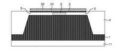
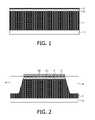
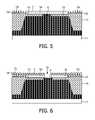
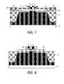
- FIGS. 1-8are schematic, cross-sectional views perpendicular to the thickness direction of a device, showing successive stages of the manufacture thereof by means of a method according to the invention.
- FIGS. 1-8are schematic, cross-sectional views perpendicular to the thickness direction of a device, showing successive stages of the manufacture thereof by means of a method according to the invention.
- the starting point(see FIG. 1 ) is an n-type silicon substrate 11 , on which a first silicon layer 1 , a SiGe layer 2 and a further silicon layer 3 are formed by epitaxy, wherein, in this example, all three layers ( 1 , 2 , 3 ) are n-type.
- An underlying part of the substrate 11has been left out of the drawing for the sake of simplicity.
- the SiGe layer 2has, in this example, a Ge content of 20% and a thickness of approximately 20 nm to 30 nm.
- the thickness of the further silicon layer 3is preferably in the range of 10 nm to 100 nm to enable, in a further stage of the process, the transformation of this second layer 3 into a base region.
- a silicon dioxide layer 31 and a silicon nitride layer 32are deposited and patterned to open up a window where STI (shallow trench isolation) cavities 4 are formed by etching of the further silicon layer 3 , the SiGe layer 2 and a portion of the first silicon layer 1 .
- the sidewalls of the STI cavities 4expose side faces of the second layer 3 , the SiGe layer 2 and a part thereof of the first silicon layer 1 .
- part of the SiGe layer 2is removed from the side walls of the STI cavities 4 by means of a selective—wet or dry—chemical etching process. Buried cavities 5 are thereby formed adjacent to the STI cavities 4 and to the remaining part of the SiGe layer 2 .
- the side of the remaining part of the SiGe layer 2is, in this example, approximately 100 nm to 200 nm from the sidewall of the STI region 4 .
- a thermal oxidation stepis done that fills the buried cavities 5 with silicon dioxide, thereby forming buried isolation regions 15 .
- the thermal oxidationis done at a temperature of about 900° C. to 1050° C.
- An advantageous result of this thermal oxidation stepis that the SiGe layer 2 is transformed into a layer with relatively less Ge than the SiGe layer 2 , because a part of the Ge atoms of the SiGe layer 2 are thermally diffused to the surrounding first and further silicon layers 1 , 3 .
- the Ge content of the SiGe layer 2will be reduced to lower than 10% and the Ge-rich SiGe layer 2 , which could disadvantageously influence the to be fabricated bipolar transistor, is as such no longer part of the collector region of the to be fabricated bipolar transistor due to the out diffusion of Ge.
- the to be fabricated bipolar transistordoes not comprise the Ge-rich SiGe layer 2 , which, as being part of a to be fabricated collector region, advantageously influences the performance of the to be fabricated bipolar transistor.
- the remaining part of the STI cavities 4is filled with an isolation material, which is not necessarily the same material with which the buried cavities 5 are filled, such as silicon dioxide, using commonly known techniques, such as, for example, HDP (High Density Plasma) oxide and CMP (Chemical Mechanical Planarization), thereby forming STI regions 14 .
- an insulation layeris formed on the exposed surfaces of the STI cavities 4 , after which the STI cavities 4 are not filled with a solid or liquid material, but instead are filled with a gas, for example air, or are made vacuum, thus creating vacuum STI regions. This advantageously improves the isolation properties of the STI regions.
- the silicon dioxide layer 31 and the silicon nitride layer 32are removed using standard etching techniques.
- a protective seed layer 33is formed using photolithographic patterning and etching techniques, defining a window where a bipolar transistor will be formed and which at the same protects a region where, for example, standard CMOS devices are formed.
- a base layer 7is formed which has a monocrystalline silicon part 7 B formed on silicon regions and a polycrystalline silicon part 7 A formed on other regions.
- the further silicon layer 3is now transformed in to a part of the monocrystalline part 7 B of the base layer 7 , and hence the base layer 7 adjoins the buried isolation region 15 .
- a collector region 6is defined which comprises the remaining parts of the first silicon layer 1 and the SiGe layer 2 that are in between the buried isolation regions 15 and the STI cavities 4 .
- an insulation layer 34is formed, for example by deposition of silicon dioxide, and an emitter opening 35 is formed by photolithographic patterning and etching techniques.
- the emitter opening 35is filled with an, in this case, n-type polycrystalline silicon layer thereby forming an emitter connection region 8 .
- Said layeris formed by means of a CVD process.
- an emitter region 9is formed in a part of the base layer 7 by local over doping as a result of out diffusion of the n-type contaminations from the emitter connection region 8 into the base layer 7 .
- the emitter connection region 8is patterned by photolithography and etching, obtaining a T-shaped cross-section for the emitter connection region 8 .
- the base layer 7is patterned and etched, and emitter spacers 36 are formed. Thereafter, connecting conductors are formed that electrically connect to the bipolar transistor regions (not shown in the Figures).
- the inventionprovides a method of manufacturing a bipolar transistor on a semiconductor substrate which is provided with a first, a second and a third layer of a first, second and third semiconductor material respectively, all of a first conductivity type.
- a first portion of the second layeris transformed into a buried isolation region comprising a first electrically insulating material.
- a first semiconductor region of the first conductivity typecomprising, for example, a collector region, is formed from a second portion of the second layer adjoining the buried isolation region and a portion of the first layer adjoining the second portion of the second layer.
- a base regionis formed on the buried isolation region and on the first semiconductor region by transforming the third layer into a second conductivity type, which is opposite to the first conductivity type.
- a second semiconductor region of the first conductivity typecomprising, for example, an emitter region, is formed on a part of the base region.
- the inventionis not limited to the embodiments as discussed herein, as many variations and modifications are possible to those skilled in the art within the scope of the invention.
- BICMOSBipolar
- Complementary Metal Oxide SemiconductorIntegrated Circuit
- the method according to the inventioncan also be advantageously be combined with the formation of PiFETs (Partly Insulated Field Effect Transistors).
- PiFETsPartly Insulated Field Effect Transistors
- SiGesilicon germanium carbide
- SiCsilicon carbide
- siliconmay also be provided with contaminations which hardly affect the grid constant of silicon but which nevertheless enable selective etching.
- n-type siliconcan be selectively etched with respect to p-type silicon, for example, or vice versa.
- an electrically non-active do pantmay influence the etchability of silicon to a sufficient extent.
- the SiGe layer or a SiGe regioncan also be formed by implanting germanium in a silicon region.
Landscapes
- Bipolar Transistors (AREA)
Abstract
Description
- The invention relates to a method of manufacturing a bipolar transistor.
- Semiconductor technologies have seen a tremendous increase in the cutoff frequency and maximum frequency of oscillation over the past decade. These figures of merit have increased from tens of GHz to hundreds of GHz. This development has been achieved predominantly as a result of an increased current drive of the applied bipolar transistors.
- There is a fundamental tradeoff between the maximum current drive and the collector to base capacitance of a bipolar transistor. To achieve a high cutoff frequency and the high current drive, a high doping level in the collector region is required, which disadvantageously increases the collector to base capacitance considerably. The collector to base capacitance introduces a disadvantageous parasitic feedback in the device that limits the gain of the bipolar transistor. Therefore, the collector to base capacitance should be as low as possible, of course without affecting current drive and cutoff frequency.
- An npn-type bipolar transistor with a high cutoff frequency is disclosed in US2004/0224461 in which the bipolar transistor comprises a mesa-shaped emitter region on top of a layered base region, and a collector region there under. The junction between the base region and the collector region is surrounded by an electrically insulating region which is buried under the base region and which forms a local constriction of the semiconductor body.
- The bipolar transistor comprises intrinsic and extrinsic regions. The intrinsic regions of the bipolar transistor are the regions that are required for the (intrinsic) operation of the bipolar transistor. The extrinsic regions are not required for the (intrinsic) operation of the bipolar transistor, but these extrinsic regions are present because the bipolar transistor in practice requires some measures to be able to operate, such as, for example, electrical connections to the base and collector regions, which electrical connections normally cannot be made directly on the intrinsic region of the base and collector regions. A drawback of the known bipolar transistor is that it comprises a collector to base capacitance with an extrinsic region that disadvantageously decreases the high frequency performance of the known bipolar transistor.
- It is an object of the present invention to provide a method of fabricating a bipolar transistor in which the capacitance, introduced by the extrinsic region, is reduced. The invention provides a method as claimed in
claim 1. Advantageous embodiments are defined by the dependent claims. - The method of manufacturing a bipolar transistor according to the invention on a semiconductor substrate comprises the steps of:
- forming on the semiconductor substrate a first, a second and a third layer of a first, second and third semiconductor material respectively, all of a first conductivity type;
- transforming a first portion of the second layer into a buried isolation region comprising a first electrically insulating material;
- forming a first semiconductor region of the first conductivity type, comprising a collector region or an emitter region, from a second portion of the second layer adjoining the buried isolation region and a portion of the first layer adjoining the second portion of the second layer;
- forming a base region on the buried isolation region and on the first semiconductor region by transforming the third layer into a layer of a second conductivity type, which is opposite to the first conductivity type; and
- forming a second semiconductor region of the first conductivity type, comprising the other of said collector region and said emitter region, on a part of the base region.
- The invention provides for a fabrication method of a bipolar transistor in which the extrinsic capacitance between the first semiconductor region and the base region is decreased, because of the buried insulating layer in the first semiconductor region on which layer and region the base region is formed. The extrinsic first semiconductor region to base region capacitance is decreased by the fact that the value of this capacitance is now partly determined by the buried insulating layer, which has a substantially lower dielectric constant than that of the first semiconductor region to base region junction. For example, a capacitance is achieved that is lowered by a factor of two or more depending, amongst others, on the thickness of the buried isolation region. Furthermore, the value of the first semiconductor region to base region capacitance is less dependant on the doping levels of the first semiconductor region and the base region, which enables an increase of the doping levels of one or both of these regions to improve the performance of the bipolar transistor without increasing the extrinsic capacitance formed by the first semiconductor region to base region. Another advantage is that the buried isolation region is a diffusion barrier for dopants in the extrinsic part of the base region, which enables a higher doping level for the extrinsic base region without resulting in a too deep first semiconductor region to base region junction. Yet another advantage is that the injection of charge carriers from the base region into the first semiconductor region, and vice versa, is suppressed in the area where the buried isolation region is inserted. This ultimately leads to a further improved high-frequency performance of the bipolar transistor.
- It is noted in this connection that when the emitter region and the collector region exchange roles in a conventional bipolar transistor, the transistor is called an inverted transistor. In the device according to the invention, too, the emitter region may be positioned under the base region in a corresponding manner.
- A method to fabricate a buried insulating layer in a Field Effect Transistor (FET) device is known as such from the publication entitled “A Partially Insulated Field-Effect Transistor (PiFET) as a Candidate for Scaled Transistors” by Kyoung Hwan Yeo et al. that has been published in IEEE Electron Device Letters, vol. 25 no. 6, June 2004. In this publication a SiGe layer is deposited epitaxially on a semiconductor substrate and on said layer a silicon layer is deposited. A mask is provided on the silicon layer, which is provided with an opening. In the opening both the silicon layer and the SiGe layer are removed by etching. Subsequently, after removal of the mask, a further silicon layer is provided in the etched opening in the silicon and SiGe layer. In this way, a SiGe region buried by a silicon layer is obtained. The SiGe region is then removed by selective etching and replaced by an insulating material, e.g. a silicon dioxide. A FET is then formed above two of such regions in which the SiGe has been replaced by silicon dioxide and which are separated by a silicon region. In this way a partially insulated FET is obtained. This known method provides for a buried isolation region in a FET device, whereas the method according to the invention provides a bipolar transistor by combining the formation of the buried isolation region with the formation of the first semiconductor region, comprising for example the collector region, and the transformation of the conductivity type of the third layer into the opposite conductivity type, thereby forming the base region of the bipolar transistor.
- In a favorable embodiment of the method according to the invention, the step of transforming the first portion of the second layer into the buried isolation region is characterized by the steps of:
- providing an opening which exposes a part of the second layer;
- removing a portion of the second layer selectively with respect to the first and the third layer, thereby forming a cavity between the first and the third layer; and
- filling the cavity with the first electrically insulating material, thereby forming the buried isolation region.
- This method is a simple and robust way to manufacture the buried insulation region and may be integrated in a standard process flow, such as, for example, a CMOS (Complementary Metal Oxide Semiconductor) technology where the opening, for example, may be provided by a standard STI (Shallow Trench Isolation) region.
- In a preferred embodiment of a method according to the invention, the second semiconductor material comprises a mixed crystal of silicon and germanium, and the first and the third semiconductor material both comprise silicon. This advantageously enables the selective removal of a part of the second layer with respect to the first and third layer. In a further advantageous embodiment the step of forming the first semiconductor region comprises a thermal step after which most of the germanium is diffused out of the second layer. Because the first and the third layer comprise silicon, the thermal oxidation step enables the germanium comprised in the second layer to diffuse to the first and the third layer. Thereafter, the germanium is not concentrated in the second layer anymore, but spread out in the first, second and third layer in such a way that the influence of the silicon germanium on the performance of the bipolar transistor is reduced to an acceptable level.
- In a favorable embodiment according to the invention, the step of forming the base region is characterized by the step of epitaxial growth of a fourth layer of a second conductivity type on the third layer thereby transforming the third layer into the second conductivity type. This advantageously reduces the number of required process steps to obtain the base region.
- Preferably the third layer has a thickness in the range of 10 nanometers to 100 nanometers. This facilitates the formation of the base region in the part of the third layer, which is located on top of the buried isolation region.
- In a favorable embodiment according to the invention, a photolithographic step is applied before the step of transforming the first portion of the second layer into the buried isolation region, which photolithographic step opens regions where the first portion of the second layer is transformed. This enables the formation of regions where the buried isolation region does not need to be fabricated, for example in a region where a standard CMOS transistor is fabricated.
- Preferably the first, second and third layer are formed as part of an epitaxial layer. This advantageously reduces the number of required process steps.
- In a favorable embodiment of a method according to the invention, the first semiconductor region comprises the collector region and the second semiconductor region comprises the emitter region.
- The invention will now be explained in more detail with reference to an embodiment and the drawing, in which:
FIGS. 1-8 are schematic, cross-sectional views perpendicular to the thickness direction of a device, showing successive stages of the manufacture thereof by means of a method according to the invention.- The Figures are not drawn to scale, and some dimensions are exaggerated for the sake of clarity. Like regions or parts are indicated by the same numerals as much as possible.
FIGS. 1-8 are schematic, cross-sectional views perpendicular to the thickness direction of a device, showing successive stages of the manufacture thereof by means of a method according to the invention.- The starting point (see
FIG. 1 ) is an n-type silicon substrate 11, on which afirst silicon layer 1, aSiGe layer 2 and afurther silicon layer 3 are formed by epitaxy, wherein, in this example, all three layers (1,2,3) are n-type. An underlying part of thesubstrate 11 has been left out of the drawing for the sake of simplicity. TheSiGe layer 2 has, in this example, a Ge content of 20% and a thickness of approximately 20 nm to 30 nm. The thickness of thefurther silicon layer 3 is preferably in the range of 10 nm to 100 nm to enable, in a further stage of the process, the transformation of thissecond layer 3 into a base region. - Thereafter (see
FIG. 2 ), asilicon dioxide layer 31 and asilicon nitride layer 32 are deposited and patterned to open up a window where STI (shallow trench isolation)cavities 4 are formed by etching of thefurther silicon layer 3, theSiGe layer 2 and a portion of thefirst silicon layer 1. The sidewalls of theSTI cavities 4 expose side faces of thesecond layer 3, theSiGe layer 2 and a part thereof of thefirst silicon layer 1. - Subsequently (see
FIG. 3 ), part of theSiGe layer 2 is removed from the side walls of theSTI cavities 4 by means of a selective—wet or dry—chemical etching process.Buried cavities 5 are thereby formed adjacent to theSTI cavities 4 and to the remaining part of theSiGe layer 2. The side of the remaining part of theSiGe layer 2 is, in this example, approximately 100 nm to 200 nm from the sidewall of theSTI region 4. - Then (see
FIG. 4 ) a thermal oxidation step is done that fills the buriedcavities 5 with silicon dioxide, thereby forming buriedisolation regions 15. The thermal oxidation is done at a temperature of about 900° C. to 1050° C. An advantageous result of this thermal oxidation step is that theSiGe layer 2 is transformed into a layer with relatively less Ge than theSiGe layer 2, because a part of the Ge atoms of theSiGe layer 2 are thermally diffused to the surrounding first andfurther silicon layers SiGe layer 2 will be reduced to lower than 10% and the Ge-rich SiGe layer 2, which could disadvantageously influence the to be fabricated bipolar transistor, is as such no longer part of the collector region of the to be fabricated bipolar transistor due to the out diffusion of Ge. Hence, the to be fabricated bipolar transistor does not comprise the Ge-rich SiGe layer 2, which, as being part of a to be fabricated collector region, advantageously influences the performance of the to be fabricated bipolar transistor. Then the remaining part of theSTI cavities 4 is filled with an isolation material, which is not necessarily the same material with which the buriedcavities 5 are filled, such as silicon dioxide, using commonly known techniques, such as, for example, HDP (High Density Plasma) oxide and CMP (Chemical Mechanical Planarization), thereby formingSTI regions 14. In an alternative embodiment, an insulation layer is formed on the exposed surfaces of theSTI cavities 4, after which theSTI cavities 4 are not filled with a solid or liquid material, but instead are filled with a gas, for example air, or are made vacuum, thus creating vacuum STI regions. This advantageously improves the isolation properties of the STI regions. - Thereafter (see
FIG. 5 ), thesilicon dioxide layer 31 and thesilicon nitride layer 32 are removed using standard etching techniques. Aprotective seed layer 33 is formed using photolithographic patterning and etching techniques, defining a window where a bipolar transistor will be formed and which at the same protects a region where, for example, standard CMOS devices are formed. By applying epitaxy of silicon, abase layer 7 is formed which has amonocrystalline silicon part 7B formed on silicon regions and apolycrystalline silicon part 7A formed on other regions. Thefurther silicon layer 3 is now transformed in to a part of themonocrystalline part 7B of thebase layer 7, and hence thebase layer 7 adjoins the buriedisolation region 15. At this point acollector region 6 is defined which comprises the remaining parts of thefirst silicon layer 1 and theSiGe layer 2 that are in between the buriedisolation regions 15 and theSTI cavities 4. - Now (see
FIG. 6 ) aninsulation layer 34 is formed, for example by deposition of silicon dioxide, and anemitter opening 35 is formed by photolithographic patterning and etching techniques. - Following this (see
FIG. 7 ) theemitter opening 35 is filled with an, in this case, n-type polycrystalline silicon layer thereby forming anemitter connection region 8. Said layer is formed by means of a CVD process. By subjecting the resulting structure to a heat treatment, anemitter region 9 is formed in a part of thebase layer 7 by local over doping as a result of out diffusion of the n-type contaminations from theemitter connection region 8 into thebase layer 7. Then theemitter connection region 8 is patterned by photolithography and etching, obtaining a T-shaped cross-section for theemitter connection region 8. - Subsequently (see
FIG. 8 ), thebase layer 7 is patterned and etched, andemitter spacers 36 are formed. Thereafter, connecting conductors are formed that electrically connect to the bipolar transistor regions (not shown in the Figures). - In summary, the invention provides a method of manufacturing a bipolar transistor on a semiconductor substrate which is provided with a first, a second and a third layer of a first, second and third semiconductor material respectively, all of a first conductivity type. A first portion of the second layer is transformed into a buried isolation region comprising a first electrically insulating material. A first semiconductor region of the first conductivity type, comprising, for example, a collector region, is formed from a second portion of the second layer adjoining the buried isolation region and a portion of the first layer adjoining the second portion of the second layer. Then a base region is formed on the buried isolation region and on the first semiconductor region by transforming the third layer into a second conductivity type, which is opposite to the first conductivity type. Thereafter a second semiconductor region of the first conductivity type, comprising, for example, an emitter region, is formed on a part of the base region. This method provides for the formation of a bipolar transistor, with an advantageous decrease of the extrinsic collector to base region capacitance by the fact that the value of this capacitance is mainly determined by the buried isolation region which has a substantially lower dielectric constant than that of the collector to base region junction.
- The invention is not limited to the embodiments as discussed herein, as many variations and modifications are possible to those skilled in the art within the scope of the invention. Thus, in addition to being suitable for use in a discrete semiconductor device, the invention is also very suitable for use in an integrated semiconductor device, such as a (BI)CMOS (=(Bipolar) Complementary Metal Oxide Semiconductor) IC (=Integrated Circuit). The method according to the invention can also be advantageously be combined with the formation of PiFETs (Partly Insulated Field Effect Transistors). In fact, the structure and the manufacture of the transistor as described in the examples is quite suitable for use in an IC.
- Furthermore it is noted that besides SiGe, it is also possible to use other materials which can be selectively etched and on which silicon monocrystalline can be grown. An example of such a material is SiC. In addition to that, silicon may also be provided with contaminations which hardly affect the grid constant of silicon but which nevertheless enable selective etching. Thus, n-type silicon can be selectively etched with respect to p-type silicon, for example, or vice versa. Furthermore, an electrically non-active do pant may influence the etchability of silicon to a sufficient extent.
- Many variants and modifications are possible also with regard to a method according to the invention. Thus, the SiGe layer or a SiGe region can also be formed by implanting germanium in a silicon region.
- In the claims, any reference signs between parentheses shall not be construed as limiting the scope. The indefinite article “a” or “an” does not exclude the presence of a plurality. Features recited in mutually different dependent claims may be combined.
Claims (9)
Applications Claiming Priority (6)
| Application Number | Priority Date | Filing Date | Title |
|---|---|---|---|
| EP06110950 | 2006-03-10 | ||
| EP06110950.0 | 2006-03-10 | ||
| EP06110950 | 2006-03-10 | ||
| PCT/IB2007/050786WO2007105155A1 (en) | 2006-03-10 | 2007-03-09 | Method of manufacturing a bipolar transistor |
| WOPCT/IB2007/050786 | 2007-03-09 | ||
| WOIB/PCT2007/050786 | 2007-03-09 |
Publications (2)
| Publication Number | Publication Date |
|---|---|
| US20090053872A1true US20090053872A1 (en) | 2009-02-26 |
| US7838374B2 US7838374B2 (en) | 2010-11-23 |
Family
ID=38282793
Family Applications (1)
| Application Number | Title | Priority Date | Filing Date |
|---|---|---|---|
| US12/282,300Expired - Fee RelatedUS7838374B2 (en) | 2006-03-10 | 2007-03-09 | Method of manufacturing a bipolar transistor |
Country Status (6)
| Country | Link |
|---|---|
| US (1) | US7838374B2 (en) |
| EP (1) | EP1997130B1 (en) |
| JP (1) | JP2009526396A (en) |
| CN (1) | CN101467237B (en) |
| TW (1) | TW200809980A (en) |
| WO (1) | WO2007105155A1 (en) |
Cited By (1)
| Publication number | Priority date | Publication date | Assignee | Title |
|---|---|---|---|---|
| US20140193960A1 (en)* | 2009-11-30 | 2014-07-10 | Fujitsu Semiconductor Limited | Fabrication method of semiconductor device and fabrication method of dynamic threshold transistor |
Families Citing this family (5)
| Publication number | Priority date | Publication date | Assignee | Title |
|---|---|---|---|---|
| WO2009141753A1 (en)* | 2008-05-21 | 2009-11-26 | Nxp B.V. | A method of manufacturing a bipolar transistor semiconductor device and semiconductor devices obtained thereby |
| JP5643635B2 (en)* | 2010-12-24 | 2014-12-17 | 旭化成エレクトロニクス株式会社 | Manufacturing method of semiconductor device |
| US8610174B2 (en)* | 2011-11-30 | 2013-12-17 | International Business Machines Corporation | Bipolar transistor with a raised collector pedestal for reduced capacitance |
| US8603889B2 (en)* | 2012-03-30 | 2013-12-10 | International Business Machines Corporation | Integrated circuit structure having air-gap trench isolation and related design structure |
| US9029229B2 (en)* | 2013-05-29 | 2015-05-12 | International Business Machines Corporation | Semiconductor device and method of forming the device by forming monocrystalline semiconductor layers on a dielectric layer over isolation regions |
Citations (7)
| Publication number | Priority date | Publication date | Assignee | Title |
|---|---|---|---|---|
| US5439832A (en)* | 1993-06-04 | 1995-08-08 | Fujitsu Limited | Method for fabricating semiconductor device |
| US5620907A (en)* | 1995-04-10 | 1997-04-15 | Lucent Technologies Inc. | Method for making a heterojunction bipolar transistor |
| US20010028093A1 (en)* | 2000-03-30 | 2001-10-11 | Kazuo Yamazaki | Fabrication method for semiconductor integrated circuit devices and semiconductor integrated circuit device |
| US6395608B2 (en)* | 1998-01-26 | 2002-05-28 | Lg Electronics Inc. | Heterojunction bipolar transistor and its fabrication method |
| US20040188797A1 (en)* | 2003-03-28 | 2004-09-30 | International Business Machines Corporation | Bipolar transistor structure and methods using shallow isolation extension to reduce parasitic capacitance |
| US20040224461A1 (en)* | 2003-05-09 | 2004-11-11 | International Business Machines Corporation | Method to fabricate high-performance NPN transistors in a BiCMOS process |
| US20040262715A1 (en)* | 2003-06-19 | 2004-12-30 | Makoto Miura | Semiconductor device and manufacturing method for the same |
Family Cites Families (10)
| Publication number | Priority date | Publication date | Assignee | Title |
|---|---|---|---|---|
| JPH04312927A (en)* | 1991-03-18 | 1992-11-04 | Mitsubishi Electric Corp | Semiconductor device and its manufacturing method |
| JP2980497B2 (en)* | 1993-11-15 | 1999-11-22 | 株式会社東芝 | Method of manufacturing dielectric-isolated bipolar transistor |
| EP0818829A1 (en) | 1996-07-12 | 1998-01-14 | Hitachi, Ltd. | Bipolar transistor and method of fabricating it |
| FR2800197B1 (en) | 1999-10-25 | 2003-02-07 | St Microelectronics Sa | METHOD FOR DEFINING TWO SELF-ALIGNED AREAS ON THE UPPER SURFACE OF A SUBSTRATE |
| FR2805924A1 (en) | 2000-03-06 | 2001-09-07 | France Telecom | Polycrystalline silicon layer etching process used in production of emitter self-aligned with extrinsic base of bipolar transistor involves stopping plasma-etching on or in germanium or silicon-germanium intermediate layer, to form grooves |
| JP2002184783A (en)* | 2000-12-14 | 2002-06-28 | Nec Yamagata Ltd | Method for manufacturing semiconductor device |
| US6767798B2 (en)* | 2002-04-09 | 2004-07-27 | Maxim Integrated Products, Inc. | Method of forming self-aligned NPN transistor with raised extrinsic base |
| JP2004087703A (en)* | 2002-08-26 | 2004-03-18 | Alps Electric Co Ltd | Method for manufacturing semiconductor integrated circuit device |
| JP4014548B2 (en)* | 2003-09-17 | 2007-11-28 | 沖電気工業株式会社 | Semiconductor device and manufacturing method thereof |
| US6979884B2 (en)* | 2003-12-04 | 2005-12-27 | International Business Machines Corporation | Bipolar transistor having self-aligned silicide and a self-aligned emitter contact border |
- 2007
- 2007-03-07TWTW096107953Apatent/TW200809980A/enunknown
- 2007-03-09EPEP07713227.2Apatent/EP1997130B1/ennot_activeNot-in-force
- 2007-03-09CNCN2007800086890Apatent/CN101467237B/ennot_activeExpired - Fee Related
- 2007-03-09USUS12/282,300patent/US7838374B2/ennot_activeExpired - Fee Related
- 2007-03-09JPJP2008553882Apatent/JP2009526396A/enactivePending
- 2007-03-09WOPCT/IB2007/050786patent/WO2007105155A1/enactiveApplication Filing
Patent Citations (7)
| Publication number | Priority date | Publication date | Assignee | Title |
|---|---|---|---|---|
| US5439832A (en)* | 1993-06-04 | 1995-08-08 | Fujitsu Limited | Method for fabricating semiconductor device |
| US5620907A (en)* | 1995-04-10 | 1997-04-15 | Lucent Technologies Inc. | Method for making a heterojunction bipolar transistor |
| US6395608B2 (en)* | 1998-01-26 | 2002-05-28 | Lg Electronics Inc. | Heterojunction bipolar transistor and its fabrication method |
| US20010028093A1 (en)* | 2000-03-30 | 2001-10-11 | Kazuo Yamazaki | Fabrication method for semiconductor integrated circuit devices and semiconductor integrated circuit device |
| US20040188797A1 (en)* | 2003-03-28 | 2004-09-30 | International Business Machines Corporation | Bipolar transistor structure and methods using shallow isolation extension to reduce parasitic capacitance |
| US20040224461A1 (en)* | 2003-05-09 | 2004-11-11 | International Business Machines Corporation | Method to fabricate high-performance NPN transistors in a BiCMOS process |
| US20040262715A1 (en)* | 2003-06-19 | 2004-12-30 | Makoto Miura | Semiconductor device and manufacturing method for the same |
Cited By (2)
| Publication number | Priority date | Publication date | Assignee | Title |
|---|---|---|---|---|
| US20140193960A1 (en)* | 2009-11-30 | 2014-07-10 | Fujitsu Semiconductor Limited | Fabrication method of semiconductor device and fabrication method of dynamic threshold transistor |
| US9178034B2 (en)* | 2009-11-30 | 2015-11-03 | Fujitsu Semiconductor Limited | Fabrication method of semiconductor device and fabrication method of dynamic threshold transistor |
Also Published As
| Publication number | Publication date |
|---|---|
| CN101467237B (en) | 2011-01-12 |
| JP2009526396A (en) | 2009-07-16 |
| TW200809980A (en) | 2008-02-16 |
| CN101467237A (en) | 2009-06-24 |
| US7838374B2 (en) | 2010-11-23 |
| EP1997130B1 (en) | 2014-06-25 |
| EP1997130A1 (en) | 2008-12-03 |
| WO2007105155A1 (en) | 2007-09-20 |
Similar Documents
| Publication | Publication Date | Title |
|---|---|---|
| US7776704B2 (en) | Method to build self-aligned NPN in advanced BiCMOS technology | |
| US8067290B2 (en) | Bipolar transistor with base-collector-isolation without dielectric | |
| JP3494638B2 (en) | Semiconductor device and method of manufacturing semiconductor device | |
| CN101960584B (en) | Semiconductor device and method of manufacture thereof | |
| JP2005244224A (en) | Ultrathin soi bipolar transistor for low substrate bias action provided with inverted collector on thin embedded oxide film (box) and method of the same | |
| CN101256983A (en) | Semiconductor structures and methods | |
| JP2004241779A (en) | BiCMOS manufacturing method utilizing self-alignment | |
| US7932156B2 (en) | Bipolar transistor having a second, base-comprising region consisting of a first layer, a second, constrictive, layer, and a third layer | |
| US7838374B2 (en) | Method of manufacturing a bipolar transistor | |
| US8101491B2 (en) | Heterojunction bipolar transistor | |
| US8133791B2 (en) | Method of manufacturing a bipolar transistor and bipolar transistor obtained therewith | |
| JP2008538864A (en) | Bipolar transistor and manufacturing method thereof | |
| JP2002289834A (en) | Semiconductor device manufacturing method and semiconductor device | |
| KR101173526B1 (en) | A bipolar junction transistor having a high germanium concentration in a silicon-germanium layer and a method for forming the bipolar junction transistor | |
| US7285470B2 (en) | Method for the production of a bipolar semiconductor component, especially a bipolar transistor, and corresponding bipolar semiconductor component | |
| US7358132B2 (en) | Self-aligned bipolar semiconductor device and fabrication method thereof | |
| JP2001196382A (en) | Semiconductor device and manufacturing method thereof | |
| CN101257043A (en) | Semiconductor device and manufacturing method thereof | |
| JP2005057171A (en) | Semiconductor device and manufacturing method thereof | |
| JP3908023B2 (en) | Manufacturing method of semiconductor device | |
| JP2004273558A (en) | Manufacturing method of bipolar transistor | |
| JPH0621071A (en) | Method for manufacturing semiconductor device | |
| JP2002368002A (en) | Semiconductor device and manufacturing method thereof | |
| JP2004253502A (en) | Bipolar transistor and method of manufacturing the same | |
| JP2005101107A (en) | Semiconductor device and manufacturing method thereof |
Legal Events
| Date | Code | Title | Description |
|---|---|---|---|
| AS | Assignment | Owner name:NXP, B.V., NETHERLANDS Free format text:ASSIGNMENT OF ASSIGNORS INTEREST;ASSIGNORS:VAN NOORT, WIBO D;SONSKY, JAN;PIONTEK, ANDREAS M.;REEL/FRAME:021503/0400;SIGNING DATES FROM 20080312 TO 20080908 | |
| STCF | Information on status: patent grant | Free format text:PATENTED CASE | |
| FPAY | Fee payment | Year of fee payment:4 | |
| AS | Assignment | Owner name:MORGAN STANLEY SENIOR FUNDING, INC., MARYLAND Free format text:SECURITY AGREEMENT SUPPLEMENT;ASSIGNOR:NXP B.V.;REEL/FRAME:038017/0058 Effective date:20160218 | |
| AS | Assignment | Owner name:MORGAN STANLEY SENIOR FUNDING, INC., MARYLAND Free format text:CORRECTIVE ASSIGNMENT TO CORRECT THE REMOVE APPLICATION 12092129 PREVIOUSLY RECORDED ON REEL 038017 FRAME 0058. ASSIGNOR(S) HEREBY CONFIRMS THE SECURITY AGREEMENT SUPPLEMENT;ASSIGNOR:NXP B.V.;REEL/FRAME:039361/0212 Effective date:20160218 | |
| AS | Assignment | Owner name:MORGAN STANLEY SENIOR FUNDING, INC., MARYLAND Free format text:CORRECTIVE ASSIGNMENT TO CORRECT THE REMOVE APPLICATION 12681366 PREVIOUSLY RECORDED ON REEL 039361 FRAME 0212. ASSIGNOR(S) HEREBY CONFIRMS THE SECURITY AGREEMENT SUPPLEMENT;ASSIGNOR:NXP B.V.;REEL/FRAME:042762/0145 Effective date:20160218 Owner name:MORGAN STANLEY SENIOR FUNDING, INC., MARYLAND Free format text:CORRECTIVE ASSIGNMENT TO CORRECT THE REMOVE APPLICATION 12681366 PREVIOUSLY RECORDED ON REEL 038017 FRAME 0058. ASSIGNOR(S) HEREBY CONFIRMS THE SECURITY AGREEMENT SUPPLEMENT;ASSIGNOR:NXP B.V.;REEL/FRAME:042985/0001 Effective date:20160218 | |
| MAFP | Maintenance fee payment | Free format text:PAYMENT OF MAINTENANCE FEE, 8TH YEAR, LARGE ENTITY (ORIGINAL EVENT CODE: M1552) Year of fee payment:8 | |
| AS | Assignment | Owner name:INTERUNIVERSITAIR MICROELEKTRONICA CENTRUM VZM, BE Free format text:CORRECTIVE ASSIGNMENT TO CORRECT THE ASSIGNEE'S DATA PREVIOUSLY RECORDED ON REEL 021503 FRAME 0400. ASSIGNOR(S) HEREBY CONFIRMS THE ASSIGNMENT;ASSIGNORS:VAN NOORT, WIBO D.;SONSKY, JAN;PIONTEK, ANDREAS M.;SIGNING DATES FROM 20080312 TO 20080908;REEL/FRAME:046322/0600 Owner name:NXP B.V., NETHERLANDS Free format text:CORRECTIVE ASSIGNMENT TO CORRECT THE ASSIGNEE'S DATA PREVIOUSLY RECORDED ON REEL 021503 FRAME 0400. ASSIGNOR(S) HEREBY CONFIRMS THE ASSIGNMENT;ASSIGNORS:VAN NOORT, WIBO D.;SONSKY, JAN;PIONTEK, ANDREAS M.;SIGNING DATES FROM 20080312 TO 20080908;REEL/FRAME:046322/0600 | |
| AS | Assignment | Owner name:NXP B.V., NETHERLANDS Free format text:RELEASE BY SECURED PARTY;ASSIGNOR:MORGAN STANLEY SENIOR FUNDING, INC.;REEL/FRAME:050745/0001 Effective date:20190903 | |
| AS | Assignment | Owner name:MORGAN STANLEY SENIOR FUNDING, INC., MARYLAND Free format text:CORRECTIVE ASSIGNMENT TO CORRECT THE REMOVE APPLICATION 12298143 PREVIOUSLY RECORDED ON REEL 042762 FRAME 0145. ASSIGNOR(S) HEREBY CONFIRMS THE SECURITY AGREEMENT SUPPLEMENT;ASSIGNOR:NXP B.V.;REEL/FRAME:051145/0184 Effective date:20160218 Owner name:MORGAN STANLEY SENIOR FUNDING, INC., MARYLAND Free format text:CORRECTIVE ASSIGNMENT TO CORRECT THE REMOVE APPLICATION 12298143 PREVIOUSLY RECORDED ON REEL 039361 FRAME 0212. ASSIGNOR(S) HEREBY CONFIRMS THE SECURITY AGREEMENT SUPPLEMENT;ASSIGNOR:NXP B.V.;REEL/FRAME:051029/0387 Effective date:20160218 Owner name:MORGAN STANLEY SENIOR FUNDING, INC., MARYLAND Free format text:CORRECTIVE ASSIGNMENT TO CORRECT THE REMOVE APPLICATION 12298143 PREVIOUSLY RECORDED ON REEL 042985 FRAME 0001. ASSIGNOR(S) HEREBY CONFIRMS THE SECURITY AGREEMENT SUPPLEMENT;ASSIGNOR:NXP B.V.;REEL/FRAME:051029/0001 Effective date:20160218 Owner name:MORGAN STANLEY SENIOR FUNDING, INC., MARYLAND Free format text:CORRECTIVE ASSIGNMENT TO CORRECT THE REMOVE APPLICATION12298143 PREVIOUSLY RECORDED ON REEL 042985 FRAME 0001. ASSIGNOR(S) HEREBY CONFIRMS THE SECURITY AGREEMENT SUPPLEMENT;ASSIGNOR:NXP B.V.;REEL/FRAME:051029/0001 Effective date:20160218 Owner name:MORGAN STANLEY SENIOR FUNDING, INC., MARYLAND Free format text:CORRECTIVE ASSIGNMENT TO CORRECT THE REMOVE APPLICATION 12298143 PREVIOUSLY RECORDED ON REEL 038017 FRAME 0058. ASSIGNOR(S) HEREBY CONFIRMS THE SECURITY AGREEMENT SUPPLEMENT;ASSIGNOR:NXP B.V.;REEL/FRAME:051030/0001 Effective date:20160218 Owner name:MORGAN STANLEY SENIOR FUNDING, INC., MARYLAND Free format text:CORRECTIVE ASSIGNMENT TO CORRECT THE REMOVE APPLICATION12298143 PREVIOUSLY RECORDED ON REEL 039361 FRAME 0212. ASSIGNOR(S) HEREBY CONFIRMS THE SECURITY AGREEMENT SUPPLEMENT;ASSIGNOR:NXP B.V.;REEL/FRAME:051029/0387 Effective date:20160218 Owner name:MORGAN STANLEY SENIOR FUNDING, INC., MARYLAND Free format text:CORRECTIVE ASSIGNMENT TO CORRECT THE REMOVE APPLICATION12298143 PREVIOUSLY RECORDED ON REEL 042762 FRAME 0145. ASSIGNOR(S) HEREBY CONFIRMS THE SECURITY AGREEMENT SUPPLEMENT;ASSIGNOR:NXP B.V.;REEL/FRAME:051145/0184 Effective date:20160218 | |
| FEPP | Fee payment procedure | Free format text:MAINTENANCE FEE REMINDER MAILED (ORIGINAL EVENT CODE: REM.); ENTITY STATUS OF PATENT OWNER: LARGE ENTITY | |
| LAPS | Lapse for failure to pay maintenance fees | Free format text:PATENT EXPIRED FOR FAILURE TO PAY MAINTENANCE FEES (ORIGINAL EVENT CODE: EXP.); ENTITY STATUS OF PATENT OWNER: LARGE ENTITY | |
| STCH | Information on status: patent discontinuation | Free format text:PATENT EXPIRED DUE TO NONPAYMENT OF MAINTENANCE FEES UNDER 37 CFR 1.362 | |
| FP | Lapsed due to failure to pay maintenance fee | Effective date:20221123 |