US20090047747A1 - Method of forming an amorphous ferroelectric memory device - Google Patents
Method of forming an amorphous ferroelectric memory deviceDownload PDFInfo
- Publication number
- US20090047747A1 US20090047747A1US12/217,657US21765708AUS2009047747A1US 20090047747 A1US20090047747 A1US 20090047747A1US 21765708 AUS21765708 AUS 21765708AUS 2009047747 A1US2009047747 A1US 2009047747A1
- Authority
- US
- United States
- Prior art keywords
- forming
- ferroelectric material
- act
- amorphous ferroelectric
- amorphous
- Prior art date
- Legal status (The legal status is an assumption and is not a legal conclusion. Google has not performed a legal analysis and makes no representation as to the accuracy of the status listed.)
- Granted
Links
Images


Classifications
- H—ELECTRICITY
- H10—SEMICONDUCTOR DEVICES; ELECTRIC SOLID-STATE DEVICES NOT OTHERWISE PROVIDED FOR
- H10D—INORGANIC ELECTRIC SEMICONDUCTOR DEVICES
- H10D1/00—Resistors, capacitors or inductors
- H10D1/60—Capacitors
- H10D1/68—Capacitors having no potential barriers
- H10D1/682—Capacitors having no potential barriers having dielectrics comprising perovskite structures
- G—PHYSICS
- G11—INFORMATION STORAGE
- G11C—STATIC STORES
- G11C11/00—Digital stores characterised by the use of particular electric or magnetic storage elements; Storage elements therefor
- G11C11/21—Digital stores characterised by the use of particular electric or magnetic storage elements; Storage elements therefor using electric elements
- G11C11/22—Digital stores characterised by the use of particular electric or magnetic storage elements; Storage elements therefor using electric elements using ferroelectric elements
- H—ELECTRICITY
- H10—SEMICONDUCTOR DEVICES; ELECTRIC SOLID-STATE DEVICES NOT OTHERWISE PROVIDED FOR
- H10B—ELECTRONIC MEMORY DEVICES
- H10B51/00—Ferroelectric RAM [FeRAM] devices comprising ferroelectric memory transistors
- H—ELECTRICITY
- H10—SEMICONDUCTOR DEVICES; ELECTRIC SOLID-STATE DEVICES NOT OTHERWISE PROVIDED FOR
- H10B—ELECTRONIC MEMORY DEVICES
- H10B53/00—Ferroelectric RAM [FeRAM] devices comprising ferroelectric memory capacitors
- H—ELECTRICITY
- H10—SEMICONDUCTOR DEVICES; ELECTRIC SOLID-STATE DEVICES NOT OTHERWISE PROVIDED FOR
- H10D—INORGANIC ELECTRIC SEMICONDUCTOR DEVICES
- H10D64/00—Electrodes of devices having potential barriers
- H10D64/01—Manufacture or treatment
- H10D64/031—Manufacture or treatment of data-storage electrodes
- H10D64/033—Manufacture or treatment of data-storage electrodes comprising ferroelectric layers
Definitions
- This inventionrelates to ferroelectric memory devices and methods of forming the same.
- Ferroelectric memory devicesuse ferroelectric materials to store information. These materials can store information by retaining a polarization state after exposure to an electric field.
- Some of these deviceshave a sheet of ferroelectric material layered over a conductive layer.
- a writing devicesuch as a plate or point, can be used to expose regions of the ferroelectric sheet to an electric field.
- the plate or pointacts to create an electric field in the region by placing a charge over the region opposite the conductive layer. This region is polarized, the polarization state is then retained after the electric field dissipates.
- the surface charge of the regioncan later be read by a reading device.
- the reading devicemoves another plate or point over the ferroelectric sheet, thereby reading the polarization state of the regions.
- ferroelectric memory devicesuse polycrystalline ferroelectric materials to store information. These polycrystalline materials have a grain structure that can make reading their polarization state difficult. This is especially true when reading small regions of the polycrystalline materials because each small region often has a small number of grains. For a region having few grains, the noise from the grain structure interferes with accurate measurement of the region's polarization state.
- ferroelectric memory devicesare physically integrated with integrated circuits (ICs).
- ICsintegrated circuits
- Polycrystalline ferroelectric materialsare often fabricated at fairly high temperatures, which can cause problems with neighboring ICs.
- ferroelectric memory deviceshave single-crystal ferroelectric materials. These single-crystal materials are less likely to have problems associated with noise, but have other significant problems.
- fabricating single-crystal ferroelectric materialsis relatively expensive.
- fabricating themis often performed at high temperatures. These high temperatures can cause significant problems with neighboring ICs. If formed first and then added to an IC, the single crystals may be placed into the IC but this is difficult and expensive, especially if they are small.
- FIG. 1includes a cross-section of a substrate over which an amorphous ferroelectric material precursor is formed.
- FIG. 2includes the cross-section of the substrate of FIG. 1 at a processing step subsequent to that shown in FIG. 1 .
- FIG. 3includes the view FIG. 2 and a charged object for inducing an electric field over a region of an amorphous ferroelectric material.
- FIG. 4shows an exemplary polarization hysteresis loop measured on an amorphous ferroelectric material.
- FIG. 5includes a top-plan and side-sectional views of a cross-bar memory device having an amorphous ferroelectric material.
- the embodiments described belowemploy an amorphous ferroelectric material in a memory device.
- One of these amorphous ferroelectric devicesenables its polarization state to be read with low noise. By so doing, large amounts of information can be stored in a very small amount of ferroelectric material.
- amorphous ferroelectric memory devicesare described, which, in some instances, use relatively low-temperature processing. By not relying on higher-temperature processing, amorphous ferroelectric memory devices can be integrally formed with temperature-sensitive devices and structures. One of these processes also enables formation of amorphous ferroelectric materials on or with a temperature-sensitive device using alignment-independent processing steps.
- an amorphous ferroelectric precursor 102is formed over a substrate 104 .
- the amorphous ferroelectric precursorcan comprise a ferroelectric compound or its constituent parts and other materials.
- the amorphous ferroelectric precursorcomprises lead, zirconium, titanium, and various organic compounds in a Sol-Gel.
- the precursor 102can be formed over substrate 104 using a alignment-independent and/or low-temperature technique.
- the precursoris spun on the substrate at about 25° C.
- the precursoris formed using chemical vapor deposition, physical vapor deposition, or another suitable technique.
- an amorphous ferroelectric material 202is formed over substrate 104 .
- the amorphous ferroelectric materialcan be formed as a layer, though other structures can also be used.
- the amorphous ferroelectric materialcomprises lead-zirconium-titanate (Pb(Zr 0.5 Ti 0.5 )O 3 ) or other suitable ferroelectrics.
- the amorphous ferroelectric material 202can be formed using an alignment-independent and/or low-temperature technique.
- the precursor 102is heated to about 350° C. This removes most of the organic materials in the Sol Gel and forms a layer of lead-zirconium-titanate.
- the precursorcan be disposed within or around a temperature-sensitive device or structure, such as an IC.
- the illustrated processenables formation of a ferroelectric material with a temperature-sensitive device or structure capable of withstanding temperatures of about 350° C.
- the amorphous ferroelectric materialis formed without first forming the precursor.
- the amorphous ferroelectric material 202can be formed first and then placed over the substrate 104 using a suitable alignment-dependent technique, such as a robot capable of accurate placement.
- the amorphous ferroelectric materialcan also be formed by physically depositing a vaporized ferroelectric material at low temperature, such as 25° C. to 150° C. This low temperature enables the material to be formed as an amorphous structure. It can also enable formation of the amorphous ferroelectric material within or around a temperature-sensitive device or structure, such as an IC capable of withstanding about 150° C.
- This alignment-independent technique for forming the amorphous ferroelectric materialcan be less costly by not requiring a robot or similar device. It may also permit very small sizes or highly accurate placement that is not practicable with an alignment-dependent technique.
- an exemplary probe-based amorphous ferroelectric memory device 302is formed.
- this probe-based amorphous ferroelectric devicecomprises substrate 104 and amorphous ferroelectric material 202 , both of FIG. 2 .
- a charged object 304here a small plate
- the charged objectcan create one or many millions (even trillions) of charged regions, depending on the object's size and the amorphous ferroelectric material's area.
- the polarized (“poled”) regionscan later be read using atomic force microscopy techniques, by scanning the amorphous ferroelectric material's surface potential or capacitance, or other suitable techniques.
- the amorphous structure of the amorphous ferroelectric material 202can permit a reading device to read the material's polarization state with less interference from noise than often permitted with a polycrystalline structure. By so doing, the size of regions 306 can be made very small to increase the information density of the memory device.
- substrate 104comprises device-grade silicon and the amorphous ferroelectric material 202 is layered to a thickness of about 250 nanometers of lead-zirconium-titanate.
- the writeability and readability of the illustrated amorphous ferroelectric memory devicehas been experimentally shown.
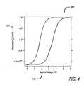
- FIG. 4shows a polarization hysteresis loop 400 measured on the amorphous ferroelectric material 202 of FIG. 3 .
- an applied voltage 402can be used to store information through a polarization 404 on the amorphous ferroelectric material, which can later be read.
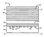
- an exemplary capacitor-based amorphous ferroelectric memory device 502is formed.
- this capacitor-based amorphous ferroelectric devicecomprises substrate 104 and amorphous ferroelectric material 202 , both of FIG. 2 . It also comprises a cross-bar structure 504 capable of selectively writing and reading the regions 306 residing between intersection areas of cross-bars 506 of the cross-bar structure.
- This devicecan be integrally formed with a temperature-sensitive device or structure, such as an IC.
Landscapes
- Engineering & Computer Science (AREA)
- Computer Hardware Design (AREA)
- Semiconductor Memories (AREA)
- Semiconductor Integrated Circuits (AREA)
Abstract
Description
- This invention relates to ferroelectric memory devices and methods of forming the same.
- Ferroelectric memory devices use ferroelectric materials to store information. These materials can store information by retaining a polarization state after exposure to an electric field.
- Some of these devices have a sheet of ferroelectric material layered over a conductive layer. A writing device, such as a plate or point, can be used to expose regions of the ferroelectric sheet to an electric field. The plate or point acts to create an electric field in the region by placing a charge over the region opposite the conductive layer. This region is polarized, the polarization state is then retained after the electric field dissipates.
- The surface charge of the region can later be read by a reading device. The reading device moves another plate or point over the ferroelectric sheet, thereby reading the polarization state of the regions.
- Many of these ferroelectric memory devices use polycrystalline ferroelectric materials to store information. These polycrystalline materials have a grain structure that can make reading their polarization state difficult. This is especially true when reading small regions of the polycrystalline materials because each small region often has a small number of grains. For a region having few grains, the noise from the grain structure interferes with accurate measurement of the region's polarization state.
- Also, many ferroelectric memory devices are physically integrated with integrated circuits (ICs). Polycrystalline ferroelectric materials are often fabricated at fairly high temperatures, which can cause problems with neighboring ICs.
- Others of these ferroelectric memory devices have single-crystal ferroelectric materials. These single-crystal materials are less likely to have problems associated with noise, but have other significant problems. First, fabricating single-crystal ferroelectric materials is relatively expensive. Second, fabricating them is often performed at high temperatures. These high temperatures can cause significant problems with neighboring ICs. If formed first and then added to an IC, the single crystals may be placed into the IC but this is difficult and expensive, especially if they are small.
FIG. 1 includes a cross-section of a substrate over which an amorphous ferroelectric material precursor is formed.FIG. 2 includes the cross-section of the substrate ofFIG. 1 at a processing step subsequent to that shown inFIG. 1 .FIG. 3 includes the viewFIG. 2 and a charged object for inducing an electric field over a region of an amorphous ferroelectric material.FIG. 4 shows an exemplary polarization hysteresis loop measured on an amorphous ferroelectric material.FIG. 5 includes a top-plan and side-sectional views of a cross-bar memory device having an amorphous ferroelectric material.- The same numbers are used throughout the disclosure and figures to reference like components and features.
- The embodiments described below employ an amorphous ferroelectric material in a memory device. One of these amorphous ferroelectric devices enables its polarization state to be read with low noise. By so doing, large amounts of information can be stored in a very small amount of ferroelectric material.
- Also, processes for forming amorphous ferroelectric memory devices are described, which, in some instances, use relatively low-temperature processing. By not relying on higher-temperature processing, amorphous ferroelectric memory devices can be integrally formed with temperature-sensitive devices and structures. One of these processes also enables formation of amorphous ferroelectric materials on or with a temperature-sensitive device using alignment-independent processing steps.
- Referring initially to
FIG. 1 , an amorphousferroelectric precursor 102 is formed over asubstrate 104. The amorphous ferroelectric precursor can comprise a ferroelectric compound or its constituent parts and other materials. In the illustrated embodiment, the amorphous ferroelectric precursor comprises lead, zirconium, titanium, and various organic compounds in a Sol-Gel. - The
precursor 102 can be formed oversubstrate 104 using a alignment-independent and/or low-temperature technique. In the illustrated embodiment, the precursor is spun on the substrate at about 25° C. In other embodiments, the precursor is formed using chemical vapor deposition, physical vapor deposition, or another suitable technique. - Referring to
FIG. 2 , an amorphousferroelectric material 202 is formed oversubstrate 104. The amorphous ferroelectric material can be formed as a layer, though other structures can also be used. In one embodiment, the amorphous ferroelectric material comprises lead-zirconium-titanate (Pb(Zr0.5Ti0.5)O3) or other suitable ferroelectrics. - The amorphous
ferroelectric material 202 can be formed using an alignment-independent and/or low-temperature technique. In the illustrated embodiment, theprecursor 102 is heated to about 350° C. This removes most of the organic materials in the Sol Gel and forms a layer of lead-zirconium-titanate. While not shown, the precursor can be disposed within or around a temperature-sensitive device or structure, such as an IC. Thus, the illustrated process enables formation of a ferroelectric material with a temperature-sensitive device or structure capable of withstanding temperatures of about 350° C. - In another embodiment, the amorphous ferroelectric material is formed without first forming the precursor. The amorphous
ferroelectric material 202 can be formed first and then placed over thesubstrate 104 using a suitable alignment-dependent technique, such as a robot capable of accurate placement. The amorphous ferroelectric material can also be formed by physically depositing a vaporized ferroelectric material at low temperature, such as 25° C. to 150° C. This low temperature enables the material to be formed as an amorphous structure. It can also enable formation of the amorphous ferroelectric material within or around a temperature-sensitive device or structure, such as an IC capable of withstanding about 150° C. This alignment-independent technique for forming the amorphous ferroelectric material can be less costly by not requiring a robot or similar device. It may also permit very small sizes or highly accurate placement that is not practicable with an alignment-dependent technique. - Referring to
FIG. 3 , an exemplary probe-based amorphousferroelectric memory device 302 is formed. In the illustrated embodiment, this probe-based amorphous ferroelectric device comprisessubstrate 104 and amorphousferroelectric material 202, both ofFIG. 2 . When a charged object304 (here a small plate), is oriented over the amorphous ferroelectric material, a change in the local polarization state is induced in aregion 306 between the object and the substrate. The charged object can create one or many millions (even trillions) of charged regions, depending on the object's size and the amorphous ferroelectric material's area. The polarized (“poled”) regions can later be read using atomic force microscopy techniques, by scanning the amorphous ferroelectric material's surface potential or capacitance, or other suitable techniques. The amorphous structure of the amorphousferroelectric material 202 can permit a reading device to read the material's polarization state with less interference from noise than often permitted with a polycrystalline structure. By so doing, the size ofregions 306 can be made very small to increase the information density of the memory device. - In the illustrated embodiment,
substrate 104 comprises device-grade silicon and the amorphousferroelectric material 202 is layered to a thickness of about 250 nanometers of lead-zirconium-titanate. The writeability and readability of the illustrated amorphous ferroelectric memory device has been experimentally shown. FIG. 4 shows apolarization hysteresis loop 400 measured on the amorphousferroelectric material 202 ofFIG. 3 . As this figure shows, an appliedvoltage 402 can be used to store information through apolarization 404 on the amorphous ferroelectric material, which can later be read.- Referring to
FIG. 5 , an exemplary capacitor-based amorphousferroelectric memory device 502 is formed. In the illustrated embodiment, shown in a top-plan and cross-sectional view along A-A′, this capacitor-based amorphous ferroelectric device comprisessubstrate 104 and amorphousferroelectric material 202, both ofFIG. 2 . It also comprises across-bar structure 504 capable of selectively writing and reading theregions 306 residing between intersection areas ofcross-bars 506 of the cross-bar structure. This device can be integrally formed with a temperature-sensitive device or structure, such as an IC. - Although the invention is described in language specific to structural features and methodological steps, it is to be understood that the invention defined in the appended claims is not necessarily limited to the specific features or steps described. Rather, the specific features and steps disclosed represent exemplary forms of implementing the claimed invention.
Claims (23)
Priority Applications (1)
| Application Number | Priority Date | Filing Date | Title |
|---|---|---|---|
| US12/217,657US7713754B2 (en) | 2004-09-30 | 2008-07-07 | Method of forming an amorphous ferroelectric memory device |
Applications Claiming Priority (2)
| Application Number | Priority Date | Filing Date | Title |
|---|---|---|---|
| US95569504A | 2004-09-30 | 2004-09-30 | |
| US12/217,657US7713754B2 (en) | 2004-09-30 | 2008-07-07 | Method of forming an amorphous ferroelectric memory device |
Related Parent Applications (1)
| Application Number | Title | Priority Date | Filing Date |
|---|---|---|---|
| US95569504ADivision | 2004-09-30 | 2004-09-30 |
Publications (2)
| Publication Number | Publication Date |
|---|---|
| US20090047747A1true US20090047747A1 (en) | 2009-02-19 |
| US7713754B2 US7713754B2 (en) | 2010-05-11 |
Family
ID=40363283
Family Applications (1)
| Application Number | Title | Priority Date | Filing Date |
|---|---|---|---|
| US12/217,657Expired - LifetimeUS7713754B2 (en) | 2004-09-30 | 2008-07-07 | Method of forming an amorphous ferroelectric memory device |
Country Status (1)
| Country | Link |
|---|---|
| US (1) | US7713754B2 (en) |
Citations (7)
| Publication number | Priority date | Publication date | Assignee | Title |
|---|---|---|---|---|
| US5342648A (en)* | 1991-05-01 | 1994-08-30 | The Regents Of The Universty Of California | Method for forming amorphous ferroelectric materials |
| US5728603A (en)* | 1994-11-28 | 1998-03-17 | Northern Telecom Limited | Method of forming a crystalline ferroelectric dielectric material for an integrated circuit |
| US5854499A (en)* | 1994-07-12 | 1998-12-29 | Texas Instruments Incorporated | Ferroelectric film capacitor with intergranular insulation |
| US5886867A (en)* | 1995-03-21 | 1999-03-23 | Northern Telecom Limited | Ferroelectric dielectric for integrated circuit applications at microwave frequencies |
| US6258608B1 (en)* | 1999-01-20 | 2001-07-10 | Samsung Electronics Co., Ltd. | Method for forming a crystalline perovskite ferroelectric material in a semiconductor device |
| US6309895B1 (en)* | 1998-10-27 | 2001-10-30 | Precision Instrument Development Center, National Science Council | Method for fabricating capacitor containing amorphous and polycrystalline ferroelectric films and method for forming amorphous ferroelectric film |
| US6475813B1 (en)* | 2001-08-13 | 2002-11-05 | Sharp Laboratories Of America, Inc. | MOCVD and annealing processes for C-axis oriented ferroelectric thin films |
- 2008
- 2008-07-07USUS12/217,657patent/US7713754B2/ennot_activeExpired - Lifetime
Patent Citations (8)
| Publication number | Priority date | Publication date | Assignee | Title |
|---|---|---|---|---|
| US5342648A (en)* | 1991-05-01 | 1994-08-30 | The Regents Of The Universty Of California | Method for forming amorphous ferroelectric materials |
| US5854499A (en)* | 1994-07-12 | 1998-12-29 | Texas Instruments Incorporated | Ferroelectric film capacitor with intergranular insulation |
| US5728603A (en)* | 1994-11-28 | 1998-03-17 | Northern Telecom Limited | Method of forming a crystalline ferroelectric dielectric material for an integrated circuit |
| US5886867A (en)* | 1995-03-21 | 1999-03-23 | Northern Telecom Limited | Ferroelectric dielectric for integrated circuit applications at microwave frequencies |
| US6077715A (en)* | 1995-03-21 | 2000-06-20 | Nortel Networks Corporation | Method for forming ferroelectric dielectric for integrated circuit applications at microwave frequencies |
| US6309895B1 (en)* | 1998-10-27 | 2001-10-30 | Precision Instrument Development Center, National Science Council | Method for fabricating capacitor containing amorphous and polycrystalline ferroelectric films and method for forming amorphous ferroelectric film |
| US6258608B1 (en)* | 1999-01-20 | 2001-07-10 | Samsung Electronics Co., Ltd. | Method for forming a crystalline perovskite ferroelectric material in a semiconductor device |
| US6475813B1 (en)* | 2001-08-13 | 2002-11-05 | Sharp Laboratories Of America, Inc. | MOCVD and annealing processes for C-axis oriented ferroelectric thin films |
Also Published As
| Publication number | Publication date |
|---|---|
| US7713754B2 (en) | 2010-05-11 |
Similar Documents
| Publication | Publication Date | Title |
|---|---|---|
| Auciello et al. | The physics of ferroelectric memories | |
| Ganpule et al. | Domain nucleation and relaxation kinetics in ferroelectric thin films | |
| Mueller et al. | Reliability Characteristics of Ferroelectric $\hbox {Si: HfO} _ {2} $ Thin Films for Memory Applications | |
| Ghoneim et al. | Thin PZT‐based ferroelectric capacitors on flexible silicon for nonvolatile memory applications | |
| Takahashi et al. | Thirty-day-long data retention in ferroelectric-gate field-effect transistors with HfO2 buffer layers | |
| US5434742A (en) | Capacitor for semiconductor integrated circuit and method of manufacturing the same | |
| Kim et al. | First-order reversal curve probing of spatially resolved polarization switching dynamics in ferroelectric nanocapacitors | |
| Chen et al. | Nonvolatile data storage using mechanical force-induced polarization switching in ferroelectric polymer | |
| EP0940856B1 (en) | Ferroelectric memory element and method of producing the same | |
| WO1998039800A1 (en) | Strontium bismuth niobate tantalate ferroelectric thin film | |
| Balke et al. | Manipulating ferroelectrics through changes in surface and interface properties | |
| JP2002535832A (en) | Ferroelectric device with capping layer and method of making same | |
| Huang et al. | Epitaxial PbZrxTi1− xO3 ferroelectric bilayers with giant electromechanical properties | |
| US6660536B2 (en) | Method of making ferroelectric material utilizing anneal in an electrical field | |
| Tayebi et al. | Tuning the built-in electric field in ferroelectric Pb (Zr0. 2Ti0. 8) O3 films for long-term stability of single-digit nanometer inverted domains | |
| Lederer et al. | Impact of the interface layer on the cycling behaviour and retention of ferroelectric hafnium oxide | |
| US20090047747A1 (en) | Method of forming an amorphous ferroelectric memory device | |
| Nagasawa et al. | Imprint model based on thermionic electron emission under local fields in ferroelectric thin films | |
| CN115621259A (en) | A method for improving the performance of ferroelectric devices by using hard electrodes under low temperature annealing conditions | |
| US20230326747A1 (en) | Method for producing a ferroelectric layer or an antiferroelectric layer | |
| Jiang et al. | A fabrication and measurement method for a flexible ferroelectric element based on van der Waals heteroepitaxy | |
| Lee et al. | The problems originating from the grain boundaries in dielectric storage capacitors | |
| Pane et al. | Effect of geometry upon the performance of a thin film ferroelectric capacitor | |
| US20080142859A1 (en) | Methods of forming ferroelectric media with patterned nano structures for data storage devices | |
| CN100536024C (en) | Data recording medium including ferroelectric layer and method of manufacturing the same |
Legal Events
| Date | Code | Title | Description |
|---|---|---|---|
| STCF | Information on status: patent grant | Free format text:PATENTED CASE | |
| AS | Assignment | Owner name:SAMSUNG ELECTRONICS CO., LTD., KOREA, REPUBLIC OF Free format text:ASSIGNMENT OF ASSIGNORS INTEREST;ASSIGNORS:HEWLETT-PACKARD DEVELOPMENT COMPANY, L.P.;HEWLETT-PACKARD COMPANY;REEL/FRAME:025920/0001 Effective date:20100421 | |
| AS | Assignment | Owner name:SAMSUNG ELECTRONICS CO., LTD., KOREA, REPUBLIC OF Free format text:ASSIGNMENT OF ASSIGNORS INTEREST;ASSIGNORS:HEWLETT-PACKARD DEVELOPMENT COMPANY, L.P.;HEWLETT-PACKARD COMPANY;REEL/FRAME:026311/0424 Effective date:20100421 | |
| FPAY | Fee payment | Year of fee payment:4 | |
| MAFP | Maintenance fee payment | Free format text:PAYMENT OF MAINTENANCE FEE, 8TH YEAR, LARGE ENTITY (ORIGINAL EVENT CODE: M1552) Year of fee payment:8 | |
| MAFP | Maintenance fee payment | Free format text:PAYMENT OF MAINTENANCE FEE, 12TH YEAR, LARGE ENTITY (ORIGINAL EVENT CODE: M1553); ENTITY STATUS OF PATENT OWNER: LARGE ENTITY Year of fee payment:12 |