US20090039523A1 - Packaged integrated circuit devices with through-body conductive vias, and methods of making same - Google Patents
Packaged integrated circuit devices with through-body conductive vias, and methods of making sameDownload PDFInfo
- Publication number
- US20090039523A1 US20090039523A1US11/834,765US83476507AUS2009039523A1US 20090039523 A1US20090039523 A1US 20090039523A1US 83476507 AUS83476507 AUS 83476507AUS 2009039523 A1US2009039523 A1US 2009039523A1
- Authority
- US
- United States
- Prior art keywords
- die
- embedded die
- individual embedded
- conductive
- integrated circuit
- Prior art date
- Legal status (The legal status is an assumption and is not a legal conclusion. Google has not performed a legal analysis and makes no representation as to the accuracy of the status listed.)
- Granted
Links
Images


Classifications
- H—ELECTRICITY
- H01—ELECTRIC ELEMENTS
- H01L—SEMICONDUCTOR DEVICES NOT COVERED BY CLASS H10
- H01L25/00—Assemblies consisting of a plurality of semiconductor or other solid state devices
- H01L25/03—Assemblies consisting of a plurality of semiconductor or other solid state devices all the devices being of a type provided for in a single subclass of subclasses H10B, H10D, H10F, H10H, H10K or H10N, e.g. assemblies of rectifier diodes
- H01L25/04—Assemblies consisting of a plurality of semiconductor or other solid state devices all the devices being of a type provided for in a single subclass of subclasses H10B, H10D, H10F, H10H, H10K or H10N, e.g. assemblies of rectifier diodes the devices not having separate containers
- H01L25/07—Assemblies consisting of a plurality of semiconductor or other solid state devices all the devices being of a type provided for in a single subclass of subclasses H10B, H10D, H10F, H10H, H10K or H10N, e.g. assemblies of rectifier diodes the devices not having separate containers the devices being of a type provided for in group subclass H10D
- H01L25/071—Assemblies consisting of a plurality of semiconductor or other solid state devices all the devices being of a type provided for in a single subclass of subclasses H10B, H10D, H10F, H10H, H10K or H10N, e.g. assemblies of rectifier diodes the devices not having separate containers the devices being of a type provided for in group subclass H10D the devices being arranged next and on each other, i.e. mixed assemblies
- H—ELECTRICITY
- H01—ELECTRIC ELEMENTS
- H01L—SEMICONDUCTOR DEVICES NOT COVERED BY CLASS H10
- H01L21/00—Processes or apparatus adapted for the manufacture or treatment of semiconductor or solid state devices or of parts thereof
- H01L21/02—Manufacture or treatment of semiconductor devices or of parts thereof
- H01L21/04—Manufacture or treatment of semiconductor devices or of parts thereof the devices having potential barriers, e.g. a PN junction, depletion layer or carrier concentration layer
- H01L21/50—Assembly of semiconductor devices using processes or apparatus not provided for in a single one of the groups H01L21/18 - H01L21/326 or H10D48/04 - H10D48/07 e.g. sealing of a cap to a base of a container
- H01L21/56—Encapsulations, e.g. encapsulation layers, coatings
- H01L21/561—Batch processing
- H—ELECTRICITY
- H01—ELECTRIC ELEMENTS
- H01L—SEMICONDUCTOR DEVICES NOT COVERED BY CLASS H10
- H01L21/00—Processes or apparatus adapted for the manufacture or treatment of semiconductor or solid state devices or of parts thereof
- H01L21/02—Manufacture or treatment of semiconductor devices or of parts thereof
- H01L21/04—Manufacture or treatment of semiconductor devices or of parts thereof the devices having potential barriers, e.g. a PN junction, depletion layer or carrier concentration layer
- H01L21/50—Assembly of semiconductor devices using processes or apparatus not provided for in a single one of the groups H01L21/18 - H01L21/326 or H10D48/04 - H10D48/07 e.g. sealing of a cap to a base of a container
- H01L21/56—Encapsulations, e.g. encapsulation layers, coatings
- H01L21/568—Temporary substrate used as encapsulation process aid
- H—ELECTRICITY
- H01—ELECTRIC ELEMENTS
- H01L—SEMICONDUCTOR DEVICES NOT COVERED BY CLASS H10
- H01L21/00—Processes or apparatus adapted for the manufacture or treatment of semiconductor or solid state devices or of parts thereof
- H01L21/70—Manufacture or treatment of devices consisting of a plurality of solid state components formed in or on a common substrate or of parts thereof; Manufacture of integrated circuit devices or of parts thereof
- H01L21/71—Manufacture of specific parts of devices defined in group H01L21/70
- H01L21/768—Applying interconnections to be used for carrying current between separate components within a device comprising conductors and dielectrics
- H01L21/76838—Applying interconnections to be used for carrying current between separate components within a device comprising conductors and dielectrics characterised by the formation and the after-treatment of the conductors
- H01L21/76877—Filling of holes, grooves or trenches, e.g. vias, with conductive material
- H—ELECTRICITY
- H01—ELECTRIC ELEMENTS
- H01L—SEMICONDUCTOR DEVICES NOT COVERED BY CLASS H10
- H01L23/00—Details of semiconductor or other solid state devices
- H01L23/28—Encapsulations, e.g. encapsulating layers, coatings, e.g. for protection
- H01L23/31—Encapsulations, e.g. encapsulating layers, coatings, e.g. for protection characterised by the arrangement or shape
- H01L23/3107—Encapsulations, e.g. encapsulating layers, coatings, e.g. for protection characterised by the arrangement or shape the device being completely enclosed
- H01L23/3114—Encapsulations, e.g. encapsulating layers, coatings, e.g. for protection characterised by the arrangement or shape the device being completely enclosed the device being a chip scale package, e.g. CSP
- H—ELECTRICITY
- H01—ELECTRIC ELEMENTS
- H01L—SEMICONDUCTOR DEVICES NOT COVERED BY CLASS H10
- H01L23/00—Details of semiconductor or other solid state devices
- H01L23/28—Encapsulations, e.g. encapsulating layers, coatings, e.g. for protection
- H01L23/31—Encapsulations, e.g. encapsulating layers, coatings, e.g. for protection characterised by the arrangement or shape
- H01L23/3107—Encapsulations, e.g. encapsulating layers, coatings, e.g. for protection characterised by the arrangement or shape the device being completely enclosed
- H01L23/3142—Sealing arrangements between parts, e.g. adhesion promotors
- H—ELECTRICITY
- H01—ELECTRIC ELEMENTS
- H01L—SEMICONDUCTOR DEVICES NOT COVERED BY CLASS H10
- H01L23/00—Details of semiconductor or other solid state devices
- H01L23/48—Arrangements for conducting electric current to or from the solid state body in operation, e.g. leads, terminal arrangements ; Selection of materials therefor
- H01L23/481—Internal lead connections, e.g. via connections, feedthrough structures
- H—ELECTRICITY
- H01—ELECTRIC ELEMENTS
- H01L—SEMICONDUCTOR DEVICES NOT COVERED BY CLASS H10
- H01L23/00—Details of semiconductor or other solid state devices
- H01L23/52—Arrangements for conducting electric current within the device in operation from one component to another, i.e. interconnections, e.g. wires, lead frames
- H01L23/538—Arrangements for conducting electric current within the device in operation from one component to another, i.e. interconnections, e.g. wires, lead frames the interconnection structure between a plurality of semiconductor chips being formed on, or in, insulating substrates
- H01L23/5389—Arrangements for conducting electric current within the device in operation from one component to another, i.e. interconnections, e.g. wires, lead frames the interconnection structure between a plurality of semiconductor chips being formed on, or in, insulating substrates the chips being integrally enclosed by the interconnect and support structures
- H—ELECTRICITY
- H01—ELECTRIC ELEMENTS
- H01L—SEMICONDUCTOR DEVICES NOT COVERED BY CLASS H10
- H01L24/00—Arrangements for connecting or disconnecting semiconductor or solid-state bodies; Methods or apparatus related thereto
- H01L24/01—Means for bonding being attached to, or being formed on, the surface to be connected, e.g. chip-to-package, die-attach, "first-level" interconnects; Manufacturing methods related thereto
- H01L24/18—High density interconnect [HDI] connectors; Manufacturing methods related thereto
- H01L24/19—Manufacturing methods of high density interconnect preforms
- H—ELECTRICITY
- H01—ELECTRIC ELEMENTS
- H01L—SEMICONDUCTOR DEVICES NOT COVERED BY CLASS H10
- H01L24/00—Arrangements for connecting or disconnecting semiconductor or solid-state bodies; Methods or apparatus related thereto
- H01L24/01—Means for bonding being attached to, or being formed on, the surface to be connected, e.g. chip-to-package, die-attach, "first-level" interconnects; Manufacturing methods related thereto
- H01L24/26—Layer connectors, e.g. plate connectors, solder or adhesive layers; Manufacturing methods related thereto
- H01L24/27—Manufacturing methods
- H—ELECTRICITY
- H01—ELECTRIC ELEMENTS
- H01L—SEMICONDUCTOR DEVICES NOT COVERED BY CLASS H10
- H01L24/00—Arrangements for connecting or disconnecting semiconductor or solid-state bodies; Methods or apparatus related thereto
- H01L24/01—Means for bonding being attached to, or being formed on, the surface to be connected, e.g. chip-to-package, die-attach, "first-level" interconnects; Manufacturing methods related thereto
- H01L24/26—Layer connectors, e.g. plate connectors, solder or adhesive layers; Manufacturing methods related thereto
- H01L24/31—Structure, shape, material or disposition of the layer connectors after the connecting process
- H01L24/32—Structure, shape, material or disposition of the layer connectors after the connecting process of an individual layer connector
- H—ELECTRICITY
- H01—ELECTRIC ELEMENTS
- H01L—SEMICONDUCTOR DEVICES NOT COVERED BY CLASS H10
- H01L24/00—Arrangements for connecting or disconnecting semiconductor or solid-state bodies; Methods or apparatus related thereto
- H01L24/80—Methods for connecting semiconductor or other solid state bodies using means for bonding being attached to, or being formed on, the surface to be connected
- H01L24/83—Methods for connecting semiconductor or other solid state bodies using means for bonding being attached to, or being formed on, the surface to be connected using a layer connector
- H—ELECTRICITY
- H01—ELECTRIC ELEMENTS
- H01L—SEMICONDUCTOR DEVICES NOT COVERED BY CLASS H10
- H01L24/00—Arrangements for connecting or disconnecting semiconductor or solid-state bodies; Methods or apparatus related thereto
- H01L24/93—Batch processes
- H01L24/95—Batch processes at chip-level, i.e. with connecting carried out on a plurality of singulated devices, i.e. on diced chips
- H01L24/96—Batch processes at chip-level, i.e. with connecting carried out on a plurality of singulated devices, i.e. on diced chips the devices being encapsulated in a common layer, e.g. neo-wafer or pseudo-wafer, said common layer being separable into individual assemblies after connecting
- H—ELECTRICITY
- H01—ELECTRIC ELEMENTS
- H01L—SEMICONDUCTOR DEVICES NOT COVERED BY CLASS H10
- H01L24/00—Arrangements for connecting or disconnecting semiconductor or solid-state bodies; Methods or apparatus related thereto
- H01L24/93—Batch processes
- H01L24/95—Batch processes at chip-level, i.e. with connecting carried out on a plurality of singulated devices, i.e. on diced chips
- H01L24/97—Batch processes at chip-level, i.e. with connecting carried out on a plurality of singulated devices, i.e. on diced chips the devices being connected to a common substrate, e.g. interposer, said common substrate being separable into individual assemblies after connecting
- H—ELECTRICITY
- H01—ELECTRIC ELEMENTS
- H01L—SEMICONDUCTOR DEVICES NOT COVERED BY CLASS H10
- H01L25/00—Assemblies consisting of a plurality of semiconductor or other solid state devices
- H01L25/03—Assemblies consisting of a plurality of semiconductor or other solid state devices all the devices being of a type provided for in a single subclass of subclasses H10B, H10D, H10F, H10H, H10K or H10N, e.g. assemblies of rectifier diodes
- H01L25/10—Assemblies consisting of a plurality of semiconductor or other solid state devices all the devices being of a type provided for in a single subclass of subclasses H10B, H10D, H10F, H10H, H10K or H10N, e.g. assemblies of rectifier diodes the devices having separate containers
- H01L25/105—Assemblies consisting of a plurality of semiconductor or other solid state devices all the devices being of a type provided for in a single subclass of subclasses H10B, H10D, H10F, H10H, H10K or H10N, e.g. assemblies of rectifier diodes the devices having separate containers the devices being integrated devices of class H10
- H—ELECTRICITY
- H01—ELECTRIC ELEMENTS
- H01L—SEMICONDUCTOR DEVICES NOT COVERED BY CLASS H10
- H01L25/00—Assemblies consisting of a plurality of semiconductor or other solid state devices
- H01L25/50—Multistep manufacturing processes of assemblies consisting of devices, the devices being individual devices of subclass H10D or integrated devices of class H10
- H—ELECTRICITY
- H10—SEMICONDUCTOR DEVICES; ELECTRIC SOLID-STATE DEVICES NOT OTHERWISE PROVIDED FOR
- H10D—INORGANIC ELECTRIC SEMICONDUCTOR DEVICES
- H10D84/00—Integrated devices formed in or on semiconductor substrates that comprise only semiconducting layers, e.g. on Si wafers or on GaAs-on-Si wafers
- H10D84/01—Manufacture or treatment
- H—ELECTRICITY
- H01—ELECTRIC ELEMENTS
- H01L—SEMICONDUCTOR DEVICES NOT COVERED BY CLASS H10
- H01L2221/00—Processes or apparatus adapted for the manufacture or treatment of semiconductor or solid state devices or of parts thereof covered by H01L21/00
- H01L2221/67—Apparatus for handling semiconductor or electric solid state devices during manufacture or treatment thereof; Apparatus for handling wafers during manufacture or treatment of semiconductor or electric solid state devices or components; Apparatus not specifically provided for elsewhere
- H01L2221/683—Apparatus for handling semiconductor or electric solid state devices during manufacture or treatment thereof; Apparatus for handling wafers during manufacture or treatment of semiconductor or electric solid state devices or components; Apparatus not specifically provided for elsewhere for supporting or gripping
- H01L2221/68304—Apparatus for handling semiconductor or electric solid state devices during manufacture or treatment thereof; Apparatus for handling wafers during manufacture or treatment of semiconductor or electric solid state devices or components; Apparatus not specifically provided for elsewhere for supporting or gripping using temporarily an auxiliary support
- H01L2221/68359—Apparatus for handling semiconductor or electric solid state devices during manufacture or treatment thereof; Apparatus for handling wafers during manufacture or treatment of semiconductor or electric solid state devices or components; Apparatus not specifically provided for elsewhere for supporting or gripping using temporarily an auxiliary support used as a support during manufacture of interconnect decals or build up layers
- H—ELECTRICITY
- H01—ELECTRIC ELEMENTS
- H01L—SEMICONDUCTOR DEVICES NOT COVERED BY CLASS H10
- H01L2224/00—Indexing scheme for arrangements for connecting or disconnecting semiconductor or solid-state bodies and methods related thereto as covered by H01L24/00
- H01L2224/01—Means for bonding being attached to, or being formed on, the surface to be connected, e.g. chip-to-package, die-attach, "first-level" interconnects; Manufacturing methods related thereto
- H01L2224/02—Bonding areas; Manufacturing methods related thereto
- H01L2224/04—Structure, shape, material or disposition of the bonding areas prior to the connecting process
- H01L2224/04105—Bonding areas formed on an encapsulation of the semiconductor or solid-state body, e.g. bonding areas on chip-scale packages
- H—ELECTRICITY
- H01—ELECTRIC ELEMENTS
- H01L—SEMICONDUCTOR DEVICES NOT COVERED BY CLASS H10
- H01L2224/00—Indexing scheme for arrangements for connecting or disconnecting semiconductor or solid-state bodies and methods related thereto as covered by H01L24/00
- H01L2224/01—Means for bonding being attached to, or being formed on, the surface to be connected, e.g. chip-to-package, die-attach, "first-level" interconnects; Manufacturing methods related thereto
- H01L2224/10—Bump connectors; Manufacturing methods related thereto
- H01L2224/12—Structure, shape, material or disposition of the bump connectors prior to the connecting process
- H01L2224/12105—Bump connectors formed on an encapsulation of the semiconductor or solid-state body, e.g. bumps on chip-scale packages
- H—ELECTRICITY
- H01—ELECTRIC ELEMENTS
- H01L—SEMICONDUCTOR DEVICES NOT COVERED BY CLASS H10
- H01L2224/00—Indexing scheme for arrangements for connecting or disconnecting semiconductor or solid-state bodies and methods related thereto as covered by H01L24/00
- H01L2224/01—Means for bonding being attached to, or being formed on, the surface to be connected, e.g. chip-to-package, die-attach, "first-level" interconnects; Manufacturing methods related thereto
- H01L2224/18—High density interconnect [HDI] connectors; Manufacturing methods related thereto
- H01L2224/20—Structure, shape, material or disposition of high density interconnect preforms
- H—ELECTRICITY
- H01—ELECTRIC ELEMENTS
- H01L—SEMICONDUCTOR DEVICES NOT COVERED BY CLASS H10
- H01L2224/00—Indexing scheme for arrangements for connecting or disconnecting semiconductor or solid-state bodies and methods related thereto as covered by H01L24/00
- H01L2224/01—Means for bonding being attached to, or being formed on, the surface to be connected, e.g. chip-to-package, die-attach, "first-level" interconnects; Manufacturing methods related thereto
- H01L2224/26—Layer connectors, e.g. plate connectors, solder or adhesive layers; Manufacturing methods related thereto
- H01L2224/31—Structure, shape, material or disposition of the layer connectors after the connecting process
- H01L2224/32—Structure, shape, material or disposition of the layer connectors after the connecting process of an individual layer connector
- H01L2224/321—Disposition
- H01L2224/32135—Disposition the layer connector connecting between different semiconductor or solid-state bodies, i.e. chip-to-chip
- H01L2224/32145—Disposition the layer connector connecting between different semiconductor or solid-state bodies, i.e. chip-to-chip the bodies being stacked
- H—ELECTRICITY
- H01—ELECTRIC ELEMENTS
- H01L—SEMICONDUCTOR DEVICES NOT COVERED BY CLASS H10
- H01L2224/00—Indexing scheme for arrangements for connecting or disconnecting semiconductor or solid-state bodies and methods related thereto as covered by H01L24/00
- H01L2224/80—Methods for connecting semiconductor or other solid state bodies using means for bonding being attached to, or being formed on, the surface to be connected
- H01L2224/83—Methods for connecting semiconductor or other solid state bodies using means for bonding being attached to, or being formed on, the surface to be connected using a layer connector
- H01L2224/8319—Arrangement of the layer connectors prior to mounting
- H01L2224/83193—Arrangement of the layer connectors prior to mounting wherein the layer connectors are disposed on both the semiconductor or solid-state body and another item or body to be connected to the semiconductor or solid-state body
- H—ELECTRICITY
- H01—ELECTRIC ELEMENTS
- H01L—SEMICONDUCTOR DEVICES NOT COVERED BY CLASS H10
- H01L2224/00—Indexing scheme for arrangements for connecting or disconnecting semiconductor or solid-state bodies and methods related thereto as covered by H01L24/00
- H01L2224/80—Methods for connecting semiconductor or other solid state bodies using means for bonding being attached to, or being formed on, the surface to be connected
- H01L2224/83—Methods for connecting semiconductor or other solid state bodies using means for bonding being attached to, or being formed on, the surface to be connected using a layer connector
- H01L2224/838—Bonding techniques
- H—ELECTRICITY
- H01—ELECTRIC ELEMENTS
- H01L—SEMICONDUCTOR DEVICES NOT COVERED BY CLASS H10
- H01L2225/00—Details relating to assemblies covered by the group H01L25/00 but not provided for in its subgroups
- H01L2225/03—All the devices being of a type provided for in the same main group of the same subclass of class H10, e.g. assemblies of rectifier diodes
- H01L2225/04—All the devices being of a type provided for in the same main group of the same subclass of class H10, e.g. assemblies of rectifier diodes the devices not having separate containers
- H01L2225/065—All the devices being of a type provided for in the same main group of the same subclass of class H10
- H01L2225/06503—Stacked arrangements of devices
- H01L2225/06548—Conductive via connections through the substrate, container, or encapsulation
- H—ELECTRICITY
- H01—ELECTRIC ELEMENTS
- H01L—SEMICONDUCTOR DEVICES NOT COVERED BY CLASS H10
- H01L2225/00—Details relating to assemblies covered by the group H01L25/00 but not provided for in its subgroups
- H01L2225/03—All the devices being of a type provided for in the same main group of the same subclass of class H10, e.g. assemblies of rectifier diodes
- H01L2225/10—All the devices being of a type provided for in the same main group of the same subclass of class H10, e.g. assemblies of rectifier diodes the devices having separate containers
- H01L2225/1005—All the devices being of a type provided for in the same main group of the same subclass of class H10, e.g. assemblies of rectifier diodes the devices having separate containers the devices being integrated devices of class H10
- H01L2225/1011—All the devices being of a type provided for in the same main group of the same subclass of class H10, e.g. assemblies of rectifier diodes the devices having separate containers the devices being integrated devices of class H10 the containers being in a stacked arrangement
- H01L2225/1017—All the devices being of a type provided for in the same main group of the same subclass of class H10, e.g. assemblies of rectifier diodes the devices having separate containers the devices being integrated devices of class H10 the containers being in a stacked arrangement the lowermost container comprising a device support
- H01L2225/1035—All the devices being of a type provided for in the same main group of the same subclass of class H10, e.g. assemblies of rectifier diodes the devices having separate containers the devices being integrated devices of class H10 the containers being in a stacked arrangement the lowermost container comprising a device support the device being entirely enclosed by the support, e.g. high-density interconnect [HDI]
- H—ELECTRICITY
- H01—ELECTRIC ELEMENTS
- H01L—SEMICONDUCTOR DEVICES NOT COVERED BY CLASS H10
- H01L2225/00—Details relating to assemblies covered by the group H01L25/00 but not provided for in its subgroups
- H01L2225/03—All the devices being of a type provided for in the same main group of the same subclass of class H10, e.g. assemblies of rectifier diodes
- H01L2225/10—All the devices being of a type provided for in the same main group of the same subclass of class H10, e.g. assemblies of rectifier diodes the devices having separate containers
- H01L2225/1005—All the devices being of a type provided for in the same main group of the same subclass of class H10, e.g. assemblies of rectifier diodes the devices having separate containers the devices being integrated devices of class H10
- H01L2225/1011—All the devices being of a type provided for in the same main group of the same subclass of class H10, e.g. assemblies of rectifier diodes the devices having separate containers the devices being integrated devices of class H10 the containers being in a stacked arrangement
- H01L2225/1047—Details of electrical connections between containers
- H01L2225/1058—Bump or bump-like electrical connections, e.g. balls, pillars, posts
- H—ELECTRICITY
- H01—ELECTRIC ELEMENTS
- H01L—SEMICONDUCTOR DEVICES NOT COVERED BY CLASS H10
- H01L2924/00—Indexing scheme for arrangements or methods for connecting or disconnecting semiconductor or solid-state bodies as covered by H01L24/00
- H01L2924/01—Chemical elements
- H01L2924/01005—Boron [B]
- H—ELECTRICITY
- H01—ELECTRIC ELEMENTS
- H01L—SEMICONDUCTOR DEVICES NOT COVERED BY CLASS H10
- H01L2924/00—Indexing scheme for arrangements or methods for connecting or disconnecting semiconductor or solid-state bodies as covered by H01L24/00
- H01L2924/01—Chemical elements
- H01L2924/01006—Carbon [C]
- H—ELECTRICITY
- H01—ELECTRIC ELEMENTS
- H01L—SEMICONDUCTOR DEVICES NOT COVERED BY CLASS H10
- H01L2924/00—Indexing scheme for arrangements or methods for connecting or disconnecting semiconductor or solid-state bodies as covered by H01L24/00
- H01L2924/01—Chemical elements
- H01L2924/01013—Aluminum [Al]
- H—ELECTRICITY
- H01—ELECTRIC ELEMENTS
- H01L—SEMICONDUCTOR DEVICES NOT COVERED BY CLASS H10
- H01L2924/00—Indexing scheme for arrangements or methods for connecting or disconnecting semiconductor or solid-state bodies as covered by H01L24/00
- H01L2924/01—Chemical elements
- H01L2924/01029—Copper [Cu]
- H—ELECTRICITY
- H01—ELECTRIC ELEMENTS
- H01L—SEMICONDUCTOR DEVICES NOT COVERED BY CLASS H10
- H01L2924/00—Indexing scheme for arrangements or methods for connecting or disconnecting semiconductor or solid-state bodies as covered by H01L24/00
- H01L2924/01—Chemical elements
- H01L2924/01033—Arsenic [As]
- H—ELECTRICITY
- H01—ELECTRIC ELEMENTS
- H01L—SEMICONDUCTOR DEVICES NOT COVERED BY CLASS H10
- H01L2924/00—Indexing scheme for arrangements or methods for connecting or disconnecting semiconductor or solid-state bodies as covered by H01L24/00
- H01L2924/01—Chemical elements
- H01L2924/01047—Silver [Ag]
- H—ELECTRICITY
- H01—ELECTRIC ELEMENTS
- H01L—SEMICONDUCTOR DEVICES NOT COVERED BY CLASS H10
- H01L2924/00—Indexing scheme for arrangements or methods for connecting or disconnecting semiconductor or solid-state bodies as covered by H01L24/00
- H01L2924/01—Chemical elements
- H01L2924/01075—Rhenium [Re]
- H—ELECTRICITY
- H01—ELECTRIC ELEMENTS
- H01L—SEMICONDUCTOR DEVICES NOT COVERED BY CLASS H10
- H01L2924/00—Indexing scheme for arrangements or methods for connecting or disconnecting semiconductor or solid-state bodies as covered by H01L24/00
- H01L2924/01—Chemical elements
- H01L2924/01078—Platinum [Pt]
- H—ELECTRICITY
- H01—ELECTRIC ELEMENTS
- H01L—SEMICONDUCTOR DEVICES NOT COVERED BY CLASS H10
- H01L2924/00—Indexing scheme for arrangements or methods for connecting or disconnecting semiconductor or solid-state bodies as covered by H01L24/00
- H01L2924/01—Chemical elements
- H01L2924/01082—Lead [Pb]
- H—ELECTRICITY
- H01—ELECTRIC ELEMENTS
- H01L—SEMICONDUCTOR DEVICES NOT COVERED BY CLASS H10
- H01L2924/00—Indexing scheme for arrangements or methods for connecting or disconnecting semiconductor or solid-state bodies as covered by H01L24/00
- H01L2924/10—Details of semiconductor or other solid state devices to be connected
- H01L2924/102—Material of the semiconductor or solid state bodies
- H01L2924/1025—Semiconducting materials
- H01L2924/10251—Elemental semiconductors, i.e. Group IV
- H01L2924/10253—Silicon [Si]
- H—ELECTRICITY
- H01—ELECTRIC ELEMENTS
- H01L—SEMICONDUCTOR DEVICES NOT COVERED BY CLASS H10
- H01L2924/00—Indexing scheme for arrangements or methods for connecting or disconnecting semiconductor or solid-state bodies as covered by H01L24/00
- H01L2924/10—Details of semiconductor or other solid state devices to be connected
- H01L2924/11—Device type
- H01L2924/12—Passive devices, e.g. 2 terminal devices
- H01L2924/1204—Optical Diode
- H01L2924/12042—LASER
- H—ELECTRICITY
- H01—ELECTRIC ELEMENTS
- H01L—SEMICONDUCTOR DEVICES NOT COVERED BY CLASS H10
- H01L2924/00—Indexing scheme for arrangements or methods for connecting or disconnecting semiconductor or solid-state bodies as covered by H01L24/00
- H01L2924/10—Details of semiconductor or other solid state devices to be connected
- H01L2924/11—Device type
- H01L2924/14—Integrated circuits
- H—ELECTRICITY
- H01—ELECTRIC ELEMENTS
- H01L—SEMICONDUCTOR DEVICES NOT COVERED BY CLASS H10
- H01L2924/00—Indexing scheme for arrangements or methods for connecting or disconnecting semiconductor or solid-state bodies as covered by H01L24/00
- H01L2924/15—Details of package parts other than the semiconductor or other solid state devices to be connected
- H01L2924/181—Encapsulation
- H—ELECTRICITY
- H01—ELECTRIC ELEMENTS
- H01L—SEMICONDUCTOR DEVICES NOT COVERED BY CLASS H10
- H01L2924/00—Indexing scheme for arrangements or methods for connecting or disconnecting semiconductor or solid-state bodies as covered by H01L24/00
- H01L2924/19—Details of hybrid assemblies other than the semiconductor or other solid state devices to be connected
- H01L2924/1901—Structure
- H01L2924/1904—Component type
- H01L2924/19041—Component type being a capacitor
- H—ELECTRICITY
- H01—ELECTRIC ELEMENTS
- H01L—SEMICONDUCTOR DEVICES NOT COVERED BY CLASS H10
- H01L2924/00—Indexing scheme for arrangements or methods for connecting or disconnecting semiconductor or solid-state bodies as covered by H01L24/00
- H01L2924/19—Details of hybrid assemblies other than the semiconductor or other solid state devices to be connected
- H01L2924/1901—Structure
- H01L2924/1904—Component type
- H01L2924/19043—Component type being a resistor
Definitions
- This subject matter disclosed hereinis generally directed to the field of packaging integrated circuit devices, and, more particularly, to packaged integrated circuit devices with through-body conductive vias and various methods of making same.
- Integrated circuit technologyuses electrical devices, e.g., transistors, resistors, capacitors, etc., to formulate vast arrays of functional circuits.
- electrical devicese.g., transistors, resistors, capacitors, etc.
- the complexity of these circuitsrequires the use of an ever-increasing number of linked electrical devices so that the circuit may perform its intended function.
- the integrated circuitry dimensionsshrink.
- One challenge in the semiconductor industryis to develop improved methods for electrically connecting and packaging circuit devices which are fabricated on the same and/or on different wafers or chips. In general, it is desirable in the semiconductor industry to construct transistors which occupy less surface area on the silicon chip/die.
- DIPdual inline packages
- ZIPzig-zag inline packages
- SOJsmall outline J-bends
- TSOPthin small outline packages
- PLCCplastic leaded chip carriers
- SOICsmall outline integrated circuits
- PQFPplastic quad flat packs
- IDFinterdigitated leadframe
- packaged integrated circuit deviceshave been stacked on top of one another in an effort to conserve plot space.
- Prior art techniques for conductively coupling the stacked packaged integrated circuit devices to one anothertypically involved the formation of solder balls or wire bonds to establish this connection. What is desired is a new and improved technique for conductively coupling stacked packaged integrated circuit devices to one another.
- FIG. 1is a schematic depiction of an illustrative packaged integrated circuit die with a plurality of conductive through-body vias as described herein;
- FIG. 2is a schematic depiction of an illustrative packaged integrated circuit comprised of multiple die with a plurality of conductive through-body vias as described herein;
- FIG. 3is a schematic cross-sectional view of an illustrative stacked packaged device disclosed herein;
- FIG. 4is a schematic cross-sectional view of another illustrative stacked packaged device disclosed herein;
- FIG. 5is a schematic cross-sectional view of yet another illustrative stacked packaged device disclosed herein;
- FIGS. 6A-6Hschematically depict one illustrative method of forming the stacked packaged devices disclosed herein.
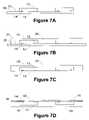
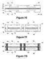
- FIGS. 7A-7Ischematically depict another illustrative method of forming the stacked packaged devices disclosed herein.
- FIG. 1depicts one illustrative embodiment of a packaged integrated circuit device 100 as described herein.
- the packaged integrated circuit device 100comprises an integrated circuit die 12 having a plurality of bond pads 14 , conductive wiring lines 16 (sometimes referred to as a redistribution layer (RDL)), and at least one conductive interconnection 18 (sometimes referred to as conductive vias) that extend through a body 20 of encapsulant material, e.g., mold compound material.
- the conductive via 18defines a conductive flow path through the thickness of the body 20 , i.e., between the front 13 and back 15 of the body 20 .
- the conductive via 18 and the integrated circuit die 12may be conductively coupled to one another using a variety of known techniques and structures.
- the conductive wiring line 16conductively couples the conductive via 18 to the integrated circuit die 12 .
- a plurality of schematically depicted solder balls 24are formed on the packaged integrated circuit device 100 in accordance with known processing techniques. The solder balls 24 , or other like connections, may be employed to conductively couple the packaged integrated circuit device 100 to another structure, e.g., a printed circuit board.
- the die 12is embedded in the body of encapsulant material 20 .
- the encapsulant materialwhen it is stated that one or more die 12 are embedded in a body of encapsulant material, it is to be understood that only portions of the body of the die 12 need to be positioned in the encapsulant material. It is not required that the encapsulant material surround all sides of the body of the die 12 , although that configuration may be employed if needed depending upon the particular application.
- FIG. 2depicts one illustrative embodiment of a packaged integrated circuit device 200 as described herein.
- the packaged integrated circuit device 200comprises a plurality of integrated circuit die 12 (two are shown) embedded in a single body 20 of encapsulant material, e.g., mold compound material.
- encapsulant materiale.g., mold compound material.
- each of the die 12have the same physical size.
- the die 12are not required to be the same physical size, nor do they have to perform the same function.
- FIG. 1depicts one illustrative embodiment of a packaged integrated circuit device 200 as described herein.
- the packaged integrated circuit device 200comprises a plurality of integrated circuit die 12 (two are shown) embedded in a single body 20 of encapsulant material, e.g., mold compound material.
- each of the die 12have the same physical size.
- the die 12are not required to be the same physical size, nor do they have to perform the same function.
- FIG. 1depicts one illustrative embodiment of
- the device 200has a plurality of bond pads 14 , conductive wiring lines 16 (sometimes referred to as a redistribution layer (RDL)), and at least one conductive interconnection 18 (sometimes referred to as conductive vias) that extend through the body 20 of encapsulant material.
- the device 200comprises a plurality of integrated circuit die 12 , it may be considered to be a multi-chip module (MCM).
- MCMmulti-chip module
- a plurality of schematically depicted solder balls 24are formed on the packaged integrated circuit device 200 in accordance with known processing techniques.
- the solder balls 24or other like connections, may be employed to conductively couple the packaged integrated circuit device 200 to another structure, e.g., a printed circuit board.
- each of the conductive vias 18 in FIG. 2extend through the thickness of the body 12 .
- the conductive coupling between and among the conductive vias 18 and the embedded integrated circuit die 12may b established using any of a variety of known techniques and structures.
- at least one of the conductive vias 18is conductively coupled to one of the integrated circuit die 12 by one or more wiring lines 16
- another of the conductive vias 18is conductively coupled to the other integrated circuit die 12 by one or more wiring lines 16 as well.
- the methods and techniques disclosed hereinmay be applied to virtually any type of integrated circuit device that may be formed on the die 12 . Additionally, the configuration and location of the schematically depicted bond pads 14 , the conductive wiring lines 16 , and the through-body conductive interconnections 18 may vary depending upon the particular application.
- FIGS. 3-5are schematic cross-sectional views of a plurality of stacked and packaged integrated circuit devices.
- the stacked package 300comprises a plurality of individual embedded die 10 A- 10 D.
- the illustrative example depicted in FIG. 3only four illustrative individual embedded die 10 A- 10 D are depicted.
- the structureneed only comprise at least one integrated circuit die with a portion of the die body positioned in the body 20 of encapsulant material.
- the number of individual embedded die 10 in the stacked package 300may vary depending upon the particular application, i.e., the number of individual embedded die 10 within such a stack 300 may be more or less than the illustrative four depicted in FIG. 3 .
- Each of the illustrative individual embedded die 10 A- 10 D in FIG. 3comprise an integrated circuit die 12 , a plurality of bond pads 14 , conductive wiring lines 16 (sometimes referred to as a redistribution layer (RDL)), a plurality of conductive interconnections 18 (sometimes referred to as conductive vias) that extend through the body 20 of encapsulated material.
- a plurality of conductive structures 22are provided between adjacent individual embedded die 10 to provide an electrically conductive path between the various embedded die 10 A- 10 D.
- a plurality of schematically depicted solder balls 24are formed on the packaged die 10 D in accordance with known processing techniques. The solder balls 24 , or other like connections, may be employed to conductively couple the stacked package 300 to another structure, e.g., a printed circuit board.
- the methods and techniques disclosed hereinmay be applied to virtually any type of integrated circuit device that may be formed on the die 12 and packaged in a stacked configuration. Additionally, the configuration and location of the schematically depicted bond pads 14 , conductive interconnections 18 and conductive structures 22 shown in FIG. 3 may vary depending upon the particular application. In the embodiment depicted in FIG. 3 , all of the packaged die are oriented with the front side 13 of the embedded die 10 facing a backside 15 of an adjacent embedded die 10 .
- FIG. 4depicts another illustrative embodiment of a stacked packaged device 400 . Similar to the embodiment shown in FIG. 3 , the embodiment in FIG. 4 comprises four illustrative individual embedded die 10 A- 10 D. In FIG. 4 , the individual embedded die 10 A- 10 D are assembled as groups 10 E and 10 F prior to assembling these groups into the structure shown in FIG. 4 .
- the first group 10 Ecomprises the individual embedded die 10 A and 10 B, while the second group 10 F comprises the individual embedded die 10 C and 10 D.
- a plurality of conductive interconnections or vias 32extend through the bodies 20 of the plurality of die 10 that comprise the first group 10 E, while a plurality of conductive interconnections or vias 34 extend through the bodies 20 of the plurality of the die 10 that comprise the second group 10 F.
- a plurality of conductive structures 22provide an electrically conductive path between the two groups 10 E and 10 F.
- the individual embedded die 10 within each groupmay be secured to one another using an adhesive material 28 .
- the backside 15 of adjacent embedded die 10are positioned facing one another.
- the number of groups, e.g., groups 10 E and 10 F, that may be stacked as depicted in FIG. 4may vary depending upon the particular application, i.e., more or less than the illustrative two groups depicted in FIG. 4 may be assembled into the final stacked package 400 .
- the number of individually embedded die 10 within each groupmay be greater than the illustrative two depicted in the groups 10 e and 10 F in FIG. 4 .
- FIG. 5depicts an illustrative stacked packaged device 500 wherein the bottom two embedded die 10 A- 10 B are packaged as a group 10 E, while the upper two embedded die 10 C- 10 D are packaged as depicted in FIG. 3 .
- the methodologies and devices disclosed hereinprovide great flexibility as it relates to creating stacked packaged devices to thereby reduce plot space consumption and improve packaging densities.
- each of the individual embedded die 10are depicted as having a single integrated circuit die 12 embedded therein.
- the individual embedded die 10may comprise a plurality of individual integrated circuit die 12 , like the multi-chip embodiment depicted in FIG. 2 . That is, the methods and devices disclosed herein may be employed with individual embedded die 10 that comprise single or multiple integrated circuit die 12 .
- the following descriptionwill make reference to an individual embedded die 10 comprised of a single integrated circuit die 12 , although the methods may readily be applied to embedding a plurality of integrated circuit die 12 in a single body 20 of encapsulant material of an individual embedded die.
- FIGS. 6A-6Hdepict one illustrative method of forming the devices disclosed herein.
- a plurality of known good integrated circuit die 12are placed front side 13 down above an illustrative sacrificial structure 30 .
- the sacrificial structure 30may be a film frame with dicing tape positioned across the film frame.
- the structure 30is sacrificial in the sense that it will later be removed.
- a body 20 of encapsulant materiale.g., mold compound, is formed around the integrated circuit die 12 and above the structure 30 , i.e., the integrated circuit die 12 is embedded in the body 20 .
- the sacrificial structure 30may be removed.
- the structure 30may simply be peeled away due to the use of the adhesive tape as part of the structure 30 .
- the conductive lines 16are formed above the front side 13 of the integrated circuit die 12 and body 12 in accordance with traditional techniques.
- the conductive lines 16may have any desired configuration and they may be made from any desired material.
- a plurality of openings or vias 17are formed through the body 20 as indicated.
- the openings 17may be formed by a variety of known techniques, e.g., laser drilling, etching etc.
- a masking layer(not shown) may be formed as part of the process of forming the openings 17 .
- the openings 17may be of any desired shape or configuration.
- the openings 17are formed from the backside 15 toward the front side 13 of the body 20 of the embedded die 10 . Also note that, in this particular example, the openings 17 expose, but do not extend through, the conductive interconnections 16 formed on the front side 13 of the embedded die 10 . Thereafter, as shown FIG. 6F , the openings 17 are filled with a conductive material, e.g., copper, aluminum, silver, etc., to form the conductive interconnections 18 .
- the conductive materialmay be formed in the openings 17 using any of a variety of known techniques, e.g., plating, deposition, etc., and a variety of different conductive materials may be employed, depending upon the particular application.
- a plurality of conductive structures 22are formed on the embedded die 10 A- 10 B using known techniques.
- the conductive structures 22may be formed as part of the process of forming the conductive interconnections 18 .
- a dicing or singulating processis performed along cut line 37 to produce the illustrative individual embedded die 10 A and 10 B.
- the individual embedded die 10 A- 10 Bare subject to a variety of tests to confirm their acceptability for their intended application. Once the embedded die 10 A- 10 B have successfully passed such tests, they are ready to be shipped to customers. In other applications, the tested embedded die 10 A- 10 B may be assembled into a stacked packaged device 300 , 400 , 500 as depicted herein. In the example depicted in FIG. 3 , a plurality of individual embedded die 10 are positioned as depicted in FIG. 3 and a reflow process is performed to establish the electrical connection between the conductive structures 22 on an individual embedded die, e.g., die 10 A, and the conductive interconnections 18 on an adjacent embedded die, e.g., die 10 B.
- the illustrative solder balls 24may be formed on the illustrative die 10 using traditional techniques.
- the solder balls 24may be formed at any desired point during the process flow.
- the solder balls 24may be formed after all of the embedded die 10 A- 10 D are assembled as depicted in FIG. 3 .
- the solder balls 24may be formed above the individual embedded die 10 D prior to assembling the individual embedded die 10 D with the other individual embedded die as depicted in FIG. 3 .
- FIGS. 7A-7Idepict another illustrative method of forming the devices disclosed herein.
- the steps depicted in FIGS. 7A-7Dare the same as those previously described with respect to FIGS. 6A-6D . Thus, a detailed discussion of FIGS. 7A-7D will not be repeated.
- FIG. 7Ea plurality of the structures depicted in FIG. 7D are secured to one another using an adhesive material 28 .
- FIG. 7Fa plurality of openings or vias 31 are formed through the bodies 20 of the combined structure depicted in FIG. 7E .
- the openings 31may be formed by a variety of known techniques, e.g., laser drilling, etching etc.
- a masking layer(not shown) may be formed as part of the process of forming the openings 31 .
- the openings 31may be of any desired shape or configuration. Note that, in the illustrative example depicted herein, the openings 31 extend through the conductive interconnections 16 formed on the front side 13 of each of the individual structures. Thereafter, as shown FIG. 7G , the openings 31 are filled with a conductive material, e.g., copper, aluminum, silver, etc., to form the through body conductive vias 32 .
- the conductive materialmay be formed in the openings 31 using any of a variety of known techniques, e.g., plating, deposition, etc., and a variety of different conductive materials may be employed, depending upon the particular application.
- a plurality of conductive structures 22are formed on the structure depicted in FIG. 7G using known techniques. In some cases, the conductive structures 22 may be formed as part of the process of forming the conductive interconnections 32 .
- a dicing or singulating processis performed along cut line 37 to produce the illustrative groups 10 E and 10 F of the individual embedded die.
- the groups of embedded die 10 E- 10 Fare subject to a variety of tests to confirm their acceptability for their intended application. Once the groups 10 E- 10 F have successfully passed such tests, they are ready to be shipped to a customer. In some applications, the groups of embedded die 10 E- 10 F may be assembled into a stacked packaged device as described herein. In the example depicted in FIG. 4 , the groups of embedded die 10 E and 10 F are positioned as depicted in FIG. 4 and a reflow process is performed to establish the electrical connection between the conductive structures 22 on the first group 10 E and the conductive vias 32 on an adjacent group 10 F. The illustrative solder balls 24 may be formed on an illustrative individual embedded die in the group 10 F using traditional techniques.
- the solder balls 24may be formed at any desired point during the process flow.
- the solder balls 24may be formed after the two illustrative groups 10 E- 10 F are assembled as depicted in FIG. 4 .
- the solder balls 24may be formed above one of the individual embedded die in the group 10 F prior to assembling the two groups together as depicted in FIG. 4 .
- the present disclosuremay provide very efficient means for packaging individual die and providing stacked packaged integrated circuit devices.
- Much of the processing performed hereinmay be performed on multiple die at a single time as opposed to performing such operations on individual die one at a time.
- two illustrative die 12are depicted in FIGS. 6A-6H and 7 A- 7 I, the processing steps described herein may be performed on any desired number of die, depending upon the processing capability of the processing tools employed.
- wafer level processing techniquesmay be employed to increase the efficiency of packaging operations, i.e., the processing operations may be performed on multiple die at the same time.
Landscapes
- Engineering & Computer Science (AREA)
- Microelectronics & Electronic Packaging (AREA)
- Power Engineering (AREA)
- Computer Hardware Design (AREA)
- Physics & Mathematics (AREA)
- Condensed Matter Physics & Semiconductors (AREA)
- General Physics & Mathematics (AREA)
- Manufacturing & Machinery (AREA)
- Internal Circuitry In Semiconductor Integrated Circuit Devices (AREA)
- Production Of Multi-Layered Print Wiring Board (AREA)
- Structures Or Materials For Encapsulating Or Coating Semiconductor Devices Or Solid State Devices (AREA)
- Encapsulation Of And Coatings For Semiconductor Or Solid State Devices (AREA)
Abstract
Description
- 1. Technical Field
- This subject matter disclosed herein is generally directed to the field of packaging integrated circuit devices, and, more particularly, to packaged integrated circuit devices with through-body conductive vias and various methods of making same.
- 2. Description of the Related Art
- Integrated circuit technology uses electrical devices, e.g., transistors, resistors, capacitors, etc., to formulate vast arrays of functional circuits. The complexity of these circuits requires the use of an ever-increasing number of linked electrical devices so that the circuit may perform its intended function. As the number of transistors increases, the integrated circuitry dimensions shrink. One challenge in the semiconductor industry is to develop improved methods for electrically connecting and packaging circuit devices which are fabricated on the same and/or on different wafers or chips. In general, it is desirable in the semiconductor industry to construct transistors which occupy less surface area on the silicon chip/die.
- In the manufacture of semiconductor device assemblies, a single semiconductor die is most commonly incorporated into each sealed package. Many different package styles are used, including dual inline packages (DIP), zig-zag inline packages (ZIP), small outline J-bends (SOJ), thin small outline packages (TSOP), plastic leaded chip carriers (PLCC), small outline integrated circuits (SOIC), plastic quad flat packs (PQFP) and interdigitated leadframe (IDF). Some semiconductor device assemblies are connected to a substrate, such as a circuit board, prior to encapsulation. Manufacturers are under constant pressure to reduce the size of the packaged integrated circuit device and to increase the packaging density in packaging integrated circuit devices.
- In some cases, packaged integrated circuit devices have been stacked on top of one another in an effort to conserve plot space. Prior art techniques for conductively coupling the stacked packaged integrated circuit devices to one another typically involved the formation of solder balls or wire bonds to establish this connection. What is desired is a new and improved technique for conductively coupling stacked packaged integrated circuit devices to one another.
- The present subject matter may be understood by reference to the following description taken in conjunction with the accompanying drawings, in which like reference numerals identify like elements, and in which:
FIG. 1 is a schematic depiction of an illustrative packaged integrated circuit die with a plurality of conductive through-body vias as described herein;FIG. 2 is a schematic depiction of an illustrative packaged integrated circuit comprised of multiple die with a plurality of conductive through-body vias as described herein;FIG. 3 is a schematic cross-sectional view of an illustrative stacked packaged device disclosed herein;FIG. 4 is a schematic cross-sectional view of another illustrative stacked packaged device disclosed herein;FIG. 5 is a schematic cross-sectional view of yet another illustrative stacked packaged device disclosed herein;FIGS. 6A-6H schematically depict one illustrative method of forming the stacked packaged devices disclosed herein; andFIGS. 7A-7I schematically depict another illustrative method of forming the stacked packaged devices disclosed herein.- While the subject matter disclosed herein is susceptible to various modifications and alternative forms, specific embodiments thereof have been shown by way of example in the drawings and are herein described in detail. It should be understood, however, that the description herein of specific embodiments is not intended to limit the invention to the particular forms disclosed, but on the contrary, the intention is to cover all modifications, equivalents, and alternatives falling within the spirit and scope of the invention as defined by the appended claims.
- Illustrative embodiments of the present subject matter are described below. In the interest of clarity, not all features of an actual implementation are described in this specification. It will of course be appreciated that in the development of any such actual embodiment, numerous implementation-specific decisions must be made to achieve the developers' specific goals, such as compliance with system-related and business-related constraints, which will vary from one implementation to another. Moreover, it will be appreciated that such a development effort might be complex and time-consuming, but would nevertheless be a routine undertaking for those of ordinary skill in the art having the benefit of this disclosure.
- Although various regions and structures shown in the drawings are depicted as having very precise, sharp configurations and profiles, those skilled in the art recognize that, in reality, these regions and structures are not as precise as indicated in the drawings. Additionally, the relative sizes of the various features and doped regions depicted in the drawings may be exaggerated or reduced as compared to the size of those features or regions on fabricated devices. Nevertheless, the attached drawings are included to describe and explain illustrative examples of the subject matter disclosed herein.
FIG. 1 depicts one illustrative embodiment of a packaged integratedcircuit device 100 as described herein. The packagedintegrated circuit device 100 comprises an integrated circuit die12 having a plurality ofbond pads 14, conductive wiring lines16 (sometimes referred to as a redistribution layer (RDL)), and at least one conductive interconnection18 (sometimes referred to as conductive vias) that extend through abody 20 of encapsulant material, e.g., mold compound material. The conductive via18 defines a conductive flow path through the thickness of thebody 20, i.e., between thefront 13 andback 15 of thebody 20. The conductive via18 and theintegrated circuit die 12 may be conductively coupled to one another using a variety of known techniques and structures. In the depicted example, theconductive wiring line 16 conductively couples the conductive via18 to the integrated circuit die12. A plurality of schematically depictedsolder balls 24 are formed on the packaged integratedcircuit device 100 in accordance with known processing techniques. Thesolder balls 24, or other like connections, may be employed to conductively couple the packaged integratedcircuit device 100 to another structure, e.g., a printed circuit board. InFIG. 1 , the die12 is embedded in the body ofencapsulant material 20. As used herein, when it is stated that one ormore die 12 are embedded in a body of encapsulant material, it is to be understood that only portions of the body of the die12 need to be positioned in the encapsulant material. It is not required that the encapsulant material surround all sides of the body of thedie 12, although that configuration may be employed if needed depending upon the particular application.FIG. 2 depicts one illustrative embodiment of a packaged integratedcircuit device 200 as described herein. The packagedintegrated circuit device 200 comprises a plurality of integrated circuit die12 (two are shown) embedded in asingle body 20 of encapsulant material, e.g., mold compound material. In the illustrative example depicted herein, each of the die12 have the same physical size. However, as will be understood by those skilled in the art after a complete reading of the present application, thedie 12 are not required to be the same physical size, nor do they have to perform the same function. Each of the die12 shown inFIG. 2 have a plurality ofbond pads 14, conductive wiring lines16 (sometimes referred to as a redistribution layer (RDL)), and at least one conductive interconnection18 (sometimes referred to as conductive vias) that extend through thebody 20 of encapsulant material. Since thedevice 200 comprises a plurality ofintegrated circuit die 12, it may be considered to be a multi-chip module (MCM). As inFIG. 1 , a plurality of schematically depictedsolder balls 24 are formed on the packagedintegrated circuit device 200 in accordance with known processing techniques. Thesolder balls 24, or other like connections, may be employed to conductively couple the packagedintegrated circuit device 200 to another structure, e.g., a printed circuit board.- In the depicted embodiment, each of the
conductive vias 18 inFIG. 2 extend through the thickness of thebody 12. The conductive coupling between and among theconductive vias 18 and the embedded integrated circuit die12 may b established using any of a variety of known techniques and structures. In the example shown inFIG. 2 , at least one of theconductive vias 18 is conductively coupled to one of theintegrated circuit die 12 by one ormore wiring lines 16, while another of theconductive vias 18 is conductively coupled to the other integrated circuit die12 by one ormore wiring lines 16 as well. - As will be recognized by those skilled in the art after a complete reading of the present application, the methods and techniques disclosed herein may be applied to virtually any type of integrated circuit device that may be formed on the
die 12. Additionally, the configuration and location of the schematically depictedbond pads 14, theconductive wiring lines 16, and the through-bodyconductive interconnections 18 may vary depending upon the particular application. FIGS. 3-5 are schematic cross-sectional views of a plurality of stacked and packaged integrated circuit devices. In the illustrative example depicted inFIG. 3 , thestacked package 300 comprises a plurality of individual embeddeddie 10A-10D. In the illustrative example depicted inFIG. 3 , only four illustrative individual embeddeddie 10A-10D are depicted. As set forth above, it is to be understood that in referring to an embedded die or an individual embedded die, the structure need only comprise at least one integrated circuit die with a portion of the die body positioned in thebody 20 of encapsulant material. However, as will be recognized by one skilled in the art after a complete reading of the present application, the number of individual embedded die10 in the stackedpackage 300 may vary depending upon the particular application, i.e., the number of individual embedded die10 within such astack 300 may be more or less than the illustrative four depicted inFIG. 3 .- Each of the illustrative individual embedded die10A-10D in
FIG. 3 comprise an integrated circuit die12, a plurality ofbond pads 14, conductive wiring lines16 (sometimes referred to as a redistribution layer (RDL)), a plurality of conductive interconnections18 (sometimes referred to as conductive vias) that extend through thebody 20 of encapsulated material. A plurality ofconductive structures 22 are provided between adjacent individual embedded die10 to provide an electrically conductive path between the various embedded die10A-10D. A plurality of schematically depictedsolder balls 24 are formed on the packageddie 10D in accordance with known processing techniques. Thesolder balls 24, or other like connections, may be employed to conductively couple thestacked package 300 to another structure, e.g., a printed circuit board. - As will be recognized by those skilled in the art after a complete reading of the present application, the methods and techniques disclosed herein may be applied to virtually any type of integrated circuit device that may be formed on the
die 12 and packaged in a stacked configuration. Additionally, the configuration and location of the schematically depictedbond pads 14,conductive interconnections 18 andconductive structures 22 shown inFIG. 3 may vary depending upon the particular application. In the embodiment depicted inFIG. 3 , all of the packaged die are oriented with thefront side 13 of the embedded die10 facing abackside 15 of an adjacent embedded die10. FIG. 4 depicts another illustrative embodiment of a stacked packageddevice 400. Similar to the embodiment shown inFIG. 3 , the embodiment inFIG. 4 comprises four illustrative individual embedded die10A-10D. InFIG. 4 , the individual embedded die10A-10D are assembled asgroups FIG. 4 . Thefirst group 10E comprises the individual embeddeddie second group 10F comprises the individual embeddeddie vias 32 extend through thebodies 20 of the plurality of die10 that comprise thefirst group 10E, while a plurality of conductive interconnections orvias 34 extend through thebodies 20 of the plurality of the die10 that comprise thesecond group 10F.- A plurality of
conductive structures 22 provide an electrically conductive path between the twogroups adhesive material 28. Note that, in the illustrative example depicted inFIG. 4 , thebackside 15 of adjacent embedded die10 are positioned facing one another. As will be recognized by those skilled in the art after a complete reading of the present application, the number of groups, e.g.,groups FIG. 4 may vary depending upon the particular application, i.e., more or less than the illustrative two groups depicted inFIG. 4 may be assembled into the finalstacked package 400. Similarly, the number of individually embedded die10 within each group may be greater than the illustrative two depicted in thegroups 10eand10F inFIG. 4 . - The structures depicted in
FIGS. 3 and 4 may be combined if desired. For example,FIG. 5 depicts an illustrative stacked packageddevice 500 wherein the bottom two embedded die10A-10B are packaged as agroup 10E, while the upper two embedded die10C-10D are packaged as depicted inFIG. 3 . Thus, it is readily apparent that the methodologies and devices disclosed herein provide great flexibility as it relates to creating stacked packaged devices to thereby reduce plot space consumption and improve packaging densities. Moreover, inFIGS. 3-5 , each of the individual embedded die10 are depicted as having a single integrated circuit die12 embedded therein. In accordance with one aspect of the present disclosure, the individual embedded die10 may comprise a plurality of individual integrated circuit die12, like the multi-chip embodiment depicted inFIG. 2 . That is, the methods and devices disclosed herein may be employed with individual embedded die10 that comprise single or multiple integrated circuit die12. For ease of reference, the following description will make reference to an individual embedded die10 comprised of a single integrated circuit die12, although the methods may readily be applied to embedding a plurality of integrated circuit die12 in asingle body 20 of encapsulant material of an individual embedded die. FIGS. 6A-6H depict one illustrative method of forming the devices disclosed herein. InFIG. 6A , a plurality of known good integrated circuit die12 are placedfront side 13 down above an illustrativesacrificial structure 30. In one illustrative example, thesacrificial structure 30 may be a film frame with dicing tape positioned across the film frame. Thestructure 30 is sacrificial in the sense that it will later be removed. InFIG. 6B , abody 20 of encapsulant material, e.g., mold compound, is formed around the integrated circuit die12 and above thestructure 30, i.e., the integrated circuit die12 is embedded in thebody 20. Traditional molding techniques, e.g., injection molding, may be performed to form thebody 20 of encapsulant material. Thereafter, as shown inFIG. 6C , thesacrificial structure 30 may be removed. In the illustrative example described herein, thestructure 30 may simply be peeled away due to the use of the adhesive tape as part of thestructure 30.- Next, as shown in
FIG. 6D , theconductive lines 16 are formed above thefront side 13 of the integrated circuit die12 andbody 12 in accordance with traditional techniques. Of course, theconductive lines 16 may have any desired configuration and they may be made from any desired material. Then, as indicated inFIG. 6E , a plurality of openings orvias 17 are formed through thebody 20 as indicated. Theopenings 17 may be formed by a variety of known techniques, e.g., laser drilling, etching etc. In some applications, a masking layer (not shown) may be formed as part of the process of forming theopenings 17. Theopenings 17 may be of any desired shape or configuration. Note that, in the illustrative example depicted herein, theopenings 17 are formed from thebackside 15 toward thefront side 13 of thebody 20 of the embedded die10. Also note that, in this particular example, theopenings 17 expose, but do not extend through, theconductive interconnections 16 formed on thefront side 13 of the embedded die10. Thereafter, as shownFIG. 6F , theopenings 17 are filled with a conductive material, e.g., copper, aluminum, silver, etc., to form theconductive interconnections 18. The conductive material may be formed in theopenings 17 using any of a variety of known techniques, e.g., plating, deposition, etc., and a variety of different conductive materials may be employed, depending upon the particular application. - In
FIG. 6G , a plurality ofconductive structures 22 are formed on the embedded die10A-10B using known techniques. In some cases, theconductive structures 22 may be formed as part of the process of forming theconductive interconnections 18. Then, as shown inFIG. 6H , a dicing or singulating process is performed alongcut line 37 to produce the illustrative individual embeddeddie - Next, the individual embedded die10A-10B are subject to a variety of tests to confirm their acceptability for their intended application. Once the embedded die10A-10B have successfully passed such tests, they are ready to be shipped to customers. In other applications, the tested embedded die10A-10B may be assembled into a stacked packaged
device FIG. 3 , a plurality of individual embedded die10 are positioned as depicted inFIG. 3 and a reflow process is performed to establish the electrical connection between theconductive structures 22 on an individual embedded die, e.g., die10A, and theconductive interconnections 18 on an adjacent embedded die, e.g., die10B. Theillustrative solder balls 24 may be formed on the illustrative die10 using traditional techniques. Thesolder balls 24 may be formed at any desired point during the process flow. For example, thesolder balls 24 may be formed after all of the embedded die10A-10D are assembled as depicted inFIG. 3 . Alternatively, thesolder balls 24 may be formed above the individual embeddeddie 10D prior to assembling the individual embeddeddie 10D with the other individual embedded die as depicted inFIG. 3 . FIGS. 7A-7I depict another illustrative method of forming the devices disclosed herein. The steps depicted inFIGS. 7A-7D are the same as those previously described with respect toFIGS. 6A-6D . Thus, a detailed discussion ofFIGS. 7A-7D will not be repeated. InFIG. 7E , a plurality of the structures depicted inFIG. 7D are secured to one another using anadhesive material 28. Thereafter, inFIG. 7F , a plurality of openings orvias 31 are formed through thebodies 20 of the combined structure depicted inFIG. 7E . Theopenings 31 may be formed by a variety of known techniques, e.g., laser drilling, etching etc. In some applications, a masking layer (not shown) may be formed as part of the process of forming theopenings 31. Theopenings 31 may be of any desired shape or configuration. Note that, in the illustrative example depicted herein, theopenings 31 extend through theconductive interconnections 16 formed on thefront side 13 of each of the individual structures. Thereafter, as shownFIG. 7G , theopenings 31 are filled with a conductive material, e.g., copper, aluminum, silver, etc., to form the through bodyconductive vias 32. The conductive material may be formed in theopenings 31 using any of a variety of known techniques, e.g., plating, deposition, etc., and a variety of different conductive materials may be employed, depending upon the particular application.- In
FIG. 7H , a plurality ofconductive structures 22 are formed on the structure depicted inFIG. 7G using known techniques. In some cases, theconductive structures 22 may be formed as part of the process of forming theconductive interconnections 32. Next, as shown inFIG. 7I , a dicing or singulating process is performed alongcut line 37 to produce theillustrative groups - Next, the groups of embedded die10E-10F are subject to a variety of tests to confirm their acceptability for their intended application. Once the
groups 10E-10F have successfully passed such tests, they are ready to be shipped to a customer. In some applications, the groups of embedded die10E-10F may be assembled into a stacked packaged device as described herein. In the example depicted inFIG. 4 , the groups of embeddeddie FIG. 4 and a reflow process is performed to establish the electrical connection between theconductive structures 22 on thefirst group 10E and theconductive vias 32 on anadjacent group 10F. Theillustrative solder balls 24 may be formed on an illustrative individual embedded die in thegroup 10F using traditional techniques. Thesolder balls 24 may be formed at any desired point during the process flow. For example, thesolder balls 24 may be formed after the twoillustrative groups 10E-10F are assembled as depicted inFIG. 4 . Alternatively, thesolder balls 24 may be formed above one of the individual embedded die in thegroup 10F prior to assembling the two groups together as depicted inFIG. 4 . - As will be recognized by those skilled in the art after a complete reading of the present application, the present disclosure may provide very efficient means for packaging individual die and providing stacked packaged integrated circuit devices. Much of the processing performed herein may be performed on multiple die at a single time as opposed to performing such operations on individual die one at a time. For example, although two
illustrative die 12 are depicted inFIGS. 6A-6H and7A-7I, the processing steps described herein may be performed on any desired number of die, depending upon the processing capability of the processing tools employed. In short, wafer level processing techniques may be employed to increase the efficiency of packaging operations, i.e., the processing operations may be performed on multiple die at the same time.
Claims (53)
Priority Applications (15)
| Application Number | Priority Date | Filing Date | Title |
|---|---|---|---|
| US11/834,765US7781877B2 (en) | 2007-08-07 | 2007-08-07 | Packaged integrated circuit devices with through-body conductive vias, and methods of making same |
| EP08835386AEP2186135A1 (en) | 2007-08-07 | 2008-08-01 | Packaged integrated circuit devices with through- body conductive vias, and methods of making same |
| PCT/US2008/071994WO2009045626A1 (en) | 2007-08-07 | 2008-08-01 | Packaged integrated circuit devices with through- body conductive vias, and methods of making same |
| CN200880102233.5ACN101772841B (en) | 2007-08-07 | 2008-08-01 | Packaged integrated circuit device with conductive vias penetrating the body and method of manufacturing the same |
| EP19163220.7AEP3528285A1 (en) | 2007-08-07 | 2008-08-01 | Package with integrated circuit devices embedded in encapsulating compound and with conductive vias through the encapsulating compound, and methods of making same |
| KR1020107003568AKR101722264B1 (en) | 2007-08-07 | 2008-08-01 | Integrated circuit devices and semiconductor device package with through-body conductive vias, and methods of making semiconductor device |
| JP2010520232AJP5723153B2 (en) | 2007-08-07 | 2008-08-01 | Packaged integrated circuit device with through-body conductive vias and method of manufacturing the same |
| TW97130125ATWI437683B (en) | 2007-08-07 | 2008-08-07 | Packaged integrated circuit device having conductive through holes penetrating through body and manufacturing method thereof |
| US12/852,925US8723307B2 (en) | 2007-08-07 | 2010-08-09 | Packaged integrated circuit devices with through-body conductive vias, and methods of making same |
| US14/273,138US9099571B2 (en) | 2007-08-07 | 2014-05-08 | Packaged integrated circuit devices with through-body conductive vias, and methods of making same |
| US14/802,941US10593653B2 (en) | 2007-08-07 | 2015-07-17 | Packaged integrated circuit devices with through-body conductive vias, and methods of making same |
| US16/819,647US11398457B2 (en) | 2007-08-07 | 2020-03-16 | Packaged integrated circuit devices with through-body conductive vias, and methods of making same |
| US17/751,460US11594525B2 (en) | 2007-08-07 | 2022-05-23 | Packaged integrated circuit devices with through-body conductive vias, and methods of making same |
| US18/175,284US12087738B2 (en) | 2007-08-07 | 2023-02-27 | Packaged integrated circuit devices with through-body conductive vias, and methods of making same |
| US18/815,724US20240421131A1 (en) | 2007-08-07 | 2024-08-26 | Packaged integrated circuit devices with through-body conductive vias, and methods of making same |
Applications Claiming Priority (1)
| Application Number | Priority Date | Filing Date | Title |
|---|---|---|---|
| US11/834,765US7781877B2 (en) | 2007-08-07 | 2007-08-07 | Packaged integrated circuit devices with through-body conductive vias, and methods of making same |
Related Child Applications (1)
| Application Number | Title | Priority Date | Filing Date |
|---|---|---|---|
| US12/852,925DivisionUS8723307B2 (en) | 2007-08-07 | 2010-08-09 | Packaged integrated circuit devices with through-body conductive vias, and methods of making same |
Publications (2)
| Publication Number | Publication Date |
|---|---|
| US20090039523A1true US20090039523A1 (en) | 2009-02-12 |
| US7781877B2 US7781877B2 (en) | 2010-08-24 |
Family
ID=40012850
Family Applications (8)
| Application Number | Title | Priority Date | Filing Date |
|---|---|---|---|
| US11/834,765Active2028-08-24US7781877B2 (en) | 2007-08-07 | 2007-08-07 | Packaged integrated circuit devices with through-body conductive vias, and methods of making same |
| US12/852,925Active2028-11-16US8723307B2 (en) | 2007-08-07 | 2010-08-09 | Packaged integrated circuit devices with through-body conductive vias, and methods of making same |
| US14/273,138ActiveUS9099571B2 (en) | 2007-08-07 | 2014-05-08 | Packaged integrated circuit devices with through-body conductive vias, and methods of making same |
| US14/802,941Active2028-06-15US10593653B2 (en) | 2007-08-07 | 2015-07-17 | Packaged integrated circuit devices with through-body conductive vias, and methods of making same |
| US16/819,647ActiveUS11398457B2 (en) | 2007-08-07 | 2020-03-16 | Packaged integrated circuit devices with through-body conductive vias, and methods of making same |
| US17/751,460ActiveUS11594525B2 (en) | 2007-08-07 | 2022-05-23 | Packaged integrated circuit devices with through-body conductive vias, and methods of making same |
| US18/175,284ActiveUS12087738B2 (en) | 2007-08-07 | 2023-02-27 | Packaged integrated circuit devices with through-body conductive vias, and methods of making same |
| US18/815,724PendingUS20240421131A1 (en) | 2007-08-07 | 2024-08-26 | Packaged integrated circuit devices with through-body conductive vias, and methods of making same |
Family Applications After (7)
| Application Number | Title | Priority Date | Filing Date |
|---|---|---|---|
| US12/852,925Active2028-11-16US8723307B2 (en) | 2007-08-07 | 2010-08-09 | Packaged integrated circuit devices with through-body conductive vias, and methods of making same |
| US14/273,138ActiveUS9099571B2 (en) | 2007-08-07 | 2014-05-08 | Packaged integrated circuit devices with through-body conductive vias, and methods of making same |
| US14/802,941Active2028-06-15US10593653B2 (en) | 2007-08-07 | 2015-07-17 | Packaged integrated circuit devices with through-body conductive vias, and methods of making same |
| US16/819,647ActiveUS11398457B2 (en) | 2007-08-07 | 2020-03-16 | Packaged integrated circuit devices with through-body conductive vias, and methods of making same |
| US17/751,460ActiveUS11594525B2 (en) | 2007-08-07 | 2022-05-23 | Packaged integrated circuit devices with through-body conductive vias, and methods of making same |
| US18/175,284ActiveUS12087738B2 (en) | 2007-08-07 | 2023-02-27 | Packaged integrated circuit devices with through-body conductive vias, and methods of making same |
| US18/815,724PendingUS20240421131A1 (en) | 2007-08-07 | 2024-08-26 | Packaged integrated circuit devices with through-body conductive vias, and methods of making same |
Country Status (7)
| Country | Link |
|---|---|
| US (8) | US7781877B2 (en) |
| EP (2) | EP2186135A1 (en) |
| JP (1) | JP5723153B2 (en) |
| KR (1) | KR101722264B1 (en) |
| CN (1) | CN101772841B (en) |
| TW (1) | TWI437683B (en) |
| WO (1) | WO2009045626A1 (en) |
Cited By (55)
| Publication number | Priority date | Publication date | Assignee | Title |
|---|---|---|---|---|
| US20090236752A1 (en)* | 2008-03-19 | 2009-09-24 | Taewoo Lee | Package-on-package system with via z-interconnections |
| US20100133682A1 (en)* | 2008-12-02 | 2010-06-03 | Infineon Technologies Ag | Semiconductor device |
| US20100237471A1 (en)* | 2009-03-17 | 2010-09-23 | Stats Chippac, Ltd. | Semiconductor Die and Method of Forming Through Organic Vias Having Varying Width in Peripheral Region of the Die |
| US20100320585A1 (en)* | 2007-08-07 | 2010-12-23 | Micron Technology, Inc. | Packaged integrated circuit devices with through-body conductive vias, and methods of making same |
| US20110031634A1 (en)* | 2009-08-07 | 2011-02-10 | Stats Chippac, Ltd. | Semiconductor Device and Method of Forming Cavity in Build-Up Interconnect Structure for Short Signal Path Between Die |
| US20110031604A1 (en)* | 2009-08-10 | 2011-02-10 | Hynix Semiconductor Inc. | Semiconductor package requiring reduced manufacturing processes |
| US20110057308A1 (en)* | 2009-09-10 | 2011-03-10 | Daesik Choi | Integrated circuit packaging system with conductive pillars and method of manufacture thereof |
| US20110062581A1 (en)* | 2009-09-17 | 2011-03-17 | Hynix Semiconductor Inc. | Semiconductor package |
| US20110233789A1 (en)* | 2010-03-24 | 2011-09-29 | Oracle International Corporation | Adhesive-bonded substrates in a multi-chip module |
| US20130032952A1 (en)* | 2011-08-01 | 2013-02-07 | Stats Chippac, Ltd. | Semiconductor Device and Method of Forming POP With Stacked Semiconductor Die and Bumps Formed Directly on the Lower Die |
| US20130119559A1 (en)* | 2011-05-26 | 2013-05-16 | Stats Chippac, Ltd. | Semiconductor Device and Method of Forming EWLB Package Containing Stacked Semiconductor Die Electrically Connected through Conductive Vias Formed in Encapsulant Around Die |
| JP2013537368A (en)* | 2010-09-21 | 2013-09-30 | ローベルト ボツシユ ゲゼルシヤフト ミツト ベシユレンクテル ハフツング | Multifunctional sensor as PoP-mWLP |
| CN103383928A (en)* | 2012-05-03 | 2013-11-06 | 爱思开海力士有限公司 | Semiconductor chip and semiconductor package |
| US20130320533A1 (en)* | 2011-03-22 | 2013-12-05 | Nantong Fujitsu Microelectronics Co.Ltd. | 3d system-level packaging methods and structures |
| US8623711B2 (en)* | 2011-12-15 | 2014-01-07 | Stats Chippac Ltd. | Integrated circuit packaging system with package-on-package and method of manufacture thereof |
| US8629567B2 (en) | 2011-12-15 | 2014-01-14 | Stats Chippac Ltd. | Integrated circuit packaging system with contacts and method of manufacture thereof |
| US20140175670A1 (en)* | 2007-09-10 | 2014-06-26 | Bok Eng Cheah | Stacked die package |
| US8766456B2 (en)* | 2012-08-03 | 2014-07-01 | Siliconware Precision Industries Co., Ltd. | Method of fabricating a semiconductor package |
| US8765497B2 (en)* | 2011-09-02 | 2014-07-01 | Taiwan Semiconductor Manufacturing Company, Ltd. | Packaging and function tests for package-on-package and system-in-package structures |
| US20140252626A1 (en)* | 2013-03-11 | 2014-09-11 | Samsung Electronics Co., Ltd. | Semiconductor package and method of fabricating the same |
| US20140367850A1 (en)* | 2013-06-18 | 2014-12-18 | Siliconware Precision Industries Co., Ltd. | Stacked package and method of fabricating the same |
| US20150008586A1 (en)* | 2013-07-03 | 2015-01-08 | Taiwan Semiconductor Manufacturing Company Ltd. | Semiconductor device and manufacturing method thereof |
| US20150029774A1 (en)* | 2008-09-11 | 2015-01-29 | Micron Technology, Inc. | Stacked device identification assignment |
| CN104685624A (en)* | 2012-07-31 | 2015-06-03 | 英帆萨斯公司 | Reconstituted wafer-level microelectronic packaging |
| US9219029B2 (en) | 2011-12-15 | 2015-12-22 | Stats Chippac Ltd. | Integrated circuit packaging system with terminals and method of manufacture thereof |
| US9373557B2 (en) | 2010-05-20 | 2016-06-21 | Globalfoundries Inc. | Enhanced modularity in heterogeneous 3D stacks |
| US9536753B2 (en)* | 2014-10-02 | 2017-01-03 | Texas Instruments Incorporated | Circuit substrate interconnect |
| US9659848B1 (en) | 2015-11-18 | 2017-05-23 | Invensas Corporation | Stiffened wires for offset BVA |
| US9673183B2 (en) | 2015-07-07 | 2017-06-06 | Micron Technology, Inc. | Methods of making semiconductor device packages and related semiconductor device packages |
| US9685365B2 (en) | 2013-08-08 | 2017-06-20 | Invensas Corporation | Method of forming a wire bond having a free end |
| US9691679B2 (en) | 2012-02-24 | 2017-06-27 | Invensas Corporation | Method for package-on-package assembly with wire bonds to encapsulation surface |
| US9761558B2 (en) | 2011-10-17 | 2017-09-12 | Invensas Corporation | Package-on-package assembly with wire bond vias |
| US9768145B2 (en)* | 2015-08-31 | 2017-09-19 | Taiwan Semiconductor Manufacturing Company, Ltd. | Methods of forming multi-die package structures including redistribution layers |
| US9837330B2 (en) | 2014-01-17 | 2017-12-05 | Invensas Corporation | Fine pitch BVA using reconstituted wafer with area array accessible for testing |
| US9922932B2 (en) | 2014-04-22 | 2018-03-20 | Omron Corporation | Resin structure having electronic component embedded therein, and method for manufacturing said structure |
| US10008477B2 (en) | 2013-09-16 | 2018-06-26 | Invensas Corporation | Microelectronic element with bond elements to encapsulation surface |
| US10128216B2 (en) | 2010-07-19 | 2018-11-13 | Tessera, Inc. | Stackable molded microelectronic packages |
| US20190148254A1 (en)* | 2017-11-16 | 2019-05-16 | Amkor Technology, Inc. | Semiconductor device and manufacturing method thereof |
| US10297582B2 (en) | 2012-08-03 | 2019-05-21 | Invensas Corporation | BVA interposer |
| US10332854B2 (en) | 2015-10-23 | 2019-06-25 | Invensas Corporation | Anchoring structure of fine pitch bva |
| US10460958B2 (en) | 2013-08-07 | 2019-10-29 | Invensas Corporation | Method of manufacturing embedded packaging with preformed vias |
| US10535564B2 (en)* | 2015-06-24 | 2020-01-14 | Invensas Corporation | Structures and methods for reliable packages |
| US10672748B1 (en)* | 2010-06-02 | 2020-06-02 | Maxim Integrated Products, Inc. | Use of device assembly for a generalization of three-dimensional heterogeneous technologies integration |
| US10741499B2 (en) | 2011-03-22 | 2020-08-11 | Tongfu Microelectronics Co., Ltd. | System-level packaging structures |
| US10769546B1 (en)* | 2015-04-27 | 2020-09-08 | Rigetti & Co, Inc. | Microwave integrated quantum circuits with cap wafer and methods for making the same |
| IT201900024292A1 (en)* | 2019-12-17 | 2021-06-17 | St Microelectronics Srl | PROCEDURE FOR MANUFACTURING SEMICONDUCTOR DEVICES AND CORRESPONDING SEMICONDUCTOR DEVICE |
| US11121301B1 (en) | 2017-06-19 | 2021-09-14 | Rigetti & Co, Inc. | Microwave integrated quantum circuits with cap wafers and their methods of manufacture |
| US20210297057A1 (en)* | 2018-12-21 | 2021-09-23 | Murata Manufacturing Co., Ltd. | Method for manufacturing electronic component module and electronic component module |
| US11139267B2 (en)* | 2018-07-19 | 2021-10-05 | Tongfu Microelectronics Co., Ltd. | Packaging structure and forming method thereof |
| US11183453B2 (en)* | 2016-12-21 | 2021-11-23 | Murata Manufacturing Co., Ltd. | Electronic-component-embedded substrate having a wiring line with a roughened surface, electronic component device, and communication module |
| US11424211B2 (en) | 2011-05-03 | 2022-08-23 | Tessera Llc | Package-on-package assembly with wire bonds to encapsulation surface |
| US11445617B2 (en)* | 2011-10-31 | 2022-09-13 | Unimicron Technology Corp. | Package structure and manufacturing method thereof |
| US11699682B2 (en)* | 2020-08-14 | 2023-07-11 | Advanced Semiconductor Engineering, Inc. | Semiconductor device package and method of manufacturing the same |
| US20240006366A1 (en)* | 2022-06-30 | 2024-01-04 | Intel Corporation | Microelectronic assemblies including stacked dies coupled by a through dielectric via |
| US11895780B2 (en) | 2011-10-31 | 2024-02-06 | Unimicron Technology Corp. | Manufacturing method of package structure |
Families Citing this family (72)
| Publication number | Priority date | Publication date | Assignee | Title |
|---|---|---|---|---|
| KR101313391B1 (en) | 2004-11-03 | 2013-10-01 | 테세라, 인코포레이티드 | Stacked packaging improvements |
| US8058101B2 (en) | 2005-12-23 | 2011-11-15 | Tessera, Inc. | Microelectronic packages and methods therefor |
| SG142321A1 (en) | 2008-04-24 | 2009-11-26 | Micron Technology Inc | Pre-encapsulated cavity interposer |
| JP5215244B2 (en)* | 2009-06-18 | 2013-06-19 | 新光電気工業株式会社 | Semiconductor device |
| US8310835B2 (en)* | 2009-07-14 | 2012-11-13 | Apple Inc. | Systems and methods for providing vias through a modular component |
| TWI405306B (en) | 2009-07-23 | 2013-08-11 | Advanced Semiconductor Eng | Semiconductor package, manufacturing method thereof and chip-redistribution encapsulant |
| US20110084372A1 (en) | 2009-10-14 | 2011-04-14 | Advanced Semiconductor Engineering, Inc. | Package carrier, semiconductor package, and process for fabricating same |
| US8378466B2 (en) | 2009-11-19 | 2013-02-19 | Advanced Semiconductor Engineering, Inc. | Wafer-level semiconductor device packages with electromagnetic interference shielding |
| TWI408785B (en) | 2009-12-31 | 2013-09-11 | Advanced Semiconductor Eng | Semiconductor package |
| US8569894B2 (en) | 2010-01-13 | 2013-10-29 | Advanced Semiconductor Engineering, Inc. | Semiconductor package with single sided substrate design and manufacturing methods thereof |
| US8372689B2 (en) | 2010-01-21 | 2013-02-12 | Advanced Semiconductor Engineering, Inc. | Wafer-level semiconductor device packages with three-dimensional fan-out and manufacturing methods thereof |
| US8138014B2 (en)* | 2010-01-29 | 2012-03-20 | Stats Chippac, Ltd. | Method of forming thin profile WLCSP with vertical interconnect over package footprint |
| US8320134B2 (en) | 2010-02-05 | 2012-11-27 | Advanced Semiconductor Engineering, Inc. | Embedded component substrate and manufacturing methods thereof |
| TWI419283B (en) | 2010-02-10 | 2013-12-11 | Advanced Semiconductor Eng | Package structure |
| TWI411075B (en) | 2010-03-22 | 2013-10-01 | Advanced Semiconductor Eng | Semiconductor package and manufacturing method thereof |
| US8624374B2 (en) | 2010-04-02 | 2014-01-07 | Advanced Semiconductor Engineering, Inc. | Semiconductor device packages with fan-out and with connecting elements for stacking and manufacturing methods thereof |
| US8278746B2 (en)* | 2010-04-02 | 2012-10-02 | Advanced Semiconductor Engineering, Inc. | Semiconductor device packages including connecting elements |
| US9159708B2 (en) | 2010-07-19 | 2015-10-13 | Tessera, Inc. | Stackable molded microelectronic packages with area array unit connectors |
| TWI451546B (en) | 2010-10-29 | 2014-09-01 | Advanced Semiconductor Eng | Stacked semiconductor package, semiconductor package thereof and method for making a semiconductor package |
| US8941222B2 (en) | 2010-11-11 | 2015-01-27 | Advanced Semiconductor Engineering Inc. | Wafer level semiconductor package and manufacturing methods thereof |
| KR101075241B1 (en) | 2010-11-15 | 2011-11-01 | 테세라, 인코포레이티드 | Microelectronic package with terminals in dielectric member |
| US8841171B2 (en) | 2010-11-22 | 2014-09-23 | Bridge Semiconductor Corporation | Method of making stackable semiconductor assembly with bump/flange heat spreader and dual build-up circuitry |
| US8343808B2 (en) | 2010-11-22 | 2013-01-01 | Bridge Semiconductor Corporation | Method of making stackable semiconductor assembly with bump/base/flange heat spreader and build-up circuitry |
| US20120126399A1 (en) | 2010-11-22 | 2012-05-24 | Bridge Semiconductor Corporation | Thermally enhanced semiconductor assembly with bump/base/flange heat spreader and build-up circuitry |
| US20120146206A1 (en) | 2010-12-13 | 2012-06-14 | Tessera Research Llc | Pin attachment |
| US9406658B2 (en) | 2010-12-17 | 2016-08-02 | Advanced Semiconductor Engineering, Inc. | Embedded component device and manufacturing methods thereof |
| US9171792B2 (en) | 2011-02-28 | 2015-10-27 | Advanced Semiconductor Engineering, Inc. | Semiconductor device packages having a side-by-side device arrangement and stacking functionality |
| US8618659B2 (en) | 2011-05-03 | 2013-12-31 | Tessera, Inc. | Package-on-package assembly with wire bonds to encapsulation surface |
| US8653639B2 (en)* | 2011-06-09 | 2014-02-18 | Headway Technologies, Inc. | Layered chip package and method of manufacturing same |
| KR20140063631A (en)* | 2011-08-11 | 2014-05-27 | 플립칩 인터내셔날, 엘.엘.씨 | Thin film structure for high density inductors and redistribution in wafer level packaging |
| US9123763B2 (en) | 2011-10-12 | 2015-09-01 | Taiwan Semiconductor Manufacturing Company, Ltd. | Package-on-package (PoP) structure having at least one package comprising one die being disposed in a core material between first and second surfaces of the core material |
| US8975741B2 (en) | 2011-10-17 | 2015-03-10 | Taiwan Semiconductor Manufacturing Company, Ltd. | Process for forming package-on-package structures |
| US8946757B2 (en) | 2012-02-17 | 2015-02-03 | Invensas Corporation | Heat spreading substrate with embedded interconnects |
| US9349706B2 (en) | 2012-02-24 | 2016-05-24 | Invensas Corporation | Method for package-on-package assembly with wire bonds to encapsulation surface |
| US8835228B2 (en) | 2012-05-22 | 2014-09-16 | Invensas Corporation | Substrate-less stackable package with wire-bond interconnect |
| US8987851B2 (en)* | 2012-09-07 | 2015-03-24 | Mediatek Inc. | Radio-frequency device package and method for fabricating the same |
| KR101999262B1 (en)* | 2012-09-12 | 2019-07-12 | 삼성전자주식회사 | Semiconductor Package and method for fabricating the same |
| US8975738B2 (en) | 2012-11-12 | 2015-03-10 | Invensas Corporation | Structure for microelectronic packaging with terminals on dielectric mass |
| US8878353B2 (en) | 2012-12-20 | 2014-11-04 | Invensas Corporation | Structure for microelectronic packaging with bond elements to encapsulation surface |
| US9136254B2 (en) | 2013-02-01 | 2015-09-15 | Invensas Corporation | Microelectronic package having wire bond vias and stiffening layer |
| EP3590568A1 (en) | 2013-03-22 | 2020-01-08 | TecPharma Licensing AG | Substance dispensing device with a signalling device |
| CN103474361B (en)* | 2013-09-29 | 2016-06-01 | 华进半导体封装先导技术研发中心有限公司 | A kind of embedded active packaging process and encapsulation structure imbedding function substrate |
| US9263394B2 (en) | 2013-11-22 | 2016-02-16 | Invensas Corporation | Multiple bond via arrays of different wire heights on a same substrate |
| US9583456B2 (en) | 2013-11-22 | 2017-02-28 | Invensas Corporation | Multiple bond via arrays of different wire heights on a same substrate |
| US9379074B2 (en) | 2013-11-22 | 2016-06-28 | Invensas Corporation | Die stacks with one or more bond via arrays of wire bond wires and with one or more arrays of bump interconnects |
| US10381326B2 (en) | 2014-05-28 | 2019-08-13 | Invensas Corporation | Structure and method for integrated circuits packaging with increased density |
| US9646917B2 (en) | 2014-05-29 | 2017-05-09 | Invensas Corporation | Low CTE component with wire bond interconnects |
| US9412714B2 (en) | 2014-05-30 | 2016-08-09 | Invensas Corporation | Wire bond support structure and microelectronic package including wire bonds therefrom |
| US9735084B2 (en) | 2014-12-11 | 2017-08-15 | Invensas Corporation | Bond via array for thermal conductivity |
| US9888579B2 (en) | 2015-03-05 | 2018-02-06 | Invensas Corporation | Pressing of wire bond wire tips to provide bent-over tips |
| DE102015105692A1 (en)* | 2015-04-14 | 2016-10-20 | Osram Opto Semiconductors Gmbh | Semiconductor device and method for producing a plurality of semiconductor devices |
| US9502372B1 (en) | 2015-04-30 | 2016-11-22 | Invensas Corporation | Wafer-level packaging using wire bond wires in place of a redistribution layer |
| US9761554B2 (en) | 2015-05-07 | 2017-09-12 | Invensas Corporation | Ball bonding metal wire bond wires to metal pads |
| FR3041209B1 (en)* | 2015-09-15 | 2017-09-15 | Sagem Defense Securite | COMPACT ELECTRONIC SYSTEM AND DEVICE COMPRISING SUCH A SYSTEM |
| US9490222B1 (en) | 2015-10-12 | 2016-11-08 | Invensas Corporation | Wire bond wires for interference shielding |
| US10490528B2 (en) | 2015-10-12 | 2019-11-26 | Invensas Corporation | Embedded wire bond wires |
| US10181457B2 (en) | 2015-10-26 | 2019-01-15 | Invensas Corporation | Microelectronic package for wafer-level chip scale packaging with fan-out |
| US10043779B2 (en) | 2015-11-17 | 2018-08-07 | Invensas Corporation | Packaged microelectronic device for a package-on-package device |
| WO2017111952A1 (en) | 2015-12-22 | 2017-06-29 | Intel Corporation | Ultra small molded module integrated with die by module-on-wafer assembly |
| US9984992B2 (en) | 2015-12-30 | 2018-05-29 | Invensas Corporation | Embedded wire bond wires for vertical integration with separate surface mount and wire bond mounting surfaces |
| US10429329B2 (en)* | 2016-01-29 | 2019-10-01 | Ams Sensors Uk Limited | Environmental sensor test methodology |
| US9935075B2 (en) | 2016-07-29 | 2018-04-03 | Invensas Corporation | Wire bonding method and apparatus for electromagnetic interference shielding |
| US10299368B2 (en) | 2016-12-21 | 2019-05-21 | Invensas Corporation | Surface integrated waveguides and circuit structures therefor |
| US10510705B2 (en)* | 2017-12-29 | 2019-12-17 | Advanced Semiconductor Engineering, Inc. | Semiconductor package structure having a second encapsulant extending in a cavity defined by a first encapsulant |
| JP2019216187A (en)* | 2018-06-13 | 2019-12-19 | ソニーセミコンダクタソリューションズ株式会社 | Imaging apparatus |
| US11251100B2 (en)* | 2019-09-25 | 2022-02-15 | Taiwan Semiconductor Manufacturing Company, Ltd. | Semiconductor structure having an anti-arcing pattern disposed on a passivation layer and method of fabricating the semiconductor structure |
| DE102020106518A1 (en)* | 2020-03-10 | 2021-09-16 | Infineon Technologies Ag | Semiconductor devices having parallel electrically conductive layers |
| KR102854182B1 (en)* | 2020-07-06 | 2025-09-03 | 삼성전기주식회사 | Printed circuit board with embedded electronic component |
| CN113035724B (en)* | 2021-02-22 | 2022-07-22 | 复旦大学 | Multi-chip packaging structure and manufacturing method thereof |
| CN112768437B (en)* | 2021-04-08 | 2021-06-18 | 甬矽电子(宁波)股份有限公司 | Multilayer stack packaging structure and preparation method thereof |
| US20230238408A1 (en)* | 2022-01-26 | 2023-07-27 | Xintec Inc. | Chip package and method for forming the same |
| CN116097429A (en)* | 2022-04-22 | 2023-05-09 | 英诺赛科(苏州)半导体有限公司 | Semiconductor package device and method of manufacturing the same |
Citations (32)
| Publication number | Priority date | Publication date | Assignee | Title |
|---|---|---|---|---|
| US4500905A (en)* | 1981-09-30 | 1985-02-19 | Tokyo Shibaura Denki Kabushiki Kaisha | Stacked semiconductor device with sloping sides |
| US5034347A (en)* | 1987-10-05 | 1991-07-23 | Menlo Industries | Process for producing an integrated circuit device with substrate via hole and metallized backplane |
| US5682062A (en)* | 1995-06-05 | 1997-10-28 | Harris Corporation | System for interconnecting stacked integrated circuits |
| US5744827A (en)* | 1995-11-28 | 1998-04-28 | Samsung Electronics Co., Ltd. | Three dimensional stack package device having exposed coupling lead portions and vertical interconnection elements |
| US5876765A (en)* | 1995-11-09 | 1999-03-02 | Micron Technology, Inc. | Injection molding equipment for encapsulating semiconductor die and the like |
| US5973393A (en)* | 1996-12-20 | 1999-10-26 | Lsi Logic Corporation | Apparatus and method for stackable molded lead frame ball grid array packaging of integrated circuits |
| US5994166A (en)* | 1997-03-10 | 1999-11-30 | Micron Technology, Inc. | Method of constructing stacked packages |
| US6124149A (en)* | 1997-11-19 | 2000-09-26 | Hyundai Electronics Industries Co., Ltd. | Method of making stackable semiconductor chips to build a stacked chip module |
| US6137163A (en)* | 1997-09-12 | 2000-10-24 | Hyundai Electronics Industries Co., Ltd. | Semiconductor substrate and stackable semiconductor package and fabrication method thereof |
| US6252299B1 (en)* | 1997-09-29 | 2001-06-26 | Hitachi, Ltd. | Stacked semiconductor device including improved lead frame arrangement |
| US6313522B1 (en)* | 1998-08-28 | 2001-11-06 | Micron Technology, Inc. | Semiconductor structure having stacked semiconductor devices |
| US6340838B1 (en)* | 1998-04-08 | 2002-01-22 | Samsung Electronics Co., Ltd. | Apparatus and method for containing semiconductor chips to identify known good dies |
| US6476476B1 (en)* | 2001-08-16 | 2002-11-05 | Amkor Technology, Inc. | Integrated circuit package including pin and barrel interconnects |
| US6479322B2 (en)* | 1998-06-01 | 2002-11-12 | Hitachi, Ltd. | Semiconductor device with two stacked chips in one resin body and method of producing |
| US6577013B1 (en)* | 2000-09-05 | 2003-06-10 | Amkor Technology, Inc. | Chip size semiconductor packages with stacked dies |
| US6614104B2 (en)* | 1998-06-05 | 2003-09-02 | Micron Technology, Inc. | Stackable semiconductor package having conductive layer and insulating layers |
| US6674161B1 (en)* | 2000-10-03 | 2004-01-06 | Rambus Inc. | Semiconductor stacked die devices |
| US20040070083A1 (en)* | 2002-10-15 | 2004-04-15 | Huan-Ping Su | Stacked flip-chip package |
| US20040082100A1 (en)* | 2001-11-02 | 2004-04-29 | Norihito Tsukahara | Method and apparatus for manufacturing electronic component-mounted component, and electronic component-mounted component |
| US6737750B1 (en)* | 2001-12-07 | 2004-05-18 | Amkor Technology, Inc. | Structures for improving heat dissipation in stacked semiconductor packages |
| US20040110323A1 (en)* | 2002-10-30 | 2004-06-10 | Karl-Friedrich Becker | Method for producing encapsulated chips |
| US20040145044A1 (en)* | 2002-01-23 | 2004-07-29 | Matsushita Electric Industrial Co., Ltd. | Circuit component built-in module with embedded semiconductor chip and method of manufacturing |
| US6798057B2 (en)* | 2002-11-05 | 2004-09-28 | Micron Technology, Inc. | Thin stacked ball-grid array package |
| US6853503B2 (en)* | 2000-09-22 | 2005-02-08 | Pentax Corporation | Eccentricity-prevention mechanism for a pair of lens-supporting rings |
| US6946325B2 (en)* | 2003-03-14 | 2005-09-20 | Micron Technology, Inc. | Methods for packaging microelectronic devices |
| US6995055B2 (en)* | 2002-02-21 | 2006-02-07 | Seiko Instruments Inc. | Structure of a semiconductor integrated circuit and method of manufacturing the same |
| US20060043573A1 (en)* | 2004-08-30 | 2006-03-02 | Harry Hedler | Semiconductor and method for producing a semiconductor |
| US20070018313A1 (en)* | 2005-07-21 | 2007-01-25 | Shinko Electric Industries Co., Ltd. | Electronic parts packaging structure and method of manufacturing the same |
| US20070035015A1 (en)* | 2005-08-15 | 2007-02-15 | Shih-Ping Hsu | Stack structure with semiconductor chip embedded in carrier |
| US7294920B2 (en)* | 2004-07-23 | 2007-11-13 | Industrial Technology Research Institute | Wafer-leveled chip packaging structure and method thereof |
| US7344917B2 (en)* | 2005-11-30 | 2008-03-18 | Freescale Semiconductor, Inc. | Method for packaging a semiconductor device |
| US7589410B2 (en)* | 2007-06-18 | 2009-09-15 | Hynix Semiconductor Inc. | Molded reconfigured wafer, stack package using the same, and method for manufacturing the stack package |
Family Cites Families (10)
| Publication number | Priority date | Publication date | Assignee | Title |
|---|---|---|---|---|
| US7208825B2 (en)* | 2003-01-22 | 2007-04-24 | Siliconware Precision Industries Co., Ltd. | Stacked semiconductor packages |
| JP2005005632A (en)* | 2003-06-16 | 2005-01-06 | Sony Corp | Chip-like electronic component, its manufacturing method, and its packaging structure |
| TWI225280B (en) | 2003-06-30 | 2004-12-11 | Advanced Semiconductor Eng | Bumping process |
| KR100537892B1 (en)* | 2003-08-26 | 2005-12-21 | 삼성전자주식회사 | Chip stack package and manufacturing method thereof |
| US20050093170A1 (en)* | 2003-10-29 | 2005-05-05 | Texas Instruments Incorporated | Integrated interconnect package |
| KR100621992B1 (en)* | 2003-11-19 | 2006-09-13 | 삼성전자주식회사 | Wafer Level Stack Structure and Method of Heterogeneous Devices and System-in-Package Using the Same |
| DE102004020497B8 (en) | 2004-04-26 | 2006-06-14 | Infineon Technologies Ag | Method for the production of plated-through holes and semiconductor device with such plated-through holes |
| JP2006203079A (en)* | 2005-01-21 | 2006-08-03 | Sharp Corp | Semiconductor device and manufacturing method of semiconductor device |
| DE102005043557B4 (en) | 2005-09-12 | 2007-03-01 | Infineon Technologies Ag | Method for producing a semiconductor device with through contacts between top side and rear side |
| US7781877B2 (en)* | 2007-08-07 | 2010-08-24 | Micron Technology, Inc. | Packaged integrated circuit devices with through-body conductive vias, and methods of making same |
- 2007
- 2007-08-07USUS11/834,765patent/US7781877B2/enactiveActive
- 2008
- 2008-08-01JPJP2010520232Apatent/JP5723153B2/enactiveActive
- 2008-08-01EPEP08835386Apatent/EP2186135A1/ennot_activeCeased
- 2008-08-01KRKR1020107003568Apatent/KR101722264B1/enactiveActive
- 2008-08-01CNCN200880102233.5Apatent/CN101772841B/enactiveActive
- 2008-08-01WOPCT/US2008/071994patent/WO2009045626A1/enactiveApplication Filing
- 2008-08-01EPEP19163220.7Apatent/EP3528285A1/enactivePending
- 2008-08-07TWTW97130125Apatent/TWI437683B/enactive
- 2010
- 2010-08-09USUS12/852,925patent/US8723307B2/enactiveActive
- 2014
- 2014-05-08USUS14/273,138patent/US9099571B2/enactiveActive
- 2015
- 2015-07-17USUS14/802,941patent/US10593653B2/enactiveActive
- 2020
- 2020-03-16USUS16/819,647patent/US11398457B2/enactiveActive
- 2022
- 2022-05-23USUS17/751,460patent/US11594525B2/enactiveActive
- 2023
- 2023-02-27USUS18/175,284patent/US12087738B2/enactiveActive
- 2024
- 2024-08-26USUS18/815,724patent/US20240421131A1/enactivePending
Patent Citations (37)
| Publication number | Priority date | Publication date | Assignee | Title |
|---|---|---|---|---|
| US4500905A (en)* | 1981-09-30 | 1985-02-19 | Tokyo Shibaura Denki Kabushiki Kaisha | Stacked semiconductor device with sloping sides |
| US5034347A (en)* | 1987-10-05 | 1991-07-23 | Menlo Industries | Process for producing an integrated circuit device with substrate via hole and metallized backplane |
| US5682062A (en)* | 1995-06-05 | 1997-10-28 | Harris Corporation | System for interconnecting stacked integrated circuits |
| US5876765A (en)* | 1995-11-09 | 1999-03-02 | Micron Technology, Inc. | Injection molding equipment for encapsulating semiconductor die and the like |
| US5744827A (en)* | 1995-11-28 | 1998-04-28 | Samsung Electronics Co., Ltd. | Three dimensional stack package device having exposed coupling lead portions and vertical interconnection elements |
| US5973393A (en)* | 1996-12-20 | 1999-10-26 | Lsi Logic Corporation | Apparatus and method for stackable molded lead frame ball grid array packaging of integrated circuits |
| US6404044B2 (en)* | 1997-03-10 | 2002-06-11 | Micron Technology, Inc. | Semiconductor package with stacked substrates and multiple semiconductor dice |
| US5994166A (en)* | 1997-03-10 | 1999-11-30 | Micron Technology, Inc. | Method of constructing stacked packages |
| US6979895B2 (en)* | 1997-03-10 | 2005-12-27 | Micron Technology, Inc. | Semiconductor assembly of stacked substrates and multiple semiconductor dice |
| US6222265B1 (en)* | 1997-03-10 | 2001-04-24 | Micron Technology, Inc. | Method of constructing stacked packages |
| US6137163A (en)* | 1997-09-12 | 2000-10-24 | Hyundai Electronics Industries Co., Ltd. | Semiconductor substrate and stackable semiconductor package and fabrication method thereof |
| US6252299B1 (en)* | 1997-09-29 | 2001-06-26 | Hitachi, Ltd. | Stacked semiconductor device including improved lead frame arrangement |
| US6555918B2 (en)* | 1997-09-29 | 2003-04-29 | Hitachi, Ltd. | Stacked semiconductor device including improved lead frame arrangement |
| US6124149A (en)* | 1997-11-19 | 2000-09-26 | Hyundai Electronics Industries Co., Ltd. | Method of making stackable semiconductor chips to build a stacked chip module |
| US6340838B1 (en)* | 1998-04-08 | 2002-01-22 | Samsung Electronics Co., Ltd. | Apparatus and method for containing semiconductor chips to identify known good dies |
| US6479322B2 (en)* | 1998-06-01 | 2002-11-12 | Hitachi, Ltd. | Semiconductor device with two stacked chips in one resin body and method of producing |
| US6614104B2 (en)* | 1998-06-05 | 2003-09-02 | Micron Technology, Inc. | Stackable semiconductor package having conductive layer and insulating layers |
| US6313522B1 (en)* | 1998-08-28 | 2001-11-06 | Micron Technology, Inc. | Semiconductor structure having stacked semiconductor devices |
| US6531338B2 (en)* | 1998-08-28 | 2003-03-11 | Micron Technology, Inc. | Method of manufacturing a semiconductor structure having stacked semiconductor devices |
| US6577013B1 (en)* | 2000-09-05 | 2003-06-10 | Amkor Technology, Inc. | Chip size semiconductor packages with stacked dies |
| US6853503B2 (en)* | 2000-09-22 | 2005-02-08 | Pentax Corporation | Eccentricity-prevention mechanism for a pair of lens-supporting rings |
| US6674161B1 (en)* | 2000-10-03 | 2004-01-06 | Rambus Inc. | Semiconductor stacked die devices |
| US6476476B1 (en)* | 2001-08-16 | 2002-11-05 | Amkor Technology, Inc. | Integrated circuit package including pin and barrel interconnects |
| US20040082100A1 (en)* | 2001-11-02 | 2004-04-29 | Norihito Tsukahara | Method and apparatus for manufacturing electronic component-mounted component, and electronic component-mounted component |
| US6737750B1 (en)* | 2001-12-07 | 2004-05-18 | Amkor Technology, Inc. | Structures for improving heat dissipation in stacked semiconductor packages |
| US20040145044A1 (en)* | 2002-01-23 | 2004-07-29 | Matsushita Electric Industrial Co., Ltd. | Circuit component built-in module with embedded semiconductor chip and method of manufacturing |
| US6995055B2 (en)* | 2002-02-21 | 2006-02-07 | Seiko Instruments Inc. | Structure of a semiconductor integrated circuit and method of manufacturing the same |
| US20040070083A1 (en)* | 2002-10-15 | 2004-04-15 | Huan-Ping Su | Stacked flip-chip package |
| US20040110323A1 (en)* | 2002-10-30 | 2004-06-10 | Karl-Friedrich Becker | Method for producing encapsulated chips |
| US6798057B2 (en)* | 2002-11-05 | 2004-09-28 | Micron Technology, Inc. | Thin stacked ball-grid array package |
| US6946325B2 (en)* | 2003-03-14 | 2005-09-20 | Micron Technology, Inc. | Methods for packaging microelectronic devices |
| US7294920B2 (en)* | 2004-07-23 | 2007-11-13 | Industrial Technology Research Institute | Wafer-leveled chip packaging structure and method thereof |
| US20060043573A1 (en)* | 2004-08-30 | 2006-03-02 | Harry Hedler | Semiconductor and method for producing a semiconductor |
| US20070018313A1 (en)* | 2005-07-21 | 2007-01-25 | Shinko Electric Industries Co., Ltd. | Electronic parts packaging structure and method of manufacturing the same |
| US20070035015A1 (en)* | 2005-08-15 | 2007-02-15 | Shih-Ping Hsu | Stack structure with semiconductor chip embedded in carrier |
| US7344917B2 (en)* | 2005-11-30 | 2008-03-18 | Freescale Semiconductor, Inc. | Method for packaging a semiconductor device |
| US7589410B2 (en)* | 2007-06-18 | 2009-09-15 | Hynix Semiconductor Inc. | Molded reconfigured wafer, stack package using the same, and method for manufacturing the stack package |
Cited By (104)
| Publication number | Priority date | Publication date | Assignee | Title |
|---|---|---|---|---|
| US9099571B2 (en) | 2007-08-07 | 2015-08-04 | Micron Technology, Inc. | Packaged integrated circuit devices with through-body conductive vias, and methods of making same |
| US8723307B2 (en) | 2007-08-07 | 2014-05-13 | Micron Technology, Inc. | Packaged integrated circuit devices with through-body conductive vias, and methods of making same |
| US20100320585A1 (en)* | 2007-08-07 | 2010-12-23 | Micron Technology, Inc. | Packaged integrated circuit devices with through-body conductive vias, and methods of making same |
| US10593653B2 (en) | 2007-08-07 | 2020-03-17 | Micron Technology, Inc. | Packaged integrated circuit devices with through-body conductive vias, and methods of making same |
| US11594525B2 (en) | 2007-08-07 | 2023-02-28 | Micron Technology, Inc. | Packaged integrated circuit devices with through-body conductive vias, and methods of making same |
| US11398457B2 (en) | 2007-08-07 | 2022-07-26 | Micron Technology, Inc. | Packaged integrated circuit devices with through-body conductive vias, and methods of making same |
| US20140175670A1 (en)* | 2007-09-10 | 2014-06-26 | Bok Eng Cheah | Stacked die package |
| US8258008B2 (en) | 2008-03-19 | 2012-09-04 | Stats Chippac Ltd. | Package-on-package system with via z-interconnections and method for manufacturing thereof |
| US7863755B2 (en)* | 2008-03-19 | 2011-01-04 | Stats Chippac Ltd. | Package-on-package system with via Z-interconnections |
| US20090236752A1 (en)* | 2008-03-19 | 2009-09-24 | Taewoo Lee | Package-on-package system with via z-interconnections |
| US20110084401A1 (en)* | 2008-03-19 | 2011-04-14 | Taewoo Lee | Package-on-package system with via z-interconnections and method for manufacturing thereof |
| US20150029774A1 (en)* | 2008-09-11 | 2015-01-29 | Micron Technology, Inc. | Stacked device identification assignment |
| US9196313B2 (en)* | 2008-09-11 | 2015-11-24 | Micron Technology, Inc. | Stacked device identification assignment |
| US9716068B2 (en) | 2008-12-02 | 2017-07-25 | Infineon Technologies Ag | Semiconductor device |
| US20100133682A1 (en)* | 2008-12-02 | 2010-06-03 | Infineon Technologies Ag | Semiconductor device |
| US8258010B2 (en)* | 2009-03-17 | 2012-09-04 | Stats Chippac, Ltd. | Making a semiconductor device having conductive through organic vias |
| US20100237471A1 (en)* | 2009-03-17 | 2010-09-23 | Stats Chippac, Ltd. | Semiconductor Die and Method of Forming Through Organic Vias Having Varying Width in Peripheral Region of the Die |
| US8367470B2 (en)* | 2009-08-07 | 2013-02-05 | Stats Chippac, Ltd. | Semiconductor device and method of forming cavity in build-up interconnect structure for short signal path between die |
| US20110031634A1 (en)* | 2009-08-07 | 2011-02-10 | Stats Chippac, Ltd. | Semiconductor Device and Method of Forming Cavity in Build-Up Interconnect Structure for Short Signal Path Between Die |
| US20130140683A1 (en)* | 2009-08-07 | 2013-06-06 | Stats Chippac, Ltd. | Semiconductor Device and Method of Forming Cavity in Build-Up Interconnect Structure for Short Signal Path Between Die |
| US10068843B2 (en)* | 2009-08-07 | 2018-09-04 | STATS ChipPAC Pte. Ltd. | Semiconductor device and method of forming cavity in build-up interconnect structure for short signal path between die |
| US20110031604A1 (en)* | 2009-08-10 | 2011-02-10 | Hynix Semiconductor Inc. | Semiconductor package requiring reduced manufacturing processes |
| US8399998B2 (en)* | 2009-08-10 | 2013-03-19 | Hynix Semiconductor Inc. | Semiconductor package requiring reduced manufacturing processes |
| US20110180935A1 (en)* | 2009-09-10 | 2011-07-28 | Daesik Choi | Integrated circuit packaging system with conductive pillars and method of manufacture thereof |
| US7923304B2 (en)* | 2009-09-10 | 2011-04-12 | Stats Chippac Ltd. | Integrated circuit packaging system with conductive pillars and method of manufacture thereof |
| US8232141B2 (en) | 2009-09-10 | 2012-07-31 | Stats Chippac Ltd. | Integrated circuit packaging system with conductive pillars and method of manufacture thereof |
| US20110057308A1 (en)* | 2009-09-10 | 2011-03-10 | Daesik Choi | Integrated circuit packaging system with conductive pillars and method of manufacture thereof |
| US20110062581A1 (en)* | 2009-09-17 | 2011-03-17 | Hynix Semiconductor Inc. | Semiconductor package |
| US8390114B2 (en)* | 2009-09-17 | 2013-03-05 | SK Hynix Inc. | Semiconductor package |
| US8698322B2 (en)* | 2010-03-24 | 2014-04-15 | Oracle International Corporation | Adhesive-bonded substrates in a multi-chip module |
| US20110233789A1 (en)* | 2010-03-24 | 2011-09-29 | Oracle International Corporation | Adhesive-bonded substrates in a multi-chip module |
| US9373557B2 (en) | 2010-05-20 | 2016-06-21 | Globalfoundries Inc. | Enhanced modularity in heterogeneous 3D stacks |
| US9390989B2 (en) | 2010-05-20 | 2016-07-12 | Globalfoundries Inc. | Enhanced modularity in heterogeneous 3D stacks |
| US10672748B1 (en)* | 2010-06-02 | 2020-06-02 | Maxim Integrated Products, Inc. | Use of device assembly for a generalization of three-dimensional heterogeneous technologies integration |
| US10128216B2 (en) | 2010-07-19 | 2018-11-13 | Tessera, Inc. | Stackable molded microelectronic packages |
| JP2013537368A (en)* | 2010-09-21 | 2013-09-30 | ローベルト ボツシユ ゲゼルシヤフト ミツト ベシユレンクテル ハフツング | Multifunctional sensor as PoP-mWLP |
| US8987921B2 (en) | 2010-09-21 | 2015-03-24 | Robert Bosch Gmbh | Multifunction sensor as PoP microwave PCB |
| US10515883B2 (en) | 2011-03-22 | 2019-12-24 | Tongfu Microelectronics Co., Ltd. | 3D system-level packaging methods and structures |
| US20130320533A1 (en)* | 2011-03-22 | 2013-12-05 | Nantong Fujitsu Microelectronics Co.Ltd. | 3d system-level packaging methods and structures |
| US9595490B2 (en)* | 2011-03-22 | 2017-03-14 | Nantong Fujitsu Microelectronics Co., Ltd. | 3D system-level packaging methods and structures |
| US10741499B2 (en) | 2011-03-22 | 2020-08-11 | Tongfu Microelectronics Co., Ltd. | System-level packaging structures |
| US11424211B2 (en) | 2011-05-03 | 2022-08-23 | Tessera Llc | Package-on-package assembly with wire bonds to encapsulation surface |
| US20130119559A1 (en)* | 2011-05-26 | 2013-05-16 | Stats Chippac, Ltd. | Semiconductor Device and Method of Forming EWLB Package Containing Stacked Semiconductor Die Electrically Connected through Conductive Vias Formed in Encapsulant Around Die |
| US8921161B2 (en)* | 2011-05-26 | 2014-12-30 | Stats Chippac, Ltd. | Semiconductor device and method of forming EWLB package containing stacked semiconductor die electrically connected through conductive vias formed in encapsulant around die |
| US20130032952A1 (en)* | 2011-08-01 | 2013-02-07 | Stats Chippac, Ltd. | Semiconductor Device and Method of Forming POP With Stacked Semiconductor Die and Bumps Formed Directly on the Lower Die |
| US9324659B2 (en)* | 2011-08-01 | 2016-04-26 | Stats Chippac, Ltd. | Semiconductor device and method of forming POP with stacked semiconductor die and bumps formed directly on the lower die |
| US9040350B2 (en) | 2011-09-02 | 2015-05-26 | Taiwan Semiconductor Manufacturing Company, Ltd. | Packaging and function tests for package-on-package and system-in-package structures |
| US8765497B2 (en)* | 2011-09-02 | 2014-07-01 | Taiwan Semiconductor Manufacturing Company, Ltd. | Packaging and function tests for package-on-package and system-in-package structures |
| US11735563B2 (en) | 2011-10-17 | 2023-08-22 | Invensas Llc | Package-on-package assembly with wire bond vias |
| US10756049B2 (en) | 2011-10-17 | 2020-08-25 | Invensas Corporation | Package-on-package assembly with wire bond vias |
| US9761558B2 (en) | 2011-10-17 | 2017-09-12 | Invensas Corporation | Package-on-package assembly with wire bond vias |
| US11189595B2 (en) | 2011-10-17 | 2021-11-30 | Invensas Corporation | Package-on-package assembly with wire bond vias |
| US11445617B2 (en)* | 2011-10-31 | 2022-09-13 | Unimicron Technology Corp. | Package structure and manufacturing method thereof |
| US11895780B2 (en) | 2011-10-31 | 2024-02-06 | Unimicron Technology Corp. | Manufacturing method of package structure |
| US8623711B2 (en)* | 2011-12-15 | 2014-01-07 | Stats Chippac Ltd. | Integrated circuit packaging system with package-on-package and method of manufacture thereof |
| US9219029B2 (en) | 2011-12-15 | 2015-12-22 | Stats Chippac Ltd. | Integrated circuit packaging system with terminals and method of manufacture thereof |
| US8629567B2 (en) | 2011-12-15 | 2014-01-14 | Stats Chippac Ltd. | Integrated circuit packaging system with contacts and method of manufacture thereof |
| US9691679B2 (en) | 2012-02-24 | 2017-06-27 | Invensas Corporation | Method for package-on-package assembly with wire bonds to encapsulation surface |
| CN103383928A (en)* | 2012-05-03 | 2013-11-06 | 爱思开海力士有限公司 | Semiconductor chip and semiconductor package |
| CN104685624A (en)* | 2012-07-31 | 2015-06-03 | 英帆萨斯公司 | Reconstituted wafer-level microelectronic packaging |
| US9917073B2 (en)* | 2012-07-31 | 2018-03-13 | Invensas Corporation | Reconstituted wafer-level package dram with conductive interconnects formed in encapsulant at periphery of the package |
| US20160307878A1 (en)* | 2012-07-31 | 2016-10-20 | Invensas Corporation | Reconstituted wafer-level package dram |
| US8766456B2 (en)* | 2012-08-03 | 2014-07-01 | Siliconware Precision Industries Co., Ltd. | Method of fabricating a semiconductor package |
| TWI497645B (en)* | 2012-08-03 | 2015-08-21 | 矽品精密工業股份有限公司 | Semiconductor package and method for forming the same |
| US10297582B2 (en) | 2012-08-03 | 2019-05-21 | Invensas Corporation | BVA interposer |
| US20140252626A1 (en)* | 2013-03-11 | 2014-09-11 | Samsung Electronics Co., Ltd. | Semiconductor package and method of fabricating the same |
| US20140367850A1 (en)* | 2013-06-18 | 2014-12-18 | Siliconware Precision Industries Co., Ltd. | Stacked package and method of fabricating the same |
| US8941244B1 (en)* | 2013-07-03 | 2015-01-27 | Taiwan Semiconductor Manufacturing Company Ltd. | Semiconductor device and manufacturing method thereof |
| US20150008586A1 (en)* | 2013-07-03 | 2015-01-08 | Taiwan Semiconductor Manufacturing Company Ltd. | Semiconductor device and manufacturing method thereof |
| US10460958B2 (en) | 2013-08-07 | 2019-10-29 | Invensas Corporation | Method of manufacturing embedded packaging with preformed vias |
| US9685365B2 (en) | 2013-08-08 | 2017-06-20 | Invensas Corporation | Method of forming a wire bond having a free end |
| US10008477B2 (en) | 2013-09-16 | 2018-06-26 | Invensas Corporation | Microelectronic element with bond elements to encapsulation surface |
| US11990382B2 (en) | 2014-01-17 | 2024-05-21 | Adeia Semiconductor Technologies Llc | Fine pitch BVA using reconstituted wafer with area array accessible for testing |
| US10529636B2 (en) | 2014-01-17 | 2020-01-07 | Invensas Corporation | Fine pitch BVA using reconstituted wafer with area array accessible for testing |
| US9837330B2 (en) | 2014-01-17 | 2017-12-05 | Invensas Corporation | Fine pitch BVA using reconstituted wafer with area array accessible for testing |
| US11404338B2 (en) | 2014-01-17 | 2022-08-02 | Invensas Corporation | Fine pitch bva using reconstituted wafer with area array accessible for testing |
| US9922932B2 (en) | 2014-04-22 | 2018-03-20 | Omron Corporation | Resin structure having electronic component embedded therein, and method for manufacturing said structure |
| US9536753B2 (en)* | 2014-10-02 | 2017-01-03 | Texas Instruments Incorporated | Circuit substrate interconnect |
| US11574230B1 (en) | 2015-04-27 | 2023-02-07 | Rigetti & Co, Llc | Microwave integrated quantum circuits with vias and methods for making the same |
| US10769546B1 (en)* | 2015-04-27 | 2020-09-08 | Rigetti & Co, Inc. | Microwave integrated quantum circuits with cap wafer and methods for making the same |
| US11056390B2 (en) | 2015-06-24 | 2021-07-06 | Invensas Corporation | Structures and methods for reliable packages |
| US10535564B2 (en)* | 2015-06-24 | 2020-01-14 | Invensas Corporation | Structures and methods for reliable packages |
| US9673183B2 (en) | 2015-07-07 | 2017-06-06 | Micron Technology, Inc. | Methods of making semiconductor device packages and related semiconductor device packages |
| US10115715B2 (en) | 2015-07-07 | 2018-10-30 | Micron Technology, Inc. | Methods of making semiconductor device packages and related semiconductor device packages |
| US12199065B2 (en) | 2015-08-31 | 2025-01-14 | Parabellum Strategic Opportunities Fund Llc | Multi-die package structures including redistribution layers |
| US9768145B2 (en)* | 2015-08-31 | 2017-09-19 | Taiwan Semiconductor Manufacturing Company, Ltd. | Methods of forming multi-die package structures including redistribution layers |
| US10332854B2 (en) | 2015-10-23 | 2019-06-25 | Invensas Corporation | Anchoring structure of fine pitch bva |
| US9659848B1 (en) | 2015-11-18 | 2017-05-23 | Invensas Corporation | Stiffened wires for offset BVA |
| US11183453B2 (en)* | 2016-12-21 | 2021-11-23 | Murata Manufacturing Co., Ltd. | Electronic-component-embedded substrate having a wiring line with a roughened surface, electronic component device, and communication module |
| US11770982B1 (en) | 2017-06-19 | 2023-09-26 | Rigetti & Co, Llc | Microwave integrated quantum circuits with cap wafers and their methods of manufacture |
| US12207569B1 (en) | 2017-06-19 | 2025-01-21 | Rigetti & Co, Llc | Microwave integrated quantum circuits with cap wafers and their methods of manufacture |
| US11121301B1 (en) | 2017-06-19 | 2021-09-14 | Rigetti & Co, Inc. | Microwave integrated quantum circuits with cap wafers and their methods of manufacture |
| US20190148254A1 (en)* | 2017-11-16 | 2019-05-16 | Amkor Technology, Inc. | Semiconductor device and manufacturing method thereof |
| TWI767992B (en)* | 2017-11-16 | 2022-06-21 | 美商艾馬克科技公司 | Semiconductor device and manufacturing method thereof |
| US11328969B2 (en)* | 2017-11-16 | 2022-05-10 | Amkor Technology Singapore Holding Pte. Ltd. | Semiconductor device and manufacturing method thereof |
| US11139267B2 (en)* | 2018-07-19 | 2021-10-05 | Tongfu Microelectronics Co., Ltd. | Packaging structure and forming method thereof |
| US11791310B2 (en)* | 2018-07-19 | 2023-10-17 | Tongfu Microelectronics Co., Ltd. | Semiconductor packaging structure |
| US20210391300A1 (en)* | 2018-07-19 | 2021-12-16 | Tongfu Microelectronics Co., Ltd. | Semiconductor packaging structure |
| US20210297057A1 (en)* | 2018-12-21 | 2021-09-23 | Murata Manufacturing Co., Ltd. | Method for manufacturing electronic component module and electronic component module |
| IT201900024292A1 (en)* | 2019-12-17 | 2021-06-17 | St Microelectronics Srl | PROCEDURE FOR MANUFACTURING SEMICONDUCTOR DEVICES AND CORRESPONDING SEMICONDUCTOR DEVICE |
| US11721614B2 (en) | 2019-12-17 | 2023-08-08 | Stmicroelectronics S.R.L. | Method of manufacturing semiconductor devices and corresponding semiconductor device having vias and pads formed by laser |
| US12424521B2 (en) | 2019-12-17 | 2025-09-23 | Stmicroelectronics S.R.L. | Method of manufacturing semiconductor devices and corresponding semiconductor device having vias and pads formed by laser |
| US11699682B2 (en)* | 2020-08-14 | 2023-07-11 | Advanced Semiconductor Engineering, Inc. | Semiconductor device package and method of manufacturing the same |
| US20240006366A1 (en)* | 2022-06-30 | 2024-01-04 | Intel Corporation | Microelectronic assemblies including stacked dies coupled by a through dielectric via |
Also Published As
| Publication number | Publication date |
|---|---|
| US20150325554A1 (en) | 2015-11-12 |
| US20220285325A1 (en) | 2022-09-08 |
| WO2009045626A1 (en) | 2009-04-09 |
| US9099571B2 (en) | 2015-08-04 |
| CN101772841A (en) | 2010-07-07 |
| CN101772841B (en) | 2014-06-18 |
| KR20100050511A (en) | 2010-05-13 |
| US20230197690A1 (en) | 2023-06-22 |
| US20100320585A1 (en) | 2010-12-23 |
| US8723307B2 (en) | 2014-05-13 |
| TW200915525A (en) | 2009-04-01 |
| US7781877B2 (en) | 2010-08-24 |
| US12087738B2 (en) | 2024-09-10 |
| KR101722264B1 (en) | 2017-03-31 |
| JP5723153B2 (en) | 2015-05-27 |
| US11398457B2 (en) | 2022-07-26 |
| EP2186135A1 (en) | 2010-05-19 |
| TWI437683B (en) | 2014-05-11 |
| US10593653B2 (en) | 2020-03-17 |
| JP2010536178A (en) | 2010-11-25 |
| US20140242751A1 (en) | 2014-08-28 |
| US11594525B2 (en) | 2023-02-28 |
| EP3528285A1 (en) | 2019-08-21 |
| US20200279834A1 (en) | 2020-09-03 |
| US20240421131A1 (en) | 2024-12-19 |
Similar Documents
| Publication | Publication Date | Title |
|---|---|---|
| US12087738B2 (en) | Packaged integrated circuit devices with through-body conductive vias, and methods of making same | |
| US6664615B1 (en) | Method and apparatus for lead-frame based grid array IC packaging | |
| US7378298B2 (en) | Method of making stacked die package | |
| US20070254409A1 (en) | Method of forming stackable package | |
| US7659151B2 (en) | Flip chip with interposer, and methods of making same | |
| US6408510B1 (en) | Method for making chip scale packages | |
| US7049173B2 (en) | Method for fabricating semiconductor component with chip on board leadframe | |
| KR20150038497A (en) | Reconstituted wafer-level microelectronic package | |
| US11670600B2 (en) | Panel level metal wall grids array for integrated circuit packaging | |
| US11616017B2 (en) | Integrated circuit package structure, integrated circuit package unit and associated packaging method | |
| US11824001B2 (en) | Integrated circuit package structure and integrated circuit package unit | |
| US7323361B2 (en) | Packaging system for semiconductor devices |
Legal Events
| Date | Code | Title | Description |
|---|---|---|---|
| AS | Assignment | Owner name:MICRON TECHNOLOGY, INC., IDAHO Free format text:ASSIGNMENT OF ASSIGNORS INTEREST;ASSIGNORS:JIANG, TONGBI;POO, CHIA YONG;REEL/FRAME:019656/0425 Effective date:20070730 | |
| FEPP | Fee payment procedure | Free format text:PAYOR NUMBER ASSIGNED (ORIGINAL EVENT CODE: ASPN); ENTITY STATUS OF PATENT OWNER: LARGE ENTITY | |
| STCF | Information on status: patent grant | Free format text:PATENTED CASE | |
| FPAY | Fee payment | Year of fee payment:4 | |
| AS | Assignment | Owner name:U.S. BANK NATIONAL ASSOCIATION, AS COLLATERAL AGENT, CALIFORNIA Free format text:SECURITY INTEREST;ASSIGNOR:MICRON TECHNOLOGY, INC.;REEL/FRAME:038669/0001 Effective date:20160426 Owner name:U.S. BANK NATIONAL ASSOCIATION, AS COLLATERAL AGEN Free format text:SECURITY INTEREST;ASSIGNOR:MICRON TECHNOLOGY, INC.;REEL/FRAME:038669/0001 Effective date:20160426 | |
| AS | Assignment | Owner name:MORGAN STANLEY SENIOR FUNDING, INC., AS COLLATERAL AGENT, MARYLAND Free format text:PATENT SECURITY AGREEMENT;ASSIGNOR:MICRON TECHNOLOGY, INC.;REEL/FRAME:038954/0001 Effective date:20160426 Owner name:MORGAN STANLEY SENIOR FUNDING, INC., AS COLLATERAL Free format text:PATENT SECURITY AGREEMENT;ASSIGNOR:MICRON TECHNOLOGY, INC.;REEL/FRAME:038954/0001 Effective date:20160426 | |
| AS | Assignment | Owner name:U.S. BANK NATIONAL ASSOCIATION, AS COLLATERAL AGENT, CALIFORNIA Free format text:CORRECTIVE ASSIGNMENT TO CORRECT THE REPLACE ERRONEOUSLY FILED PATENT #7358718 WITH THE CORRECT PATENT #7358178 PREVIOUSLY RECORDED ON REEL 038669 FRAME 0001. ASSIGNOR(S) HEREBY CONFIRMS THE SECURITY INTEREST;ASSIGNOR:MICRON TECHNOLOGY, INC.;REEL/FRAME:043079/0001 Effective date:20160426 Owner name:U.S. BANK NATIONAL ASSOCIATION, AS COLLATERAL AGEN Free format text:CORRECTIVE ASSIGNMENT TO CORRECT THE REPLACE ERRONEOUSLY FILED PATENT #7358718 WITH THE CORRECT PATENT #7358178 PREVIOUSLY RECORDED ON REEL 038669 FRAME 0001. ASSIGNOR(S) HEREBY CONFIRMS THE SECURITY INTEREST;ASSIGNOR:MICRON TECHNOLOGY, INC.;REEL/FRAME:043079/0001 Effective date:20160426 | |
| MAFP | Maintenance fee payment | Free format text:PAYMENT OF MAINTENANCE FEE, 8TH YEAR, LARGE ENTITY (ORIGINAL EVENT CODE: M1552) Year of fee payment:8 | |
| AS | Assignment | Owner name:JPMORGAN CHASE BANK, N.A., AS COLLATERAL AGENT, ILLINOIS Free format text:SECURITY INTEREST;ASSIGNORS:MICRON TECHNOLOGY, INC.;MICRON SEMICONDUCTOR PRODUCTS, INC.;REEL/FRAME:047540/0001 Effective date:20180703 Owner name:JPMORGAN CHASE BANK, N.A., AS COLLATERAL AGENT, IL Free format text:SECURITY INTEREST;ASSIGNORS:MICRON TECHNOLOGY, INC.;MICRON SEMICONDUCTOR PRODUCTS, INC.;REEL/FRAME:047540/0001 Effective date:20180703 | |
| AS | Assignment | Owner name:MICRON TECHNOLOGY, INC., IDAHO Free format text:RELEASE BY SECURED PARTY;ASSIGNOR:U.S. BANK NATIONAL ASSOCIATION, AS COLLATERAL AGENT;REEL/FRAME:047243/0001 Effective date:20180629 | |
| AS | Assignment | Owner name:MICRON TECHNOLOGY, INC., IDAHO Free format text:RELEASE BY SECURED PARTY;ASSIGNOR:MORGAN STANLEY SENIOR FUNDING, INC., AS COLLATERAL AGENT;REEL/FRAME:050937/0001 Effective date:20190731 | |
| AS | Assignment | Owner name:MICRON SEMICONDUCTOR PRODUCTS, INC., IDAHO Free format text:RELEASE BY SECURED PARTY;ASSIGNOR:JPMORGAN CHASE BANK, N.A., AS COLLATERAL AGENT;REEL/FRAME:051028/0001 Effective date:20190731 Owner name:MICRON TECHNOLOGY, INC., IDAHO Free format text:RELEASE BY SECURED PARTY;ASSIGNOR:JPMORGAN CHASE BANK, N.A., AS COLLATERAL AGENT;REEL/FRAME:051028/0001 Effective date:20190731 | |
| MAFP | Maintenance fee payment | Free format text:PAYMENT OF MAINTENANCE FEE, 12TH YEAR, LARGE ENTITY (ORIGINAL EVENT CODE: M1553); ENTITY STATUS OF PATENT OWNER: LARGE ENTITY Year of fee payment:12 |