US20090039496A1 - Method for fabricating a semiconductor and semiconductor package - Google Patents
Method for fabricating a semiconductor and semiconductor packageDownload PDFInfo
- Publication number
- US20090039496A1 US20090039496A1US11/837,211US83721107AUS2009039496A1US 20090039496 A1US20090039496 A1US 20090039496A1US 83721107 AUS83721107 AUS 83721107AUS 2009039496 A1US2009039496 A1US 2009039496A1
- Authority
- US
- United States
- Prior art keywords
- layer
- vias
- semiconductor chips
- semiconductor chip
- dielectric layer
- Prior art date
- Legal status (The legal status is an assumption and is not a legal conclusion. Google has not performed a legal analysis and makes no representation as to the accuracy of the status listed.)
- Granted
Links
Images


Classifications
- H—ELECTRICITY
- H01—ELECTRIC ELEMENTS
- H01L—SEMICONDUCTOR DEVICES NOT COVERED BY CLASS H10
- H01L21/00—Processes or apparatus adapted for the manufacture or treatment of semiconductor or solid state devices or of parts thereof
- H01L21/02—Manufacture or treatment of semiconductor devices or of parts thereof
- H01L21/04—Manufacture or treatment of semiconductor devices or of parts thereof the devices having potential barriers, e.g. a PN junction, depletion layer or carrier concentration layer
- H01L21/50—Assembly of semiconductor devices using processes or apparatus not provided for in a single one of the groups H01L21/18 - H01L21/326 or H10D48/04 - H10D48/07 e.g. sealing of a cap to a base of a container
- H01L21/56—Encapsulations, e.g. encapsulation layers, coatings
- H01L21/561—Batch processing
- H—ELECTRICITY
- H01—ELECTRIC ELEMENTS
- H01L—SEMICONDUCTOR DEVICES NOT COVERED BY CLASS H10
- H01L21/00—Processes or apparatus adapted for the manufacture or treatment of semiconductor or solid state devices or of parts thereof
- H01L21/02—Manufacture or treatment of semiconductor devices or of parts thereof
- H01L21/04—Manufacture or treatment of semiconductor devices or of parts thereof the devices having potential barriers, e.g. a PN junction, depletion layer or carrier concentration layer
- H01L21/50—Assembly of semiconductor devices using processes or apparatus not provided for in a single one of the groups H01L21/18 - H01L21/326 or H10D48/04 - H10D48/07 e.g. sealing of a cap to a base of a container
- H01L21/56—Encapsulations, e.g. encapsulation layers, coatings
- H01L21/565—Moulds
- H—ELECTRICITY
- H01—ELECTRIC ELEMENTS
- H01L—SEMICONDUCTOR DEVICES NOT COVERED BY CLASS H10
- H01L21/00—Processes or apparatus adapted for the manufacture or treatment of semiconductor or solid state devices or of parts thereof
- H01L21/02—Manufacture or treatment of semiconductor devices or of parts thereof
- H01L21/04—Manufacture or treatment of semiconductor devices or of parts thereof the devices having potential barriers, e.g. a PN junction, depletion layer or carrier concentration layer
- H01L21/50—Assembly of semiconductor devices using processes or apparatus not provided for in a single one of the groups H01L21/18 - H01L21/326 or H10D48/04 - H10D48/07 e.g. sealing of a cap to a base of a container
- H01L21/56—Encapsulations, e.g. encapsulation layers, coatings
- H01L21/568—Temporary substrate used as encapsulation process aid
- H—ELECTRICITY
- H01—ELECTRIC ELEMENTS
- H01L—SEMICONDUCTOR DEVICES NOT COVERED BY CLASS H10
- H01L21/00—Processes or apparatus adapted for the manufacture or treatment of semiconductor or solid state devices or of parts thereof
- H01L21/70—Manufacture or treatment of devices consisting of a plurality of solid state components formed in or on a common substrate or of parts thereof; Manufacture of integrated circuit devices or of parts thereof
- H01L21/71—Manufacture of specific parts of devices defined in group H01L21/70
- H01L21/768—Applying interconnections to be used for carrying current between separate components within a device comprising conductors and dielectrics
- H01L21/76838—Applying interconnections to be used for carrying current between separate components within a device comprising conductors and dielectrics characterised by the formation and the after-treatment of the conductors
- H01L21/76877—Filling of holes, grooves or trenches, e.g. vias, with conductive material
- H01L21/76879—Filling of holes, grooves or trenches, e.g. vias, with conductive material by selective deposition of conductive material in the vias, e.g. selective C.V.D. on semiconductor material, plating
- H—ELECTRICITY
- H01—ELECTRIC ELEMENTS
- H01L—SEMICONDUCTOR DEVICES NOT COVERED BY CLASS H10
- H01L23/00—Details of semiconductor or other solid state devices
- H01L23/28—Encapsulations, e.g. encapsulating layers, coatings, e.g. for protection
- H01L23/31—Encapsulations, e.g. encapsulating layers, coatings, e.g. for protection characterised by the arrangement or shape
- H01L23/3107—Encapsulations, e.g. encapsulating layers, coatings, e.g. for protection characterised by the arrangement or shape the device being completely enclosed
- H01L23/3121—Encapsulations, e.g. encapsulating layers, coatings, e.g. for protection characterised by the arrangement or shape the device being completely enclosed a substrate forming part of the encapsulation
- H01L23/3128—Encapsulations, e.g. encapsulating layers, coatings, e.g. for protection characterised by the arrangement or shape the device being completely enclosed a substrate forming part of the encapsulation the substrate having spherical bumps for external connection
- H—ELECTRICITY
- H01—ELECTRIC ELEMENTS
- H01L—SEMICONDUCTOR DEVICES NOT COVERED BY CLASS H10
- H01L24/00—Arrangements for connecting or disconnecting semiconductor or solid-state bodies; Methods or apparatus related thereto
- H01L24/01—Means for bonding being attached to, or being formed on, the surface to be connected, e.g. chip-to-package, die-attach, "first-level" interconnects; Manufacturing methods related thereto
- H01L24/18—High density interconnect [HDI] connectors; Manufacturing methods related thereto
- H01L24/19—Manufacturing methods of high density interconnect preforms
- H—ELECTRICITY
- H01—ELECTRIC ELEMENTS
- H01L—SEMICONDUCTOR DEVICES NOT COVERED BY CLASS H10
- H01L24/00—Arrangements for connecting or disconnecting semiconductor or solid-state bodies; Methods or apparatus related thereto
- H01L24/93—Batch processes
- H01L24/95—Batch processes at chip-level, i.e. with connecting carried out on a plurality of singulated devices, i.e. on diced chips
- H01L24/96—Batch processes at chip-level, i.e. with connecting carried out on a plurality of singulated devices, i.e. on diced chips the devices being encapsulated in a common layer, e.g. neo-wafer or pseudo-wafer, said common layer being separable into individual assemblies after connecting
- H—ELECTRICITY
- H01—ELECTRIC ELEMENTS
- H01L—SEMICONDUCTOR DEVICES NOT COVERED BY CLASS H10
- H01L24/00—Arrangements for connecting or disconnecting semiconductor or solid-state bodies; Methods or apparatus related thereto
- H01L24/93—Batch processes
- H01L24/95—Batch processes at chip-level, i.e. with connecting carried out on a plurality of singulated devices, i.e. on diced chips
- H01L24/97—Batch processes at chip-level, i.e. with connecting carried out on a plurality of singulated devices, i.e. on diced chips the devices being connected to a common substrate, e.g. interposer, said common substrate being separable into individual assemblies after connecting
- H—ELECTRICITY
- H01—ELECTRIC ELEMENTS
- H01L—SEMICONDUCTOR DEVICES NOT COVERED BY CLASS H10
- H01L2224/00—Indexing scheme for arrangements for connecting or disconnecting semiconductor or solid-state bodies and methods related thereto as covered by H01L24/00
- H01L2224/01—Means for bonding being attached to, or being formed on, the surface to be connected, e.g. chip-to-package, die-attach, "first-level" interconnects; Manufacturing methods related thereto
- H01L2224/02—Bonding areas; Manufacturing methods related thereto
- H01L2224/04—Structure, shape, material or disposition of the bonding areas prior to the connecting process
- H01L2224/04105—Bonding areas formed on an encapsulation of the semiconductor or solid-state body, e.g. bonding areas on chip-scale packages
- H—ELECTRICITY
- H01—ELECTRIC ELEMENTS
- H01L—SEMICONDUCTOR DEVICES NOT COVERED BY CLASS H10
- H01L2224/00—Indexing scheme for arrangements for connecting or disconnecting semiconductor or solid-state bodies and methods related thereto as covered by H01L24/00
- H01L2224/01—Means for bonding being attached to, or being formed on, the surface to be connected, e.g. chip-to-package, die-attach, "first-level" interconnects; Manufacturing methods related thereto
- H01L2224/10—Bump connectors; Manufacturing methods related thereto
- H01L2224/12—Structure, shape, material or disposition of the bump connectors prior to the connecting process
- H01L2224/12105—Bump connectors formed on an encapsulation of the semiconductor or solid-state body, e.g. bumps on chip-scale packages
- H—ELECTRICITY
- H01—ELECTRIC ELEMENTS
- H01L—SEMICONDUCTOR DEVICES NOT COVERED BY CLASS H10
- H01L2224/00—Indexing scheme for arrangements for connecting or disconnecting semiconductor or solid-state bodies and methods related thereto as covered by H01L24/00
- H01L2224/01—Means for bonding being attached to, or being formed on, the surface to be connected, e.g. chip-to-package, die-attach, "first-level" interconnects; Manufacturing methods related thereto
- H01L2224/18—High density interconnect [HDI] connectors; Manufacturing methods related thereto
- H—ELECTRICITY
- H01—ELECTRIC ELEMENTS
- H01L—SEMICONDUCTOR DEVICES NOT COVERED BY CLASS H10
- H01L2224/00—Indexing scheme for arrangements for connecting or disconnecting semiconductor or solid-state bodies and methods related thereto as covered by H01L24/00
- H01L2224/01—Means for bonding being attached to, or being formed on, the surface to be connected, e.g. chip-to-package, die-attach, "first-level" interconnects; Manufacturing methods related thereto
- H01L2224/26—Layer connectors, e.g. plate connectors, solder or adhesive layers; Manufacturing methods related thereto
- H01L2224/28—Structure, shape, material or disposition of the layer connectors prior to the connecting process
- H01L2224/29—Structure, shape, material or disposition of the layer connectors prior to the connecting process of an individual layer connector
- H01L2224/29001—Core members of the layer connector
- H01L2224/29099—Material
- H01L2224/2919—Material with a principal constituent of the material being a polymer, e.g. polyester, phenolic based polymer, epoxy
- H—ELECTRICITY
- H01—ELECTRIC ELEMENTS
- H01L—SEMICONDUCTOR DEVICES NOT COVERED BY CLASS H10
- H01L2224/00—Indexing scheme for arrangements for connecting or disconnecting semiconductor or solid-state bodies and methods related thereto as covered by H01L24/00
- H01L2224/80—Methods for connecting semiconductor or other solid state bodies using means for bonding being attached to, or being formed on, the surface to be connected
- H01L2224/82—Methods for connecting semiconductor or other solid state bodies using means for bonding being attached to, or being formed on, the surface to be connected by forming build-up interconnects at chip-level, e.g. for high density interconnects [HDI]
- H01L2224/821—Forming a build-up interconnect
- H01L2224/82101—Forming a build-up interconnect by additive methods, e.g. direct writing
- H01L2224/82103—Forming a build-up interconnect by additive methods, e.g. direct writing using laser direct writing
- H—ELECTRICITY
- H01—ELECTRIC ELEMENTS
- H01L—SEMICONDUCTOR DEVICES NOT COVERED BY CLASS H10
- H01L2224/00—Indexing scheme for arrangements for connecting or disconnecting semiconductor or solid-state bodies and methods related thereto as covered by H01L24/00
- H01L2224/80—Methods for connecting semiconductor or other solid state bodies using means for bonding being attached to, or being formed on, the surface to be connected
- H01L2224/83—Methods for connecting semiconductor or other solid state bodies using means for bonding being attached to, or being formed on, the surface to be connected using a layer connector
- H01L2224/838—Bonding techniques
- H01L2224/8385—Bonding techniques using a polymer adhesive, e.g. an adhesive based on silicone, epoxy, polyimide, polyester
- H01L2224/83855—Hardening the adhesive by curing, i.e. thermosetting
- H01L2224/83856—Pre-cured adhesive, i.e. B-stage adhesive
- H—ELECTRICITY
- H01—ELECTRIC ELEMENTS
- H01L—SEMICONDUCTOR DEVICES NOT COVERED BY CLASS H10
- H01L2224/00—Indexing scheme for arrangements for connecting or disconnecting semiconductor or solid-state bodies and methods related thereto as covered by H01L24/00
- H01L2224/91—Methods for connecting semiconductor or solid state bodies including different methods provided for in two or more of groups H01L2224/80 - H01L2224/90
- H01L2224/92—Specific sequence of method steps
- H01L2224/921—Connecting a surface with connectors of different types
- H01L2224/9212—Sequential connecting processes
- H01L2224/92142—Sequential connecting processes the first connecting process involving a layer connector
- H01L2224/92144—Sequential connecting processes the first connecting process involving a layer connector the second connecting process involving a build-up interconnect
- H—ELECTRICITY
- H01—ELECTRIC ELEMENTS
- H01L—SEMICONDUCTOR DEVICES NOT COVERED BY CLASS H10
- H01L2224/00—Indexing scheme for arrangements for connecting or disconnecting semiconductor or solid-state bodies and methods related thereto as covered by H01L24/00
- H01L2224/93—Batch processes
- H01L2224/95—Batch processes at chip-level, i.e. with connecting carried out on a plurality of singulated devices, i.e. on diced chips
- H01L2224/97—Batch processes at chip-level, i.e. with connecting carried out on a plurality of singulated devices, i.e. on diced chips the devices being connected to a common substrate, e.g. interposer, said common substrate being separable into individual assemblies after connecting
- H—ELECTRICITY
- H01—ELECTRIC ELEMENTS
- H01L—SEMICONDUCTOR DEVICES NOT COVERED BY CLASS H10
- H01L2924/00—Indexing scheme for arrangements or methods for connecting or disconnecting semiconductor or solid-state bodies as covered by H01L24/00
- H01L2924/01—Chemical elements
- H01L2924/01005—Boron [B]
- H—ELECTRICITY
- H01—ELECTRIC ELEMENTS
- H01L—SEMICONDUCTOR DEVICES NOT COVERED BY CLASS H10
- H01L2924/00—Indexing scheme for arrangements or methods for connecting or disconnecting semiconductor or solid-state bodies as covered by H01L24/00
- H01L2924/01—Chemical elements
- H01L2924/01006—Carbon [C]
- H—ELECTRICITY
- H01—ELECTRIC ELEMENTS
- H01L—SEMICONDUCTOR DEVICES NOT COVERED BY CLASS H10
- H01L2924/00—Indexing scheme for arrangements or methods for connecting or disconnecting semiconductor or solid-state bodies as covered by H01L24/00
- H01L2924/01—Chemical elements
- H01L2924/01013—Aluminum [Al]
- H—ELECTRICITY
- H01—ELECTRIC ELEMENTS
- H01L—SEMICONDUCTOR DEVICES NOT COVERED BY CLASS H10
- H01L2924/00—Indexing scheme for arrangements or methods for connecting or disconnecting semiconductor or solid-state bodies as covered by H01L24/00
- H01L2924/01—Chemical elements
- H01L2924/01029—Copper [Cu]
- H—ELECTRICITY
- H01—ELECTRIC ELEMENTS
- H01L—SEMICONDUCTOR DEVICES NOT COVERED BY CLASS H10
- H01L2924/00—Indexing scheme for arrangements or methods for connecting or disconnecting semiconductor or solid-state bodies as covered by H01L24/00
- H01L2924/01—Chemical elements
- H01L2924/01033—Arsenic [As]
- H—ELECTRICITY
- H01—ELECTRIC ELEMENTS
- H01L—SEMICONDUCTOR DEVICES NOT COVERED BY CLASS H10
- H01L2924/00—Indexing scheme for arrangements or methods for connecting or disconnecting semiconductor or solid-state bodies as covered by H01L24/00
- H01L2924/01—Chemical elements
- H01L2924/01068—Erbium [Er]
- H—ELECTRICITY
- H01—ELECTRIC ELEMENTS
- H01L—SEMICONDUCTOR DEVICES NOT COVERED BY CLASS H10
- H01L2924/00—Indexing scheme for arrangements or methods for connecting or disconnecting semiconductor or solid-state bodies as covered by H01L24/00
- H01L2924/01—Chemical elements
- H01L2924/01075—Rhenium [Re]
- H—ELECTRICITY
- H01—ELECTRIC ELEMENTS
- H01L—SEMICONDUCTOR DEVICES NOT COVERED BY CLASS H10
- H01L2924/00—Indexing scheme for arrangements or methods for connecting or disconnecting semiconductor or solid-state bodies as covered by H01L24/00
- H01L2924/01—Chemical elements
- H01L2924/01078—Platinum [Pt]
- H—ELECTRICITY
- H01—ELECTRIC ELEMENTS
- H01L—SEMICONDUCTOR DEVICES NOT COVERED BY CLASS H10
- H01L2924/00—Indexing scheme for arrangements or methods for connecting or disconnecting semiconductor or solid-state bodies as covered by H01L24/00
- H01L2924/01—Chemical elements
- H01L2924/01079—Gold [Au]
- H—ELECTRICITY
- H01—ELECTRIC ELEMENTS
- H01L—SEMICONDUCTOR DEVICES NOT COVERED BY CLASS H10
- H01L2924/00—Indexing scheme for arrangements or methods for connecting or disconnecting semiconductor or solid-state bodies as covered by H01L24/00
- H01L2924/01—Chemical elements
- H01L2924/01082—Lead [Pb]
- H—ELECTRICITY
- H01—ELECTRIC ELEMENTS
- H01L—SEMICONDUCTOR DEVICES NOT COVERED BY CLASS H10
- H01L2924/00—Indexing scheme for arrangements or methods for connecting or disconnecting semiconductor or solid-state bodies as covered by H01L24/00
- H01L2924/013—Alloys
- H01L2924/014—Solder alloys
- H—ELECTRICITY
- H01—ELECTRIC ELEMENTS
- H01L—SEMICONDUCTOR DEVICES NOT COVERED BY CLASS H10
- H01L2924/00—Indexing scheme for arrangements or methods for connecting or disconnecting semiconductor or solid-state bodies as covered by H01L24/00
- H01L2924/10—Details of semiconductor or other solid state devices to be connected
- H01L2924/11—Device type
- H01L2924/12—Passive devices, e.g. 2 terminal devices
- H01L2924/1204—Optical Diode
- H01L2924/12042—LASER
- H—ELECTRICITY
- H01—ELECTRIC ELEMENTS
- H01L—SEMICONDUCTOR DEVICES NOT COVERED BY CLASS H10
- H01L2924/00—Indexing scheme for arrangements or methods for connecting or disconnecting semiconductor or solid-state bodies as covered by H01L24/00
- H01L2924/10—Details of semiconductor or other solid state devices to be connected
- H01L2924/11—Device type
- H01L2924/12—Passive devices, e.g. 2 terminal devices
- H01L2924/1204—Optical Diode
- H01L2924/12044—OLED
- H—ELECTRICITY
- H01—ELECTRIC ELEMENTS
- H01L—SEMICONDUCTOR DEVICES NOT COVERED BY CLASS H10
- H01L2924/00—Indexing scheme for arrangements or methods for connecting or disconnecting semiconductor or solid-state bodies as covered by H01L24/00
- H01L2924/10—Details of semiconductor or other solid state devices to be connected
- H01L2924/11—Device type
- H01L2924/14—Integrated circuits
- H—ELECTRICITY
- H01—ELECTRIC ELEMENTS
- H01L—SEMICONDUCTOR DEVICES NOT COVERED BY CLASS H10
- H01L2924/00—Indexing scheme for arrangements or methods for connecting or disconnecting semiconductor or solid-state bodies as covered by H01L24/00
- H01L2924/10—Details of semiconductor or other solid state devices to be connected
- H01L2924/146—Mixed devices
- H01L2924/1461—MEMS
- H—ELECTRICITY
- H01—ELECTRIC ELEMENTS
- H01L—SEMICONDUCTOR DEVICES NOT COVERED BY CLASS H10
- H01L2924/00—Indexing scheme for arrangements or methods for connecting or disconnecting semiconductor or solid-state bodies as covered by H01L24/00
- H01L2924/15—Details of package parts other than the semiconductor or other solid state devices to be connected
- H01L2924/181—Encapsulation
Definitions
- the present inventionrelates to a method for fabricating a semiconductor chip module and a semiconductor chip package.
- Semiconductor chipshave contact pads on one or more of their surfaces. When housing the semiconductor chip in a chip package, the contact pads of the semiconductor chip have to be connected to external contact elements of the chip package.
- FIG. 1illustrates a flow diagram of an embodiment of a method for fabricating a semiconductor chip module
- FIGS. 2A , Billustrate schematic cross-section representations of an intermediate product and the semiconductor chip module for illustrating a further embodiment as illustrated in FIG. 1 ;
- FIGS. 3A-Dillustrate schematic cross-section representations of a semiconductor chip module for illustrating a further embodiment of the method as illustrated in FIGS. 2A , B;
- FIG. 4illustrates a flow diagram of an embodiment of a further method for fabricating a semiconductor chip module
- FIGS. 5A-Cillustrate cross-section representations of intermediate products and the semiconductor chip module for illustrating a further embodiment of the method as illustrated in FIG. 4 ;
- FIGS. 6A-Dillustrate cross-section representations of the semiconductor chip module for illustrating a further embodiment of the method as illustrated in FIGS. 4 and 5 ;
- FIG. 7illustrates a flow diagram of an embodiment of a further method for fabricating a semiconductor chip module
- FIG. 8A-Cillustrates cross-section representations of the semiconductor chip module for illustrating a further embodiment of a method as illustrated in FIG. 7 ;
- FIG. 9illustrates a flow diagram of an embodiment of a further method for fabricating a semiconductor chip module
- FIGS. 10A-Dillustrate cross-section representations of an intermediate product and the semiconductor chip module for illustrating a further embodiment of the method as illustrated in FIG. 9 ;
- FIG. 11illustrates a schematic cross-section representation of an embodiment of a semiconductor chip package
- FIG. 12illustrates a schematic cross-section representation of a further embodiment of the semiconductor chip package of FIG. 11 .
- the embodiments of a method for fabricating a semiconductor chip module and the embodiments of a semiconductor chip packagemay use various types of semiconductor chips or semiconductor substrates, among them logic integrated circuits, analog integrated circuits, mixed signal integrated circuits, sensor circuits, MEMS (Micro-Electro-Mechanical Systems), power integrated circuits, chips with integrated passives etc.
- logic integrated circuitsanalog integrated circuits
- mixed signal integrated circuitssensor circuits
- MEMSMicro-Electro-Mechanical Systems
- power integrated circuitschips with integrated passives etc.
- layers or layer stacksare applied to one another or materials are applied or deposited onto layers.
- any such terms as “applied” or “deposited”are meant to cover literally all kinds and techniques of applying layers onto each other. In one embodiment, they are meant to cover techniques in which layers are applied at once as a whole, like, for example, laminating techniques, as well as techniques in which layers are deposited in a sequential manner, like, for example, sputtering, plating, molding, CVD, etc.
- the semiconductor chipsmay have contact elements or contact pads on one or more of their outer surfaces wherein the contact elements serve for electrically contacting the semiconductor chips.
- the contact elementsmay be made from any electrically conducting material, e.g., from a metal as aluminum, gold, or copper, for example, or a metal alloy, or an electrically conducting organic material, or an electrically conducting semiconductor material.
- the semiconductor chipsmay be covered with a material layer.
- the material of the material layercan be any electrically insulating material like, for example, any kind of molding material, any kind of epoxy material, or any kind of resin material.
- a fan-out embedded diecan be fabricated.
- the fan-out embedded diecan have the form of a wafer and will thus be called a “re-configured wafer” further below.
- the fan-out embedded dieis not limited to the form and shape of a wafer but can have any size and shape and any suitable array of semiconductor chips embedded therein.
- FIG. 1illustrates a flow diagram of an embodiment of a method for fabricating a semiconductor chip module.
- the methodincludes providing a first layer, a second layer, and a base layer, wherein the first layer is disposed on the second layer, and the second layer is disposed on the base layer (s 1 ), applying a plurality of semiconductor chips above the second layer (s 2 ), and separating the second layer with the applied semiconductor chips from the first layer (s 3 ).
- FIGS. 2 A,Billustrate schematic cross-section representations of an intermediate product and a semiconductor chip module for illustrating a further embodiment of the method as illustrated in FIG. 1 .
- FIG. 2Athere is illustrated an intermediate product after applying of a first layer 1 to a base layer 4 and applying a second layer 2 on the first layer 1 and applying a plurality of semiconductor chips 3 onto the second layer 2 and the semiconductor chips 3 can be encapsulated by a material layer 5 or cover layer 5 as will be outlined further below.
- the second layer 2 with the applied semiconductor chips 3is separated from the first layer 1 .
- the semiconductor chips 3are illustrated each one having one contact pad 3 A. It should be clear that the semiconductor chips 3 can have more than one contact pad.
- the provision of the first layer 1 , the second layer 2 , and the base layer 4 as illustrated in FIG. 2Acan be as follows.
- the first layer 2 and the second layer 2are applied to one another, for example, by laminating first layer 1 to second layer 2 , or vice versa.
- a commercially available pre-configured layer stack having the first layer 1 and the second layer 2can be purchased.
- the layer stack having the first layer 1 and the second layer 2is applied, in one embodiment laminated, to the base layer 4 .
- the first layer 1can be first applied, in one embodiment laminated, to the base layer 4 and afterwards the second layer 2 can be applied, in one embodiment laminated, to the first layer 1 .
- the first layer 1is also separated from the base layer 4 .
- the base layer 4can be re-used.
- the first layer 1remains on the base layer 4 so that in most cases the base layer 4 will not be in a condition to be re-used.
- the material layer 5can, for example, include a molding material wherein the molding technique can be, for example, compression molding.
- the potential molding materialsinclude, for example, aliphatic and aromatic polymers including thermoplastic and thermoset type polymers and blends of these and also other various type of polymers.
- the second layer 2may have a constitution so that it reacts with the mold compound in order to provide for a strong mechanical connection between the material layer 5 and the second layer 2 .
- the second layer 2may be constituted such that it reacts with the surfaces of the semiconductor chips 3 during the molding and/or during the hardening of the mold compound in order to provide for a best reliable adhesion between the semiconductor chips 3 and the second layer 2 .
- Typical values for the thicknesses of the layersmay be as follows.
- the thickness of the first layer 1 and the second layer 2is typically ranges from 5 ⁇ m to 150 ⁇ m, whereas the thickness of the semiconductor chips typically ranges from 150 ⁇ m to 450 ⁇ m, and the thickness of the mold material layer typically ranges from 300 ⁇ m to 700 ⁇ m.
- the base layer 4may include, for example, any structural material, such as, for example, plastic, ceramic, or metal. However, further below there will be illustrated and explained further methods for fabricating a semiconductor chip module, which do not require the base layer 4 .
- the second layer 2can be utilized, as will be illustrated further below, as an interconnect layer in a fan-out embedded die as will be further described below. That means, the second layer 2 carries the semiconductor chips 3 during the production of the re-configured wafer and also functions as the interconnect layer in the fan-out wafer-level package to be produced.
- the second layer 2needs to be made of a dielectric, insulating material which can be structured in order to access electrical conductors therein by means which will be outlined in further embodiments below.
- the two functions of the second layer 2can, for example, be fulfilled with foils based on an acrylate or Epoxy-B-stage foils.
- the second layer 2can also be made from a prepreg (preimprgnated) foil, such as that known from substrate technology, e.g., a photostructurable prepreg which can be etched after lithographical exposure. Alternatively the second layer 2 could be ablated and structured with a laser beam.
- the second layer 2can also include an additive, which releases electrically conducting material or releases a catalytic layer for plating upon irradiation.
- the second layer 2should also have sufficient adhesion properties in order to fix the semiconductor chips 3 on its surface. If, however, the second layer 2 does not have itself sufficient adhesion force at its surface, a third layer (not illustrated) having an adhesion promoter can be applied to the surface of the second layer 2 .
- the first layer 1may function as a release layer. In one embodiment, it may include a release system so that upon external predetermined conditions like, for example, heat or UV radiation, the first layer 1 can be released from the second layer 2 and also, if desired, from the base layer 4 .
- Heat or UV radiationcan be applied from below the base layer 4 so that in case of the first layer 1 being a thermal release tape the base layer 4 needs not to be optically transparent whereas in case of the first layer 1 being an UV light release tape, base layer 4 must be optically transparent for UV radiation.
- the first layer 1has a release system only on the side towards the base layer 4 and the separation from the second layer 2 is accomplished as known from conventional adhesive film technology.
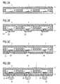
- FIGS. 3A-Dan embodiment of a complete wafer-level packaging process will be described. This embodiment not only illustrates the fabrication of the semiconductor chip module but also the fabrication of single semiconductor chip packages out of the semiconductor chip module.
- a semiconductor moduleis fabricated in principle of the embodiment as described in connection with FIGS. 1 and 2A , B. More specifically, the semiconductor chips 3 are placed onto the second layer 2 with a sufficient spacing in order to allow fan-out of the electrical contacts as will be seen later.
- a pick-and-place machinecan be used for placing the semiconductor chips 3 on the second layer 2 .
- a re-configured waferis produced during the molding process, i.e. during the fabrication of the molding material layer 5 as was illustrated in FIG. 2B .
- a mold formcan be used which has the form of a wafer so that by this kind of wafer molding, for example, a 200 mm re-configured wafer is produced.
- the semiconductor moduleis comprised of a re-configured wafer and FIG. 3A illustrates a section of this re-configured wafer in a schematic cross-section.
- contact pads 3 A of the semiconductor chips 3are illustrated.
- FIG. 3Billustrates a schematic cross-section of a section of the re-configured wafer of FIG. 3A after forming electrical conductors 2 B into the second layer 2 .
- the electrical conductors 2 Bextend through the second layer 2 and are connected with the contact pads 3 A of the semiconductor chips 3 . There will be described embodiments of forming the electrical conductors 2 B further below.
- a wiring layer 8is formed on the surface of the second layer 2 .
- the wiring layer 8includes electrically conductive contact areas 8 A connected to the electrical conductors 2 B of the second layer 2 .
- the wiring layer 8fulfills the function of a re-distribution layer as it re-distributes the arrangement of the electrical contacts to allow a spacial fan-out of the electrical contacts.
- FIG. 3Cillustrates a schematic cross-section of the section of the re-configured wafer of FIG. 3B after applying a structured solder resist layer 9 onto the electrically conductive contact areas 8 A of the wiring layer 8 and in the gaps between the contact areas 8 A.
- the solder resist layer 9is structured so that the contact areas 8 A are essentially not covered by the solder resist layer 9 . Only for simplifying the picture the area 8 A is illustrated directly over the electrical conductor 2 B.
- FIG. 3Dillustrates a schematic cross-section of the section of the re-configured wafer of FIG. 3B after applying outer electrical contacts in the form of solder balls 12 .
- the solder materialflows into the gaps between the contact areas 8 A so that the solder balls 12 are electrically connected to the contact areas 8 A of the wiring layer 8 .
- the contact areas 8 Acan be regarded as solder mask defined pads 8 A.
- the re-configured wafercan be separated into single semiconductor packages by e.g., dicing the re-configured wafer at the dashed lines.
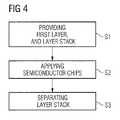
- FIG. 4illustrates a flow diagram of an embodiment of a further method for fabricating a semiconductor chip module.
- the methodincludes providing a first layer and a layer stack disposed on the first layer, the layer stack having a seed layer and a second layer (s 1 ), applying a plurality of semiconductor chips above the second layer (s 2 ), and separating the layer stack with the applied semiconductor chips from the first layer (s 3 ).
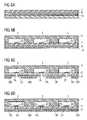
- FIGS. 5A-Cillustrate cross-section representations of intermediate products and a semiconductor chip module for illustrating a further embodiment of the embodiment of a method as illustrated in FIG. 4 .
- FIG. 5Aillustrates a layer stack having a seed layer 6 and a second layer 2 , the layer stack being applied to one of the surfaces of the first layer 1 .
- a plurality of semiconductor chips 3is applied above the second layer 2 and afterwards a material layer 5 , in one embodiment a mold layer, can be deposited onto the semiconductor chips 3 and the second layer 2 and then the layer stack with the applied semiconductor chips 3 is separated from the first layer 1 .
- the resulting semiconductor chip module and the first layer 1are illustrated in a cross-section, respectively, in FIG. 5C .
- the material layer 5can have the same properties as described above in connection with FIG. 2B .
- the first layer 1 and the layer stackcan be applied to a base layer, the plurality of semiconductor chips is applied above the second layer, and the layer stack with the applied semiconductor chips is separated from the first layer. If, however, the first layer 1 is itself a stable, rigid and handable sheet, then an extra base layer will not be needed.
- This embodimentis thus analogous to the embodiment as illustrated in FIGS. 2A , B, in which the base layer is designated with reference sign 4 .
- the seed layer 6is utilized to assist a metallization plating process, e.g., a galvanic metallization process, which is performed in a later process for the fabrication of a wiring layer.
- the seed layercan be, for example, deposited onto the second layer 2 and afterwards the first layer 1 can, for example, be laminated onto the seed layer 6 .
- the seed layer 6can be deposited as a very thin metal layer.
- the seed layer 6can be deposited as a layer stack having a 50 nm Ti layer and a 200 nm Cu layer.
- the seed layerwill not be deposited but will be generated on the surface of the second layer 2 by utilizing a specific material for the second layer, wherein the material of the second layer contains an additive, which releases electrically conducting material or releases a catalytic starter for plating upon irradiation.
- the seed layerwill be structured by laser irradiation e.g., by a scanned laser beam or by an optical imaging system (mask, lens).
- the wiring layer and electrical conductors through the second layer 2will have to be formed analogous to FIG. 3B .
- the wiring layerwill be formed by using a photoresist and lithography and a plating process.
- a photoresist layerwill be deposited onto the seed layer 6 and the photoresist layer will be structured to define areas in which contact areas of the wiring layer are to be formed.
- the photoresist layercan also be a part of the layer stack as fabricated in the beginning. In this case it is not necessary to deposit the photoresist layer in the stage as illustrated in FIG. 5C .
- This embodimentwill be described in the following.
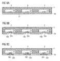
- FIGS. 6A-Dthere are illustrated schematic cross-section representations of intermediate products and a semiconductor chip module of a further embodiment of a method for fabricating a semiconductor chip module.
- a layer stackconsisting of a second layer 2 , a seed layer 6 , and a photoresist layer 10 .
- a first layer 1is laminated onto the photoresist layer 10 .
- FIG. 6Billustrates an intermediate product obtained after application of the semiconductor chips 3 and overmolding the chips 3 and the second layer 2 with the material layer 5 and separating the first layer 1 .
- an additional base layercan be used to support the layer structure as illustrated in FIG. 6A , if necessary.
- FIG. 6Cillustrates an intermediate product obtained after exposing and developing the photoresist layer 10 by conventional resist and photolithography technology to define opening areas 10 A which should become contact areas of a wiring layer to be produced and mask areas 10 B. Also illustrated are vias 2 A formed into the second layer 2 , the vias 2 A being in spatial connection with the areas 10 A.
- the vias 2 Acan, for example, be produced by ablating the material of the second layer 2 with a laser beam after structuring of the photoresist layer 10 .
- the vias 2 Acan, for example, also be produced by using the photoresist layer 10 wherein in a first lithography process the areas are defined where the vias 2 A are to be produced and in a subsequent etching process the second layer 2 is etched through the openings of the photoresist layer to produce the vias 2 A, and in a second lithography process a photoresist layer with openings 10 A and mask areas 10 B is produced as illustrated in FIG. 6C .
- FIG. 6Dillustrates an intermediate product obtained after filling the vias 2 A with a solder material or with electrically conductive ink and a subsequent metallization by using, for example, copper, to generate the contact areas 8 A of the wiring layer 8 .
- the filling of the vias 2 A with conductive inkmight also be left out when it turns out that the vias 2 A can be filled to a sufficient extent, in one embodiment without significant voids, with the galvanic metallization. In this case there will be only one metallization process for producing the contact areas 8 A and the electrically conducting via connections between the contact areas 8 A and the contact pads 3 A on the semiconductor chips 3 .
- FIG. 6Dillustrates the semiconductor chip module having plated contact areas 8 A and electrical conductors 2 B formed in the vias 2 A.
- the mask areas 10 B of the photoresist layer 10will be removed so that in this plane only the wiring layer 8 with the contact areas 8 A is left back. Afterwards the remaining areas of the seed layer 6 between the contact areas 8 A will be removed by etching. Afterwards, as was already illustrated in FIGS. 3C and D, a solder resist layer will be deposited onto the wiring layer 8 , the solder resist layer being structured such that it leaves the contact areas 8 A essentially free, and afterwards solder balls are generated on top of the solder resist layer, each one of the solder balls being connected to one of the contact areas, respectively.
- the seed layer 6 of the embodiment as described in connection with FIGS. 6A-Dwill be omitted. That means, the layer stack of FIG. 6A consists of a second layer 2 and a photoresist layer 10 . All features and processes of the embodiment of FIGS. 6A-D may be adopted besides the metallization process in FIG. 6C . As there is no seed layer, a galvanic metallization will not be possible. However, there will be other possibilities to fabricate the contact areas 8 A. For example, the contact areas 8 A might be produced by a screen printing process. Alternatively, after structuring of the photoresist layer 10 and optionally filling of the vias 2 A a solder paste might be filled into the openings 10 A of the structured photoresist layer 10 .
- FIG. 7there is illustrated a flow diagram of an embodiment of a further method for fabricating a semiconductor chip module.
- the methodincludes providing a dielectric layer, the dielectric layer having an additive, which releases electrically conducting material or catalytic starter upon irradiation (s 1 ), applying a plurality of semiconductor chips above the dielectric layer (s 2 ), and forming a plurality of electrical conductors extending through the dielectric layer to connect to contact pads on surfaces of the semiconductor chips, respectively (s 3 ).
- the dielectric layer of this embodimentincludes an additive, which releases a catalytic starter or an electrically conducting material upon irradiation with a beam of photons, ions and/or electrons.
- the additivemay include, for example, metal complexes. These metal complexes are constituents of metalorganic compounds, which can be freed from their organic constituents by heat irradiation, laser exposure and/or heat treatment of their organic constituent and are then connected as metal complexes to form conduction paths or conduction areas.
- the additivemay also include, for example, conducting nanoparticles which may be, for example, fullerenes.
- fullereneshave a hollow spherical structure of hexagonally arranged carbon atoms
- nanotubesform hollow tubes with hexagonally arranged carbon atoms on their circumference. These fullerenes or nanotubes may be exposed to form conduction paths by evaporating the surrounding plastic compound with the aid of laser processing.
- FIGS. 8A-Cthere are illustrated cross-section representations of intermediate products and semiconductor chip modules fabricated for illustrating a further embodiment of the method as illustrated in FIG. 7 .
- FIG. 8Aillustrates a cross-section of an intermediate product having a dielectric layer 20 .
- the dielectric layer 20includes an additive 21 , which releases catalytic starters or an electrically conducting material upon irradiation with a beam of electromagnetic radiation, in one embodiment a laser beam.
- the material of the dielectric layer 20can be removed or ablated by the laser beam and at the surfaces of the ablated regions the dielectric layer 20 is activated which means that at these surfaces the electrically conducting material is released so that conduction paths or conduction areas are formed.
- metal layersare deposited at the irradiated areas by using chemical plating.
- a plurality of semiconductor chips 3is arranged on a surface of the dielectric layer 20 , and a mold material layer 5 is deposited on and covering the semiconductor chips 3 and the dielectric layer 20 .
- the chips 3have at least one contact pad 3 A, respectively. Applying a release layer 1 and a carrier layer 4 could be done as described previously.
- vias 20 Aare produced in the dielectric layer 20 , the vias 20 A extending from the surface of the dielectric layer 20 to the contacts pads 3 A of the semiconductor chips 3 , respectively.
- the vias 20 Aare produced by focusing the laser beam from the side of the dielectric layer 20 on locations of the dielectric layer 20 where the vias 20 A are to be generated. At these locations the material of the dielectric layer 20 is removed or ablated so that the vias 20 A are produced and at the same time of producing the vias 20 A the irradiation of the laser beam activates the material of the dielectric layer 20 at the walls of the vias 20 A, respectively. Therefore the wavelength and intensity of the laser beam has to be selected such that it removes or ablates the material of the dielectric layer 20 and also that it activates the material at the remaining surfaces of the dielectric layer at locations where material has been removed.
- FIG. 8Balso illustrates that areas 20 B at the surface of the dielectric layer 20 adjacent to and surrounding the vias 20 A are also treated with the laser beam.
- the areas 20 Bare intended to become the contact areas of the wiring layer.
- a thin layer of the material of the dielectric layer 20is removed or ablated by the laser beam so that flat trenches are produced at the areas 20 B, respectively.
- the material of the dielectric layer 20is activated as described above. The depth of the trenches could be also nearly zero.
- FIG. 8Cillustrates the semiconductor chip module after metallization of the vias 20 A and the trenches in the areas 20 B.
- the activated layers at the walls of the vias 20 A and in the trenches of the areas 20 Bfunction as catalytic starter layers for subsequent metallization processes.
- the vias 20 Amight be filled with electrically conductive ink which also might be unnecessary for the subsequent metallization process at least as an activation or preparation of the pad surface 3 A is concerned.
- the penetration of the conductive ink into the vias 20 Acan be assisted by ultrasonic waves.
- electrical conductors 20 CAfter drying/sintering, electrical conductors 20 C have been formed wherein the vias 20 A are completely filled with the conductive ink or at least a layer having good electrical conductive properties remains on the surfaces of the vias 20 A.
- a plating processin one embodiment a chemical metallization, is carried out to grow a metallic layer in the areas 20 B and also in the vias 20 A if the vias 20 A have not been completely filled with the conductive ink.
- a plating processin one embodiment a chemical metallization
- the metallization processcan in principle also be carried out by a galvanic metallization, if all the traces could be connected to relevant current supply. With the metallization process, contact areas 20 D are produced which form together the wiring layer functioning as a redistribution layer.
- the metallic layer grown in the trenches of the areas 20 Bshould have a sufficient thickness so that the individual layers may function as contact areas 20 D of the redistribution layer. It may happen that the metallic layer is therefore grown higher than the depth of the trenches so that the metallic layer material extends over the edge portions of the trenches in a lateral direction.
- an insulating layercould be deposited on the dielectric layer 20 before the metallization, wherein the insulating layer is deposited in regions outside the areas 20 B. This will prevent that the plated metallic layer will extend in a lateral direction over the dielectric layer 20 .
- the semiconductor chip module as illustrated in FIG. 8Cis now in a condition as that illustrated in FIG. 3C of the wafer-level packaging process.
- the solder resist layercan be deposited and afterwards the solder balls can be applied.
- the modulecan be singulated to obtain a plurality of semiconductor chip packages.
- the material of the dielectric layer 20 of the embodiment of FIGS. 7 and 8is chosen and processed in a manner so that the activation of the material and the generation of conductive surface layers should function in the best possible way.
- the adhesive properties of the dielectric layer 2are not as optimal as they should be in order to fix the semiconductor chips 3 at the surface.
- an additional thin adhesive layercould be applied onto the surface of the dielectric layer 20 so that the semiconductor chips 3 could be applied to the adhesive layer.
- the adhesive layercould be made of or contain an adhesion promoter.
- the materialcould be chosen such that it can be ablated with the laser beam when forming the vias 20 A. If the thickness of adhesive layer material between the semiconductor chip 3 and the dielectric layer 20 could be bridged over in the via 20 C by the plating process, for example, the applied conductive ink as described earlier might ensure the electrical bridging for good conductivity.
- FIG. 9illustrates a flow diagram of an embodiment of a further method for fabricating a semiconductor chip module.
- the methodincludes applying a dielectric layer above an electrically conductive layer (s 1 ), applying a plurality of semiconductor chips above the dielectric layer (s 2 ), the semiconductor chips having a contact pad, respectively, structuring the electrically conductive layer so that it includes contact areas (s 3 ), and connecting each one of the contact areas with one of the contact pads, respectively (s 4 ).
- FIGS. 10A-Dthere are illustrated cross-section representations of intermediate product and a semiconductor chip module for illustrating an embodiment of the method as illustrated in FIG. 9 .
- an intermediate productis illustrated which is obtained after applying a dielectric layer 2 to an electrically conductive layer 14 and applying a plurality of semiconductor chips 3 onto the dielectric layer 2 .
- the chips 3each have at least one contact pad 3 A, respectively.
- the electrically conductive layer 14may include any electrically conductive material as, for example, a metal, a metal alloy, an organic electrically conductive material or an electrically conductive semiconductor.
- the electrically conductive layer 14may include a homogeneous constitution of a particular electrically conductive material, for example, a metallic material.
- the electrically conductive layer 14can have a stacked configuration wherein two or more layers of different electrically conductive materials are stacked one above the other.
- the electrically conductive layer 14may include a metal layer stack, as for example an alternative sequence of layers of CuNiCu, CuTiCu, . . . or any other sequence of electrically conductive layers of different material.
- the thickness of the electrically conductive layer 14can, for example, be in a range of from 10 ⁇ m to 1 mm.
- the conductive layer 14can be, for example, a metallic sheet which is itself handable and can be used as a carrier in which case no extra carrier will be needed and no release process will be necessary.
- the conductive layer 14can also be a thin layer so that a carrier is employed as was described in the embodiment illustrated in FIGS. 2 A,B.
- the semiconductor chips 3 and the dielectric layer 2are covered with a material layer 5 .
- the material of the material layer 5may include a molding material and the covering may include molding.
- the conductive layer 14is structured into contact areas 14 A and vias 14 B are formed into the conductive layer 14 and the dielectric layer 2 .
- the structuringcan be done by a conventional photolithography and etching process.
- the structures to be removedare defined by the vias 14 B and by predetermined regions 14 C surrounding the contact areas 14 A to be formed.
- a first etching processthe material of the conductive layer 14 is etched wherein the dielectric layer 2 can be used as an etch stop layer.
- a first maskis used which has openings corresponding to the predetermined regions 14 C and the vias 14 B.
- a second maskhaving openings corresponding to the vias 14 B can be used.
- the material of the dielectric layer 2is etched in order to extend the via 14 B to the contact pad 3 A of the semiconductor chip 3 .
- a laser structuring or laser ablation through the second mask having openings at the locations of the vias 14 Bcan be employed.
- the vias 14 Bare filled with an electrically conductive material like, for example, conductive ink or solder to become electrical conductors 14 D. If necessary, the empty spaces 14 C between the contact areas 14 A can be filled with an insulating material.
- the semiconductor chip module as illustrated in FIG. 10Dis now in a condition as that illustrated in FIG. 3C of the wafer-level packaging process.
- the solder resist layercan be deposited and afterwards the solder balls can be applied.
- the modulecan be singulated to obtain a plurality of semiconductor chip packages.
- the semiconductor chip package 100includes a semiconductor chip 3 having contact pads 3 A on a first surface of the chip 3 , a material layer 5 covering the semiconductor chip 3 , except for a first surface of the chip 3 , a dielectric layer 2 situated on the first surface of the chip 3 , the dielectric layer 2 having a via 2 A aligned with the contact pad 3 A, wherein the via 2 A is filled with conductive ink.
- the via 2 A filled with conductive inkforms an electrical conductor 2 B.
- the electrical conductor 2 Bcan be used to make electrical contact with a contact area 8 A which is applied to a surface of the dielectric layer 2 lying opposite to the contact 3 A of the chip 3 .
- the conductor 2 Btherefore connects the contact pad 3 A to the contact area 8 A.
- the contact area 8 Acan be an electrically conductive layer, in one embodiment a metallic layer fabricated by a plating process, like galvanic plating or chemical plating.
- there can be more than one contact pad 3 A on the surface of the semiconductor chip 3wherein all contact pads are connected by electrical conductors like the electrical conductor 2 B to contact areas like the contact area 8 A, respectively.
- a solder resist layer 9can be applied onto the dielectric layer 2 and the contact area 8 , wherein a main portion of the contact area 8 A is not covered by the solder resist layer 9 .
- the dielectric layer 2can include one or more of an acrylate material, an Epoxy-B-stage material or a material including an additive, which releases catalytic starter or electrically conducting material upon irradiation.
- the semiconductor chip package 200includes a semiconductor chip 3 having a contact pad 3 A on a first surface of the chip 3 , a material layer 5 covering the semiconductor chip 3 , except for a first surface of the chip 3 , and a dielectric layer 30 situated above the first surface of the chip 3 , wherein the dielectric layer 30 includes one or more of an acrylate material, an Epoxy-B-stage material, or a material including an additive or additives, which releases catalytic starter or electrically conducting material upon irradiation.
- the dielectric layer 30may include a via 30 A aligned with the contact pad 3 A, wherein the via 30 A can be filled with conductive material, e.g., conductive ink.
- the via 30 A filled with conductive inkforms an electrical conductor 30 B.
- the electrical conductor 30 Bcan be used to make electrical contact with a contact area 8 A which is applied to a surface of the dielectric layer 30 lying opposite to the contact 3 A of the chip 3 .
- the conductor 30 Btherefore connects the contact pad 3 A to the contact area 8 A.
- the contact area 8 Acan be an electrically conductive layer, in one embodiment a metallic layer fabricated by a plating process, like galvanic plating or chemical plating.
- a solder resist layer 9can be applied onto the dielectric layer 30 and the contact area 8 , wherein a main portion of the contact area 8 A is not covered by the solder resist layer 9 .
- the semiconductor chip package 100( FIG. 11 ) or 200 ( FIG. 12 ) may have more than one redistribution layer.
- the semiconductor chip package 100 or 200may include more than one chip and may include also passive components.
- the semiconductor chip packagemay have vias through the material layer (cover layer) 5 and the material layer 5 might have metal and/or dielectric structures at the opposite side of the first side of the chip 3 .
- the semiconductor chip packagemight be not fully covered by the material layer 5 and might leave the backside of the chip 3 uncovered so that the backside of the chip 3 is exposed.
- the material layer 5might be not parallel to the first side of the chip 3 , it might be structured 3-dimensional.
Landscapes
- Engineering & Computer Science (AREA)
- Microelectronics & Electronic Packaging (AREA)
- Computer Hardware Design (AREA)
- Power Engineering (AREA)
- Physics & Mathematics (AREA)
- Condensed Matter Physics & Semiconductors (AREA)
- General Physics & Mathematics (AREA)
- Manufacturing & Machinery (AREA)
- Internal Circuitry In Semiconductor Integrated Circuit Devices (AREA)
- Encapsulation Of And Coatings For Semiconductor Or Solid State Devices (AREA)
- Structures Or Materials For Encapsulating Or Coating Semiconductor Devices Or Solid State Devices (AREA)
Abstract
Description
- The present invention relates to a method for fabricating a semiconductor chip module and a semiconductor chip package.
- Semiconductor chips have contact pads on one or more of their surfaces. When housing the semiconductor chip in a chip package, the contact pads of the semiconductor chip have to be connected to external contact elements of the chip package.
- For these and other reasons, there is a need for the present invention.
- The accompanying drawings are included to provide a further understanding of embodiments and are incorporated in and constitute a part of this specification. The drawings illustrate embodiments and together with the description serve to explain principles of embodiments. Other embodiments and many of the intended advantages of embodiments will be readily appreciated as they become better understood by reference to the following detailed description. The elements of the drawings are not necessarily to scale relative to each other. Like reference numerals designate corresponding similar parts.
FIG. 1 illustrates a flow diagram of an embodiment of a method for fabricating a semiconductor chip module;FIGS. 2A , B illustrate schematic cross-section representations of an intermediate product and the semiconductor chip module for illustrating a further embodiment as illustrated inFIG. 1 ;FIGS. 3A-D illustrate schematic cross-section representations of a semiconductor chip module for illustrating a further embodiment of the method as illustrated inFIGS. 2A , B;FIG. 4 illustrates a flow diagram of an embodiment of a further method for fabricating a semiconductor chip module;FIGS. 5A-C illustrate cross-section representations of intermediate products and the semiconductor chip module for illustrating a further embodiment of the method as illustrated inFIG. 4 ;FIGS. 6A-D illustrate cross-section representations of the semiconductor chip module for illustrating a further embodiment of the method as illustrated inFIGS. 4 and 5 ;FIG. 7 illustrates a flow diagram of an embodiment of a further method for fabricating a semiconductor chip module;FIG. 8A-C illustrates cross-section representations of the semiconductor chip module for illustrating a further embodiment of a method as illustrated inFIG. 7 ;FIG. 9 illustrates a flow diagram of an embodiment of a further method for fabricating a semiconductor chip module;FIGS. 10A-D illustrate cross-section representations of an intermediate product and the semiconductor chip module for illustrating a further embodiment of the method as illustrated inFIG. 9 ;FIG. 11 illustrates a schematic cross-section representation of an embodiment of a semiconductor chip package;FIG. 12 illustrates a schematic cross-section representation of a further embodiment of the semiconductor chip package ofFIG. 11 .- In the following Detailed Description, reference is made to the accompanying drawings, which form a part hereof, and in which is shown by way of illustration specific embodiments in which the invention may be practiced. In this regard, directional terminology, such as “top,” “bottom,” “front,” “back,” “leading,” “trailing,” etc., is used with reference to the orientation of the Figure(s) being described. Because components of embodiments can be positioned in a number of different orientations, the directional terminology is used for purposes of illustration and is in no way limiting. It is to be understood that other embodiments may be utilized and structural or logical changes may be made without departing from the scope of the present invention. The following detailed description, therefore, is not to be taken in a limiting sense, and the scope of the present invention is defined by the appended claims.
- It is to be understood that the features of the various exemplary embodiments described herein may be combined with each other, unless specifically noted otherwise.
- The embodiments of a method for fabricating a semiconductor chip module and the embodiments of a semiconductor chip package may use various types of semiconductor chips or semiconductor substrates, among them logic integrated circuits, analog integrated circuits, mixed signal integrated circuits, sensor circuits, MEMS (Micro-Electro-Mechanical Systems), power integrated circuits, chips with integrated passives etc.
- In several embodiments layers or layer stacks are applied to one another or materials are applied or deposited onto layers. It should be appreciated that any such terms as “applied” or “deposited” are meant to cover literally all kinds and techniques of applying layers onto each other. In one embodiment, they are meant to cover techniques in which layers are applied at once as a whole, like, for example, laminating techniques, as well as techniques in which layers are deposited in a sequential manner, like, for example, sputtering, plating, molding, CVD, etc.
- The semiconductor chips may have contact elements or contact pads on one or more of their outer surfaces wherein the contact elements serve for electrically contacting the semiconductor chips. The contact elements may be made from any electrically conducting material, e.g., from a metal as aluminum, gold, or copper, for example, or a metal alloy, or an electrically conducting organic material, or an electrically conducting semiconductor material.
- The semiconductor chips may be covered with a material layer. The material of the material layer can be any electrically insulating material like, for example, any kind of molding material, any kind of epoxy material, or any kind of resin material. In the process of covering the semiconductor chips with the material layer a fan-out embedded die can be fabricated. The fan-out embedded die can have the form of a wafer and will thus be called a “re-configured wafer” further below. However, it will be appreciated that the fan-out embedded die is not limited to the form and shape of a wafer but can have any size and shape and any suitable array of semiconductor chips embedded therein.
FIG. 1 illustrates a flow diagram of an embodiment of a method for fabricating a semiconductor chip module. The method includes providing a first layer, a second layer, and a base layer, wherein the first layer is disposed on the second layer, and the second layer is disposed on the base layer (s1), applying a plurality of semiconductor chips above the second layer (s2), and separating the second layer with the applied semiconductor chips from the first layer (s3).- The method as illustrated in the flow diagram of
FIG. 1 is further illustrated in FIG.2A,B. FIGS.2A,B illustrate schematic cross-section representations of an intermediate product and a semiconductor chip module for illustrating a further embodiment of the method as illustrated inFIG. 1 . OfFIG. 2A , there is illustrated an intermediate product after applying of afirst layer 1 to abase layer 4 and applying asecond layer 2 on thefirst layer 1 and applying a plurality ofsemiconductor chips 3 onto thesecond layer 2 and thesemiconductor chips 3 can be encapsulated by amaterial layer 5 or coverlayer 5 as will be outlined further below. OfFIG. 2B , thesecond layer 2 with the appliedsemiconductor chips 3 is separated from thefirst layer 1. The semiconductor chips3 are illustrated each one having onecontact pad 3A. It should be clear that thesemiconductor chips 3 can have more than one contact pad. - The provision of the
first layer 1, thesecond layer 2, and thebase layer 4 as illustrated inFIG. 2A can be as follows. Thefirst layer 2 and thesecond layer 2 are applied to one another, for example, by laminatingfirst layer 1 tosecond layer 2, or vice versa. A commercially available pre-configured layer stack having thefirst layer 1 and thesecond layer 2 can be purchased. Then the layer stack having thefirst layer 1 and thesecond layer 2 is applied, in one embodiment laminated, to thebase layer 4. Alternatively, thefirst layer 1 can be first applied, in one embodiment laminated, to thebase layer 4 and afterwards thesecond layer 2 can be applied, in one embodiment laminated, to thefirst layer 1. - According to one embodiment as illustrated in FIGS.2A,B, the
first layer 1 is also separated from thebase layer 4. In such a case thebase layer 4 can be re-used. However, it is also possible that thefirst layer 1 remains on thebase layer 4 so that in most cases thebase layer 4 will not be in a condition to be re-used. - It is also illustrated in
FIG. 2B that amaterial layer 5 is deposited onto thesemiconductor chips 3 and thesecond layer 2. Thematerial layer 5 can, for example, include a molding material wherein the molding technique can be, for example, compression molding. The potential molding materials include, for example, aliphatic and aromatic polymers including thermoplastic and thermoset type polymers and blends of these and also other various type of polymers. Furthermore, thesecond layer 2 may have a constitution so that it reacts with the mold compound in order to provide for a strong mechanical connection between thematerial layer 5 and thesecond layer 2. Moreover, thesecond layer 2 may be constituted such that it reacts with the surfaces of thesemiconductor chips 3 during the molding and/or during the hardening of the mold compound in order to provide for a best reliable adhesion between thesemiconductor chips 3 and thesecond layer 2. - Typical values for the thicknesses of the layers may be as follows. The thickness of the
first layer 1 and thesecond layer 2 is typically ranges from 5 μm to 150 μm, whereas the thickness of the semiconductor chips typically ranges from 150 μm to 450 μm, and the thickness of the mold material layer typically ranges from 300 μm to 700 μm. - The
base layer 4 may include, for example, any structural material, such as, for example, plastic, ceramic, or metal. However, further below there will be illustrated and explained further methods for fabricating a semiconductor chip module, which do not require thebase layer 4. - The
second layer 2 can be utilized, as will be illustrated further below, as an interconnect layer in a fan-out embedded die as will be further described below. That means, thesecond layer 2 carries thesemiconductor chips 3 during the production of the re-configured wafer and also functions as the interconnect layer in the fan-out wafer-level package to be produced. For this purpose thesecond layer 2 needs to be made of a dielectric, insulating material which can be structured in order to access electrical conductors therein by means which will be outlined in further embodiments below. The two functions of thesecond layer 2 can, for example, be fulfilled with foils based on an acrylate or Epoxy-B-stage foils. Thesecond layer 2, for example, can also be made from a prepreg (preimprgnated) foil, such as that known from substrate technology, e.g., a photostructurable prepreg which can be etched after lithographical exposure. Alternatively thesecond layer 2 could be ablated and structured with a laser beam. Thesecond layer 2 can also include an additive, which releases electrically conducting material or releases a catalytic layer for plating upon irradiation. Thesecond layer 2 should also have sufficient adhesion properties in order to fix thesemiconductor chips 3 on its surface. If, however, thesecond layer 2 does not have itself sufficient adhesion force at its surface, a third layer (not illustrated) having an adhesion promoter can be applied to the surface of thesecond layer 2. - The
first layer 1 may function as a release layer. In one embodiment, it may include a release system so that upon external predetermined conditions like, for example, heat or UV radiation, thefirst layer 1 can be released from thesecond layer 2 and also, if desired, from thebase layer 4. Heat or UV radiation can be applied from below thebase layer 4 so that in case of thefirst layer 1 being a thermal release tape thebase layer 4 needs not to be optically transparent whereas in case of thefirst layer 1 being an UV light release tape,base layer 4 must be optically transparent for UV radiation. It is also possible that thefirst layer 1 has a release system only on the side towards thebase layer 4 and the separation from thesecond layer 2 is accomplished as known from conventional adhesive film technology. - In a further embodiment of the method as illustrated in
FIGS. 3A-D , an embodiment of a complete wafer-level packaging process will be described. This embodiment not only illustrates the fabrication of the semiconductor chip module but also the fabrication of single semiconductor chip packages out of the semiconductor chip module. - First of all, a semiconductor module is fabricated in principle of the embodiment as described in connection with
FIGS. 1 and 2A , B. More specifically, thesemiconductor chips 3 are placed onto thesecond layer 2 with a sufficient spacing in order to allow fan-out of the electrical contacts as will be seen later. A pick-and-place machine can be used for placing thesemiconductor chips 3 on thesecond layer 2. - In the following, a re-configured wafer is produced during the molding process, i.e. during the fabrication of the
molding material layer 5 as was illustrated inFIG. 2B . For example, a mold form can be used which has the form of a wafer so that by this kind of wafer molding, for example, a 200 mm re-configured wafer is produced. Thus the semiconductor module is comprised of a re-configured wafer andFIG. 3A illustrates a section of this re-configured wafer in a schematic cross-section. In addition there are illustratedcontact pads 3A of thesemiconductor chips 3. FIG. 3B illustrates a schematic cross-section of a section of the re-configured wafer ofFIG. 3A after formingelectrical conductors 2B into thesecond layer 2. Theelectrical conductors 2B extend through thesecond layer 2 and are connected with thecontact pads 3A of thesemiconductor chips 3. There will be described embodiments of forming theelectrical conductors 2B further below. After forming of theelectrical conductors 2B, a wiring layer8 is formed on the surface of thesecond layer 2. The wiring layer8 includes electricallyconductive contact areas 8A connected to theelectrical conductors 2B of thesecond layer 2. The wiring layer8 fulfills the function of a re-distribution layer as it re-distributes the arrangement of the electrical contacts to allow a spacial fan-out of the electrical contacts.FIG. 3C illustrates a schematic cross-section of the section of the re-configured wafer ofFIG. 3B after applying a structured solder resistlayer 9 onto the electricallyconductive contact areas 8A of the wiring layer8 and in the gaps between thecontact areas 8A. The solder resistlayer 9 is structured so that thecontact areas 8A are essentially not covered by the solder resistlayer 9. Only for simplifying the picture thearea 8A is illustrated directly over theelectrical conductor 2B.FIG. 3D illustrates a schematic cross-section of the section of the re-configured wafer ofFIG. 3B after applying outer electrical contacts in the form ofsolder balls 12. When producing thesolder balls 12, the solder material flows into the gaps between thecontact areas 8A so that thesolder balls 12 are electrically connected to thecontact areas 8A of the wiring layer8. In this case thecontact areas 8A can be regarded as solder mask definedpads 8A. Next, the re-configured wafer can be separated into single semiconductor packages by e.g., dicing the re-configured wafer at the dashed lines.FIG. 4 illustrates a flow diagram of an embodiment of a further method for fabricating a semiconductor chip module. The method includes providing a first layer and a layer stack disposed on the first layer, the layer stack having a seed layer and a second layer (s1), applying a plurality of semiconductor chips above the second layer (s2), and separating the layer stack with the applied semiconductor chips from the first layer (s3).FIGS. 5A-C illustrate cross-section representations of intermediate products and a semiconductor chip module for illustrating a further embodiment of the embodiment of a method as illustrated inFIG. 4 .FIG. 5A illustrates a layer stack having aseed layer 6 and asecond layer 2, the layer stack being applied to one of the surfaces of thefirst layer 1. OfFIG. 5B , a plurality ofsemiconductor chips 3 is applied above thesecond layer 2 and afterwards amaterial layer 5, in one embodiment a mold layer, can be deposited onto thesemiconductor chips 3 and thesecond layer 2 and then the layer stack with the appliedsemiconductor chips 3 is separated from thefirst layer 1. The resulting semiconductor chip module and thefirst layer 1 are illustrated in a cross-section, respectively, inFIG. 5C .- The
material layer 5 can have the same properties as described above in connection withFIG. 2B . - In a further embodiment of the method as illustrated in
FIGS. 4 and 5 , thefirst layer 1 and the layer stack can be applied to a base layer, the plurality of semiconductor chips is applied above the second layer, and the layer stack with the applied semiconductor chips is separated from the first layer. If, however, thefirst layer 1 is itself a stable, rigid and handable sheet, then an extra base layer will not be needed. This embodiment is thus analogous to the embodiment as illustrated inFIGS. 2A , B, in which the base layer is designated withreference sign 4. - All further embodiments which were described in connection with
FIGS. 1 and 2 , in one embodiment as regards thefirst layer 1 and thesecond layer 2 can also be applied to the embodiment ofFIGS. 4 and 5 . - The
seed layer 6 is utilized to assist a metallization plating process, e.g., a galvanic metallization process, which is performed in a later process for the fabrication of a wiring layer. The seed layer can be, for example, deposited onto thesecond layer 2 and afterwards thefirst layer 1 can, for example, be laminated onto theseed layer 6. In this case, theseed layer 6 can be deposited as a very thin metal layer. For example, theseed layer 6 can be deposited as a layer stack having a 50 nm Ti layer and a 200 nm Cu layer. In a further embodiment which will be described further below, the seed layer will not be deposited but will be generated on the surface of thesecond layer 2 by utilizing a specific material for the second layer, wherein the material of the second layer contains an additive, which releases electrically conducting material or releases a catalytic starter for plating upon irradiation. Also as described further below such seed layer will be structured by laser irradiation e.g., by a scanned laser beam or by an optical imaging system (mask, lens). - In the next process following
FIG. 5C , the wiring layer and electrical conductors through thesecond layer 2 will have to be formed analogous toFIG. 3B . The wiring layer will be formed by using a photoresist and lithography and a plating process. For this purpose a photoresist layer will be deposited onto theseed layer 6 and the photoresist layer will be structured to define areas in which contact areas of the wiring layer are to be formed. - As an alternative to the embodiment as illustrated in
FIGS. 5A-C , the photoresist layer can also be a part of the layer stack as fabricated in the beginning. In this case it is not necessary to deposit the photoresist layer in the stage as illustrated inFIG. 5C . This embodiment will be described in the following. - In
FIGS. 6A-D there are illustrated schematic cross-section representations of intermediate products and a semiconductor chip module of a further embodiment of a method for fabricating a semiconductor chip module. InFIG. 6A there is illustrated a layer stack consisting of asecond layer 2, aseed layer 6, and aphotoresist layer 10. Afirst layer 1 is laminated onto thephotoresist layer 10.FIG. 6B illustrates an intermediate product obtained after application of thesemiconductor chips 3 and overmolding thechips 3 and thesecond layer 2 with thematerial layer 5 and separating thefirst layer 1. As explained in connection with previous embodiments, an additional base layer can be used to support the layer structure as illustrated inFIG. 6A , if necessary. FIG. 6C illustrates an intermediate product obtained after exposing and developing thephotoresist layer 10 by conventional resist and photolithography technology to define openingareas 10A which should become contact areas of a wiring layer to be produced andmask areas 10B. Also illustrated are vias2A formed into thesecond layer 2, thevias 2A being in spatial connection with theareas 10A. Thevias 2A can, for example, be produced by ablating the material of thesecond layer 2 with a laser beam after structuring of thephotoresist layer 10. However, thevias 2A can, for example, also be produced by using thephotoresist layer 10 wherein in a first lithography process the areas are defined where thevias 2A are to be produced and in a subsequent etching process thesecond layer 2 is etched through the openings of the photoresist layer to produce thevias 2A, and in a second lithography process a photoresist layer withopenings 10A andmask areas 10B is produced as illustrated inFIG. 6C .FIG. 6D illustrates an intermediate product obtained after filling thevias 2A with a solder material or with electrically conductive ink and a subsequent metallization by using, for example, copper, to generate thecontact areas 8A of the wiring layer8. The filling of thevias 2A with conductive ink might also be left out when it turns out that thevias 2A can be filled to a sufficient extent, in one embodiment without significant voids, with the galvanic metallization. In this case there will be only one metallization process for producing thecontact areas 8A and the electrically conducting via connections between thecontact areas 8A and thecontact pads 3A on thesemiconductor chips 3.FIG. 6D illustrates the semiconductor chip module having platedcontact areas 8A andelectrical conductors 2B formed in thevias 2A.- In the next process which is carried out after the intermediate product of
FIG. 6D has been obtained, themask areas 10B of thephotoresist layer 10 will be removed so that in this plane only the wiring layer8 with thecontact areas 8A is left back. Afterwards the remaining areas of theseed layer 6 between thecontact areas 8A will be removed by etching. Afterwards, as was already illustrated inFIGS. 3C and D, a solder resist layer will be deposited onto the wiring layer8, the solder resist layer being structured such that it leaves thecontact areas 8A essentially free, and afterwards solder balls are generated on top of the solder resist layer, each one of the solder balls being connected to one of the contact areas, respectively. - In a further embodiment of a method for fabricating a semiconductor chip module, the
seed layer 6 of the embodiment as described in connection withFIGS. 6A-D will be omitted. That means, the layer stack ofFIG. 6A consists of asecond layer 2 and aphotoresist layer 10. All features and processes of the embodiment ofFIGS. 6A-D may be adopted besides the metallization process inFIG. 6C . As there is no seed layer, a galvanic metallization will not be possible. However, there will be other possibilities to fabricate thecontact areas 8A. For example, thecontact areas 8A might be produced by a screen printing process. Alternatively, after structuring of thephotoresist layer 10 and optionally filling of thevias 2A a solder paste might be filled into theopenings 10A of the structuredphotoresist layer 10. - Referring to
FIG. 7 , there is illustrated a flow diagram of an embodiment of a further method for fabricating a semiconductor chip module. The method includes providing a dielectric layer, the dielectric layer having an additive, which releases electrically conducting material or catalytic starter upon irradiation (s1), applying a plurality of semiconductor chips above the dielectric layer (s2), and forming a plurality of electrical conductors extending through the dielectric layer to connect to contact pads on surfaces of the semiconductor chips, respectively (s3). - The dielectric layer of this embodiment includes an additive, which releases a catalytic starter or an electrically conducting material upon irradiation with a beam of photons, ions and/or electrons. The additive may include, for example, metal complexes. These metal complexes are constituents of metalorganic compounds, which can be freed from their organic constituents by heat irradiation, laser exposure and/or heat treatment of their organic constituent and are then connected as metal complexes to form conduction paths or conduction areas. The additive may also include, for example, conducting nanoparticles which may be, for example, fullerenes. While fullerenes have a hollow spherical structure of hexagonally arranged carbon atoms, nanotubes form hollow tubes with hexagonally arranged carbon atoms on their circumference. These fullerenes or nanotubes may be exposed to form conduction paths by evaporating the surrounding plastic compound with the aid of laser processing.
- Referring to
FIGS. 8A-C , there are illustrated cross-section representations of intermediate products and semiconductor chip modules fabricated for illustrating a further embodiment of the method as illustrated inFIG. 7 .FIG. 8A illustrates a cross-section of an intermediate product having adielectric layer 20. Of this embodiment thedielectric layer 20 includes an additive21, which releases catalytic starters or an electrically conducting material upon irradiation with a beam of electromagnetic radiation, in one embodiment a laser beam. The material of thedielectric layer 20 can be removed or ablated by the laser beam and at the surfaces of the ablated regions thedielectric layer 20 is activated which means that at these surfaces the electrically conducting material is released so that conduction paths or conduction areas are formed. In case of a catalytic starter, metal layers are deposited at the irradiated areas by using chemical plating. - Of
FIG. 8A , a plurality ofsemiconductor chips 3 is arranged on a surface of thedielectric layer 20, and amold material layer 5 is deposited on and covering thesemiconductor chips 3 and thedielectric layer 20. Thechips 3 have at least onecontact pad 3A, respectively. Applying arelease layer 1 and acarrier layer 4 could be done as described previously. - In the following, the fabrication of a wiring layer will be described which functions as a redistribution layer. Of
FIG. 8B , vias20A are produced in thedielectric layer 20, thevias 20A extending from the surface of thedielectric layer 20 to thecontacts pads 3A of thesemiconductor chips 3, respectively. Thevias 20A are produced by focusing the laser beam from the side of thedielectric layer 20 on locations of thedielectric layer 20 where thevias 20A are to be generated. At these locations the material of thedielectric layer 20 is removed or ablated so that thevias 20A are produced and at the same time of producing thevias 20A the irradiation of the laser beam activates the material of thedielectric layer 20 at the walls of the vias20A, respectively. Therefore the wavelength and intensity of the laser beam has to be selected such that it removes or ablates the material of thedielectric layer 20 and also that it activates the material at the remaining surfaces of the dielectric layer at locations where material has been removed. FIG. 8B also illustrates thatareas 20B at the surface of thedielectric layer 20 adjacent to and surrounding thevias 20A are also treated with the laser beam. Theareas 20B are intended to become the contact areas of the wiring layer. In theareas 20B a thin layer of the material of thedielectric layer 20 is removed or ablated by the laser beam so that flat trenches are produced at theareas 20B, respectively. At the bottom and side surfaces of the trenches the material of thedielectric layer 20 is activated as described above. The depth of the trenches could be also nearly zero.FIG. 8C illustrates the semiconductor chip module after metallization of the vias20A and the trenches in theareas 20B. The activated layers at the walls of thevias 20A and in the trenches of theareas 20B function as catalytic starter layers for subsequent metallization processes. In a first process, thevias 20A might be filled with electrically conductive ink which also might be unnecessary for the subsequent metallization process at least as an activation or preparation of thepad surface 3A is concerned. The penetration of the conductive ink into thevias 20A can be assisted by ultrasonic waves. After drying/sintering,electrical conductors 20C have been formed wherein thevias 20A are completely filled with the conductive ink or at least a layer having good electrical conductive properties remains on the surfaces of thevias 20A. Then in a second process, a plating process, in one embodiment a chemical metallization, is carried out to grow a metallic layer in theareas 20B and also in thevias 20A if thevias 20A have not been completely filled with the conductive ink. In principle it is also possible to omit the process of filling conductive ink into thevias 20A and instead to carry out the chemical metallization from the beginning. The metallization process can in principle also be carried out by a galvanic metallization, if all the traces could be connected to relevant current supply. With the metallization process, contactareas 20D are produced which form together the wiring layer functioning as a redistribution layer.- The metallic layer grown in the trenches of the
areas 20B should have a sufficient thickness so that the individual layers may function ascontact areas 20D of the redistribution layer. It may happen that the metallic layer is therefore grown higher than the depth of the trenches so that the metallic layer material extends over the edge portions of the trenches in a lateral direction. In order to prevent this scenario, an insulating layer could be deposited on thedielectric layer 20 before the metallization, wherein the insulating layer is deposited in regions outside theareas 20B. This will prevent that the plated metallic layer will extend in a lateral direction over thedielectric layer 20. - The semiconductor chip module as illustrated in
FIG. 8C is now in a condition as that illustrated inFIG. 3C of the wafer-level packaging process. At next, analogous toFIG. 3D , the solder resist layer can be deposited and afterwards the solder balls can be applied. At the end, the module can be singulated to obtain a plurality of semiconductor chip packages. - The material of the
dielectric layer 20 of the embodiment ofFIGS. 7 and 8 is chosen and processed in a manner so that the activation of the material and the generation of conductive surface layers should function in the best possible way. As this is the main property of the dielectric layer to observed, it may be the case that the adhesive properties of thedielectric layer 2 are not as optimal as they should be in order to fix thesemiconductor chips 3 at the surface. In this case an additional thin adhesive layer could be applied onto the surface of thedielectric layer 20 so that thesemiconductor chips 3 could be applied to the adhesive layer. The adhesive layer could be made of or contain an adhesion promoter. The material could be chosen such that it can be ablated with the laser beam when forming thevias 20A. If the thickness of adhesive layer material between thesemiconductor chip 3 and thedielectric layer 20 could be bridged over in the via20C by the plating process, for example, the applied conductive ink as described earlier might ensure the electrical bridging for good conductivity. FIG. 9 illustrates a flow diagram of an embodiment of a further method for fabricating a semiconductor chip module. The method includes applying a dielectric layer above an electrically conductive layer (s1), applying a plurality of semiconductor chips above the dielectric layer (s2), the semiconductor chips having a contact pad, respectively, structuring the electrically conductive layer so that it includes contact areas (s3), and connecting each one of the contact areas with one of the contact pads, respectively (s4).- Referring to
FIGS. 10A-D , there are illustrated cross-section representations of intermediate product and a semiconductor chip module for illustrating an embodiment of the method as illustrated inFIG. 9 . InFIG. 10A an intermediate product is illustrated which is obtained after applying adielectric layer 2 to an electricallyconductive layer 14 and applying a plurality ofsemiconductor chips 3 onto thedielectric layer 2. Thechips 3 each have at least onecontact pad 3A, respectively. - The electrically
conductive layer 14 may include any electrically conductive material as, for example, a metal, a metal alloy, an organic electrically conductive material or an electrically conductive semiconductor. The electricallyconductive layer 14 may include a homogeneous constitution of a particular electrically conductive material, for example, a metallic material. Alternatively the electricallyconductive layer 14 can have a stacked configuration wherein two or more layers of different electrically conductive materials are stacked one above the other. For example, the electricallyconductive layer 14 may include a metal layer stack, as for example an alternative sequence of layers of CuNiCu, CuTiCu, . . . or any other sequence of electrically conductive layers of different material. The thickness of the electricallyconductive layer 14 can, for example, be in a range of from 10 μm to 1 mm. Theconductive layer 14 can be, for example, a metallic sheet which is itself handable and can be used as a carrier in which case no extra carrier will be needed and no release process will be necessary. Theconductive layer 14 can also be a thin layer so that a carrier is employed as was described in the embodiment illustrated in FIGS.2A,B. - In
FIG. 10B , thesemiconductor chips 3 and thedielectric layer 2 are covered with amaterial layer 5. The material of thematerial layer 5 may include a molding material and the covering may include molding. - In
FIG. 10C , theconductive layer 14 is structured intocontact areas 14A andvias 14B are formed into theconductive layer 14 and thedielectric layer 2. The structuring can be done by a conventional photolithography and etching process. The structures to be removed are defined by thevias 14B and bypredetermined regions 14C surrounding thecontact areas 14A to be formed. In a first etching process the material of theconductive layer 14 is etched wherein thedielectric layer 2 can be used as an etch stop layer. In the first etching process a first mask is used which has openings corresponding to thepredetermined regions 14C and thevias 14B. Then in a second etching process a second mask having openings corresponding to thevias 14B can be used. In the second etching process the material of thedielectric layer 2 is etched in order to extend the via14B to thecontact pad 3A of thesemiconductor chip 3. Alternatively, instead of applying a second etching process for etching through the dielectric layer, also a laser structuring or laser ablation through the second mask having openings at the locations of the vias14B, can be employed. - In
FIG. 10D , thevias 14B are filled with an electrically conductive material like, for example, conductive ink or solder to becomeelectrical conductors 14D. If necessary, theempty spaces 14C between thecontact areas 14A can be filled with an insulating material. - The semiconductor chip module as illustrated in
FIG. 10D is now in a condition as that illustrated inFIG. 3C of the wafer-level packaging process. At next, analogous toFIG. 3D , the solder resist layer can be deposited and afterwards the solder balls can be applied. At the end the module can be singulated to obtain a plurality of semiconductor chip packages. - Referring to
FIG. 11 , a schematic cross-section representation of an embodiment of a semiconductor chip package is illustrated. Thesemiconductor chip package 100 includes asemiconductor chip 3 havingcontact pads 3A on a first surface of thechip 3, amaterial layer 5 covering thesemiconductor chip 3, except for a first surface of thechip 3, adielectric layer 2 situated on the first surface of thechip 3, thedielectric layer 2 having a via2A aligned with thecontact pad 3A, wherein the via2A is filled with conductive ink. - The via2A filled with conductive ink forms an
electrical conductor 2B. Theelectrical conductor 2B can be used to make electrical contact with acontact area 8A which is applied to a surface of thedielectric layer 2 lying opposite to thecontact 3A of thechip 3. Theconductor 2B therefore connects thecontact pad 3A to thecontact area 8A. Thecontact area 8A can be an electrically conductive layer, in one embodiment a metallic layer fabricated by a plating process, like galvanic plating or chemical plating. As indicated above, there can be more than onecontact pad 3A on the surface of thesemiconductor chip 3, wherein all contact pads are connected by electrical conductors like theelectrical conductor 2B to contact areas like thecontact area 8A, respectively. Furthermore, as illustrated in the embodiment ofFIG. 11 , a solder resistlayer 9 can be applied onto thedielectric layer 2 and the contact area8, wherein a main portion of thecontact area 8A is not covered by the solder resistlayer 9. - The
dielectric layer 2 can include one or more of an acrylate material, an Epoxy-B-stage material or a material including an additive, which releases catalytic starter or electrically conducting material upon irradiation. - Referring to
FIG. 12 , a schematic cross-section representation of a further embodiment of a semiconductor chip package is illustrated. Thesemiconductor chip package 200 includes asemiconductor chip 3 having acontact pad 3A on a first surface of thechip 3, amaterial layer 5 covering thesemiconductor chip 3, except for a first surface of thechip 3, and adielectric layer 30 situated above the first surface of thechip 3, wherein thedielectric layer 30 includes one or more of an acrylate material, an Epoxy-B-stage material, or a material including an additive or additives, which releases catalytic starter or electrically conducting material upon irradiation. - As further illustrated in
FIG. 12 , thedielectric layer 30 may include a via30A aligned with thecontact pad 3A, wherein the via30A can be filled with conductive material, e.g., conductive ink. The via30A filled with conductive ink forms anelectrical conductor 30B. Theelectrical conductor 30B can be used to make electrical contact with acontact area 8A which is applied to a surface of thedielectric layer 30 lying opposite to thecontact 3A of thechip 3. Theconductor 30B therefore connects thecontact pad 3A to thecontact area 8A. Thecontact area 8A can be an electrically conductive layer, in one embodiment a metallic layer fabricated by a plating process, like galvanic plating or chemical plating. As indicated above, there can be more than onecontact pad 3A on the surface of thesemiconductor chip 3, wherein all contact pads are connected by electrical conductors like theelectrical conductor 30B to contact areas like thecontact area 8A, respectively. Furthermore, as illustrated in the embodiment ofFIG. 12 , a solder resistlayer 9 can be applied onto thedielectric layer 30 and the contact area8, wherein a main portion of thecontact area 8A is not covered by the solder resistlayer 9. - The semiconductor chip package100 (
FIG. 11 ) or200 (FIG. 12 ) may have more than one redistribution layer. Thesemiconductor chip package material layer 5 might have metal and/or dielectric structures at the opposite side of the first side of thechip 3. The semiconductor chip package might be not fully covered by thematerial layer 5 and might leave the backside of thechip 3 uncovered so that the backside of thechip 3 is exposed. Thematerial layer 5 might be not parallel to the first side of thechip 3, it might be structured 3-dimensional. - Although specific embodiments have been illustrated and described herein, it will be appreciated by those of ordinary skill in the art that a variety of alternate and/or equivalent implementations may be substituted for the specific embodiments shown and described without departing from the scope of the present invention. This application is intended to cover any adaptations or variations of the specific embodiments discussed herein. Therefore, it is intended that this invention be limited only by the claims and the equivalents thereof
Claims (57)
Priority Applications (9)
| Application Number | Priority Date | Filing Date | Title |
|---|---|---|---|
| US11/837,211US8258624B2 (en) | 2007-08-10 | 2007-08-10 | Method for fabricating a semiconductor and semiconductor package |
| DE102007040149.5ADE102007040149B4 (en) | 2007-08-10 | 2007-08-24 | Method for producing a semiconductor chip module and a semiconductor chip package |
| US12/947,031US8216881B2 (en) | 2007-08-10 | 2010-11-16 | Method for fabricating a semiconductor and semiconductor package |
| US13/529,315US8492200B2 (en) | 2007-08-10 | 2012-06-21 | Method for fabricating a semiconductor and semiconductor package |
| US13/570,986US8658468B2 (en) | 2007-08-10 | 2012-08-09 | Method for fabricating a semiconductor and semiconductor package |
| US13/909,727US8728869B2 (en) | 2007-08-10 | 2013-06-04 | Method for fabricating a semiconductor device and semiconductor package |
| US14/154,668US10438926B2 (en) | 2007-08-10 | 2014-01-14 | Method for fabricating a semiconductor and semiconductor package |
| US16/542,247US10643971B2 (en) | 2007-08-10 | 2019-08-15 | Method for fabricating a semiconductor and semiconductor package |
| US16/839,404US10957671B2 (en) | 2007-08-10 | 2020-04-03 | Method for fabricating a semiconductor and semiconductor package |
Applications Claiming Priority (1)
| Application Number | Priority Date | Filing Date | Title |
|---|---|---|---|
| US11/837,211US8258624B2 (en) | 2007-08-10 | 2007-08-10 | Method for fabricating a semiconductor and semiconductor package |
Related Parent Applications (2)
| Application Number | Title | Priority Date | Filing Date |
|---|---|---|---|
| US13/570,986ContinuationUS8658468B2 (en) | 2007-08-10 | 2012-08-09 | Method for fabricating a semiconductor and semiconductor package |
| US13/909,727ContinuationUS8728869B2 (en) | 2007-08-10 | 2013-06-04 | Method for fabricating a semiconductor device and semiconductor package |
Related Child Applications (2)
| Application Number | Title | Priority Date | Filing Date |
|---|---|---|---|
| US12/947,031DivisionUS8216881B2 (en) | 2007-08-10 | 2010-11-16 | Method for fabricating a semiconductor and semiconductor package |
| US12/947,031ContinuationUS8216881B2 (en) | 2007-08-10 | 2010-11-16 | Method for fabricating a semiconductor and semiconductor package |
Publications (2)
| Publication Number | Publication Date |
|---|---|
| US20090039496A1true US20090039496A1 (en) | 2009-02-12 |
| US8258624B2 US8258624B2 (en) | 2012-09-04 |
Family
ID=40279566
Family Applications (8)
| Application Number | Title | Priority Date | Filing Date |
|---|---|---|---|
| US11/837,211Active2030-01-15US8258624B2 (en) | 2007-08-10 | 2007-08-10 | Method for fabricating a semiconductor and semiconductor package |
| US12/947,031ActiveUS8216881B2 (en) | 2007-08-10 | 2010-11-16 | Method for fabricating a semiconductor and semiconductor package |
| US13/529,315ActiveUS8492200B2 (en) | 2007-08-10 | 2012-06-21 | Method for fabricating a semiconductor and semiconductor package |
| US13/570,986ActiveUS8658468B2 (en) | 2007-08-10 | 2012-08-09 | Method for fabricating a semiconductor and semiconductor package |
| US13/909,727ActiveUS8728869B2 (en) | 2007-08-10 | 2013-06-04 | Method for fabricating a semiconductor device and semiconductor package |
| US14/154,668Active2027-11-08US10438926B2 (en) | 2007-08-10 | 2014-01-14 | Method for fabricating a semiconductor and semiconductor package |
| US16/542,247ActiveUS10643971B2 (en) | 2007-08-10 | 2019-08-15 | Method for fabricating a semiconductor and semiconductor package |
| US16/839,404ActiveUS10957671B2 (en) | 2007-08-10 | 2020-04-03 | Method for fabricating a semiconductor and semiconductor package |
Family Applications After (7)
| Application Number | Title | Priority Date | Filing Date |
|---|---|---|---|
| US12/947,031ActiveUS8216881B2 (en) | 2007-08-10 | 2010-11-16 | Method for fabricating a semiconductor and semiconductor package |
| US13/529,315ActiveUS8492200B2 (en) | 2007-08-10 | 2012-06-21 | Method for fabricating a semiconductor and semiconductor package |
| US13/570,986ActiveUS8658468B2 (en) | 2007-08-10 | 2012-08-09 | Method for fabricating a semiconductor and semiconductor package |
| US13/909,727ActiveUS8728869B2 (en) | 2007-08-10 | 2013-06-04 | Method for fabricating a semiconductor device and semiconductor package |
| US14/154,668Active2027-11-08US10438926B2 (en) | 2007-08-10 | 2014-01-14 | Method for fabricating a semiconductor and semiconductor package |
| US16/542,247ActiveUS10643971B2 (en) | 2007-08-10 | 2019-08-15 | Method for fabricating a semiconductor and semiconductor package |
| US16/839,404ActiveUS10957671B2 (en) | 2007-08-10 | 2020-04-03 | Method for fabricating a semiconductor and semiconductor package |
Country Status (2)
| Country | Link |
|---|---|
| US (8) | US8258624B2 (en) |
| DE (1) | DE102007040149B4 (en) |
Cited By (55)
| Publication number | Priority date | Publication date | Assignee | Title |
|---|---|---|---|---|
| US20070278653A1 (en)* | 2006-06-01 | 2007-12-06 | Infineon Technologies Ag | Producing Thin Integrated Semiconductor Devices |
| US20100261313A1 (en)* | 2009-04-13 | 2010-10-14 | United Test And Assembly Center Ltd. | Semiconductor package and method of packaging semiconductor devices |
| US20100330788A1 (en)* | 2009-06-30 | 2010-12-30 | Taiwan Semiconductor Manufacturing Company, Ltd. | Thin wafer handling structure and method |
| US20110074014A1 (en)* | 2009-09-25 | 2011-03-31 | Stats Chippac, Ltd. | Semiconductor Device and Method of Forming Adhesive Material to Secure Semiconductor Die to Carrier in WLCSP |
| US20110291301A1 (en)* | 2010-06-01 | 2011-12-01 | Robert Bosch Gmbh | Method for Producing Semiconductor Components, and Corresponding Semiconductor Component |
| US20120024396A1 (en)* | 2010-07-27 | 2012-02-02 | Robert Bosch Gmbh | Method for Producing a Microfluidic System |
| US20120043667A1 (en)* | 2009-06-02 | 2012-02-23 | Hsio Technologies, Llc | Compliant printed circuit semiconductor package |
| KR20120045936A (en)* | 2010-11-01 | 2012-05-09 | 삼성전자주식회사 | Semiconductor packages and methods for the same |
| CN103035538A (en)* | 2011-09-28 | 2013-04-10 | 日东电工株式会社 | Method for producing semiconductor device |
| CN103035582A (en)* | 2011-09-28 | 2013-04-10 | 日东电工株式会社 | Method for producing semiconductor device |
| CN103258770A (en)* | 2012-02-17 | 2013-08-21 | 富士通株式会社 | Method of manufacturing semiconductor device and method of manufacturing electronic device |
| DE102012109144A1 (en)* | 2012-09-27 | 2014-04-17 | Osram Opto Semiconductors Gmbh | Method of manufacturing optical components e.g. LEDs of component assembly, involves applying electromagnetic radiation to transparent or translucent molding compound on one side of component assembly |
| US8704377B2 (en) | 2009-06-02 | 2014-04-22 | Hsio Technologies, Llc | Compliant conductive nano-particle electrical interconnect |
| US20140134797A1 (en)* | 2012-11-13 | 2014-05-15 | Siliconware Precision Industries Co., Ltd. | Method for fabricating semiconductor package |
| US8815651B2 (en) | 2011-12-30 | 2014-08-26 | Infineon Technologies Ag | Method for manufacturing an electronic device by reducing thickness of electronic members attached to a carrier |
| US8829671B2 (en) | 2009-06-02 | 2014-09-09 | Hsio Technologies, Llc | Compliant core peripheral lead semiconductor socket |
| US8981568B2 (en) | 2009-06-16 | 2015-03-17 | Hsio Technologies, Llc | Simulated wirebond semiconductor package |
| US20150279778A1 (en)* | 2014-03-28 | 2015-10-01 | Stats Chippac, Ltd. | Semiconductor Device and Method of Forming RDL and Vertical Interconnect by Laser Direct Structuring |
| US9184145B2 (en) | 2009-06-02 | 2015-11-10 | Hsio Technologies, Llc | Semiconductor device package adapter |
| CN105140191A (en)* | 2015-09-17 | 2015-12-09 | 中芯长电半导体(江阴)有限公司 | Packaging structure and manufacturing method for redistribution leading wire layer |
| US9214361B2 (en) | 2012-02-17 | 2015-12-15 | Fujitsu Limited | Semiconductor device manufacturing method and electronic device manufacturing method |
| CN105161433A (en)* | 2015-09-28 | 2015-12-16 | 中芯长电半导体(江阴)有限公司 | Fan-out type wafer grade packaging method |
| CN105161465A (en)* | 2015-08-10 | 2015-12-16 | 中芯长电半导体(江阴)有限公司 | Wafer level chip packaging method |
| US20150380386A1 (en)* | 2014-06-26 | 2015-12-31 | Michael B. Vincent | Microelectronic packages having embedded sidewall substrates and methods for the producing thereof |
| US9232654B2 (en) | 2009-06-02 | 2016-01-05 | Hsio Technologies, Llc | High performance electrical circuit structure |
| US9276339B2 (en) | 2009-06-02 | 2016-03-01 | Hsio Technologies, Llc | Electrical interconnect IC device socket |
| KR20160029218A (en)* | 2014-09-04 | 2016-03-15 | 삼성전자주식회사 | Semiconductor pakage and method of manufacturing the same |
| US9305854B2 (en)* | 2012-08-21 | 2016-04-05 | Stats Chippac, Ltd. | Semiconductor device and method of forming RDL using UV-cured conductive ink over wafer level package |
| US9305769B2 (en) | 2009-06-30 | 2016-04-05 | Taiwan Semiconductor Manufacturing Company, Ltd. | Thin wafer handling method |
| US9318862B2 (en) | 2009-06-02 | 2016-04-19 | Hsio Technologies, Llc | Method of making an electronic interconnect |
| US9320133B2 (en) | 2009-06-02 | 2016-04-19 | Hsio Technologies, Llc | Electrical interconnect IC device socket |
| US9350093B2 (en) | 2010-06-03 | 2016-05-24 | Hsio Technologies, Llc | Selective metalization of electrical connector or socket housing |
| US9350124B2 (en) | 2010-12-01 | 2016-05-24 | Hsio Technologies, Llc | High speed circuit assembly with integral terminal and mating bias loading electrical connector assembly |
| US9536815B2 (en) | 2009-05-28 | 2017-01-03 | Hsio Technologies, Llc | Semiconductor socket with direct selective metalization |
| US9559447B2 (en) | 2015-03-18 | 2017-01-31 | Hsio Technologies, Llc | Mechanical contact retention within an electrical connector |
| US9603249B2 (en) | 2009-06-02 | 2017-03-21 | Hsio Technologies, Llc | Direct metalization of electrical circuit structures |
| US9660368B2 (en) | 2009-05-28 | 2017-05-23 | Hsio Technologies, Llc | High performance surface mount electrical interconnect |
| US9689897B2 (en) | 2010-06-03 | 2017-06-27 | Hsio Technologies, Llc | Performance enhanced semiconductor socket |
| US9699906B2 (en) | 2009-06-02 | 2017-07-04 | Hsio Technologies, Llc | Hybrid printed circuit assembly with low density main core and embedded high density circuit regions |
| CN106920784A (en)* | 2017-03-31 | 2017-07-04 | 华进半导体封装先导技术研发中心有限公司 | The fan-out package structure and method for packing of a kind of power electronic devices |
| US9761520B2 (en) | 2012-07-10 | 2017-09-12 | Hsio Technologies, Llc | Method of making an electrical connector having electrodeposited terminals |
| US9825003B2 (en)* | 2015-11-06 | 2017-11-21 | Samsung Electro-Mechanics Co., Ltd. | Electronic component package and method of manufacturing the same |
| US20180040587A1 (en)* | 2016-08-08 | 2018-02-08 | Invensas Corporation | Vertical Memory Module Enabled by Fan-Out Redistribution Layer |
| US9930775B2 (en) | 2009-06-02 | 2018-03-27 | Hsio Technologies, Llc | Copper pillar full metal via electrical circuit structure |
| US10159154B2 (en) | 2010-06-03 | 2018-12-18 | Hsio Technologies, Llc | Fusion bonded liquid crystal polymer circuit structure |
| WO2019097819A1 (en)* | 2017-11-16 | 2019-05-23 | 日東電工株式会社 | Semiconductor process sheet and method for manufacturing semiconductor package |
| CN110036472A (en)* | 2016-12-08 | 2019-07-19 | 日立化成株式会社 | Manufacturing method of semiconductor device |
| US20190326188A1 (en)* | 2018-04-19 | 2019-10-24 | At&S Austria Technologie & Systemtechnik Aktiengesellschaft | Packaged Integrated Circuit With Interposing Functionality and Method for Manufacturing Such a Packaged Integrated Circuit |
| US10506722B2 (en) | 2013-07-11 | 2019-12-10 | Hsio Technologies, Llc | Fusion bonded liquid crystal polymer electrical circuit structure |
| US10609819B2 (en) | 2009-06-02 | 2020-03-31 | Hsio Technologies, Llc | Hybrid printed circuit assembly with low density main core and embedded high density circuit regions |
| US10667410B2 (en) | 2013-07-11 | 2020-05-26 | Hsio Technologies, Llc | Method of making a fusion bonded circuit structure |
| CN112888980A (en)* | 2018-10-05 | 2021-06-01 | 英迪格迪贝特斯公司 | Solder protection for hermetic wafer level sealing |
| CN113436979A (en)* | 2021-06-15 | 2021-09-24 | 矽磐微电子(重庆)有限公司 | Semiconductor packaging method |
| US11140768B2 (en) | 2019-04-10 | 2021-10-05 | At&S Austria Technologie & Systemtechnik Aktiengesellschaft | Component carrier with high passive intermodulation performance |
| US11417581B2 (en)* | 2014-11-10 | 2022-08-16 | Phoenix Pioneer Technology Co., Ltd. | Package structure |
Families Citing this family (9)
| Publication number | Priority date | Publication date | Assignee | Title |
|---|---|---|---|---|
| US7335536B2 (en)* | 2005-09-01 | 2008-02-26 | Texas Instruments Incorporated | Method for fabricating low resistance, low inductance interconnections in high current semiconductor devices |
| US8258624B2 (en) | 2007-08-10 | 2012-09-04 | Intel Mobile Communications GmbH | Method for fabricating a semiconductor and semiconductor package |
| TWI399140B (en)* | 2009-06-12 | 2013-06-11 | Unimicron Technology Corp | Fabricating method of embedded package structure |
| US8829676B2 (en)* | 2011-06-28 | 2014-09-09 | Taiwan Semiconductor Manufacturing Company, Ltd. | Interconnect structure for wafer level package |
| US9368460B2 (en) | 2013-03-15 | 2016-06-14 | Taiwan Semiconductor Manufacturing Company, Ltd. | Fan-out interconnect structure and method for forming same |
| US9171739B1 (en)* | 2014-06-24 | 2015-10-27 | Stats Chippac Ltd. | Integrated circuit packaging system with coreless substrate and method of manufacture thereof |
| US9812337B2 (en) | 2014-12-03 | 2017-11-07 | Taiwan Semiconductor Manufacturing Company, Ltd. | Integrated circuit package pad and methods of forming |
| CN105185717A (en)* | 2015-08-12 | 2015-12-23 | 中芯长电半导体(江阴)有限公司 | Wafer level chip encapsulation method |
| CN111048425A (en)* | 2019-12-27 | 2020-04-21 | 广东工业大学 | Chip fan-out packaging method |
Citations (13)
| Publication number | Priority date | Publication date | Assignee | Title |
|---|---|---|---|---|
| US5353498A (en)* | 1993-02-08 | 1994-10-11 | General Electric Company | Method for fabricating an integrated circuit module |
| US5870289A (en)* | 1994-12-15 | 1999-02-09 | Hitachi, Ltd. | Chip connection structure having diret through-hole connections through adhesive film and wiring substrate |
| US6780493B2 (en)* | 1997-07-16 | 2004-08-24 | Matsushita Electric Industrial Co., Ltd. | Wiring board and a process of producing a wiring board |
| US20040232543A1 (en)* | 2001-07-31 | 2004-11-25 | Bernd Goller | Electronic component with a plastic housing and method for production thereof |
| US20050136345A1 (en)* | 2003-12-18 | 2005-06-23 | Lazarev Pavel I. | Method and device for transferring anisotropic crystal film from donor to receptor, and the donor |
| US6919508B2 (en)* | 2002-11-08 | 2005-07-19 | Flipchip International, Llc | Build-up structures with multi-angle vias for chip to chip interconnects and optical bussing |
| US6972964B2 (en)* | 2002-06-27 | 2005-12-06 | Via Technologies Inc. | Module board having embedded chips and components and method of forming the same |
| US20060091522A1 (en)* | 2004-10-11 | 2006-05-04 | Ulrich Bachmaier | Plastic package and semiconductor component comprising such a plastic package, and method for its production |
| US20060231202A1 (en)* | 2005-04-18 | 2006-10-19 | Nitto Denko Corporation | Support board separating apparatus, and support board separating method using the same |
| US7170162B2 (en)* | 2004-05-11 | 2007-01-30 | Via Technologies, Inc. | Chip embedded package structure |
| US7397000B2 (en)* | 2004-05-12 | 2008-07-08 | Nec Corporation | Wiring board and semiconductor package using the same |
| US7449363B2 (en)* | 2004-11-26 | 2008-11-11 | Phoenix Precision Technology Corporation | Semiconductor package substrate with embedded chip and fabrication method thereof |
| US7554197B2 (en)* | 2006-04-10 | 2009-06-30 | Chipmos Technologies (Bermuda) Ltd | High frequency IC package and method for fabricating the same |
Family Cites Families (40)
| Publication number | Priority date | Publication date | Assignee | Title |
|---|---|---|---|---|
| US5366906A (en)* | 1992-10-16 | 1994-11-22 | Martin Marietta Corporation | Wafer level integration and testing |
| EP1041624A1 (en)* | 1999-04-02 | 2000-10-04 | Interuniversitair Microelektronica Centrum Vzw | Method of transferring ultra-thin substrates and application of the method to the manufacture of a multilayer thin film device |
| JP3501281B2 (en)* | 1999-11-15 | 2004-03-02 | 沖電気工業株式会社 | Semiconductor device |
| TW507352B (en)* | 2000-07-12 | 2002-10-21 | Hitachi Maxell | Semiconductor module and producing method therefor |
| DE10132092A1 (en)* | 2001-07-05 | 2003-01-23 | Lpkf Laser & Electronics Ag | Track structures and processes for their manufacture |
| DE10156386B4 (en)* | 2001-11-16 | 2007-08-09 | Infineon Technologies Ag | Method for producing a semiconductor chip |
| TW503496B (en)* | 2001-12-31 | 2002-09-21 | Megic Corp | Chip packaging structure and manufacturing process of the same |
| SG104293A1 (en)* | 2002-01-09 | 2004-06-21 | Micron Technology Inc | Elimination of rdl using tape base flip chip on flex for die stacking |
| DE10213296B9 (en)* | 2002-03-25 | 2007-04-19 | Infineon Technologies Ag | Electronic component with a semiconductor chip, method for its production and method for producing a benefit |
| AU2003300040A1 (en) | 2002-12-31 | 2004-07-29 | Massachusetts Institute Of Technology | Multi-layer integrated semiconductor structure having an electrical shielding portion |
| TWI253155B (en)* | 2003-05-28 | 2006-04-11 | Siliconware Precision Industries Co Ltd | Thermally enhanced semiconductor package and fabrication method thereof |
| US6843274B1 (en) | 2003-06-25 | 2005-01-18 | Air Systems International, Inc. | Electrically conductive confined space ventilator conduit formed of conductive polymer, electrical grounding circuit for ventilation system using same, and methods of using and forming same |
| DE10333841B4 (en)* | 2003-07-24 | 2007-05-10 | Infineon Technologies Ag | A method of producing a benefit having semiconductor device locations arranged in rows and columns and methods of making a semiconductor device |
| DE10334576B4 (en)* | 2003-07-28 | 2007-04-05 | Infineon Technologies Ag | Method for producing a semiconductor component with a plastic housing |
| US20060134831A1 (en)* | 2003-12-31 | 2006-06-22 | Microfabrica Inc. | Integrated circuit packaging using electrochemically fabricated structures |
| US20050260790A1 (en)* | 2004-05-24 | 2005-11-24 | Goodner Michael D | Substrate imprinting techniques |
| US7744802B2 (en)* | 2004-06-25 | 2010-06-29 | Intel Corporation | Dielectric film with low coefficient of thermal expansion (CTE) using liquid crystalline resin |
| US7279407B2 (en)* | 2004-09-02 | 2007-10-09 | Micron Technology, Inc. | Selective nickel plating of aluminum, copper, and tungsten structures |
| DE102005006995B4 (en) | 2005-02-15 | 2008-01-24 | Infineon Technologies Ag | Semiconductor device with plastic housing and external connections and method for producing the same |
| DE102005026098B3 (en)* | 2005-06-01 | 2007-01-04 | Infineon Technologies Ag | Benefit and semiconductor device made of a composite board with semiconductor chips and plastic housing composition and method for producing the same |
| DE102005025543B4 (en)* | 2005-06-01 | 2007-07-12 | Infineon Technologies Ag | Semiconductor module and method of making the same |
| WO2007019487A2 (en) | 2005-08-05 | 2007-02-15 | Reveo, Inc. | Method and system for fabricating thin devices |
| WO2008130445A2 (en)* | 2006-11-10 | 2008-10-30 | Advanced Analytical Technologies, Inc. | Rapid detection microorganisms in fluids |
| US7438636B2 (en)* | 2006-12-21 | 2008-10-21 | Rohm And Haas Electronic Materials Cmp Holdings, Inc. | Chemical mechanical polishing pad |
| US8759964B2 (en)* | 2007-07-17 | 2014-06-24 | Taiwan Semiconductor Manufacturing Company, Ltd. | Wafer level package structure and fabrication methods |
| US8258624B2 (en)* | 2007-08-10 | 2012-09-04 | Intel Mobile Communications GmbH | Method for fabricating a semiconductor and semiconductor package |
| US7772691B2 (en)* | 2007-10-12 | 2010-08-10 | Taiwan Semiconductor Manufacturing Company, Ltd. | Thermally enhanced wafer level package |
| US7906860B2 (en)* | 2007-10-26 | 2011-03-15 | Infineon Technologies Ag | Semiconductor device |
| TWI364801B (en)* | 2007-12-20 | 2012-05-21 | Chipmos Technologies Inc | Dice rearrangement package structure using layout process to form a compliant configuration |
| TWI345276B (en)* | 2007-12-20 | 2011-07-11 | Chipmos Technologies Inc | Dice rearrangement package structure using layout process to form a compliant configuration |
| US20120015176A1 (en)* | 2008-03-24 | 2012-01-19 | Riebel Michael J | Biolaminate composite assembly and related method |
| TWI393223B (en)* | 2009-03-03 | 2013-04-11 | Advanced Semiconductor Eng | Semiconductor package structure and manufacturing method thereof |
| US7943423B2 (en)* | 2009-03-10 | 2011-05-17 | Infineon Technologies Ag | Reconfigured wafer alignment |
| TWI456715B (en)* | 2009-06-19 | 2014-10-11 | Advanced Semiconductor Eng | Chip package structure and manufacturing method thereof |
| TWI466259B (en)* | 2009-07-21 | 2014-12-21 | Advanced Semiconductor Eng | Semiconductor package, manufacturing method thereof and manufacturing method for chip-redistribution encapsulant |
| TWI405306B (en)* | 2009-07-23 | 2013-08-11 | Advanced Semiconductor Eng | Semiconductor package, manufacturing method thereof and chip-redistribution encapsulant |
| US8378466B2 (en)* | 2009-11-19 | 2013-02-19 | Advanced Semiconductor Engineering, Inc. | Wafer-level semiconductor device packages with electromagnetic interference shielding |
| US8372689B2 (en)* | 2010-01-21 | 2013-02-12 | Advanced Semiconductor Engineering, Inc. | Wafer-level semiconductor device packages with three-dimensional fan-out and manufacturing methods thereof |
| US8320134B2 (en)* | 2010-02-05 | 2012-11-27 | Advanced Semiconductor Engineering, Inc. | Embedded component substrate and manufacturing methods thereof |
| US20120291377A1 (en)* | 2011-04-26 | 2012-11-22 | Michael Riebel | Fire retardant biolaminate composite and related assembly |
- 2007
- 2007-08-10USUS11/837,211patent/US8258624B2/enactiveActive
- 2007-08-24DEDE102007040149.5Apatent/DE102007040149B4/enactiveActive
- 2010
- 2010-11-16USUS12/947,031patent/US8216881B2/enactiveActive
- 2012
- 2012-06-21USUS13/529,315patent/US8492200B2/enactiveActive
- 2012-08-09USUS13/570,986patent/US8658468B2/enactiveActive
- 2013
- 2013-06-04USUS13/909,727patent/US8728869B2/enactiveActive
- 2014
- 2014-01-14USUS14/154,668patent/US10438926B2/enactiveActive
- 2019
- 2019-08-15USUS16/542,247patent/US10643971B2/enactiveActive
- 2020
- 2020-04-03USUS16/839,404patent/US10957671B2/enactiveActive
Patent Citations (13)
| Publication number | Priority date | Publication date | Assignee | Title |
|---|---|---|---|---|
| US5353498A (en)* | 1993-02-08 | 1994-10-11 | General Electric Company | Method for fabricating an integrated circuit module |
| US5870289A (en)* | 1994-12-15 | 1999-02-09 | Hitachi, Ltd. | Chip connection structure having diret through-hole connections through adhesive film and wiring substrate |
| US6780493B2 (en)* | 1997-07-16 | 2004-08-24 | Matsushita Electric Industrial Co., Ltd. | Wiring board and a process of producing a wiring board |
| US20040232543A1 (en)* | 2001-07-31 | 2004-11-25 | Bernd Goller | Electronic component with a plastic housing and method for production thereof |
| US6972964B2 (en)* | 2002-06-27 | 2005-12-06 | Via Technologies Inc. | Module board having embedded chips and components and method of forming the same |
| US6919508B2 (en)* | 2002-11-08 | 2005-07-19 | Flipchip International, Llc | Build-up structures with multi-angle vias for chip to chip interconnects and optical bussing |
| US20050136345A1 (en)* | 2003-12-18 | 2005-06-23 | Lazarev Pavel I. | Method and device for transferring anisotropic crystal film from donor to receptor, and the donor |
| US7170162B2 (en)* | 2004-05-11 | 2007-01-30 | Via Technologies, Inc. | Chip embedded package structure |
| US7397000B2 (en)* | 2004-05-12 | 2008-07-08 | Nec Corporation | Wiring board and semiconductor package using the same |
| US20060091522A1 (en)* | 2004-10-11 | 2006-05-04 | Ulrich Bachmaier | Plastic package and semiconductor component comprising such a plastic package, and method for its production |
| US7449363B2 (en)* | 2004-11-26 | 2008-11-11 | Phoenix Precision Technology Corporation | Semiconductor package substrate with embedded chip and fabrication method thereof |
| US20060231202A1 (en)* | 2005-04-18 | 2006-10-19 | Nitto Denko Corporation | Support board separating apparatus, and support board separating method using the same |
| US7554197B2 (en)* | 2006-04-10 | 2009-06-30 | Chipmos Technologies (Bermuda) Ltd | High frequency IC package and method for fabricating the same |
Cited By (88)
| Publication number | Priority date | Publication date | Assignee | Title |
|---|---|---|---|---|
| US7674654B2 (en)* | 2006-06-01 | 2010-03-09 | Infineon Technologies Ag | Producing thin integrated semiconductor devices |
| US20070278653A1 (en)* | 2006-06-01 | 2007-12-06 | Infineon Technologies Ag | Producing Thin Integrated Semiconductor Devices |
| US8647924B2 (en)* | 2009-04-13 | 2014-02-11 | United Test And Assembly Center Ltd. | Semiconductor package and method of packaging semiconductor devices |
| US20100261313A1 (en)* | 2009-04-13 | 2010-10-14 | United Test And Assembly Center Ltd. | Semiconductor package and method of packaging semiconductor devices |
| US9660368B2 (en) | 2009-05-28 | 2017-05-23 | Hsio Technologies, Llc | High performance surface mount electrical interconnect |
| US9536815B2 (en) | 2009-05-28 | 2017-01-03 | Hsio Technologies, Llc | Semiconductor socket with direct selective metalization |
| US20140080258A1 (en)* | 2009-06-02 | 2014-03-20 | Hsio Technologies, Llc | Compliant printed circuit semiconductor package |
| US8618649B2 (en)* | 2009-06-02 | 2013-12-31 | Hsio Technologies, Llc | Compliant printed circuit semiconductor package |
| US20120043667A1 (en)* | 2009-06-02 | 2012-02-23 | Hsio Technologies, Llc | Compliant printed circuit semiconductor package |
| US9318862B2 (en) | 2009-06-02 | 2016-04-19 | Hsio Technologies, Llc | Method of making an electronic interconnect |
| US8829671B2 (en) | 2009-06-02 | 2014-09-09 | Hsio Technologies, Llc | Compliant core peripheral lead semiconductor socket |
| US9603249B2 (en) | 2009-06-02 | 2017-03-21 | Hsio Technologies, Llc | Direct metalization of electrical circuit structures |
| US9276339B2 (en) | 2009-06-02 | 2016-03-01 | Hsio Technologies, Llc | Electrical interconnect IC device socket |
| US9232654B2 (en) | 2009-06-02 | 2016-01-05 | Hsio Technologies, Llc | High performance electrical circuit structure |
| US9076884B2 (en)* | 2009-06-02 | 2015-07-07 | Hsio Technologies, Llc | Compliant printed circuit semiconductor package |
| US9930775B2 (en) | 2009-06-02 | 2018-03-27 | Hsio Technologies, Llc | Copper pillar full metal via electrical circuit structure |
| US9320133B2 (en) | 2009-06-02 | 2016-04-19 | Hsio Technologies, Llc | Electrical interconnect IC device socket |
| US9184145B2 (en) | 2009-06-02 | 2015-11-10 | Hsio Technologies, Llc | Semiconductor device package adapter |
| US9699906B2 (en) | 2009-06-02 | 2017-07-04 | Hsio Technologies, Llc | Hybrid printed circuit assembly with low density main core and embedded high density circuit regions |
| US10609819B2 (en) | 2009-06-02 | 2020-03-31 | Hsio Technologies, Llc | Hybrid printed circuit assembly with low density main core and embedded high density circuit regions |
| US8704377B2 (en) | 2009-06-02 | 2014-04-22 | Hsio Technologies, Llc | Compliant conductive nano-particle electrical interconnect |
| US8981568B2 (en) | 2009-06-16 | 2015-03-17 | Hsio Technologies, Llc | Simulated wirebond semiconductor package |
| US20100330788A1 (en)* | 2009-06-30 | 2010-12-30 | Taiwan Semiconductor Manufacturing Company, Ltd. | Thin wafer handling structure and method |
| US8871609B2 (en)* | 2009-06-30 | 2014-10-28 | Taiwan Semiconductor Manufacturing Company, Ltd. | Thin wafer handling structure and method |
| US9305769B2 (en) | 2009-06-30 | 2016-04-05 | Taiwan Semiconductor Manufacturing Company, Ltd. | Thin wafer handling method |
| US9418878B2 (en) | 2009-09-25 | 2016-08-16 | STATS ChipPAC Pte. Ltd. | Semiconductor device and method of forming adhesive material to secure semiconductor die to carrier in WLCSP |
| US20110074014A1 (en)* | 2009-09-25 | 2011-03-31 | Stats Chippac, Ltd. | Semiconductor Device and Method of Forming Adhesive Material to Secure Semiconductor Die to Carrier in WLCSP |
| US8883559B2 (en) | 2009-09-25 | 2014-11-11 | Stats Chippac, Ltd. | Semiconductor device and method of forming adhesive material to secure semiconductor die to carrier in WLCSP |
| US8759988B2 (en)* | 2010-06-01 | 2014-06-24 | Robert Bosch Gmbh | Method for producing semiconductor components, and corresponding semiconductor component |
| US20110291301A1 (en)* | 2010-06-01 | 2011-12-01 | Robert Bosch Gmbh | Method for Producing Semiconductor Components, and Corresponding Semiconductor Component |
| TWI575622B (en)* | 2010-06-01 | 2017-03-21 | 羅伯特博斯奇股份有限公司 | :verfahren zur herstellung von halbleiter-bauelementen und entspreschendes halbleiter-bauelement:process to produce semiconductor components and corresponding semiconductor component |
| CN102270589A (en)* | 2010-06-01 | 2011-12-07 | 罗伯特·博世有限公司 | Method for producing semiconductor components, and corresponding semiconductor component |
| US9689897B2 (en) | 2010-06-03 | 2017-06-27 | Hsio Technologies, Llc | Performance enhanced semiconductor socket |
| US10159154B2 (en) | 2010-06-03 | 2018-12-18 | Hsio Technologies, Llc | Fusion bonded liquid crystal polymer circuit structure |
| US9350093B2 (en) | 2010-06-03 | 2016-05-24 | Hsio Technologies, Llc | Selective metalization of electrical connector or socket housing |
| US8631813B2 (en)* | 2010-07-27 | 2014-01-21 | Robert Bosch Gmbh | Method for producing a microfluidic system |
| US20120024396A1 (en)* | 2010-07-27 | 2012-02-02 | Robert Bosch Gmbh | Method for Producing a Microfluidic System |
| CN102371194A (en)* | 2010-07-27 | 2012-03-14 | 罗伯特·博世有限公司 | Method for producing a microfluidic system |
| US20130267066A1 (en)* | 2010-11-01 | 2013-10-10 | Samsung Electronics Co., Ltd. | Semiconductor Packages and Methods of Fabricating the Same |
| KR20120045936A (en)* | 2010-11-01 | 2012-05-09 | 삼성전자주식회사 | Semiconductor packages and methods for the same |
| US8921163B2 (en)* | 2010-11-01 | 2014-12-30 | Samsung Electronics Co., Ltd. | Semiconductor packages and methods of fabricating the same |
| KR101718011B1 (en) | 2010-11-01 | 2017-03-21 | 삼성전자주식회사 | Semiconductor packages and methods for the same |
| US9350124B2 (en) | 2010-12-01 | 2016-05-24 | Hsio Technologies, Llc | High speed circuit assembly with integral terminal and mating bias loading electrical connector assembly |
| CN103035582A (en)* | 2011-09-28 | 2013-04-10 | 日东电工株式会社 | Method for producing semiconductor device |
| CN103035538A (en)* | 2011-09-28 | 2013-04-10 | 日东电工株式会社 | Method for producing semiconductor device |
| JP2013074182A (en)* | 2011-09-28 | 2013-04-22 | Nitto Denko Corp | Semiconductor device manufacturing method |
| US8815651B2 (en) | 2011-12-30 | 2014-08-26 | Infineon Technologies Ag | Method for manufacturing an electronic device by reducing thickness of electronic members attached to a carrier |
| US9312151B2 (en)* | 2012-02-17 | 2016-04-12 | Fujitsu Limited | Method of manufacturing semiconductor device and method of manufacturing electronic device including an adhesive layer on a support member |
| US9214361B2 (en) | 2012-02-17 | 2015-12-15 | Fujitsu Limited | Semiconductor device manufacturing method and electronic device manufacturing method |
| US20130217189A1 (en)* | 2012-02-17 | 2013-08-22 | Fujitsu Limited | Method of manufacturing semiconductor device and method of manufacturing electronic device |
| CN103258770A (en)* | 2012-02-17 | 2013-08-21 | 富士通株式会社 | Method of manufacturing semiconductor device and method of manufacturing electronic device |
| US9761520B2 (en) | 2012-07-10 | 2017-09-12 | Hsio Technologies, Llc | Method of making an electrical connector having electrodeposited terminals |
| US10453789B2 (en) | 2012-07-10 | 2019-10-22 | Hsio Technologies, Llc | Electrodeposited contact terminal for use as an electrical connector or semiconductor packaging substrate |
| US9305854B2 (en)* | 2012-08-21 | 2016-04-05 | Stats Chippac, Ltd. | Semiconductor device and method of forming RDL using UV-cured conductive ink over wafer level package |
| DE102012109144A1 (en)* | 2012-09-27 | 2014-04-17 | Osram Opto Semiconductors Gmbh | Method of manufacturing optical components e.g. LEDs of component assembly, involves applying electromagnetic radiation to transparent or translucent molding compound on one side of component assembly |
| US20140134797A1 (en)* | 2012-11-13 | 2014-05-15 | Siliconware Precision Industries Co., Ltd. | Method for fabricating semiconductor package |
| CN103811360A (en)* | 2012-11-13 | 2014-05-21 | 矽品精密工业股份有限公司 | Method for manufacturing semiconductor package |
| TWI500090B (en)* | 2012-11-13 | 2015-09-11 | 矽品精密工業股份有限公司 | Method of forming semiconductor package |
| US10667410B2 (en) | 2013-07-11 | 2020-05-26 | Hsio Technologies, Llc | Method of making a fusion bonded circuit structure |
| US10506722B2 (en) | 2013-07-11 | 2019-12-10 | Hsio Technologies, Llc | Fusion bonded liquid crystal polymer electrical circuit structure |
| US20150279778A1 (en)* | 2014-03-28 | 2015-10-01 | Stats Chippac, Ltd. | Semiconductor Device and Method of Forming RDL and Vertical Interconnect by Laser Direct Structuring |
| US9330994B2 (en)* | 2014-03-28 | 2016-05-03 | Stats Chippac, Ltd. | Semiconductor device and method of forming RDL and vertical interconnect by laser direct structuring |
| US20150380386A1 (en)* | 2014-06-26 | 2015-12-31 | Michael B. Vincent | Microelectronic packages having embedded sidewall substrates and methods for the producing thereof |
| US9595485B2 (en)* | 2014-06-26 | 2017-03-14 | Nxp Usa, Inc. | Microelectronic packages having embedded sidewall substrates and methods for the producing thereof |
| KR20160029218A (en)* | 2014-09-04 | 2016-03-15 | 삼성전자주식회사 | Semiconductor pakage and method of manufacturing the same |
| KR102245825B1 (en) | 2014-09-04 | 2021-04-30 | 삼성전자주식회사 | Semiconductor pakage |
| US11417581B2 (en)* | 2014-11-10 | 2022-08-16 | Phoenix Pioneer Technology Co., Ltd. | Package structure |
| US9755335B2 (en) | 2015-03-18 | 2017-09-05 | Hsio Technologies, Llc | Low profile electrical interconnect with fusion bonded contact retention and solder wick reduction |
| US9559447B2 (en) | 2015-03-18 | 2017-01-31 | Hsio Technologies, Llc | Mechanical contact retention within an electrical connector |
| CN105161465A (en)* | 2015-08-10 | 2015-12-16 | 中芯长电半导体(江阴)有限公司 | Wafer level chip packaging method |
| CN105140191A (en)* | 2015-09-17 | 2015-12-09 | 中芯长电半导体(江阴)有限公司 | Packaging structure and manufacturing method for redistribution leading wire layer |
| CN105161433A (en)* | 2015-09-28 | 2015-12-16 | 中芯长电半导体(江阴)有限公司 | Fan-out type wafer grade packaging method |
| US9825003B2 (en)* | 2015-11-06 | 2017-11-21 | Samsung Electro-Mechanics Co., Ltd. | Electronic component package and method of manufacturing the same |
| US20180040587A1 (en)* | 2016-08-08 | 2018-02-08 | Invensas Corporation | Vertical Memory Module Enabled by Fan-Out Redistribution Layer |
| US11049825B2 (en) | 2016-12-08 | 2021-06-29 | Showa Denko Materials Co., Ltd. | Method for producing semiconductor device |
| KR102479357B1 (en)* | 2016-12-08 | 2022-12-19 | 쇼와덴코머티리얼즈가부시끼가이샤 | Manufacturing method of semiconductor device |
| KR20190090838A (en)* | 2016-12-08 | 2019-08-02 | 히타치가세이가부시끼가이샤 | Method for manufacturing semiconductor device |
| EP3553816A4 (en)* | 2016-12-08 | 2020-05-06 | Hitachi Chemical Co., Ltd. | Method for producing semiconductor device |
| CN110036472A (en)* | 2016-12-08 | 2019-07-19 | 日立化成株式会社 | Manufacturing method of semiconductor device |
| CN106920784A (en)* | 2017-03-31 | 2017-07-04 | 华进半导体封装先导技术研发中心有限公司 | The fan-out package structure and method for packing of a kind of power electronic devices |
| JP2019091845A (en)* | 2017-11-16 | 2019-06-13 | 日東電工株式会社 | Semiconductor process sheet and method of manufacturing semiconductor package |
| JP7095978B2 (en) | 2017-11-16 | 2022-07-05 | 日東電工株式会社 | Semiconductor process sheet and semiconductor package manufacturing method |
| WO2019097819A1 (en)* | 2017-11-16 | 2019-05-23 | 日東電工株式会社 | Semiconductor process sheet and method for manufacturing semiconductor package |
| US20190326188A1 (en)* | 2018-04-19 | 2019-10-24 | At&S Austria Technologie & Systemtechnik Aktiengesellschaft | Packaged Integrated Circuit With Interposing Functionality and Method for Manufacturing Such a Packaged Integrated Circuit |
| US11605569B2 (en)* | 2018-04-19 | 2023-03-14 | AT&SAustria Technologie & Systemtechnik AG | Packaged integrated circuit with interposing functionality and method for manufacturing such a packaged integrated circuit |
| CN112888980A (en)* | 2018-10-05 | 2021-06-01 | 英迪格迪贝特斯公司 | Solder protection for hermetic wafer level sealing |
| US11140768B2 (en) | 2019-04-10 | 2021-10-05 | At&S Austria Technologie & Systemtechnik Aktiengesellschaft | Component carrier with high passive intermodulation performance |
| CN113436979A (en)* | 2021-06-15 | 2021-09-24 | 矽磐微电子(重庆)有限公司 | Semiconductor packaging method |
Also Published As
| Publication number | Publication date |
|---|---|
| US20120319298A1 (en) | 2012-12-20 |
| US20200013751A1 (en) | 2020-01-09 |
| US10957671B2 (en) | 2021-03-23 |
| US8258624B2 (en) | 2012-09-04 |
| US8492200B2 (en) | 2013-07-23 |
| US20120258571A1 (en) | 2012-10-11 |
| US8728869B2 (en) | 2014-05-20 |
| US20200303340A1 (en) | 2020-09-24 |
| DE102007040149A1 (en) | 2009-02-19 |
| US20130267063A1 (en) | 2013-10-10 |
| US10643971B2 (en) | 2020-05-05 |
| US10438926B2 (en) | 2019-10-08 |
| DE102007040149B4 (en) | 2018-09-27 |
| US8658468B2 (en) | 2014-02-25 |
| US20140127859A1 (en) | 2014-05-08 |
| US20110057304A1 (en) | 2011-03-10 |
| US8216881B2 (en) | 2012-07-10 |
Similar Documents
| Publication | Publication Date | Title |
|---|---|---|
| US10957671B2 (en) | Method for fabricating a semiconductor and semiconductor package | |
| CN101393873B (en) | Device including stacked semiconductor chips and manufacturing method thereof | |
| CN108292628B (en) | Full-mold peripheral stacking packaging device | |
| US7670962B2 (en) | Substrate having stiffener fabrication method | |
| US8319347B2 (en) | Electronic device package and fabrication method thereof | |
| CN102054812B (en) | Device and Manufacturing Method | |
| US20130037929A1 (en) | Stackable wafer level packages and related methods | |
| TWI251314B (en) | Manufacturing method of semiconductor device, semiconductor device, circuit substrate and electronic equipment | |
| US20090160053A1 (en) | Method of manufacturing a semiconducotor device | |
| US8334202B2 (en) | Device fabricated using an electroplating process | |
| US20100213607A1 (en) | Integrated circuit micro-module | |
| US10522447B2 (en) | Chip package and a wafer level package | |
| TW201041105A (en) | Substrate having single patterned metal layer, and package applied with the same, and methods of manufacturing the substrate and package | |
| TW201631701A (en) | Polymer member based interconnect | |
| KR102379087B1 (en) | Semiconductor device and method of manufacture | |
| CN118039587A (en) | Die package and method of forming a die package | |
| US9287206B2 (en) | Method of fabricating a semiconductor device with encapsulant | |
| US20220181243A1 (en) | Component Carrier With a Photoimageable Dielectric Layer and a Structured Conductive Layer Being Used as a Mask for Selectively Exposing the Photoimageable Dielectric Layer With Electromagnetic Radiation | |
| US11978693B2 (en) | Semiconductor device package comprising side walls connected with contact pads of a semiconductor die | |
| US20090168380A1 (en) | Package substrate embedded with semiconductor component | |
| CN110828321A (en) | Large-board fan-out type system integration packaging structure and method thereof | |
| JP2020113613A (en) | Semiconductor device and method of manufacturing semiconductor device | |
| HK1167043A (en) | Integrated circuit micro-module |
Legal Events
| Date | Code | Title | Description |
|---|---|---|---|
| AS | Assignment | Owner name:INFINEON TECHNOLOGIES AG, GERMANY Free format text:ASSIGNMENT OF ASSIGNORS INTEREST;ASSIGNORS:BEER, GOTTFRIED;ESCHER-POEPPEL, IRMGARD;REEL/FRAME:019994/0141 Effective date:20070829 | |
| AS | Assignment | Owner name:INTEL MOBILE COMMUNICATIONS TECHNOLOGY GMBH, GERMA Free format text:ASSIGNMENT OF ASSIGNORS INTEREST;ASSIGNOR:INFINEON TECHNOLOGIES AG;REEL/FRAME:027548/0623 Effective date:20110131 | |
| AS | Assignment | Owner name:INTEL MOBILE COMMUNICATIONS GMBH, GERMANY Free format text:ASSIGNMENT OF ASSIGNORS INTEREST;ASSIGNOR:INTEL MOBILE COMMUNICATIONS TECHNOLOGY GMBH;REEL/FRAME:027556/0709 Effective date:20111031 | |
| STCF | Information on status: patent grant | Free format text:PATENTED CASE | |
| FEPP | Fee payment procedure | Free format text:PAYOR NUMBER ASSIGNED (ORIGINAL EVENT CODE: ASPN); ENTITY STATUS OF PATENT OWNER: LARGE ENTITY | |
| AS | Assignment | Owner name:INTEL DEUTSCHLAND GMBH, GERMANY Free format text:CHANGE OF NAME;ASSIGNOR:INTEL MOBILE COMMUNICATIONS GMBH;REEL/FRAME:037057/0061 Effective date:20150507 | |
| FPAY | Fee payment | Year of fee payment:4 | |
| MAFP | Maintenance fee payment | Free format text:PAYMENT OF MAINTENANCE FEE, 8TH YEAR, LARGE ENTITY (ORIGINAL EVENT CODE: M1552); ENTITY STATUS OF PATENT OWNER: LARGE ENTITY Year of fee payment:8 | |
| AS | Assignment | Owner name:INTEL CORPORATION, CALIFORNIA Free format text:ASSIGNMENT OF ASSIGNORS INTEREST;ASSIGNOR:INTEL DEUTSCHLAND GMBH;REEL/FRAME:061356/0001 Effective date:20220708 | |
| AS | Assignment | Owner name:TAHOE RESEARCH, LTD., IRELAND Free format text:ASSIGNMENT OF ASSIGNORS INTEREST;ASSIGNOR:INTEL CORPORATION;REEL/FRAME:061827/0686 Effective date:20220718 | |
| MAFP | Maintenance fee payment | Free format text:PAYMENT OF MAINTENANCE FEE, 12TH YEAR, LARGE ENTITY (ORIGINAL EVENT CODE: M1553); ENTITY STATUS OF PATENT OWNER: LARGE ENTITY Year of fee payment:12 |