US20090032964A1 - System and method for providing semiconductor device features using a protective layer - Google Patents
System and method for providing semiconductor device features using a protective layerDownload PDFInfo
- Publication number
- US20090032964A1 US20090032964A1US11/888,122US88812207AUS2009032964A1US 20090032964 A1US20090032964 A1US 20090032964A1US 88812207 AUS88812207 AUS 88812207AUS 2009032964 A1US2009032964 A1US 2009032964A1
- Authority
- US
- United States
- Prior art keywords
- substrate
- protective layer
- hole
- fill material
- features
- Prior art date
- Legal status (The legal status is an assumption and is not a legal conclusion. Google has not performed a legal analysis and makes no representation as to the accuracy of the status listed.)
- Abandoned
Links
- 238000000034methodMethods0.000titleclaimsabstractdescription55
- 239000011241protective layerSubstances0.000titleclaimsabstractdescription53
- 239000004065semiconductorSubstances0.000titleclaimsabstractdescription16
- 239000000758substrateSubstances0.000claimsabstractdescription75
- 239000000463materialSubstances0.000claimsabstractdescription43
- 239000011248coating agentSubstances0.000claimsabstractdescription17
- 238000000576coating methodMethods0.000claimsabstractdescription17
- 239000010410layerSubstances0.000claimsdescription39
- 238000012876topographyMethods0.000claimsdescription23
- 239000004020conductorSubstances0.000claimsdescription11
- 230000008878couplingEffects0.000claimsdescription7
- 238000010168coupling processMethods0.000claimsdescription7
- 238000005859coupling reactionMethods0.000claimsdescription7
- 229910000679solderInorganic materials0.000claimsdescription6
- 230000007246mechanismEffects0.000claimsdescription4
- 229920000642polymerPolymers0.000claimsdescription4
- 238000009413insulationMethods0.000claimsdescription3
- 238000009826distributionMethods0.000claimsdescription2
- 239000011253protective coatingSubstances0.000claims1
- 230000006870functionEffects0.000description8
- 230000007480spreadingEffects0.000description8
- 238000003892spreadingMethods0.000description8
- 238000005530etchingMethods0.000description7
- 238000004519manufacturing processMethods0.000description6
- 239000013618particulate matterSubstances0.000description6
- 230000008569processEffects0.000description6
- 238000004891communicationMethods0.000description4
- 238000010586diagramMethods0.000description3
- 230000004048modificationEffects0.000description3
- 238000012986modificationMethods0.000description3
- 239000012811non-conductive materialSubstances0.000description3
- 230000002093peripheral effectEffects0.000description3
- 230000015572biosynthetic processEffects0.000description2
- 230000001413cellular effectEffects0.000description2
- 238000005137deposition processMethods0.000description2
- 238000000227grindingMethods0.000description2
- 238000001465metallisationMethods0.000description2
- 238000000059patterningMethods0.000description2
- 229920002120photoresistant polymerPolymers0.000description2
- 239000000126substanceSubstances0.000description2
- 102100036725Epithelial discoidin domain-containing receptor 1Human genes0.000description1
- 101710131668Epithelial discoidin domain-containing receptor 1Proteins0.000description1
- 230000004888barrier functionEffects0.000description1
- 230000000295complement effectEffects0.000description1
- 229920001940conductive polymerPolymers0.000description1
- 230000000694effectsEffects0.000description1
- 239000000499gelSubstances0.000description1
- 238000003384imaging methodMethods0.000description1
- 239000002184metalSubstances0.000description1
- 229910044991metal oxideInorganic materials0.000description1
- 150000004706metal oxidesChemical class0.000description1
- 238000003032molecular dockingMethods0.000description1
- 238000002161passivationMethods0.000description1
- 108091008695photoreceptorsProteins0.000description1
- 238000007517polishing processMethods0.000description1
- 108020003175receptorsProteins0.000description1
- 102000005962receptorsHuman genes0.000description1
- 230000001105regulatory effectEffects0.000description1
- 238000007650screen-printingMethods0.000description1
- 229910052710siliconInorganic materials0.000description1
- 239000010703siliconSubstances0.000description1
- 230000003068static effectEffects0.000description1
Images


Classifications
- H—ELECTRICITY
- H01—ELECTRIC ELEMENTS
- H01L—SEMICONDUCTOR DEVICES NOT COVERED BY CLASS H10
- H01L21/00—Processes or apparatus adapted for the manufacture or treatment of semiconductor or solid state devices or of parts thereof
- H01L21/70—Manufacture or treatment of devices consisting of a plurality of solid state components formed in or on a common substrate or of parts thereof; Manufacture of integrated circuit devices or of parts thereof
- H01L21/71—Manufacture of specific parts of devices defined in group H01L21/70
- H01L21/768—Applying interconnections to be used for carrying current between separate components within a device comprising conductors and dielectrics
- H01L21/76898—Applying interconnections to be used for carrying current between separate components within a device comprising conductors and dielectrics formed through a semiconductor substrate
- H—ELECTRICITY
- H01—ELECTRIC ELEMENTS
- H01L—SEMICONDUCTOR DEVICES NOT COVERED BY CLASS H10
- H01L23/00—Details of semiconductor or other solid state devices
- H01L23/48—Arrangements for conducting electric current to or from the solid state body in operation, e.g. leads, terminal arrangements ; Selection of materials therefor
- H01L23/481—Internal lead connections, e.g. via connections, feedthrough structures
- H—ELECTRICITY
- H01—ELECTRIC ELEMENTS
- H01L—SEMICONDUCTOR DEVICES NOT COVERED BY CLASS H10
- H01L23/00—Details of semiconductor or other solid state devices
- H01L23/52—Arrangements for conducting electric current within the device in operation from one component to another, i.e. interconnections, e.g. wires, lead frames
- H01L23/522—Arrangements for conducting electric current within the device in operation from one component to another, i.e. interconnections, e.g. wires, lead frames including external interconnections consisting of a multilayer structure of conductive and insulating layers inseparably formed on the semiconductor body
- H01L23/5226—Via connections in a multilevel interconnection structure
- H—ELECTRICITY
- H01—ELECTRIC ELEMENTS
- H01L—SEMICONDUCTOR DEVICES NOT COVERED BY CLASS H10
- H01L23/00—Details of semiconductor or other solid state devices
- H01L23/52—Arrangements for conducting electric current within the device in operation from one component to another, i.e. interconnections, e.g. wires, lead frames
- H01L23/522—Arrangements for conducting electric current within the device in operation from one component to another, i.e. interconnections, e.g. wires, lead frames including external interconnections consisting of a multilayer structure of conductive and insulating layers inseparably formed on the semiconductor body
- H01L23/525—Arrangements for conducting electric current within the device in operation from one component to another, i.e. interconnections, e.g. wires, lead frames including external interconnections consisting of a multilayer structure of conductive and insulating layers inseparably formed on the semiconductor body with adaptable interconnections
- H—ELECTRICITY
- H01—ELECTRIC ELEMENTS
- H01L—SEMICONDUCTOR DEVICES NOT COVERED BY CLASS H10
- H01L24/00—Arrangements for connecting or disconnecting semiconductor or solid-state bodies; Methods or apparatus related thereto
- H01L24/01—Means for bonding being attached to, or being formed on, the surface to be connected, e.g. chip-to-package, die-attach, "first-level" interconnects; Manufacturing methods related thereto
- H01L24/10—Bump connectors ; Manufacturing methods related thereto
- H01L24/12—Structure, shape, material or disposition of the bump connectors prior to the connecting process
- H01L24/13—Structure, shape, material or disposition of the bump connectors prior to the connecting process of an individual bump connector
- H—ELECTRICITY
- H01—ELECTRIC ELEMENTS
- H01L—SEMICONDUCTOR DEVICES NOT COVERED BY CLASS H10
- H01L2224/00—Indexing scheme for arrangements for connecting or disconnecting semiconductor or solid-state bodies and methods related thereto as covered by H01L24/00
- H01L2224/01—Means for bonding being attached to, or being formed on, the surface to be connected, e.g. chip-to-package, die-attach, "first-level" interconnects; Manufacturing methods related thereto
- H01L2224/02—Bonding areas; Manufacturing methods related thereto
- H01L2224/023—Redistribution layers [RDL] for bonding areas
- H—ELECTRICITY
- H01—ELECTRIC ELEMENTS
- H01L—SEMICONDUCTOR DEVICES NOT COVERED BY CLASS H10
- H01L2224/00—Indexing scheme for arrangements for connecting or disconnecting semiconductor or solid-state bodies and methods related thereto as covered by H01L24/00
- H01L2224/01—Means for bonding being attached to, or being formed on, the surface to be connected, e.g. chip-to-package, die-attach, "first-level" interconnects; Manufacturing methods related thereto
- H01L2224/02—Bonding areas; Manufacturing methods related thereto
- H01L2224/04—Structure, shape, material or disposition of the bonding areas prior to the connecting process
- H01L2224/0401—Bonding areas specifically adapted for bump connectors, e.g. under bump metallisation [UBM]
- H—ELECTRICITY
- H01—ELECTRIC ELEMENTS
- H01L—SEMICONDUCTOR DEVICES NOT COVERED BY CLASS H10
- H01L2224/00—Indexing scheme for arrangements for connecting or disconnecting semiconductor or solid-state bodies and methods related thereto as covered by H01L24/00
- H01L2224/01—Means for bonding being attached to, or being formed on, the surface to be connected, e.g. chip-to-package, die-attach, "first-level" interconnects; Manufacturing methods related thereto
- H01L2224/02—Bonding areas; Manufacturing methods related thereto
- H01L2224/04—Structure, shape, material or disposition of the bonding areas prior to the connecting process
- H01L2224/05—Structure, shape, material or disposition of the bonding areas prior to the connecting process of an individual bonding area
- H01L2224/0554—External layer
- H01L2224/0556—Disposition
- H01L2224/0557—Disposition the external layer being disposed on a via connection of the semiconductor or solid-state body
- H—ELECTRICITY
- H01—ELECTRIC ELEMENTS
- H01L—SEMICONDUCTOR DEVICES NOT COVERED BY CLASS H10
- H01L2224/00—Indexing scheme for arrangements for connecting or disconnecting semiconductor or solid-state bodies and methods related thereto as covered by H01L24/00
- H01L2224/01—Means for bonding being attached to, or being formed on, the surface to be connected, e.g. chip-to-package, die-attach, "first-level" interconnects; Manufacturing methods related thereto
- H01L2224/10—Bump connectors; Manufacturing methods related thereto
- H01L2224/12—Structure, shape, material or disposition of the bump connectors prior to the connecting process
- H01L2224/13—Structure, shape, material or disposition of the bump connectors prior to the connecting process of an individual bump connector
- H01L2224/13001—Core members of the bump connector
- H01L2224/1302—Disposition
- H01L2224/13025—Disposition the bump connector being disposed on a via connection of the semiconductor or solid-state body
- H—ELECTRICITY
- H01—ELECTRIC ELEMENTS
- H01L—SEMICONDUCTOR DEVICES NOT COVERED BY CLASS H10
- H01L2224/00—Indexing scheme for arrangements for connecting or disconnecting semiconductor or solid-state bodies and methods related thereto as covered by H01L24/00
- H01L2224/01—Means for bonding being attached to, or being formed on, the surface to be connected, e.g. chip-to-package, die-attach, "first-level" interconnects; Manufacturing methods related thereto
- H01L2224/10—Bump connectors; Manufacturing methods related thereto
- H01L2224/12—Structure, shape, material or disposition of the bump connectors prior to the connecting process
- H01L2224/13—Structure, shape, material or disposition of the bump connectors prior to the connecting process of an individual bump connector
- H01L2224/13001—Core members of the bump connector
- H01L2224/13099—Material
- H—ELECTRICITY
- H01—ELECTRIC ELEMENTS
- H01L—SEMICONDUCTOR DEVICES NOT COVERED BY CLASS H10
- H01L2224/00—Indexing scheme for arrangements for connecting or disconnecting semiconductor or solid-state bodies and methods related thereto as covered by H01L24/00
- H01L2224/01—Means for bonding being attached to, or being formed on, the surface to be connected, e.g. chip-to-package, die-attach, "first-level" interconnects; Manufacturing methods related thereto
- H01L2224/10—Bump connectors; Manufacturing methods related thereto
- H01L2224/15—Structure, shape, material or disposition of the bump connectors after the connecting process
- H01L2224/16—Structure, shape, material or disposition of the bump connectors after the connecting process of an individual bump connector
- H—ELECTRICITY
- H01—ELECTRIC ELEMENTS
- H01L—SEMICONDUCTOR DEVICES NOT COVERED BY CLASS H10
- H01L24/00—Arrangements for connecting or disconnecting semiconductor or solid-state bodies; Methods or apparatus related thereto
- H01L24/01—Means for bonding being attached to, or being formed on, the surface to be connected, e.g. chip-to-package, die-attach, "first-level" interconnects; Manufacturing methods related thereto
- H01L24/10—Bump connectors ; Manufacturing methods related thereto
- H01L24/12—Structure, shape, material or disposition of the bump connectors prior to the connecting process
- H—ELECTRICITY
- H01—ELECTRIC ELEMENTS
- H01L—SEMICONDUCTOR DEVICES NOT COVERED BY CLASS H10
- H01L2924/00—Indexing scheme for arrangements or methods for connecting or disconnecting semiconductor or solid-state bodies as covered by H01L24/00
- H01L2924/0001—Technical content checked by a classifier
- H01L2924/0002—Not covered by any one of groups H01L24/00, H01L24/00 and H01L2224/00
- H—ELECTRICITY
- H01—ELECTRIC ELEMENTS
- H01L—SEMICONDUCTOR DEVICES NOT COVERED BY CLASS H10
- H01L2924/00—Indexing scheme for arrangements or methods for connecting or disconnecting semiconductor or solid-state bodies as covered by H01L24/00
- H01L2924/01—Chemical elements
- H01L2924/01033—Arsenic [As]
- H—ELECTRICITY
- H01—ELECTRIC ELEMENTS
- H01L—SEMICONDUCTOR DEVICES NOT COVERED BY CLASS H10
- H01L2924/00—Indexing scheme for arrangements or methods for connecting or disconnecting semiconductor or solid-state bodies as covered by H01L24/00
- H01L2924/10—Details of semiconductor or other solid state devices to be connected
- H01L2924/11—Device type
- H01L2924/14—Integrated circuits
- H—ELECTRICITY
- H01—ELECTRIC ELEMENTS
- H01L—SEMICONDUCTOR DEVICES NOT COVERED BY CLASS H10
- H01L2924/00—Indexing scheme for arrangements or methods for connecting or disconnecting semiconductor or solid-state bodies as covered by H01L24/00
- H01L2924/19—Details of hybrid assemblies other than the semiconductor or other solid state devices to be connected
- H01L2924/1901—Structure
- H01L2924/1904—Component type
- H01L2924/19042—Component type being an inductor
- H—ELECTRICITY
- H01—ELECTRIC ELEMENTS
- H01L—SEMICONDUCTOR DEVICES NOT COVERED BY CLASS H10
- H01L2924/00—Indexing scheme for arrangements or methods for connecting or disconnecting semiconductor or solid-state bodies as covered by H01L24/00
- H01L2924/30—Technical effects
- H01L2924/301—Electrical effects
- H01L2924/3025—Electromagnetic shielding
Definitions
- Embodiments of the present inventionrelate generally to the field of semiconductor devices. More particularly, embodiments of the present invention relate to using a protective layer to provide features of a semiconductor device.
- Microprocessor-controlled circuitsare used in a wide variety of applications. Such applications include personal computers, cellular phones, digital cameras, control systems, and a host of other consumer products.
- a personal computer, digital camera, or the likegenerally includes various components, such as microprocessors, that handle different functions for the system. By combining these components, various consumer products and systems may be designed to meet specific needs.
- Microprocessorsare essentially generic devices that perform specific functions under the control of software programs. These software programs are generally stored in one or more memory devices that are coupled to the microprocessor and/or other peripherals.
- Electronic componentssuch as microprocessors and memory devices often include numerous integrated circuits manufactured on a semiconductor substrate.
- the various structures or features of these integrated circuitsmay be fabricated on a substrate through a variety of manufacturing processes known in the art, including layering, doping, and patterning. It is often desirable to efficiently utilize available space on a substrate by providing planar layers that are essentially stacked on the substrate. The planar layers expand the substrate in a vertical direction relative to the plane of the substrate, thus utilizing the surface area of the substrate more efficiently.
- Various features or structuresmay be fabricated in, on, and through these layers. To electrically couple elements formed in different layers, vias may be employed.
- a viamay be defined as a vertical opening filled with conducting material that electrically connects circuits or multiple layers of a device to each other and/or to a substrate.
- a viamay also be filled with non-conductive material that performs various functions, such as preventing stress build up in the substrate during wafer fabrication.
- FIG. 1illustrates a block diagram of a processor-based device in accordance with an embodiment of the present invention.
- FIG. 2is a flow diagram of a method related to the manufacture of a device in accordance with an embodiment of the present invention.
- FIG. 3is a cross-sectional view of a device including a substrate with circuitry and a redistribution layer disposed thereon in accordance with a step of one embodiment of the present invention.
- FIG. 4is a cross-sectional view of the device of FIG. 3 , wherein an opening has been provided into the substrate in accordance with a step of one embodiment of the present invention.
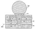
- FIG. 5is a cross-sectional view of the device of FIG. 3 following formation of a via plate and an under bump metallization in accordance with one embodiment of the present invention.
- FIG. 6is cross-sectional view of the device of FIG. 5 , illustrating the addition of a layer of material in the opening into the substrate in accordance with one embodiment of the present invention.
- FIG. 7is a cross-sectional view illustrating a protective layer disposed over the topography of the device of FIG. 6 in accordance with one embodiment of the present invention.
- FIG. 8is a cross-sectional view depicting the device of FIG. 7 after removal of a portion of the proactive layer in accordance with one embodiment of the present invention.
- FIG. 9is a cross-sectional view illustrating the device of FIG. 8 wherein a coating mechanism has disposed a fill material into a via of the device in accordance with one embodiment of the present invention.
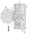
- FIG. 10is a cross-sectional view generally illustrating removal of the protective layer and addition of a bump to the device of FIG. 9 in accordance with one embodiment of the present invention.
- FIG. 11is a cross-sectional view generally illustrating backside topography on the device in FIG. 10 in accordance with one embodiment of the present invention.
- Embodiments of the present inventiongenerally relate to systems and methods for protecting existing features of a semiconductor device during formation of additional features on a substrate of the semiconductor device. Some embodiments of the present invention are directed to semiconductor devices that have been formed or partially formed in accordance with these systems and methods. Specifically, embodiments of the present invention relate to disposing a protective layer over a substrate to shield existing topography on a surface of the substrate from potentially damaging contact with equipment and/or materials utilized in coating operations.
- the protective layermay serve the purpose of planarizing the surface to facilitate spreading conductive materials (e.g., solder paste) or non-conductive materials with a spreading mechanism without causing damage to existing topography.
- the protective layermay also serve as a barrier between the existing topography and the spreading mechanism.
- the protective layermay seal the existing topography away from potentially harmful particulate matter in the spreading medium. Additionally, the planar nature of the protective layer may eliminate perturbations in the spreading medium due to the existing topography, which may cause distortions in the spreading equipment (e.g., distortion of a squeegee's geometry).
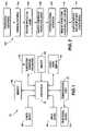
- FIG. 1is a block diagram of an electronic system containing integrated circuit devices that may employ embodiments of the present invention.
- the electronic device or systemwhich is generally indicated by the reference numeral 10 , may be any of a variety of types, such as a computer, digital camera, cellular phone, personal organizer, or the like.
- a processor 12such as a microprocessor, controls the operation of system functions and requests.
- an input device 14may be coupled to the processor 12 to receive input from a user.
- the input device 14may comprise a user interface and may include buttons, switches, a keyboard, a light pen, a mouse, a digitizer, a voice recognition system, or any of a number of other input devices.
- An audio/video display 16may also be coupled to the processor 12 to provide information to the user.
- the display 16may include an LCD display, a CRT display, or LEDs, for example.
- the system 10may include a power supply 18 , which may comprise a battery or batteries, a battery receptor, an AC power adapter, or a DC power adapter, for instance.
- the power supply 18may provide power to one or more components of the system 10 .
- An RF sub-system/baseband processor 20may be coupled to the processor 12 to provide wireless communication capability.
- the RF subsystem/baseband processor 20may include an antenna that is coupled to an RF receiver and to an RF transmitter (not shown).
- a communications port 22may be adapted to provide a communication interface between the electronic system 10 and a peripheral device 24 .
- the peripheral device 24may include a docking station, expansion bay, or other external component.
- the processor 12may be coupled to various types of memory devices to facilitate its operation.
- the processor 12may be connected to memory 26 , which may include volatile memory, non-volatile memory, or both.
- the volatile memory of memory 26may comprise a variety of memory types, such as static random access memory (“SRAM”), dynamic random access memory (“DRAM”), first, second, or third generation Double Data Rate memory (“DDR 1 ”, “DDR 2 ”, or “DDR 3 ”, respectively), or the like.
- the non-volatile memory of the memory 26may comprise various types of memory such as electrically programmable read only memory (“EPROM”) or flash memory, for example. Additionally, the non-volatile memory may include a high-capacity memory such as a tape or disk drive memory.
- the system 10may include multiple semiconductor devices.
- the system 10may also include an image sensor or imager 28 coupled to the processor 12 to provide digital imaging functionality.
- the imager 28may include a charge coupled device (CCD) sensor or a complementary metal oxide semiconductor (CMOS) sensor having an array of photoreceptors or pixel cells configured to be impacted by photons and to convert such impact into electrical current via the photoelectric effect. While the imager 28 may be coupled remotely from the processor 12 , such as by way of a circuit board, the imager 28 and processor 12 may instead be integrally formed, such as on a common substrate.
- CCDcharge coupled device
- CMOScomplementary metal oxide semiconductor
- a method 30 for manufacturing a semiconductor deviceis generally provided in FIG. 2 in accordance with one embodiment of the present invention.
- the method 30includes a number of steps 32 - 44 , which are described in greater detail below with respect to FIGS. 3-11 .
- the method 30includes a step 32 of providing a substrate and a step 34 of forming features or topography (e.g., a redistribution layer and a via) on and/or in the substrate, as generally discussed herein with respect to FIGS. 3-6 .
- the method 30also includes a step 36 of disposing a protective layer over the substrate and the added features, as is generally discussed below with reference to FIG. 7 .
- the method 30includes a step 38 of removing (e.g., etching) a portion of the protective layer to provide limited access to features of the substrate or the substrate itself, as discussed with respect to FIG. 8 .
- the method 30includes a step 40 of coating the protective layer with a spreader (e.g., a squeegee) such that any vias or openings in the substrate are filled with a spreading medium (e.g., solder or polymer), as discussed with respect to FIG. 9 .
- a spreadere.g., a squeegee
- the coating on the protective layer and the protective layer itselfmay be removed, as discussed with respect to FIGS. 10-11 .
- step 44the various layers and features on the substrate may constitute a functional device and may be coupled to other devices, as discussed with respect to FIGS. 10-11 . It should be noted that one or more of these steps of the method 30 may be performed in a reactor or processing chamber such that the environment in which the steps are performed may be regulated.
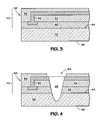
- FIG. 3illustrates a substrate 40 with various die features 42 disposed on one side of the substrate 40 .
- the substrate 40which may be made of silicon or another suitable material, includes a front side 44 and a backside 46 . It should be noted that the front side 44 may be designated as such because it is processed before the backside 46 .
- the present techniquemay be implemented as a wafer-level process, in which the substrate 40 is a semiconductor wafer having numerous die regions having various features formed thereon, such as an image sensor or processor, thus facilitating simultaneous mass production of such devices 40 .
- the substrate 40may be composed of other structures, such as an individual semiconductor die, in accordance with the present technique.
- the die features 42may include various layers of conductive, non-conductive, and semi-conductive material that are arranged to provide a function.
- the die features 42include a circuitry layer 48 and a redistribution layer 50 .
- the circuitry layer 42may include various sub-layers of different materials that have been arranged and manipulated to form integrated circuits for a processor, a memory device, a management circuit or the like.
- the redistribution layer 50includes multiple layers that have been arranged and manipulated to provide a conductive trace 52 that communicatively couples with the circuitry layer 48 to facilitate coupling with other devices and so forth.
- the conductive trace 52is formed from metal and is surrounded by non-conductive polymer layers 54 and 56 .
- Portions of the redistribution layer 50may be removed (e.g., etched) to provide openings for receiving material to form traces, pads, and so forth in accordance with present techniques.
- a groove 62has been etched into a portion of the top polymer layer 56 of the redistribution layer 50 to expose the conductive trace 52 .
- the groove 58will later be filled with conductive material to form another feature on the substrate 40 , such as a trace, a via plate or a pad.
- aligned portions of the redistribution layer 50 , the circuitry layer 48 , and the substrate 40have been removed or etched to provide an opening 60 for a via into the substrate 40 .
- Viasmay be included in a semiconductor device to perform any of various functions. For example, depending on the type of material disposed or grown in the via, the via may serve as a communicative coupling or to prevent stress build up in the substrate 40 during fabrication.
- the groove 58may be filled with a conductive material in accordance with present embodiments. Specifically, in the embodiment illustrated by FIG. 5 , the groove 58 has been filled with the conductive material to form a via plate 72 . Further, the via plate 72 is covered with an under bump metallization (UBM) 74 that is configured to receive a bump (e.g., a solder ball) or the like to facilitate directly or indirectly coupling with other devices (e.g., a memory or an imager). These features may be added through any of various procedures known in the art. Additionally, as illustrated in FIG. 6 , a layer of material 76 may be disposed along the interior walls of the opening 60 by any of various deposition processes to establish a via 80 .
- UBMunder bump metallization
- the layer of material 76may include any of various types of material (e.g., conductive material, insulation, or flexible material) depending on the desired function for the via 80 . If during such a deposition process, the layer of material 76 is disposed outside of the opening 60 (e.g., on a surface of the redistribution layer 50 ), it may be removed with an etching process or the like.
- materiale.g., conductive material, insulation, or flexible material
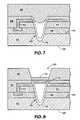
- FIG. 7illustrates a protective layer 90 disposed over the topography of the substrate 40 , as may be provided in step 36 of the method 30 in accordance with present embodiments.
- the protective layer 90may initially fill a portion of the via 80 , as illustrated in FIG. 7 .
- a portion of the protective layer 90 above the via 80may be removed to expose an opening 92 through the protective layer 90 and into the via 80 in accordance with present embodiments.
- any portion of the protective layer 90 that extended into the via 80will also be removed. It should be noted that having the protective layer 90 in place over the topography protectively seals the topography away from potentially harmful substances and shields the topography from spreading equipment that may be utilized to fill the via 80 with a desired material, as discussed in further detail below.
- the protective layer 90may be used essentially as a stencil in a coating operation, as indicated by step 40 in accordance with present embodiments.
- a fill material 100e.g., solder or polymer
- the coating device 102is a squeegee.
- the coating device 102may include any of various devices that pass over the protective layer 90 and press or inject the fill material 100 into openings (e.g., opening 92 ) therein.
- the coating device 102may include a print head, a pressurized head, or the like.
- the protective layer 90may be planarized to facilitate passage of the coating device 102 over the protective layer 90 with little resistance.
- planarization of the protective layer 90may be achieved by wearing down inconsistencies on the outer portion of the protective layer 90 with a wet polish pad or the like. This may prevent the creation of artifacts in the fill material 100 resulting from distortion of the coating device 102 , which could be caused by substantially uneven contact between the coating device 102 and the protective layer 90 .
- a squeegeemay flex or bend while passing over the protective layer 90 if one side of the squeegee passes over a high point of the protective layer 90 while another side passes over a low point. Such distortion may cause a disruption in the even distribution of the fill material 100 .
- the protective layer 90may be removed in accordance with an embodiment of the present invention. For example, this may be achieved with an etching process that utilizes a specific etching chemical for the specific type of material used to form the protective layer 90 . Similarly, the portion of the fill material 100 residing in the opening 92 in the protective layer 90 may be removed by etching. For example, FIG. 10 illustrates the substrate 40 and its topography after removal of the protective layer 90 and the excess fill material 100 that extended into the opening 92 in the protective layer 90 . Once the protective layer 90 is removed, the UMB 74 is exposed and a contact bump 200 may be coupled to the surface of the UBM 74 .
- the contact bumpmay be formed of any suitable, electrically conductive material, such as solder.
- the contact bump 200facilitates direct coupling to other circuitry.
- the contact bump 200may enable direct coupling with a socket in a circuit board or allow electrical communication between features of the substrate 40 and external electronic devices, as set forth in step 44 of method 30 in accordance with present embodiments.
- the various layers and features on the substrate 40may eventually constitute a functional device 300 (e.g., a memory or processor). Indeed, some functionality may be provided on the backside 46 of the device 300 .
- the back side 46 of the substrate 40may be modified to include backside topography 302 . This modification may include etching or grinding away a portion of the substrate 40 and disposing backside topography 302 thereon.
- the backside topography 302may be formed through any suitable combination of processes. For instance, in one embodiment, portions of the backside topography 302 are spun-on to the substrate 40 and patterned to form particular features.
- patterningmay include applying a photoresist layer to a passivation layer, then exposing and developing the photoresist layer to form trenches that can be filled with conductive material to define vias, and so forth.
- forming the backside topographymay include grinding and/or polishing processes designed to wear away layers and expose previously disposed features. It should be noted that during backside processing, a protective layer similar to that used on the front side may also be employed.
Landscapes
- Engineering & Computer Science (AREA)
- Computer Hardware Design (AREA)
- Microelectronics & Electronic Packaging (AREA)
- Power Engineering (AREA)
- Physics & Mathematics (AREA)
- Condensed Matter Physics & Semiconductors (AREA)
- General Physics & Mathematics (AREA)
- Manufacturing & Machinery (AREA)
- Internal Circuitry In Semiconductor Integrated Circuit Devices (AREA)
Abstract
Description
- 1. Field of the Invention
- Embodiments of the present invention relate generally to the field of semiconductor devices. More particularly, embodiments of the present invention relate to using a protective layer to provide features of a semiconductor device.
- 2. Description of the Related Art
- Microprocessor-controlled circuits are used in a wide variety of applications. Such applications include personal computers, cellular phones, digital cameras, control systems, and a host of other consumer products. A personal computer, digital camera, or the like, generally includes various components, such as microprocessors, that handle different functions for the system. By combining these components, various consumer products and systems may be designed to meet specific needs. Microprocessors are essentially generic devices that perform specific functions under the control of software programs. These software programs are generally stored in one or more memory devices that are coupled to the microprocessor and/or other peripherals.
- Electronic components such as microprocessors and memory devices often include numerous integrated circuits manufactured on a semiconductor substrate. The various structures or features of these integrated circuits may be fabricated on a substrate through a variety of manufacturing processes known in the art, including layering, doping, and patterning. It is often desirable to efficiently utilize available space on a substrate by providing planar layers that are essentially stacked on the substrate. The planar layers expand the substrate in a vertical direction relative to the plane of the substrate, thus utilizing the surface area of the substrate more efficiently. Various features or structures may be fabricated in, on, and through these layers. To electrically couple elements formed in different layers, vias may be employed. A via may be defined as a vertical opening filled with conducting material that electrically connects circuits or multiple layers of a device to each other and/or to a substrate. A via may also be filled with non-conductive material that performs various functions, such as preventing stress build up in the substrate during wafer fabrication.
- Traditional procedures for fabricating die features, such as disposing conductive or non-conductive material in holes to form vias, often result in damaging existing topography (e.g., traces and pads) on or near the outermost surface of the substrate. For example, in techniques that utilize stencils to fabricate substrate features, movement of the stencil relative to the substrate may cause harmful contact between the stencil and certain topographic features on the surface of the substrate. Additionally, the material being used to form the substrate features (e.g., material being disposed in a via) may include particulate matter that can harm existing substrate topography, and traditional techniques for disposing such materials on the substrate may facilitate contact between the surface of the substrate and this harmful particulate matter. For example, certain gels that are disposed directly adjacent a substrate surface during screen printing processes may readily receive the particulate matter, thus allowing contact between the substrate surface and the particulate matter. Similarly, the particulate matter may get between a stencil and the substrate in procedures that employ stencils. Accordingly, it is now recognized that it is desirable to provide a system and method of providing semiconductor device features that limit the potential damage associated with providing such features using traditional techniques.
FIG. 1 illustrates a block diagram of a processor-based device in accordance with an embodiment of the present invention.FIG. 2 is a flow diagram of a method related to the manufacture of a device in accordance with an embodiment of the present invention.FIG. 3 is a cross-sectional view of a device including a substrate with circuitry and a redistribution layer disposed thereon in accordance with a step of one embodiment of the present invention.FIG. 4 is a cross-sectional view of the device ofFIG. 3 , wherein an opening has been provided into the substrate in accordance with a step of one embodiment of the present invention.FIG. 5 is a cross-sectional view of the device ofFIG. 3 following formation of a via plate and an under bump metallization in accordance with one embodiment of the present invention.FIG. 6 is cross-sectional view of the device ofFIG. 5 , illustrating the addition of a layer of material in the opening into the substrate in accordance with one embodiment of the present invention.FIG. 7 is a cross-sectional view illustrating a protective layer disposed over the topography of the device ofFIG. 6 in accordance with one embodiment of the present invention.FIG. 8 is a cross-sectional view depicting the device ofFIG. 7 after removal of a portion of the proactive layer in accordance with one embodiment of the present invention.FIG. 9 is a cross-sectional view illustrating the device ofFIG. 8 wherein a coating mechanism has disposed a fill material into a via of the device in accordance with one embodiment of the present invention.FIG. 10 is a cross-sectional view generally illustrating removal of the protective layer and addition of a bump to the device ofFIG. 9 in accordance with one embodiment of the present invention.FIG. 11 is a cross-sectional view generally illustrating backside topography on the device inFIG. 10 in accordance with one embodiment of the present invention.- Embodiments of the present invention generally relate to systems and methods for protecting existing features of a semiconductor device during formation of additional features on a substrate of the semiconductor device. Some embodiments of the present invention are directed to semiconductor devices that have been formed or partially formed in accordance with these systems and methods. Specifically, embodiments of the present invention relate to disposing a protective layer over a substrate to shield existing topography on a surface of the substrate from potentially damaging contact with equipment and/or materials utilized in coating operations. For example, the protective layer may serve the purpose of planarizing the surface to facilitate spreading conductive materials (e.g., solder paste) or non-conductive materials with a spreading mechanism without causing damage to existing topography. The protective layer may also serve as a barrier between the existing topography and the spreading mechanism. Further, the protective layer may seal the existing topography away from potentially harmful particulate matter in the spreading medium. Additionally, the planar nature of the protective layer may eliminate perturbations in the spreading medium due to the existing topography, which may cause distortions in the spreading equipment (e.g., distortion of a squeegee's geometry).
- Turning now to the drawings,
FIG. 1 is a block diagram of an electronic system containing integrated circuit devices that may employ embodiments of the present invention. The electronic device or system, which is generally indicated by thereference numeral 10, may be any of a variety of types, such as a computer, digital camera, cellular phone, personal organizer, or the like. In a typical processor-based device, aprocessor 12, such as a microprocessor, controls the operation of system functions and requests. - Various devices may be coupled to the
processor 12 depending on the functions that thesystem 10 performs. For example, aninput device 14 may be coupled to theprocessor 12 to receive input from a user. Theinput device 14 may comprise a user interface and may include buttons, switches, a keyboard, a light pen, a mouse, a digitizer, a voice recognition system, or any of a number of other input devices. An audio/video display 16 may also be coupled to theprocessor 12 to provide information to the user. Thedisplay 16 may include an LCD display, a CRT display, or LEDs, for example. Further, thesystem 10 may include apower supply 18, which may comprise a battery or batteries, a battery receptor, an AC power adapter, or a DC power adapter, for instance. Thepower supply 18 may provide power to one or more components of thesystem 10. - An RF sub-system/
baseband processor 20 may be coupled to theprocessor 12 to provide wireless communication capability. The RF subsystem/baseband processor 20 may include an antenna that is coupled to an RF receiver and to an RF transmitter (not shown). Furthermore, acommunications port 22 may be adapted to provide a communication interface between theelectronic system 10 and aperipheral device 24. Theperipheral device 24 may include a docking station, expansion bay, or other external component. - The
processor 12 may be coupled to various types of memory devices to facilitate its operation. For example, theprocessor 12 may be connected tomemory 26, which may include volatile memory, non-volatile memory, or both. The volatile memory ofmemory 26 may comprise a variety of memory types, such as static random access memory (“SRAM”), dynamic random access memory (“DRAM”), first, second, or third generation Double Data Rate memory (“DDR1”, “DDR2”, or “DDR3”, respectively), or the like. The non-volatile memory of thememory 26 may comprise various types of memory such as electrically programmable read only memory (“EPROM”) or flash memory, for example. Additionally, the non-volatile memory may include a high-capacity memory such as a tape or disk drive memory. - The
system 10 may include multiple semiconductor devices. For example, in addition to theprocessor 12 and thememory 26, thesystem 10 may also include an image sensor orimager 28 coupled to theprocessor 12 to provide digital imaging functionality. Theimager 28 may include a charge coupled device (CCD) sensor or a complementary metal oxide semiconductor (CMOS) sensor having an array of photoreceptors or pixel cells configured to be impacted by photons and to convert such impact into electrical current via the photoelectric effect. While theimager 28 may be coupled remotely from theprocessor 12, such as by way of a circuit board, theimager 28 andprocessor 12 may instead be integrally formed, such as on a common substrate. - A
method 30 for manufacturing a semiconductor device, such as theprocessor 12, thememory 26 and/or theimager 28, is generally provided inFIG. 2 in accordance with one embodiment of the present invention. Particularly, themethod 30 includes a number of steps32-44, which are described in greater detail below with respect toFIGS. 3-11 . For instance, themethod 30 includes astep 32 of providing a substrate and astep 34 of forming features or topography (e.g., a redistribution layer and a via) on and/or in the substrate, as generally discussed herein with respect toFIGS. 3-6 . Themethod 30 also includes astep 36 of disposing a protective layer over the substrate and the added features, as is generally discussed below with reference toFIG. 7 . Additionally, themethod 30 includes astep 38 of removing (e.g., etching) a portion of the protective layer to provide limited access to features of the substrate or the substrate itself, as discussed with respect toFIG. 8 . Further, themethod 30 includes astep 40 of coating the protective layer with a spreader (e.g., a squeegee) such that any vias or openings in the substrate are filled with a spreading medium (e.g., solder or polymer), as discussed with respect toFIG. 9 . Next, instep 42, the coating on the protective layer and the protective layer itself may be removed, as discussed with respect toFIGS. 10-11 . Finally, instep 44, the various layers and features on the substrate may constitute a functional device and may be coupled to other devices, as discussed with respect toFIGS. 10-11 . It should be noted that one or more of these steps of themethod 30 may be performed in a reactor or processing chamber such that the environment in which the steps are performed may be regulated. - As may be provided in
steps method 30 in accordance with an embodiment of the present invention,FIG. 3 illustrates asubstrate 40 with various die features42 disposed on one side of thesubstrate 40. Thesubstrate 40, which may be made of silicon or another suitable material, includes afront side 44 and abackside 46. It should be noted that thefront side 44 may be designated as such because it is processed before thebackside 46. For the sake of efficiency, the present technique may be implemented as a wafer-level process, in which thesubstrate 40 is a semiconductor wafer having numerous die regions having various features formed thereon, such as an image sensor or processor, thus facilitating simultaneous mass production ofsuch devices 40. In other embodiments, however, thesubstrate 40 may be composed of other structures, such as an individual semiconductor die, in accordance with the present technique. - The die features42 may include various layers of conductive, non-conductive, and semi-conductive material that are arranged to provide a function. For example, in the illustrated embodiment, the die features42 include a
circuitry layer 48 and aredistribution layer 50. Thecircuitry layer 42 may include various sub-layers of different materials that have been arranged and manipulated to form integrated circuits for a processor, a memory device, a management circuit or the like. Similarly, theredistribution layer 50 includes multiple layers that have been arranged and manipulated to provide aconductive trace 52 that communicatively couples with thecircuitry layer 48 to facilitate coupling with other devices and so forth. Specifically, in the illustrated embodiment, theconductive trace 52 is formed from metal and is surrounded by non-conductive polymer layers54 and56. - Portions of the
redistribution layer 50 may be removed (e.g., etched) to provide openings for receiving material to form traces, pads, and so forth in accordance with present techniques. For example, in the embodiment illustrated inFIG. 4 , a groove62 has been etched into a portion of thetop polymer layer 56 of theredistribution layer 50 to expose theconductive trace 52. In one embodiment, thegroove 58 will later be filled with conductive material to form another feature on thesubstrate 40, such as a trace, a via plate or a pad. Additionally, in the illustrated embodiment, aligned portions of theredistribution layer 50, thecircuitry layer 48, and thesubstrate 40 have been removed or etched to provide anopening 60 for a via into thesubstrate 40. Vias may be included in a semiconductor device to perform any of various functions. For example, depending on the type of material disposed or grown in the via, the via may serve as a communicative coupling or to prevent stress build up in thesubstrate 40 during fabrication. - As illustrated in
FIG. 5 , thegroove 58 may be filled with a conductive material in accordance with present embodiments. Specifically, in the embodiment illustrated byFIG. 5 , thegroove 58 has been filled with the conductive material to form a viaplate 72. Further, the viaplate 72 is covered with an under bump metallization (UBM)74 that is configured to receive a bump (e.g., a solder ball) or the like to facilitate directly or indirectly coupling with other devices (e.g., a memory or an imager). These features may be added through any of various procedures known in the art. Additionally, as illustrated inFIG. 6 , a layer ofmaterial 76 may be disposed along the interior walls of theopening 60 by any of various deposition processes to establish a via80. The layer ofmaterial 76 may include any of various types of material (e.g., conductive material, insulation, or flexible material) depending on the desired function for the via80. If during such a deposition process, the layer ofmaterial 76 is disposed outside of the opening60 (e.g., on a surface of the redistribution layer50), it may be removed with an etching process or the like. - All of the added features on the
substrate 40, such as theredistribution layer 50, the via80, the viaplate 72, theUBM 74 and so forth may be generally referred to as topography.FIG. 7 illustrates aprotective layer 90 disposed over the topography of thesubstrate 40, as may be provided instep 36 of themethod 30 in accordance with present embodiments. Theprotective layer 90 may initially fill a portion of the via80, as illustrated inFIG. 7 . However, as may be provided instep 38 and as illustrated inFIG. 8 , a portion of theprotective layer 90 above the via80 may be removed to expose anopening 92 through theprotective layer 90 and into the via80 in accordance with present embodiments. During this removal process (e.g., etching), any portion of theprotective layer 90 that extended into the via80 will also be removed. It should be noted that having theprotective layer 90 in place over the topography protectively seals the topography away from potentially harmful substances and shields the topography from spreading equipment that may be utilized to fill the via80 with a desired material, as discussed in further detail below. - As illustrated in
FIG. 9 , once theprotective layer 90 is in place over the topography of thesubstrate 40, it may be used essentially as a stencil in a coating operation, as indicated bystep 40 in accordance with present embodiments. Specifically, as illustrated inFIG. 9 a fill material100 (e.g., solder or polymer) may be pushed into the via80 through theopening 92 in theprotective layer 90 by acoating device 102. In the illustrated embodiment, thecoating device 102 is a squeegee. However, in other embodiments thecoating device 102 may include any of various devices that pass over theprotective layer 90 and press or inject thefill material 100 into openings (e.g., opening92) therein. For example, in some embodiments, thecoating device 102 may include a print head, a pressurized head, or the like. - It should be noted that prior to moving the
coating device 102 across theprotective layer 90, theprotective layer 90 may be planarized to facilitate passage of thecoating device 102 over theprotective layer 90 with little resistance. For example, planarization of theprotective layer 90 may be achieved by wearing down inconsistencies on the outer portion of theprotective layer 90 with a wet polish pad or the like. This may prevent the creation of artifacts in thefill material 100 resulting from distortion of thecoating device 102, which could be caused by substantially uneven contact between thecoating device 102 and theprotective layer 90. For example, a squeegee may flex or bend while passing over theprotective layer 90 if one side of the squeegee passes over a high point of theprotective layer 90 while another side passes over a low point. Such distortion may cause a disruption in the even distribution of thefill material 100. - As set forth in
step 42 ofmethod 30, once the via80 has been filled with thefill material 100, theprotective layer 90 may be removed in accordance with an embodiment of the present invention. For example, this may be achieved with an etching process that utilizes a specific etching chemical for the specific type of material used to form theprotective layer 90. Similarly, the portion of thefill material 100 residing in theopening 92 in theprotective layer 90 may be removed by etching. For example,FIG. 10 illustrates thesubstrate 40 and its topography after removal of theprotective layer 90 and theexcess fill material 100 that extended into theopening 92 in theprotective layer 90. Once theprotective layer 90 is removed, theUMB 74 is exposed and acontact bump 200 may be coupled to the surface of theUBM 74. The contact bump may be formed of any suitable, electrically conductive material, such as solder. Notably, thecontact bump 200 facilitates direct coupling to other circuitry. For example, in one embodiment, thecontact bump 200 may enable direct coupling with a socket in a circuit board or allow electrical communication between features of thesubstrate 40 and external electronic devices, as set forth instep 44 ofmethod 30 in accordance with present embodiments. - The various layers and features on the
substrate 40 may eventually constitute a functional device300 (e.g., a memory or processor). Indeed, some functionality may be provided on thebackside 46 of thedevice 300. For example, as illustrated inFIG. 11 , theback side 46 of thesubstrate 40 may be modified to includebackside topography 302. This modification may include etching or grinding away a portion of thesubstrate 40 and disposingbackside topography 302 thereon. As with the provision of the features of the front side, thebackside topography 302 may be formed through any suitable combination of processes. For instance, in one embodiment, portions of thebackside topography 302 are spun-on to thesubstrate 40 and patterned to form particular features. For example, in one embodiment, patterning may include applying a photoresist layer to a passivation layer, then exposing and developing the photoresist layer to form trenches that can be filled with conductive material to define vias, and so forth. Further, in other embodiments, forming the backside topography may include grinding and/or polishing processes designed to wear away layers and expose previously disposed features. It should be noted that during backside processing, a protective layer similar to that used on the front side may also be employed. - While the invention may be susceptible to various modifications and alternative forms, specific embodiments have been shown by way of example in the drawings and have been described in detail herein. However, it should be understood that the invention is not intended to be limited to the particular forms disclosed. Rather, the invention is to cover all modifications, equivalents, and alternatives falling within the spirit and scope of the invention as defined by the following appended claims.
Claims (24)
Priority Applications (1)
| Application Number | Priority Date | Filing Date | Title |
|---|---|---|---|
| US11/888,122US20090032964A1 (en) | 2007-07-31 | 2007-07-31 | System and method for providing semiconductor device features using a protective layer |
Applications Claiming Priority (1)
| Application Number | Priority Date | Filing Date | Title |
|---|---|---|---|
| US11/888,122US20090032964A1 (en) | 2007-07-31 | 2007-07-31 | System and method for providing semiconductor device features using a protective layer |
Publications (1)
| Publication Number | Publication Date |
|---|---|
| US20090032964A1true US20090032964A1 (en) | 2009-02-05 |
Family
ID=40337352
Family Applications (1)
| Application Number | Title | Priority Date | Filing Date |
|---|---|---|---|
| US11/888,122AbandonedUS20090032964A1 (en) | 2007-07-31 | 2007-07-31 | System and method for providing semiconductor device features using a protective layer |
Country Status (1)
| Country | Link |
|---|---|
| US (1) | US20090032964A1 (en) |
Cited By (6)
| Publication number | Priority date | Publication date | Assignee | Title |
|---|---|---|---|---|
| US20090026566A1 (en)* | 2007-07-27 | 2009-01-29 | Micron Technology, Inc. | Semiconductor device having backside redistribution layers and method for fabricating the same |
| US20090065927A1 (en)* | 2007-09-06 | 2009-03-12 | Infineon Technologies Ag | Semiconductor Device and Methods of Manufacturing Semiconductor Devices |
| US20110052979A1 (en)* | 2009-08-28 | 2011-03-03 | Stmicroelectronics (Tours) Sas | Method of direct encapsulation of a thin-film lithium-ion type battery on the substrate |
| KR101142337B1 (en) | 2010-05-07 | 2012-05-17 | 에스케이하이닉스 주식회사 | Semiconductor chip and method of manufacturing thereof and stack package using the semiconductor chip |
| US20140145345A1 (en)* | 2012-11-27 | 2014-05-29 | Infineon Technologies Ag | Method of forming a semiconductor structure, and a semiconductor structure |
| US11088068B2 (en)* | 2019-04-29 | 2021-08-10 | Taiwan Semiconductor Manufacturing Company, Ltd. | Semiconductor packages and methods of manufacturing the same |
Citations (35)
| Publication number | Priority date | Publication date | Assignee | Title |
|---|---|---|---|---|
| US4888300A (en)* | 1985-11-07 | 1989-12-19 | Fairchild Camera And Instrument Corporation | Submerged wall isolation of silicon islands |
| US5166097A (en)* | 1990-11-26 | 1992-11-24 | The Boeing Company | Silicon wafers containing conductive feedthroughs |
| US5461003A (en)* | 1994-05-27 | 1995-10-24 | Texas Instruments Incorporated | Multilevel interconnect structure with air gaps formed between metal leads |
| US5652557A (en)* | 1994-10-19 | 1997-07-29 | Mitsubishi Denki Kabushiki Kaisha | Transmission lines and fabricating method thereof |
| US5920790A (en)* | 1997-08-29 | 1999-07-06 | Motorola, Inc. | Method of forming a semiconductor device having dual inlaid structure |
| US5994763A (en)* | 1997-06-30 | 1999-11-30 | Oki Electric Industry Co., Ltd. | Wiring structure for semiconductor element and method for forming the same |
| US6022797A (en)* | 1996-11-29 | 2000-02-08 | Hitachi, Ltd. | Method of manufacturing through holes in a semiconductor device |
| US6072210A (en)* | 1998-12-24 | 2000-06-06 | Lucent Technologies Inc. | Integrate DRAM cell having a DRAM capacitor and a transistor |
| US6159840A (en)* | 1999-11-12 | 2000-12-12 | United Semiconductor Corp. | Fabrication method for a dual damascene comprising an air-gap |
| US6268283B1 (en)* | 1999-01-06 | 2001-07-31 | United Microelectronics Corp. | Method for forming dual damascene structure |
| US20010012689A1 (en)* | 1998-12-03 | 2001-08-09 | Uzodinma Okoroanyanwu | Interconnect structure with silicon containing alicyclic polymers and low-k dieletric materials and method of making same with single and dual damascene techniques |
| US6437451B2 (en)* | 1999-03-22 | 2002-08-20 | Micron Technology, Inc. | Test interconnect for semiconductor components having bumped and planar contacts |
| US6555921B2 (en)* | 1999-07-12 | 2003-04-29 | Samsung Electronics Co., Ltd. | Semiconductor package |
| US6693358B2 (en)* | 2000-10-23 | 2004-02-17 | Matsushita Electric Industrial Co., Ltd. | Semiconductor chip, wiring board and manufacturing process thereof as well as semiconductor device |
| US20040056345A1 (en)* | 2002-09-25 | 2004-03-25 | Gilleo Kenneth B. | Via interconnect forming process and electronic component product thereof |
| US20040166659A1 (en)* | 1998-12-21 | 2004-08-26 | Megic Corporation | Top layers of metal for high performance IC's |
| US6815329B2 (en)* | 2000-02-08 | 2004-11-09 | International Business Machines Corporation | Multilayer interconnect structure containing air gaps and method for making |
| US6866972B2 (en)* | 2002-05-15 | 2005-03-15 | Nec Lcd Technologies, Ltd. | Color layer forming method |
| US20050158985A1 (en)* | 2002-12-16 | 2005-07-21 | Shyng-Tsong Chen | Copper recess process with application to selective capping and electroless plating |
| US6952054B2 (en)* | 1997-12-18 | 2005-10-04 | Micron Technology, Inc. | Semiconductor package having interconnect with conductive members |
| US20050282378A1 (en)* | 2004-06-22 | 2005-12-22 | Akira Fukunaga | Interconnects forming method and interconnects forming apparatus |
| US20060003579A1 (en)* | 2004-06-30 | 2006-01-05 | Sir Jiun H | Interconnects with direct metalization and conductive polymer |
| US20060001439A1 (en)* | 1996-04-01 | 2006-01-05 | Salman Akram | Semiconductor test interconnect with variable flexure contacts having polymer material |
| US6994949B2 (en)* | 2001-06-30 | 2006-02-07 | Hynix Semiconductor Inc. | Method for manufacturing multi-level interconnections with dual damascene process |
| US20060046468A1 (en)* | 2004-08-31 | 2006-03-02 | Salman Akram | Through-substrate interconnect fabrication methods and resulting structures and assemblies |
| US20060043599A1 (en)* | 2004-09-02 | 2006-03-02 | Salman Akram | Through-wafer interconnects for photoimager and memory wafers |
| US20060105558A1 (en)* | 2004-11-18 | 2006-05-18 | Harry Chuang | Inter-metal dielectric scheme for semiconductors |
| US20060160274A1 (en)* | 2003-09-19 | 2006-07-20 | Larson Charles E | Methods relating to forming interconnects |
| US20060252225A1 (en)* | 2005-05-05 | 2006-11-09 | Gambee Christopher J | Method to create a metal pattern using a damascene-like process and associated structures |
| US20060292877A1 (en)* | 2005-06-28 | 2006-12-28 | Lake Rickie C | Semiconductor substrates including vias of nonuniform cross section, methods of forming and associated structures |
| US20080171432A1 (en)* | 2007-01-16 | 2008-07-17 | International Business Machines Corporation | Circuit Structure with Low Dielectric Constant Regions and Method of Forming Same |
| US20080185728A1 (en)* | 2007-02-02 | 2008-08-07 | International Business Machines Corporation | Microelectronic Circuit Structure With Layered Low Dielectric Constant Regions And Method Of Forming Same |
| US7414314B2 (en)* | 2004-01-14 | 2008-08-19 | Oki Electric Industry Co., Ltd. | Semiconductor device and manufacturing method thereof |
| US20080237868A1 (en)* | 2007-03-29 | 2008-10-02 | International Business Machines Corporation | Method and structure for ultra narrow crack stop for multilevel semiconductor device |
| US20090026566A1 (en)* | 2007-07-27 | 2009-01-29 | Micron Technology, Inc. | Semiconductor device having backside redistribution layers and method for fabricating the same |
- 2007
- 2007-07-31USUS11/888,122patent/US20090032964A1/ennot_activeAbandoned
Patent Citations (36)
| Publication number | Priority date | Publication date | Assignee | Title |
|---|---|---|---|---|
| US4888300A (en)* | 1985-11-07 | 1989-12-19 | Fairchild Camera And Instrument Corporation | Submerged wall isolation of silicon islands |
| US5166097A (en)* | 1990-11-26 | 1992-11-24 | The Boeing Company | Silicon wafers containing conductive feedthroughs |
| US5461003A (en)* | 1994-05-27 | 1995-10-24 | Texas Instruments Incorporated | Multilevel interconnect structure with air gaps formed between metal leads |
| US5652557A (en)* | 1994-10-19 | 1997-07-29 | Mitsubishi Denki Kabushiki Kaisha | Transmission lines and fabricating method thereof |
| US20060001439A1 (en)* | 1996-04-01 | 2006-01-05 | Salman Akram | Semiconductor test interconnect with variable flexure contacts having polymer material |
| US6022797A (en)* | 1996-11-29 | 2000-02-08 | Hitachi, Ltd. | Method of manufacturing through holes in a semiconductor device |
| US5994763A (en)* | 1997-06-30 | 1999-11-30 | Oki Electric Industry Co., Ltd. | Wiring structure for semiconductor element and method for forming the same |
| US5920790A (en)* | 1997-08-29 | 1999-07-06 | Motorola, Inc. | Method of forming a semiconductor device having dual inlaid structure |
| US6952054B2 (en)* | 1997-12-18 | 2005-10-04 | Micron Technology, Inc. | Semiconductor package having interconnect with conductive members |
| US20010012689A1 (en)* | 1998-12-03 | 2001-08-09 | Uzodinma Okoroanyanwu | Interconnect structure with silicon containing alicyclic polymers and low-k dieletric materials and method of making same with single and dual damascene techniques |
| US6475904B2 (en)* | 1998-12-03 | 2002-11-05 | Advanced Micro Devices, Inc. | Interconnect structure with silicon containing alicyclic polymers and low-k dielectric materials and method of making same with single and dual damascene techniques |
| US20040166659A1 (en)* | 1998-12-21 | 2004-08-26 | Megic Corporation | Top layers of metal for high performance IC's |
| US6072210A (en)* | 1998-12-24 | 2000-06-06 | Lucent Technologies Inc. | Integrate DRAM cell having a DRAM capacitor and a transistor |
| US6268283B1 (en)* | 1999-01-06 | 2001-07-31 | United Microelectronics Corp. | Method for forming dual damascene structure |
| US6437451B2 (en)* | 1999-03-22 | 2002-08-20 | Micron Technology, Inc. | Test interconnect for semiconductor components having bumped and planar contacts |
| US6555921B2 (en)* | 1999-07-12 | 2003-04-29 | Samsung Electronics Co., Ltd. | Semiconductor package |
| US6159840A (en)* | 1999-11-12 | 2000-12-12 | United Semiconductor Corp. | Fabrication method for a dual damascene comprising an air-gap |
| US6815329B2 (en)* | 2000-02-08 | 2004-11-09 | International Business Machines Corporation | Multilayer interconnect structure containing air gaps and method for making |
| US6693358B2 (en)* | 2000-10-23 | 2004-02-17 | Matsushita Electric Industrial Co., Ltd. | Semiconductor chip, wiring board and manufacturing process thereof as well as semiconductor device |
| US6994949B2 (en)* | 2001-06-30 | 2006-02-07 | Hynix Semiconductor Inc. | Method for manufacturing multi-level interconnections with dual damascene process |
| US6866972B2 (en)* | 2002-05-15 | 2005-03-15 | Nec Lcd Technologies, Ltd. | Color layer forming method |
| US20040056345A1 (en)* | 2002-09-25 | 2004-03-25 | Gilleo Kenneth B. | Via interconnect forming process and electronic component product thereof |
| US20050158985A1 (en)* | 2002-12-16 | 2005-07-21 | Shyng-Tsong Chen | Copper recess process with application to selective capping and electroless plating |
| US20060160274A1 (en)* | 2003-09-19 | 2006-07-20 | Larson Charles E | Methods relating to forming interconnects |
| US7414314B2 (en)* | 2004-01-14 | 2008-08-19 | Oki Electric Industry Co., Ltd. | Semiconductor device and manufacturing method thereof |
| US20050282378A1 (en)* | 2004-06-22 | 2005-12-22 | Akira Fukunaga | Interconnects forming method and interconnects forming apparatus |
| US20060003579A1 (en)* | 2004-06-30 | 2006-01-05 | Sir Jiun H | Interconnects with direct metalization and conductive polymer |
| US20060046468A1 (en)* | 2004-08-31 | 2006-03-02 | Salman Akram | Through-substrate interconnect fabrication methods and resulting structures and assemblies |
| US20060043599A1 (en)* | 2004-09-02 | 2006-03-02 | Salman Akram | Through-wafer interconnects for photoimager and memory wafers |
| US20060105558A1 (en)* | 2004-11-18 | 2006-05-18 | Harry Chuang | Inter-metal dielectric scheme for semiconductors |
| US20060252225A1 (en)* | 2005-05-05 | 2006-11-09 | Gambee Christopher J | Method to create a metal pattern using a damascene-like process and associated structures |
| US20060292877A1 (en)* | 2005-06-28 | 2006-12-28 | Lake Rickie C | Semiconductor substrates including vias of nonuniform cross section, methods of forming and associated structures |
| US20080171432A1 (en)* | 2007-01-16 | 2008-07-17 | International Business Machines Corporation | Circuit Structure with Low Dielectric Constant Regions and Method of Forming Same |
| US20080185728A1 (en)* | 2007-02-02 | 2008-08-07 | International Business Machines Corporation | Microelectronic Circuit Structure With Layered Low Dielectric Constant Regions And Method Of Forming Same |
| US20080237868A1 (en)* | 2007-03-29 | 2008-10-02 | International Business Machines Corporation | Method and structure for ultra narrow crack stop for multilevel semiconductor device |
| US20090026566A1 (en)* | 2007-07-27 | 2009-01-29 | Micron Technology, Inc. | Semiconductor device having backside redistribution layers and method for fabricating the same |
Cited By (12)
| Publication number | Priority date | Publication date | Assignee | Title |
|---|---|---|---|---|
| US20090026566A1 (en)* | 2007-07-27 | 2009-01-29 | Micron Technology, Inc. | Semiconductor device having backside redistribution layers and method for fabricating the same |
| US7932179B2 (en) | 2007-07-27 | 2011-04-26 | Micron Technology, Inc. | Method for fabricating semiconductor device having backside redistribution layers |
| US20110169122A1 (en)* | 2007-07-27 | 2011-07-14 | Micron Technology, Inc. | Semiconductor device having backside redistribution layers and method for fabricating the same |
| US8395242B2 (en) | 2007-07-27 | 2013-03-12 | Micron Technology, Inc. | Semiconductor device having backside redistribution layers |
| US8963292B2 (en) | 2007-07-27 | 2015-02-24 | Micron Technology, Inc. | Semiconductor device having backside redistribution layers and method for fabricating the same |
| US20090065927A1 (en)* | 2007-09-06 | 2009-03-12 | Infineon Technologies Ag | Semiconductor Device and Methods of Manufacturing Semiconductor Devices |
| US7868446B2 (en)* | 2007-09-06 | 2011-01-11 | Infineon Technologies Ag | Semiconductor device and methods of manufacturing semiconductor devices |
| US20110052979A1 (en)* | 2009-08-28 | 2011-03-03 | Stmicroelectronics (Tours) Sas | Method of direct encapsulation of a thin-film lithium-ion type battery on the substrate |
| US8840686B2 (en)* | 2009-08-28 | 2014-09-23 | Stmicroelectronics (Tours) Sas | Method of direct encapsulation of a thin-film lithium-ion type battery on the substrate |
| KR101142337B1 (en) | 2010-05-07 | 2012-05-17 | 에스케이하이닉스 주식회사 | Semiconductor chip and method of manufacturing thereof and stack package using the semiconductor chip |
| US20140145345A1 (en)* | 2012-11-27 | 2014-05-29 | Infineon Technologies Ag | Method of forming a semiconductor structure, and a semiconductor structure |
| US11088068B2 (en)* | 2019-04-29 | 2021-08-10 | Taiwan Semiconductor Manufacturing Company, Ltd. | Semiconductor packages and methods of manufacturing the same |
Similar Documents
| Publication | Publication Date | Title |
|---|---|---|
| US7932179B2 (en) | Method for fabricating semiconductor device having backside redistribution layers | |
| US9136259B2 (en) | Method of creating alignment/centering guides for small diameter, high density through-wafer via die stacking | |
| US20090032964A1 (en) | System and method for providing semiconductor device features using a protective layer | |
| US10636700B2 (en) | Metal via processing schemes with via critical dimension (CD) control for back end of line (BEOL) interconnects and the resulting structures | |
| US10643888B2 (en) | Overlay marks, methods of forming the same, and methods of fabricating semiconductor devices using the same | |
| CN102299086A (en) | Semiconductor package and producing method and system thereof | |
| US8273635B2 (en) | Semiconductor fabrication method and system | |
| CN105321914A (en) | Chip and chip-stacked package using the same | |
| US11404390B2 (en) | Semiconductor device assembly with sacrificial pillars and methods of manufacturing sacrificial pillars | |
| US8486787B2 (en) | Method of fabricating semiconductor device | |
| TW200910580A (en) | CMOS image sensor package and method thereof | |
| CN109711230B (en) | Semiconductor fingerprint sensor, manufacturing method thereof and electronic device | |
| US8183598B2 (en) | Semiconductor device, semiconductor module, and electronic apparatus including process monitoring pattern overlapping with I/O pad | |
| KR20140069544A (en) | Semiconductor device and method for forming the same | |
| TWI534995B (en) | Electronic device and its manufacturing method | |
| US20140110713A1 (en) | Electronic device and method of fabricating the same | |
| CN101452863A (en) | Manufacturing method using compliant layer in package structure with reconfigured crystal grains |
Legal Events
| Date | Code | Title | Description |
|---|---|---|---|
| AS | Assignment | Owner name:MICRON TECHNOLOGY, INC., IDAHO Free format text:ASSIGNMENT OF ASSIGNORS INTEREST;ASSIGNORS:FARNWORTH, WARREN;KIRBY, KYLE;REEL/FRAME:019702/0217 Effective date:20070717 | |
| AS | Assignment | Owner name:U.S. BANK NATIONAL ASSOCIATION, AS COLLATERAL AGENT, CALIFORNIA Free format text:SECURITY INTEREST;ASSIGNOR:MICRON TECHNOLOGY, INC.;REEL/FRAME:038669/0001 Effective date:20160426 Owner name:U.S. BANK NATIONAL ASSOCIATION, AS COLLATERAL AGEN Free format text:SECURITY INTEREST;ASSIGNOR:MICRON TECHNOLOGY, INC.;REEL/FRAME:038669/0001 Effective date:20160426 | |
| AS | Assignment | Owner name:MORGAN STANLEY SENIOR FUNDING, INC., AS COLLATERAL AGENT, MARYLAND Free format text:PATENT SECURITY AGREEMENT;ASSIGNOR:MICRON TECHNOLOGY, INC.;REEL/FRAME:038954/0001 Effective date:20160426 Owner name:MORGAN STANLEY SENIOR FUNDING, INC., AS COLLATERAL Free format text:PATENT SECURITY AGREEMENT;ASSIGNOR:MICRON TECHNOLOGY, INC.;REEL/FRAME:038954/0001 Effective date:20160426 | |
| STCB | Information on status: application discontinuation | Free format text:ABANDONED -- FAILURE TO RESPOND TO AN OFFICE ACTION | |
| AS | Assignment | Owner name:U.S. BANK NATIONAL ASSOCIATION, AS COLLATERAL AGENT, CALIFORNIA Free format text:CORRECTIVE ASSIGNMENT TO CORRECT THE REPLACE ERRONEOUSLY FILED PATENT #7358718 WITH THE CORRECT PATENT #7358178 PREVIOUSLY RECORDED ON REEL 038669 FRAME 0001. ASSIGNOR(S) HEREBY CONFIRMS THE SECURITY INTEREST;ASSIGNOR:MICRON TECHNOLOGY, INC.;REEL/FRAME:043079/0001 Effective date:20160426 Owner name:U.S. BANK NATIONAL ASSOCIATION, AS COLLATERAL AGEN Free format text:CORRECTIVE ASSIGNMENT TO CORRECT THE REPLACE ERRONEOUSLY FILED PATENT #7358718 WITH THE CORRECT PATENT #7358178 PREVIOUSLY RECORDED ON REEL 038669 FRAME 0001. ASSIGNOR(S) HEREBY CONFIRMS THE SECURITY INTEREST;ASSIGNOR:MICRON TECHNOLOGY, INC.;REEL/FRAME:043079/0001 Effective date:20160426 | |
| AS | Assignment | Owner name:MICRON TECHNOLOGY, INC., IDAHO Free format text:RELEASE BY SECURED PARTY;ASSIGNOR:U.S. BANK NATIONAL ASSOCIATION, AS COLLATERAL AGENT;REEL/FRAME:047243/0001 Effective date:20180629 | |
| AS | Assignment | Owner name:MICRON TECHNOLOGY, INC., IDAHO Free format text:RELEASE BY SECURED PARTY;ASSIGNOR:MORGAN STANLEY SENIOR FUNDING, INC., AS COLLATERAL AGENT;REEL/FRAME:050937/0001 Effective date:20190731 |