US20090025477A1 - Sensor with position-independent drive electrodes in multi-layer silicon on insulator substrate - Google Patents
Sensor with position-independent drive electrodes in multi-layer silicon on insulator substrateDownload PDFInfo
- Publication number
- US20090025477A1 US20090025477A1US11/829,014US82901407AUS2009025477A1US 20090025477 A1US20090025477 A1US 20090025477A1US 82901407 AUS82901407 AUS 82901407AUS 2009025477 A1US2009025477 A1US 2009025477A1
- Authority
- US
- United States
- Prior art keywords
- section
- housing
- tine
- stator
- rotor
- Prior art date
- Legal status (The legal status is an assumption and is not a legal conclusion. Google has not performed a legal analysis and makes no representation as to the accuracy of the status listed.)
- Granted
Links
- 229910052710siliconInorganic materials0.000titleclaimsdescription20
- 239000010703siliconSubstances0.000titleclaimsdescription20
- 239000012212insulatorSubstances0.000titleclaimsdescription7
- 239000000758substrateSubstances0.000titledescription4
- 239000000463materialSubstances0.000claimsdescription34
- 238000002955isolationMethods0.000claimsdescription8
- 239000011521glassSubstances0.000claimsdescription5
- RZVAJINKPMORJF-UHFFFAOYSA-NAcetaminophenChemical compoundCC(=O)NC1=CC=C(O)C=C1RZVAJINKPMORJF-UHFFFAOYSA-N0.000claimsdescription3
- 239000005297pyrexSubstances0.000claimsdescription3
- 239000010410layerSubstances0.000description109
- 238000005530etchingMethods0.000description25
- XUIMIQQOPSSXEZ-UHFFFAOYSA-NSiliconChemical compound[Si]XUIMIQQOPSSXEZ-UHFFFAOYSA-N0.000description20
- 238000000034methodMethods0.000description16
- 238000001020plasma etchingMethods0.000description11
- 229910052751metalInorganic materials0.000description7
- 239000002184metalSubstances0.000description7
- 239000000243solutionSubstances0.000description7
- VYPSYNLAJGMNEJ-UHFFFAOYSA-NSilicium dioxideChemical compoundO=[Si]=OVYPSYNLAJGMNEJ-UHFFFAOYSA-N0.000description5
- 230000000873masking effectEffects0.000description5
- KRHYYFGTRYWZRS-UHFFFAOYSA-NFluoraneChemical compoundFKRHYYFGTRYWZRS-UHFFFAOYSA-N0.000description4
- 238000000708deep reactive-ion etchingMethods0.000description4
- 238000004519manufacturing processMethods0.000description4
- 238000000059patterningMethods0.000description4
- 229910021420polycrystalline siliconInorganic materials0.000description4
- 239000007858starting materialSubstances0.000description4
- WGTYBPLFGIVFAS-UHFFFAOYSA-Mtetramethylammonium hydroxideChemical compound[OH-].C[N+](C)(C)CWGTYBPLFGIVFAS-UHFFFAOYSA-M0.000description4
- 238000004380ashingMethods0.000description3
- 238000004518low pressure chemical vapour depositionMethods0.000description3
- 239000002243precursorSubstances0.000description3
- 239000002904solventSubstances0.000description3
- 229910018503SF6Inorganic materials0.000description2
- 229910052581Si3N4Inorganic materials0.000description2
- 239000000853adhesiveSubstances0.000description2
- 230000001070adhesive effectEffects0.000description2
- 239000004020conductorSubstances0.000description2
- 238000010586diagramMethods0.000description2
- 238000005429filling processMethods0.000description2
- 238000000227grindingMethods0.000description2
- 229910000040hydrogen fluorideInorganic materials0.000description2
- 239000011229interlayerSubstances0.000description2
- 238000000206photolithographyMethods0.000description2
- 238000005498polishingMethods0.000description2
- 229920000642polymerPolymers0.000description2
- 230000035945sensitivityEffects0.000description2
- 239000000377silicon dioxideSubstances0.000description2
- 235000012239silicon dioxideNutrition0.000description2
- HQVNEWCFYHHQES-UHFFFAOYSA-Nsilicon nitrideChemical compoundN12[Si]34N5[Si]62N3[Si]51N64HQVNEWCFYHHQES-UHFFFAOYSA-N0.000description2
- TXEYQDLBPFQVAA-UHFFFAOYSA-NtetrafluoromethaneChemical compoundFC(F)(F)FTXEYQDLBPFQVAA-UHFFFAOYSA-N0.000description2
- 238000003631wet chemical etchingMethods0.000description2
- OKTJSMMVPCPJKN-UHFFFAOYSA-NCarbonChemical compound[C]OKTJSMMVPCPJKN-UHFFFAOYSA-N0.000description1
- VGGSQFUCUMXWEO-UHFFFAOYSA-NEtheneChemical compoundC=CVGGSQFUCUMXWEO-UHFFFAOYSA-N0.000description1
- 239000005977EthyleneSubstances0.000description1
- 239000004341OctafluorocyclobutaneSubstances0.000description1
- KWYUFKZDYYNOTN-UHFFFAOYSA-MPotassium hydroxideChemical compound[OH-].[K+]KWYUFKZDYYNOTN-UHFFFAOYSA-M0.000description1
- 230000001133accelerationEffects0.000description1
- 239000012670alkaline solutionSubstances0.000description1
- QVGXLLKOCUKJST-UHFFFAOYSA-Natomic oxygenChemical compound[O]QVGXLLKOCUKJST-UHFFFAOYSA-N0.000description1
- 229910052799carbonInorganic materials0.000description1
- 238000004140cleaningMethods0.000description1
- 210000001520combAnatomy0.000description1
- WRQGPGZATPOHHX-UHFFFAOYSA-Nethyl 2-oxohexanoateChemical compoundCCCCC(=O)C(=O)OCCWRQGPGZATPOHHX-UHFFFAOYSA-N0.000description1
- 229910052731fluorineInorganic materials0.000description1
- 239000011737fluorineSubstances0.000description1
- 150000004767nitridesChemical class0.000description1
- BCCOBQSFUDVTJQ-UHFFFAOYSA-NoctafluorocyclobutaneChemical compoundFC1(F)C(F)(F)C(F)(F)C1(F)FBCCOBQSFUDVTJQ-UHFFFAOYSA-N0.000description1
- 235000019407octafluorocyclobutaneNutrition0.000description1
- 229910052760oxygenInorganic materials0.000description1
- 239000001301oxygenSubstances0.000description1
- 239000010909process residueSubstances0.000description1
- 229910052814silicon oxideInorganic materials0.000description1
- SFZCNBIFKDRMGX-UHFFFAOYSA-Nsulfur hexafluorideChemical compoundFS(F)(F)(F)(F)FSFZCNBIFKDRMGX-UHFFFAOYSA-N0.000description1
- 229960000909sulfur hexafluorideDrugs0.000description1
Images


Classifications
- G—PHYSICS
- G01—MEASURING; TESTING
- G01P—MEASURING LINEAR OR ANGULAR SPEED, ACCELERATION, DECELERATION, OR SHOCK; INDICATING PRESENCE, ABSENCE, OR DIRECTION, OF MOVEMENT
- G01P15/00—Measuring acceleration; Measuring deceleration; Measuring shock, i.e. sudden change of acceleration
- G01P15/02—Measuring acceleration; Measuring deceleration; Measuring shock, i.e. sudden change of acceleration by making use of inertia forces using solid seismic masses
- G01P15/08—Measuring acceleration; Measuring deceleration; Measuring shock, i.e. sudden change of acceleration by making use of inertia forces using solid seismic masses with conversion into electric or magnetic values
- G01P15/0802—Details
- G—PHYSICS
- G01—MEASURING; TESTING
- G01C—MEASURING DISTANCES, LEVELS OR BEARINGS; SURVEYING; NAVIGATION; GYROSCOPIC INSTRUMENTS; PHOTOGRAMMETRY OR VIDEOGRAMMETRY
- G01C19/00—Gyroscopes; Turn-sensitive devices using vibrating masses; Turn-sensitive devices without moving masses; Measuring angular rate using gyroscopic effects
- G01C19/56—Turn-sensitive devices using vibrating masses, e.g. vibratory angular rate sensors based on Coriolis forces
- G01C19/5719—Turn-sensitive devices using vibrating masses, e.g. vibratory angular rate sensors based on Coriolis forces using planar vibrating masses driven in a translation vibration along an axis
- G—PHYSICS
- G01—MEASURING; TESTING
- G01P—MEASURING LINEAR OR ANGULAR SPEED, ACCELERATION, DECELERATION, OR SHOCK; INDICATING PRESENCE, ABSENCE, OR DIRECTION, OF MOVEMENT
- G01P1/00—Details of instruments
- G01P1/02—Housings
- G01P1/023—Housings for acceleration measuring devices
- G—PHYSICS
- G01—MEASURING; TESTING
- G01P—MEASURING LINEAR OR ANGULAR SPEED, ACCELERATION, DECELERATION, OR SHOCK; INDICATING PRESENCE, ABSENCE, OR DIRECTION, OF MOVEMENT
- G01P15/00—Measuring acceleration; Measuring deceleration; Measuring shock, i.e. sudden change of acceleration
- G01P15/02—Measuring acceleration; Measuring deceleration; Measuring shock, i.e. sudden change of acceleration by making use of inertia forces using solid seismic masses
- G01P15/08—Measuring acceleration; Measuring deceleration; Measuring shock, i.e. sudden change of acceleration by making use of inertia forces using solid seismic masses with conversion into electric or magnetic values
- G01P15/125—Measuring acceleration; Measuring deceleration; Measuring shock, i.e. sudden change of acceleration by making use of inertia forces using solid seismic masses with conversion into electric or magnetic values by capacitive pick-up
- G—PHYSICS
- G01—MEASURING; TESTING
- G01P—MEASURING LINEAR OR ANGULAR SPEED, ACCELERATION, DECELERATION, OR SHOCK; INDICATING PRESENCE, ABSENCE, OR DIRECTION, OF MOVEMENT
- G01P15/00—Measuring acceleration; Measuring deceleration; Measuring shock, i.e. sudden change of acceleration
- G01P15/02—Measuring acceleration; Measuring deceleration; Measuring shock, i.e. sudden change of acceleration by making use of inertia forces using solid seismic masses
- G01P15/08—Measuring acceleration; Measuring deceleration; Measuring shock, i.e. sudden change of acceleration by making use of inertia forces using solid seismic masses with conversion into electric or magnetic values
- G01P15/13—Measuring acceleration; Measuring deceleration; Measuring shock, i.e. sudden change of acceleration by making use of inertia forces using solid seismic masses with conversion into electric or magnetic values by measuring the force required to restore a proofmass subjected to inertial forces to a null position
- G01P15/131—Measuring acceleration; Measuring deceleration; Measuring shock, i.e. sudden change of acceleration by making use of inertia forces using solid seismic masses with conversion into electric or magnetic values by measuring the force required to restore a proofmass subjected to inertial forces to a null position with electrostatic counterbalancing means
- G—PHYSICS
- G01—MEASURING; TESTING
- G01P—MEASURING LINEAR OR ANGULAR SPEED, ACCELERATION, DECELERATION, OR SHOCK; INDICATING PRESENCE, ABSENCE, OR DIRECTION, OF MOVEMENT
- G01P15/00—Measuring acceleration; Measuring deceleration; Measuring shock, i.e. sudden change of acceleration
- G01P15/02—Measuring acceleration; Measuring deceleration; Measuring shock, i.e. sudden change of acceleration by making use of inertia forces using solid seismic masses
- G01P15/08—Measuring acceleration; Measuring deceleration; Measuring shock, i.e. sudden change of acceleration by making use of inertia forces using solid seismic masses with conversion into electric or magnetic values
- G01P2015/0805—Measuring acceleration; Measuring deceleration; Measuring shock, i.e. sudden change of acceleration by making use of inertia forces using solid seismic masses with conversion into electric or magnetic values being provided with a particular type of spring-mass-system for defining the displacement of a seismic mass due to an external acceleration
- G01P2015/0808—Measuring acceleration; Measuring deceleration; Measuring shock, i.e. sudden change of acceleration by making use of inertia forces using solid seismic masses with conversion into electric or magnetic values being provided with a particular type of spring-mass-system for defining the displacement of a seismic mass due to an external acceleration for defining in-plane movement of the mass, i.e. movement of the mass in the plane of the substrate
- G01P2015/0811—Measuring acceleration; Measuring deceleration; Measuring shock, i.e. sudden change of acceleration by making use of inertia forces using solid seismic masses with conversion into electric or magnetic values being provided with a particular type of spring-mass-system for defining the displacement of a seismic mass due to an external acceleration for defining in-plane movement of the mass, i.e. movement of the mass in the plane of the substrate for one single degree of freedom of movement of the mass
- G01P2015/0814—Measuring acceleration; Measuring deceleration; Measuring shock, i.e. sudden change of acceleration by making use of inertia forces using solid seismic masses with conversion into electric or magnetic values being provided with a particular type of spring-mass-system for defining the displacement of a seismic mass due to an external acceleration for defining in-plane movement of the mass, i.e. movement of the mass in the plane of the substrate for one single degree of freedom of movement of the mass for translational movement of the mass, e.g. shuttle type
Definitions
- MEMS inertial instrumentsaccelerations and gyros
- MEMS inertial instrumentsrequire closed-loop operation.
- Good performance under vibrationrequires that the magnitude of the electrostatic feedback force be highly insensitive to the position of the instrument's inertial mass relative to it's null position.
- the typical electrostatic vertical comb drive as employed in MEMS actuatorscannot be applied to precision MEMS inertial instruments.
- An example embodiment of the present inventionincludes a micoroelectromechanical system (MEMS) that includes a housing formed from a double layer silicon on insulator (SOI) material having an insulating layer separating a first section from a second section, the housing defining an enclosed cavity such that the insulating layer from the housing SOI material runs along a length of each stator tine and is disposed between a first section of each stator tine extending a first distance from the insulating layer and a second section of each stator tine extending a second distance from the insulating layer in an opposite direction from the first section, the first section of each stator tine being electrically connected to the first section of the housing and the second section of each stator tine being electrically connected to the second section of the housing; one or more stator tines extending from the housing into the cavity; a MEMS device located within the cavity, the MEMS device including a proof mass formed from a double layer SOI material having an insulating layer separating a first section from a second section, the proof mass
- stator tine second distanceis approximately equal to the rotor tine second distance.
- the systemincludes a contact structure that electrically connects the first section of the rotor tines to the second section of the rotor tines through at least one of the insulating layer of the proof mass or the insulating layer of the rotor tines.
- the insulating layer of the rotor tines and the insulating layer of the stator tinesare oxide layers.
- the systemincludes a contact structure that electrically connects a first portion of the first section of the housing to a first portion of the second section of the housing through a region of the insulating layer of the housing.
- the example systemalso includes an isolation trench that electrically isolates the first portion of the first section of the housing from a second portion of the first section of the housing, the first section of the stator tines remaining electrically connected to the second portion of the first section of the housing and the second section of the stator tines remaining electrically connected to the second portion of the second section of the housing while the second portion of the first section of the housing remains electrically isolated from the second portion of the second section of the housing.
- the MEMS deviceincludes a sensor such as an accelerometer or a gyro.
- the inventionprovides a microelectromechanical system including a MEMS device using position-independent drive electrodes in a multi-layer substrate.
- FIG. 1illustrates a block diagram of a sensor system formed in accordance with an embodiment of the invention
- FIG. 2illustrates a cross-sectional view of components used in an embodiment of the invention
- FIGS. 3-14illustrate cross-sectional views of steps in a trench filling process in accordance with an embodiment of the invention
- FIGS. 15-18illustrate cross-sectional views of steps in a device mask patterning process in accordance with an embodiment of the invention
- FIGS. 19-24illustrate cross-sectional views of steps in a Silicon-On-Insulator (SOI) etching process in accordance with an embodiment of the invention.
- SOISilicon-On-Insulator
- FIGS. 25-28illustrate cross sectional views of steps performed after SOI etching in accordance with an embodiment of the invention.
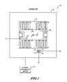
- FIG. 1illustrates a block diagram of a sensor system 38 formed in accordance with an embodiment of the invention.
- the system 38includes a housing 40 defining an enclosed cavity 42 .
- a plurality of stator tines 46extend from the housing 40 into the enclosed cavity 42 .
- a proof mass 48is suspended within the enclosed cavity 42 and includes a plurality of rotor tines 50 that are spaced apart at a capacitive distance from the stator tines 46 .
- the housing 40 , the stator tines 46 , the proof mass 48 , and the rotor tines 50are formed of a double layer silicon on insulator (SOI) material having an insulating layer separating a first section from a second section.
- SOIsilicon on insulator
- the sensor system 38includes a microelectromechanical system (MEMS) accelerometer and/or gyro.
- MEMSmicroelectromechanical system
- the range of the total thicknessis 24 to 100 microns.
- the statoris the full height dimension (24 to 100 microns), and the rotor is roughly 3 ⁇ 4 of that height.
- the stator and rotor tineswould be approximately 3 ⁇ 4 of the total thickness, with a 1 ⁇ 4 offset.
- the thickness of the rotor and stator combswould be 18 microns, with a 6 micron offset.
- a sensor/controller device 51is in signal communication with the sensor system 38 .
- the device 51senses vertical relative motion between the proof mass 48 and the housing 40 . Typically, this sense, or pick-off, would operate capacitively.
- the device 51sends a signal to the stator tines 46 in order to force the rotor tines 50 back to a null position.
- the signale.g., voltage value
- the signalthat is sent to the stator tines 46 for forcing the rotor tines 50 back to null position is used to calculate the amount of acceleration that the proof mass 48 is experiencing.
- the housing 40is shown with a filled isolation trench 52 enclosing a first volume 53 of the first section of the SOI material of the housing 40 that is separated from the remainder of the first section of the SOI material of the housing 40 .
- a conducting structure 54is located within the first volume 53 and extends into the housing 40 , connecting both sections (layers) of the SOI material of which the housing 40 is formed through the insulating layer of the housing 40 .
- the conducting structure 54is connected to ground in an example embodiment, but is connected to a voltage source in other embodiments.
- a contact pad 56is attached to an area of the first section of the SOI material of the housing 40 that is electrically isolated from the first volume 53 by the isolation trench 52 .
- the contact pad 56does not extend through both layers of SOI material of which the housing 40 is formed.
- the contact pad 56is connected to a voltage VB in an example embodiment. This allows the voltage VB to be applied to one layer of the SOI material, while ground or the other applied voltage source is applied to the other layer of the SOI material, resulting in differing voltages on each section (layer) of the stator tines 46 .
- additional structures similar to the isolation trench 52 , the conducting structure 54 , and the contact pad 56are also present in an embodiment.
- a conducting structure 58is located on part of the proof mass 48 in an example embodiment.
- the conducting structure 58extends into the proof mass 48 , connecting both layers of the SOI material of which the proof mass 48 and rotor tines 50 are formed.
- the conducting structure 58is connected to a voltage V A in an example embodiment. This allows the voltage V A to be applied to both layers of the SOI material, so that both layers of the SOI material that form the rotor tines 50 receive the voltage V A .
- the conducting structure 58is shown located on the proof mass 48 in this example, the conducting structure 58 could be located on other structures made of the same SOI material as the rotor tines 50 .
- FIG. 2illustrates a cross-sectional view of components and structures used in an embodiment of the invention.
- An example embodimentis formed in a fabrication process from a starting material 98 .
- the starting material 98includes a silicon handle wafer 100 , a first silicon on insulator (SOI) layer 102 , and a second SOI layer 104 .
- the first SOI layer 102is separated from the handle wafer 100 by a first buried silicon oxide (BOX) layer 106 and from the second SOI layer 104 by a second BOX layer 108 .
- the SOI layers 102 , 104are silicon on oxide layers.
- the fabrication processproduces various structures in the two SOI layers 102 , 104 including a Vertical Comb actuator (VCA) 110 with offset stationary and movable comb fingers.
- VCAVertical Comb actuator
- the processalso produces open trenches and/or structures 112 through both SOI layers 102 , 104 and the second BOX layer 108 ; open structures with the second SOI layer 104 being partially or fully removed; trenches and/or structures in the second SOI layer 104 which are filled with an electrically isolating material 114 ; and structures connecting the first SOI layer 102 and the second SOI layer 104 through the second BOX layer 108 by being filled with an electrically conducting material 116 .
- the forming of structures in the SOI layers 102 , 104 of the silicon wafercan be divided into fabrication steps that include trench filling, device mask patterning, and SOI etching, which are described in additional detail below.
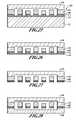
- FIGS. 3-14illustrate cross-sectional views of steps in a trench filling process in accordance with an embodiment of the invention.
- a double SOI wafer 130is used as starting material.
- the wafer 130includes a silicon handle wafer 132 , a first SOI layer 134 , and a second SOI layer 136 .
- the first SOI layer 134is separated from the handle wafer 132 by a first BOX layer 138 and from the second SOI layer 136 by a second BOX layer 140 .
- FIG. 3illustrates a first masking layer 142 being deposited on the wafer 130 surface and patterned with an isolation trench layout 144 , such as by being photo-resist patterned using photo-lithography, for example.
- the patterned first masking layer 142is then used as a mask for etching the second SOI layer 136 in the exposed areas to form a trench 146 , as shown in FIG. 4 .
- the etchingis anisotropic (into the wafer only), which is commonly accomplished by Deep Reactive Ion etching (DRIE) and stops on the second BOX layer 140 .
- DRIEDeep Reactive Ion etching
- the remaining masking layer 142is stripped as shown in FIG. 5 , such as by plasma ashing or in a solvent solution, for example.
- FIGS. 6-8illustrate that the trench 146 is then filled with an electrically isolating and mechanically connecting material.
- the materialcan be a single material or multiple materials, such as silicon dioxide, silicon nitride, poly-silicon, or materials with similar properties. If poly-silicon is used in an example embodiment, sidewalls of the trench 146 are lined with oxide or nitride before the trench center is filled with poly-silicon.
- FIG. 6illustrates one variation, where the trench 146 sidewalls are first lined with an electrically isolating material, shown as a first iso-layer 148 that is formed of thermally grown silicon dioxide in an example embodiment. Then, as shown in FIG. 7 , the center of the trench 146 is filled with another electrically isolating material, shown as a second iso-layer 150 such as Low Pressure Chemical Vapor Deposition (LPCVD) silicon nitride. Next, as illustrated in FIG. 8 , the second iso-layer 150 material is removed from the wafer 130 surface, stopping on the first iso-layer 148 .
- LPCVDLow Pressure Chemical Vapor Deposition
- FIGS. 9-14illustrate additional steps that electrically connect the first and second SOI layers 134 , 136 such as may be used in a portion of a moveable comb electrode.
- FIG. 9shows that a resist mask 152 is patterned on the wafer surface with a contact trench/hole layout 154 . In an example embodiment, this is formed using photolithography with the pattern being transferred into the first iso-layer 148 below, such as by reactive ion etching (RIE), for example.
- RIEreactive ion etching
- a silicon etching stepfollows where the second SOI layer 136 is etched in an exposed area 156 to the second BOX layer 140 . In an example embodiment, etching is anisotropic (into the wafer only), such as by DRIE.
- the second BOX layer 140is removed in an unmasked area to form an open contact trench 158 such as by RIE or in a diluted hydrogen fluoride (HF) solution.
- the remaining resist mask 152 on the wafer surfaceis stripped such as by plasma ashing or in a solvent solution, for example.
- the open contact trench 158is filled with an electrically conductive material 160 , such as insitu doped poly-silicon deposited by LPCVD, electrically connecting the second SOI layer 136 and the first SOI layer 134 .
- the conductive layer and the first isolayer 148are removed from the wafer surface.
- thisis done by silicon RIE and oxide RIE, or by wafer surface grinding and polishing.
- the resulting waferis a double SOI material with an embedded isolation trench 162 and a contact trench 164 .
- the wafermay include various numbers and structures of isolation and contact trenches 162 , 164 .
- FIGS. 15-18illustrate cross-sectional views of steps in a device mask patterning process in accordance with an embodiment of the invention.
- the starting material shown in FIG. 15is a double SOI wafer 170 .
- the wafer 170includes a silicon handle wafer 172 , a first SOI layer 174 , and a second SOI layer 176 .
- the first SOI layer 174is separated from the handle wafer 172 by a first BOX layer 178 and from the second SOI layer 176 by a second BOX layer 180 .
- a first mask 182such as an oxide mask is deposited and patterned with a plurality of stationary elements 184 , such as stator components of a VCA, and with patterns defining the mechanical structure of the sensor (not shown).
- a second mask 186such as a resist mask, is deposited and patterned with stationary 188 and movable elements 190 of the VCA as well as with sensor patterns requiring etching through both SOI layers 174 , 176 and the second BOX layer 180 , such as a proof mass, beams, flexures, proof mass anchors, and proof mass perforations (all not shown).
- the stationary comb elements 188 defined in the second mask 186are smaller than the stationary comb elements 184 defined in the first mask 182 .
- the pattern of the second mask 186is transferred into the underlying first mask 182 to form a modified first mask 192 as shown in FIG. 18 , such as by RIE.
- the resulting multi-layer maskincludes the second mask material (resist) for the movable elements of the VCA, and the modified first mask 192 and second mask 186 material for the stationary elements of the VCA and for the other sensor structure patterns (not shown).
- the masking methodcan be repeated to deposit and pattern additional masks, defining multiple etch depths into the second SOI layer 176 or to completely remove the second layer 176 in open areas.
- stator and rotor elementsby the same mask (second mask 186 ) self-aligns the stator to rotor pattern by centering a rotor element 194 between two stator elements 196 .
- FIGS. 19-24illustrate cross-sectional views of steps in a Silicon-On-Insulator (SOI) etching process in accordance with an embodiment of the invention.
- SOISilicon-On-Insulator
- the second SOI layer 176is etched to the second BOX layer 180 using the multi-layer mask including masks 186 , 192 as an etch mask to form the structure shown in FIG. 19 .
- Etchingis anisotropic, into the wafer only, which is commonly accomplished by DRIE using sulfur hexafluoride (SF 6 ) and octafluorocyclobutane (C 4 F 8 ) as precursors.
- the second BOX layer 180is removed in exposed areas 198 , such as by RIE or in a diluted HF solution to form the structure shown in FIG. 20 .
- the first SOI layer 174is etched to the first BOX layer 178 in exposed areas 200 to form the structure shown in FIG. 21 .
- Etchingis anisotropic as during the first silicon etching step.
- the remaining second mask 186 (resist) of the double-layer surface maskis selectively removed, such as by plasma ashing using an oxygen precursor or in a solvent solution to form the structure shown in FIG. 22 .
- Thisexposes the movable comb elements 194 of the VCA as well as other device structures requiring a thinned second SOI layer 176 , while the stationary comb elements 196 of the VCA are still masked by the modified first mask layer 192 (oxide).
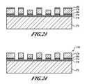
- the second SOI layer 176is etched in the exposed areas of the movable comb elements 194 of the VCA to form the structure shown in FIG. 23 .
- the etching directionis into the wafer again, as during the previous silicon etching steps, preserving the previously etched structures.
- the etchingis timed such that the movable comb elements 194 as well as other device structures (not shown) requiring a thinned second SOI layer 176 are shortened to a pre-defined height.
- the method of etching the second SOI layer 176would be modified such that the deepest structure is opened first (by removing its mask) and then etched to a depth of its final etch depth minus the etch depths of the following second SOI layer 176 etches. The process is repeated for other structures with different etch depths in the second SOI layer 176 , with the most shallow etch being executed last.
- the remaining modified first mask layer 192(oxide) is removed from the surface of the processed wafer 170 to form the structure shown in FIG. 24 , such as by RIE or etching in a diluted HF solution.
- RIEreactive ion etching
- anisotropic reactive ion etchingis the preferred method, taking advantage of its higher surface etch rate compared to the first BOX layer 178 etch rate, and a nearly zero etch rate of the second BOX layer 180 .
- FIGS. 25-28illustrate cross sectional views of steps performed after SOI etching in accordance with an embodiment of the invention.
- the processed SOI wafer 170is bonded to a first cover 210 to form the structure shown in FIG. 25 .
- the cover 210is formed of a glass substrate, such as pyrex, in which various structures (not shown) have been separately fabricated in an example embodiment of the invention.
- anodic bonding or bonding using an inter-layer adhesivesuch as glass-frit, polymer, or metal can be used for attaching the cover 210 to the processed SOI wafer 170 .
- Sets of electrodes of the parallel plate typeare formed between the processed SOI wafer 170 and the cover 210 by using silicon structures (not shown) as a movable electrode and metal pads (not shown) on the cover 210 as a stationary electrode.
- the electrodesare separated by a gap which is formed by etching a recess into the cover 210 .
- the cover 210also provides metallized contact pads (not shown) connected to the second SOI layer 176 , metallized contact pads (not shown) in recessed areas for wire-bonding to a sensor package, and metal lines (not shown) between the contact pads.
- the silicon handle wafer 172is removed, stopping on the first BOX layer 178 to form the structure shown in FIG. 26 .
- thiscan be done by a combination of processes or by a single process that include grinding, polishing, and etching processes selective to oxide, including wet chemical etching in alkaline solutions such as potassium hydroxide (KOH), ethylene diamine-pyrocatechol (EDP), and tetramethyl ammonium hydroxide (TMAH) as well as plasma etching using fluorine radicals.
- KOHpotassium hydroxide
- EDPethylene diamine-pyrocatechol
- TMAHtetramethyl ammonium hydroxide
- the exposed oxide layer of the first BOX layer 178is removed stopping on the first SOI layer 174 to form the structure shown in FIG. 27 .
- thiscan be done by an etching process selective to silicon, such as by plasma etching using carbon tetrafluoride (CF 4 )/carbon hydro-trifluoride (CHF 3 ) precursors or by wet chemical etching in a diluted hydrogen fluoride (HF) solution.
- etching processselective to silicon, such as by plasma etching using carbon tetrafluoride (CF 4 )/carbon hydro-trifluoride (CHF 3 ) precursors or by wet chemical etching in a diluted hydrogen fluoride (HF) solution.
- CF 4carbon tetrafluoride
- CHF 3carbon hydro-trifluoride
- HFdiluted hydrogen fluoride
- a second cover 220is bonded to the first SOI layer 174 to form the structure shown in FIG. 28 .
- the second cover 220is formed of a glass substrate, such as pyrex, in an example embodiment of the invention.
- Anodic bonding, or bonding using an interlayer adhesivesuch as glass frit, polymer, or metal can be used for attaching the second cover 220 to the first SOI layer 174 .
- the second cover 220includes structures (not shown) previously formed in it, including recesses, metal electrode pads, metal pads used to connect to the first SOI layer 174 , metal lines connecting the pads, and/or open access areas for wire bonding to the second cover 220 .
- Devicesare then singulated from the wafer assembly such as by dicing, for example. This may require protecting the devices from process residues during singulation and/or cleaning of the devices.
Landscapes
- Physics & Mathematics (AREA)
- General Physics & Mathematics (AREA)
- Engineering & Computer Science (AREA)
- Radar, Positioning & Navigation (AREA)
- Remote Sensing (AREA)
- Micromachines (AREA)
- Pressure Sensors (AREA)
- Gyroscopes (AREA)
Abstract
Description
- High performance Micro-Electro-Mechanical Systems (MEMS) inertial instruments (accelerometers and gyros) require closed-loop operation. Good performance under vibration requires that the magnitude of the electrostatic feedback force be highly insensitive to the position of the instrument's inertial mass relative to it's null position. Because of their high force dependency on position, the typical electrostatic vertical comb drive as employed in MEMS actuators cannot be applied to precision MEMS inertial instruments. There have been attempts to provide an electrostatic MEMS drive with very low position sensitivity, but they have been costly due to the numerous manufacturing steps required.
- Therefore, there exists a need for an electrostatic MEMS drive, which has very low position sensitivity.
- An example embodiment of the present invention includes a micoroelectromechanical system (MEMS) that includes a housing formed from a double layer silicon on insulator (SOI) material having an insulating layer separating a first section from a second section, the housing defining an enclosed cavity such that the insulating layer from the housing SOI material runs along a length of each stator tine and is disposed between a first section of each stator tine extending a first distance from the insulating layer and a second section of each stator tine extending a second distance from the insulating layer in an opposite direction from the first section, the first section of each stator tine being electrically connected to the first section of the housing and the second section of each stator tine being electrically connected to the second section of the housing; one or more stator tines extending from the housing into the cavity; a MEMS device located within the cavity, the MEMS device including a proof mass formed from a double layer SOI material having an insulating layer separating a first section from a second section, the proof mass coupled to the housing; and one or more rotor tines extending from the proof mass such that the insulating layer from the proof mass SOI material runs along a length of each rotor tine and is disposed between a first section of each rotor tine extending a first distance from the insulating layer and a second section of each rotor tine extending a second distance from the insulating layer in an opposite direction from the first section, each rotor tine being positioned at a capacitive distance from a corresponding stator tine, the first section of each rotor tine being electrically connected to the first section of the proof mass and the second section of each rotor tine being electrically connected to the second section of the proof mass. In an example embodiment, the proof mass is configured to deflect in a direction approximately orthogonal to a vector normal between the corresponding tines and the stator tine first distance is greater than the rotor tine first distance.
- In accordance with further aspects of the invention, the stator tine second distance is approximately equal to the rotor tine second distance.
- In accordance with other aspects of the invention, the system includes a contact structure that electrically connects the first section of the rotor tines to the second section of the rotor tines through at least one of the insulating layer of the proof mass or the insulating layer of the rotor tines.
- In accordance with still further aspects of the invention, the insulating layer of the rotor tines and the insulating layer of the stator tines are oxide layers.
- In accordance with yet other aspects of the invention, the system includes a contact structure that electrically connects a first portion of the first section of the housing to a first portion of the second section of the housing through a region of the insulating layer of the housing. The example system also includes an isolation trench that electrically isolates the first portion of the first section of the housing from a second portion of the first section of the housing, the first section of the stator tines remaining electrically connected to the second portion of the first section of the housing and the second section of the stator tines remaining electrically connected to the second portion of the second section of the housing while the second portion of the first section of the housing remains electrically isolated from the second portion of the second section of the housing.
- In accordance with still further aspects of the invention, the MEMS device includes a sensor such as an accelerometer or a gyro.
- As will be readily appreciated from the foregoing summary, the invention provides a microelectromechanical system including a MEMS device using position-independent drive electrodes in a multi-layer substrate.
- Preferred and alternative embodiments of the present invention are described in detail below with reference to the following drawings:
FIG. 1 illustrates a block diagram of a sensor system formed in accordance with an embodiment of the invention;FIG. 2 illustrates a cross-sectional view of components used in an embodiment of the invention;FIGS. 3-14 illustrate cross-sectional views of steps in a trench filling process in accordance with an embodiment of the invention;FIGS. 15-18 illustrate cross-sectional views of steps in a device mask patterning process in accordance with an embodiment of the invention;FIGS. 19-24 illustrate cross-sectional views of steps in a Silicon-On-Insulator (SOI) etching process in accordance with an embodiment of the invention; andFIGS. 25-28 illustrate cross sectional views of steps performed after SOI etching in accordance with an embodiment of the invention.FIG. 1 illustrates a block diagram of asensor system 38 formed in accordance with an embodiment of the invention. Thesystem 38 includes ahousing 40 defining an enclosedcavity 42. A plurality ofstator tines 46 extend from thehousing 40 into the enclosedcavity 42. Aproof mass 48 is suspended within the enclosedcavity 42 and includes a plurality ofrotor tines 50 that are spaced apart at a capacitive distance from thestator tines 46. In an example embodiment, thehousing 40, the stator tines46, theproof mass 48, and therotor tines 50 are formed of a double layer silicon on insulator (SOI) material having an insulating layer separating a first section from a second section. In an example embodiment, thesensor system 38 includes a microelectromechanical system (MEMS) accelerometer and/or gyro.- The range of the total thickness is 24 to 100 microns. The stator is the full height dimension (24 to 100 microns), and the rotor is roughly ¾ of that height. The stator and rotor tines would be approximately ¾ of the total thickness, with a ¼ offset. For Example, if the total thickness is 24 microns, then the thickness of the rotor and stator combs would be 18 microns, with a 6 micron offset.
- A sensor/
controller device 51 is in signal communication with thesensor system 38. In an example embodiment, thedevice 51 senses vertical relative motion between theproof mass 48 and thehousing 40. Typically, this sense, or pick-off, would operate capacitively. In closed-loop operation, once thedevice 51 senses a proof mass movement, thedevice 51 sends a signal to thestator tines 46 in order to force therotor tines 50 back to a null position. The signal (e.g., voltage value) that is sent to thestator tines 46 for forcing the rotor tines50 back to null position is used to calculate the amount of acceleration that theproof mass 48 is experiencing. - The
housing 40 is shown with a filledisolation trench 52 enclosing afirst volume 53 of the first section of the SOI material of thehousing 40 that is separated from the remainder of the first section of the SOI material of thehousing 40. Aconducting structure 54 is located within thefirst volume 53 and extends into thehousing 40, connecting both sections (layers) of the SOI material of which thehousing 40 is formed through the insulating layer of thehousing 40. Theconducting structure 54 is connected to ground in an example embodiment, but is connected to a voltage source in other embodiments. A contact pad56 is attached to an area of the first section of the SOI material of thehousing 40 that is electrically isolated from thefirst volume 53 by theisolation trench 52. In an example embodiment, the contact pad56 does not extend through both layers of SOI material of which thehousing 40 is formed. The contact pad56 is connected to a voltage VB in an example embodiment. This allows the voltage VB to be applied to one layer of the SOI material, while ground or the other applied voltage source is applied to the other layer of the SOI material, resulting in differing voltages on each section (layer) of thestator tines 46. Although not shown, additional structures similar to theisolation trench 52, the conductingstructure 54, and the contact pad56 are also present in an embodiment. - A conducting
structure 58 is located on part of theproof mass 48 in an example embodiment. Theconducting structure 58 extends into theproof mass 48, connecting both layers of the SOI material of which theproof mass 48 androtor tines 50 are formed. Theconducting structure 58 is connected to a voltage VAin an example embodiment. This allows the voltage VAto be applied to both layers of the SOI material, so that both layers of the SOI material that form therotor tines 50 receive the voltage VA. Although the conductingstructure 58 is shown located on theproof mass 48 in this example, the conductingstructure 58 could be located on other structures made of the same SOI material as therotor tines 50. FIG. 2 illustrates a cross-sectional view of components and structures used in an embodiment of the invention. An example embodiment is formed in a fabrication process from astarting material 98. Thestarting material 98 includes asilicon handle wafer 100, a first silicon on insulator (SOI)layer 102, and asecond SOI layer 104. Thefirst SOI layer 102 is separated from thehandle wafer 100 by a first buried silicon oxide (BOX)layer 106 and from thesecond SOI layer 104 by asecond BOX layer 108. In an example embodiment, theSOI layers - The fabrication process produces various structures in the two
SOI layers structures 112 through bothSOI layers second BOX layer 108; open structures with thesecond SOI layer 104 being partially or fully removed; trenches and/or structures in thesecond SOI layer 104 which are filled with an electrically isolatingmaterial 114; and structures connecting thefirst SOI layer 102 and thesecond SOI layer 104 through thesecond BOX layer 108 by being filled with an electrically conductingmaterial 116. - In an example embodiment, the forming of structures in the
SOI layers FIGS. 3-14 illustrate cross-sectional views of steps in a trench filling process in accordance with an embodiment of the invention. Adouble SOI wafer 130 is used as starting material. In similar fashion to that described forFIG. 2 , thewafer 130 includes asilicon handle wafer 132, afirst SOI layer 134, and asecond SOI layer 136. Thefirst SOI layer 134 is separated from thehandle wafer 132 by afirst BOX layer 138 and from thesecond SOI layer 136 by asecond BOX layer 140.FIG. 3 illustrates afirst masking layer 142 being deposited on thewafer 130 surface and patterned with anisolation trench layout 144, such as by being photo-resist patterned using photo-lithography, for example. The patternedfirst masking layer 142 is then used as a mask for etching thesecond SOI layer 136 in the exposed areas to form atrench 146, as shown inFIG. 4 . In an example embodiment, the etching is anisotropic (into the wafer only), which is commonly accomplished by Deep Reactive Ion etching (DRIE) and stops on thesecond BOX layer 140. After silicon etching, the remainingmasking layer 142 is stripped as shown inFIG. 5 , such as by plasma ashing or in a solvent solution, for example.FIGS. 6-8 illustrate that thetrench 146 is then filled with an electrically isolating and mechanically connecting material. The material can be a single material or multiple materials, such as silicon dioxide, silicon nitride, poly-silicon, or materials with similar properties. If poly-silicon is used in an example embodiment, sidewalls of thetrench 146 are lined with oxide or nitride before the trench center is filled with poly-silicon.FIG. 6 illustrates one variation, where thetrench 146 sidewalls are first lined with an electrically isolating material, shown as a first iso-layer 148 that is formed of thermally grown silicon dioxide in an example embodiment. Then, as shown inFIG. 7 , the center of thetrench 146 is filled with another electrically isolating material, shown as a second iso-layer 150 such as Low Pressure Chemical Vapor Deposition (LPCVD) silicon nitride. Next, as illustrated inFIG. 8 , the second iso-layer 150 material is removed from thewafer 130 surface, stopping on the first iso-layer 148.FIGS. 9-14 illustrate additional steps that electrically connect the first and second SOI layers134,136 such as may be used in a portion of a moveable comb electrode.FIG. 9 shows that a resistmask 152 is patterned on the wafer surface with a contact trench/hole layout 154. In an example embodiment, this is formed using photolithography with the pattern being transferred into the first iso-layer 148 below, such as by reactive ion etching (RIE), for example. Next, as shown inFIG. 10 , a silicon etching step follows where thesecond SOI layer 136 is etched in an exposedarea 156 to thesecond BOX layer 140. In an example embodiment, etching is anisotropic (into the wafer only), such as by DRIE. Next, as shown inFIG. 11 , thesecond BOX layer 140 is removed in an unmasked area to form anopen contact trench 158 such as by RIE or in a diluted hydrogen fluoride (HF) solution. Then, as shown inFIG. 12 , the remaining resistmask 152 on the wafer surface is stripped such as by plasma ashing or in a solvent solution, for example. As shown inFIG. 13 , theopen contact trench 158 is filled with an electricallyconductive material 160, such as insitu doped poly-silicon deposited by LPCVD, electrically connecting thesecond SOI layer 136 and thefirst SOI layer 134. Next, as shown inFIG. 14 , the conductive layer and thefirst isolayer 148 are removed from the wafer surface. In some embodiments, this is done by silicon RIE and oxide RIE, or by wafer surface grinding and polishing. The resulting wafer is a double SOI material with an embeddedisolation trench 162 and acontact trench 164. The wafer may include various numbers and structures of isolation andcontact trenches FIGS. 15-18 illustrate cross-sectional views of steps in a device mask patterning process in accordance with an embodiment of the invention. The starting material shown inFIG. 15 is adouble SOI wafer 170. In similar fashion to that described forFIG. 3 , thewafer 170 includes asilicon handle wafer 172, afirst SOI layer 174, and asecond SOI layer 176. Thefirst SOI layer 174 is separated from thehandle wafer 172 by afirst BOX layer 178 and from thesecond SOI layer 176 by asecond BOX layer 180.- A
first mask 182, such as an oxide mask is deposited and patterned with a plurality ofstationary elements 184, such as stator components of a VCA, and with patterns defining the mechanical structure of the sensor (not shown). Asecond mask 186, such as a resist mask, is deposited and patterned with stationary188 andmovable elements 190 of the VCA as well as with sensor patterns requiring etching through both SOI layers174,176 and thesecond BOX layer 180, such as a proof mass, beams, flexures, proof mass anchors, and proof mass perforations (all not shown). Thestationary comb elements 188 defined in thesecond mask 186 are smaller than thestationary comb elements 184 defined in thefirst mask 182. - After patterning of the
second mask 186, the pattern of thesecond mask 186 is transferred into the underlyingfirst mask 182 to form a modifiedfirst mask 192 as shown inFIG. 18 , such as by RIE. The resulting multi-layer mask includes the second mask material (resist) for the movable elements of the VCA, and the modifiedfirst mask 192 andsecond mask 186 material for the stationary elements of the VCA and for the other sensor structure patterns (not shown). The masking method can be repeated to deposit and pattern additional masks, defining multiple etch depths into thesecond SOI layer 176 or to completely remove thesecond layer 176 in open areas. - The definition of the stator and rotor elements by the same mask (second mask186) self-aligns the stator to rotor pattern by centering a rotor element194 between two
stator elements 196. FIGS. 19-24 illustrate cross-sectional views of steps in a Silicon-On-Insulator (SOI) etching process in accordance with an embodiment of the invention. During a first silicon etching step, thesecond SOI layer 176 is etched to thesecond BOX layer 180 using the multi-layermask including masks FIG. 19 . Etching is anisotropic, into the wafer only, which is commonly accomplished by DRIE using sulfur hexafluoride (SF6) and octafluorocyclobutane (C4F8) as precursors. Next, thesecond BOX layer 180 is removed in exposedareas 198, such as by RIE or in a diluted HF solution to form the structure shown inFIG. 20 .- During a second silicon etching step, the
first SOI layer 174 is etched to thefirst BOX layer 178 in exposedareas 200 to form the structure shown inFIG. 21 . Etching is anisotropic as during the first silicon etching step. Next, the remaining second mask186 (resist) of the double-layer surface mask is selectively removed, such as by plasma ashing using an oxygen precursor or in a solvent solution to form the structure shown inFIG. 22 . This exposes the movable comb elements194 of the VCA as well as other device structures requiring a thinnedsecond SOI layer 176, while thestationary comb elements 196 of the VCA are still masked by the modified first mask layer192 (oxide). During a third silicon etching step, thesecond SOI layer 176 is etched in the exposed areas of the movable comb elements194 of the VCA to form the structure shown inFIG. 23 . The etching direction is into the wafer again, as during the previous silicon etching steps, preserving the previously etched structures. The etching is timed such that the movable comb elements194 as well as other device structures (not shown) requiring a thinnedsecond SOI layer 176 are shortened to a pre-defined height. - If additional masking layers (not shown) were deposited and patterned, the method of etching the
second SOI layer 176 would be modified such that the deepest structure is opened first (by removing its mask) and then etched to a depth of its final etch depth minus the etch depths of the followingsecond SOI layer 176 etches. The process is repeated for other structures with different etch depths in thesecond SOI layer 176, with the most shallow etch being executed last. - Then, the remaining modified first mask layer192 (oxide) is removed from the surface of the processed
wafer 170 to form the structure shown inFIG. 24 , such as by RIE or etching in a diluted HF solution. During this mask-stripping step, care must be taken to not completely remove thefirst BOX layer 178 which would release the SOI structures prematurely. Therefore, anisotropic reactive ion etching is the preferred method, taking advantage of its higher surface etch rate compared to thefirst BOX layer 178 etch rate, and a nearly zero etch rate of thesecond BOX layer 180. FIGS. 25-28 illustrate cross sectional views of steps performed after SOI etching in accordance with an embodiment of the invention. After mechanical structures are fabricated in the SOI layers174,176, the processedSOI wafer 170 is bonded to afirst cover 210 to form the structure shown inFIG. 25 . Thecover 210 is formed of a glass substrate, such as pyrex, in which various structures (not shown) have been separately fabricated in an example embodiment of the invention. As examples, anodic bonding or bonding using an inter-layer adhesive such as glass-frit, polymer, or metal can be used for attaching thecover 210 to the processedSOI wafer 170. Sets of electrodes of the parallel plate type are formed between the processedSOI wafer 170 and thecover 210 by using silicon structures (not shown) as a movable electrode and metal pads (not shown) on thecover 210 as a stationary electrode. The electrodes are separated by a gap which is formed by etching a recess into thecover 210. In an example embodiment, thecover 210 also provides metallized contact pads (not shown) connected to thesecond SOI layer 176, metallized contact pads (not shown) in recessed areas for wire-bonding to a sensor package, and metal lines (not shown) between the contact pads.- After the processed
SOI wafer 170 with the SOI layers174,176 has been bonded to thefirst cover 210, thesilicon handle wafer 172 is removed, stopping on thefirst BOX layer 178 to form the structure shown inFIG. 26 . As examples, this can be done by a combination of processes or by a single process that include grinding, polishing, and etching processes selective to oxide, including wet chemical etching in alkaline solutions such as potassium hydroxide (KOH), ethylene diamine-pyrocatechol (EDP), and tetramethyl ammonium hydroxide (TMAH) as well as plasma etching using fluorine radicals. - Next, the exposed oxide layer of the
first BOX layer 178, is removed stopping on thefirst SOI layer 174 to form the structure shown inFIG. 27 . As examples, this can be done by an etching process selective to silicon, such as by plasma etching using carbon tetrafluoride (CF4)/carbon hydro-trifluoride (CHF3) precursors or by wet chemical etching in a diluted hydrogen fluoride (HF) solution. This process releases movable silicon structures previously formed in the SOI layers. - In some embodiments, a
second cover 220 is bonded to thefirst SOI layer 174 to form the structure shown inFIG. 28 . Thesecond cover 220 is formed of a glass substrate, such as pyrex, in an example embodiment of the invention. Anodic bonding, or bonding using an interlayer adhesive such as glass frit, polymer, or metal can be used for attaching thesecond cover 220 to thefirst SOI layer 174. In some embodiments, thesecond cover 220 includes structures (not shown) previously formed in it, including recesses, metal electrode pads, metal pads used to connect to thefirst SOI layer 174, metal lines connecting the pads, and/or open access areas for wire bonding to thesecond cover 220. - Devices are then singulated from the wafer assembly such as by dicing, for example. This may require protecting the devices from process residues during singulation and/or cleaning of the devices.
- While the preferred embodiment of the invention has been illustrated and described, as noted above, many changes can be made without departing from the spirit and scope of the invention. Accordingly, the scope of the invention is not limited by the disclosure of the preferred embodiment. Instead, the invention should be determined entirely by reference to the claims that follow.
Claims (12)
Priority Applications (3)
| Application Number | Priority Date | Filing Date | Title |
|---|---|---|---|
| US11/829,014US7690254B2 (en) | 2007-07-26 | 2007-07-26 | Sensor with position-independent drive electrodes in multi-layer silicon on insulator substrate |
| EP08161132.9AEP2023151B1 (en) | 2007-07-26 | 2008-07-24 | Sensor with position-indepedent drive electrodes in multi-layer silicon on insulator substrate |
| JP2008193358AJP2009150863A (en) | 2007-07-26 | 2008-07-28 | Sensor with position-independent driver electrodes in a multilayer silicon-on-insulator substrate |
Applications Claiming Priority (1)
| Application Number | Priority Date | Filing Date | Title |
|---|---|---|---|
| US11/829,014US7690254B2 (en) | 2007-07-26 | 2007-07-26 | Sensor with position-independent drive electrodes in multi-layer silicon on insulator substrate |
Publications (2)
| Publication Number | Publication Date |
|---|---|
| US20090025477A1true US20090025477A1 (en) | 2009-01-29 |
| US7690254B2 US7690254B2 (en) | 2010-04-06 |
Family
ID=39941875
Family Applications (1)
| Application Number | Title | Priority Date | Filing Date |
|---|---|---|---|
| US11/829,014Active2027-08-27US7690254B2 (en) | 2007-07-26 | 2007-07-26 | Sensor with position-independent drive electrodes in multi-layer silicon on insulator substrate |
Country Status (3)
| Country | Link |
|---|---|
| US (1) | US7690254B2 (en) |
| EP (1) | EP2023151B1 (en) |
| JP (1) | JP2009150863A (en) |
Cited By (9)
| Publication number | Priority date | Publication date | Assignee | Title |
|---|---|---|---|---|
| US20110005317A1 (en)* | 2009-07-09 | 2011-01-13 | Honeywell International Inc. | Translational mass in-plane mems accelerometer |
| US20110092018A1 (en)* | 2007-09-28 | 2011-04-21 | Honeywell International Inc. | Wafer level packaged mems device |
| US20110203372A1 (en)* | 2010-02-19 | 2011-08-25 | Honeywell International Inc. | Out-of-plane comb-drive accelerometer |
| US20130057757A1 (en)* | 2010-05-20 | 2013-03-07 | Lg Innotek Co., Ltd. | Camera module having mems actuator, connecting method for shutter coil of camera module and camera module manufactured by the same method |
| WO2017059056A1 (en)* | 2015-09-30 | 2017-04-06 | Mems Drive, Inc. | Mems grid for manipulating structural parameters of mems devices |
| US9630836B2 (en) | 2015-09-30 | 2017-04-25 | Mems Drive, Inc. | Simplified MEMS device fabrication process |
| CN107271719A (en)* | 2016-03-31 | 2017-10-20 | 意法半导体股份有限公司 | With high accuracy and to temperature and the MEMS acceleration measurements sensors of aging hyposensitivity |
| EP3409639A1 (en)* | 2017-05-30 | 2018-12-05 | Murata Manufacturing Co., Ltd. | Method for recess etching in micromechanical devices |
| US20220293558A1 (en)* | 2016-09-02 | 2022-09-15 | Infineon Technologies Ag | Method for forming semiconductor devices using a glass structure attached to a wide band-gap semiconductor wafer |
Families Citing this family (17)
| Publication number | Priority date | Publication date | Assignee | Title |
|---|---|---|---|---|
| JP2009216693A (en)* | 2008-02-13 | 2009-09-24 | Denso Corp | Physical sensor |
| JP2010286471A (en)* | 2009-05-15 | 2010-12-24 | Seiko Epson Corp | MEMS sensors, electronic devices |
| US8418555B2 (en)* | 2009-06-26 | 2013-04-16 | Honeywell International Inc. | Bidirectional, out-of-plane, comb drive accelerometer |
| US9493344B2 (en) | 2010-11-23 | 2016-11-15 | Honeywell International Inc. | MEMS vertical comb structure with linear drive/pickoff |
| US8748206B2 (en) | 2010-11-23 | 2014-06-10 | Honeywell International Inc. | Systems and methods for a four-layer chip-scale MEMS device |
| US8776601B2 (en) | 2010-11-23 | 2014-07-15 | Honeywell International Inc. | MEMS sensor using multi-layer movable combs |
| US9171964B2 (en) | 2010-11-23 | 2015-10-27 | Honeywell International Inc. | Systems and methods for a three-layer chip-scale MEMS device |
| ITTO20120179A1 (en)* | 2012-02-28 | 2013-08-29 | St Microelectronics Srl | MICROELETTROMECHANICAL SENSOR WITH OUT OF PLAN DETECTION AND PROCEDURE FOR THE MANUFACTURE OF A MICROELETTROMECANICAL SENSOR |
| WO2015013828A1 (en) | 2013-08-02 | 2015-02-05 | Motion Engine Inc. | Mems motion sensor and method of manufacturing |
| JP6467347B2 (en)* | 2013-11-07 | 2019-02-13 | 住友精密工業株式会社 | Semiconductor device |
| US20170030788A1 (en) | 2014-04-10 | 2017-02-02 | Motion Engine Inc. | Mems pressure sensor |
| WO2015184531A1 (en) | 2014-06-02 | 2015-12-10 | Motion Engine Inc. | Multi-mass mems motion sensor |
| US11287486B2 (en) | 2014-12-09 | 2022-03-29 | Motion Engine, Inc. | 3D MEMS magnetometer and associated methods |
| FI127229B (en) | 2015-03-09 | 2018-02-15 | Murata Manufacturing Co | Microelectromechanical structure and device |
| US10352960B1 (en)* | 2015-10-30 | 2019-07-16 | Garmin International, Inc. | Free mass MEMS accelerometer |
| EP3650909B1 (en) | 2017-07-06 | 2023-11-15 | Hamamatsu Photonics K.K. | Optical module |
| EP4428542B1 (en)* | 2023-03-07 | 2025-06-18 | Murata Manufacturing Co., Ltd. | In-plane and out-of-plane accelerometer |
Citations (8)
| Publication number | Priority date | Publication date | Assignee | Title |
|---|---|---|---|---|
| US5696848A (en)* | 1995-03-09 | 1997-12-09 | Eastman Kodak Company | System for creating a high resolution image from a sequence of lower resolution motion images |
| US6000280A (en)* | 1995-07-20 | 1999-12-14 | Cornell Research Foundation, Inc. | Drive electrodes for microfabricated torsional cantilevers |
| US6277666B1 (en)* | 1999-06-24 | 2001-08-21 | Honeywell Inc. | Precisely defined microelectromechanical structures and associated fabrication methods |
| US20020005976A1 (en)* | 2000-03-24 | 2002-01-17 | Behrang Behin | Multi-layer, self-aligned vertical combdrive electrostatic actuators and fabrication methods |
| US6582985B2 (en)* | 2000-12-27 | 2003-06-24 | Honeywell International Inc. | SOI/glass process for forming thin silicon micromachined structures |
| US6705116B2 (en)* | 2001-04-10 | 2004-03-16 | Asahi Glass Company, Limited | Method and an apparatus for bending a glass sheet |
| US7270003B2 (en)* | 2004-07-29 | 2007-09-18 | Stmicroelectronics S.R.L. | BMEMS-type high-sensitivity inertial sensor and manufacturing process thereof |
| US7469588B2 (en)* | 2006-05-16 | 2008-12-30 | Honeywell International Inc. | MEMS vertical comb drive with improved vibration performance |
Family Cites Families (8)
| Publication number | Priority date | Publication date | Assignee | Title |
|---|---|---|---|---|
| JPH08166405A (en) | 1994-12-15 | 1996-06-25 | Murata Mfg Co Ltd | Acceleration sensor |
| KR100293806B1 (en) | 1997-06-25 | 2001-10-24 | 박종섭 | LCD |
| FR2810976B1 (en)* | 2000-06-29 | 2003-08-29 | Planhead Silmag P H S | ELECTRONIC MICRO-COMPONENT, SENSOR AND ACTUATOR INCORPORATING SUCH A MICRO-COMPONENT |
| JP2002076311A (en)* | 2000-09-01 | 2002-03-15 | Seiko Epson Corp | Semiconductor device and method of manufacturing the same |
| JP2004354108A (en)* | 2003-05-27 | 2004-12-16 | Matsushita Electric Works Ltd | Angular velocity sensor and its manufacturing method |
| US6936491B2 (en)* | 2003-06-04 | 2005-08-30 | Robert Bosch Gmbh | Method of fabricating microelectromechanical systems and devices having trench isolated contacts |
| JP2006041960A (en) | 2004-07-28 | 2006-02-09 | Nec Corp | Turbo decoding device and turbo decoding method and program |
| US7258010B2 (en)* | 2005-03-09 | 2007-08-21 | Honeywell International Inc. | MEMS device with thinned comb fingers |
- 2007
- 2007-07-26USUS11/829,014patent/US7690254B2/enactiveActive
- 2008
- 2008-07-24EPEP08161132.9Apatent/EP2023151B1/ennot_activeCeased
- 2008-07-28JPJP2008193358Apatent/JP2009150863A/enactivePending
Patent Citations (10)
| Publication number | Priority date | Publication date | Assignee | Title |
|---|---|---|---|---|
| US5696848A (en)* | 1995-03-09 | 1997-12-09 | Eastman Kodak Company | System for creating a high resolution image from a sequence of lower resolution motion images |
| US6000280A (en)* | 1995-07-20 | 1999-12-14 | Cornell Research Foundation, Inc. | Drive electrodes for microfabricated torsional cantilevers |
| US6277666B1 (en)* | 1999-06-24 | 2001-08-21 | Honeywell Inc. | Precisely defined microelectromechanical structures and associated fabrication methods |
| US20020005976A1 (en)* | 2000-03-24 | 2002-01-17 | Behrang Behin | Multi-layer, self-aligned vertical combdrive electrostatic actuators and fabrication methods |
| US6612029B2 (en)* | 2000-03-24 | 2003-09-02 | Onix Microsystems | Multi-layer, self-aligned vertical combdrive electrostatic actuators and fabrication methods |
| US6744173B2 (en)* | 2000-03-24 | 2004-06-01 | Analog Devices, Inc. | Multi-layer, self-aligned vertical combdrive electrostatic actuators and fabrication methods |
| US6582985B2 (en)* | 2000-12-27 | 2003-06-24 | Honeywell International Inc. | SOI/glass process for forming thin silicon micromachined structures |
| US6705116B2 (en)* | 2001-04-10 | 2004-03-16 | Asahi Glass Company, Limited | Method and an apparatus for bending a glass sheet |
| US7270003B2 (en)* | 2004-07-29 | 2007-09-18 | Stmicroelectronics S.R.L. | BMEMS-type high-sensitivity inertial sensor and manufacturing process thereof |
| US7469588B2 (en)* | 2006-05-16 | 2008-12-30 | Honeywell International Inc. | MEMS vertical comb drive with improved vibration performance |
Cited By (23)
| Publication number | Priority date | Publication date | Assignee | Title |
|---|---|---|---|---|
| US20110092018A1 (en)* | 2007-09-28 | 2011-04-21 | Honeywell International Inc. | Wafer level packaged mems device |
| US8685776B2 (en)* | 2007-09-28 | 2014-04-01 | Honeywell International Inc. | Wafer level packaged MEMS device |
| US20110005317A1 (en)* | 2009-07-09 | 2011-01-13 | Honeywell International Inc. | Translational mass in-plane mems accelerometer |
| US8307710B2 (en) | 2009-07-09 | 2012-11-13 | Honeywell International Inc. | Translational mass in-plane MEMS accelerometer |
| US20110203372A1 (en)* | 2010-02-19 | 2011-08-25 | Honeywell International Inc. | Out-of-plane comb-drive accelerometer |
| US8505380B2 (en)* | 2010-02-19 | 2013-08-13 | Honeywell International Inc. | Out-of plane comb-drive accelerometer |
| US20130057757A1 (en)* | 2010-05-20 | 2013-03-07 | Lg Innotek Co., Ltd. | Camera module having mems actuator, connecting method for shutter coil of camera module and camera module manufactured by the same method |
| US8970781B2 (en)* | 2010-05-20 | 2015-03-03 | Lg Innotek Co., Ltd. | Camera module having MEMS actuator, connecting method for shutter coil of camera module and camera module manufactured by the same method |
| US9635232B2 (en) | 2010-05-20 | 2017-04-25 | Lg Innotek Co., Ltd. | Camera module having MEMS actuator, connecting method for shutter coil of camera module and camera module manufactured by the same method |
| US9630836B2 (en) | 2015-09-30 | 2017-04-25 | Mems Drive, Inc. | Simplified MEMS device fabrication process |
| US10160641B2 (en) | 2015-09-30 | 2018-12-25 | Mems Drive, Inc. | Simplified MEMS device fabrication process |
| WO2017059056A1 (en)* | 2015-09-30 | 2017-04-06 | Mems Drive, Inc. | Mems grid for manipulating structural parameters of mems devices |
| US10199262B2 (en)* | 2015-09-30 | 2019-02-05 | Mems Drive, Inc. | MEMS grid for manipulating structural parameters of MEMS devices |
| US20170320724A1 (en)* | 2015-09-30 | 2017-11-09 | Mems Drive, Inc. | Mems grid for manipulating structural parameters of mems devices |
| US10043704B2 (en) | 2015-09-30 | 2018-08-07 | Mems Drive, Inc. | MEMS grid for manipulating structural parameters of MEMS devices |
| US9617142B1 (en) | 2015-09-30 | 2017-04-11 | Mems Drive, Inc. | MEMS grid for manipulating structural parameters of MEMS devices |
| CN107271719A (en)* | 2016-03-31 | 2017-10-20 | 意法半导体股份有限公司 | With high accuracy and to temperature and the MEMS acceleration measurements sensors of aging hyposensitivity |
| US20200174035A1 (en)* | 2016-03-31 | 2020-06-04 | Stmicroelectronics S.R.L. | Mems accelerometric sensor having high accuracy and low sensitivity to temperature and aging |
| US11835541B2 (en)* | 2016-03-31 | 2023-12-05 | Stmicroelectronics S.R.L. | MEMS accelerometric sensor having high accuracy and low sensitivity to temperature and aging |
| US20220293558A1 (en)* | 2016-09-02 | 2022-09-15 | Infineon Technologies Ag | Method for forming semiconductor devices using a glass structure attached to a wide band-gap semiconductor wafer |
| EP3409639A1 (en)* | 2017-05-30 | 2018-12-05 | Murata Manufacturing Co., Ltd. | Method for recess etching in micromechanical devices |
| US10807863B2 (en) | 2017-05-30 | 2020-10-20 | Murata Manufacturing Co., Ltd. | Method for manufacturing micromechanical structures in a device wafer |
| US11524893B2 (en) | 2017-05-30 | 2022-12-13 | Murata Manufacturing Co., Ltd. | Method for manufacturing micromechanical structures in a device wafer |
Also Published As
| Publication number | Publication date |
|---|---|
| US7690254B2 (en) | 2010-04-06 |
| EP2023151A2 (en) | 2009-02-11 |
| EP2023151B1 (en) | 2017-09-06 |
| JP2009150863A (en) | 2009-07-09 |
| EP2023151A3 (en) | 2011-11-16 |
Similar Documents
| Publication | Publication Date | Title |
|---|---|---|
| US7690254B2 (en) | Sensor with position-independent drive electrodes in multi-layer silicon on insulator substrate | |
| US7469588B2 (en) | MEMS vertical comb drive with improved vibration performance | |
| US8227876B2 (en) | Single crystal silicon sensor with additional layer and method of producing the same | |
| US7943525B2 (en) | Method of producing microelectromechanical device with isolated microstructures | |
| US6951824B2 (en) | Method for manufacturing a micromechanical component and a component that is manufactured in accordance with the method | |
| US7104129B2 (en) | Vertically integrated MEMS structure with electronics in a hermetically sealed cavity | |
| US6291875B1 (en) | Microfabricated structures with electrical isolation and interconnections | |
| TWI395257B (en) | Wide and narrow trench formation in high aspect ratio mems | |
| US9463976B2 (en) | MEMS fabrication process with two cavities operating at different pressures | |
| US9452920B2 (en) | Microelectromechanical system device with internal direct electric coupling | |
| US20050170656A1 (en) | Vertical integration of a MEMS structure with electronics in a hermetically sealed cavity | |
| US20070279832A1 (en) | Capacitive micro-electro-mechanical sensors with single crystal silicon electrodes | |
| US9194882B2 (en) | Inertial and pressure sensors on single chip | |
| JP2007210083A (en) | MEMS device and manufacturing method thereof | |
| JP2012506616A (en) | MEMS device packaged at wafer level | |
| US6761829B2 (en) | Method for fabricating an isolated microelectromechanical system (MEMS) device using an internal void | |
| US6794271B2 (en) | Method for fabricating a microelectromechanical system (MEMS) device using a pre-patterned bridge | |
| US20020164833A1 (en) | Method of fabricating an electrostatic vertical and torsional actuator using one single-crystalline silicon wafer | |
| US20050287760A1 (en) | Method for fabricating high aspect ratio MEMS device with integrated circuit on the same substrate using post-CMOS process | |
| US20230061430A1 (en) | Method for manufacturing an integrated system including a capacitive pressure sensor and an inertial sensor, and integrated system | |
| US8430255B2 (en) | Method of accurately spacing Z-axis electrode | |
| US12017909B2 (en) | Fabrication method for a MEMS device | |
| US10843921B2 (en) | Electrical connection to a micro electro-mechanical system |
Legal Events
| Date | Code | Title | Description |
|---|---|---|---|
| AS | Assignment | Owner name:HONEYWELL INTERNATIONAL INC.,NEW JERSEY Free format text:ASSIGNMENT OF ASSIGNORS INTEREST;ASSIGNORS:PILCHOWSKI (DECEASED), JORG;FOSTER, MICHAEL J.;ZHOU, SHIFANG;SIGNING DATES FROM 20070625 TO 20070726;REEL/FRAME:019614/0790 Owner name:HONEYWELL INTERNATIONAL INC., NEW JERSEY Free format text:ASSIGNMENT OF ASSIGNORS INTEREST;ASSIGNORS:PILCHOWSKI ¢DECEASED!, JORG;FOSTER, MICHAEL J.;ZHOU, SHIFANG;REEL/FRAME:019614/0790;SIGNING DATES FROM 20070625 TO 20070726 | |
| AS | Assignment | Owner name:HONEYWELL INTERNATIONAL INC., NEW JERSEY Free format text:ASSIGNMENT OF ASSIGNORS INTEREST;ASSIGNOR:PILCHOWSKI, UWE;REEL/FRAME:020806/0632 Effective date:20080407 Owner name:HONEYWELL INTERNATIONAL INC.,NEW JERSEY Free format text:ASSIGNMENT OF ASSIGNORS INTEREST;ASSIGNOR:PILCHOWSKI, UWE;REEL/FRAME:020806/0632 Effective date:20080407 | |
| STCF | Information on status: patent grant | Free format text:PATENTED CASE | |
| FPAY | Fee payment | Year of fee payment:4 | |
| MAFP | Maintenance fee payment | Free format text:PAYMENT OF MAINTENANCE FEE, 8TH YEAR, LARGE ENTITY (ORIGINAL EVENT CODE: M1552) Year of fee payment:8 | |
| MAFP | Maintenance fee payment | Free format text:PAYMENT OF MAINTENANCE FEE, 12TH YEAR, LARGE ENTITY (ORIGINAL EVENT CODE: M1553); ENTITY STATUS OF PATENT OWNER: LARGE ENTITY Year of fee payment:12 |