US20090014859A1 - Interconnects for packaged semiconductor devices and methods for manufacturing such devices - Google Patents
Interconnects for packaged semiconductor devices and methods for manufacturing such devicesDownload PDFInfo
- Publication number
- US20090014859A1 US20090014859A1US11/848,836US84883607AUS2009014859A1US 20090014859 A1US20090014859 A1US 20090014859A1US 84883607 AUS84883607 AUS 84883607AUS 2009014859 A1US2009014859 A1US 2009014859A1
- Authority
- US
- United States
- Prior art keywords
- interconnects
- support layer
- die
- plate
- pins
- Prior art date
- Legal status (The legal status is an assumption and is not a legal conclusion. Google has not performed a legal analysis and makes no representation as to the accuracy of the status listed.)
- Granted
Links
Images


Classifications
- H—ELECTRICITY
- H01—ELECTRIC ELEMENTS
- H01L—SEMICONDUCTOR DEVICES NOT COVERED BY CLASS H10
- H01L23/00—Details of semiconductor or other solid state devices
- H01L23/48—Arrangements for conducting electric current to or from the solid state body in operation, e.g. leads, terminal arrangements ; Selection of materials therefor
- H01L23/488—Arrangements for conducting electric current to or from the solid state body in operation, e.g. leads, terminal arrangements ; Selection of materials therefor consisting of soldered or bonded constructions
- H01L23/498—Leads, i.e. metallisations or lead-frames on insulating substrates, e.g. chip carriers
- H01L23/49811—Additional leads joined to the metallisation on the insulating substrate, e.g. pins, bumps, wires, flat leads
- H—ELECTRICITY
- H01—ELECTRIC ELEMENTS
- H01L—SEMICONDUCTOR DEVICES NOT COVERED BY CLASS H10
- H01L21/00—Processes or apparatus adapted for the manufacture or treatment of semiconductor or solid state devices or of parts thereof
- H01L21/02—Manufacture or treatment of semiconductor devices or of parts thereof
- H01L21/04—Manufacture or treatment of semiconductor devices or of parts thereof the devices having potential barriers, e.g. a PN junction, depletion layer or carrier concentration layer
- H01L21/48—Manufacture or treatment of parts, e.g. containers, prior to assembly of the devices, using processes not provided for in a single one of the groups H01L21/18 - H01L21/326 or H10D48/04 - H10D48/07
- H01L21/4814—Conductive parts
- H01L21/4846—Leads on or in insulating or insulated substrates, e.g. metallisation
- H01L21/4853—Connection or disconnection of other leads to or from a metallisation, e.g. pins, wires, bumps
- H—ELECTRICITY
- H01—ELECTRIC ELEMENTS
- H01L—SEMICONDUCTOR DEVICES NOT COVERED BY CLASS H10
- H01L23/00—Details of semiconductor or other solid state devices
- H01L23/48—Arrangements for conducting electric current to or from the solid state body in operation, e.g. leads, terminal arrangements ; Selection of materials therefor
- H01L23/488—Arrangements for conducting electric current to or from the solid state body in operation, e.g. leads, terminal arrangements ; Selection of materials therefor consisting of soldered or bonded constructions
- H01L23/498—Leads, i.e. metallisations or lead-frames on insulating substrates, e.g. chip carriers
- H01L23/49861—Lead-frames fixed on or encapsulated in insulating substrates
- H—ELECTRICITY
- H01—ELECTRIC ELEMENTS
- H01L—SEMICONDUCTOR DEVICES NOT COVERED BY CLASS H10
- H01L24/00—Arrangements for connecting or disconnecting semiconductor or solid-state bodies; Methods or apparatus related thereto
- H01L24/93—Batch processes
- H01L24/95—Batch processes at chip-level, i.e. with connecting carried out on a plurality of singulated devices, i.e. on diced chips
- H01L24/97—Batch processes at chip-level, i.e. with connecting carried out on a plurality of singulated devices, i.e. on diced chips the devices being connected to a common substrate, e.g. interposer, said common substrate being separable into individual assemblies after connecting
- H—ELECTRICITY
- H01—ELECTRIC ELEMENTS
- H01L—SEMICONDUCTOR DEVICES NOT COVERED BY CLASS H10
- H01L25/00—Assemblies consisting of a plurality of semiconductor or other solid state devices
- H01L25/03—Assemblies consisting of a plurality of semiconductor or other solid state devices all the devices being of a type provided for in a single subclass of subclasses H10B, H10D, H10F, H10H, H10K or H10N, e.g. assemblies of rectifier diodes
- H01L25/10—Assemblies consisting of a plurality of semiconductor or other solid state devices all the devices being of a type provided for in a single subclass of subclasses H10B, H10D, H10F, H10H, H10K or H10N, e.g. assemblies of rectifier diodes the devices having separate containers
- H01L25/105—Assemblies consisting of a plurality of semiconductor or other solid state devices all the devices being of a type provided for in a single subclass of subclasses H10B, H10D, H10F, H10H, H10K or H10N, e.g. assemblies of rectifier diodes the devices having separate containers the devices being integrated devices of class H10
- H—ELECTRICITY
- H01—ELECTRIC ELEMENTS
- H01L—SEMICONDUCTOR DEVICES NOT COVERED BY CLASS H10
- H01L2225/00—Details relating to assemblies covered by the group H01L25/00 but not provided for in its subgroups
- H01L2225/03—All the devices being of a type provided for in the same main group of the same subclass of class H10, e.g. assemblies of rectifier diodes
- H01L2225/10—All the devices being of a type provided for in the same main group of the same subclass of class H10, e.g. assemblies of rectifier diodes the devices having separate containers
- H01L2225/1005—All the devices being of a type provided for in the same main group of the same subclass of class H10, e.g. assemblies of rectifier diodes the devices having separate containers the devices being integrated devices of class H10
- H01L2225/1011—All the devices being of a type provided for in the same main group of the same subclass of class H10, e.g. assemblies of rectifier diodes the devices having separate containers the devices being integrated devices of class H10 the containers being in a stacked arrangement
- H01L2225/1017—All the devices being of a type provided for in the same main group of the same subclass of class H10, e.g. assemblies of rectifier diodes the devices having separate containers the devices being integrated devices of class H10 the containers being in a stacked arrangement the lowermost container comprising a device support
- H01L2225/1035—All the devices being of a type provided for in the same main group of the same subclass of class H10, e.g. assemblies of rectifier diodes the devices having separate containers the devices being integrated devices of class H10 the containers being in a stacked arrangement the lowermost container comprising a device support the device being entirely enclosed by the support, e.g. high-density interconnect [HDI]
- H—ELECTRICITY
- H01—ELECTRIC ELEMENTS
- H01L—SEMICONDUCTOR DEVICES NOT COVERED BY CLASS H10
- H01L2225/00—Details relating to assemblies covered by the group H01L25/00 but not provided for in its subgroups
- H01L2225/03—All the devices being of a type provided for in the same main group of the same subclass of class H10, e.g. assemblies of rectifier diodes
- H01L2225/10—All the devices being of a type provided for in the same main group of the same subclass of class H10, e.g. assemblies of rectifier diodes the devices having separate containers
- H01L2225/1005—All the devices being of a type provided for in the same main group of the same subclass of class H10, e.g. assemblies of rectifier diodes the devices having separate containers the devices being integrated devices of class H10
- H01L2225/1011—All the devices being of a type provided for in the same main group of the same subclass of class H10, e.g. assemblies of rectifier diodes the devices having separate containers the devices being integrated devices of class H10 the containers being in a stacked arrangement
- H01L2225/1047—Details of electrical connections between containers
- H01L2225/1058—Bump or bump-like electrical connections, e.g. balls, pillars, posts
- H—ELECTRICITY
- H01—ELECTRIC ELEMENTS
- H01L—SEMICONDUCTOR DEVICES NOT COVERED BY CLASS H10
- H01L2924/00—Indexing scheme for arrangements or methods for connecting or disconnecting semiconductor or solid-state bodies as covered by H01L24/00
- H01L2924/01—Chemical elements
- H01L2924/01005—Boron [B]
- H—ELECTRICITY
- H01—ELECTRIC ELEMENTS
- H01L—SEMICONDUCTOR DEVICES NOT COVERED BY CLASS H10
- H01L2924/00—Indexing scheme for arrangements or methods for connecting or disconnecting semiconductor or solid-state bodies as covered by H01L24/00
- H01L2924/01—Chemical elements
- H01L2924/01006—Carbon [C]
- H—ELECTRICITY
- H01—ELECTRIC ELEMENTS
- H01L—SEMICONDUCTOR DEVICES NOT COVERED BY CLASS H10
- H01L2924/00—Indexing scheme for arrangements or methods for connecting or disconnecting semiconductor or solid-state bodies as covered by H01L24/00
- H01L2924/01—Chemical elements
- H01L2924/01027—Cobalt [Co]
- H—ELECTRICITY
- H01—ELECTRIC ELEMENTS
- H01L—SEMICONDUCTOR DEVICES NOT COVERED BY CLASS H10
- H01L2924/00—Indexing scheme for arrangements or methods for connecting or disconnecting semiconductor or solid-state bodies as covered by H01L24/00
- H01L2924/01—Chemical elements
- H01L2924/01029—Copper [Cu]
- H—ELECTRICITY
- H01—ELECTRIC ELEMENTS
- H01L—SEMICONDUCTOR DEVICES NOT COVERED BY CLASS H10
- H01L2924/00—Indexing scheme for arrangements or methods for connecting or disconnecting semiconductor or solid-state bodies as covered by H01L24/00
- H01L2924/01—Chemical elements
- H01L2924/01033—Arsenic [As]
- H—ELECTRICITY
- H01—ELECTRIC ELEMENTS
- H01L—SEMICONDUCTOR DEVICES NOT COVERED BY CLASS H10
- H01L2924/00—Indexing scheme for arrangements or methods for connecting or disconnecting semiconductor or solid-state bodies as covered by H01L24/00
- H01L2924/01—Chemical elements
- H01L2924/01047—Silver [Ag]
- H—ELECTRICITY
- H01—ELECTRIC ELEMENTS
- H01L—SEMICONDUCTOR DEVICES NOT COVERED BY CLASS H10
- H01L2924/00—Indexing scheme for arrangements or methods for connecting or disconnecting semiconductor or solid-state bodies as covered by H01L24/00
- H01L2924/01—Chemical elements
- H01L2924/01078—Platinum [Pt]
- H—ELECTRICITY
- H01—ELECTRIC ELEMENTS
- H01L—SEMICONDUCTOR DEVICES NOT COVERED BY CLASS H10
- H01L2924/00—Indexing scheme for arrangements or methods for connecting or disconnecting semiconductor or solid-state bodies as covered by H01L24/00
- H01L2924/01—Chemical elements
- H01L2924/01079—Gold [Au]
- H—ELECTRICITY
- H01—ELECTRIC ELEMENTS
- H01L—SEMICONDUCTOR DEVICES NOT COVERED BY CLASS H10
- H01L2924/00—Indexing scheme for arrangements or methods for connecting or disconnecting semiconductor or solid-state bodies as covered by H01L24/00
- H01L2924/013—Alloys
- H01L2924/014—Solder alloys
- H—ELECTRICITY
- H01—ELECTRIC ELEMENTS
- H01L—SEMICONDUCTOR DEVICES NOT COVERED BY CLASS H10
- H01L2924/00—Indexing scheme for arrangements or methods for connecting or disconnecting semiconductor or solid-state bodies as covered by H01L24/00
- H01L2924/10—Details of semiconductor or other solid state devices to be connected
- H01L2924/11—Device type
- H01L2924/14—Integrated circuits
- H—ELECTRICITY
- H01—ELECTRIC ELEMENTS
- H01L—SEMICONDUCTOR DEVICES NOT COVERED BY CLASS H10
- H01L2924/00—Indexing scheme for arrangements or methods for connecting or disconnecting semiconductor or solid-state bodies as covered by H01L24/00
- H01L2924/15—Details of package parts other than the semiconductor or other solid state devices to be connected
- H01L2924/151—Die mounting substrate
- H01L2924/153—Connection portion
- H01L2924/1532—Connection portion the connection portion being formed on the die mounting surface of the substrate
- H01L2924/1533—Connection portion the connection portion being formed on the die mounting surface of the substrate the connection portion being formed both on the die mounting surface of the substrate and outside the die mounting surface of the substrate
- H01L2924/15331—Connection portion the connection portion being formed on the die mounting surface of the substrate the connection portion being formed both on the die mounting surface of the substrate and outside the die mounting surface of the substrate being a ball array, e.g. BGA
Definitions
- the present inventionrelates to interconnects for packaged semiconductor assemblies, stacked semiconductor assemblies, and methods for manufacturing such assemblies.
- Semiconductor productsrequire packaged semiconductor assemblies with a high density of devices in a relatively small space.
- the space available for memory devices, processors, displays and other microfeature devicesis continually decreasing in cell phones, personal digital assistants, laptop computers and many other products.
- One technique to increase the density of semiconductor devices within a given footprintis to stack semiconductor devices and assemblies, and many stacked semiconductor assemblies require adequate electrical interconnects within and between the packages.
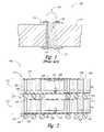
- FIG. 1illustrates an earlier interconnect 100 including a plugged via 110 .
- the via 110is formed by drilling or etching a hole through an interposer substrate 112 .
- the interconnectis then formed by plating a conductive material 114 into the via 110 , and patterning the conductive material 114 so that it is electrically isolated.
- the remaining void in the via 110is filled with a conductive material 116 that plugs the via 110 .
- the conductive material 114electrically connects a pad 117 at a first side of the package with a solder ball 1 18 (or other conductive feature) at a second side of the package.
- One challenge associated with the interconnect 100 in FIG. 1is the difficulty of achieving uniform metallization in the vias.
- Non-uniform plating within the viasdecreases the quality and integrity of the interconnect.
- vias having a high aspect ratioi.e., ratio of the depth to the size of the opening
- the filling processcan trap air in the via that can cause the interconnect or assembly to crack as the fill material and the assembly harden.
- Such non-uniformities in the viasprovide inconsistent electrical connections and compromise the integrity of the metallization of the interconnects.
- FIG. 1is a side cross-sectional view of a portion of an interconnect in an interposer substrate in accordance with the prior art.
- FIG. 2is a side cross-sectional view of a stacked semiconductor assembly in accordance with an embodiment of the invention.
- FIGS. 3-8are side cross-sectional views illustrating various stages in a method of forming interconnects in a packaged semiconductor assembly in accordance with embodiments of the invention.
- FIG. 9is flow diagram of a process of forming a semiconductor assembly in accordance with still another embodiment of the invention.
- FIGS. 10A and 10Bare side cross-sectional views illustrating various stages in a method of forming interconnects in a packaged semiconductor assembly in accordance with still another embodiment of the invention.
- FIGS. 11A-11Care side cross-sectional views illustrating various stages in a method of forming interconnects in a packaged semiconductor assembly in accordance with still another embodiment of the invention.
- FIG. 12is a flow diagram of a process of forming an interconnect in a packaged assembly in accordance with still another embodiment of the invention.
- FIG. 13is a schematic view of a system that incorporates packaged assemblies with interconnects in accordance with embodiments of the invention.
- FIGS. 2-13Several embodiments of the present invention are directed toward packaged semiconductor devices with interconnects and methods of forming interconnects in packaged semiconductor devices. Many specific details of the invention are described below with reference to methods of forming the interconnects.
- semiconductor assemblyis used throughout to include a variety of articles of manufacture including, for example, semiconductor wafers having active components, individual integrated circuit dies, packaged dies, and two or more semiconductor devices or assemblies in a stacked configuration. Many specific details of certain embodiments of the invention are set forth in FIGS. 2-13 and the following text to provide a thorough understanding of these embodiments.
- FIGS. 2-13Many specific details of certain embodiments of the invention are set forth in FIGS. 2-13 and the following text to provide a thorough understanding of these embodiments.
- FIGS. 2-13Several other embodiments of the invention can have different configurations, components or processes than those described in this section. A person skilled in the art, therefore, will appreciate that the invention may have additional embodiments or that the invention may be practiced without several details of the embodiments shown in FIG
- FIG. 2is a side cross-sectional view of a stacked semiconductor assembly 200 in accordance with one embodiment of the invention.
- the assembly 200includes two or more packaged semiconductor assemblies 210 in a stacked configuration.
- each assembly 210includes a microelectronic die 220 attached to a support layer 230 , and a plurality of interconnects 240 retained in and projecting from the support layer 230 in a predetermined configuration.
- the interconnects 240can comprise a plurality of preformed pin-like members or other pre-formed conductive structures.
- Individual assemblies 210also include an encapsulant 250 molded over the die 220 and between the interconnects 240 .
- each assembly 210can further include optional first and second redistribution structures 260 and 270 at opposite sides of the package, and a plurality of conductive members 280 attached to the first redistribution layer 260 .
- the interconnects 240can (a) provide high quality through package interconnections, (b) be formed relatively quickly, and (c) simplify the processing steps.
- individual interconnects 240are preformed pins or pin-like members extending from a first side 211 of the package to a second side 212 of the package.
- the pre-formed pinsprovide a uniform electrical connection through the package 210 without requiring the complex processes of forming, plating and filling vias through a package as in conventional interconnects.
- the interconnects 240are pre-formed in a separate process and then retained in a desired configuration before encapsulating the die 220 with the encapsulant 250 .
- the interconnects 240can be composed of a conductive material such as copper, nickel, gold and/or silver, or any other suitable conductive material(s).
- interconnects 240can also have a generally cylindrical shape and are all approximately the same size. In certain embodiments however, the interconnects 240 may differ in size or shape according to the needs and application of the packaged assembly.
- the interconnects 240typically have a diameter of 100 ⁇ m or more, although in certain embodiments the diameter may be less.
- the interconnects 240are inserted into the support layer 230 , a plate (not shown), or another type of support member in a predetermined configuration or array. Thereafter, the support layer 230 (or plate) retains the interconnects 240 in the desired configuration while the encapsulant 250 is molded around the interconnects 240 and the die 220 .
- the interconnects 240provide a continuous and uniform conductive structure through the encapsulation 250 and avoid some of the complexities associated with forming, plating and filling vias of conventional interconnects described above.
- FIGS. 3-8illustrate various stages in a method of forming a plurality of discrete arrays of the interconnects 240 of FIG. 2 in accordance with one embodiment of the invention.
- FIG. 3more specifically, illustrates a stage in which a plurality of discrete arrays of interconnects 240 have been mounted to a support plate 214 in a desired configuration.
- the interconnects 240can be mounted to the support plate 214 by loading the preformed interconnects 240 into a socket 208 that releasably retains second portions 244 of the interconnects 240 (shown in broken lines).
- the socket 208moves towards the plate 214 (arrows 209 ) to insert first portions 242 of individual interconnects 240 into corresponding recesses 216 in the plate 214 .
- the second portions 244 of the interconnects 240are free-standing without a solid material between the second portions 244 at this stage.
- the plurality of interconnects 240are at least substantially simultaneously mounted to the plate 214 .
- the interconnects 240can be mounted to the plate 214 individually.
- the recesses 216can be precision machined holes arranged in a predetermined array corresponding to an interconnect array at a die site of the semiconductor assembly. Such precision machining can enable the recesses 216 to be arranged in a dense array.
- the first portions 242can optionally have a beveled or pointed portion 243 to facilitate inserting the interconnects 240 in the recesses 216 .
- the lower portion of the plate 214is sufficiently thick so that the recesses 216 have a sufficient depth to retain the interconnects 240 in a desired configuration during subsequent processing steps.
- the interconnects 240can be ultrasonically welded or otherwise adhered to the plate 214 , and therefore the plate 214 in such embodiments does not need to have the recesses 216 .
- the plate 214can be composed of a metal or a synthetic material, such as an epoxy.
- an epoxy plateit can include the recesses 216 or the epoxy can be partially cured to provide a “self-embedding” plate such that the interconnects 240 can be inserted into the plate 214 without any preformed holes.
- the epoxy plate 214can be further cured or hardened. This type of self-embedding epoxy plate may mitigate errors caused by misalignment between the interconnects 240 and the recesses 216 in a rigid plate.
- the procedure illustrated in FIG. 3can be performed in a short period of time because the plurality of interconnects 240 can be formed and arranged off-line and then simultaneously mounted to the plate 214 in a single step. This reduces the number of processing steps and thus the processing time.
- the socket 208can be a device similar to a test socket or test probe, as is known in the art for electrical testing of packaged assemblies, and used to simultaneously insert multiple interconnects 240 into the plate 214 . Moreover, the insertion process can be automated using existing technologies.
- FIG. 4illustrates a stage in which a dielectric support layer 230 is formed or otherwise disposed in a cavity 215 of the plate 214 and around the interconnects 240 .
- the support layer 230 in FIG. 4has a first surface 232 contacting the plate 214 , and a second surface 234 spaced apart from the first surface 232 .
- the support layer 230can be a polymer disposed in the cavity 215 to surround each of the interconnects 240 . Accordingly, the thickness of the support layer 230 can vary according to the depth of the cavity 215 or how much the cavity 215 is filled with the support layer 230 .
- the support layer 230provides a dielectric material between the conductive interconnects 240 , and the support layer 230 can also retain the first portions 242 of the interconnects 240 in the desired configuration.
- the support layer 230can be at least partially cured or hardened to hold the interconnects 240 in a desired configuration during subsequent molding and material removal steps.
- the support layer 230can be disposed in the cavity 215 before the interconnects 240 are inserted into the plate 214 .
- the interconnects 240are inserted through the support layer 230 and into the individual recesses 216 in the plate 214 before curing the support layer 230 .
- the support layer 230can also provide a surface to which a plurality of dies can be mounted.
- the support layer 230can be a polymeric material in which the second surface 234 becomes tacky in a partially or fully cured state, or a separate adhesive layer can be applied to the second surface 234 . Accordingly, individual dies can be securely attached to the second surface 234 of the support layer 230 .
- the support layer 230can also be a photoimageable polymer that can be patterned to open bond-sites or conductive features on the die.
- FIG. 5illustrates a stage in which a plurality of semiconductor dies 220 have been attached to the second surface 234 of the support layer 230 .
- the active surfaces of individual dies 220are adhered to the second surface 234 of the support layer 230 .
- the support layer 230also provides a passivation or protective layer on the active surfaces of the dies 220 .
- the support layer 230can be deformable at this state so that optional conductive members 228 can project from bond-sites 222 of the dies 220 into the support layer 230 .
- the conductive member 228can be a stud ump formed on the die 220 before the die 220 is attached to the support layer 230 .
- the die 220can include other bond-sites or electrically connective features, or that the backside of the die 220 can be attached to the support layer 230 .
- FIG. 6illustrates a stage in which the encapsulation 250 has been disposed around the components of the sub-assemblies 210 to form a semiconductor workpiece 213 .
- the encapsulant 250can be composed of a different materials, such as thermosets, thermoplastics, hybridized versions of thermosets and thermoplastics, or any other suitable encapsulating material.
- the subassembly of the plate 214 , interconnects 240 and dies 220is positioned in a mold (not shown), and the encapsulant 250 is then molded between the interconnects 240 and over the dies 220 such that the encapsulant 250 at least partially covers each of the dies 220 .
- the moldcan be shaped like a conventional semiconductor wafer so that subsequent processes can be performed in wafer processing equipment.
- the plate 214 and support layer 230support and retain the interconnects 240 in the predetermined array during the molding process.
- the encapsulantalso protects the dies 220 from contamination (e.g., moisture, particulates, etc.) and electrically isolates the interconnects 240 .
- the thickness of the encapsulant 250can vary with respect to the length of the interconnects 240 .
- the surface of the encapsulant 250can be co-planar with the second portions 244 of the interconnects 240 after molding as indicated by the portion 252 of the encapsulant 250 .
- the second portions 244 of the interconnects 240can be completely over-molded with the encapsulant 250 as indicated by the broken line and the portion 254 of the encapsulant 250 . Material removal steps explained below are also used to adjust the thickness of the encapsulant 250 and surface characteristics of the workpiece 213 .
- FIG. 7illustrates a stage in which material has been removed from opposite surfaces of the workpiece 213 .
- the workpiece 213is ground, planarized and/or etched to remove the material from a first surface 290 of the workpiece 213 .
- the first surface 290can be formed by removing the material portions of the plate 214 and the support layer 230 to expose the first portions 242 of the interconnects 240 .
- a portion 217 of the plate 214can remain with the workpiece 213 even though the lower portion of the plate 214 has been removed.
- a portion of the support layer 230can also remain to provide a dielectric passivation layer at the surface of the die 220 .
- materialcan be removed from the workpiece 213 until the conductive members 228 are also exposed.
- a second surface 292 of the workpiece 213can be ground, planarized and/or etched to remove a portion of the encapsulant 250 from the workpiece 213 . This process can remove a portion of the second portions 244 of the interconnects 240 and expose or clean the second portions 244 of the pins. Accordingly, the thickness 256 of the workpiece 213 can be controlled by accurately forming the first and second surfaces 290 and 292 .
- FIG. 8is cross-sectional view of the assembly 210 after a first redistribution structure 260 has been formed at the first side 290 of the workpiece 213 , and a second redistribution structure 270 has been formed at the second side 292 of the workpiece 213 .
- the first and second redistribution structures 260 and 270can be configured to electrically connect the bond-sites 222 of the dies 220 to one or more of the interconnects 240 .
- the support layer 230is patterned to expose the bond-sites 222 , and then bumps, balls, wire bonds or other conductive members are attached to the bond-sites 222 .
- a support layer 230composed of a photoimageable polymer can be patterned to expose the bond-sites 222 .
- the first redistribution structure 260electrically connects the conductive members 228 to one or more of the interconnects 240 .
- the assemblies 210 with interconnects 240can provide consistent electrical properties.
- the preformed interconnects 240can be formed off-line apart from the packaging process such that they are consistently solid and void-free.
- molding over the pre-inserted interconnects 240can be a fast and relatively cost effective method of forming the interconnects through the encapsulant 250 because the foregoing process eliminates the patterning, etching, plating and filling processing steps used in conventional processes for forming interconnects.
- individual dies 220can have additional bond-sites or active surfaces proximate to the second surface 292 of the package 210 .
- the second redistribution structure 270can also electrically connect to the die 220 to the second surface 292 of the package 210 .
- a plurality of conductive featuressuch as the solder balls illustrated in FIG. 2 , may also be attached to and project from the first and second redistribution structures 260 and 270 .
- the sub-assemblies 210can be singulated from the workpiece 213 . In certain embodiments, for example, the sub-assemblies can be singulated with a wafer saw or other singulating devices that are known in the art.
- FIG. 9is a flow diagram of an embodiment of a method or process 900 for forming a semiconductor assembly.
- the process 900includes mounting preformed interconnect structures to a plate in a predetermined array of interconnects for the assembly (block 905 ).
- a socket holding a plurality of the interconnect structurescan simultaneously mount or insert the interconnect structures in apertures or recesses in the plate. Once the interconnect structures have been mounted, the socket can release the interconnect structures and move away from the plate.
- the platecan be made of a metallic or synthetic material, and the apertures or recesses can extend through the plate or to a predetermined depth of the plate.
- the processalso includes forming a dielectric support layer on the plate and around the interconnect structures (block 910 ) and positioning a die on the support layer ( 920 ).
- the processfurther includes encasing at least a portion of the plate, support layer, die and interconnect structures in an encapsulant (block 920 ).
- encasing the components of the assemblycan include forming a generally coplanar exterior surface of the encapsulant with second portions of the interconnect structures spaced apart from the support layer. In other embodiments, the second portions can be completely over-molded.
- the processalso includes exposing portions of the interconnect structures (block 925 ). In certain embodiments, exposing these portions can include planarizing first and second sides of the assembly to expose the interconnect structures.
- the platecan be a sacrificial layer and at least partially removed during the planarization. Exposing these portions in other embodiments can also include forming a generally coplanar first and second surfaces of the assembly with first and second portions of the interconnect structures.
- the process illustrated in FIG. 9can be accomplished in a short period of time because individual vias do not have to be formed, plated and filled to create the interconnect structures. Rather, the encapsulant encases the interconnects or pins after the pins have been retained in the predetermined array.
- FIGS. 10A and 10Billustrate various stages in a method for forming interconnects in a semiconductor assembly in accordance with another embodiment of the invention.
- FIG. 10Ais a side cross-sectional view of an embodiment of the invention having a plate 314 similar to the plate described above, except that the plate 314 can be removed from the sub-assembly or workpiece.
- the plate 314releasably receives the plurality of the interconnects 240 in a plurality of recesses 316 arranged in a predetermined interconnect array. Individual recesses 316 , however, do not extend all the way through the plate 314 .
- the pin 240when the first portion 242 of a pin 240 is inserted in the recess 316 , the pin 240 does not extend to a lower surface 317 of the plate 314 .
- the first portions 242 of the pins 240can be configured to have a semi-blunt end portion, such as a dowel-like first portion 242 illustrated in FIGS. 10A and 10B .
- the plate 314also includes a cavity 315 for receiving the support layer 230 . After forming the support layer 330 in the cavity 315 , processing can continue as described above with respect to FIGS. 5 and 6 , including attaching a plurality of dies 220 to the support layer 330 and disposing the encapsulant 250 around the interconnects 240 and dies 220 .
- FIG. 10Billustrates a stage in which an encapsulant 250 has been disposed around the interconnects 240 and dies 220 , and the plate 314 has been removed from the support layer 330 and interconnects 240 .
- processingcan continue as described above with respect to FIGS. 7-8 , including removing material and forming redistribution structures.
- the removable plate 314 illustrated in FIGS. 10A and 10Bcan save material cost and processing time because the material removal steps (e.g., planarizing) will not have to remove the plate 314 with the other package materials.
- the removable plate 314can also be reused for other semiconductor assemblies having the same interconnect configuration.
- FIGS. 11A-11Cillustrate various stages in a method for forming interconnects in a semiconductor assembly according to still another embodiment of the invention.
- the manufacturing process and interconnects illustrated in FIGS. 11A-11Chave similar features to the embodiments described above, however the first portions 242 of the interconnects 240 are retained solely by a support layer 430 and not inserted into a separate support plate.
- FIGS. 11A and 11Billustrate a stage in which the interconnects 240 are temporarily retained by a socket 402 and inserted into the support layer 430 .
- the support layer 430can be a polymer, and at the stage shown in FIGS. 11A and 11B the support layer is in a state in which the interconnects can penetrate the support layer 430 .
- the first portions 242 of the interconnects 240can have different configurations, such as the beveled or pointed first portions 243 , flat portions 245 (shown at the right of FIG. 11A ), or other configurations suitable for embedding and retaining the interconnects 240 in a stable manner. While the socket 402 holds the interconnects 240 in a desired configuration, the support layer 430 can be at least partially cured or otherwise processed to retain the interconnects 240 in the desired configuration. The socket 402 subsequently releases the second portions 244 of the interconnects ( FIG. 11C ) and the support layer 430 holds the interconnects 240 in place.
- the second portions 244 of the interconnects 240are free-standing without a solid material between the second portions 244 .
- the support layer 430can also provide an adhesive surface 434 to which a die (not shown) can be attached as described above.
- FIGS. 11A-11Cretains the interconnects 240 in a desired configuration in the support layer 430 without inserting the first portions 242 of the interconnects 240 into holes in a separate plate. Accordingly, this embodiment may mitigate the need to align the interconnects 240 with holes or recesses in a separate support plate.
- FIG. 12is a flow diagram of an embodiment of a method or process 1200 for forming an interconnect.
- the process 1200includes inserting a plurality of preformed pins in a support member (block 1205 ).
- the support membercan at least partially retain the pins in a predetermined array.
- the pinscan include a first portion in the support member and a second portion opposite the first portion.
- the plurality of pinscan be simultaneously inserted in the support member.
- a socketholds the second portions of the pins, inserts the first portions of the pins in the support member in the predetermined array, and releases the second portions after the first portions are inserted and retained in the support member.
- the processalso includes positioning a die on a first surface of the support member (block 1210 ).
- the processcan include at least partially curing the support member prior to positioning the die on the support layer.
- the processfurther includes encasing at least a portion of the die and pins with an encapsulant (block 1215 ) and at least partially exposing the pins (block 1220 ).
- any one of the semiconductor assemblies having the interconnects described above with reference to FIGS. 1-12can be incorporated into any of a myriad of larger and/or more complex systems, a representative example of which is system 1300 shown schematically in FIG. 13 .
- the system 1300can include a processor 1302 , a memory 1304 (e.g., SRAM, DRAM, flash and/or other memory devices), input/output devices 1306 and/or other subsystems or components 1308 .
- the semiconductor assemblies having interconnects described above with reference to FIGS. 1-12may be included in any of the components shown in FIG. 13 .
- the resulting system 1300can perform any of a wide variety of computing, processing, storage, sensing, imaging and/or other functions.
- the representative systems 1300include, without limitation, computers and/or other data processors, for example, desktop computers, laptop computers, Internet appliances, hand-held devices (e.g., palm-top computers, wearable computers, cellular or mobile phones, personal digital assistants, music players, etc.), multi-processor systems, processor-based or programmable consumer electronics, network computers and minicomputers.
- Other representative systems 1300may be housed in a single unit or distributed over multiple interconnected units (e.g., through a communication network).
- the components of the system 1300can accordingly include local and/or remote memory storage devices, and any of a wide variety of computer readable media.
- the backside of the dies 220can be mounted to the support layer 230 such that the bond-sites 222 face away from the support layer 220 .
- the bond-sites 222can be protected during the molding procedure such that they are not covered by the encapsulant 250 , and then the bond-sites 222 can be electrically connected to corresponding interconnects (e.g., via wire bonding or redistribution structure).
- interconnectse.g., via wire bonding or redistribution structure
Landscapes
- Engineering & Computer Science (AREA)
- Microelectronics & Electronic Packaging (AREA)
- Power Engineering (AREA)
- Computer Hardware Design (AREA)
- Physics & Mathematics (AREA)
- Condensed Matter Physics & Semiconductors (AREA)
- General Physics & Mathematics (AREA)
- Ceramic Engineering (AREA)
- Manufacturing & Machinery (AREA)
- Encapsulation Of And Coatings For Semiconductor Or Solid State Devices (AREA)
- Led Device Packages (AREA)
- Structures Or Materials For Encapsulating Or Coating Semiconductor Devices Or Solid State Devices (AREA)
Abstract
Description
- The present invention relates to interconnects for packaged semiconductor assemblies, stacked semiconductor assemblies, and methods for manufacturing such assemblies.
- Semiconductor products require packaged semiconductor assemblies with a high density of devices in a relatively small space. For example, the space available for memory devices, processors, displays and other microfeature devices is continually decreasing in cell phones, personal digital assistants, laptop computers and many other products. One technique to increase the density of semiconductor devices within a given footprint is to stack semiconductor devices and assemblies, and many stacked semiconductor assemblies require adequate electrical interconnects within and between the packages.
- Conventional interconnects electrically connect the integrated circuitry of a semiconductor device (such as a die) with other devices or stacked packages. These interconnects can be formed by creating a via in the packaging material and then filling or plugging the via with conductive material.
FIG. 1 illustrates anearlier interconnect 100 including a plugged via110. Thevia 110 is formed by drilling or etching a hole through aninterposer substrate 112. The interconnect is then formed by plating aconductive material 114 into thevia 110, and patterning theconductive material 114 so that it is electrically isolated. The remaining void in thevia 110 is filled with aconductive material 116 that plugs thevia 110. Theconductive material 114 electrically connects apad 117 at a first side of the package with a solder ball118 (or other conductive feature) at a second side of the package. - One challenge associated with the
interconnect 100 inFIG. 1 is the difficulty of achieving uniform metallization in the vias. Non-uniform plating within the vias decreases the quality and integrity of the interconnect. For example, vias having a high aspect ratio (i.e., ratio of the depth to the size of the opening) are especially difficult to consistently plate and fill. Moreover, in certain circumstances the filling process can trap air in the via that can cause the interconnect or assembly to crack as the fill material and the assembly harden. Such non-uniformities in the vias provide inconsistent electrical connections and compromise the integrity of the metallization of the interconnects. - Other challenges associated with existing interconnects are the cost, time and complexity of forming, plating and filling the vias. Forming the vias by an ablation or drilling process typically requires forming individual vias in a sequential manner: this increases the processing time to form the vias. Simultaneously forming the vias by an etching process can be much faster, but etching can result in inconsistent sizes of the vias. It can also be difficult to achieve a dense distribution of the vias with an etching process. Moreover, the plating and filling processing steps following the via formation require additional processing time.
FIG. 1 is a side cross-sectional view of a portion of an interconnect in an interposer substrate in accordance with the prior art.FIG. 2 is a side cross-sectional view of a stacked semiconductor assembly in accordance with an embodiment of the invention.FIGS. 3-8 are side cross-sectional views illustrating various stages in a method of forming interconnects in a packaged semiconductor assembly in accordance with embodiments of the invention.FIG. 9 is flow diagram of a process of forming a semiconductor assembly in accordance with still another embodiment of the invention.FIGS. 10A and 10B are side cross-sectional views illustrating various stages in a method of forming interconnects in a packaged semiconductor assembly in accordance with still another embodiment of the invention.FIGS. 11A-11C are side cross-sectional views illustrating various stages in a method of forming interconnects in a packaged semiconductor assembly in accordance with still another embodiment of the invention.FIG. 12 is a flow diagram of a process of forming an interconnect in a packaged assembly in accordance with still another embodiment of the invention.FIG. 13 is a schematic view of a system that incorporates packaged assemblies with interconnects in accordance with embodiments of the invention.- Several embodiments of the present invention are directed toward packaged semiconductor devices with interconnects and methods of forming interconnects in packaged semiconductor devices. Many specific details of the invention are described below with reference to methods of forming the interconnects. The term “semiconductor assembly” is used throughout to include a variety of articles of manufacture including, for example, semiconductor wafers having active components, individual integrated circuit dies, packaged dies, and two or more semiconductor devices or assemblies in a stacked configuration. Many specific details of certain embodiments of the invention are set forth in
FIGS. 2-13 and the following text to provide a thorough understanding of these embodiments. Several other embodiments of the invention can have different configurations, components or processes than those described in this section. A person skilled in the art, therefore, will appreciate that the invention may have additional embodiments or that the invention may be practiced without several details of the embodiments shown inFIGS. 2-13 . FIG. 2 is a side cross-sectional view of astacked semiconductor assembly 200 in accordance with one embodiment of the invention. Theassembly 200 includes two or more packagedsemiconductor assemblies 210 in a stacked configuration. In this embodiment, eachassembly 210 includes amicroelectronic die 220 attached to asupport layer 230, and a plurality ofinterconnects 240 retained in and projecting from thesupport layer 230 in a predetermined configuration. Theinterconnects 240 can comprise a plurality of preformed pin-like members or other pre-formed conductive structures.Individual assemblies 210 also include anencapsulant 250 molded over the die220 and between theinterconnects 240. In the illustrated embodiment, eachassembly 210 can further include optional first andsecond redistribution structures conductive members 280 attached to thefirst redistribution layer 260. As explained in more detail below, theinterconnects 240 can (a) provide high quality through package interconnections, (b) be formed relatively quickly, and (c) simplify the processing steps.- In the embodiment shown in
FIG. 2 ,individual interconnects 240 are preformed pins or pin-like members extending from afirst side 211 of the package to asecond side 212 of the package. The pre-formed pins provide a uniform electrical connection through thepackage 210 without requiring the complex processes of forming, plating and filling vias through a package as in conventional interconnects. Instead of forming and filling vias, theinterconnects 240 are pre-formed in a separate process and then retained in a desired configuration before encapsulating thedie 220 with theencapsulant 250. In certain embodiments, theinterconnects 240 can be composed of a conductive material such as copper, nickel, gold and/or silver, or any other suitable conductive material(s).Individual interconnects 240 can also have a generally cylindrical shape and are all approximately the same size. In certain embodiments however, theinterconnects 240 may differ in size or shape according to the needs and application of the packaged assembly. Theinterconnects 240 typically have a diameter of 100 μm or more, although in certain embodiments the diameter may be less. As explained in more detail below, theinterconnects 240 are inserted into thesupport layer 230, a plate (not shown), or another type of support member in a predetermined configuration or array. Thereafter, the support layer230 (or plate) retains theinterconnects 240 in the desired configuration while theencapsulant 250 is molded around theinterconnects 240 and thedie 220. As such, theinterconnects 240 provide a continuous and uniform conductive structure through theencapsulation 250 and avoid some of the complexities associated with forming, plating and filling vias of conventional interconnects described above. FIGS. 3-8 illustrate various stages in a method of forming a plurality of discrete arrays of theinterconnects 240 ofFIG. 2 in accordance with one embodiment of the invention.FIG. 3 , more specifically, illustrates a stage in which a plurality of discrete arrays ofinterconnects 240 have been mounted to asupport plate 214 in a desired configuration. Theinterconnects 240 can be mounted to thesupport plate 214 by loading thepreformed interconnects 240 into asocket 208 that releasably retainssecond portions 244 of the interconnects240 (shown in broken lines). In operation, thesocket 208 moves towards the plate214 (arrows209) to insertfirst portions 242 ofindividual interconnects 240 intocorresponding recesses 216 in theplate 214. Thesecond portions 244 of theinterconnects 240 are free-standing without a solid material between thesecond portions 244 at this stage. In this manner, the plurality ofinterconnects 240 are at least substantially simultaneously mounted to theplate 214. In certain embodiments, theinterconnects 240 can be mounted to theplate 214 individually. Therecesses 216 can be precision machined holes arranged in a predetermined array corresponding to an interconnect array at a die site of the semiconductor assembly. Such precision machining can enable therecesses 216 to be arranged in a dense array. Thefirst portions 242 can optionally have a beveled or pointedportion 243 to facilitate inserting theinterconnects 240 in therecesses 216. The lower portion of theplate 214 is sufficiently thick so that therecesses 216 have a sufficient depth to retain theinterconnects 240 in a desired configuration during subsequent processing steps. In certain embodiments, theinterconnects 240 can be ultrasonically welded or otherwise adhered to theplate 214, and therefore theplate 214 in such embodiments does not need to have therecesses 216.- The
plate 214 can be composed of a metal or a synthetic material, such as an epoxy. In the case of an epoxy plate, it can include therecesses 216 or the epoxy can be partially cured to provide a “self-embedding” plate such that theinterconnects 240 can be inserted into theplate 214 without any preformed holes. Once theinterconnects 240 are in place, theepoxy plate 214 can be further cured or hardened. This type of self-embedding epoxy plate may mitigate errors caused by misalignment between theinterconnects 240 and therecesses 216 in a rigid plate. - The procedure illustrated in
FIG. 3 can be performed in a short period of time because the plurality ofinterconnects 240 can be formed and arranged off-line and then simultaneously mounted to theplate 214 in a single step. This reduces the number of processing steps and thus the processing time. Thesocket 208 can be a device similar to a test socket or test probe, as is known in the art for electrical testing of packaged assemblies, and used to simultaneously insertmultiple interconnects 240 into theplate 214. Moreover, the insertion process can be automated using existing technologies. - After mounting the
interconnects 240 to theplate 214,FIG. 4 illustrates a stage in which adielectric support layer 230 is formed or otherwise disposed in acavity 215 of theplate 214 and around theinterconnects 240. Thesupport layer 230 inFIG. 4 has afirst surface 232 contacting theplate 214, and asecond surface 234 spaced apart from thefirst surface 232. In certain embodiments, thesupport layer 230 can be a polymer disposed in thecavity 215 to surround each of theinterconnects 240. Accordingly, the thickness of thesupport layer 230 can vary according to the depth of thecavity 215 or how much thecavity 215 is filled with thesupport layer 230. - The
support layer 230 provides a dielectric material between theconductive interconnects 240, and thesupport layer 230 can also retain thefirst portions 242 of theinterconnects 240 in the desired configuration. For example, thesupport layer 230 can be at least partially cured or hardened to hold theinterconnects 240 in a desired configuration during subsequent molding and material removal steps. In certain embodiments, thesupport layer 230 can be disposed in thecavity 215 before theinterconnects 240 are inserted into theplate 214. In this embodiment, theinterconnects 240 are inserted through thesupport layer 230 and into theindividual recesses 216 in theplate 214 before curing thesupport layer 230.0022 Thesupport layer 230 can also provide a surface to which a plurality of dies can be mounted. For example, thesupport layer 230 can be a polymeric material in which thesecond surface 234 becomes tacky in a partially or fully cured state, or a separate adhesive layer can be applied to thesecond surface 234. Accordingly, individual dies can be securely attached to thesecond surface 234 of thesupport layer 230. Moreover, in certain embodiments thesupport layer 230 can also be a photoimageable polymer that can be patterned to open bond-sites or conductive features on the die. FIG. 5 illustrates a stage in which a plurality of semiconductor dies220 have been attached to thesecond surface 234 of thesupport layer 230. In this embodiment, the active surfaces of individual dies220 are adhered to thesecond surface 234 of thesupport layer 230. Thesupport layer 230 also provides a passivation or protective layer on the active surfaces of the dies220. Thesupport layer 230 can be deformable at this state so that optionalconductive members 228 can project from bond-sites 222 of the dies220 into thesupport layer 230. In certain embodiments, theconductive member 228 can be a stud ump formed on thedie 220 before thedie 220 is attached to thesupport layer 230. One skilled in the art will appreciate that thedie 220 can include other bond-sites or electrically connective features, or that the backside of thedie 220 can be attached to thesupport layer 230.FIG. 6 illustrates a stage in which theencapsulation 250 has been disposed around the components of thesub-assemblies 210 to form asemiconductor workpiece 213. Theencapsulant 250 can be composed of a different materials, such as thermosets, thermoplastics, hybridized versions of thermosets and thermoplastics, or any other suitable encapsulating material. In one embodiment, the subassembly of theplate 214,interconnects 240 and dies220 is positioned in a mold (not shown), and theencapsulant 250 is then molded between theinterconnects 240 and over the dies220 such that theencapsulant 250 at least partially covers each of the dies220. The mold can be shaped like a conventional semiconductor wafer so that subsequent processes can be performed in wafer processing equipment. Theplate 214 andsupport layer 230 support and retain theinterconnects 240 in the predetermined array during the molding process. The encapsulant also protects the dies220 from contamination (e.g., moisture, particulates, etc.) and electrically isolates theinterconnects 240. The thickness of theencapsulant 250 can vary with respect to the length of theinterconnects 240. For example, in certain embodiments, the surface of theencapsulant 250 can be co-planar with thesecond portions 244 of theinterconnects 240 after molding as indicated by theportion 252 of theencapsulant 250. In other embodiments, thesecond portions 244 of theinterconnects 240 can be completely over-molded with theencapsulant 250 as indicated by the broken line and theportion 254 of theencapsulant 250. Material removal steps explained below are also used to adjust the thickness of theencapsulant 250 and surface characteristics of theworkpiece 213.FIG. 7 illustrates a stage in which material has been removed from opposite surfaces of theworkpiece 213. In one embodiment, theworkpiece 213 is ground, planarized and/or etched to remove the material from afirst surface 290 of theworkpiece 213. Thefirst surface 290, for example, can be formed by removing the material portions of theplate 214 and thesupport layer 230 to expose thefirst portions 242 of theinterconnects 240. Aportion 217 of theplate 214 can remain with theworkpiece 213 even though the lower portion of theplate 214 has been removed. A portion of thesupport layer 230 can also remain to provide a dielectric passivation layer at the surface of thedie 220. In the embodiments where the dies220 includeconductive members 228, material can be removed from theworkpiece 213 until theconductive members 228 are also exposed. In an optional embodiment, asecond surface 292 of theworkpiece 213 can be ground, planarized and/or etched to remove a portion of the encapsulant250 from theworkpiece 213. This process can remove a portion of thesecond portions 244 of theinterconnects 240 and expose or clean thesecond portions 244 of the pins. Accordingly, thethickness 256 of theworkpiece 213 can be controlled by accurately forming the first andsecond surfaces FIG. 8 is cross-sectional view of theassembly 210 after afirst redistribution structure 260 has been formed at thefirst side 290 of theworkpiece 213, and asecond redistribution structure 270 has been formed at thesecond side 292 of theworkpiece 213. The first andsecond redistribution structures sites 222 of the dies220 to one or more of theinterconnects 240. In embodiments withoutconductive members 228 projecting from thedie 220, thesupport layer 230 is patterned to expose the bond-sites 222, and then bumps, balls, wire bonds or other conductive members are attached to the bond-sites 222. For example, asupport layer 230 composed of a photoimageable polymer can be patterned to expose the bond-sites 222. In embodiments whereconductive members 228 project from thedie 220 and are exposed by the material removal processes, thefirst redistribution structure 260 electrically connects theconductive members 228 to one or more of theinterconnects 240.- Several embodiments of the
assemblies 210 withinterconnects 240 can provide consistent electrical properties. For example, the preformedinterconnects 240 can be formed off-line apart from the packaging process such that they are consistently solid and void-free. Additionally, molding over thepre-inserted interconnects 240 can be a fast and relatively cost effective method of forming the interconnects through theencapsulant 250 because the foregoing process eliminates the patterning, etching, plating and filling processing steps used in conventional processes for forming interconnects. - One skilled in the art will appreciate that individual dies220 can have additional bond-sites or active surfaces proximate to the
second surface 292 of thepackage 210. Accordingly, in certain embodiments, thesecond redistribution structure 270 can also electrically connect to the die220 to thesecond surface 292 of thepackage 210. A plurality of conductive features, such as the solder balls illustrated inFIG. 2 , may also be attached to and project from the first andsecond redistribution structures redistribution structures sub-assemblies 210 can be singulated from theworkpiece 213. In certain embodiments, for example, the sub-assemblies can be singulated with a wafer saw or other singulating devices that are known in the art. FIG. 9 is a flow diagram of an embodiment of a method orprocess 900 for forming a semiconductor assembly. In this embodiment, theprocess 900 includes mounting preformed interconnect structures to a plate in a predetermined array of interconnects for the assembly (block905). In one embodiment, a socket holding a plurality of the interconnect structures can simultaneously mount or insert the interconnect structures in apertures or recesses in the plate. Once the interconnect structures have been mounted, the socket can release the interconnect structures and move away from the plate. The plate can be made of a metallic or synthetic material, and the apertures or recesses can extend through the plate or to a predetermined depth of the plate. The process also includes forming a dielectric support layer on the plate and around the interconnect structures (block910) and positioning a die on the support layer (920).- The process further includes encasing at least a portion of the plate, support layer, die and interconnect structures in an encapsulant (block920). In certain embodiments encasing the components of the assembly can include forming a generally coplanar exterior surface of the encapsulant with second portions of the interconnect structures spaced apart from the support layer. In other embodiments, the second portions can be completely over-molded. The process also includes exposing portions of the interconnect structures (block925). In certain embodiments, exposing these portions can include planarizing first and second sides of the assembly to expose the interconnect structures. As such, the plate can be a sacrificial layer and at least partially removed during the planarization. Exposing these portions in other embodiments can also include forming a generally coplanar first and second surfaces of the assembly with first and second portions of the interconnect structures.
- The process illustrated in
FIG. 9 can be accomplished in a short period of time because individual vias do not have to be formed, plated and filled to create the interconnect structures. Rather, the encapsulant encases the interconnects or pins after the pins have been retained in the predetermined array. FIGS. 10A and 10B illustrate various stages in a method for forming interconnects in a semiconductor assembly in accordance with another embodiment of the invention.FIG. 10A , more specifically, is a side cross-sectional view of an embodiment of the invention having aplate 314 similar to the plate described above, except that theplate 314 can be removed from the sub-assembly or workpiece. Theplate 314 releasably receives the plurality of theinterconnects 240 in a plurality ofrecesses 316 arranged in a predetermined interconnect array.Individual recesses 316, however, do not extend all the way through theplate 314. Accordingly, when thefirst portion 242 of apin 240 is inserted in therecess 316, thepin 240 does not extend to alower surface 317 of theplate 314. In certain embodiments, thefirst portions 242 of thepins 240 can be configured to have a semi-blunt end portion, such as a dowel-likefirst portion 242 illustrated inFIGS. 10A and 10B . Theplate 314 also includes acavity 315 for receiving thesupport layer 230. After forming thesupport layer 330 in thecavity 315, processing can continue as described above with respect toFIGS. 5 and 6 , including attaching a plurality of dies220 to thesupport layer 330 and disposing theencapsulant 250 around theinterconnects 240 and dies220.FIG. 10B illustrates a stage in which anencapsulant 250 has been disposed around theinterconnects 240 and dies220, and theplate 314 has been removed from thesupport layer 330 and interconnects240. After theplate 314 is removed, processing can continue as described above with respect toFIGS. 7-8 , including removing material and forming redistribution structures. Theremovable plate 314 illustrated inFIGS. 10A and 10B can save material cost and processing time because the material removal steps (e.g., planarizing) will not have to remove theplate 314 with the other package materials. Theremovable plate 314 can also be reused for other semiconductor assemblies having the same interconnect configuration.FIGS. 11A-11C illustrate various stages in a method for forming interconnects in a semiconductor assembly according to still another embodiment of the invention. The manufacturing process and interconnects illustrated inFIGS. 11A-11C have similar features to the embodiments described above, however thefirst portions 242 of theinterconnects 240 are retained solely by asupport layer 430 and not inserted into a separate support plate.FIGS. 11A and 11B , for example, illustrate a stage in which theinterconnects 240 are temporarily retained by asocket 402 and inserted into thesupport layer 430. Thesupport layer 430 can be a polymer, and at the stage shown inFIGS. 11A and 11B the support layer is in a state in which the interconnects can penetrate thesupport layer 430. In certain embodiments, thefirst portions 242 of theinterconnects 240 can have different configurations, such as the beveled or pointedfirst portions 243, flat portions245 (shown at the right ofFIG. 11A ), or other configurations suitable for embedding and retaining theinterconnects 240 in a stable manner. While thesocket 402 holds theinterconnects 240 in a desired configuration, thesupport layer 430 can be at least partially cured or otherwise processed to retain theinterconnects 240 in the desired configuration. Thesocket 402 subsequently releases thesecond portions 244 of the interconnects (FIG. 11C ) and thesupport layer 430 holds theinterconnects 240 in place. At this stage, thesecond portions 244 of the interconnects240 (e.g., pins) are free-standing without a solid material between thesecond portions 244. Thesupport layer 430 can also provide anadhesive surface 434 to which a die (not shown) can be attached as described above.- The embodiment illustrated in
FIGS. 11A-11C retains theinterconnects 240 in a desired configuration in thesupport layer 430 without inserting thefirst portions 242 of theinterconnects 240 into holes in a separate plate. Accordingly, this embodiment may mitigate the need to align theinterconnects 240 with holes or recesses in a separate support plate. FIG. 12 is a flow diagram of an embodiment of a method orprocess 1200 for forming an interconnect. Theprocess 1200 includes inserting a plurality of preformed pins in a support member (block1205). The support member can at least partially retain the pins in a predetermined array. The pins can include a first portion in the support member and a second portion opposite the first portion. Moreover, the plurality of pins can be simultaneously inserted in the support member. In one example, a socket holds the second portions of the pins, inserts the first portions of the pins in the support member in the predetermined array, and releases the second portions after the first portions are inserted and retained in the support member. The process also includes positioning a die on a first surface of the support member (block1210). In certain embodiments, the process can include at least partially curing the support member prior to positioning the die on the support layer. The process further includes encasing at least a portion of the die and pins with an encapsulant (block1215) and at least partially exposing the pins (block1220).- Any one of the semiconductor assemblies having the interconnects described above with reference to
FIGS. 1-12 can be incorporated into any of a myriad of larger and/or more complex systems, a representative example of which issystem 1300 shown schematically inFIG. 13 . Thesystem 1300 can include aprocessor 1302, a memory1304 (e.g., SRAM, DRAM, flash and/or other memory devices), input/output devices 1306 and/or other subsystems orcomponents 1308. The semiconductor assemblies having interconnects described above with reference toFIGS. 1-12 may be included in any of the components shown inFIG. 13 . The resultingsystem 1300 can perform any of a wide variety of computing, processing, storage, sensing, imaging and/or other functions. Accordingly, therepresentative systems 1300 include, without limitation, computers and/or other data processors, for example, desktop computers, laptop computers, Internet appliances, hand-held devices (e.g., palm-top computers, wearable computers, cellular or mobile phones, personal digital assistants, music players, etc.), multi-processor systems, processor-based or programmable consumer electronics, network computers and minicomputers. Otherrepresentative systems 1300 may be housed in a single unit or distributed over multiple interconnected units (e.g., through a communication network). The components of thesystem 1300 can accordingly include local and/or remote memory storage devices, and any of a wide variety of computer readable media. - From the foregoing, it will be appreciated that specific embodiments of the invention have been described herein for purposes of illustration, but well-known structures and functions have not been shown or described in detail to avoid unnecessarily obscuring the description of the embodiments of the invention. For example, the backside of the dies220 can be mounted to the
support layer 230 such that the bond-sites 222 face away from thesupport layer 220. The bond-sites 222 can be protected during the molding procedure such that they are not covered by theencapsulant 250, and then the bond-sites 222 can be electrically connected to corresponding interconnects (e.g., via wire bonding or redistribution structure). Where the context permits, singular or plural terms may also include the plural or singular term, respectively. Moreover, unless the word “or” is expressly limited to mean only a single item exclusive from the other items in reference to a list of two or more items, then the use of “or” in such a list is to be interpreted as including (a) any single item in the list, (b) all of the items in the list, or (c) any combination of the items in the list. Additionally, the term “comprising” is used throughout to mean including at least the recited feature(s) such that any greater number of the same feature and/or additional types of features are not precluded. - Various modifications may be made without deviating from the embodiments of the invention. For example, features described in the context of particular embodiments may be combined or eliminated in other embodiments. Further, while advantages associated with certain embodiments of the invention have been described in the context of those embodiments, other embodiments may also exhibit such advantages, and not all embodiments need necessarily exhibit such advantages to fall within the scope of the invention. For example, the interconnect structures (e.g., pins) can be retained by another type of support member before molding the encapsulant around the die and interconnects. Accordingly, the invention is not limited except as by the appended claims.
Claims (34)
Priority Applications (2)
| Application Number | Priority Date | Filing Date | Title |
|---|---|---|---|
| US12/875,958US8168476B2 (en) | 2007-07-12 | 2010-09-03 | Interconnects for packaged semiconductor devices and methods for manufacturing such devices |
| US13/459,801US8445330B2 (en) | 2007-07-12 | 2012-04-30 | Interconnects for packaged semiconductor devices and methods for manufacturing such devices |
Applications Claiming Priority (2)
| Application Number | Priority Date | Filing Date | Title |
|---|---|---|---|
| SG200705178-2ASG149710A1 (en) | 2007-07-12 | 2007-07-12 | Interconnects for packaged semiconductor devices and methods for manufacturing such devices |
| SG200705178-2 | 2007-07-12 |
Related Child Applications (1)
| Application Number | Title | Priority Date | Filing Date |
|---|---|---|---|
| US12/875,958DivisionUS8168476B2 (en) | 2007-07-12 | 2010-09-03 | Interconnects for packaged semiconductor devices and methods for manufacturing such devices |
Publications (2)
| Publication Number | Publication Date |
|---|---|
| US20090014859A1true US20090014859A1 (en) | 2009-01-15 |
| US7791203B2 US7791203B2 (en) | 2010-09-07 |
Family
ID=39677732
Family Applications (3)
| Application Number | Title | Priority Date | Filing Date |
|---|---|---|---|
| US11/848,836Expired - Fee RelatedUS7791203B2 (en) | 2007-07-12 | 2007-08-31 | Interconnects for packaged semiconductor devices and methods for manufacturing such devices |
| US12/875,958ActiveUS8168476B2 (en) | 2007-07-12 | 2010-09-03 | Interconnects for packaged semiconductor devices and methods for manufacturing such devices |
| US13/459,801ActiveUS8445330B2 (en) | 2007-07-12 | 2012-04-30 | Interconnects for packaged semiconductor devices and methods for manufacturing such devices |
Family Applications After (2)
| Application Number | Title | Priority Date | Filing Date |
|---|---|---|---|
| US12/875,958ActiveUS8168476B2 (en) | 2007-07-12 | 2010-09-03 | Interconnects for packaged semiconductor devices and methods for manufacturing such devices |
| US13/459,801ActiveUS8445330B2 (en) | 2007-07-12 | 2012-04-30 | Interconnects for packaged semiconductor devices and methods for manufacturing such devices |
Country Status (4)
| Country | Link |
|---|---|
| US (3) | US7791203B2 (en) |
| SG (1) | SG149710A1 (en) |
| TW (1) | TWI442542B (en) |
| WO (1) | WO2009009588A1 (en) |
Cited By (44)
| Publication number | Priority date | Publication date | Assignee | Title |
|---|---|---|---|---|
| US7629249B2 (en) | 2006-08-28 | 2009-12-08 | Micron Technology, Inc. | Microfeature workpieces having conductive interconnect structures formed by chemically reactive processes, and associated systems and methods |
| US20100052183A1 (en)* | 2005-09-01 | 2010-03-04 | Micron Technology, Inc. | Microfeature workpiece substrates having through-substrate vias, and associated methods of formation |
| US7683458B2 (en) | 2004-09-02 | 2010-03-23 | Micron Technology, Inc. | Through-wafer interconnects for photoimager and memory wafers |
| US20100148337A1 (en)* | 2008-12-17 | 2010-06-17 | Yong Liu | Stackable semiconductor package and process to manufacture same |
| US7749899B2 (en) | 2006-06-01 | 2010-07-06 | Micron Technology, Inc. | Microelectronic workpieces and methods and systems for forming interconnects in microelectronic workpieces |
| US20100216410A1 (en)* | 2009-02-20 | 2010-08-26 | Aiconn Technology Corporation | Radio transceiver module |
| US7795134B2 (en) | 2005-06-28 | 2010-09-14 | Micron Technology, Inc. | Conductive interconnect structures and formation methods using supercritical fluids |
| US20100237495A1 (en)* | 2009-03-17 | 2010-09-23 | Stats Chippac, Ltd. | Semiconductor Device and Method of Providing Z-Interconnect Conductive Pillars with Inner Polymer Core |
| US20100258946A1 (en)* | 2009-04-10 | 2010-10-14 | Shinko Electric Industries Co., Ltd. | Semiconductor device, manufacturing method thereof, and electronic device |
| US20100258927A1 (en)* | 2009-04-10 | 2010-10-14 | Sanka Ganesan | Package-on-package interconnect stiffener |
| US7830018B2 (en) | 2007-08-31 | 2010-11-09 | Micron Technology, Inc. | Partitioned through-layer via and associated systems and methods |
| US7829976B2 (en) | 2004-06-29 | 2010-11-09 | Micron Technology, Inc. | Microelectronic devices and methods for forming interconnects in microelectronic devices |
| US20100330749A1 (en)* | 2007-07-12 | 2010-12-30 | Micron Technology, Inc. | Interconnects for packaged semiconductor devices and methods for manufacturing such devices |
| US7863187B2 (en) | 2005-09-01 | 2011-01-04 | Micron Technology, Inc. | Microfeature workpieces and methods for forming interconnects in microfeature workpieces |
| US7884015B2 (en) | 2007-12-06 | 2011-02-08 | Micron Technology, Inc. | Methods for forming interconnects in microelectronic workpieces and microelectronic workpieces formed using such methods |
| US7902643B2 (en) | 2006-08-31 | 2011-03-08 | Micron Technology, Inc. | Microfeature workpieces having interconnects and conductive backplanes, and associated systems and methods |
| US20110057308A1 (en)* | 2009-09-10 | 2011-03-10 | Daesik Choi | Integrated circuit packaging system with conductive pillars and method of manufacture thereof |
| US7915736B2 (en) | 2005-09-01 | 2011-03-29 | Micron Technology, Inc. | Microfeature workpieces and methods for forming interconnects in microfeature workpieces |
| US20110156264A1 (en)* | 2009-12-24 | 2011-06-30 | Shinko Electric Industries Co., Ltd. | Semiconductor element built-in device |
| US8084854B2 (en) | 2007-12-28 | 2011-12-27 | Micron Technology, Inc. | Pass-through 3D interconnect for microelectronic dies and associated systems and methods |
| US8084866B2 (en) | 2003-12-10 | 2011-12-27 | Micron Technology, Inc. | Microelectronic devices and methods for filling vias in microelectronic devices |
| US8253230B2 (en) | 2008-05-15 | 2012-08-28 | Micron Technology, Inc. | Disabling electrical connections using pass-through 3D interconnects and associated systems and methods |
| US8322031B2 (en) | 2004-08-27 | 2012-12-04 | Micron Technology, Inc. | Method of manufacturing an interposer |
| US8536485B2 (en) | 2004-05-05 | 2013-09-17 | Micron Technology, Inc. | Systems and methods for forming apertures in microfeature workpieces |
| US8623711B2 (en)* | 2011-12-15 | 2014-01-07 | Stats Chippac Ltd. | Integrated circuit packaging system with package-on-package and method of manufacture thereof |
| US8629567B2 (en) | 2011-12-15 | 2014-01-14 | Stats Chippac Ltd. | Integrated circuit packaging system with contacts and method of manufacture thereof |
| CN103797577A (en)* | 2011-09-07 | 2014-05-14 | 株式会社村田制作所 | Method for producing module and terminal assembly |
| CN103828043A (en)* | 2011-09-07 | 2014-05-28 | 株式会社村田制作所 | Module manufacturing method and module |
| US8742598B2 (en)* | 2011-10-05 | 2014-06-03 | Infineon Technologies Ag | Semiconductor structure and method for making same |
| CN103915414A (en)* | 2012-12-31 | 2014-07-09 | 英特尔移动通信有限责任公司 | Flip-chip wafer level package and methods thereof |
| US20150181708A1 (en)* | 2013-12-20 | 2015-06-25 | Samsung Electro-Mechanics Co., Ltd. | Semiconductor package module |
| US20150201497A1 (en)* | 2009-12-16 | 2015-07-16 | Intel Corporation | High-density inter-package connections for ultra-thin package-on-package structures, and processes of forming same |
| US9219029B2 (en) | 2011-12-15 | 2015-12-22 | Stats Chippac Ltd. | Integrated circuit packaging system with terminals and method of manufacture thereof |
| US9263361B2 (en) | 2006-11-10 | 2016-02-16 | Stats Chippac, Ltd. | Semiconductor device having a vertical interconnect structure using stud bumps |
| US9373585B2 (en)* | 2014-09-17 | 2016-06-21 | Invensas Corporation | Polymer member based interconnect |
| US9385074B2 (en) | 2006-11-10 | 2016-07-05 | STATS ChipPAC Pte. Ltd. | Semiconductor package with embedded die |
| CN105870023A (en)* | 2014-12-27 | 2016-08-17 | 矽品精密工业股份有限公司 | Package structure and method for fabricating the same |
| CN106601626A (en)* | 2016-12-21 | 2017-04-26 | 江苏长电科技股份有限公司 | Process of producing three-dimensional system-level circuit board through packaging, etching, copper column electroplating and conduction |
| US9666514B2 (en)* | 2015-04-14 | 2017-05-30 | Invensas Corporation | High performance compliant substrate |
| US20170207172A1 (en)* | 2016-01-15 | 2017-07-20 | Samsung Electro-Mechanics Co., Ltd. | Electronic component package and method of manufacturing the same |
| US20170317020A1 (en)* | 2016-04-29 | 2017-11-02 | Nxp Usa, Inc. | Appartus and methods for multi-die packaging |
| US9831206B2 (en)* | 2014-03-28 | 2017-11-28 | Intel Corporation | LPS solder paste based low cost fine pitch pop interconnect solutions |
| US20170374738A1 (en)* | 2015-01-22 | 2017-12-28 | Invensas Corporation | Interposers And Fabrication Methods That Use Nanoparticle Inks And Magnetic Fields |
| US10658333B2 (en)* | 2018-07-31 | 2020-05-19 | Taiwan Semiconductor Manufacturing Co., Ltd. | Package structure and method of fabricating the same |
Families Citing this family (18)
| Publication number | Priority date | Publication date | Assignee | Title |
|---|---|---|---|---|
| US7651889B2 (en)* | 2007-09-13 | 2010-01-26 | Freescale Semiconductor, Inc. | Electromagnetic shield formation for integrated circuit die package |
| JP5081578B2 (en)* | 2007-10-25 | 2012-11-28 | ローム株式会社 | Resin-sealed semiconductor device |
| US8198547B2 (en) | 2009-07-23 | 2012-06-12 | Lexmark International, Inc. | Z-directed pass-through components for printed circuit boards |
| JP5574639B2 (en)* | 2009-08-21 | 2014-08-20 | 三菱電機株式会社 | Semiconductor device and manufacturing method thereof |
| US9078374B2 (en) | 2011-08-31 | 2015-07-07 | Lexmark International, Inc. | Screening process for manufacturing a Z-directed component for a printed circuit board |
| US20130341078A1 (en)* | 2012-06-20 | 2013-12-26 | Keith Bryan Hardin | Z-directed printed circuit board components having a removable end portion and methods therefor |
| US8943684B2 (en) | 2011-08-31 | 2015-02-03 | Lexmark International, Inc. | Continuous extrusion process for manufacturing a Z-directed component for a printed circuit board |
| US9009954B2 (en) | 2011-08-31 | 2015-04-21 | Lexmark International, Inc. | Process for manufacturing a Z-directed component for a printed circuit board using a sacrificial constraining material |
| JP5984526B2 (en)* | 2012-06-20 | 2016-09-06 | 日本電波工業株式会社 | Surface mount device |
| US9646899B2 (en) | 2012-09-13 | 2017-05-09 | Micron Technology, Inc. | Interconnect assemblies with probed bond pads |
| CN103400810A (en)* | 2013-06-28 | 2013-11-20 | 三星半导体(中国)研究开发有限公司 | Semiconductor chip laminating and packaging structure and manufacturing method thereof |
| KR20150033979A (en)* | 2013-09-25 | 2015-04-02 | 삼성전기주식회사 | Interposer board and method of manufacturing the same |
| CN104332456A (en)* | 2014-09-04 | 2015-02-04 | 华进半导体封装先导技术研发中心有限公司 | Wafer-level fan-out stacked packaging structure and manufacturing process thereof |
| US9337064B2 (en) | 2014-09-15 | 2016-05-10 | Micron Technology, Inc. | Methods of protecting peripheries of in-process semiconductor wafers and related in-process wafers and systems |
| CN105097565B (en)* | 2015-06-30 | 2018-01-30 | 通富微电子股份有限公司 | The forming method of encapsulating structure |
| US9859253B1 (en)* | 2016-06-29 | 2018-01-02 | Intel Corporation | Integrated circuit package stack |
| US10700011B2 (en)* | 2016-12-07 | 2020-06-30 | STATS ChipPAC Pte. Ltd. | Semiconductor device and method of forming an integrated SIP module with embedded inductor or package |
| CN114446910B (en)* | 2020-10-30 | 2024-09-10 | 京东方科技集团股份有限公司 | Chip structure, packaging structure, manufacturing method of chip structure and binding method |
Citations (77)
| Publication number | Priority date | Publication date | Assignee | Title |
|---|---|---|---|---|
| US5006922A (en)* | 1990-02-14 | 1991-04-09 | Motorola, Inc. | Packaged semiconductor device having a low cost ceramic PGA package |
| US5098864A (en)* | 1989-11-29 | 1992-03-24 | Olin Corporation | Process for manufacturing a metal pin grid array package |
| US5102829A (en)* | 1991-07-22 | 1992-04-07 | At&T Bell Laboratories | Plastic pin grid array package |
| US5144412A (en)* | 1987-02-19 | 1992-09-01 | Olin Corporation | Process for manufacturing plastic pin grid arrays and the product produced thereby |
| US5145099A (en)* | 1990-07-13 | 1992-09-08 | Micron Technology, Inc. | Method for combining die attach and lead bond in the assembly of a semiconductor package |
| US5200366A (en)* | 1990-04-27 | 1993-04-06 | Hitachi, Ltd. | Semiconductor device, its fabrication method and molding apparatus used therefor |
| US5291062A (en)* | 1993-03-01 | 1994-03-01 | Motorola, Inc. | Area array semiconductor device having a lid with functional contacts |
| US5485039A (en)* | 1991-12-27 | 1996-01-16 | Hitachi, Ltd. | Semiconductor substrate having wiring conductors at a first main surface electrically connected to plural pins at a second main surface |
| US5550403A (en)* | 1994-06-02 | 1996-08-27 | Lsi Logic Corporation | Improved laminate package for an integrated circuit and integrated circuit having such a package |
| US5726493A (en)* | 1994-06-13 | 1998-03-10 | Fujitsu Limited | Semiconductor device and semiconductor device unit having ball-grid-array type package structure |
| US5734555A (en)* | 1994-03-30 | 1998-03-31 | Intel Corporation | Shared socket multi-chip module and/or piggyback pin grid array package |
| US5776824A (en)* | 1995-12-22 | 1998-07-07 | Micron Technology, Inc. | Method for producing laminated film/metal structures for known good die ("KG") applications |
| US5821532A (en)* | 1997-06-16 | 1998-10-13 | Eastman Kodak Company | Imager package substrate |
| US5851845A (en)* | 1995-12-18 | 1998-12-22 | Micron Technology, Inc. | Process for packaging a semiconductor die using dicing and testing |
| US6008070A (en)* | 1998-05-21 | 1999-12-28 | Micron Technology, Inc. | Wafer level fabrication and assembly of chip scale packages |
| US6097087A (en)* | 1997-10-31 | 2000-08-01 | Micron Technology, Inc. | Semiconductor package including flex circuit, interconnects and dense array external contacts |
| US6103547A (en)* | 1997-01-17 | 2000-08-15 | Micron Technology, Inc. | High speed IC package configuration |
| US6114240A (en)* | 1997-12-18 | 2000-09-05 | Micron Technology, Inc. | Method for fabricating semiconductor components using focused laser beam |
| US6124634A (en)* | 1996-03-07 | 2000-09-26 | Micron Technology, Inc. | Micromachined chip scale package |
| US6137163A (en)* | 1997-09-12 | 2000-10-24 | Hyundai Electronics Industries Co., Ltd. | Semiconductor substrate and stackable semiconductor package and fabrication method thereof |
| US6159764A (en)* | 1997-07-02 | 2000-12-12 | Micron Technology, Inc. | Varied-thickness heat sink for integrated circuit (IC) packages and method of fabricating IC packages |
| US6184465B1 (en)* | 1998-11-12 | 2001-02-06 | Micron Technology, Inc. | Semiconductor package |
| US6222270B1 (en)* | 1997-06-24 | 2001-04-24 | Samsung Electronics Co., Ltd. | Integrated circuit bonding pads including closed vias and closed conductive patterns |
| US6228687B1 (en)* | 1999-06-28 | 2001-05-08 | Micron Technology, Inc. | Wafer-level package and methods of fabricating |
| US6229202B1 (en)* | 2000-01-10 | 2001-05-08 | Micron Technology, Inc. | Semiconductor package having downset leadframe for reducing package bow |
| US6246108B1 (en)* | 1997-09-15 | 2001-06-12 | Micron Technology, Inc. | Integrated circuit package including lead frame with electrically isolated alignment feature |
| US6271580B1 (en)* | 1996-12-30 | 2001-08-07 | Micron Technology, Inc. | Leads under chip in conventional IC package |
| US6291894B1 (en)* | 1998-08-31 | 2001-09-18 | Micron Technology, Inc. | Method and apparatus for a semiconductor package for vertical surface mounting |
| US6294837B1 (en)* | 1997-12-18 | 2001-09-25 | Micron Technology, Inc. | Semiconductor interconnect having laser machined contacts |
| US6448106B1 (en)* | 1999-11-09 | 2002-09-10 | Fujitsu Limited | Modules with pins and methods for making modules with pins |
| US20030042564A1 (en)* | 2000-12-04 | 2003-03-06 | Fujitsu Limited | Semiconductor device having an interconnecting post formed on an interposer within a sealing resin |
| US6576531B2 (en)* | 2001-08-24 | 2003-06-10 | Micron Technology, Inc. | Method for cutting semiconductor wafers |
| US6582992B2 (en)* | 2001-11-16 | 2003-06-24 | Micron Technology, Inc. | Stackable semiconductor package and wafer level fabrication method |
| US6620731B1 (en)* | 1997-12-18 | 2003-09-16 | Micron Technology, Inc. | Method for fabricating semiconductor components and interconnects with contacts on opposing sides |
| US20030216023A1 (en)* | 1997-03-26 | 2003-11-20 | Wark James M. | Projected contact structures for engaging bumped semiconductor devices and methods of making the same |
| US20040004280A1 (en)* | 2002-07-04 | 2004-01-08 | Manabu Shibata | Semiconductor device and system having semiconductor device mounted thereon |
| US6774486B2 (en)* | 2001-10-10 | 2004-08-10 | Micron Technology, Inc. | Circuit boards containing vias and methods for producing same |
| US20040178491A1 (en)* | 1997-12-18 | 2004-09-16 | Salman Akram | Method for fabricating semiconductor components by forming conductive members using solder |
| US20040198033A1 (en)* | 2002-08-20 | 2004-10-07 | Lee Teck Kheng | Double bumping of flexible substrate for first and second level interconnects |
| US6809025B2 (en)* | 1997-02-18 | 2004-10-26 | Micron Technology, Inc. | Method of making a void-free aluminum film |
| US20040219763A1 (en)* | 2002-02-20 | 2004-11-04 | Kim Sarah E. | Process of vertically stacking multiple wafers supporting different active integrated circuit (IC) devices |
| US6828175B2 (en)* | 2002-08-29 | 2004-12-07 | Micron Technology, Inc. | Semiconductor component with backside contacts and method of fabrication |
| US6847109B2 (en)* | 2002-09-25 | 2005-01-25 | Samsung Electronics Co., Ltd. | Area array semiconductor package and 3-dimensional stack thereof |
| US6858891B2 (en)* | 2002-03-06 | 2005-02-22 | Micron Technology, Inc. | Nanotube semiconductor devices and methods for making the same |
| US6885107B2 (en)* | 2002-08-29 | 2005-04-26 | Micron Technology, Inc. | Flip-chip image sensor packages and methods of fabrication |
| US20050104228A1 (en)* | 2003-11-13 | 2005-05-19 | Rigg Sidney B. | Microelectronic devices, methods for forming vias in microelectronic devices, and methods for packaging microelectronic devices |
| US20050110889A1 (en)* | 2003-11-26 | 2005-05-26 | Tuttle Mark E. | Packaged microelectronic imagers and methods of packaging microelectronic imagers |
| US20050127478A1 (en)* | 2003-12-10 | 2005-06-16 | Hiatt William M. | Microelectronic devices and methods for filling vias in microelectronic devices |
| US20050150683A1 (en)* | 2004-01-12 | 2005-07-14 | Farnworth Warren M. | Methods of fabricating substrates and substrate precursor structures resulting therefrom |
| US20050184219A1 (en)* | 2004-02-23 | 2005-08-25 | Kirby Kyle K. | Packaged microelectronic imagers and methods of packaging microelectronic imagers |
| US6946325B2 (en)* | 2003-03-14 | 2005-09-20 | Micron Technology, Inc. | Methods for packaging microelectronic devices |
| US20050208766A1 (en)* | 2004-03-19 | 2005-09-22 | Kirby Kyle K | Etch solution for selectively removing silicon and methods of selectively removing silicon |
| US20050227382A1 (en)* | 2004-04-02 | 2005-10-13 | Hui Angela T | In-situ surface treatment for memory cell formation |
| US20050236708A1 (en)* | 2004-04-27 | 2005-10-27 | Farnworth Warren M | Microelectronic imaging devices and methods of packaging microelectronic imaging devices |
| US20050247894A1 (en)* | 2004-05-05 | 2005-11-10 | Watkins Charles M | Systems and methods for forming apertures in microfeature workpieces |
| US20050253213A1 (en)* | 2004-05-13 | 2005-11-17 | Tongbi Jiang | Covers for microelectronic imagers and methods for wafer-level packaging of microelectronics imagers |
| US20050254133A1 (en)* | 2004-05-13 | 2005-11-17 | Salman Akram | Integrated optics units and methods of manufacturing integrated optics units for use with microelectronic imagers |
| US20050258530A1 (en)* | 2004-04-13 | 2005-11-24 | Al Vindasius | Micropede stacked die component assembly |
| US20050275051A1 (en)* | 2004-06-14 | 2005-12-15 | Farnworth Warren M | Prefabricated housings for microelectronic imagers and methods for packaging microelectronic imagers |
| US20050277293A1 (en)* | 2004-06-15 | 2005-12-15 | Kim Soon-Bum | Fabrication method of wafer level chip scale packages |
| US20050275750A1 (en)* | 2004-06-09 | 2005-12-15 | Salman Akram | Wafer-level packaged microelectronic imagers and processes for wafer-level packaging |
| US20050275048A1 (en)* | 2004-06-14 | 2005-12-15 | Farnworth Warren M | Microelectronic imagers and methods of packaging microelectronic imagers |
| US20050282374A1 (en)* | 2004-06-22 | 2005-12-22 | Samsung Electronics Co., Ltd. | Method of forming a thin wafer stack for a wafer level package |
| US6982487B2 (en)* | 2003-03-25 | 2006-01-03 | Samsung Electronics Co., Ltd. | Wafer level package and multi-package stack |
| US20060038272A1 (en)* | 2004-08-17 | 2006-02-23 | Texas Instruments Incorporated | Stacked wafer scale package |
| US20060046468A1 (en)* | 2004-08-31 | 2006-03-02 | Salman Akram | Through-substrate interconnect fabrication methods and resulting structures and assemblies |
| US20060057776A1 (en)* | 2004-09-10 | 2006-03-16 | Advanced Semiconductor Engineering Inc. | Wafer stacking package method |
| US20060057836A1 (en)* | 2004-09-10 | 2006-03-16 | Agency For Science, Technology And Research | Method of stacking thin substrates by transfer bonding |
| US20060255443A1 (en)* | 2005-05-10 | 2006-11-16 | Samsung Electronics Co., Ltd. | Multi stack packaging chip and method of manufacturing the same |
| US7151009B2 (en)* | 2004-06-18 | 2006-12-19 | Samsung Electronics Co., Ltd. | Method for manufacturing wafer level chip stack package |
| US20070012655A1 (en)* | 2005-07-15 | 2007-01-18 | Samsung Electronics Co., Ltd. | Micro-package, multi-stack micro-package, and manufacturing method therefor |
| US7170183B1 (en)* | 2005-05-13 | 2007-01-30 | Amkor Technology, Inc. | Wafer level stacked package |
| US20070023121A1 (en)* | 2005-07-29 | 2007-02-01 | Freescale Semiconductor, Inc. | Fabrication of three dimensional integrated circuit employing multiple die panels |
| US20070045779A1 (en)* | 2005-09-01 | 2007-03-01 | Hiatt W M | Methods for forming through-wafer interconnects, intermediate structures so formed, and devices and systems having at least one solder dam structure |
| US20070045806A1 (en)* | 2004-02-05 | 2007-03-01 | United Microelectronics Corp. | Structure of an ultra-thin wafer level stack package |
| US20070122940A1 (en)* | 2005-11-30 | 2007-05-31 | Viswanadam Gautham | Method for packaging a semiconductor device |
| US20070145563A1 (en)* | 2005-12-28 | 2007-06-28 | Punzalan Nelson V | Stacked packages with interconnecting pins |
Family Cites Families (67)
| Publication number | Priority date | Publication date | Assignee | Title |
|---|---|---|---|---|
| US4907127A (en)* | 1988-03-21 | 1990-03-06 | Lee John K C | Printed circuit board construction and method for producing printed circuit end products |
| NL9300971A (en) | 1993-06-04 | 1995-01-02 | Framatome Connectors Belgium | Circuit board connector assembly. |
| KR100565961B1 (en) | 1999-08-21 | 2006-03-30 | 삼성전자주식회사 | 3D stacked chip package manufacturing method |
| WO2001015223A1 (en) | 1999-08-23 | 2001-03-01 | Rohm Co., Ltd. | Semiconductor device and method of manufacture thereof |
| US6682955B2 (en) | 2002-05-08 | 2004-01-27 | Micron Technology, Inc. | Stacked die module and techniques for forming a stacked die module |
| KR20040017037A (en)* | 2002-08-20 | 2004-02-26 | 삼성전자주식회사 | Semiconductor contact structure and method of forming the same |
| KR100444588B1 (en) | 2002-11-12 | 2004-08-16 | 삼성전자주식회사 | Fabrication of via hole for glass wafer |
| KR100482180B1 (en) | 2002-12-16 | 2005-04-14 | 동부아남반도체 주식회사 | Fabricating method of semiconductor device |
| KR100621991B1 (en) | 2003-01-03 | 2006-09-13 | 삼성전자주식회사 | Chip Scale Stacking Package |
| US6841883B1 (en) | 2003-03-31 | 2005-01-11 | Micron Technology, Inc. | Multi-dice chip scale semiconductor components and wafer level methods of fabrication |
| KR100537892B1 (en)* | 2003-08-26 | 2005-12-21 | 삼성전자주식회사 | Chip stack package and manufacturing method thereof |
| US7498647B2 (en) | 2004-06-10 | 2009-03-03 | Micron Technology, Inc. | Packaged microelectronic imagers and methods of packaging microelectronic imagers |
| US7232754B2 (en) | 2004-06-29 | 2007-06-19 | Micron Technology, Inc. | Microelectronic devices and methods for forming interconnects in microelectronic devices |
| US7416913B2 (en) | 2004-07-16 | 2008-08-26 | Micron Technology, Inc. | Methods of manufacturing microelectronic imaging units with discrete standoffs |
| US7189954B2 (en) | 2004-07-19 | 2007-03-13 | Micron Technology, Inc. | Microelectronic imagers with optical devices and methods of manufacturing such microelectronic imagers |
| US7402453B2 (en) | 2004-07-28 | 2008-07-22 | Micron Technology, Inc. | Microelectronic imaging units and methods of manufacturing microelectronic imaging units |
| US20060023107A1 (en) | 2004-08-02 | 2006-02-02 | Bolken Todd O | Microelectronic imagers with optics supports having threadless interfaces and methods for manufacturing such microelectronic imagers |
| US7364934B2 (en) | 2004-08-10 | 2008-04-29 | Micron Technology, Inc. | Microelectronic imaging units and methods of manufacturing microelectronic imaging units |
| US7645635B2 (en) | 2004-08-16 | 2010-01-12 | Micron Technology, Inc. | Frame structure and semiconductor attach process for use therewith for fabrication of image sensor packages and the like, and resulting packages |
| US7632747B2 (en) | 2004-08-19 | 2009-12-15 | Micron Technology, Inc. | Conductive structures for microfeature devices and methods for fabricating microfeature devices |
| US7223626B2 (en) | 2004-08-19 | 2007-05-29 | Micron Technology, Inc. | Spacers for packaged microelectronic imagers and methods of making and using spacers for wafer-level packaging of imagers |
| US7397066B2 (en) | 2004-08-19 | 2008-07-08 | Micron Technology, Inc. | Microelectronic imagers with curved image sensors and methods for manufacturing microelectronic imagers |
| US7425499B2 (en) | 2004-08-24 | 2008-09-16 | Micron Technology, Inc. | Methods for forming interconnects in vias and microelectronic workpieces including such interconnects |
| US7199050B2 (en) | 2004-08-24 | 2007-04-03 | Micron Technology, Inc. | Pass through via technology for use during the manufacture of a semiconductor device |
| US7429494B2 (en) | 2004-08-24 | 2008-09-30 | Micron Technology, Inc. | Microelectronic imagers with optical devices having integral reference features and methods for manufacturing such microelectronic imagers |
| US7115961B2 (en) | 2004-08-24 | 2006-10-03 | Micron Technology, Inc. | Packaged microelectronic imaging devices and methods of packaging microelectronic imaging devices |
| US7276393B2 (en) | 2004-08-26 | 2007-10-02 | Micron Technology, Inc. | Microelectronic imaging units and methods of manufacturing microelectronic imaging units |
| SG120200A1 (en) | 2004-08-27 | 2006-03-28 | Micron Technology Inc | Slanted vias for electrical circuits on circuit boards and other substrates |
| US7378342B2 (en) | 2004-08-27 | 2008-05-27 | Micron Technology, Inc. | Methods for forming vias varying lateral dimensions |
| US7419852B2 (en) | 2004-08-27 | 2008-09-02 | Micron Technology, Inc. | Low temperature methods of forming back side redistribution layers in association with through wafer interconnects, semiconductor devices including same, and assemblies |
| US7511262B2 (en) | 2004-08-30 | 2009-03-31 | Micron Technology, Inc. | Optical device and assembly for use with imaging dies, and wafer-label imager assembly |
| US7244663B2 (en) | 2004-08-31 | 2007-07-17 | Micron Technology, Inc. | Wafer reinforcement structure and methods of fabrication |
| US7129567B2 (en) | 2004-08-31 | 2006-10-31 | Micron Technology, Inc. | Substrate, semiconductor die, multichip module, and system including a via structure comprising a plurality of conductive elements |
| US7646075B2 (en) | 2004-08-31 | 2010-01-12 | Micron Technology, Inc. | Microelectronic imagers having front side contacts |
| US7300857B2 (en) | 2004-09-02 | 2007-11-27 | Micron Technology, Inc. | Through-wafer interconnects for photoimager and memory wafers |
| US7271482B2 (en) | 2004-12-30 | 2007-09-18 | Micron Technology, Inc. | Methods for forming interconnects in microelectronic workpieces and microelectronic workpieces formed using such methods |
| US7303931B2 (en) | 2005-02-10 | 2007-12-04 | Micron Technology, Inc. | Microfeature workpieces having microlenses and methods of forming microlenses on microfeature workpieces |
| US20060177999A1 (en) | 2005-02-10 | 2006-08-10 | Micron Technology, Inc. | Microelectronic workpieces and methods for forming interconnects in microelectronic workpieces |
| US7190039B2 (en) | 2005-02-18 | 2007-03-13 | Micron Technology, Inc. | Microelectronic imagers with shaped image sensors and methods for manufacturing microelectronic imagers |
| US7371676B2 (en) | 2005-04-08 | 2008-05-13 | Micron Technology, Inc. | Method for fabricating semiconductor components with through wire interconnects |
| US7425507B2 (en) | 2005-06-28 | 2008-09-16 | Micron Technology, Inc. | Semiconductor substrates including vias of nonuniform cross section, methods of forming and associated structures |
| US20060290001A1 (en) | 2005-06-28 | 2006-12-28 | Micron Technology, Inc. | Interconnect vias and associated methods of formation |
| US7795134B2 (en) | 2005-06-28 | 2010-09-14 | Micron Technology, Inc. | Conductive interconnect structures and formation methods using supercritical fluids |
| US7429529B2 (en) | 2005-08-05 | 2008-09-30 | Farnworth Warren M | Methods of forming through-wafer interconnects and structures resulting therefrom |
| US7845540B2 (en) | 2005-08-30 | 2010-12-07 | Micron Technology, Inc. | Systems and methods for depositing conductive material into openings in microfeature workpieces |
| DE102005042074A1 (en) | 2005-08-31 | 2007-03-08 | Forschungsverbund Berlin E.V. | Method for producing plated-through holes in semiconductor wafers |
| US20070045812A1 (en) | 2005-08-31 | 2007-03-01 | Micron Technology, Inc. | Microfeature assemblies including interconnect structures and methods for forming such interconnect structures |
| US8308053B2 (en) | 2005-08-31 | 2012-11-13 | Micron Technology, Inc. | Microfeature workpieces having alloyed conductive structures, and associated methods |
| US7326591B2 (en) | 2005-08-31 | 2008-02-05 | Micron Technology, Inc. | Interconnecting substrates for microelectronic dies, methods for forming vias in such substrates, and methods for packaging microelectronic devices |
| US7517798B2 (en) | 2005-09-01 | 2009-04-14 | Micron Technology, Inc. | Methods for forming through-wafer interconnects and structures resulting therefrom |
| US7452743B2 (en) | 2005-09-01 | 2008-11-18 | Aptina Imaging Corporation | Microelectronic imaging units and methods of manufacturing microelectronic imaging units at the wafer level |
| US7863187B2 (en) | 2005-09-01 | 2011-01-04 | Micron Technology, Inc. | Microfeature workpieces and methods for forming interconnects in microfeature workpieces |
| US7262134B2 (en) | 2005-09-01 | 2007-08-28 | Micron Technology, Inc. | Microfeature workpieces and methods for forming interconnects in microfeature workpieces |
| US7622377B2 (en) | 2005-09-01 | 2009-11-24 | Micron Technology, Inc. | Microfeature workpiece substrates having through-substrate vias, and associated methods of formation |
| US7288757B2 (en) | 2005-09-01 | 2007-10-30 | Micron Technology, Inc. | Microelectronic imaging devices and associated methods for attaching transmissive elements |
| KR100753415B1 (en) | 2006-03-17 | 2007-08-30 | 주식회사 하이닉스반도체 | Stack package |
| US7648856B2 (en) | 2006-08-28 | 2010-01-19 | Micron Technology, Inc. | Methods for attaching microfeature dies to external devices |
| US7629249B2 (en) | 2006-08-28 | 2009-12-08 | Micron Technology, Inc. | Microfeature workpieces having conductive interconnect structures formed by chemically reactive processes, and associated systems and methods |
| US8021981B2 (en) | 2006-08-30 | 2011-09-20 | Micron Technology, Inc. | Redistribution layers for microfeature workpieces, and associated systems and methods |
| US7902643B2 (en) | 2006-08-31 | 2011-03-08 | Micron Technology, Inc. | Microfeature workpieces having interconnects and conductive backplanes, and associated systems and methods |
| KR100831405B1 (en) | 2006-10-02 | 2008-05-21 | (주) 파이오닉스 | Wafer Bonding Packaging Method |
| US8221557B2 (en) | 2007-07-06 | 2012-07-17 | Micron Technology, Inc. | Systems and methods for exposing semiconductor workpieces to vapors for through-hole cleaning and/or other processes |
| SG149710A1 (en)* | 2007-07-12 | 2009-02-27 | Micron Technology Inc | Interconnects for packaged semiconductor devices and methods for manufacturing such devices |
| SG150410A1 (en) | 2007-08-31 | 2009-03-30 | Micron Technology Inc | Partitioned through-layer via and associated systems and methods |
| US7884015B2 (en) | 2007-12-06 | 2011-02-08 | Micron Technology, Inc. | Methods for forming interconnects in microelectronic workpieces and microelectronic workpieces formed using such methods |
| US8084854B2 (en) | 2007-12-28 | 2011-12-27 | Micron Technology, Inc. | Pass-through 3D interconnect for microelectronic dies and associated systems and methods |
| US8253230B2 (en) | 2008-05-15 | 2012-08-28 | Micron Technology, Inc. | Disabling electrical connections using pass-through 3D interconnects and associated systems and methods |
- 2007
- 2007-07-12SGSG200705178-2Apatent/SG149710A1/enunknown
- 2007-08-31USUS11/848,836patent/US7791203B2/ennot_activeExpired - Fee Related
- 2008
- 2008-07-09WOPCT/US2008/069520patent/WO2009009588A1/enactiveApplication Filing
- 2008-07-11TWTW097126534Apatent/TWI442542B/enactive
- 2010
- 2010-09-03USUS12/875,958patent/US8168476B2/enactiveActive
- 2012
- 2012-04-30USUS13/459,801patent/US8445330B2/enactiveActive
Patent Citations (84)
| Publication number | Priority date | Publication date | Assignee | Title |
|---|---|---|---|---|
| US5144412A (en)* | 1987-02-19 | 1992-09-01 | Olin Corporation | Process for manufacturing plastic pin grid arrays and the product produced thereby |
| US5098864A (en)* | 1989-11-29 | 1992-03-24 | Olin Corporation | Process for manufacturing a metal pin grid array package |
| US5006922A (en)* | 1990-02-14 | 1991-04-09 | Motorola, Inc. | Packaged semiconductor device having a low cost ceramic PGA package |
| US5200366A (en)* | 1990-04-27 | 1993-04-06 | Hitachi, Ltd. | Semiconductor device, its fabrication method and molding apparatus used therefor |
| US5145099A (en)* | 1990-07-13 | 1992-09-08 | Micron Technology, Inc. | Method for combining die attach and lead bond in the assembly of a semiconductor package |
| US5102829A (en)* | 1991-07-22 | 1992-04-07 | At&T Bell Laboratories | Plastic pin grid array package |
| US5485039A (en)* | 1991-12-27 | 1996-01-16 | Hitachi, Ltd. | Semiconductor substrate having wiring conductors at a first main surface electrically connected to plural pins at a second main surface |
| US5291062A (en)* | 1993-03-01 | 1994-03-01 | Motorola, Inc. | Area array semiconductor device having a lid with functional contacts |
| US5734555A (en)* | 1994-03-30 | 1998-03-31 | Intel Corporation | Shared socket multi-chip module and/or piggyback pin grid array package |
| US5550403A (en)* | 1994-06-02 | 1996-08-27 | Lsi Logic Corporation | Improved laminate package for an integrated circuit and integrated circuit having such a package |
| US5726493A (en)* | 1994-06-13 | 1998-03-10 | Fujitsu Limited | Semiconductor device and semiconductor device unit having ball-grid-array type package structure |
| US5851845A (en)* | 1995-12-18 | 1998-12-22 | Micron Technology, Inc. | Process for packaging a semiconductor die using dicing and testing |
| US5776824A (en)* | 1995-12-22 | 1998-07-07 | Micron Technology, Inc. | Method for producing laminated film/metal structures for known good die ("KG") applications |
| US6124634A (en)* | 1996-03-07 | 2000-09-26 | Micron Technology, Inc. | Micromachined chip scale package |
| US6271580B1 (en)* | 1996-12-30 | 2001-08-07 | Micron Technology, Inc. | Leads under chip in conventional IC package |
| US6133622A (en)* | 1997-01-17 | 2000-10-17 | Micron Technology, Inc. | High speed IC package configuration |
| US6103547A (en)* | 1997-01-17 | 2000-08-15 | Micron Technology, Inc. | High speed IC package configuration |
| US6809025B2 (en)* | 1997-02-18 | 2004-10-26 | Micron Technology, Inc. | Method of making a void-free aluminum film |
| US20030216023A1 (en)* | 1997-03-26 | 2003-11-20 | Wark James M. | Projected contact structures for engaging bumped semiconductor devices and methods of making the same |
| US5821532A (en)* | 1997-06-16 | 1998-10-13 | Eastman Kodak Company | Imager package substrate |
| US6222270B1 (en)* | 1997-06-24 | 2001-04-24 | Samsung Electronics Co., Ltd. | Integrated circuit bonding pads including closed vias and closed conductive patterns |
| US6159764A (en)* | 1997-07-02 | 2000-12-12 | Micron Technology, Inc. | Varied-thickness heat sink for integrated circuit (IC) packages and method of fabricating IC packages |
| US6137163A (en)* | 1997-09-12 | 2000-10-24 | Hyundai Electronics Industries Co., Ltd. | Semiconductor substrate and stackable semiconductor package and fabrication method thereof |
| US6246108B1 (en)* | 1997-09-15 | 2001-06-12 | Micron Technology, Inc. | Integrated circuit package including lead frame with electrically isolated alignment feature |
| US6097087A (en)* | 1997-10-31 | 2000-08-01 | Micron Technology, Inc. | Semiconductor package including flex circuit, interconnects and dense array external contacts |
| US6620731B1 (en)* | 1997-12-18 | 2003-09-16 | Micron Technology, Inc. | Method for fabricating semiconductor components and interconnects with contacts on opposing sides |
| US6114240A (en)* | 1997-12-18 | 2000-09-05 | Micron Technology, Inc. | Method for fabricating semiconductor components using focused laser beam |
| US6294837B1 (en)* | 1997-12-18 | 2001-09-25 | Micron Technology, Inc. | Semiconductor interconnect having laser machined contacts |
| US6903443B2 (en)* | 1997-12-18 | 2005-06-07 | Micron Technology, Inc. | Semiconductor component and interconnect having conductive members and contacts on opposing sides |
| US20040178491A1 (en)* | 1997-12-18 | 2004-09-16 | Salman Akram | Method for fabricating semiconductor components by forming conductive members using solder |
| US6008070A (en)* | 1998-05-21 | 1999-12-28 | Micron Technology, Inc. | Wafer level fabrication and assembly of chip scale packages |
| US6326697B1 (en)* | 1998-05-21 | 2001-12-04 | Micron Technology, Inc. | Hermetically sealed chip scale packages formed by wafer level fabrication and assembly |
| US6291894B1 (en)* | 1998-08-31 | 2001-09-18 | Micron Technology, Inc. | Method and apparatus for a semiconductor package for vertical surface mounting |
| US6184465B1 (en)* | 1998-11-12 | 2001-02-06 | Micron Technology, Inc. | Semiconductor package |
| US6228687B1 (en)* | 1999-06-28 | 2001-05-08 | Micron Technology, Inc. | Wafer-level package and methods of fabricating |
| US6448106B1 (en)* | 1999-11-09 | 2002-09-10 | Fujitsu Limited | Modules with pins and methods for making modules with pins |
| US6229202B1 (en)* | 2000-01-10 | 2001-05-08 | Micron Technology, Inc. | Semiconductor package having downset leadframe for reducing package bow |
| US20030042564A1 (en)* | 2000-12-04 | 2003-03-06 | Fujitsu Limited | Semiconductor device having an interconnecting post formed on an interposer within a sealing resin |
| US6576531B2 (en)* | 2001-08-24 | 2003-06-10 | Micron Technology, Inc. | Method for cutting semiconductor wafers |
| US6774486B2 (en)* | 2001-10-10 | 2004-08-10 | Micron Technology, Inc. | Circuit boards containing vias and methods for producing same |
| US6797616B2 (en)* | 2001-10-10 | 2004-09-28 | Micron Technology, Inc. | Circuit boards containing vias and methods for producing same |
| US6582992B2 (en)* | 2001-11-16 | 2003-06-24 | Micron Technology, Inc. | Stackable semiconductor package and wafer level fabrication method |
| US20040219763A1 (en)* | 2002-02-20 | 2004-11-04 | Kim Sarah E. | Process of vertically stacking multiple wafers supporting different active integrated circuit (IC) devices |
| US6858891B2 (en)* | 2002-03-06 | 2005-02-22 | Micron Technology, Inc. | Nanotube semiconductor devices and methods for making the same |
| US20040004280A1 (en)* | 2002-07-04 | 2004-01-08 | Manabu Shibata | Semiconductor device and system having semiconductor device mounted thereon |
| US20040198033A1 (en)* | 2002-08-20 | 2004-10-07 | Lee Teck Kheng | Double bumping of flexible substrate for first and second level interconnects |
| US6885107B2 (en)* | 2002-08-29 | 2005-04-26 | Micron Technology, Inc. | Flip-chip image sensor packages and methods of fabrication |
| US6903442B2 (en)* | 2002-08-29 | 2005-06-07 | Micron Technology, Inc. | Semiconductor component having backside pin contacts |
| US6828175B2 (en)* | 2002-08-29 | 2004-12-07 | Micron Technology, Inc. | Semiconductor component with backside contacts and method of fabrication |
| US6847109B2 (en)* | 2002-09-25 | 2005-01-25 | Samsung Electronics Co., Ltd. | Area array semiconductor package and 3-dimensional stack thereof |
| US6946325B2 (en)* | 2003-03-14 | 2005-09-20 | Micron Technology, Inc. | Methods for packaging microelectronic devices |
| US6982487B2 (en)* | 2003-03-25 | 2006-01-03 | Samsung Electronics Co., Ltd. | Wafer level package and multi-package stack |
| US20050104228A1 (en)* | 2003-11-13 | 2005-05-19 | Rigg Sidney B. | Microelectronic devices, methods for forming vias in microelectronic devices, and methods for packaging microelectronic devices |
| US20050231626A1 (en)* | 2003-11-26 | 2005-10-20 | Micron Technology, Inc. | Packaged microelectronic imagers and methods of packaging microelectronic imagers |
| US20050110889A1 (en)* | 2003-11-26 | 2005-05-26 | Tuttle Mark E. | Packaged microelectronic imagers and methods of packaging microelectronic imagers |
| US20050127478A1 (en)* | 2003-12-10 | 2005-06-16 | Hiatt William M. | Microelectronic devices and methods for filling vias in microelectronic devices |
| US20050150683A1 (en)* | 2004-01-12 | 2005-07-14 | Farnworth Warren M. | Methods of fabricating substrates and substrate precursor structures resulting therefrom |
| US20070045806A1 (en)* | 2004-02-05 | 2007-03-01 | United Microelectronics Corp. | Structure of an ultra-thin wafer level stack package |
| US20050184219A1 (en)* | 2004-02-23 | 2005-08-25 | Kirby Kyle K. | Packaged microelectronic imagers and methods of packaging microelectronic imagers |
| US20050208766A1 (en)* | 2004-03-19 | 2005-09-22 | Kirby Kyle K | Etch solution for selectively removing silicon and methods of selectively removing silicon |
| US20050227382A1 (en)* | 2004-04-02 | 2005-10-13 | Hui Angela T | In-situ surface treatment for memory cell formation |
| US20050258530A1 (en)* | 2004-04-13 | 2005-11-24 | Al Vindasius | Micropede stacked die component assembly |
| US20050236708A1 (en)* | 2004-04-27 | 2005-10-27 | Farnworth Warren M | Microelectronic imaging devices and methods of packaging microelectronic imaging devices |
| US20050247894A1 (en)* | 2004-05-05 | 2005-11-10 | Watkins Charles M | Systems and methods for forming apertures in microfeature workpieces |
| US20050253213A1 (en)* | 2004-05-13 | 2005-11-17 | Tongbi Jiang | Covers for microelectronic imagers and methods for wafer-level packaging of microelectronics imagers |
| US20050254133A1 (en)* | 2004-05-13 | 2005-11-17 | Salman Akram | Integrated optics units and methods of manufacturing integrated optics units for use with microelectronic imagers |
| US20050275750A1 (en)* | 2004-06-09 | 2005-12-15 | Salman Akram | Wafer-level packaged microelectronic imagers and processes for wafer-level packaging |
| US20050275051A1 (en)* | 2004-06-14 | 2005-12-15 | Farnworth Warren M | Prefabricated housings for microelectronic imagers and methods for packaging microelectronic imagers |
| US20050275048A1 (en)* | 2004-06-14 | 2005-12-15 | Farnworth Warren M | Microelectronic imagers and methods of packaging microelectronic imagers |
| US20050277293A1 (en)* | 2004-06-15 | 2005-12-15 | Kim Soon-Bum | Fabrication method of wafer level chip scale packages |
| US7151009B2 (en)* | 2004-06-18 | 2006-12-19 | Samsung Electronics Co., Ltd. | Method for manufacturing wafer level chip stack package |
| US20050282374A1 (en)* | 2004-06-22 | 2005-12-22 | Samsung Electronics Co., Ltd. | Method of forming a thin wafer stack for a wafer level package |
| US20060038272A1 (en)* | 2004-08-17 | 2006-02-23 | Texas Instruments Incorporated | Stacked wafer scale package |
| US20060046468A1 (en)* | 2004-08-31 | 2006-03-02 | Salman Akram | Through-substrate interconnect fabrication methods and resulting structures and assemblies |
| US20060057776A1 (en)* | 2004-09-10 | 2006-03-16 | Advanced Semiconductor Engineering Inc. | Wafer stacking package method |
| US20060057836A1 (en)* | 2004-09-10 | 2006-03-16 | Agency For Science, Technology And Research | Method of stacking thin substrates by transfer bonding |
| US20060255443A1 (en)* | 2005-05-10 | 2006-11-16 | Samsung Electronics Co., Ltd. | Multi stack packaging chip and method of manufacturing the same |
| US7170183B1 (en)* | 2005-05-13 | 2007-01-30 | Amkor Technology, Inc. | Wafer level stacked package |
| US20070012655A1 (en)* | 2005-07-15 | 2007-01-18 | Samsung Electronics Co., Ltd. | Micro-package, multi-stack micro-package, and manufacturing method therefor |
| US20070023121A1 (en)* | 2005-07-29 | 2007-02-01 | Freescale Semiconductor, Inc. | Fabrication of three dimensional integrated circuit employing multiple die panels |
| US20070045779A1 (en)* | 2005-09-01 | 2007-03-01 | Hiatt W M | Methods for forming through-wafer interconnects, intermediate structures so formed, and devices and systems having at least one solder dam structure |
| US20070122940A1 (en)* | 2005-11-30 | 2007-05-31 | Viswanadam Gautham | Method for packaging a semiconductor device |
| US20070145563A1 (en)* | 2005-12-28 | 2007-06-28 | Punzalan Nelson V | Stacked packages with interconnecting pins |
| US7378726B2 (en)* | 2005-12-28 | 2008-05-27 | Intel Corporation | Stacked packages with interconnecting pins |
Cited By (93)
| Publication number | Priority date | Publication date | Assignee | Title |
|---|---|---|---|---|
| US9653420B2 (en) | 2003-11-13 | 2017-05-16 | Micron Technology, Inc. | Microelectronic devices and methods for filling vias in microelectronic devices |
| US8084866B2 (en) | 2003-12-10 | 2011-12-27 | Micron Technology, Inc. | Microelectronic devices and methods for filling vias in microelectronic devices |
| US8748311B2 (en) | 2003-12-10 | 2014-06-10 | Micron Technology, Inc. | Microelectronic devices and methods for filing vias in microelectronic devices |
| US11177175B2 (en) | 2003-12-10 | 2021-11-16 | Micron Technology, Inc. | Microelectronic devices and methods for filling vias in microelectronic devices |
| US8686313B2 (en) | 2004-05-05 | 2014-04-01 | Micron Technology, Inc. | System and methods for forming apertures in microfeature workpieces |
| US8664562B2 (en) | 2004-05-05 | 2014-03-04 | Micron Technology, Inc. | Systems and methods for forming apertures in microfeature workpieces |
| US9452492B2 (en) | 2004-05-05 | 2016-09-27 | Micron Technology, Inc. | Systems and methods for forming apertures in microfeature workpieces |
| US8536485B2 (en) | 2004-05-05 | 2013-09-17 | Micron Technology, Inc. | Systems and methods for forming apertures in microfeature workpieces |
| US10010977B2 (en) | 2004-05-05 | 2018-07-03 | Micron Technology, Inc. | Systems and methods for forming apertures in microfeature workpieces |
| US7829976B2 (en) | 2004-06-29 | 2010-11-09 | Micron Technology, Inc. | Microelectronic devices and methods for forming interconnects in microelectronic devices |
| US8322031B2 (en) | 2004-08-27 | 2012-12-04 | Micron Technology, Inc. | Method of manufacturing an interposer |
| US7956443B2 (en) | 2004-09-02 | 2011-06-07 | Micron Technology, Inc. | Through-wafer interconnects for photoimager and memory wafers |
| US8669179B2 (en) | 2004-09-02 | 2014-03-11 | Micron Technology, Inc. | Through-wafer interconnects for photoimager and memory wafers |
| US8502353B2 (en) | 2004-09-02 | 2013-08-06 | Micron Technology, Inc. | Through-wafer interconnects for photoimager and memory wafers |
| US7683458B2 (en) | 2004-09-02 | 2010-03-23 | Micron Technology, Inc. | Through-wafer interconnects for photoimager and memory wafers |
| US8008192B2 (en) | 2005-06-28 | 2011-08-30 | Micron Technology, Inc. | Conductive interconnect structures and formation methods using supercritical fluids |
| US7795134B2 (en) | 2005-06-28 | 2010-09-14 | Micron Technology, Inc. | Conductive interconnect structures and formation methods using supercritical fluids |
| US9293367B2 (en) | 2005-06-28 | 2016-03-22 | Micron Technology, Inc. | Conductive interconnect structures and formation methods using supercritical fluids |
| US11476160B2 (en) | 2005-09-01 | 2022-10-18 | Micron Technology, Inc. | Microfeature workpieces and methods for forming interconnects in microfeature workpieces |
| US12014958B2 (en) | 2005-09-01 | 2024-06-18 | Micron Technology, Inc. | Microfeature workpieces and methods for forming interconnects in microfeature workpieces |
| US7915736B2 (en) | 2005-09-01 | 2011-03-29 | Micron Technology, Inc. | Microfeature workpieces and methods for forming interconnects in microfeature workpieces |
| US20100052183A1 (en)* | 2005-09-01 | 2010-03-04 | Micron Technology, Inc. | Microfeature workpiece substrates having through-substrate vias, and associated methods of formation |
| US7863187B2 (en) | 2005-09-01 | 2011-01-04 | Micron Technology, Inc. | Microfeature workpieces and methods for forming interconnects in microfeature workpieces |
| US7749899B2 (en) | 2006-06-01 | 2010-07-06 | Micron Technology, Inc. | Microelectronic workpieces and methods and systems for forming interconnects in microelectronic workpieces |
| US7629249B2 (en) | 2006-08-28 | 2009-12-08 | Micron Technology, Inc. | Microfeature workpieces having conductive interconnect structures formed by chemically reactive processes, and associated systems and methods |
| US7973411B2 (en) | 2006-08-28 | 2011-07-05 | Micron Technology, Inc. | Microfeature workpieces having conductive interconnect structures formed by chemically reactive processes, and associated systems and methods |
| US8610279B2 (en) | 2006-08-28 | 2013-12-17 | Micron Technologies, Inc. | Microfeature workpieces having conductive interconnect structures formed by chemically reactive processes, and associated systems and methods |
| US9099539B2 (en) | 2006-08-31 | 2015-08-04 | Micron Technology, Inc. | Microfeature workpieces having interconnects and conductive backplanes, and associated systems and methods |
| US9570350B2 (en) | 2006-08-31 | 2017-02-14 | Micron Technology, Inc. | Microfeature workpieces having interconnects and conductive backplanes, and associated systems and methods |
| US7902643B2 (en) | 2006-08-31 | 2011-03-08 | Micron Technology, Inc. | Microfeature workpieces having interconnects and conductive backplanes, and associated systems and methods |
| US9385074B2 (en) | 2006-11-10 | 2016-07-05 | STATS ChipPAC Pte. Ltd. | Semiconductor package with embedded die |
| US9263361B2 (en) | 2006-11-10 | 2016-02-16 | Stats Chippac, Ltd. | Semiconductor device having a vertical interconnect structure using stud bumps |
| US8168476B2 (en) | 2007-07-12 | 2012-05-01 | Micron Technology, Inc. | Interconnects for packaged semiconductor devices and methods for manufacturing such devices |
| US20100330749A1 (en)* | 2007-07-12 | 2010-12-30 | Micron Technology, Inc. | Interconnects for packaged semiconductor devices and methods for manufacturing such devices |
| US8445330B2 (en) | 2007-07-12 | 2013-05-21 | Micron Technology, Inc. | Interconnects for packaged semiconductor devices and methods for manufacturing such devices |
| US7830018B2 (en) | 2007-08-31 | 2010-11-09 | Micron Technology, Inc. | Partitioned through-layer via and associated systems and methods |
| US8367538B2 (en) | 2007-08-31 | 2013-02-05 | Micron Technology, Inc. | Partitioned through-layer via and associated systems and methods |
| US8536046B2 (en) | 2007-08-31 | 2013-09-17 | Micron Technology | Partitioned through-layer via and associated systems and methods |
| US8247907B2 (en) | 2007-12-06 | 2012-08-21 | Micron Technology, Inc. | Methods for forming interconnects in microelectronic workpieces and microelectronic workpieces formed using such methods |
| US9281241B2 (en) | 2007-12-06 | 2016-03-08 | Micron Technology, Inc. | Methods for forming interconnects in microelectronic workpieces and microelectronic workpieces formed using such methods |
| US7884015B2 (en) | 2007-12-06 | 2011-02-08 | Micron Technology, Inc. | Methods for forming interconnects in microelectronic workpieces and microelectronic workpieces formed using such methods |
| US8084854B2 (en) | 2007-12-28 | 2011-12-27 | Micron Technology, Inc. | Pass-through 3D interconnect for microelectronic dies and associated systems and methods |
| US9209158B2 (en) | 2007-12-28 | 2015-12-08 | Micron Technology, Inc. | Pass-through 3D interconnect for microelectronic dies and associated systems and methods |
| US10020287B2 (en) | 2007-12-28 | 2018-07-10 | Micron Technology, Inc. | Pass-through interconnect structure for microelectronic dies and associated systems and methods |
| US8253230B2 (en) | 2008-05-15 | 2012-08-28 | Micron Technology, Inc. | Disabling electrical connections using pass-through 3D interconnects and associated systems and methods |
| US9343368B2 (en) | 2008-05-15 | 2016-05-17 | Micron Technology, Inc. | Disabling electrical connections using pass-through 3D interconnects and associated systems and methods |
| US8404521B2 (en) | 2008-05-15 | 2013-03-26 | Micron Technology, Inc. | Disabling electrical connections using pass-through 3D interconnects and associated systems and methods |
| US9607930B2 (en) | 2008-05-15 | 2017-03-28 | Micron Technologies, Inc. | Disabling electrical connections using pass-through 3D interconnects and associated systems and methods |
| US8772086B2 (en) | 2008-05-15 | 2014-07-08 | Micron Technology, Inc. | Disabling electrical connections using pass-through 3D interconnects and associated systems and methods |
| US20100148337A1 (en)* | 2008-12-17 | 2010-06-17 | Yong Liu | Stackable semiconductor package and process to manufacture same |
| US20100216410A1 (en)* | 2009-02-20 | 2010-08-26 | Aiconn Technology Corporation | Radio transceiver module |
| US8742579B2 (en) | 2009-03-17 | 2014-06-03 | Stats Chippac, Ltd. | Semiconductor device and method of providing Z-interconnect conductive pillars with inner polymer core |
| US20100237495A1 (en)* | 2009-03-17 | 2010-09-23 | Stats Chippac, Ltd. | Semiconductor Device and Method of Providing Z-Interconnect Conductive Pillars with Inner Polymer Core |
| US9640504B2 (en)* | 2009-03-17 | 2017-05-02 | STATS ChipPAC Pte. Ltd. | Semiconductor device and method of providing z-interconnect conductive pillars with inner polymer core |
| US20140203443A1 (en)* | 2009-03-17 | 2014-07-24 | Stats Chippac, Ltd. | Semiconductor Device and Method of Providing Z-Interconnect Conductive Pillars with Inner Polymer Core |
| US8133762B2 (en)* | 2009-03-17 | 2012-03-13 | Stats Chippac, Ltd. | Semiconductor device and method of providing z-interconnect conductive pillars with inner polymer core |
| US8169072B2 (en)* | 2009-04-10 | 2012-05-01 | Shinko Electric Industries Co., Ltd. | Semiconductor device, manufacturing method thereof, and electronic device |
| US20100258927A1 (en)* | 2009-04-10 | 2010-10-14 | Sanka Ganesan | Package-on-package interconnect stiffener |
| US8513792B2 (en)* | 2009-04-10 | 2013-08-20 | Intel Corporation | Package-on-package interconnect stiffener |
| US20100258946A1 (en)* | 2009-04-10 | 2010-10-14 | Shinko Electric Industries Co., Ltd. | Semiconductor device, manufacturing method thereof, and electronic device |
| US7923304B2 (en)* | 2009-09-10 | 2011-04-12 | Stats Chippac Ltd. | Integrated circuit packaging system with conductive pillars and method of manufacture thereof |
| US8232141B2 (en) | 2009-09-10 | 2012-07-31 | Stats Chippac Ltd. | Integrated circuit packaging system with conductive pillars and method of manufacture thereof |
| US20110180935A1 (en)* | 2009-09-10 | 2011-07-28 | Daesik Choi | Integrated circuit packaging system with conductive pillars and method of manufacture thereof |
| US20110057308A1 (en)* | 2009-09-10 | 2011-03-10 | Daesik Choi | Integrated circuit packaging system with conductive pillars and method of manufacture thereof |
| US20150201497A1 (en)* | 2009-12-16 | 2015-07-16 | Intel Corporation | High-density inter-package connections for ultra-thin package-on-package structures, and processes of forming same |
| US8330277B2 (en)* | 2009-12-24 | 2012-12-11 | Shinko Electric Industries Co., Ltd. | Semiconductor element built-in device |
| US20110156264A1 (en)* | 2009-12-24 | 2011-06-30 | Shinko Electric Industries Co., Ltd. | Semiconductor element built-in device |
| US9491846B2 (en) | 2011-09-07 | 2016-11-08 | Murata Manufacturing Co., Ltd. | Method of manufacturing module |
| CN103797577B (en)* | 2011-09-07 | 2017-06-09 | 株式会社村田制作所 | Module manufacturing method and terminal assembly |
| CN103797577A (en)* | 2011-09-07 | 2014-05-14 | 株式会社村田制作所 | Method for producing module and terminal assembly |
| US9538649B2 (en) | 2011-09-07 | 2017-01-03 | Murata Manufacturing Co., Ltd. | Method of manufacturing module |
| CN103828043A (en)* | 2011-09-07 | 2014-05-28 | 株式会社村田制作所 | Module manufacturing method and module |
| US8742598B2 (en)* | 2011-10-05 | 2014-06-03 | Infineon Technologies Ag | Semiconductor structure and method for making same |
| US8629567B2 (en) | 2011-12-15 | 2014-01-14 | Stats Chippac Ltd. | Integrated circuit packaging system with contacts and method of manufacture thereof |
| US8623711B2 (en)* | 2011-12-15 | 2014-01-07 | Stats Chippac Ltd. | Integrated circuit packaging system with package-on-package and method of manufacture thereof |
| US9219029B2 (en) | 2011-12-15 | 2015-12-22 | Stats Chippac Ltd. | Integrated circuit packaging system with terminals and method of manufacture thereof |
| CN103915414A (en)* | 2012-12-31 | 2014-07-09 | 英特尔移动通信有限责任公司 | Flip-chip wafer level package and methods thereof |
| US20140206142A1 (en)* | 2012-12-31 | 2014-07-24 | Thorsten Meyer | Flip-chip wafer level package and methods thereof |
| US20150181708A1 (en)* | 2013-12-20 | 2015-06-25 | Samsung Electro-Mechanics Co., Ltd. | Semiconductor package module |
| US9831206B2 (en)* | 2014-03-28 | 2017-11-28 | Intel Corporation | LPS solder paste based low cost fine pitch pop interconnect solutions |
| US9373585B2 (en)* | 2014-09-17 | 2016-06-21 | Invensas Corporation | Polymer member based interconnect |
| US9865548B2 (en)* | 2014-09-17 | 2018-01-09 | Invensas Corporation | Polymer member based interconnect |
| TWI647790B (en)* | 2014-09-17 | 2019-01-11 | 美商英凡薩斯公司 | Polymer component-based interconnect |
| US20160268205A1 (en)* | 2014-09-17 | 2016-09-15 | Invensas Corporation | Polymer member based interconnect |
| CN105870023A (en)* | 2014-12-27 | 2016-08-17 | 矽品精密工业股份有限公司 | Package structure and method for fabricating the same |
| US20170374738A1 (en)* | 2015-01-22 | 2017-12-28 | Invensas Corporation | Interposers And Fabrication Methods That Use Nanoparticle Inks And Magnetic Fields |
| US10440822B2 (en)* | 2015-01-22 | 2019-10-08 | Invensas Corporation | Interposers with electrically conductive features having different porosities |
| US9666514B2 (en)* | 2015-04-14 | 2017-05-30 | Invensas Corporation | High performance compliant substrate |
| US20170207172A1 (en)* | 2016-01-15 | 2017-07-20 | Samsung Electro-Mechanics Co., Ltd. | Electronic component package and method of manufacturing the same |
| US20170317020A1 (en)* | 2016-04-29 | 2017-11-02 | Nxp Usa, Inc. | Appartus and methods for multi-die packaging |
| US10068841B2 (en)* | 2016-04-29 | 2018-09-04 | Nxp Usa, Inc. | Apparatus and methods for multi-die packaging |
| CN106601626A (en)* | 2016-12-21 | 2017-04-26 | 江苏长电科技股份有限公司 | Process of producing three-dimensional system-level circuit board through packaging, etching, copper column electroplating and conduction |
| US10658333B2 (en)* | 2018-07-31 | 2020-05-19 | Taiwan Semiconductor Manufacturing Co., Ltd. | Package structure and method of fabricating the same |
Also Published As
| Publication number | Publication date |
|---|---|
| WO2009009588A1 (en) | 2009-01-15 |
| US8168476B2 (en) | 2012-05-01 |
| TW200913224A (en) | 2009-03-16 |
| US8445330B2 (en) | 2013-05-21 |
| TWI442542B (en) | 2014-06-21 |
| US20120211896A1 (en) | 2012-08-23 |
| US7791203B2 (en) | 2010-09-07 |
| SG149710A1 (en) | 2009-02-27 |
| US20100330749A1 (en) | 2010-12-30 |
Similar Documents
| Publication | Publication Date | Title |
|---|---|---|
| US7791203B2 (en) | Interconnects for packaged semiconductor devices and methods for manufacturing such devices | |
| US20220013460A1 (en) | Packaged semiconductor assemblies and methods for manufacturing such assemblies | |
| JP5957080B2 (en) | Semiconductor die assembly, semiconductor device including semiconductor die assembly, and method of manufacturing semiconductor die assembly | |
| US7485562B2 (en) | Method of making multichip wafer level packages and computing systems incorporating same | |
| US7781877B2 (en) | Packaged integrated circuit devices with through-body conductive vias, and methods of making same | |
| US9748216B2 (en) | Apparatus and method for a component package | |
| CN113540049B (en) | Semiconductor package and method of manufacturing semiconductor package | |
| CN105027280B (en) | With the semiconductor device assemblies and associated system, apparatus and method across encapsulation interconnection | |
| US20040227240A1 (en) | Semiconductor component having encapsulated die stack | |
| CN108666280A (en) | Packaging structure | |
| KR20140050507A (en) | Fan-out wafer level package structure | |
| US20090057843A1 (en) | Semiconductor assemblies and methods of manufacturing such assemblies | |
| US9824902B1 (en) | Integrated fan-out package and method of fabricating the same | |
| US20100075462A1 (en) | Method of forming semiconductor package | |
| US20120133053A1 (en) | Surface mount semiconductor device |
Legal Events
| Date | Code | Title | Description |
|---|---|---|---|
| AS | Assignment | Owner name:MICRON TECHNOLOGY, INC., IDAHO Free format text:ASSIGNMENT OF ASSIGNORS INTEREST;ASSIGNORS:BOON, SUAN JEUNG;CHIA, YONG POO;ENG, MEOW KOON;REEL/FRAME:019775/0433 Effective date:20070821 | |
| FEPP | Fee payment procedure | Free format text:PAYOR NUMBER ASSIGNED (ORIGINAL EVENT CODE: ASPN); ENTITY STATUS OF PATENT OWNER: LARGE ENTITY | |
| CC | Certificate of correction | ||
| FPAY | Fee payment | Year of fee payment:4 | |
| AS | Assignment | Owner name:U.S. BANK NATIONAL ASSOCIATION, AS COLLATERAL AGENT, CALIFORNIA Free format text:SECURITY INTEREST;ASSIGNOR:MICRON TECHNOLOGY, INC.;REEL/FRAME:038669/0001 Effective date:20160426 Owner name:U.S. BANK NATIONAL ASSOCIATION, AS COLLATERAL AGEN Free format text:SECURITY INTEREST;ASSIGNOR:MICRON TECHNOLOGY, INC.;REEL/FRAME:038669/0001 Effective date:20160426 | |
| AS | Assignment | Owner name:MORGAN STANLEY SENIOR FUNDING, INC., AS COLLATERAL AGENT, MARYLAND Free format text:PATENT SECURITY AGREEMENT;ASSIGNOR:MICRON TECHNOLOGY, INC.;REEL/FRAME:038954/0001 Effective date:20160426 Owner name:MORGAN STANLEY SENIOR FUNDING, INC., AS COLLATERAL Free format text:PATENT SECURITY AGREEMENT;ASSIGNOR:MICRON TECHNOLOGY, INC.;REEL/FRAME:038954/0001 Effective date:20160426 | |
| AS | Assignment | Owner name:U.S. BANK NATIONAL ASSOCIATION, AS COLLATERAL AGENT, CALIFORNIA Free format text:CORRECTIVE ASSIGNMENT TO CORRECT THE REPLACE ERRONEOUSLY FILED PATENT #7358718 WITH THE CORRECT PATENT #7358178 PREVIOUSLY RECORDED ON REEL 038669 FRAME 0001. ASSIGNOR(S) HEREBY CONFIRMS THE SECURITY INTEREST;ASSIGNOR:MICRON TECHNOLOGY, INC.;REEL/FRAME:043079/0001 Effective date:20160426 Owner name:U.S. BANK NATIONAL ASSOCIATION, AS COLLATERAL AGEN Free format text:CORRECTIVE ASSIGNMENT TO CORRECT THE REPLACE ERRONEOUSLY FILED PATENT #7358718 WITH THE CORRECT PATENT #7358178 PREVIOUSLY RECORDED ON REEL 038669 FRAME 0001. ASSIGNOR(S) HEREBY CONFIRMS THE SECURITY INTEREST;ASSIGNOR:MICRON TECHNOLOGY, INC.;REEL/FRAME:043079/0001 Effective date:20160426 | |
| FEPP | Fee payment procedure | Free format text:MAINTENANCE FEE REMINDER MAILED (ORIGINAL EVENT CODE: REM.) | |
| AS | Assignment | Owner name:MICRON TECHNOLOGY, INC., IDAHO Free format text:RELEASE BY SECURED PARTY;ASSIGNOR:U.S. BANK NATIONAL ASSOCIATION, AS COLLATERAL AGENT;REEL/FRAME:047243/0001 Effective date:20180629 | |
| LAPS | Lapse for failure to pay maintenance fees | Free format text:PATENT EXPIRED FOR FAILURE TO PAY MAINTENANCE FEES (ORIGINAL EVENT CODE: EXP.); ENTITY STATUS OF PATENT OWNER: LARGE ENTITY | |
| STCH | Information on status: patent discontinuation | Free format text:PATENT EXPIRED DUE TO NONPAYMENT OF MAINTENANCE FEES UNDER 37 CFR 1.362 | |
| FP | Lapsed due to failure to pay maintenance fee | Effective date:20180907 | |
| AS | Assignment | Owner name:MICRON TECHNOLOGY, INC., IDAHO Free format text:RELEASE BY SECURED PARTY;ASSIGNOR:MORGAN STANLEY SENIOR FUNDING, INC., AS COLLATERAL AGENT;REEL/FRAME:050937/0001 Effective date:20190731 |