US20090008780A1 - Methods for forming interconnects in microelectronic workpieces and microelectronic workpieces formed using such methods - Google Patents
Methods for forming interconnects in microelectronic workpieces and microelectronic workpieces formed using such methodsDownload PDFInfo
- Publication number
- US20090008780A1 US20090008780A1US12/234,426US23442608AUS2009008780A1US 20090008780 A1US20090008780 A1US 20090008780A1US 23442608 AUS23442608 AUS 23442608AUS 2009008780 A1US2009008780 A1US 2009008780A1
- Authority
- US
- United States
- Prior art keywords
- blind hole
- substrate
- solder
- layer
- terminal
- Prior art date
- Legal status (The legal status is an assumption and is not a legal conclusion. Google has not performed a legal analysis and makes no representation as to the accuracy of the status listed.)
- Granted
Links
Images


Classifications
- H—ELECTRICITY
- H01—ELECTRIC ELEMENTS
- H01L—SEMICONDUCTOR DEVICES NOT COVERED BY CLASS H10
- H01L21/00—Processes or apparatus adapted for the manufacture or treatment of semiconductor or solid state devices or of parts thereof
- H01L21/70—Manufacture or treatment of devices consisting of a plurality of solid state components formed in or on a common substrate or of parts thereof; Manufacture of integrated circuit devices or of parts thereof
- H01L21/71—Manufacture of specific parts of devices defined in group H01L21/70
- H01L21/768—Applying interconnections to be used for carrying current between separate components within a device comprising conductors and dielectrics
- H01L21/76898—Applying interconnections to be used for carrying current between separate components within a device comprising conductors and dielectrics formed through a semiconductor substrate
- H—ELECTRICITY
- H01—ELECTRIC ELEMENTS
- H01L—SEMICONDUCTOR DEVICES NOT COVERED BY CLASS H10
- H01L23/00—Details of semiconductor or other solid state devices
- H01L23/48—Arrangements for conducting electric current to or from the solid state body in operation, e.g. leads, terminal arrangements ; Selection of materials therefor
- H01L23/481—Internal lead connections, e.g. via connections, feedthrough structures
- H—ELECTRICITY
- H01—ELECTRIC ELEMENTS
- H01L—SEMICONDUCTOR DEVICES NOT COVERED BY CLASS H10
- H01L25/00—Assemblies consisting of a plurality of semiconductor or other solid state devices
- H01L25/03—Assemblies consisting of a plurality of semiconductor or other solid state devices all the devices being of a type provided for in a single subclass of subclasses H10B, H10D, H10F, H10H, H10K or H10N, e.g. assemblies of rectifier diodes
- H01L25/04—Assemblies consisting of a plurality of semiconductor or other solid state devices all the devices being of a type provided for in a single subclass of subclasses H10B, H10D, H10F, H10H, H10K or H10N, e.g. assemblies of rectifier diodes the devices not having separate containers
- H01L25/065—Assemblies consisting of a plurality of semiconductor or other solid state devices all the devices being of a type provided for in a single subclass of subclasses H10B, H10D, H10F, H10H, H10K or H10N, e.g. assemblies of rectifier diodes the devices not having separate containers the devices being of a type provided for in group H10D89/00
- H01L25/0657—Stacked arrangements of devices
- H—ELECTRICITY
- H01—ELECTRIC ELEMENTS
- H01L—SEMICONDUCTOR DEVICES NOT COVERED BY CLASS H10
- H01L25/00—Assemblies consisting of a plurality of semiconductor or other solid state devices
- H01L25/50—Multistep manufacturing processes of assemblies consisting of devices, the devices being individual devices of subclass H10D or integrated devices of class H10
- H—ELECTRICITY
- H01—ELECTRIC ELEMENTS
- H01L—SEMICONDUCTOR DEVICES NOT COVERED BY CLASS H10
- H01L2224/00—Indexing scheme for arrangements for connecting or disconnecting semiconductor or solid-state bodies and methods related thereto as covered by H01L24/00
- H01L2224/01—Means for bonding being attached to, or being formed on, the surface to be connected, e.g. chip-to-package, die-attach, "first-level" interconnects; Manufacturing methods related thereto
- H01L2224/02—Bonding areas; Manufacturing methods related thereto
- H01L2224/04—Structure, shape, material or disposition of the bonding areas prior to the connecting process
- H01L2224/05—Structure, shape, material or disposition of the bonding areas prior to the connecting process of an individual bonding area
- H01L2224/0554—External layer
- H01L2224/0556—Disposition
- H01L2224/0557—Disposition the external layer being disposed on a via connection of the semiconductor or solid-state body
- H—ELECTRICITY
- H01—ELECTRIC ELEMENTS
- H01L—SEMICONDUCTOR DEVICES NOT COVERED BY CLASS H10
- H01L2224/00—Indexing scheme for arrangements for connecting or disconnecting semiconductor or solid-state bodies and methods related thereto as covered by H01L24/00
- H01L2224/01—Means for bonding being attached to, or being formed on, the surface to be connected, e.g. chip-to-package, die-attach, "first-level" interconnects; Manufacturing methods related thereto
- H01L2224/26—Layer connectors, e.g. plate connectors, solder or adhesive layers; Manufacturing methods related thereto
- H01L2224/31—Structure, shape, material or disposition of the layer connectors after the connecting process
- H01L2224/32—Structure, shape, material or disposition of the layer connectors after the connecting process of an individual layer connector
- H01L2224/321—Disposition
- H01L2224/32135—Disposition the layer connector connecting between different semiconductor or solid-state bodies, i.e. chip-to-chip
- H01L2224/32145—Disposition the layer connector connecting between different semiconductor or solid-state bodies, i.e. chip-to-chip the bodies being stacked
- H—ELECTRICITY
- H01—ELECTRIC ELEMENTS
- H01L—SEMICONDUCTOR DEVICES NOT COVERED BY CLASS H10
- H01L2225/00—Details relating to assemblies covered by the group H01L25/00 but not provided for in its subgroups
- H01L2225/03—All the devices being of a type provided for in the same main group of the same subclass of class H10, e.g. assemblies of rectifier diodes
- H01L2225/04—All the devices being of a type provided for in the same main group of the same subclass of class H10, e.g. assemblies of rectifier diodes the devices not having separate containers
- H01L2225/065—All the devices being of a type provided for in the same main group of the same subclass of class H10
- H01L2225/06503—Stacked arrangements of devices
- H01L2225/06513—Bump or bump-like direct electrical connections between devices, e.g. flip-chip connection, solder bumps
- H—ELECTRICITY
- H01—ELECTRIC ELEMENTS
- H01L—SEMICONDUCTOR DEVICES NOT COVERED BY CLASS H10
- H01L2225/00—Details relating to assemblies covered by the group H01L25/00 but not provided for in its subgroups
- H01L2225/03—All the devices being of a type provided for in the same main group of the same subclass of class H10, e.g. assemblies of rectifier diodes
- H01L2225/04—All the devices being of a type provided for in the same main group of the same subclass of class H10, e.g. assemblies of rectifier diodes the devices not having separate containers
- H01L2225/065—All the devices being of a type provided for in the same main group of the same subclass of class H10
- H01L2225/06503—Stacked arrangements of devices
- H01L2225/06541—Conductive via connections through the device, e.g. vertical interconnects, through silicon via [TSV]
- H—ELECTRICITY
- H01—ELECTRIC ELEMENTS
- H01L—SEMICONDUCTOR DEVICES NOT COVERED BY CLASS H10
- H01L2924/00—Indexing scheme for arrangements or methods for connecting or disconnecting semiconductor or solid-state bodies as covered by H01L24/00
- H01L2924/0001—Technical content checked by a classifier
- H01L2924/0002—Not covered by any one of groups H01L24/00, H01L24/00 and H01L2224/00
Definitions
- the present inventionrelates to forming interconnects in microelectronic workpieces and microelectronic workpieces formed using such methods.
- Conventional packaged microelectronic devicescan include a singulated microelectronic die, an interposer substrate or lead frame attached to the die, and a molded casing around the die.
- the diegenerally includes an integrated circuit and a plurality of bond-pads coupled to the integrated circuit.
- the bond-padsare typically coupled to terminals on the interposer substrate or lead frame, and supply voltage, signals, etc., are transmitted to and from the integrated circuit via the bond-pads.
- the interposer substratecan also include ball-pads coupled to the terminals by conductive traces supported in a dielectric material.
- Solder ballscan be attached to the ball-pads in one-to-one correspondence to define a “ball-grid array.”
- Packaged microelectronic devices with ball-grid arraysare generally higher grade packages having lower profiles and higher pin counts than conventional packages using lead frames.
- Packaged microelectronic devicessuch as those described above are used in cellphones, pagers, personal digital assistants, computers, and many other electronic products. To meet the demand for smaller electronic products, there is a continuing drive to increase the performance of packaged microelectronic devices, while at the same time reducing the height and the surface area or “footprint” of such devices on printed circuit boards. Reducing the size of high-performance devices, however, is difficult because the sophisticated integrated circuitry of such devices requires more bond-pads, which results in larger ball-grid arrays and thus larger footprints.
- One technique for increasing the component density of microelectronic devices within a given footprintis to stack one device on top of another.
- FIG. 1schematically illustrates a first microelectronic device 10 attached to a second microelectronic device 20 in a wire-bonded, stacked-die arrangement.
- the first microelectronic device 10includes a die 12 having an integrated circuit 14 electrically coupled to a series of bond-pads 16 .
- a redistribution layer 18electrically couples a plurality of first solder balls 11 to corresponding bond-pads 16 .
- the second microelectronic device 20similarly includes a die 22 having an integrated circuit 24 electrically coupled to a series of bond-pads 26 .
- a redistribution layer 28electrically couples a plurality of second solder balls 21 to corresponding bond-pads 26 .
- Wire-bonds 13extending from the first solder balls 11 to the second solder balls 21 electrically couple the first microelectronic device 10 to the second microelectronic device 20 .
- Forming the wire-bonds 13 in the stacked device shown in FIG. 1can be complex and/or expensive because it requires placing individual wires between corresponding pairs of contacts (e.g., the first solder balls 11 and the second solder balls 21 ). Further, this type of installation may not be feasible for the high-density, fine-pitch arrays of some high-performance devices because the contacts are not spaced far enough apart to be connected to individual wire-bonds. As such, processes for packaging the dies have become a significant factor in manufacturing microelectronic devices.
- FIG. 1is a side cross-sectional view of a first microelectronic device attached to a second microelectronic device in a stacked-die arrangement in accordance with the prior art.
- FIG. 2is a side cross-sectional view of a microelectronic workpiece configured in accordance with several embodiments of the invention.
- FIG. 3is a flow chart illustrating stages in a method for forming electrically conductive interconnects in a microelectronic workpiece in accordance with several embodiments of the invention.
- FIG. 4is flow chart illustrating stages in a method for forming an electrically conductive interconnect in a through-hole in the microelectronic workpiece in accordance with an embodiment of the invention.
- FIGS. 5A-5Gare schematic side cross-sectional views illustrating a method for forming an electrically conductive through-wafer interconnect for providing a backside array of contact pads in accordance with an embodiment of the invention.
- FIGS. 6A-6Fare schematic side cross-sectional views illustrating a method for forming an electrically conductive through-wafer interconnect for providing a backside array of contact pads in accordance with another embodiment of the invention.
- FIGS. 7A and 7Bare schematic side cross-sectional views illustrating a method for forming an electrically conductive through-wafer interconnect for providing a backside array of contact pads in accordance with yet another embodiment of the invention.
- FIG. 8is flow chart illustrating a method for forming an electrically conductive interconnect in a blind hole in the microelectronic workpiece in accordance with an embodiment of the invention.
- FIGS. 9A-9Jare schematic side cross-sectional views illustrating a method for forming an electrically conductive through-wafer interconnect for providing a backside array of contact pads in accordance with another embodiment of the invention.
- FIGS. 10A-10Eare schematic side cross-sectional views illustrating a method for forming an electrically conductive through-wafer interconnect for providing a backside array of contact pads in accordance with still another embodiment of the invention.
- FIGS. 11A-11Hare schematic side cross-sectional views illustrating a method for forming an electrically conductive through-wafer interconnect for providing a backside array of contact pads in accordance with another embodiment of the invention.
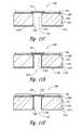
- FIGS. 12A-12Care schematic side cross-sectional views illustrating stages of a method for depositing an electrically conductive fill material into a blind hole in accordance with another embodiment of the invention.
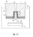
- FIG. 13is a schematic side cross-sectional view illustrating a stage of a method for depositing an electrically conductive fill material into a blind hole in accordance with yet another embodiment of the invention.
- FIG. 14is a schematic side cross-sectional view illustrating a stage of a method for depositing an electrically conductive fill material into a blind hole in accordance with still another embodiment of the invention.
- FIG. 15is a schematic side cross-sectional view of a packaged microelectronic device in accordance with one embodiment of the invention.
- the following disclosuredescribes several embodiments of methods for forming electrically conductive through-wafer interconnects in microelectronic workpieces and microelectronic workpieces having such interconnects.
- Such interconnectselectrically couple terminals or other conductive elements proximate to one side of the workpiece to conductive elements proximate to the other side of the workpiece.
- the followingdescribes several embodiments of methods for forming interconnects in (1) through-holes extending through the workpiece, and (2) blind holes or vias extending to an intermediate depth in the workpiece.
- One aspect of the inventionis directed toward a method for manufacturing a microelectronic workpiece having a plurality of microelectronic dies.
- the individual diesinclude an integrated circuit and a terminal electrically coupled to the integrated circuit.
- the methodincludes forming an opening in the workpiece in alignment with the terminal.
- the openingcan be a through-hole extending through the workpiece or a blind hole that extends only partially through the substrate.
- the openingcan be etched and/or cut using a laser.
- the methodcontinues by applying an isolation material to at least a portion of the opening. The isolation material electrically insulates the other components in the substrate from the solder material filling the opening.
- the methodfurther includes depositing a solder material into at least a portion of the opening and in electrical contact with the terminal to construct an electrically conductive interconnect in the workpiece.
- the workpiececan be thinned either before or after forming the hole.
- One embodiment of a method for constructing the interconnectincludes depositing an isolation material onto the workpiece and into the opening using a pulsed layer deposition process. The method continues by depositing a barrier layer onto the workpiece and into the opening. The barrier layer protects the other components in the workpiece from the other materials in the opening (e.g., copper). The method then includes depositing a seed layer onto the workpiece and into the opening. A layer of resist is then deposited over the workpiece and an aperture is formed over the opening. A conductive layer is then deposited into the opening and over at least a portion of the seed layer to form a conductive liner in the opening. The conductive layer can act as a wetting agent for filling the opening with solder material to form the interconnect. The opening is then filled with the solder material. The layer of resist is then stripped from the workpiece and the exposed portions of the seed layer are removed using a suitable etching process.
- constructing the interconnectincludes depositing an isolation material including a silane-based oxide material onto the workpiece and into the opening. The method then includes depositing a barrier layer onto the workpiece and into the opening. The method further includes depositing a wetting layer over at least a portion of the barrier layer. The opening is then filled with the solder material.
- constructing the interconnectcan include depositing a dielectric liner onto the workpiece and into the opening.
- the dielectric linercan include a furnace oxide or another suitable dielectric material.
- the methodfurther includes depositing a conductive layer over at least a portion of the dielectric liner and depositing a wetting layer over at least a portion of the conductive layer. The opening is then filled with the solder material.
- a microelectronic assemblyincluding a microelectronic workpiece having a substrate with a front side and a backside.
- the assemblycan also include a plurality of microelectronic dies on and/or in the substrate.
- the individual diesinclude an integrated circuit and a terminal electrically coupled to the integrated circuit.
- the assemblycan also include an opening extending at least partially through the substrate and in alignment with the terminal.
- An isolation materialcan be disposed in the opening an in contact with the substrate.
- the isolation materialincludes a low temperature oxide applied using a pulsed layer deposition process.
- the isolation materialcan include a silane-based oxide material or another suitable dielectric material.
- the assemblyfurther includes an electrically conductive interconnect in at least a portion of the opening and in electrical contact with the terminal.
- the interconnectincludes a solder material, such as a SnAgCu solder, a SnPb solder, a AuSn solder, a solder having another composition, and/or other suitable materials or alloys of materials having the desired conductivity. Solder balls or other external electrical contacts are subsequently attached to the interconnects at the backside of the workpiece.
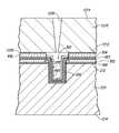
- FIG. 2is a side cross-sectional view of a microelectronic workpiece 200 configured in accordance with several embodiments of the invention.
- the microelectronic workpiece 200 illustrated in FIG. 2includes a substrate 210 having a front side 212 , a backside 214 , and a plurality of microelectronic dies 220 formed on and/or in the substrate 210 .
- the individual dies 220can include an integrated circuit 222 and external contacts 230 electrically coupled to the integrated circuit 222 .
- the external contacts 230 shown in FIG. 2provide a small array of ball-pads within the footprint of each die 220 .
- Each external contact 230can include a terminal 232 (e.g., a bond-pad), an external contact pad 234 (e.g., a ball-pad), and an interconnect 236 coupling the terminal 232 to the contact pad 234 .
- the terminals 232are on the front side 212 of the substrate 210
- the contact pads 234are on the backside 214 of the substrate 210
- the interconnects 236are through-wafer interconnects that extend completely through the substrate 210 to couple the terminals 232 to the contact pads 234 .
- the dies 220may not include the terminals 232 on the front side 212 of the substrate 210 such that the integrated circuit 222 is coupled directly to the contact pads 234 on the backside 214 of the substrate 210 by interconnects that extend only through a portion of the substrate 210 .
- the microelectronic workpiece 200can be cut along lines A-A to singulate the microelectronic dies 220 .
- the interconnects 236enable the contact pads 234 to be on the backside 214 of the substrate 210 , which provides several advantages. More specifically, the external contact pads 234 can be located on the backside 214 of the substrate 210 because the interconnects 236 shown in FIG. 2 are through-wafer interconnects that extend to the backside 214 of the substrate 210 .
- the backside arrays of contact pads 234allow the dies 220 to be stacked on other dies or attached directly to an interposer substrate without peripheral wirebonds.
- the dies 220 with the interconnects 236are more robust than dies that require wire-bonds, and the individual dies 220 also have a significantly smaller footprint and profile than the conventional stacked devices shown in FIG. 1 . Accordingly, the dies 220 can be used in smaller electronic devices.
- FIG. 3is a flow chart of a method 300 for forming interconnects in a microelectronic workpiece in accordance with several embodiments of the invention.
- the method 300includes forming a hole or deep via through the workpiece at stage 310 .
- the hole or viacan be created before, during, or after all the other microelectronic components of the workpiece are fabricated.
- the method 300includes forming a dielectric liner in the hole or via.
- the dielectric linerelectrically insulates the components of the workpiece from conductive material that is subsequently deposited into the hole or via to form an interconnect.
- the dielectric linercan include a variety of materials and/or layers.
- a wetting layeris formed on the dielectric liner.
- the wetting layerfacilitates depositing subsequent materials into the hole or via.
- the wetting layercan also include a variety of materials and/or layers.
- the hole or viais filled with solder at stage 340 to form an electrically conductive interconnect through at least a portion of the workpiece.
- the soldercan be deposited into the hole or via in a number of ways.
- the workpiecemay be thinned at an optional stage 350 either before stage 310 or after stage 340 . If the workpiece is thinned after stage 340 , for example, the thinning process will generally expose a portion of the interconnect at a backside of the workpiece.
- the dielectric liner of stage 320is formed using a pulsed layer deposition process.
- a barrier layer of tungstenis then applied over at least a portion of the dielectric liner.
- a layer of nickelis deposited onto the tungsten using an electroless plating process.
- the hole or viais filled with a SnAgCu solder using a vacuum reflow process.
- a dielectric lineris formed using a silane-based oxide material at stage 320 .
- a barrier layer of tungstenis then deposited over at least a portion of the dielectric liner.
- a layer of nickelis applied over the tungsten using an electroless plating process.
- the hole or viais filled at stage 340 with a SnPb solder.
- a dielectric lineris formed using a furnace oxide at stage 320 .
- a layer of TiCI 4 TiNis formed on at least a portion of the furnace oxide and a layer of nickel is deposited onto the layer of TiCI 4 TiN using an electroplating process.
- the hole or viais filled with a SnPb solder applied using a solder wave process.
- FIGS. 4-14Various embodiments of the individual steps of the method 300 for forming interconnects set forth above with respect to FIG. 3 are described in detail below with reference to FIGS. 4-14 ; accordingly, like reference numbers refer to like components in FIGS. 4-14 . More specifically, various embodiments of methods for forming interconnects in through-holes are described in more detail below under heading D entitled “Methods for Forming Interconnects in Through-Holes,” embodiments of methods for forming interconnects in blind holes are described in greater detail under heading E entitled “Methods for Forming Interconnects in Blind Holes,” and an embodiment of a microelectronic assembly is described in detail below under heading F entitled, “Embodiments of Microelectronic Devices.” Although the following description illustrates forming just one interconnect, it will be appreciated that a plurality of interconnects are constructed simultaneously through a plurality of dies on a wafer. Additionally, several embodiments of specific microelectronic assemblies are described throughout these sections.
- FIGS. 4-7Billustrate several embodiments of methods for forming the interconnects 236 shown in FIG. 2 . More specifically, FIGS. 4-7B illustrate methods for forming interconnects by filling through-holes extending completely through the workpiece 200 with a solder material. Each of the embodiments described below can be used for implementing each of the examples set forth above with respect to FIG. 3 .
- FIG. 4is a flow chart of a method 400 for forming interconnects in the workpiece.
- the method 400can be generally similar to the method 300 described above, except that the method 400 is directed specifically at constructing interconnects in through-holes.
- the method 400first includes forming a through-hole in the workpiece at stage 410 .
- the through-holeis etched or cut with a laser completely through the workpiece. If a laser is used, then at stage 415 the through-hole will be cleaned to remove the ablated byproducts (i.e., slag) and/or other undesirable byproducts resulting from the laser.
- the method 400includes forming a dielectric liner in the through-hole.
- one or more conductive layerscan be deposited onto the dielectric liner at optional stage 425 .
- a wetting agentis applied to the dielectric liner (or the optional conductive layer) at stage 430 .
- the method 400can include a spacer etch at optional stage 435 to remove material (e.g., the dielectric liner and/or wetting agent) from surfaces that are transverse (i.e., not parallel) relative to the direction of the etchant.
- the method 400includes depositing solder into the through-hole to form an interconnect. Finally, the end of the interconnect is capped at stage 450 to electrically couple the interconnect to the corresponding terminal.
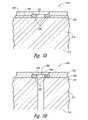
- FIGS. 5A-5Gare schematic side cross-sectional views illustrating one embodiment of method 400 ( FIG. 4 ) in greater detail.
- FIG. 5Ais a schematic side cross-sectional view of the area for one of the external contacts 230 shown in FIG. 2 .
- a first dielectric layer 550is applied to the front side 212 of the substrate, and a second dielectric layer 552 is applied over the first dielectric layer 550 .
- the second dielectric layer 552is patterned and etched to expose the terminal 232 . After exposing the terminal 232 , a first hole 554 is formed through the terminal 232 .
- the first hole 554can be formed by etching the center of the terminal 232 , but in other embodiments the first hole 554 can be formed using other suitable methods (e.g., laser).
- the dielectric layers 550 and 552can be a polyimide material, but these dielectric layers can also be other nonconductive materials in other embodiments.
- the first dielectric layer 550 and/or one or more of the subsequent dielectric layerscan be a low temperature chemical vapor deposition (low temperature CVD) material, such as tetraethylorthosilicate (TEOS), parylene, silicon nitride (Si 3 N 4 ), silicon oxide (SiO 2 ), and/or other suitable materials.
- TEOStetraethylorthosilicate
- parylenesilicon nitride
- SiO 2silicon oxide
- the foregoing list of dielectric materialsis not exhaustive.
- the dielectric layers 550 and 552are not generally composed of the same material. In addition, one or both of these layers
- a passage or through-hole 560is then cut through the substrate 210 .
- the through-hole 560extends through the substrate 210 to the first hole 554 in the terminal 232 .
- the through-hole 560 and the first hole 554together form a passage 562 extending through the die 220 .
- the through-hole 560can be formed by etching through the material using one or more etches.
- the through-hole 560can alternatively be formed using a laser, as described below in FIG. 6B , in addition to or in lieu of etching.
- etching the through-hole 560may be easier because the slag does not need to be cleaned from the through-hole 560 .
- Another advantage of etching the through-hole 560is that the through-hole 560 has rounded corners, which reduce stress points within the hole so that an interconnect constructed within the hole is less susceptible to stress damage.
- a further advantage of using an etching processis that the front side 212 of the substrate 210 can be patterned and etched to simultaneously form a plurality of through-holes 560 aligned with corresponding terminals 232 .
- a third dielectric layer 570is applied to the die 220 to line the sidewall of the through-hole 560 in the substrate 210 .
- the third dielectric layer 570is an isolation material that electrically insulates the components of the substrate 210 from an interconnect that is subsequently formed in the passage 562 as described in greater detail below.
- the third dielectric layer 570not only lines the exposed portions of the substrate 210 in the through-hole 560 , but it also covers the terminal 232 and the second dielectric layer 552 .
- the third dielectric layer 570can be a low temperature CVD oxide.
- the third dielectric layer 570is an aluminum-rich oxide material applied using a pulsed layer deposition process.
- the third dielectric layer 570includes a silane-based oxide material. In still further embodiments, the third dielectric layer 570 can include other suitable dielectric materials.
- a barrier layer 571is then deposited onto the substrate 210 over the third dielectric layer 570 .
- the barrier layer 571can be deposited onto the substrate 210 using a vapor deposition process, such as CVD or physical vapor deposition (PVD).
- the barrier layer 571can be composed of W, Ta, or other suitable materials.
- a first conductive layer 572is deposited onto the die 220 .
- the first conductive layer 572covers the barrier layer 571 .
- the first conductive layer 572is generally a wetting agent to facilitate depositing a conductive fill material into the passage 562 .
- the first conductive layer 572is nickel (Ni).
- the first conductive layer 572may be another suitable material and/or the passage 562 can be coated with one or more additional layers. For example, additional layers may be added to the third dielectric layer 570 before application of the first conductive layer 572 .
- a seed layer and/or additional conductive layerscan be deposited onto the barrier layer 571 before the application of the first conductive layer 572 . Suitable materials and methods for applying the seed layer and additional conductive layer are described below with respect to FIGS. 9D and 9E .
- the first conductive layer 572is etched to leave a portion of the first conductive layer 572 lining the passage 562 .
- the first conductive layer 572can be etched using a “dry etch” or “spacer etch” that preferentially removes material from surfaces that are transverse (i.e., not parallel) relative to the direction of the etchant.
- the vertical portions of the first conductive layer 572remain on the barrier layer 571 and the third dielectric layer 570 in the passage 562 .
- a conductive fill material 580is deposited into the passage 562 to form an interconnect 582 extending through the die 220 .
- the fill material 580is SnAgCu solder deposited into the passage 562 using a vacuum reflow process.
- the fill material 580can be SnPb solder or solder materials having other compositions.
- the fill material 580may be deposited into the passage 562 using other methods, such as solder wave solder, plating solder, screen printing a solder plate, placing a pre-formed sphere of solder in the passage 562 and melting the sphere, injecting a solder paste or molten solder into the passage 562 , or other suitable methods known to those of skill in the art.
- a cap 584is formed at one end of the interconnect 582 to electrically couple the interconnect 582 to the terminal 232 .
- the cap 584is Ni that is plated onto the interconnect 582 .
- the cap 584can be omitted by overfilling the passage 562 with the fill material 580 such that the fill material itself forms a connection to the terminal 232 .
- a solder ball 586 or other external interconnect structurecan be attached to the interconnect 582 at the backside 214 of the substrate 210 to provide an external connection to other electronic devices on the backside of the die 220 .
- the passage 562extends through the entire die 220 .
- the passage 562is accordingly easier to clean and fill than would otherwise be the case in certain situations when the passage is “blind” (i.e., a passage that extends only partially through the workpiece).
- solderis relatively inexpensive, and machinery and processes for working with solder are well known in the semiconductor arts. Furthermore, solder can be deposited into the passage 562 at fairly low temperatures, which is advantageous because high temperatures can damage the various microelectronic components on and/or in the workpiece.
- FIGS. 6A-6Fare schematic side cross-sectional views illustrating a method for forming a through-wafer interconnect in accordance with another embodiment of method 400 ( FIG. 4 ).
- the first part of this methodis similar to the steps described above with reference to FIG. 5A .
- the method shown in FIG. 6Adiffers from that described above in FIG. 5A in that a third dielectric layer 656 is deposited onto the die 220 to cover the terminal 232 and fill the first hole 554 before cutting a through-hole through the substrate 210 .
- a second hole 658is etched through the third dielectric layer 656 to expose the terminal 232 .
- the second hole 658is typically etched to the front side 212 of the substrate 210 to open the first hole 554 .
- a passage or through-hole 660is then cut through the first substrate 210 .
- the through-hole 660extends through the substrate 210 to the first hole 554 in the terminal 232 .
- the through-hole 660 and the first hole 554together form a passage 662 extending through the die 220 .
- the through-hole 660can be formed using a laser (shown schematically) to cut through the substrate 210 from the backside 214 toward the front side 212 .
- the lasercan conceivably cut from the front side 212 toward the backside 214 .
- the lasercan be aligned with respect to the terminal 232 using scanning/alignment systems known in the art.
- the through-hole 660After forming the through-hole 660 , it is cleaned to remove ablated byproducts (i.e., slag) and/or other undesirable byproducts resulting from the laser. Suitable chemical cleaning agents and processes are disclosed in U.S. patent application Ser. No. 10/879,398, which was previously incorporated by reference. The slag in the through-hole 660 , however, may not be cleaned in some embodiments of this method.
- a fourth dielectric layer 670is applied to the die 220 to line the sidewall of the through-hole 660 in the substrate 210 .
- the fourth dielectric layer 670can be applied using CVD, PVD, atomic layer deposition (ALD), or other deposition processes.
- the fourth dielectric layer 670not only lines the exposed portions of the substrate 210 in the through-hole 660 , but it also covers the terminal 232 and the third dielectric layer 656 .
- the fourth dielectric layer 670can be a low temperature CVD oxide, but in other embodiments the fourth dielectric layer 670 can be other suitable dielectric materials.
- the fourth dielectric layer 670electrically insulates the components of the substrate 210 from an interconnect that is subsequently formed in the passage 662 as described in greater detail below.
- a first conductive layer 672is deposited onto the die 220 .
- the first conductive layer 672covers the fourth dielectric layer 670 .
- the first conductive layer 672is generally composed of a metal, such as TiN, but in other embodiments the first conductive layer 672 can be composed of other suitable materials known to those of skill in the art. As explained below, the first conductive layer 672 provides a seed layer for plating another layer of metal into the passage 662 .
- the first conductive layer 672is etched from the horizontal and diagonal surfaces of the die 220 using a spacer etch or other process as described above with respect to FIG. 5E .
- the front side of the fourth dielectric layer 670is then etched to remove the fourth dielectric layer 670 from the horizontal and diagonal surfaces of the front side 212 of the die 220 , and then the third dielectric layer 656 ( FIG. 6C ) is removed from the die 220 .
- the fourth dielectric layer 670remains under the first conductive layer 672 in the passage 662 and on the backside 214 of the substrate 210 in this embodiment.
- the fourth dielectric layer 670can be etched using a dry etch or spacer etch as described above.
- the third dielectric layer 656can be removed using a suitable isotropic or anisotropic etch, a washing process, or a chemical mechanical planarization (CMP) process depending on the composition of the third dielectric layer 656 .
- CMPchemical mechanical planarization
- a second conductive layer 674is deposited onto the remaining portions of the first conductive layer 672 in the passage 662 .
- the second conductive layer 674is generally a wetting agent to facilitate depositing metals into the passage 662 .
- the second conductive layer 674is Ni and the first conductive layer 672 is TiN so that the Ni can be plated onto the TiN using a suitable electroless plating process.
- the passage 662can be coated with other suitable materials using other methods, or one or more of the first and second conductive layers 672 and 674 may be omitted.
- a conductive fill material 680is deposited into the passage 662 to form an interconnect 682 extending through the die 220 .
- the fill material 680can include a SnPb solder deposited into the passage 662 using a solder wave process.
- the fill material 680may be a solder material having a different composition or another suitable electrically conductive material. Further, the fill material 680 may be deposited into the passage 662 using other methods.
- FIGS. 7A and 7Billustrate another method for forming an interconnect in accordance with yet another embodiment of the invention.
- the first part of this methodis similar to the steps described above with reference to FIG. 5A , but a hole is not etched in the terminal 232 .
- a through-hole 760is formed through both the substrate 210 and the terminal 232 .
- the through-hole 760can be formed using a laser (shown schematically), etching, or another suitable process.
- a first type of slagi.e., silicon
- a second type of slagi.e., metal
- the cleaning agents used to clean the through-hole 760may be limited to chemistries that do not attack or otherwise degrade either the terminal 232 or the substrate 210 .
- the die 220can undergo additional steps that are at least generally similar to those described above with reference to FIGS. 5C-5G or FIGS. 6C-6F to construct a through-wafer interconnect.
- the embodiments described above with reference to FIGS. 5A-7Binclude three methods for forming and/or filling through-holes in microelectronic workpieces that extend through bond-pads and/or associated substrates. In other embodiments, other methods can be used to form and/or fill such through-holes. Accordingly, the present invention is not limited to the particular methods for forming and/or filling the through-holes described above, but it also includes alternative methods for providing an electrically conductive material in a through-hole to form an array of ball-pads on the backside of the die.
- FIGS. 8-14illustrate additional methods for constructing the interconnects 236 shown in FIG. 2 .
- the methods shown in FIG. 8-14are related to those shown above in FIGS. 4-7B , but form an interconnect in a blind hole or via in the substrate 210 instead of a through-hole extending through the substrate.
- Each of the embodiments described belowcan be used for implementing each of the examples set forth above with respect to FIG. 3 .
- FIG. 8is a flow chart of a method 800 for forming interconnects in blind holes in a microelectronic workpiece.
- the method 800can be generally similar to the method 300 described above with respect to FIG. 3 , except that the method 800 is directed specifically at constructing interconnects in blind holes or vias.
- the method 800first includes forming a blind hole or blind via that does not extend completely through the workpiece at stage 810 .
- the blind holecan be etched or cut with a laser. If a laser is used, then at stage 815 the blind hole is cleaned to remove the slag and/or other undesirable byproducts resulting from the laser.
- the method 800includes forming a dielectric liner in the blind hole.
- a conductive layeris then deposited onto the dielectric liner at stage 830 , and a wetting agent is applied to the dielectric liner at stage 840 .
- a first optional stage 842includes a spacer etch to remove material (e.g., the dielectric liner, conductive layer, and/or wetting agent) from non-vertical surfaces.
- a second optional stage 844includes forming a vent hole in fluid communication with the blind hole.
- the vent holewhich can be formed in the workpiece or a support member attached to the workpiece, extends to the blind hole to vent fluids or other gases that could otherwise be trapped in the blind hole.
- the method 800continues at stage 850 by depositing solder into the blind hole to form an interconnect.
- a third optional stage 855includes thinning the workpiece.
- the optional thinning stage 855can occur before forming the blind holes in stage 810 or after filling the blind holes with the conductive material in stage 850 .
- an end of the interconnectis capped at stage 860 to electrically couple the interconnect to the corresponding terminal.
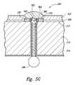
- FIGS. 9A-9Jare schematic side cross-sectional views illustrating one embodiment of method 800 in greater detail.
- FIG. 9Ais a schematic side cross-sectional view of the area for one of the external contacts 230 shown in FIG. 2 .
- the first dielectric layer 550is applied to the front side 212 of the substrate, and the second dielectric layer 552 is applied over the first dielectric layer 550 .
- the second dielectric layer 552is patterned and etched to expose the terminal 232 .
- a mask 910is applied over the second dielectric layer 552 and patterned.
- the mask 910can be a layer of resist that is patterned according to the arrangement of terminals 232 on the substrate 210 . As such, the mask 910 has an opening 912 over the terminal 232 .
- a hole or aperture 920is formed through at least part of the substrate 210 .
- the hole 920extends through the terminal 232 , the first dielectric layer 550 , and a portion of the substrate 210 to define a blind hole or via 925 .
- a “blind hole”refers to a hole or aperture that extends only partially through the substrate 210 or is otherwise closed at one end.
- the hole 920is formed by etching through the materials using one or more individual etches. After forming the hole 920 , the mask 910 is removed from the die 220 .
- the hole 920can alternatively be formed using a laser in addition to or in lieu of etching. If a laser is used to form all or a portion of the hole 920 , it is typically cleaned using chemical cleaning agents to remove slag or other contaminants as described above with respect to FIG. 6B . Although laser cutting the hole 920 may be advantageous because the substrate 210 does not need to be patterned, etching the hole 920 may be easier because the slag does not need to be cleaned from the hole 920 . Etching the hole 920 may also include many of the additional advantages described above with respect to etching through-holes in FIG. 5B .
- a third dielectric layer 930is deposited onto the substrate 210 to line the sidewalls of the blind hole 925 within the substrate 210 .
- the third dielectric layer 930electrically insulates components in the substrate 210 from an interconnect that is subsequently formed in the blind hole 925 , as described in greater detail below.
- the third dielectric layer 930can be a low temperature CVD oxide applied using a pulsed layer deposition process similar to that described above with respect to FIG. 5C .
- the third dielectric layer 930can be a silane-based oxide material or other suitable dielectric materials.
- a barrier layer 932is then deposited onto the substrate 210 over the third dielectric layer 930 .
- the barrier layer 932generally covers the second dielectric layer 552 and the terminal 232 in addition to the third dielectric layer 930 .
- the barrier layer 932can be deposited onto the substrate 210 using a vapor deposition process, such as CVD or PVD.
- the barrier layer 932can be composed of W, Ta, or other suitable materials.
- a seed layer 934is deposited onto the barrier layer 932 .
- the seed layer 934can be deposited using vapor deposition techniques, such as CVD, PVD, and/or ALD.
- the seed layer 934can be composed of Cu or other suitable materials.
- the thickness of the seed layer 934is generally 400 to 2000 Angstroms.
- the seed layer 934may not cover the barrier layer 932 uniformly. This may cause subsequent electroplating processes to not apply a uniform metal layer onto the workpiece. If the seed layer 934 is deficient, it can be enhanced using an enhancement process that fills voids or noncontinuous regions of the seed layer 934 to form a more uniform seed layer.
- One suitable seed layer enhancement processis described in U.S. Pat. No. 6,197,181, which is incorporated by reference.
- a resist layer 936is deposited onto the seed layer 934 , and the resist layer 936 is patterned to have an opening 937 over the terminal 232 and corresponding blind hole 925 .
- a first conductive layer 938can then be deposited onto the exposed portions of the seed layer 934 in the blind hole 925 .
- the first conductive layer 938can be Cu that is deposited onto the seed layer 934 in an electroless plating operation, electroplating operation, or another suitable method.
- the application of the first conductive layer 938is an optional step that can be omitted in several embodiments.
- a second conductive layer 940is deposited onto the first conductive layer 938 in the blind hole 925 .
- the second conductive layer 940is a wetting agent that facilitates depositing subsequent materials into the blind hole 925 .
- the second conductive layer 940can be Ni that is deposited onto the first conductive layer 938 using an electroless plating process.
- the blind hole 925may be coated with other suitable materials using other methods.
- a vent hole 950is formed in the substrate 210 extending from a bottom portion of the blind hole 925 to the backside 214 of the substrate 210 .
- the vent hole 950can be formed using a laser to cut through the substrate 210 from the backside 214 to the bottom of the blind hole 925 .
- the lasercan be aligned with the blind hole 925 and/or corresponding terminal 232 using scanning/alignment systems known in the art.
- a suitable laseris the Xise200 commercially available from Xsil Ltd. of Dublin, Ireland.
- vent hole 950can be cleaned using suitable cleaning agents described above with respect to FIG. 6B .
- the vent hole 950can be formed using an etching process or another suitable method.
- the vent hole 950may not be formed in the substrate 210 and/or the vent hole 950 may be formed at a different stage of the method.
- a conductive fill material 960is deposited into the blind hole 925 to form an interconnect 962 .
- the interconnect 962has a first end 963 proximate to the terminal 232 and a second end 964 at the bottom of the blind hole 925 .
- the fill material 960is SnAgCu solder.
- the fill material 960can be SnPb solder, solder materials having other compositions, or another suitable material.
- the fill material 960can be deposited into the blind hole 925 using plating processes, solder wave processes, screen printing processes, reflow processes, vapor deposition processes, or other suitable techniques.
- the plating processesfor example, can include electroless and/or electroplating processes.
- the resist layer 936is removed from the substrate 210 and a suitable etching process is used to remove the remaining portions of the seed layer 934 and barrier layer 932 on the front side 212 of the substrate 210 .
- the substrate 210is thinned to a desired thickness “T” by removing material from the backside 214 of the substrate 210 .
- the second end 964 of the interconnect 962is exposed after removing material from the backside 214 .
- the initial thickness of the substrate 210is approximately 750 ⁇ m, and the final thickness T is approximately 100-500 ⁇ m. The initial and final thicknesses can be different in other embodiments.
- the backside 214 of the substrate 210can be thinned using CMP processes, dry etching processes, chemical etching processes, chemical polishing, grinding procedures, or other suitable processes.
- the substrate 210can be recessed to bring out a solder “post” (not shown) after thinning the workpiece.
- the solder postis positioned to allow connection of the interconnect to solder balls, external devices, and/or boards.
- vent hole 950allows trapped air, gases, or volatile solvents to escape from the larger blind hole 925 when filling the blind hole with the fill material 960 .
- the vent hole 950allows the fill material 960 to more easily flow into the blind hole 925 and mitigates the likelihood of voids or discontinuities in the interconnect 962 .
- vent hole 950will not become plugged while depositing the fill material 960 into the blind hole 925 . Because the vent hole 950 is formed after depositing the second conductive layer 940 , the fill material 960 deposited into the blind hole 925 will only flow as far as the wetting material (e.g., the second conductive layer 940 ) and will not flow into the vent hole 950 . Accordingly, the vent hole 950 will remain open during the filling process and allow any gases and/or fluids trapped in the blind hole 925 to escape.
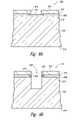
- FIGS. 10A-10Eillustrate a method for forming a through-wafer interconnect for the die 220 in accordance with another embodiment of the invention.
- FIG. 10Ashows the die 220 at a point in the process that is similar to the die 220 illustrated in FIG. 9B .
- the method shown in FIGS. 10A-10Ediffers from that described above with reference to FIGS. 9A-9J in that the layers of material deposited into the blind hole 925 are different materials and a vent hole is not formed in the substrate 210 . Therefore, referring to FIG. 10A , the hole or aperture 920 is formed through at least part of the substrate 210 .
- the hole 920extends through the terminal 232 , the first dielectric layer 550 , and a portion of the substrate 210 defining a blind hole 925 .
- the hole 920is formed by etching through the materials using one or more individual etches or a laser as described above with respect to FIG. 9B .
- a third dielectric layer 1030is deposited onto the die 220 to line the sidewall of the blind hole 925 within the substrate 210 .
- the third dielectric layer 1030generally covers the second dielectric layer 552 and the terminal 232 in addition to lining the sidewalls of the blind hole 925 .
- the third dielectric layer 1030can include a furnace oxide or another suitable dielectric material described above.
- a first conductive layer 1040is then deposited onto the third dielectric layer 1030 .
- the first conductive layer 1040can be composed of TiN or other suitable materials.
- the first conductive layer 1040 and the third dielectric layer 1030are etched from the horizontal and diagonal surfaces of the die 220 using one or more spacer etches. This leaves a portion of the third dielectric layer 1030 lining the sidewall of the blind hole 925 and a portion of the first conductive layer 1040 on the third dielectric layer 1030 .
- the first conductive layer 1040is etched first using a first spacer etch that does not etch the third dielectric layer 1030 , and then the third dielectric layer 1030 is etched using a second spacer etch that does not etch the first conductive layer 1040 in the blind hole 925 .
- a second conductive layer 1042is then deposited onto the first conductive layer 1040 and the blind hole 925 is filled with a conductive material.
- the second conductive layer 1042can be a wetting agent to facilitate filling the blind hole 925 with the conductive fill material.
- the second conductive layer 1042can accordingly be Ni or another suitable material deposited onto the remaining portions of the first conductive layer 1040 using an electroless plating process.
- a conductive fill materialis then deposited into the blind hole 925 to form an interconnect 1050 in the die 220 .
- the fill materialcan include a SnPb solder deposited into the blind hole 925 using a solder wave process.
- the fill materialmay be a solder material having a different composition or another suitable electrically conductive material.
- the fill materialmay be deposited into the blind hole 925 using other methods, such as plating processes, vapor deposition processes, or other suitable methods.
- the interconnect 1050has a first end 1052 proximate to the terminal 232 and a second end 1054 at the bottom of the blind hole 925 .
- the backside 214 of the substrate 210is then thinned using a CMP process or another suitable grinding process.
- the backside 214 of the substrate 210is ground to a desired thickness “T” until the second end 1054 of the interconnect 1050 is exposed.
- the substrate thickness Tcan be approximately 200-1,000 ⁇ m, 300-750 ⁇ m, or about 500 ⁇ m.
- a fourth dielectric layer 1060is applied to the backside 214 of the substrate 210 and then etched to expose the second end 1054 of the interconnect 1050 , and a cap 1070 is formed on the first end 1052 of the interconnect 1050 to electrically couple the terminal 232 to the interconnect 1050 .
- FIGS. 11A-11Hillustrate a method for forming an interconnect in a blind hole in accordance with yet another embodiment of the invention.
- This methodbegins with the substrate 210 , the first dielectric layer 550 , the second dielectric layer 552 , and the terminal 232 as shown in FIG. 9A .
- a portion of the second dielectric layer 552is removed to expose the terminal 232 .
- the process shown in FIGS. 11A-11Hdiffers from the methods shown in FIGS. 9A-9J and FIGS. 10A-10E in that a hole or aperture is formed from the backside 214 of the substrate 210 instead of the front side 212 .
- the substrate 210can be thinned by grinding the backside of the substrate 210 to form the backside 214 to a desired thickness “T.”
- the substrate thickness Tcan be approximately 200-1,000 ⁇ m, 300-750 ⁇ m, or about 500 ⁇ m.
- the backside 214 of the substrate 210can be thinned using CMP processes, dry grinding processes, or other suitable grinding procedures.
- a third dielectric layer 1110is applied over the backside 214 of the substrate 210 .
- the third dielectric layer 1110can be a polyimide material or another nonconductive material generally similar to the first and second dielectric layers 550 and 552 described above with respect to FIG. 5A . In alternate embodiments, one or more of the dielectric layers 550 / 552 / 1110 may be omitted.
- FIGS. 11B-11Hillustrate subsequent stages of forming this embodiment of the interconnect.
- FIG. 11Bis a schematic side cross-sectional view of the die 220 after a hole or aperture 1120 has been formed through the substrate 210 in alignment with a corresponding terminal 232 .
- the hole 1120is formed by patterning the backside 214 of the substrate 210 and etching through the substrate 210 from the backside 214 .
- the hole 1120can be etched using a process that selectively removes material from the substrate 210 compared to the first dielectric layer 550 .
- the first dielectric layer 550can accordingly be an etch-stop.
- the first dielectric layer 550 directly beneath the terminal 232is etched to expose a backside 1122 of the terminal 232 .
- the hole 1120 and the exposed backside 1122 of the terminal 232define a blind hole 1125 .
- the second etching process for the first dielectric layer 550can be different than the first etching process for the substrate 210 .
- the second etching processcan selectively remove material from the first dielectric layer 550 at a higher etch rate than from either the substrate 210 or the terminal 232 .
- the second etching processaccordingly does not alter the general structure of the terminal 232 and/or the substrate 210 .
- the substrate 210 and the first dielectric layer 550can be etched using a single etch to form the hole 1120 .
- the hole 1120can alternatively be formed using a laser in addition to or in lieu of etching. If a laser is used to form all or a portion of the hole 1120 , it is typically cleaned using chemical cleaning agents to remove slag or other contaminants as described previously.
- a fourth dielectric layer 1130is applied to the die 220 to line the sidewall of the blind hole 1125 .
- the fourth dielectric layer 1130also covers the backside 1122 of the terminal 232 and the third dielectric layer 1110 .
- the fourth dielectric layer 1130can be a low temperature CVD oxide or another suitable dielectric material.
- the fourth dielectric layer 1130is etched from the horizontal and diagonal surfaces of the die 220 using a spacer etch or dry etch. This leaves portions of the fourth dielectric layer 1130 lining the sidewall of the blind hole 1125 to electrically insulate components in the substrate 210 from conductive materials subsequently deposited into the blind hole 1125 .
- a first conductive layer 1140is deposited onto the die 220 and then etched to cover the portion of the fourth dielectric layer 1130 lining the sidewall of the blind hole 1125 .
- the first conductive layer 1140is deposited over the backside 214 of the die 220 so that it covers the third dielectric layer 1110 , the fourth dielectric layer 1130 , and the backside 1122 of the terminal 232 .
- the first conductive layer 1140is generally composed of a metal, such as TiN, but in other embodiments the first conductive layer 1140 can be composed of other suitable materials.
- the first conductive layer 1140is then etched from the horizontal and diagonal surfaces of the die 220 using a spacer etch to leave the remaining portions of the first conductive layer 1140 on the fourth dielectric layer 1130 in the blind hole 1125 .
- a second conductive layer 1142is deposited onto the remaining portions of the first conductive layer 1140 in the blind hole 1125 .
- the second conductive layer 1142is a wetting agent that facilitates depositing subsequent metals into the blind hole 1125 .
- the second conductive layer 1142can be Ni that is deposited onto a first conductive layer 1140 composed of TiN in an electroless plating operation.
- the blind hole 1125can be coated with other suitable materials using other methods, or one or more of the first and second conductive layers 1140 and 1142 may be omitted.
- a conductive fill material 1150is deposited into the blind hole 1125 to form an interconnect 1152 extending through the die 220 .
- the fill material 1150can include a SnPb solder deposited into the blind hole 1125 using a solder wave process.
- the fill material 1150may be a solder material having a different composition or another suitable electrically conductive material.
- the fill material 1150may be deposited into the blind hole 1125 using electroplating, electroless plating, or other suitable methods.
- the interconnect 1152has a first end 1153 contacting the backside 1122 of the terminal 232 and a second end 1154 at the backside 214 of the substrate 210 .
- a cap 1156can be formed at the second end 1154 of the interconnect 1152 after depositing the fill material 1150 .
- the cap 1156can be Ni electroplated onto the interconnect 1152 .
- the cap 1156can be a wetting agent and/or other material.
- a solder ball(not shown) can then be attached to the interconnect 1152 at the backside 214 of the substrate 210 to provide an external connection to other electronic devices on the backside of the die 220 .
- FIGS. 12A-14illustrate several embodiments of methods for depositing conductive fill material into the blind hole 925 . These methods are related to the methods described above with respect to FIGS. 9A-11H , and many reference numbers in FIGS. 12A-14 refer back to those in FIGS. 9A-11H .
- the method shown in FIGS. 12A-12Ccan include several steps that are at least generally similar to those described above with respect to FIGS. 9A-9H . The subsequent stages of this method differ from those described above in that a vent hole is not formed through the substrate 210 .
- the substrate 210is releasably attached to a support member 1210 (e.g., a carrier substrate) that includes a first side 1212 and a second side 1214 opposite the first side 1212 .
- the first side 1212 of the support member 1210is releasably attached to the front side 212 of the substrate 210 with an adhesive material 1220 .
- the support member 1210has a vent hole 1250 substantially aligned with the blind hole 925 .
- the vent hole 1250can be formed either before or after the support member 1210 is attached to the substrate 210 .
- the backside 214 of the substrate 210is thinned until the bottom portion of the blind hole 925 is opened.
- the substrate 210can be thinned using processes similar to those described above with respect to FIG. 9J .
- this embodimentcontinues by depositing a fill material into the blind hole 925 to form an interconnect 1264 extending through the substrate 210 .
- the fill materialcan be a solder material, such SnAgCu solder, SnPb solder, or another solder material having a different composition.
- the fill materialcan be deposited into the blind hole 925 using a solder wave process, but in other embodiments the fill material can be deposited using plating procedures or other suitable methods.
- FIG. 13illustrates a method for filling the blind hole 925 using a plating process.
- This methodcan include several steps similar to those described above with respect to FIGS. 9A-9E .
- the subsequent stages of this methodmay differ from those described above in that the fill material is plated into the blind hole 925 using a bottom-up plating process that selectively fills the blind hole 925 with fill material.
- the substrate 210can conduct electrical current to the seed layer 934 or other conductive material (e.g., conductive layers 936 and 938 ) in the blind hole 925 .
- the conductive layers 936 and 938may not be deposited onto the seed layer 934 .
- This embodimentcontinues by applying an electrical potential to the backside 214 of the substrate 210 and an electrode 1330 immersed in a plating solution 1320 .
- An electrical currentaccordingly passes through the substrate 210 such that the ions in the plating solution 1320 plate onto the seed layer 934 and progressively plate onto each other to fill the blind hole 925 and form an interconnect 1364 .
- the plating processcan be terminated when the blind hole 925 is either fully or partially filled with the fill material.
- the substrate 210can then undergo further processing as described above in FIGS. 9I and 9J .
- FIG. 14illustrates an interconnect 1410 in the die 220 in accordance with another embodiment of the invention.
- This methoddiffers from the embodiment described above with reference to FIGS. 11F-11H in that a first conductive layer and a second conductive layer are not deposited into the blind hole 1125 . Instead, a fill material is plated into the blind hole 1125 using a bottom-up plating process.
- the plating processcan be an electroless or an electrolytic process. In an electrolytic process, for example, a conductive member (not shown) is pressed against the upper side of the terminal 232 while the backside 1122 of the terminal 232 contacts a plating solution (not shown).
- a potentialis applied between the conductive member and the plating solution to plate ions in the solution onto the backside 1122 of the terminal 232 .
- the ionswill continue to plate onto each other in a bottom-up manner until the fill material fills the blind hole 1125 .
- the die 220is then removed from the plating bath and the fill material remains in the blind hole 1125 thus forming the interconnect 1410 .
- the interconnect 1410can accordingly have a backside end 1414 upon which a solder ball (not shown) can be deposited or other features can be formed.
- FIG. 15is a schematic side cross-sectional view of a microelectronic device 1500 configured in accordance with an embodiment of the invention.
- the microelectronic device 1500includes a plurality of microelectronic devices 1510 (individually identified as a first microelectronic device 1510 a and a second microelectronic device 1510 b ) interconnected in a stacked-die arrangement.
- the first and second microelectronic dies 1510 a and 1510 bcan have many components at least generally similar to the microelectronic dies 220 discussed above and illustrated in FIG. 2 .
- the first microelectronic device 1510 acan include a first microelectronic die 1520 a having an integrated circuit 1522 and external contacts 1530 electrically coupled to the integrated circuit 1522 .
- the external contacts 1530 in the illustrated embodimentinclude a terminal 1532 (e.g., a bond-pad), an external contact 1534 (e.g., a ball-pad), and an interconnect 1526 extending through the die 1520 a coupling the terminal 1532 to the contact pad 1534 .
- the interconnect 1526can be constructed using any of the methods described above with respect to FIGS. 3-14 .
- the second microelectronic device 1510 bcan include generally similar components as the first microelectronic device 1510 a.
- a plurality of solder balls 1586are coupled to corresponding contact pads 1534 at the backside of the individual devices 1510 . Accordingly, the solder balls 1586 can be used to electrically connect the first microelectronic device 1510 a to the second microelectronic device 1510 b .
- a suitable underfill material 1590 or other compoundcan also be used to structurally attach the microelectronic devices 1510 together in the illustrated stacked-die configuration.
- the solder balls 1586 at the backside of the second device 1510 bcan in turn be used to electrically connect the microelectronic device 1500 to another external device or board.
- One feature of the embodiments illustrated in FIG. 15is that the respective first and second microelectronic devices 1510 a and 1510 b are electrically connected without the need for wire-bonds.
- One advantage of this featureis that the added cost and complexity of wire-bonds is avoided.
- a further advantage of this featureis that the footprint of the microelectronic device 1500 can be reduced over conventional stacked devices having wire-bond interconnections.
Landscapes
- Engineering & Computer Science (AREA)
- Microelectronics & Electronic Packaging (AREA)
- Power Engineering (AREA)
- Physics & Mathematics (AREA)
- Condensed Matter Physics & Semiconductors (AREA)
- General Physics & Mathematics (AREA)
- Computer Hardware Design (AREA)
- Manufacturing & Machinery (AREA)
- Internal Circuitry In Semiconductor Integrated Circuit Devices (AREA)
Abstract
Description
- The present application is in a related area of subject matter as the following U.S. applications, which are incorporated herein by reference: U.S. application Ser. No. 10/879,398 entitled “Packaged Microelectronic Imagers and Methods of Packaging Microelectronic Imagers” filed Jun. 29, 2004; U.S. application Ser. No. 10/864,974 entitled “Packaged Microelectronic Imagers and Methods of Packaging Microelectronic Imagers” filed Jun. 10, 2004; and U.S. application Ser. No. ______ (Attorney Docket No. 108298799US) entitled “Microelectronic Workpieces and Methods for Forming Interconnects in Microelectronic Workpieces” filed ______.
- The present invention relates to forming interconnects in microelectronic workpieces and microelectronic workpieces formed using such methods.
- Conventional packaged microelectronic devices can include a singulated microelectronic die, an interposer substrate or lead frame attached to the die, and a molded casing around the die. The die generally includes an integrated circuit and a plurality of bond-pads coupled to the integrated circuit. The bond-pads are typically coupled to terminals on the interposer substrate or lead frame, and supply voltage, signals, etc., are transmitted to and from the integrated circuit via the bond-pads. In addition to the terminals, the interposer substrate can also include ball-pads coupled to the terminals by conductive traces supported in a dielectric material. Solder balls can be attached to the ball-pads in one-to-one correspondence to define a “ball-grid array.” Packaged microelectronic devices with ball-grid arrays are generally higher grade packages having lower profiles and higher pin counts than conventional packages using lead frames.
- Packaged microelectronic devices such as those described above are used in cellphones, pagers, personal digital assistants, computers, and many other electronic products. To meet the demand for smaller electronic products, there is a continuing drive to increase the performance of packaged microelectronic devices, while at the same time reducing the height and the surface area or “footprint” of such devices on printed circuit boards. Reducing the size of high-performance devices, however, is difficult because the sophisticated integrated circuitry of such devices requires more bond-pads, which results in larger ball-grid arrays and thus larger footprints. One technique for increasing the component density of microelectronic devices within a given footprint is to stack one device on top of another.
FIG. 1 schematically illustrates a firstmicroelectronic device 10 attached to a secondmicroelectronic device 20 in a wire-bonded, stacked-die arrangement. The firstmicroelectronic device 10 includes a die12 having an integratedcircuit 14 electrically coupled to a series of bond-pads 16. Aredistribution layer 18 electrically couples a plurality offirst solder balls 11 to corresponding bond-pads 16. The secondmicroelectronic device 20 similarly includes a die22 having an integratedcircuit 24 electrically coupled to a series of bond-pads 26. Aredistribution layer 28 electrically couples a plurality ofsecond solder balls 21 to corresponding bond-pads 26. Wire-bonds 13 extending from thefirst solder balls 11 to thesecond solder balls 21 electrically couple the firstmicroelectronic device 10 to the secondmicroelectronic device 20.- Forming the wire-
bonds 13 in the stacked device shown inFIG. 1 can be complex and/or expensive because it requires placing individual wires between corresponding pairs of contacts (e.g., thefirst solder balls 11 and the second solder balls21). Further, this type of installation may not be feasible for the high-density, fine-pitch arrays of some high-performance devices because the contacts are not spaced far enough apart to be connected to individual wire-bonds. As such, processes for packaging the dies have become a significant factor in manufacturing microelectronic devices. FIG. 1 is a side cross-sectional view of a first microelectronic device attached to a second microelectronic device in a stacked-die arrangement in accordance with the prior art.FIG. 2 is a side cross-sectional view of a microelectronic workpiece configured in accordance with several embodiments of the invention.FIG. 3 is a flow chart illustrating stages in a method for forming electrically conductive interconnects in a microelectronic workpiece in accordance with several embodiments of the invention.FIG. 4 is flow chart illustrating stages in a method for forming an electrically conductive interconnect in a through-hole in the microelectronic workpiece in accordance with an embodiment of the invention.FIGS. 5A-5G are schematic side cross-sectional views illustrating a method for forming an electrically conductive through-wafer interconnect for providing a backside array of contact pads in accordance with an embodiment of the invention.FIGS. 6A-6F are schematic side cross-sectional views illustrating a method for forming an electrically conductive through-wafer interconnect for providing a backside array of contact pads in accordance with another embodiment of the invention.FIGS. 7A and 7B are schematic side cross-sectional views illustrating a method for forming an electrically conductive through-wafer interconnect for providing a backside array of contact pads in accordance with yet another embodiment of the invention.FIG. 8 is flow chart illustrating a method for forming an electrically conductive interconnect in a blind hole in the microelectronic workpiece in accordance with an embodiment of the invention.FIGS. 9A-9J are schematic side cross-sectional views illustrating a method for forming an electrically conductive through-wafer interconnect for providing a backside array of contact pads in accordance with another embodiment of the invention.FIGS. 10A-10E are schematic side cross-sectional views illustrating a method for forming an electrically conductive through-wafer interconnect for providing a backside array of contact pads in accordance with still another embodiment of the invention.FIGS. 11A-11H are schematic side cross-sectional views illustrating a method for forming an electrically conductive through-wafer interconnect for providing a backside array of contact pads in accordance with another embodiment of the invention.FIGS. 12A-12C are schematic side cross-sectional views illustrating stages of a method for depositing an electrically conductive fill material into a blind hole in accordance with another embodiment of the invention.FIG. 13 is a schematic side cross-sectional view illustrating a stage of a method for depositing an electrically conductive fill material into a blind hole in accordance with yet another embodiment of the invention.FIG. 14 is a schematic side cross-sectional view illustrating a stage of a method for depositing an electrically conductive fill material into a blind hole in accordance with still another embodiment of the invention.FIG. 15 is a schematic side cross-sectional view of a packaged microelectronic device in accordance with one embodiment of the invention.- The following disclosure describes several embodiments of methods for forming electrically conductive through-wafer interconnects in microelectronic workpieces and microelectronic workpieces having such interconnects. Such interconnects electrically couple terminals or other conductive elements proximate to one side of the workpiece to conductive elements proximate to the other side of the workpiece. The following describes several embodiments of methods for forming interconnects in (1) through-holes extending through the workpiece, and (2) blind holes or vias extending to an intermediate depth in the workpiece.
- One aspect of the invention is directed toward a method for manufacturing a microelectronic workpiece having a plurality of microelectronic dies. The individual dies include an integrated circuit and a terminal electrically coupled to the integrated circuit. In one embodiment, the method includes forming an opening in the workpiece in alignment with the terminal. The opening can be a through-hole extending through the workpiece or a blind hole that extends only partially through the substrate. The opening can be etched and/or cut using a laser. The method continues by applying an isolation material to at least a portion of the opening. The isolation material electrically insulates the other components in the substrate from the solder material filling the opening. The method further includes depositing a solder material into at least a portion of the opening and in electrical contact with the terminal to construct an electrically conductive interconnect in the workpiece. In embodiments that include forming a blind hole, the workpiece can be thinned either before or after forming the hole.
- One embodiment of a method for constructing the interconnect includes depositing an isolation material onto the workpiece and into the opening using a pulsed layer deposition process. The method continues by depositing a barrier layer onto the workpiece and into the opening. The barrier layer protects the other components in the workpiece from the other materials in the opening (e.g., copper). The method then includes depositing a seed layer onto the workpiece and into the opening. A layer of resist is then deposited over the workpiece and an aperture is formed over the opening. A conductive layer is then deposited into the opening and over at least a portion of the seed layer to form a conductive liner in the opening. The conductive layer can act as a wetting agent for filling the opening with solder material to form the interconnect. The opening is then filled with the solder material. The layer of resist is then stripped from the workpiece and the exposed portions of the seed layer are removed using a suitable etching process.
- In another embodiment, constructing the interconnect includes depositing an isolation material including a silane-based oxide material onto the workpiece and into the opening. The method then includes depositing a barrier layer onto the workpiece and into the opening. The method further includes depositing a wetting layer over at least a portion of the barrier layer. The opening is then filled with the solder material.
- In still another embodiment, constructing the interconnect can include depositing a dielectric liner onto the workpiece and into the opening. The dielectric liner can include a furnace oxide or another suitable dielectric material. The method further includes depositing a conductive layer over at least a portion of the dielectric liner and depositing a wetting layer over at least a portion of the conductive layer. The opening is then filled with the solder material.
- Another aspect of the invention is directed toward a microelectronic assembly including a microelectronic workpiece having a substrate with a front side and a backside. The assembly can also include a plurality of microelectronic dies on and/or in the substrate. The individual dies include an integrated circuit and a terminal electrically coupled to the integrated circuit. The assembly can also include an opening extending at least partially through the substrate and in alignment with the terminal. An isolation material can be disposed in the opening an in contact with the substrate. In several embodiments, the isolation material includes a low temperature oxide applied using a pulsed layer deposition process. In other embodiments, the isolation material can include a silane-based oxide material or another suitable dielectric material. The assembly further includes an electrically conductive interconnect in at least a portion of the opening and in electrical contact with the terminal. The interconnect includes a solder material, such as a SnAgCu solder, a SnPb solder, a AuSn solder, a solder having another composition, and/or other suitable materials or alloys of materials having the desired conductivity. Solder balls or other external electrical contacts are subsequently attached to the interconnects at the backside of the workpiece.
- Specific details of several embodiments of the invention are described below with reference to interconnects extending from a terminal proximate to the front side of a workpiece, but the methods and workpieces described below can be used for other types of interconnects within microelectronic workpieces. Several details describing structures or processes that are well known and often associated with other types of microelectronic devices are not set forth in the following description for purposes of brevity. Moreover, although the following disclosure sets forth several embodiments of the invention, several other embodiments of the invention can have different configurations or components than those described in this section. As such, it should be understood that the invention may have other embodiments with additional elements or without several of the elements described below with reference to
FIGS. 2-15 . FIG. 2 is a side cross-sectional view of amicroelectronic workpiece 200 configured in accordance with several embodiments of the invention. Themicroelectronic workpiece 200 illustrated inFIG. 2 includes asubstrate 210 having afront side 212, abackside 214, and a plurality of microelectronic dies220 formed on and/or in thesubstrate 210. The individual dies220 can include anintegrated circuit 222 andexternal contacts 230 electrically coupled to theintegrated circuit 222.- The
external contacts 230 shown inFIG. 2 provide a small array of ball-pads within the footprint of each die220. Eachexternal contact 230, for example, can include a terminal232 (e.g., a bond-pad), an external contact pad234 (e.g., a ball-pad), and aninterconnect 236 coupling the terminal232 to thecontact pad 234. In the embodiment shown inFIG. 2 , theterminals 232 are on thefront side 212 of thesubstrate 210, thecontact pads 234 are on thebackside 214 of thesubstrate 210, and theinterconnects 236 are through-wafer interconnects that extend completely through thesubstrate 210 to couple theterminals 232 to thecontact pads 234. In other embodiments, however, the dies220 may not include theterminals 232 on thefront side 212 of thesubstrate 210 such that theintegrated circuit 222 is coupled directly to thecontact pads 234 on thebackside 214 of thesubstrate 210 by interconnects that extend only through a portion of thesubstrate 210. After forming theinterconnects 236, themicroelectronic workpiece 200 can be cut along lines A-A to singulate the microelectronic dies220. - The
interconnects 236 enable thecontact pads 234 to be on thebackside 214 of thesubstrate 210, which provides several advantages. More specifically, theexternal contact pads 234 can be located on thebackside 214 of thesubstrate 210 because theinterconnects 236 shown inFIG. 2 are through-wafer interconnects that extend to thebackside 214 of thesubstrate 210. The backside arrays ofcontact pads 234 allow the dies220 to be stacked on other dies or attached directly to an interposer substrate without peripheral wirebonds. The dies220 with theinterconnects 236 are more robust than dies that require wire-bonds, and the individual dies220 also have a significantly smaller footprint and profile than the conventional stacked devices shown inFIG. 1 . Accordingly, the dies220 can be used in smaller electronic devices. These advantages and others are described in greater detail below. FIG. 3 is a flow chart of amethod 300 for forming interconnects in a microelectronic workpiece in accordance with several embodiments of the invention. Themethod 300 includes forming a hole or deep via through the workpiece atstage 310. The hole or via can be created before, during, or after all the other microelectronic components of the workpiece are fabricated. Atstage 320, themethod 300 includes forming a dielectric liner in the hole or via. The dielectric liner electrically insulates the components of the workpiece from conductive material that is subsequently deposited into the hole or via to form an interconnect. The dielectric liner can include a variety of materials and/or layers. Atstage 330, a wetting layer is formed on the dielectric liner. The wetting layer facilitates depositing subsequent materials into the hole or via. The wetting layer can also include a variety of materials and/or layers. The hole or via is filled with solder atstage 340 to form an electrically conductive interconnect through at least a portion of the workpiece. The solder can be deposited into the hole or via in a number of ways. In several embodiments, the workpiece may be thinned at anoptional stage 350 either beforestage 310 or afterstage 340. If the workpiece is thinned afterstage 340, for example, the thinning process will generally expose a portion of the interconnect at a backside of the workpiece.- In one embodiment of the
method 300, for example, the dielectric liner ofstage 320 is formed using a pulsed layer deposition process. A barrier layer of tungsten is then applied over at least a portion of the dielectric liner. Atstage 330, a layer of nickel is deposited onto the tungsten using an electroless plating process. Atstage 340, the hole or via is filled with a SnAgCu solder using a vacuum reflow process. - In another embodiment of the
method 300, a dielectric liner is formed using a silane-based oxide material atstage 320. A barrier layer of tungsten is then deposited over at least a portion of the dielectric liner. Atstage 330, a layer of nickel is applied over the tungsten using an electroless plating process. The hole or via is filled atstage 340 with a SnPb solder. - In still another embodiment of the
method 300, a dielectric liner is formed using a furnace oxide atstage 320. Atstage 330, a layer of TiCI4TiN is formed on at least a portion of the furnace oxide and a layer of nickel is deposited onto the layer of TiCI4TiN using an electroplating process. Atstage 340, the hole or via is filled with a SnPb solder applied using a solder wave process. - Various embodiments of the individual steps of the
method 300 for forming interconnects set forth above with respect toFIG. 3 are described in detail below with reference toFIGS. 4-14 ; accordingly, like reference numbers refer to like components inFIGS. 4-14 . More specifically, various embodiments of methods for forming interconnects in through-holes are described in more detail below under heading D entitled “Methods for Forming Interconnects in Through-Holes,” embodiments of methods for forming interconnects in blind holes are described in greater detail under heading E entitled “Methods for Forming Interconnects in Blind Holes,” and an embodiment of a microelectronic assembly is described in detail below under heading F entitled, “Embodiments of Microelectronic Devices.” Although the following description illustrates forming just one interconnect, it will be appreciated that a plurality of interconnects are constructed simultaneously through a plurality of dies on a wafer. Additionally, several embodiments of specific microelectronic assemblies are described throughout these sections. FIGS. 4-7B illustrate several embodiments of methods for forming theinterconnects 236 shown inFIG. 2 . More specifically,FIGS. 4-7B illustrate methods for forming interconnects by filling through-holes extending completely through theworkpiece 200 with a solder material. Each of the embodiments described below can be used for implementing each of the examples set forth above with respect toFIG. 3 .FIG. 4 is a flow chart of amethod 400 for forming interconnects in the workpiece. Themethod 400 can be generally similar to themethod 300 described above, except that themethod 400 is directed specifically at constructing interconnects in through-holes. Themethod 400 first includes forming a through-hole in the workpiece atstage 410. The through-hole is etched or cut with a laser completely through the workpiece. If a laser is used, then atstage 415 the through-hole will be cleaned to remove the ablated byproducts (i.e., slag) and/or other undesirable byproducts resulting from the laser. Atstage 420, themethod 400 includes forming a dielectric liner in the through-hole. In several embodiments, one or more conductive layers can be deposited onto the dielectric liner atoptional stage 425. A wetting agent is applied to the dielectric liner (or the optional conductive layer) atstage 430. In several embodiments, themethod 400 can include a spacer etch atoptional stage 435 to remove material (e.g., the dielectric liner and/or wetting agent) from surfaces that are transverse (i.e., not parallel) relative to the direction of the etchant. Atstage 440, themethod 400 includes depositing solder into the through-hole to form an interconnect. Finally, the end of the interconnect is capped atstage 450 to electrically couple the interconnect to the corresponding terminal.FIGS. 5A-5G are schematic side cross-sectional views illustrating one embodiment of method400 (FIG. 4 ) in greater detail.FIG. 5A , more specifically, is a schematic side cross-sectional view of the area for one of theexternal contacts 230 shown inFIG. 2 . In this embodiment, a firstdielectric layer 550 is applied to thefront side 212 of the substrate, and asecond dielectric layer 552 is applied over thefirst dielectric layer 550. Thesecond dielectric layer 552 is patterned and etched to expose the terminal232. After exposing the terminal232, afirst hole 554 is formed through the terminal232. Thefirst hole 554 can be formed by etching the center of the terminal232, but in other embodiments thefirst hole 554 can be formed using other suitable methods (e.g., laser). Thedielectric layers first dielectric layer 550 and/or one or more of the subsequent dielectric layers can be a low temperature chemical vapor deposition (low temperature CVD) material, such as tetraethylorthosilicate (TEOS), parylene, silicon nitride (Si3N4), silicon oxide (SiO2), and/or other suitable materials. The foregoing list of dielectric materials is not exhaustive. Thedielectric layers - Referring to
FIG. 5B , a passage or through-hole 560 is then cut through thesubstrate 210. The through-hole 560 extends through thesubstrate 210 to thefirst hole 554 in theterminal 232. The through-hole 560 and thefirst hole 554 together form apassage 562 extending through thedie 220. The through-hole 560 can be formed by etching through the material using one or more etches. The through-hole 560 can alternatively be formed using a laser, as described below inFIG. 6B , in addition to or in lieu of etching. - Although laser cutting the through-
hole 560 may be advantageous because thesubstrate 210 does not need to be patterned, etching the through-hole 560 may be easier because the slag does not need to be cleaned from the through-hole 560. Another advantage of etching the through-hole 560 is that the through-hole 560 has rounded corners, which reduce stress points within the hole so that an interconnect constructed within the hole is less susceptible to stress damage. A further advantage of using an etching process is that thefront side 212 of thesubstrate 210 can be patterned and etched to simultaneously form a plurality of through-holes 560 aligned withcorresponding terminals 232. - Referring next to
FIG. 5C , a thirddielectric layer 570 is applied to the die220 to line the sidewall of the through-hole 560 in thesubstrate 210. The thirddielectric layer 570 is an isolation material that electrically insulates the components of thesubstrate 210 from an interconnect that is subsequently formed in thepassage 562 as described in greater detail below. In the illustrated embodiment, the thirddielectric layer 570 not only lines the exposed portions of thesubstrate 210 in the through-hole 560, but it also covers the terminal232 and thesecond dielectric layer 552. The thirddielectric layer 570 can be a low temperature CVD oxide. In one embodiment, for example, the thirddielectric layer 570 is an aluminum-rich oxide material applied using a pulsed layer deposition process. In another embodiment, the thirddielectric layer 570 includes a silane-based oxide material. In still further embodiments, the thirddielectric layer 570 can include other suitable dielectric materials. Abarrier layer 571 is then deposited onto thesubstrate 210 over the thirddielectric layer 570. Thebarrier layer 571 can be deposited onto thesubstrate 210 using a vapor deposition process, such as CVD or physical vapor deposition (PVD). Thebarrier layer 571 can be composed of W, Ta, or other suitable materials. - Referring to
FIG. 5D , a firstconductive layer 572 is deposited onto thedie 220. In the illustrated embodiment, the firstconductive layer 572 covers thebarrier layer 571. The firstconductive layer 572 is generally a wetting agent to facilitate depositing a conductive fill material into thepassage 562. In one embodiment, the firstconductive layer 572 is nickel (Ni). In other embodiments, the firstconductive layer 572 may be another suitable material and/or thepassage 562 can be coated with one or more additional layers. For example, additional layers may be added to the thirddielectric layer 570 before application of the firstconductive layer 572. In several embodiments, a seed layer and/or additional conductive layers can be deposited onto thebarrier layer 571 before the application of the firstconductive layer 572. Suitable materials and methods for applying the seed layer and additional conductive layer are described below with respect toFIGS. 9D and 9E . - Referring next to
FIG. 5E , the firstconductive layer 572 is etched to leave a portion of the firstconductive layer 572 lining thepassage 562. The firstconductive layer 572 can be etched using a “dry etch” or “spacer etch” that preferentially removes material from surfaces that are transverse (i.e., not parallel) relative to the direction of the etchant. In this embodiment, the vertical portions of the firstconductive layer 572 remain on thebarrier layer 571 and the thirddielectric layer 570 in thepassage 562. - Referring next to
FIG. 5F , aconductive fill material 580 is deposited into thepassage 562 to form aninterconnect 582 extending through thedie 220. In one embodiment, thefill material 580 is SnAgCu solder deposited into thepassage 562 using a vacuum reflow process. In other embodiments, thefill material 580 can be SnPb solder or solder materials having other compositions. Additionally, thefill material 580 may be deposited into thepassage 562 using other methods, such as solder wave solder, plating solder, screen printing a solder plate, placing a pre-formed sphere of solder in thepassage 562 and melting the sphere, injecting a solder paste or molten solder into thepassage 562, or other suitable methods known to those of skill in the art. - Referring next to
FIG. 5G , acap 584 is formed at one end of theinterconnect 582 to electrically couple theinterconnect 582 to the terminal232. In one embodiment, thecap 584 is Ni that is plated onto theinterconnect 582. Alternatively, thecap 584 can be omitted by overfilling thepassage 562 with thefill material 580 such that the fill material itself forms a connection to the terminal232. Asolder ball 586 or other external interconnect structure can be attached to theinterconnect 582 at thebackside 214 of thesubstrate 210 to provide an external connection to other electronic devices on the backside of thedie 220. - One feature of the method described above with reference to
FIGS. 5A-5G is that thepassage 562 extends through theentire die 220. Thepassage 562 is accordingly easier to clean and fill than would otherwise be the case in certain situations when the passage is “blind” (i.e., a passage that extends only partially through the workpiece). - Another feature of the method described above in
FIGS. 5A-5G is that thefill material 580 is solder. Solder is relatively inexpensive, and machinery and processes for working with solder are well known in the semiconductor arts. Furthermore, solder can be deposited into thepassage 562 at fairly low temperatures, which is advantageous because high temperatures can damage the various microelectronic components on and/or in the workpiece. FIGS. 6A-6F are schematic side cross-sectional views illustrating a method for forming a through-wafer interconnect in accordance with another embodiment of method400 (FIG. 4 ). Referring first toFIG. 6A , the first part of this method is similar to the steps described above with reference toFIG. 5A . The method shown inFIG. 6A , however, differs from that described above inFIG. 5A in that a thirddielectric layer 656 is deposited onto thedie 220 to cover the terminal232 and fill thefirst hole 554 before cutting a through-hole through thesubstrate 210.- Referring next to
FIG. 6B , asecond hole 658 is etched through the thirddielectric layer 656 to expose the terminal232. Thesecond hole 658 is typically etched to thefront side 212 of thesubstrate 210 to open thefirst hole 554. A passage or through-hole 660 is then cut through thefirst substrate 210. The through-hole 660 extends through thesubstrate 210 to thefirst hole 554 in theterminal 232. The through-hole 660 and thefirst hole 554 together form apassage 662 extending through thedie 220. In the illustrated embodiment, the through-hole 660 can be formed using a laser (shown schematically) to cut through thesubstrate 210 from thebackside 214 toward thefront side 212. In a different embodiment, the laser can conceivably cut from thefront side 212 toward thebackside 214. The laser can be aligned with respect to the terminal232 using scanning/alignment systems known in the art. - After forming the through-
hole 660, it is cleaned to remove ablated byproducts (i.e., slag) and/or other undesirable byproducts resulting from the laser. Suitable chemical cleaning agents and processes are disclosed in U.S. patent application Ser. No. 10/879,398, which was previously incorporated by reference. The slag in the through-hole 660, however, may not be cleaned in some embodiments of this method. - Referring to
FIG. 6C , a fourthdielectric layer 670 is applied to the die220 to line the sidewall of the through-hole 660 in thesubstrate 210. Thefourth dielectric layer 670 can be applied using CVD, PVD, atomic layer deposition (ALD), or other deposition processes. In the illustrated embodiment, thefourth dielectric layer 670 not only lines the exposed portions of thesubstrate 210 in the through-hole 660, but it also covers the terminal232 and the thirddielectric layer 656. Thefourth dielectric layer 670 can be a low temperature CVD oxide, but in other embodiments thefourth dielectric layer 670 can be other suitable dielectric materials. Thefourth dielectric layer 670 electrically insulates the components of thesubstrate 210 from an interconnect that is subsequently formed in thepassage 662 as described in greater detail below. - After applying the
fourth dielectric layer 670, a firstconductive layer 672 is deposited onto thedie 220. In the illustrated embodiment, the firstconductive layer 672 covers thefourth dielectric layer 670. The firstconductive layer 672 is generally composed of a metal, such as TiN, but in other embodiments the firstconductive layer 672 can be composed of other suitable materials known to those of skill in the art. As explained below, the firstconductive layer 672 provides a seed layer for plating another layer of metal into thepassage 662. - Referring next to
FIG. 6D , the firstconductive layer 672 is etched from the horizontal and diagonal surfaces of thedie 220 using a spacer etch or other process as described above with respect toFIG. 5E . The front side of thefourth dielectric layer 670 is then etched to remove thefourth dielectric layer 670 from the horizontal and diagonal surfaces of thefront side 212 of thedie 220, and then the third dielectric layer656 (FIG. 6C ) is removed from thedie 220. Thefourth dielectric layer 670 remains under the firstconductive layer 672 in thepassage 662 and on thebackside 214 of thesubstrate 210 in this embodiment. Thefourth dielectric layer 670 can be etched using a dry etch or spacer etch as described above. The thirddielectric layer 656 can be removed using a suitable isotropic or anisotropic etch, a washing process, or a chemical mechanical planarization (CMP) process depending on the composition of the thirddielectric layer 656. The etch of the third dielectric layer656 (FIG. 6C ) should be terminated before etching through thesecond dielectric layer 552. - Referring to
FIG. 6E , a secondconductive layer 674 is deposited onto the remaining portions of the firstconductive layer 672 in thepassage 662. The secondconductive layer 674 is generally a wetting agent to facilitate depositing metals into thepassage 662. In one embodiment, the secondconductive layer 674 is Ni and the firstconductive layer 672 is TiN so that the Ni can be plated onto the TiN using a suitable electroless plating process. In other embodiments, thepassage 662 can be coated with other suitable materials using other methods, or one or more of the first and secondconductive layers - Referring next to
FIG. 6F , aconductive fill material 680 is deposited into thepassage 662 to form aninterconnect 682 extending through thedie 220. In one embodiment, thefill material 680 can include a SnPb solder deposited into thepassage 662 using a solder wave process. In alternative embodiments, thefill material 680 may be a solder material having a different composition or another suitable electrically conductive material. Further, thefill material 680 may be deposited into thepassage 662 using other methods. FIGS. 7A and 7B illustrate another method for forming an interconnect in accordance with yet another embodiment of the invention. Referring first toFIG. 7A , the first part of this method is similar to the steps described above with reference toFIG. 5A , but a hole is not etched in theterminal 232. Referring next toFIG. 7B , a through-hole 760 is formed through both thesubstrate 210 and the terminal232. The through-hole 760 can be formed using a laser (shown schematically), etching, or another suitable process. When the through-hole 760 is formed using a laser, a first type of slag (i.e., silicon) can coat the portion of the sidewall in thesubstrate 210 and a second type of slag (i.e., metal) can coat the portion of the sidewall in theterminal 232. As such, it may take two separate cleaning steps to clean the through-hole 760. In general, the cleaning agents used to clean the through-hole 760 may be limited to chemistries that do not attack or otherwise degrade either the terminal232 or thesubstrate 210. After the through-hole 760 has been suitably cleaned, thedie 220 can undergo additional steps that are at least generally similar to those described above with reference toFIGS. 5C-5G orFIGS. 6C-6F to construct a through-wafer interconnect.- The embodiments described above with reference to
FIGS. 5A-7B include three methods for forming and/or filling through-holes in microelectronic workpieces that extend through bond-pads and/or associated substrates. In other embodiments, other methods can be used to form and/or fill such through-holes. Accordingly, the present invention is not limited to the particular methods for forming and/or filling the through-holes described above, but it also includes alternative methods for providing an electrically conductive material in a through-hole to form an array of ball-pads on the backside of the die. FIGS. 8-14 illustrate additional methods for constructing theinterconnects 236 shown inFIG. 2 . The methods shown inFIG. 8-14 are related to those shown above inFIGS. 4-7B , but form an interconnect in a blind hole or via in thesubstrate 210 instead of a through-hole extending through the substrate. Each of the embodiments described below can be used for implementing each of the examples set forth above with respect toFIG. 3 .FIG. 8 is a flow chart of amethod 800 for forming interconnects in blind holes in a microelectronic workpiece. Themethod 800 can be generally similar to themethod 300 described above with respect toFIG. 3 , except that themethod 800 is directed specifically at constructing interconnects in blind holes or vias. Themethod 800 first includes forming a blind hole or blind via that does not extend completely through the workpiece atstage 810. The blind hole can be etched or cut with a laser. If a laser is used, then atstage 815 the blind hole is cleaned to remove the slag and/or other undesirable byproducts resulting from the laser. Atstage 820, themethod 800 includes forming a dielectric liner in the blind hole. A conductive layer is then deposited onto the dielectric liner atstage 830, and a wetting agent is applied to the dielectric liner atstage 840. In several embodiments, a firstoptional stage 842 includes a spacer etch to remove material (e.g., the dielectric liner, conductive layer, and/or wetting agent) from non-vertical surfaces. A secondoptional stage 844 includes forming a vent hole in fluid communication with the blind hole. The vent hole, which can be formed in the workpiece or a support member attached to the workpiece, extends to the blind hole to vent fluids or other gases that could otherwise be trapped in the blind hole. Themethod 800 continues atstage 850 by depositing solder into the blind hole to form an interconnect. A thirdoptional stage 855 includes thinning the workpiece. Theoptional thinning stage 855 can occur before forming the blind holes instage 810 or after filling the blind holes with the conductive material instage 850. Finally, an end of the interconnect is capped atstage 860 to electrically couple the interconnect to the corresponding terminal.FIGS. 9A-9J are schematic side cross-sectional views illustrating one embodiment ofmethod 800 in greater detail.FIG. 9A , more specifically, is a schematic side cross-sectional view of the area for one of theexternal contacts 230 shown inFIG. 2 . In this embodiment, thefirst dielectric layer 550 is applied to thefront side 212 of the substrate, and thesecond dielectric layer 552 is applied over thefirst dielectric layer 550. Thesecond dielectric layer 552 is patterned and etched to expose the terminal232. After depositing thesecond dielectric layer 552, amask 910 is applied over thesecond dielectric layer 552 and patterned. Themask 910 can be a layer of resist that is patterned according to the arrangement ofterminals 232 on thesubstrate 210. As such, themask 910 has anopening 912 over the terminal232.- Referring to
FIG. 9B , a hole oraperture 920 is formed through at least part of thesubstrate 210. Thehole 920 extends through the terminal232, thefirst dielectric layer 550, and a portion of thesubstrate 210 to define a blind hole or via925. For purposes of this specification, a “blind hole” refers to a hole or aperture that extends only partially through thesubstrate 210 or is otherwise closed at one end. Thehole 920 is formed by etching through the materials using one or more individual etches. After forming thehole 920, themask 910 is removed from thedie 220. - The
hole 920 can alternatively be formed using a laser in addition to or in lieu of etching. If a laser is used to form all or a portion of thehole 920, it is typically cleaned using chemical cleaning agents to remove slag or other contaminants as described above with respect toFIG. 6B . Although laser cutting thehole 920 may be advantageous because thesubstrate 210 does not need to be patterned, etching thehole 920 may be easier because the slag does not need to be cleaned from thehole 920. Etching thehole 920 may also include many of the additional advantages described above with respect to etching through-holes inFIG. 5B . - Referring next to
FIG. 9C , a thirddielectric layer 930 is deposited onto thesubstrate 210 to line the sidewalls of theblind hole 925 within thesubstrate 210. The thirddielectric layer 930 electrically insulates components in thesubstrate 210 from an interconnect that is subsequently formed in theblind hole 925, as described in greater detail below. In one embodiment, the thirddielectric layer 930 can be a low temperature CVD oxide applied using a pulsed layer deposition process similar to that described above with respect toFIG. 5C . In other embodiments, the thirddielectric layer 930 can be a silane-based oxide material or other suitable dielectric materials. Abarrier layer 932 is then deposited onto thesubstrate 210 over the thirddielectric layer 930. In practice, thebarrier layer 932 generally covers thesecond dielectric layer 552 and the terminal232 in addition to the thirddielectric layer 930. Thebarrier layer 932 can be deposited onto thesubstrate 210 using a vapor deposition process, such as CVD or PVD. Thebarrier layer 932 can be composed of W, Ta, or other suitable materials. - Referring next to
FIG. 9D , aseed layer 934 is deposited onto thebarrier layer 932. Theseed layer 934 can be deposited using vapor deposition techniques, such as CVD, PVD, and/or ALD. Theseed layer 934 can be composed of Cu or other suitable materials. The thickness of theseed layer 934 is generally 400 to 2000 Angstroms. Theseed layer 934, however, may not cover thebarrier layer 932 uniformly. This may cause subsequent electroplating processes to not apply a uniform metal layer onto the workpiece. If theseed layer 934 is deficient, it can be enhanced using an enhancement process that fills voids or noncontinuous regions of theseed layer 934 to form a more uniform seed layer. One suitable seed layer enhancement process is described in U.S. Pat. No. 6,197,181, which is incorporated by reference. - Referring next to
FIG. 9E , a resistlayer 936 is deposited onto theseed layer 934, and the resistlayer 936 is patterned to have anopening 937 over the terminal232 and correspondingblind hole 925. In several embodiments, a firstconductive layer 938 can then be deposited onto the exposed portions of theseed layer 934 in theblind hole 925. The firstconductive layer 938 can be Cu that is deposited onto theseed layer 934 in an electroless plating operation, electroplating operation, or another suitable method. The application of the firstconductive layer 938 is an optional step that can be omitted in several embodiments. - Referring to
FIG. 9F , a secondconductive layer 940 is deposited onto the firstconductive layer 938 in theblind hole 925. The secondconductive layer 940 is a wetting agent that facilitates depositing subsequent materials into theblind hole 925. The secondconductive layer 940 can be Ni that is deposited onto the firstconductive layer 938 using an electroless plating process. In other embodiments, theblind hole 925 may be coated with other suitable materials using other methods. - Referring next to
FIG. 9G , avent hole 950 is formed in thesubstrate 210 extending from a bottom portion of theblind hole 925 to thebackside 214 of thesubstrate 210. Thevent hole 950 can be formed using a laser to cut through thesubstrate 210 from thebackside 214 to the bottom of theblind hole 925. The laser can be aligned with theblind hole 925 and/or corresponding terminal232 using scanning/alignment systems known in the art. A suitable laser is the Xise200 commercially available from Xsil Ltd. of Dublin, Ireland. After forming thevent hole 950, it is generally cleaned to remove slag and/or other undesirable byproducts resulting from the laser. For example, thevent hole 950 can be cleaned using suitable cleaning agents described above with respect toFIG. 6B . In other embodiments, thevent hole 950 can be formed using an etching process or another suitable method. In alternative embodiments, thevent hole 950 may not be formed in thesubstrate 210 and/or thevent hole 950 may be formed at a different stage of the method. - Referring next to
FIG. 9H , aconductive fill material 960 is deposited into theblind hole 925 to form aninterconnect 962. Theinterconnect 962 has afirst end 963 proximate to the terminal232 and asecond end 964 at the bottom of theblind hole 925. In the illustrated embodiment, thefill material 960 is SnAgCu solder. In other embodiments, thefill material 960 can be SnPb solder, solder materials having other compositions, or another suitable material. Thefill material 960 can be deposited into theblind hole 925 using plating processes, solder wave processes, screen printing processes, reflow processes, vapor deposition processes, or other suitable techniques. The plating processes, for example, can include electroless and/or electroplating processes. Several embodiments of methods for depositing thefill material 960 into theblind hole 925 are described below with respect toFIGS. 12A-14 . - Referring to
FIG. 9I , the resistlayer 936 is removed from thesubstrate 210 and a suitable etching process is used to remove the remaining portions of theseed layer 934 andbarrier layer 932 on thefront side 212 of thesubstrate 210. Referring toFIG. 9J , thesubstrate 210 is thinned to a desired thickness “T” by removing material from thebackside 214 of thesubstrate 210. In the illustrated embodiment, thesecond end 964 of theinterconnect 962 is exposed after removing material from thebackside 214. In one embodiment, the initial thickness of thesubstrate 210 is approximately 750 μm, and the final thickness T is approximately 100-500 μm. The initial and final thicknesses can be different in other embodiments. Thebackside 214 of thesubstrate 210 can be thinned using CMP processes, dry etching processes, chemical etching processes, chemical polishing, grinding procedures, or other suitable processes. In several embodiments, thesubstrate 210 can be recessed to bring out a solder “post” (not shown) after thinning the workpiece. The solder post is positioned to allow connection of the interconnect to solder balls, external devices, and/or boards. - One feature of the method described above with reference to
FIGS. 9A-9J is that thevent hole 950 allows trapped air, gases, or volatile solvents to escape from the largerblind hole 925 when filling the blind hole with thefill material 960. In this way, thevent hole 950 allows thefill material 960 to more easily flow into theblind hole 925 and mitigates the likelihood of voids or discontinuities in theinterconnect 962. - Another advantage of several embodiments of the method described above in
FIGS. 9A-9J is that thevent hole 950 will not become plugged while depositing thefill material 960 into theblind hole 925. Because thevent hole 950 is formed after depositing the secondconductive layer 940, thefill material 960 deposited into theblind hole 925 will only flow as far as the wetting material (e.g., the second conductive layer940) and will not flow into thevent hole 950. Accordingly, thevent hole 950 will remain open during the filling process and allow any gases and/or fluids trapped in theblind hole 925 to escape. FIGS. 10A-10E illustrate a method for forming a through-wafer interconnect for the die220 in accordance with another embodiment of the invention.FIG. 10A shows thedie 220 at a point in the process that is similar to the die220 illustrated inFIG. 9B . The method shown inFIGS. 10A-10E , however, differs from that described above with reference toFIGS. 9A-9J in that the layers of material deposited into theblind hole 925 are different materials and a vent hole is not formed in thesubstrate 210. Therefore, referring toFIG. 10A , the hole oraperture 920 is formed through at least part of thesubstrate 210. Thehole 920 extends through the terminal232, thefirst dielectric layer 550, and a portion of thesubstrate 210 defining ablind hole 925. Thehole 920 is formed by etching through the materials using one or more individual etches or a laser as described above with respect toFIG. 9B .- Referring next to
FIG. 10B , athird dielectric layer 1030 is deposited onto thedie 220 to line the sidewall of theblind hole 925 within thesubstrate 210. In practice, thethird dielectric layer 1030 generally covers thesecond dielectric layer 552 and the terminal232 in addition to lining the sidewalls of theblind hole 925. Thethird dielectric layer 1030 can include a furnace oxide or another suitable dielectric material described above. In this embodiment, a firstconductive layer 1040 is then deposited onto thethird dielectric layer 1030. The firstconductive layer 1040 can be composed of TiN or other suitable materials. - Referring next to
FIG. 10C , the firstconductive layer 1040 and thethird dielectric layer 1030 are etched from the horizontal and diagonal surfaces of thedie 220 using one or more spacer etches. This leaves a portion of thethird dielectric layer 1030 lining the sidewall of theblind hole 925 and a portion of the firstconductive layer 1040 on thethird dielectric layer 1030. In one embodiment, the firstconductive layer 1040 is etched first using a first spacer etch that does not etch thethird dielectric layer 1030, and then thethird dielectric layer 1030 is etched using a second spacer etch that does not etch the firstconductive layer 1040 in theblind hole 925. - Referring next to
FIG. 10D , a secondconductive layer 1042 is then deposited onto the firstconductive layer 1040 and theblind hole 925 is filled with a conductive material. The secondconductive layer 1042 can be a wetting agent to facilitate filling theblind hole 925 with the conductive fill material. The secondconductive layer 1042 can accordingly be Ni or another suitable material deposited onto the remaining portions of the firstconductive layer 1040 using an electroless plating process. - A conductive fill material is then deposited into the
blind hole 925 to form aninterconnect 1050 in thedie 220. The fill material can include a SnPb solder deposited into theblind hole 925 using a solder wave process. In alternative embodiments, the fill material may be a solder material having a different composition or another suitable electrically conductive material. Further, the fill material may be deposited into theblind hole 925 using other methods, such as plating processes, vapor deposition processes, or other suitable methods. Theinterconnect 1050 has afirst end 1052 proximate to the terminal232 and asecond end 1054 at the bottom of theblind hole 925. - Referring to
FIG. 10E , thebackside 214 of thesubstrate 210 is then thinned using a CMP process or another suitable grinding process. Thebackside 214 of thesubstrate 210 is ground to a desired thickness “T” until thesecond end 1054 of theinterconnect 1050 is exposed. The substrate thickness T can be approximately 200-1,000 μm, 300-750 μm, or about 500 μm. Afourth dielectric layer 1060 is applied to thebackside 214 of thesubstrate 210 and then etched to expose thesecond end 1054 of theinterconnect 1050, and acap 1070 is formed on thefirst end 1052 of theinterconnect 1050 to electrically couple the terminal232 to theinterconnect 1050. FIGS. 11A-11H illustrate a method for forming an interconnect in a blind hole in accordance with yet another embodiment of the invention. This method begins with thesubstrate 210, thefirst dielectric layer 550, thesecond dielectric layer 552, and the terminal232 as shown inFIG. 9A . A portion of thesecond dielectric layer 552 is removed to expose the terminal232. The process shown inFIGS. 11A-11H , however, differs from the methods shown inFIGS. 9A-9J andFIGS. 10A-10E in that a hole or aperture is formed from thebackside 214 of thesubstrate 210 instead of thefront side 212. Before forming the blind hole, thesubstrate 210 can be thinned by grinding the backside of thesubstrate 210 to form thebackside 214 to a desired thickness “T.” The substrate thickness T can be approximately 200-1,000 μm, 300-750 μm, or about 500 μm. Thebackside 214 of thesubstrate 210 can be thinned using CMP processes, dry grinding processes, or other suitable grinding procedures.- After the
substrate 210 is thinned to a thickness T, athird dielectric layer 1110 is applied over thebackside 214 of thesubstrate 210. Thethird dielectric layer 1110 can be a polyimide material or another nonconductive material generally similar to the first and seconddielectric layers FIG. 5A . In alternate embodiments, one or more of thedielectric layers 550/552/1110 may be omitted. FIGS. 11B-11H illustrate subsequent stages of forming this embodiment of the interconnect.FIG. 11B , for example, is a schematic side cross-sectional view of thedie 220 after a hole oraperture 1120 has been formed through thesubstrate 210 in alignment with acorresponding terminal 232. Thehole 1120 is formed by patterning thebackside 214 of thesubstrate 210 and etching through thesubstrate 210 from thebackside 214. Thehole 1120 can be etched using a process that selectively removes material from thesubstrate 210 compared to thefirst dielectric layer 550. Thefirst dielectric layer 550 can accordingly be an etch-stop.- Referring to
FIG. 11C , thefirst dielectric layer 550 directly beneath the terminal232 is etched to expose abackside 1122 of the terminal232. Thehole 1120 and the exposedbackside 1122 of the terminal232 define ablind hole 1125. The second etching process for thefirst dielectric layer 550 can be different than the first etching process for thesubstrate 210. For example, the second etching process can selectively remove material from thefirst dielectric layer 550 at a higher etch rate than from either thesubstrate 210 or the terminal232. The second etching process accordingly does not alter the general structure of the terminal232 and/or thesubstrate 210. In an alternative embodiment, thesubstrate 210 and thefirst dielectric layer 550 can be etched using a single etch to form thehole 1120. Thehole 1120 can alternatively be formed using a laser in addition to or in lieu of etching. If a laser is used to form all or a portion of thehole 1120, it is typically cleaned using chemical cleaning agents to remove slag or other contaminants as described previously. - Referring to
FIG. 11D , afourth dielectric layer 1130 is applied to the die220 to line the sidewall of theblind hole 1125. In the illustrated embodiment, thefourth dielectric layer 1130 also covers thebackside 1122 of the terminal232 and thethird dielectric layer 1110. Thefourth dielectric layer 1130 can be a low temperature CVD oxide or another suitable dielectric material. Referring next toFIG. 11E , thefourth dielectric layer 1130 is etched from the horizontal and diagonal surfaces of thedie 220 using a spacer etch or dry etch. This leaves portions of thefourth dielectric layer 1130 lining the sidewall of theblind hole 1125 to electrically insulate components in thesubstrate 210 from conductive materials subsequently deposited into theblind hole 1125. - Referring next to
FIG. 11F , a firstconductive layer 1140 is deposited onto thedie 220 and then etched to cover the portion of thefourth dielectric layer 1130 lining the sidewall of theblind hole 1125. In the illustrated embodiment, the firstconductive layer 1140 is deposited over thebackside 214 of the die220 so that it covers thethird dielectric layer 1110, thefourth dielectric layer 1130, and thebackside 1122 of the terminal232. The firstconductive layer 1140 is generally composed of a metal, such as TiN, but in other embodiments the firstconductive layer 1140 can be composed of other suitable materials. The firstconductive layer 1140 is then etched from the horizontal and diagonal surfaces of thedie 220 using a spacer etch to leave the remaining portions of the firstconductive layer 1140 on thefourth dielectric layer 1130 in theblind hole 1125. - Referring to
FIG. 11G , a secondconductive layer 1142 is deposited onto the remaining portions of the firstconductive layer 1140 in theblind hole 1125. The secondconductive layer 1142 is a wetting agent that facilitates depositing subsequent metals into theblind hole 1125. The secondconductive layer 1142 can be Ni that is deposited onto a firstconductive layer 1140 composed of TiN in an electroless plating operation. In other embodiments, theblind hole 1125 can be coated with other suitable materials using other methods, or one or more of the first and secondconductive layers - Referring next to
FIG. 11H , aconductive fill material 1150 is deposited into theblind hole 1125 to form aninterconnect 1152 extending through thedie 220. In one embodiment, thefill material 1150 can include a SnPb solder deposited into theblind hole 1125 using a solder wave process. In alternative embodiments, thefill material 1150 may be a solder material having a different composition or another suitable electrically conductive material. Further, thefill material 1150 may be deposited into theblind hole 1125 using electroplating, electroless plating, or other suitable methods. - The
interconnect 1152 has afirst end 1153 contacting thebackside 1122 of the terminal232 and asecond end 1154 at thebackside 214 of thesubstrate 210. Acap 1156 can be formed at thesecond end 1154 of theinterconnect 1152 after depositing thefill material 1150. In one embodiment, thecap 1156 can be Ni electroplated onto theinterconnect 1152. In other embodiments, thecap 1156 can be a wetting agent and/or other material. A solder ball (not shown) can then be attached to theinterconnect 1152 at thebackside 214 of thesubstrate 210 to provide an external connection to other electronic devices on the backside of thedie 220. FIGS. 12A-14 illustrate several embodiments of methods for depositing conductive fill material into theblind hole 925. These methods are related to the methods described above with respect toFIGS. 9A-11H , and many reference numbers inFIGS. 12A-14 refer back to those inFIGS. 9A-11H . For example, the method shown inFIGS. 12A-12C can include several steps that are at least generally similar to those described above with respect toFIGS. 9A-9H . The subsequent stages of this method differ from those described above in that a vent hole is not formed through thesubstrate 210. Instead, thesubstrate 210 is releasably attached to a support member1210 (e.g., a carrier substrate) that includes afirst side 1212 and asecond side 1214 opposite thefirst side 1212. Thefirst side 1212 of thesupport member 1210 is releasably attached to thefront side 212 of thesubstrate 210 with anadhesive material 1220. Thesupport member 1210 has avent hole 1250 substantially aligned with theblind hole 925. Thevent hole 1250 can be formed either before or after thesupport member 1210 is attached to thesubstrate 210.- Referring next to
FIG. 12B , thebackside 214 of thesubstrate 210 is thinned until the bottom portion of theblind hole 925 is opened. Thesubstrate 210 can be thinned using processes similar to those described above with respect toFIG. 9J . Referring toFIG. 12C , this embodiment continues by depositing a fill material into theblind hole 925 to form aninterconnect 1264 extending through thesubstrate 210. The fill material can be a solder material, such SnAgCu solder, SnPb solder, or another solder material having a different composition. The fill material can be deposited into theblind hole 925 using a solder wave process, but in other embodiments the fill material can be deposited using plating procedures or other suitable methods. FIG. 13 illustrates a method for filling theblind hole 925 using a plating process. This method can include several steps similar to those described above with respect toFIGS. 9A-9E . The subsequent stages of this method, however, may differ from those described above in that the fill material is plated into theblind hole 925 using a bottom-up plating process that selectively fills theblind hole 925 with fill material. In the illustrated embodiment, for example, thesubstrate 210 can conduct electrical current to theseed layer 934 or other conductive material (e.g.,conductive layers 936 and938) in theblind hole 925. In another embodiment, theconductive layers seed layer 934. This embodiment continues by applying an electrical potential to thebackside 214 of thesubstrate 210 and anelectrode 1330 immersed in aplating solution 1320. An electrical current accordingly passes through thesubstrate 210 such that the ions in theplating solution 1320 plate onto theseed layer 934 and progressively plate onto each other to fill theblind hole 925 and form aninterconnect 1364. The plating process can be terminated when theblind hole 925 is either fully or partially filled with the fill material. Thesubstrate 210 can then undergo further processing as described above inFIGS. 9I and 9J .FIG. 14 illustrates aninterconnect 1410 in thedie 220 in accordance with another embodiment of the invention. This method differs from the embodiment described above with reference toFIGS. 11F-11H in that a first conductive layer and a second conductive layer are not deposited into theblind hole 1125. Instead, a fill material is plated into theblind hole 1125 using a bottom-up plating process. The plating process can be an electroless or an electrolytic process. In an electrolytic process, for example, a conductive member (not shown) is pressed against the upper side of the terminal232 while thebackside 1122 of the terminal232 contacts a plating solution (not shown). A potential is applied between the conductive member and the plating solution to plate ions in the solution onto thebackside 1122 of the terminal232. The ions will continue to plate onto each other in a bottom-up manner until the fill material fills theblind hole 1125. Thedie 220 is then removed from the plating bath and the fill material remains in theblind hole 1125 thus forming theinterconnect 1410. Theinterconnect 1410 can accordingly have abackside end 1414 upon which a solder ball (not shown) can be deposited or other features can be formed.FIG. 15 is a schematic side cross-sectional view of amicroelectronic device 1500 configured in accordance with an embodiment of the invention. In one aspect of this embodiment, themicroelectronic device 1500 includes a plurality of microelectronic devices1510 (individually identified as a firstmicroelectronic device 1510aand a secondmicroelectronic device 1510b) interconnected in a stacked-die arrangement. The first and second microelectronic dies1510aand1510bcan have many components at least generally similar to the microelectronic dies220 discussed above and illustrated inFIG. 2 . For example, the firstmicroelectronic device 1510acan include a first microelectronic die1520ahaving an integratedcircuit 1522 andexternal contacts 1530 electrically coupled to theintegrated circuit 1522. Theexternal contacts 1530 in the illustrated embodiment include a terminal1532 (e.g., a bond-pad), an external contact1534 (e.g., a ball-pad), and aninterconnect 1526 extending through the die1520acoupling the terminal1532 to thecontact pad 1534. Theinterconnect 1526 can be constructed using any of the methods described above with respect toFIGS. 3-14 . The secondmicroelectronic device 1510bcan include generally similar components as the firstmicroelectronic device 1510a.- In the illustrated embodiment, a plurality of
solder balls 1586 are coupled tocorresponding contact pads 1534 at the backside of the individual devices1510. Accordingly, thesolder balls 1586 can be used to electrically connect the firstmicroelectronic device 1510ato the secondmicroelectronic device 1510b. Asuitable underfill material 1590 or other compound can also be used to structurally attach the microelectronic devices1510 together in the illustrated stacked-die configuration. Additionally, thesolder balls 1586 at the backside of thesecond device 1510bcan in turn be used to electrically connect themicroelectronic device 1500 to another external device or board. - One feature of the embodiments illustrated in
FIG. 15 is that the respective first and secondmicroelectronic devices microelectronic device 1500 can be reduced over conventional stacked devices having wire-bond interconnections. - From the foregoing, it will be appreciated that specific embodiments of the invention have been described herein for purposes of illustration, but that various modifications may be made without deviating from the spirit and scope of the invention. Various aspects of any of the foregoing embodiments can be combined in different combinations. For example, any of the methods for forming interconnects in through-holes extending through the workpiece described above can be used to form interconnects in blind holes. Likewise, any of the methods for forming interconnects in blind holes described previously can be used to form interconnects in through-holes. Accordingly, the invention is not limited except as by the appended claims.
Claims (17)
Priority Applications (1)
| Application Number | Priority Date | Filing Date | Title |
|---|---|---|---|
| US12/234,426US9214391B2 (en) | 2004-12-30 | 2008-09-19 | Methods for forming interconnects in microelectronic workpieces and microelectronic workpieces formed using such methods |
Applications Claiming Priority (3)
| Application Number | Priority Date | Filing Date | Title |
|---|---|---|---|
| US11/027,443US7271482B2 (en) | 2004-12-30 | 2004-12-30 | Methods for forming interconnects in microelectronic workpieces and microelectronic workpieces formed using such methods |
| US11/418,170US7589008B2 (en) | 2004-12-30 | 2006-05-04 | Methods for forming interconnects in microelectronic workpieces and microelectronic workpieces formed using such methods |
| US12/234,426US9214391B2 (en) | 2004-12-30 | 2008-09-19 | Methods for forming interconnects in microelectronic workpieces and microelectronic workpieces formed using such methods |
Related Parent Applications (1)
| Application Number | Title | Priority Date | Filing Date |
|---|---|---|---|
| US11/418,170DivisionUS7589008B2 (en) | 2004-12-30 | 2006-05-04 | Methods for forming interconnects in microelectronic workpieces and microelectronic workpieces formed using such methods |
Publications (2)
| Publication Number | Publication Date |
|---|---|
| US20090008780A1true US20090008780A1 (en) | 2009-01-08 |
| US9214391B2 US9214391B2 (en) | 2015-12-15 |
Family
ID=36641114
Family Applications (3)
| Application Number | Title | Priority Date | Filing Date |
|---|---|---|---|
| US11/027,443Expired - LifetimeUS7271482B2 (en) | 2004-12-30 | 2004-12-30 | Methods for forming interconnects in microelectronic workpieces and microelectronic workpieces formed using such methods |
| US11/418,170Expired - LifetimeUS7589008B2 (en) | 2004-12-30 | 2006-05-04 | Methods for forming interconnects in microelectronic workpieces and microelectronic workpieces formed using such methods |
| US12/234,426Active2026-02-21US9214391B2 (en) | 2004-12-30 | 2008-09-19 | Methods for forming interconnects in microelectronic workpieces and microelectronic workpieces formed using such methods |
Family Applications Before (2)
| Application Number | Title | Priority Date | Filing Date |
|---|---|---|---|
| US11/027,443Expired - LifetimeUS7271482B2 (en) | 2004-12-30 | 2004-12-30 | Methods for forming interconnects in microelectronic workpieces and microelectronic workpieces formed using such methods |
| US11/418,170Expired - LifetimeUS7589008B2 (en) | 2004-12-30 | 2006-05-04 | Methods for forming interconnects in microelectronic workpieces and microelectronic workpieces formed using such methods |
Country Status (1)
| Country | Link |
|---|---|
| US (3) | US7271482B2 (en) |
Cited By (4)
| Publication number | Priority date | Publication date | Assignee | Title |
|---|---|---|---|---|
| US20110221068A1 (en)* | 2010-03-10 | 2011-09-15 | Commissariat A L'energie Atomique Et Aux Ene. Alt. | Interconnect structure comprising blind vias intended to be metalized |
| US20130082359A1 (en)* | 2011-10-03 | 2013-04-04 | Marvell World Trade Ltd. | Removing conductive material to form conductive features in a substrate |
| US8691692B2 (en)* | 2010-11-16 | 2014-04-08 | Samsung Electronics Co., Ltd. | Semiconductor chips and methods of forming the same |
| US12125749B2 (en) | 2021-07-13 | 2024-10-22 | Changxin Memory Technologies, Inc. | Semiconductor structure and method for forming same |
Families Citing this family (113)
| Publication number | Priority date | Publication date | Assignee | Title |
|---|---|---|---|---|
| US8084866B2 (en) | 2003-12-10 | 2011-12-27 | Micron Technology, Inc. | Microelectronic devices and methods for filling vias in microelectronic devices |
| US7091124B2 (en) | 2003-11-13 | 2006-08-15 | Micron Technology, Inc. | Methods for forming vias in microelectronic devices, and methods for packaging microelectronic devices |
| US20050247894A1 (en) | 2004-05-05 | 2005-11-10 | Watkins Charles M | Systems and methods for forming apertures in microfeature workpieces |
| US7232754B2 (en) | 2004-06-29 | 2007-06-19 | Micron Technology, Inc. | Microelectronic devices and methods for forming interconnects in microelectronic devices |
| US7416913B2 (en)* | 2004-07-16 | 2008-08-26 | Micron Technology, Inc. | Methods of manufacturing microelectronic imaging units with discrete standoffs |
| US7189954B2 (en)* | 2004-07-19 | 2007-03-13 | Micron Technology, Inc. | Microelectronic imagers with optical devices and methods of manufacturing such microelectronic imagers |
| US7364934B2 (en)* | 2004-08-10 | 2008-04-29 | Micron Technology, Inc. | Microelectronic imaging units and methods of manufacturing microelectronic imaging units |
| US7425499B2 (en) | 2004-08-24 | 2008-09-16 | Micron Technology, Inc. | Methods for forming interconnects in vias and microelectronic workpieces including such interconnects |
| SG120200A1 (en) | 2004-08-27 | 2006-03-28 | Micron Technology Inc | Slanted vias for electrical circuits on circuit boards and other substrates |
| US7300857B2 (en) | 2004-09-02 | 2007-11-27 | Micron Technology, Inc. | Through-wafer interconnects for photoimager and memory wafers |
| US7271482B2 (en)* | 2004-12-30 | 2007-09-18 | Micron Technology, Inc. | Methods for forming interconnects in microelectronic workpieces and microelectronic workpieces formed using such methods |
| US20060177999A1 (en)* | 2005-02-10 | 2006-08-10 | Micron Technology, Inc. | Microelectronic workpieces and methods for forming interconnects in microelectronic workpieces |
| DE102005010272A1 (en)* | 2005-03-03 | 2006-09-14 | Infineon Technologies Ag | Semiconductor component and method for producing a semiconductor device |
| TW200644165A (en)* | 2005-05-04 | 2006-12-16 | Icemos Technology Corp | Silicon wafer having through-wafer vias |
| US20080099924A1 (en)* | 2005-05-04 | 2008-05-01 | Icemos Technology Corporation | Silicon Wafer Having Through-Wafer Vias With A Predetermined Geometric Shape |
| US20060264029A1 (en)* | 2005-05-23 | 2006-11-23 | Intel Corporation | Low inductance via structures |
| US7795134B2 (en) | 2005-06-28 | 2010-09-14 | Micron Technology, Inc. | Conductive interconnect structures and formation methods using supercritical fluids |
| US7053490B1 (en)* | 2005-07-27 | 2006-05-30 | Semiconductor Manufacturing International (Shanghai) Corporation | Planar bond pad design and method of making the same |
| US8308053B2 (en)* | 2005-08-31 | 2012-11-13 | Micron Technology, Inc. | Microfeature workpieces having alloyed conductive structures, and associated methods |
| US7262134B2 (en) | 2005-09-01 | 2007-08-28 | Micron Technology, Inc. | Microfeature workpieces and methods for forming interconnects in microfeature workpieces |
| US7863187B2 (en)* | 2005-09-01 | 2011-01-04 | Micron Technology, Inc. | Microfeature workpieces and methods for forming interconnects in microfeature workpieces |
| US7772115B2 (en)* | 2005-09-01 | 2010-08-10 | Micron Technology, Inc. | Methods for forming through-wafer interconnects, intermediate structures so formed, and devices and systems having at least one solder dam structure |
| US7622377B2 (en) | 2005-09-01 | 2009-11-24 | Micron Technology, Inc. | Microfeature workpiece substrates having through-substrate vias, and associated methods of formation |
| US7772116B2 (en) | 2005-09-01 | 2010-08-10 | Micron Technology, Inc. | Methods of forming blind wafer interconnects |
| US20070161150A1 (en)* | 2005-12-28 | 2007-07-12 | Intel Corporation | Forming ultra dense 3-D interconnect structures |
| WO2007089206A1 (en)* | 2006-02-01 | 2007-08-09 | Silex Microsystems Ab | Vias and method of making |
| US7749899B2 (en) | 2006-06-01 | 2010-07-06 | Micron Technology, Inc. | Microelectronic workpieces and methods and systems for forming interconnects in microelectronic workpieces |
| US7629249B2 (en) | 2006-08-28 | 2009-12-08 | Micron Technology, Inc. | Microfeature workpieces having conductive interconnect structures formed by chemically reactive processes, and associated systems and methods |
| US7902643B2 (en) | 2006-08-31 | 2011-03-08 | Micron Technology, Inc. | Microfeature workpieces having interconnects and conductive backplanes, and associated systems and methods |
| US8569876B2 (en) | 2006-11-22 | 2013-10-29 | Tessera, Inc. | Packaged semiconductor chips with array |
| US20080136038A1 (en)* | 2006-12-06 | 2008-06-12 | Sergey Savastiouk | Integrated circuits with conductive features in through holes passing through other conductive features and through a semiconductor substrate |
| FR2910706B1 (en)* | 2006-12-21 | 2009-03-20 | Commissariat Energie Atomique | INTERCONNECTION ELEMENT BASED ON CARBON NANOTUBES |
| JP2008155274A (en)* | 2006-12-26 | 2008-07-10 | Disco Abrasive Syst Ltd | Wafer processing method |
| US8048717B2 (en)* | 2007-04-25 | 2011-11-01 | Taiwan Semiconductor Manufacturing Company, Ltd. | Method and system for bonding 3D semiconductor devices |
| US7564115B2 (en)* | 2007-05-16 | 2009-07-21 | Taiwan Semiconductor Manufacturing Company, Ltd. | Tapered through-silicon via structure |
| DE102007026445A1 (en)* | 2007-06-06 | 2008-12-11 | Robert Bosch Gmbh | Micromechanical component and method for producing a micromechanical component |
| US8586465B2 (en)* | 2007-06-07 | 2013-11-19 | United Test And Assembly Center Ltd | Through silicon via dies and packages |
| US8367471B2 (en) | 2007-06-15 | 2013-02-05 | Micron Technology, Inc. | Semiconductor assemblies, stacked semiconductor devices, and methods of manufacturing semiconductor assemblies and stacked semiconductor devices |
| SG149710A1 (en) | 2007-07-12 | 2009-02-27 | Micron Technology Inc | Interconnects for packaged semiconductor devices and methods for manufacturing such devices |
| US20090032925A1 (en)* | 2007-07-31 | 2009-02-05 | England Luke G | Packaging with a connection structure |
| KR100871388B1 (en)* | 2007-08-09 | 2008-12-02 | 주식회사 하이닉스반도체 | Semiconductor package and manufacturing method thereof |
| SG150410A1 (en) | 2007-08-31 | 2009-03-30 | Micron Technology Inc | Partitioned through-layer via and associated systems and methods |
| TWI331488B (en)* | 2007-10-09 | 2010-10-01 | Unimicron Technology Corp | Printed circuit board and fabrication method thereof |
| KR101374338B1 (en)* | 2007-11-14 | 2014-03-14 | 삼성전자주식회사 | semicondoctor device having through-via and method of forming the same |
| US7884015B2 (en) | 2007-12-06 | 2011-02-08 | Micron Technology, Inc. | Methods for forming interconnects in microelectronic workpieces and microelectronic workpieces formed using such methods |
| US8084854B2 (en) | 2007-12-28 | 2011-12-27 | Micron Technology, Inc. | Pass-through 3D interconnect for microelectronic dies and associated systems and methods |
| US7898063B2 (en)* | 2008-02-16 | 2011-03-01 | International Business Machines Corporation | Through substrate annular via including plug filler |
| US8106511B2 (en)* | 2008-02-28 | 2012-01-31 | Qimonda Ag | Reduced-stress through-chip feature and method of making the same |
| US7773220B2 (en)* | 2008-04-02 | 2010-08-10 | International Business Machines Corporation | Method and system for collecting alignment data from coated chips or wafers |
| US8273603B2 (en) | 2008-04-04 | 2012-09-25 | The Charles Stark Draper Laboratory, Inc. | Interposers, electronic modules, and methods for forming the same |
| US8017451B2 (en) | 2008-04-04 | 2011-09-13 | The Charles Stark Draper Laboratory, Inc. | Electronic modules and methods for forming the same |
| US8253230B2 (en) | 2008-05-15 | 2012-08-28 | Micron Technology, Inc. | Disabling electrical connections using pass-through 3D interconnects and associated systems and methods |
| US20090294985A1 (en)* | 2008-05-29 | 2009-12-03 | Gomez Jocel P | Thin chip scale semiconductor package |
| JP2010040862A (en)* | 2008-08-06 | 2010-02-18 | Fujikura Ltd | Semiconductor device |
| US8339474B2 (en)* | 2008-08-20 | 2012-12-25 | Freescale Semiconductor, Inc. | Gain controlled threshold in denoising filter for image signal processing |
| US7872332B2 (en)* | 2008-09-11 | 2011-01-18 | Micron Technology, Inc. | Interconnect structures for stacked dies, including penetrating structures for through-silicon vias, and associated systems and methods |
| JPWO2010035379A1 (en)* | 2008-09-26 | 2012-02-16 | パナソニック株式会社 | Semiconductor device and manufacturing method thereof |
| KR101009103B1 (en)* | 2008-10-27 | 2011-01-18 | 삼성전기주식회사 | Double-sided electrode package and its manufacturing method |
| KR20100048610A (en) | 2008-10-31 | 2010-05-11 | 삼성전자주식회사 | Semiconductor fackage and forming method of the same |
| JP5596919B2 (en)* | 2008-11-26 | 2014-09-24 | キヤノン株式会社 | Manufacturing method of semiconductor device |
| TWI380421B (en)* | 2009-03-13 | 2012-12-21 | Advanced Semiconductor Eng | Method for making silicon wafer having through via |
| US9406561B2 (en)* | 2009-04-20 | 2016-08-02 | International Business Machines Corporation | Three dimensional integrated circuit integration using dielectric bonding first and through via formation last |
| KR101069287B1 (en)* | 2009-04-29 | 2011-10-04 | 주식회사 하이닉스반도체 | Semiconductor package and method of manufacturing the same |
| FR2945097B1 (en)* | 2009-04-30 | 2011-06-03 | Commissariat Energie Atomique | MICROFLUIDIC VALVE FOR SINGLE USE. |
| US20110186960A1 (en)* | 2010-02-03 | 2011-08-04 | Albert Wu | Techniques and configurations for recessed semiconductor substrates |
| US8227839B2 (en)* | 2010-03-17 | 2012-07-24 | Texas Instruments Incorporated | Integrated circuit having TSVS including hillock suppression |
| US20110260297A1 (en)* | 2010-04-27 | 2011-10-27 | Shian-Jyh Lin | Through-substrate via and fabrication method thereof |
| TWM400659U (en)* | 2010-05-27 | 2011-03-21 | Mao Bang Electronic Co Ltd | Connection structure with silicon through holes |
| US8274124B2 (en) | 2010-07-07 | 2012-09-25 | United Microelectronics Corp. | Backside illuminated image sensor |
| US9640437B2 (en) | 2010-07-23 | 2017-05-02 | Tessera, Inc. | Methods of forming semiconductor elements using micro-abrasive particle stream |
| US8847380B2 (en) | 2010-09-17 | 2014-09-30 | Tessera, Inc. | Staged via formation from both sides of chip |
| KR20120031811A (en)* | 2010-09-27 | 2012-04-04 | 삼성전자주식회사 | Semiconductor devices and methods of fabricating the same |
| US8405998B2 (en) | 2010-10-28 | 2013-03-26 | International Business Machines Corporation | Heat sink integrated power delivery and distribution for integrated circuits |
| US8253234B2 (en) | 2010-10-28 | 2012-08-28 | International Business Machines Corporation | Optimized semiconductor packaging in a three-dimensional stack |
| US8427833B2 (en) | 2010-10-28 | 2013-04-23 | International Business Machines Corporation | Thermal power plane for integrated circuits |
| US8455984B2 (en)* | 2010-11-15 | 2013-06-04 | Nanya Technology Corp. | Integrated circuit structure and method of forming the same |
| US8587126B2 (en) | 2010-12-02 | 2013-11-19 | Tessera, Inc. | Stacked microelectronic assembly with TSVs formed in stages with plural active chips |
| US8736066B2 (en) | 2010-12-02 | 2014-05-27 | Tessera, Inc. | Stacked microelectronic assemby with TSVS formed in stages and carrier above chip |
| US8487410B2 (en) | 2011-04-13 | 2013-07-16 | Taiwan Semiconductor Manufacturing Company, Ltd. | Through-silicon vias for semicondcutor substrate and method of manufacture |
| US8476770B2 (en)* | 2011-07-07 | 2013-07-02 | Taiwan Semiconductor Manufacturing Company, Ltd. | Apparatus and methods for forming through vias |
| US8691691B2 (en)* | 2011-07-29 | 2014-04-08 | International Business Machines Corporation | TSV pillar as an interconnecting structure |
| US8796822B2 (en) | 2011-10-07 | 2014-08-05 | Freescale Semiconductor, Inc. | Stacked semiconductor devices |
| US9076664B2 (en) | 2011-10-07 | 2015-07-07 | Freescale Semiconductor, Inc. | Stacked semiconductor die with continuous conductive vias |
| US9685402B2 (en)* | 2011-12-13 | 2017-06-20 | STATS ChipPAC Pte. Ltd. | Semiconductor device and method of forming recesses in conductive layer to detect continuity for interconnect between semiconductor die and substrate |
| US8809191B2 (en) | 2011-12-13 | 2014-08-19 | Stats Chippac, Ltd. | Semiconductor device and method of forming UBM structure on back surface of TSV semiconductor wafer |
| US8742591B2 (en)* | 2011-12-21 | 2014-06-03 | Stats Chippac, Ltd. | Semiconductor device and method of forming insulating layer in notches around conductive TSV for stress relief |
| US8900922B2 (en) | 2012-02-16 | 2014-12-02 | Taiwan Semiconductor Manufacturing Company, Ltd. | Fine-pitch package-on-package structures and methods for forming the same |
| US9330975B2 (en)* | 2012-05-31 | 2016-05-03 | Micron Technology, Inc. | Integrated circuit substrates comprising through-substrate vias and methods of forming through-substrate vias |
| US8563403B1 (en) | 2012-06-27 | 2013-10-22 | International Business Machines Corporation | Three dimensional integrated circuit integration using alignment via/dielectric bonding first and through via formation last |
| US8952542B2 (en)* | 2012-11-14 | 2015-02-10 | Advanced Semiconductor Engineering, Inc. | Method for dicing a semiconductor wafer having through silicon vias and resultant structures |
| US9177914B2 (en)* | 2012-11-15 | 2015-11-03 | Taiwan Semiconductor Manufacturing Company, Ltd. | Metal pad structure over TSV to reduce shorting of upper metal layer |
| US9070653B2 (en)* | 2013-01-15 | 2015-06-30 | Freescale Semiconductor, Inc. | Microelectronic assembly having a heat spreader for a plurality of die |
| KR102151177B1 (en)* | 2013-07-25 | 2020-09-02 | 삼성전자 주식회사 | Integrated circuit device having through silicon via structure and method of manufacturing the same |
| KR101531097B1 (en)* | 2013-08-22 | 2015-06-23 | 삼성전기주식회사 | Interposer substrate and method of manufacturing the same |
| TWI520286B (en)* | 2013-09-13 | 2016-02-01 | 華亞科技股份有限公司 | Semiconductor device with tsv |
| US9484325B2 (en) | 2013-10-09 | 2016-11-01 | Invensas Corporation | Interconnections for a substrate associated with a backside reveal |
| US9082757B2 (en) | 2013-10-31 | 2015-07-14 | Freescale Semiconductor, Inc. | Stacked semiconductor devices |
| US10002653B2 (en) | 2014-10-28 | 2018-06-19 | Nxp Usa, Inc. | Die stack address bus having a programmable width |
| TWI581325B (en)* | 2014-11-12 | 2017-05-01 | 精材科技股份有限公司 | Chip package and manufacturing method thereof |
| TWI578538B (en)* | 2014-11-28 | 2017-04-11 | 美光科技公司 | Semiconductor structure |
| JP2016122759A (en)* | 2014-12-25 | 2016-07-07 | キヤノン株式会社 | Manufacturing method for electronic device having through wiring |
| KR102411064B1 (en)* | 2015-03-10 | 2022-06-21 | 삼성전자주식회사 | Methods for fabricating semiconductor devices having through electrodes and methods for fabricating the same |
| JP6489942B2 (en)* | 2015-05-29 | 2019-03-27 | 東芝メモリ株式会社 | Manufacturing method of semiconductor device |
| US9893058B2 (en)* | 2015-09-17 | 2018-02-13 | Semiconductor Components Industries, Llc | Method of manufacturing a semiconductor device having reduced on-state resistance and structure |
| US11211359B2 (en)* | 2015-09-17 | 2021-12-28 | Semiconductor Components Industries, Llc | Semiconductor device and method of forming modular 3D semiconductor package with horizontal and vertical oriented substrates |
| US10276402B2 (en)* | 2016-03-21 | 2019-04-30 | Taiwan Semiconductor Manufacturing Co., Ltd. | Semiconductor package and manufacturing process thereof |
| JP6836485B2 (en)* | 2017-09-15 | 2021-03-03 | 株式会社東芝 | Semiconductor chips and their manufacturing methods, as well as integrated circuit devices and their manufacturing methods |
| EP3460835B1 (en)* | 2017-09-20 | 2020-04-01 | ams AG | Method for manufacturing a semiconductor device and semiconductor device |
| US11246218B2 (en)* | 2018-03-02 | 2022-02-08 | Intel Corporation | Core layer with fully encapsulated co-axial magnetic material around PTH in IC package substrate |
| US10727120B2 (en)* | 2018-08-23 | 2020-07-28 | Globalfoundries Inc. | Controlling back-end-of-line dimensions of semiconductor devices |
| MY201172A (en)* | 2018-09-19 | 2024-02-08 | Intel Corp | Stacked through-silicon vias for multi-device packages |
| US20230197620A1 (en)* | 2021-12-21 | 2023-06-22 | Intel Corporation | Methods, systems, apparatus, and articles of manufacture for integrated circuit package substrates with high aspect ratio through glass vias |
| US20230378047A1 (en)* | 2022-05-18 | 2023-11-23 | Applied Materials, Inc. | Semiconductor device packages with enhanced thermo-mechanical reliability |
Citations (65)
| Publication number | Priority date | Publication date | Assignee | Title |
|---|---|---|---|---|
| US2821959A (en)* | 1956-03-29 | 1958-02-04 | Bell Telephone Labor Inc | Mass soldering of electrical assemblies |
| US3006318A (en)* | 1958-03-26 | 1961-10-31 | Western Electric Co | Apparatus for applying solder coatings to surfaces |
| US3345134A (en)* | 1962-04-21 | 1967-10-03 | Knapsack Ag | Process and apparatus for the manufacture of titanium nitride |
| US3865298A (en)* | 1973-08-14 | 1975-02-11 | Atomic Energy Commission | Solder leveling |
| US4040168A (en)* | 1975-11-24 | 1977-08-09 | Rca Corporation | Fabrication method for a dual gate field-effect transistor |
| US4368106A (en)* | 1980-10-27 | 1983-01-11 | General Electric Company | Implantation of electrical feed-through conductors |
| US4534100A (en)* | 1982-06-28 | 1985-08-13 | The United States Of America As Represented By The Secretary Of The Air Force | Electrical method of making conductive paths in silicon |
| US4581301A (en)* | 1984-04-10 | 1986-04-08 | Michaelson Henry W | Additive adhesive based process for the manufacture of printed circuit boards |
| US4608480A (en)* | 1983-06-15 | 1986-08-26 | S.N.E.C.M.A. | Process and apparatus for laser drilling |
| US4614427A (en)* | 1983-05-20 | 1986-09-30 | Hitachi, Ltd. | Automatic contaminants detection apparatus |
| US4660063A (en)* | 1985-03-18 | 1987-04-21 | General Electric Company | Immersion type ISFET |
| US4756765A (en)* | 1982-01-26 | 1988-07-12 | Avco Research Laboratory, Inc. | Laser removal of poor thermally-conductive materials |
| US4768291A (en)* | 1987-03-12 | 1988-09-06 | Monarch Technologies Corporation | Apparatus for dry processing a semiconductor wafer |
| US4959705A (en)* | 1988-10-17 | 1990-09-25 | Ford Microelectronics, Inc. | Three metal personalization of application specific monolithic microwave integrated circuit |
| US4964212A (en)* | 1988-09-29 | 1990-10-23 | Commissariat A L'energie Atomique | Process for producing electrical connections through a substrate |
| US4984597A (en)* | 1984-05-21 | 1991-01-15 | Cfm Technologies Research Associates | Apparatus for rinsing and drying surfaces |
| US5024966A (en)* | 1988-12-21 | 1991-06-18 | At&T Bell Laboratories | Method of forming a silicon-based semiconductor optical device mount |
| US5027184A (en)* | 1981-03-02 | 1991-06-25 | Rockwell International Corporation | NPN type lateral transistor with minimal substrate operation interference |
| US5026964A (en)* | 1986-02-28 | 1991-06-25 | General Electric Company | Optical breakthrough sensor for laser drill |
| US5037782A (en)* | 1989-03-29 | 1991-08-06 | Mitsubishi Denki Kabushiki Kaisha | Method of making a semiconductor device including via holes |
| US5123902A (en)* | 1988-09-13 | 1992-06-23 | Carl-Zeiss-Stiftung | Method and apparatus for performing surgery on tissue wherein a laser beam is applied to the tissue |
| US5145099A (en)* | 1990-07-13 | 1992-09-08 | Micron Technology, Inc. | Method for combining die attach and lead bond in the assembly of a semiconductor package |
| US5158911A (en)* | 1990-08-03 | 1992-10-27 | Thomson Composants Microondes | Method for interconnection between an integrated circuit and a support circuit, and integrated circuit adapted to this method |
| US5233448A (en)* | 1992-05-04 | 1993-08-03 | Industrial Technology Research Institute | Method of manufacturing a liquid crystal display panel including photoconductive electrostatic protection |
| US5289631A (en)* | 1992-03-04 | 1994-03-01 | Mcnc | Method for testing, burn-in, and/or programming of integrated circuit chips |
| US5292686A (en)* | 1991-08-21 | 1994-03-08 | Triquint Semiconductor, Inc. | Method of forming substrate vias in a GaAs wafer |
| US5294568A (en)* | 1990-10-12 | 1994-03-15 | Genus, Inc. | Method of selective etching native oxide |
| US5378312A (en)* | 1993-12-07 | 1995-01-03 | International Business Machines Corporation | Process for fabricating a semiconductor structure having sidewalls |
| US5380681A (en)* | 1994-03-21 | 1995-01-10 | United Microelectronics Corporation | Three-dimensional multichip package and methods of fabricating |
| US5402435A (en)* | 1993-03-05 | 1995-03-28 | Matsushita Electric Industrial Co., Ltd. | Optical device |
| US5406630A (en)* | 1992-05-04 | 1995-04-11 | Motorola, Inc. | Tamperproof arrangement for an integrated circuit device |
| US5424573A (en)* | 1992-03-04 | 1995-06-13 | Hitachi, Ltd. | Semiconductor package having optical interconnection access |
| US5438212A (en)* | 1993-02-25 | 1995-08-01 | Mitsubishi Denki Kabushiki Kaisha | Semiconductor device with heat dissipation structure |
| US5447871A (en)* | 1993-03-05 | 1995-09-05 | Goldstein; Edward F. | Electrically conductive interconnection through a body of semiconductor material |
| US5464960A (en)* | 1993-01-12 | 1995-11-07 | Iatrotech, Inc. | Laser calibration device |
| US5496755A (en)* | 1989-11-29 | 1996-03-05 | Texas Instruments Incorporated | Integrated circuit and method |
| US5518956A (en)* | 1993-09-02 | 1996-05-21 | General Electric Company | Method of isolating vertical shorts in an electronic array using laser ablation |
| US5585675A (en)* | 1994-05-11 | 1996-12-17 | Harris Corporation | Semiconductor die packaging tub having angularly offset pad-to-pad via structure configured to allow three-dimensional stacking and electrical interconnections among multiple identical tubs |
| US5585308A (en)* | 1993-12-23 | 1996-12-17 | Sgs-Thomson Microelectronics, Inc. | Method for improved pre-metal planarization |
| US5614743A (en)* | 1994-07-26 | 1997-03-25 | Kabushiki Kaisha Toshiba | Microwave integrated circuit (MIC) having a reactance element formed on a groove |
| US5627106A (en)* | 1994-05-06 | 1997-05-06 | United Microelectronics Corporation | Trench method for three dimensional chip connecting during IC fabrication |
| US5646067A (en)* | 1995-06-05 | 1997-07-08 | Harris Corporation | Method of bonding wafers having vias including conductive material |
| US5654221A (en)* | 1994-10-17 | 1997-08-05 | International Business Machines Corporation | Method for forming semiconductor chip and electronic module with integrated surface interconnects/components |
| US5673846A (en)* | 1995-08-24 | 1997-10-07 | International Business Machines Corporation | Solder anchor decal and method |
| US5690841A (en)* | 1993-12-10 | 1997-11-25 | Pharmacia Biotech Ab | Method of producing cavity structures |
| US5718791A (en)* | 1995-06-05 | 1998-02-17 | R + S Stanztechnik Gmbh | Method of laminating a trim panel and folding a cover sheet edge around the panel rim |
| US5723904A (en)* | 1993-03-10 | 1998-03-03 | Sumitomo Electric Industries, Ltd. | Packaged semiconductor device suitable to be mounted and connected to microstrip line structure board |
| US5726493A (en)* | 1994-06-13 | 1998-03-10 | Fujitsu Limited | Semiconductor device and semiconductor device unit having ball-grid-array type package structure |
| US5771158A (en)* | 1995-09-21 | 1998-06-23 | Mitsubishi Denki Kabushiki Kaisha | Printed circuit board, printed circuit board used for flat panel display drive circuit, and flat panel display device |
| US5773359A (en)* | 1995-12-26 | 1998-06-30 | Motorola, Inc. | Interconnect system and method of fabrication |
| US6260259B1 (en)* | 1998-01-30 | 2001-07-17 | Shibuya Kogyo Co., Ltd. | Solder ball mounting device |
| US6294837B1 (en)* | 1997-12-18 | 2001-09-25 | Micron Technology, Inc. | Semiconductor interconnect having laser machined contacts |
| US6300578B1 (en)* | 1998-07-01 | 2001-10-09 | International Business Machines Corporation | Pad-on-via assembly technique |
| US6400172B1 (en)* | 1997-12-18 | 2002-06-04 | Micron Technology, Inc. | Semiconductor components having lasered machined conductive vias |
| US20020084513A1 (en)* | 1996-10-29 | 2002-07-04 | Oleg Siniaguine | Integrated circuits and methods for their fabrication |
| US20020117399A1 (en)* | 2001-02-23 | 2002-08-29 | Applied Materials, Inc. | Atomically thin highly resistive barrier layer in a copper via |
| US20020127847A1 (en)* | 2000-11-03 | 2002-09-12 | Shipley Company, L.L.C. | Electrochemical co-deposition of metals for electronic device manufacture |
| US20030080408A1 (en)* | 1997-12-18 | 2003-05-01 | Farnworth Warren M. | Method for fabricating semiconductor components and interconnects with contacts on opposing sides |
| US20030109140A1 (en)* | 2001-12-12 | 2003-06-12 | Promos Technologies, Inc. | Buried strap formation method for sub-150 nm best DRAM devices |
| US20030137058A1 (en)* | 2002-01-18 | 2003-07-24 | International Business Machines Corporation | High density area array solder microjoining interconnect structure and fabrication method |
| US6611050B1 (en)* | 2000-03-30 | 2003-08-26 | International Business Machines Corporation | Chip edge interconnect apparatus and method |
| US20030175146A1 (en)* | 2002-03-15 | 2003-09-18 | Shing Yeh | Lead-free solder alloy and solder reflow process |
| US20030207566A1 (en)* | 2001-02-08 | 2003-11-06 | Leonard Forbes | High performance silicon contact for flip chip |
| US6667551B2 (en)* | 2000-01-21 | 2003-12-23 | Seiko Epson Corporation | Semiconductor device and manufacturing thereof, including a through-hole with a wider intermediate cavity |
| US6982487B2 (en)* | 2003-03-25 | 2006-01-03 | Samsung Electronics Co., Ltd. | Wafer level package and multi-package stack |
Family Cites Families (389)
| Publication number | Priority date | Publication date | Assignee | Title |
|---|---|---|---|---|
| NZ201877A (en) | 1981-09-24 | 1985-02-28 | R E Mcintyre | Electrical connector:plug rotation livens socket contacts |
| JPS59101882A (en) | 1982-12-03 | 1984-06-12 | Nec Corp | Optical semiconductor device |
| JPS59191388A (en) | 1983-04-14 | 1984-10-30 | Victor Co Of Japan Ltd | semiconductor equipment |
| GB8312850D0 (en) | 1983-05-10 | 1983-06-15 | British Telecomm | Semiconductor wafer fabrication |
| DE3837063C1 (en) | 1988-10-31 | 1990-03-29 | Reimar Dr. 8000 Muenchen De Lenz | |
| US4906314A (en) | 1988-12-30 | 1990-03-06 | Micron Technology, Inc. | Process for simultaneously applying precut swatches of precured polyimide film to each semiconductor die on a wafer |
| US6545563B1 (en) | 1990-07-16 | 2003-04-08 | Raytheon Company | Digitally controlled monolithic microwave integrated circuits |
| US5130783A (en) | 1991-03-04 | 1992-07-14 | Texas Instruments Incorporated | Flexible film semiconductor package |
| US5760834A (en) | 1992-09-30 | 1998-06-02 | Lsi Logic | Electronic camera with binary lens element array |
| JP2833941B2 (en) | 1992-10-09 | 1998-12-09 | 三菱電機株式会社 | Solid-state imaging device and method of manufacturing the same |
| CA2154357C (en) | 1993-02-04 | 2004-03-02 | Kevin A. Shaw | Microstructures and single-mask, single-crystal process for fabrication thereof |
| JP3161142B2 (en) | 1993-03-26 | 2001-04-25 | ソニー株式会社 | Semiconductor device |
| NL9300971A (en) | 1993-06-04 | 1995-01-02 | Framatome Connectors Belgium | Circuit board connector assembly. |
| JP2950714B2 (en) | 1993-09-28 | 1999-09-20 | シャープ株式会社 | Solid-state imaging device and method of manufacturing the same |
| US5435887A (en) | 1993-11-03 | 1995-07-25 | Massachusetts Institute Of Technology | Methods for the fabrication of microstructure arrays |
| JP3253439B2 (en) | 1993-12-24 | 2002-02-04 | シャープ株式会社 | Manufacturing method of liquid crystal display element |
| US5536455A (en) | 1994-01-03 | 1996-07-16 | Omron Corporation | Method of manufacturing lens array |
| KR0147401B1 (en) | 1994-02-23 | 1998-08-01 | 구본준 | Solid image sensor and the fabrication method thereof |
| JPH07263607A (en) | 1994-03-17 | 1995-10-13 | Sumitomo Kinzoku Ceramics:Kk | Semiconductor package with j-lead and bending method of lead frame |
| JP2872051B2 (en)* | 1994-10-04 | 1999-03-17 | カーネル技研株式会社 | Underwater glasses |
| US5904499A (en) | 1994-12-22 | 1999-05-18 | Pace; Benedict G | Package for power semiconductor chips |
| US5605783A (en) | 1995-01-06 | 1997-02-25 | Eastman Kodak Company | Pattern transfer techniques for fabrication of lenslet arrays for solid state imagers |
| US6195883B1 (en) | 1998-03-25 | 2001-03-06 | International Business Machines Corporation | Full additive process with filled plated through holes |
| US5861654A (en) | 1995-11-28 | 1999-01-19 | Eastman Kodak Company | Image sensor assembly |
| US5874780A (en) | 1995-07-27 | 1999-02-23 | Nec Corporation | Method of mounting a semiconductor device to a substrate and a mounted structure |
| US5693967A (en) | 1995-08-10 | 1997-12-02 | Lg Semicon Co., Ltd. | Charge coupled device with microlens |
| JP2905736B2 (en) | 1995-12-18 | 1999-06-14 | 株式会社エイ・ティ・アール光電波通信研究所 | Semiconductor device |
| US5851845A (en) | 1995-12-18 | 1998-12-22 | Micron Technology, Inc. | Process for packaging a semiconductor die using dicing and testing |
| US5776824A (en) | 1995-12-22 | 1998-07-07 | Micron Technology, Inc. | Method for producing laminated film/metal structures for known good die ("KG") applications |
| JPH09186286A (en) | 1996-01-05 | 1997-07-15 | Matsushita Electron Corp | Lead frame and mounting method for semiconductor chip |
| US5673730A (en) | 1996-01-24 | 1997-10-07 | Micron Technology, Inc. | Form tooling and method of forming semiconductor package leads |
| GB2310952B (en) | 1996-03-05 | 1998-08-19 | Mitsubishi Electric Corp | Infrared detector |
| US6072236A (en) | 1996-03-07 | 2000-06-06 | Micron Technology, Inc. | Micromachined chip scale package |
| US5893828A (en) | 1996-05-02 | 1999-04-13 | Uram; Martin | Contact laser surgical endoscope and associated myringotomy procedure |
| US6795120B2 (en) | 1996-05-17 | 2004-09-21 | Sony Corporation | Solid-state imaging apparatus and camera using the same |
| NL1003315C2 (en) | 1996-06-11 | 1997-12-17 | Europ Semiconductor Assembly E | Method for encapsulating an integrated semiconductor circuit. |
| US5857963A (en) | 1996-07-17 | 1999-01-12 | Welch Allyn, Inc. | Tab imager assembly for use in an endoscope |
| US5801442A (en) | 1996-07-22 | 1998-09-01 | Northrop Grumman Corporation | Microchannel cooling of high power semiconductor devices |
| US5843625A (en) | 1996-07-23 | 1998-12-01 | Advanced Micro Devices, Inc. | Method of reducing via and contact dimensions beyond photolithography equipment limits |
| US6096155A (en) | 1996-09-27 | 2000-08-01 | Digital Optics Corporation | Method of dicing wafer level integrated multiple optical elements |
| US5870823A (en) | 1996-11-27 | 1999-02-16 | International Business Machines Corporation | Method of forming a multilayer electronic packaging substrate with integral cooling channels |
| US6809421B1 (en) | 1996-12-02 | 2004-10-26 | Kabushiki Kaisha Toshiba | Multichip semiconductor device, chip therefor and method of formation thereof |
| KR100222299B1 (en) | 1996-12-16 | 1999-10-01 | 윤종용 | Wafer level chip scale package and method of manufacturing the same |
| US5907769A (en) | 1996-12-30 | 1999-05-25 | Micron Technology, Inc. | Leads under chip in conventional IC package |
| US6103547A (en) | 1997-01-17 | 2000-08-15 | Micron Technology, Inc. | High speed IC package configuration |
| US5844318A (en) | 1997-02-18 | 1998-12-01 | Micron Technology, Inc. | Aluminum film for semiconductive devices |
| US5929521A (en) | 1997-03-26 | 1999-07-27 | Micron Technology, Inc. | Projected contact structure for bumped semiconductor device and resulting articles and assemblies |
| US6008996A (en) | 1997-04-07 | 1999-12-28 | Micron Technology, Inc. | Interdigitated leads-over-chip lead frame, device, and method for supporting an integrated circuit die |
| US6271582B1 (en) | 1997-04-07 | 2001-08-07 | Micron Technology, Inc. | Interdigitated leads-over-chip lead frame, device, and method for supporting an integrated circuit die |
| JP3724110B2 (en) | 1997-04-24 | 2005-12-07 | 三菱電機株式会社 | Manufacturing method of semiconductor device |
| JP2924854B2 (en) | 1997-05-20 | 1999-07-26 | 日本電気株式会社 | Semiconductor device and manufacturing method thereof |
| EP0987719A4 (en)* | 1997-06-06 | 2005-06-29 | Nippon Zeon Co | INSULATING MATERIALS CONTAINING CYCLOOLEFINIC POLYMERS |
| US5821532A (en) | 1997-06-16 | 1998-10-13 | Eastman Kodak Company | Imager package substrate |
| KR100230428B1 (en) | 1997-06-24 | 1999-11-15 | 윤종용 | Semiconductor device comprising a multi-conductive pad and method for manufacturing the same |
| US6159764A (en) | 1997-07-02 | 2000-12-12 | Micron Technology, Inc. | Varied-thickness heat sink for integrated circuit (IC) packages and method of fabricating IC packages |
| US6437441B1 (en) | 1997-07-10 | 2002-08-20 | Kawasaki Microelectronics, Inc. | Wiring structure of a semiconductor integrated circuit and a method of forming the wiring structure |
| US5811799A (en) | 1997-07-31 | 1998-09-22 | Wu; Liang-Chung | Image sensor package having a wall with a sealed cover |
| JPH1168074A (en) | 1997-08-13 | 1999-03-09 | Sony Corp | Solid-state imaging device |
| US5962810A (en) | 1997-09-09 | 1999-10-05 | Amkor Technology, Inc. | Integrated circuit package employing a transparent encapsulant |
| US6048744A (en) | 1997-09-15 | 2000-04-11 | Micron Technology, Inc. | Integrated circuit package alignment feature |
| US5807439A (en) | 1997-09-29 | 1998-09-15 | Siemens Aktiengesellschaft | Apparatus and method for improved washing and drying of semiconductor wafers |
| US6441487B2 (en) | 1997-10-20 | 2002-08-27 | Flip Chip Technologies, L.L.C. | Chip scale package using large ductile solder balls |
| JPH11132857A (en) | 1997-10-28 | 1999-05-21 | Matsushita Electric Works Ltd | Infrared detector |
| US6097087A (en) | 1997-10-31 | 2000-08-01 | Micron Technology, Inc. | Semiconductor package including flex circuit, interconnects and dense array external contacts |
| US5998292A (en) | 1997-11-12 | 1999-12-07 | International Business Machines Corporation | Method for making three dimensional circuit integration |
| EP0926723B1 (en) | 1997-11-26 | 2007-01-17 | STMicroelectronics S.r.l. | Process for forming front-back through contacts in micro-integrated electronic devices |
| KR100369688B1 (en) | 1997-12-12 | 2003-01-30 | 마쯔시다덴기산교 가부시키가이샤 | Laser machining method, laser machining device and control method of laser machining |
| US6833613B1 (en) | 1997-12-18 | 2004-12-21 | Micron Technology, Inc. | Stacked semiconductor package having laser machined contacts |
| JP3638771B2 (en) | 1997-12-22 | 2005-04-13 | 沖電気工業株式会社 | Semiconductor device |
| US6107180A (en) | 1998-01-30 | 2000-08-22 | Motorola, Inc. | Method for forming interconnect bumps on a semiconductor die |
| US6197181B1 (en) | 1998-03-20 | 2001-03-06 | Semitool, Inc. | Apparatus and method for electrolytically depositing a metal on a microelectronic workpiece |
| US6335534B1 (en) | 1998-04-17 | 2002-01-01 | Kabushiki Kaisha Toshiba | Ion implantation apparatus, ion generating apparatus and semiconductor manufacturing method with ion implantation processes |
| US6191487B1 (en) | 1998-04-23 | 2001-02-20 | Minco Technology Labs, Inc. | Semiconductor and flip chip packages and method having a back-side connection |
| US6177728B1 (en) | 1998-04-28 | 2001-01-23 | International Business Machines Corporation | Integrated circuit chip device having balanced thermal expansion |
| US6008070A (en) | 1998-05-21 | 1999-12-28 | Micron Technology, Inc. | Wafer level fabrication and assembly of chip scale packages |
| EP1202348A3 (en) | 1998-06-04 | 2004-05-12 | Matsushita Electric Industrial Co., Ltd. | Semiconductor device and method of manufacturing same |
| US6140604A (en) | 1998-06-18 | 2000-10-31 | General Electric Company | Laser drilling breakthrough detector |
| US6080291A (en) | 1998-07-10 | 2000-06-27 | Semitool, Inc. | Apparatus for electrochemically processing a workpiece including an electrical contact assembly having a seal member |
| KR100269540B1 (en) | 1998-08-28 | 2000-10-16 | 윤종용 | Method for manufacturing chip scale packages at wafer level |
| US6291894B1 (en) | 1998-08-31 | 2001-09-18 | Micron Technology, Inc. | Method and apparatus for a semiconductor package for vertical surface mounting |
| IL126165A0 (en) | 1998-09-10 | 1999-05-09 | Scitex Corp Ltd | Apparatus for the orthogonal movement of a ccd sensor |
| US6268114B1 (en) | 1998-09-18 | 2001-07-31 | Taiwan Semiconductor Manufacturing Company, Ltd | Method for forming fine-pitched solder bumps |
| US7045015B2 (en) | 1998-09-30 | 2006-05-16 | Optomec Design Company | Apparatuses and method for maskless mesoscale material deposition |
| US6130141A (en) | 1998-10-14 | 2000-10-10 | Lucent Technologies Inc. | Flip chip metallization |
| US6184465B1 (en) | 1998-11-12 | 2001-02-06 | Micron Technology, Inc. | Semiconductor package |
| US6239485B1 (en) | 1998-11-13 | 2001-05-29 | Fujitsu Limited | Reduced cross-talk noise high density signal interposer with power and ground wrap |
| US6359328B1 (en) | 1998-12-31 | 2002-03-19 | Intel Corporation | Methods for making interconnects and diffusion barriers in integrated circuits |
| TW442873B (en) | 1999-01-14 | 2001-06-23 | United Microelectronics Corp | Three-dimension stack-type chip structure and its manufacturing method |
| US6566745B1 (en) | 1999-03-29 | 2003-05-20 | Imec Vzw | Image sensor ball grid array package and the fabrication thereof |
| US6277757B1 (en) | 1999-06-01 | 2001-08-21 | Winbond Electronics Corp. | Methods to modify wet by dry etched via profile |
| US6406636B1 (en) | 1999-06-02 | 2002-06-18 | Megasense, Inc. | Methods for wafer to wafer bonding using microstructures |
| US6274927B1 (en) | 1999-06-03 | 2001-08-14 | Amkor Technology, Inc. | Plastic package for an optical integrated circuit device and method of making |
| US6376868B1 (en) | 1999-06-15 | 2002-04-23 | Micron Technology, Inc. | Multi-layered gate for a CMOS imager |
| US6228687B1 (en) | 1999-06-28 | 2001-05-08 | Micron Technology, Inc. | Wafer-level package and methods of fabricating |
| KR100298827B1 (en) | 1999-07-09 | 2001-11-01 | 윤종용 | Method For Manufacturing Wafer Level Chip Scale Packages Using Redistribution Substrate |
| US6326689B1 (en) | 1999-07-26 | 2001-12-04 | Stmicroelectronics, Inc. | Backside contact for touchchip |
| US6457515B1 (en) | 1999-08-06 | 2002-10-01 | The Ohio State University | Two-layered micro channel heat sink, devices and systems incorporating same |
| KR100565961B1 (en) | 1999-08-21 | 2006-03-30 | 삼성전자주식회사 | 3D stacked chip package manufacturing method |
| JP2001077496A (en) | 1999-09-06 | 2001-03-23 | Ngk Insulators Ltd | Substrate for printed circuit and its manufacture |
| US6534192B1 (en) | 1999-09-24 | 2003-03-18 | Lucent Technologies Inc. | Multi-purpose finish for printed wiring boards and method of manufacture of such boards |
| US6886284B2 (en) | 1999-10-08 | 2005-05-03 | Identification Dynamics, Llc | Firearm microstamping and micromarking insert for stamping a firearm identification code and serial number into cartridge shell casings and projectiles |
| US6180518B1 (en) | 1999-10-29 | 2001-01-30 | Lucent Technologies Inc. | Method for forming vias in a low dielectric constant material |
| DE19952363A1 (en) | 1999-10-30 | 2001-05-03 | Bosch Gmbh Robert | Optoelectronic receiver |
| US6266197B1 (en) | 1999-12-08 | 2001-07-24 | Amkor Technology, Inc. | Molded window array for image sensor packages |
| US6483101B1 (en) | 1999-12-08 | 2002-11-19 | Amkor Technology, Inc. | Molded image sensor package having lens holder |
| US6229202B1 (en) | 2000-01-10 | 2001-05-08 | Micron Technology, Inc. | Semiconductor package having downset leadframe for reducing package bow |
| JP3819660B2 (en) | 2000-02-15 | 2006-09-13 | 株式会社日立国際電気 | Semiconductor device manufacturing method and semiconductor manufacturing apparatus |
| US6341009B1 (en) | 2000-02-24 | 2002-01-22 | Quantronix Corporation | Laser delivery system and method for photolithographic mask repair |
| US6351027B1 (en) | 2000-02-29 | 2002-02-26 | Agilent Technologies, Inc. | Chip-mounted enclosure |
| JP3677429B2 (en) | 2000-03-09 | 2005-08-03 | Necエレクトロニクス株式会社 | Method of manufacturing flip chip type semiconductor device |
| US6285064B1 (en) | 2000-03-28 | 2001-09-04 | Omnivision Technologies, Inc. | Chip scale packaging technique for optical image sensing integrated circuits |
| US6441481B1 (en) | 2000-04-10 | 2002-08-27 | Analog Devices, Inc. | Hermetically sealed microstructure package |
| JP2001298147A (en) | 2000-04-18 | 2001-10-26 | Kawasaki Steel Corp | Semiconductor device and manufacturing method thereof |
| US6433411B1 (en) | 2000-05-22 | 2002-08-13 | Agere Systems Guardian Corp. | Packaging micromechanical devices |
| WO2001091193A2 (en) | 2000-05-23 | 2001-11-29 | Atmel Corporation | Integrated ic chip package for electronic image sensor die |
| JP4979154B2 (en) | 2000-06-07 | 2012-07-18 | ルネサスエレクトロニクス株式会社 | Semiconductor device |
| US6459039B1 (en) | 2000-06-19 | 2002-10-01 | International Business Machines Corporation | Method and apparatus to manufacture an electronic package with direct wiring pattern |
| US6503780B1 (en) | 2000-07-05 | 2003-01-07 | Amkor Technology, Inc. | Wafer scale image sensor package fabrication method |
| US6407381B1 (en) | 2000-07-05 | 2002-06-18 | Amkor Technology, Inc. | Wafer scale image sensor package |
| JP4439090B2 (en) | 2000-07-26 | 2010-03-24 | 日本テキサス・インスツルメンツ株式会社 | Semiconductor device and manufacturing method thereof |
| KR20020022122A (en) | 2000-07-27 | 2002-03-25 | 크리스띠앙 쥘랭 | Process for fabricating a multilevel circuitry comprising tracks and microvias |
| US6468889B1 (en) | 2000-08-08 | 2002-10-22 | Advanced Micro Devices, Inc. | Backside contact for integrated circuit and method of forming same |
| US20020020898A1 (en) | 2000-08-16 | 2002-02-21 | Vu Quat T. | Microelectronic substrates with integrated devices |
| JP3725012B2 (en) | 2000-08-17 | 2005-12-07 | シャープ株式会社 | Manufacturing method of lens-integrated solid-state imaging device |
| DE10042235A1 (en) | 2000-08-28 | 2002-04-18 | Infineon Technologies Ag | Process for producing an electrically conductive connection |
| GB0021887D0 (en)* | 2000-09-06 | 2000-10-18 | Provalis Diagnostics Ltd | Assay device |
| TW449813B (en) | 2000-10-13 | 2001-08-11 | Advanced Semiconductor Eng | Semiconductor device with bump electrode |
| US6498091B1 (en) | 2000-11-01 | 2002-12-24 | Applied Materials, Inc. | Method of using a barrier sputter reactor to remove an underlying barrier layer |
| TW528889B (en) | 2000-11-14 | 2003-04-21 | Toshiba Corp | Image pickup apparatus, manufacturing method thereof, and portable electric apparatus |
| JP3798620B2 (en) | 2000-12-04 | 2006-07-19 | 富士通株式会社 | Manufacturing method of semiconductor device |
| US6777244B2 (en) | 2000-12-06 | 2004-08-17 | Hrl Laboratories, Llc | Compact sensor using microcavity structures |
| US6909554B2 (en) | 2000-12-27 | 2005-06-21 | Finisar Corporation | Wafer integration of micro-optics |
| US6582987B2 (en) | 2000-12-30 | 2003-06-24 | Electronics And Telecommunications Research Institute | Method of fabricating microchannel array structure embedded in silicon substrate |
| US20020089025A1 (en) | 2001-01-05 | 2002-07-11 | Li-Kun Chou | Package structure for image IC |
| US6686588B1 (en) | 2001-01-16 | 2004-02-03 | Amkor Technology, Inc. | Optical module with lens integral holder |
| DE10101875B4 (en) | 2001-01-16 | 2006-05-04 | Infineon Technologies Ag | Electronic component with stacked semiconductor chips and method for its production |
| KR20020061812A (en) | 2001-01-18 | 2002-07-25 | 삼성전자 주식회사 | Ball grid array type multi chip package and stack package |
| US20020096729A1 (en) | 2001-01-24 | 2002-07-25 | Tu Hsiu Wen | Stacked package structure of image sensor |
| DE10150334A1 (en) | 2001-02-03 | 2003-04-24 | Hassia Verpackung Ag | Process and packaging machine for converting a wide, multi-layer, aseptically processed packaging material web into several, equally wide, further processable single webs |
| KR100396551B1 (en) | 2001-02-03 | 2003-09-03 | 삼성전자주식회사 | Wafer level hermetic sealing method |
| US6534863B2 (en) | 2001-02-09 | 2003-03-18 | International Business Machines Corporation | Common ball-limiting metallurgy for I/O sites |
| JP3821652B2 (en) | 2001-02-26 | 2006-09-13 | 三菱電機株式会社 | Imaging device |
| US20040012698A1 (en) | 2001-03-05 | 2004-01-22 | Yasuo Suda | Image pickup model and image pickup device |
| JP2002261189A (en) | 2001-03-05 | 2002-09-13 | Murata Mfg Co Ltd | Circuit chip for high frequency and method for manufacturing the same |
| US6828663B2 (en) | 2001-03-07 | 2004-12-07 | Teledyne Technologies Incorporated | Method of packaging a device with a lead frame, and an apparatus formed therefrom |
| TW475250B (en) | 2001-03-14 | 2002-02-01 | Taiwan Semiconductor Mfg | ESD protection circuit to be used in high-frequency input/output port with low capacitance load |
| FR2822326B1 (en) | 2001-03-16 | 2003-07-04 | Atmel Grenoble Sa | LOW COST ELECTRONIC CAMERA IN INTEGRATED CIRCUIT TECHNOLOGY |
| US6635941B2 (en) | 2001-03-21 | 2003-10-21 | Canon Kabushiki Kaisha | Structure of semiconductor device with improved reliability |
| US6910268B2 (en) | 2001-03-27 | 2005-06-28 | Formfactor, Inc. | Method for fabricating an IC interconnect system including an in-street integrated circuit wafer via |
| JP2002299595A (en) | 2001-04-03 | 2002-10-11 | Matsushita Electric Ind Co Ltd | Solid-state imaging device and method of manufacturing the same |
| US6593644B2 (en) | 2001-04-19 | 2003-07-15 | International Business Machines Corporation | System of a package fabricated on a semiconductor or dielectric wafer with wiring on one face, vias extending through the wafer, and external connections on the opposing face |
| US7057273B2 (en) | 2001-05-15 | 2006-06-06 | Gem Services, Inc. | Surface mount package |
| FR2824953B1 (en) | 2001-05-18 | 2004-07-16 | St Microelectronics Sa | OPTICAL SEMICONDUCTOR PACKAGE WITH INCORPORATED LENS AND SHIELDING |
| JP4053257B2 (en) | 2001-06-14 | 2008-02-27 | 新光電気工業株式会社 | Manufacturing method of semiconductor device |
| JP2002373957A (en) | 2001-06-14 | 2002-12-26 | Shinko Electric Ind Co Ltd | Semiconductor device and its manufacturing method |
| US6680459B2 (en) | 2001-06-22 | 2004-01-20 | Nippei Toyama Corporation | Laser beam machining apparatus and laser beam machining method |
| JP4408006B2 (en) | 2001-06-28 | 2010-02-03 | 富士通マイクロエレクトロニクス株式会社 | Semiconductor device and manufacturing method thereof |
| US6734419B1 (en) | 2001-06-28 | 2004-05-11 | Amkor Technology, Inc. | Method for forming an image sensor package with vision die in lens housing |
| US6521516B2 (en) | 2001-06-29 | 2003-02-18 | Intel Corporation | Process for local on-chip cooling of semiconductor devices using buried microchannels |
| US6825127B2 (en) | 2001-07-24 | 2004-11-30 | Zarlink Semiconductor Inc. | Micro-fluidic devices |
| KR100427356B1 (en) | 2001-08-14 | 2004-04-13 | 삼성전기주식회사 | Sub chip on board for optical mouse |
| SG118084A1 (en) | 2001-08-24 | 2006-01-27 | Micron Technology Inc | Method and apparatus for cutting semiconductor wafers |
| KR100431260B1 (en) | 2001-08-29 | 2004-05-12 | 삼성전기주식회사 | Image module |
| US6504196B1 (en) | 2001-08-30 | 2003-01-07 | Micron Technology, Inc. | CMOS imager and method of formation |
| US6603183B1 (en) | 2001-09-04 | 2003-08-05 | Amkor Technology, Inc. | Quick sealing glass-lidded package |
| US6759266B1 (en) | 2001-09-04 | 2004-07-06 | Amkor Technology, Inc. | Quick sealing glass-lidded package fabrication method |
| US6778046B2 (en) | 2001-09-17 | 2004-08-17 | Magfusion Inc. | Latching micro magnetic relay packages and methods of packaging |
| US6580174B2 (en) | 2001-09-28 | 2003-06-17 | Intel Corporation | Vented vias for via in pad technology yield improvements |
| US6774486B2 (en) | 2001-10-10 | 2004-08-10 | Micron Technology, Inc. | Circuit boards containing vias and methods for producing same |
| US6818464B2 (en) | 2001-10-17 | 2004-11-16 | Hymite A/S | Double-sided etching technique for providing a semiconductor structure with through-holes, and a feed-through metalization process for sealing the through-holes |
| US6486549B1 (en) | 2001-11-10 | 2002-11-26 | Bridge Semiconductor Corporation | Semiconductor module with encapsulant base |
| US6599436B1 (en) | 2001-12-06 | 2003-07-29 | Sandia Corporation | Formation of interconnections to microfluidic devices |
| US6828223B2 (en) | 2001-12-14 | 2004-12-07 | Taiwan Semiconductor Manufacturing Co. | Localized slots for stress relieve in copper |
| US20030119308A1 (en) | 2001-12-20 | 2003-06-26 | Geefay Frank S. | Sloped via contacts |
| US6724798B2 (en) | 2001-12-31 | 2004-04-20 | Honeywell International Inc. | Optoelectronic devices and method of production |
| JP2003289073A (en) | 2002-01-22 | 2003-10-10 | Canon Inc | Semiconductor device and manufacturing method of semiconductor device |
| FR2835654B1 (en) | 2002-02-06 | 2004-07-09 | St Microelectronics Sa | OPTICAL SEMICONDUCTOR PACKAGE WITH COUPLED LENS HOLDER |
| US6606251B1 (en) | 2002-02-07 | 2003-08-12 | Cooligy Inc. | Power conditioning module |
| US6645832B2 (en) | 2002-02-20 | 2003-11-11 | Intel Corporation | Etch stop layer for silicon (Si) via etch in three-dimensional (3-D) wafer-to-wafer vertical stack |
| US6762076B2 (en) | 2002-02-20 | 2004-07-13 | Intel Corporation | Process of vertically stacking multiple wafers supporting different active integrated circuit (IC) devices |
| US6515325B1 (en) | 2002-03-06 | 2003-02-04 | Micron Technology, Inc. | Nanotube semiconductor devices and methods for making the same |
| JP4110390B2 (en) | 2002-03-19 | 2008-07-02 | セイコーエプソン株式会社 | Manufacturing method of semiconductor device |
| US6653236B2 (en) | 2002-03-29 | 2003-11-25 | Micron Technology, Inc. | Methods of forming metal-containing films over surfaces of semiconductor substrates; and semiconductor constructions |
| US6943056B2 (en) | 2002-04-16 | 2005-09-13 | Renesas Technology Corp. | Semiconductor device manufacturing method and electronic equipment using same |
| JP2003318178A (en) | 2002-04-24 | 2003-11-07 | Seiko Epson Corp | Semiconductor device and its manufacturing method, circuit board, and electronic equipment |
| US6682955B2 (en) | 2002-05-08 | 2004-01-27 | Micron Technology, Inc. | Stacked die module and techniques for forming a stacked die module |
| US6596619B1 (en) | 2002-05-17 | 2003-07-22 | Taiwan Semiconductor Manufacturing Company | Method for fabricating an under bump metallization structure |
| TWI229435B (en) | 2002-06-18 | 2005-03-11 | Sanyo Electric Co | Manufacture of semiconductor device |
| US7166247B2 (en) | 2002-06-24 | 2007-01-23 | Micron Technology, Inc. | Foamed mechanical planarization pads made with supercritical fluid |
| US7260890B2 (en) | 2002-06-26 | 2007-08-28 | Georgia Tech Research Corporation | Methods for fabricating three-dimensional all organic interconnect structures |
| JP4363823B2 (en) | 2002-07-04 | 2009-11-11 | 富士通マイクロエレクトロニクス株式会社 | Semiconductor device mounting system |
| US6716737B2 (en) | 2002-07-29 | 2004-04-06 | Hewlett-Packard Development Company, L.P. | Method of forming a through-substrate interconnect |
| US6821811B2 (en) | 2002-08-02 | 2004-11-23 | Semiconductor Energy Laboratory Co., Ltd. | Organic thin film transistor and method of manufacturing the same, and semiconductor device having the organic thin film transistor |
| US6593221B1 (en) | 2002-08-13 | 2003-07-15 | Micron Technology, Inc. | Selective passivation of exposed silicon |
| KR20040017037A (en) | 2002-08-20 | 2004-02-26 | 삼성전자주식회사 | Semiconductor contact structure and method of forming the same |
| US20040036170A1 (en) | 2002-08-20 | 2004-02-26 | Lee Teck Kheng | Double bumping of flexible substrate for first and second level interconnects |
| US20040038442A1 (en) | 2002-08-26 | 2004-02-26 | Kinsman Larry D. | Optically interactive device packages and methods of assembly |
| US6903442B2 (en) | 2002-08-29 | 2005-06-07 | Micron Technology, Inc. | Semiconductor component having backside pin contacts |
| US6885107B2 (en) | 2002-08-29 | 2005-04-26 | Micron Technology, Inc. | Flip-chip image sensor packages and methods of fabrication |
| US7030010B2 (en) | 2002-08-29 | 2006-04-18 | Micron Technology, Inc. | Methods for creating electrophoretically insulated vias in semiconductive substrates and resulting structures |
| JP2004095849A (en) | 2002-08-30 | 2004-03-25 | Fujikura Ltd | Method of manufacturing semiconductor substrate with through electrode, method of manufacturing semiconductor device with through electrode |
| US20040073607A1 (en) | 2002-09-25 | 2004-04-15 | Su Chi Chung | Multimedia messaging system and method |
| US6569777B1 (en) | 2002-10-02 | 2003-05-27 | Taiwan Semiconductor Manufacturing Co., Ltd | Plasma etching method to form dual damascene with improved via profile |
| US6936536B2 (en) | 2002-10-09 | 2005-08-30 | Micron Technology, Inc. | Methods of forming conductive through-wafer vias |
| US6660630B1 (en) | 2002-10-10 | 2003-12-09 | Taiwan Semiconductor Manufacturing Co. Ltd. | Method for forming a tapered dual damascene via portion with improved performance |
| TWI227050B (en) | 2002-10-11 | 2005-01-21 | Sanyo Electric Co | Semiconductor device and method for manufacturing the same |
| SG111972A1 (en) | 2002-10-17 | 2005-06-29 | Agency Science Tech & Res | Wafer-level package for micro-electro-mechanical systems |
| US6808960B2 (en) | 2002-10-25 | 2004-10-26 | Omni Vision International Holding Ltd | Method for making and packaging image sensor die using protective coating |
| US7566681B2 (en) | 2002-10-29 | 2009-07-28 | National Research Council Of Canada | Platinum based nano-size catalysts |
| US6790775B2 (en)* | 2002-10-31 | 2004-09-14 | Hewlett-Packard Development Company, L.P. | Method of forming a through-substrate interconnect |
| KR100444588B1 (en) | 2002-11-12 | 2004-08-16 | 삼성전자주식회사 | Fabrication of via hole for glass wafer |
| JP4209178B2 (en) | 2002-11-26 | 2009-01-14 | 新光電気工業株式会社 | Electronic component mounting structure and manufacturing method thereof |
| US7164565B2 (en) | 2002-11-29 | 2007-01-16 | Sigmatel, Inc. | ESD protection circuit |
| US6746971B1 (en) | 2002-12-05 | 2004-06-08 | Advanced Micro Devices, Inc. | Method of forming copper sulfide for memory cell |
| WO2004054001A2 (en) | 2002-12-09 | 2004-06-24 | Quantum Semiconductor Llc | Cmos image sensor |
| US6813154B2 (en) | 2002-12-10 | 2004-11-02 | Motorola, Inc. | Reversible heat sink packaging assembly for an integrated circuit |
| US6825557B2 (en) | 2002-12-17 | 2004-11-30 | Intel Corporation | Localized backside chip cooling with integrated smart valves |
| JP4071615B2 (en) | 2002-12-20 | 2008-04-02 | 株式会社フジクラ | Method for forming through electrode and substrate with through electrode |
| TW200427773A (en) | 2002-12-30 | 2004-12-16 | Honeywell Int Inc | Organic compositions |
| KR100621991B1 (en) | 2003-01-03 | 2006-09-13 | 삼성전자주식회사 | Chip Scale Stacking Package |
| US20040219342A1 (en) | 2003-01-07 | 2004-11-04 | Boggs David W. | Electronic substrate with direct inner layer component interconnection |
| JP2004221348A (en) | 2003-01-15 | 2004-08-05 | Seiko Epson Corp | Semiconductor device and its manufacturing method, circuit board, and electronic equipment |
| JP4322508B2 (en) | 2003-01-15 | 2009-09-02 | 新光電気工業株式会社 | Manufacturing method of semiconductor device |
| JP2004228392A (en) | 2003-01-24 | 2004-08-12 | Seiko Epson Corp | Method of manufacturing semiconductor device and method of manufacturing semiconductor module |
| US7023090B2 (en) | 2003-01-29 | 2006-04-04 | Taiwan Semiconductor Manufacturing Company, Ltd. | Bonding pad and via structure design |
| JP2004247530A (en) | 2003-02-14 | 2004-09-02 | Renesas Technology Corp | Semiconductor device and manufacturing method thereof |
| US7176122B2 (en) | 2003-03-04 | 2007-02-13 | Intel Corporation | Dielectric with sidewall passivating layer |
| SG137651A1 (en) | 2003-03-14 | 2007-12-28 | Micron Technology Inc | Microelectronic devices and methods for packaging microelectronic devices |
| US20040198066A1 (en) | 2003-03-21 | 2004-10-07 | Applied Materials, Inc. | Using supercritical fluids and/or dense fluids in semiconductor applications |
| DE10312588B4 (en) | 2003-03-21 | 2013-09-19 | Robert Bosch Gmbh | Procedure for tank leak diagnosis |
| US6841883B1 (en) | 2003-03-31 | 2005-01-11 | Micron Technology, Inc. | Multi-dice chip scale semiconductor components and wafer level methods of fabrication |
| JP3800335B2 (en) | 2003-04-16 | 2006-07-26 | セイコーエプソン株式会社 | Optical device, optical module, semiconductor device, and electronic apparatus |
| US7312101B2 (en) | 2003-04-22 | 2007-12-25 | Micron Technology, Inc. | Packaged microelectronic devices and methods for packaging microelectronic devices |
| TWI229890B (en) | 2003-04-24 | 2005-03-21 | Sanyo Electric Co | Semiconductor device and method of manufacturing same |
| US20040222082A1 (en) | 2003-05-05 | 2004-11-11 | Applied Materials, Inc. | Oblique ion milling of via metallization |
| SG143932A1 (en) | 2003-05-30 | 2008-07-29 | Micron Technology Inc | Packaged microelectronic devices and methods of packaging microelectronic devices |
| WO2004109770A2 (en) | 2003-06-05 | 2004-12-16 | Oticon A/S | Through wafer via process and amplifier with through wafer via |
| US7007258B2 (en) | 2003-06-13 | 2006-02-28 | Sun Microsystems, Inc. | Method, apparatus, and computer program product for generation of a via array within a fill area of a design layout |
| US7041598B2 (en) | 2003-06-25 | 2006-05-09 | Hewlett-Packard Development Company, L.P. | Directional ion etching process for patterning self-aligned via contacts |
| JP4175197B2 (en) | 2003-06-27 | 2008-11-05 | 株式会社デンソー | Flip chip mounting structure |
| US6913952B2 (en) | 2003-07-03 | 2005-07-05 | Micron Technology, Inc. | Methods of forming circuit traces and contact pads for interposers utilized in semiconductor packages |
| JP3690407B2 (en) | 2003-07-31 | 2005-08-31 | セイコーエプソン株式会社 | Manufacturing method of semiconductor device |
| US7192891B2 (en) | 2003-08-01 | 2007-03-20 | Samsung Electronics, Co., Ltd. | Method for forming a silicon oxide layer using spin-on glass |
| US7060624B2 (en) | 2003-08-13 | 2006-06-13 | International Business Machines Corporation | Deep filled vias |
| KR100537892B1 (en) | 2003-08-26 | 2005-12-21 | 삼성전자주식회사 | Chip stack package and manufacturing method thereof |
| WO2005022965A2 (en) | 2003-08-29 | 2005-03-10 | Thermalworks, Inc. | Expansion constrained die stack |
| JP2005093980A (en) | 2003-09-16 | 2005-04-07 | Irvine Sensors Corp | Stackable layer, mini stack, and laminated electronic module |
| US6934065B2 (en) | 2003-09-18 | 2005-08-23 | Micron Technology, Inc. | Microelectronic devices and methods for packaging microelectronic devices |
| US7345350B2 (en) | 2003-09-23 | 2008-03-18 | Micron Technology, Inc. | Process and integration scheme for fabricating conductive components, through-vias and semiconductor components including conductive through-wafer vias |
| US7118833B2 (en) | 2003-09-26 | 2006-10-10 | Flipchip International, Llc | Forming partial-depth features in polymer film |
| US6821826B1 (en) | 2003-09-30 | 2004-11-23 | International Business Machines Corporation | Three dimensional CMOS integrated circuits having device layers built on different crystal oriented wafers |
| US7402758B2 (en) | 2003-10-09 | 2008-07-22 | Qualcomm Incorporated | Telescoping blind via in three-layer core |
| US7449067B2 (en) | 2003-11-03 | 2008-11-11 | International Business Machines Corporation | Method and apparatus for filling vias |
| TWI228295B (en)* | 2003-11-10 | 2005-02-21 | Shih-Hsien Tseng | IC structure and a manufacturing method |
| US7091124B2 (en) | 2003-11-13 | 2006-08-15 | Micron Technology, Inc. | Methods for forming vias in microelectronic devices, and methods for packaging microelectronic devices |
| US8084866B2 (en) | 2003-12-10 | 2011-12-27 | Micron Technology, Inc. | Microelectronic devices and methods for filling vias in microelectronic devices |
| US6949802B2 (en) | 2003-11-20 | 2005-09-27 | Taiwan Semiconductor Manufacturing Co., Ltd. | ESD protection structure |
| US7583862B2 (en) | 2003-11-26 | 2009-09-01 | Aptina Imaging Corporation | Packaged microelectronic imagers and methods of packaging microelectronic imagers |
| JP3990347B2 (en) | 2003-12-04 | 2007-10-10 | ローム株式会社 | Semiconductor chip, manufacturing method thereof, and semiconductor device |
| US7183653B2 (en) | 2003-12-17 | 2007-02-27 | Intel Corporation | Via including multiple electrical paths |
| US7211289B2 (en) | 2003-12-18 | 2007-05-01 | Endicott Interconnect Technologies, Inc. | Method of making multilayered printed circuit board with filled conductive holes |
| KR20050065038A (en) | 2003-12-24 | 2005-06-29 | 삼성전기주식회사 | Printed circuit board and package having oblique via |
| US7098544B2 (en) | 2004-01-06 | 2006-08-29 | International Business Machines Corporation | Edge seal for integrated circuit chips |
| US7316063B2 (en) | 2004-01-12 | 2008-01-08 | Micron Technology, Inc. | Methods of fabricating substrates including at least one conductive via |
| TWI233170B (en) | 2004-02-05 | 2005-05-21 | United Microelectronics Corp | Ultra-thin wafer level stack packaging method and structure using thereof |
| US7253397B2 (en)* | 2004-02-23 | 2007-08-07 | Micron Technology, Inc. | Packaged microelectronic imagers and methods of packaging microelectronic imagers |
| US6967282B2 (en) | 2004-03-05 | 2005-11-22 | Raytheon Company | Flip chip MMIC on board performance using periodic electromagnetic bandgap structures |
| US7354863B2 (en) | 2004-03-19 | 2008-04-08 | Micron Technology, Inc. | Methods of selectively removing silicon |
| US7245021B2 (en) | 2004-04-13 | 2007-07-17 | Vertical Circuits, Inc. | Micropede stacked die component assembly |
| JP4492196B2 (en) | 2004-04-16 | 2010-06-30 | セイコーエプソン株式会社 | Semiconductor device manufacturing method, circuit board, and electronic apparatus |
| US7632713B2 (en) | 2004-04-27 | 2009-12-15 | Aptina Imaging Corporation | Methods of packaging microelectronic imaging devices |
| US20050247894A1 (en) | 2004-05-05 | 2005-11-10 | Watkins Charles M | Systems and methods for forming apertures in microfeature workpieces |
| US7253957B2 (en) | 2004-05-13 | 2007-08-07 | Micron Technology, Inc. | Integrated optics units and methods of manufacturing integrated optics units for use with microelectronic imagers |
| US8092734B2 (en) | 2004-05-13 | 2012-01-10 | Aptina Imaging Corporation | Covers for microelectronic imagers and methods for wafer-level packaging of microelectronics imagers |
| US7235489B2 (en) | 2004-05-21 | 2007-06-26 | Agere Systems Inc. | Device and method to eliminate shorting induced by via to metal misalignment |
| US7280278B2 (en) | 2004-06-02 | 2007-10-09 | Micron Technology, Inc. | Apparatus and method for manufacturing positive or negative microlenses |
| US7192845B2 (en) | 2004-06-08 | 2007-03-20 | Macronix International Co., Ltd. | Method of reducing alignment measurement errors between device layers |
| US20050275750A1 (en)* | 2004-06-09 | 2005-12-15 | Salman Akram | Wafer-level packaged microelectronic imagers and processes for wafer-level packaging |
| US7498647B2 (en) | 2004-06-10 | 2009-03-03 | Micron Technology, Inc. | Packaged microelectronic imagers and methods of packaging microelectronic imagers |
| US7199439B2 (en) | 2004-06-14 | 2007-04-03 | Micron Technology, Inc. | Microelectronic imagers and methods of packaging microelectronic imagers |
| US7262405B2 (en) | 2004-06-14 | 2007-08-28 | Micron Technology, Inc. | Prefabricated housings for microelectronic imagers |
| KR100618543B1 (en) | 2004-06-15 | 2006-08-31 | 삼성전자주식회사 | Chip Scale Package Manufacturing Method for Wafer-Level Stacking Packages |
| KR100570514B1 (en) | 2004-06-18 | 2006-04-13 | 삼성전자주식회사 | Wafer Level Chip Stack Package Manufacturing Method |
| US7033927B2 (en) | 2004-06-22 | 2006-04-25 | International Business Machines Corporation | Apparatus and method for thermal isolation, circuit cooling and electromagnetic shielding of a wafer |
| KR100618837B1 (en) | 2004-06-22 | 2006-09-01 | 삼성전자주식회사 | How to Form a Stack of Thin Wafers for a Wafer Level Package |
| US7232754B2 (en) | 2004-06-29 | 2007-06-19 | Micron Technology, Inc. | Microelectronic devices and methods for forming interconnects in microelectronic devices |
| US7294897B2 (en) | 2004-06-29 | 2007-11-13 | Micron Technology, Inc. | Packaged microelectronic imagers and methods of packaging microelectronic imagers |
| US20060003566A1 (en) | 2004-06-30 | 2006-01-05 | Ismail Emesh | Methods and apparatuses for semiconductor fabrication utilizing through-wafer interconnects |
| US7416913B2 (en)* | 2004-07-16 | 2008-08-26 | Micron Technology, Inc. | Methods of manufacturing microelectronic imaging units with discrete standoffs |
| US7189954B2 (en)* | 2004-07-19 | 2007-03-13 | Micron Technology, Inc. | Microelectronic imagers with optical devices and methods of manufacturing such microelectronic imagers |
| US7402453B2 (en)* | 2004-07-28 | 2008-07-22 | Micron Technology, Inc. | Microelectronic imaging units and methods of manufacturing microelectronic imaging units |
| US7186650B1 (en) | 2004-08-02 | 2007-03-06 | Advanced Micro Devices, Inc. | Control of bottom dimension of tapered contact via variation(s) of etch process |
| US20060023107A1 (en)* | 2004-08-02 | 2006-02-02 | Bolken Todd O | Microelectronic imagers with optics supports having threadless interfaces and methods for manufacturing such microelectronic imagers |
| US7364934B2 (en)* | 2004-08-10 | 2008-04-29 | Micron Technology, Inc. | Microelectronic imaging units and methods of manufacturing microelectronic imaging units |
| US7645635B2 (en)* | 2004-08-16 | 2010-01-12 | Micron Technology, Inc. | Frame structure and semiconductor attach process for use therewith for fabrication of image sensor packages and the like, and resulting packages |
| US20060038272A1 (en) | 2004-08-17 | 2006-02-23 | Texas Instruments Incorporated | Stacked wafer scale package |
| US7632747B2 (en) | 2004-08-19 | 2009-12-15 | Micron Technology, Inc. | Conductive structures for microfeature devices and methods for fabricating microfeature devices |
| US7397066B2 (en)* | 2004-08-19 | 2008-07-08 | Micron Technology, Inc. | Microelectronic imagers with curved image sensors and methods for manufacturing microelectronic imagers |
| US7223626B2 (en)* | 2004-08-19 | 2007-05-29 | Micron Technology, Inc. | Spacers for packaged microelectronic imagers and methods of making and using spacers for wafer-level packaging of imagers |
| US7092284B2 (en) | 2004-08-20 | 2006-08-15 | Infineon Technologies Ag | MRAM with magnetic via for storage of information and field sensor |
| US7425499B2 (en)* | 2004-08-24 | 2008-09-16 | Micron Technology, Inc. | Methods for forming interconnects in vias and microelectronic workpieces including such interconnects |
| US7429494B2 (en) | 2004-08-24 | 2008-09-30 | Micron Technology, Inc. | Microelectronic imagers with optical devices having integral reference features and methods for manufacturing such microelectronic imagers |
| US7199050B2 (en) | 2004-08-24 | 2007-04-03 | Micron Technology, Inc. | Pass through via technology for use during the manufacture of a semiconductor device |
| US7115961B2 (en)* | 2004-08-24 | 2006-10-03 | Micron Technology, Inc. | Packaged microelectronic imaging devices and methods of packaging microelectronic imaging devices |
| US7183176B2 (en) | 2004-08-25 | 2007-02-27 | Agency For Science, Technology And Research | Method of forming through-wafer interconnects for vertical wafer level packaging |
| US7276393B2 (en)* | 2004-08-26 | 2007-10-02 | Micron Technology, Inc. | Microelectronic imaging units and methods of manufacturing microelectronic imaging units |
| US7419852B2 (en) | 2004-08-27 | 2008-09-02 | Micron Technology, Inc. | Low temperature methods of forming back side redistribution layers in association with through wafer interconnects, semiconductor devices including same, and assemblies |
| US7378342B2 (en)* | 2004-08-27 | 2008-05-27 | Micron Technology, Inc. | Methods for forming vias varying lateral dimensions |
| SG120200A1 (en)* | 2004-08-27 | 2006-03-28 | Micron Technology Inc | Slanted vias for electrical circuits on circuit boards and other substrates |
| US7511262B2 (en)* | 2004-08-30 | 2009-03-31 | Micron Technology, Inc. | Optical device and assembly for use with imaging dies, and wafer-label imager assembly |
| US7244663B2 (en) | 2004-08-31 | 2007-07-17 | Micron Technology, Inc. | Wafer reinforcement structure and methods of fabrication |
| US7646075B2 (en)* | 2004-08-31 | 2010-01-12 | Micron Technology, Inc. | Microelectronic imagers having front side contacts |
| US7129567B2 (en) | 2004-08-31 | 2006-10-31 | Micron Technology, Inc. | Substrate, semiconductor die, multichip module, and system including a via structure comprising a plurality of conductive elements |
| US7109068B2 (en) | 2004-08-31 | 2006-09-19 | Micron Technology, Inc. | Through-substrate interconnect fabrication methods |
| US7300857B2 (en)* | 2004-09-02 | 2007-11-27 | Micron Technology, Inc. | Through-wafer interconnects for photoimager and memory wafers |
| US8288828B2 (en) | 2004-09-09 | 2012-10-16 | International Business Machines Corporation | Via contact structure having dual silicide layers |
| US7326629B2 (en) | 2004-09-10 | 2008-02-05 | Agency For Science, Technology And Research | Method of stacking thin substrates by transfer bonding |
| TWI254387B (en) | 2004-09-10 | 2006-05-01 | Advanced Semiconductor Eng | Wafer stacking package method |
| US7262495B2 (en) | 2004-10-07 | 2007-08-28 | Hewlett-Packard Development Company, L.P. | 3D interconnect with protruding contacts |
| WO2006053036A2 (en) | 2004-11-10 | 2006-05-18 | Unitive International Limited | Non-circular via holes for bumping pads and related structures |
| US7396732B2 (en) | 2004-12-17 | 2008-07-08 | Interuniversitair Microelektronica Centrum Vzw (Imec) | Formation of deep trench airgaps and related applications |
| US7271482B2 (en)* | 2004-12-30 | 2007-09-18 | Micron Technology, Inc. | Methods for forming interconnects in microelectronic workpieces and microelectronic workpieces formed using such methods |
| US7387855B2 (en) | 2005-01-10 | 2008-06-17 | Taiwan Semiconductor Manufacturing Co., Ltd | Anti-ESD photomask blank |
| US7282433B2 (en) | 2005-01-10 | 2007-10-16 | Micron Technology, Inc. | Interconnect structures with bond-pads and methods of forming bump sites on bond-pads |
| US20060160367A1 (en) | 2005-01-19 | 2006-07-20 | Micron Technology, Inc. And Idaho Research Foundation | Methods of treating semiconductor substrates |
| US7214919B2 (en)* | 2005-02-08 | 2007-05-08 | Micron Technology, Inc. | Microelectronic imaging units and methods of manufacturing microelectronic imaging units |
| US20060177999A1 (en)* | 2005-02-10 | 2006-08-10 | Micron Technology, Inc. | Microelectronic workpieces and methods for forming interconnects in microelectronic workpieces |
| US7303931B2 (en)* | 2005-02-10 | 2007-12-04 | Micron Technology, Inc. | Microfeature workpieces having microlenses and methods of forming microlenses on microfeature workpieces |
| US7190039B2 (en)* | 2005-02-18 | 2007-03-13 | Micron Technology, Inc. | Microelectronic imagers with shaped image sensors and methods for manufacturing microelectronic imagers |
| US8241708B2 (en) | 2005-03-09 | 2012-08-14 | Micron Technology, Inc. | Formation of insulator oxide films with acid or base catalyzed hydrolysis of alkoxides in supercritical carbon dioxide |
| US7323784B2 (en) | 2005-03-17 | 2008-01-29 | Taiwan Semiconductor Manufacturing Co., Ltd. | Top via pattern for bond pad structure |
| US7371676B2 (en) | 2005-04-08 | 2008-05-13 | Micron Technology, Inc. | Method for fabricating semiconductor components with through wire interconnects |
| US20060252262A1 (en) | 2005-05-03 | 2006-11-09 | Rockwell Scientific Licensing, Llc | Semiconductor structures having via structures between planar frontside and backside surfaces and methods of fabricating the same |
| US20060252254A1 (en) | 2005-05-06 | 2006-11-09 | Basol Bulent M | Filling deep and wide openings with defect-free conductor |
| KR100611204B1 (en) | 2005-05-10 | 2006-08-10 | 삼성전자주식회사 | Multi-stacked packaging chip and manufacturing method thereof |
| US7897503B2 (en) | 2005-05-12 | 2011-03-01 | The Board Of Trustees Of The University Of Arkansas | Infinitely stackable interconnect device and method |
| US7170183B1 (en) | 2005-05-13 | 2007-01-30 | Amkor Technology, Inc. | Wafer level stacked package |
| US7919844B2 (en) | 2005-05-26 | 2011-04-05 | Aprolase Development Co., Llc | Tier structure with tier frame having a feedthrough structure |
| US7317256B2 (en) | 2005-06-01 | 2008-01-08 | Intel Corporation | Electronic packaging including die with through silicon via |
| US20060278979A1 (en) | 2005-06-09 | 2006-12-14 | Intel Corporation | Die stacking recessed pad wafer design |
| US7534722B2 (en) | 2005-06-14 | 2009-05-19 | John Trezza | Back-to-front via process |
| US7767493B2 (en) | 2005-06-14 | 2010-08-03 | John Trezza | Post & penetration interconnection |
| US7989958B2 (en) | 2005-06-14 | 2011-08-02 | Cufer Assett Ltd. L.L.C. | Patterned contact |
| US7510907B2 (en) | 2005-06-22 | 2009-03-31 | Intel Corporation | Through-wafer vias and surface metallization for coupling thereto |
| US7425507B2 (en) | 2005-06-28 | 2008-09-16 | Micron Technology, Inc. | Semiconductor substrates including vias of nonuniform cross section, methods of forming and associated structures |
| US20060290001A1 (en) | 2005-06-28 | 2006-12-28 | Micron Technology, Inc. | Interconnect vias and associated methods of formation |
| US7795134B2 (en) | 2005-06-28 | 2010-09-14 | Micron Technology, Inc. | Conductive interconnect structures and formation methods using supercritical fluids |
| US20070004079A1 (en) | 2005-06-30 | 2007-01-04 | Geefay Frank S | Method for making contact through via contact to an offset contactor inside a cap for the wafer level packaging of FBAR chips |
| KR100629498B1 (en) | 2005-07-15 | 2006-09-28 | 삼성전자주식회사 | Micro-Packages, Multi-Stack Micro-Packages, and Methods for Making the Same |
| US7598181B2 (en) | 2005-07-19 | 2009-10-06 | Micron Technology, Inc. | Process for enhancing solubility and reaction rates in supercritical fluids |
| US7622313B2 (en) | 2005-07-29 | 2009-11-24 | Freescale Semiconductor, Inc. | Fabrication of three dimensional integrated circuit employing multiple die panels |
| US7429529B2 (en) | 2005-08-05 | 2008-09-30 | Farnworth Warren M | Methods of forming through-wafer interconnects and structures resulting therefrom |
| US7485968B2 (en) | 2005-08-11 | 2009-02-03 | Ziptronix, Inc. | 3D IC method and device |
| US7845540B2 (en) | 2005-08-30 | 2010-12-07 | Micron Technology, Inc. | Systems and methods for depositing conductive material into openings in microfeature workpieces |
| US7488680B2 (en) | 2005-08-30 | 2009-02-10 | International Business Machines Corporation | Conductive through via process for electronic device carriers |
| US8308053B2 (en) | 2005-08-31 | 2012-11-13 | Micron Technology, Inc. | Microfeature workpieces having alloyed conductive structures, and associated methods |
| US7326591B2 (en) | 2005-08-31 | 2008-02-05 | Micron Technology, Inc. | Interconnecting substrates for microelectronic dies, methods for forming vias in such substrates, and methods for packaging microelectronic devices |
| DE102005042074A1 (en) | 2005-08-31 | 2007-03-08 | Forschungsverbund Berlin E.V. | Method for producing plated-through holes in semiconductor wafers |
| US20070045812A1 (en) | 2005-08-31 | 2007-03-01 | Micron Technology, Inc. | Microfeature assemblies including interconnect structures and methods for forming such interconnect structures |
| US20070045120A1 (en) | 2005-09-01 | 2007-03-01 | Micron Technology, Inc. | Methods and apparatus for filling features in microfeature workpieces |
| US7863187B2 (en)* | 2005-09-01 | 2011-01-04 | Micron Technology, Inc. | Microfeature workpieces and methods for forming interconnects in microfeature workpieces |
| US7772115B2 (en) | 2005-09-01 | 2010-08-10 | Micron Technology, Inc. | Methods for forming through-wafer interconnects, intermediate structures so formed, and devices and systems having at least one solder dam structure |
| US7622377B2 (en) | 2005-09-01 | 2009-11-24 | Micron Technology, Inc. | Microfeature workpiece substrates having through-substrate vias, and associated methods of formation |
| US7288757B2 (en)* | 2005-09-01 | 2007-10-30 | Micron Technology, Inc. | Microelectronic imaging devices and associated methods for attaching transmissive elements |
| US7517798B2 (en) | 2005-09-01 | 2009-04-14 | Micron Technology, Inc. | Methods for forming through-wafer interconnects and structures resulting therefrom |
| US7582561B2 (en) | 2005-09-01 | 2009-09-01 | Micron Technology, Inc. | Method of selectively depositing materials on a substrate using a supercritical fluid |
| US7452743B2 (en)* | 2005-09-01 | 2008-11-18 | Aptina Imaging Corporation | Microelectronic imaging units and methods of manufacturing microelectronic imaging units at the wafer level |
| US7262134B2 (en)* | 2005-09-01 | 2007-08-28 | Micron Technology, Inc. | Microfeature workpieces and methods for forming interconnects in microfeature workpieces |
| WO2007043718A1 (en) | 2005-10-11 | 2007-04-19 | Tae-Seok Park | Wafer level package using silicon via contacts for cmos image sensor and method of fabricating the same |
| JP2007109758A (en) | 2005-10-12 | 2007-04-26 | Mitsubishi Electric Corp | Method for manufacturing compound semiconductor device |
| US7528494B2 (en) | 2005-11-03 | 2009-05-05 | International Business Machines Corporation | Accessible chip stack and process of manufacturing thereof |
| US7393758B2 (en) | 2005-11-03 | 2008-07-01 | Maxim Integrated Products, Inc. | Wafer level packaging process |
| US7378726B2 (en) | 2005-12-28 | 2008-05-27 | Intel Corporation | Stacked packages with interconnecting pins |
| US7417321B2 (en) | 2005-12-30 | 2008-08-26 | Taiwan Semiconductor Manufacturing Co., Ltd | Via structure and process for forming the same |
| US7626257B2 (en) | 2006-01-18 | 2009-12-01 | Infineon Technologies Ag | Semiconductor devices and methods of manufacture thereof |
| US7671460B2 (en) | 2006-01-25 | 2010-03-02 | Teledyne Licensing, Llc | Buried via technology for three dimensional integrated circuits |
| KR100753415B1 (en) | 2006-03-17 | 2007-08-30 | 주식회사 하이닉스반도체 | Stack package |
| US7625814B2 (en) | 2006-03-29 | 2009-12-01 | Asm Nutool, Inc. | Filling deep features with conductors in semiconductor manufacturing |
| US7453154B2 (en) | 2006-03-29 | 2008-11-18 | Delphi Technologies, Inc. | Carbon nanotube via interconnect |
| US7749899B2 (en) | 2006-06-01 | 2010-07-06 | Micron Technology, Inc. | Microelectronic workpieces and methods and systems for forming interconnects in microelectronic workpieces |
| US20080006850A1 (en) | 2006-07-10 | 2008-01-10 | Innovative Micro Technology | System and method for forming through wafer vias using reverse pulse plating |
| US7648856B2 (en) | 2006-08-28 | 2010-01-19 | Micron Technology, Inc. | Methods for attaching microfeature dies to external devices |
| US7629249B2 (en) | 2006-08-28 | 2009-12-08 | Micron Technology, Inc. | Microfeature workpieces having conductive interconnect structures formed by chemically reactive processes, and associated systems and methods |
| US8021981B2 (en) | 2006-08-30 | 2011-09-20 | Micron Technology, Inc. | Redistribution layers for microfeature workpieces, and associated systems and methods |
| US7902643B2 (en) | 2006-08-31 | 2011-03-08 | Micron Technology, Inc. | Microfeature workpieces having interconnects and conductive backplanes, and associated systems and methods |
| US7666768B2 (en) | 2006-09-29 | 2010-02-23 | Intel Corporation | Through-die metal vias with a dispersed phase of graphitic structures of carbon for reduced thermal expansion and increased electrical conductance |
| KR100800161B1 (en) | 2006-09-30 | 2008-02-01 | 주식회사 하이닉스반도체 | How to Form Through Silicon Vias |
| KR100831405B1 (en) | 2006-10-02 | 2008-05-21 | (주) 파이오닉스 | Wafer Bonding Packaging Method |
| US7675162B2 (en) | 2006-10-03 | 2010-03-09 | Innovative Micro Technology | Interconnect structure using through wafer vias and method of fabrication |
- 2004
- 2004-12-30USUS11/027,443patent/US7271482B2/ennot_activeExpired - Lifetime
- 2006
- 2006-05-04USUS11/418,170patent/US7589008B2/ennot_activeExpired - Lifetime
- 2008
- 2008-09-19USUS12/234,426patent/US9214391B2/enactiveActive
Patent Citations (66)
| Publication number | Priority date | Publication date | Assignee | Title |
|---|---|---|---|---|
| US2821959A (en)* | 1956-03-29 | 1958-02-04 | Bell Telephone Labor Inc | Mass soldering of electrical assemblies |
| US3006318A (en)* | 1958-03-26 | 1961-10-31 | Western Electric Co | Apparatus for applying solder coatings to surfaces |
| US3345134A (en)* | 1962-04-21 | 1967-10-03 | Knapsack Ag | Process and apparatus for the manufacture of titanium nitride |
| US3865298A (en)* | 1973-08-14 | 1975-02-11 | Atomic Energy Commission | Solder leveling |
| US4040168A (en)* | 1975-11-24 | 1977-08-09 | Rca Corporation | Fabrication method for a dual gate field-effect transistor |
| US4368106A (en)* | 1980-10-27 | 1983-01-11 | General Electric Company | Implantation of electrical feed-through conductors |
| US5027184A (en)* | 1981-03-02 | 1991-06-25 | Rockwell International Corporation | NPN type lateral transistor with minimal substrate operation interference |
| US4756765A (en)* | 1982-01-26 | 1988-07-12 | Avco Research Laboratory, Inc. | Laser removal of poor thermally-conductive materials |
| US4534100A (en)* | 1982-06-28 | 1985-08-13 | The United States Of America As Represented By The Secretary Of The Air Force | Electrical method of making conductive paths in silicon |
| US4614427A (en)* | 1983-05-20 | 1986-09-30 | Hitachi, Ltd. | Automatic contaminants detection apparatus |
| US4608480A (en)* | 1983-06-15 | 1986-08-26 | S.N.E.C.M.A. | Process and apparatus for laser drilling |
| US4581301A (en)* | 1984-04-10 | 1986-04-08 | Michaelson Henry W | Additive adhesive based process for the manufacture of printed circuit boards |
| US4984597A (en)* | 1984-05-21 | 1991-01-15 | Cfm Technologies Research Associates | Apparatus for rinsing and drying surfaces |
| US4984597B1 (en)* | 1984-05-21 | 1999-10-26 | Cfmt Inc | Apparatus for rinsing and drying surfaces |
| US4660063A (en)* | 1985-03-18 | 1987-04-21 | General Electric Company | Immersion type ISFET |
| US5026964A (en)* | 1986-02-28 | 1991-06-25 | General Electric Company | Optical breakthrough sensor for laser drill |
| US4768291A (en)* | 1987-03-12 | 1988-09-06 | Monarch Technologies Corporation | Apparatus for dry processing a semiconductor wafer |
| US5123902A (en)* | 1988-09-13 | 1992-06-23 | Carl-Zeiss-Stiftung | Method and apparatus for performing surgery on tissue wherein a laser beam is applied to the tissue |
| US4964212A (en)* | 1988-09-29 | 1990-10-23 | Commissariat A L'energie Atomique | Process for producing electrical connections through a substrate |
| US4959705A (en)* | 1988-10-17 | 1990-09-25 | Ford Microelectronics, Inc. | Three metal personalization of application specific monolithic microwave integrated circuit |
| US5024966A (en)* | 1988-12-21 | 1991-06-18 | At&T Bell Laboratories | Method of forming a silicon-based semiconductor optical device mount |
| US5037782A (en)* | 1989-03-29 | 1991-08-06 | Mitsubishi Denki Kabushiki Kaisha | Method of making a semiconductor device including via holes |
| US5496755A (en)* | 1989-11-29 | 1996-03-05 | Texas Instruments Incorporated | Integrated circuit and method |
| US5145099A (en)* | 1990-07-13 | 1992-09-08 | Micron Technology, Inc. | Method for combining die attach and lead bond in the assembly of a semiconductor package |
| US5158911A (en)* | 1990-08-03 | 1992-10-27 | Thomson Composants Microondes | Method for interconnection between an integrated circuit and a support circuit, and integrated circuit adapted to this method |
| US5294568A (en)* | 1990-10-12 | 1994-03-15 | Genus, Inc. | Method of selective etching native oxide |
| US5292686A (en)* | 1991-08-21 | 1994-03-08 | Triquint Semiconductor, Inc. | Method of forming substrate vias in a GaAs wafer |
| US5289631A (en)* | 1992-03-04 | 1994-03-01 | Mcnc | Method for testing, burn-in, and/or programming of integrated circuit chips |
| US5424573A (en)* | 1992-03-04 | 1995-06-13 | Hitachi, Ltd. | Semiconductor package having optical interconnection access |
| US5233448A (en)* | 1992-05-04 | 1993-08-03 | Industrial Technology Research Institute | Method of manufacturing a liquid crystal display panel including photoconductive electrostatic protection |
| US5406630A (en)* | 1992-05-04 | 1995-04-11 | Motorola, Inc. | Tamperproof arrangement for an integrated circuit device |
| US5464960A (en)* | 1993-01-12 | 1995-11-07 | Iatrotech, Inc. | Laser calibration device |
| US5438212A (en)* | 1993-02-25 | 1995-08-01 | Mitsubishi Denki Kabushiki Kaisha | Semiconductor device with heat dissipation structure |
| US5402435A (en)* | 1993-03-05 | 1995-03-28 | Matsushita Electric Industrial Co., Ltd. | Optical device |
| US5447871A (en)* | 1993-03-05 | 1995-09-05 | Goldstein; Edward F. | Electrically conductive interconnection through a body of semiconductor material |
| US5723904A (en)* | 1993-03-10 | 1998-03-03 | Sumitomo Electric Industries, Ltd. | Packaged semiconductor device suitable to be mounted and connected to microstrip line structure board |
| US5518956A (en)* | 1993-09-02 | 1996-05-21 | General Electric Company | Method of isolating vertical shorts in an electronic array using laser ablation |
| US5378312A (en)* | 1993-12-07 | 1995-01-03 | International Business Machines Corporation | Process for fabricating a semiconductor structure having sidewalls |
| US5690841A (en)* | 1993-12-10 | 1997-11-25 | Pharmacia Biotech Ab | Method of producing cavity structures |
| US5585308A (en)* | 1993-12-23 | 1996-12-17 | Sgs-Thomson Microelectronics, Inc. | Method for improved pre-metal planarization |
| US5380681A (en)* | 1994-03-21 | 1995-01-10 | United Microelectronics Corporation | Three-dimensional multichip package and methods of fabricating |
| US5627106A (en)* | 1994-05-06 | 1997-05-06 | United Microelectronics Corporation | Trench method for three dimensional chip connecting during IC fabrication |
| US5585675A (en)* | 1994-05-11 | 1996-12-17 | Harris Corporation | Semiconductor die packaging tub having angularly offset pad-to-pad via structure configured to allow three-dimensional stacking and electrical interconnections among multiple identical tubs |
| US5726493A (en)* | 1994-06-13 | 1998-03-10 | Fujitsu Limited | Semiconductor device and semiconductor device unit having ball-grid-array type package structure |
| US5614743A (en)* | 1994-07-26 | 1997-03-25 | Kabushiki Kaisha Toshiba | Microwave integrated circuit (MIC) having a reactance element formed on a groove |
| US5654221A (en)* | 1994-10-17 | 1997-08-05 | International Business Machines Corporation | Method for forming semiconductor chip and electronic module with integrated surface interconnects/components |
| US5646067A (en)* | 1995-06-05 | 1997-07-08 | Harris Corporation | Method of bonding wafers having vias including conductive material |
| US5718791A (en)* | 1995-06-05 | 1998-02-17 | R + S Stanztechnik Gmbh | Method of laminating a trim panel and folding a cover sheet edge around the panel rim |
| US5673846A (en)* | 1995-08-24 | 1997-10-07 | International Business Machines Corporation | Solder anchor decal and method |
| US5771158A (en)* | 1995-09-21 | 1998-06-23 | Mitsubishi Denki Kabushiki Kaisha | Printed circuit board, printed circuit board used for flat panel display drive circuit, and flat panel display device |
| US5773359A (en)* | 1995-12-26 | 1998-06-30 | Motorola, Inc. | Interconnect system and method of fabrication |
| US20020084513A1 (en)* | 1996-10-29 | 2002-07-04 | Oleg Siniaguine | Integrated circuits and methods for their fabrication |
| US6294837B1 (en)* | 1997-12-18 | 2001-09-25 | Micron Technology, Inc. | Semiconductor interconnect having laser machined contacts |
| US6400172B1 (en)* | 1997-12-18 | 2002-06-04 | Micron Technology, Inc. | Semiconductor components having lasered machined conductive vias |
| US20030080408A1 (en)* | 1997-12-18 | 2003-05-01 | Farnworth Warren M. | Method for fabricating semiconductor components and interconnects with contacts on opposing sides |
| US6260259B1 (en)* | 1998-01-30 | 2001-07-17 | Shibuya Kogyo Co., Ltd. | Solder ball mounting device |
| US6300578B1 (en)* | 1998-07-01 | 2001-10-09 | International Business Machines Corporation | Pad-on-via assembly technique |
| US6667551B2 (en)* | 2000-01-21 | 2003-12-23 | Seiko Epson Corporation | Semiconductor device and manufacturing thereof, including a through-hole with a wider intermediate cavity |
| US6611050B1 (en)* | 2000-03-30 | 2003-08-26 | International Business Machines Corporation | Chip edge interconnect apparatus and method |
| US20020127847A1 (en)* | 2000-11-03 | 2002-09-12 | Shipley Company, L.L.C. | Electrochemical co-deposition of metals for electronic device manufacture |
| US20030207566A1 (en)* | 2001-02-08 | 2003-11-06 | Leonard Forbes | High performance silicon contact for flip chip |
| US20020117399A1 (en)* | 2001-02-23 | 2002-08-29 | Applied Materials, Inc. | Atomically thin highly resistive barrier layer in a copper via |
| US20030109140A1 (en)* | 2001-12-12 | 2003-06-12 | Promos Technologies, Inc. | Buried strap formation method for sub-150 nm best DRAM devices |
| US20030137058A1 (en)* | 2002-01-18 | 2003-07-24 | International Business Machines Corporation | High density area array solder microjoining interconnect structure and fabrication method |
| US20030175146A1 (en)* | 2002-03-15 | 2003-09-18 | Shing Yeh | Lead-free solder alloy and solder reflow process |
| US6982487B2 (en)* | 2003-03-25 | 2006-01-03 | Samsung Electronics Co., Ltd. | Wafer level package and multi-package stack |
Cited By (7)
| Publication number | Priority date | Publication date | Assignee | Title |
|---|---|---|---|---|
| US20110221068A1 (en)* | 2010-03-10 | 2011-09-15 | Commissariat A L'energie Atomique Et Aux Ene. Alt. | Interconnect structure comprising blind vias intended to be metalized |
| US8482130B2 (en)* | 2010-03-10 | 2013-07-09 | Commissariat A L'energie Atomique Et Aux Energies Alternatives | Interconnect structure comprising blind vias intended to be metalized |
| US8691692B2 (en)* | 2010-11-16 | 2014-04-08 | Samsung Electronics Co., Ltd. | Semiconductor chips and methods of forming the same |
| US20130082359A1 (en)* | 2011-10-03 | 2013-04-04 | Marvell World Trade Ltd. | Removing conductive material to form conductive features in a substrate |
| US8847364B2 (en)* | 2011-10-03 | 2014-09-30 | Marvell World Trade Ltd. | Removing conductive material to form conductive features in a substrate |
| US9312176B2 (en) | 2011-10-03 | 2016-04-12 | Marvell World Trade Ltd. | Removing conductive material to form conductive features in a substrate |
| US12125749B2 (en) | 2021-07-13 | 2024-10-22 | Changxin Memory Technologies, Inc. | Semiconductor structure and method for forming same |
Also Published As
| Publication number | Publication date |
|---|---|
| US20060148250A1 (en) | 2006-07-06 |
| US7271482B2 (en) | 2007-09-18 |
| US7589008B2 (en) | 2009-09-15 |
| US20060205211A1 (en) | 2006-09-14 |
| US9214391B2 (en) | 2015-12-15 |
Similar Documents
| Publication | Publication Date | Title |
|---|---|---|
| US7589008B2 (en) | Methods for forming interconnects in microelectronic workpieces and microelectronic workpieces formed using such methods | |
| US12014958B2 (en) | Microfeature workpieces and methods for forming interconnects in microfeature workpieces | |
| US7329943B2 (en) | Microelectronic devices and methods for forming interconnects in microelectronic devices | |
| US7759800B2 (en) | Microelectronics devices, having vias, and packaged microelectronic devices having vias | |
| TWI544597B (en) | Through-silicon via structure and a process for forming the same | |
| KR100918129B1 (en) | Interconnect structures with bond-pads and methods of forming bump sites on bond-pads | |
| US8872310B2 (en) | Semiconductor device structures and electronic devices including hybrid conductive vias, and methods of fabrication | |
| US10818536B2 (en) | Microelectronic devices including redistribution layers | |
| US7241675B2 (en) | Attachment of integrated circuit structures and other substrates to substrates with vias | |
| EP1482552B1 (en) | Semiconductor device | |
| JP2010045371A (en) | Through-silicon-via structure including conductive protective film, and method of forming the same | |
| CN1853262A (en) | Method and integration scheme for fabricating conductive components, vias, and semiconductor components including through-wafer conductive vias | |
| JP2004152812A (en) | Semiconductor device and stacked semiconductor device | |
| US20250069975A1 (en) | Semiconductor structure having an anti-arcing pattern disposed on a passivation layer | |
| KR20190091095A (en) | Semiconductor package and method of manufacturinng the same | |
| US10796956B2 (en) | Contact fabrication to mitigate undercut |
Legal Events
| Date | Code | Title | Description |
|---|---|---|---|
| STCF | Information on status: patent grant | Free format text:PATENTED CASE | |
| AS | Assignment | Owner name:U.S. BANK NATIONAL ASSOCIATION, AS COLLATERAL AGENT, CALIFORNIA Free format text:SECURITY INTEREST;ASSIGNOR:MICRON TECHNOLOGY, INC.;REEL/FRAME:038669/0001 Effective date:20160426 Owner name:U.S. BANK NATIONAL ASSOCIATION, AS COLLATERAL AGEN Free format text:SECURITY INTEREST;ASSIGNOR:MICRON TECHNOLOGY, INC.;REEL/FRAME:038669/0001 Effective date:20160426 | |
| AS | Assignment | Owner name:MORGAN STANLEY SENIOR FUNDING, INC., AS COLLATERAL AGENT, MARYLAND Free format text:PATENT SECURITY AGREEMENT;ASSIGNOR:MICRON TECHNOLOGY, INC.;REEL/FRAME:038954/0001 Effective date:20160426 Owner name:MORGAN STANLEY SENIOR FUNDING, INC., AS COLLATERAL Free format text:PATENT SECURITY AGREEMENT;ASSIGNOR:MICRON TECHNOLOGY, INC.;REEL/FRAME:038954/0001 Effective date:20160426 | |
| AS | Assignment | Owner name:U.S. BANK NATIONAL ASSOCIATION, AS COLLATERAL AGENT, CALIFORNIA Free format text:CORRECTIVE ASSIGNMENT TO CORRECT THE REPLACE ERRONEOUSLY FILED PATENT #7358718 WITH THE CORRECT PATENT #7358178 PREVIOUSLY RECORDED ON REEL 038669 FRAME 0001. ASSIGNOR(S) HEREBY CONFIRMS THE SECURITY INTEREST;ASSIGNOR:MICRON TECHNOLOGY, INC.;REEL/FRAME:043079/0001 Effective date:20160426 Owner name:U.S. BANK NATIONAL ASSOCIATION, AS COLLATERAL AGEN Free format text:CORRECTIVE ASSIGNMENT TO CORRECT THE REPLACE ERRONEOUSLY FILED PATENT #7358718 WITH THE CORRECT PATENT #7358178 PREVIOUSLY RECORDED ON REEL 038669 FRAME 0001. ASSIGNOR(S) HEREBY CONFIRMS THE SECURITY INTEREST;ASSIGNOR:MICRON TECHNOLOGY, INC.;REEL/FRAME:043079/0001 Effective date:20160426 | |
| AS | Assignment | Owner name:JPMORGAN CHASE BANK, N.A., AS COLLATERAL AGENT, ILLINOIS Free format text:SECURITY INTEREST;ASSIGNORS:MICRON TECHNOLOGY, INC.;MICRON SEMICONDUCTOR PRODUCTS, INC.;REEL/FRAME:047540/0001 Effective date:20180703 Owner name:JPMORGAN CHASE BANK, N.A., AS COLLATERAL AGENT, IL Free format text:SECURITY INTEREST;ASSIGNORS:MICRON TECHNOLOGY, INC.;MICRON SEMICONDUCTOR PRODUCTS, INC.;REEL/FRAME:047540/0001 Effective date:20180703 | |
| AS | Assignment | Owner name:MICRON TECHNOLOGY, INC., IDAHO Free format text:RELEASE BY SECURED PARTY;ASSIGNOR:U.S. BANK NATIONAL ASSOCIATION, AS COLLATERAL AGENT;REEL/FRAME:047243/0001 Effective date:20180629 | |
| MAFP | Maintenance fee payment | Free format text:PAYMENT OF MAINTENANCE FEE, 4TH YEAR, LARGE ENTITY (ORIGINAL EVENT CODE: M1551); ENTITY STATUS OF PATENT OWNER: LARGE ENTITY Year of fee payment:4 | |
| AS | Assignment | Owner name:MICRON TECHNOLOGY, INC., IDAHO Free format text:RELEASE BY SECURED PARTY;ASSIGNOR:MORGAN STANLEY SENIOR FUNDING, INC., AS COLLATERAL AGENT;REEL/FRAME:050937/0001 Effective date:20190731 | |
| AS | Assignment | Owner name:MICRON TECHNOLOGY, INC., IDAHO Free format text:RELEASE BY SECURED PARTY;ASSIGNOR:JPMORGAN CHASE BANK, N.A., AS COLLATERAL AGENT;REEL/FRAME:051028/0001 Effective date:20190731 Owner name:MICRON SEMICONDUCTOR PRODUCTS, INC., IDAHO Free format text:RELEASE BY SECURED PARTY;ASSIGNOR:JPMORGAN CHASE BANK, N.A., AS COLLATERAL AGENT;REEL/FRAME:051028/0001 Effective date:20190731 | |
| MAFP | Maintenance fee payment | Free format text:PAYMENT OF MAINTENANCE FEE, 8TH YEAR, LARGE ENTITY (ORIGINAL EVENT CODE: M1552); ENTITY STATUS OF PATENT OWNER: LARGE ENTITY Year of fee payment:8 |