US20090004852A1 - Nanostructures Containing Metal Semiconductor Compounds - Google Patents
Nanostructures Containing Metal Semiconductor CompoundsDownload PDFInfo
- Publication number
- US20090004852A1 US20090004852A1US10/588,833US58883305AUS2009004852A1US 20090004852 A1US20090004852 A1US 20090004852A1US 58883305 AUS58883305 AUS 58883305AUS 2009004852 A1US2009004852 A1US 2009004852A1
- Authority
- US
- United States
- Prior art keywords
- session
- information
- nanoscale wire
- metal
- mobile station
- Prior art date
- Legal status (The legal status is an assumption and is not a legal conclusion. Google has not performed a legal analysis and makes no representation as to the accuracy of the status listed.)
- Abandoned
Links
Images

Classifications
- B—PERFORMING OPERATIONS; TRANSPORTING
- B82—NANOTECHNOLOGY
- B82Y—SPECIFIC USES OR APPLICATIONS OF NANOSTRUCTURES; MEASUREMENT OR ANALYSIS OF NANOSTRUCTURES; MANUFACTURE OR TREATMENT OF NANOSTRUCTURES
- B82Y10/00—Nanotechnology for information processing, storage or transmission, e.g. quantum computing or single electron logic
- H—ELECTRICITY
- H04—ELECTRIC COMMUNICATION TECHNIQUE
- H04L—TRANSMISSION OF DIGITAL INFORMATION, e.g. TELEGRAPHIC COMMUNICATION
- H04L67/00—Network arrangements or protocols for supporting network services or applications
- H04L67/14—Session management
- H—ELECTRICITY
- H04—ELECTRIC COMMUNICATION TECHNIQUE
- H04L—TRANSMISSION OF DIGITAL INFORMATION, e.g. TELEGRAPHIC COMMUNICATION
- H04L67/00—Network arrangements or protocols for supporting network services or applications
- H04L67/14—Session management
- H04L67/142—Managing session states for stateless protocols; Signalling session states; State transitions; Keeping-state mechanisms
- H—ELECTRICITY
- H10—SEMICONDUCTOR DEVICES; ELECTRIC SOLID-STATE DEVICES NOT OTHERWISE PROVIDED FOR
- H10D—INORGANIC ELECTRIC SEMICONDUCTOR DEVICES
- H10D62/00—Semiconductor bodies, or regions thereof, of devices having potential barriers
- H10D62/10—Shapes, relative sizes or dispositions of the regions of the semiconductor bodies; Shapes of the semiconductor bodies
- H10D62/117—Shapes of semiconductor bodies
- H10D62/118—Nanostructure semiconductor bodies
- H10D62/119—Nanowire, nanosheet or nanotube semiconductor bodies
- H10D62/121—Nanowire, nanosheet or nanotube semiconductor bodies oriented parallel to substrates
- H—ELECTRICITY
- H04—ELECTRIC COMMUNICATION TECHNIQUE
- H04W—WIRELESS COMMUNICATION NETWORKS
- H04W76/00—Connection management
- H04W76/20—Manipulation of established connections
Definitions
- This inventionrelates generally to call processing in a communication system and more particularly to memory management of call-related information.
- a network elementsuch as a Packet Data Serving Node (PDSN) to facilitate a communication is well known in the art. This includes, in more recent times, supporting communication sessions such as voice and/or data calls as between two or more parties. In many cases, the number of calls that a given network element can support at any given time is less than the network as a whole might otherwise support. As a result, a plurality of such network elements are typically deployed in order to make effective use of a given network's available resources.
- PDSNPacket Data Serving Node
- Packet Data Serving Nodethere are, however, various causes contributing to the limited call capacity of a network element.
- One important causative agentcomprises available memory.
- different modules as comprise the Packet Data Serving Nodeeach allocate memory to store corresponding call context information.
- a not untypical Packet Data Serving Node chassisfor example, allocates about 30 KB of memory for each call for these purposes.
- many Packet Data Serving Nodescan only support a maximum of about 40,000 calls per card.
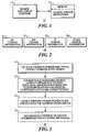
- FIG. 1comprises a block diagram as configured in accordance with various embodiments of the invention
- FIG. 2comprises a schematic representation as configured in accordance with various embodiments of the invention
- FIG. 3comprises a flow diagram as configured in accordance with various embodiments of the invention.
- FIG. 4comprises a schematic representation as configured in accordance with various embodiments of the invention.
- FIG. 5comprises a schematic representation as configured in accordance with various embodiments of the invention.
- an enabling processdetects a change in the operational status of a mobile station during a communication session and, in response to detecting that change, automatically increases memory capacity that is available to support additional communication sessions while simultaneously persisting at least some session information from that communication session for potential subsequent use during that communication session.
- this processdetects, in particular, a change in operational status from an active status to a dormant status though other approaches are available and may be preferable in a given setting.
- session context informationas corresponds to that communication session is deleted.
- the retained session context informationis then stored. This stored information can then be quickly retrieved should the mobile station again become active in this communication session.
- the retained session content information(in whole or in part) can be compressed prior to storing such information.
- critical and/or useful session content informationcan persist and be available to quickly facilitate subsequent participation of the mobile station in a given communication session while also effecting a dynamic and significant increase in the quantity of available memory. This, in turn, can lead to a significant increase in the number of calls that can be supported by a given network element as the average storage requirements per call will typically drop.
- a network element 10such as, but not limited to, a Packet Data Serving Node, a Serving General Packet Radio Service (GPRS) Support Node, a Home Agent, a Gateway GPRS Support Node, and the like.
- GPRSGeneral Packet Radio Service
- Such a network element 10comprises, in relevant part, a communication session facilitation platform 11 that operably couples to (or includes, in whole or in part) a memory 12 .
- the memory 12has session context information stored therein. More particularly, and as will be explained below in more detail, from time to time and during the course of a given communication session for a given mobile station, this session context information comprises an incomplete set of session context information as corresponds to that communication session. In a preferred approach, this incomplete set of session context information comprises, at the least, a minimal necessary subset of information as is necessary to facilitate subsequent restoration of a given call.
- This memory 12can be realized in any of a wide variety of ways.
- this memory 12can comprise a centralized storage platform or, if desired, the storage role can be distributed over a larger number of platforms.
- this memorycan be integral to the network element 10 or, if desired, some or all of the storage role described herein can be assigned to a more remotely located memory.
- Such architectural optionsare well understood in the art and require no further description here.
- Network elementstypically comprise a partially or wholly programmable platform.
- this programming and/or configurationcan comprise provision of a session facilitation platform 11 that can detect a change in operational status of a given mobile station during the course of a communication session and, in response to detecting that change, automatically increase memory capacity that is available to support additional communication sessions while simultaneously persisting some session information for potential subsequent use during the communication session.
- the session facilitation platform 11stores such session information in the memory 12 as the incomplete set of session context information noted above.
- the session facilitation platform 11can also detect another change in the operational status of the given mobile station during that communication session (such as, and again as will be described below in more detail, a change from a dormant to an active mode of operation) and, in response to detecting that change, can automatically retrieve the incomplete set of session information for use during the communication session to at least substantially recreate a complete session context for the given mobile station.
- another change in the operational status of the given mobile station during that communication sessionsuch as, and again as will be described below in more detail, a change from a dormant to an active mode of operation
- the session context information 20will of course vary from application to application.
- such session context information 20will comprise Radio Network Node (RNN) to Packet Data Serving Node (PDSN) (RP) protocol session information 21 (such as, but not limited to user name, Packet Control Function addressing, GRE key values, IMSI values, and the like), Point-to-Point Protocol (PPP) session information 22 (such as, but not limited to, Link Control Protocol information, ACCM mapping, compression values or information, Domain Name server values, and the like), Internet Protocol (IP) session information 23 (such as, but not limited to IP addresses, internal state information, and the like), and such other session information 24 as may be relevant and applicable in a given setting (such as, but not limited to, mobile IP flags and/or identification, accounting information (regarding, for example, prepaid services, roaming arrangements, quality of service, and so forth), and the like).
- RNNRadio Network Node
- PDSNPacket Data Serving Node
- RPPacket Data Serving Node
- these teachingsencompass generally a process 30 that provides for detection 31 of a change in the operational status of a mobile station during a communication session.
- This changecan constitute, for example, a change in operational status from active status to dormant status.
- this process 10can effect such detection. For example, if desired, locally stored non-compressed triggering information can be employed for this purpose.
- this process 10can access presence information regarding the mobile station (as may be available, for example, via a presence server) when such presence information reflects the operational change of interest.
- this detectioncan comprise receiving a message indicating the change in operational status.
- the enabling network elementcan receive a Radio Network Node (RNN) to Packet Data Serving Node (PDSN) (RP) protocol compatible message in this regard (such as, to illustrate, an ACTIVE_STOP message over an A11 control channel, though other parameters will do doubt be appropriate to use to generate such a trigger in other systems as will be well understood by those skilled in the art).
- RNNRadio Network Node
- RPPacket Data Serving Node
- this detectioncan comprise detecting the conclusion of an inactivity duration of time.
- the network elementor a surrogate acting on its behalf
- can initiate a timerby beginning a countdown or incrementing a count
- the persistent inactivity of the mobile stationcan be used to detect the mobile station as now being in a dormant state of operation.
- historical information(regarding, for example, the active and inactive behaviors of the mobile station) may also be used to inform, directly or indirectly, such a detection process.
- This process 30then provides for automatically increasing 32 memory capacity that is available to support available communication sessions while simultaneously persisting at least some session information for potential subsequent use during the communication session.
- Memory capacitycan be so increased using any of a wide variety of techniques.
- memory capacitycan be increased by compressing at least some of the previously stored session information. This can comprise compressing some, or all, of the previously stored session information.
- memory capacitycan be so increased by deleting at least some, but not all, of the session context information as corresponds to the communication session. More particularly, previously stored session information that is not critical to subsequent restoration of a corresponding call can be so deleted.
- memory capacityis increased by deleting at least some, but not all, session context information as corresponds to the communication session to thereby provide some resultant retained session context information, and then compressing at least some of the retained session context information to provide compressed retained session context information.
- This reduced and compressed quantity of informationcan then be stored in a memory that also stores session context information to support additional communication sessions and/or in a memory that is discrete from a memory that stores such session context information, as may best suit the needs of a given context or application.
- the network elementsignificantly reduces through deletion and/or compression the amount of session context information that is retained by (or on behalf of) the network element notwithstanding that the communication session has not concluded. This, in turn, results in memory space that would otherwise have been allocated during such a session. This additional memory space can be used to support additional calls, thereby increasing the number of calls that can be handled and supported by a single network element.
- the particular information that persistscan vary with the particular application. In general, such information will preferably comprise any kind of information that is usable at a later time to facilitate call restoration including particularly relevant session context information. Such information can comprise, for example, Radio Network Node to Packet Data Serving Node protocol session context information, Point-to-Point Protocol session context information, Internet Protocol session context information, or some relevant combination thereof.
- this process 30can further comprise then detecting 33 another change in the operational status of the mobile station during the communication session (for example, a change from a dormant status to an active status). Upon detecting such a change, the process 30 can then automatically retrieve 34 at least some of the stored session information to use during the communication session. This retrieval can be effected with respect to whichever local or remote memory (or memories) contains such information. In a preferred embodiment, this comprises retrieving session context information comprising, for example, any of Radio Network Node to Packet Data Serving Node protocol session context information, Point-to-Point Protocol session context information, Internet Protocol session context information, or some combination thereof.
- Such retrievalcan also comprise, when the information has been previously compressed as described above, the automatic decompression of at least a part of such stored session information.
- the network elementcan utilize the recovered session context information to reconstruct or otherwise restore a desired level of connectivity for the mobile station at such time as the mobile station shifts from a dormant to an active status. This occurs notwithstanding that the network element had previously deleted and/or compressed the relevant information in order to make room available to accommodate an increased quantity of other communication sessions.
- FIG. 4provides an illustrative schematic view of deleting such previously stored session information.
- the session information 40comprises RP session information, PPP session information, IP session information, and other session information.
- a first quantity 42 of RP session information(comprising, in a preferred embodiment, RP session information that is not critical to reestablishment of the corresponding call) is discarded, leaving a reduced quantity 41 of persisted RP session information.
- a reduced quantity 43 of persisted PPP session information, a reduced quantity 44 of persisted IP session information, and a reduced quantity 45 of other session informationis provided.
- these reduced quantities of informationcan be stored and some significant amount of memory will be rendered available to support other sessions.
- the above-described persisted information 51can be compressed to provide a resultant quantity of persisted and compressed session information 52 .
- Numerous compression techniquesare presently known and others will no doubt be developed in the future. These teachings are not particularly sensitive to use or selection of any particular compression technique and hence these teachings may be viewed as being applicable in combination with all such compression techniques.
Landscapes
- Engineering & Computer Science (AREA)
- Computer Networks & Wireless Communication (AREA)
- Signal Processing (AREA)
- Chemical & Material Sciences (AREA)
- Nanotechnology (AREA)
- Physics & Mathematics (AREA)
- Mathematical Physics (AREA)
- Theoretical Computer Science (AREA)
- Crystallography & Structural Chemistry (AREA)
- Data Exchanges In Wide-Area Networks (AREA)
- Mobile Radio Communication Systems (AREA)
Abstract
Description
- This invention relates generally to call processing in a communication system and more particularly to memory management of call-related information.
- Using a network element such as a Packet Data Serving Node (PDSN) to facilitate a communication is well known in the art. This includes, in more recent times, supporting communication sessions such as voice and/or data calls as between two or more parties. In many cases, the number of calls that a given network element can support at any given time is less than the network as a whole might otherwise support. As a result, a plurality of such network elements are typically deployed in order to make effective use of a given network's available resources.
- There are, however, various causes contributing to the limited call capacity of a network element. One important causative agent comprises available memory. To illustrate, when a new call arrives at a Packet Data Serving Node, different modules as comprise the Packet Data Serving Node each allocate memory to store corresponding call context information. A not untypical Packet Data Serving Node chassis, for example, allocates about 30 KB of memory for each call for these purposes. As a result, many Packet Data Serving Nodes can only support a maximum of about 40,000 calls per card.
- One can, of course, increase available memory by increasing the available quantity of memory. In many cases, however, this approach is unattractive. Increasing memory may, in some cases, be physically impossible. In other cases it may represent an unacceptable increase in cost.
- The above needs are at least partially met through provision of the method and apparatus to increase session capacity described in the following detailed description, particularly when studied in conjunction with the drawings, wherein:
FIG. 1 comprises a block diagram as configured in accordance with various embodiments of the invention;FIG. 2 comprises a schematic representation as configured in accordance with various embodiments of the invention;FIG. 3 comprises a flow diagram as configured in accordance with various embodiments of the invention;FIG. 4 comprises a schematic representation as configured in accordance with various embodiments of the invention; andFIG. 5 comprises a schematic representation as configured in accordance with various embodiments of the invention.- Skilled artisans will appreciate that elements in the figures are illustrated for simplicity and clarity and have not necessarily been drawn to scale. For example, the dimensions of some of the elements in the figures may be exaggerated relative to other elements to help to improve understanding of various embodiments of the present invention. Also, common but well-understood elements that are useful or necessary in a commercially feasible embodiment are often not depicted in order to facilitate a less obstructed view of these various embodiments of the present invention. It will also be understood that the terms and expressions used herein have the ordinary meaning as is usually accorded to such terms and expressions by those skilled in the corresponding respective areas of inquiry and study except where other specific meanings have otherwise been set forth herein.
- Generally speaking, pursuant to these various embodiments, an enabling process detects a change in the operational status of a mobile station during a communication session and, in response to detecting that change, automatically increases memory capacity that is available to support additional communication sessions while simultaneously persisting at least some session information from that communication session for potential subsequent use during that communication session.
- In a preferred approach, this process detects, in particular, a change in operational status from an active status to a dormant status though other approaches are available and may be preferable in a given setting.
- There are, also, various ways to effect the indicated increase in memory capacity. Pursuant to one approach, some, but not all, session context information as corresponds to that communication session is deleted. The retained session context information is then stored. This stored information can then be quickly retrieved should the mobile station again become active in this communication session. Pursuant to a related approach, the retained session content information (in whole or in part) can be compressed prior to storing such information.
- So configured, critical and/or useful session content information can persist and be available to quickly facilitate subsequent participation of the mobile station in a given communication session while also effecting a dynamic and significant increase in the quantity of available memory. This, in turn, can lead to a significant increase in the number of calls that can be supported by a given network element as the average storage requirements per call will typically drop.
- These and other benefits may become more evident upon making a thorough review and study of the following detailed description. Referring now to the drawings, and in particular to
FIG. 1 , these teachings can be implemented in various ways but are preferably, at this time, carried forth by anetwork element 10 such as, but not limited to, a Packet Data Serving Node, a Serving General Packet Radio Service (GPRS) Support Node, a Home Agent, a Gateway GPRS Support Node, and the like. Such anetwork element 10 comprises, in relevant part, a communicationsession facilitation platform 11 that operably couples to (or includes, in whole or in part) amemory 12. - The
memory 12 has session context information stored therein. More particularly, and as will be explained below in more detail, from time to time and during the course of a given communication session for a given mobile station, this session context information comprises an incomplete set of session context information as corresponds to that communication session. In a preferred approach, this incomplete set of session context information comprises, at the least, a minimal necessary subset of information as is necessary to facilitate subsequent restoration of a given call. - This
memory 12 can be realized in any of a wide variety of ways. For example, thismemory 12 can comprise a centralized storage platform or, if desired, the storage role can be distributed over a larger number of platforms. Further, this memory can be integral to thenetwork element 10 or, if desired, some or all of the storage role described herein can be assigned to a more remotely located memory. Such architectural options are well understood in the art and require no further description here. - Network elements, including Packet Data Serving Nodes, typically comprise a partially or wholly programmable platform. Those skilled in the art will recognize and understand that such a platform can be readily programmed, configured, and arranged to accord with these teachings. More particularly, this programming and/or configuration can comprise provision of a
session facilitation platform 11 that can detect a change in operational status of a given mobile station during the course of a communication session and, in response to detecting that change, automatically increase memory capacity that is available to support additional communication sessions while simultaneously persisting some session information for potential subsequent use during the communication session. More particularly, in a preferred approach thesession facilitation platform 11 stores such session information in thememory 12 as the incomplete set of session context information noted above. - Further, and also pursuant to a preferred approach, the
session facilitation platform 11 can also detect another change in the operational status of the given mobile station during that communication session (such as, and again as will be described below in more detail, a change from a dormant to an active mode of operation) and, in response to detecting that change, can automatically retrieve the incomplete set of session information for use during the communication session to at least substantially recreate a complete session context for the given mobile station. - With reference to
FIG. 2 , thesession context information 20 will of course vary from application to application. In a not untypical setting, however, suchsession context information 20 will comprise Radio Network Node (RNN) to Packet Data Serving Node (PDSN) (RP) protocol session information21 (such as, but not limited to user name, Packet Control Function addressing, GRE key values, IMSI values, and the like), Point-to-Point Protocol (PPP) session information22 (such as, but not limited to, Link Control Protocol information, ACCM mapping, compression values or information, Domain Name server values, and the like), Internet Protocol (IP) session information23 (such as, but not limited to IP addresses, internal state information, and the like), and suchother session information 24 as may be relevant and applicable in a given setting (such as, but not limited to, mobile IP flags and/or identification, accounting information (regarding, for example, prepaid services, roaming arrangements, quality of service, and so forth), and the like). Such session context information comprises a generally well-understand aspect of present practice and therefore additional elaboration will not be provided here for the sake of brevity. - Referring now to
FIG. 3 , these teachings encompass generally aprocess 30 that provides fordetection 31 of a change in the operational status of a mobile station during a communication session. This change can constitute, for example, a change in operational status from active status to dormant status. There are various ways by which thisprocess 10 can effect such detection. For example, if desired, locally stored non-compressed triggering information can be employed for this purpose. As another example, thisprocess 10 can access presence information regarding the mobile station (as may be available, for example, via a presence server) when such presence information reflects the operational change of interest. - As yet another example, this detection can comprise receiving a message indicating the change in operational status. For example, the enabling network element can receive a Radio Network Node (RNN) to Packet Data Serving Node (PDSN) (RP) protocol compatible message in this regard (such as, to illustrate, an ACTIVE_STOP message over an A11 control channel, though other parameters will do doubt be appropriate to use to generate such a trigger in other systems as will be well understood by those skilled in the art).
- As yet another example, this detection can comprise detecting the conclusion of an inactivity duration of time. To illustrate, the network element (or a surrogate acting on its behalf) can initiate a timer (by beginning a countdown or incrementing a count) upon detecting inactivity on the part of the mobile station. When that timer concludes, the persistent inactivity of the mobile station can be used to detect the mobile station as now being in a dormant state of operation.
- Other possibilities exist as well. For example, historical information (regarding, for example, the active and inactive behaviors of the mobile station) may also be used to inform, directly or indirectly, such a detection process.
- This
process 30 then provides for automatically increasing32 memory capacity that is available to support available communication sessions while simultaneously persisting at least some session information for potential subsequent use during the communication session. Memory capacity can be so increased using any of a wide variety of techniques. As one example, memory capacity can be increased by compressing at least some of the previously stored session information. This can comprise compressing some, or all, of the previously stored session information. As another example, memory capacity can be so increased by deleting at least some, but not all, of the session context information as corresponds to the communication session. More particularly, previously stored session information that is not critical to subsequent restoration of a corresponding call can be so deleted. - In a preferred approach, memory capacity is increased by deleting at least some, but not all, session context information as corresponds to the communication session to thereby provide some resultant retained session context information, and then compressing at least some of the retained session context information to provide compressed retained session context information. This reduced and compressed quantity of information can then be stored in a memory that also stores session context information to support additional communication sessions and/or in a memory that is discrete from a memory that stores such session context information, as may best suit the needs of a given context or application.
- So configured, the network element significantly reduces through deletion and/or compression the amount of session context information that is retained by (or on behalf of) the network element notwithstanding that the communication session has not concluded. This, in turn, results in memory space that would otherwise have been allocated during such a session. This additional memory space can be used to support additional calls, thereby increasing the number of calls that can be handled and supported by a single network element. The particular information that persists can vary with the particular application. In general, such information will preferably comprise any kind of information that is usable at a later time to facilitate call restoration including particularly relevant session context information. Such information can comprise, for example, Radio Network Node to Packet Data Serving Node protocol session context information, Point-to-Point Protocol session context information, Internet Protocol session context information, or some relevant combination thereof.
- In an optional but preferred approach, this
process 30 can further comprise then detecting33 another change in the operational status of the mobile station during the communication session (for example, a change from a dormant status to an active status). Upon detecting such a change, theprocess 30 can then automatically retrieve 34 at least some of the stored session information to use during the communication session. This retrieval can be effected with respect to whichever local or remote memory (or memories) contains such information. In a preferred embodiment, this comprises retrieving session context information comprising, for example, any of Radio Network Node to Packet Data Serving Node protocol session context information, Point-to-Point Protocol session context information, Internet Protocol session context information, or some combination thereof. - Such retrieval can also comprise, when the information has been previously compressed as described above, the automatic decompression of at least a part of such stored session information.
- So configured, the network element can utilize the recovered session context information to reconstruct or otherwise restore a desired level of connectivity for the mobile station at such time as the mobile station shifts from a dormant to an active status. This occurs notwithstanding that the network element had previously deleted and/or compressed the relevant information in order to make room available to accommodate an increased quantity of other communication sessions.
FIG. 4 provides an illustrative schematic view of deleting such previously stored session information. In this representative depiction, thesession information 40 comprises RP session information, PPP session information, IP session information, and other session information. In this illustration, afirst quantity 42 of RP session information (comprising, in a preferred embodiment, RP session information that is not critical to reestablishment of the corresponding call) is discarded, leaving a reducedquantity 41 of persisted RP session information. In a similar fashion, a reducedquantity 43 of persisted PPP session information, a reducedquantity 44 of persisted IP session information, and a reducedquantity 45 of other session information is provided. At this point, if desired, these reduced quantities of information can be stored and some significant amount of memory will be rendered available to support other sessions.- If desired, and referring now to
FIG. 5 , the above-described persistedinformation 51 can be compressed to provide a resultant quantity of persisted andcompressed session information 52. Numerous compression techniques are presently known and others will no doubt be developed in the future. These teachings are not particularly sensitive to use or selection of any particular compression technique and hence these teachings may be viewed as being applicable in combination with all such compression techniques. - In the more specific illustrative examples provided above, RP, PPP, and IP session context information was presented as examples of session specific information of interest. Those skilled in the art will appreciate that any information deemed critical to call restoration can be similarly identified and processed to achieve or maintain the benefits set for herein.
- Those skilled in the art will appreciate that considerable memory savings can be achieved using these teachings and that these savings can be directly applied in favor of supporting additional communication sessions. This, in turn, permits an existing network element such as a Packet Data Serving Node to be further leveraged with respect to the number of communication sessions that such a network element might otherwise be expected to reasonably accommodate. At the same time, these benefits are not gained at the undue expense of delay or inefficiency with respect to supporting subsequent participation of a given mobile station in a later portion of a given communication session, as the network element has the requisite core of information necessary to effect, for example, a rapid shift to reflect a change by the mobile station from a dormant status to an active status.
- Those skilled in the art will recognize that a wide variety of modifications, alterations, and combinations can be made with respect to the above described embodiments without departing from the spirit and scope of the invention, and that such modifications, alterations, and combinations are to be viewed as being within the ambit of the inventive concept.
Claims (21)
1-125. (canceled)
126. A method, comprising:
providing a semiconductor nanoscale wire;
patterning a mask on the nanoscale wire to define at least a first portion not covered by the mask and a second portion covered by the mask;
exposing the first portion but not the second portion to a bulk metal; and
diffusing at least a portion of the bulk metal into the first portion of the nanoscale wire.
127. The method ofclaim 126 , wherein the semiconductor nanoscale wire comprises silicon.
128. The method ofclaim 127 , comprising diffusing at least a portion of the bulk metal into the first portion of the nanoscale wire to form a metal silicide having a stoichiometric ratio of silicon and at least one metal.
129. The method ofclaim 128 , wherein the metal silicide comprises nickel silicide.
130. The method ofclaim 126 , wherein the bulk metal comprises a transition metal.
131. The method ofclaim 126 , wherein the bulk metal comprises nickel.
132. The method ofclaim 126 , wherein the first portion of the nanoscale wire has a smallest dimension less than 200 nm.
133. The method ofclaim 126 , wherein the nanoscale wire is a single crystal.
134. The method ofclaim 126 , wherein the mask comprises photoresist.
135. The method ofclaim 126 , wherein the mask comprises a second nanoscale wire.
136. The method ofclaim 135 , wherein the second nanoscale wire comprises a core and a shell.
137. The method ofclaim 126 , wherein the nanoscale wire is a nanowire.
138. The method ofclaim 126 , comprising diffusing at least a portion of the bulk metal into the first portion of the nanoscale wire such that the first region has a resistivity of less than about 60 microOhm cm.
139. The method ofclaim 126 , comprising diffusing at least a portion of the bulk metal into the first portion of the nanoscale wire such that the first region is able to carry a current density of at least about 108A/cm2.
140. A method, comprising:
promoting a method comprising an act of diffusing at least a portion of a bulk metal into at least a portion of a semiconductor nanoscale wire, the bulk metal and the semiconductor nanoscale wire being adjacent, wherein the semiconductor nanoscale wire comprises at least one portion having a smallest dimension of less than about 500 nm.
141. The method ofclaim 140 , wherein the bulk metal comprises nickel.
142. The method ofclaim 140 , wherein the semiconductor nanoscale wire comprises silicon.
143. The method ofclaim 140 , comprising promoting a method comprising an act of diffusing at least a portion of the bulk metal into at least a portion of the semiconductor wire to form a metal silicide.
144. The method ofclaim 143 , wherein the metal silicide has a stoichiometric ratio of silicon and at least one metal.
145. The method ofclaim 144 , wherein the metal silicide comprises nickel silicide.
Priority Applications (1)
| Application Number | Priority Date | Filing Date | Title |
|---|---|---|---|
| US10/588,833US20090227107A9 (en) | 2004-02-13 | 2005-02-14 | Nanostructures Containing Metal Semiconductor Compounds |
Applications Claiming Priority (5)
| Application Number | Priority Date | Filing Date | Title |
|---|---|---|---|
| US54480004P | 2004-02-13 | 2004-02-13 | |
| US57996704P | 2004-06-15 | 2004-06-15 | |
| US11018299 | 2004-12-21 | ||
| PCT/US2005/004459WO2005093831A1 (en) | 2004-02-13 | 2005-02-14 | Nanostructures containing metal-semiconductor compounds |
| US10/588,833US20090227107A9 (en) | 2004-02-13 | 2005-02-14 | Nanostructures Containing Metal Semiconductor Compounds |
Publications (2)
| Publication Number | Publication Date |
|---|---|
| US20090004852A1true US20090004852A1 (en) | 2009-01-01 |
| US20090227107A9 US20090227107A9 (en) | 2009-09-10 |
Family
ID=41064565
Family Applications (1)
| Application Number | Title | Priority Date | Filing Date |
|---|---|---|---|
| US10/588,833AbandonedUS20090227107A9 (en) | 2004-02-13 | 2005-02-14 | Nanostructures Containing Metal Semiconductor Compounds |
Country Status (1)
| Country | Link |
|---|---|
| US (1) | US20090227107A9 (en) |
Cited By (21)
| Publication number | Priority date | Publication date | Assignee | Title |
|---|---|---|---|---|
| US20070026645A1 (en)* | 2000-08-22 | 2007-02-01 | President And Fellows Of Harvard College | Doped elongated semiconductors, growing such semiconductors, devices including such semiconductors, and fabricating such devices |
| US20070264623A1 (en)* | 2004-06-15 | 2007-11-15 | President And Fellows Of Harvard College | Nanosensors |
| US20070281156A1 (en)* | 2000-08-22 | 2007-12-06 | President And Fellows Of Harvard College | Nanoscale wires and related devices |
| US20080191196A1 (en)* | 2005-06-06 | 2008-08-14 | Wei Lu | Nanowire heterostructures |
| US20090057650A1 (en)* | 2000-08-22 | 2009-03-05 | President And Fellows Of Harvard College | Nanoscale wires and related devices |
| US20090095950A1 (en)* | 2004-12-06 | 2009-04-16 | President And Fellows Of Harvard College | Nanoscale Wire-Based Data Storage |
| US20090227107A9 (en)* | 2004-02-13 | 2009-09-10 | President And Fellows Of Havard College | Nanostructures Containing Metal Semiconductor Compounds |
| US20100087013A1 (en)* | 2006-06-12 | 2010-04-08 | President And Fellows Of Harvard College | Nanosensors and related technologies |
| US20100152057A1 (en)* | 2006-11-22 | 2010-06-17 | President And Fellows Of Havard College | High-sensitivity nanoscale wire sensors |
| CN101783367A (en)* | 2010-02-11 | 2010-07-21 | 复旦大学 | Nanowire MOS transistor based on III-V element and preparation method thereof |
| US7956427B2 (en) | 2000-12-11 | 2011-06-07 | President And Fellows Of Harvard College | Nanosensors |
| US8058640B2 (en) | 2006-09-11 | 2011-11-15 | President And Fellows Of Harvard College | Branched nanoscale wires |
| US8232584B2 (en) | 2005-05-25 | 2012-07-31 | President And Fellows Of Harvard College | Nanoscale sensors |
| WO2014043341A1 (en) | 2012-09-12 | 2014-03-20 | President And Fellows Of Harvard College | Nanoscale field-effect transistors for biomolecular sensors and other applications |
| US9297796B2 (en) | 2009-09-24 | 2016-03-29 | President And Fellows Of Harvard College | Bent nanowires and related probing of species |
| US9390951B2 (en) | 2009-05-26 | 2016-07-12 | Sharp Kabushiki Kaisha | Methods and systems for electric field deposition of nanowires and other devices |
| US9559193B2 (en) | 2011-04-22 | 2017-01-31 | Semiconductor Energy Laboratory Co., Ltd. | Semiconductor device and method for manufacturing semiconductor device |
| US9660095B2 (en) | 2011-04-22 | 2017-05-23 | Semiconductor Energy Laboratory Co., Ltd. | Semiconductor device |
| US20170290619A1 (en)* | 2013-03-07 | 2017-10-12 | Arthrocare Corporation | Methods and systems related to electrosurgical wands |
| US20180088079A1 (en)* | 2015-04-03 | 2018-03-29 | President And Fellows Of Harvard College | Nanoscale wires with external layers for sensors and other applications |
| CN114364056A (en)* | 2021-12-28 | 2022-04-15 | 天翼物联科技有限公司 | Method, system, device and storage medium for controlling terminal LWM2M session |
Families Citing this family (1)
| Publication number | Priority date | Publication date | Assignee | Title |
|---|---|---|---|---|
| CN104835817B (en)* | 2014-02-08 | 2018-03-30 | 中芯国际集成电路制造(上海)有限公司 | A kind of semiconductor devices and its manufacture method |
Citations (83)
| Publication number | Priority date | Publication date | Assignee | Title |
|---|---|---|---|---|
| US3873360A (en)* | 1971-11-26 | 1975-03-25 | Western Electric Co | Method of depositing a metal on a surface of a substrate |
| US3873359A (en)* | 1971-11-26 | 1975-03-25 | Western Electric Co | Method of depositing a metal on a surface of a substrate |
| US4673474A (en)* | 1984-10-16 | 1987-06-16 | Matsushita Electric Industrial Co., Ltd. | Molecular controlled structure and method of producing the same |
| US5023139A (en)* | 1989-04-04 | 1991-06-11 | Research Corporation Technologies, Inc. | Nonlinear optical materials |
| US5089545A (en)* | 1989-02-12 | 1992-02-18 | Biotech International, Inc. | Switching and memory elements from polyamino acids and the method of their assembly |
| US5512131A (en)* | 1993-10-04 | 1996-04-30 | President And Fellows Of Harvard College | Formation of microstamped patterns on surfaces and derivative articles |
| US5524092A (en)* | 1995-02-17 | 1996-06-04 | Park; Jea K. | Multilayered ferroelectric-semiconductor memory-device |
| US5607876A (en)* | 1991-10-28 | 1997-03-04 | Xerox Corporation | Fabrication of quantum confinement semiconductor light-emitting devices |
| US5620850A (en)* | 1994-09-26 | 1997-04-15 | President And Fellows Of Harvard College | Molecular recognition at surfaces derivatized with self-assembled monolayers |
| US5640343A (en)* | 1996-03-18 | 1997-06-17 | International Business Machines Corporation | Magnetic memory array using magnetic tunnel junction devices in the memory cells |
| US5726524A (en)* | 1996-05-31 | 1998-03-10 | Minnesota Mining And Manufacturing Company | Field emission device having nanostructured emitters |
| US5739057A (en)* | 1995-11-06 | 1998-04-14 | Tiwari; Sandip | Method of making self-aligned dual gate MOSFET with an ultranarrow channel |
| US5747180A (en)* | 1995-05-19 | 1998-05-05 | University Of Notre Dame Du Lac | Electrochemical synthesis of quasi-periodic quantum dot and nanostructure arrays |
| US5751156A (en)* | 1995-06-07 | 1998-05-12 | Yale University | Mechanically controllable break transducer |
| US5858862A (en)* | 1996-09-25 | 1999-01-12 | Sony Corporation | Process for producing quantum fine wire |
| US5864823A (en)* | 1997-06-25 | 1999-01-26 | Virtel Corporation | Integrated virtual telecommunication system for E-commerce |
| US5866434A (en)* | 1994-12-08 | 1999-02-02 | Meso Scale Technology | Graphitic nanotubes in luminescence assays |
| US5882779A (en)* | 1994-11-08 | 1999-03-16 | Spectra Science Corporation | Semiconductor nanocrystal display materials and display apparatus employing same |
| US5897945A (en)* | 1996-02-26 | 1999-04-27 | President And Fellows Of Harvard College | Metal oxide nanorods |
| US5900160A (en)* | 1993-10-04 | 1999-05-04 | President And Fellows Of Harvard College | Methods of etching articles via microcontact printing |
| US5903010A (en)* | 1997-10-29 | 1999-05-11 | Hewlett-Packard Company | Quantum wire switch and switching method |
| US5908692A (en)* | 1997-01-23 | 1999-06-01 | Wisconsin Alumni Research Foundation | Ordered organic monolayers and methods of preparation thereof |
| US5916642A (en)* | 1995-11-22 | 1999-06-29 | Northwestern University | Method of encapsulating a material in a carbon nanotube |
| US6036774A (en)* | 1996-02-26 | 2000-03-14 | President And Fellows Of Harvard College | Method of producing metal oxide nanorods |
| US6038060A (en)* | 1997-01-16 | 2000-03-14 | Crowley; Robert Joseph | Optical antenna array for harmonic generation, mixing and signal amplification |
| US6069380A (en)* | 1997-07-25 | 2000-05-30 | Regents Of The University Of Minnesota | Single-electron floating-gate MOS memory |
| US6180239B1 (en)* | 1993-10-04 | 2001-01-30 | President And Fellows Of Harvard College | Microcontact printing on surfaces and derivative articles |
| US6187165B1 (en)* | 1997-10-02 | 2001-02-13 | The John Hopkins University | Arrays of semi-metallic bismuth nanowires and fabrication techniques therefor |
| US6190634B1 (en)* | 1995-06-07 | 2001-02-20 | President And Fellows Of Harvard College | Carbide nanomaterials |
| US6203864B1 (en)* | 1998-06-08 | 2001-03-20 | Nec Corporation | Method of forming a heterojunction of a carbon nanotube and a different material, method of working a filament of a nanotube |
| US6207392B1 (en)* | 1997-11-25 | 2001-03-27 | The Regents Of The University Of California | Semiconductor nanocrystal probes for biological applications and process for making and using such probes |
| US6211464B1 (en)* | 1998-05-20 | 2001-04-03 | Yazaki Corporation | Grommet having resilient flange for mounting on a panel |
| US6231744B1 (en)* | 1997-04-24 | 2001-05-15 | Massachusetts Institute Of Technology | Process for fabricating an array of nanowires |
| US6248674B1 (en)* | 2000-02-02 | 2001-06-19 | Hewlett-Packard Company | Method of aligning nanowires |
| US6340822B1 (en)* | 1999-10-05 | 2002-01-22 | Agere Systems Guardian Corp. | Article comprising vertically nano-interconnected circuit devices and method for making the same |
| US20020013031A1 (en)* | 1999-02-09 | 2002-01-31 | Kuen-Jian Chen | Method of improving the reliability of gate oxide layer |
| US6346189B1 (en)* | 1998-08-14 | 2002-02-12 | The Board Of Trustees Of The Leland Stanford Junior University | Carbon nanotube structures made using catalyst islands |
| US6355198B1 (en)* | 1996-03-15 | 2002-03-12 | President And Fellows Of Harvard College | Method of forming articles including waveguides via capillary micromolding and microtransfer molding |
| US20020040805A1 (en)* | 2000-02-04 | 2002-04-11 | Swager Timothy M. | Insulated nanoscopic pathways, compositions and devices of the same |
| US20020055239A1 (en)* | 2000-03-22 | 2002-05-09 | Mark Tuominen | Nanocylinder arrays |
| US20030003300A1 (en)* | 2001-07-02 | 2003-01-02 | Korgel Brian A. | Light-emitting nanoparticles and method of making same |
| US20030001091A1 (en)* | 2000-11-26 | 2003-01-02 | Yoshikazu Nakayama | Conductive probe for scanning microscope and machining method using the same |
| US6503375B1 (en)* | 2000-02-11 | 2003-01-07 | Applied Materials, Inc | Electroplating apparatus using a perforated phosphorus doped consumable anode |
| US20030032892A1 (en)* | 2001-04-25 | 2003-02-13 | Erlach Julian Van | Nanodevices, microdevices and sensors on in-vivo structures and method for the same |
| US20030048619A1 (en)* | 2001-06-15 | 2003-03-13 | Kaler Eric W. | Dielectrophoretic assembling of electrically functional microwires |
| US6538367B1 (en)* | 1999-07-15 | 2003-03-25 | Agere Systems Inc. | Field emitting device comprising field-concentrating nanoconductor assembly and method for making the same |
| US20030073071A1 (en)* | 2001-10-12 | 2003-04-17 | Jurgen Fritz | Solid state sensing system and method for measuring the binding or hybridization of biomolecules |
| US6559468B1 (en)* | 1999-03-29 | 2003-05-06 | Hewlett-Packard Development Company Lp | Molecular wire transistor (MWT) |
| US20030089899A1 (en)* | 2000-08-22 | 2003-05-15 | Lieber Charles M. | Nanoscale wires and related devices |
| US20030098488A1 (en)* | 2001-11-27 | 2003-05-29 | O'keeffe James | Band-structure modulation of nano-structures in an electric field |
| US20030113713A1 (en)* | 2001-09-10 | 2003-06-19 | Meso Scale Technologies, Llc | Methods and apparatus for conducting multiple measurements on a sample |
| US20030113940A1 (en)* | 2001-07-16 | 2003-06-19 | Erlanger Bernard F. | Antibodies specific for nanotubes and related methods and compositions |
| US20040005723A1 (en)* | 2002-04-02 | 2004-01-08 | Nanosys, Inc. | Methods of making, positioning and orienting nanostructures, nanostructure arrays and nanostructure devices |
| US20040026684A1 (en)* | 2002-04-02 | 2004-02-12 | Nanosys, Inc. | Nanowire heterostructures for encoding information |
| US6716409B2 (en)* | 2000-09-18 | 2004-04-06 | President And Fellows Of The Harvard College | Fabrication of nanotube microscopy tips |
| US20040067530A1 (en)* | 2002-05-08 | 2004-04-08 | The Regents Of The University Of California | Electronic sensing of biomolecular processes |
| US20040075464A1 (en)* | 2002-07-08 | 2004-04-22 | Btg International Limited | Nanostructures and methods for manufacturing the same |
| US20040095658A1 (en)* | 2002-09-05 | 2004-05-20 | Nanosys, Inc. | Nanocomposites |
| US6741019B1 (en)* | 1999-10-18 | 2004-05-25 | Agere Systems, Inc. | Article comprising aligned nanowires |
| US20050037374A1 (en)* | 1999-11-08 | 2005-02-17 | Melker Richard J. | Combined nanotechnology and sensor technologies for simultaneous diagnosis and treatment |
| US20050064731A1 (en)* | 2001-07-20 | 2005-03-24 | Hongkun Park | Transition metal oxide nanowires |
| US20050064185A1 (en)* | 2003-08-04 | 2005-03-24 | Nanosys, Inc. | System and process for producing nanowire composites and electronic substrates therefrom |
| US20050066883A1 (en)* | 2003-09-25 | 2005-03-31 | Nanosys, Inc. | Methods, devices and compositions for depositing and orienting nanostructures |
| US20050072213A1 (en)* | 2001-11-26 | 2005-04-07 | Isabelle Besnard | Use of id semiconductor materials as chemical sensing materials, produced and operated close to room temperature |
| US20050079659A1 (en)* | 2002-09-30 | 2005-04-14 | Nanosys, Inc. | Large-area nanoenabled macroelectronic substrates and uses therefor |
| US20050079533A1 (en)* | 1997-08-21 | 2005-04-14 | Samuelson Lynne A. | Enzymatic template polymerization |
| US6882051B2 (en)* | 2001-03-30 | 2005-04-19 | The Regents Of The University Of California | Nanowires, nanostructures and devices fabricated therefrom |
| US6882767B2 (en)* | 2001-12-27 | 2005-04-19 | The Regents Of The University Of California | Nanowire optoelectric switching device and method |
| US20050100960A1 (en)* | 2001-03-29 | 2005-05-12 | Hongjie Dai | Noncovalent sidewall functionalization of carbon nanotubes |
| US20050101026A1 (en)* | 2001-09-15 | 2005-05-12 | Sailor Michael J. | Photoluminescent polymetalloles as chemical sensors |
| US6897098B2 (en)* | 2003-07-28 | 2005-05-24 | Intel Corporation | Method of fabricating an ultra-narrow channel semiconductor device |
| US20050109989A1 (en)* | 2002-09-05 | 2005-05-26 | Nanosys, Inc. | Organic species that facilitate charge transfer to or from nanostructures |
| US6900479B2 (en)* | 2002-07-25 | 2005-05-31 | California Institute Of Technology | Stochastic assembly of sublithographic nanoscale interfaces |
| US20060009003A1 (en)* | 2004-07-07 | 2006-01-12 | Nanosys, Inc. | Methods for nanowire growth |
| US20060019472A1 (en)* | 2004-04-30 | 2006-01-26 | Nanosys, Inc. | Systems and methods for nanowire growth and harvesting |
| US6998333B2 (en)* | 2002-03-22 | 2006-02-14 | Hewlett-Packard Development Company, L.P. | Method for making nanoscale wires and gaps for switches and transistors |
| US20060054936A1 (en)* | 2000-12-11 | 2006-03-16 | President And Fellows Of Harvard College | Nanosensors |
| US20060057360A1 (en)* | 2003-11-26 | 2006-03-16 | Samuelson Lars I | Nanostructures formed of branched nanowhiskers and methods of producing the same |
| US7048903B2 (en)* | 1996-08-08 | 2006-05-23 | William Marsh Rice University | Macroscopically manipulable nanoscale devices made from nanotube assemblies |
| US20070026645A1 (en)* | 2000-08-22 | 2007-02-01 | President And Fellows Of Harvard College | Doped elongated semiconductors, growing such semiconductors, devices including such semiconductors, and fabricating such devices |
| US7172953B2 (en)* | 1999-07-02 | 2007-02-06 | President And Fellows Of Harvard College | Methods of forming nanoscopic wire-based devices and arrays |
| US7500213B2 (en)* | 2002-01-18 | 2009-03-03 | California Institute Of Technology | Array-based architecture for molecular electronics |
| US20090057650A1 (en)* | 2000-08-22 | 2009-03-05 | President And Fellows Of Harvard College | Nanoscale wires and related devices |
Family Cites Families (1)
| Publication number | Priority date | Publication date | Assignee | Title |
|---|---|---|---|---|
| US20090227107A9 (en)* | 2004-02-13 | 2009-09-10 | President And Fellows Of Havard College | Nanostructures Containing Metal Semiconductor Compounds |
- 2005
- 2005-02-14USUS10/588,833patent/US20090227107A9/ennot_activeAbandoned
Patent Citations (98)
| Publication number | Priority date | Publication date | Assignee | Title |
|---|---|---|---|---|
| US3873359A (en)* | 1971-11-26 | 1975-03-25 | Western Electric Co | Method of depositing a metal on a surface of a substrate |
| US3873360A (en)* | 1971-11-26 | 1975-03-25 | Western Electric Co | Method of depositing a metal on a surface of a substrate |
| US4673474A (en)* | 1984-10-16 | 1987-06-16 | Matsushita Electric Industrial Co., Ltd. | Molecular controlled structure and method of producing the same |
| US5089545A (en)* | 1989-02-12 | 1992-02-18 | Biotech International, Inc. | Switching and memory elements from polyamino acids and the method of their assembly |
| US5023139A (en)* | 1989-04-04 | 1991-06-11 | Research Corporation Technologies, Inc. | Nonlinear optical materials |
| US5607876A (en)* | 1991-10-28 | 1997-03-04 | Xerox Corporation | Fabrication of quantum confinement semiconductor light-emitting devices |
| US5512131A (en)* | 1993-10-04 | 1996-04-30 | President And Fellows Of Harvard College | Formation of microstamped patterns on surfaces and derivative articles |
| US6180239B1 (en)* | 1993-10-04 | 2001-01-30 | President And Fellows Of Harvard College | Microcontact printing on surfaces and derivative articles |
| US5900160A (en)* | 1993-10-04 | 1999-05-04 | President And Fellows Of Harvard College | Methods of etching articles via microcontact printing |
| US5620850A (en)* | 1994-09-26 | 1997-04-15 | President And Fellows Of Harvard College | Molecular recognition at surfaces derivatized with self-assembled monolayers |
| US5882779A (en)* | 1994-11-08 | 1999-03-16 | Spectra Science Corporation | Semiconductor nanocrystal display materials and display apparatus employing same |
| US5866434A (en)* | 1994-12-08 | 1999-02-02 | Meso Scale Technology | Graphitic nanotubes in luminescence assays |
| US5524092A (en)* | 1995-02-17 | 1996-06-04 | Park; Jea K. | Multilayered ferroelectric-semiconductor memory-device |
| US5747180A (en)* | 1995-05-19 | 1998-05-05 | University Of Notre Dame Du Lac | Electrochemical synthesis of quasi-periodic quantum dot and nanostructure arrays |
| US5751156A (en)* | 1995-06-07 | 1998-05-12 | Yale University | Mechanically controllable break transducer |
| US6190634B1 (en)* | 1995-06-07 | 2001-02-20 | President And Fellows Of Harvard College | Carbide nanomaterials |
| US5739057A (en)* | 1995-11-06 | 1998-04-14 | Tiwari; Sandip | Method of making self-aligned dual gate MOSFET with an ultranarrow channel |
| US5916642A (en)* | 1995-11-22 | 1999-06-29 | Northwestern University | Method of encapsulating a material in a carbon nanotube |
| US5897945A (en)* | 1996-02-26 | 1999-04-27 | President And Fellows Of Harvard College | Metal oxide nanorods |
| US6036774A (en)* | 1996-02-26 | 2000-03-14 | President And Fellows Of Harvard College | Method of producing metal oxide nanorods |
| US6355198B1 (en)* | 1996-03-15 | 2002-03-12 | President And Fellows Of Harvard College | Method of forming articles including waveguides via capillary micromolding and microtransfer molding |
| US5640343A (en)* | 1996-03-18 | 1997-06-17 | International Business Machines Corporation | Magnetic memory array using magnetic tunnel junction devices in the memory cells |
| US5726524A (en)* | 1996-05-31 | 1998-03-10 | Minnesota Mining And Manufacturing Company | Field emission device having nanostructured emitters |
| US7048903B2 (en)* | 1996-08-08 | 2006-05-23 | William Marsh Rice University | Macroscopically manipulable nanoscale devices made from nanotube assemblies |
| US5858862A (en)* | 1996-09-25 | 1999-01-12 | Sony Corporation | Process for producing quantum fine wire |
| US6038060A (en)* | 1997-01-16 | 2000-03-14 | Crowley; Robert Joseph | Optical antenna array for harmonic generation, mixing and signal amplification |
| US5908692A (en)* | 1997-01-23 | 1999-06-01 | Wisconsin Alumni Research Foundation | Ordered organic monolayers and methods of preparation thereof |
| US6231744B1 (en)* | 1997-04-24 | 2001-05-15 | Massachusetts Institute Of Technology | Process for fabricating an array of nanowires |
| US6359288B1 (en)* | 1997-04-24 | 2002-03-19 | Massachusetts Institute Of Technology | Nanowire arrays |
| US5864823A (en)* | 1997-06-25 | 1999-01-26 | Virtel Corporation | Integrated virtual telecommunication system for E-commerce |
| US6069380A (en)* | 1997-07-25 | 2000-05-30 | Regents Of The University Of Minnesota | Single-electron floating-gate MOS memory |
| US20050079533A1 (en)* | 1997-08-21 | 2005-04-14 | Samuelson Lynne A. | Enzymatic template polymerization |
| US6187165B1 (en)* | 1997-10-02 | 2001-02-13 | The John Hopkins University | Arrays of semi-metallic bismuth nanowires and fabrication techniques therefor |
| US6060724A (en)* | 1997-10-29 | 2000-05-09 | Hewlett-Packard Company | Quantum wire logic gate |
| US5903010A (en)* | 1997-10-29 | 1999-05-11 | Hewlett-Packard Company | Quantum wire switch and switching method |
| US6207392B1 (en)* | 1997-11-25 | 2001-03-27 | The Regents Of The University Of California | Semiconductor nanocrystal probes for biological applications and process for making and using such probes |
| US6211464B1 (en)* | 1998-05-20 | 2001-04-03 | Yazaki Corporation | Grommet having resilient flange for mounting on a panel |
| US6203864B1 (en)* | 1998-06-08 | 2001-03-20 | Nec Corporation | Method of forming a heterojunction of a carbon nanotube and a different material, method of working a filament of a nanotube |
| US6346189B1 (en)* | 1998-08-14 | 2002-02-12 | The Board Of Trustees Of The Leland Stanford Junior University | Carbon nanotube structures made using catalyst islands |
| US6528020B1 (en)* | 1998-08-14 | 2003-03-04 | The Board Of Trustees Of The Leland Stanford Junior University | Carbon nanotube devices |
| US20020013031A1 (en)* | 1999-02-09 | 2002-01-31 | Kuen-Jian Chen | Method of improving the reliability of gate oxide layer |
| US6559468B1 (en)* | 1999-03-29 | 2003-05-06 | Hewlett-Packard Development Company Lp | Molecular wire transistor (MWT) |
| US7172953B2 (en)* | 1999-07-02 | 2007-02-06 | President And Fellows Of Harvard College | Methods of forming nanoscopic wire-based devices and arrays |
| US6538367B1 (en)* | 1999-07-15 | 2003-03-25 | Agere Systems Inc. | Field emitting device comprising field-concentrating nanoconductor assembly and method for making the same |
| US6340822B1 (en)* | 1999-10-05 | 2002-01-22 | Agere Systems Guardian Corp. | Article comprising vertically nano-interconnected circuit devices and method for making the same |
| US6741019B1 (en)* | 1999-10-18 | 2004-05-25 | Agere Systems, Inc. | Article comprising aligned nanowires |
| US20050037374A1 (en)* | 1999-11-08 | 2005-02-17 | Melker Richard J. | Combined nanotechnology and sensor technologies for simultaneous diagnosis and treatment |
| US6248674B1 (en)* | 2000-02-02 | 2001-06-19 | Hewlett-Packard Company | Method of aligning nanowires |
| US20020040805A1 (en)* | 2000-02-04 | 2002-04-11 | Swager Timothy M. | Insulated nanoscopic pathways, compositions and devices of the same |
| US6503375B1 (en)* | 2000-02-11 | 2003-01-07 | Applied Materials, Inc | Electroplating apparatus using a perforated phosphorus doped consumable anode |
| US20020055239A1 (en)* | 2000-03-22 | 2002-05-09 | Mark Tuominen | Nanocylinder arrays |
| US20090057650A1 (en)* | 2000-08-22 | 2009-03-05 | President And Fellows Of Harvard College | Nanoscale wires and related devices |
| US20070032023A1 (en)* | 2000-08-22 | 2007-02-08 | President And Fellows Of Harvard College | Doped elongated semiconductors, growing such semiconductors, devices including such semiconductors, and fabricating such devices |
| US20070032052A1 (en)* | 2000-08-22 | 2007-02-08 | President And Fellows Of Harvard College | Doped elongated semiconductors, growing such semiconductors, devices including such semiconductors, and fabricating such devices |
| US20070032051A1 (en)* | 2000-08-22 | 2007-02-08 | President And Fellows Of Harvard College | Doped elongated semiconductors, growing such semiconductors, devices including such semiconductors, and fabricating such devices |
| US20030089899A1 (en)* | 2000-08-22 | 2003-05-15 | Lieber Charles M. | Nanoscale wires and related devices |
| US20070026645A1 (en)* | 2000-08-22 | 2007-02-01 | President And Fellows Of Harvard College | Doped elongated semiconductors, growing such semiconductors, devices including such semiconductors, and fabricating such devices |
| US20070048492A1 (en)* | 2000-08-22 | 2007-03-01 | President And Fellows Of Harvard College | Doped elongated semiconductors, growing such semiconductors, devices including such semiconductors, and fabricating such devices |
| US7211464B2 (en)* | 2000-08-22 | 2007-05-01 | President & Fellows Of Harvard College | Doped elongated semiconductors, growing such semiconductors, devices including such semiconductors and fabricating such devices |
| US7476596B2 (en)* | 2000-08-22 | 2009-01-13 | President And Fellows Of Harvard College | Doped elongated semiconductors, growing such semiconductors, devices including such semiconductors, and fabricating such devices |
| US6716409B2 (en)* | 2000-09-18 | 2004-04-06 | President And Fellows Of The Harvard College | Fabrication of nanotube microscopy tips |
| US20030001091A1 (en)* | 2000-11-26 | 2003-01-02 | Yoshikazu Nakayama | Conductive probe for scanning microscope and machining method using the same |
| US20060054936A1 (en)* | 2000-12-11 | 2006-03-16 | President And Fellows Of Harvard College | Nanosensors |
| US20050100960A1 (en)* | 2001-03-29 | 2005-05-12 | Hongjie Dai | Noncovalent sidewall functionalization of carbon nanotubes |
| US6882051B2 (en)* | 2001-03-30 | 2005-04-19 | The Regents Of The University Of California | Nanowires, nanostructures and devices fabricated therefrom |
| US6996147B2 (en)* | 2001-03-30 | 2006-02-07 | The Regents Of The University Of California | Methods of fabricating nanostructures and nanowires and devices fabricated therefrom |
| US20030032892A1 (en)* | 2001-04-25 | 2003-02-13 | Erlach Julian Van | Nanodevices, microdevices and sensors on in-vivo structures and method for the same |
| US20030048619A1 (en)* | 2001-06-15 | 2003-03-13 | Kaler Eric W. | Dielectrophoretic assembling of electrically functional microwires |
| US20030003300A1 (en)* | 2001-07-02 | 2003-01-02 | Korgel Brian A. | Light-emitting nanoparticles and method of making same |
| US6846565B2 (en)* | 2001-07-02 | 2005-01-25 | Board Of Regents, The University Of Texas System | Light-emitting nanoparticles and method of making same |
| US20030113940A1 (en)* | 2001-07-16 | 2003-06-19 | Erlanger Bernard F. | Antibodies specific for nanotubes and related methods and compositions |
| US20050064731A1 (en)* | 2001-07-20 | 2005-03-24 | Hongkun Park | Transition metal oxide nanowires |
| US20030113713A1 (en)* | 2001-09-10 | 2003-06-19 | Meso Scale Technologies, Llc | Methods and apparatus for conducting multiple measurements on a sample |
| US20050101026A1 (en)* | 2001-09-15 | 2005-05-12 | Sailor Michael J. | Photoluminescent polymetalloles as chemical sensors |
| US20030073071A1 (en)* | 2001-10-12 | 2003-04-17 | Jurgen Fritz | Solid state sensing system and method for measuring the binding or hybridization of biomolecules |
| US20050072213A1 (en)* | 2001-11-26 | 2005-04-07 | Isabelle Besnard | Use of id semiconductor materials as chemical sensing materials, produced and operated close to room temperature |
| US20030098488A1 (en)* | 2001-11-27 | 2003-05-29 | O'keeffe James | Band-structure modulation of nano-structures in an electric field |
| US6882767B2 (en)* | 2001-12-27 | 2005-04-19 | The Regents Of The University Of California | Nanowire optoelectric switching device and method |
| US7500213B2 (en)* | 2002-01-18 | 2009-03-03 | California Institute Of Technology | Array-based architecture for molecular electronics |
| US6998333B2 (en)* | 2002-03-22 | 2006-02-14 | Hewlett-Packard Development Company, L.P. | Method for making nanoscale wires and gaps for switches and transistors |
| US20040026684A1 (en)* | 2002-04-02 | 2004-02-12 | Nanosys, Inc. | Nanowire heterostructures for encoding information |
| US6872645B2 (en)* | 2002-04-02 | 2005-03-29 | Nanosys, Inc. | Methods of positioning and/or orienting nanostructures |
| US20040005723A1 (en)* | 2002-04-02 | 2004-01-08 | Nanosys, Inc. | Methods of making, positioning and orienting nanostructures, nanostructure arrays and nanostructure devices |
| US20040067530A1 (en)* | 2002-05-08 | 2004-04-08 | The Regents Of The University Of California | Electronic sensing of biomolecular processes |
| US7335908B2 (en)* | 2002-07-08 | 2008-02-26 | Qunano Ab | Nanostructures and methods for manufacturing the same |
| US20040075464A1 (en)* | 2002-07-08 | 2004-04-22 | Btg International Limited | Nanostructures and methods for manufacturing the same |
| US6900479B2 (en)* | 2002-07-25 | 2005-05-31 | California Institute Of Technology | Stochastic assembly of sublithographic nanoscale interfaces |
| US20040095658A1 (en)* | 2002-09-05 | 2004-05-20 | Nanosys, Inc. | Nanocomposites |
| US20050109989A1 (en)* | 2002-09-05 | 2005-05-26 | Nanosys, Inc. | Organic species that facilitate charge transfer to or from nanostructures |
| US20050110064A1 (en)* | 2002-09-30 | 2005-05-26 | Nanosys, Inc. | Large-area nanoenabled macroelectronic substrates and uses therefor |
| US20050079659A1 (en)* | 2002-09-30 | 2005-04-14 | Nanosys, Inc. | Large-area nanoenabled macroelectronic substrates and uses therefor |
| US6897098B2 (en)* | 2003-07-28 | 2005-05-24 | Intel Corporation | Method of fabricating an ultra-narrow channel semiconductor device |
| US20050064185A1 (en)* | 2003-08-04 | 2005-03-24 | Nanosys, Inc. | System and process for producing nanowire composites and electronic substrates therefrom |
| US20050066883A1 (en)* | 2003-09-25 | 2005-03-31 | Nanosys, Inc. | Methods, devices and compositions for depositing and orienting nanostructures |
| US20060057360A1 (en)* | 2003-11-26 | 2006-03-16 | Samuelson Lars I | Nanostructures formed of branched nanowhiskers and methods of producing the same |
| US20060019472A1 (en)* | 2004-04-30 | 2006-01-26 | Nanosys, Inc. | Systems and methods for nanowire growth and harvesting |
| US20060008942A1 (en)* | 2004-07-07 | 2006-01-12 | Nanosys, Inc. | Systems and methods for harvesting and integrating nanowires |
| US20060009003A1 (en)* | 2004-07-07 | 2006-01-12 | Nanosys, Inc. | Methods for nanowire growth |
Cited By (40)
| Publication number | Priority date | Publication date | Assignee | Title |
|---|---|---|---|---|
| US20070281156A1 (en)* | 2000-08-22 | 2007-12-06 | President And Fellows Of Harvard College | Nanoscale wires and related devices |
| US20070026645A1 (en)* | 2000-08-22 | 2007-02-01 | President And Fellows Of Harvard College | Doped elongated semiconductors, growing such semiconductors, devices including such semiconductors, and fabricating such devices |
| US20070032052A1 (en)* | 2000-08-22 | 2007-02-08 | President And Fellows Of Harvard College | Doped elongated semiconductors, growing such semiconductors, devices including such semiconductors, and fabricating such devices |
| US20070048492A1 (en)* | 2000-08-22 | 2007-03-01 | President And Fellows Of Harvard College | Doped elongated semiconductors, growing such semiconductors, devices including such semiconductors, and fabricating such devices |
| US20070252136A1 (en)* | 2000-08-22 | 2007-11-01 | President And Fellows Of Harvard College | Doped elongated semiconductors, growing such semiconductors, devices including such semiconductors and fabricating such devices |
| US20100093158A1 (en)* | 2000-08-22 | 2010-04-15 | President And Fellows Of Harvard College | Doped elongated semiconductors, growing such semiconductors, devices including such semiconductors and fabricating such devices |
| US20070032023A1 (en)* | 2000-08-22 | 2007-02-08 | President And Fellows Of Harvard College | Doped elongated semiconductors, growing such semiconductors, devices including such semiconductors, and fabricating such devices |
| US20090057650A1 (en)* | 2000-08-22 | 2009-03-05 | President And Fellows Of Harvard College | Nanoscale wires and related devices |
| US20100155698A1 (en)* | 2000-08-22 | 2010-06-24 | President And Fellows Of Harvard College | Nanoscale wires and related devices |
| US7915151B2 (en) | 2000-08-22 | 2011-03-29 | President And Fellows Of Harvard College | Doped elongated semiconductors, growing such semiconductors, devices including such semiconductors and fabricating such devices |
| US8153470B2 (en) | 2000-08-22 | 2012-04-10 | President And Fellows Of Harvard College | Doped elongated semiconductors, growing such semiconductors, devices including such semiconductors, and fabricating such devices |
| US7595260B2 (en) | 2000-08-22 | 2009-09-29 | President And Fellows Of Harvard College | Doped elongated semiconductors, growing such semiconductors, devices including such semiconductors, and fabricating such devices |
| US7666708B2 (en) | 2000-08-22 | 2010-02-23 | President And Fellows Of Harvard College | Doped elongated semiconductors, growing such semiconductors, devices including such semiconductors, and fabricating such devices |
| US7956427B2 (en) | 2000-12-11 | 2011-06-07 | President And Fellows Of Harvard College | Nanosensors |
| US8399339B2 (en) | 2000-12-11 | 2013-03-19 | President And Fellows Of Harvard College | Nanosensors |
| US20090227107A9 (en)* | 2004-02-13 | 2009-09-10 | President And Fellows Of Havard College | Nanostructures Containing Metal Semiconductor Compounds |
| US20070264623A1 (en)* | 2004-06-15 | 2007-11-15 | President And Fellows Of Harvard College | Nanosensors |
| US20090095950A1 (en)* | 2004-12-06 | 2009-04-16 | President And Fellows Of Harvard College | Nanoscale Wire-Based Data Storage |
| US8154002B2 (en) | 2004-12-06 | 2012-04-10 | President And Fellows Of Harvard College | Nanoscale wire-based data storage |
| US8232584B2 (en) | 2005-05-25 | 2012-07-31 | President And Fellows Of Harvard College | Nanoscale sensors |
| US20080191196A1 (en)* | 2005-06-06 | 2008-08-14 | Wei Lu | Nanowire heterostructures |
| US7858965B2 (en) | 2005-06-06 | 2010-12-28 | President And Fellows Of Harvard College | Nanowire heterostructures |
| US9102521B2 (en) | 2006-06-12 | 2015-08-11 | President And Fellows Of Harvard College | Nanosensors and related technologies |
| US9903862B2 (en) | 2006-06-12 | 2018-02-27 | President And Fellows Of Harvard College | Nanosensors and related technologies |
| US20100087013A1 (en)* | 2006-06-12 | 2010-04-08 | President And Fellows Of Harvard College | Nanosensors and related technologies |
| US8058640B2 (en) | 2006-09-11 | 2011-11-15 | President And Fellows Of Harvard College | Branched nanoscale wires |
| US8575663B2 (en) | 2006-11-22 | 2013-11-05 | President And Fellows Of Harvard College | High-sensitivity nanoscale wire sensors |
| US20100152057A1 (en)* | 2006-11-22 | 2010-06-17 | President And Fellows Of Havard College | High-sensitivity nanoscale wire sensors |
| US9535063B2 (en) | 2006-11-22 | 2017-01-03 | President And Fellows Of Harvard College | High-sensitivity nanoscale wire sensors |
| US9390951B2 (en) | 2009-05-26 | 2016-07-12 | Sharp Kabushiki Kaisha | Methods and systems for electric field deposition of nanowires and other devices |
| US9297796B2 (en) | 2009-09-24 | 2016-03-29 | President And Fellows Of Harvard College | Bent nanowires and related probing of species |
| CN101783367A (en)* | 2010-02-11 | 2010-07-21 | 复旦大学 | Nanowire MOS transistor based on III-V element and preparation method thereof |
| US10388799B2 (en) | 2011-04-22 | 2019-08-20 | Semiconductor Energy Laboratory Co., Ltd. | Semiconductor Device |
| US9559193B2 (en) | 2011-04-22 | 2017-01-31 | Semiconductor Energy Laboratory Co., Ltd. | Semiconductor device and method for manufacturing semiconductor device |
| US9660095B2 (en) | 2011-04-22 | 2017-05-23 | Semiconductor Energy Laboratory Co., Ltd. | Semiconductor device |
| WO2014043341A1 (en) | 2012-09-12 | 2014-03-20 | President And Fellows Of Harvard College | Nanoscale field-effect transistors for biomolecular sensors and other applications |
| US9541522B2 (en) | 2012-09-12 | 2017-01-10 | President And Fellows Of Harvard College | Nanoscale field-effect transistors for biomolecular sensors and other applications |
| US20170290619A1 (en)* | 2013-03-07 | 2017-10-12 | Arthrocare Corporation | Methods and systems related to electrosurgical wands |
| US20180088079A1 (en)* | 2015-04-03 | 2018-03-29 | President And Fellows Of Harvard College | Nanoscale wires with external layers for sensors and other applications |
| CN114364056A (en)* | 2021-12-28 | 2022-04-15 | 天翼物联科技有限公司 | Method, system, device and storage medium for controlling terminal LWM2M session |
Also Published As
| Publication number | Publication date |
|---|---|
| US20090227107A9 (en) | 2009-09-10 |
Similar Documents
| Publication | Publication Date | Title |
|---|---|---|
| US20090004852A1 (en) | Nanostructures Containing Metal Semiconductor Compounds | |
| JP3686038B2 (en) | Method and system for obtaining identification information about a party monitored in a communication network | |
| US7236783B2 (en) | Method for provisioning a telematics units | |
| CN100536465C (en) | Configuration of enterprise gateways | |
| DE60108545T2 (en) | Transmission of audio messages to a mobile unit | |
| CN102006210B (en) | User equipment dial-up networking method, device and system | |
| JP3689386B2 (en) | Method for receiving short message of mobile communication terminal | |
| US8073937B2 (en) | Data downloading initiated by portable communicating objects during a campaign | |
| CN103888552B (en) | Quick method, system and the terminal installation for accessing internet | |
| JP2003501883A (en) | Apparatus and method for identifying data by address | |
| CN107105427A (en) | Communication means and device based on passage SIM card | |
| DE10025725A1 (en) | Wireless bidirectional transmitting multimedia communication network has mobile subscriber that performs service control to pre-designate access points they will pass and data they will download | |
| CN110493337A (en) | Data access method, gateway, system, storage medium and device | |
| CN107889175A (en) | Method for switching network, apparatus and system, method for network access and device | |
| US7646738B2 (en) | Wireless network information distribution method | |
| CN1572088A (en) | Home agent redundancy in a cellular system | |
| CN110022580B (en) | Method and device for establishing bearing | |
| CN100486382C (en) | Aging processing apparatus and method in communications system | |
| US20060133333A1 (en) | Method and apparatus to increase session capacity | |
| WO2000074408A1 (en) | Mobile agent based system for mobility support | |
| JP4873353B2 (en) | Method and system for downloading data to portable communication objects residing in a wireless communication network during a campaign | |
| DE60012492T2 (en) | METHOD FOR CONDUCTING DATA | |
| CN107801206A (en) | The method and device of web impact factor | |
| WO2005006711A1 (en) | Communication system, computer comprising a peer-to-peer message filter and method for processing a peer-to-peer message | |
| DE602004007908T2 (en) | Method and device for controlling the resources of a wireless network taking into account the number of IP addresses used |
Legal Events
| Date | Code | Title | Description |
|---|---|---|---|
| AS | Assignment | Owner name:PRESIDENT AND FELLOWS OF HARVARD COLLEGE, MASSACHU Free format text:ASSIGNMENT OF ASSIGNORS INTEREST;ASSIGNORS:LIEBER, CHARLES M.;WU, YUE;XIANG, JIE;AND OTHERS;SIGNING DATES FROM 20090713 TO 20090806;REEL/FRAME:023102/0293 Owner name:PRESIDENT AND FELLOWS OF HARVARD COLLEGE, MASSACHU Free format text:ASSIGNMENT OF ASSIGNORS INTEREST;ASSIGNORS:LIEBER, CHARLES M.;WU, YUE;XIANG, JIE;AND OTHERS;REEL/FRAME:023102/0293;SIGNING DATES FROM 20090713 TO 20090806 | |
| STCB | Information on status: application discontinuation | Free format text:ABANDONED -- FAILURE TO RESPOND TO AN OFFICE ACTION |