US20090003036A1 - Method of making 3D R/W cell with reduced reverse leakage - Google Patents
Method of making 3D R/W cell with reduced reverse leakageDownload PDFInfo
- Publication number
- US20090003036A1 US20090003036A1US11/819,895US81989507AUS2009003036A1US 20090003036 A1US20090003036 A1US 20090003036A1US 81989507 AUS81989507 AUS 81989507AUS 2009003036 A1US2009003036 A1US 2009003036A1
- Authority
- US
- United States
- Prior art keywords
- read
- switching element
- write switching
- steering element
- forming
- Prior art date
- Legal status (The legal status is an assumption and is not a legal conclusion. Google has not performed a legal analysis and makes no representation as to the accuracy of the status listed.)
- Granted
Links
Images


Classifications
- G—PHYSICS
- G11—INFORMATION STORAGE
- G11C—STATIC STORES
- G11C13/00—Digital stores characterised by the use of storage elements not covered by groups G11C11/00, G11C23/00, or G11C25/00
- G—PHYSICS
- G11—INFORMATION STORAGE
- G11C—STATIC STORES
- G11C13/00—Digital stores characterised by the use of storage elements not covered by groups G11C11/00, G11C23/00, or G11C25/00
- G11C13/0002—Digital stores characterised by the use of storage elements not covered by groups G11C11/00, G11C23/00, or G11C25/00 using resistive RAM [RRAM] elements
- G11C13/0021—Auxiliary circuits
- G11C13/0069—Writing or programming circuits or methods
- H—ELECTRICITY
- H10—SEMICONDUCTOR DEVICES; ELECTRIC SOLID-STATE DEVICES NOT OTHERWISE PROVIDED FOR
- H10B—ELECTRONIC MEMORY DEVICES
- H10B63/00—Resistance change memory devices, e.g. resistive RAM [ReRAM] devices
- H10B63/80—Arrangements comprising multiple bistable or multi-stable switching components of the same type on a plane parallel to the substrate, e.g. cross-point arrays
- G—PHYSICS
- G11—INFORMATION STORAGE
- G11C—STATIC STORES
- G11C13/00—Digital stores characterised by the use of storage elements not covered by groups G11C11/00, G11C23/00, or G11C25/00
- G11C13/0002—Digital stores characterised by the use of storage elements not covered by groups G11C11/00, G11C23/00, or G11C25/00 using resistive RAM [RRAM] elements
- G11C13/0021—Auxiliary circuits
- G11C13/0069—Writing or programming circuits or methods
- G11C2013/009—Write using potential difference applied between cell electrodes
- G—PHYSICS
- G11—INFORMATION STORAGE
- G11C—STATIC STORES
- G11C2213/00—Indexing scheme relating to G11C13/00 for features not covered by this group
- G11C2213/70—Resistive array aspects
- G11C2213/72—Array wherein the access device being a diode
- H—ELECTRICITY
- H10—SEMICONDUCTOR DEVICES; ELECTRIC SOLID-STATE DEVICES NOT OTHERWISE PROVIDED FOR
- H10B—ELECTRONIC MEMORY DEVICES
- H10B63/00—Resistance change memory devices, e.g. resistive RAM [ReRAM] devices
- H10B63/10—Phase change RAM [PCRAM, PRAM] devices
Definitions
- the inventionrelates to a nonvolatile memory device and a method of making the device.
- Nonvolatile memory arraysmaintain their data even when power to the device is turned off.
- each memory cellis formed in an initial unprogrammed state, and can be converted to a programmed state. This change is permanent, and such cells are not erasable. In other types of memories, the memory cells are erasable, and can be rewritten many times.
- Cellsmay also vary in the number of data states each cell can achieve.
- a data statemay be stored by altering some characteristic of the cell which can be detected, such as current flowing through the cell under a given applied voltage or the threshold voltage of a transistor within the cell.
- a data stateis a distinct value of the cell, such as a data ‘0’ or a data ‘1’.
- Floating gate and SONOS memory cellsoperate by storing charge, where the presence, absence or amount of stored charge changes a transistor threshold voltage. These memory cells are three-terminal devices which are relatively difficult to fabricate and operate at the very small dimensions required for competitiveness in modern integrated circuits.
- Chalcogenidesare difficult to work with and can present challenges in most semiconductor production facilities.
- a substantial advantagewould be provided by a nonvolatile memory array having erasable or multi-state memory cells formed using conventional semiconductor materials in structures that are readily scaled to small size.
- One embodiment of the inventionprovides a method of making a nonvolatile memory device, comprising forming a semiconductor diode steering element, and forming a semiconductor read/write switching element.
- Another embodiment of the inventionprovides a method of making a nonvolatile memory device, comprising forming a semiconductor diode steering element, forming a semiconductor resistor read/write switching element, forming at least one conductive layer located between the steering element and the read/write switching element, forming a first electrode electrically contacting the steering element, and forming a second electrode electrically contacting the read/write switching element.
- the read/write switching element, the at least one conductive layer and the steering elementare arranged in series in a pillar between the first electrode and the second electrode.
- Another embodiment of the inventionprovides a method of operating a nonvolatile memory device, comprising providing a non-volatile memory cell comprising a semiconductor diode steering element, a semiconductor read/write switching element, and at least one conductive layer located between the steering element and the read/write switching element, first switching the read/write switching element from a first resistivity state to a second resistivity state different from the first resistivity state, and second switching the read/write switching element from the second resistivity state to the first resistivity state.
- FIG. 1is a circuit diagram illustrating the need for electrical isolation between memory cells in a memory array.
- FIGS. 2 and 6are perspective views of memory cells formed according to a preferred embodiment of the present invention.
- FIG. 3is a perspective view of a portion of a memory level comprising the memory cells of FIG. 2 .
- FIGS. 4 a - 4 dare side cross-sectional views illustrating stages in formation of a memory level formed according to an embodiment of the present invention.
- FIGS. 5 a - 5 dare schematic side cross-sectional views illustrating alternative diode configurations according to an embodiment of the present invention.
- trimmable resistorshave been used as elements in integrated circuits.
- trimmable polysilicon resistorsare not conventionally used to store a data state in a nonvolatile memory cell. Making a memory array of polysilicon resistors presents difficulties. If resistors are used as memory cells in a large cross-point array, when voltage is applied to a selected cell, there will be undesired leakage through half-selected and unselected cells throughout the array. For example, turning to FIG. 1 , suppose a voltage is applied between bitline B and wordline A to set, reset, or sense selected cell S. Current is intended to flow through selected cell S. Some leakage current, however, may flow on alternate paths, for example between bitline B and wordline A through unselected cells U 1 , U 2 , and U 3 . Many such alternate paths may exist.
- the leakage currentcan be greatly reduced by forming each memory cell as a two-terminal device including a diode and a resistor.
- a diodehas a non-linear I-V characteristic, allowing very little current flow below a turn-on voltage, and substantially higher current flow above the turn-on voltage.
- a diodealso acts as one-way valve passing current more easily in one direction than the other.
- a memory element formed of semiconductor materialfor example a diode steering element and a semiconductor resistor which functions as a read/write switching element, can achieve two or more stable resistivity states.
- the switching elementis located in series, but preferably decoupled from the diode steering element.
- the switching elementis decoupled from the steering element by one or more conductive layers, such as metal (Ti, W, etc.), metal silicide or titanium nitride layers, which are located between the switching and steering elements.
- the switching element, the steering element and the conductive decoupling layerare arranged in series form a non-volatile memory cell.
- the switching elementpreferably comprises amorphous, polycrystalline or a combination amorphous and polycrystalline Group IV semiconductor resistor. However, other switching elements, such as high resistivity diodes can also be used.
- the steering elementpreferably comprises a crystallized, low resistivity polycrystalline Group IV semiconductor diode.
- the semiconductor resistor materialcan be converted from an initial first resistivity state to a different resistivity state; then, upon application of an appropriate electrical pulse, can be returned to the first resistivity state.
- the first statemay be a higher resistivity state than the second state.
- the second statemay be a lower state than the first resistivity state.
- the memory cellcan have two or more data states, and can be one-time-programmable or rewriteable.
- a diode between conductors in the memory cellallows its formation in a highly dense cross-point memory array.
- a polycrystalline and/or amorphous semiconductor memory elementis formed of the decoupled diode and the resistor in series.
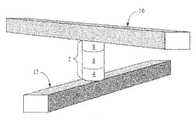
- FIG. 2illustrates a memory cell 2 formed according to a preferred embodiment of the present invention.
- a bottom conductor 12is formed of a conductive material, for example tungsten, and extends in a first direction. Barrier and adhesion layers may be included in bottom conductor 12 .
- the memory cell 2contains a polycrystalline semiconductor diode 4 .
- the diode 4preferably has a bottom heavily doped n-type region; an intrinsic region, which is not intentionally doped; and a top heavily doped p-type region, though the orientation of this diode may be reversed. Such a diode, regardless of its orientation, will be referred to as a p-i-n diode.
- the memory cellalso contains one or more conductive “decoupler” layers 6 , and an amorphous and/or polycrystalline semiconductor resistor 8 .
- the order of elements in cell 2may be reversed, and the resistor 8 may be located on the bottom of the cell and the diode 4 may be located on the top of the cell.
- the cell 2may be positioned horizontally instead of vertically with respect to the substrate.
- Top conductor 16may be formed in the same manner and of the same materials as bottom conductor 12 , and extends in a second direction different from the first direction.
- Polycrystalline semiconductor diode 4is vertically disposed between bottom conductor 12 and top conductor 16 .
- Polycrystalline semiconductor diode 4is preferably formed in a low-resistivity state.
- the resistor 8is preferably, but not necessarily formed in a high-resistivity state.
- This memory cellcan be formed above a suitable substrate, for example above a monocrystalline silicon wafer.
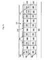
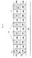
- FIG. 3shows a portion of a memory level of such devices formed in a cross-point array, where cells 2 are disposed between bottom conductors 12 and top conductors 16 .
- the diode and the resistorpreferably have a substantially cylindrical shape. Multiple memory levels can be stacked over a substrate to form a highly dense monolithic three dimensional memory array.
- the memory cell 2does not include any additional active devices, such as a transistor or a capacitor.
- the memory cell 2may contain an optional passive device, such as a fuse, an antifuse, a charge storage material, or a phase change material.
- the memory cellmay also contain an insulating material which surrounds the diode and the resistor, as will be described below, and other optional layers.
- an intrinsic regionmay in fact include a low concentration of p-type or n-type dopants. Dopants may diffuse into the intrinsic region from adjacent regions, or may be present in the deposition chamber during deposition due to contamination from an earlier deposition. It will further be understood that deposited intrinsic semiconductor material (such as silicon) may include defects which cause it to behave as if slightly n-doped. Use of the term “intrinsic” to describe silicon, germanium, a silicon-germanium alloy, or some other semiconductor material is not meant to imply that this region contains no dopants whatsoever, nor that such a region is perfectly electrically neutral.
- the memory cellcomprises a read/write memory cell, such as a rewritable memory cell.
- the resistor 8acts as the read/write element of the memory cell, by switching from a first resistivity state to a second resistivity state different from the first resistivity state in response to an applied bias (i.e., pulse) as will be explained in more detail below.
- transition from a higher resistivity, unprogrammed state to a lower resistivity, programmed statewill be called a set transition, affected by a set current, a set voltage, or a set pulse; while the reverse transition, from a lower resistivity, programmed state to a higher resistivity, unprogrammed state, will be called a reset transition, affected by a reset current, a reset voltage, or a reset pulse.
- the higher resistivity, unprogrammed statecorresponds to a “1” memory state
- the lower resistivity, programmed statecorresponds to a “0” memory state.
- the resistivity of doped polycrystalline or microcrystalline semiconductor materialcan be changed between stable states by applying appropriate electrical pulses.
- a set pulse applied with the diode under forward biaswhich is sufficient to switch the resistor's semiconductor material from a given resistivity state to a lower resistivity state will have a lower voltage amplitude than a corresponding reset pulse (which will switch the same semiconductor material from the lower resistivity state to a higher resistivity state) and will have a longer pulse width than the reset pulse.
- either set or reset of the semiconductor material making up the resistorcan be achieved without also switching the resistivity state of the diode.
- the currentflows in the forward direction through the diode 4 (i.e., a forward bias is applied) for both the set and reset transitions of the resistor 8 .
- One or more conventional driver circuits connected to the electrodes 12 , 16may be used to apply electrical pulse(s) to the read/write switching resistor element 8 for programming and reading the memory cell 2 .
- the read/write switching resistor element 8 of the memory cell 2switches from a first resistivity state to a second resistivity state different from the first resistivity state in response to an applied electrical pulse.
- an application of a second electrical pulsecan switch the read/write switching resistor element 8 from the second resistivity state back to the first resistivity state and/or to a third resistivity state different from the first and second resistivity states.
- the diode steering element 4does not switch from the first resistivity state to the second resistivity state in response to the first applied electrical pulse.
- the diode steering element 4may be formed in a low resistivity state which does not change in response to the applied electrical pulse while the read/write switching resistor element 8 is formed in a high resistivity state which changes in response to the applied electrical pulse.
- the memory cellincludes a metal silicide layer, such as titanium silicide, titanium germanide or titanium silicide-germanide layer, having the C49 phase, in physical contact with the diode 4 .
- the silicide layeracts as a crystallization template for the semiconductor diode 4 such that the diode is fabricated in the low resistivity state.
- the low resistivity of the diodeis believed to be a result of a large grain size of the polycrystalline semiconductor material that is crystallized in contact with the crystallization template.
- the resistor 8is preferably not formed in contact with a silicide template and is formed in a relatively high resistivity state.
- the resistor 8can be switched to a lower resistivity state by an application of the forward bias across the diode and the resistor arranged in series.
- distinct data states of the memory cell of the embodiments of the present inventioncorrespond to resistivity states of polycrystalline or microcrystalline semiconductor material making up the resistor, which are distinguished by detecting current flow through the memory cell (between top conductor 16 and bottom conductor 12 ) when a read voltage is applied.
- there is at least a factor of two difference between the read current flowing in any one distinct data state and any different distinct data statesuch that the difference between the states is readily detectable.
- the read current through the memory cellis higher in the lower resistivity resistor set state than in the higher resistivity resistor reset state.
- the memory cellcan be used as a one-time programmable cell or a rewriteable memory cell, and may have two, three, four, or more distinct data states.
- the cellcan be converted from any of its data states to any other of its data states in any order. Examples of writing, reading and erasing memory cells is provided in U.S. application Ser. No. 11/496,986 filed on Jul. 31, 2006, which is a continuation-in part of U.S. application Ser. No. 11/237,167, filed on Sep. 28, 2005 and in U.S. application Ser. No. 11/693,845, filed on Mar. 30, 2007, and all of which are hereby incorporated by reference in their entirety.
- this discussionhas described applying an appropriate electrical pulse to switch the semiconductor material of a resistor from one resistivity state to a different resistivity state, thus switching the memory cell between two distinct data states.
- these set and reset stepsmay be iterative processes.
- the difference between current flow during read in adjacent data statesis preferably at least a factor of two; in many embodiments, it may be preferred to establish current ranges for each data state which are separated by a factor of three, five, ten, or more. In some instances, however, it may be that after application of the electrical pulse, the read current is not in the desired range; i.e. the resistivity state of the semiconductor material of the resistor is higher or lower than intended.
- the memory cellmay be read to determine if the desired data state was reached. If the desired data state was not reached, an additional pulse is applied.
- the additional pulse or pulsesmay have a higher or lower amplitude (voltage or current) or longer or shorter pulse width than the original pulse.
- set or reset pulsesare applied as appropriate until the read current is in the desired range.
- a two-terminal devicesuch as the memory cell including a diode and resistor, it may be advantageous to read in order to verify the set or reset and to adjust if necessary.
- a single memory levelwill be described in detail. Additional memory levels can be stacked, each monolithically formed above the one below it.
- a polycrystalline and/or amorphous semiconductor resistorwill serve as the switchable memory element and the diode will serve as the steering element.
- This substrate 100can be any semiconducting substrate as known in the art, such as monocrystalline silicon, IV-IV compounds such as silicon-germanium or silicon-germanium-carbon, III-V compounds, II-VII compounds, epitaxial layers over such substrates, or any other semiconducting or non-semiconducting material.
- the substratemay include integrated circuits fabricated therein.
- the insulating layer 102is formed over substrate 100 .
- the insulating layer 102can be silicon oxide, silicon nitride, high-dielectric film, Si—C—O—H film, or any other suitable insulating material.
- the first conductors 200are formed over the substrate and insulator.
- An adhesion layer 104may be included between the insulating layer 102 and the conducting layer 106 to help conducting layer 106 adhere to insulating layer 102 . If the overlying conducting layer is tungsten, titanium nitride is preferred as adhesion layer 104 .
- Conducting layer 106can comprise any conducting material known in the art, such as tungsten, or other materials, including tantalum, titanium, copper, cobalt, or alloys thereof.
- the layerswill be patterned and etched using any suitable masking and etching process to form substantially parallel, substantially coplanar conductors 200 , shown in FIG. 4 a in cross-section.
- photoresistis deposited, patterned by photolithography and the layers etched, and then the photoresist removed using standard process techniques.
- Conductors 200could be formed by a Damascene method instead.
- Dielectric material 108is deposited over and between conductor rails 200 .
- Dielectric material 108can be any known electrically insulating material, such as silicon oxide, silicon nitride, or silicon oxynitride. In a preferred embodiment, silicon dioxide is used as dielectric material 108 .
- FIG. 4 aThis removal of dielectric overfill to form planar surface 109 can be performed by any process known in the art, such as chemical mechanical planarization (CMP) or etchback.
- CMPchemical mechanical planarization
- An etchback technique that may advantageously be usedis described in Raghuram et al., U.S. application Ser. No. 10/883,417, “Nonselective Unpatterned Etchback to Expose Buried Patterned Features,” filed Jun. 30, 2004 and hereby incorporated by reference.
- a plurality of substantially parallel first conductorshave been formed at a first height above substrate 100 .
- a barrier layer 110is deposited as the first layer after planarization of the conductor rails.
- Any suitable materialcan be used in the barrier layer, including tungsten nitride, tantalum nitride, titanium nitride, or combinations of these materials.
- titanium nitrideis used as the barrier layer.
- the barrier layeris titanium nitride, it can be deposited in the same manner as the adhesion layer described earlier.
- the semiconductor materialcan be silicon, germanium, a silicon-germanium alloy, or other suitable semiconductors, or semiconductor alloys.
- the semiconductor materialis deposited in a relatively highly resistive amorphous or polycrystalline (which includes microcrystalline) state.
- the pillarcomprises a semiconductor junction diode.
- junction diodeis used herein to refer to a semiconductor device with the property of non-ohmic conduction, having two terminal electrodes, and made of semiconducting material which is p-type at one electrode and n-type at the other. Examples include p-n diodes and n-p diodes, which have p-type semiconductor material and n-type semiconductor material in contact, such as Zener diodes, and p-i-n diodes, in which intrinsic (undoped) semiconductor material is interposed between p-type semiconductor material and n-type semiconductor material.
- Bottom heavily doped region 112can be formed by any deposition and doping method known in the art.
- the siliconcan be deposited and then doped, but is preferably doped in situ by flowing a donor gas providing n-type dopant atoms, for example phosphorus, during deposition of the silicon.
- Heavily doped region 112is preferably between about 10 and about 80 nm thick.
- Intrinsic layer 114can be formed by any method known in the art.
- Layer 114can be silicon, germanium, or any alloy of silicon or germanium and has a thickness between about 110 and about 330 nm, preferably about 200 nm.
- Pillars 300should have about the same pitch and about the same width as conductors 200 below, such that each pillar 300 is formed on top of a conductor 200 . Some misalignment can be tolerated. As will be described in more detail below, the pillar 300 patterning and etching steps may also be delayed until further in the device fabrication process.
- the pillars 300can be formed using any suitable masking and etching process.
- photoresistcan be deposited, patterned using standard photolithography techniques, and etched, then the photoresist removed.
- a hard mask of some other materialfor example silicon dioxide, can be formed on top of the semiconductor layer stack, with bottom antireflective coating (BARC) on top, then patterned and etched.
- BARCbottom antireflective coating
- DARCdielectric antireflective coating
- the pitch and width of the pillars 300can be varied as desired.
- the pitch of the pillars(the distance from the center of one pillar to the center of the next pillar) is about 300 nm, while the width of a pillar varies between about 100 and about 150 nm.
- the pitch of the pillarsis about 260 nm, while the width of a pillar varies between about 90 and 130 nm.
- the pillarspreferably have a substantially cylindrical shape with a circular or roughly circular cross section having a diameter of 250 nm or less.
- a “substantially cylindrical” elementis one with a cross section which is roughly circular; more specifically, a cross section in which no portion of the perimeter is a straight edge for a length longer than fifty percent of the longest dimension measured through the centroid of the cross-sectional area.
- a straight edgewill not be “straight” to a molecular level, and may have minute irregularities; what is relevant is the degree of rounding, as described in U.S. Pat. No. 6,952,030, incorporated herein by reference.
- Dielectric material 108is deposited over and between the semiconductor pillars 300 , filling the gaps between them.
- Dielectric material 108can be any known electrically insulating material, such as silicon oxide, silicon nitride, or silicon oxynitride. In a preferred embodiment, silicon dioxide is used as the insulating material.
- the dielectric material on top of the pillars 300is removed, exposing the tops of pillars 300 separated by dielectric material 108 , and leaving a substantially planar surface.
- This removal of dielectric overfillcan be performed by any process known in the art, such as CMP or etchback.
- the insulating layer 108is planarized such that it surrounds the semiconductor region of the pillar 300 .
- ion implantationis performed, forming heavily doped p-type top region 116 .
- the p-type dopantis preferably boron or BF 2 .
- This implant stepcompletes formation of diodes 111 , as shown in FIG. 4 b (the same diodes are numbered “ 4 ” in FIG. 2 ).
- region 116may be deposited as a layer on layer 114 before the pillar patterning step rather than being implanted into layer 114 .
- the resulting structure shown in FIG. 4 bis also shown schematically in FIG. 5 a.
- FIGS. 5 b to 5 dillustrate other permutations of diode structures.
- bottom region 112is N+ (heavily doped n-type silicon), and top region 116 is P+.
- top region 116is P+.
- bottom region 112is P+ and top region 116 is N+.
- middle region 114is N ⁇ , while in FIGS. 5 b and 5 d , middle region 114 is P ⁇ .
- the middle regioncan intentionally be lightly doped, or it can be intrinsic, or not intentionally doped.
- An undoped regionwill never be perfectly electrically neutral, and will always have defects or contaminants that cause it to behave as if slightly n-doped or p-doped.
- Such a diodecan be considered a p-i-n diode.
- a P+/N ⁇ /N+, P+/P ⁇ /N+, N+/N ⁇ /P+ or N+/P ⁇ /P+ diodecan be formed.
- an optional insulating oxide, nitride, or oxynitride layer 118may be formed on heavily doped regions 116 .
- Layer 118will be reduced during formation of a titanium silicide layer 124 (but generally not other metal silicide layers), as will be described below.
- layer 118may be omitted.
- the optional silicon dioxide layer 118is grown by oxidizing silicon at the tops of heavily doped regions 116 at about 600 to about 850° C. for about 20 seconds to about two minutes, forming between about 1 and about 5 nm of silicon dioxide.
- oxide layer 118is formed by exposing the wafer to about 800 degrees for about one minute in an oxygen-containing ambient. Layer 118 could be deposited instead.
- a layer 120 of a silicide-forming metalis deposited.
- Preferred silicide-forming metals to be used for this purposeinclude titanium or cobalt. This example will describe the use of titanium for layer 120 , but it will be understood that other materials can be used.
- Titanium layer 120is deposited to any suitable thickness, for example between about 1 and about 20 nm, preferably between about 10 and about 15 nm, most preferably about 10 nm.
- titanium nitride layer 122is deposited, preferably about 30 nm thick. Layers 120 and 122 can be deposited by any conventional method, for example by sputtering.
- An annealis performed between about 600 and about 800° C. from about 10 seconds to about two minutes, preferably between about 650 degrees and about 750 degrees, most preferably at about 670 degrees for about 20 seconds, for example in nitrogen.
- the annealserves to reduce oxide layer 118 and to react titanium layer 120 with heavily doped regions 116 where it overlies them to form titanium silicide.
- Oxide layer 118is substantially entirely reduced between titanium layer 120 and the silicon of heavily doped region 116 . If oxide layer 118 was deposited rather than grown, the rest of oxide layer 118 (between the tops of semiconductor pillars 300 , overlying dielectric fill 108 ) would remain.
- titanium nitride layer 122 and unreacted titaniumcan stripped in a selective wet etch, leaving behind titanium silicide layers 124 , each formed in a disk-shaped region on the top of one of the junction diodes, shown in FIG. 4 d .
- one or more decoupler conductive layers 6shown in FIG. 2 ), such as a new titanium nitride layer are deposited on the silicide layer 124 .
- the unreacted titanium layer 120 portions and the titanium nitride cap layer 122are not removed after the silicide layer 124 formation, but are left in the device to act as the decoupler conductive layers 6 .
- the titanium silicide feature 124 that is formed during the annealcomprises C49 phase titanium silicide.
- the C49 phasecan be obtained if the annealing temperature is maintained below 700 degrees C. for large or small sized silicon features or if the annealing temperature is maintained above 700 degrees C., but the silicon feature size is 0.25 microns or less.
- the diameter of the diodeis preferably 0.25 microns or less to form the C49 phase of titanium silicide for annealing temperature above 700 degrees C. This phase is desired due to its lattice match with amorphous silicon during the crystallization process.
- the titanium silicideIn contrast larger features (greater than a dimensional size of 0.25 microns) will allow the titanium silicide to end as the C54 phase of titanium silicide during subsequent annealing above 700 degrees C. Even though the C54 phase provides low resistivity (which is highly desired by integrated circuit manufactures), it does not provide as good a lattice match during the crystallization process of the amorphous or polycrystalline silicon. Thus, the C49 phase titanium silicide allows for the greatest enhancement to grain growth and thus a lower diode resistivity by acting as a crystallization template for the semiconductor material of the diode.
- titanium silicide layer 124could instead be some other silicide, such as cobalt silicide.
- the junction diodeis amorphous silicon as deposited, and is crystallized to form large grain, low resistivity polysilicon in contact with a silicide layer 124 .
- the crystallizationcan occur during the formation of the silicide 124 and/or during a separate crystallization anneal after the memory cell is completed.
- the separate crystallization annealmay be conducted at a temperature above about 600° C., such as 650 to 850° C. for 1 or more minutes, such as 2 minutes to 24 hours, depending on the desired degree of crystallization. A lower temperature may be used for germanium and silicon germanium diode materials.
- the silicide layer 124is advantageous for reducing the impedance of the junction diode, but may not be desired in the finished device. In an alternative embodiment, following formation of the silicide layer on the junction diode, the silicide layer can be removed.
- the semiconductor material that will be patterned into the resistor 8is deposited on the conductive layer(s).
- the semiconductor material layer that will be patterned into the resistor 8may be about 10 nm to about 40 nm thick, for example about 20 nm thick.
- the semiconductor materialcan be silicon, germanium, a silicon-germanium alloy, or other suitable semiconductors, or semiconductor alloys. For simplicity, this description will refer to the semiconductor material as silicon, but it will be understood that the skilled practitioner may select any of these other suitable materials instead.
- the semiconductor materialis deposited in a relatively highly resistive amorphous or polycrystalline (which includes microcrystalline) state.
- the semiconductor materialis deposited onto the conductive material, such as titanium nitride 122 , which does not function as a crystallization template. Therefore, during the crystallization anneal, the diode 4 which is in contact with the crystallization template material 124 , is crystallized into a lower resistivity, larger grain size state than the resistor 8 which is not in contact with the crystallization template material 124 .
- the resistor 8 materialis preferably but not necessarily an intrinsic (undoped) semiconductor material or a lightly doped semiconductor material (having a p or n-type dopant concentration below 1 ⁇ 10 17 cm ⁇ 3 ). If the resistor material is lightly doped, then it can be formed by any deposition and doping method known in the art.
- the siliconcan be deposited and then doped, but is preferably doped in situ by flowing a donor gas providing p or n-type dopant atoms, for example boron or phosphorus, during deposition of the silicon.
- the decoupler 6 and/or resistor 8 layersare then patterned to form the upper portion of the pillar 300 .
- the patterningmay comprise a separate photolithography and etching steps from those used to pattern of the diode 4 into the lower portion of the pillar 300 described above.
- the decoupler 6 and resistor 8 layersmay be patterned during the same photolithography and etching steps as the diode 4 layers to form the pillar 300 in one patterning step.
- the pillar 300 photolithography and etching stepsare delayed until the resistor 8 layer is deposited.
- the formation and planarization of the dielectric material 108is performed after the pillar 300 formation.
- the silicidation step used to form the silicide 124 and/or the diode crystallization annealing stepmay be delayed until after the entire pillar 300 , including the resistor 8 portion, is patterned.
- the titanium nitride layer 122acts as both a capping layer for silicide layer 124 formation and as a decoupler layer 6 located between the diode 4 and resistor 8 .
- FIG. 6illustrates a completed memory cell.
- Top conductors 400i.e., the upper electrode 16 shown in FIG. 2
- Conductive layer 422 and adhesion layer 420are then patterned and etched using any suitable masking and etching technique to form substantially parallel, substantially coplanar conductors 400 , shown in FIG. 6 extending perpendicular to conductors 200 .
- photoresistis deposited, patterned by photolithography and the layers etched, and then the photoresist removed using standard process techniques.
- the adhesion layer 420may be patterned together with the pillars 300 and may be located only on the pillars 300 , while the conductive layer 422 comprises a rail that contacts each portion of the adhesion layer 420 on each pillar 300 .
- the dielectric materialcan be any known electrically insulating material, such as silicon oxide, silicon nitride, or silicon oxynitride. In a preferred embodiment, silicon oxide is used as this dielectric material.
- Formation of a first memory levelhas been described. Additional memory levels can be formed above this first memory level to form a monolithic three dimensional memory array.
- conductorscan be shared between memory levels; i.e. top conductor 400 would serve as the bottom conductor of the next memory level.
- an interlevel dielectric(not shown) is formed above the first memory level of FIG. 6 , its surface planarized, and construction of a second memory level begins on this planarized interlevel dielectric, with no shared conductors.
- a monolithic three dimensional memory arrayis one in which multiple memory levels are formed above a single substrate, such as a wafer, with no intervening substrates.
- the layers forming one memory levelare deposited or grown directly over the layers of an existing level or levels.
- stacked memorieshave been constructed by forming memory levels on separate substrates and adhering the memory levels atop each other, as in Leedy, U.S. Pat. No. 5,915,167, “Three dimensional structure memory.”
- the substratesmay be thinned or removed from the memory levels before bonding, but as the memory levels are initially formed over separate substrates, such memories are not true monolithic three dimensional memory arrays.
- Monolithic three dimensional memory arraysare described in Johnson et al., U.S. Pat. No. 6,034,882, “Vertically stacked field programmable nonvolatile memory and method of fabrication”; Johnson, U.S. Pat. No. 6,525,953, “Vertically stacked field programmable nonvolatile memory and method of fabrication”; Knall et al., U.S. Pat. No. 6,420,215, “Three Dimensional Memory Array and Method of Fabrication”; Herner, U.S. application Ser. No. 10/095,962, “Silicide-Silicon Oxide-Semiconductor Antifuse Device and Method of Making,” filed Mar.
- One embodiment of the present inventionhas been described herein in the context of a monolithic three dimensional memory array formed above a substrate.
- Such an arraycomprises at least a first memory level formed at a first height above the substrate and a second memory level formed at a second height different from the first height.
- Three, four, eight, or more memory levelscan be formed above the substrate in such a multilevel array.
- Each memory levelis monolithically formed on the memory level below it.
- the memory cell formed in a monolithic three dimensional memory arrayhas stacked memory levels, but such cells could clearly be formed in a two-dimensional array, as well.
- the example givenshowed the silicide layer formed above the junction diode, but those skilled in the art will appreciate that the silicide layer can be formed elsewhere: beside the junction diode or below it, for example. Many configurations can be imagined.
- the resistor 8is formed below the diode 4 in the pillar 300 .
- the resistor 8is formed on the lower electrode 12 .
- the decoupler conductive layer 6is formed on the resistor 4 .
- the diode 4is then formed on the decoupler layer 6 .
- the silicide crystallization template layer 124may be formed in the contact with the diode either above or below the diode 4 .
Landscapes
- Semiconductor Memories (AREA)
Abstract
Description
- This application is related to Kumar et al., U.S. application Ser. No. ______, titled “3D R/W CELL WITH REDUCED REVERSE LEAKAGE” (Attorney Docket No. 035905/0162), filed on the same day herewith, and hereby incorporated by reference in its entirety.
- The invention relates to a nonvolatile memory device and a method of making the device.
- Nonvolatile memory arrays maintain their data even when power to the device is turned off. In one-time-programmable arrays, each memory cell is formed in an initial unprogrammed state, and can be converted to a programmed state. This change is permanent, and such cells are not erasable. In other types of memories, the memory cells are erasable, and can be rewritten many times.
- Cells may also vary in the number of data states each cell can achieve. A data state may be stored by altering some characteristic of the cell which can be detected, such as current flowing through the cell under a given applied voltage or the threshold voltage of a transistor within the cell. A data state is a distinct value of the cell, such as a data ‘0’ or a data ‘1’.
- Some solutions for achieving erasable or multi-state cells are complex. Floating gate and SONOS memory cells, for example, operate by storing charge, where the presence, absence or amount of stored charge changes a transistor threshold voltage. These memory cells are three-terminal devices which are relatively difficult to fabricate and operate at the very small dimensions required for competitiveness in modern integrated circuits.
- Other memory cells operate by changing the resistivity of relatively exotic materials, like chalcogenides. Chalcogenides are difficult to work with and can present challenges in most semiconductor production facilities.
- A substantial advantage would be provided by a nonvolatile memory array having erasable or multi-state memory cells formed using conventional semiconductor materials in structures that are readily scaled to small size.
- One embodiment of the invention provides a method of making a nonvolatile memory device, comprising forming a semiconductor diode steering element, and forming a semiconductor read/write switching element.
- Another embodiment of the invention provides a method of making a nonvolatile memory device, comprising forming a semiconductor diode steering element, forming a semiconductor resistor read/write switching element, forming at least one conductive layer located between the steering element and the read/write switching element, forming a first electrode electrically contacting the steering element, and forming a second electrode electrically contacting the read/write switching element. The read/write switching element, the at least one conductive layer and the steering element are arranged in series in a pillar between the first electrode and the second electrode.
- Another embodiment of the invention provides a method of operating a nonvolatile memory device, comprising providing a non-volatile memory cell comprising a semiconductor diode steering element, a semiconductor read/write switching element, and at least one conductive layer located between the steering element and the read/write switching element, first switching the read/write switching element from a first resistivity state to a second resistivity state different from the first resistivity state, and second switching the read/write switching element from the second resistivity state to the first resistivity state.
- Each of the aspects and embodiments of the invention described herein can be used alone or in combination with one another. The preferred aspects and embodiments will now be described with reference to the attached drawings.
FIG. 1 is a circuit diagram illustrating the need for electrical isolation between memory cells in a memory array.FIGS. 2 and 6 are perspective views of memory cells formed according to a preferred embodiment of the present invention.FIG. 3 is a perspective view of a portion of a memory level comprising the memory cells ofFIG. 2 .FIGS. 4 a-4dare side cross-sectional views illustrating stages in formation of a memory level formed according to an embodiment of the present invention.FIGS. 5 a-5dare schematic side cross-sectional views illustrating alternative diode configurations according to an embodiment of the present invention.- It has been known that by applying electrical pulses, the resistance of a resistor formed of doped polycrystalline silicon, or polysilicon, can be trimmed, adjusting it between stable resistance states. Such trimmable resistors have been used as elements in integrated circuits.
- However, trimmable polysilicon resistors are not conventionally used to store a data state in a nonvolatile memory cell. Making a memory array of polysilicon resistors presents difficulties. If resistors are used as memory cells in a large cross-point array, when voltage is applied to a selected cell, there will be undesired leakage through half-selected and unselected cells throughout the array. For example, turning to
FIG. 1 , suppose a voltage is applied between bitline B and wordline A to set, reset, or sense selected cell S. Current is intended to flow through selected cell S. Some leakage current, however, may flow on alternate paths, for example between bitline B and wordline A through unselected cells U1, U2, and U3. Many such alternate paths may exist. - In one embodiment of the invention, the leakage current can be greatly reduced by forming each memory cell as a two-terminal device including a diode and a resistor. A diode has a non-linear I-V characteristic, allowing very little current flow below a turn-on voltage, and substantially higher current flow above the turn-on voltage. In general, a diode also acts as one-way valve passing current more easily in one direction than the other. Thus, so long as biasing schemes are selected that assure that only the selected cell is subjected to a forward current above the turn-on voltage, leakage current along unintended paths (such as the U1-U2-U3 sneak path of
FIG. 1 ) can be greatly reduced. - In embodiments of the present invention, by applying appropriate electrical pulses, a memory element formed of semiconductor material, for example a diode steering element and a semiconductor resistor which functions as a read/write switching element, can achieve two or more stable resistivity states. The switching element is located in series, but preferably decoupled from the diode steering element. Preferably, the switching element is decoupled from the steering element by one or more conductive layers, such as metal (Ti, W, etc.), metal silicide or titanium nitride layers, which are located between the switching and steering elements. The switching element, the steering element and the conductive decoupling layer are arranged in series form a non-volatile memory cell. The switching element preferably comprises amorphous, polycrystalline or a combination amorphous and polycrystalline Group IV semiconductor resistor. However, other switching elements, such as high resistivity diodes can also be used. The steering element preferably comprises a crystallized, low resistivity polycrystalline Group IV semiconductor diode.
- The semiconductor resistor material can be converted from an initial first resistivity state to a different resistivity state; then, upon application of an appropriate electrical pulse, can be returned to the first resistivity state. For example, the first state may be a higher resistivity state than the second state. Alternatively, the second state may be a lower state than the first resistivity state. The memory cell can have two or more data states, and can be one-time-programmable or rewriteable.
- As noted, including a diode between conductors in the memory cell allows its formation in a highly dense cross-point memory array. In preferred embodiments of the present invention, then, a polycrystalline and/or amorphous semiconductor memory element is formed of the decoupled diode and the resistor in series.
FIG. 2 illustrates amemory cell 2 formed according to a preferred embodiment of the present invention. Abottom conductor 12 is formed of a conductive material, for example tungsten, and extends in a first direction. Barrier and adhesion layers may be included inbottom conductor 12. Thememory cell 2 contains apolycrystalline semiconductor diode 4. Thediode 4 preferably has a bottom heavily doped n-type region; an intrinsic region, which is not intentionally doped; and a top heavily doped p-type region, though the orientation of this diode may be reversed. Such a diode, regardless of its orientation, will be referred to as a p-i-n diode. The memory cell also contains one or more conductive “decoupler”layers 6, and an amorphous and/orpolycrystalline semiconductor resistor 8. The order of elements incell 2 may be reversed, and theresistor 8 may be located on the bottom of the cell and thediode 4 may be located on the top of the cell. Furthermore, thecell 2 may be positioned horizontally instead of vertically with respect to the substrate.Top conductor 16 may be formed in the same manner and of the same materials asbottom conductor 12, and extends in a second direction different from the first direction.Polycrystalline semiconductor diode 4 is vertically disposed betweenbottom conductor 12 andtop conductor 16.Polycrystalline semiconductor diode 4 is preferably formed in a low-resistivity state. Theresistor 8 is preferably, but not necessarily formed in a high-resistivity state. This memory cell can be formed above a suitable substrate, for example above a monocrystalline silicon wafer.FIG. 3 shows a portion of a memory level of such devices formed in a cross-point array, wherecells 2 are disposed betweenbottom conductors 12 andtop conductors 16. As shown inFIGS. 2 and 3 , the diode and the resistor preferably have a substantially cylindrical shape. Multiple memory levels can be stacked over a substrate to form a highly dense monolithic three dimensional memory array.- Preferably, the
memory cell 2 does not include any additional active devices, such as a transistor or a capacitor. However, if desired, thememory cell 2 may contain an optional passive device, such as a fuse, an antifuse, a charge storage material, or a phase change material. The memory cell may also contain an insulating material which surrounds the diode and the resistor, as will be described below, and other optional layers. - In this discussion, a region of semiconductor material which is not intentionally doped is described as an intrinsic region. It will be understood by those skilled in the art, however, that an intrinsic region may in fact include a low concentration of p-type or n-type dopants. Dopants may diffuse into the intrinsic region from adjacent regions, or may be present in the deposition chamber during deposition due to contamination from an earlier deposition. It will further be understood that deposited intrinsic semiconductor material (such as silicon) may include defects which cause it to behave as if slightly n-doped. Use of the term “intrinsic” to describe silicon, germanium, a silicon-germanium alloy, or some other semiconductor material is not meant to imply that this region contains no dopants whatsoever, nor that such a region is perfectly electrically neutral.
- The memory cell comprises a read/write memory cell, such as a rewritable memory cell. The
resistor 8 acts as the read/write element of the memory cell, by switching from a first resistivity state to a second resistivity state different from the first resistivity state in response to an applied bias (i.e., pulse) as will be explained in more detail below. - In this discussion, transition from a higher resistivity, unprogrammed state to a lower resistivity, programmed state will be called a set transition, affected by a set current, a set voltage, or a set pulse; while the reverse transition, from a lower resistivity, programmed state to a higher resistivity, unprogrammed state, will be called a reset transition, affected by a reset current, a reset voltage, or a reset pulse. The higher resistivity, unprogrammed state corresponds to a “1” memory state, while the lower resistivity, programmed state corresponds to a “0” memory state.
- The resistivity of doped polycrystalline or microcrystalline semiconductor material, for example silicon, can be changed between stable states by applying appropriate electrical pulses. Generally a set pulse applied with the diode under forward bias which is sufficient to switch the resistor's semiconductor material from a given resistivity state to a lower resistivity state will have a lower voltage amplitude than a corresponding reset pulse (which will switch the same semiconductor material from the lower resistivity state to a higher resistivity state) and will have a longer pulse width than the reset pulse.
- By selecting appropriate voltages, either set or reset of the semiconductor material making up the resistor can be achieved without also switching the resistivity state of the diode. Preferably the current flows in the forward direction through the diode4 (i.e., a forward bias is applied) for both the set and reset transitions of the
resistor 8. One or more conventional driver circuits connected to theelectrodes resistor element 8 for programming and reading thememory cell 2. - Thus, in use, the read/write switching
resistor element 8 of thememory cell 2 switches from a first resistivity state to a second resistivity state different from the first resistivity state in response to an applied electrical pulse. If desired, an application of a second electrical pulse can switch the read/write switchingresistor element 8 from the second resistivity state back to the first resistivity state and/or to a third resistivity state different from the first and second resistivity states. However, thediode steering element 4 does not switch from the first resistivity state to the second resistivity state in response to the first applied electrical pulse. For example, thediode steering element 4 may be formed in a low resistivity state which does not change in response to the applied electrical pulse while the read/write switchingresistor element 8 is formed in a high resistivity state which changes in response to the applied electrical pulse. - As will be explained in more detail below, the memory cell includes a metal silicide layer, such as titanium silicide, titanium germanide or titanium silicide-germanide layer, having the C49 phase, in physical contact with the
diode 4. The silicide layer acts as a crystallization template for thesemiconductor diode 4 such that the diode is fabricated in the low resistivity state. Without wishing to be bound by a particular theory, the low resistivity of the diode is believed to be a result of a large grain size of the polycrystalline semiconductor material that is crystallized in contact with the crystallization template. It is believed that a diode formed in the low resistivity state, such as by crystallization in contact with a silicide template, will not switch to a high resistivity state in response to an application of a forward bias across the diode. In contrast, theresistor 8 is preferably not formed in contact with a silicide template and is formed in a relatively high resistivity state. Thus, theresistor 8 can be switched to a lower resistivity state by an application of the forward bias across the diode and the resistor arranged in series. - Herner et al., U.S. patent application Ser. No. 11/148,530, “Nonvolatile Memory Cell Operating by Increasing Order in Polycrystalline Semiconductor Material,” filed Jun. 8, 2006; and Herner, U.S. patent application Ser. No. 10/954,510, “Memory Cell Comprising a Semiconductor Junction Diode Crystallized Adjacent to a Silicide,” filed Sep. 29, 2004, both owned by the assignee of the present invention and both hereby incorporated by reference, describe that crystallization of polysilicon adjacent to an appropriate silicide affects the properties of the polysilicon. Certain metal silicides, such as cobalt silicide and titanium silicide, have a lattice structure very close to that of silicon. When amorphous or microcrystalline silicon is crystallized in contact with one of these silicides, the crystal lattice of the silicide provides a template to the silicon during crystallization. The resulting polysilicon will be highly ordered, and relatively low in defects. This high-quality polysilicon, when doped with a conductivity-enhancing dopant, is relatively highly conductive as formed.
- After application of the switching pulse, a smaller read pulse, for example 1.5 to 2 volts, is applied, and the current flowing through the diode and resistor at the read voltage, called the read current, is measured. As the voltage of the switching pulse is increased in subsequent pulses, the subsequent read current at a given read voltage changes. Thus, distinct data states of the memory cell of the embodiments of the present invention correspond to resistivity states of polycrystalline or microcrystalline semiconductor material making up the resistor, which are distinguished by detecting current flow through the memory cell (between
top conductor 16 and bottom conductor12) when a read voltage is applied. Preferably, there is at least a factor of two difference between the read current flowing in any one distinct data state and any different distinct data state such that the difference between the states is readily detectable. The read current through the memory cell is higher in the lower resistivity resistor set state than in the higher resistivity resistor reset state. The memory cell can be used as a one-time programmable cell or a rewriteable memory cell, and may have two, three, four, or more distinct data states. The cell can be converted from any of its data states to any other of its data states in any order. Examples of writing, reading and erasing memory cells is provided in U.S. application Ser. No. 11/496,986 filed on Jul. 31, 2006, which is a continuation-in part of U.S. application Ser. No. 11/237,167, filed on Sep. 28, 2005 and in U.S. application Ser. No. 11/693,845, filed on Mar. 30, 2007, and all of which are hereby incorporated by reference in their entirety. - So far, this discussion has described applying an appropriate electrical pulse to switch the semiconductor material of a resistor from one resistivity state to a different resistivity state, thus switching the memory cell between two distinct data states. In practice, these set and reset steps may be iterative processes. As described, the difference between current flow during read in adjacent data states is preferably at least a factor of two; in many embodiments, it may be preferred to establish current ranges for each data state which are separated by a factor of three, five, ten, or more. In some instances, however, it may be that after application of the electrical pulse, the read current is not in the desired range; i.e. the resistivity state of the semiconductor material of the resistor is higher or lower than intended. After an electrical pulse is applied to switch the memory cell to a desired data state, the memory cell may be read to determine if the desired data state was reached. If the desired data state was not reached, an additional pulse is applied. The additional pulse or pulses may have a higher or lower amplitude (voltage or current) or longer or shorter pulse width than the original pulse. After the additional set pulse, the cell is read again, then set or reset pulses are applied as appropriate until the read current is in the desired range. In a two-terminal device, such as the memory cell including a diode and resistor, it may be advantageous to read in order to verify the set or reset and to adjust if necessary.
- Fabrication of a single memory level will be described in detail. Additional memory levels can be stacked, each monolithically formed above the one below it. In this embodiment, a polycrystalline and/or amorphous semiconductor resistor will serve as the switchable memory element and the diode will serve as the steering element.
- Turning to
FIG. 4 a, formation of the memory begins with asubstrate 100. Thissubstrate 100 can be any semiconducting substrate as known in the art, such as monocrystalline silicon, IV-IV compounds such as silicon-germanium or silicon-germanium-carbon, III-V compounds, II-VII compounds, epitaxial layers over such substrates, or any other semiconducting or non-semiconducting material. The substrate may include integrated circuits fabricated therein. - An insulating
layer 102 is formed oversubstrate 100. The insulatinglayer 102 can be silicon oxide, silicon nitride, high-dielectric film, Si—C—O—H film, or any other suitable insulating material. - The first conductors200 (i.e., the
lower electrode 12 shown inFIG. 2 ) are formed over the substrate and insulator. Anadhesion layer 104 may be included between the insulatinglayer 102 and theconducting layer 106 to help conductinglayer 106 adhere to insulatinglayer 102. If the overlying conducting layer is tungsten, titanium nitride is preferred asadhesion layer 104. - The next layer to be deposited is conducting
layer 106. Conductinglayer 106 can comprise any conducting material known in the art, such as tungsten, or other materials, including tantalum, titanium, copper, cobalt, or alloys thereof. - Once all the layers that will form the conductor rails have been deposited, the layers will be patterned and etched using any suitable masking and etching process to form substantially parallel, substantially
coplanar conductors 200, shown inFIG. 4 ain cross-section. In one embodiment, photoresist is deposited, patterned by photolithography and the layers etched, and then the photoresist removed using standard process techniques.Conductors 200 could be formed by a Damascene method instead. - Next, a
dielectric material 108 is deposited over and between conductor rails200.Dielectric material 108 can be any known electrically insulating material, such as silicon oxide, silicon nitride, or silicon oxynitride. In a preferred embodiment, silicon dioxide is used asdielectric material 108. - Finally, excess
dielectric material 108 on top ofconductor rails 200 is removed, exposing the tops ofconductor rails 200 separated bydielectric material 108, and leaving a substantiallyplanar surface 109. The resulting structure is shown inFIG. 4 a. This removal of dielectric overfill to formplanar surface 109 can be performed by any process known in the art, such as chemical mechanical planarization (CMP) or etchback. An etchback technique that may advantageously be used is described in Raghuram et al., U.S. application Ser. No. 10/883,417, “Nonselective Unpatterned Etchback to Expose Buried Patterned Features,” filed Jun. 30, 2004 and hereby incorporated by reference. At this stage, a plurality of substantially parallel first conductors have been formed at a first height abovesubstrate 100. - Next, turning to
FIG. 4 b, vertical pillars will be formed above completed conductor rails200. (To savespace substrate 100 is not shown inFIG. 4 b; its presence will be assumed.) Preferably abarrier layer 110 is deposited as the first layer after planarization of the conductor rails. Any suitable material can be used in the barrier layer, including tungsten nitride, tantalum nitride, titanium nitride, or combinations of these materials. In a preferred embodiment, titanium nitride is used as the barrier layer. Where the barrier layer is titanium nitride, it can be deposited in the same manner as the adhesion layer described earlier. - Next semiconductor material that will be patterned into pillars is deposited. The semiconductor material can be silicon, germanium, a silicon-germanium alloy, or other suitable semiconductors, or semiconductor alloys. For simplicity, this description will refer to the semiconductor material as silicon, but it will be understood that the skilled practitioner may select any of these other suitable materials instead. Preferably, the semiconductor material is deposited in a relatively highly resistive amorphous or polycrystalline (which includes microcrystalline) state.
- In preferred embodiments, the pillar comprises a semiconductor junction diode. The term junction diode is used herein to refer to a semiconductor device with the property of non-ohmic conduction, having two terminal electrodes, and made of semiconducting material which is p-type at one electrode and n-type at the other. Examples include p-n diodes and n-p diodes, which have p-type semiconductor material and n-type semiconductor material in contact, such as Zener diodes, and p-i-n diodes, in which intrinsic (undoped) semiconductor material is interposed between p-type semiconductor material and n-type semiconductor material.
- Bottom heavily doped
region 112 can be formed by any deposition and doping method known in the art. The silicon can be deposited and then doped, but is preferably doped in situ by flowing a donor gas providing n-type dopant atoms, for example phosphorus, during deposition of the silicon. Heavily dopedregion 112 is preferably between about 10 and about 80 nm thick. Intrinsic layer 114 can be formed by any method known in the art.Layer 114 can be silicon, germanium, or any alloy of silicon or germanium and has a thickness between about 110 and about 330 nm, preferably about 200 nm.- Returning to
FIG. 4 b, semiconductor layers114 and112 just deposited, along withunderlying barrier layer 110, can be patterned and etched to formpillars 300.Pillars 300 should have about the same pitch and about the same width asconductors 200 below, such that eachpillar 300 is formed on top of aconductor 200. Some misalignment can be tolerated. As will be described in more detail below, thepillar 300 patterning and etching steps may also be delayed until further in the device fabrication process. - The
pillars 300 can be formed using any suitable masking and etching process. For example, photoresist can be deposited, patterned using standard photolithography techniques, and etched, then the photoresist removed. Alternatively, a hard mask of some other material, for example silicon dioxide, can be formed on top of the semiconductor layer stack, with bottom antireflective coating (BARC) on top, then patterned and etched. Similarly, dielectric antireflective coating (DARC) can be used as a hard mask. - The photolithography techniques described in Chen, U.S. application Ser. No. 10/728,436, “Photomask Features with Interior Nonprinting Window Using Alternating Phase Shifting,” filed Dec. 5, 2003; or Chen, U.S. application Ser. No. 10/815,312, Photomask Features with Chromeless Nonprinting Phase Shifting Window,” filed Apr. 1, 2004, both owned by the assignee of the present invention and hereby incorporated by reference, can advantageously be used to perform any photolithography step used in formation of a memory array according to the embodiments of the present invention.
- The pitch and width of the
pillars 300 can be varied as desired. In one preferred embodiment, the pitch of the pillars (the distance from the center of one pillar to the center of the next pillar) is about 300 nm, while the width of a pillar varies between about 100 and about 150 nm. In another preferred embodiment, the pitch of the pillars is about 260 nm, while the width of a pillar varies between about 90 and 130 nm. In general, the pillars preferably have a substantially cylindrical shape with a circular or roughly circular cross section having a diameter of 250 nm or less. A “substantially cylindrical” element is one with a cross section which is roughly circular; more specifically, a cross section in which no portion of the perimeter is a straight edge for a length longer than fifty percent of the longest dimension measured through the centroid of the cross-sectional area. Clearly, a straight edge will not be “straight” to a molecular level, and may have minute irregularities; what is relevant is the degree of rounding, as described in U.S. Pat. No. 6,952,030, incorporated herein by reference. Dielectric material 108 is deposited over and between thesemiconductor pillars 300, filling the gaps between them.Dielectric material 108 can be any known electrically insulating material, such as silicon oxide, silicon nitride, or silicon oxynitride. In a preferred embodiment, silicon dioxide is used as the insulating material.- Next the dielectric material on top of the
pillars 300 is removed, exposing the tops ofpillars 300 separated bydielectric material 108, and leaving a substantially planar surface. This removal of dielectric overfill can be performed by any process known in the art, such as CMP or etchback. The insulatinglayer 108 is planarized such that it surrounds the semiconductor region of thepillar 300. After CMP or etchback, ion implantation is performed, forming heavily doped p-type top region 116. The p-type dopant is preferably boron or BF2. This implant step completes formation ofdiodes 111, as shown inFIG. 4 b(the same diodes are numbered “4” inFIG. 2 ). Alternatively,region 116 may be deposited as a layer onlayer 114 before the pillar patterning step rather than being implanted intolayer 114. The resulting structure shown inFIG. 4 bis also shown schematically inFIG. 5 a. FIGS. 5 bto5dillustrate other permutations of diode structures. In the diodes ofFIGS. 5 aand5b,bottom region 112 is N+ (heavily doped n-type silicon), andtop region 116 is P+. In the diodes ofFIGS. 5 cand5d,bottom region 112 is P+ andtop region 116 is N+. InFIGS. 5 aand5c,middle region 114 is N−, while inFIGS. 5 band5d,middle region 114 is P−. The middle region can intentionally be lightly doped, or it can be intrinsic, or not intentionally doped. An undoped region will never be perfectly electrically neutral, and will always have defects or contaminants that cause it to behave as if slightly n-doped or p-doped. Such a diode can be considered a p-i-n diode. Thus, a P+/N−/N+, P+/P−/N+, N+/N−/P+ or N+/P−/P+ diode can be formed.- Turning to
FIG. 4 c, next an optional insulating oxide, nitride, oroxynitride layer 118 may be formed on heavily dopedregions 116.Layer 118 will be reduced during formation of a titanium silicide layer124 (but generally not other metal silicide layers), as will be described below. Alternatively,layer 118 may be omitted. For example, the optionalsilicon dioxide layer 118 is grown by oxidizing silicon at the tops of heavily dopedregions 116 at about 600 to about 850° C. for about 20 seconds to about two minutes, forming between about 1 and about 5 nm of silicon dioxide. Preferably,oxide layer 118 is formed by exposing the wafer to about 800 degrees for about one minute in an oxygen-containing ambient.Layer 118 could be deposited instead. - Next, a
layer 120 of a silicide-forming metal is deposited. Preferred silicide-forming metals to be used for this purpose include titanium or cobalt. This example will describe the use of titanium forlayer 120, but it will be understood that other materials can be used. Titanium layer 120 is deposited to any suitable thickness, for example between about 1 and about 20 nm, preferably between about 10 and about 15 nm, most preferably about 10 nm. To prevent oxidation oftitanium layer 120,titanium nitride layer 122 is deposited, preferably about 30 nm thick.Layers - An anneal is performed between about 600 and about 800° C. from about 10 seconds to about two minutes, preferably between about 650 degrees and about 750 degrees, most preferably at about 670 degrees for about 20 seconds, for example in nitrogen. The anneal serves to reduce
oxide layer 118 and to reacttitanium layer 120 with heavily dopedregions 116 where it overlies them to form titanium silicide.Oxide layer 118 is substantially entirely reduced betweentitanium layer 120 and the silicon of heavily dopedregion 116. Ifoxide layer 118 was deposited rather than grown, the rest of oxide layer118 (between the tops ofsemiconductor pillars 300, overlying dielectric fill108) would remain. - As in a conventional salicide process,
titanium nitride layer 122 and unreacted titanium can stripped in a selective wet etch, leaving behindtitanium silicide layers 124, each formed in a disk-shaped region on the top of one of the junction diodes, shown inFIG. 4 d. Thereafter, one or more decoupler conductive layers6 (shown inFIG. 2 ), such as a new titanium nitride layer are deposited on thesilicide layer 124. Alternatively, theunreacted titanium layer 120 portions and the titaniumnitride cap layer 122 are not removed after thesilicide layer 124 formation, but are left in the device to act as the decouplerconductive layers 6. - In a preferred embodiment, the
titanium silicide feature 124 that is formed during the anneal comprises C49 phase titanium silicide. The C49 phase can be obtained if the annealing temperature is maintained below 700 degrees C. for large or small sized silicon features or if the annealing temperature is maintained above 700 degrees C., but the silicon feature size is 0.25 microns or less. Thus, the diameter of the diode is preferably 0.25 microns or less to form the C49 phase of titanium silicide for annealing temperature above 700 degrees C. This phase is desired due to its lattice match with amorphous silicon during the crystallization process. In contrast larger features (greater than a dimensional size of 0.25 microns) will allow the titanium silicide to end as the C54 phase of titanium silicide during subsequent annealing above 700 degrees C. Even though the C54 phase provides low resistivity (which is highly desired by integrated circuit manufactures), it does not provide as good a lattice match during the crystallization process of the amorphous or polycrystalline silicon. Thus, the C49 phase titanium silicide allows for the greatest enhancement to grain growth and thus a lower diode resistivity by acting as a crystallization template for the semiconductor material of the diode. - As noted, in this example it is assumed that titanium is used in the silicide-forming
metal layer 120, but other materials, including cobalt, could have been used instead. Thus, thetitanium silicide layer 124 could instead be some other silicide, such as cobalt silicide. - In preferred embodiments, the junction diode is amorphous silicon as deposited, and is crystallized to form large grain, low resistivity polysilicon in contact with a
silicide layer 124. The crystallization can occur during the formation of thesilicide 124 and/or during a separate crystallization anneal after the memory cell is completed. The separate crystallization anneal may be conducted at a temperature above about 600° C., such as 650 to 850° C. for 1 or more minutes, such as 2 minutes to 24 hours, depending on the desired degree of crystallization. A lower temperature may be used for germanium and silicon germanium diode materials. Thesilicide layer 124 is advantageous for reducing the impedance of the junction diode, but may not be desired in the finished device. In an alternative embodiment, following formation of the silicide layer on the junction diode, the silicide layer can be removed. - After the formation of the one or more conductive decoupler layer(s)120,122 and/or124, the semiconductor material that will be patterned into the
resistor 8 is deposited on the conductive layer(s). The semiconductor material layer that will be patterned into theresistor 8 may be about 10 nm to about 40 nm thick, for example about 20 nm thick. The semiconductor material can be silicon, germanium, a silicon-germanium alloy, or other suitable semiconductors, or semiconductor alloys. For simplicity, this description will refer to the semiconductor material as silicon, but it will be understood that the skilled practitioner may select any of these other suitable materials instead. Preferably, the semiconductor material is deposited in a relatively highly resistive amorphous or polycrystalline (which includes microcrystalline) state. Preferably, the semiconductor material is deposited onto the conductive material, such astitanium nitride 122, which does not function as a crystallization template. Therefore, during the crystallization anneal, thediode 4 which is in contact with thecrystallization template material 124, is crystallized into a lower resistivity, larger grain size state than theresistor 8 which is not in contact with thecrystallization template material 124. - The
resistor 8 material is preferably but not necessarily an intrinsic (undoped) semiconductor material or a lightly doped semiconductor material (having a p or n-type dopant concentration below 1×1017cm−3). If the resistor material is lightly doped, then it can be formed by any deposition and doping method known in the art. The silicon can be deposited and then doped, but is preferably doped in situ by flowing a donor gas providing p or n-type dopant atoms, for example boron or phosphorus, during deposition of the silicon. - The
decoupler 6 and/orresistor 8 layers are then patterned to form the upper portion of thepillar 300. The patterning may comprise a separate photolithography and etching steps from those used to pattern of thediode 4 into the lower portion of thepillar 300 described above. - In an alternative embodiment, the
decoupler 6 andresistor 8 layers may be patterned during the same photolithography and etching steps as thediode 4 layers to form thepillar 300 in one patterning step. In this embodiment, thepillar 300 photolithography and etching steps are delayed until theresistor 8 layer is deposited. The formation and planarization of thedielectric material 108 is performed after thepillar 300 formation. If desired, the silicidation step used to form thesilicide 124 and/or the diode crystallization annealing step may be delayed until after theentire pillar 300, including theresistor 8 portion, is patterned. In this case, thetitanium nitride layer 122 acts as both a capping layer forsilicide layer 124 formation and as adecoupler layer 6 located between thediode 4 andresistor 8. FIG. 6 illustrates a completed memory cell. Top conductors400 (i.e., theupper electrode 16 shown inFIG. 2 ) can be formed in the same manner asbottom conductors 200, for example by depositingadhesion layer 420, preferably of titanium nitride, andconductive layer 422, preferably of tungsten.Conductive layer 422 andadhesion layer 420 are then patterned and etched using any suitable masking and etching technique to form substantially parallel, substantiallycoplanar conductors 400, shown inFIG. 6 extending perpendicular toconductors 200. In a preferred embodiment, photoresist is deposited, patterned by photolithography and the layers etched, and then the photoresist removed using standard process techniques. If desired, theadhesion layer 420 may be patterned together with thepillars 300 and may be located only on thepillars 300, while theconductive layer 422 comprises a rail that contacts each portion of theadhesion layer 420 on eachpillar 300.- Next a dielectric material (not shown) is deposited over and between conductor rails400. The dielectric material can be any known electrically insulating material, such as silicon oxide, silicon nitride, or silicon oxynitride. In a preferred embodiment, silicon oxide is used as this dielectric material.
- Formation of a first memory level has been described. Additional memory levels can be formed above this first memory level to form a monolithic three dimensional memory array. In some embodiments, conductors can be shared between memory levels; i.e.
top conductor 400 would serve as the bottom conductor of the next memory level. In other embodiments, an interlevel dielectric (not shown) is formed above the first memory level ofFIG. 6 , its surface planarized, and construction of a second memory level begins on this planarized interlevel dielectric, with no shared conductors. - A monolithic three dimensional memory array is one in which multiple memory levels are formed above a single substrate, such as a wafer, with no intervening substrates. The layers forming one memory level are deposited or grown directly over the layers of an existing level or levels. In contrast, stacked memories have been constructed by forming memory levels on separate substrates and adhering the memory levels atop each other, as in Leedy, U.S. Pat. No. 5,915,167, “Three dimensional structure memory.” The substrates may be thinned or removed from the memory levels before bonding, but as the memory levels are initially formed over separate substrates, such memories are not true monolithic three dimensional memory arrays.
- Monolithic three dimensional memory arrays are described in Johnson et al., U.S. Pat. No. 6,034,882, “Vertically stacked field programmable nonvolatile memory and method of fabrication”; Johnson, U.S. Pat. No. 6,525,953, “Vertically stacked field programmable nonvolatile memory and method of fabrication”; Knall et al., U.S. Pat. No. 6,420,215, “Three Dimensional Memory Array and Method of Fabrication”; Herner, U.S. application Ser. No. 10/095,962, “Silicide-Silicon Oxide-Semiconductor Antifuse Device and Method of Making,” filed Mar. 13, 2002; Vyvoda et al., U.S. patent application Ser. No. 10/185,507, “Electrically Isolated Pillars in Active Devices,” filed Jun. 27, 2002; Vyvoda, U.S. patent application Ser. No. 10/440,882, “Rail Schottky Device and Method of Making”, filed May 19, 2003; and Cleeves et al., “Optimization of Critical Dimensions and Pitch of Patterned Features in and Above a Substrate,” U.S. patent application Ser. No. 10/728,451, filed Dec. 5, 2003, all assigned to the assignee of the present invention and hereby incorporated by reference.
- One embodiment of the present invention has been described herein in the context of a monolithic three dimensional memory array formed above a substrate. Such an array comprises at least a first memory level formed at a first height above the substrate and a second memory level formed at a second height different from the first height. Three, four, eight, or more memory levels can be formed above the substrate in such a multilevel array. Each memory level is monolithically formed on the memory level below it.
- The memory cell formed in a monolithic three dimensional memory array has stacked memory levels, but such cells could clearly be formed in a two-dimensional array, as well. The example given showed the silicide layer formed above the junction diode, but those skilled in the art will appreciate that the silicide layer can be formed elsewhere: beside the junction diode or below it, for example. Many configurations can be imagined.
- In an alternative embodiment, the
resistor 8 is formed below thediode 4 in thepillar 300. In this embodiment, theresistor 8 is formed on thelower electrode 12. The decouplerconductive layer 6 is formed on theresistor 4. Thediode 4 is then formed on thedecoupler layer 6. The silicidecrystallization template layer 124 may be formed in the contact with the diode either above or below thediode 4. - An alternative method for forming a similar array in which conductors are formed using Damascene construction is described in Radigan et al., U.S. patent application Ser. No. 11/444,936, “Conductive Hard Mask to Protect Patterned Features During Trench Etch,” filed May 31, 2006, assigned to the assignee of the present invention and hereby incorporated by reference. The methods of Radigan et al. may be used instead to form an array according to the present invention.
- The foregoing detailed description has described only a few of the many forms that this invention can take. For this reason, this detailed description is intended by way of illustration, and not by way of limitation. It is only the following claims, including all equivalents, which are intended to define the scope of this invention. All patents, patent applications and publications described herein are incorporated by reference in their entirety.
Claims (20)
Priority Applications (7)
| Application Number | Priority Date | Filing Date | Title |
|---|---|---|---|
| US11/819,895US7800939B2 (en) | 2007-06-29 | 2007-06-29 | Method of making 3D R/W cell with reduced reverse leakage |
| KR1020107001752AKR20100049564A (en) | 2007-06-29 | 2008-06-23 | 3d r/w cell with reduced reverse leakage and method of making thereof |
| PCT/US2008/007758WO2009005614A2 (en) | 2007-06-29 | 2008-06-23 | 3d r/w cell with diode and resistive semiconductor element and method of making thereof |
| EP08779718AEP2165337A2 (en) | 2007-06-29 | 2008-06-23 | 3d r/w cell with diode and resistive semiconductor element and method of making thereof |
| JP2010514766AJP5695417B2 (en) | 2007-06-29 | 2008-06-23 | 3D read / write cell with reduced reverse leakage and method of making it |
| CN200880024858.4ACN101796588B (en) | 2007-06-29 | 2008-06-23 | 3D read/write cell with reduced back-leakage and method of manufacturing the same |
| TW097124455ATW200908205A (en) | 2007-06-29 | 2008-06-27 | 3D R/W cell with reduced reverse leakage and method of making thereof |
Applications Claiming Priority (1)
| Application Number | Priority Date | Filing Date | Title |
|---|---|---|---|
| US11/819,895US7800939B2 (en) | 2007-06-29 | 2007-06-29 | Method of making 3D R/W cell with reduced reverse leakage |
Publications (2)
| Publication Number | Publication Date |
|---|---|
| US20090003036A1true US20090003036A1 (en) | 2009-01-01 |
| US7800939B2 US7800939B2 (en) | 2010-09-21 |
Family
ID=40160207
Family Applications (1)
| Application Number | Title | Priority Date | Filing Date |
|---|---|---|---|
| US11/819,895Active2028-10-09US7800939B2 (en) | 2007-06-29 | 2007-06-29 | Method of making 3D R/W cell with reduced reverse leakage |
Country Status (1)
| Country | Link |
|---|---|
| US (1) | US7800939B2 (en) |
Cited By (10)
| Publication number | Priority date | Publication date | Assignee | Title |
|---|---|---|---|---|
| KR101141835B1 (en) | 2009-03-17 | 2012-05-07 | 가부시끼가이샤 도시바 | Method of manufacturing nonvolatile semiconductor memory device |
| US20130099190A1 (en)* | 2011-10-20 | 2013-04-25 | Samsung Electronics Co., Ltd. | Non-volatile memory device and method of fabricating the same |
| US8563366B2 (en)* | 2012-02-28 | 2013-10-22 | Intermolecular Inc. | Memory device having an integrated two-terminal current limiting resistor |
| US8637413B2 (en) | 2011-12-02 | 2014-01-28 | Sandisk 3D Llc | Nonvolatile resistive memory element with a passivated switching layer |
| US8659001B2 (en) | 2011-09-01 | 2014-02-25 | Sandisk 3D Llc | Defect gradient to boost nonvolatile memory performance |
| US8686386B2 (en) | 2012-02-17 | 2014-04-01 | Sandisk 3D Llc | Nonvolatile memory device using a varistor as a current limiter element |
| US8698119B2 (en) | 2012-01-19 | 2014-04-15 | Sandisk 3D Llc | Nonvolatile memory device using a tunnel oxide as a current limiter element |
| US8866121B2 (en) | 2011-07-29 | 2014-10-21 | Sandisk 3D Llc | Current-limiting layer and a current-reducing layer in a memory device |
| US8975727B2 (en)* | 2012-02-28 | 2015-03-10 | Intermolecular, Inc. | Memory cell having an integrated two-terminal current limiting resistor |
| US9472301B2 (en) | 2013-02-28 | 2016-10-18 | Sandisk Technologies Llc | Dielectric-based memory cells having multi-level one-time programmable and bi-level rewriteable operating modes and methods of forming the same |
Citations (51)
| Publication number | Priority date | Publication date | Assignee | Title |
|---|---|---|---|---|
| US4646266A (en)* | 1984-09-28 | 1987-02-24 | Energy Conversion Devices, Inc. | Programmable semiconductor structures and methods for using the same |
| US4665428A (en)* | 1984-01-13 | 1987-05-12 | The British Petroleum Company P.L.C. | Semiconductor device |
| US4914055A (en)* | 1989-08-24 | 1990-04-03 | Advanced Micro Devices, Inc. | Semiconductor antifuse structure and method |
| US5432729A (en)* | 1993-04-23 | 1995-07-11 | Irvine Sensors Corporation | Electronic module comprising a stack of IC chips each interacting with an IC chip secured to the stack |
| US5559732A (en)* | 1994-12-27 | 1996-09-24 | Syracuse University | Branched photocycle optical memory device |
| US5693556A (en)* | 1995-12-29 | 1997-12-02 | Cypress Semiconductor Corp. | Method of making an antifuse metal post structure |
| US5745407A (en)* | 1994-05-05 | 1998-04-28 | California Institute Of Technology | Transistorless, multistable current-mode memory cells and memory arrays and methods of reading and writing to the same |
| US5751012A (en)* | 1995-06-07 | 1998-05-12 | Micron Technology, Inc. | Polysilicon pillar diode for use in a non-volatile memory cell |
| US5835396A (en)* | 1996-10-17 | 1998-11-10 | Zhang; Guobiao | Three-dimensional read-only memory |
| US5915167A (en)* | 1997-04-04 | 1999-06-22 | Elm Technology Corporation | Three dimensional structure memory |
| US5962911A (en)* | 1996-04-29 | 1999-10-05 | Vlsi Technology, Inc. | Semiconductor devices having amorphous silicon antifuse structures |
| US5991193A (en)* | 1997-12-02 | 1999-11-23 | International Business Machines Corporation | Voltage biasing for magnetic ram with magnetic tunnel memory cells |
| US6034882A (en)* | 1998-11-16 | 2000-03-07 | Matrix Semiconductor, Inc. | Vertically stacked field programmable nonvolatile memory and method of fabrication |
| US6111784A (en)* | 1997-09-18 | 2000-08-29 | Canon Kabushiki Kaisha | Magnetic thin film memory element utilizing GMR effect, and recording/reproduction method using such memory element |
| US6236587B1 (en)* | 1997-09-01 | 2001-05-22 | Thin Film Electronics Asa | Read-only memory and read-only memory devices |
| US20010019301A1 (en)* | 1998-06-12 | 2001-09-06 | Akinobu Shibuya | Thin-film resistor, wiring substrate, and method for manufacturing the same |
| US6306718B1 (en)* | 2000-04-26 | 2001-10-23 | Dallas Semiconductor Corporation | Method of making polysilicon resistor having adjustable temperature coefficients |
| US20020081833A1 (en)* | 2000-12-22 | 2002-06-27 | Li Calvin K. | Patterning three dimensional structures |
| US6420215B1 (en)* | 2000-04-28 | 2002-07-16 | Matrix Semiconductor, Inc. | Three-dimensional memory array and method of fabrication |
| US6483736B2 (en)* | 1998-11-16 | 2002-11-19 | Matrix Semiconductor, Inc. | Vertically stacked field programmable nonvolatile memory and method of fabrication |
| US6486065B2 (en)* | 2000-12-22 | 2002-11-26 | Matrix Semiconductor, Inc. | Method of forming nonvolatile memory device utilizing a hard mask |
| US20030001230A1 (en)* | 2000-06-30 | 2003-01-02 | Lowrey Tyler A. | Three dimensional programmable device and method for fabricating the same |
| US6525953B1 (en)* | 2001-08-13 | 2003-02-25 | Matrix Semiconductor, Inc. | Vertically-stacked, field-programmable, nonvolatile memory and method of fabrication |
| US6541312B2 (en)* | 2000-12-22 | 2003-04-01 | Matrix Semiconductor, Inc. | Formation of antifuse structure in a three dimensional memory |
| US6567301B2 (en)* | 2001-08-09 | 2003-05-20 | Hewlett-Packard Development Company, L.P. | One-time programmable unit memory cell based on vertically oriented fuse and diode and one-time programmable memory using the same |
| US6584029B2 (en)* | 2001-08-09 | 2003-06-24 | Hewlett-Packard Development Company, L.P. | One-time programmable memory using fuse/anti-fuse and vertically oriented fuse unit memory cells |
| US6677220B2 (en)* | 2002-01-16 | 2004-01-13 | Hewlett-Packard Development Company, L.P. | Antifuse structure and method of making |
| US20040016991A1 (en)* | 2000-04-28 | 2004-01-29 | Matrix Semiconductor, Inc. | Silicon nitride antifuse for use in diode-antifuse memory arrays |
| US6693823B2 (en)* | 2002-01-02 | 2004-02-17 | Intel Corporation | Minimization of metal migration in magnetic random access memory |
| US6777773B2 (en)* | 2000-08-14 | 2004-08-17 | Matrix Semiconductor, Inc. | Memory cell with antifuse layer formed at diode junction |
| US20040228159A1 (en)* | 2003-05-13 | 2004-11-18 | Kostylev Sergey A. | Method of eliminating drift in phase-change memory |
| US20040232509A1 (en)* | 2003-05-19 | 2004-11-25 | Matrix Semiconductor, Inc. | Rail schottky device and method of making |
| US20050052915A1 (en)* | 2002-12-19 | 2005-03-10 | Matrix Semiconductor, Inc. | Nonvolatile memory cell without a dielectric antifuse having high- and low-impedance states |
| US6881994B2 (en)* | 2000-08-14 | 2005-04-19 | Matrix Semiconductor, Inc. | Monolithic three dimensional array of charge storage devices containing a planarized surface |
| US20050098800A1 (en)* | 2002-12-19 | 2005-05-12 | Matrix Semiconductor, Inc. | Nonvolatile memory cell comprising a reduced height vertical diode |
| US20050121742A1 (en)* | 2003-12-03 | 2005-06-09 | Matrix Semiconductor, Inc | Semiconductor device including junction diode contacting contact-antifuse unit comprising silicide |
| US20050158950A1 (en)* | 2002-12-19 | 2005-07-21 | Matrix Semiconductor, Inc. | Non-volatile memory cell comprising a dielectric layer and a phase change material in series |
| US6952030B2 (en)* | 2002-12-19 | 2005-10-04 | Matrix Semiconductor, Inc. | High-density three-dimensional memory cell |
| US6952043B2 (en)* | 2002-06-27 | 2005-10-04 | Matrix Semiconductor, Inc. | Electrically isolated pillars in active devices |
| US6951780B1 (en)* | 2003-12-18 | 2005-10-04 | Matrix Semiconductor, Inc. | Selective oxidation of silicon in diode, TFT, and monolithic three dimensional memory arrays |
| US7038248B2 (en)* | 2002-02-15 | 2006-05-02 | Sandisk Corporation | Diverse band gap energy level semiconductor device |
| US20060226459A1 (en)* | 2005-04-08 | 2006-10-12 | Hyung-Rok Oh | Layout structure in semiconductor memory device and layout method therefor |
| US20060250837A1 (en)* | 2005-05-09 | 2006-11-09 | Sandisk 3D, Llc | Nonvolatile memory cell comprising a diode and a resistance-switching material |
| US20060250836A1 (en)* | 2005-05-09 | 2006-11-09 | Matrix Semiconductor, Inc. | Rewriteable memory cell comprising a diode and a resistance-switching material |
| US20060268594A1 (en)* | 2003-03-18 | 2006-11-30 | Haruki Toda | Programmable resistance memory device |
| US7176064B2 (en)* | 2003-12-03 | 2007-02-13 | Sandisk 3D Llc | Memory cell comprising a semiconductor junction diode crystallized adjacent to a silicide |
| US20070069217A1 (en)* | 2003-12-03 | 2007-03-29 | Herner S B | P-i-n diode crystallized adjacent to a silicide in series with a dielectric anitfuse |
| US20070072360A1 (en)* | 2005-09-28 | 2007-03-29 | Tanmay Kumar | Method for using a memory cell comprising switchable semiconductor memory element with trimmable resistance |
| US20070069276A1 (en)* | 2005-09-28 | 2007-03-29 | Scheuerlein Roy E | Multi-use memory cell and memory array |
| US20070114509A1 (en)* | 2005-11-23 | 2007-05-24 | Sandisk 3D Llc | Memory cell comprising nickel-cobalt oxide switching element |
| US20070114508A1 (en)* | 2005-11-23 | 2007-05-24 | Matrix Semiconductor, Inc. | Reversible resistivity-switching metal oxide or nitride layer with added metal |
Family Cites Families (3)
| Publication number | Priority date | Publication date | Assignee | Title |
|---|---|---|---|---|
| US6707087B2 (en) | 2002-06-21 | 2004-03-16 | Hewlett-Packard Development Company, L.P. | Structure of chalcogenide memory element |
| US6813177B2 (en) | 2002-12-13 | 2004-11-02 | Ovoynx, Inc. | Method and system to store information |
| DE60323202D1 (en) | 2003-02-21 | 2008-10-09 | St Microelectronics Srl | Phase change memory device |
- 2007
- 2007-06-29USUS11/819,895patent/US7800939B2/enactiveActive
Patent Citations (52)
| Publication number | Priority date | Publication date | Assignee | Title |
|---|---|---|---|---|
| US4665428A (en)* | 1984-01-13 | 1987-05-12 | The British Petroleum Company P.L.C. | Semiconductor device |
| US4646266A (en)* | 1984-09-28 | 1987-02-24 | Energy Conversion Devices, Inc. | Programmable semiconductor structures and methods for using the same |
| US4914055A (en)* | 1989-08-24 | 1990-04-03 | Advanced Micro Devices, Inc. | Semiconductor antifuse structure and method |
| US5432729A (en)* | 1993-04-23 | 1995-07-11 | Irvine Sensors Corporation | Electronic module comprising a stack of IC chips each interacting with an IC chip secured to the stack |
| US5745407A (en)* | 1994-05-05 | 1998-04-28 | California Institute Of Technology | Transistorless, multistable current-mode memory cells and memory arrays and methods of reading and writing to the same |
| US5559732A (en)* | 1994-12-27 | 1996-09-24 | Syracuse University | Branched photocycle optical memory device |
| US5751012A (en)* | 1995-06-07 | 1998-05-12 | Micron Technology, Inc. | Polysilicon pillar diode for use in a non-volatile memory cell |
| US5693556A (en)* | 1995-12-29 | 1997-12-02 | Cypress Semiconductor Corp. | Method of making an antifuse metal post structure |
| US5962911A (en)* | 1996-04-29 | 1999-10-05 | Vlsi Technology, Inc. | Semiconductor devices having amorphous silicon antifuse structures |
| US5835396A (en)* | 1996-10-17 | 1998-11-10 | Zhang; Guobiao | Three-dimensional read-only memory |
| US5915167A (en)* | 1997-04-04 | 1999-06-22 | Elm Technology Corporation | Three dimensional structure memory |
| US6236587B1 (en)* | 1997-09-01 | 2001-05-22 | Thin Film Electronics Asa | Read-only memory and read-only memory devices |
| US6111784A (en)* | 1997-09-18 | 2000-08-29 | Canon Kabushiki Kaisha | Magnetic thin film memory element utilizing GMR effect, and recording/reproduction method using such memory element |
| US5991193A (en)* | 1997-12-02 | 1999-11-23 | International Business Machines Corporation | Voltage biasing for magnetic ram with magnetic tunnel memory cells |
| US20010019301A1 (en)* | 1998-06-12 | 2001-09-06 | Akinobu Shibuya | Thin-film resistor, wiring substrate, and method for manufacturing the same |
| US6034882A (en)* | 1998-11-16 | 2000-03-07 | Matrix Semiconductor, Inc. | Vertically stacked field programmable nonvolatile memory and method of fabrication |
| US6483736B2 (en)* | 1998-11-16 | 2002-11-19 | Matrix Semiconductor, Inc. | Vertically stacked field programmable nonvolatile memory and method of fabrication |
| US6306718B1 (en)* | 2000-04-26 | 2001-10-23 | Dallas Semiconductor Corporation | Method of making polysilicon resistor having adjustable temperature coefficients |
| US6420215B1 (en)* | 2000-04-28 | 2002-07-16 | Matrix Semiconductor, Inc. | Three-dimensional memory array and method of fabrication |
| US20040016991A1 (en)* | 2000-04-28 | 2004-01-29 | Matrix Semiconductor, Inc. | Silicon nitride antifuse for use in diode-antifuse memory arrays |
| US20030001230A1 (en)* | 2000-06-30 | 2003-01-02 | Lowrey Tyler A. | Three dimensional programmable device and method for fabricating the same |
| US6881994B2 (en)* | 2000-08-14 | 2005-04-19 | Matrix Semiconductor, Inc. | Monolithic three dimensional array of charge storage devices containing a planarized surface |
| US6777773B2 (en)* | 2000-08-14 | 2004-08-17 | Matrix Semiconductor, Inc. | Memory cell with antifuse layer formed at diode junction |
| US20020081833A1 (en)* | 2000-12-22 | 2002-06-27 | Li Calvin K. | Patterning three dimensional structures |
| US6486065B2 (en)* | 2000-12-22 | 2002-11-26 | Matrix Semiconductor, Inc. | Method of forming nonvolatile memory device utilizing a hard mask |
| US6541312B2 (en)* | 2000-12-22 | 2003-04-01 | Matrix Semiconductor, Inc. | Formation of antifuse structure in a three dimensional memory |
| US6584029B2 (en)* | 2001-08-09 | 2003-06-24 | Hewlett-Packard Development Company, L.P. | One-time programmable memory using fuse/anti-fuse and vertically oriented fuse unit memory cells |
| US6567301B2 (en)* | 2001-08-09 | 2003-05-20 | Hewlett-Packard Development Company, L.P. | One-time programmable unit memory cell based on vertically oriented fuse and diode and one-time programmable memory using the same |
| US6525953B1 (en)* | 2001-08-13 | 2003-02-25 | Matrix Semiconductor, Inc. | Vertically-stacked, field-programmable, nonvolatile memory and method of fabrication |
| US6693823B2 (en)* | 2002-01-02 | 2004-02-17 | Intel Corporation | Minimization of metal migration in magnetic random access memory |
| US6677220B2 (en)* | 2002-01-16 | 2004-01-13 | Hewlett-Packard Development Company, L.P. | Antifuse structure and method of making |
| US7038248B2 (en)* | 2002-02-15 | 2006-05-02 | Sandisk Corporation | Diverse band gap energy level semiconductor device |
| US6952043B2 (en)* | 2002-06-27 | 2005-10-04 | Matrix Semiconductor, Inc. | Electrically isolated pillars in active devices |
| US6952030B2 (en)* | 2002-12-19 | 2005-10-04 | Matrix Semiconductor, Inc. | High-density three-dimensional memory cell |
| US20050098800A1 (en)* | 2002-12-19 | 2005-05-12 | Matrix Semiconductor, Inc. | Nonvolatile memory cell comprising a reduced height vertical diode |
| US20050158950A1 (en)* | 2002-12-19 | 2005-07-21 | Matrix Semiconductor, Inc. | Non-volatile memory cell comprising a dielectric layer and a phase change material in series |
| US20050052915A1 (en)* | 2002-12-19 | 2005-03-10 | Matrix Semiconductor, Inc. | Nonvolatile memory cell without a dielectric antifuse having high- and low-impedance states |
| US20060268594A1 (en)* | 2003-03-18 | 2006-11-30 | Haruki Toda | Programmable resistance memory device |
| US20040228159A1 (en)* | 2003-05-13 | 2004-11-18 | Kostylev Sergey A. | Method of eliminating drift in phase-change memory |
| US20040232509A1 (en)* | 2003-05-19 | 2004-11-25 | Matrix Semiconductor, Inc. | Rail schottky device and method of making |
| US20050121742A1 (en)* | 2003-12-03 | 2005-06-09 | Matrix Semiconductor, Inc | Semiconductor device including junction diode contacting contact-antifuse unit comprising silicide |
| US6946719B2 (en)* | 2003-12-03 | 2005-09-20 | Matrix Semiconductor, Inc | Semiconductor device including junction diode contacting contact-antifuse unit comprising silicide |
| US20070069217A1 (en)* | 2003-12-03 | 2007-03-29 | Herner S B | P-i-n diode crystallized adjacent to a silicide in series with a dielectric anitfuse |
| US7176064B2 (en)* | 2003-12-03 | 2007-02-13 | Sandisk 3D Llc | Memory cell comprising a semiconductor junction diode crystallized adjacent to a silicide |
| US6951780B1 (en)* | 2003-12-18 | 2005-10-04 | Matrix Semiconductor, Inc. | Selective oxidation of silicon in diode, TFT, and monolithic three dimensional memory arrays |
| US20060226459A1 (en)* | 2005-04-08 | 2006-10-12 | Hyung-Rok Oh | Layout structure in semiconductor memory device and layout method therefor |
| US20060250836A1 (en)* | 2005-05-09 | 2006-11-09 | Matrix Semiconductor, Inc. | Rewriteable memory cell comprising a diode and a resistance-switching material |
| US20060250837A1 (en)* | 2005-05-09 | 2006-11-09 | Sandisk 3D, Llc | Nonvolatile memory cell comprising a diode and a resistance-switching material |
| US20070072360A1 (en)* | 2005-09-28 | 2007-03-29 | Tanmay Kumar | Method for using a memory cell comprising switchable semiconductor memory element with trimmable resistance |
| US20070069276A1 (en)* | 2005-09-28 | 2007-03-29 | Scheuerlein Roy E | Multi-use memory cell and memory array |
| US20070114509A1 (en)* | 2005-11-23 | 2007-05-24 | Sandisk 3D Llc | Memory cell comprising nickel-cobalt oxide switching element |
| US20070114508A1 (en)* | 2005-11-23 | 2007-05-24 | Matrix Semiconductor, Inc. | Reversible resistivity-switching metal oxide or nitride layer with added metal |
Cited By (18)
| Publication number | Priority date | Publication date | Assignee | Title |
|---|---|---|---|---|
| KR101141835B1 (en) | 2009-03-17 | 2012-05-07 | 가부시끼가이샤 도시바 | Method of manufacturing nonvolatile semiconductor memory device |
| US8866121B2 (en) | 2011-07-29 | 2014-10-21 | Sandisk 3D Llc | Current-limiting layer and a current-reducing layer in a memory device |
| US8912524B2 (en) | 2011-09-01 | 2014-12-16 | Sandisk 3D Llc | Defect gradient to boost nonvolatile memory performance |
| US8659001B2 (en) | 2011-09-01 | 2014-02-25 | Sandisk 3D Llc | Defect gradient to boost nonvolatile memory performance |
| US20130099190A1 (en)* | 2011-10-20 | 2013-04-25 | Samsung Electronics Co., Ltd. | Non-volatile memory device and method of fabricating the same |
| US8884263B2 (en)* | 2011-10-20 | 2014-11-11 | Samsung Electronics Co., Ltd. | Non-volatile memory device having conductive buffer pattern and method of fabricating the same |
| US8637413B2 (en) | 2011-12-02 | 2014-01-28 | Sandisk 3D Llc | Nonvolatile resistive memory element with a passivated switching layer |
| US8901530B2 (en) | 2012-01-19 | 2014-12-02 | Sandisk 3D Llc | Nonvolatile memory device using a tunnel oxide as a passive current steering element |
| US8698119B2 (en) | 2012-01-19 | 2014-04-15 | Sandisk 3D Llc | Nonvolatile memory device using a tunnel oxide as a current limiter element |
| US8895949B2 (en) | 2012-02-17 | 2014-11-25 | Sandisk 3D Llc | Nonvolatile memory device using a varistor as a current limiter element |
| US8686386B2 (en) | 2012-02-17 | 2014-04-01 | Sandisk 3D Llc | Nonvolatile memory device using a varistor as a current limiter element |
| US20140299834A1 (en)* | 2012-02-28 | 2014-10-09 | Intermolecular Inc. | Memory Device Having An Integrated Two-Terminal Current Limiting Resistor |
| US8748237B2 (en)* | 2012-02-28 | 2014-06-10 | Intermolecular, Inc. | Memory device having an integrated two-terminal current limiting resistor |
| US8598682B2 (en)* | 2012-02-28 | 2013-12-03 | Intermolecular, Inc. | Memory device having an integrated two-terminal current limiting resistor |
| US8563366B2 (en)* | 2012-02-28 | 2013-10-22 | Intermolecular Inc. | Memory device having an integrated two-terminal current limiting resistor |
| US8975727B2 (en)* | 2012-02-28 | 2015-03-10 | Intermolecular, Inc. | Memory cell having an integrated two-terminal current limiting resistor |
| US8987865B2 (en)* | 2012-02-28 | 2015-03-24 | Intermolecular, Inc. | Memory device having an integrated two-terminal current limiting resistor |
| US9472301B2 (en) | 2013-02-28 | 2016-10-18 | Sandisk Technologies Llc | Dielectric-based memory cells having multi-level one-time programmable and bi-level rewriteable operating modes and methods of forming the same |
Also Published As
| Publication number | Publication date |
|---|---|
| US7800939B2 (en) | 2010-09-21 |
Similar Documents
| Publication | Publication Date | Title |
|---|---|---|
| US7618850B2 (en) | Method of making a diode read/write memory cell in a programmed state | |
| US7706177B2 (en) | Method of programming cross-point diode memory array | |
| US7800933B2 (en) | Method for using a memory cell comprising switchable semiconductor memory element with trimmable resistance | |
| US7660181B2 (en) | Method of making non-volatile memory cell with embedded antifuse | |
| US7830697B2 (en) | High forward current diodes for reverse write 3D cell | |
| US7800932B2 (en) | Memory cell comprising switchable semiconductor memory element with trimmable resistance | |
| US7764534B2 (en) | Two terminal nonvolatile memory using gate controlled diode elements | |
| US7800934B2 (en) | Programming methods to increase window for reverse write 3D cell | |
| US8072791B2 (en) | Method of making nonvolatile memory device containing carbon or nitrogen doped diode | |
| US20070164388A1 (en) | Memory cell comprising a diode fabricated in a low resistivity, programmed state | |
| US7800939B2 (en) | Method of making 3D R/W cell with reduced reverse leakage | |
| US7684226B2 (en) | Method of making high forward current diodes for reverse write 3D cell | |
| US8008700B2 (en) | Non-volatile memory cell with embedded antifuse | |
| US8102694B2 (en) | Nonvolatile memory device containing carbon or nitrogen doped diode | |
| US7759666B2 (en) | 3D R/W cell with reduced reverse leakage | |
| JP5695417B2 (en) | 3D read / write cell with reduced reverse leakage and method of making it | |
| KR20100055392A (en) | Nonvolatile memory device containing a carbon- or nitrogen-doped diode and methods of making and operating the same |
Legal Events
| Date | Code | Title | Description |
|---|---|---|---|
| AS | Assignment | Owner name:SANDISK 3D LLC, CALIFORNIA Free format text:ASSIGNMENT OF ASSIGNORS INTEREST;ASSIGNORS:KUMAR, TANMAY;PETTI, CHRISTOPHER J.;REEL/FRAME:019549/0701;SIGNING DATES FROM 20070625 TO 20070629 Owner name:SANDISK 3D LLC, CALIFORNIA Free format text:ASSIGNMENT OF ASSIGNORS INTEREST;ASSIGNORS:KUMAR, TANMAY;PETTI, CHRISTOPHER J.;SIGNING DATES FROM 20070625 TO 20070629;REEL/FRAME:019549/0701 | |
| STCF | Information on status: patent grant | Free format text:PATENTED CASE | |
| FPAY | Fee payment | Year of fee payment:4 | |
| AS | Assignment | Owner name:SANDISK TECHNOLOGIES INC., TEXAS Free format text:ASSIGNMENT OF ASSIGNORS INTEREST;ASSIGNOR:SANDISK 3D LLC.;REEL/FRAME:038300/0665 Effective date:20160324 | |
| AS | Assignment | Owner name:SANDISK TECHNOLOGIES INC., TEXAS Free format text:CORRECTIVE ASSIGNMENT TO CORRECT THE INCORRECT LISTED PATENT NUMBER 8853569 TO THE CORRECT PATENT NUMBER 8883569 PREVIOUSLY RECORDED ON REEL 038300 FRAME 0665. ASSIGNOR(S) HEREBY CONFIRMS THE ASSIGNMENT;ASSIGNOR:SANDISK 3D LLC;REEL/FRAME:038520/0552 Effective date:20160324 | |
| AS | Assignment | Owner name:SANDISK TECHNOLOGIES LLC, TEXAS Free format text:CHANGE OF NAME;ASSIGNOR:SANDISK TECHNOLOGIES INC;REEL/FRAME:038809/0600 Effective date:20160516 | |
| MAFP | Maintenance fee payment | Free format text:PAYMENT OF MAINTENANCE FEE, 8TH YEAR, LARGE ENTITY (ORIGINAL EVENT CODE: M1552) Year of fee payment:8 | |
| MAFP | Maintenance fee payment | Free format text:PAYMENT OF MAINTENANCE FEE, 12TH YEAR, LARGE ENTITY (ORIGINAL EVENT CODE: M1553); ENTITY STATUS OF PATENT OWNER: LARGE ENTITY Year of fee payment:12 | |
| AS | Assignment | Owner name:SANDISK TECHNOLOGIES, INC., CALIFORNIA Free format text:ASSIGNMENT OF ASSIGNORS INTEREST;ASSIGNOR:SANDISK TECHNOLOGIES LLC;REEL/FRAME:069796/0423 Effective date:20241227 | |
| AS | Assignment | Owner name:SANDISK TECHNOLOGIES, INC., CALIFORNIA Free format text:PARTIAL RELEASE OF SECURITY INTERESTS;ASSIGNOR:JPMORGAN CHASE BANK, N.A., AS AGENT;REEL/FRAME:071382/0001 Effective date:20250424 Owner name:JPMORGAN CHASE BANK, N.A., AS COLLATERAL AGENT, ILLINOIS Free format text:SECURITY AGREEMENT;ASSIGNOR:SANDISK TECHNOLOGIES, INC.;REEL/FRAME:071050/0001 Effective date:20250424 |