US20090003035A1 - Conditioning operations for memory cells - Google Patents
Conditioning operations for memory cellsDownload PDFInfo
- Publication number
- US20090003035A1 US20090003035A1US11/778,786US77878607AUS2009003035A1US 20090003035 A1US20090003035 A1US 20090003035A1US 77878607 AUS77878607 AUS 77878607AUS 2009003035 A1US2009003035 A1US 2009003035A1
- Authority
- US
- United States
- Prior art keywords
- cells
- cell
- memory
- array
- pulse
- Prior art date
- Legal status (The legal status is an assumption and is not a legal conclusion. Google has not performed a legal analysis and makes no representation as to the accuracy of the status listed.)
- Granted
Links
- 230000015654memoryEffects0.000titleclaimsabstractdescription74
- 230000003750conditioning effectEffects0.000titleclaimsabstractdescription37
- 238000000034methodMethods0.000claimsabstractdescription58
- 238000012545processingMethods0.000claimsdescription16
- 230000008859changeEffects0.000claimsdescription12
- 239000004065semiconductorSubstances0.000claimsdescription5
- 238000004891communicationMethods0.000claimsdescription3
- 230000001143conditioned effectEffects0.000description12
- 238000009826distributionMethods0.000description10
- 238000010586diagramMethods0.000description9
- 238000012360testing methodMethods0.000description7
- 238000004519manufacturing processMethods0.000description5
- 239000000463materialSubstances0.000description5
- 230000002349favourable effectEffects0.000description4
- 230000006870functionEffects0.000description4
- 230000004913activationEffects0.000description2
- 238000002425crystallisationMethods0.000description2
- 230000008025crystallizationEffects0.000description2
- 230000001351cycling effectEffects0.000description2
- 238000002844meltingMethods0.000description2
- 230000008018meltingEffects0.000description2
- 230000008569processEffects0.000description2
- 229910000763AgInSbTeInorganic materials0.000description1
- 229910005542GaSbInorganic materials0.000description1
- 229910005872GeSbInorganic materials0.000description1
- 229910000618GeSbTeInorganic materials0.000description1
- 230000004075alterationEffects0.000description1
- 230000000712assemblyEffects0.000description1
- 238000000429assemblyMethods0.000description1
- 150000004770chalcogenidesChemical class0.000description1
- 150000001875compoundsChemical class0.000description1
- 238000013500data storageMethods0.000description1
- 238000012986modificationMethods0.000description1
- 230000004048modificationEffects0.000description1
- 239000002245particleSubstances0.000description1
- 230000005855radiationEffects0.000description1
- 230000008439repair processEffects0.000description1
Images


Classifications
- G—PHYSICS
- G11—INFORMATION STORAGE
- G11C—STATIC STORES
- G11C13/00—Digital stores characterised by the use of storage elements not covered by groups G11C11/00, G11C23/00, or G11C25/00
- G11C13/0002—Digital stores characterised by the use of storage elements not covered by groups G11C11/00, G11C23/00, or G11C25/00 using resistive RAM [RRAM] elements
- G11C13/0007—Digital stores characterised by the use of storage elements not covered by groups G11C11/00, G11C23/00, or G11C25/00 using resistive RAM [RRAM] elements comprising metal oxide memory material, e.g. perovskites
- G—PHYSICS
- G11—INFORMATION STORAGE
- G11C—STATIC STORES
- G11C11/00—Digital stores characterised by the use of particular electric or magnetic storage elements; Storage elements therefor
- G11C11/56—Digital stores characterised by the use of particular electric or magnetic storage elements; Storage elements therefor using storage elements with more than two stable states represented by steps, e.g. of voltage, current, phase, frequency
- G11C11/5614—Digital stores characterised by the use of particular electric or magnetic storage elements; Storage elements therefor using storage elements with more than two stable states represented by steps, e.g. of voltage, current, phase, frequency using conductive bridging RAM [CBRAM] or programming metallization cells [PMC]
- G—PHYSICS
- G11—INFORMATION STORAGE
- G11C—STATIC STORES
- G11C11/00—Digital stores characterised by the use of particular electric or magnetic storage elements; Storage elements therefor
- G11C11/56—Digital stores characterised by the use of particular electric or magnetic storage elements; Storage elements therefor using storage elements with more than two stable states represented by steps, e.g. of voltage, current, phase, frequency
- G11C11/5678—Digital stores characterised by the use of particular electric or magnetic storage elements; Storage elements therefor using storage elements with more than two stable states represented by steps, e.g. of voltage, current, phase, frequency using amorphous/crystalline phase transition storage elements
- G—PHYSICS
- G11—INFORMATION STORAGE
- G11C—STATIC STORES
- G11C11/00—Digital stores characterised by the use of particular electric or magnetic storage elements; Storage elements therefor
- G11C11/56—Digital stores characterised by the use of particular electric or magnetic storage elements; Storage elements therefor using storage elements with more than two stable states represented by steps, e.g. of voltage, current, phase, frequency
- G11C11/5685—Digital stores characterised by the use of particular electric or magnetic storage elements; Storage elements therefor using storage elements with more than two stable states represented by steps, e.g. of voltage, current, phase, frequency using storage elements comprising metal oxide memory material, e.g. perovskites
- G—PHYSICS
- G11—INFORMATION STORAGE
- G11C—STATIC STORES
- G11C13/00—Digital stores characterised by the use of storage elements not covered by groups G11C11/00, G11C23/00, or G11C25/00
- G11C13/0002—Digital stores characterised by the use of storage elements not covered by groups G11C11/00, G11C23/00, or G11C25/00 using resistive RAM [RRAM] elements
- G11C13/0004—Digital stores characterised by the use of storage elements not covered by groups G11C11/00, G11C23/00, or G11C25/00 using resistive RAM [RRAM] elements comprising amorphous/crystalline phase transition cells
- G—PHYSICS
- G11—INFORMATION STORAGE
- G11C—STATIC STORES
- G11C13/00—Digital stores characterised by the use of storage elements not covered by groups G11C11/00, G11C23/00, or G11C25/00
- G11C13/0002—Digital stores characterised by the use of storage elements not covered by groups G11C11/00, G11C23/00, or G11C25/00 using resistive RAM [RRAM] elements
- G11C13/0009—RRAM elements whose operation depends upon chemical change
- G11C13/0011—RRAM elements whose operation depends upon chemical change comprising conductive bridging RAM [CBRAM] or programming metallization cells [PMCs]
- G—PHYSICS
- G11—INFORMATION STORAGE
- G11C—STATIC STORES
- G11C13/00—Digital stores characterised by the use of storage elements not covered by groups G11C11/00, G11C23/00, or G11C25/00
- G11C13/0002—Digital stores characterised by the use of storage elements not covered by groups G11C11/00, G11C23/00, or G11C25/00 using resistive RAM [RRAM] elements
- G11C13/0021—Auxiliary circuits
- G11C13/0069—Writing or programming circuits or methods
- G11C2013/0076—Write operation performed depending on read result
- G—PHYSICS
- G11—INFORMATION STORAGE
- G11C—STATIC STORES
- G11C13/00—Digital stores characterised by the use of storage elements not covered by groups G11C11/00, G11C23/00, or G11C25/00
- G11C13/0002—Digital stores characterised by the use of storage elements not covered by groups G11C11/00, G11C23/00, or G11C25/00 using resistive RAM [RRAM] elements
- G11C13/0021—Auxiliary circuits
- G11C13/0069—Writing or programming circuits or methods
- G11C2013/0083—Write to perform initialising, forming process, electro forming or conditioning
- G—PHYSICS
- G11—INFORMATION STORAGE
- G11C—STATIC STORES
- G11C2213/00—Indexing scheme relating to G11C13/00 for features not covered by this group
- G11C2213/30—Resistive cell, memory material aspects
- G11C2213/31—Material having complex metal oxide, e.g. perovskite structure
- G—PHYSICS
- G11—INFORMATION STORAGE
- G11C—STATIC STORES
- G11C2213/00—Indexing scheme relating to G11C13/00 for features not covered by this group
- G11C2213/30—Resistive cell, memory material aspects
- G11C2213/32—Material having simple binary metal oxide structure
Definitions
- the present inventionrelates generally to semiconductor devices and mere particularly to improved methods and systems for semiconductor memories.
- One type of memory deviceincludes an array of resistive memory cells, where individual bits of data can be stored in the individual resistive memory cells of the array. Depending on how the cells of the array are biased, each cell can be put into a more resistive state or a less resistive state. In real world-implementations, the more resistive state can be associated with a logical “1” and the less resistive state can be associated with a logical “0”, or vice versa. Therefore, by switching between the resistive states, a user can store any combination of “1”s and “0”s in the array, which could correspond to digitally encoded music, images, software, etc.
- One embodiment of the inventionrelates to a method for conditioning resistive memory cells of a memory array with a number of reliable resistance ranges, where each reliable resistance range corresponds to a different data state.
- group of at least one resistive memory cellis accessed, which group includes at least one unreliable cell.
- At least one pulseis applied to the at least one unreliable cell to shift at least one resistance respectively associated with the at least one unreliable cell to the highest of the reliable resistance ranges.
- Other methods and systemsare also disclosed.
- FIG. 1shows one embodiment of a memory array of resistive memory cells
- FIG. 2shows one embodiment of a phase-change memory element
- FIG. 3shows one embodiment of a favorable resistance distribution that relates to an array of binary resistive memory cells
- FIG. 4shows one embodiment of an unfavorable resistance distribution that relates to an array of binary resistive memory cells
- FIG. 5shows one embodiment of a memory device that is coupled to conditioning circuitry
- FIG. 6shows one flowchart of a memory conditioning operation
- FIG. 7shows a timing diagram
- FIG. 8shows another flowchart of a memory conditioning operation
- FIG. 9shows another timing diagram
- FIG. 10shows another timing diagram
- FIG. 11shows another timing diagram
- FIG. 12shows another flowchart of a memory conditioning operation
- FIG. 13A-13Bshow additional timing diagrams
- FIG. 14shows another flowchart of a memory conditioning operation
- FIG. 15is a block diagram of a data processing system In which exemplary memory devices may be utilized.
- FIG. 16shows one embodiment of a resistance distribution that relates to an array of multi-bit resistive memory cells.
- resistive memoryexamples include: perovskite memory, binary oxides random access memory (OxRAM), phase change random access memory (PCRAM), and conductive bridging random access memory (CBRAM).
- OxRAMbinary oxides random access memory
- PCRAMphase change random access memory
- CBRAMconductive bridging random access memory
- a memory array 100that includes a number of memory cells 102 that are each capable of storing one or more bits of data, depending on the implementation.
- the cells 102are arranged in M rows (e.g., words) and N columns (e.g., bits), indicated as C ROW,COLUMN .
- Each row of cellsis an N bit data word accessible by activation of a wordline WL associated with that row.
- the cells C 1,1 through C 1,Nform an N bit data word that may be accessible by activation of wordline WL 1 via bitlines BL 1 through BLN.
- biasing pulsescan be applied to the bitlines to program the cells of the corresponding row.
- the illustrated array 100is configured in a single-ended configuration, where a single bitline is coupled to each column of cells.
- individual bits of an accessed wordlinecan be programmed to “1”s and “0”s by applying suitable biasing pulses to the bitlines.
- each memory cellcan include a resistive element 150 (e.g., a layer of programmable material), and an access transistor 152 .
- a diodecould be substituted in place of each access transistor 152 .
- the resistive elements 150could comprise phase change elements, such as the phase change element 200 shown In FIG. 2 .
- the phase change element 200includes a layer of programmable material 202 (e.g., a polycrystalline chalcogenide material, such as GeSbTe or an AgInSbTe compound, or a chalcogenide-free material, such as GeSb or GaSb) that is positioned between a top electrode 204 and a bottom electrode 206 .
- programmable material 202e.g., a polycrystalline chalcogenide material, such as GeSbTe or an AgInSbTe compound, or a chalcogenide-free material, such as GeSb or GaSb
- the bottom electrode 206includes a heater member 208 that can, by means of an appropriate pulse configuration applied to the cell's bitline while the cell is accessed, place a programmable volume 210 of the programmable material in either an amorphous-state (i.e., relatively-high resistance state) or a crystalline state (i.e., relatively-low resistance state). These states could then be assigned to corresponding data states. For example, the amorphous-state could be assigned to a logical “0” and the crystalline-state could he assigned to a logical “1”, or vice versa. In various embodiments, additional resistance states could be associated with corresponding data states to implement a multi-bit cell with more than two states per cell.
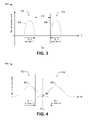
- FIG. 3shows a favorable resistance distribution 300 for a memory array of binary phase change memory cells, where there are two distinct allowable resistance ranges 302 , 304 .
- Each “reliable” cell of the arrayhas a resistance that tends to fail on one of the bell-shaped distributions 306 , 308 , such that some reliable cells 306 tend to be in a “1” state (i.e., in allowable resistance range 302 ) while others cells 308 tend to be in a “0” state (i.e., in allowable resistance range 304 ).
- a sense ampcan accurately write to and read from these reliable cells. For example, in one embodiment, a sense amp could read an accessed cell by comparing the cell's resistance to a reference resistance R REF that represents a resistance of a reference memory cell, which is not in a “1” state or a “0” state.
- the arraymay include unreliable cells in addition to reliable cells, such as shown in FIG. 4 .
- unreliable cellshave resistances 402 that are overlapping or otherwise uncertain.
- Unreliable cellscan arise in several ways. For example, after the memory array is initially manufactured and before the cells are accessed, the cells are often unreliable. Therefore, before a resistive memory can be shipped to a customer, the memory must be conditioned to ensure that the individual memory cells are within specification (i.e., data can be properly written to and read from the individual cells).
- aspects of the present inventionrelate to methods and systems for conditioning unreliable cells to bring their resistances within the allowable resistance ranges. Accordingly, these methods and systems can repair the unreliable cells so correct data may be accurately written to and read from the cells.
- the conditioningshifts the initial (unreliable) resistance of all of the cells to the highest resistance range. For example, in FIG. 3 , resistance range 308 would be the highest resistance range. In other embodiments, the conditioning could shift the initial resistance to any one predetermined resistance range.
- the memory device 500includes a memory array 502 (such as previously discussed array 100 ) and conditioning circuitry 504 .
- the conditioning circuitry 504is configured to apply at least one pulse to at least one bitline associated with any unreliable cells in the memory array 502 .
- This at least one pulseis configured to shift the resistances of the unreliable cells from the unreliable resistance ranges to the reliable resistance ranges, thereby conditioning or repairing the unreliable cells.
- the conditioning circuitry 504could be either off-chip circuitry (e.g., a production line tester used to condition the memory cells prior to commercial distribution) or on-chip circuitry (e.g., built in self-test (BIST) circuitry that is often formed on the same die as the memory array). In some embodiments, this conditioning circuitry 504 could be used a single time prior to commercial distribution of the memory device.
- off-chip circuitrye.g., a production line tester used to condition the memory cells prior to commercial distribution
- on-chip circuitrye.g., built in self-test (BIST) circuitry that is often formed on the same die as the memory array.
- BISTbuilt in self-test
- method 600that sequentially accesses one group of cells after another, conditioning each group of cells as it is accessed. In one embodiment, because of its streamlined processing, this method 600 could be used to condition the cells of the memory array prior to commercial distribution.
- the methodstarts when an indexing variable M is initialized.
- Mcould be set to zero.
- At block 604at least one wordline(M) is asserted to access a group of cells.
- one word line or multiple word linescould be asserted at any given time.
- wordline(M)could access a single cell (bit), a single row of cells (word), multiple rows of cells (sector, block, etc.), or any other number of cells.
- a combination of set and reset pulsescould be applied to the bitlines associated with the accessed cells to condition the cells.
- the method 600determines if all cells in the array have been conditioned. If not (“NO” at 608 ), M is incremented in 610 , and blocks 604 - 608 are repeated until all of the cells in the array are conditioned. After the method has conditioned all of the cells (“YES” at 608 ), the conditioning may end.
- FIG. 7shows a timing diagram 700 that shows of a combination of set and reset pulses that could be applied to the bitlines to condition the cells, in this illustrated embodiment, alternating reset pulses 702 and set pulses 704 are applied.
- the reset pulses 702have a current magnitude I R that is sufficient to heat the programmable volume of the cell above its melting point (which melting point may correspond to approximately I melt ), while the set pulses 704 have a current magnitude I S that heats the programmable volume above I Cryst , which is the current corresponding to the temperature at which some minimal crystallization may occur.
- these alternating set and reset pulses 702 , 704have sufficient current intensify to remove any oxides formed near the top of the heater region under the programmable volume.
- the pulsesalso may change the composition of the programmable volume so proper crystallization may occur. In any event, these pulses may shift the overall resistance of the memory cells from unreliable resistance range to a reliable resistance range, so proper communication with the cell may be achieved.
- method 800that uses successive reset pulses to condition the cells of the array.
- method 800(which may consist essentially of relatively short reset pulses, and not relatively long set pulses) is advantageous in that the array can be conditioned relatively quickly.
- a reset pulsehas a duration of approximately 10 ns
- a set pulsehas a duration of approximately 150 ns.
- each groupwould take at least approximately 800 ns to condition (i.e., 5 set pulses*150 ns+5 reset pulses*10 ns).
- each groupwould take only approximately 100 ns to condition (i.e., 10 reset pulses*10 ns).
- 10 reset pulses*10 nsWhen this example is extended to an array with a large number of cells, such as a 1 gigabyte (GB) array, one can see that significant time savings can be achieved. For production level conditioning, this will allow a manufacturing facility to process more memory devices with fewer production line testers, thereby reducing fabrication costs.
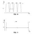
- FIG. 9shows an example of one embodiment of a timing diagram 900 illustrating successive reset pulses 902 that could be used to condition the cells.
- the length and number of successive reset pulsescould vary depending on the implementation.
- somewhat longer reset pulses 1000are applied to condition the cells, which could for example have a duration T R1 of approximately 100 ns and a current magnitude sufficient to melt the programmable volume of a cell's phase-change element
- a single reset pulse 1100is applied to condition the cells, which could, for example, have a duration T R2 of approximately 1000 ns and a current magnitude I R2 sufficient to melt the programmable volume of a cell's phase-change element.
- reset pulsesare Interlaced between groups of cells.
- a reset pulsewill be applied to bitlines of cells in even columns.
- the reset pulsewill not be applied to all bitlines, but rather only to a group of 1, 2, 4. 8, 16 . . . N bitlines.
- another reset pulsewill be applied to the bitlines of cells in odd columns.
- the methodoptionally determines whether more conditioning pulses need to be applied to the cell.
- blocks 1206 - 1210are repeated, if the accessed cells are sufficiently conditioned (“NO” at 1210 ), the method progresses to block 1212 and determines if all the cells in the array have been conditioned, if not (“NO” at 1212 ), then M is incremented in 1214 and the appropriate blocks are repeated until all of the cells in the array have been conditioned.
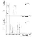
- FIGS. 13A-13Bshow a sample timing diagram 1300 that shows interlaced pulses.
- successive reset pulsesare interlaced between even columns and odd columns of cells.
- a reset pulse 1302is applied to the odd columns of cells.
- a reset pulse 1304is applied to the even columns of cells.
- charge pumps on the chiptypically drive the bitlines. Because these charge pumps can only drive a limited amount of current as a practical matter (due to area concerns on the chip), this interlacing provides an effective method of parallelizing conditioning In some instances. Although not illustrated, the interlacing could also be performed between words, pages, blocks, etc.
- the cellsbefore the cells are conditioned, the cells screened to determine whether they are unreliable. In this embodiment, only unreliable cells then receive conditioning. This method may be quicker and provide greater throughput because fewer cells may need to be conditioned. A more detailed discussion in set forth below.
- the indexing variable Mis initialized. Again, M could be set to “0”, for example.
- wordline(M)is asserted to access a group of cells.
- Test datais written to the accessed cells by applying a suitable pulse on the bitlines associated with the cells.
- wordline(M)is asserted to read the data back from the accessed cells.
- the methoddetermines if the read data favorable compares to the test data. If the memory cells and accompanying circuitry are working properly (i.e., the cells are reliable cells), the read data should equal the test data. In one embodiment, this comparison could comprise a logical XOR or XNOR function, such that if any read bits differ from corresponding test bits then any errant bits can be uniquely identified. In other embodiments, error-code-checking (ECC), parity bits, or other algorithms could be used.
- ECCerror-code-checking
- the read datadoes equal the test data (“YES” at 1408 )
- the accessed cellsare considered properly conditioned and the method progresses to block 1410 .
- the methodthen moves to 1412 and determines if other cells should be analyzed.
- the methodmay assume that the group includes unreliable cells and may identify precisely which cells are unreliable in block 1416 . These unreliable cells may then be conditioned as necessary.
- the methodmay perform optional cycling steps 1418 , 1420 . This cycling would likely eliminate bad results due to one-time errors such as alpha-particles or other radiation that could alter the bits of the cells.
- a data processing system 1500that comprises data processing circuitry 1502 configured to process data; and a memory device 1504 for storing the data.
- the memory devicemay be any memory device as described herein.
- the memory device 1504can include an array of phase change memory cells where the processing circuitry could include conditioning circuitry as described herein.
- the data processing system 1500could be a communication device, such as a cell phone or pager, for example.
- the data processing system 1500could be a portable electronic product, such as a portable computer, cell phone, pager, camera, music device, voice recorder, etc.
- the data processing system 1500could comprise an electronic system, such as a car, plane, industrial control system, etc.
- FIG. 16shows a resistance distribution of the multi-bit cell, which again shows one general scheme in which a range of resistances can be divided into a number of allowable resistance ranges.
Landscapes
- Engineering & Computer Science (AREA)
- Chemical & Material Sciences (AREA)
- Computer Hardware Design (AREA)
- Materials Engineering (AREA)
- Crystallography & Structural Chemistry (AREA)
- Semiconductor Memories (AREA)
Abstract
Description
- This application claims priority to U.S. Provisional Application Ser. No. 60/947,328 filed Jun. 29, 2007, entitled “CONDITIONING OPERATIONS FOR MEMORY CELLS.”
- The present invention relates generally to semiconductor devices and mere particularly to improved methods and systems for semiconductor memories.
- Several trends presently exist in the semiconductor and electronics industry. One of these trends is that recent generations of portable electronic devices are using more memory than previous generations. This increase in memory allows these new devices to store more data, such as music or images, and also provides the devices with more computational power and speed.
- One type of memory device includes an array of resistive memory cells, where individual bits of data can be stored in the individual resistive memory cells of the array. Depending on how the cells of the array are biased, each cell can be put into a more resistive state or a less resistive state. In real world-implementations, the more resistive state can be associated with a logical “1” and the less resistive state can be associated with a logical “0”, or vice versa. Therefore, by switching between the resistive states, a user can store any combination of “1”s and “0”s in the array, which could correspond to digitally encoded music, images, software, etc.
- Typically, users expect their data to be stored accurately in these memory devices. As such, there is an on-going need to provide memory systems, devices, and methods that can provide accurate data storage in memory.
- One embodiment of the invention relates to a method for conditioning resistive memory cells of a memory array with a number of reliable resistance ranges, where each reliable resistance range corresponds to a different data state. In the method, group of at least one resistive memory cell is accessed, which group includes at least one unreliable cell. At least one pulse is applied to the at least one unreliable cell to shift at least one resistance respectively associated with the at least one unreliable cell to the highest of the reliable resistance ranges. Other methods and systems are also disclosed.
FIG. 1 shows one embodiment of a memory array of resistive memory cells;FIG. 2 shows one embodiment of a phase-change memory element;FIG. 3 shows one embodiment of a favorable resistance distribution that relates to an array of binary resistive memory cells;FIG. 4 shows one embodiment of an unfavorable resistance distribution that relates to an array of binary resistive memory cells;FIG. 5 shows one embodiment of a memory device that is coupled to conditioning circuitry;FIG. 6 shows one flowchart of a memory conditioning operation;FIG. 7 shows a timing diagram;FIG. 8 shows another flowchart of a memory conditioning operation;FIG. 9 shows another timing diagram;FIG. 10 shows another timing diagram;FIG. 11 shows another timing diagram;FIG. 12 shows another flowchart of a memory conditioning operation:FIG. 13A-13B show additional timing diagrams;FIG. 14 shows another flowchart of a memory conditioning operation;FIG. 15 is a block diagram of a data processing system In which exemplary memory devices may be utilized; andFIG. 16 shows one embodiment of a resistance distribution that relates to an array of multi-bit resistive memory cells.- One or more Implementations of the present invention will now be described with reference to the attached drawings, wherein like reference numerals are used to refer to like elements throughout. The drawings are not necessarily drawn to scale.
- Although several embodiments are illustrated and discussed below in the context of resistive or phase-change memories, aspects of the present invention could also relate to other types of memory devices and methods associated therewith. Some examples of illustrative types of resistive memory include: perovskite memory, binary oxides random access memory (OxRAM), phase change random access memory (PCRAM), and conductive bridging random access memory (CBRAM).
- Referring now to
FIG. 1 , one can see amemory array 100 that includes a number ofmemory cells 102 that are each capable of storing one or more bits of data, depending on the implementation. Thecells 102 are arranged in M rows (e.g., words) and N columns (e.g., bits), indicated as CROW,COLUMN. Each row of cells is an N bit data word accessible by activation of a wordline WL associated with that row. For example, in the first row of thearray 100, the cells C1,1through C1,Nform an N bit data word that may be accessible by activation of wordline WL1 via bitlines BL1 through BLN. Generally speaking, while a wordline is asserted, biasing pulses can be applied to the bitlines to program the cells of the corresponding row. - The illustrated
array 100 is configured in a single-ended configuration, where a single bitline is coupled to each column of cells. Thus, individual bits of an accessed wordline can be programmed to “1”s and “0”s by applying suitable biasing pulses to the bitlines. - As shown, each memory cell can include a resistive element150 (e.g., a layer of programmable material), and an
access transistor 152. In other non-illustrated embodiments, a diode could be substituted in place of eachaccess transistor 152. - In one embodiment, the
resistive elements 150 could comprise phase change elements, such as thephase change element 200 shown InFIG. 2 . Thephase change element 200 includes a layer of programmable material202 (e.g., a polycrystalline chalcogenide material, such as GeSbTe or an AgInSbTe compound, or a chalcogenide-free material, such as GeSb or GaSb) that is positioned between atop electrode 204 and abottom electrode 206. In the illustrated embodiment, thebottom electrode 206 includes aheater member 208 that can, by means of an appropriate pulse configuration applied to the cell's bitline while the cell is accessed, place aprogrammable volume 210 of the programmable material in either an amorphous-state (i.e., relatively-high resistance state) or a crystalline state (i.e., relatively-low resistance state). These states could then be assigned to corresponding data states. For example, the amorphous-state could be assigned to a logical “0” and the crystalline-state could he assigned to a logical “1”, or vice versa. In various embodiments, additional resistance states could be associated with corresponding data states to implement a multi-bit cell with more than two states per cell. - Because or slight variations between the memory cells of the array, the resistances of the cells can vary across the array. Thus,
FIG. 3 shows afavorable resistance distribution 300 for a memory array of binary phase change memory cells, where there are two distinctallowable resistance ranges shaped distributions reliable cells 306 tend to be in a “1” state (i.e., in allowable resistance range302) whileothers cells 308 tend to be in a “0” state (i.e., in allowable resistance range304). Because there issufficient margin 310 between the twostates - In some cases, however, the array may include unreliable cells in addition to reliable cells, such as shown in
FIG. 4 . As shown, unreliable cells haveresistances 402 that are overlapping or otherwise uncertain. - Unreliable cells can arise in several ways. For example, after the memory array is initially manufactured and before the cells are accessed, the cells are often unreliable. Therefore, before a resistive memory can be shipped to a customer, the memory must be conditioned to ensure that the individual memory cells are within specification (i.e., data can be properly written to and read from the individual cells).
- To initially prepare the memory for a customer, aspects of the present invention relate to methods and systems for conditioning unreliable cells to bring their resistances within the allowable resistance ranges. Accordingly, these methods and systems can repair the unreliable cells so correct data may be accurately written to and read from the cells. In one embodiment, the conditioning shifts the initial (unreliable) resistance of all of the cells to the highest resistance range. For example, in
FIG. 3 ,resistance range 308 would be the highest resistance range. In other embodiments, the conditioning could shift the initial resistance to any one predetermined resistance range. - Referring now to
FIG. 5 , one can see amemory device 500 that is configured to condition unreliable cells. Thememory device 500 includes a memory array502 (such as previously discussed array100) andconditioning circuitry 504. Generally speaking, theconditioning circuitry 504 is configured to apply at least one pulse to at least one bitline associated with any unreliable cells in thememory array 502. This at least one pulse is configured to shift the resistances of the unreliable cells from the unreliable resistance ranges to the reliable resistance ranges, thereby conditioning or repairing the unreliable cells. - Depending on the Implementation, the
conditioning circuitry 504 could be either off-chip circuitry (e.g., a production line tester used to condition the memory cells prior to commercial distribution) or on-chip circuitry (e.g., built in self-test (BIST) circuitry that is often formed on the same die as the memory array). In some embodiments, thisconditioning circuitry 504 could be used a single time prior to commercial distribution of the memory device. - More detailed functionality of the
memory array 502 andconditioning circuitry 504 in various embodiments will be appreciated with reference to the following methods. Several illustrative methods (600,800,1200, and1400) are now set forth below with reference to several flowcharts (FIG. 6 ,FIG. 8 ,FIG. 12 , andFIG. 14 , respectively). Although these methods are illustrated and described below as a series of acts or events, it will be appreciated that the present invention is not limited by the illustrated ordering of such acts or events. For example, some acts may occur in different orders and/or concurrently with other acts or events apart from those illustrated and/or described herein, in accordance with the invention. In addition, not all illustrated steps may be required to implement a methodology in accordance with the present invention. Furthermore, the methods according to the present invention may be implemented in association with the devices and systems illustrated and described herein (e.g.,memory device 500 inFIG. 5 ) as well as in association with other structures not illustrated. - Referring now to
FIG. 6 , one can seemethod 600 that sequentially accesses one group of cells after another, conditioning each group of cells as it is accessed. In one embodiment, because of its streamlined processing, thismethod 600 could be used to condition the cells of the memory array prior to commercial distribution. - At
block 602, the method starts when an indexing variable M is initialized. For example, M could be set to zero. - At
block 604, at least one wordline(M) is asserted to access a group of cells. In various embodiments, one word line or multiple word lines could be asserted at any given time. Thus, wordline(M) could access a single cell (bit), a single row of cells (word), multiple rows of cells (sector, block, etc.), or any other number of cells. - At
block 606, a combination of set and reset pulses could be applied to the bitlines associated with the accessed cells to condition the cells. Atblock 608, themethod 600 determines if all cells in the array have been conditioned. If not (“NO” at608), M is incremented in610, and blocks604-608 are repeated until all of the cells in the array are conditioned. After the method has conditioned all of the cells (“YES” at608), the conditioning may end. FIG. 7 shows a timing diagram700 that shows of a combination of set and reset pulses that could be applied to the bitlines to condition the cells, in this illustrated embodiment, alternatingreset pulses 702 and setpulses 704 are applied. In the context of a phase change memory cell (e.g.,cell 200 ofFIG. 2 ), thereset pulses 702 have a current magnitude IRthat is sufficient to heat the programmable volume of the cell above its melting point (which melting point may correspond to approximately Imelt), while theset pulses 704 have a current magnitude ISthat heats the programmable volume above ICryst, which is the current corresponding to the temperature at which some minimal crystallization may occur. Often these alternating set and resetpulses - Referring now to
FIG. 8 , one can see anothermethod 800 that uses successive reset pulses to condition the cells of the array. When compared tomethod 700, method800 (which may consist essentially of relatively short reset pulses, and not relatively long set pulses) is advantageous in that the array can be conditioned relatively quickly. For purposes of illustration, consider two cases when ten successive pulses are used to condition each group of cells, where a reset pulse has a duration of approximately 10 ns and a set pulse has a duration of approximately 150 ns. Inmethod 700, each group would take at least approximately 800 ns to condition (i.e., 5 set pulses*150 ns+5 reset pulses*10 ns). By contrast, inmethod 800, each group would take only approximately 100 ns to condition (i.e., 10 reset pulses*10 ns). When this example is extended to an array with a large number of cells, such as a 1 gigabyte (GB) array, one can see that significant time savings can be achieved. For production level conditioning, this will allow a manufacturing facility to process more memory devices with fewer production line testers, thereby reducing fabrication costs. FIG. 9 shows an example of one embodiment of a timing diagram900 illustratingsuccessive reset pulses 902 that could be used to condition the cells. As shown inFIGS. 10-11 , the length and number of successive reset pulses could vary depending on the implementation. InFIG. 10 , somewhat longer resetpulses 1000 are applied to condition the cells, which could for example have a duration TR1of approximately 100 ns and a current magnitude sufficient to melt the programmable volume of a cell's phase-change element, inFIG. 11 , asingle reset pulse 1100 is applied to condition the cells, which could, for example, have a duration TR2of approximately 1000 ns and a current magnitude IR2sufficient to melt the programmable volume of a cell's phase-change element.- Referring now to
FIG. 12 , one can see still anothermethod 1200 that can be used to condition the memory cells, in this method, reset pulses (or other pulses) are Interlaced between groups of cells. Thus, inblock 1206 during a first time period, a reset pulse will be applied to bitlines of cells in even columns. In one embodiment, the reset pulse will not be applied to all bitlines, but rather only to a group of 1, 2, 4. 8, 16 . . . N bitlines. Inblock 1208, during the next time period, another reset pulse will be applied to the bitlines of cells in odd columns. Inblock 1210, the method optionally determines whether more conditioning pulses need to be applied to the cell. If more conditioning pulses are needed (“YES” at1210), blocks1206-1210 are repeated, if the accessed cells are sufficiently conditioned (“NO” at1210), the method progresses to block1212 and determines if all the cells in the array have been conditioned, if not (“NO” at1212), then M is incremented in1214 and the appropriate blocks are repeated until all of the cells in the array have been conditioned. FIGS. 13A-13B show a sample timing diagram1300 that shows interlaced pulses. In this illustrated embodiment, successive reset pulses are interlaced between even columns and odd columns of cells. Thus, during time period T1, areset pulse 1302 is applied to the odd columns of cells. During time period T2a reset pulse1304 is applied to the even columns of cells. With BIST and other on-chip conditioning circuitry, charge pumps on the chip typically drive the bitlines. Because these charge pumps can only drive a limited amount of current as a practical matter (due to area concerns on the chip), this interlacing provides an effective method of parallelizing conditioning In some instances. Although not illustrated, the interlacing could also be performed between words, pages, blocks, etc.- Referring to
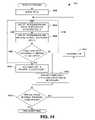
FIG. 14 , one can see anothermethod 1400 in accordance with aspect of the invention. In this method, before the cells are conditioned, the cells screened to determine whether they are unreliable. In this embodiment, only unreliable cells then receive conditioning. This method may be quicker and provide greater throughput because fewer cells may need to be conditioned. A more detailed discussion in set forth below. - In
block 1402, the indexing variable M is initialized. Again, M could be set to “0”, for example. - In
block 1404, wordline(M) is asserted to access a group of cells. Test data is written to the accessed cells by applying a suitable pulse on the bitlines associated with the cells. - In
block 1406, wordline(M) is asserted to read the data back from the accessed cells. - In
block 1408, the method determines if the read data favorable compares to the test data. If the memory cells and accompanying circuitry are working properly (i.e., the cells are reliable cells), the read data should equal the test data. In one embodiment, this comparison could comprise a logical XOR or XNOR function, such that if any read bits differ from corresponding test bits then any errant bits can be uniquely identified. In other embodiments, error-code-checking (ECC), parity bits, or other algorithms could be used. - If the read data does equal the test data (“YES” at1408), the accessed cells are considered properly conditioned and the method progresses to block1410. The method then moves to1412 and determines if other cells should be analyzed.
- If the read data does not equal the test data (“NO” in1408), however, the method may assume that the group includes unreliable cells and may identify precisely which cells are unreliable in
block 1416. These unreliable cells may then be conditioned as necessary. - To ensure that the result of
block 1408 is accurate, the method may performoptional cycling steps - Referring now to
FIG. 15 , one can see an embodiment of adata processing system 1500 that comprisesdata processing circuitry 1502 configured to process data; and amemory device 1504 for storing the data. The memory device may be any memory device as described herein. For example, in one embodiment, thememory device 1504 can include an array of phase change memory cells where the processing circuitry could include conditioning circuitry as described herein. In one embodiment thedata processing system 1500 could be a communication device, such as a cell phone or pager, for example. In other embodiments, thedata processing system 1500 could be a portable electronic product, such as a portable computer, cell phone, pager, camera, music device, voice recorder, etc. In still other embodiments, thedata processing system 1500 could comprise an electronic system, such as a car, plane, industrial control system, etc. - While one embodiment of a binary phase change memory cell has been discussed for convenience and clarity, aspects of the present invention also relate to multi-bit memory cells (e.g., multi-bit phase change memory cells, multi-bit flash cells, multi-bit resistive cells, etc), such as quad-hit cells or even higher-order-bit cells.
FIG. 16 shows a resistance distribution of the multi-bit cell, which again shows one general scheme in which a range of resistances can be divided into a number of allowable resistance ranges. These multi-bit memory cells could also drift to from the favorable distribution, creating unreliable cells as described above. - While the invention has been illustrated and described with respect to one or more implementations, alterations and/or modifications may be made to the illustrated examples without departing from the spirit and scope of the appended claims. For example, although the term “number” may be used, it will be construed broadly to include any positive integer ranging from two to practically infinity, in particular regard to the various functions performed by the above described components or structures (assemblies, devices, circuits, systems, etc.), the terms (including a reference to a “means”) used to describe such components are intended to correspond, unless otherwise indicated, to any component or structure which performs the specified function of the described component (e.g., that is functionally equivalent), even though not structurally equivalent to the disclosed structure which performs the function in the herein illustrated exemplary implementations of the invention. In addition, while a particular feature of the invention may have been disclosed with respect to only one of several implementations, such feature may be combined with one or more other features of the other implementations as may be desired and advantageous for any given or particular application. Furthermore, to the extent that the terms “including”, “includes”, “having”, “has”, “with”, or variants thereof are used in either the detailed description and the claims, such terms are intended to be inclusive in a manner similar to the term “comprising”.
Claims (27)
Priority Applications (2)
| Application Number | Priority Date | Filing Date | Title |
|---|---|---|---|
| US11/778,786US7646625B2 (en) | 2007-06-29 | 2007-07-17 | Conditioning operations for memory cells |
| DE102008030859ADE102008030859A1 (en) | 2007-06-29 | 2008-06-30 | Method of conditioning resistive memory cells of memory array, involves applying pulse to unreliable cell such that pulse shifts resistance respectively associated with unreliable cell to predetermined reliable resistance range |
Applications Claiming Priority (2)
| Application Number | Priority Date | Filing Date | Title |
|---|---|---|---|
| US94732807P | 2007-06-29 | 2007-06-29 | |
| US11/778,786US7646625B2 (en) | 2007-06-29 | 2007-07-17 | Conditioning operations for memory cells |
Publications (2)
| Publication Number | Publication Date |
|---|---|
| US20090003035A1true US20090003035A1 (en) | 2009-01-01 |
| US7646625B2 US7646625B2 (en) | 2010-01-12 |
Family
ID=40157567
Family Applications (1)
| Application Number | Title | Priority Date | Filing Date |
|---|---|---|---|
| US11/778,786Expired - Fee RelatedUS7646625B2 (en) | 2007-06-29 | 2007-07-17 | Conditioning operations for memory cells |
Country Status (2)
| Country | Link |
|---|---|
| US (1) | US7646625B2 (en) |
| DE (1) | DE102008030859A1 (en) |
Cited By (13)
| Publication number | Priority date | Publication date | Assignee | Title |
|---|---|---|---|---|
| US20090141546A1 (en)* | 2007-11-29 | 2009-06-04 | Samsung Electronics Co., Ltd. | Method of operating a phase-change memory device |
| US20090225583A1 (en)* | 2008-03-05 | 2009-09-10 | Samsung Electronics Co., Ltd. | Resistive memory device for programming resistance conversion layers and method thereof |
| US20100067290A1 (en)* | 2008-09-15 | 2010-03-18 | Savransky Semyon D | Method of programming of phase-change memory and associated devices and materials |
| US20110069540A1 (en)* | 2009-09-23 | 2011-03-24 | Savransky Semyon D | Method of a phase-change memory programming |
| US20120120710A1 (en)* | 2010-11-17 | 2012-05-17 | Peter Rabkin | Memory system with reversible resistivity-switching using pulses of alternatrie polarity |
| WO2013061191A1 (en)* | 2011-10-28 | 2013-05-02 | International Business Machines Corporation | Conditioning phase change memory cells |
| WO2013170214A3 (en)* | 2012-05-11 | 2014-01-23 | Adesto Technologies Corporation | Resistive devices and methods of operation thereof |
| WO2014133912A1 (en)* | 2013-02-28 | 2014-09-04 | Sandisk 3D Llc | Reram forming with reset and iload compensation |
| US8953362B2 (en) | 2012-05-11 | 2015-02-10 | Adesto Technologies Corporation | Resistive devices and methods of operation thereof |
| US20160263437A1 (en)* | 2014-08-26 | 2016-09-15 | Well Being Digital Limited | A gait monitor and a method of monitoring the gait of a person |
| US20190108882A1 (en)* | 2017-10-10 | 2019-04-11 | Arm Ltd. | Method, system and device for testing correlated electron switch (ces) devices |
| EP3537443A1 (en)* | 2018-03-09 | 2019-09-11 | Commissariat à l'Energie Atomique et aux Energies Alternatives | Method for analogue programming of a phase-changing memory cell by means of identical electrical pulses |
| TWI764762B (en)* | 2020-07-31 | 2022-05-11 | 華邦電子股份有限公司 | Array device and writing method thereof |
Families Citing this family (5)
| Publication number | Priority date | Publication date | Assignee | Title |
|---|---|---|---|---|
| JP2012244180A (en) | 2011-05-24 | 2012-12-10 | Macronix Internatl Co Ltd | Multi-layer structure and manufacturing method for the same |
| US8804399B2 (en)* | 2012-03-23 | 2014-08-12 | Micron Technology, Inc. | Multi-function resistance change memory cells and apparatuses including the same |
| US9952796B2 (en) | 2014-01-31 | 2018-04-24 | Hewlett Packard Enterprise Development Lp | Data storing in memory arrays |
| US9336878B2 (en)* | 2014-06-18 | 2016-05-10 | Macronix International Co., Ltd. | Method and apparatus for healing phase change memory devices |
| US12200925B2 (en) | 2022-04-19 | 2025-01-14 | Macronix International Co., Ltd. | Capacitors in memory devices |
Citations (5)
| Publication number | Priority date | Publication date | Assignee | Title |
|---|---|---|---|---|
| US6396742B1 (en)* | 2000-07-28 | 2002-05-28 | Silicon Storage Technology, Inc. | Testing of multilevel semiconductor memory |
| US20020167838A1 (en)* | 2001-05-14 | 2002-11-14 | Perner Frederick A. | Resistive cross point memory with on-chip sense amplifier calibration method and apparatus |
| US20030074152A1 (en)* | 2001-10-09 | 2003-04-17 | Kessenich Jeffrey Alan | System and method of testing non-volatile memory cells |
| US20050128855A1 (en)* | 2003-12-15 | 2005-06-16 | Joshi Rajiv V. | Self timed bit and read/write pulse stretchers |
| US20070034908A1 (en)* | 2005-08-10 | 2007-02-15 | Woo-Yeong Cho | Phase change random access memory device |
- 2007
- 2007-07-17USUS11/778,786patent/US7646625B2/ennot_activeExpired - Fee Related
- 2008
- 2008-06-30DEDE102008030859Apatent/DE102008030859A1/ennot_activeWithdrawn
Patent Citations (5)
| Publication number | Priority date | Publication date | Assignee | Title |
|---|---|---|---|---|
| US6396742B1 (en)* | 2000-07-28 | 2002-05-28 | Silicon Storage Technology, Inc. | Testing of multilevel semiconductor memory |
| US20020167838A1 (en)* | 2001-05-14 | 2002-11-14 | Perner Frederick A. | Resistive cross point memory with on-chip sense amplifier calibration method and apparatus |
| US20030074152A1 (en)* | 2001-10-09 | 2003-04-17 | Kessenich Jeffrey Alan | System and method of testing non-volatile memory cells |
| US20050128855A1 (en)* | 2003-12-15 | 2005-06-16 | Joshi Rajiv V. | Self timed bit and read/write pulse stretchers |
| US20070034908A1 (en)* | 2005-08-10 | 2007-02-15 | Woo-Yeong Cho | Phase change random access memory device |
Cited By (26)
| Publication number | Priority date | Publication date | Assignee | Title |
|---|---|---|---|---|
| US8116125B2 (en)* | 2007-11-29 | 2012-02-14 | Samsung Electronics Co., Ltd. | Method of operating a phase-change memory device |
| US20090141546A1 (en)* | 2007-11-29 | 2009-06-04 | Samsung Electronics Co., Ltd. | Method of operating a phase-change memory device |
| US20090225583A1 (en)* | 2008-03-05 | 2009-09-10 | Samsung Electronics Co., Ltd. | Resistive memory device for programming resistance conversion layers and method thereof |
| US7940547B2 (en)* | 2008-03-05 | 2011-05-10 | Samsung Electronics Co., Ltd. | Resistive memory device for programming resistance conversion layers and method thereof |
| US20100067290A1 (en)* | 2008-09-15 | 2010-03-18 | Savransky Semyon D | Method of programming of phase-change memory and associated devices and materials |
| US20110069540A1 (en)* | 2009-09-23 | 2011-03-24 | Savransky Semyon D | Method of a phase-change memory programming |
| US8462580B2 (en)* | 2010-11-17 | 2013-06-11 | Sandisk 3D Llc | Memory system with reversible resistivity-switching using pulses of alternatrie polarity |
| US20120120710A1 (en)* | 2010-11-17 | 2012-05-17 | Peter Rabkin | Memory system with reversible resistivity-switching using pulses of alternatrie polarity |
| US9558817B2 (en) | 2011-10-28 | 2017-01-31 | International Business Machines Corporation | Conditioning phase change memory cells |
| CN103890851A (en)* | 2011-10-28 | 2014-06-25 | 国际商业机器公司 | Conditioning phase change memory cells |
| WO2013061191A1 (en)* | 2011-10-28 | 2013-05-02 | International Business Machines Corporation | Conditioning phase change memory cells |
| US9734902B2 (en) | 2012-05-11 | 2017-08-15 | Adesto Technologies Corporation | Resistive memory device with ramp-up/ramp-down program/erase pulse |
| CN104221090A (en)* | 2012-05-11 | 2014-12-17 | 爱德斯托科技有限公司 | Resistive devices and methods of operation thereof |
| US8953362B2 (en) | 2012-05-11 | 2015-02-10 | Adesto Technologies Corporation | Resistive devices and methods of operation thereof |
| US9165644B2 (en) | 2012-05-11 | 2015-10-20 | Axon Technologies Corporation | Method of operating a resistive memory device with a ramp-up/ramp-down program/erase pulse |
| US9431101B2 (en) | 2012-05-11 | 2016-08-30 | Adesto Technologies Corporation | Resistive devices and methods of operation thereof |
| WO2013170214A3 (en)* | 2012-05-11 | 2014-01-23 | Adesto Technologies Corporation | Resistive devices and methods of operation thereof |
| WO2014133912A1 (en)* | 2013-02-28 | 2014-09-04 | Sandisk 3D Llc | Reram forming with reset and iload compensation |
| US9007810B2 (en) | 2013-02-28 | 2015-04-14 | Sandisk 3D Llc | ReRAM forming with reset and iload compensation |
| US20160263437A1 (en)* | 2014-08-26 | 2016-09-15 | Well Being Digital Limited | A gait monitor and a method of monitoring the gait of a person |
| US20190108882A1 (en)* | 2017-10-10 | 2019-04-11 | Arm Ltd. | Method, system and device for testing correlated electron switch (ces) devices |
| US10714175B2 (en)* | 2017-10-10 | 2020-07-14 | ARM, Ltd. | Method, system and device for testing correlated electron switch (CES) devices |
| EP3537443A1 (en)* | 2018-03-09 | 2019-09-11 | Commissariat à l'Energie Atomique et aux Energies Alternatives | Method for analogue programming of a phase-changing memory cell by means of identical electrical pulses |
| FR3078814A1 (en)* | 2018-03-09 | 2019-09-13 | Commissariat A L'energie Atomique Et Aux Energies Alternatives | METHOD FOR ANALOGALLY PROGRAMMING A PHASE CHANGE MEMORY CELL USING IDENTICAL ELECTRIC PULSES |
| US10755754B2 (en) | 2018-03-09 | 2020-08-25 | Commissariat A L'energie Atomique Et Aux Energies Alternatives | Analog method for programming a phase change memory cell by means of identical electrical pulses |
| TWI764762B (en)* | 2020-07-31 | 2022-05-11 | 華邦電子股份有限公司 | Array device and writing method thereof |
Also Published As
| Publication number | Publication date |
|---|---|
| US7646625B2 (en) | 2010-01-12 |
| DE102008030859A1 (en) | 2009-01-29 |
Similar Documents
| Publication | Publication Date | Title |
|---|---|---|
| US7646625B2 (en) | Conditioning operations for memory cells | |
| US7969798B2 (en) | Phase change memory devices and read methods using elapsed time-based read voltages | |
| US8830728B2 (en) | Resistance change memory device and current trimming method thereof | |
| KR101460954B1 (en) | Stabilization of resistive memory | |
| US7548451B2 (en) | Phase change random access memory | |
| US7486536B2 (en) | Phase-changeable memory device and method of programming the same | |
| US7573758B2 (en) | Phase-change random access memory (PRAM) performing program loop operation and method of programming the same | |
| US8081501B2 (en) | Multi-level nonvolatile memory device using variable resistive element | |
| US7916524B2 (en) | Program method with locally optimized write parameters | |
| US8787065B2 (en) | Apparatuses and methods for determining stability of a memory cell | |
| US8345464B2 (en) | Resistive memory devices having a stacked structure and methods of operation thereof | |
| US7751232B2 (en) | Method of testing PRAM device | |
| US20090161415A1 (en) | Integrated circuit for setting a memory cell based on a reset current distribution | |
| US20100232208A1 (en) | Method of executing a forming operation to variable resistance element | |
| WO2004055827A1 (en) | Method and system to store information | |
| KR20150064108A (en) | Drift acceleration in resistance variable memory | |
| CN101140802A (en) | Phase change random access memory and related operation method | |
| US9443586B2 (en) | Nonvolatile memory device, memory system including the same and method for driving nonvolatile memory device | |
| US8897063B2 (en) | Multilevel differential sensing in phase change memory | |
| US10204037B2 (en) | Memory device, memory controller and operation method thereof | |
| KR20160015992A (en) | Nonvolatile memory device and method for sensing the same | |
| KR20180081333A (en) | Memory device comprising resistance change material method for operating the memory device | |
| KR20080041936A (en) | Defect cell detection method of phase change memory and semiconductor memory device using the method |
Legal Events
| Date | Code | Title | Description |
|---|---|---|---|
| AS | Assignment | Owner name:QIMONDA NORTH AMERICA CORP., NORTH CAROLINA Free format text:ASSIGNMENT OF ASSIGNORS INTEREST;ASSIGNORS:PHILIPP, JAN BORIS;HAPP, THOMAS;REEL/FRAME:021113/0807 Effective date:20070710 Owner name:INFINEON TECHNOLOGIES NORTH AMERICA CORP., CALIFOR Free format text:ASSIGNMENT OF ASSIGNORS INTEREST;ASSIGNOR:NIRSCHL, THOMAS;REEL/FRAME:021113/0882 Effective date:20070715 | |
| AS | Assignment | Owner name:QIMONDA NORTH AMERICA CORP., NORTH CAROLINA Free format text:ASSIGNMENT OF ASSIGNORS INTEREST;ASSIGNOR:INFINEON TECHNOLOGIES NORTH AMERICA CORP.;REEL/FRAME:021752/0351 Effective date:20081024 | |
| FEPP | Fee payment procedure | Free format text:PAYOR NUMBER ASSIGNED (ORIGINAL EVENT CODE: ASPN); ENTITY STATUS OF PATENT OWNER: LARGE ENTITY | |
| AS | Assignment | Owner name:QIMONDA AG, GERMANY Free format text:ASSIGNMENT OF ASSIGNORS INTEREST;ASSIGNOR:QIMONDA NORTH AMERICA CORP;REEL/FRAME:026138/0613 Effective date:20110221 | |
| FPAY | Fee payment | Year of fee payment:4 | |
| AS | Assignment | Owner name:INFINEON TECHNOLOGIES AG, GERMANY Free format text:ASSIGNMENT OF ASSIGNORS INTEREST;ASSIGNOR:QIMONDA AG;REEL/FRAME:035623/0001 Effective date:20141009 | |
| AS | Assignment | Owner name:POLARIS INNOVATIONS LIMITED, IRELAND Free format text:ASSIGNMENT OF ASSIGNORS INTEREST;ASSIGNOR:INFINEON TECHNOLOGIES AG;REEL/FRAME:037254/0782 Effective date:20150708 | |
| FEPP | Fee payment procedure | Free format text:MAINTENANCE FEE REMINDER MAILED (ORIGINAL EVENT CODE: REM.) | |
| LAPS | Lapse for failure to pay maintenance fees | Free format text:PATENT EXPIRED FOR FAILURE TO PAY MAINTENANCE FEES (ORIGINAL EVENT CODE: EXP.) | |
| STCH | Information on status: patent discontinuation | Free format text:PATENT EXPIRED DUE TO NONPAYMENT OF MAINTENANCE FEES UNDER 37 CFR 1.362 | |
| FP | Lapsed due to failure to pay maintenance fee | Effective date:20180112 |