US20090001504A1 - Method for Transferring Semiconductor Element, Method for Manufacturing Semiconductor Device, and Semiconductor Device - Google Patents
Method for Transferring Semiconductor Element, Method for Manufacturing Semiconductor Device, and Semiconductor DeviceDownload PDFInfo
- Publication number
- US20090001504A1 US20090001504A1US12/162,568US16256806AUS2009001504A1US 20090001504 A1US20090001504 A1US 20090001504A1US 16256806 AUS16256806 AUS 16256806AUS 2009001504 A1US2009001504 A1US 2009001504A1
- Authority
- US
- United States
- Prior art keywords
- substrate
- semiconductor element
- temporary supporting
- supporting substrate
- semiconductor
- Prior art date
- Legal status (The legal status is an assumption and is not a legal conclusion. Google has not performed a legal analysis and makes no representation as to the accuracy of the status listed.)
- Granted
Links
Images


Classifications
- H—ELECTRICITY
- H01—ELECTRIC ELEMENTS
- H01L—SEMICONDUCTOR DEVICES NOT COVERED BY CLASS H10
- H01L21/00—Processes or apparatus adapted for the manufacture or treatment of semiconductor or solid state devices or of parts thereof
- H01L21/02—Manufacture or treatment of semiconductor devices or of parts thereof
- H01L21/04—Manufacture or treatment of semiconductor devices or of parts thereof the devices having potential barriers, e.g. a PN junction, depletion layer or carrier concentration layer
- H01L21/18—Manufacture or treatment of semiconductor devices or of parts thereof the devices having potential barriers, e.g. a PN junction, depletion layer or carrier concentration layer the devices having semiconductor bodies comprising elements of Group IV of the Periodic Table or AIIIBV compounds with or without impurities, e.g. doping materials
- H01L21/26—Bombardment with radiation
- H01L21/263—Bombardment with radiation with high-energy radiation
- H01L21/265—Bombardment with radiation with high-energy radiation producing ion implantation
- H01L21/26506—Bombardment with radiation with high-energy radiation producing ion implantation in group IV semiconductors
- H01L21/26513—Bombardment with radiation with high-energy radiation producing ion implantation in group IV semiconductors of electrically active species
- H—ELECTRICITY
- H01—ELECTRIC ELEMENTS
- H01L—SEMICONDUCTOR DEVICES NOT COVERED BY CLASS H10
- H01L21/00—Processes or apparatus adapted for the manufacture or treatment of semiconductor or solid state devices or of parts thereof
- H01L21/02—Manufacture or treatment of semiconductor devices or of parts thereof
- H01L21/04—Manufacture or treatment of semiconductor devices or of parts thereof the devices having potential barriers, e.g. a PN junction, depletion layer or carrier concentration layer
- H01L21/18—Manufacture or treatment of semiconductor devices or of parts thereof the devices having potential barriers, e.g. a PN junction, depletion layer or carrier concentration layer the devices having semiconductor bodies comprising elements of Group IV of the Periodic Table or AIIIBV compounds with or without impurities, e.g. doping materials
- H01L21/26—Bombardment with radiation
- H01L21/263—Bombardment with radiation with high-energy radiation
- H01L21/265—Bombardment with radiation with high-energy radiation producing ion implantation
- H01L21/26506—Bombardment with radiation with high-energy radiation producing ion implantation in group IV semiconductors
- H—ELECTRICITY
- H01—ELECTRIC ELEMENTS
- H01L—SEMICONDUCTOR DEVICES NOT COVERED BY CLASS H10
- H01L21/00—Processes or apparatus adapted for the manufacture or treatment of semiconductor or solid state devices or of parts thereof
- H01L21/02—Manufacture or treatment of semiconductor devices or of parts thereof
- H01L21/04—Manufacture or treatment of semiconductor devices or of parts thereof the devices having potential barriers, e.g. a PN junction, depletion layer or carrier concentration layer
- H01L21/18—Manufacture or treatment of semiconductor devices or of parts thereof the devices having potential barriers, e.g. a PN junction, depletion layer or carrier concentration layer the devices having semiconductor bodies comprising elements of Group IV of the Periodic Table or AIIIBV compounds with or without impurities, e.g. doping materials
- H01L21/30—Treatment of semiconductor bodies using processes or apparatus not provided for in groups H01L21/20 - H01L21/26
- H01L21/324—Thermal treatment for modifying the properties of semiconductor bodies, e.g. annealing, sintering
- H—ELECTRICITY
- H10—SEMICONDUCTOR DEVICES; ELECTRIC SOLID-STATE DEVICES NOT OTHERWISE PROVIDED FOR
- H10D—INORGANIC ELECTRIC SEMICONDUCTOR DEVICES
- H10D30/00—Field-effect transistors [FET]
- H10D30/01—Manufacture or treatment
- H10D30/021—Manufacture or treatment of FETs having insulated gates [IGFET]
- H10D30/031—Manufacture or treatment of FETs having insulated gates [IGFET] of thin-film transistors [TFT]
- H10D30/0321—Manufacture or treatment of FETs having insulated gates [IGFET] of thin-film transistors [TFT] comprising silicon, e.g. amorphous silicon or polysilicon
- H10D30/0323—Manufacture or treatment of FETs having insulated gates [IGFET] of thin-film transistors [TFT] comprising silicon, e.g. amorphous silicon or polysilicon comprising monocrystalline silicon
- H—ELECTRICITY
- H10—SEMICONDUCTOR DEVICES; ELECTRIC SOLID-STATE DEVICES NOT OTHERWISE PROVIDED FOR
- H10D—INORGANIC ELECTRIC SEMICONDUCTOR DEVICES
- H10D30/00—Field-effect transistors [FET]
- H10D30/60—Insulated-gate field-effect transistors [IGFET]
- H10D30/67—Thin-film transistors [TFT]
- H10D30/6758—Thin-film transistors [TFT] characterised by the insulating substrates
- H—ELECTRICITY
- H10—SEMICONDUCTOR DEVICES; ELECTRIC SOLID-STATE DEVICES NOT OTHERWISE PROVIDED FOR
- H10D—INORGANIC ELECTRIC SEMICONDUCTOR DEVICES
- H10D86/00—Integrated devices formed in or on insulating or conducting substrates, e.g. formed in silicon-on-insulator [SOI] substrates or on stainless steel or glass substrates
- H10D86/01—Manufacture or treatment
- H10D86/021—Manufacture or treatment of multiple TFTs
- H10D86/0214—Manufacture or treatment of multiple TFTs using temporary substrates
- H—ELECTRICITY
- H10—SEMICONDUCTOR DEVICES; ELECTRIC SOLID-STATE DEVICES NOT OTHERWISE PROVIDED FOR
- H10D—INORGANIC ELECTRIC SEMICONDUCTOR DEVICES
- H10D86/00—Integrated devices formed in or on insulating or conducting substrates, e.g. formed in silicon-on-insulator [SOI] substrates or on stainless steel or glass substrates
- H10D86/40—Integrated devices formed in or on insulating or conducting substrates, e.g. formed in silicon-on-insulator [SOI] substrates or on stainless steel or glass substrates characterised by multiple TFTs
- H10D86/60—Integrated devices formed in or on insulating or conducting substrates, e.g. formed in silicon-on-insulator [SOI] substrates or on stainless steel or glass substrates characterised by multiple TFTs wherein the TFTs are in active matrices
Definitions
- the present inventionrelates to a method for transferring a semiconductor element, a method for manufacturing a semiconductor device, and the semiconductor device. More specifically, the present invention relates to (I) a method for transferring a semiconductor element, the method including forming a chip from a semiconductor element formed on a semiconductor substrate and transferring the semiconductor element onto a substrate (such as a glass substrate) having a low heat resistance, (II) a method for manufacturing a semiconductor device, the method utilizing the method for transferring a semiconductor element, and (III) a semiconductor device.
- a transistorsuch as a semiconductor transistor
- a monocrystalline silicon thin filmhereafter, referred to as “monocrystalline Si thin film”
- the transistoris bonded onto a (insulating) substrate on which the transistor is finally mounted, which substrate is a so-called production substrate and is a glass substrate etc., and the semiconductor substrate is then cleaved and stripped off to be separated from the transistor thereby attaining a thin film (see, for example, Patent Documents 1 and 2 and Non-Patent Document 1).
- a transistor composed of a monocrystalline silicon thin film(hereafter, referred to as “monocrystalline Si transistor”) is preferably formed by performing on a monocrystalline Si substrate (monocrystalline Si wafer) formation of a gate electrode and impurity ion doping for forming a source/drain, compared to performing the formation of the transistor after forming a monocrystalline Si thin film on a production substrate.
- the monocrystalline Si transistoris initially formed on a monocrystalline Si substrate. Then the monocrystalline Si transistor formed on the monocrystalline Si substrate is bonded onto the production substrate, in such a manner that the monocrystalline Si substrate is on the outer side. Then, the monocrystalline Si substrate is stripped off from the monocrystalline Si transistor. In this way, the monocrystalline Si transistor is transferred from the monocrystalline Si substrate onto the production substrate.
- the so-called Smart-Cut® methodis generally employed.
- doping a predetermined concentration of hydrogen ions or noble gas ions into the monocrystalline Si substratecauses microbubbles in a doping section of the monocrystalline Si substrate.
- the monocrystalline Si substrateis cleaved at a layer of the microbubbles, utilizing the layer as a cleaved surface (see Patent Documents 1 and 2).
- the monocrystalline Si substrateafter forming the monocrystalline Si transistor on the monocrystalline Si substrate, hydrogen ions are doped into the monocrystalline Si substrate, thereby forming a hydrogen ion doping layer with a predetermined depth from the surface of the monocrystalline Si substrate. Then, the monocrystalline Si substrate is bonded onto the production substrate and is heat-treated. As a result, the monocrystalline Si substrate is separated at the hydrogen ion doping layer, thereafter being stripped from the monocrystalline Si transistor.
- Patent Document 1corresponds to U.S. Pat. No. 6,140,210 (Registration date: Oct. 31, 2000).
- the monocrystalline Si substrate after the cleaving-off of the unnecessary parthas such problems that an area having a crystal defect (damaged area) is caused in a transistor channel of the monocrystalline Si substrate by lattice imperfection due to ion doping, unpaired electrons due to breaking a bond between Si atoms, and the like. Due to a defect that the monocrystalline Si transistor has an electric charge in such a damaged area, characteristics of the monocrystalline Si transistor are degraded. This leads to an increase in an S (subthreshold) coefficient (i.e., leads to a more gradual subthreshold slope).
- Ssubthreshold
- a strain point of a grass substratewhich is generally used as a production substrate, is approximately in a range of 600° C. to 650° C.
- a glass substratecannot be used as an insulating wafer in such a method as described in Patent Document 1 in which, after bonding one Si wafer to another Si wafer having an ion doping layer or, alternatively, bonding an Si wafer having an ion doping layer to an insulating wafer and the Si wafer having an ion doping layer is cleaved by the Smart-Cut method, and before or after the cleaving, heat treatment is performed on the wafers in order to increase a bonding strength therebetween, thereby obtaining an SOI wafer, and a defective layer of the SOI wafer due to ion doping is removed by vapor-phase etching.
- the applicants of the present inventiontake such measures that an oxide film is temporarily formed on the stripped surface and is then removed therefrom, thereby removing the damaged layer on the stripped surface.
- employedare high-pressure steam oxidation etc., in which a temperature of oxidation treatment is relatively low. This makes it possible to transfer a semiconductor element onto a glass substrate having a low strain point.
- a glass substrate having a low strain pointcan be used as an article to which a semiconductor element is transferred, in other words, as a production substrate.
- an object of the present inventionis to provide (a) a method for transferring a semiconductor element which method makes it possible to prevent characteristic degradation of the semiconductor element inevitably caused by a crystal defect which is inevitably generated in a transistor channel of the semiconductor element by transferring the semiconductor element from a semiconductor substrate on which the semiconductor element is formed, (b) a method for manufacturing a semiconductor device, the method utilizing the method for transferring a semiconductor element, and (c) a semiconductor device.
- a method for transferring a semiconductor elementis a method, in which, from a semiconductor substrate (A) on which the semiconductor element is formed, a transferring layer including the semiconductor element is separated by doping hydrogen ions or noble gas ions in the semiconductor substrate (A), and then heat-treating the semiconductor substrate (A), so as to make a chip of the semiconductor element, and the chip of the semiconductor element is transferred onto a substrate (B) on which the semiconductor element is finally mounted, the method including: (i) the ion doping step of doping hydrogen ions or noble gas ions in an interface of transferring layer of the semiconductor substrate (A) on which the semiconductor element is formed; (ii) the first transfer step of transferring the semiconductor element onto a temporary supporting substrate (C) in such a manner that the semiconductor substrate (A) on which the semiconductor element is formed is bonded onto the temporary supporting substrate (C) with the semiconductor element sandwiched therebetween and the semiconductor substrate (A) and temporary supporting substrate (C) thus bonded are heat-treated so as to separate the
- the method for transferring a semiconductor elementis a method such that the semiconductor element formed on the semiconductor substrate (A), namely, the semiconductor element built on the semiconductor substrate (A) is made into a chip and is transferred onto the substrate (B) on which the semiconductor element is finally mounted.
- the semiconductor element formed on the semiconductor substrate (A)is temporarily transferred onto the temporary supporting substrate (C).
- the temporary supporting substrate (C)is then heat-treated at a high heat so as to repair the crystal defect generated in the transistor channel of the semiconductor element when the semiconductor element is transferred onto the temporary supporting substrate (C).
- the semiconductor elementis made into a chip, thereafter being transferred onto the substrate (B).
- the “transferring a semiconductor element”here means to move the semiconductor element from one substrate to the other substrate, in other words, to separate the semiconductor element from the one substrate and bond (mount) the semiconductor element onto the other substrate.
- re-transferi.e., re-separation and re-bond
- a different method from the described method utilizing ion doping for the separationcan be employed as a method for separating the semiconductor element. Therefore, the different method from the first transfer step, namely, the transfer method utilizing ion doping is employed for the re-transfer of the semiconductor element which semiconductor element has been transferred from the semiconductor substrate (A) onto the temporary supporting substrate (C) and heat-treated so as to repair a crystal defect.
- the temporary supporting substrate (C) onto which the semiconductor element has been transferredis heat-treated so as to repair the crystal defect and the semiconductor element is made into a chip, thereafter being transferred onto the substrate (B) by a different method from the transfer method utilizing ion doping.
- a variety of conventional transfer methodscan be employed as the method. In the method, for example, the following first to third methods can be preferably employed. The following methods can be used in combination.
- the first methodincludes, for example, after the steps between the first transfer step and the final transfer step, a re-transfer step of transferring the semiconductor element at least once onto a temporary supporting substrate (D) in such a manner that the temporary supporting substrate (C) is bonded onto the temporary supporting substrate (D) having a layer (a) made of hydrogenated amorphous silicon or porous silicon, with the semiconductor element sandwiched therebetween, and then the temporary supporting substrate (C) is removed by etching, the final transfer step including: making the chip with the semiconductor element and the temporary supporting substrate (D) on which the semiconductor element is transferred; bonding the chip onto the substrate (B) in such a manner that the temporary supporting substrate (D) is bonded onto the substrate (B) with the semiconductor element sandwiched therebetween; and removing the temporary supporting substrate (D) by heat-treating the layer (a) or by laser irradiation thereto, so as to transfer the chip of the semiconductor element onto the substrate (B).
- the second methodincludes, for example, after the steps between the first transfer step and the final transfer step, a re-transfer step of transferring the semiconductor element at least once onto a temporary supporting substrate (D) in such a manner that the temporary supporting substrate (C) is bonded onto the temporary supporting substrate (D) which is different from the temporary supporting substrate (C), with the semiconductor element sandwiched therebetween, and the temporary supporting substrate (C) is removed by etching
- the final transfer stepincluding: making the chip with the semiconductor element and the temporary supporting substrate (D) on which the semiconductor element is transferred; bonding the chip with the substrate (B) in such a manner that the temporary supporting substrate (D) is bonded onto the substrate (B) with the semiconductor element sandwiched therebetween; and removing the temporary supporting substrate (D) by etching, so as to transfer the chip of the semiconductor element onto the substrate (B).
- the third methodis, for example, such that the final transfer step includes: making the chip with the semiconductor element and the temporary supporting substrate (C) on which the semiconductor element is transferred; bonding the chip with the substrate (B) in such a manner that the temporary supporting substrate (C) is bonded onto the substrate (B) with the semiconductor element sandwiched therebetween; and removing the temporary supporting substrate (C) by etching, so as to transferring the chip of the semiconductor element onto the substrate (B).
- a temperature of heat treatmentis preferably 700° C. or higher and is especially preferably in a range of 700° C. to 900° C.
- the present inventionis suitable for a case where an upper temperature limit of the substrate (B) is lower than a temperature for repairing a crystal defect generated in the transistor channel of the semiconductor element.
- the substrate (B)for example, a glass substrate and a plastic substrate can be used.
- the present inventionis suitable for a case where the semiconductor element is a semiconductor transistor.
- the semiconductor element formed on the semiconductor substrate (A)is not directly transferred onto the substrate (B).
- the semiconductor elementis temporarily transferred onto the temporary supporting substrate (C) having an upper temperature limit equal to or higher than a temperature for repairing a crystal defect generated in the transistor channel of the semiconductor element by the separation.
- the crystal defects generated by the separation in the transistor channel of the semiconductor elementcan be repaired through the heat treatment at a temperature equal to or higher than a temperature for repairing a crystal defect.
- a damaged layer which is made after stripping an unnecessary part from the semiconductor substrate (A) and has the crystal defect (lattice imperfection) in the transistor channelis not removed, but the crystal defect (lattice imperfection) itself in the transistor channel can be repaired. This can fundamentally improve transistor characteristics affected by the crystal defect.
- the present inventioncan provide a semiconductor device having improved semiconductor characteristics than ever, especially, a semiconductor device having a significantly lower S coefficient than the conventional arts.
- the method for manufacturing a semiconductor deviceis a method including a step for transferring by the method for transferring a semiconductor element a semiconductor element onto the substrate (B) which is used in a semiconductor device.
- the method for manufacturing a semiconductor deviceincludes a transferring step of transferring a semiconductor element onto the substrate (B) to be used in the semiconductor device by a transferring method for transferring the semiconductor device, in which transferring method from a semiconductor substrate (A) on which the semiconductor element is formed, a transferring layer including the semiconductor element is separated by doping hydrogen ions or noble gas ions in the semiconductor substrate (A), and then heat-treating the semiconductor substrate (A), so as to make a chip of the semiconductor element, and the chip of the semiconductor element is transferred onto a substrate (B) on which the semiconductor element is finally mounted wherein the transferring method includes the steps (i) to (iv).
- the semiconductor deviceis fabricated by transferring by the method for transferring a semiconductor element, a chip of a semiconductor element onto the substrate (B) on which the semiconductor element is finally mounted, the semiconductor element being a semiconductor transistor and having an S coefficient of 65 mV/decade or less.
- the semiconductor elementbeing a semiconductor transistor and having an S coefficient of 65 mV/decade or less.
- the first transfer stepwhich is a temporary transfer
- crystal defects generated in a transistor channel of the semiconductor elementare repaired and the semiconductor device is fabricated by finally transferring the chip of the semiconductor element onto the substrate (B) by a method that is different from the separation (stripping-off) of an unnecessary part through ion doping.
- the method for transferring a semiconductor elementpreferably includes, before the first transfer step, forming a silicon oxide film on the semiconductor element.
- the transferring layer and each substratepreferably have a transfer surface having a flatness Rms of 0.5 nm or less and a waviness of 30 ⁇ m or less, the transfer surface of each substrate being a surface to which the transferring layer is to be bonded by the transferring.
- the present inventioncan improve a bonding strength between the transfer surface of the transferring layer and the transfer surface of each substrate which transfer surface is to be bonded onto the transferring layer by the transfer.
- both substratesfor example, can be bonded to each other without an adhesive.
- FIG. 1are cross-sectional views illustrating manufacturing steps of a semiconductor device of an embodiment of the present invention.
- FIG. 2is a cross-sectional view illustrating a schematic structure of the semiconductor device of the embodiment of the present invention.
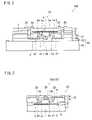
- FIG. 3is a cross-sectional view illustrating a schematic structure of a semiconductor element which is transferred onto the semiconductor device of the embodiment of the present invention.
- FIG. 4are cross-sectional views illustrating steps of forming on a semiconductor substrate the semiconductor element which is transferred onto the semiconductor device of the embodiment of the present invention.
- FIG. 5is a cross-sectional view illustrating a method for alignment when transferring the semiconductor element onto a TFT substrate.
- FIG. 6is a cross-sectional view illustrating a schematic structure of the semiconductor device such that a monocrystalline Si semiconductor element and a non-monocrystalline Si semiconductor element co-exist on the TFT substrate.
- a semiconductor device of the present inventionis a semiconductor device utilizing an insulating substrate having a low heat resistance as a substrate onto which a semiconductor element such as a semiconductor transistor is finally transferred (moved), namely, as a substrate which is finally used for, for example, a display apparatus and is a so-called production substrate.
- the insulating substrateis a substrate such as a glass substrate and has been conventionally difficult to apply.
- the semiconductor device of the present embodimentis a semiconductor device having a structure in which a chip-type semiconductor transistor, which is the semiconductor element above, has been transferred onto a substrate formed (TFT substrate) on which a pixel area has been formed.
- the semiconductor deviceis preferably arranged such that a MOS non-monocrystalline silicon thin film transistor (non-monocrystalline Si semiconductor element) and a MOS monocrystalline silicon thin film transistor (monocrystalline Si semiconductor element) are each formed in different regions on an insulating substrate 81 such as a glass substrate.
- the semiconductor deviceis suitable for realizing higher performance/functionality.
- a MOS semiconductor transistorhas an active semiconductor layer, a gate electrode (gate), a gate insulating film, and high-concentration impurity doping sections (source/drain) formed on the both sides of the gate.
- the MOS semiconductor transistoris a general transistor such that a carrier concentration in a semiconductor layer under the gate is adjusted by the gate, whereby an electric current between the source and the drain is controlled.
- Such a MOS transistoris suitable for a low-power consumption logic because, when the MOS transistor has a CMOS (Complementary MOS) structure, the MOS transistor consumes less power and a high output can be obtained therefrom in accordance with a supply voltage.
- CMOSComplementary MOS
- the MOS transistorpreferably has a CMOS (Complementary MOS) structure.
- CMOSComplementary MOS
- MOSMetal Oxide Semiconductor
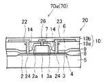
- a semiconductor device 100 of the present embodimentincludes on a TFT substrate 80 a MOS transistor 70 (hereafter, simply referred to as “transistor”) which has been made into a chip, a protective insulating film 91 , a metal wiring layer 92 , etc.
- the TFT substrate 80has a structure such that a wiring layer 82 is provided on the insulating substrate 81 .
- the transistor 70includes a monocrystalline Si (silicon) wafer (hereafter, referred to as “monocrystalline Si wafer”) 5 which is a monocrystalline Si substrate including an active layer 4 , a gate insulating film 6 formed on the monocrystalline Si wafer 5 , a gate electrode 7 (gate) formed on the gate insulating film 6 , a source electrode 22 and a drain electrode 23 connected to the source region 2 and the drain region 3 respectively, a LOCOS (Local Oxidation of Silicon) film 8 (field oxide film) whose film thickness is thicker than the gate insulating film 6 which LOCOS film 8 is formed on the monocrystalline Si wafer 5 around the active layer 4 , an NSG (Non-doped Silicate Grass) film 9 which is an oxide film formed on the gate electrode 7 and the LOCOS film 8 , and a silicon dioxide (SiO 2 ) film (hereafter, referred to as “TEOS film”) which is an oxide film 10 which
- TEOS filmsilicon dioxide
- the active layer 4has shallow element regions in which reverse conducting dopant is doped.
- the element regionsrespectively have a section in which N + or P + dopant is doped, which section is the source region 2 or the drain region 3 .
- the transistor 70 of the present embodimenthas an LLD (Lightly doped drain) structure, in which the monocrystalline Si wafer 5 is fabricated as follows: The channel region 1 is formed under the gate electrode 7 . Low-concentration impurity regions 2 a and 3 a are formed in regions adjacent to the channel region 1 . In outer regions of the low-concentration impurity regions 2 a and 3 a , the source region 2 and the drain region 3 are formed which are connected to the source electrode 22 and the drain electrode 23 , respectively. Note that the LLD structure is not essential in the present invention.
- the NSG film 9(oxide film) is formed by CVD (chemical vapor deposition) so as to cover all the top surfaces of the gate insulating film 6 and the gate electrode 7 .
- the surface of the planarized oxide film 10is planarized through, for example, a CMP (Chemical Mechanical Polishing) process etc.
- the LOCOS film 8is a film formed as a device separation region.
- the LOCOS film 8can be formed by LOCOS method.
- the LOCOS film 8is thus formed as a thick thermally-oxidized film (field oxide film) around the active layer 4 .
- the source electrode 22 and the drain electrode 23are respectively connected to the source region 2 and the drain region 3 through contact holes 24 which are the connecting holes formed through the gate insulating film 6 and the NSG film 9 .
- the protective insulating film 91is formed on the active layer 4 and the LOCOS film 8 .
- the metal wiring layers 92are formed so as to be respectively connected to the source electrode 22 and the drain electrode 23 through contact holes 25 which are the connecting holes formed through the protective insulating film 91 , the LOCOS film 8 , and the NSG film 9 .
- the metal wiring layers 92are used as, for example, a source wiring and a drain wiring.
- a contact hole not illustrated in FIG. 2i.e., another contact hole 25 not illustrated in FIG. 2
- the contact hole not illustratedis a connecting hole formed through the protective insulating film 91 , the LOCOS film 8 , and the NSG film 9 .
- a metal wiring layer not illustrated in FIG. 2i.e., another metal wiring layer 92 not illustrated in FIG. 2
- the metal wiring layer not illustratedis connected to the gate electrode 7 (gate) through a contact hole 26 which is a connecting hole formed in an area of the NSG film 9 which area is opposite to the gate electrode 7 (gate).
- the active layer 4 of the transistor 70is a semiconductor.
- the active layer 4is not especially limited to a specific material as long as the active layer 4 is a semiconductor.
- the active layer 4is a semiconductor of polycrystalline, monocrystalline, or the like composed of Si, Ge, GaAs, GaP, CdS, CdSe, or the like.
- the planarized oxide film 10is not limited to the TEOS film, but may be an SiO 2 film, a phosphorus silicate glass (PSG) film, a boron phosphorus silicate glass (BPSG), or the like.
- PSGphosphorus silicate glass
- BPSGboron phosphorus silicate glass
- the semiconductor device 100can include both a MOS non-monocrystalline silicon thin film transistor (non-monocrystalline Si semiconductor element) and a MOS monocrystalline silicon thin film transistor (monocrystalline Si semiconductor element) on the insulating substrate 81 , namely, on one TFT substrate 80 .
- a distance between a region for forming the non-monocrystalline Si semiconductor element and a region for forming the monocrystalline Si semiconductor elementis at least 0.3 ⁇ m or more, or preferably 0.5 ⁇ m or more. This can prevent metal atoms such as Ni, Pt, Sn, and Pd from diffusing in the monocrystalline Si semiconductor element. As a result, stable properties of the monocrystalline Si semiconductor element can be attained.
- the semiconductor device 100 of the present embodimentpreferably includes an SiO 2 film which is an interlayer insulating film between the non-monocrystalline Si semiconductor element and the monocrystalline Si semiconductor element. This makes it possible prevents contamination of the monocrystalline Si thin film semiconductor element.
- the semiconductor device 100further includes SiNx (silicon nitride), a planarized resin film, a via hole, and a transparent electrode so as to allow liquid crystal display operation.
- SiNxsilicon nitride
- a driver and a TFT for a display sectionare formed in the region for forming the non-monocrystalline Si semiconductor element.
- a timing controlleris formed in the region for forming the monocrystalline Si semiconductor element which is adaptive to a device required to have higher performance.
- a driver sectionmay be a monocrystalline Si semiconductor element. This may be determined in consideration of cost and performance.
- the TFT substrate 80 onto which the transistor 70 is bondedis a substrate for mounting a transistor thereon which substrate is made by forming the wiring layer 82 on the insulating substrate 81 .
- the TFT substrate 80is referred to as production substrate (hereafter, referred to as “substrate (B)”).
- substrate (B)production substrate
- the TFT substrate 80is, for example, a circuit substrate having a pixel area etc. or the like. Such a circuit substrate is used for an active-matrix display apparatus.
- the insulating substrate 81 used for the TFT substrate 80is a substrate such as a glass substrate, a plastic substrate, a so-called thin film, a so-called metal film, and the like. These substrates have been difficult to use for the manufacture of devices because the substrates generally have a low heat resistance.
- the insulating substrate 81itself may have insulation properties.
- the insulating substrate 81may have a structure such that an insulating layer is provided on a substrate as a base. Thickness of the insulating substrate 81 is not especially limited, but may be set according to a material of a substrate, purpose of use, etc.
- the insulating substrate 81is not especially limited, but, specifically, in the application of the present invention, the insulating substrate 81 is preferably a substrate whose upper temperature limit is less than 700° C. On the surface of the insulating substrate 81 , patterns such as wiring patterns are formed.
- an upper temperature limit of a glass substratemeans a strain point.
- the plastic substrateis not especially limited, but is a polyethersulfone substrate etc., for example.
- the plastic substratepreferably has light transmission properties. More preferably, the plastic substrate is a transparent plastic substrate.
- the thin film abovehas flexibility so as to fold, bend, and/or freely change the shape thereof and does not crash when dropped.
- a general-purpose thin filmsuch as an organic film can be used here.
- the metal film aboveis non-transparent and electrically conductive.
- an example of the metal filmis a stainless film.
- a layer having insulation properties, such as SiO 2is provided on the surface of the metal film.
- the semiconductor device 100 thus obtainedcan be suitably applied to, for example, a liquid crystal display apparatus.
- the insulating substrate 81(transparent substrate) made a material having light transmission properties such as a glass substrate has high light transmission properties. Therefore, the insulating substrate 81 can be suitably applied to, for example, a liquid crystal display apparatus. On the other hand, the insulating substrate 81 has a low strain point. As a result, it has been conventionally difficult to form a semiconductor device 100 having a low S coefficient (subthreshold coefficient).
- the present embodimentit is possible to provide a semiconductor device 100 having a low S coefficient, the semiconductor element 100 having a transistor 70 , whose performance is higher than ever, on the insulating substrate 81 thus having a low heat resistance.
- the insulating substrate 81 of the present embodimentis preferably a glass substrate or a plastic substrate.
- the followingdescribes a method for manufacturing the semiconductor device 100 of the present embodiment, with reference to (a) to (n) of FIG. 1 , FIGS. 2 , 3 , (a) to (f) of FIG. 4 , and FIG. 5 .
- the followingdescribes the formation of a monocrystalline Si thin film transistor 70 a illustrated in FIG. 3 , which is equivalent to the transistor 70 .
- the present inventionis not limited to the description.
- the followingalso describes in detail the method for manufacturing the semiconductor device 100 , showing concrete numeric values used in the manufacture of the semiconductor device 100 .
- the present inventionis not limited to concrete examples below.
- a device substrateis made by building the monocrystalline Si thin film transistor 70 a as the transistor 70 onto a semiconductor substrate (wafer) which is a base substrate, specifically onto the monocrystalline Si wafer 5 (monocrystalline Si substrate).
- the monocrystalline Si thin film transistor 70 a thus formed on the device substrateis transferred at least twice from the device substrate to a temporary supporting substrate and is made into a chip.
- the monocrystalline Si thin film transistor 70 ais transferred onto the TFT substrate 80 which is a production substrate on which the monocrystalline Si thin film transistor 70 a is finally mounted. It should be noted that the present invention is not limited to this example.
- the monocrystalline Si thin film transistor 70 a of the present embodimentis formed on the monocrystalline Si wafer 5 before being bonded onto the TFT substrate 80 . After being made into a chip, the monocrystalline Si thin film transistor 70 a is bonded onto the TFT substrate 80 . It is easier to perform the microfabrication of a monocrystalline Si thin film when performing on the monocrystalline Si wafer 5 the formation of the gate electrode 7 and the dopant ion doping for forming a source/drain, than when performing the formation of the monocrystalline Si thin film transistor 70 a after forming a monocrystalline Si thin film on the insulating substrate 81 of the TFT substrate 80 .
- a substrate used for a device substrate 20 as illustrated in FIG. 3 and (a) to (f) of FIG. 4(hereafter, the substrate is referred to as “semiconductor substrate (A)”), in other words, a base substrate (wafer) to form a transistor is not especially limited to a specific substrate as long as the substrate can be used for the formation of the transistor.
- such a base substrateis an Si substrate such as a monocrystalline Si wafer (monocrystalline Si substrate), a GaAs substrate, or the like.
- a size of a wafer (base substrate), the wafer used for the device substrate,is not especially limited, but, a large diameter is preferable because more transistors can be formed and therefore the cost of manufacturing the device substrate 20 and, moreover, the cost of manufacturing the semiconductor device 100 can be reduced.
- the monocrystalline Si wafer 5is used as the base substrate.
- a miniaturized transistoris formed on the monocrystalline Si wafer 5 so as to form that monocrystalline Si substrate as the device substrate 20 on which a part to be made into the transistor 70 , namely, the monocrystalline Si thin film transistor is built.
- the device substrate 20 of the present embodimentcan be made through, for example, a common Si process.
- a size of a waferis set to 6 inches (approximately 15 cm).
- the miniaturized transistoris formed on the whole surface of the wafer.
- the monocrystalline Si wafer 5 made of monocrystalline siliconis prepared and the surface thereof is oxidized so as to form a shallow SiO 2 (silicon dioxide) film 11 , whose thickness is approximately 30 nm.
- an SiN (silicon nitride) film 12is deposited on the whole SiO 2 film 11 by plasma CVD (Chemical Vapor Deposition).
- the SiN film 12is etched so that a part not to be an element region is etched away and while a part to be the element region is left.
- an oxide film made of SiO 2is developed as a field oxide film by, for example, dry oxidation. Thereby, for example, a LOCOS film 8 of 400 nm thick is formed.
- the SiN film 12is removed by etching.
- boron (B) ions or phosphorus (P) ionsare doped into an element region 13 surrounded by the LOCOS film 8 , then, the SiO 2 film 11 is removed by etching.
- a P-type regionis formed by doping boron ions into the element region 13 .
- boron ionsBy doping arsenic (As) ions into the P-type region so as to form the source region 2 and the drain region 3 , a N-type MOS transistor is formed.
- an N-type regionis formed by doping phosphorus ions into the element region 13 .
- boron fluoride ionsBy doping boron fluoride ions into the N-type region so as to form the source region 2 and the drain region 3 , a P-type MOS transistor is formed.
- the N-type MOS transistor and the P-type MOS transistorcan be formed simultaneously. Therefore, after forming the N-type MOS transistor and the P-type MOS transistor, a CMOS transistor can be obtained.
- the active layer 4is a region including the channel region 1 under the gate electrode 7 , the source region 2 , and the drain region 3 .
- impurity ions for adjusting threshold voltageis doped into the channel region 1 under the gate electrode 7 .
- SiO 2 having a thickness of 15 nmis developed as the gate insulating film 6 by, for example, dry oxidation.
- the gate insulating film 6 and the LOCOS film 8can be formed by also a thermal oxidation method such as a pyrogenic oxidation method or an HCl (hydrogen chloride) oxidation method.
- a thickness of the gate insulating film 6is not especially limited to a specific thickness, but is generally set in a range of 3 nm to 200 nm.
- a thickness of the LOCOS film 8is set, for example, to be not less than 250 nm but not more than 2000 nm.
- a polycrystalline silicon (hereafter, referred to as “p-Si”) film approximately 300 nm thickis deposited on the gate insulating film 6 .
- Phosphorous oxychloride (POCl 3 ) not illustrated in figuresis also deposited on the gate insulating film 6 .
- diffusionis performed at a temperature of 800° C.
- Patterning of the gate electrode 7is performed.
- boron ions or phosphorous ionsare doped to the areas which are formed into the low-concentration impurity regions 2 a and 3 a .
- SiO 2is deposited thereon up to a thickness in a range of 200 nm to 2000 nm (in the present embodiment, approximately 300 nm).
- Side walls 14 and 14are formed by etch back of Reactive Ion Etching (RIE; Reactive Ion etching).
- RIEReactive Ion Etching
- arsenic ions or boron fluoride ionsare doped to the areas which are formed into source/drain regions.
- Activation annealingis then performed at the temperature of approximately 900° C.
- the NSG film 9 having a thickness of 150 nmis developed by a CVD method. Furthermore, an SiO 2 film to be a planarized oxide film 10 a (first planarized oxide film), the SiO 2 film having a thickness of 1 ⁇ m is formed from the TEOS on the surface of the NSG film 9 by a method of PCVD (Plasma enhanced Chemical Vapor Deposition: plasma CVD).
- PCVDPulsma enhanced Chemical Vapor Deposition: plasma CVD
- the surface of the SiO 2 film(hereafter, referred to as “TEOS film”), which SiO 2 film is to be the planarized oxide film 10 a , is etched to a depth of 500 nm or more by a CMP method, so as to planarize the surface.
- the surface of the TEOS filmis etched to a depth of 200 nm by CMP.
- formedis that monocrystalline Si wafer 5 whose surface has been planarized as illustrated in FIG. 3 , onto which the monocrystalline Si thin film transistor 70 a has been built.
- ions for cleaving the monocrystalline Si wafer 5are doped therein from above the planarized oxide film 10 .
- an ion doping layer 15is formed on the monocrystalline Si wafer 5 .
- the ions for cleavingmay be conventional ions for cleaving a substrate, which are used in the Smart-Cut® method.
- Such ionsare, for example, noble gas ions and the like, the noble gas ions such as hydrogen ions and helium ions.
- conditions for doping ionsthe ions for cleaving a substrate
- conventional conditions for ion dopingconditions for cleavage
- the conditions for doping ionsare not especially limited, but are set according to types etc. of ions.
- hydrogen ionsare used for causing the cleavage.
- Conditions for doping the hydrogen ionsare a doping acceleration voltage of 150 KeV and a doping (dose) amount of 5 ⁇ 10 16 /cm 2 .
- the doping acceleration voltageis for determining a cleaving position.
- the doping acceleration voltageis changed according to conditions required for a transistor.
- the doping amountis for causing the cleavage.
- a small doping amountdoes not cause a cleavage. Therefore, the doping amount need to be set in a range of 1 ⁇ 10 15 /cm 2 to 1 ⁇ 10 17 /cm 2 .
- a doping energyis adjusted so that the ion doping layer 15 in the active layer 4 made of monocrystalline silicon deepens into an Si crystal of a lower part of the LOCOS film 8 .
- the contact holes 24 / 24 and the contact hole 26are formed.
- a metal electrode materialthereon, a contact and a metal film are formed.
- the source electrode 22 and the drain electrode 23are formed by etching etc. in a common Si transistor formation process.
- a TEOS film having a thickness of 2 ⁇ mis formed. The surface of the TEOS film is shaved off 1 ⁇ m so as to form a TEOS film as the planarized oxide film 10 b (second planarized oxide film).
- a TEOS filmbe formed in a large thickness and then polished down the thickness largely because this provides a better flatness Rms of the surface of a substrate and reduces waviness of the surface of the substrate.
- a time for polishingbecomes long. Therefore, it is preferable to select an appropriate thickness of the TEOS film in order to avoid polishing of too long time.
- a thickness of the TEOS filmis preferably in a range of 1.0 ⁇ m to 3 ⁇ m.
- a substrate on which the transistor 70(the monocrystalline Si thin film transistor 70 a ) is formed is generically referred to as “transistor substrate,” regardless of whether or not the transistor 70 , which is the monocrystalline Si thin film transistor 70 a here, is built right onto the monocrystalline Si wafer 5 or is held by the monocrystalline Si wafer 5 after transfer.
- the device substrate 20is formed through the steps described above, which are illustrated in (a) to (f) of FIG. 4 whereas the first temporary supporting substrate 30 is prepared as illustrated in (b) of FIG. 1 .
- the first temporary supporting substrate 30is a substrate for improving characteristics of the transistor 70 (the monocrystalline Si thin film transistor 70 a ) in such a manner that, the transistor 70 (which is the monocrystalline Si thin film transistor 70 a here) built right onto the device substrate 20 , which is a transistor substrate, is temporarily transferred to the first temporary supporting substrate 30 and the first temporary supporting substrate 30 is heat-treated, thereby repairing a crystal defect in a transistor channel on the device substrate 20 (i.e., a crystal defect in a transistor channel of the transistor 70 ).
- temporary supporting substrate (C)such a substrate is referred to as “temporary supporting substrate (C).
- repairing a crystal defectmeans to reduce crystal defects in a transistor channel of the transistor 70 (semiconductor element). Although a decrease in crystal defects in a transistor channel can be found by observation, the decrease can be also found from raised mobility of an obtained semiconductor transistor, a decreased leak current, a decrease in an S (Subthreshold) value, or the like. In the present embodiment, a crystal defect is most preferably repaired to the extent that transistor characteristics which are obtained from a nondefective monocrystalline Si can be obtained.
- a temperature for repairing a crystal defectmeans a temperature at which crystal defects in the transistor channel can be reduced.
- the first temporary supporting substrate 30used as the first temporary supporting substrate 30 is a substrate which does not suffer from a plastic deformation in a heat treatment for repairing the crystal defects.
- an upper temperature limit of a heat treatmentis a temperature at which an impurity doping profile does not change, there is a limit in actuality. Therefore, there is no specific temperature for an upper temperature limit of a heat treatment, as long as the first temporary supporting substrate 30 does not suffer from a plastic deformation at a heat treatment temperature for repairing the crystal defect.
- the first temporary supporting substrate 30can be specifically a monocrystalline Si substrate, for example, but is not limited to a specific substrate as long as the conditions above are satisfied.
- an Si substratesuch as a monocrystalline Si substrate is suitable for the first temporary supporting substrate 30 because the Si substrate has a high heat resistance and is easily available.
- the first temporary supporting substrate 30When using an Si substrate such as a monocrystalline Si substrate as the first temporary supporting substrate 30 , it is preferable in a viewpoint of adhesion energy that, by performing a thermal oxidation on the surface of the Si substrate after a cleaning of the surface, a thermally-oxidized film is formed on the surface.
- the thermally-oxidized filmhas a high adhesion energy. Therefore, by forming the thermally-oxidized film, adherability can be improved. Accordingly, a thickness of the thermally-oxidized film is not especially limited, but is preferable in a range of 30 nm to 300 nm from a view point of a time for film formation.
- a method for the cleaningis not especially limited, but a normal method can be employed.
- a cleaning method with SC1 and the likeare employed.
- the thermally-oxidized filmcan be easily formed by heat-treating the surface of the Si substrate at a temperature in a range of 1000 to 1200° C.
- the first temporary supporting substrate 30is a substrate onto which the monocrystalline Si thin film transistor 70 a built on the device substrate 20 is temporarily transferred. Therefore, the first temporary supporting substrate 30 is stripped after characteristic improvement of the monocrystalline Si thin film transistor 70 a . Therefore, a surface size of the first temporary supporting substrate 30 and a thickness thereof are not especially limited as long as the first temporary supporting substrate 30 can support the monocrystalline Si thin film transistor 70 a built on the device substrate 20 .
- the first temporary supporting substrate 30should have at least the same size of the monocrystalline Si thin film transistor 70 a built on the device substrate 20 .
- the first temporary supporting substrate 30may have the same size of the device substrate 20 or may have a larger size than the device substrate 20 .
- a substrate as the first temporary supporting substrate 30is prepared in such a way that, after cleaning the surface of a monocrystalline Si wafer 31 (monocrystalline Si substrate), which has the same size as the device substrate 20 (i.e., the monocrystalline Si wafer 5 on which the monocrystalline Si thin film transistor 70 a is formed), the monocrystalline Si wafer 31 is thermally oxidized in an oxidation furnace at 1100° C. for 60 minutes, thereby forming on the surface of the monocrystalline Si wafer 31 (on a surface onto which a transistor is transferred) a thermally-oxidized film 32 having a thickness of 200 nm.
- each bonding surfaceis cleaned with an SC1 solution so as to be activated and is washed with water.
- both substratesare bonded to each other while both substrates being appressed against each other at a room temperature.
- the first temporary supporting substrate 30 and the device substrate 20spontaneously bond to each other by bring both substrates into contact with each other and pressing both substrates with a small force. That is, bonding of both substrates is realized without an adhesive, due to a contribution of Van der Waals' force, a contribution of an electric dipole, and a contribution of hydrogen bonding.
- the bondingis easily realized between substrates such that each bonding surface thereof has a close proportion of the three contributions above to each other. Therefore, cleanness of the surfaces of the substrates and a degree of activity are very important for bonding both substrates without an adhesive.
- both substratesare preferably dried after being cleaned with an SC1 solution.
- the monocrystalline Si thin film transistor 70 ais bonded onto the first temporary supporting substrate 30 , with an inorganic insulating film sandwiched inbetween.
- the monocrystalline Si wafer 5is cleaved and separated, so that a cleaved surface may be the ion doping part 15 (a projection range of hydrogen ion doping).
- both substratesare heat-treated by RTA (Rapid Thermal Annealing) for 10 minutes.
- RTARapid Thermal Annealing
- an unnecessary part 5 a of the monocrystalline Si wafer 5 of the device substrate 20is cleaved and stripped along the ion doping layer 15 by the so-called Smart-Cut® method.
- a transferring layer including the monocrystalline Si thin film transistor 70 ais separated from the device substrate 20 (first transferring step).
- the RTA processis preferably performed at a temperature at which hydrogen surely dissipates from the device substrate 20 or more, specifically at a temperature in a range of 600 to 700° C.
- both substratesare further tightly bonded to each other due to an atomic bond.
- the stripped surface of the monocrystalline Si wafer 5 on the side of a transistor substrate 40i.e., the surface of a thermally-oxidized film 5 b
- the transistor substrate 40 obtained through the step aboveis etched so that the monocrystalline Si wafer 5 remained on the surface of the monocrystalline Si thin film transistor 70 a may have a desired thickness.
- the transistor substrate 40is heat-treated at a high heat, thereby repairing a crystal defect in the transistor channel in order to improve characteristics of the monocrystalline Si thin film transistor 70 a.
- a crystal defect in the transistor channelcan be repaired by heat-treating the transistor substrate 40 at a temperature in a range of 700° C. to an upper temperature limit of the first temporary supporting substrate 30 .
- the temperatureis in a range of 700 to 1400° C., more preferably in a range of 700 to 1200° C., or especially more preferably in a range of 700 to 900° C.
- a temperature for the heat treatmentdepends on varieties of the base substrate of the device substrate 20 .
- the heat treatmentis basically set to such a temperature range and process condition that impurity doping profiles of the source/drain/channel of does not change. This is because, if the impurity doping profiles of the source/drain/channel change, this may result in a change in the characteristics of the transistor 70 (which is the monocrystalline Si thin film transistor 70 a here).
- a time for the heat treatmentis not especially limited, but can be set according to a temperature for the heat treatment.
- the time for the heat treatmentis preferably set to a time in a range such that the impurity doping profiles do not change. Therefore, the temperature for the heat treatment is preferably shorter as long as the same characteristics can be obtained. The higher the temperature for the heat treatment, the shorter the time for the heat treatment to obtain the same effect. Accordingly, the time for the heat treatment depends on the temperature for the heat treatment, but is set in a range of, for example, one minute to two hours, approximately. However, the time for the heat treatment can be changed according to the temperature for the heat treatment.
- the transistor substrate 40is heat-treated, specifically, at 850° C. for one hour, in order to improve characteristics of a transistor (crystal defect repairing step).
- a TEOS film 41 having a thickness of 2 ⁇ mis formed on the monocrystalline Si thin film transistor 70 a of the transistor substrate 40 and the surface of the TEOS film 41 is etched to a depth of 1.2 ⁇ m by CMP method so as to planarize the surface.
- a second temporary supporting substrate 50is prepared.
- the second temporary supporting substrate 50is a substrate onto which the monocrystalline Si thin film transistor 70 a is temporarily transferred (hereafter, referred to as “temporary supporting substrate (D)”), in order to strip the first temporary supporting substrate 30 from the transistor substrate 40 , whose transistor has been improved in its characteristics, before transferring the monocrystalline Si thin film transistor 70 a onto the TFT substrate 80 , which is a production substrate.
- temporary supporting substrate (D)a substrate onto which the monocrystalline Si thin film transistor 70 a is temporarily transferred
- the first temporary supporting substrate 30is also unnecessary for the complete semiconductor device 100 as well as the base substrate of the device substrate 20 , it is necessary to remove the first temporary supporting substrate 30 .
- the first temporary supporting substrate 30is tightly bonded, by the heat treatment at a high heat in the crystal defect repairing step, onto the transistor substrate 40 , namely, the device substrate 20 such that the monocrystalline Si wafer 5 has been removed by cleaving along the ion doping layer 15 .
- the first temporary supporting substrate 30is transferred onto the TFT substrate 80 which is a production substrate and removed by cleavage caused by ion doping, namely, by the so-called Smart-Cut® method
- crystal defectsare generated in the transistor channel of the TFT substrate 80 .
- transistor characteristicsare degraded. Therefore, it is meaningless to transfer the device substrate 20 onto the first temporary supporting substrate 30 instead of the TFT substrate 80 .
- the monocrystalline Si thin film transistor 70 awhich has been transferred onto the first temporary supporting substrate 30 , can be transferred onto the TFT substrate 80 by stripping the first temporary supporting substrate 30 from an adhesive layer after directly bonding the first temporary supporting substrate 30 onto the TFT substrate 80 , which is a production substrate.
- the former methodis difficult to employ because there is no conventionally known adhesive which has a high heat resistance to the extent to which the heat treatment at a high heat for repairing the crystal defects can be performed, moderate fragility, and the like, so that easy stripping and temporary bonding can be performed.
- the wiring layer 82 formed on the TFT substrate 80can be damaged depending on an etching method and a material for a wiring. For example, when an aluminum wiring is formed on the TFT substrate 80 , etching cannot be performed with an alkali.
- a wiring patternis formed after transferring the monocrystalline Si thin film transistor onto the insulating substrate 81 on which the wiring layer 82 has not been formed yet.
- the monocrystalline Si thin film transistor 70 awithout temporarily transferring the first temporary supporting substrate 30 onto the second temporary supporting substrate 50 in order to cleave and remove the first temporary supporting substrate 30 from the transistor substrate 40 , the monocrystalline Si thin film transistor 70 a , which is transferred onto the first temporary supporting substrate 30 , can be directly transferred onto the insulating substrate 81 .
- the semiconductor device 100may be manufactured in such a manner that, after the transistor 70 (monocrystalline Si thin film transistor 70 a ) built on the monocrystalline Si wafer 5 is temporarily transferred at least once onto a temporary supporting substrate (first temporary supporting substrate 30 ) other than the production substrate so as to repair crystal defects, the transistor 70 is made into a chip and is transferred onto the insulating substrate 81 , which is a production substrate to mount the transistor 70 thereon, thereafter forming the wiring layer 82 which has a wiring pattern.
- a temporary supporting substratefirst temporary supporting substrate 30
- an oxide film formed on the insulating substrate 81 by, for example, CVD (chemical vapor deposition)normally has some defects.
- CVDchemical vapor deposition
- the same problemarises when removing by etching an unnecessary base substrate of the device substrate 20 from the insulating substrate 81 .
- the first temporary supporting substrate 30is bonded onto the another temporary supporting substrate, namely, the second temporary supporting substrate 50 so as to transfer the monocrystalline Si thin film transistor 70 a onto the second temporary supporting substrate 50 and the first temporary supporting substrate 30 is stripped from the second temporary supporting substrate 50 , on which the monocrystalline Si thin film transistor 70 a is transferred, without directly bonding the first temporary supporting substrate 30 on which the monocrystalline Si thin film transistor 70 a has been transferred to the insulating substrate 81 which is a production substrate.
- the second temporary supporting substrate 50is a substrate onto which the monocrystalline Si thin film transistor 70 a is temporarily transferred in order to strip the first temporary supporting substrate 30 .
- a material thereofin other words, a type thereof is not especially limited as long as the type is not the same as that of the production substrate which is finally used and on which the wiring layer 82 is or has been formed.
- the same type of substrate as the first temporary supporting substrate 30can be used as the second temporary supporting substrate 50 .
- a substrate used for the second temporary supporting substrate 50is a substrate having a heat resistance in a range of 700° C. to 1400° C., or preferably, in a range of 800° C. to 1400° C.
- examples of the second temporary supporting substrate 50encompass a monocrystalline Si substrate etc.
- an Si substratesuch as a monocrystalline Si substrate is suitably used for the second temporary supporting substrate 50 because the Si substrate is easily available.
- the second temporary supporting substrate 50also merely holds the monocrystalline Si thin film transistor 70 a temporarily, as well as the first temporary supporting substrate 30 . Therefore, the second temporary supporting substrate 50 is eventually stripped and removed.
- the second temporary supporting substrate 50can be easily stripped and removed from the monocrystalline Si thin film transistor 70 a after transferring the monocrystalline Si thin film transistor 70 a onto the other substrate, for example, onto the TFT substrate 80 as a production substrate.
- a material of the second temporary supporting substrate 50is split by a weakened cohesion thereof caused by a compositional change of the material which compositional change is induced by heat, laser irradiation, or the like.
- a layer to be cleavedon the surface of the second temporary supporting substrate 50 , it is preferable to provide as a layer to be cleaved a layer which is split by a weakened cohesion thereof caused by a compositional change induced by heat, laser irradiation, or the like.
- the adhesive layermay be deposited onto the transistor substrate 40 .
- the second temporary supporting substrate 50does not require the heat treatment for repairing crystal defects at a high heat. Therefore, the second temporary supporting substrate 50 does not require as high heat resistance as the first temporary supporting substrate 30 has. Similarly, an adhesive for bonding the second temporary supporting substrate 50 with the transistor substrate 40 does not require as high heat resistance as an adhesive for bonding the first temporary supporting substrate 30 with the device substrate 20 which is a transistor substrate.
- a conventionally known adhesivecan be used as the adhesive for bonding the second temporary supporting substrate 50 with the transistor substrate.
- a material for the layer to be cleaved which is formed on the surface of the second temporary supporting substrate 50 or a material for the second temporary supporting substrate 50 which material is cleavableis not especially limited to a specific material as long as the material is split by a weakened cohesion thereof caused by a compositional change induced by an extraneous factor.
- Such materialsinclude hydrogenated amorphous silicon (a-SiH), in particular, a-SiH containing hydrogen in a range of 10 to 25% by weight, porous Si (porous silicon), and the like.
- the second temporary supporting substrate 50is also stripped as well as the first temporary supporting substrate 30 after transferring the monocrystalline Si thin film transistor 70 a onto another substrate, namely, the TFT substrate 80 in the present embodiment. Therefore, a surface size and a thickness are not especially limited as long as the monocrystalline Si thin film transistor 70 a can be supported. That is, as in the case of the first temporary supporting substrate 30 , the second temporary supporting substrate 50 may be also in the same size as the monocrystalline Si thin film transistor 70 a or in a size larger than the monocrystalline Si thin film transistor 70 a.
- a monocrystalline Si wafer 51(monocrystalline Si substrate) having the same size as the first temporary supporting substrate 30 is used for a base substrate as the second temporary supporting substrate 50 .
- An a-SiH (hydrogenated amorphous silicon) layer 52 containing hydrogen of 15% by weight and an SiO 2 layer 53are laminated in this order on the surface of the monocrystalline Si wafer 51 .
- a thickness of the a-SiH layer 52is 500 nm.
- a thickness of the SiO 2 layer 53is 2 ⁇ m.
- the a-SiH layer 52 and the SiO 2 layer 53are continuously formed by PCVD.
- the surface of the SiO 2 layer 53is planarized by etching to a depth of 1000 nm by CMP.
- the first temporary supporting substrate 30 on which the monocrystalline Si thin film transistor 70 a is transferred, and the second temporary supporting substrate 50are subjected to hydrophilic treatment in which a bonding surface of the first temporary supporting substrate 30 to the second temporary supporting substrate 50 and a bonding surface of the second temporary supporting substrate 50 to the first temporary supporting substrate 30 are activated by washing with, for example, an SC1 solution, and then washed with water so as to hydrophilize the bonding surfaces.
- the first temporary supporting substrate 30i.e., the transistor substrate 40
- the first temporary supporting substrate 30on which the monocrystalline Si thin film transistor 70 a has been transferred is bonded onto the second temporary supporting substrate 50 while both substrates being appressed against each other at a room temperature, in such a manner that the monocrystalline Si thin film transistor 70 a is sandwiched between the second temporary supporting substrate 50 and the first temporary supporting substrate 30 .
- the first temporary supporting substrate 30is removed by backgrinding until a thickness thereof is reduced to 100 ⁇ m or less. As illustrated in (i) of FIG. 1 , by wet-etching with TMAH (tetramethylammonium solution), a remaining part of the first temporary supporting substrate 30 is completely removed.
- TMAHtetramethylammonium solution
- the thermally-oxidized film 32 of the first temporary supporting substrate 30functions as an etching stopper.
- the surface of the oxidized filmis planarized by CMP, thereby obtaining a transistor substrate 60 .
- the transistor substrate 60namely, the monocrystalline Si thin film transistor 70 a transferred onto the second temporary supporting substrate 50 is split in a required chip size by dicing the second temporary supporting substrate 50 .
- a transistor substrate 60 athus made into a chip, which is a device chip (transistor chip) to be transferred.
- the TFT substrate 80 containing a pixel areais prepared as a production substrate on which the monocrystalline Si thin film transistor 70 a transferred onto the second temporary supporting substrate 50 is transferred.
- the TFT substrate 80used as the TFT substrate 80 is a substrate having on a glass substrate on which a panel is provided the pixel area and an area other than an area in which the device chip (transistor substrate 60 a ) is transferred. As illustrated in (l) of FIG. 1 , a size larger area is provided for a device transfer area in which the device chip is transferred, in consideration of a margin for transfer.
- each bonding surfaceis cleaned.
- the TFT substrate 80 and the transistor substrate 60 aare cleaned with, for example, SC1 and washed in water, thereby undergoing hydrophilic treatment. Then, each surface (transfer surface) of both the substrates is dried with a spin dryer etc.
- alignmentis performed between the transistor substrate 60 a and the TFT substrate 80 in accordance with an alignment mark 61 provided on the transistor substrate 60 a .
- the transistor substrate 60 ais bonded onto the TFT substrate 80 at a predetermined position on the TFT substrate 80 while both substrates being appressed against each other at a room temperature.
- FIG. 5illustrates an example such that the alignment mark 61 on the transistor substrate 60 a which is on an alignment stage 102 is detected by epi-illumination with a CCD camera 101 for alignment, which CCD camera is set in a microscope. A detection result is finally converted into an electric signal for processing.
- the alignment mark 61is formed on, for example, the LOCOS film 8 which is a field oxide film, using the same material as the gate electrode 7 .
- a substrate which can be used for the production substrateis a substrate made of an optically-transparent material such as a glass substrate which substrate is transparent for short-wavelength visible light and UV rays and whose surface does not diffuse light. Therefore, as the alignment marks 83 and 61 can be detected through the production substrate, that is, the glass substrate here. This makes it possible to perform more precise alignment.
- heat treatment by RTAis performed thereon so as to cause heat expansion (ablation) of hydrogen in the a-SiH layer 52 of the transistor substrate 60 a which has been transferred onto the TFT substrate 80 , thereby cleaving and removing an unnecessary part of the second temporary supporting substrate 50 from the a-SiH layer 52 as illustrated in (m) of FIG. 1 (final transfer step).
- treatment conditions for the RTA processare not limited to the concrete conditions described above as long as cleavage by ablation can be caused.
- a temperature for the RTA processis preferably in a range of 600 to 800° C. for the stability of an impurity profile.
- a time for the RTA processis set according to the temperature above and is not especially limited. However, performing a too long RTA process is not preferable for the stability of the impurity profile. Therefore, a time for the RTA process is set to, for example, approximately 2 to 20 minutes.
- the cleavagecan be also caused by the irradiation of an excimer laser (XeCl etc.).
- Sia-SiH layer 52 and SiO 2 layer 53 in the transfer area on the TFT substrate 80 is thinned by, for example, dry etching etc. Furthermore, as illustrated in FIG. 2 , the protective insulating film 91 is formed as an interlayer film.
- contact holes 25are formed through the protective insulating film 91 , the LOCOS film 8 , and the NSG film 9 .
- the metal wiring layers 92is formed in the contact holes 25 .
- Each of the metal wiring layers 92is connected to the source electrode 22 , the drain electrode 23 , and the gate electrode 7 .
- Each of the metal wiring layers 92 and the wiring layer 82 on the TFT substrate 80are connected (wiring connection process). In this way, the semiconductor device 100 of the present embodiment can be obtained.
- an organic insulating filmis further formed in a step for manufacturing a panel.
- a method for manufacturing a semiconductor device of the present embodimentrelates to a method such that, in order to transfer the transistor 70 (monocrystalline Si thin film transistor 70 a ) formed on a semiconductor substrate (A) such as the monocrystalline Si wafer 5 , more specifically, in order to transfer a transferring layer including the transistor 70 onto a substrate (B) (production substrate) on which the transistor 70 is finally transferred, hydrogen ions or noble gas ions are doped into the semiconductor substrate (A) so as to perform heat treatment thereon, thereby a part of the semiconductor substrate (A), that is, an unnecessary part except the transistor 70 being cleaved at the ion doping layer in order to remove the unnecessary part from the semiconductor substrate (A) on which the transistor 70 (monocrystalline Si thin film transistor 70 a ) is formed.
- a method for transferring a semiconductor element of the present embodimentin which method (I) from a semiconductor substrate (A) on which the semiconductor element is formed, a transferring layer including the semiconductor element is separated by doping hydrogen ions or noble gas ions in the semiconductor substrate (A), and then heat-treating the semiconductor substrate (A), so as to make a chip of the semiconductor element, and (II) the chip of the semiconductor element is transferred onto a substrate (B) on which the semiconductor element is finally mounted, the method includes: the ion doping step of doping hydrogen ions or noble gas ions in an interface of transferring layer of the semiconductor substrate (A) on which the semiconductor element is formed; the first transfer step of transferring the semiconductor element onto a temporary supporting substrate (C) in such a manner that the semiconductor substrate (A) on which the semiconductor element is formed is bonded onto the temporary supporting substrate (C) with the semiconductor element sandwiched therebetween and the semiconductor substrate (A) and temporary supporting substrate (C) thus bonded are heat-treated so as to separate the transferring layer to the
- the method for transferring the semiconductor element of the present embodimentis preferably as below. Hydrogen ions or noble gas ions are doped into a semiconductor substrate (A) so as to perform heat treatment thereon. A part (unnecessary part) of the semiconductor substrate (A) is stripped at the layer in which ions are doped from the semiconductor substrate (A) on which a semiconductor element is formed. The semiconductor element is finally transferred onto a substrate (B) whose upper temperature limit is lower than a temperature for repairing crystal defects, the crystal defects generated in a transistor channel of the semiconductor element by thus stripping.
- the semiconductor substrate (A) on which the semiconductor element has been formedhydrogen ions or noble gas ions are doped into the semiconductor substrate (A) on which the semiconductor element has been formed and the semiconductor substrate (A) is bonded onto a temporary supporting substrate (C), with the semiconductor element sandwiched therebetween.
- the temporary supporting substrate Chas heat resistance equal to or higher than a temperature for repairing crystal defects, the crystal defects generated in a transistor channel of the semiconductor element by thus stripping.
- heat treatinga part (unnecessary part) of the semiconductor substrate (A) is stripped from the layer in which ions are doped.
- the semiconductor elementis transferred onto the temporary supporting substrate (C).
- the temporary supporting substrate (C)is heat treated at a temperature equal to or higher than a temperature for repairing crystal defects, the crystal defects generated in the transistor channel of the semiconductor element so as to repair the crystal defects.
- the semiconductor elementis then made into a chip and transferred onto the substrate (B) by a different method from the method for transferring the semiconductor element utilizing ion doping.
- a method for transferring the semiconductor element of the present embodimentis preferably as below. Hydrogen ions or noble gas ions are doped into a semiconductor substrate (A) so as to perform heat treatment thereon. A part (unnecessary part) of the semiconductor substrate (A) is stripped at the layer in which ions are doped from the semiconductor substrate (A) on which a semiconductor element has been formed. The semiconductor element is finally transferred onto a substrate (B) whose upper temperature limit is lower than 700° C.
- the semiconductor substrate (A)is bonded onto a temporary supporting substrate (C), with the semiconductor element sandwiched therebetween.
- the temporary supporting substrate Chas an upper temperature limit equal to or higher than 700° C.
- the semiconductor elementis transferred onto the temporary supporting substrate (C).
- the temporary supporting substrate (C)is heat treated at a temperature in a range of 700° C. to the upper temperature limit of the temporary supporting substrate (C) so as to repair crystal defects generated in the transistor channel of the semiconductor element.
- the semiconductor elementis then made into a chip and transferred onto the substrate (B) by a different method from the method for transferring the semiconductor element utilizing ion doping.
- the transistor 70(monocrystalline Si thin film transistor 70 a ) built onto the semiconductor substrate (A) such as the monocrystalline Si wafer 5 onto the substrate (B) (production substrate) on which the transistor 70 is finally transferred, the transistor 70 is transferred onto a temporary supporting substrate at least once or preferably at least twice (i.e., at least onto the temporary supporting substrate (C) having high heat resistance, namely, the first temporary supporting substrate) so as to cleave and strip an unnecessary part 5 a (a part except the transistor 70 ) of the semiconductor element (A).
- a temporary supporting substrateat least once or preferably at least twice (i.e., at least onto the temporary supporting substrate (C) having high heat resistance, namely, the first temporary supporting substrate) so as to cleave and strip an unnecessary part 5 a (a part except the transistor 70 ) of the semiconductor element (A).
- the temporary supporting substrate (C) on which the transistor 70 has been transferredis heated at a temperature equal to or higher than a temperature for repairing crystal defects (i.e., 700 to 1200° C.) so as to repair crystal defects in the transistor channel after stripping the semiconductor substrate (A).
- the transistor 70is made into a chip and transferred onto the substrate (B) by a different method (i.e., a method except the Smart-Cut® method) from the method for stripping the unnecessary part 5 a of the semiconductor substrate (A).
- Different methods from the method for stripping the unnecessary part 5 a of the semiconductor substrate (A)include (I) a method utilizing etching, (II) a method utilizing an adhesive, (III) a method utilizing a layer (a) whose cohesion decreases due to compositional change induced by external factors such as heat and laser irradiation, the layer such as an a-SiH layer and a porous Si, (IV) combination of (I) to (III), and the like.
- the transistor 70is transferred onto the temporary supporting substrate (D) by removing the temporary supporting substrate (C) by etching and the temporary supporting substrate (D) is bonded onto the substrate (B) which is a production substrate, thereafter the temporary supporting substrate (D) being stripped from the layer (a) such as the a-SiH layer and the porous Si layer.
- the transistor 70is made into a chip before being transferred onto the substrate (B).
- the number of times that the transistor 70 is transferred onto the temporary supporting substrateis not especially limited. That is, as described above, as long as the transistor 70 built onto the semiconductor substrate (A) is temporarily transferred onto the temporary supporting substrate (C) having high heat resistance so as to repair crystal defects, the transistor 70 may be directly transferred from the temporary supporting substrate (C) to the substrate (B). Alternatively, the transistor 70 may be transferred from the temporary supporting substrate (C) to the temporary supporting substrate (D) further and then transferred onto the substrate (B). Moreover, the transistor 70 may be transferred from the temporary supporting substrate (D) to another temporary supporting substrate (D) and then transferred onto the substrate (B).
- a direction of the transistor 70i.e., a building direction of the gate electrode 7 to the active layer 4 ) can be adjusted (changed) depending on the number of transfers.
- the transistor 70is transferred onto the temporary supporting substrate (C) having high heat resistance so as to cleave and strip the unnecessary part 5 a of the semiconductor substrate (A). Then, the temporary supporting substrate (C) on which the transistor 70 has been transferred is heat treated at a temperature equal to or higher than a temperature for repairing crystal defects.
- a damaged layer having a crystal defect(lattice imperfection)
- the crystal defect made in the transistor channel after stripping an unnecessary part from the semiconductor substrate (A)is not merely removed, but the crystal defect itself (lattice imperfection) in the transistor channel can be repaired. This can fundamentally improve transistor characteristics affected by the crystal defect. Accordingly, the present invention can provide a semiconductor device having an S coefficient which is significantly lower than the conventional arts.
- an insulating substratewhich has low heat resistance and has been conventionally difficult to use can be used as a production substrate.
- transistor characteristicscan be improved.
- a semiconductor device having a low S coefficientcan be provided without an increase in manufacturing cost.
- the transfer methods abovecan be selected according to a type of the substrate (B), a type of a semiconductor element to be transferred onto the substrate (B), for example, a type of the transistor 70 , etc.
- the transfer method utilizing the layer (a) or the adhesivecan be employed as a transfer method which is different from the method used for stripping the unnecessary part 5 a of the semiconductor substrate (A).
- a glass substratesuch as a high-strain-point glass
- a semiconductor element made of amorphous siliconhereafter, referred to as “a-Si”
- the transfer method utilizing the layer (a) or the adhesiveas a transfer method for transferring the semiconductor element (A) onto the substrate (B) (i.e., a transfer method for the final transfer onto a production substrate) although etching utilizing an oxidized film can be used.
- the transfer method utilizing the layer (a) or the adhesiveis employed as a method for transferring the semiconductor element onto the substrate (B).
- the transistor 70 which is mounted (transferred) according to the method of the present invention on the TFT substrate 80has an S coefficient of 65 mV/decade or lower (i.e., S coefficient in a range of 60 (theoretical limitation) to 65 mV/decade). This is significantly low in contrast with a conventional S coefficient in a range of 90 to 100 mV/decade. This realizes excellent transistor characteristics which are considered to be impossibly difficult to realize utilizing a-Si or p-Si which is available currently or will be available a few years later.
- the transistor 70is an element that was transferred onto the TFT substrate 80 by the method above can be determined by measuring crystallinity of Si of the transferred transistor 70 .
- an area in which the transistor 70 is transferredbecomes monocrystalline by transferring crystal silicon onto the glass substrate whereas Si in an area in which the transistor 70 is not transferred is s-Si (strained silicon) or poly-Si. Therefore, it can be determined that the area in which the transistor 70 is transferred is monocrystalline because the area indicates a single direction such as (100) in, for example, Raman spectroscopic analysis or EBSP (Electron Back Scatter Diffraction Pattern).
- EBSPElectron Back Scatter Diffraction Pattern
- the semiconductor device 100 of the present embodimentcan be used in an area having a gate length of 0.25 ⁇ m, which is the half of a conventional gate length whereas a conventional semiconductor device can be used only in an area having a gate length of 0.5 ⁇ m and cannot be miniaturized further. This makes it possible to realize a device having a half area of a conventional device.
- the semiconductor device 100 of the present embodimentmay have on one substrate two types of transistors each having different characteristics from each other.
- the semiconductor device 100can be applied for various uses such as a display apparatus.
- the semiconductor device 100may be arranged such that a transferred transistor which has been transferred on a TFT substrate and a formed transistor which has been formed on the TFT substrate coexist on an insulating substrate which is a production substrate, namely, on the TFT substrate.
- the transistor 70namely, a transistor formed on the TFT substrate 80 by transfer is the monocrystalline Si thin film transistor 70 a .
- the transistor 70is not limited to the monocrystalline Si thin film transistor 70 a , but may be a transistor of a different type.
- the present embodimentdescribed a transistor, in particular, a thin film transistor including an active layer and a gate electrode as an example of a semiconductor element which is to be mounted (transferred) onto the semiconductor device 100 .
- the semiconductor device of the present inventionis not limited to such a transistor, but may be, for example, a driver, a memory, a thin film diode, etc. for driving an active-matrix circuit.
- the semiconductor device 100is suitably applicable to, for example, a peripheral driving circuit and a control circuit of a TFT-driven active-matrix liquid crystal display apparatus or a display apparatus such as an intelligent liquid crystal display apparatus such that an MPU (Micro Processing Unit) and an image processing circuit are packaged on one substrate and an OLED (Organic Light Emitting Diode: organic EL) display apparatus.
- a peripheral driving circuit and a control circuit of a TFT-driven active-matrix liquid crystal display apparatusor a display apparatus such as an intelligent liquid crystal display apparatus such that an MPU (Micro Processing Unit) and an image processing circuit are packaged on one substrate and an OLED (Organic Light Emitting Diode: organic EL) display apparatus.
- MPUMicro Processing Unit
- OLEDOrganic Light Emitting Diode: organic EL
- the TEOS filmwas used for an oxide film which is required to be planarized, such as the planarized oxide film 10 .
- the oxide filmsare not limited to this, but, as described above, an oxide film formed by the other film formation method such as an SiO 2 film formed by PCVD may be used instead of the TEOS film.
- an ion doping areacan have a flat shape.
- the planarized oxide film such as the TEOS filmis preferably formed on each bonding surface of substrates to be bonded to each other. This improves adherability of both substrates. Accordingly, both substrates can be bonded to each other, for example, without an adhesive.
- each bonding surfaceis preferably flat, clean, and dry (i.e., containing no moisture). Water molecules in a several molecular layer do not cause a problem.
- a flatness (Rms) of each bonding surfaceis preferably 0.5 nm or less, or, preferably 0.3 nm or less.
- a waviness size on each bonding surfaceis preferably 30 ⁇ m or less.
- the flatness (Rms)can be measured with an AFM (Atomic Force Microscope).
- the waviness sizecan be measured by surface roughness test with a contact stylus.
- a method for manufacturing a semiconductor deviceincludes a transferring step of transferring a semiconductor element onto a substrate (B) to be used in the semiconductor device by a transferring method for transferring the semiconductor device, in which transferring method (I) from a semiconductor substrate (A) on which the semiconductor element is formed, a transferring layer including the semiconductor element is separated by doping hydrogen ions or noble gas ions in the semiconductor substrate (A), and then heat-treating the semiconductor substrate (A), so as to make a chip of the semiconductor element, and (II) the chip of the semiconductor element is transferred onto a substrate (B) on which the semiconductor element is finally mounted, the transferring method including: the ion doping step of doping hydrogen ions or noble gas ions in an interface of transferring layer of the semiconductor substrate (A) on which the semiconductor element is formed; the first transfer step of transferring the semiconductor element onto a temporary supporting substrate (C) in such a manner that the semiconductor substrate (A) on which the semiconductor element is formed is bonded onto the temporary supporting substrate (C) with
- the method for manufacturing the semiconductor deviceis method including the step for transferring the semiconductor element onto the substrate (B) which is used in the semiconductor device, by the method for transferring the semiconductor element.
- the semiconductor deviceis fabricated by transferring by the method for transferring a semiconductor element, a chip of a semiconductor element onto the substrate (B) on which the semiconductor element is finally mounted, the semiconductor element being a semiconductor transistor and having an S coefficient of 65 mV/decade or less.
- the semiconductor element formed on the semiconductor substrate (A)is not directly transferred onto the substrate (B), but, before transferring the semiconductor element to the substrate (B), the semiconductor element is temporarily transferred onto the temporary supporting substrate (C), whose upper temperature limit is equal to or higher than a temperature for repairing a crystal defect, which is made in the transistor channel of the semiconductor element by the separation.
- the crystal defect, which is made in the transistor channel of the semiconductor element by the separationcan be repaired through heat treatment at the temperature for repairing a crystal defect or higher.
- the methodmakes it possible to prevent characteristic degradation of the semiconductor element inevitably caused by a crystal defect, which crystal defect is inevitably made in a transistor channel of the semiconductor element by separating a transferring layer (by stripping the unnecessary part of the semiconductor substrate (A)) in order to transfer the semiconductor element from the semiconductor substrate (A) on which the semiconductor element has been formed.
- a damaged layer having a crystal defect(lattice imperfection)
- the crystal defect made in the transistor channel after stripping the unnecessary part of the semiconductor substrate (A)is not removed, but crystal defects themselves (lattice imperfection) in the transistor channel can be repaired. This can fundamentally improve transistor characteristics affected by the crystal defect.
- the semiconductor device according to the present inventionhas better device characteristics than the conventional arts.
- the semiconductor deviceis suitably applicable to, for example, a peripheral driving circuit and a control circuit of a TFT-driven active-matrix liquid crystal display apparatus or a display apparatus such as an intelligent liquid crystal display apparatus such that an MPU and an image processing circuit are packaged on one substrate and an OLED display apparatus.
Landscapes
- Physics & Mathematics (AREA)
- Engineering & Computer Science (AREA)
- High Energy & Nuclear Physics (AREA)
- Condensed Matter Physics & Semiconductors (AREA)
- General Physics & Mathematics (AREA)
- Manufacturing & Machinery (AREA)
- Computer Hardware Design (AREA)
- Microelectronics & Electronic Packaging (AREA)
- Power Engineering (AREA)
- Health & Medical Sciences (AREA)
- Toxicology (AREA)
- Thin Film Transistor (AREA)
Abstract
Description
- The present invention relates to a method for transferring a semiconductor element, a method for manufacturing a semiconductor device, and the semiconductor device. More specifically, the present invention relates to (I) a method for transferring a semiconductor element, the method including forming a chip from a semiconductor element formed on a semiconductor substrate and transferring the semiconductor element onto a substrate (such as a glass substrate) having a low heat resistance, (II) a method for manufacturing a semiconductor device, the method utilizing the method for transferring a semiconductor element, and (III) a semiconductor device.
- As an art for forming a semiconductor element on an insulating substrate, the following art has been studied recently; a transistor (such as a semiconductor transistor) composed of a monocrystalline silicon thin film (hereafter, referred to as “monocrystalline Si thin film”) is formed on a semiconductor substrate in advance, then the transistor is bonded onto a (insulating) substrate on which the transistor is finally mounted, which substrate is a so-called production substrate and is a glass substrate etc., and the semiconductor substrate is then cleaved and stripped off to be separated from the transistor thereby attaining a thin film (see, for example,
Patent Documents - Especially, for the sake of easy microfabrication of monocrystalline silicon, a transistor composed of a monocrystalline silicon thin film (hereafter, referred to as “monocrystalline Si transistor”) is preferably formed by performing on a monocrystalline Si substrate (monocrystalline Si wafer) formation of a gate electrode and impurity ion doping for forming a source/drain, compared to performing the formation of the transistor after forming a monocrystalline Si thin film on a production substrate.
- The monocrystalline Si transistor is initially formed on a monocrystalline Si substrate. Then the monocrystalline Si transistor formed on the monocrystalline Si substrate is bonded onto the production substrate, in such a manner that the monocrystalline Si substrate is on the outer side. Then, the monocrystalline Si substrate is stripped off from the monocrystalline Si transistor. In this way, the monocrystalline Si transistor is transferred from the monocrystalline Si substrate onto the production substrate.
- As for a method for stripping the monocrystalline Si substrate off from the monocrystalline Si transistor bonded onto the production substrate, the so-called Smart-Cut® method is generally employed. According to the Smart-Cut method, doping a predetermined concentration of hydrogen ions or noble gas ions into the monocrystalline Si substrate causes microbubbles in a doping section of the monocrystalline Si substrate. The monocrystalline Si substrate is cleaved at a layer of the microbubbles, utilizing the layer as a cleaved surface (see
Patent Documents 1 and 2). - More specifically, after forming the monocrystalline Si transistor on the monocrystalline Si substrate, hydrogen ions are doped into the monocrystalline Si substrate, thereby forming a hydrogen ion doping layer with a predetermined depth from the surface of the monocrystalline Si substrate. Then, the monocrystalline Si substrate is bonded onto the production substrate and is heat-treated. As a result, the monocrystalline Si substrate is separated at the hydrogen ion doping layer, thereafter being stripped from the monocrystalline Si transistor.
- Japanese Unexamined Patent Publication No. 102848/1999 (Tokukaihei 11-102848, Publication date: Apr. 13, 1999)
Patent Document 1 corresponds to U.S. Pat. No. 6,140,210 (Registration date: Oct. 31, 2000).- Japanese Unexamined Patent Publication No. 2005-26472 (Tokukai 2005-26472, Publication date: Jan. 27, 2005)
- S. Utsunomiya et al., “Surface Free Technology by Laser Ablation/Annealing,” AM-LCD '02, pp. 37-40
- In the art such that ions for causing cleavage are doped and an unnecessary part is stripped at the ion doping layer from the monocrystalline Si substrate, the monocrystalline Si substrate after the cleaving-off of the unnecessary part has such problems that an area having a crystal defect (damaged area) is caused in a transistor channel of the monocrystalline Si substrate by lattice imperfection due to ion doping, unpaired electrons due to breaking a bond between Si atoms, and the like. Due to a defect that the monocrystalline Si transistor has an electric charge in such a damaged area, characteristics of the monocrystalline Si transistor are degraded. This leads to an increase in an S (subthreshold) coefficient (i.e., leads to a more gradual subthreshold slope).
- However, a strain point of a grass substrate, which is generally used as a production substrate, is approximately in a range of 600° C. to 650° C.
- Therefore, a glass substrate cannot be used as an insulating wafer in such a method as described in
Patent Document 1 in which, after bonding one Si wafer to another Si wafer having an ion doping layer or, alternatively, bonding an Si wafer having an ion doping layer to an insulating wafer and the Si wafer having an ion doping layer is cleaved by the Smart-Cut method, and before or after the cleaving, heat treatment is performed on the wafers in order to increase a bonding strength therebetween, thereby obtaining an SOI wafer, and a defective layer of the SOI wafer due to ion doping is removed by vapor-phase etching. - On the other hand, as described in
Patent Document 2, the applicants of the present invention take such measures that an oxide film is temporarily formed on the stripped surface and is then removed therefrom, thereby removing the damaged layer on the stripped surface. In order to form the oxide film, employed are high-pressure steam oxidation etc., in which a temperature of oxidation treatment is relatively low. This makes it possible to transfer a semiconductor element onto a glass substrate having a low strain point. - By employing the method, a glass substrate having a low strain point can be used as an article to which a semiconductor element is transferred, in other words, as a production substrate.
- However, the inventors of the present invention were not fully satisfied with the result above, but, in order to provide a semiconductor device having a semiconductor element of higher performance on an insulating substrate which has a low heat resistance, such as a glass substrate, the inventors diligently studied on how to prevent by a different method from that of
Patent Document 2 characteristic degradation of a semiconductor element caused by a crystal defect which is inevitably generated in a transistor channel of the semiconductor element when transferring the semiconductor element from a semiconductor substrate on which the semiconductor element is formed. - That is, in view of the problem, an object of the present invention is to provide (a) a method for transferring a semiconductor element which method makes it possible to prevent characteristic degradation of the semiconductor element inevitably caused by a crystal defect which is inevitably generated in a transistor channel of the semiconductor element by transferring the semiconductor element from a semiconductor substrate on which the semiconductor element is formed, (b) a method for manufacturing a semiconductor device, the method utilizing the method for transferring a semiconductor element, and (c) a semiconductor device.
- In order to solve the problem, a method for transferring a semiconductor element is a method, in which, from a semiconductor substrate (A) on which the semiconductor element is formed, a transferring layer including the semiconductor element is separated by doping hydrogen ions or noble gas ions in the semiconductor substrate (A), and then heat-treating the semiconductor substrate (A), so as to make a chip of the semiconductor element, and the chip of the semiconductor element is transferred onto a substrate (B) on which the semiconductor element is finally mounted, the method including: (i) the ion doping step of doping hydrogen ions or noble gas ions in an interface of transferring layer of the semiconductor substrate (A) on which the semiconductor element is formed; (ii) the first transfer step of transferring the semiconductor element onto a temporary supporting substrate (C) in such a manner that the semiconductor substrate (A) on which the semiconductor element is formed is bonded onto the temporary supporting substrate (C) with the semiconductor element sandwiched therebetween and the semiconductor substrate (A) and temporary supporting substrate (C) thus bonded are heat-treated so as to separate the transferring layer to the temporary supporting substrate (C) from the semiconductor substrate (A), the temporary supporting substrate (C) having an upper temperature limit equal to or higher than a temperature for repairing crystal defects generated in a transistor channel of the semiconductor element due to the separation (namely, due to, as described above, the separation, utilizing hydrogen ions or noble gas ions, of the transferring layer including the semiconductor element from the semiconductor substrate (A)); (iii) the crystal defect repairing step of repairing the crystal defects by heat-treating the temporary supporting substrate (C) on which the semiconductor element is transferred, at a temperature equal to or higher than the temperature for repairing crystal defects which are generated in the transistor channel of the semiconductor element; and (iv) the final transfer step of making the semiconductor element into the chip and transferring the chip of the semiconductor element onto the substrate (B) by a different method from the first transfer step.
- In other words, the method for transferring a semiconductor element is a method such that the semiconductor element formed on the semiconductor substrate (A), namely, the semiconductor element built on the semiconductor substrate (A) is made into a chip and is transferred onto the substrate (B) on which the semiconductor element is finally mounted. In the method for transferring a semiconductor element, the semiconductor element formed on the semiconductor substrate (A) is temporarily transferred onto the temporary supporting substrate (C). The temporary supporting substrate (C) is then heat-treated at a high heat so as to repair the crystal defect generated in the transistor channel of the semiconductor element when the semiconductor element is transferred onto the temporary supporting substrate (C). The semiconductor element is made into a chip, thereafter being transferred onto the substrate (B). The “transferring a semiconductor element” here means to move the semiconductor element from one substrate to the other substrate, in other words, to separate the semiconductor element from the one substrate and bond (mount) the semiconductor element onto the other substrate.
- As for re-transfer (i.e., re-separation and re-bond) of the semiconductor element separated from the semiconductor substrate (A) which has been used to form the semiconductor element, a different method from the described method utilizing ion doping for the separation (stripping an unnecessary part) can be employed as a method for separating the semiconductor element. Therefore, the different method from the first transfer step, namely, the transfer method utilizing ion doping is employed for the re-transfer of the semiconductor element which semiconductor element has been transferred from the semiconductor substrate (A) onto the temporary supporting substrate (C) and heat-treated so as to repair a crystal defect.
- There is no special limitation to a method such that the temporary supporting substrate (C) onto which the semiconductor element has been transferred is heat-treated so as to repair the crystal defect and the semiconductor element is made into a chip, thereafter being transferred onto the substrate (B) by a different method from the transfer method utilizing ion doping. A variety of conventional transfer methods can be employed as the method. In the method, for example, the following first to third methods can be preferably employed. The following methods can be used in combination.
- The first method includes, for example, after the steps between the first transfer step and the final transfer step, a re-transfer step of transferring the semiconductor element at least once onto a temporary supporting substrate (D) in such a manner that the temporary supporting substrate (C) is bonded onto the temporary supporting substrate (D) having a layer (a) made of hydrogenated amorphous silicon or porous silicon, with the semiconductor element sandwiched therebetween, and then the temporary supporting substrate (C) is removed by etching, the final transfer step including: making the chip with the semiconductor element and the temporary supporting substrate (D) on which the semiconductor element is transferred; bonding the chip onto the substrate (B) in such a manner that the temporary supporting substrate (D) is bonded onto the substrate (B) with the semiconductor element sandwiched therebetween; and removing the temporary supporting substrate (D) by heat-treating the layer (a) or by laser irradiation thereto, so as to transfer the chip of the semiconductor element onto the substrate (B).
- The second method includes, for example, after the steps between the first transfer step and the final transfer step, a re-transfer step of transferring the semiconductor element at least once onto a temporary supporting substrate (D) in such a manner that the temporary supporting substrate (C) is bonded onto the temporary supporting substrate (D) which is different from the temporary supporting substrate (C), with the semiconductor element sandwiched therebetween, and the temporary supporting substrate (C) is removed by etching, the final transfer step including: making the chip with the semiconductor element and the temporary supporting substrate (D) on which the semiconductor element is transferred; bonding the chip with the substrate (B) in such a manner that the temporary supporting substrate (D) is bonded onto the substrate (B) with the semiconductor element sandwiched therebetween; and removing the temporary supporting substrate (D) by etching, so as to transfer the chip of the semiconductor element onto the substrate (B).
- The third method is, for example, such that the final transfer step includes: making the chip with the semiconductor element and the temporary supporting substrate (C) on which the semiconductor element is transferred; bonding the chip with the substrate (B) in such a manner that the temporary supporting substrate (C) is bonded onto the substrate (B) with the semiconductor element sandwiched therebetween; and removing the temporary supporting substrate (C) by etching, so as to transferring the chip of the semiconductor element onto the substrate (B).
- In the crystal defect repairing step, a temperature of heat treatment is preferably 700° C. or higher and is especially preferably in a range of 700° C. to 900° C.
- The present invention is suitable for a case where an upper temperature limit of the substrate (B) is lower than a temperature for repairing a crystal defect generated in the transistor channel of the semiconductor element. As the substrate (B), for example, a glass substrate and a plastic substrate can be used.
- Also, the present invention is suitable for a case where the semiconductor element is a semiconductor transistor.
- According to the method for transferring a semiconductor element, the semiconductor element formed on the semiconductor substrate (A) is not directly transferred onto the substrate (B). Alternatively, before transferring the semiconductor element onto the substrate (B), the semiconductor element is temporarily transferred onto the temporary supporting substrate (C) having an upper temperature limit equal to or higher than a temperature for repairing a crystal defect generated in the transistor channel of the semiconductor element by the separation. As a result, the crystal defects generated by the separation in the transistor channel of the semiconductor element can be repaired through the heat treatment at a temperature equal to or higher than a temperature for repairing a crystal defect.
- Moreover, according to the method above, a damaged layer which is made after stripping an unnecessary part from the semiconductor substrate (A) and has the crystal defect (lattice imperfection) in the transistor channel is not removed, but the crystal defect (lattice imperfection) itself in the transistor channel can be repaired. This can fundamentally improve transistor characteristics affected by the crystal defect.
- As a result, by employing for the manufacture of a semiconductor device the method for transferring a semiconductor element, the present invention can provide a semiconductor device having improved semiconductor characteristics than ever, especially, a semiconductor device having a significantly lower S coefficient than the conventional arts.
- In short, the method for manufacturing a semiconductor device is a method including a step for transferring by the method for transferring a semiconductor element a semiconductor element onto the substrate (B) which is used in a semiconductor device.
- That is, the method for manufacturing a semiconductor device includes a transferring step of transferring a semiconductor element onto the substrate (B) to be used in the semiconductor device by a transferring method for transferring the semiconductor device, in which transferring method from a semiconductor substrate (A) on which the semiconductor element is formed, a transferring layer including the semiconductor element is separated by doping hydrogen ions or noble gas ions in the semiconductor substrate (A), and then heat-treating the semiconductor substrate (A), so as to make a chip of the semiconductor element, and the chip of the semiconductor element is transferred onto a substrate (B) on which the semiconductor element is finally mounted wherein the transferring method includes the steps (i) to (iv).
- The semiconductor device is fabricated by transferring by the method for transferring a semiconductor element, a chip of a semiconductor element onto the substrate (B) on which the semiconductor element is finally mounted, the semiconductor element being a semiconductor transistor and having an S coefficient of 65 mV/decade or less. In other words, in the first transfer step, which is a temporary transfer, crystal defects generated in a transistor channel of the semiconductor element are repaired and the semiconductor device is fabricated by finally transferring the chip of the semiconductor element onto the substrate (B) by a method that is different from the separation (stripping-off) of an unnecessary part through ion doping.
- The method for transferring a semiconductor element preferably includes, before the first transfer step, forming a silicon oxide film on the semiconductor element.
- The transferring layer and each substrate preferably have a transfer surface having a flatness Rms of 0.5 nm or less and a waviness of 30 μm or less, the transfer surface of each substrate being a surface to which the transferring layer is to be bonded by the transferring.
- According to the methods above, the present invention can improve a bonding strength between the transfer surface of the transferring layer and the transfer surface of each substrate which transfer surface is to be bonded onto the transferring layer by the transfer. As a result, both substrates, for example, can be bonded to each other without an adhesive.
- (a) to (n) of
FIG. 1 are cross-sectional views illustrating manufacturing steps of a semiconductor device of an embodiment of the present invention. FIG. 2 is a cross-sectional view illustrating a schematic structure of the semiconductor device of the embodiment of the present invention.FIG. 3 is a cross-sectional view illustrating a schematic structure of a semiconductor element which is transferred onto the semiconductor device of the embodiment of the present invention.- (a) to (f) of
FIG. 4 are cross-sectional views illustrating steps of forming on a semiconductor substrate the semiconductor element which is transferred onto the semiconductor device of the embodiment of the present invention. FIG. 5 is a cross-sectional view illustrating a method for alignment when transferring the semiconductor element onto a TFT substrate.FIG. 6 is a cross-sectional view illustrating a schematic structure of the semiconductor device such that a monocrystalline Si semiconductor element and a non-monocrystalline Si semiconductor element co-exist on the TFT substrate.- 1 Channel region
- 2 Source region
- 2aLow-concentration impurity region
- 3 Drain region
- 3aLow-concentration impurity region
- 4 Active layer
- 5 Monocrystalline Si wafer (semiconductor substrate (A))
- 6 Gate insulating film
- 7 Gate electrode
- 8 LOCOS film
- 9 NSG film
- 10 Planarized oxide film
- 12 SiN film
- 13 Element region
- 14 Side wall
- 15 Ion doping layer
- 20 Device substrate
- 22 Source electrode
- 23 Drain electrode
- 24 Contact hole
- 25 Contact hole
- 26 Contact hole
- 30 First temporary supporting substrate (temporary supporting substrate (C))
- 31 Monocrystalline Si wafer
- 32 Thermally-oxidized film
- 40 Transistor substrate
- 41 TEOS film
- 50 Second temporary supporting substrate (temporary supporting substrate (D))
- 51 Monocrystalline Si wafer
- 52 a-SiH layer (layer (a))
- 60 Transistor substrate
- 60aTransistor substrate
- 70 Transistor (semiconductor element)
- 70aMonocrystalline Si transistor (semiconductor element)
- 80 TFT substrate (substrate (B))
- 81 Insulating substrate (substrate (B))
- 82 Wiring layer
- 91 Protective insulating film
- 92 Metal wiring layer
- 100 Semiconductor device
- An embodiment of the present invention is described below with reference to (a) to (n) of
FIG. 1 andFIG. 6 . - A semiconductor device of the present invention is a semiconductor device utilizing an insulating substrate having a low heat resistance as a substrate onto which a semiconductor element such as a semiconductor transistor is finally transferred (moved), namely, as a substrate which is finally used for, for example, a display apparatus and is a so-called production substrate. The insulating substrate is a substrate such as a glass substrate and has been conventionally difficult to apply.
- In the present embodiment, described below as an example of the semiconductor device of the present embodiment is a semiconductor device having a structure in which a chip-type semiconductor transistor, which is the semiconductor element above, has been transferred onto a substrate formed (TFT substrate) on which a pixel area has been formed. However, the present invention is not limited to this. As illustrated in
FIG. 6 , the semiconductor device is preferably arranged such that a MOS non-monocrystalline silicon thin film transistor (non-monocrystalline Si semiconductor element) and a MOS monocrystalline silicon thin film transistor (monocrystalline Si semiconductor element) are each formed in different regions on an insulatingsubstrate 81 such as a glass substrate. The semiconductor device is suitable for realizing higher performance/functionality. - A MOS semiconductor transistor has an active semiconductor layer, a gate electrode (gate), a gate insulating film, and high-concentration impurity doping sections (source/drain) formed on the both sides of the gate. The MOS semiconductor transistor is a general transistor such that a carrier concentration in a semiconductor layer under the gate is adjusted by the gate, whereby an electric current between the source and the drain is controlled.
- Such a MOS transistor is suitable for a low-power consumption logic because, when the MOS transistor has a CMOS (Complementary MOS) structure, the MOS transistor consumes less power and a high output can be obtained therefrom in accordance with a supply voltage.
- Also in the present embodiment, the MOS transistor preferably has a CMOS (Complementary MOS) structure. However, in the present embodiment, only one MOS (Metal Oxide Semiconductor) is illustrated in figures.
- As illustrated in
FIG. 2 , asemiconductor device 100 of the present embodiment includes on a TFT substrate80 a MOS transistor70 (hereafter, simply referred to as “transistor”) which has been made into a chip, a protective insulatingfilm 91, ametal wiring layer 92, etc. TheTFT substrate 80 has a structure such that awiring layer 82 is provided on the insulatingsubstrate 81. - As illustrated in
FIGS. 2 and 3 , thetransistor 70 includes a monocrystalline Si (silicon) wafer (hereafter, referred to as “monocrystalline Si wafer”)5 which is a monocrystalline Si substrate including anactive layer 4, agate insulating film 6 formed on themonocrystalline Si wafer 5, a gate electrode7 (gate) formed on thegate insulating film 6, asource electrode 22 and adrain electrode 23 connected to thesource region 2 and thedrain region 3 respectively, a LOCOS (Local Oxidation of Silicon) film8 (field oxide film) whose film thickness is thicker than thegate insulating film 6 whichLOCOS film 8 is formed on themonocrystalline Si wafer 5 around theactive layer 4, an NSG (Non-doped Silicate Grass)film 9 which is an oxide film formed on thegate electrode 7 and theLOCOS film 8, and a silicon dioxide (SiO2) film (hereafter, referred to as “TEOS film”) which is anoxide film 10 which has been planarized (hereafter, referred to as “planarized oxide film”) and is made TEOS (ethyl orthosilicate; Si(OC2H5)4). Theactive layer 4 includes achannel region 1, a source region2 (source), and a drain region3 (drain). In the present embodiment, theplanarized oxide film 10 has two layers (planarized oxide films - The
active layer 4 has shallow element regions in which reverse conducting dopant is doped. For threshold control, the element regions respectively have a section in which N+ or P+ dopant is doped, which section is thesource region 2 or thedrain region 3. - That is, the
transistor 70 of the present embodiment has an LLD (Lightly doped drain) structure, in which themonocrystalline Si wafer 5 is fabricated as follows: Thechannel region 1 is formed under thegate electrode 7. Low-concentration impurity regions channel region 1. In outer regions of the low-concentration impurity regions source region 2 and thedrain region 3 are formed which are connected to thesource electrode 22 and thedrain electrode 23, respectively. Note that the LLD structure is not essential in the present invention. - The NSG film9 (oxide film) is formed by CVD (chemical vapor deposition) so as to cover all the top surfaces of the
gate insulating film 6 and thegate electrode 7. The surface of theplanarized oxide film 10 is planarized through, for example, a CMP (Chemical Mechanical Polishing) process etc. - The
LOCOS film 8 is a film formed as a device separation region. TheLOCOS film 8 can be formed by LOCOS method. For element separation, theLOCOS film 8 is thus formed as a thick thermally-oxidized film (field oxide film) around theactive layer 4. - As illustrated in
FIGS. 2 and 3 , thesource electrode 22 and thedrain electrode 23 are respectively connected to thesource region 2 and thedrain region 3 through contact holes24 which are the connecting holes formed through thegate insulating film 6 and theNSG film 9. As illustrated inFIG. 2 , the protective insulatingfilm 91 is formed on theactive layer 4 and theLOCOS film 8. On the protective insulatingfilm 91, the metal wiring layers92 are formed so as to be respectively connected to thesource electrode 22 and thedrain electrode 23 through contact holes25 which are the connecting holes formed through the protective insulatingfilm 91, theLOCOS film 8, and theNSG film 9. The metal wiring layers92 are used as, for example, a source wiring and a drain wiring. In addition, a contact hole not illustrated inFIG. 2 (i.e., anothercontact hole 25 not illustrated inFIG. 2 ) is formed on the protective insulatingfilm 91. The contact hole not illustrated is a connecting hole formed through the protective insulatingfilm 91, theLOCOS film 8, and theNSG film 9. Furthermore, a metal wiring layer not illustrated inFIG. 2 (i.e., anothermetal wiring layer 92 not illustrated inFIG. 2 ) is formed on the protective insulatingfilm 91. The metal wiring layer not illustrated is connected to the gate electrode7 (gate) through acontact hole 26 which is a connecting hole formed in an area of theNSG film 9 which area is opposite to the gate electrode7 (gate). - The
active layer 4 of thetransistor 70 is a semiconductor. Theactive layer 4 is not especially limited to a specific material as long as theactive layer 4 is a semiconductor. Specifically, theactive layer 4 is a semiconductor of polycrystalline, monocrystalline, or the like composed of Si, Ge, GaAs, GaP, CdS, CdSe, or the like. - The
planarized oxide film 10 is not limited to the TEOS film, but may be an SiO2film, a phosphorus silicate glass (PSG) film, a boron phosphorus silicate glass (BPSG), or the like. - As described, the
semiconductor device 100 can include both a MOS non-monocrystalline silicon thin film transistor (non-monocrystalline Si semiconductor element) and a MOS monocrystalline silicon thin film transistor (monocrystalline Si semiconductor element) on the insulatingsubstrate 81, namely, on oneTFT substrate 80. - A distance between a region for forming the non-monocrystalline Si semiconductor element and a region for forming the monocrystalline Si semiconductor element is at least 0.3 μm or more, or preferably 0.5 μm or more. This can prevent metal atoms such as Ni, Pt, Sn, and Pd from diffusing in the monocrystalline Si semiconductor element. As a result, stable properties of the monocrystalline Si semiconductor element can be attained.
- Furthermore, the
semiconductor device 100 of the present embodiment preferably includes an SiO2film which is an interlayer insulating film between the non-monocrystalline Si semiconductor element and the monocrystalline Si semiconductor element. This makes it possible prevents contamination of the monocrystalline Si thin film semiconductor element. - In a case where the
semiconductor device 100 is used for a liquid crystal display apparatus, thesemiconductor device 100 further includes SiNx (silicon nitride), a planarized resin film, a via hole, and a transparent electrode so as to allow liquid crystal display operation. In addition, in the region for forming the non-monocrystalline Si semiconductor element, a driver and a TFT for a display section are formed. Furthermore, in the region for forming the monocrystalline Si semiconductor element which is adaptive to a device required to have higher performance, a timing controller is formed. A driver section may be a monocrystalline Si semiconductor element. This may be determined in consideration of cost and performance. - The
TFT substrate 80 onto which thetransistor 70 is bonded is a substrate for mounting a transistor thereon which substrate is made by forming thewiring layer 82 on the insulatingsubstrate 81. In the manufacturing process of theTFT substrate 80, theTFT substrate 80 is referred to as production substrate (hereafter, referred to as “substrate (B)”). TheTFT substrate 80 is, for example, a circuit substrate having a pixel area etc. or the like. Such a circuit substrate is used for an active-matrix display apparatus. - The insulating
substrate 81 used for theTFT substrate 80 is a substrate such as a glass substrate, a plastic substrate, a so-called thin film, a so-called metal film, and the like. These substrates have been difficult to use for the manufacture of devices because the substrates generally have a low heat resistance. The insulatingsubstrate 81 itself may have insulation properties. Moreover, the insulatingsubstrate 81 may have a structure such that an insulating layer is provided on a substrate as a base. Thickness of the insulatingsubstrate 81 is not especially limited, but may be set according to a material of a substrate, purpose of use, etc. - The insulating
substrate 81 is not especially limited, but, specifically, in the application of the present invention, the insulatingsubstrate 81 is preferably a substrate whose upper temperature limit is less than 700° C. On the surface of the insulatingsubstrate 81, patterns such as wiring patterns are formed. - In the present embodiment, an upper temperature limit of a glass substrate means a strain point.
- The plastic substrate is not especially limited, but is a polyethersulfone substrate etc., for example. The plastic substrate preferably has light transmission properties. More preferably, the plastic substrate is a transparent plastic substrate.
- The thin film above has flexibility so as to fold, bend, and/or freely change the shape thereof and does not crash when dropped. A general-purpose thin film such as an organic film can be used here.
- The metal film above is non-transparent and electrically conductive. Specifically, an example of the metal film is a stainless film. When the base substrate of the
TFT substrate 80 is a metal film, a layer having insulation properties, such as SiO2, is provided on the surface of the metal film. - According to the present embodiment, by using an insulating substrate having light transmission properties, such as a glass substrate, as the insulating
substrate 81, which is a production substrate on which thetransistor 70 is finally mounted, thesemiconductor device 100 thus obtained can be suitably applied to, for example, a liquid crystal display apparatus. - As described above, the insulating substrate81 (transparent substrate) made a material having light transmission properties such as a glass substrate has high light transmission properties. Therefore, the insulating
substrate 81 can be suitably applied to, for example, a liquid crystal display apparatus. On the other hand, the insulatingsubstrate 81 has a low strain point. As a result, it has been conventionally difficult to form asemiconductor device 100 having a low S coefficient (subthreshold coefficient). - However, according to the present embodiment, it is possible to provide a
semiconductor device 100 having a low S coefficient, thesemiconductor element 100 having atransistor 70, whose performance is higher than ever, on the insulatingsubstrate 81 thus having a low heat resistance. - Among the materials mentioned above, the insulating
substrate 81 of the present embodiment is preferably a glass substrate or a plastic substrate. - The following describes a method for manufacturing the
semiconductor device 100 of the present embodiment, with reference to (a) to (n) ofFIG. 1 ,FIGS. 2 ,3, (a) to (f) ofFIG. 4 , andFIG. 5 . - In the present embodiment, the following describes the formation of a monocrystalline Si
thin film transistor 70aillustrated inFIG. 3 , which is equivalent to thetransistor 70. However, the present invention is not limited to the description. - The following also describes in detail the method for manufacturing the
semiconductor device 100, showing concrete numeric values used in the manufacture of thesemiconductor device 100. However, the present invention is not limited to concrete examples below. - The following provides a concrete example of the method for manufacturing the
semiconductor device 100 of the present embodiment. A device substrate is made by building the monocrystalline Sithin film transistor 70aas thetransistor 70 onto a semiconductor substrate (wafer) which is a base substrate, specifically onto the monocrystalline Si wafer5 (monocrystalline Si substrate). The monocrystalline Sithin film transistor 70athus formed on the device substrate is transferred at least twice from the device substrate to a temporary supporting substrate and is made into a chip. The monocrystalline Sithin film transistor 70ais transferred onto theTFT substrate 80 which is a production substrate on which the monocrystalline Sithin film transistor 70ais finally mounted. It should be noted that the present invention is not limited to this example. - The monocrystalline Si
thin film transistor 70aof the present embodiment is formed on themonocrystalline Si wafer 5 before being bonded onto theTFT substrate 80. After being made into a chip, the monocrystalline Sithin film transistor 70ais bonded onto theTFT substrate 80. It is easier to perform the microfabrication of a monocrystalline Si thin film when performing on themonocrystalline Si wafer 5 the formation of thegate electrode 7 and the dopant ion doping for forming a source/drain, than when performing the formation of the monocrystalline Sithin film transistor 70aafter forming a monocrystalline Si thin film on the insulatingsubstrate 81 of theTFT substrate 80. - The following describes steps for manufacturing the device substrate with reference to
FIGS. 2 ,3, and (a) to (f) ofFIG. 4 . - In the present embodiment, a substrate used for a
device substrate 20 as illustrated inFIG. 3 and (a) to (f) ofFIG. 4 (hereafter, the substrate is referred to as “semiconductor substrate (A)”), in other words, a base substrate (wafer) to form a transistor is not especially limited to a specific substrate as long as the substrate can be used for the formation of the transistor. However, normally used is a substrate having a heat resistance in a range of 700° C. to 1400° C. Specifically, for example, such a base substrate is an Si substrate such as a monocrystalline Si wafer (monocrystalline Si substrate), a GaAs substrate, or the like. - A size of a wafer (base substrate), the wafer used for the device substrate, is not especially limited, but, a large diameter is preferable because more transistors can be formed and therefore the cost of manufacturing the
device substrate 20 and, moreover, the cost of manufacturing thesemiconductor device 100 can be reduced. - As described, in the present embodiment, the
monocrystalline Si wafer 5 is used as the base substrate. According to a conventional method, a miniaturized transistor is formed on themonocrystalline Si wafer 5 so as to form that monocrystalline Si substrate as thedevice substrate 20 on which a part to be made into thetransistor 70, namely, the monocrystalline Si thin film transistor is built. - The
device substrate 20 of the present embodiment can be made through, for example, a common Si process. In the present embodiment, a size of a wafer is set to 6 inches (approximately 15 cm). On the whole surface of the wafer, the miniaturized transistor is formed. - Specifically, as illustrated in (a) of
FIG. 4 , themonocrystalline Si wafer 5 made of monocrystalline silicon is prepared and the surface thereof is oxidized so as to form a shallow SiO2(silicon dioxide)film 11, whose thickness is approximately 30 nm. Then, an SiN (silicon nitride)film 12 is deposited on the whole SiO2film11 by plasma CVD (Chemical Vapor Deposition). TheSiN film 12 is etched so that a part not to be an element region is etched away and while a part to be the element region is left. - Then, as illustrated in (b) of
FIG. 4 , using theSiN film 12 as a mask, an oxide film made of SiO2is developed as a field oxide film by, for example, dry oxidation. Thereby, for example, aLOCOS film 8 of 400 nm thick is formed. - Then, as illustrated in (c) of
FIG. 4 , theSiN film 12 is removed by etching. In order to control threshold voltage in either of an N channel region or a P channel region, boron (B) ions or phosphorus (P) ions are doped into anelement region 13 surrounded by theLOCOS film 8, then, the SiO2film11 is removed by etching. - That is, a P-type region is formed by doping boron ions into the
element region 13. By doping arsenic (As) ions into the P-type region so as to form thesource region 2 and thedrain region 3, a N-type MOS transistor is formed. Alternatively, an N-type region is formed by doping phosphorus ions into theelement region 13. By doping boron fluoride ions into the N-type region so as to form thesource region 2 and thedrain region 3, a P-type MOS transistor is formed. - The N-type MOS transistor and the P-type MOS transistor can be formed simultaneously. Therefore, after forming the N-type MOS transistor and the P-type MOS transistor, a CMOS transistor can be obtained.
- As illustrated in
FIGS. 2 and 3 , theactive layer 4 is a region including thechannel region 1 under thegate electrode 7, thesource region 2, and thedrain region 3. As described, impurity ions for adjusting threshold voltage is doped into thechannel region 1 under thegate electrode 7. - Then, as described in (d) of
FIG. 4 , SiO2having a thickness of 15 nm is developed as thegate insulating film 6 by, for example, dry oxidation. - The
gate insulating film 6 and theLOCOS film 8 can be formed by also a thermal oxidation method such as a pyrogenic oxidation method or an HCl (hydrogen chloride) oxidation method. A thickness of thegate insulating film 6 is not especially limited to a specific thickness, but is generally set in a range of 3 nm to 200 nm. A thickness of theLOCOS film 8 is set, for example, to be not less than 250 nm but not more than 2000 nm. - Then, as illustrated in (e) of
FIG. 4 , for example, a polycrystalline silicon (hereafter, referred to as “p-Si”) film approximately 300 nm thick is deposited on thegate insulating film 6. Phosphorous oxychloride (POCl3) not illustrated in figures is also deposited on thegate insulating film 6. Then, diffusion is performed at a temperature of 800° C. Patterning of thegate electrode 7 is performed. In order to form low-concentration impurity regions concentration impurity regions Side walls - Then, arsenic ions or boron fluoride ions are doped to the areas which are formed into source/drain regions. Activation annealing is then performed at the temperature of approximately 900° C.
- Then, the
NSG film 9 having a thickness of 150 nm is developed by a CVD method. Furthermore, an SiO2film to be aplanarized oxide film 10a(first planarized oxide film), the SiO2film having a thickness of 1 μm is formed from the TEOS on the surface of theNSG film 9 by a method of PCVD (Plasma enhanced Chemical Vapor Deposition: plasma CVD). - The surface of the SiO2film (hereafter, referred to as “TEOS film”), which SiO2film is to be the
planarized oxide film 10a, is etched to a depth of 500 nm or more by a CMP method, so as to planarize the surface. In the present embodiment, the surface of the TEOS film is etched to a depth of 200 nm by CMP. - By the steps above, formed is that
monocrystalline Si wafer 5 whose surface has been planarized as illustrated inFIG. 3 , onto which the monocrystalline Sithin film transistor 70ahas been built. - In order to make the
monocrystalline Si wafer 5 into a thin film by removing an unnecessary part from themonocrystalline Si wafer 5 on which the monocrystalline Sithin film transistor 70ahas been thus built, such a method is employed that ions for cleaving themonocrystalline Si wafer 5 are doped into themonocrystalline Si wafer 5 and heat treatment is performed thereon, thereby cleaving themonocrystalline Si wafer 5 so as to strip the unnecessary part at an ion doping part (ion doping surface) of themonocrystalline Si wafer 5. - Accordingly, as illustrated in (f) of
FIG. 4 , ions for cleaving themonocrystalline Si wafer 5 are doped therein from above theplanarized oxide film 10. Thus, an ion doping layer15 (an region where a cleavage occurs) is formed on themonocrystalline Si wafer 5. - The ions for cleaving may be conventional ions for cleaving a substrate, which are used in the Smart-Cut® method. Such ions are, for example, noble gas ions and the like, the noble gas ions such as hydrogen ions and helium ions.
- As for conditions for doping ions, the ions for cleaving a substrate, conventional conditions for ion doping (conditions for cleavage) can be applied. The conditions for doping ions are not especially limited, but are set according to types etc. of ions.
- In the present embodiment, hydrogen ions are used for causing the cleavage. Conditions for doping the hydrogen ions are a doping acceleration voltage of 150 KeV and a doping (dose) amount of 5×10¹⁶/cm2.
- The doping acceleration voltage is for determining a cleaving position. The doping acceleration voltage is changed according to conditions required for a transistor. The doping amount is for causing the cleavage. A small doping amount does not cause a cleavage. Therefore, the doping amount need to be set in a range of 1×10¹⁵/cm2to 1×10¹⁷/cm2. In the present embodiment, a doping energy is adjusted so that the
ion doping layer 15 in theactive layer 4 made of monocrystalline silicon deepens into an Si crystal of a lower part of theLOCOS film 8. - After thus forming the
ion doping layer 15 on themonocrystalline Si wafer 5, in the present embodiment, as described inFIGS. 2 and 3 , the contact holes24/24 and thecontact hole 26 are formed. By depositing a metal electrode material thereon, a contact and a metal film are formed. In addition, thesource electrode 22 and thedrain electrode 23 are formed by etching etc. in a common Si transistor formation process. Furthermore, a TEOS film having a thickness of 2 μm is formed. The surface of the TEOS film is shaved off 1 μm so as to form a TEOS film as theplanarized oxide film 10b(second planarized oxide film). - As for a polish of the TEOS film by the CMP method, it is preferable that a TEOS film be formed in a large thickness and then polished down the thickness largely because this provides a better flatness Rms of the surface of a substrate and reduces waviness of the surface of the substrate. However, in this case, a time for polishing becomes long. Therefore, it is preferable to select an appropriate thickness of the TEOS film in order to avoid polishing of too long time. Specifically, a thickness of the TEOS film is preferably in a range of 1.0 μm to 3 μm.
- The following describes a method for manufacturing the
semiconductor device 100 with reference to (a) to (m) ofFIG. 1 ,FIG. 2 , andFIG. 5 . For the sake of simplicity of the description, a substrate on which the transistor70 (the monocrystalline Sithin film transistor 70a) is formed is generically referred to as “transistor substrate,” regardless of whether or not thetransistor 70, which is the monocrystalline Sithin film transistor 70ahere, is built right onto themonocrystalline Si wafer 5 or is held by themonocrystalline Si wafer 5 after transfer. - As illustrated in (a) of
FIG. 1 , thedevice substrate 20 is formed through the steps described above, which are illustrated in (a) to (f) ofFIG. 4 whereas the first temporary supportingsubstrate 30 is prepared as illustrated in (b) ofFIG. 1 . - The first temporary supporting
substrate 30 is a substrate for improving characteristics of the transistor70 (the monocrystalline Sithin film transistor 70a) in such a manner that, the transistor70 (which is the monocrystalline Sithin film transistor 70ahere) built right onto thedevice substrate 20, which is a transistor substrate, is temporarily transferred to the first temporary supportingsubstrate 30 and the first temporary supportingsubstrate 30 is heat-treated, thereby repairing a crystal defect in a transistor channel on the device substrate20 (i.e., a crystal defect in a transistor channel of the transistor70). Hereafter, such a substrate is referred to as “temporary supporting substrate (C).” - In the present embodiment, “repairing a crystal defect” means to reduce crystal defects in a transistor channel of the transistor70 (semiconductor element). Although a decrease in crystal defects in a transistor channel can be found by observation, the decrease can be also found from raised mobility of an obtained semiconductor transistor, a decreased leak current, a decrease in an S (Subthreshold) value, or the like. In the present embodiment, a crystal defect is most preferably repaired to the extent that transistor characteristics which are obtained from a nondefective monocrystalline Si can be obtained. In the present invention, “a temperature for repairing a crystal defect” means a temperature at which crystal defects in the transistor channel can be reduced.
- Therefore, used as the first temporary supporting
substrate 30 is a substrate which does not suffer from a plastic deformation in a heat treatment for repairing the crystal defects. Specifically, for example, a substrate having a heat resistance of 700° C. or more, for example, in a range of 700° C. to 1400° C. It is more preferable that the heat resistance of the first temporary supportingsubstrate 30 is higher. However, since an upper temperature limit of a heat treatment is a temperature at which an impurity doping profile does not change, there is a limit in actuality. Therefore, there is no specific temperature for an upper temperature limit of a heat treatment, as long as the first temporary supportingsubstrate 30 does not suffer from a plastic deformation at a heat treatment temperature for repairing the crystal defect. - The first temporary supporting
substrate 30 can be specifically a monocrystalline Si substrate, for example, but is not limited to a specific substrate as long as the conditions above are satisfied. Among such substrates, an Si substrate such as a monocrystalline Si substrate is suitable for the first temporary supportingsubstrate 30 because the Si substrate has a high heat resistance and is easily available. - When using an Si substrate such as a monocrystalline Si substrate as the first temporary supporting
substrate 30, it is preferable in a viewpoint of adhesion energy that, by performing a thermal oxidation on the surface of the Si substrate after a cleaning of the surface, a thermally-oxidized film is formed on the surface. - The thermally-oxidized film has a high adhesion energy. Therefore, by forming the thermally-oxidized film, adherability can be improved. Accordingly, a thickness of the thermally-oxidized film is not especially limited, but is preferable in a range of 30 nm to 300 nm from a view point of a time for film formation.
- A method for the cleaning is not especially limited, but a normal method can be employed. For example, a cleaning method with SC1 and the like are employed.
- The thermally-oxidized film can be easily formed by heat-treating the surface of the Si substrate at a temperature in a range of 1000 to 1200° C.
- As described, the first temporary supporting
substrate 30 is a substrate onto which the monocrystalline Sithin film transistor 70abuilt on thedevice substrate 20 is temporarily transferred. Therefore, the first temporary supportingsubstrate 30 is stripped after characteristic improvement of the monocrystalline Sithin film transistor 70a. Therefore, a surface size of the first temporary supportingsubstrate 30 and a thickness thereof are not especially limited as long as the first temporary supportingsubstrate 30 can support the monocrystalline Sithin film transistor 70abuilt on thedevice substrate 20. - Accordingly, the first temporary supporting
substrate 30 should have at least the same size of the monocrystalline Sithin film transistor 70abuilt on thedevice substrate 20. Alternatively, the first temporary supportingsubstrate 30 may have the same size of thedevice substrate 20 or may have a larger size than thedevice substrate 20. - In the present embodiment, a substrate as the first temporary supporting
substrate 30 is prepared in such a way that, after cleaning the surface of a monocrystalline Si wafer31 (monocrystalline Si substrate), which has the same size as the device substrate20 (i.e., themonocrystalline Si wafer 5 on which the monocrystalline Sithin film transistor 70ais formed), themonocrystalline Si wafer 31 is thermally oxidized in an oxidation furnace at 1100° C. for 60 minutes, thereby forming on the surface of the monocrystalline Si wafer31 (on a surface onto which a transistor is transferred) a thermally-oxidizedfilm 32 having a thickness of 200 nm. - In order to clean each bonding surface of the first temporary supporting
substrate 30 and thedevice substrate 20 by removing organic matters therefrom, each bonding surface is cleaned with an SC1 solution so as to be activated and is washed with water. - Then, as illustrated in (c) of
FIG. 1 , after drying both substrates with a spin dryer etc. so as to dry each surface thereof, both substrates are bonded to each other while both substrates being appressed against each other at a room temperature. - After cleaning/drying, the first temporary supporting
substrate 30 and thedevice substrate 20 spontaneously bond to each other by bring both substrates into contact with each other and pressing both substrates with a small force. That is, bonding of both substrates is realized without an adhesive, due to a contribution of Van der Waals' force, a contribution of an electric dipole, and a contribution of hydrogen bonding. The bonding is easily realized between substrates such that each bonding surface thereof has a close proportion of the three contributions above to each other. Therefore, cleanness of the surfaces of the substrates and a degree of activity are very important for bonding both substrates without an adhesive. In order to bond both substrates without an adhesive, before bonding, both substrates are preferably dried after being cleaned with an SC1 solution. - Thus, the monocrystalline Si
thin film transistor 70ais bonded onto the first temporary supportingsubstrate 30, with an inorganic insulating film sandwiched inbetween. - When a temperature in the
ion doping layer 15 of thedevice substrate 20 is raised to a temperature at which hydrogen dissipates from thedevice substrate 20 or higher (specifically, a temperature in a range of 400 to 600° C. or higher), themonocrystalline Si wafer 5 is cleaved and separated, so that a cleaved surface may be the ion doping part15 (a projection range of hydrogen ion doping). - In the present embodiment, after bonding, both substrates are heat-treated by RTA (Rapid Thermal Annealing) for 10 minutes. As a result, as illustrated in (d) of
FIG. 1 , anunnecessary part 5aof themonocrystalline Si wafer 5 of thedevice substrate 20 is cleaved and stripped along theion doping layer 15 by the so-called Smart-Cut® method. Thus, a transferring layer including the monocrystalline Sithin film transistor 70ais separated from the device substrate20 (first transferring step). The RTA process is preferably performed at a temperature at which hydrogen surely dissipates from thedevice substrate 20 or more, specifically at a temperature in a range of 600 to 700° C. - Due to the heat treatment, the following reaction occurs at the interface between the
device substrate 20 and the first temporary supportingsubstrate 30, which has been bonded to each other by Van der Waals' force:
Si—OH+Si—OH→Si—O—Si+H2O- As a result, both substrates are further tightly bonded to each other due to an atomic bond.
- As illustrated in (e) of
FIG. 1 , the stripped surface of themonocrystalline Si wafer 5 on the side of a transistor substrate40 (i.e., the surface of a thermally-oxidizedfilm 5b), thetransistor substrate 40 obtained through the step above, is etched so that themonocrystalline Si wafer 5 remained on the surface of the monocrystalline Sithin film transistor 70amay have a desired thickness. - The
transistor substrate 40 is heat-treated at a high heat, thereby repairing a crystal defect in the transistor channel in order to improve characteristics of the monocrystalline Sithin film transistor 70a. - A crystal defect in the transistor channel can be repaired by heat-treating the
transistor substrate 40 at a temperature in a range of 700° C. to an upper temperature limit of the first temporary supportingsubstrate 30. Specifically, the temperature is in a range of 700 to 1400° C., more preferably in a range of 700 to 1200° C., or especially more preferably in a range of 700 to 900° C. - A temperature for the heat treatment depends on varieties of the base substrate of the
device substrate 20. The heat treatment is basically set to such a temperature range and process condition that impurity doping profiles of the source/drain/channel of does not change. This is because, if the impurity doping profiles of the source/drain/channel change, this may result in a change in the characteristics of the transistor70 (which is the monocrystalline Sithin film transistor 70ahere). - As the heat treatment reduces the crystal defects, a time for the heat treatment is not especially limited, but can be set according to a temperature for the heat treatment. However, also the time for the heat treatment is preferably set to a time in a range such that the impurity doping profiles do not change. Therefore, the temperature for the heat treatment is preferably shorter as long as the same characteristics can be obtained. The higher the temperature for the heat treatment, the shorter the time for the heat treatment to obtain the same effect. Accordingly, the time for the heat treatment depends on the temperature for the heat treatment, but is set in a range of, for example, one minute to two hours, approximately. However, the time for the heat treatment can be changed according to the temperature for the heat treatment.
- In the present embodiment, the
transistor substrate 40 is heat-treated, specifically, at 850° C. for one hour, in order to improve characteristics of a transistor (crystal defect repairing step). - In order to re-transfer the monocrystalline Si
thin film transistor 70a, as illustrated in (f) ofFIG. 1 , aTEOS film 41 having a thickness of 2 μm is formed on the monocrystalline Sithin film transistor 70aof thetransistor substrate 40 and the surface of theTEOS film 41 is etched to a depth of 1.2 μm by CMP method so as to planarize the surface. - On the other hand, as illustrated in (g) of
FIG. 1 , a second temporary supportingsubstrate 50 is prepared. - The second temporary supporting
substrate 50 is a substrate onto which the monocrystalline Sithin film transistor 70ais temporarily transferred (hereafter, referred to as “temporary supporting substrate (D)”), in order to strip the first temporary supportingsubstrate 30 from thetransistor substrate 40, whose transistor has been improved in its characteristics, before transferring the monocrystalline Sithin film transistor 70aonto theTFT substrate 80, which is a production substrate. - That is, since the first temporary supporting
substrate 30 is also unnecessary for thecomplete semiconductor device 100 as well as the base substrate of thedevice substrate 20, it is necessary to remove the first temporary supportingsubstrate 30. - However, as described, the first temporary supporting
substrate 30 is tightly bonded, by the heat treatment at a high heat in the crystal defect repairing step, onto thetransistor substrate 40, namely, thedevice substrate 20 such that themonocrystalline Si wafer 5 has been removed by cleaving along theion doping layer 15. - This automatically limits a method for cleaving and removing the first temporary supporting
substrate 30, which is tightly bonded onto thetransistor substrate 40. - However, in a case where the first temporary supporting
substrate 30 is transferred onto theTFT substrate 80 which is a production substrate and removed by cleavage caused by ion doping, namely, by the so-called Smart-Cut® method, crystal defects are generated in the transistor channel of theTFT substrate 80. As a result, transistor characteristics are degraded. Therefore, it is meaningless to transfer thedevice substrate 20 onto the first temporary supportingsubstrate 30 instead of theTFT substrate 80. - Furthermore, when the monocrystalline Si
thin film transistor 70ais transferred onto the second temporary supportingsubstrate 50, the same thing happens again by removing the first temporary supportingsubstrate 30 by the so-called Smart-Cut® method so as to cleave and remove the second temporary supportingsubstrate 50 from the monocrystalline Sithin film transistor 70a. - As for methods for cleaving and removing the first temporary supporting
substrate 30 from the transistor substrate except the Smart-Cut® method, there would be, for example, (a) a method such that the first temporary supportingsubstrate 30 and thedevice substrate 20 are bonded to each other in advance with an adhesive when transferring to the first temporary supportingsubstrate 30 the monocrystalline Sithin film transistor 70abuilt onto thedevice substrate 20 and (b) a method such that the first temporary supportingsubstrate 30 is removed by etching. - When the former method is used, without temporary transferring the first temporary supporting
substrate 30 onto the second temporary supportingsubstrate 50 in order to cleave and remove the first temporary supportingsubstrate 30 from thetransistor substrate 40, the monocrystalline Sithin film transistor 70a, which has been transferred onto the first temporary supportingsubstrate 30, can be transferred onto theTFT substrate 80 by stripping the first temporary supportingsubstrate 30 from an adhesive layer after directly bonding the first temporary supportingsubstrate 30 onto theTFT substrate 80, which is a production substrate. - However, in fact, the former method is difficult to employ because there is no conventionally known adhesive which has a high heat resistance to the extent to which the heat treatment at a high heat for repairing the crystal defects can be performed, moderate fragility, and the like, so that easy stripping and temporary bonding can be performed.
- According to the latter method, when directly bonding the first temporary supporting
substrate 30 to a production substrate, in a case where the production substrate is theTFT substrate 80 on which the wiring layer82 (wiring pattern) has been formed in advance, thewiring layer 82 formed on theTFT substrate 80 can be damaged depending on an etching method and a material for a wiring. For example, when an aluminum wiring is formed on theTFT substrate 80, etching cannot be performed with an alkali. - In such a case, a wiring pattern is formed after transferring the monocrystalline Si thin film transistor onto the insulating
substrate 81 on which thewiring layer 82 has not been formed yet. According to this method, without temporarily transferring the first temporary supportingsubstrate 30 onto the second temporary supportingsubstrate 50 in order to cleave and remove the first temporary supportingsubstrate 30 from thetransistor substrate 40, the monocrystalline Sithin film transistor 70a, which is transferred onto the first temporary supportingsubstrate 30, can be directly transferred onto the insulatingsubstrate 81. - According to the present invention, the
semiconductor device 100 may be manufactured in such a manner that, after the transistor70 (monocrystalline Sithin film transistor 70a) built on themonocrystalline Si wafer 5 is temporarily transferred at least once onto a temporary supporting substrate (first temporary supporting substrate30) other than the production substrate so as to repair crystal defects, thetransistor 70 is made into a chip and is transferred onto the insulatingsubstrate 81, which is a production substrate to mount thetransistor 70 thereon, thereafter forming thewiring layer 82 which has a wiring pattern. - However, an oxide film formed on the insulating
substrate 81 by, for example, CVD (chemical vapor deposition) normally has some defects. As a result, when the first temporary supportingsubstrate 30 and the production substrate are exposed to an etchant for a long time in order to strip the first temporary supportingsubstrate 30 from the production substrate, even if a wiring pattern is formed after transferring the monocrystalline Sithin film transistor 70aonto the insulatingsubstrate 81 on which the wiring pattern has not been formed, a roughness is made on the surface of the insulatingsubstrate 81 depending on absence or presence and degree of the defects. This roughness decreases a yield. - In a case where the
device substrate 20 is directly mounted on the insulatingsubstrate 81, the same problem arises when removing by etching an unnecessary base substrate of thedevice substrate 20 from the insulatingsubstrate 81. - Therefore, in order to strip the first temporary supporting
substrate 30 from thetransistor substrate 40, it is more preferable that, as described, the first temporary supportingsubstrate 30 is bonded onto the another temporary supporting substrate, namely, the second temporary supportingsubstrate 50 so as to transfer the monocrystalline Sithin film transistor 70aonto the second temporary supportingsubstrate 50 and the first temporary supportingsubstrate 30 is stripped from the second temporary supportingsubstrate 50, on which the monocrystalline Sithin film transistor 70ais transferred, without directly bonding the first temporary supportingsubstrate 30 on which the monocrystalline Sithin film transistor 70ahas been transferred to the insulatingsubstrate 81 which is a production substrate. - As described, the second temporary supporting
substrate 50 is a substrate onto which the monocrystalline Sithin film transistor 70ais temporarily transferred in order to strip the first temporary supportingsubstrate 30. - Therefore, with respect to the second temporary supporting
substrate 50, a material thereof, in other words, a type thereof is not especially limited as long as the type is not the same as that of the production substrate which is finally used and on which thewiring layer 82 is or has been formed. - For example, the same type of substrate as the first temporary supporting
substrate 30 can be used as the second temporary supportingsubstrate 50. That is, an example of a substrate used for the second temporary supportingsubstrate 50 is a substrate having a heat resistance in a range of 700° C. to 1400° C., or preferably, in a range of 800° C. to 1400° C. - Specifically, examples of the second temporary supporting
substrate 50 encompass a monocrystalline Si substrate etc. Among such substrates, an Si substrate such as a monocrystalline Si substrate is suitably used for the second temporary supportingsubstrate 50 because the Si substrate is easily available. - The second temporary supporting
substrate 50 also merely holds the monocrystalline Sithin film transistor 70atemporarily, as well as the first temporary supportingsubstrate 30. Therefore, the second temporary supportingsubstrate 50 is eventually stripped and removed. - Accordingly, it is preferable that the second temporary supporting
substrate 50 can be easily stripped and removed from the monocrystalline Sithin film transistor 70aafter transferring the monocrystalline Sithin film transistor 70aonto the other substrate, for example, onto theTFT substrate 80 as a production substrate. - That is, the same thing is meaninglessly repeated by employing the so-called Smart-Cut® method in order to strip the second temporary supporting
substrate 50 from the monocrystalline Sithin film transistor 70aafter transferring the monocrystalline Sithin film transistor 70aonto the second temporary supportingsubstrate 50, as well as stripping and removing the first temporary supportingsubstrate 30 from the monocrystalline Sithin film transistor 70a. - Therefore, it is preferable that a material of the second temporary supporting
substrate 50 is split by a weakened cohesion thereof caused by a compositional change of the material which compositional change is induced by heat, laser irradiation, or the like. Alternatively, on the surface of the second temporary supportingsubstrate 50, it is preferable to provide as a layer to be cleaved a layer which is split by a weakened cohesion thereof caused by a compositional change induced by heat, laser irradiation, or the like. Alternatively, it is preferable to provide as a layer to be cleaved an adhesive layer on the surface of the second temporary supportingsubstrate 50. Obviously, when bonding the second temporary supportingsubstrate 50 onto the transistor substrate with an adhesive, it is not always necessary to form the adhesive layer in advance on the surface of the second temporary supportingsubstrate 50. Alternatively, the adhesive layer may be deposited onto thetransistor substrate 40. - The second temporary supporting
substrate 50 does not require the heat treatment for repairing crystal defects at a high heat. Therefore, the second temporary supportingsubstrate 50 does not require as high heat resistance as the first temporary supportingsubstrate 30 has. Similarly, an adhesive for bonding the second temporary supportingsubstrate 50 with thetransistor substrate 40 does not require as high heat resistance as an adhesive for bonding the first temporary supportingsubstrate 30 with thedevice substrate 20 which is a transistor substrate. - Accordingly, a conventionally known adhesive can be used as the adhesive for bonding the second temporary supporting
substrate 50 with the transistor substrate. - A material for the layer to be cleaved which is formed on the surface of the second temporary supporting
substrate 50 or a material for the second temporary supportingsubstrate 50 which material is cleavable is not especially limited to a specific material as long as the material is split by a weakened cohesion thereof caused by a compositional change induced by an extraneous factor. Such materials include hydrogenated amorphous silicon (a-SiH), in particular, a-SiH containing hydrogen in a range of 10 to 25% by weight, porous Si (porous silicon), and the like. - The second temporary supporting
substrate 50 is also stripped as well as the first temporary supportingsubstrate 30 after transferring the monocrystalline Sithin film transistor 70aonto another substrate, namely, theTFT substrate 80 in the present embodiment. Therefore, a surface size and a thickness are not especially limited as long as the monocrystalline Sithin film transistor 70acan be supported. That is, as in the case of the first temporary supportingsubstrate 30, the second temporary supportingsubstrate 50 may be also in the same size as the monocrystalline Sithin film transistor 70aor in a size larger than the monocrystalline Sithin film transistor 70a. - In the present embodiment, a monocrystalline Si wafer51 (monocrystalline Si substrate) having the same size as the first temporary supporting
substrate 30 is used for a base substrate as the second temporary supportingsubstrate 50. An a-SiH (hydrogenated amorphous silicon)layer 52 containing hydrogen of 15% by weight and an SiO2layer53 are laminated in this order on the surface of themonocrystalline Si wafer 51. A thickness of thea-SiH layer 52 is 500 nm. A thickness of the SiO2layer53 is 2 μm. Thea-SiH layer 52 and the SiO2layer53 are continuously formed by PCVD. The surface of the SiO2layer53 is planarized by etching to a depth of 1000 nm by CMP. - Then, the first temporary supporting
substrate 30 on which the monocrystalline Sithin film transistor 70ais transferred, and the second temporary supportingsubstrate 50 are subjected to hydrophilic treatment in which a bonding surface of the first temporary supportingsubstrate 30 to the second temporary supportingsubstrate 50 and a bonding surface of the second temporary supportingsubstrate 50 to the first temporary supportingsubstrate 30 are activated by washing with, for example, an SC1 solution, and then washed with water so as to hydrophilize the bonding surfaces. - The surfaces of both the substrates are dried by a spin dryer etc. As illustrated in (h) of
FIG. 1 , the first temporary supporting substrate30 (i.e., the transistor substrate40) on which the monocrystalline Sithin film transistor 70ahas been transferred is bonded onto the second temporary supportingsubstrate 50 while both substrates being appressed against each other at a room temperature, in such a manner that the monocrystalline Sithin film transistor 70ais sandwiched between the second temporary supportingsubstrate 50 and the first temporary supportingsubstrate 30. - The
transistor substrate 40 after washing and drying (that is, thetransistor substrate 40 having improved characteristics) and the second temporary supportingsubstrate 50 spontaneously bond to each other by contacting both the substrates with each other and pressing both the substrates with a small force. - Then the first temporary supporting
substrate 30 is removed by backgrinding until a thickness thereof is reduced to 100 μm or less. As illustrated in (i) ofFIG. 1 , by wet-etching with TMAH (tetramethylammonium solution), a remaining part of the first temporary supportingsubstrate 30 is completely removed. The thermally-oxidizedfilm 32 of the first temporary supportingsubstrate 30 functions as an etching stopper. - After forming an oxidized film on the monocrystalline Si
thin film transistor 70a, the surface of the oxidized film is planarized by CMP, thereby obtaining atransistor substrate 60. - As illustrated in (j) of
FIG. 1 , thetransistor substrate 60, namely, the monocrystalline Sithin film transistor 70atransferred onto the second temporary supportingsubstrate 50 is split in a required chip size by dicing the second temporary supportingsubstrate 50. Thus, obtained is atransistor substrate 60athus made into a chip, which is a device chip (transistor chip) to be transferred. - As illustrated in (k) of
FIG. 1 , theTFT substrate 80 containing a pixel area is prepared as a production substrate on which the monocrystalline Sithin film transistor 70atransferred onto the second temporary supportingsubstrate 50 is transferred. - In the present embodiment, used as the
TFT substrate 80 is a substrate having on a glass substrate on which a panel is provided the pixel area and an area other than an area in which the device chip (transistor substrate 60a) is transferred. As illustrated in (l) ofFIG. 1 , a size larger area is provided for a device transfer area in which the device chip is transferred, in consideration of a margin for transfer. - Then, in order to clean each bonding surface of the
transistor substrate 60a(device chip) and theTFT substrate 80, each bonding surface is cleaned. - Specifically, the
TFT substrate 80 and thetransistor substrate 60aare cleaned with, for example, SC1 and washed in water, thereby undergoing hydrophilic treatment. Then, each surface (transfer surface) of both the substrates is dried with a spin dryer etc. - As illustrated in (l) of
FIG. 1 , alignment is performed between thetransistor substrate 60aand theTFT substrate 80 in accordance with analignment mark 61 provided on thetransistor substrate 60a. Thetransistor substrate 60ais bonded onto theTFT substrate 80 at a predetermined position on theTFT substrate 80 while both substrates being appressed against each other at a room temperature. - The alignment when bonding the
transistor substrate 60aand theTFT substrate 80 is performed in such a manner that, as illustrated inFIG. 5 , thealignment mark 61 formed on thetransistor substrate 60aand analignment mark 83 of theTFT substrate 80 are detected by visible light penetrating theTFT substrate 80 which visible light is irradiated from the side of theTFT substrate 80.FIG. 5 illustrates an example such that thealignment mark 61 on thetransistor substrate 60awhich is on analignment stage 102 is detected by epi-illumination with aCCD camera 101 for alignment, which CCD camera is set in a microscope. A detection result is finally converted into an electric signal for processing. - The
alignment mark 61 is formed on, for example, theLOCOS film 8 which is a field oxide film, using the same material as thegate electrode 7. - According to the method, a substrate which can be used for the production substrate is a substrate made of an optically-transparent material such as a glass substrate which substrate is transparent for short-wavelength visible light and UV rays and whose surface does not diffuse light. Therefore, as the alignment marks83 and61 can be detected through the production substrate, that is, the glass substrate here. This makes it possible to perform more precise alignment.
- After thus bonding the
transistor substrate 60ain a predetermined position on theTFT substrate 80, heat treatment by RTA is performed thereon so as to cause heat expansion (ablation) of hydrogen in thea-SiH layer 52 of thetransistor substrate 60awhich has been transferred onto theTFT substrate 80, thereby cleaving and removing an unnecessary part of the second temporary supportingsubstrate 50 from thea-SiH layer 52 as illustrated in (m) ofFIG. 1 (final transfer step). - In the present embodiment, treatment conditions for the RTA process are not limited to the concrete conditions described above as long as cleavage by ablation can be caused. However, a temperature for the RTA process is preferably in a range of 600 to 800° C. for the stability of an impurity profile. A time for the RTA process is set according to the temperature above and is not especially limited. However, performing a too long RTA process is not preferable for the stability of the impurity profile. Therefore, a time for the RTA process is set to, for example, approximately 2 to 20 minutes.
- The cleavage can be also caused by the irradiation of an excimer laser (XeCl etc.).
- Then, as illustrated in (n) of
FIG. 1 , Si (a-SiH layer 52 and SiO2layer53) in the transfer area on theTFT substrate 80 is thinned by, for example, dry etching etc. Furthermore, as illustrated inFIG. 2 , the protective insulatingfilm 91 is formed as an interlayer film. - As illustrated in
FIG. 2 , contact holes25 are formed through the protective insulatingfilm 91, theLOCOS film 8, and theNSG film 9. Then, the metal wiring layers92 is formed in the contact holes25. Each of the metal wiring layers92 is connected to thesource electrode 22, thedrain electrode 23, and thegate electrode 7. Each of the metal wiring layers92 and thewiring layer 82 on theTFT substrate 80 are connected (wiring connection process). In this way, thesemiconductor device 100 of the present embodiment can be obtained. - In a case where the
semiconductor device 100 is used for a driving device of a display apparatus such as an active-matrix liquid crystal display apparatus, an organic insulating film is further formed in a step for manufacturing a panel. - As described above, a method for manufacturing a semiconductor device of the present embodiment relates to a method such that, in order to transfer the transistor70 (monocrystalline Si
thin film transistor 70a) formed on a semiconductor substrate (A) such as themonocrystalline Si wafer 5, more specifically, in order to transfer a transferring layer including thetransistor 70 onto a substrate (B) (production substrate) on which thetransistor 70 is finally transferred, hydrogen ions or noble gas ions are doped into the semiconductor substrate (A) so as to perform heat treatment thereon, thereby a part of the semiconductor substrate (A), that is, an unnecessary part except thetransistor 70 being cleaved at the ion doping layer in order to remove the unnecessary part from the semiconductor substrate (A) on which the transistor70 (monocrystalline Sithin film transistor 70a) is formed. - That is, a method for transferring a semiconductor element of the present embodiment, in which method (I) from a semiconductor substrate (A) on which the semiconductor element is formed, a transferring layer including the semiconductor element is separated by doping hydrogen ions or noble gas ions in the semiconductor substrate (A), and then heat-treating the semiconductor substrate (A), so as to make a chip of the semiconductor element, and (II) the chip of the semiconductor element is transferred onto a substrate (B) on which the semiconductor element is finally mounted, the method includes: the ion doping step of doping hydrogen ions or noble gas ions in an interface of transferring layer of the semiconductor substrate (A) on which the semiconductor element is formed; the first transfer step of transferring the semiconductor element onto a temporary supporting substrate (C) in such a manner that the semiconductor substrate (A) on which the semiconductor element is formed is bonded onto the temporary supporting substrate (C) with the semiconductor element sandwiched therebetween and the semiconductor substrate (A) and temporary supporting substrate (C) thus bonded are heat-treated so as to separate the transferring layer to the temporary supporting substrate (C) from the semiconductor substrate (A), the temporary supporting substrate (C) having an upper temperature limit equal to or higher than a temperature for repairing crystal defects generated in a transistor channel of the semiconductor element due to the separation; the crystal defect repairing step of repairing the crystal defects by heat-treating the temporary supporting substrate (C) on which the semiconductor element is transferred, at a temperature equal to or higher than a temperature for repairing crystal defects which are generated in the transistor channel of the semiconductor element; and the final transfer step of making the semiconductor element into the chip and transferring the chip of the semiconductor element onto the substrate (B) by a different method from the first transfer step.
- The method for transferring the semiconductor element of the present embodiment is preferably as below. Hydrogen ions or noble gas ions are doped into a semiconductor substrate (A) so as to perform heat treatment thereon. A part (unnecessary part) of the semiconductor substrate (A) is stripped at the layer in which ions are doped from the semiconductor substrate (A) on which a semiconductor element is formed. The semiconductor element is finally transferred onto a substrate (B) whose upper temperature limit is lower than a temperature for repairing crystal defects, the crystal defects generated in a transistor channel of the semiconductor element by thus stripping. Specifically, before transferring the semiconductor element onto the substrate (B), hydrogen ions or noble gas ions are doped into the semiconductor substrate (A) on which the semiconductor element has been formed and the semiconductor substrate (A) is bonded onto a temporary supporting substrate (C), with the semiconductor element sandwiched therebetween. The temporary supporting substrate C has heat resistance equal to or higher than a temperature for repairing crystal defects, the crystal defects generated in a transistor channel of the semiconductor element by thus stripping. By heat treating, a part (unnecessary part) of the semiconductor substrate (A) is stripped from the layer in which ions are doped. The semiconductor element is transferred onto the temporary supporting substrate (C). The temporary supporting substrate (C) is heat treated at a temperature equal to or higher than a temperature for repairing crystal defects, the crystal defects generated in the transistor channel of the semiconductor element so as to repair the crystal defects. The semiconductor element is then made into a chip and transferred onto the substrate (B) by a different method from the method for transferring the semiconductor element utilizing ion doping.
- More specifically, a method for transferring the semiconductor element of the present embodiment is preferably as below. Hydrogen ions or noble gas ions are doped into a semiconductor substrate (A) so as to perform heat treatment thereon. A part (unnecessary part) of the semiconductor substrate (A) is stripped at the layer in which ions are doped from the semiconductor substrate (A) on which a semiconductor element has been formed. The semiconductor element is finally transferred onto a substrate (B) whose upper temperature limit is lower than 700° C. Specifically, before transferring the semiconductor element onto the substrate (B), hydrogen ions or noble gas ions are doped into the semiconductor substrate (A) on which the semiconductor element has been formed and the semiconductor substrate (A) is bonded onto a temporary supporting substrate (C), with the semiconductor element sandwiched therebetween. The temporary supporting substrate C has an upper temperature limit equal to or higher than 700° C. By heat treating, a part (unnecessary part) of the semiconductor substrate (A) is stripped from the layer in which ions are doped. The semiconductor element is transferred onto the temporary supporting substrate (C). The temporary supporting substrate (C) is heat treated at a temperature in a range of 700° C. to the upper temperature limit of the temporary supporting substrate (C) so as to repair crystal defects generated in the transistor channel of the semiconductor element. The semiconductor element is then made into a chip and transferred onto the substrate (B) by a different method from the method for transferring the semiconductor element utilizing ion doping.
- According to the method for manufacturing the semiconductor device, before transferring a device substrate, specifically, the transistor70 (monocrystalline Si
thin film transistor 70a) built onto the semiconductor substrate (A) such as themonocrystalline Si wafer 5 onto the substrate (B) (production substrate) on which thetransistor 70 is finally transferred, thetransistor 70 is transferred onto a temporary supporting substrate at least once or preferably at least twice (i.e., at least onto the temporary supporting substrate (C) having high heat resistance, namely, the first temporary supporting substrate) so as to cleave and strip anunnecessary part 5a(a part except the transistor70) of the semiconductor element (A). Then, the temporary supporting substrate (C) on which thetransistor 70 has been transferred is heated at a temperature equal to or higher than a temperature for repairing crystal defects (i.e., 700 to 1200° C.) so as to repair crystal defects in the transistor channel after stripping the semiconductor substrate (A). Thetransistor 70 is made into a chip and transferred onto the substrate (B) by a different method (i.e., a method except the Smart-Cut® method) from the method for stripping theunnecessary part 5aof the semiconductor substrate (A). - Different methods from the method for stripping the
unnecessary part 5aof the semiconductor substrate (A) include (I) a method utilizing etching, (II) a method utilizing an adhesive, (III) a method utilizing a layer (a) whose cohesion decreases due to compositional change induced by external factors such as heat and laser irradiation, the layer such as an a-SiH layer and a porous Si, (IV) combination of (I) to (III), and the like. - More specifically, for example, there are the following methods as described above.
- (1) a method such that, after bonding onto the substrate (B) which is a production substrate the temporary supporting substrate (C) on which the
transistor 70 has been transferred, which temporary supporting substrate (C) is the first temporary supporting substrate, with thetransistor 70 sandwiched therebetween, the temporary supporting substrate (C) which is a source of transfer is removed by etching.
(2) a method such that, after bonding onto the substrate (D) which is the second temporary supporting substrate the temporary supporting substrate (C) on which thetransistor 70 has been transferred, which temporary supporting substrate (C) is the first temporary supporting substrate, with thetransistor 70 sandwiched therebetween, thetransistor 70 is transferred onto the temporary supporting substrate (D) by removing the temporary supporting substrate (C) by etching and the temporary supporting substrate (D) is bonded onto the substrate (B) which is a production substrate, with thetransistor 70 sandwiched therebetween, thereafter the temporary supporting substrate (D) being removed by etching.
(3) a method such that, after bonding with an adhesive onto the temporary supporting substrate (D) which is the second temporary supporting substrate the temporary supporting substrate (C) on which thetransistor 70 has been transferred, which temporary supporting substrate (C) is the first temporary supporting substrate, with thetransistor 70 sandwiched therebetween, thetransistor 70 is transferred onto the temporary supporting substrate (D) by removing the temporary supporting substrate (C) by etching and the temporary supporting substrate (D) is bonded onto the substrate (B) which is a production substrate with thetransistor 70 sandwiched therebetween, thereafter the temporary supporting substrate (D) being stripped from a layer of the adhesive.
(4) a method such that, after bonding the temporary supporting substrate (C) which is the first temporary supporting substrate onto the temporary supporting substrate (D) which is the second temporary supporting substrate having a layer (a) such as an a-SiH layer and a porous Si layer, the layer (a) whose cohesion decreases due to compositional change induced by external factors such as heat and laser irradiation, thetransistor 70 is transferred onto the temporary supporting substrate (D) by removing the temporary supporting substrate (C) by etching and the temporary supporting substrate (D) is bonded onto the substrate (B) which is a production substrate, thereafter the temporary supporting substrate (D) being stripped from the layer (a) such as the a-SiH layer and the porous Si layer. - The
transistor 70 is made into a chip before being transferred onto the substrate (B). - The number of times that the
transistor 70 is transferred onto the temporary supporting substrate is not especially limited. That is, as described above, as long as thetransistor 70 built onto the semiconductor substrate (A) is temporarily transferred onto the temporary supporting substrate (C) having high heat resistance so as to repair crystal defects, thetransistor 70 may be directly transferred from the temporary supporting substrate (C) to the substrate (B). Alternatively, thetransistor 70 may be transferred from the temporary supporting substrate (C) to the temporary supporting substrate (D) further and then transferred onto the substrate (B). Moreover, thetransistor 70 may be transferred from the temporary supporting substrate (D) to another temporary supporting substrate (D) and then transferred onto the substrate (B). In a case where thetransistor 70 from the temporary supporting substrate (D) onto another temporary supporting substrate (D), a direction of the transistor70 (i.e., a building direction of thegate electrode 7 to the active layer4) can be adjusted (changed) depending on the number of transfers. - According to the method above, as described, before transferring the
transistor 70 formed on the semiconductor substrate (A) onto the substrate (B) which is a production substrate, thetransistor 70 is transferred onto the temporary supporting substrate (C) having high heat resistance so as to cleave and strip theunnecessary part 5aof the semiconductor substrate (A). Then, the temporary supporting substrate (C) on which thetransistor 70 has been transferred is heat treated at a temperature equal to or higher than a temperature for repairing crystal defects. As a result, a damaged layer having a crystal defect (lattice imperfection), the crystal defect made in the transistor channel after stripping an unnecessary part from the semiconductor substrate (A) is not merely removed, but the crystal defect itself (lattice imperfection) in the transistor channel can be repaired. This can fundamentally improve transistor characteristics affected by the crystal defect. Accordingly, the present invention can provide a semiconductor device having an S coefficient which is significantly lower than the conventional arts. - According to any methods above, an insulating substrate which has low heat resistance and has been conventionally difficult to use can be used as a production substrate. In addition, transistor characteristics can be improved. Furthermore, since only single doping of hydrogen ions or noble gas ions is required, a semiconductor device having a low S coefficient can be provided without an increase in manufacturing cost.
- In a case where a substrate on which the
transistor 70 is mounted is bonded onto the substrate (B) which is a production substrate, according to the method (3) or (4), especially the method (4), it is not required to perform etching of the substrate in order to remove an unnecessary part of the substrate. This allows a wide selection of wiring materials and makes it possible to improve a yield. - The transfer methods above can be selected according to a type of the substrate (B), a type of a semiconductor element to be transferred onto the substrate (B), for example, a type of the
transistor 70, etc. - For example, in a case where a glass substrate such as a high-strain-point glass is used for the substrate (B) and a semiconductor element made of p-Si is provided in an area on the substrate (B) except an area in which the transfer device of the present invention is transferred (in other words, p-Si co-exists with the transfer device on the substrate (B)), the transfer method utilizing the layer (a) or the adhesive can be employed as a transfer method which is different from the method used for stripping the
unnecessary part 5aof the semiconductor substrate (A). - In a case where a glass substrate such as a high-strain-point glass is used for the substrate (B) and a semiconductor element made of amorphous silicon (hereafter, referred to as “a-Si”) is provided in an area on the substrate (B) except an area in which the transfer device of the present invention has been transferred (in other words, a-Si co-exists with the transfer device on the substrate (B)), it is more preferable to employ the transfer method utilizing the layer (a) or the adhesive as a transfer method for transferring the semiconductor element (A) onto the substrate (B) (i.e., a transfer method for the final transfer onto a production substrate) although etching utilizing an oxidized film can be used.
- In a case where a substrate such as a plastic substrate, a thin film, and a metal film is used for the substrate (B), the transfer method utilizing the layer (a) or the adhesive is employed as a method for transferring the semiconductor element onto the substrate (B).
- The
transistor 70 which is mounted (transferred) according to the method of the present invention on theTFT substrate 80 has an S coefficient of 65 mV/decade or lower (i.e., S coefficient in a range of 60 (theoretical limitation) to 65 mV/decade). This is significantly low in contrast with a conventional S coefficient in a range of 90 to 100 mV/decade. This realizes excellent transistor characteristics which are considered to be impossibly difficult to realize utilizing a-Si or p-Si which is available currently or will be available a few years later. - Whether or not the semiconductor element of the present invention, for example, the
transistor 70 is an element that was transferred onto theTFT substrate 80 by the method above can be determined by measuring crystallinity of Si of the transferredtransistor 70. - For example, in a case where the
transistor 70 was transferred onto a glass substrate by the method, an area in which thetransistor 70 is transferred becomes monocrystalline by transferring crystal silicon onto the glass substrate whereas Si in an area in which thetransistor 70 is not transferred is s-Si (strained silicon) or poly-Si. Therefore, it can be determined that the area in which thetransistor 70 is transferred is monocrystalline because the area indicates a single direction such as (100) in, for example, Raman spectroscopic analysis or EBSP (Electron Back Scatter Diffraction Pattern). By thus determining crystal orientation, whether or not the method was used to transfer thetransistor 70 onto the glass substrate can be determined. - The
semiconductor device 100 of the present embodiment can be used in an area having a gate length of 0.25 μm, which is the half of a conventional gate length whereas a conventional semiconductor device can be used only in an area having a gate length of 0.5 μm and cannot be miniaturized further. This makes it possible to realize a device having a half area of a conventional device. - As described above, the
semiconductor device 100 of the present embodiment may have on one substrate two types of transistors each having different characteristics from each other. By utilizing the advantage of each transistor, thesemiconductor device 100 can be applied for various uses such as a display apparatus. - For example, the
semiconductor device 100 may be arranged such that a transferred transistor which has been transferred on a TFT substrate and a formed transistor which has been formed on the TFT substrate coexist on an insulating substrate which is a production substrate, namely, on the TFT substrate. - The present embodiment described as an example a case where the
transistor 70, namely, a transistor formed on theTFT substrate 80 by transfer is the monocrystalline Sithin film transistor 70a. However, thetransistor 70 is not limited to the monocrystalline Sithin film transistor 70a, but may be a transistor of a different type. - Furthermore, the present embodiment described a transistor, in particular, a thin film transistor including an active layer and a gate electrode as an example of a semiconductor element which is to be mounted (transferred) onto the
semiconductor device 100. However, the semiconductor device of the present invention is not limited to such a transistor, but may be, for example, a driver, a memory, a thin film diode, etc. for driving an active-matrix circuit. - The
semiconductor device 100 is suitably applicable to, for example, a peripheral driving circuit and a control circuit of a TFT-driven active-matrix liquid crystal display apparatus or a display apparatus such as an intelligent liquid crystal display apparatus such that an MPU (Micro Processing Unit) and an image processing circuit are packaged on one substrate and an OLED (Organic Light Emitting Diode: organic EL) display apparatus. - In the present embodiment, the TEOS film was used for an oxide film which is required to be planarized, such as the
planarized oxide film 10. However, the oxide films are not limited to this, but, as described above, an oxide film formed by the other film formation method such as an SiO2film formed by PCVD may be used instead of the TEOS film. - As the planarized oxide film such as the TEOS film is formed on the ion doping surface, namely, the
ion doping layer 15, an ion doping area can have a flat shape. - The planarized oxide film such as the TEOS film is preferably formed on each bonding surface of substrates to be bonded to each other. This improves adherability of both substrates. Accordingly, both substrates can be bonded to each other, for example, without an adhesive. In a case where the bonding is realized by Van der Waals' force, each bonding surface is preferably flat, clean, and dry (i.e., containing no moisture). Water molecules in a several molecular layer do not cause a problem.
- A flatness (Rms) of each bonding surface is preferably 0.5 nm or less, or, preferably 0.3 nm or less. A waviness size on each bonding surface is preferably 30 μm or less. The flatness (Rms) can be measured with an AFM (Atomic Force Microscope). The waviness size can be measured by surface roughness test with a contact stylus.
- As described above, a method for manufacturing a semiconductor device includes a transferring step of transferring a semiconductor element onto a substrate (B) to be used in the semiconductor device by a transferring method for transferring the semiconductor device, in which transferring method (I) from a semiconductor substrate (A) on which the semiconductor element is formed, a transferring layer including the semiconductor element is separated by doping hydrogen ions or noble gas ions in the semiconductor substrate (A), and then heat-treating the semiconductor substrate (A), so as to make a chip of the semiconductor element, and (II) the chip of the semiconductor element is transferred onto a substrate (B) on which the semiconductor element is finally mounted, the transferring method including: the ion doping step of doping hydrogen ions or noble gas ions in an interface of transferring layer of the semiconductor substrate (A) on which the semiconductor element is formed; the first transfer step of transferring the semiconductor element onto a temporary supporting substrate (C) in such a manner that the semiconductor substrate (A) on which the semiconductor element is formed is bonded onto the temporary supporting substrate (C) with the semiconductor element sandwiched therebetween and the semiconductor substrate (A) and temporary supporting substrate (C) thus bonded are heat-treated so as to separate the transferring layer to the temporary supporting substrate (C) from the semiconductor substrate (A), the temporary supporting substrate (C) having an upper temperature limit equal to or higher than a temperature for repairing crystal defects generated in a transistor channel of the semiconductor element due to the separation; the crystal defect repairing step of repairing the crystal defects by heat-treating the temporary supporting substrate (C) on which the semiconductor element is transferred, at a temperature equal to or higher than a temperature for repairing crystal defects which are generated in the transistor channel of the semiconductor element; and the final transfer step of making the semiconductor element into the chip and transferring the chip of the semiconductor element onto the substrate (B) by a different method from the first transfer step.
- As described above, the method for manufacturing the semiconductor device is method including the step for transferring the semiconductor element onto the substrate (B) which is used in the semiconductor device, by the method for transferring the semiconductor element.
- As described above, the semiconductor device is fabricated by transferring by the method for transferring a semiconductor element, a chip of a semiconductor element onto the substrate (B) on which the semiconductor element is finally mounted, the semiconductor element being a semiconductor transistor and having an S coefficient of 65 mV/decade or less.
- According to the method, the semiconductor element formed on the semiconductor substrate (A) is not directly transferred onto the substrate (B), but, before transferring the semiconductor element to the substrate (B), the semiconductor element is temporarily transferred onto the temporary supporting substrate (C), whose upper temperature limit is equal to or higher than a temperature for repairing a crystal defect, which is made in the transistor channel of the semiconductor element by the separation. As a result, the crystal defect, which is made in the transistor channel of the semiconductor element by the separation can be repaired through heat treatment at the temperature for repairing a crystal defect or higher. The method makes it possible to prevent characteristic degradation of the semiconductor element inevitably caused by a crystal defect, which crystal defect is inevitably made in a transistor channel of the semiconductor element by separating a transferring layer (by stripping the unnecessary part of the semiconductor substrate (A)) in order to transfer the semiconductor element from the semiconductor substrate (A) on which the semiconductor element has been formed.
- According to the method, a damaged layer having a crystal defect (lattice imperfection), the crystal defect made in the transistor channel after stripping the unnecessary part of the semiconductor substrate (A) is not removed, but crystal defects themselves (lattice imperfection) in the transistor channel can be repaired. This can fundamentally improve transistor characteristics affected by the crystal defect.
- Accordingly, employment of the method for transferring the semiconductor element for the manufacture of the semiconductor device realizes a semiconductor device having semiconductor characteristics improved than ever, especially, a semiconductor device having an S coefficient which is significantly lower than ever.
- For a fuller understanding of the nature and advantages of the invention, reference should be made to the ensuing detailed description taken in conjunction with the accompanying drawings.
- The invention being thus described, it will be obvious that the same way may be varied in many ways. Such variations are not to be regarded as a departure from the spirit and scope of the invention, and all such modifications as would be obvious to one skilled in the art are intended to be included within the scope of the following claims.
- The semiconductor device according to the present invention has better device characteristics than the conventional arts. The semiconductor device is suitably applicable to, for example, a peripheral driving circuit and a control circuit of a TFT-driven active-matrix liquid crystal display apparatus or a display apparatus such as an intelligent liquid crystal display apparatus such that an MPU and an image processing circuit are packaged on one substrate and an OLED display apparatus.
Claims (12)
Applications Claiming Priority (3)
| Application Number | Priority Date | Filing Date | Title |
|---|---|---|---|
| JP2006089402 | 2006-03-28 | ||
| JP2006-089402 | 2006-03-28 | ||
| PCT/JP2006/324845WO2007111008A1 (en) | 2006-03-28 | 2006-12-13 | Method for transferring semiconductor element, method for manufacturing semiconductor device, and semiconductor device |
Publications (2)
| Publication Number | Publication Date |
|---|---|
| US20090001504A1true US20090001504A1 (en) | 2009-01-01 |
| US7989304B2 US7989304B2 (en) | 2011-08-02 |
Family
ID=38540943
Family Applications (1)
| Application Number | Title | Priority Date | Filing Date |
|---|---|---|---|
| US12/162,568Expired - Fee RelatedUS7989304B2 (en) | 2006-03-28 | 2006-12-13 | Method for transferring semiconductor element, method for manufacturing semiconductor device, and semiconductor device |
Country Status (4)
| Country | Link |
|---|---|
| US (1) | US7989304B2 (en) |
| JP (1) | JP4451488B2 (en) |
| CN (1) | CN101401195B (en) |
| WO (1) | WO2007111008A1 (en) |
Cited By (234)
| Publication number | Priority date | Publication date | Assignee | Title |
|---|---|---|---|---|
| US20100244136A1 (en)* | 2007-12-27 | 2010-09-30 | Sharp Kabushiki Kaisha | Semiconductor device, single-crystal semiconductor thin film-including substrate, and production methods thereof |
| US20110031997A1 (en)* | 2009-04-14 | 2011-02-10 | NuPGA Corporation | Method for fabrication of a semiconductor device and structure |
| US20110037497A1 (en)* | 2009-04-14 | 2011-02-17 | Or-Ment Llc | Method for Fabrication of a Semiconductor Device and Structure |
| US20110073890A1 (en)* | 2009-09-25 | 2011-03-31 | Kabushiki Kaisha Toshiba | Method for manufacturing semiconductor light-emitting device and semiconductor light emitting device |
| US20110092030A1 (en)* | 2009-04-14 | 2011-04-21 | NuPGA Corporation | System comprising a semiconductor device and structure |
| US20110108888A1 (en)* | 2009-04-14 | 2011-05-12 | NuPGA Corporation | System comprising a semiconductor device and structure |
| US20110121366A1 (en)* | 2009-04-14 | 2011-05-26 | NuPGA Corporation | System comprising a semiconductor device and structure |
| US20110199116A1 (en)* | 2010-02-16 | 2011-08-18 | NuPGA Corporation | Method for fabrication of a semiconductor device and structure |
| US20120015498A1 (en)* | 2010-07-15 | 2012-01-19 | Gregory Riou | Temporary substrate, transfer method and production method |
| US20120080753A1 (en)* | 2010-10-01 | 2012-04-05 | Applied Materials, Inc. | Gallium arsenide based materials used in thin film transistor applications |
| US8354329B2 (en) | 2008-02-13 | 2013-01-15 | Sharp Kabushiki Kaisha | Semiconductor device manufacturing method, semiconductor device and display apparatus |
| US8362800B2 (en) | 2010-10-13 | 2013-01-29 | Monolithic 3D Inc. | 3D semiconductor device including field repairable logics |
| US8373439B2 (en) | 2009-04-14 | 2013-02-12 | Monolithic 3D Inc. | 3D semiconductor device |
| US8373230B1 (en) | 2010-10-13 | 2013-02-12 | Monolithic 3D Inc. | Method for fabrication of a semiconductor device and structure |
| US8378494B2 (en) | 2009-04-14 | 2013-02-19 | Monolithic 3D Inc. | Method for fabrication of a semiconductor device and structure |
| US8378715B2 (en) | 2009-04-14 | 2013-02-19 | Monolithic 3D Inc. | Method to construct systems |
| US8379458B1 (en) | 2010-10-13 | 2013-02-19 | Monolithic 3D Inc. | Semiconductor device and structure |
| US8395191B2 (en) | 2009-10-12 | 2013-03-12 | Monolithic 3D Inc. | Semiconductor device and structure |
| US8405420B2 (en) | 2009-04-14 | 2013-03-26 | Monolithic 3D Inc. | System comprising a semiconductor device and structure |
| US8427200B2 (en) | 2009-04-14 | 2013-04-23 | Monolithic 3D Inc. | 3D semiconductor device |
| US20130108501A1 (en)* | 2005-09-29 | 2013-05-02 | Dow Corning Corporation | Method of Releasing High Temperature Films and/or Devices From Metallic Substrates |
| US8440542B2 (en) | 2010-10-11 | 2013-05-14 | Monolithic 3D Inc. | Semiconductor device and structure |
| US8450804B2 (en) | 2011-03-06 | 2013-05-28 | Monolithic 3D Inc. | Semiconductor device and structure for heat removal |
| US8461035B1 (en)* | 2010-09-30 | 2013-06-11 | Monolithic 3D Inc. | Method for fabrication of a semiconductor device and structure |
| US8476145B2 (en) | 2010-10-13 | 2013-07-02 | Monolithic 3D Inc. | Method of fabricating a semiconductor device and structure |
| US8492886B2 (en) | 2010-02-16 | 2013-07-23 | Monolithic 3D Inc | 3D integrated circuit with logic |
| US20130196457A1 (en)* | 2010-09-30 | 2013-08-01 | Fuji Electric Co., Ltd. | Method of manufacturing semiconductor device |
| US8536023B2 (en) | 2010-11-22 | 2013-09-17 | Monolithic 3D Inc. | Method of manufacturing a semiconductor device and structure |
| US8541819B1 (en) | 2010-12-09 | 2013-09-24 | Monolithic 3D Inc. | Semiconductor device and structure |
| US8557632B1 (en) | 2012-04-09 | 2013-10-15 | Monolithic 3D Inc. | Method for fabrication of a semiconductor device and structure |
| US8574929B1 (en) | 2012-11-16 | 2013-11-05 | Monolithic 3D Inc. | Method to form a 3D semiconductor device and structure |
| US8581349B1 (en) | 2011-05-02 | 2013-11-12 | Monolithic 3D Inc. | 3D memory semiconductor device and structure |
| US8642416B2 (en) | 2010-07-30 | 2014-02-04 | Monolithic 3D Inc. | Method of forming three dimensional integrated circuit devices using layer transfer technique |
| US8664042B2 (en) | 2009-10-12 | 2014-03-04 | Monolithic 3D Inc. | Method for fabrication of configurable systems |
| US8669778B1 (en) | 2009-04-14 | 2014-03-11 | Monolithic 3D Inc. | Method for design and manufacturing of a 3D semiconductor device |
| US8674470B1 (en) | 2012-12-22 | 2014-03-18 | Monolithic 3D Inc. | Semiconductor device and structure |
| US8687399B2 (en) | 2011-10-02 | 2014-04-01 | Monolithic 3D Inc. | Semiconductor device and structure |
| US8686428B1 (en) | 2012-11-16 | 2014-04-01 | Monolithic 3D Inc. | Semiconductor device and structure |
| US8709880B2 (en) | 2010-07-30 | 2014-04-29 | Monolithic 3D Inc | Method for fabrication of a semiconductor device and structure |
| US8742476B1 (en) | 2012-11-27 | 2014-06-03 | Monolithic 3D Inc. | Semiconductor device and structure |
| US8753913B2 (en) | 2010-10-13 | 2014-06-17 | Monolithic 3D Inc. | Method for fabricating novel semiconductor and optoelectronic devices |
| US20140199823A1 (en)* | 2011-06-10 | 2014-07-17 | Mitsubishi Electric Corporation | Method for manufacturing semiconductor device |
| US8803206B1 (en) | 2012-12-29 | 2014-08-12 | Monolithic 3D Inc. | 3D semiconductor device and structure |
| US8901613B2 (en) | 2011-03-06 | 2014-12-02 | Monolithic 3D Inc. | Semiconductor device and structure for heat removal |
| US8902663B1 (en) | 2013-03-11 | 2014-12-02 | Monolithic 3D Inc. | Method of maintaining a memory state |
| US8956959B2 (en) | 2010-10-11 | 2015-02-17 | Monolithic 3D Inc. | Method of manufacturing a semiconductor device with two monocrystalline layers |
| US8975670B2 (en) | 2011-03-06 | 2015-03-10 | Monolithic 3D Inc. | Semiconductor device and structure for heat removal |
| US8994404B1 (en) | 2013-03-12 | 2015-03-31 | Monolithic 3D Inc. | Semiconductor device and structure |
| US9000557B2 (en) | 2012-03-17 | 2015-04-07 | Zvi Or-Bach | Semiconductor device and structure |
| US9029173B2 (en) | 2011-10-18 | 2015-05-12 | Monolithic 3D Inc. | Method for fabrication of a semiconductor device and structure |
| US9099424B1 (en) | 2012-08-10 | 2015-08-04 | Monolithic 3D Inc. | Semiconductor system, device and structure with heat removal |
| US9099526B2 (en) | 2010-02-16 | 2015-08-04 | Monolithic 3D Inc. | Integrated circuit device and structure |
| US9117749B1 (en) | 2013-03-15 | 2015-08-25 | Monolithic 3D Inc. | Semiconductor device and structure |
| US9136153B2 (en) | 2010-11-18 | 2015-09-15 | Monolithic 3D Inc. | 3D semiconductor device and structure with back-bias |
| US9197804B1 (en) | 2011-10-14 | 2015-11-24 | Monolithic 3D Inc. | Semiconductor and optoelectronic devices |
| US9219005B2 (en) | 2011-06-28 | 2015-12-22 | Monolithic 3D Inc. | Semiconductor system and device |
| US20160189982A1 (en)* | 2014-04-10 | 2016-06-30 | Fuji Electric Co., Ltd. | Method for processing semiconductor substrate and method for manufacturing semiconductor device in which said processing method is used |
| US9509313B2 (en) | 2009-04-14 | 2016-11-29 | Monolithic 3D Inc. | 3D semiconductor device |
| US9577642B2 (en) | 2009-04-14 | 2017-02-21 | Monolithic 3D Inc. | Method to form a 3D semiconductor device |
| US9871034B1 (en) | 2012-12-29 | 2018-01-16 | Monolithic 3D Inc. | Semiconductor device and structure |
| US9911655B2 (en)* | 2015-01-20 | 2018-03-06 | Infineon Technologies Ag | Method of dicing a wafer and semiconductor chip |
| US9953925B2 (en) | 2011-06-28 | 2018-04-24 | Monolithic 3D Inc. | Semiconductor system and device |
| US10043781B2 (en) | 2009-10-12 | 2018-08-07 | Monolithic 3D Inc. | 3D semiconductor device and structure |
| US10115663B2 (en) | 2012-12-29 | 2018-10-30 | Monolithic 3D Inc. | 3D semiconductor device and structure |
| US10127344B2 (en) | 2013-04-15 | 2018-11-13 | Monolithic 3D Inc. | Automation for monolithic 3D devices |
| US10157909B2 (en) | 2009-10-12 | 2018-12-18 | Monolithic 3D Inc. | 3D semiconductor device and structure |
| US10217667B2 (en) | 2011-06-28 | 2019-02-26 | Monolithic 3D Inc. | 3D semiconductor device, fabrication method and system |
| US10224279B2 (en) | 2013-03-15 | 2019-03-05 | Monolithic 3D Inc. | Semiconductor device and structure |
| US10290682B2 (en) | 2010-10-11 | 2019-05-14 | Monolithic 3D Inc. | 3D IC semiconductor device and structure with stacked memory |
| US10297586B2 (en) | 2015-03-09 | 2019-05-21 | Monolithic 3D Inc. | Methods for processing a 3D semiconductor device |
| US10325651B2 (en) | 2013-03-11 | 2019-06-18 | Monolithic 3D Inc. | 3D semiconductor device with stacked memory |
| US10347509B1 (en) | 2018-02-09 | 2019-07-09 | Didrew Technology (Bvi) Limited | Molded cavity fanout package without using a carrier and method of manufacturing the same |
| US10354995B2 (en) | 2009-10-12 | 2019-07-16 | Monolithic 3D Inc. | Semiconductor memory device and structure |
| US10366970B2 (en) | 2009-10-12 | 2019-07-30 | Monolithic 3D Inc. | 3D semiconductor device and structure |
| US10381328B2 (en) | 2015-04-19 | 2019-08-13 | Monolithic 3D Inc. | Semiconductor device and structure |
| US10388568B2 (en) | 2011-06-28 | 2019-08-20 | Monolithic 3D Inc. | 3D semiconductor device and system |
| US10388863B2 (en) | 2009-10-12 | 2019-08-20 | Monolithic 3D Inc. | 3D memory device and structure |
| WO2019160570A1 (en)* | 2018-02-15 | 2019-08-22 | Didrew Technolgy (Bvi) Limited | System and method of fabricating tim-less hermetic flat top his/emi shield package |
| US10418369B2 (en) | 2015-10-24 | 2019-09-17 | Monolithic 3D Inc. | Multi-level semiconductor memory device and structure |
| US10424524B2 (en) | 2018-02-15 | 2019-09-24 | Chengdu Eswin Sip Technology Co., Ltd. | Multiple wafers fabrication technique on large carrier with warpage control stiffener |
| US10497713B2 (en) | 2010-11-18 | 2019-12-03 | Monolithic 3D Inc. | 3D semiconductor memory device and structure |
| US10515981B2 (en) | 2015-09-21 | 2019-12-24 | Monolithic 3D Inc. | Multilevel semiconductor device and structure with memory |
| US10522225B1 (en) | 2015-10-02 | 2019-12-31 | Monolithic 3D Inc. | Semiconductor device with non-volatile memory |
| US10600657B2 (en) | 2012-12-29 | 2020-03-24 | Monolithic 3D Inc | 3D semiconductor device and structure |
| US10600888B2 (en) | 2012-04-09 | 2020-03-24 | Monolithic 3D Inc. | 3D semiconductor device |
| US10651054B2 (en) | 2012-12-29 | 2020-05-12 | Monolithic 3D Inc. | 3D semiconductor device and structure |
| US10679977B2 (en) | 2010-10-13 | 2020-06-09 | Monolithic 3D Inc. | 3D microdisplay device and structure |
| US10825779B2 (en) | 2015-04-19 | 2020-11-03 | Monolithic 3D Inc. | 3D semiconductor device and structure |
| US10833108B2 (en) | 2010-10-13 | 2020-11-10 | Monolithic 3D Inc. | 3D microdisplay device and structure |
| US10840239B2 (en) | 2014-08-26 | 2020-11-17 | Monolithic 3D Inc. | 3D semiconductor device and structure |
| US10847540B2 (en) | 2015-10-24 | 2020-11-24 | Monolithic 3D Inc. | 3D semiconductor memory device and structure |
| US10892169B2 (en) | 2012-12-29 | 2021-01-12 | Monolithic 3D Inc. | 3D semiconductor device and structure |
| US10892016B1 (en) | 2019-04-08 | 2021-01-12 | Monolithic 3D Inc. | 3D memory semiconductor devices and structures |
| US10896931B1 (en) | 2010-10-11 | 2021-01-19 | Monolithic 3D Inc. | 3D semiconductor device and structure |
| US10903089B1 (en) | 2012-12-29 | 2021-01-26 | Monolithic 3D Inc. | 3D semiconductor device and structure |
| US10910364B2 (en) | 2009-10-12 | 2021-02-02 | Monolitaic 3D Inc. | 3D semiconductor device |
| US10943934B2 (en) | 2010-10-13 | 2021-03-09 | Monolithic 3D Inc. | Multilevel semiconductor device and structure |
| US10978501B1 (en) | 2010-10-13 | 2021-04-13 | Monolithic 3D Inc. | Multilevel semiconductor device and structure with waveguides |
| US10998374B1 (en) | 2010-10-13 | 2021-05-04 | Monolithic 3D Inc. | Multilevel semiconductor device and structure |
| US11004719B1 (en) | 2010-11-18 | 2021-05-11 | Monolithic 3D Inc. | Methods for producing a 3D semiconductor memory device and structure |
| US11004694B1 (en) | 2012-12-29 | 2021-05-11 | Monolithic 3D Inc. | 3D semiconductor device and structure |
| US11011507B1 (en) | 2015-04-19 | 2021-05-18 | Monolithic 3D Inc. | 3D semiconductor device and structure |
| US11018156B2 (en) | 2019-04-08 | 2021-05-25 | Monolithic 3D Inc. | 3D memory semiconductor devices and structures |
| US11018133B2 (en) | 2009-10-12 | 2021-05-25 | Monolithic 3D Inc. | 3D integrated circuit |
| US11018042B1 (en) | 2010-11-18 | 2021-05-25 | Monolithic 3D Inc. | 3D semiconductor memory device and structure |
| US11018116B2 (en) | 2012-12-22 | 2021-05-25 | Monolithic 3D Inc. | Method to form a 3D semiconductor device and structure |
| US11018191B1 (en) | 2010-10-11 | 2021-05-25 | Monolithic 3D Inc. | 3D semiconductor device and structure |
| US11024673B1 (en) | 2010-10-11 | 2021-06-01 | Monolithic 3D Inc. | 3D semiconductor device and structure |
| US11031394B1 (en) | 2014-01-28 | 2021-06-08 | Monolithic 3D Inc. | 3D semiconductor device and structure |
| US11030371B2 (en) | 2013-04-15 | 2021-06-08 | Monolithic 3D Inc. | Automation for monolithic 3D devices |
| US11031275B2 (en) | 2010-11-18 | 2021-06-08 | Monolithic 3D Inc. | 3D semiconductor device and structure with memory |
| US11043523B1 (en) | 2010-10-13 | 2021-06-22 | Monolithic 3D Inc. | Multilevel semiconductor device and structure with image sensors |
| US11056468B1 (en) | 2015-04-19 | 2021-07-06 | Monolithic 3D Inc. | 3D semiconductor device and structure |
| US11063071B1 (en) | 2010-10-13 | 2021-07-13 | Monolithic 3D Inc. | Multilevel semiconductor device and structure with waveguides |
| US11063024B1 (en) | 2012-12-22 | 2021-07-13 | Monlithic 3D Inc. | Method to form a 3D semiconductor device and structure |
| US11088130B2 (en) | 2014-01-28 | 2021-08-10 | Monolithic 3D Inc. | 3D semiconductor device and structure |
| US11088050B2 (en) | 2012-04-09 | 2021-08-10 | Monolithic 3D Inc. | 3D semiconductor device with isolation layers |
| US11087995B1 (en) | 2012-12-29 | 2021-08-10 | Monolithic 3D Inc. | 3D semiconductor device and structure |
| US11094576B1 (en) | 2010-11-18 | 2021-08-17 | Monolithic 3D Inc. | Methods for producing a 3D semiconductor memory device and structure |
| US11107721B2 (en) | 2010-11-18 | 2021-08-31 | Monolithic 3D Inc. | 3D semiconductor device and structure with NAND logic |
| US11107808B1 (en) | 2014-01-28 | 2021-08-31 | Monolithic 3D Inc. | 3D semiconductor device and structure |
| US11114427B2 (en) | 2015-11-07 | 2021-09-07 | Monolithic 3D Inc. | 3D semiconductor processor and memory device and structure |
| US11114464B2 (en) | 2015-10-24 | 2021-09-07 | Monolithic 3D Inc. | 3D semiconductor device and structure |
| US11121021B2 (en) | 2010-11-18 | 2021-09-14 | Monolithic 3D Inc. | 3D semiconductor device and structure |
| US11133344B2 (en) | 2010-10-13 | 2021-09-28 | Monolithic 3D Inc. | Multilevel semiconductor device and structure with image sensors |
| US11158652B1 (en) | 2019-04-08 | 2021-10-26 | Monolithic 3D Inc. | 3D memory semiconductor devices and structures |
| US11158674B2 (en) | 2010-10-11 | 2021-10-26 | Monolithic 3D Inc. | Method to produce a 3D semiconductor device and structure |
| US11163112B2 (en) | 2010-10-13 | 2021-11-02 | Monolithic 3D Inc. | Multilevel semiconductor device and structure with electromagnetic modulators |
| US11164811B2 (en) | 2012-04-09 | 2021-11-02 | Monolithic 3D Inc. | 3D semiconductor device with isolation layers and oxide-to-oxide bonding |
| US11164898B2 (en) | 2010-10-13 | 2021-11-02 | Monolithic 3D Inc. | Multilevel semiconductor device and structure |
| US11164770B1 (en) | 2010-11-18 | 2021-11-02 | Monolithic 3D Inc. | Method for producing a 3D semiconductor memory device and structure |
| US11177140B2 (en) | 2012-12-29 | 2021-11-16 | Monolithic 3D Inc. | 3D semiconductor device and structure |
| US11211279B2 (en) | 2010-11-18 | 2021-12-28 | Monolithic 3D Inc. | Method for processing a 3D integrated circuit and structure |
| US11217565B2 (en) | 2012-12-22 | 2022-01-04 | Monolithic 3D Inc. | Method to form a 3D semiconductor device and structure |
| US11227897B2 (en) | 2010-10-11 | 2022-01-18 | Monolithic 3D Inc. | Method for producing a 3D semiconductor memory device and structure |
| US11251149B2 (en) | 2016-10-10 | 2022-02-15 | Monolithic 3D Inc. | 3D memory device and structure |
| US11257867B1 (en) | 2010-10-11 | 2022-02-22 | Monolithic 3D Inc. | 3D semiconductor device and structure with oxide bonds |
| US11270055B1 (en) | 2013-04-15 | 2022-03-08 | Monolithic 3D Inc. | Automation for monolithic 3D devices |
| TWI759082B (en)* | 2020-06-19 | 2022-03-21 | 台灣積體電路製造股份有限公司 | Semiconductor device and manufacturing method thereof |
| US11296106B2 (en) | 2019-04-08 | 2022-04-05 | Monolithic 3D Inc. | 3D memory semiconductor devices and structures |
| US11296115B1 (en) | 2015-10-24 | 2022-04-05 | Monolithic 3D Inc. | 3D semiconductor device and structure |
| US11309292B2 (en) | 2012-12-22 | 2022-04-19 | Monolithic 3D Inc. | 3D semiconductor device and structure with metal layers |
| US11315980B1 (en) | 2010-10-11 | 2022-04-26 | Monolithic 3D Inc. | 3D semiconductor device and structure with transistors |
| US11327227B2 (en) | 2010-10-13 | 2022-05-10 | Monolithic 3D Inc. | Multilevel semiconductor device and structure with electromagnetic modulators |
| US11329059B1 (en) | 2016-10-10 | 2022-05-10 | Monolithic 3D Inc. | 3D memory devices and structures with thinned single crystal substrates |
| US11341309B1 (en) | 2013-04-15 | 2022-05-24 | Monolithic 3D Inc. | Automation for monolithic 3D devices |
| US11355381B2 (en) | 2010-11-18 | 2022-06-07 | Monolithic 3D Inc. | 3D semiconductor memory device and structure |
| US11355380B2 (en) | 2010-11-18 | 2022-06-07 | Monolithic 3D Inc. | Methods for producing 3D semiconductor memory device and structure utilizing alignment marks |
| US11374118B2 (en) | 2009-10-12 | 2022-06-28 | Monolithic 3D Inc. | Method to form a 3D integrated circuit |
| US11398569B2 (en) | 2013-03-12 | 2022-07-26 | Monolithic 3D Inc. | 3D semiconductor device and structure |
| US11404466B2 (en) | 2010-10-13 | 2022-08-02 | Monolithic 3D Inc. | Multilevel semiconductor device and structure with image sensors |
| US11410912B2 (en) | 2012-04-09 | 2022-08-09 | Monolithic 3D Inc. | 3D semiconductor device with vias and isolation layers |
| US11430667B2 (en) | 2012-12-29 | 2022-08-30 | Monolithic 3D Inc. | 3D semiconductor device and structure with bonding |
| US11430668B2 (en) | 2012-12-29 | 2022-08-30 | Monolithic 3D Inc. | 3D semiconductor device and structure with bonding |
| US11437368B2 (en) | 2010-10-13 | 2022-09-06 | Monolithic 3D Inc. | Multilevel semiconductor device and structure with oxide bonding |
| US11443971B2 (en) | 2010-11-18 | 2022-09-13 | Monolithic 3D Inc. | 3D semiconductor device and structure with memory |
| US11469271B2 (en) | 2010-10-11 | 2022-10-11 | Monolithic 3D Inc. | Method to produce 3D semiconductor devices and structures with memory |
| US11476181B1 (en) | 2012-04-09 | 2022-10-18 | Monolithic 3D Inc. | 3D semiconductor device and structure with metal layers |
| US11482440B2 (en) | 2010-12-16 | 2022-10-25 | Monolithic 3D Inc. | 3D semiconductor device and structure with a built-in test circuit for repairing faulty circuits |
| US11482438B2 (en) | 2010-11-18 | 2022-10-25 | Monolithic 3D Inc. | Methods for producing a 3D semiconductor memory device and structure |
| US11482439B2 (en) | 2010-11-18 | 2022-10-25 | Monolithic 3D Inc. | Methods for producing a 3D semiconductor memory device comprising charge trap junction-less transistors |
| US11487928B2 (en) | 2013-04-15 | 2022-11-01 | Monolithic 3D Inc. | Automation for monolithic 3D devices |
| US11495484B2 (en) | 2010-11-18 | 2022-11-08 | Monolithic 3D Inc. | 3D semiconductor devices and structures with at least two single-crystal layers |
| US11508605B2 (en) | 2010-11-18 | 2022-11-22 | Monolithic 3D Inc. | 3D semiconductor memory device and structure |
| US11521888B2 (en) | 2010-11-18 | 2022-12-06 | Monolithic 3D Inc. | 3D semiconductor device and structure with high-k metal gate transistors |
| US11569117B2 (en) | 2010-11-18 | 2023-01-31 | Monolithic 3D Inc. | 3D semiconductor device and structure with single-crystal layers |
| US11574109B1 (en) | 2013-04-15 | 2023-02-07 | Monolithic 3D Inc | Automation methods for 3D integrated circuits and devices |
| US11594473B2 (en) | 2012-04-09 | 2023-02-28 | Monolithic 3D Inc. | 3D semiconductor device and structure with metal layers and a connective path |
| US11600667B1 (en) | 2010-10-11 | 2023-03-07 | Monolithic 3D Inc. | Method to produce 3D semiconductor devices and structures with memory |
| US11605663B2 (en) | 2010-10-13 | 2023-03-14 | Monolithic 3D Inc. | Multilevel semiconductor device and structure with image sensors and wafer bonding |
| US11610802B2 (en) | 2010-11-18 | 2023-03-21 | Monolithic 3D Inc. | Method for producing a 3D semiconductor device and structure with single crystal transistors and metal gate electrodes |
| US11616004B1 (en) | 2012-04-09 | 2023-03-28 | Monolithic 3D Inc. | 3D semiconductor device and structure with metal layers and a connective path |
| US11615977B2 (en) | 2010-11-18 | 2023-03-28 | Monolithic 3D Inc. | 3D semiconductor memory device and structure |
| US11694922B2 (en) | 2010-10-13 | 2023-07-04 | Monolithic 3D Inc. | Multilevel semiconductor device and structure with oxide bonding |
| US11694944B1 (en) | 2012-04-09 | 2023-07-04 | Monolithic 3D Inc. | 3D semiconductor device and structure with metal layers and a connective path |
| US11711928B2 (en) | 2016-10-10 | 2023-07-25 | Monolithic 3D Inc. | 3D memory devices and structures with control circuits |
| US11720736B2 (en) | 2013-04-15 | 2023-08-08 | Monolithic 3D Inc. | Automation methods for 3D integrated circuits and devices |
| US11735462B2 (en) | 2010-11-18 | 2023-08-22 | Monolithic 3D Inc. | 3D semiconductor device and structure with single-crystal layers |
| US11735501B1 (en) | 2012-04-09 | 2023-08-22 | Monolithic 3D Inc. | 3D semiconductor device and structure with metal layers and a connective path |
| US11763864B2 (en) | 2019-04-08 | 2023-09-19 | Monolithic 3D Inc. | 3D memory semiconductor devices and structures with bit-line pillars |
| US11784082B2 (en) | 2010-11-18 | 2023-10-10 | Monolithic 3D Inc. | 3D semiconductor device and structure with bonding |
| US11784169B2 (en) | 2012-12-22 | 2023-10-10 | Monolithic 3D Inc. | 3D semiconductor device and structure with metal layers |
| US11804396B2 (en) | 2010-11-18 | 2023-10-31 | Monolithic 3D Inc. | Methods for producing a 3D semiconductor device and structure with memory cells and multiple metal layers |
| US11812620B2 (en) | 2016-10-10 | 2023-11-07 | Monolithic 3D Inc. | 3D DRAM memory devices and structures with control circuits |
| US11855114B2 (en) | 2010-10-13 | 2023-12-26 | Monolithic 3D Inc. | Multilevel semiconductor device and structure with image sensors and wafer bonding |
| US11855100B2 (en) | 2010-10-13 | 2023-12-26 | Monolithic 3D Inc. | Multilevel semiconductor device and structure with oxide bonding |
| US11854857B1 (en) | 2010-11-18 | 2023-12-26 | Monolithic 3D Inc. | Methods for producing a 3D semiconductor device and structure with memory cells and multiple metal layers |
| US11862503B2 (en) | 2010-11-18 | 2024-01-02 | Monolithic 3D Inc. | Method for producing a 3D semiconductor device and structure with memory cells and multiple metal layers |
| US11869591B2 (en) | 2016-10-10 | 2024-01-09 | Monolithic 3D Inc. | 3D memory devices and structures with control circuits |
| US11869915B2 (en) | 2010-10-13 | 2024-01-09 | Monolithic 3D Inc. | Multilevel semiconductor device and structure with image sensors and wafer bonding |
| US11869965B2 (en) | 2013-03-11 | 2024-01-09 | Monolithic 3D Inc. | 3D semiconductor device and structure with metal layers and memory cells |
| US11881443B2 (en) | 2012-04-09 | 2024-01-23 | Monolithic 3D Inc. | 3D semiconductor device and structure with metal layers and a connective path |
| US11901210B2 (en) | 2010-11-18 | 2024-02-13 | Monolithic 3D Inc. | 3D semiconductor device and structure with memory |
| US11916045B2 (en) | 2012-12-22 | 2024-02-27 | Monolithic 3D Inc. | 3D semiconductor device and structure with metal layers |
| US11923374B2 (en) | 2013-03-12 | 2024-03-05 | Monolithic 3D Inc. | 3D semiconductor device and structure with metal layers |
| US11923230B1 (en) | 2010-11-18 | 2024-03-05 | Monolithic 3D Inc. | 3D semiconductor device and structure with bonding |
| US11929372B2 (en) | 2010-10-13 | 2024-03-12 | Monolithic 3D Inc. | Multilevel semiconductor device and structure with image sensors and wafer bonding |
| US11930648B1 (en) | 2016-10-10 | 2024-03-12 | Monolithic 3D Inc. | 3D memory devices and structures with metal layers |
| US11935949B1 (en) | 2013-03-11 | 2024-03-19 | Monolithic 3D Inc. | 3D semiconductor device and structure with metal layers and memory cells |
| US11937422B2 (en) | 2015-11-07 | 2024-03-19 | Monolithic 3D Inc. | Semiconductor memory device and structure |
| US11956952B2 (en) | 2015-08-23 | 2024-04-09 | Monolithic 3D Inc. | Semiconductor memory device and structure |
| US11961827B1 (en) | 2012-12-22 | 2024-04-16 | Monolithic 3D Inc. | 3D semiconductor device and structure with metal layers |
| US11967583B2 (en) | 2012-12-22 | 2024-04-23 | Monolithic 3D Inc. | 3D semiconductor device and structure with metal layers |
| US11978731B2 (en) | 2015-09-21 | 2024-05-07 | Monolithic 3D Inc. | Method to produce a multi-level semiconductor memory device and structure |
| US11984438B2 (en) | 2010-10-13 | 2024-05-14 | Monolithic 3D Inc. | Multilevel semiconductor device and structure with oxide bonding |
| US11984445B2 (en) | 2009-10-12 | 2024-05-14 | Monolithic 3D Inc. | 3D semiconductor devices and structures with metal layers |
| US11991884B1 (en) | 2015-10-24 | 2024-05-21 | Monolithic 3D Inc. | 3D semiconductor device and structure with logic and memory |
| US12016181B2 (en) | 2015-10-24 | 2024-06-18 | Monolithic 3D Inc. | 3D semiconductor device and structure with logic and memory |
| US12027518B1 (en) | 2009-10-12 | 2024-07-02 | Monolithic 3D Inc. | 3D semiconductor devices and structures with metal layers |
| US12033884B2 (en) | 2010-11-18 | 2024-07-09 | Monolithic 3D Inc. | Methods for producing a 3D semiconductor device and structure with memory cells and multiple metal layers |
| US12035531B2 (en) | 2015-10-24 | 2024-07-09 | Monolithic 3D Inc. | 3D semiconductor device and structure with logic and memory |
| US12051674B2 (en) | 2012-12-22 | 2024-07-30 | Monolithic 3D Inc. | 3D semiconductor device and structure with metal layers |
| US12068187B2 (en) | 2010-11-18 | 2024-08-20 | Monolithic 3D Inc. | 3D semiconductor device and structure with bonding and DRAM memory cells |
| US12080743B2 (en) | 2010-10-13 | 2024-09-03 | Monolithic 3D Inc. | Multilevel semiconductor device and structure with image sensors and wafer bonding |
| US12094892B2 (en) | 2010-10-13 | 2024-09-17 | Monolithic 3D Inc. | 3D micro display device and structure |
| US12094965B2 (en) | 2013-03-11 | 2024-09-17 | Monolithic 3D Inc. | 3D semiconductor device and structure with metal layers and memory cells |
| US12094829B2 (en) | 2014-01-28 | 2024-09-17 | Monolithic 3D Inc. | 3D semiconductor device and structure |
| US12100646B2 (en) | 2013-03-12 | 2024-09-24 | Monolithic 3D Inc. | 3D semiconductor device and structure with metal layers |
| US12100611B2 (en) | 2010-11-18 | 2024-09-24 | Monolithic 3D Inc. | Methods for producing a 3D semiconductor device and structure with memory cells and multiple metal layers |
| US12100658B2 (en) | 2015-09-21 | 2024-09-24 | Monolithic 3D Inc. | Method to produce a 3D multilayer semiconductor device and structure |
| US12120880B1 (en) | 2015-10-24 | 2024-10-15 | Monolithic 3D Inc. | 3D semiconductor device and structure with logic and memory |
| US12125737B1 (en) | 2010-11-18 | 2024-10-22 | Monolithic 3D Inc. | 3D semiconductor device and structure with metal layers and memory cells |
| US12136562B2 (en) | 2010-11-18 | 2024-11-05 | Monolithic 3D Inc. | 3D semiconductor device and structure with single-crystal layers |
| US12144190B2 (en) | 2010-11-18 | 2024-11-12 | Monolithic 3D Inc. | 3D semiconductor device and structure with bonding and memory cells preliminary class |
| US12154817B1 (en) | 2010-11-18 | 2024-11-26 | Monolithic 3D Inc. | Methods for producing a 3D semiconductor memory device and structure |
| US12178055B2 (en) | 2015-09-21 | 2024-12-24 | Monolithic 3D Inc. | 3D semiconductor memory devices and structures |
| US12219769B2 (en) | 2015-10-24 | 2025-02-04 | Monolithic 3D Inc. | 3D semiconductor device and structure with logic and memory |
| US12225704B2 (en) | 2016-10-10 | 2025-02-11 | Monolithic 3D Inc. | 3D memory devices and structures with memory arrays and metal layers |
| US12243765B2 (en) | 2010-11-18 | 2025-03-04 | Monolithic 3D Inc. | 3D semiconductor device and structure with metal layers and memory cells |
| US12249538B2 (en) | 2012-12-29 | 2025-03-11 | Monolithic 3D Inc. | 3D semiconductor device and structure including power distribution grids |
| US12250830B2 (en) | 2015-09-21 | 2025-03-11 | Monolithic 3D Inc. | 3D semiconductor memory devices and structures |
| US12272586B2 (en) | 2010-11-18 | 2025-04-08 | Monolithic 3D Inc. | 3D semiconductor memory device and structure with memory and metal layers |
| US12360310B2 (en) | 2010-10-13 | 2025-07-15 | Monolithic 3D Inc. | Multilevel semiconductor device and structure with oxide bonding |
| US12362219B2 (en) | 2010-11-18 | 2025-07-15 | Monolithic 3D Inc. | 3D semiconductor memory device and structure |
Families Citing this family (11)
| Publication number | Priority date | Publication date | Assignee | Title |
|---|---|---|---|---|
| KR100882991B1 (en)* | 2008-08-06 | 2009-02-12 | 주식회사 동부하이텍 | Manufacturing method of rear light receiving image sensor |
| JP5489512B2 (en)* | 2009-04-06 | 2014-05-14 | キヤノン株式会社 | Manufacturing method of semiconductor device |
| US8647923B2 (en) | 2009-04-06 | 2014-02-11 | Canon Kabushiki Kaisha | Method of manufacturing semiconductor device |
| FR2950734B1 (en)* | 2009-09-28 | 2011-12-09 | Soitec Silicon On Insulator | METHOD FOR BONDING AND TRANSFERRING A LAYER |
| US8283742B2 (en)* | 2010-08-31 | 2012-10-09 | Infineon Technologies, A.G. | Thin-wafer current sensors |
| US8981519B2 (en)* | 2010-11-05 | 2015-03-17 | Sharp Kabushiki Kaisha | Semiconductor substrate, method of manufacturing semiconductor substrate, thin film transistor, semiconductor circuit, liquid crystal display apparatus, electroluminescence apparatus, wireless communication apparatus, and light emitting apparatus |
| KR101839459B1 (en) | 2011-11-25 | 2018-03-19 | 엘지디스플레이 주식회사 | Transcripting Method in using thermal transfer process |
| CN110078017B (en)* | 2018-01-26 | 2021-11-05 | 沈阳硅基科技有限公司 | A kind of processing method of silicon wafer through cavity structure |
| CN110556399B (en)* | 2018-05-31 | 2020-10-27 | 浙江清华柔性电子技术研究院 | Transition device of flexible device, preparation method and flexible device pasting method |
| CN110556400B (en)* | 2018-05-31 | 2020-10-27 | 浙江清华柔性电子技术研究院 | Transition device of flexible device, preparation method and flexible device pasting method |
| CN110556345B (en)* | 2018-05-31 | 2020-12-15 | 浙江清华柔性电子技术研究院 | Manufacturing method of flexible device |
Citations (6)
| Publication number | Priority date | Publication date | Assignee | Title |
|---|---|---|---|---|
| US6140210A (en)* | 1997-09-26 | 2000-10-31 | Shin-Etsu Handotai Co., Ltd. | Method of fabricating an SOI wafer and SOI wafer fabricated thereby |
| US20040187766A1 (en)* | 2003-03-31 | 2004-09-30 | Fabrice Letertre | Method of fabricating monocrystalline crystals |
| US20050098827A1 (en)* | 2003-11-11 | 2005-05-12 | Sharp Kabushiki Kaisha | Wafer, semiconductor device, and fabrication methods therefor |
| US20050214984A1 (en)* | 2004-03-25 | 2005-09-29 | Semiconductor Energy Laboratory Co., Ltd. | Method for manufacturing semiconductor device |
| US20060043485A1 (en)* | 2004-08-26 | 2006-03-02 | Sharp Kabushiki Kaisha | Method for fabricating semiconductor device and semiconductor device |
| US7902038B2 (en)* | 2001-04-13 | 2011-03-08 | Commissariat A L'energie Atomique | Detachable substrate with controlled mechanical strength and method of producing same |
Family Cites Families (5)
| Publication number | Priority date | Publication date | Assignee | Title |
|---|---|---|---|---|
| JPH04354371A (en)* | 1991-05-31 | 1992-12-08 | Nec Corp | Structure and manufacture of semiconductor device |
| JP3804349B2 (en)* | 1999-08-06 | 2006-08-02 | セイコーエプソン株式会社 | Thin film device device manufacturing method, active matrix substrate manufacturing method, and electro-optical device |
| JP4631113B2 (en)* | 1999-10-26 | 2011-02-16 | 株式会社デンソー | Manufacturing method of semiconductor device |
| JP2005026472A (en) | 2003-07-02 | 2005-01-27 | Sharp Corp | Manufacturing method of semiconductor device |
| JP5008266B2 (en)* | 2004-03-25 | 2012-08-22 | 株式会社半導体エネルギー研究所 | Method for manufacturing semiconductor device |
- 2006
- 2006-12-13JPJP2008506849Apatent/JP4451488B2/ennot_activeExpired - Fee Related
- 2006-12-13WOPCT/JP2006/324845patent/WO2007111008A1/enactiveApplication Filing
- 2006-12-13USUS12/162,568patent/US7989304B2/ennot_activeExpired - Fee Related
- 2006-12-13CNCN2006800538395Apatent/CN101401195B/ennot_activeExpired - Fee Related
Patent Citations (7)
| Publication number | Priority date | Publication date | Assignee | Title |
|---|---|---|---|---|
| US6140210A (en)* | 1997-09-26 | 2000-10-31 | Shin-Etsu Handotai Co., Ltd. | Method of fabricating an SOI wafer and SOI wafer fabricated thereby |
| US7902038B2 (en)* | 2001-04-13 | 2011-03-08 | Commissariat A L'energie Atomique | Detachable substrate with controlled mechanical strength and method of producing same |
| US20040187766A1 (en)* | 2003-03-31 | 2004-09-30 | Fabrice Letertre | Method of fabricating monocrystalline crystals |
| US20050098827A1 (en)* | 2003-11-11 | 2005-05-12 | Sharp Kabushiki Kaisha | Wafer, semiconductor device, and fabrication methods therefor |
| US20050214984A1 (en)* | 2004-03-25 | 2005-09-29 | Semiconductor Energy Laboratory Co., Ltd. | Method for manufacturing semiconductor device |
| US20070292997A1 (en)* | 2004-03-25 | 2007-12-20 | Semiconductor Energy Laboratory Co., Ltd. | Method for manufacturing semiconductor device |
| US20060043485A1 (en)* | 2004-08-26 | 2006-03-02 | Sharp Kabushiki Kaisha | Method for fabricating semiconductor device and semiconductor device |
Cited By (273)
| Publication number | Priority date | Publication date | Assignee | Title |
|---|---|---|---|---|
| US20130108501A1 (en)* | 2005-09-29 | 2013-05-02 | Dow Corning Corporation | Method of Releasing High Temperature Films and/or Devices From Metallic Substrates |
| US20100244136A1 (en)* | 2007-12-27 | 2010-09-30 | Sharp Kabushiki Kaisha | Semiconductor device, single-crystal semiconductor thin film-including substrate, and production methods thereof |
| US8354329B2 (en) | 2008-02-13 | 2013-01-15 | Sharp Kabushiki Kaisha | Semiconductor device manufacturing method, semiconductor device and display apparatus |
| US8669778B1 (en) | 2009-04-14 | 2014-03-11 | Monolithic 3D Inc. | Method for design and manufacturing of a 3D semiconductor device |
| US8373439B2 (en) | 2009-04-14 | 2013-02-12 | Monolithic 3D Inc. | 3D semiconductor device |
| US20110108888A1 (en)* | 2009-04-14 | 2011-05-12 | NuPGA Corporation | System comprising a semiconductor device and structure |
| US20110121366A1 (en)* | 2009-04-14 | 2011-05-26 | NuPGA Corporation | System comprising a semiconductor device and structure |
| US8987079B2 (en) | 2009-04-14 | 2015-03-24 | Monolithic 3D Inc. | Method for developing a custom device |
| US8754533B2 (en) | 2009-04-14 | 2014-06-17 | Monolithic 3D Inc. | Monolithic three-dimensional semiconductor device and structure |
| US9412645B1 (en) | 2009-04-14 | 2016-08-09 | Monolithic 3D Inc. | Semiconductor devices and structures |
| US20110031997A1 (en)* | 2009-04-14 | 2011-02-10 | NuPGA Corporation | Method for fabrication of a semiconductor device and structure |
| US8362482B2 (en) | 2009-04-14 | 2013-01-29 | Monolithic 3D Inc. | Semiconductor device and structure |
| US9711407B2 (en) | 2009-04-14 | 2017-07-18 | Monolithic 3D Inc. | Method of manufacturing a three dimensional integrated circuit by transfer of a mono-crystalline layer |
| US8427200B2 (en) | 2009-04-14 | 2013-04-23 | Monolithic 3D Inc. | 3D semiconductor device |
| US20110092030A1 (en)* | 2009-04-14 | 2011-04-21 | NuPGA Corporation | System comprising a semiconductor device and structure |
| US20110037497A1 (en)* | 2009-04-14 | 2011-02-17 | Or-Ment Llc | Method for Fabrication of a Semiconductor Device and Structure |
| US8378494B2 (en) | 2009-04-14 | 2013-02-19 | Monolithic 3D Inc. | Method for fabrication of a semiconductor device and structure |
| US8378715B2 (en) | 2009-04-14 | 2013-02-19 | Monolithic 3D Inc. | Method to construct systems |
| US9509313B2 (en) | 2009-04-14 | 2016-11-29 | Monolithic 3D Inc. | 3D semiconductor device |
| US8384426B2 (en) | 2009-04-14 | 2013-02-26 | Monolithic 3D Inc. | Semiconductor device and structure |
| US9577642B2 (en) | 2009-04-14 | 2017-02-21 | Monolithic 3D Inc. | Method to form a 3D semiconductor device |
| US8405420B2 (en) | 2009-04-14 | 2013-03-26 | Monolithic 3D Inc. | System comprising a semiconductor device and structure |
| US8367523B2 (en)* | 2009-09-25 | 2013-02-05 | Kabushiki Kaisha Toshiba | Method for manufacturing semiconductor light-emitting device and semiconductor light emitting device |
| US20110073890A1 (en)* | 2009-09-25 | 2011-03-31 | Kabushiki Kaisha Toshiba | Method for manufacturing semiconductor light-emitting device and semiconductor light emitting device |
| US9406670B1 (en) | 2009-10-12 | 2016-08-02 | Monolithic 3D Inc. | System comprising a semiconductor device and structure |
| US11018133B2 (en) | 2009-10-12 | 2021-05-25 | Monolithic 3D Inc. | 3D integrated circuit |
| US8907442B2 (en) | 2009-10-12 | 2014-12-09 | Monolthic 3D Inc. | System comprising a semiconductor device and structure |
| US10910364B2 (en) | 2009-10-12 | 2021-02-02 | Monolitaic 3D Inc. | 3D semiconductor device |
| US11374118B2 (en) | 2009-10-12 | 2022-06-28 | Monolithic 3D Inc. | Method to form a 3D integrated circuit |
| US12027518B1 (en) | 2009-10-12 | 2024-07-02 | Monolithic 3D Inc. | 3D semiconductor devices and structures with metal layers |
| US10043781B2 (en) | 2009-10-12 | 2018-08-07 | Monolithic 3D Inc. | 3D semiconductor device and structure |
| US8395191B2 (en) | 2009-10-12 | 2013-03-12 | Monolithic 3D Inc. | Semiconductor device and structure |
| US10388863B2 (en) | 2009-10-12 | 2019-08-20 | Monolithic 3D Inc. | 3D memory device and structure |
| US10366970B2 (en) | 2009-10-12 | 2019-07-30 | Monolithic 3D Inc. | 3D semiconductor device and structure |
| US10157909B2 (en) | 2009-10-12 | 2018-12-18 | Monolithic 3D Inc. | 3D semiconductor device and structure |
| US11984445B2 (en) | 2009-10-12 | 2024-05-14 | Monolithic 3D Inc. | 3D semiconductor devices and structures with metal layers |
| US8664042B2 (en) | 2009-10-12 | 2014-03-04 | Monolithic 3D Inc. | Method for fabrication of configurable systems |
| US10354995B2 (en) | 2009-10-12 | 2019-07-16 | Monolithic 3D Inc. | Semiconductor memory device and structure |
| US9564432B2 (en) | 2010-02-16 | 2017-02-07 | Monolithic 3D Inc. | 3D semiconductor device and structure |
| US8846463B1 (en) | 2010-02-16 | 2014-09-30 | Monolithic 3D Inc. | Method to construct a 3D semiconductor device |
| US9099526B2 (en) | 2010-02-16 | 2015-08-04 | Monolithic 3D Inc. | Integrated circuit device and structure |
| US20110199116A1 (en)* | 2010-02-16 | 2011-08-18 | NuPGA Corporation | Method for fabrication of a semiconductor device and structure |
| US8492886B2 (en) | 2010-02-16 | 2013-07-23 | Monolithic 3D Inc | 3D integrated circuit with logic |
| US9275888B2 (en)* | 2010-07-15 | 2016-03-01 | Soitec | Temporary substrate, transfer method and production method |
| US20120015498A1 (en)* | 2010-07-15 | 2012-01-19 | Gregory Riou | Temporary substrate, transfer method and production method |
| US8709880B2 (en) | 2010-07-30 | 2014-04-29 | Monolithic 3D Inc | Method for fabrication of a semiconductor device and structure |
| US8642416B2 (en) | 2010-07-30 | 2014-02-04 | Monolithic 3D Inc. | Method of forming three dimensional integrated circuit devices using layer transfer technique |
| US8912052B2 (en) | 2010-07-30 | 2014-12-16 | Monolithic 3D Inc. | Semiconductor device and structure |
| US20130196457A1 (en)* | 2010-09-30 | 2013-08-01 | Fuji Electric Co., Ltd. | Method of manufacturing semiconductor device |
| US8703597B1 (en) | 2010-09-30 | 2014-04-22 | Monolithic 3D Inc. | Method for fabrication of a semiconductor device and structure |
| US8962405B2 (en)* | 2010-09-30 | 2015-02-24 | Fuji Electric Co., Ltd. | Method of manufacturing semiconductor device by mounting and positioning a semiconductor die using detection marks |
| US8461035B1 (en)* | 2010-09-30 | 2013-06-11 | Monolithic 3D Inc. | Method for fabrication of a semiconductor device and structure |
| US9780223B2 (en) | 2010-10-01 | 2017-10-03 | Applied Materials, Inc. | Gallium arsenide based materials used in thin film transistor applications |
| US20120080753A1 (en)* | 2010-10-01 | 2012-04-05 | Applied Materials, Inc. | Gallium arsenide based materials used in thin film transistor applications |
| US9419031B1 (en) | 2010-10-07 | 2016-08-16 | Monolithic 3D Inc. | Semiconductor and optoelectronic devices |
| US8440542B2 (en) | 2010-10-11 | 2013-05-14 | Monolithic 3D Inc. | Semiconductor device and structure |
| US11469271B2 (en) | 2010-10-11 | 2022-10-11 | Monolithic 3D Inc. | Method to produce 3D semiconductor devices and structures with memory |
| US10290682B2 (en) | 2010-10-11 | 2019-05-14 | Monolithic 3D Inc. | 3D IC semiconductor device and structure with stacked memory |
| US11600667B1 (en) | 2010-10-11 | 2023-03-07 | Monolithic 3D Inc. | Method to produce 3D semiconductor devices and structures with memory |
| US9818800B2 (en) | 2010-10-11 | 2017-11-14 | Monolithic 3D Inc. | Self aligned semiconductor device and structure |
| US11158674B2 (en) | 2010-10-11 | 2021-10-26 | Monolithic 3D Inc. | Method to produce a 3D semiconductor device and structure |
| US11024673B1 (en) | 2010-10-11 | 2021-06-01 | Monolithic 3D Inc. | 3D semiconductor device and structure |
| US10896931B1 (en) | 2010-10-11 | 2021-01-19 | Monolithic 3D Inc. | 3D semiconductor device and structure |
| US11018191B1 (en) | 2010-10-11 | 2021-05-25 | Monolithic 3D Inc. | 3D semiconductor device and structure |
| US11227897B2 (en) | 2010-10-11 | 2022-01-18 | Monolithic 3D Inc. | Method for producing a 3D semiconductor memory device and structure |
| US11315980B1 (en) | 2010-10-11 | 2022-04-26 | Monolithic 3D Inc. | 3D semiconductor device and structure with transistors |
| US8956959B2 (en) | 2010-10-11 | 2015-02-17 | Monolithic 3D Inc. | Method of manufacturing a semiconductor device with two monocrystalline layers |
| US11257867B1 (en) | 2010-10-11 | 2022-02-22 | Monolithic 3D Inc. | 3D semiconductor device and structure with oxide bonds |
| US8823122B2 (en) | 2010-10-13 | 2014-09-02 | Monolithic 3D Inc. | Semiconductor and optoelectronic devices |
| US11063071B1 (en) | 2010-10-13 | 2021-07-13 | Monolithic 3D Inc. | Multilevel semiconductor device and structure with waveguides |
| US11437368B2 (en) | 2010-10-13 | 2022-09-06 | Monolithic 3D Inc. | Multilevel semiconductor device and structure with oxide bonding |
| US11404466B2 (en) | 2010-10-13 | 2022-08-02 | Monolithic 3D Inc. | Multilevel semiconductor device and structure with image sensors |
| US12080743B2 (en) | 2010-10-13 | 2024-09-03 | Monolithic 3D Inc. | Multilevel semiconductor device and structure with image sensors and wafer bonding |
| US8753913B2 (en) | 2010-10-13 | 2014-06-17 | Monolithic 3D Inc. | Method for fabricating novel semiconductor and optoelectronic devices |
| US11984438B2 (en) | 2010-10-13 | 2024-05-14 | Monolithic 3D Inc. | Multilevel semiconductor device and structure with oxide bonding |
| US11374042B1 (en) | 2010-10-13 | 2022-06-28 | Monolithic 3D Inc. | 3D micro display semiconductor device and structure |
| US11327227B2 (en) | 2010-10-13 | 2022-05-10 | Monolithic 3D Inc. | Multilevel semiconductor device and structure with electromagnetic modulators |
| US11164898B2 (en) | 2010-10-13 | 2021-11-02 | Monolithic 3D Inc. | Multilevel semiconductor device and structure |
| US11929372B2 (en) | 2010-10-13 | 2024-03-12 | Monolithic 3D Inc. | Multilevel semiconductor device and structure with image sensors and wafer bonding |
| US10679977B2 (en) | 2010-10-13 | 2020-06-09 | Monolithic 3D Inc. | 3D microdisplay device and structure |
| US11043523B1 (en) | 2010-10-13 | 2021-06-22 | Monolithic 3D Inc. | Multilevel semiconductor device and structure with image sensors |
| US12360310B2 (en) | 2010-10-13 | 2025-07-15 | Monolithic 3D Inc. | Multilevel semiconductor device and structure with oxide bonding |
| US11163112B2 (en) | 2010-10-13 | 2021-11-02 | Monolithic 3D Inc. | Multilevel semiconductor device and structure with electromagnetic modulators |
| US10833108B2 (en) | 2010-10-13 | 2020-11-10 | Monolithic 3D Inc. | 3D microdisplay device and structure |
| US12094892B2 (en) | 2010-10-13 | 2024-09-17 | Monolithic 3D Inc. | 3D micro display device and structure |
| US8476145B2 (en) | 2010-10-13 | 2013-07-02 | Monolithic 3D Inc. | Method of fabricating a semiconductor device and structure |
| US11869915B2 (en) | 2010-10-13 | 2024-01-09 | Monolithic 3D Inc. | Multilevel semiconductor device and structure with image sensors and wafer bonding |
| US10998374B1 (en) | 2010-10-13 | 2021-05-04 | Monolithic 3D Inc. | Multilevel semiconductor device and structure |
| US10943934B2 (en) | 2010-10-13 | 2021-03-09 | Monolithic 3D Inc. | Multilevel semiconductor device and structure |
| US11133344B2 (en) | 2010-10-13 | 2021-09-28 | Monolithic 3D Inc. | Multilevel semiconductor device and structure with image sensors |
| US11855100B2 (en) | 2010-10-13 | 2023-12-26 | Monolithic 3D Inc. | Multilevel semiconductor device and structure with oxide bonding |
| US11605663B2 (en) | 2010-10-13 | 2023-03-14 | Monolithic 3D Inc. | Multilevel semiconductor device and structure with image sensors and wafer bonding |
| US10978501B1 (en) | 2010-10-13 | 2021-04-13 | Monolithic 3D Inc. | Multilevel semiconductor device and structure with waveguides |
| US11855114B2 (en) | 2010-10-13 | 2023-12-26 | Monolithic 3D Inc. | Multilevel semiconductor device and structure with image sensors and wafer bonding |
| US8379458B1 (en) | 2010-10-13 | 2013-02-19 | Monolithic 3D Inc. | Semiconductor device and structure |
| US8373230B1 (en) | 2010-10-13 | 2013-02-12 | Monolithic 3D Inc. | Method for fabrication of a semiconductor device and structure |
| US8362800B2 (en) | 2010-10-13 | 2013-01-29 | Monolithic 3D Inc. | 3D semiconductor device including field repairable logics |
| US11694922B2 (en) | 2010-10-13 | 2023-07-04 | Monolithic 3D Inc. | Multilevel semiconductor device and structure with oxide bonding |
| US12272586B2 (en) | 2010-11-18 | 2025-04-08 | Monolithic 3D Inc. | 3D semiconductor memory device and structure with memory and metal layers |
| US11018042B1 (en) | 2010-11-18 | 2021-05-25 | Monolithic 3D Inc. | 3D semiconductor memory device and structure |
| US11784082B2 (en) | 2010-11-18 | 2023-10-10 | Monolithic 3D Inc. | 3D semiconductor device and structure with bonding |
| US11615977B2 (en) | 2010-11-18 | 2023-03-28 | Monolithic 3D Inc. | 3D semiconductor memory device and structure |
| US11107721B2 (en) | 2010-11-18 | 2021-08-31 | Monolithic 3D Inc. | 3D semiconductor device and structure with NAND logic |
| US11610802B2 (en) | 2010-11-18 | 2023-03-21 | Monolithic 3D Inc. | Method for producing a 3D semiconductor device and structure with single crystal transistors and metal gate electrodes |
| US11804396B2 (en) | 2010-11-18 | 2023-10-31 | Monolithic 3D Inc. | Methods for producing a 3D semiconductor device and structure with memory cells and multiple metal layers |
| US11121021B2 (en) | 2010-11-18 | 2021-09-14 | Monolithic 3D Inc. | 3D semiconductor device and structure |
| US12362219B2 (en) | 2010-11-18 | 2025-07-15 | Monolithic 3D Inc. | 3D semiconductor memory device and structure |
| US11854857B1 (en) | 2010-11-18 | 2023-12-26 | Monolithic 3D Inc. | Methods for producing a 3D semiconductor device and structure with memory cells and multiple metal layers |
| US11862503B2 (en) | 2010-11-18 | 2024-01-02 | Monolithic 3D Inc. | Method for producing a 3D semiconductor device and structure with memory cells and multiple metal layers |
| US11901210B2 (en) | 2010-11-18 | 2024-02-13 | Monolithic 3D Inc. | 3D semiconductor device and structure with memory |
| US11569117B2 (en) | 2010-11-18 | 2023-01-31 | Monolithic 3D Inc. | 3D semiconductor device and structure with single-crystal layers |
| US10497713B2 (en) | 2010-11-18 | 2019-12-03 | Monolithic 3D Inc. | 3D semiconductor memory device and structure |
| US11521888B2 (en) | 2010-11-18 | 2022-12-06 | Monolithic 3D Inc. | 3D semiconductor device and structure with high-k metal gate transistors |
| US11508605B2 (en) | 2010-11-18 | 2022-11-22 | Monolithic 3D Inc. | 3D semiconductor memory device and structure |
| US11495484B2 (en) | 2010-11-18 | 2022-11-08 | Monolithic 3D Inc. | 3D semiconductor devices and structures with at least two single-crystal layers |
| US11482439B2 (en) | 2010-11-18 | 2022-10-25 | Monolithic 3D Inc. | Methods for producing a 3D semiconductor memory device comprising charge trap junction-less transistors |
| US11482438B2 (en) | 2010-11-18 | 2022-10-25 | Monolithic 3D Inc. | Methods for producing a 3D semiconductor memory device and structure |
| US11923230B1 (en) | 2010-11-18 | 2024-03-05 | Monolithic 3D Inc. | 3D semiconductor device and structure with bonding |
| US11031275B2 (en) | 2010-11-18 | 2021-06-08 | Monolithic 3D Inc. | 3D semiconductor device and structure with memory |
| US12033884B2 (en) | 2010-11-18 | 2024-07-09 | Monolithic 3D Inc. | Methods for producing a 3D semiconductor device and structure with memory cells and multiple metal layers |
| US11094576B1 (en) | 2010-11-18 | 2021-08-17 | Monolithic 3D Inc. | Methods for producing a 3D semiconductor memory device and structure |
| US11443971B2 (en) | 2010-11-18 | 2022-09-13 | Monolithic 3D Inc. | 3D semiconductor device and structure with memory |
| US11164770B1 (en) | 2010-11-18 | 2021-11-02 | Monolithic 3D Inc. | Method for producing a 3D semiconductor memory device and structure |
| US9136153B2 (en) | 2010-11-18 | 2015-09-15 | Monolithic 3D Inc. | 3D semiconductor device and structure with back-bias |
| US12068187B2 (en) | 2010-11-18 | 2024-08-20 | Monolithic 3D Inc. | 3D semiconductor device and structure with bonding and DRAM memory cells |
| US12243765B2 (en) | 2010-11-18 | 2025-03-04 | Monolithic 3D Inc. | 3D semiconductor device and structure with metal layers and memory cells |
| US11211279B2 (en) | 2010-11-18 | 2021-12-28 | Monolithic 3D Inc. | Method for processing a 3D integrated circuit and structure |
| US11355380B2 (en) | 2010-11-18 | 2022-06-07 | Monolithic 3D Inc. | Methods for producing 3D semiconductor memory device and structure utilizing alignment marks |
| US11735462B2 (en) | 2010-11-18 | 2023-08-22 | Monolithic 3D Inc. | 3D semiconductor device and structure with single-crystal layers |
| US12154817B1 (en) | 2010-11-18 | 2024-11-26 | Monolithic 3D Inc. | Methods for producing a 3D semiconductor memory device and structure |
| US11355381B2 (en) | 2010-11-18 | 2022-06-07 | Monolithic 3D Inc. | 3D semiconductor memory device and structure |
| US12100611B2 (en) | 2010-11-18 | 2024-09-24 | Monolithic 3D Inc. | Methods for producing a 3D semiconductor device and structure with memory cells and multiple metal layers |
| US12125737B1 (en) | 2010-11-18 | 2024-10-22 | Monolithic 3D Inc. | 3D semiconductor device and structure with metal layers and memory cells |
| US11004719B1 (en) | 2010-11-18 | 2021-05-11 | Monolithic 3D Inc. | Methods for producing a 3D semiconductor memory device and structure |
| US12144190B2 (en) | 2010-11-18 | 2024-11-12 | Monolithic 3D Inc. | 3D semiconductor device and structure with bonding and memory cells preliminary class |
| US12136562B2 (en) | 2010-11-18 | 2024-11-05 | Monolithic 3D Inc. | 3D semiconductor device and structure with single-crystal layers |
| US8536023B2 (en) | 2010-11-22 | 2013-09-17 | Monolithic 3D Inc. | Method of manufacturing a semiconductor device and structure |
| US8541819B1 (en) | 2010-12-09 | 2013-09-24 | Monolithic 3D Inc. | Semiconductor device and structure |
| US11482440B2 (en) | 2010-12-16 | 2022-10-25 | Monolithic 3D Inc. | 3D semiconductor device and structure with a built-in test circuit for repairing faulty circuits |
| US8901613B2 (en) | 2011-03-06 | 2014-12-02 | Monolithic 3D Inc. | Semiconductor device and structure for heat removal |
| US8975670B2 (en) | 2011-03-06 | 2015-03-10 | Monolithic 3D Inc. | Semiconductor device and structure for heat removal |
| US8450804B2 (en) | 2011-03-06 | 2013-05-28 | Monolithic 3D Inc. | Semiconductor device and structure for heat removal |
| US8581349B1 (en) | 2011-05-02 | 2013-11-12 | Monolithic 3D Inc. | 3D memory semiconductor device and structure |
| US20140199823A1 (en)* | 2011-06-10 | 2014-07-17 | Mitsubishi Electric Corporation | Method for manufacturing semiconductor device |
| US9219005B2 (en) | 2011-06-28 | 2015-12-22 | Monolithic 3D Inc. | Semiconductor system and device |
| US10388568B2 (en) | 2011-06-28 | 2019-08-20 | Monolithic 3D Inc. | 3D semiconductor device and system |
| US9953925B2 (en) | 2011-06-28 | 2018-04-24 | Monolithic 3D Inc. | Semiconductor system and device |
| US10217667B2 (en) | 2011-06-28 | 2019-02-26 | Monolithic 3D Inc. | 3D semiconductor device, fabrication method and system |
| US8687399B2 (en) | 2011-10-02 | 2014-04-01 | Monolithic 3D Inc. | Semiconductor device and structure |
| US9030858B2 (en) | 2011-10-02 | 2015-05-12 | Monolithic 3D Inc. | Semiconductor device and structure |
| US9197804B1 (en) | 2011-10-14 | 2015-11-24 | Monolithic 3D Inc. | Semiconductor and optoelectronic devices |
| US9029173B2 (en) | 2011-10-18 | 2015-05-12 | Monolithic 3D Inc. | Method for fabrication of a semiconductor device and structure |
| US9000557B2 (en) | 2012-03-17 | 2015-04-07 | Zvi Or-Bach | Semiconductor device and structure |
| US11594473B2 (en) | 2012-04-09 | 2023-02-28 | Monolithic 3D Inc. | 3D semiconductor device and structure with metal layers and a connective path |
| US11694944B1 (en) | 2012-04-09 | 2023-07-04 | Monolithic 3D Inc. | 3D semiconductor device and structure with metal layers and a connective path |
| US8557632B1 (en) | 2012-04-09 | 2013-10-15 | Monolithic 3D Inc. | Method for fabrication of a semiconductor device and structure |
| US11881443B2 (en) | 2012-04-09 | 2024-01-23 | Monolithic 3D Inc. | 3D semiconductor device and structure with metal layers and a connective path |
| US11410912B2 (en) | 2012-04-09 | 2022-08-09 | Monolithic 3D Inc. | 3D semiconductor device with vias and isolation layers |
| US11088050B2 (en) | 2012-04-09 | 2021-08-10 | Monolithic 3D Inc. | 3D semiconductor device with isolation layers |
| US11476181B1 (en) | 2012-04-09 | 2022-10-18 | Monolithic 3D Inc. | 3D semiconductor device and structure with metal layers |
| US10600888B2 (en) | 2012-04-09 | 2020-03-24 | Monolithic 3D Inc. | 3D semiconductor device |
| US11735501B1 (en) | 2012-04-09 | 2023-08-22 | Monolithic 3D Inc. | 3D semiconductor device and structure with metal layers and a connective path |
| US9305867B1 (en) | 2012-04-09 | 2016-04-05 | Monolithic 3D Inc. | Semiconductor devices and structures |
| US8836073B1 (en) | 2012-04-09 | 2014-09-16 | Monolithic 3D Inc. | Semiconductor device and structure |
| US11164811B2 (en) | 2012-04-09 | 2021-11-02 | Monolithic 3D Inc. | 3D semiconductor device with isolation layers and oxide-to-oxide bonding |
| US11616004B1 (en) | 2012-04-09 | 2023-03-28 | Monolithic 3D Inc. | 3D semiconductor device and structure with metal layers and a connective path |
| US9099424B1 (en) | 2012-08-10 | 2015-08-04 | Monolithic 3D Inc. | Semiconductor system, device and structure with heat removal |
| US8686428B1 (en) | 2012-11-16 | 2014-04-01 | Monolithic 3D Inc. | Semiconductor device and structure |
| US8574929B1 (en) | 2012-11-16 | 2013-11-05 | Monolithic 3D Inc. | Method to form a 3D semiconductor device and structure |
| US8742476B1 (en) | 2012-11-27 | 2014-06-03 | Monolithic 3D Inc. | Semiconductor device and structure |
| US11063024B1 (en) | 2012-12-22 | 2021-07-13 | Monlithic 3D Inc. | Method to form a 3D semiconductor device and structure |
| US8921970B1 (en) | 2012-12-22 | 2014-12-30 | Monolithic 3D Inc | Semiconductor device and structure |
| US12051674B2 (en) | 2012-12-22 | 2024-07-30 | Monolithic 3D Inc. | 3D semiconductor device and structure with metal layers |
| US9252134B2 (en) | 2012-12-22 | 2016-02-02 | Monolithic 3D Inc. | Semiconductor device and structure |
| US11018116B2 (en) | 2012-12-22 | 2021-05-25 | Monolithic 3D Inc. | Method to form a 3D semiconductor device and structure |
| US11916045B2 (en) | 2012-12-22 | 2024-02-27 | Monolithic 3D Inc. | 3D semiconductor device and structure with metal layers |
| US11967583B2 (en) | 2012-12-22 | 2024-04-23 | Monolithic 3D Inc. | 3D semiconductor device and structure with metal layers |
| US11309292B2 (en) | 2012-12-22 | 2022-04-19 | Monolithic 3D Inc. | 3D semiconductor device and structure with metal layers |
| US11961827B1 (en) | 2012-12-22 | 2024-04-16 | Monolithic 3D Inc. | 3D semiconductor device and structure with metal layers |
| US8674470B1 (en) | 2012-12-22 | 2014-03-18 | Monolithic 3D Inc. | Semiconductor device and structure |
| US11784169B2 (en) | 2012-12-22 | 2023-10-10 | Monolithic 3D Inc. | 3D semiconductor device and structure with metal layers |
| US12278216B2 (en) | 2012-12-22 | 2025-04-15 | Monolithic 3D Inc. | 3D semiconductor device and structure with metal layers |
| US11217565B2 (en) | 2012-12-22 | 2022-01-04 | Monolithic 3D Inc. | Method to form a 3D semiconductor device and structure |
| US8803206B1 (en) | 2012-12-29 | 2014-08-12 | Monolithic 3D Inc. | 3D semiconductor device and structure |
| US10903089B1 (en) | 2012-12-29 | 2021-01-26 | Monolithic 3D Inc. | 3D semiconductor device and structure |
| US10892169B2 (en) | 2012-12-29 | 2021-01-12 | Monolithic 3D Inc. | 3D semiconductor device and structure |
| US11087995B1 (en) | 2012-12-29 | 2021-08-10 | Monolithic 3D Inc. | 3D semiconductor device and structure |
| US9871034B1 (en) | 2012-12-29 | 2018-01-16 | Monolithic 3D Inc. | Semiconductor device and structure |
| US9460978B1 (en) | 2012-12-29 | 2016-10-04 | Monolithic 3D Inc. | Semiconductor device and structure |
| US11430667B2 (en) | 2012-12-29 | 2022-08-30 | Monolithic 3D Inc. | 3D semiconductor device and structure with bonding |
| US11430668B2 (en) | 2012-12-29 | 2022-08-30 | Monolithic 3D Inc. | 3D semiconductor device and structure with bonding |
| US9911627B1 (en) | 2012-12-29 | 2018-03-06 | Monolithic 3D Inc. | Method of processing a semiconductor device |
| US10115663B2 (en) | 2012-12-29 | 2018-10-30 | Monolithic 3D Inc. | 3D semiconductor device and structure |
| US9460991B1 (en) | 2012-12-29 | 2016-10-04 | Monolithic 3D Inc. | Semiconductor device and structure |
| US11004694B1 (en) | 2012-12-29 | 2021-05-11 | Monolithic 3D Inc. | 3D semiconductor device and structure |
| US9385058B1 (en) | 2012-12-29 | 2016-07-05 | Monolithic 3D Inc. | Semiconductor device and structure |
| US10651054B2 (en) | 2012-12-29 | 2020-05-12 | Monolithic 3D Inc. | 3D semiconductor device and structure |
| US11177140B2 (en) | 2012-12-29 | 2021-11-16 | Monolithic 3D Inc. | 3D semiconductor device and structure |
| US12249538B2 (en) | 2012-12-29 | 2025-03-11 | Monolithic 3D Inc. | 3D semiconductor device and structure including power distribution grids |
| US10600657B2 (en) | 2012-12-29 | 2020-03-24 | Monolithic 3D Inc | 3D semiconductor device and structure |
| US10964807B2 (en) | 2013-03-11 | 2021-03-30 | Monolithic 3D Inc. | 3D semiconductor device with memory |
| US11004967B1 (en) | 2013-03-11 | 2021-05-11 | Monolithic 3D Inc. | 3D semiconductor device and structure with memory |
| US11121246B2 (en) | 2013-03-11 | 2021-09-14 | Monolithic 3D Inc. | 3D semiconductor device and structure with memory |
| US9496271B2 (en) | 2013-03-11 | 2016-11-15 | Monolithic 3D Inc. | 3DIC system with a two stable state memory and back-bias region |
| US11935949B1 (en) | 2013-03-11 | 2024-03-19 | Monolithic 3D Inc. | 3D semiconductor device and structure with metal layers and memory cells |
| US8902663B1 (en) | 2013-03-11 | 2014-12-02 | Monolithic 3D Inc. | Method of maintaining a memory state |
| US11869965B2 (en) | 2013-03-11 | 2024-01-09 | Monolithic 3D Inc. | 3D semiconductor device and structure with metal layers and memory cells |
| US11515413B2 (en) | 2013-03-11 | 2022-11-29 | Monolithic 3D Inc. | 3D semiconductor device and structure with memory |
| US10355121B2 (en) | 2013-03-11 | 2019-07-16 | Monolithic 3D Inc. | 3D semiconductor device with stacked memory |
| US12094965B2 (en) | 2013-03-11 | 2024-09-17 | Monolithic 3D Inc. | 3D semiconductor device and structure with metal layers and memory cells |
| US10325651B2 (en) | 2013-03-11 | 2019-06-18 | Monolithic 3D Inc. | 3D semiconductor device with stacked memory |
| US8994404B1 (en) | 2013-03-12 | 2015-03-31 | Monolithic 3D Inc. | Semiconductor device and structure |
| US11398569B2 (en) | 2013-03-12 | 2022-07-26 | Monolithic 3D Inc. | 3D semiconductor device and structure |
| US11923374B2 (en) | 2013-03-12 | 2024-03-05 | Monolithic 3D Inc. | 3D semiconductor device and structure with metal layers |
| US12100646B2 (en) | 2013-03-12 | 2024-09-24 | Monolithic 3D Inc. | 3D semiconductor device and structure with metal layers |
| US9117749B1 (en) | 2013-03-15 | 2015-08-25 | Monolithic 3D Inc. | Semiconductor device and structure |
| US10224279B2 (en) | 2013-03-15 | 2019-03-05 | Monolithic 3D Inc. | Semiconductor device and structure |
| US11574109B1 (en) | 2013-04-15 | 2023-02-07 | Monolithic 3D Inc | Automation methods for 3D integrated circuits and devices |
| US11270055B1 (en) | 2013-04-15 | 2022-03-08 | Monolithic 3D Inc. | Automation for monolithic 3D devices |
| US11341309B1 (en) | 2013-04-15 | 2022-05-24 | Monolithic 3D Inc. | Automation for monolithic 3D devices |
| US10127344B2 (en) | 2013-04-15 | 2018-11-13 | Monolithic 3D Inc. | Automation for monolithic 3D devices |
| US11720736B2 (en) | 2013-04-15 | 2023-08-08 | Monolithic 3D Inc. | Automation methods for 3D integrated circuits and devices |
| US11030371B2 (en) | 2013-04-15 | 2021-06-08 | Monolithic 3D Inc. | Automation for monolithic 3D devices |
| US11487928B2 (en) | 2013-04-15 | 2022-11-01 | Monolithic 3D Inc. | Automation for monolithic 3D devices |
| US12094829B2 (en) | 2014-01-28 | 2024-09-17 | Monolithic 3D Inc. | 3D semiconductor device and structure |
| US11107808B1 (en) | 2014-01-28 | 2021-08-31 | Monolithic 3D Inc. | 3D semiconductor device and structure |
| US11031394B1 (en) | 2014-01-28 | 2021-06-08 | Monolithic 3D Inc. | 3D semiconductor device and structure |
| US11088130B2 (en) | 2014-01-28 | 2021-08-10 | Monolithic 3D Inc. | 3D semiconductor device and structure |
| US20160189982A1 (en)* | 2014-04-10 | 2016-06-30 | Fuji Electric Co., Ltd. | Method for processing semiconductor substrate and method for manufacturing semiconductor device in which said processing method is used |
| US9779968B2 (en)* | 2014-04-10 | 2017-10-03 | Fuji Electric Co., Ltd. | Method for processing semiconductor substrate and method for manufacturing semiconductor device in which said processing method is used |
| US10840239B2 (en) | 2014-08-26 | 2020-11-17 | Monolithic 3D Inc. | 3D semiconductor device and structure |
| US9911655B2 (en)* | 2015-01-20 | 2018-03-06 | Infineon Technologies Ag | Method of dicing a wafer and semiconductor chip |
| US10297586B2 (en) | 2015-03-09 | 2019-05-21 | Monolithic 3D Inc. | Methods for processing a 3D semiconductor device |
| US10825779B2 (en) | 2015-04-19 | 2020-11-03 | Monolithic 3D Inc. | 3D semiconductor device and structure |
| US11011507B1 (en) | 2015-04-19 | 2021-05-18 | Monolithic 3D Inc. | 3D semiconductor device and structure |
| US10381328B2 (en) | 2015-04-19 | 2019-08-13 | Monolithic 3D Inc. | Semiconductor device and structure |
| US11056468B1 (en) | 2015-04-19 | 2021-07-06 | Monolithic 3D Inc. | 3D semiconductor device and structure |
| US11956952B2 (en) | 2015-08-23 | 2024-04-09 | Monolithic 3D Inc. | Semiconductor memory device and structure |
| US10515981B2 (en) | 2015-09-21 | 2019-12-24 | Monolithic 3D Inc. | Multilevel semiconductor device and structure with memory |
| US12178055B2 (en) | 2015-09-21 | 2024-12-24 | Monolithic 3D Inc. | 3D semiconductor memory devices and structures |
| US12100658B2 (en) | 2015-09-21 | 2024-09-24 | Monolithic 3D Inc. | Method to produce a 3D multilayer semiconductor device and structure |
| US11978731B2 (en) | 2015-09-21 | 2024-05-07 | Monolithic 3D Inc. | Method to produce a multi-level semiconductor memory device and structure |
| US12250830B2 (en) | 2015-09-21 | 2025-03-11 | Monolithic 3D Inc. | 3D semiconductor memory devices and structures |
| US10522225B1 (en) | 2015-10-02 | 2019-12-31 | Monolithic 3D Inc. | Semiconductor device with non-volatile memory |
| US12016181B2 (en) | 2015-10-24 | 2024-06-18 | Monolithic 3D Inc. | 3D semiconductor device and structure with logic and memory |
| US11991884B1 (en) | 2015-10-24 | 2024-05-21 | Monolithic 3D Inc. | 3D semiconductor device and structure with logic and memory |
| US10418369B2 (en) | 2015-10-24 | 2019-09-17 | Monolithic 3D Inc. | Multi-level semiconductor memory device and structure |
| US12219769B2 (en) | 2015-10-24 | 2025-02-04 | Monolithic 3D Inc. | 3D semiconductor device and structure with logic and memory |
| US12035531B2 (en) | 2015-10-24 | 2024-07-09 | Monolithic 3D Inc. | 3D semiconductor device and structure with logic and memory |
| US11114464B2 (en) | 2015-10-24 | 2021-09-07 | Monolithic 3D Inc. | 3D semiconductor device and structure |
| US12120880B1 (en) | 2015-10-24 | 2024-10-15 | Monolithic 3D Inc. | 3D semiconductor device and structure with logic and memory |
| US11296115B1 (en) | 2015-10-24 | 2022-04-05 | Monolithic 3D Inc. | 3D semiconductor device and structure |
| US10847540B2 (en) | 2015-10-24 | 2020-11-24 | Monolithic 3D Inc. | 3D semiconductor memory device and structure |
| US11937422B2 (en) | 2015-11-07 | 2024-03-19 | Monolithic 3D Inc. | Semiconductor memory device and structure |
| US11114427B2 (en) | 2015-11-07 | 2021-09-07 | Monolithic 3D Inc. | 3D semiconductor processor and memory device and structure |
| US12225704B2 (en) | 2016-10-10 | 2025-02-11 | Monolithic 3D Inc. | 3D memory devices and structures with memory arrays and metal layers |
| US11869591B2 (en) | 2016-10-10 | 2024-01-09 | Monolithic 3D Inc. | 3D memory devices and structures with control circuits |
| US11251149B2 (en) | 2016-10-10 | 2022-02-15 | Monolithic 3D Inc. | 3D memory device and structure |
| US11711928B2 (en) | 2016-10-10 | 2023-07-25 | Monolithic 3D Inc. | 3D memory devices and structures with control circuits |
| US11812620B2 (en) | 2016-10-10 | 2023-11-07 | Monolithic 3D Inc. | 3D DRAM memory devices and structures with control circuits |
| US11329059B1 (en) | 2016-10-10 | 2022-05-10 | Monolithic 3D Inc. | 3D memory devices and structures with thinned single crystal substrates |
| US11930648B1 (en) | 2016-10-10 | 2024-03-12 | Monolithic 3D Inc. | 3D memory devices and structures with metal layers |
| US10347509B1 (en) | 2018-02-09 | 2019-07-09 | Didrew Technology (Bvi) Limited | Molded cavity fanout package without using a carrier and method of manufacturing the same |
| US10734326B2 (en) | 2018-02-15 | 2020-08-04 | Didrew Technology (Bvi) Limited | Hermetic flat top integrated heat spreader (IHS)/electromagnetic interference (EMI) shield package and method of manufacturing thereof for reducing warpage |
| CN112005369A (en)* | 2018-02-15 | 2020-11-27 | 迪德鲁科技(Bvi)有限公司 | System and method for fabricating hermetic flat-top HIS/EMI shielded packages without thermal interface material |
| US10424524B2 (en) | 2018-02-15 | 2019-09-24 | Chengdu Eswin Sip Technology Co., Ltd. | Multiple wafers fabrication technique on large carrier with warpage control stiffener |
| WO2019160570A1 (en)* | 2018-02-15 | 2019-08-22 | Didrew Technolgy (Bvi) Limited | System and method of fabricating tim-less hermetic flat top his/emi shield package |
| US11763864B2 (en) | 2019-04-08 | 2023-09-19 | Monolithic 3D Inc. | 3D memory semiconductor devices and structures with bit-line pillars |
| US11158652B1 (en) | 2019-04-08 | 2021-10-26 | Monolithic 3D Inc. | 3D memory semiconductor devices and structures |
| US11296106B2 (en) | 2019-04-08 | 2022-04-05 | Monolithic 3D Inc. | 3D memory semiconductor devices and structures |
| US10892016B1 (en) | 2019-04-08 | 2021-01-12 | Monolithic 3D Inc. | 3D memory semiconductor devices and structures |
| US11018156B2 (en) | 2019-04-08 | 2021-05-25 | Monolithic 3D Inc. | 3D memory semiconductor devices and structures |
| TWI759082B (en)* | 2020-06-19 | 2022-03-21 | 台灣積體電路製造股份有限公司 | Semiconductor device and manufacturing method thereof |
Also Published As
| Publication number | Publication date |
|---|---|
| JP4451488B2 (en) | 2010-04-14 |
| WO2007111008A1 (en) | 2007-10-04 |
| US7989304B2 (en) | 2011-08-02 |
| CN101401195A (en) | 2009-04-01 |
| CN101401195B (en) | 2010-11-03 |
| JPWO2007111008A1 (en) | 2009-08-06 |
Similar Documents
| Publication | Publication Date | Title |
|---|---|---|
| US7989304B2 (en) | Method for transferring semiconductor element, method for manufacturing semiconductor device, and semiconductor device | |
| JP4651924B2 (en) | Thin film semiconductor device and method for manufacturing thin film semiconductor device | |
| KR100684189B1 (en) | Semiconductor device and manufacturing method | |
| US7508034B2 (en) | Single-crystal silicon substrate, SOI substrate, semiconductor device, display device, and manufacturing method of semiconductor device | |
| US7244990B2 (en) | Semiconductor device | |
| US7619250B2 (en) | Semiconductor device and manufacturing method thereof, SOI substrate and display device using the same, and manufacturing method of the SOI substrate | |
| CN101796613A (en) | Semiconductor device and electronic apparatus | |
| JP4837240B2 (en) | Semiconductor device | |
| KR20050045893A (en) | Wafer, semiconductor device, and fabrication methods therefor | |
| WO2010109712A1 (en) | Insulating substrate for semiconductor device, and semiconductor device | |
| JP2005056917A (en) | Manufacturing method of semiconductor device | |
| JP2005026472A (en) | Manufacturing method of semiconductor device | |
| JP5064343B2 (en) | Manufacturing method of semiconductor device | |
| JP4076930B2 (en) | Manufacturing method of semiconductor device | |
| US20090009705A1 (en) | Semiconductor device and manufacturing method thereof, and liquid crystal display device | |
| US20080138960A1 (en) | Method of manufacturing a stack-type semiconductor device |
Legal Events
| Date | Code | Title | Description |
|---|---|---|---|
| AS | Assignment | Owner name:SHARP KABUSHIKI KAISHA, JAPAN Free format text:ASSIGNMENT OF ASSIGNORS INTEREST;ASSIGNORS:TAKEI, MICHIKO;TOMIYASU, KAZUHIDE;FUKUSHIMA, YASUMORI;AND OTHERS;REEL/FRAME:021309/0027 Effective date:20080701 | |
| STCF | Information on status: patent grant | Free format text:PATENTED CASE | |
| FEPP | Fee payment procedure | Free format text:PAYOR NUMBER ASSIGNED (ORIGINAL EVENT CODE: ASPN); ENTITY STATUS OF PATENT OWNER: LARGE ENTITY | |
| FEPP | Fee payment procedure | Free format text:PAYOR NUMBER ASSIGNED (ORIGINAL EVENT CODE: ASPN); ENTITY STATUS OF PATENT OWNER: LARGE ENTITY | |
| FPAY | Fee payment | Year of fee payment:4 | |
| MAFP | Maintenance fee payment | Free format text:PAYMENT OF MAINTENANCE FEE, 8TH YEAR, LARGE ENTITY (ORIGINAL EVENT CODE: M1552); ENTITY STATUS OF PATENT OWNER: LARGE ENTITY Year of fee payment:8 | |
| FEPP | Fee payment procedure | Free format text:MAINTENANCE FEE REMINDER MAILED (ORIGINAL EVENT CODE: REM.); ENTITY STATUS OF PATENT OWNER: LARGE ENTITY | |
| LAPS | Lapse for failure to pay maintenance fees | Free format text:PATENT EXPIRED FOR FAILURE TO PAY MAINTENANCE FEES (ORIGINAL EVENT CODE: EXP.); ENTITY STATUS OF PATENT OWNER: LARGE ENTITY | |
| STCH | Information on status: patent discontinuation | Free format text:PATENT EXPIRED DUE TO NONPAYMENT OF MAINTENANCE FEES UNDER 37 CFR 1.362 | |
| FP | Lapsed due to failure to pay maintenance fee | Effective date:20230802 |