US20090001414A1 - Structures and methods of forming sige and sigec buried layer for soi/sige technology - Google Patents
Structures and methods of forming sige and sigec buried layer for soi/sige technologyDownload PDFInfo
- Publication number
- US20090001414A1 US20090001414A1US11/770,908US77090807AUS2009001414A1US 20090001414 A1US20090001414 A1US 20090001414A1US 77090807 AUS77090807 AUS 77090807AUS 2009001414 A1US2009001414 A1US 2009001414A1
- Authority
- US
- United States
- Prior art keywords
- sige
- regions
- sigec
- layer
- integrated structure
- Prior art date
- Legal status (The legal status is an assumption and is not a legal conclusion. Google has not performed a legal analysis and makes no representation as to the accuracy of the status listed.)
- Granted
Links
Images


Classifications
- H—ELECTRICITY
- H10—SEMICONDUCTOR DEVICES; ELECTRIC SOLID-STATE DEVICES NOT OTHERWISE PROVIDED FOR
- H10D—INORGANIC ELECTRIC SEMICONDUCTOR DEVICES
- H10D86/00—Integrated devices formed in or on insulating or conducting substrates, e.g. formed in silicon-on-insulator [SOI] substrates or on stainless steel or glass substrates
- H10D86/01—Manufacture or treatment
- H—ELECTRICITY
- H01—ELECTRIC ELEMENTS
- H01L—SEMICONDUCTOR DEVICES NOT COVERED BY CLASS H10
- H01L21/00—Processes or apparatus adapted for the manufacture or treatment of semiconductor or solid state devices or of parts thereof
- H01L21/70—Manufacture or treatment of devices consisting of a plurality of solid state components formed in or on a common substrate or of parts thereof; Manufacture of integrated circuit devices or of parts thereof
- H01L21/71—Manufacture of specific parts of devices defined in group H01L21/70
- H01L21/76—Making of isolation regions between components
- H01L21/762—Dielectric regions, e.g. EPIC dielectric isolation, LOCOS; Trench refilling techniques, SOI technology, use of channel stoppers
- H01L21/7624—Dielectric regions, e.g. EPIC dielectric isolation, LOCOS; Trench refilling techniques, SOI technology, use of channel stoppers using semiconductor on insulator [SOI] technology
- H01L21/76243—Dielectric regions, e.g. EPIC dielectric isolation, LOCOS; Trench refilling techniques, SOI technology, use of channel stoppers using semiconductor on insulator [SOI] technology using silicon implanted buried insulating layers, e.g. oxide layers, i.e. SIMOX techniques
- H—ELECTRICITY
- H01—ELECTRIC ELEMENTS
- H01L—SEMICONDUCTOR DEVICES NOT COVERED BY CLASS H10
- H01L21/00—Processes or apparatus adapted for the manufacture or treatment of semiconductor or solid state devices or of parts thereof
- H01L21/70—Manufacture or treatment of devices consisting of a plurality of solid state components formed in or on a common substrate or of parts thereof; Manufacture of integrated circuit devices or of parts thereof
- H01L21/71—Manufacture of specific parts of devices defined in group H01L21/70
- H01L21/76—Making of isolation regions between components
- H01L21/762—Dielectric regions, e.g. EPIC dielectric isolation, LOCOS; Trench refilling techniques, SOI technology, use of channel stoppers
- H01L21/7624—Dielectric regions, e.g. EPIC dielectric isolation, LOCOS; Trench refilling techniques, SOI technology, use of channel stoppers using semiconductor on insulator [SOI] technology
- H01L21/76264—SOI together with lateral isolation, e.g. using local oxidation of silicon, or dielectric or polycristalline material refilled trench or air gap isolation regions, e.g. completely isolated semiconductor islands
- H—ELECTRICITY
- H10—SEMICONDUCTOR DEVICES; ELECTRIC SOLID-STATE DEVICES NOT OTHERWISE PROVIDED FOR
- H10D—INORGANIC ELECTRIC SEMICONDUCTOR DEVICES
- H10D84/00—Integrated devices formed in or on semiconductor substrates that comprise only semiconducting layers, e.g. on Si wafers or on GaAs-on-Si wafers
- H10D84/01—Manufacture or treatment
- H10D84/0107—Integrating at least one component covered by H10D12/00 or H10D30/00 with at least one component covered by H10D8/00, H10D10/00 or H10D18/00, e.g. integrating IGFETs with BJTs
- H10D84/0109—Integrating at least one component covered by H10D12/00 or H10D30/00 with at least one component covered by H10D8/00, H10D10/00 or H10D18/00, e.g. integrating IGFETs with BJTs the at least one component covered by H10D12/00 or H10D30/00 being a MOS device
- H—ELECTRICITY
- H10—SEMICONDUCTOR DEVICES; ELECTRIC SOLID-STATE DEVICES NOT OTHERWISE PROVIDED FOR
- H10D—INORGANIC ELECTRIC SEMICONDUCTOR DEVICES
- H10D84/00—Integrated devices formed in or on semiconductor substrates that comprise only semiconducting layers, e.g. on Si wafers or on GaAs-on-Si wafers
- H10D84/01—Manufacture or treatment
- H10D84/0123—Integrating together multiple components covered by H10D12/00 or H10D30/00, e.g. integrating multiple IGBTs
- H10D84/0126—Integrating together multiple components covered by H10D12/00 or H10D30/00, e.g. integrating multiple IGBTs the components including insulated gates, e.g. IGFETs
- H10D84/0165—Integrating together multiple components covered by H10D12/00 or H10D30/00, e.g. integrating multiple IGBTs the components including insulated gates, e.g. IGFETs the components including complementary IGFETs, e.g. CMOS devices
- H10D84/0167—Manufacturing their channels
- H—ELECTRICITY
- H10—SEMICONDUCTOR DEVICES; ELECTRIC SOLID-STATE DEVICES NOT OTHERWISE PROVIDED FOR
- H10D—INORGANIC ELECTRIC SEMICONDUCTOR DEVICES
- H10D84/00—Integrated devices formed in or on semiconductor substrates that comprise only semiconducting layers, e.g. on Si wafers or on GaAs-on-Si wafers
- H10D84/01—Manufacture or treatment
- H10D84/02—Manufacture or treatment characterised by using material-based technologies
- H10D84/03—Manufacture or treatment characterised by using material-based technologies using Group IV technology, e.g. silicon technology or silicon-carbide [SiC] technology
- H10D84/038—Manufacture or treatment characterised by using material-based technologies using Group IV technology, e.g. silicon technology or silicon-carbide [SiC] technology using silicon technology, e.g. SiGe
- H—ELECTRICITY
- H10—SEMICONDUCTOR DEVICES; ELECTRIC SOLID-STATE DEVICES NOT OTHERWISE PROVIDED FOR
- H10D—INORGANIC ELECTRIC SEMICONDUCTOR DEVICES
- H10D84/00—Integrated devices formed in or on semiconductor substrates that comprise only semiconducting layers, e.g. on Si wafers or on GaAs-on-Si wafers
- H10D84/40—Integrated devices formed in or on semiconductor substrates that comprise only semiconducting layers, e.g. on Si wafers or on GaAs-on-Si wafers characterised by the integration of at least one component covered by groups H10D12/00 or H10D30/00 with at least one component covered by groups H10D10/00 or H10D18/00, e.g. integration of IGFETs with BJTs
- H10D84/401—Combinations of FETs or IGBTs with BJTs
- H10D84/403—Combinations of FETs or IGBTs with BJTs and with one or more of diodes, resistors or capacitors
- H—ELECTRICITY
- H10—SEMICONDUCTOR DEVICES; ELECTRIC SOLID-STATE DEVICES NOT OTHERWISE PROVIDED FOR
- H10D—INORGANIC ELECTRIC SEMICONDUCTOR DEVICES
- H10D84/00—Integrated devices formed in or on semiconductor substrates that comprise only semiconducting layers, e.g. on Si wafers or on GaAs-on-Si wafers
- H10D84/60—Integrated devices formed in or on semiconductor substrates that comprise only semiconducting layers, e.g. on Si wafers or on GaAs-on-Si wafers characterised by the integration of at least one component covered by groups H10D10/00 or H10D18/00, e.g. integration of BJTs
- H10D84/611—Combinations of BJTs and one or more of diodes, resistors or capacitors
- H10D84/613—Combinations of vertical BJTs and one or more of diodes, resistors or capacitors
- H—ELECTRICITY
- H10—SEMICONDUCTOR DEVICES; ELECTRIC SOLID-STATE DEVICES NOT OTHERWISE PROVIDED FOR
- H10D—INORGANIC ELECTRIC SEMICONDUCTOR DEVICES
- H10D84/00—Integrated devices formed in or on semiconductor substrates that comprise only semiconducting layers, e.g. on Si wafers or on GaAs-on-Si wafers
- H10D84/80—Integrated devices formed in or on semiconductor substrates that comprise only semiconducting layers, e.g. on Si wafers or on GaAs-on-Si wafers characterised by the integration of at least one component covered by groups H10D12/00 or H10D30/00, e.g. integration of IGFETs
- H10D84/82—Integrated devices formed in or on semiconductor substrates that comprise only semiconducting layers, e.g. on Si wafers or on GaAs-on-Si wafers characterised by the integration of at least one component covered by groups H10D12/00 or H10D30/00, e.g. integration of IGFETs of only field-effect components
- H10D84/83—Integrated devices formed in or on semiconductor substrates that comprise only semiconducting layers, e.g. on Si wafers or on GaAs-on-Si wafers characterised by the integration of at least one component covered by groups H10D12/00 or H10D30/00, e.g. integration of IGFETs of only field-effect components of only insulated-gate FETs [IGFET]
- H10D84/85—Complementary IGFETs, e.g. CMOS
- H—ELECTRICITY
- H10—SEMICONDUCTOR DEVICES; ELECTRIC SOLID-STATE DEVICES NOT OTHERWISE PROVIDED FOR
- H10D—INORGANIC ELECTRIC SEMICONDUCTOR DEVICES
- H10D86/00—Integrated devices formed in or on insulating or conducting substrates, e.g. formed in silicon-on-insulator [SOI] substrates or on stainless steel or glass substrates
- H10D86/201—Integrated devices formed in or on insulating or conducting substrates, e.g. formed in silicon-on-insulator [SOI] substrates or on stainless steel or glass substrates the substrates comprising an insulating layer on a semiconductor body, e.g. SOI
- H—ELECTRICITY
- H10—SEMICONDUCTOR DEVICES; ELECTRIC SOLID-STATE DEVICES NOT OTHERWISE PROVIDED FOR
- H10D—INORGANIC ELECTRIC SEMICONDUCTOR DEVICES
- H10D87/00—Integrated devices comprising both bulk components and either SOI or SOS components on the same substrate
- H—ELECTRICITY
- H10—SEMICONDUCTOR DEVICES; ELECTRIC SOLID-STATE DEVICES NOT OTHERWISE PROVIDED FOR
- H10D—INORGANIC ELECTRIC SEMICONDUCTOR DEVICES
- H10D84/00—Integrated devices formed in or on semiconductor substrates that comprise only semiconducting layers, e.g. on Si wafers or on GaAs-on-Si wafers
- H10D84/80—Integrated devices formed in or on semiconductor substrates that comprise only semiconducting layers, e.g. on Si wafers or on GaAs-on-Si wafers characterised by the integration of at least one component covered by groups H10D12/00 or H10D30/00, e.g. integration of IGFETs
- H10D84/82—Integrated devices formed in or on semiconductor substrates that comprise only semiconducting layers, e.g. on Si wafers or on GaAs-on-Si wafers characterised by the integration of at least one component covered by groups H10D12/00 or H10D30/00, e.g. integration of IGFETs of only field-effect components
- H10D84/83—Integrated devices formed in or on semiconductor substrates that comprise only semiconducting layers, e.g. on Si wafers or on GaAs-on-Si wafers characterised by the integration of at least one component covered by groups H10D12/00 or H10D30/00, e.g. integration of IGFETs of only field-effect components of only insulated-gate FETs [IGFET]
- H10D84/8311—Integrated devices formed in or on semiconductor substrates that comprise only semiconducting layers, e.g. on Si wafers or on GaAs-on-Si wafers characterised by the integration of at least one component covered by groups H10D12/00 or H10D30/00, e.g. integration of IGFETs of only field-effect components of only insulated-gate FETs [IGFET] the IGFETs characterised by having different channel structures
Definitions
- an integrated structurecomprises discontinuous, buried layers having alternating Si and SiGe or SiGeC regions.
- the structurefurther includes isolation structures at an interface between the Si and SiGe or SiGeC regions to reduce defects between the alternating regions.
- Devicesare associated with the Si and SiGe or SiGeC regions.
- FIGS. 7-13show structures according to a second embodiment of the invention.
- FIG. 3represents a selective etching process to form troughs in the structure of FIG. 2 .
- a reactive ion etchingRIE
- This RIE processis provided so that in the final structure only selective devices are formed on the SiGe or SiGeC film 18 .
- an Si epi layer 28is formed on the Si film 14 .
- the Si epi layer 28is formed to make a smooth upper surface for further processing steps, thereby preventing any defects in the final device.
- FIG. 24shows a graph depicting out diffusion of Boron in a structure implementing aspects of the invention.
- the diffusion of Boronis significantly decreased over SiGe (or SiGeC) doped areas of the structure. More specifically, out diffusion of Boron significantly decreases at SiGe (and SiGeC) doped areas.
- the source and drainare very close together (e.g., 0.1 micron or less)
- the boronwill not out diffuse and cause shorting of the device.
Landscapes
- Engineering & Computer Science (AREA)
- Physics & Mathematics (AREA)
- Condensed Matter Physics & Semiconductors (AREA)
- General Physics & Mathematics (AREA)
- Manufacturing & Machinery (AREA)
- Computer Hardware Design (AREA)
- Microelectronics & Electronic Packaging (AREA)
- Power Engineering (AREA)
- Element Separation (AREA)
- Thin Film Transistor (AREA)
- Metal-Oxide And Bipolar Metal-Oxide Semiconductor Integrated Circuits (AREA)
Abstract
Description
- The invention relates to semiconductor structures and methods of forming semiconductor structures, and more particularly to structures and methods of forming SiGe and/or SiGeC buried layers for CMOS/BiCMOS and passive devices over Si or SOI substrates.
- Generally, metal-oxide semiconductor transistors include a substrate made of a semiconductor material, such as silicon. The transistors typically include a source region, a channel/well region and a drain region within the substrate. The channel/well region is located between the source and the drain regions. A gate stack, which usually includes a conductive material, a doped poly Si, a gate oxide layer and sidewall spacers, is generally provided above the channel/well region. More particularly, the gate oxide layer is typically provided on the substrate over the channel region, while the gate conductor is usually provided above the gate oxide layer.
- The amount of current flowing through a channel is generally directly proportional to the mobility of the carriers in the channel. Thus, by increasing the mobility of the carriers in the channel, the operation speed of the transistor can be increased. Also, mechanical stresses within a semiconductor device can modulate device performance by, for example, increasing the mobility of the carriers in the semiconductor device. Thus, to improve the characteristics of a semiconductor device, tensile and/or compressive stresses are created in the channel of the n-type devices (e.g., NFETs) and/or p-type devices (e.g., PFETs). However, the same stress component, for example tensile stress or compressive stress, improves the device characteristics of one type of device (i.e., n-type device or p-type device) while discriminatively affecting the characteristics of the other type device. Also, some devices do not require tensile and/or compressive stresses in the substrate.
- Also with the progress of CMOS scaling, the distance from source to drain is greatly shortened. Therefore the doping of source/drain and the LDD (lightly doped drain) have to be limited to prevent device punch through. This limitation requires source/drain and extension dose reduction, which will impact the device performance. Because of this, there is a need to keep the same doping level in the source/drain and extension but confine the dopant diffusion.
- While known methods provide structures that have tensile stresses applied to the NFET device and compressive stresses applied along the longitudinal direction of the PFET device, they may require additional materials and/or more complex processing, and thus, resulting in higher cost. Thus, it is desired to provide more cost-effective and simplified methods for creating large tensile and compressive stresses in the channels NFETs and PFETs, respectively.
- In a first aspect of the invention, an integrated structure comprises discontinuous, buried layers having alternating Si and SiGe or SiGeC regions. The structure further includes isolation structures at an interface between the Si and SiGe or SiGeC regions to reduce defects between the alternating regions. Devices are associated with the Si and SiGe or SiGeC regions.
- In another aspect of the invention, an integrated structure comprises a substrate and alternating Si and SiGe or SiGeC regions formed on the substrate. Isolation structures are at an interface between the Si and SiGe or SiGeC regions. A buried oxide (BOX) layer is formed above the substrate. A first type device is associated with the Si regions and a second type device is associated with the SiGe or SiGeC regions.
- In yet another aspect of the invention, a method of forming an integrated structure comprises forming SiGe or SiGeC regions alternating with Si regions on a substrate from continuous layer of SiGe or SiGeC material or Si material formed over the substrate. The method further includes forming isolation structures at interfaces between the SiGe or SiGeC regions and the alternating Si regions. A buried oxide layer is formed over the substrate.
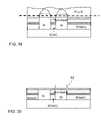
FIGS. 1-6 show structures according to a first embodiment of the invention;FIGS. 7-13 show structures according to a second embodiment of the invention;FIGS. 14-22 show structures according a third embodiment of the invention;FIG. 23 shows a schematic representation of a band alignment in accordance with an implementation of the invention;FIG. 24 shows a graph of out diffusion of Boron in a structure implementing aspects of the invention;FIG. 25 shows a final structure according to an aspect of the invention; andFIG. 26 shows a final structure according to an aspect of the invention.- This invention is directed to semiconductor structures and methods of manufacturing the semiconductor structures, and more particularly to structures and methods of forming SiGe and SiGeC buried layers for CMOS/BiCMOS and passive devices over Si or SOI substrates. In embodiments, the structures are formed on a silicon substrate which includes discontinuous buried layers having alternating regions of silicon and SiGe or SiGeC. In further embodiments, isolation trenches extend through the buried layer at the Si and SiGe or SiGeC interfaces to reduce defects between the alternating regions. This SiGe(C) film, for example, can be used to form the channel/well so the dopant diffusion can be suppressed.
- More specifically, multiple structures and methods are developed in accordance with the invention by burying SiGe and/or SiGeC films, doped and undoped, in conventional Si and SOI wafers to improve device characteristics, e.g., high voltage CMOS, PIN diode, high performance CMOS, circuit body effect, substrate current reduction and noise cross-talk, etc. The SiGe and/or SiGeC profiling has the capabilities to allow for bandgap modulation and formation of built in electric fields.
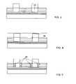
FIGS. 1-6 show structures according to a first embodiment of the invention. In this implementation, the SiGe or SiGeC film is formed above a BOX. As in each of the embodiments, the SiGe or SiGeC regions may be non-doped, or n-typed doped or p-typed doped, depending on the particular application.FIG. 1 shows a starting structure comprising anoptional BOX layer 12 formed on asilicon wafer 10. In embodiments, theBOX layer 12 is an oxide layer in a Si substrate. The oxide buried in the silicon wafer can be a depth ranging from less than 100 nm to several micrometers from the wafer surface, depending on the application. In embodiments, the thickness of theBOX layer 12 is in the range from about 40 nm to about 100 nm. A silicon (Si)film 14 is formed on theBOX layer 12.- In
FIG. 2 , anoptional buffer layer 16 is formed on theSi film 14. Theoptional buffer layer 16 may be a Si which is grown on the Sifilm 14. Theoptional buffer layer 16 forms a smooth, planar upper surface for further processing steps, thereby preventing any defects. As further shown inFIG. 2 , a SiGe or SiGeCfilm 18 is formed on thebuffer layer 16. In embodiments, the SiGe or SiGeCfilm 18 can be anywhere upwards of 4000 Å and in further embodiments can be about 5000 Å. The SiGe or SiGeC layer may be formed by conventional deposition methods such as, for example, low temperature epitaxy chemical vapor deposition (LTECVD). A Silicon (Si)epi layer 20 is formed on the SiGe or SiGeCfilm 18. The Ge and C composition can be in the range from any upwards to 40% and 5%, respectively. FIG. 3 represents a selective etching process to form troughs in the structure ofFIG. 2 . In this representative processing, a reactive ion etching (RIE) is undertaken to formtroughs 22 to theunderlying buffer layer 16. This RIE process is provided so that in the final structure only selective devices are formed on the SiGe or SiGeCfilm 18.- In
FIG. 4 , a secondSi epi layer 24 is formed over the entire structure. This process includes filling thetroughs 22 with theSi epi layer 24. - In
FIG. 5 , a chemical mechanical polishing (CMP) is performed to planarize the structure. Also, in a conventional manner,isolation structures 26 are formed between the interfaces of theSi epi layer 24 and SiGe orSiGeC film 18. The isolation structures may include, for example, shallow trench isolation structures (STI), deep trench isolation structures (DT) and/or trench isolation structures (TI), any of which will eliminate the defects which may exist between the interfaces of the Si layer and SiGe or SiGeC film. In embodiments, the STI structures may be about 4000 Å in depth, the TI structure may be about 2.5 microns and the DT structures may be about six microns in depth, any of which depend on the specific heights applications. FIGS. 6-13 show structures according to a second embodiment of the invention. In this implementation, the SiGe or SiGeC film is formed above the BOX.FIG. 6 shows a starting structure comprising anoptional BOX layer 12 formed on asilicon wafer 10. In embodiments, theBOX layer 12 is similar to that discussed with reference toFIG. 1 . Asilicon film 14 is formed on theBOX layer 12.- In
FIG. 7 , anSi epi layer 28 is formed on theSi film 14. TheSi epi layer 28 is formed to make a smooth upper surface for further processing steps, thereby preventing any defects in the final device. - As further shown, in
FIG. 8 a silicon dioxide orsilicon nitride layer 30 is formed over theSi epi layer 28. The silicon dioxide orsilicon nitride layer 30 is a hardmask, which is used for subsequent formation oftroughs 22, The trough depth is preferably to theSi film 14. By way of one illustrative example, a conventional photolithographic process is then performed to form thetrough etch openings 22, the hardmask is then removed from the opening as shown in the structure ofFIG. 8 . Then photoresist is stripped and troughs etch is conducted using remaining silicon dioxide or silicon nitride layer as the hardmask. The etch depth may be anywhere upwards of 4000 Å and in further embodiments can be about 5000 Å. - As shown in
FIG. 9 , an SiGe orSiGeC film 18 is grown in thetroughs 22. Asilicon film 32 is formed on the SiGe orSiGeC film 18 and the remaining structure. In embodiments, thesilicon film 32 may be formed by chemical vapor deposition (CVD) processes well known to those of skill in the art. As one of skill in the art should further understand, thesilicon film 32 will form apolysilicon 32aover the silicon dioxide orsilicon nitride 30 since there is no seed to nucleate to form single crystal. That is, the silicon will grow randomly forming thepolysilicon 32a. In contrast, thesilicon film 32 will remain in a single crystal form over the SiGe orSiGeC film 18. - As represented in
FIG. 10 , a chemical mechanical polishing (CMP) process is performed on the structure formed inFIG. 9 . The CMP will remove the damaged areas of thepolysilicon 32aandsilicon film 32. - In
FIG. 11 , an oxidation process is performed on the structure. In this manner, an oxide layer (dielectric layer)34 is formed over the structure. The oxidation process may be performed by any conventional oxidation growing process. - In
FIG. 12 , the oxide layer (dielectric layer)34 is wet stripped using any well known stripping process. For example, the oxide layer (dielectric layer)34 may be stripped using wet chemical processing. - In
FIG. 13 , after the wet strip process, in a conventional manner,isolation structures 26 are formed between the interfaces of theSilicon layer 28 and SiGe orSiGeC film 18. As discussed above, the isolation structures may include, for example, shallow trench isolation structures (STI), deep trench isolation structures (DT) and/or trench isolation structures (TI), any of which will be eliminate the defects which may exist between the interfaces of theSi layer 28 and SiGe orSiGeC film 18. In embodiments, the STI structures may be about 4000 Å, the TI structure may be about 2.5 microns and the DT structure may be about six microns, as discussed above. As further shown inFIG. 13 , anSi epi layer 38 may be formed over the structure. In embodiments, theSi epi layer 38 may be anywhere upwards of about 200 to 300 Å, and more preferably about 50 to 200 nm. FIGS. 14-22 show structures according a third embodiment of the invention. In this implementation, the SiGe or SiGeC film is formed below the BOX.FIG. 14 shows a starting structure comprising asilicon wafer 10.- In
FIG. 15 , a SiGe orSiGeC film 18 is formed on thesilicon wafer 10. In embodiments, the SiGe orSiGeC film 18 is grown on thesilicon wafer 10. Asilicon layer 40 is grown on the SiGe orSiGeC film 18. Thesilicon layer 40 may be about 500 Å; although thesilicon layer 40 may comprise different thicknesses as contemplated by the invention. - In
FIG. 16 , an oxide layer (dielectric layer)42 is formed via an oxygen ion implantation process. The oxidation process may be performed by any conventional oxidation implantation process. For example, a conventional SIMOX activation process is contemplated by the invention. In this manner, oxygen ions are implanted into the Si layer to form a buried oxide layer. The ion implantation energy is in a range of about 100 Kev to 250 kev. The oxygen dose is in a range of about 5E16 to 1E18 cm−2. The operating temperature is in a range of about 500 to 600° C. - As shown in
FIG. 17 , a silicon dioxide orsilicon nitride layer 44 is formed over theSi epi layer 40, which is worked as a hardmask. In a conventional manner, the hardmask is used for subsequent formation oftroughs 22, preferably to the underlying substrate. By way of one illustrative example, a conventional photolithographic process is then performed over the hardmask layer to form thetroughs 22. The dielectric is removed at the trough region to form the structure ofFIG. 17 . The etch depth may be anywhere upwards of 4000 Å and in further embodiments can be about 5000 Å. - In
FIG. 18 , anon-doped silicon film 50 is grown over the structure ofFIG. 17 , including within thetroughs 22. In embodiments, thesilicon film 50 may be formed by chemical vapor deposition (CVD) processes well known to those of skill in the art. As one of skill in the art should understand, thesilicon film 50 will form apolysilicon 50aover the silicon dioxide orsilicon nitride 44 since there is no seed to nucleate. That is, the silicon will grow randomly forming thepolysilicon 50a. In contrast, thesilicon film 50 will remain in a single crystal form over the SiGe orSiGeC film 18. - As represented in
FIG. 19 , a chemical mechanical polishing (CMP) process is performed on the structure. The CMP will remove the damaged areas of thepolysilicon 50aandsilicon film 50 down to the level oflayer 44. - In
FIG. 20 , a reoxidation process forms an oxide layer (dielectric layer)52 on the structure. The reoxidation process is a conventional process, well known to those of ordinary skill in the art such as discussed above. Theoxide layer 52 is wet cleaned using conventional processes such as, for example, a DHF process using dilute HF or buffered HF (BHF). In embodiments, the wet cleaning process removes contaminants from the wafer surface in the liquid-phase. As is known to those of skill in the art, wet cleaning chemistries are selected to form soluble compounds of surface contaminants; often enhanced by megasonic agitation and followed by deionized water rinse and dry cycle, for example. FIG. 21 shows a structure with smooth starting surface after wet clean process. InFIG. 22 , in a conventional manner, isolation structures26 (as discussed above) are formed between the interfaces of the Si and SiGe or SiGeC film. As discussed above, the isolation structures may include, for example, shallow trench isolation structures (STI), deep trench isolation structures (DT) and/or trench isolation structures (TI), any of which will be eliminate the defects which may exist between the interfaces of the Si layer and SiGe or SiGeC film.FIG. 23 shows a schematic representation of a band alignment in accordance with an implementation of the invention. As schematically shown, due to the fact of the band gap barrier, electrons, for example, in a FET, is more difficult to flow to the substrate due to the barrier provided by the SiGe (or SiGeC) doped areas of the structure. In this manner, the SiGe (or SiGeC) doped areas will direct the electrons into the source of the device which is normally grounded, blocking the electrons from flowing into the substrate. This will substantially decrease device leakage to the substrate or prevent the body current generated from other parts flow to this device.FIG. 24 shows a graph depicting out diffusion of Boron in a structure implementing aspects of the invention. In this graph, the diffusion of Boron is significantly decreased over SiGe (or SiGeC) doped areas of the structure. More specifically, out diffusion of Boron significantly decreases at SiGe (and SiGeC) doped areas. In this manner, in scaled devices implementing the structures of the invention, where the source and drain are very close together (e.g., 0.1 micron or less), the boron will not out diffuse and cause shorting of the device.- The method as described above is used in the fabrication of integrated circuit chips. The resulting integrated circuit chips can be distributed by the fabricator in raw wafer form (that is, as a single wafer that has multiple unpackaged chips), as a bare die, or in a packaged form. In the latter case the chip is mounted in a single chip package (such as a plastic carrier, with leads that are affixed to a motherboard or other higher level carrier) or in a multichip package (such as a ceramic carrier that has either or both surface interconnections or buried interconnections). In any case the chip is then integrated with other chips, discrete circuit elements, and/or other signal processing devices as part of either (a) an intermediate product, such as a motherboard, or (b) an end product. The end product can be any product that includes integrated circuit chips, ranging from toys and other low-end applications to advanced computer products having a display, a keyboard or other input device, and a central processor.
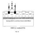
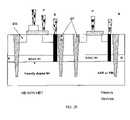
- By way of illustration, referring to
FIGS. 25 and 26 , final devices can be formed on the structures of the invention. For example, as shown inFIG. 25 , a CMOS device may be formed on the above BOX structures described with reference toFIGS. 1-13 . InFIG. 26 , an HB NPN HBT structure may be formed on the structures of the invention, as well as passive devices such as varactors and PIN diodes. - While the invention has been described in terms of exemplary embodiments, those skilled in the art will recognize that the invention can be practiced with modifications and in the spirit and scope of the appended claims.
Claims (20)
Priority Applications (3)
| Application Number | Priority Date | Filing Date | Title |
|---|---|---|---|
| US11/770,908US7989306B2 (en) | 2007-06-29 | 2007-06-29 | Method of forming alternating regions of Si and SiGe or SiGeC on a buried oxide layer on a substrate |
| US11/867,995US8138579B2 (en) | 2007-06-29 | 2007-10-05 | Structures and methods of forming SiGe and SiGeC buried layer for SOI/SiGe technology |
| US13/150,440US9087925B2 (en) | 2007-06-29 | 2011-06-01 | Si and SiGeC on a buried oxide layer on a substrate |
Applications Claiming Priority (1)
| Application Number | Priority Date | Filing Date | Title |
|---|---|---|---|
| US11/770,908US7989306B2 (en) | 2007-06-29 | 2007-06-29 | Method of forming alternating regions of Si and SiGe or SiGeC on a buried oxide layer on a substrate |
Related Child Applications (2)
| Application Number | Title | Priority Date | Filing Date |
|---|---|---|---|
| US11/867,995Continuation-In-PartUS8138579B2 (en) | 2007-06-29 | 2007-10-05 | Structures and methods of forming SiGe and SiGeC buried layer for SOI/SiGe technology |
| US13/150,440DivisionUS9087925B2 (en) | 2007-06-29 | 2011-06-01 | Si and SiGeC on a buried oxide layer on a substrate |
Publications (2)
| Publication Number | Publication Date |
|---|---|
| US20090001414A1true US20090001414A1 (en) | 2009-01-01 |
| US7989306B2 US7989306B2 (en) | 2011-08-02 |
Family
ID=40159313
Family Applications (2)
| Application Number | Title | Priority Date | Filing Date |
|---|---|---|---|
| US11/770,908Expired - Fee RelatedUS7989306B2 (en) | 2007-06-29 | 2007-06-29 | Method of forming alternating regions of Si and SiGe or SiGeC on a buried oxide layer on a substrate |
| US13/150,440Expired - Fee RelatedUS9087925B2 (en) | 2007-06-29 | 2011-06-01 | Si and SiGeC on a buried oxide layer on a substrate |
Family Applications After (1)
| Application Number | Title | Priority Date | Filing Date |
|---|---|---|---|
| US13/150,440Expired - Fee RelatedUS9087925B2 (en) | 2007-06-29 | 2011-06-01 | Si and SiGeC on a buried oxide layer on a substrate |
Country Status (1)
| Country | Link |
|---|---|
| US (2) | US7989306B2 (en) |
Families Citing this family (6)
| Publication number | Priority date | Publication date | Assignee | Title |
|---|---|---|---|---|
| US7696604B2 (en)* | 2007-10-23 | 2010-04-13 | International Business Machines Corporation | Silicon germanium heterostructure barrier varactor |
| US8575694B2 (en) | 2012-02-13 | 2013-11-05 | Taiwan Semiconductor Manufacturing Company, Ltd. | Insulated gate bipolar transistor structure having low substrate leakage |
| US9876110B2 (en) | 2014-01-31 | 2018-01-23 | Stmicroelectronics, Inc. | High dose implantation for ultrathin semiconductor-on-insulator substrates |
| US9337197B1 (en)* | 2014-10-28 | 2016-05-10 | Globalfoundries Inc. | Semiconductor structure having FinFET ultra thin body and methods of fabrication thereof |
| US9659960B1 (en) | 2015-12-09 | 2017-05-23 | International Business Machines Corporation | Extremely thin silicon-on-insulator silicon germanium device without edge strain relaxation |
| FR3098016A1 (en) | 2019-06-28 | 2021-01-01 | Stmicroelectronics (Crolles 2) Sas | Method of making a diode |
Citations (15)
| Publication number | Priority date | Publication date | Assignee | Title |
|---|---|---|---|---|
| US5882987A (en)* | 1997-08-26 | 1999-03-16 | International Business Machines Corporation | Smart-cut process for the production of thin semiconductor material films |
| US6288427B2 (en)* | 1999-08-31 | 2001-09-11 | International Business Machines Corporation | Silicon-germanium BiCMOS on SOI |
| US6365488B1 (en)* | 1998-03-05 | 2002-04-02 | Industrial Technology Research Institute | Method of manufacturing SOI wafer with buried layer |
| US6432754B1 (en)* | 2001-02-20 | 2002-08-13 | International Business Machines Corporation | Double SOI device with recess etch and epitaxy |
| US20020139977A1 (en)* | 2001-03-30 | 2002-10-03 | Samsung Electronics Co., Ltd. | SOI-type semiconductor device and method of forming the same |
| US20020168802A1 (en)* | 2001-05-14 | 2002-11-14 | Hsu Sheng Teng | SiGe/SOI CMOS and method of making the same |
| US6621131B2 (en)* | 2001-11-01 | 2003-09-16 | Intel Corporation | Semiconductor transistor having a stressed channel |
| US20030199126A1 (en)* | 2002-04-23 | 2003-10-23 | International Business Machines Corporation | Method of forming a SiGe-on-insulator substrate using separation by implantation of oxygen |
| US6765227B1 (en)* | 2001-02-26 | 2004-07-20 | Advanced Micro Devices, Inc. | Semiconductor-on-insulator (SOI) wafer having a Si/SiGe/Si active layer and method of fabrication using wafer bonding |
| US6833332B2 (en)* | 2002-01-04 | 2004-12-21 | International Business Machines Corporation | Method for fabrication of relaxed SiGe buffer layers on silicon-on-insulators and structures containing the same |
| US6914301B2 (en)* | 2000-01-07 | 2005-07-05 | Samsung Electronics Co., Ltd. | CMOS integrated circuit devices and substrates having buried silicon germanium layers therein and methods of forming same |
| US7265004B2 (en)* | 2005-11-14 | 2007-09-04 | Freescale Semiconductor, Inc. | Electronic devices including a semiconductor layer and a process for forming the same |
| US20080168418A1 (en)* | 2007-01-08 | 2008-07-10 | Freescale Semiconductor, Inc. | Integrated assist features for epitaxial growth bulk/SOI hybrid tiles with compensation |
| US20080274595A1 (en)* | 2007-05-01 | 2008-11-06 | Spencer Gregory S | Dual substrate orientation or bulk on SOI integrations using oxidation for silicon epitaxy spacer formation |
| US7554138B2 (en)* | 2004-06-16 | 2009-06-30 | Nxp B.V. | Method of manufacturing a strained semiconductor layer, method of manufacturing a semiconductor device and semiconductor substrate suitable for use in such a method including having a thin delta profile layer of germanium close to the bottom of the strained layer |
Family Cites Families (6)
| Publication number | Priority date | Publication date | Assignee | Title |
|---|---|---|---|---|
| KR100429869B1 (en) | 2000-01-07 | 2004-05-03 | 삼성전자주식회사 | CMOS Integrated circuit devices and substrates having buried silicon germanium layers therein and methods of forming same |
| KR100392166B1 (en)* | 2000-03-17 | 2003-07-22 | 가부시끼가이샤 도시바 | Semiconductor device and method for manufacturing the same |
| US6938237B1 (en) | 2001-06-29 | 2005-08-30 | Ellipsis Digital Systems, Inc. | Method, apparatus, and system for hardware design and synthesis |
| US20050116290A1 (en)* | 2003-12-02 | 2005-06-02 | De Souza Joel P. | Planar substrate with selected semiconductor crystal orientations formed by localized amorphization and recrystallization of stacked template layers |
| US7087965B2 (en)* | 2004-04-22 | 2006-08-08 | International Business Machines Corporation | Strained silicon CMOS on hybrid crystal orientations |
| US7253034B2 (en)* | 2004-07-29 | 2007-08-07 | International Business Machines Corporation | Dual SIMOX hybrid orientation technology (HOT) substrates |
- 2007
- 2007-06-29USUS11/770,908patent/US7989306B2/ennot_activeExpired - Fee Related
- 2011
- 2011-06-01USUS13/150,440patent/US9087925B2/ennot_activeExpired - Fee Related
Patent Citations (15)
| Publication number | Priority date | Publication date | Assignee | Title |
|---|---|---|---|---|
| US5882987A (en)* | 1997-08-26 | 1999-03-16 | International Business Machines Corporation | Smart-cut process for the production of thin semiconductor material films |
| US6365488B1 (en)* | 1998-03-05 | 2002-04-02 | Industrial Technology Research Institute | Method of manufacturing SOI wafer with buried layer |
| US6288427B2 (en)* | 1999-08-31 | 2001-09-11 | International Business Machines Corporation | Silicon-germanium BiCMOS on SOI |
| US6914301B2 (en)* | 2000-01-07 | 2005-07-05 | Samsung Electronics Co., Ltd. | CMOS integrated circuit devices and substrates having buried silicon germanium layers therein and methods of forming same |
| US6432754B1 (en)* | 2001-02-20 | 2002-08-13 | International Business Machines Corporation | Double SOI device with recess etch and epitaxy |
| US6765227B1 (en)* | 2001-02-26 | 2004-07-20 | Advanced Micro Devices, Inc. | Semiconductor-on-insulator (SOI) wafer having a Si/SiGe/Si active layer and method of fabrication using wafer bonding |
| US20020139977A1 (en)* | 2001-03-30 | 2002-10-03 | Samsung Electronics Co., Ltd. | SOI-type semiconductor device and method of forming the same |
| US20020168802A1 (en)* | 2001-05-14 | 2002-11-14 | Hsu Sheng Teng | SiGe/SOI CMOS and method of making the same |
| US6621131B2 (en)* | 2001-11-01 | 2003-09-16 | Intel Corporation | Semiconductor transistor having a stressed channel |
| US6833332B2 (en)* | 2002-01-04 | 2004-12-21 | International Business Machines Corporation | Method for fabrication of relaxed SiGe buffer layers on silicon-on-insulators and structures containing the same |
| US20030199126A1 (en)* | 2002-04-23 | 2003-10-23 | International Business Machines Corporation | Method of forming a SiGe-on-insulator substrate using separation by implantation of oxygen |
| US7554138B2 (en)* | 2004-06-16 | 2009-06-30 | Nxp B.V. | Method of manufacturing a strained semiconductor layer, method of manufacturing a semiconductor device and semiconductor substrate suitable for use in such a method including having a thin delta profile layer of germanium close to the bottom of the strained layer |
| US7265004B2 (en)* | 2005-11-14 | 2007-09-04 | Freescale Semiconductor, Inc. | Electronic devices including a semiconductor layer and a process for forming the same |
| US20080168418A1 (en)* | 2007-01-08 | 2008-07-10 | Freescale Semiconductor, Inc. | Integrated assist features for epitaxial growth bulk/SOI hybrid tiles with compensation |
| US20080274595A1 (en)* | 2007-05-01 | 2008-11-06 | Spencer Gregory S | Dual substrate orientation or bulk on SOI integrations using oxidation for silicon epitaxy spacer formation |
Also Published As
| Publication number | Publication date |
|---|---|
| US20110227130A1 (en) | 2011-09-22 |
| US7989306B2 (en) | 2011-08-02 |
| US9087925B2 (en) | 2015-07-21 |
Similar Documents
| Publication | Publication Date | Title |
|---|---|---|
| US9837321B2 (en) | Nonplanar device and strain-generating channel dielectric | |
| TWI655777B (en) | Switches with deep trench depletion and isolation structures | |
| US8003458B2 (en) | Methods of manufacturing a semiconductor device with active regions of different heights | |
| US7193254B2 (en) | Structure and method of applying stresses to PFET and NFET transistor channels for improved performance | |
| KR101065049B1 (en) | Modified Pinpet Channel Manufacturing Method | |
| US6764908B1 (en) | Narrow width CMOS devices fabricated on strained lattice semiconductor substrates with maximized NMOS and PMOS drive currents | |
| US9064799B2 (en) | Method of forming edge devices for improved performance | |
| US20180145150A1 (en) | High-k layer chamfering to prevent oxygen ingress in replacement metal gate (rmg) process | |
| US6936516B1 (en) | Replacement gate strained silicon finFET process | |
| CN101023530A (en) | High Mobility Bulk Silicon P-Channel Field Effect Transistor | |
| US20140048882A1 (en) | Techniques for gate workfunction engineering to reduce short channel effects in planar cmos devices | |
| US9087925B2 (en) | Si and SiGeC on a buried oxide layer on a substrate | |
| TWI699891B (en) | Laterally double diffused metal oxide semiconductor (ldmos) device on fully depleted silicon on insulator (fdsoi) enabling high input voltage | |
| CN103871893A (en) | BULK FIN FET WITH SUPER STEEP RETROGRADE WELL and manufacturing method of same | |
| US20120267724A1 (en) | Mos semiconductor device and methods for its fabrication | |
| US8138579B2 (en) | Structures and methods of forming SiGe and SiGeC buried layer for SOI/SiGe technology | |
| US8017472B2 (en) | CMOS devices having stress-altering material lining the isolation trenches and methods of manufacturing thereof | |
| KR101658706B1 (en) | A semiconduction structure having multiple semiconductor-device layers and methods for manufacturing the same | |
| US7528027B1 (en) | Structure and method for manufacturing device with ultra thin SOI at the tip of a V-shape channel | |
| US10680065B2 (en) | Field-effect transistors with a grown silicon-germanium channel | |
| US11843034B2 (en) | Lateral bipolar transistor | |
| US11705455B2 (en) | High voltage extended drain MOSFET (EDMOS) devices in a high-k metal gate (HKMG) | |
| US20080272401A1 (en) | Inverted Junction Field Effect Transistor and Method of Forming Thereof | |
| US20240395932A1 (en) | Wraparound gate structure | |
| US6872608B1 (en) | Method to selectively form poly SiGe P type electrode and polysilicon N type electrode through planarization |
Legal Events
| Date | Code | Title | Description |
|---|---|---|---|
| AS | Assignment | Owner name:INTERNATIONAL BUSINESS MACHINES CORPORATION, NEW Y Free format text:ASSIGNMENT OF ASSIGNORS INTEREST;ASSIGNORS:LIU, XUEFENG;RASSEL, ROBERT M;VOLDMAN, STEVEN H;REEL/FRAME:019498/0360;SIGNING DATES FROM 20070626 TO 20070628 Owner name:INTERNATIONAL BUSINESS MACHINES CORPORATION, NEW Y Free format text:ASSIGNMENT OF ASSIGNORS INTEREST;ASSIGNORS:LIU, XUEFENG;RASSEL, ROBERT M;VOLDMAN, STEVEN H;SIGNING DATES FROM 20070626 TO 20070628;REEL/FRAME:019498/0360 | |
| AS | Assignment | Owner name:INTERNATIONAL BUSINESS MACHINES CORPORATION, NEW Y Free format text:ASSIGNMENT OF ASSIGNORS INTEREST;ASSIGNORS:LIU, XUEFENG;RASSEL, ROBERT M.;VOLDMAN, STEVEN H.;REEL/FRAME:019994/0529;SIGNING DATES FROM 20071003 TO 20071004 Owner name:INTERNATIONAL BUSINESS MACHINES CORPORATION, NEW Y Free format text:ASSIGNMENT OF ASSIGNORS INTEREST;ASSIGNORS:LIU, XUEFENG;RASSEL, ROBERT M.;VOLDMAN, STEVEN H.;SIGNING DATES FROM 20071003 TO 20071004;REEL/FRAME:019994/0529 | |
| STCF | Information on status: patent grant | Free format text:PATENTED CASE | |
| REMI | Maintenance fee reminder mailed | ||
| FPAY | Fee payment | Year of fee payment:4 | |
| SULP | Surcharge for late payment | ||
| AS | Assignment | Owner name:GLOBALFOUNDRIES U.S. 2 LLC, NEW YORK Free format text:ASSIGNMENT OF ASSIGNORS INTEREST;ASSIGNOR:INTERNATIONAL BUSINESS MACHINES CORPORATION;REEL/FRAME:036550/0001 Effective date:20150629 | |
| AS | Assignment | Owner name:GLOBALFOUNDRIES INC., CAYMAN ISLANDS Free format text:ASSIGNMENT OF ASSIGNORS INTEREST;ASSIGNORS:GLOBALFOUNDRIES U.S. 2 LLC;GLOBALFOUNDRIES U.S. INC.;REEL/FRAME:036779/0001 Effective date:20150910 | |
| AS | Assignment | Owner name:WILMINGTON TRUST, NATIONAL ASSOCIATION, DELAWARE Free format text:SECURITY AGREEMENT;ASSIGNOR:GLOBALFOUNDRIES INC.;REEL/FRAME:049490/0001 Effective date:20181127 | |
| FEPP | Fee payment procedure | Free format text:MAINTENANCE FEE REMINDER MAILED (ORIGINAL EVENT CODE: REM.); ENTITY STATUS OF PATENT OWNER: LARGE ENTITY | |
| LAPS | Lapse for failure to pay maintenance fees | Free format text:PATENT EXPIRED FOR FAILURE TO PAY MAINTENANCE FEES (ORIGINAL EVENT CODE: EXP.); ENTITY STATUS OF PATENT OWNER: LARGE ENTITY | |
| STCH | Information on status: patent discontinuation | Free format text:PATENT EXPIRED DUE TO NONPAYMENT OF MAINTENANCE FEES UNDER 37 CFR 1.362 | |
| FP | Lapsed due to failure to pay maintenance fee | Effective date:20190802 | |
| AS | Assignment | Owner name:GLOBALFOUNDRIES INC., CAYMAN ISLANDS Free format text:RELEASE BY SECURED PARTY;ASSIGNOR:WILMINGTON TRUST, NATIONAL ASSOCIATION;REEL/FRAME:054636/0001 Effective date:20201117 | |
| AS | Assignment | Owner name:GLOBALFOUNDRIES U.S. INC., NEW YORK Free format text:RELEASE BY SECURED PARTY;ASSIGNOR:WILMINGTON TRUST, NATIONAL ASSOCIATION;REEL/FRAME:056987/0001 Effective date:20201117 |