US20090001344A1 - Memory cell that employs a selectively grown reversible resistance-switching element and methods of forming the same - Google Patents
Memory cell that employs a selectively grown reversible resistance-switching element and methods of forming the sameDownload PDFInfo
- Publication number
- US20090001344A1 US20090001344A1US11/772,088US77208807AUS2009001344A1US 20090001344 A1US20090001344 A1US 20090001344A1US 77208807 AUS77208807 AUS 77208807AUS 2009001344 A1US2009001344 A1US 2009001344A1
- Authority
- US
- United States
- Prior art keywords
- memory cell
- switching element
- reversible resistance
- tio
- diode
- Prior art date
- Legal status (The legal status is an assumption and is not a legal conclusion. Google has not performed a legal analysis and makes no representation as to the accuracy of the status listed.)
- Granted
Links
Images


Classifications
- H—ELECTRICITY
- H10—SEMICONDUCTOR DEVICES; ELECTRIC SOLID-STATE DEVICES NOT OTHERWISE PROVIDED FOR
- H10B—ELECTRONIC MEMORY DEVICES
- H10B63/00—Resistance change memory devices, e.g. resistive RAM [ReRAM] devices
- H10B63/80—Arrangements comprising multiple bistable or multi-stable switching components of the same type on a plane parallel to the substrate, e.g. cross-point arrays
- H10B63/84—Arrangements comprising multiple bistable or multi-stable switching components of the same type on a plane parallel to the substrate, e.g. cross-point arrays arranged in a direction perpendicular to the substrate, e.g. 3D cell arrays
- H—ELECTRICITY
- H10—SEMICONDUCTOR DEVICES; ELECTRIC SOLID-STATE DEVICES NOT OTHERWISE PROVIDED FOR
- H10B—ELECTRONIC MEMORY DEVICES
- H10B63/00—Resistance change memory devices, e.g. resistive RAM [ReRAM] devices
- H10B63/20—Resistance change memory devices, e.g. resistive RAM [ReRAM] devices comprising selection components having two electrodes, e.g. diodes
- H—ELECTRICITY
- H10—SEMICONDUCTOR DEVICES; ELECTRIC SOLID-STATE DEVICES NOT OTHERWISE PROVIDED FOR
- H10B—ELECTRONIC MEMORY DEVICES
- H10B63/00—Resistance change memory devices, e.g. resistive RAM [ReRAM] devices
- H10B63/30—Resistance change memory devices, e.g. resistive RAM [ReRAM] devices comprising selection components having three or more electrodes, e.g. transistors
- H—ELECTRICITY
- H10—SEMICONDUCTOR DEVICES; ELECTRIC SOLID-STATE DEVICES NOT OTHERWISE PROVIDED FOR
- H10B—ELECTRONIC MEMORY DEVICES
- H10B63/00—Resistance change memory devices, e.g. resistive RAM [ReRAM] devices
- H10B63/80—Arrangements comprising multiple bistable or multi-stable switching components of the same type on a plane parallel to the substrate, e.g. cross-point arrays
- H—ELECTRICITY
- H10—SEMICONDUCTOR DEVICES; ELECTRIC SOLID-STATE DEVICES NOT OTHERWISE PROVIDED FOR
- H10N—ELECTRIC SOLID-STATE DEVICES NOT OTHERWISE PROVIDED FOR
- H10N70/00—Solid-state devices having no potential barriers, and specially adapted for rectifying, amplifying, oscillating or switching
- H10N70/011—Manufacture or treatment of multistable switching devices
- H10N70/021—Formation of switching materials, e.g. deposition of layers
- H10N70/028—Formation of switching materials, e.g. deposition of layers by conversion of electrode material, e.g. oxidation
- H—ELECTRICITY
- H10—SEMICONDUCTOR DEVICES; ELECTRIC SOLID-STATE DEVICES NOT OTHERWISE PROVIDED FOR
- H10N—ELECTRIC SOLID-STATE DEVICES NOT OTHERWISE PROVIDED FOR
- H10N70/00—Solid-state devices having no potential barriers, and specially adapted for rectifying, amplifying, oscillating or switching
- H10N70/20—Multistable switching devices, e.g. memristors
- H—ELECTRICITY
- H10—SEMICONDUCTOR DEVICES; ELECTRIC SOLID-STATE DEVICES NOT OTHERWISE PROVIDED FOR
- H10N—ELECTRIC SOLID-STATE DEVICES NOT OTHERWISE PROVIDED FOR
- H10N70/00—Solid-state devices having no potential barriers, and specially adapted for rectifying, amplifying, oscillating or switching
- H10N70/801—Constructional details of multistable switching devices
- H10N70/821—Device geometry
- H10N70/826—Device geometry adapted for essentially vertical current flow, e.g. sandwich or pillar type devices
- H—ELECTRICITY
- H10—SEMICONDUCTOR DEVICES; ELECTRIC SOLID-STATE DEVICES NOT OTHERWISE PROVIDED FOR
- H10N—ELECTRIC SOLID-STATE DEVICES NOT OTHERWISE PROVIDED FOR
- H10N70/00—Solid-state devices having no potential barriers, and specially adapted for rectifying, amplifying, oscillating or switching
- H10N70/801—Constructional details of multistable switching devices
- H10N70/881—Switching materials
- H10N70/883—Oxides or nitrides
- H10N70/8833—Binary metal oxides, e.g. TaOx
Definitions
- the present inventionrelates to non-volatile memories and more particularly to a memory cell that employs a selectively grown reversible resistance-switching element and methods of forming the same.
- Non-volatile memories formed from reversible resistance-switching elementsare known.
- U.S. patent application Ser. No. 11/125,939filed May 9, 2005 and titled “REWRITEABLE MEMORY CELL COMPRISING A DIODE AND A RESISTANCE-SWITCHING MATERIAL” (hereinafter “the '939 application”), which is hereby incorporated by reference herein in its entirety for all purposes, describes a rewriteable non-volatile memory cell that includes a diode coupled in series with a reversible resistivity-switching material such as a metal oxide or metal nitride.
- a method of forming a memory cellincludes (1) forming a steering element above a substrate; and (2) forming a reversible resistance-switching element coupled to the steering element using a selective growth process.
- a method of forming a memory cellincludes (1) forming a first conductor above a substrate; (2) forming a titanium nitride layer above the first conductor; (3) selectively forming a reversible resistance-switching element by oxidizing the titanium nitride layer; (4) forming a vertical polycrystalline diode above the reversible resistance-switching element; and (5) forming a second conductor above the vertical polycrystalline diode.
- a method of forming a memory cellincludes (1) forming a thin film transistor having a source region and a drain region; (2) forming a first conductor coupled to the source region or the drain region of the transistor; (3) forming a titanium nitride layer above the first conductor; (4) selectively forming a reversible resistance-switching element by oxidizing the titanium nitride layer; and (5) forming a second conductor above the reversible resistance-switching element.
- a memory cellin a fifth aspect of the invention, includes (1) a steering element; and (2) a reversible resistance-switching element coupled to the steering element and formed using a selective growth process.
- a memory cellin a sixth aspect of the invention, includes (1) a first conductor; (2) a second conductor formed above the first conductor; (3) a diode formed between the first and second conductors; and (4) a reversible resistance-switching element formed between the first and second conductors using a selective growth process.
- a memory cellin a seventh aspect of the invention, includes (1) a first conductor; (2) a titanium nitride layer formed above the first conductor; (3) a reversible resistance-switching element selectively formed by oxidizing the titanium nitride layer; (4) a vertical polycrystalline diode formed above the reversible resistance-switching element; and (5) a second conductor formed above the vertical polycrystalline diode.
- a memory cellin an eighth aspect of the invention, includes (1) a thin film transistor having a source region and a drain region; (2) a first conductor coupled to the source region or the drain region; (3) a titanium nitride layer formed above the first conductor; (4) a reversible resistance-switching element selectively formed by oxidizing the titanium nitride layer; and (5) a second conductor formed above the reversible resistance-switching element.
- a plurality of non-volatile memory cellsinclude (1) a first plurality of substantially parallel, substantially coplanar conductors extending in a first direction; (2) a plurality of diodes; (3) a plurality of reversible resistance-switching elements; and (4) a second plurality of substantially parallel, substantially coplanar conductors extending in a second direction different from the first direction.
- one of the diodes and one of the reversible resistance-switching elementsare arranged in series, disposed between one of the first conductors and one of the second conductors.
- Each reversible resistance-switching elementis formed using a selective growth process.
- a monolithic three dimensional memory arrayin a tenth aspect of the invention, includes a first memory level formed above a substrate and having a plurality of memory cells. Each memory cell of the first memory level includes (1) a steering element; and (2) a reversible resistance-switching element coupled to the steering element and formed using a selective growth process.
- the monolithic three dimensional memory arrayalso includes at least a second memory level monolithically formed above the first memory level. Numerous other aspects are provided.
- FIG. 1is a schematic illustration of an exemplary memory cell provided in accordance with the present invention.
- FIG. 2Bis a simplified perspective view of a portion of a first memory level formed from a plurality of the memory cells of FIG. 2A .
- FIG. 2Cis a simplified perspective view of a portion of a first exemplary three dimensional memory array provided in accordance with the present invention.
- FIG. 2Dis a simplified perspective view of a portion of a second exemplary three dimensional memory array provided in accordance with the present invention.
- FIG. 5is a cross sectional view of an alternative memory cell provided in accordance with the present invention.
- fabricating memory devices from rewriteable resistivity-switching materialsis difficult.
- many rewriteable resistivity-switching materialsare difficult to etch chemically, increasing fabrication costs and complexity associated with their use in integrated circuits.
- a reversible resistance-switching elementmay be formed using titanium oxide as a reversible resistivity-switching material. Titanium oxide films have been shown to be suitable for use in memory cells, as described, for example, in the '939 application, previously incorporated.
- Titanium oxide filmssuch as TiO, TiO 2 , TiO x , TiO x N y , etc., are difficult to etch chemically.
- a titanium oxide layermay be used in a reversible resistance-switching element of a memory cell without the titanium oxide layer being etched.
- a reversible resistance-switching elementmay be formed by oxidizing a titanium-containing layer, such as titanium nitride, that is easier to pattern and etch than titanium oxide. In this manner, only the underlying titanium-containing layer (e.g., titanium nitride or titanium) is patterned and/or etched prior to oxidation of the titanium-containing layer and not the titanium oxide layer.
- titanium oxidemay be selectively formed by rapid thermal oxidation of a titanium-containing layer in an oxygen environment such as O 2 , ozone, a combination of the same, or using any other suitable oxidizing species.
- titanium oxidemay be formed by oxidizing a titanium-containing layer using oxygen diffusion in a chemical vapor deposition (CVD) chamber with an ozone or other oxygen source, using gaseous or liquid ozone cleaning, or using any other suitable oxidation process.
- CVDchemical vapor deposition
- reversible or one-time-programmable resistivity-switching materialsfor use in memory cells.
- a layer of Ta, TaN, Nb, NbN, Al, AlN, Hf, HfN, V, VN, etc.may be deposited on a substrate, patterned, etched and/or oxidized similarly to a titanium-containing layer so as to form a reversible resistivity-switching material such as Ta 2 O 5 , Nb 2 O 5 , Al 2 O 3 , HfO 2 , V 2 O 5 , etc.
- the reversible resistance-switching element 102includes a reversible resistivity-switching material (not separately shown) having a resistance that may be reversibly switched between two or more states.
- the reversible resistivity-switching material of the element 102may be in an initial, low-resistivity state upon fabrication that is switchable to a high-resistivity state upon application of a first voltage and/or current.
- Application of a second voltage and/or currentmay return the reversible resistivity-switching material to a low-resistivity state.
- the reversible resistance-switching element 102may be in an initial, high-resistance state upon fabrication that is reversibly switchable to a low-resistance state upon application of the appropriate voltage(s) and/or current(s).
- one resistance statemay represent a binary “0” while another resistance state may represent a binary “1”, although more than two data/resistance states may be used.
- Numerous reversible resistivity-switching materials and operation of memory cells employing reversible resistance-switching elementsare described, for example, in the '939 application, previously incorporated.
- the reversible resistance-switching element 102is formed using a selective growth process. As will be described further below, use of a selective growth process allows a reversible resistivity-switching material to be provided within the reversible resistance-switching element 102 without the reversible resistivity-switching material having to be etched. Fabrication of the reversible resistance-switching element 102 thereby is simplified.
- the steering element 104may include a thin film transistor, a diode, or another suitable steering element that exhibits non-ohmic conduction by selectively limiting the voltage across and/or the current flow through the reversible resistance-switching element 102 .
- the memory cell 100may be used as part of a two or three dimensional memory array and data may be written to and/or read from the memory cell 100 without affecting the state of other memory cells in the array.
- Exemplary embodiments of the memory cell 100 , the reversible resistance-switching element 102 and the steering element 104are described below with reference to FIGS. 2A-5 .
- FIG. 2Ais a simplified perspective view of a first embodiment of a memory cell 200 provided in accordance with the present invention.
- the memory cell 200includes a reversible resistance-switching element 202 (shown in phantom) coupled in series with a diode 204 between a first conductor 206 and a second conductor 208 .
- a barrier layer 209such as titanium nitride, tantalum nitride, tungsten nitride, etc., may be provided between the reversible resistance-switching element 202 and the diode 204 .
- the titanium oxide layer 212may include, for example, TiO, TiO 2 , TiO x , TiO x N y or the like. While the reversible resistance-switching element 202 is shown as being positioned below the diode 204 in FIG. 2A , it will be understood that in alternative embodiments, the reversible resistance-switching element 202 may be positioned above the diode 204 . Additional details for the reversible resistance-switching element 202 are described below with reference to FIG. 3 .
- the diode 204may include any suitable diode such as a vertical polycrystalline p-n or p-i-n diode, whether upward pointing with an n-region above a p-region of the diode or downward pointing with a p-region above an n-region of the diode. Exemplary embodiments of the diode 204 are described below with reference to FIG. 3 .
- the first and/or second conductor 206 , 208may include any suitable conductive material such as tungsten, any appropriate metal, heavily doped semiconductor material, a conductive silicide, a conductive silicide-germanide, a conductive germanide, or the like.
- the first and second conductors 206 , 208are rail-shaped and extend in different directions (e.g., substantially perpendicular to one another). Other conductor shapes and/or configurations may be used.
- barrier layers, adhesion layers, antireflection coatings and/or the likemay be used with the first and/or second conductors 206 , 208 to improve device performance and/or aid in device fabrication.
- reversible resistance-switching element 202may be used to form the reversible resistance-switching element 202 .
- materialssuch as Ta, TaN, Nb, NbN, Al, AlN, Hf, HfN, V, VN, etc., may be similarly deposited over (and/or patterned and etched with) the first conductor 206 and then oxidized to form the layer 212 , which includes the reversible resistance-switching element 202 .
- FIG. 2Bis a simplified perspective view of a portion of a first memory level 214 formed from a plurality of the memory cells 200 of FIG. 2A .
- the titanium-containing layer 210 and the titanium oxide layer 212are only shown on one of the bottom conductors 206 .
- the memory array 214is a “cross-point” array including a plurality of bit lines (second conductors 208 ) and word lines (first conductors 206 ) to which multiple memory cells are coupled (as shown).
- Other memory array configurationsmay be used, as may multiple levels of memory. For example, FIG.
- each memory level 218 , 220includes a plurality of memory cells 200 in a cross-point array.
- additional layerse.g., an interlevel dielectric
- FIG. 2COther memory array configurations may be used, as may additional levels of memory.
- all diodesmay “point” in the same direction, such as upward or downward depending on whether p-i-n diodes having a p-doped region on the bottom or top of the diode are employed, simplifying diode fabrication.
- the diodes of the first memory level 218may be upward pointing diodes as indicated by arrow A 1 (e.g., with p regions at the bottom of the diodes), while the diodes of the second memory level 220 may be downward pointing diodes as indicated by arrow A 2 (e.g., with n regions at the bottom of the diodes), or vice versa.
- a monolithic three dimensional memory arrayis one in which multiple memory levels are formed above a single substrate, such as a wafer, with no intervening substrates.
- the layers forming one memory levelare deposited or grown directly over the layers of an existing level or levels.
- stacked memorieshave been constructed by forming memory levels on separate substrates and adhering the memory levels atop each other, as in Leedy, U.S. Pat. No. 5,915,167, “Three dimensional structure memory.”
- the substratesmay be thinned or removed from the memory levels before bonding, but as the memory levels are initially formed over separate substrates, such memories are not true monolithic three dimensional memory arrays.
- FIG. 3is a cross-sectional view of an exemplary embodiment of the memory cell 200 of FIG. 2A .
- the memory cell 200includes the reversible resistance-switching element 202 (e.g., a portion of a layer of reversible resistivity-switching material, namely titanium oxide layer 212 in this embodiment), the diode 204 and the first and second conductors 206 , 208 .
- the reversible resistance-switching element 202may be a portion of the titanium oxide layer 212 that vertically overlies and/or overlaps with the diode 204 .
- the reversible resistance-switching element 202is formed by a selective growth process.
- the titanium oxide layer 212may be selectively formed on the titanium-containing layer 210 by oxidizing the titanium-containing layer 210 . In this manner, only the titanium-containing layer 210 , and not the titanium oxide layer 212 , is etched, such as during the pattern and etch step(s) for the first conductor 206 .
- the titanium-containing layer 210may be oxidized by any suitable process.
- the titanium-containing layer 210may be oxidized using thermal oxidation in oxygen, ozone, a combination of the same or another oxygen source (e.g., using rapid thermal oxidation).
- the titanium-containing layer 210may be oxidized using oxygen diffusion in a CVD chamber with an ozone or other oxygen source, using gaseous or liquid ozone cleaning, or using any other suitable oxidation process to form titanium oxide.
- other reversible resistance-switching materialsmay be similarly formed by oxidizing Ta, TaN, Nb, NbN, Al, AlN, Hf, HfN, V, VN, etc.
- rapid thermal oxidationmay be performed at a temperature of about 300° C. to about 800° C. for about one second to about 5 minutes at an oxygen flow rate of about 2 sccm to about 40 sccm, depending on the desired oxide thickness and/or other properties.
- oxygen flow rateof about 2 sccm to about 40 sccm, depending on the desired oxide thickness and/or other properties.
- Other oxidizing species, temperatures, times and/or flow ratesmay be used.
- Oxidation by ozone diffusion in a CVD chambermay be performed at a temperature of about 300° C. to about 800° C., more preferably at a temperature of about 350° C., to about 450° C., for about 2 minutes to about 4 hours, more preferably for about 15 to 25 minutes, at a suitable ozone flow rate, such as between about 10 and 60 sccm, depending on the desired oxide thickness and/or other properties.
- a suitable ozone flow ratesuch as between about 10 and 60 sccm, depending on the desired oxide thickness and/or other properties.
- Other oxidizing species, temperatures, times and/or flow ratesmay be used.
- titanium-containing layer 210is patterned and etched, and the need for etching of titanium oxide layers is eliminated. Memory cell fabrication is thereby significantly simplified. Further, any desired thickness of titanium oxide may be formed. In some embodiments, a titanium oxide layer thickness of about 500 angstroms or less, and more preferably about 300 angstroms or less, is employed for the reversible resistance-switching element 202 (although other thickness ranges may be used).
- the diode 204may be a vertical p-n or p-i-n diode, which may either point upward or downward.
- adjacent memory levelspreferably have diodes that point in opposite directions such as downward-pointing p-i-n diodes for a first memory level and upward-pointing p-i-n diodes for an adjacent, second memory level (or vice versa).
- the diode 204may be formed from a polycrystalline semiconductor material such as polysilicon, a polycrystalline silicon-germanium alloy, polygermanium or any other suitable material.
- the diode 204may include a heavily doped n+ polysilicon region 302 , a lightly doped or an intrinsic (unintentionally doped) polysilicon region 304 above the n+ polysilicon region 302 and a heavily doped, p+ polysilicon region 306 above the intrinsic region 304 .
- a thin (e.g., a few hundred angstroms or less) germanium and/or silicon-germanium alloy layer(not shown), with about 10 at % or more of germanium when using a silicon-germanium alloy layer, may be formed on the n+ polysilicon region 302 to prevent and/or reduce dopant migration from the n+ polysilicon region 302 into the intrinsic region 304 , as described, for example, in U.S. patent application Ser. No. 11/298,331, filed Dec.
- a barrier layer 308such as titanium nitride, tantalum nitride, tungsten nitride, etc., may be formed between the titanium oxide layer 212 and the n+ region 302 (e.g., to prevent and/or reduce migration of metal atoms into the polysilicon regions). Use of such a metal barrier layer may form an unwanted rectifying contact between the barrier layer 308 and the titanium oxide layer 212 . Accordingly, in some embodiments, a thin conductive layer (not shown), such as titanium, nickel, other conductive materials, etc., may be formed between the titanium oxide layer 212 and the barrier layer 308 (e.g., for work function tuning, to reduce or prevent formation of a rectifying contact).
- a silicide layer 310may be formed on the diode 204 to place the deposited silicon in a low resistivity state, as fabricated.
- a low resistivity stateallows for easier programming of the memory cell 200 as a large voltage is not required to switch the deposited silicon to a low resistivity state.
- a silicide-forming metal layer 312such as titanium or cobalt, may be deposited on the p+ polysilicon region 306 .
- the silicide-forming metal layer 312 and the deposited silicon of the diode 204interact to form the silicide layer 310 , consuming all or a portion of the silicide-forming metal layer 312 .
- silicide-forming materialssuch as titanium and cobalt react with deposited silicon during annealing to form a silicide layer.
- the lattice spacings of titanium silicide and cobalt silicideare close to that of silicon, and it appears that such silicide layers may serve as “crystallization templates” or “seeds” for adjacent deposited silicon as the deposited silicon crystallizes (e.g., the silicide layer 310 enhances the crystalline structure of the silicon diode 204 during annealing). Lower resistivity silicon thereby is provided. Similar results may be achieved for silicon-germanium alloy and/or germanium diodes.
- the top conductor 208is formed.
- one or more barrier layers and/or adhesion layers 314may be formed over the silicide-forming metal layer 312 prior to deposition of a conductive layer 315 .
- the conductive layer 315 , barrier layer 314 and silicide-forming metal layer 312may be patterned and/or etched together to form the top conductor 208 .
- the memory cell 200may be annealed to crystallize the deposited semiconductor material of the diode 204 (and/or to form the silicide layer 310 ).
- the annealmay be performed for about 10 seconds to about 2 minutes in nitrogen at a temperature of about 600 to 800° C., and more preferably between about 650 and 750° C. Other annealing times, temperatures and/or environments may be used.
- the silicide layer 310may serve as a “crystallization template” or “seed” during annealing for underlying deposited semiconductor material that forms the diode 204 . Lower resistivity diode material thereby is provided.
- FIGS. 4A-DAn exemplary process for fabricating a memory cell in accordance with the present invention is described below with reference to FIGS. 4A-D .
- FIGS. 4A-Dillustrate cross sectional views of a portion of a substrate 400 during fabrication of a first memory level in accordance with the present invention.
- the single memory levelincludes a plurality of memory cells that each include a reversible resistance-switching element formed using a selective growth process. Additional memory levels may be fabricated above the first memory level (as described previously with reference to FIGS. 2C-2D ).
- the substrate 400is shown as having already undergone several processing steps.
- the substrate 400may be any suitable substrate such as a silicon, germanium, silicon-germanium, undoped, doped, bulk, silicon-on-insulator (SOI) or other substrate with or without additional circuitry.
- the substrate 400may include one or more n-well or p-well regions (not shown).
- the isolation layer 402is formed above the substrate 400 .
- the isolation layer 402may be a layer of silicon dioxide, silicon nitride, silicon oxynitride or any other suitable insulating layer.
- the isolation layer 402may be a shallow trench isolation (STI) region formed by etching a trench in the substrate 400 , depositing a dielectric such as silicon dioxide, silicon nitride or another dielectric over the substrate 400 to fill the trench and planarizing the substrate 400 to re-expose a top surface 403 of the substrate 400 .
- STIshallow trench isolation
- a silicon nitride or similar protective layermay be formed over active regions (not shown) of the substrate 400 prior to isolation region formation (e.g., to protect the active regions).
- a localized oxidation of silicon (LOCOS) process or any other suitable processmay be employed to define the isolation layer 402 .
- an adhesion layer 404is formed over the isolation layer 402 (e.g., by physical vapor deposition or another method).
- the adhesion layer 404may be about 20 to about 500 angstroms, and preferably about 100 angstroms, of titanium nitride or another suitable adhesion layer such as tantalum nitride, tungsten nitride, combinations of one or more adhesion layers, or the like. Other adhesion layer materials and/or thicknesses may be employed.
- the adhesion layer 404may be optional.
- the conductive layer 406may include any suitable conductive material such as tungsten or another appropriate metal, heavily doped semiconductor material, a conductive silicide, a conductive silicide-germanide, a conductive germanide, or the like deposited by any suitable method (e.g., chemical vapor deposition, physical vapor deposition, etc.). In at least one embodiment, the conductive layer 406 may comprise about 200 to about 2500 angstroms of tungsten. Other conductive layer materials and/or thicknesses may be used.
- the adhesion layer 404 , the conductive layer 406 and the titanium-containing layer 407are patterned and etched.
- the adhesion layer 404 , the conductive layer 406 and the titanium-containing layer 407may be patterned and etched using conventional lithography techniques, with a soft or hard mask, and wet or dry etch processing.
- the adhesion layer 404 , the conductive layer 406 and the titanium-containing layer 407are patterned and etched so as to form substantially parallel, substantially co-planar conductors 408 (as shown in FIG. 4A ).
- Exemplary widths for the conductors 408 and/or spacings between the conductors 408range from about 200 to about 2500 angstroms, although other conductor widths and/or spacings may be used.
- a dielectric layer 410is deposited over the substrate 400 so as to fill the voids between the conductors 408 .
- a dielectric layer 410For example, approximately 3000-7000 angstroms of silicon dioxide may be deposited on the substrate 400 and planarized using chemical mechanical polishing or an etchback process to form a planar surface 412 .
- the planar surface 412includes exposed, discrete regions 407 a - f of titanium-containing layer material 407 separated by dielectric material 410 , as shown.
- the discrete titanium-containing layer regions 407 a - fmay be used to selectively form a titanium oxide reversible resistance-switching element for each memory cell being formed above the substrate 400 (as described further below).
- dielectric materialssuch as silicon nitride, silicon oxynitride, low K dielectrics, etc., and/or other dielectric layer thicknesses may be used.
- Exemplary low K dielectricsinclude carbon doped oxides, silicon carbon layers, or the like.
- the titanium-containing layer 407may be replaced with a layer of the material to be oxidized, such as Ta, TaN, Nb, NbN, Al, AlN, Hf, HfN, V, VN, etc.
- a reversible resistance-switching element 413 a - fis formed over each titanium-containing layer region 407 a - f .
- a titanium oxide layermay be selectively formed over each titanium-containing layer region 407 a - f by oxidizing the titanium-containing layer regions 407 a - f . Some or all of each titanium-containing layer region 407 a - f may be consumed during oxidation to create reversible resistance-switching elements 413 a - f .
- any suitable methodmay be employed to oxidize the titanium-containing layer regions 407 a - f such as rapid thermal oxidation in an oxygen environment such as O 2 , ozone, a combination of the same, or using any other suitable oxidizing species.
- a titanium-containing layer regionmay be oxidized using oxygen diffusion in a CVD chamber with an ozone or other oxygen source, using gaseous or liquid ozone cleaning, or using any other suitable oxidation process to form titanium oxide.
- the diode structures of each memory cellare formed.
- An optional thin conductive layer(not shown), such as about 10 to about 300 angstroms of titanium, nickel, etc., may be formed over the titanium oxide layer regions (e.g., for work function tuning).
- a barrier layer 414such as titanium nitride, tantalum nitride, tungsten nitride, etc., may also be formed over the titanium oxide layer regions prior to diode formation (e.g., to prevent and/or reduce migration of metal atoms into the polysilicon regions).
- the barrier layer 414may be on top of, in addition to or in place of the thin conductive layer and may be about 20 to about 500 angstroms, and preferably about 100 angstroms, of titanium nitride or another suitable barrier layer such as tantalum nitride, tungsten nitride, combinations of one or more barrier layers, barrier layers in combination with other layers such as titanium/titanium nitride, tantalum/tantalum nitride or tungsten/tungsten nitride stacks, or the like. Other barrier layer materials and/or thicknesses may be employed.
- each diodemay be a vertical p-n or p-i-n diode as previously described.
- each diodeis formed from a polycrystalline semiconductor material such as polysilicon, a polysilicon-germanium alloy, germanium or any other suitable material. For convenience, formation of a polysilicon, downward-pointing diode is described herein. It will be understood that other materials and/or diode configurations may be used.
- n+ silicon layer 416may be doped in situ, for example, by flowing a donor gas during deposition. Other doping methods may be used (e.g., implantation).
- a lightly doped, intrinsic and/or unintentionally doped silicon layer 418is formed over the n+ silicon layer 416 .
- the intrinsic silicon layer 418is in an amorphous state as deposited. In other embodiments, the intrinsic silicon layer 418 is in a polycrystalline state as deposited. Chemical vapor deposition or another suitable deposition method may be employed to deposit the intrinsic silicon layer 418 .
- the intrinsic silicon layer 418may be about 500 to about 4800 angstroms, preferably about 2500 angstroms, in thickness. Other intrinsic layer thicknesses may be used.
- a thin (e.g., a few hundred angstroms or less) germanium and/or silicon-germanium alloy layermay be formed on the n+ silicon layer 416 prior to deposition of the intrinsic silicon layer 418 to prevent and/or reduce dopant migration from the n+ silicon layer 416 into the intrinsic silicon layer 418 (as described in the '331 application, previously incorporated).
- the n+ silicon layer 416 and the intrinsic silicon layer 418are patterned and etched so as to form silicon pillars 420 overlying the conductors 408 (as shown).
- Conventional lithography techniques, with a soft or hard mask, and wet or dry etch processingmay be employed to form the silicon pillars 420 .
- a dielectric layer 422is deposited to fill the voids between the silicon pillars 420 .
- a dielectric layer 422is deposited to fill the voids between the silicon pillars 420 .
- silicon dioxidemay be deposited and planarized using chemical mechanical polishing or an etchback process to form a planar surface 424 .
- the planar surface 424includes exposed top surfaces of the silicon pillars 420 separated by dielectric material 422 , as shown.
- Other dielectric materialssuch as silicon nitride, silicon oxynitride, low K dielectrics, etc., and/or other dielectric layer thicknesses may be used.
- Exemplary low K dielectricsinclude carbon doped oxides, silicon carbon layers, or the like.
- the p+ silicon regions 426have a depth of about 100-700 angstroms, although other p+ silicon region sizes may be used. (Note that if the diodes to be formed are upward pointing p-n or p-i-n diodes, the upper portion of the silicon pillars 420 will be doped n-type). Each silicon pillar 420 thereby includes a downward-pointing, p-i-n diode 428 .
- a silicide-forming metal layer 430is deposited over the substrate 400 .
- exemplary silicide-forming metalsinclude sputter or otherwise deposited titanium or cobalt.
- the silicide-forming metal layer 430has a thickness of about 10 to about 200 angstroms, preferably about 20 to about 50 angstroms and more preferably about 20 angstroms. Other silicide-forming metal layer materials and/or thicknesses may be used.
- annealing of the structurecauses metal from the silicide-forming metal layer 430 and silicon from the p+ silicon regions 426 to react to form a silicide region 432 adjacent each p+ silicon region 426 .
- the conductive layer 440may be formed from any suitable conductive material such as tungsten, another suitable metal, heavily doped semiconductor material, a conductive silicide, a conductive silicide-germanide, a conductive germanide, or the like deposited by any suitable method (e.g., chemical vapor deposition, physical vapor deposition, etc.). Other conductive layer materials may be used.
- Barrier layers and/or adhesion layers 438may include titanium nitride or another suitable layer such as tantalum nitride, tungsten nitride, combinations of one or more layers, or any other suitable material(s).
- the structuremay be annealed to crystallize the deposited semiconductor material of the diodes 428 (and/or to form the silicide regions 432 ).
- the annealmay be performed for about 10 seconds to about 2 minutes in nitrogen at a temperature of about 600 to 800° C., and more preferably between about 650 and 750° C. Other annealing times, temperatures and/or environments may be used.
- the silicide regions 432may serve as “crystallization templates” or “seeds” during annealing for underlying deposited semiconductor material that forms the diodes 432 (e.g., changing any amorphous semiconductor material to polycrystalline semiconductor material and/or improving overall crystalline properties of the diodes 432 ). Lower resistivity diode material thereby is provided.
- FIG. 5is a cross sectional view of an exemplary memory cell 500 provided in accordance with the present invention.
- the memory cell 500includes a thin film transistor (TFT), such as a thin film, metal oxide semiconductor field effect transistor (MOSFET) 502 coupled to a reversible resistance-switching element 504 formed above a substrate 505 .
- TFTthin film transistor
- MOSFETmetal oxide semiconductor field effect transistor
- the MOSFET 502may be an n-channel or a p-channel thin film MOSFET formed on any suitable substrate.
- an insulating region 506such as silicon dioxide, silicon nitride, oxynitride, etc.
- a deposited semiconductor region 507such as deposited silicon, germanium, silicon-germanium, etc.
- the thin film MOSFET 502is formed within the deposited semiconductor region 507 and is insulated from the substrate 505 by the insulating region 506 .
- the MOSFET 502includes source/drain regions 508 , 510 and channel region 512 , as well as gate dielectric layer 514 , gate electrode 516 and spacers 518 a - b .
- the source/drain regions 508 , 510may be doped p-type and the channel region 512 may be doped n-type, while in other embodiments the source/drain regions 508 , 510 may be doped n-type and the channel region 512 may be doped p-type. Any other MOSFET configuration or any suitable fabrication techniques may be employed for the thin film MOSFET 502 .
- the MOSFET 502may be electrically isolated by isolation regions (not shown) formed in the substrate 506 (e.g., formed using an STI, LOCOS or other similar process). Alternatively, gate, source and/or drain regions of the MOSFET 502 may be shared with other transistors (not shown) formed on the substrate 506 .
- the reversible resistance-switching element 504includes a lower conductor 520 , a titanium-containing layer 521 formed over the lower conductor 520 , a titanium oxide layer 522 selectively grown over the titanium-containing layer 521 and an upper conductor 524 formed over the reversible resistivity-switching material (titanium oxide layer 522 ).
- the upper and lower conductors 520 , 524may include any suitable conductive material such as tungsten, another metal, heavily doped semiconductor material, a conductive silicide, a conductive silicide-germanide, a conductive germanide, or the like.
- one or more barrier and/or adhesion layersmay be provided between the upper and lower conductors 520 , 524 and the reversible resistivity-switching material (titanium oxide layer 522 ).
- the reversible resistivity-switching material(titanium oxide layer 522 ) is formed using a selective growth process as previously described with reference to the embodiments of FIGS. 1-4D .
- the titanium oxide layer 522may be selectively formed by rapid thermal oxidation of the titanium-containing layer 521 in an oxygen environment such as O 2 , ozone, a combination of the same, or using any other suitable oxidizing species.
- the titanium oxide layer 522may be formed by oxidizing the titanium-containing layer 521 using oxygen diffusion in a chemical vapor deposition (CVD) chamber with an ozone or other oxygen source, using gaseous or liquid ozone cleaning, or using any other suitable oxidation process.
- CVDchemical vapor deposition
- etching of titanium oxide layersmay be eliminated and memory cell fabrication significantly simplified.
- Other materialsmay be selectively oxidized in accordance with the present invention to form reversible resistivity-switching materials for use in memory cell 500 (e.g., Ta, TaN, Nb, NbN, Al, AlN, Hf, HfN, V, VN, etc.).
- the reversible resistance-switching element 504is coupled to the source/drain region 510 of the MOSFET 502 by a first conductive plug 526 and to a first metal level (M 1 ) line 528 by a second conductive plug 530 (which extend through a dielectric layer 532 ).
- a third conductive plug 534couples the source/drain region 508 of the MOSFET 502 to an M 1 line 536 .
- the conductive plugs and/or linesmay be formed from any suitable materials (without or without barriers layers) such as tungsten, another metal, heavily doped semiconductor material, a conductive silicide, a conductive silicide-germanide, a conductive germanide, or the like.
- the dielectric layer 532may include any suitable dielectric such as silicon dioxide, silicon nitride, silicon oxynitride, low K dielectrics, etc.
- the thin film MOSFET 502operates as a steering element in a manner similar to that of the diodes employed in the memory cells of FIGS. 2A-4D , selectively limiting the voltage applied across and/or the current flow through the reversible resistance-switching element 504 .
- the reversible resistance-switching element 504includes a titanium oxide layer having a thickness of about 500 angstroms or less, and more preferably a thickness of about 300 angstroms or less. Other titanium oxide thicknesses may be employed.
Landscapes
- Semiconductor Memories (AREA)
Abstract
Description
- The present application is related to the following patent applications, each of which is hereby incorporated by reference herein in its entirety for all purposes:
- U.S. patent application Ser. No. ______, filed on even date herewith and titled “METHOD TO FORM A REWRITEABLE MEMORY CELL COMPRISING A DIODE AND A RESISTIVITY-SWITCHING GROWN OXIDE” (Docket No. MD-304X).
- U.S. patent application Ser. No. ______, filed on even date herewith and titled “MEMORY CELL THAT EMPLOYS A SELECTIVELY DEPOSITED REVERSIBLE RESISTANCE-SWITCHING ELEMENT AND METHODS OF FORMING THE SAME” (Docket No. MD-333X).
- U.S. patent application Ser. No. ______, filed on even date herewith and titled “MEMORY CELL THAT EMPLOYS A SELECTIVELY DEPOSITED REVERSIBLE RESISTANCE-SWITCHING ELEMENT AND METHODS OF FORMING THE SAME” (Docket No. MD-333Y).
- The present invention relates to non-volatile memories and more particularly to a memory cell that employs a selectively grown reversible resistance-switching element and methods of forming the same.
- Non-volatile memories formed from reversible resistance-switching elements are known. For example, U.S. patent application Ser. No. 11/125,939, filed May 9, 2005 and titled “REWRITEABLE MEMORY CELL COMPRISING A DIODE AND A RESISTANCE-SWITCHING MATERIAL” (hereinafter “the '939 application”), which is hereby incorporated by reference herein in its entirety for all purposes, describes a rewriteable non-volatile memory cell that includes a diode coupled in series with a reversible resistivity-switching material such as a metal oxide or metal nitride.
- However, fabricating memory devices from rewriteable resistivity-switching materials is difficult; and improved methods of forming memory devices that employ reversible resistivity-switching materials are desirable.
- In a first aspect of the invention, a method of forming a memory cell is provided that includes (1) forming a steering element above a substrate; and (2) forming a reversible resistance-switching element coupled to the steering element using a selective growth process.
- In a second aspect of the invention, a method of forming a memory cell is provided that includes (1) forming a first conductor above a substrate; (2) forming a reversible resistance-switching element above the first conductor using a selective growth process; (3) forming a diode above the first conductor; and (4) forming a second conductor above the diode and the reversible resistance-switching element.
- In a third aspect of the invention, a method of forming a memory cell is provided that includes (1) forming a first conductor above a substrate; (2) forming a titanium nitride layer above the first conductor; (3) selectively forming a reversible resistance-switching element by oxidizing the titanium nitride layer; (4) forming a vertical polycrystalline diode above the reversible resistance-switching element; and (5) forming a second conductor above the vertical polycrystalline diode.
- In a fourth aspect of the invention, a method of forming a memory cell is provided that includes (1) forming a thin film transistor having a source region and a drain region; (2) forming a first conductor coupled to the source region or the drain region of the transistor; (3) forming a titanium nitride layer above the first conductor; (4) selectively forming a reversible resistance-switching element by oxidizing the titanium nitride layer; and (5) forming a second conductor above the reversible resistance-switching element.
- In a fifth aspect of the invention, a memory cell is provided that includes (1) a steering element; and (2) a reversible resistance-switching element coupled to the steering element and formed using a selective growth process.
- In a sixth aspect of the invention, a memory cell is provided that includes (1) a first conductor; (2) a second conductor formed above the first conductor; (3) a diode formed between the first and second conductors; and (4) a reversible resistance-switching element formed between the first and second conductors using a selective growth process.
- In a seventh aspect of the invention, a memory cell is provided that includes (1) a first conductor; (2) a titanium nitride layer formed above the first conductor; (3) a reversible resistance-switching element selectively formed by oxidizing the titanium nitride layer; (4) a vertical polycrystalline diode formed above the reversible resistance-switching element; and (5) a second conductor formed above the vertical polycrystalline diode.
- In an eighth aspect of the invention, a memory cell is provided that includes (1) a thin film transistor having a source region and a drain region; (2) a first conductor coupled to the source region or the drain region; (3) a titanium nitride layer formed above the first conductor; (4) a reversible resistance-switching element selectively formed by oxidizing the titanium nitride layer; and (5) a second conductor formed above the reversible resistance-switching element.
- In a ninth aspect of the invention, a plurality of non-volatile memory cells are provided that include (1) a first plurality of substantially parallel, substantially coplanar conductors extending in a first direction; (2) a plurality of diodes; (3) a plurality of reversible resistance-switching elements; and (4) a second plurality of substantially parallel, substantially coplanar conductors extending in a second direction different from the first direction. In each memory cell, one of the diodes and one of the reversible resistance-switching elements are arranged in series, disposed between one of the first conductors and one of the second conductors. Each reversible resistance-switching element is formed using a selective growth process.
- In a tenth aspect of the invention, a monolithic three dimensional memory array is provided that includes a first memory level formed above a substrate and having a plurality of memory cells. Each memory cell of the first memory level includes (1) a steering element; and (2) a reversible resistance-switching element coupled to the steering element and formed using a selective growth process. The monolithic three dimensional memory array also includes at least a second memory level monolithically formed above the first memory level. Numerous other aspects are provided.
- Other features and aspects of the present invention will become more fully apparent from the following detailed description, the appended claims and the accompanying drawings.
FIG. 1 is a schematic illustration of an exemplary memory cell provided in accordance with the present invention.FIG. 2A is a simplified perspective view of a first embodiment of a memory cell provided in accordance with the present invention.FIG. 2B is a simplified perspective view of a portion of a first memory level formed from a plurality of the memory cells ofFIG. 2A .FIG. 2C is a simplified perspective view of a portion of a first exemplary three dimensional memory array provided in accordance with the present invention.FIG. 2D is a simplified perspective view of a portion of a second exemplary three dimensional memory array provided in accordance with the present invention.FIG. 3 is a cross-sectional view of an exemplary embodiment of the memory cell ofFIG. 2A .FIGS. 4A-D illustrate cross sectional views of a portion of a substrate during fabrication of a single memory level in accordance with the present invention.FIG. 5 is a cross sectional view of an alternative memory cell provided in accordance with the present invention.- As stated above, fabricating memory devices from rewriteable resistivity-switching materials is difficult. For example, many rewriteable resistivity-switching materials are difficult to etch chemically, increasing fabrication costs and complexity associated with their use in integrated circuits.
- In accordance with the present invention, difficult-to-etch-chemically rewriteable resistivity-switching materials may be used within a memory cell without being etched. For example, in at least one embodiment, a memory cell is provided that includes a reversible resistivity-switching material formed using a selective growth process so that the reversible resistivity-switching material may be used within the memory cell without being etched.
- In one or more exemplary embodiments, a reversible resistance-switching element may be formed using titanium oxide as a reversible resistivity-switching material. Titanium oxide films have been shown to be suitable for use in memory cells, as described, for example, in the '939 application, previously incorporated.
- Titanium oxide films such as TiO, TiO2, TiOx, TiOxNy, etc., are difficult to etch chemically. In at least one embodiment, through use of a selective growth process, a titanium oxide layer may be used in a reversible resistance-switching element of a memory cell without the titanium oxide layer being etched. For example, a reversible resistance-switching element may be formed by oxidizing a titanium-containing layer, such as titanium nitride, that is easier to pattern and etch than titanium oxide. In this manner, only the underlying titanium-containing layer (e.g., titanium nitride or titanium) is patterned and/or etched prior to oxidation of the titanium-containing layer and not the titanium oxide layer.
- In some embodiments, titanium oxide may be selectively formed by rapid thermal oxidation of a titanium-containing layer in an oxygen environment such as O2, ozone, a combination of the same, or using any other suitable oxidizing species. In other embodiments, titanium oxide may be formed by oxidizing a titanium-containing layer using oxygen diffusion in a chemical vapor deposition (CVD) chamber with an ozone or other oxygen source, using gaseous or liquid ozone cleaning, or using any other suitable oxidation process. In any case, the need for etching of titanium oxide layers may be eliminated and memory cell fabrication significantly simplified.
- Other materials may be selectively oxidized in accordance with the present invention to form reversible or one-time-programmable resistivity-switching materials for use in memory cells. For example, a layer of Ta, TaN, Nb, NbN, Al, AlN, Hf, HfN, V, VN, etc., may be deposited on a substrate, patterned, etched and/or oxidized similarly to a titanium-containing layer so as to form a reversible resistivity-switching material such as Ta2O5, Nb2O5, Al2O3, HfO2, V2O5, etc.
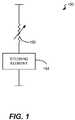
FIG. 1 is a schematic illustration of anexemplary memory cell 100 provided in accordance with the present invention. Thememory cell 100 includes a reversible resistance-switchingelement 102 coupled to asteering element 104.- The reversible resistance-switching
element 102 includes a reversible resistivity-switching material (not separately shown) having a resistance that may be reversibly switched between two or more states. For example, the reversible resistivity-switching material of theelement 102 may be in an initial, low-resistivity state upon fabrication that is switchable to a high-resistivity state upon application of a first voltage and/or current. Application of a second voltage and/or current may return the reversible resistivity-switching material to a low-resistivity state. Alternatively, the reversible resistance-switchingelement 102 may be in an initial, high-resistance state upon fabrication that is reversibly switchable to a low-resistance state upon application of the appropriate voltage(s) and/or current(s). When used in a memory cell, one resistance state may represent a binary “0” while another resistance state may represent a binary “1”, although more than two data/resistance states may be used. Numerous reversible resistivity-switching materials and operation of memory cells employing reversible resistance-switching elements are described, for example, in the '939 application, previously incorporated. - In at least one embodiment of the invention, the reversible resistance-switching
element 102 is formed using a selective growth process. As will be described further below, use of a selective growth process allows a reversible resistivity-switching material to be provided within the reversible resistance-switchingelement 102 without the reversible resistivity-switching material having to be etched. Fabrication of the reversible resistance-switchingelement 102 thereby is simplified. - The
steering element 104 may include a thin film transistor, a diode, or another suitable steering element that exhibits non-ohmic conduction by selectively limiting the voltage across and/or the current flow through the reversible resistance-switchingelement 102. In this manner, thememory cell 100 may be used as part of a two or three dimensional memory array and data may be written to and/or read from thememory cell 100 without affecting the state of other memory cells in the array. - Exemplary embodiments of the
memory cell 100, the reversible resistance-switchingelement 102 and thesteering element 104 are described below with reference toFIGS. 2A-5 . FIG. 2A is a simplified perspective view of a first embodiment of amemory cell 200 provided in accordance with the present invention. With reference toFIG. 2A , thememory cell 200 includes a reversible resistance-switching element202 (shown in phantom) coupled in series with adiode 204 between afirst conductor 206 and asecond conductor 208. In some embodiments, abarrier layer 209 such as titanium nitride, tantalum nitride, tungsten nitride, etc., may be provided between the reversible resistance-switchingelement 202 and thediode 204.- As will be described further below, the reversible resistance-switching
element 202 is selectively formed so as to simplify fabrication of thememory cell 200. In at least one embodiment, the reversible resistance-switchingelement 202 includes at least a portion of a titanium oxide layer formed by oxidizing a titanium-containing layer such as titanium nitride. For example, a titanium nitride layer or another similar form of titanium may be deposited above or below thediode 204, patterned and etched (e.g., such as with the first conductor206). The titanium nitride (or other) layer then may be oxidized to form titanium oxide (e.g., using rapid thermal oxidation or another oxidation process). - In the embodiment of
FIG. 2A , a titanium nitride orsimilar layer 210 is formed over, and is patterned and etched with, thefirst conductor 206. The titanium nitride orsimilar layer 210 then is oxidized to form atitanium oxide layer 212. A portion of thetitanium oxide layer 212 that vertically overlaps and/or aligns with thediode 204 may serve as the reversible resistance-switchingelement 202 between thediode 204 and thefirst conductor 206 of thememory cell 200. In some embodiments, only a portion, such as one or more filaments, of the reversible resistance-switchingelement 202 may switch and/or be switchable. Thetitanium oxide layer 212 may include, for example, TiO, TiO2, TiOx, TiOxNyor the like. While the reversible resistance-switchingelement 202 is shown as being positioned below thediode 204 inFIG. 2A , it will be understood that in alternative embodiments, the reversible resistance-switchingelement 202 may be positioned above thediode 204. Additional details for the reversible resistance-switchingelement 202 are described below with reference toFIG. 3 . - The
diode 204 may include any suitable diode such as a vertical polycrystalline p-n or p-i-n diode, whether upward pointing with an n-region above a p-region of the diode or downward pointing with a p-region above an n-region of the diode. Exemplary embodiments of thediode 204 are described below with reference toFIG. 3 . - The first and/or
second conductor FIG. 2A , the first andsecond conductors second conductors - As stated, other materials may be used to form the reversible resistance-switching
element 202. For example, materials such as Ta, TaN, Nb, NbN, Al, AlN, Hf, HfN, V, VN, etc., may be similarly deposited over (and/or patterned and etched with) thefirst conductor 206 and then oxidized to form thelayer 212, which includes the reversible resistance-switchingelement 202. FIG. 2B is a simplified perspective view of a portion of afirst memory level 214 formed from a plurality of thememory cells 200 ofFIG. 2A . For simplicity, the titanium-containinglayer 210 and thetitanium oxide layer 212 are only shown on one of thebottom conductors 206. Thememory array 214 is a “cross-point” array including a plurality of bit lines (second conductors208) and word lines (first conductors206) to which multiple memory cells are coupled (as shown). Other memory array configurations may be used, as may multiple levels of memory. For example,FIG. 2C is a simplified perspective view of a portion of a monolithic threedimensional array 216 that includes afirst memory level 218 positioned below asecond memory level 220. In the embodiment ofFIG. 2C , eachmemory level memory cells 200 in a cross-point array. It will be understood that one or more additional layers (e.g., an interlevel dielectric) may be present between the first andsecond memory levels FIG. 2C for simplicity. Other memory array configurations may be used, as may additional levels of memory. In the embodiment ofFIG. 2C , all diodes may “point” in the same direction, such as upward or downward depending on whether p-i-n diodes having a p-doped region on the bottom or top of the diode are employed, simplifying diode fabrication.- In some embodiments, the memory levels may be formed, as described, for example, in U.S. Pat. No. 6,952,030, “High-density three-dimensional memory cell” which is hereby incorporated by reference herein in its entirety for all purposes. For instance, the upper conductors of a first memory level may be used as the lower conductors of a second memory level that is positioned above the first memory level as shown in
FIG. 2D . In such embodiments, the diodes on adjacent memory levels preferably point in opposite directions as described in U.S. patent application Ser. No. 11/692,151, filed Mar. 27, 2007 and titled “LARGE ARRAY OF UPWARD POINTING P-I-N DIODES HAVING LARGE AND UNIFORM CURRENT” (hereinafter “the '151 application”), which is hereby incorporated by reference herein in its entirety for all purposes. For example, the diodes of thefirst memory level 218 may be upward pointing diodes as indicated by arrow A1(e.g., with p regions at the bottom of the diodes), while the diodes of thesecond memory level 220 may be downward pointing diodes as indicated by arrow A2(e.g., with n regions at the bottom of the diodes), or vice versa. - A monolithic three dimensional memory array is one in which multiple memory levels are formed above a single substrate, such as a wafer, with no intervening substrates. The layers forming one memory level are deposited or grown directly over the layers of an existing level or levels. In contrast, stacked memories have been constructed by forming memory levels on separate substrates and adhering the memory levels atop each other, as in Leedy, U.S. Pat. No. 5,915,167, “Three dimensional structure memory.” The substrates may be thinned or removed from the memory levels before bonding, but as the memory levels are initially formed over separate substrates, such memories are not true monolithic three dimensional memory arrays.
FIG. 3 is a cross-sectional view of an exemplary embodiment of thememory cell 200 ofFIG. 2A . With reference toFIG. 3 , thememory cell 200 includes the reversible resistance-switching element202 (e.g., a portion of a layer of reversible resistivity-switching material, namelytitanium oxide layer 212 in this embodiment), thediode 204 and the first andsecond conductors element 202 may be a portion of thetitanium oxide layer 212 that vertically overlies and/or overlaps with thediode 204.- In the embodiment of
FIG. 3 , the reversible resistance-switchingelement 202 is formed by a selective growth process. For example, thetitanium oxide layer 212 may be selectively formed on the titanium-containinglayer 210 by oxidizing the titanium-containinglayer 210. In this manner, only the titanium-containinglayer 210, and not thetitanium oxide layer 212, is etched, such as during the pattern and etch step(s) for thefirst conductor 206. - The titanium-containing
layer 210 may be oxidized by any suitable process. For instance, the titanium-containinglayer 210 may be oxidized using thermal oxidation in oxygen, ozone, a combination of the same or another oxygen source (e.g., using rapid thermal oxidation). Alternatively or additionally, the titanium-containinglayer 210 may be oxidized using oxygen diffusion in a CVD chamber with an ozone or other oxygen source, using gaseous or liquid ozone cleaning, or using any other suitable oxidation process to form titanium oxide. As stated, other reversible resistance-switching materials may be similarly formed by oxidizing Ta, TaN, Nb, NbN, Al, AlN, Hf, HfN, V, VN, etc. - In one exemplary embodiment, rapid thermal oxidation may be performed at a temperature of about 300° C. to about 800° C. for about one second to about 5 minutes at an oxygen flow rate of about 2 sccm to about 40 sccm, depending on the desired oxide thickness and/or other properties. Other oxidizing species, temperatures, times and/or flow rates may be used.
- Oxidation by ozone diffusion in a CVD chamber may be performed at a temperature of about 300° C. to about 800° C., more preferably at a temperature of about 350° C., to about 450° C., for about 2 minutes to about 4 hours, more preferably for about 15 to 25 minutes, at a suitable ozone flow rate, such as between about 10 and 60 sccm, depending on the desired oxide thickness and/or other properties. Other oxidizing species, temperatures, times and/or flow rates may be used.
- In each of the above cases, only the titanium-containing
layer 210 is patterned and etched, and the need for etching of titanium oxide layers is eliminated. Memory cell fabrication is thereby significantly simplified. Further, any desired thickness of titanium oxide may be formed. In some embodiments, a titanium oxide layer thickness of about 500 angstroms or less, and more preferably about 300 angstroms or less, is employed for the reversible resistance-switching element202 (although other thickness ranges may be used). - As stated, the
diode 204 may be a vertical p-n or p-i-n diode, which may either point upward or downward. In the embodiment ofFIG. 2D in which adjacent memory levels share conductors, adjacent memory levels preferably have diodes that point in opposite directions such as downward-pointing p-i-n diodes for a first memory level and upward-pointing p-i-n diodes for an adjacent, second memory level (or vice versa). - In some embodiments, the
diode 204 may be formed from a polycrystalline semiconductor material such as polysilicon, a polycrystalline silicon-germanium alloy, polygermanium or any other suitable material. For example, thediode 204 may include a heavily dopedn+ polysilicon region 302, a lightly doped or an intrinsic (unintentionally doped)polysilicon region 304 above then+ polysilicon region 302 and a heavily doped,p+ polysilicon region 306 above theintrinsic region 304. In some embodiments, a thin (e.g., a few hundred angstroms or less) germanium and/or silicon-germanium alloy layer (not shown), with about 10 at % or more of germanium when using a silicon-germanium alloy layer, may be formed on then+ polysilicon region 302 to prevent and/or reduce dopant migration from then+ polysilicon region 302 into theintrinsic region 304, as described, for example, in U.S. patent application Ser. No. 11/298,331, filed Dec. 9, 2005 and titled “DEPOSITED SEMICONDUCTOR STRUCTURE TO MINIMIZE N-TYPE DOPANT DIFFUSION AND METHOD OF MAKING” (hereinafter “the '331 application”), which is hereby incorporated by reference herein in its entirety for all purposes. It will be understood that the locations of the n+ and p+ regions may be reversed. - In some embodiments, a
barrier layer 308 such as titanium nitride, tantalum nitride, tungsten nitride, etc., may be formed between thetitanium oxide layer 212 and the n+ region302 (e.g., to prevent and/or reduce migration of metal atoms into the polysilicon regions). Use of such a metal barrier layer may form an unwanted rectifying contact between thebarrier layer 308 and thetitanium oxide layer 212. Accordingly, in some embodiments, a thin conductive layer (not shown), such as titanium, nickel, other conductive materials, etc., may be formed between thetitanium oxide layer 212 and the barrier layer308 (e.g., for work function tuning, to reduce or prevent formation of a rectifying contact). - When the
diode 204 is formed from deposited silicon (e.g., amorphous or polycrystalline), asilicide layer 310 may be formed on thediode 204 to place the deposited silicon in a low resistivity state, as fabricated. Such a low resistivity state allows for easier programming of thememory cell 200 as a large voltage is not required to switch the deposited silicon to a low resistivity state. For example, a silicide-formingmetal layer 312 such as titanium or cobalt, may be deposited on thep+ polysilicon region 306. During a subsequent anneal step (described below) employed to crystallize the deposited silicon that forms thediode 204, the silicide-formingmetal layer 312 and the deposited silicon of thediode 204 interact to form thesilicide layer 310, consuming all or a portion of the silicide-formingmetal layer 312. - As described in U.S. Pat. No. 7,176,064, “Memory Cell Comprising a Semiconductor Junction Diode Crystallized Adjacent to a Silicide,” which is hereby incorporated by reference herein in its entirety, silicide-forming materials such as titanium and cobalt react with deposited silicon during annealing to form a silicide layer. The lattice spacings of titanium silicide and cobalt silicide are close to that of silicon, and it appears that such silicide layers may serve as “crystallization templates” or “seeds” for adjacent deposited silicon as the deposited silicon crystallizes (e.g., the
silicide layer 310 enhances the crystalline structure of thesilicon diode 204 during annealing). Lower resistivity silicon thereby is provided. Similar results may be achieved for silicon-germanium alloy and/or germanium diodes. - Following formation of the silicide-forming
metal layer 312, thetop conductor 208 is formed. In some embodiments, one or more barrier layers and/oradhesion layers 314 may be formed over the silicide-formingmetal layer 312 prior to deposition of aconductive layer 315. Theconductive layer 315,barrier layer 314 and silicide-formingmetal layer 312 may be patterned and/or etched together to form thetop conductor 208. - Following formation of the
top conductor 208, thememory cell 200 may be annealed to crystallize the deposited semiconductor material of the diode204 (and/or to form the silicide layer310). In at least one embodiment, the anneal may be performed for about 10 seconds to about 2 minutes in nitrogen at a temperature of about 600 to 800° C., and more preferably between about 650 and 750° C. Other annealing times, temperatures and/or environments may be used. As stated, thesilicide layer 310 may serve as a “crystallization template” or “seed” during annealing for underlying deposited semiconductor material that forms thediode 204. Lower resistivity diode material thereby is provided. - An exemplary process for fabricating a memory cell in accordance with the present invention is described below with reference to
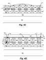
FIGS. 4A-D . FIGS. 4A-D illustrate cross sectional views of a portion of asubstrate 400 during fabrication of a first memory level in accordance with the present invention. As will be described below, the single memory level includes a plurality of memory cells that each include a reversible resistance-switching element formed using a selective growth process. Additional memory levels may be fabricated above the first memory level (as described previously with reference toFIGS. 2C-2D ).- With reference to
FIG. 4A , thesubstrate 400 is shown as having already undergone several processing steps. Thesubstrate 400 may be any suitable substrate such as a silicon, germanium, silicon-germanium, undoped, doped, bulk, silicon-on-insulator (SOI) or other substrate with or without additional circuitry. For example, thesubstrate 400 may include one or more n-well or p-well regions (not shown). Isolation layer 402 is formed above thesubstrate 400. In some embodiments, theisolation layer 402 may be a layer of silicon dioxide, silicon nitride, silicon oxynitride or any other suitable insulating layer. In other embodiments, theisolation layer 402 may be a shallow trench isolation (STI) region formed by etching a trench in thesubstrate 400, depositing a dielectric such as silicon dioxide, silicon nitride or another dielectric over thesubstrate 400 to fill the trench and planarizing thesubstrate 400 to re-expose atop surface 403 of thesubstrate 400. Note that in one or more embodiments, a silicon nitride or similar protective layer (not shown) may be formed over active regions (not shown) of thesubstrate 400 prior to isolation region formation (e.g., to protect the active regions). As an alternative, a localized oxidation of silicon (LOCOS) process or any other suitable process may be employed to define theisolation layer 402.- Following formation of the
isolation layer 402, anadhesion layer 404 is formed over the isolation layer402 (e.g., by physical vapor deposition or another method). For example, theadhesion layer 404 may be about 20 to about 500 angstroms, and preferably about 100 angstroms, of titanium nitride or another suitable adhesion layer such as tantalum nitride, tungsten nitride, combinations of one or more adhesion layers, or the like. Other adhesion layer materials and/or thicknesses may be employed. In some embodiments, theadhesion layer 404 may be optional. - After formation of the
adhesion layer 404, aconductive layer 406 is deposited over theadhesion layer 404. Theconductive layer 406 may include any suitable conductive material such as tungsten or another appropriate metal, heavily doped semiconductor material, a conductive silicide, a conductive silicide-germanide, a conductive germanide, or the like deposited by any suitable method (e.g., chemical vapor deposition, physical vapor deposition, etc.). In at least one embodiment, theconductive layer 406 may comprise about 200 to about 2500 angstroms of tungsten. Other conductive layer materials and/or thicknesses may be used. - After formation of the
conductive layer 406, a titanium-containinglayer 407, such as titanium nitride, is formed over the conductive layer406 (e.g., using physical vapor deposition or another method). In some embodiments, the titanium-containinglayer 407 includes about 20 to about 1200 angstroms of titanium nitride. Other titanium-containing layer materials, such as titanium, a titanium alloy, TiSi2, TiW, etc., and/or thicknesses may be used. - Following formation of the titanium-containing
layer 407, theadhesion layer 404, theconductive layer 406 and the titanium-containinglayer 407 are patterned and etched. For example, theadhesion layer 404, theconductive layer 406 and the titanium-containinglayer 407 may be patterned and etched using conventional lithography techniques, with a soft or hard mask, and wet or dry etch processing. In at least one embodiment, theadhesion layer 404, theconductive layer 406 and the titanium-containinglayer 407 are patterned and etched so as to form substantially parallel, substantially co-planar conductors408 (as shown inFIG. 4A ). Exemplary widths for theconductors 408 and/or spacings between theconductors 408 range from about 200 to about 2500 angstroms, although other conductor widths and/or spacings may be used. - After the
conductors 408 have been formed, adielectric layer 410 is deposited over thesubstrate 400 so as to fill the voids between theconductors 408. For example, approximately 3000-7000 angstroms of silicon dioxide may be deposited on thesubstrate 400 and planarized using chemical mechanical polishing or an etchback process to form aplanar surface 412. Theplanar surface 412 includes exposed,discrete regions 407a-fof titanium-containinglayer material 407 separated bydielectric material 410, as shown. The discrete titanium-containinglayer regions 407a-fmay be used to selectively form a titanium oxide reversible resistance-switching element for each memory cell being formed above the substrate400 (as described further below). - Other dielectric materials such as silicon nitride, silicon oxynitride, low K dielectrics, etc., and/or other dielectric layer thicknesses may be used. Exemplary low K dielectrics include carbon doped oxides, silicon carbon layers, or the like.
- If a reversible resistance-switching element is to be formed by oxidizing a material other than a titanium-containing material, the titanium-containing
layer 407 may be replaced with a layer of the material to be oxidized, such as Ta, TaN, Nb, NbN, Al, AlN, Hf, HfN, V, VN, etc. - Referring to
FIG. 4B , following planarization, a reversible resistance-switchingelement 413a-fis formed over each titanium-containinglayer region 407a-f. For example, a titanium oxide layer may be selectively formed over each titanium-containinglayer region 407a-fby oxidizing the titanium-containinglayer regions 407a-f. Some or all of each titanium-containinglayer region 407a-fmay be consumed during oxidation to create reversible resistance-switchingelements 413a-f. As described previously, any suitable method may be employed to oxidize the titanium-containinglayer regions 407a-fsuch as rapid thermal oxidation in an oxygen environment such as O2, ozone, a combination of the same, or using any other suitable oxidizing species. In other embodiments, a titanium-containing layer region may be oxidized using oxygen diffusion in a CVD chamber with an ozone or other oxygen source, using gaseous or liquid ozone cleaning, or using any other suitable oxidation process to form titanium oxide. - With reference to
FIG. 4C , after the reversible resistance-switchingelements 413a-fhave been formed, the diode structures of each memory cell are formed. An optional thin conductive layer (not shown), such as about 10 to about 300 angstroms of titanium, nickel, etc., may be formed over the titanium oxide layer regions (e.g., for work function tuning). In some embodiments, abarrier layer 414, such as titanium nitride, tantalum nitride, tungsten nitride, etc., may also be formed over the titanium oxide layer regions prior to diode formation (e.g., to prevent and/or reduce migration of metal atoms into the polysilicon regions). Thebarrier layer 414 may be on top of, in addition to or in place of the thin conductive layer and may be about 20 to about 500 angstroms, and preferably about 100 angstroms, of titanium nitride or another suitable barrier layer such as tantalum nitride, tungsten nitride, combinations of one or more barrier layers, barrier layers in combination with other layers such as titanium/titanium nitride, tantalum/tantalum nitride or tungsten/tungsten nitride stacks, or the like. Other barrier layer materials and/or thicknesses may be employed. - After deposition of the thin conductive layer (if used) and/or the
barrier layer 414, deposition of the semiconductor material used to form the diode of each memory cell begins (e.g.,diode 204 inFIGS. 2A-3 ). Each diode may be a vertical p-n or p-i-n diode as previously described. In some embodiments, each diode is formed from a polycrystalline semiconductor material such as polysilicon, a polysilicon-germanium alloy, germanium or any other suitable material. For convenience, formation of a polysilicon, downward-pointing diode is described herein. It will be understood that other materials and/or diode configurations may be used. - With reference to
FIG. 4C , following formation of thebarrier layer 414, a heavily dopedn+ silicon layer 416 is deposited on thebarrier layer 414. In some embodiments, then+ silicon layer 416 is in an amorphous state as deposited. In other embodiments, then+ silicon layer 416 is in a polycrystalline state as deposited. Chemical vapor deposition or another suitable process may be employed to deposit then+ silicon layer 416. In at least one embodiment, then+ silicon layer 416 may be formed, for example, from about 100 to about 1000 angstroms, preferably about 100 angstroms, of phosphorus or arsenic doped silicon having a doping concentration of about 1021 cm−3. Other layer thicknesses, dopants and/or doping concentrations may be used. Then+ silicon layer 416 may be doped in situ, for example, by flowing a donor gas during deposition. Other doping methods may be used (e.g., implantation). - After deposition of the
n+ silicon layer 416, a lightly doped, intrinsic and/or unintentionally dopedsilicon layer 418 is formed over then+ silicon layer 416. In some embodiments, theintrinsic silicon layer 418 is in an amorphous state as deposited. In other embodiments, theintrinsic silicon layer 418 is in a polycrystalline state as deposited. Chemical vapor deposition or another suitable deposition method may be employed to deposit theintrinsic silicon layer 418. In at least one embodiment, theintrinsic silicon layer 418 may be about 500 to about 4800 angstroms, preferably about 2500 angstroms, in thickness. Other intrinsic layer thicknesses may be used. - A thin (e.g., a few hundred angstroms or less) germanium and/or silicon-germanium alloy layer (not shown) may be formed on the
n+ silicon layer 416 prior to deposition of theintrinsic silicon layer 418 to prevent and/or reduce dopant migration from then+ silicon layer 416 into the intrinsic silicon layer418 (as described in the '331 application, previously incorporated). - Following formation of the
n+ silicon layer 416 and theintrinsic silicon layer 418, then+ silicon layer 416, theintrinsic silicon layer 418, thebarrier layer 414 and/or any conductive layer (if used) are patterned and etched so as to formsilicon pillars 420 overlying the conductors408 (as shown). Conventional lithography techniques, with a soft or hard mask, and wet or dry etch processing may be employed to form thesilicon pillars 420. - After the
silicon pillars 420 have been formed, adielectric layer 422 is deposited to fill the voids between thesilicon pillars 420. For example, approximately 200-7000 angstroms of silicon dioxide may be deposited and planarized using chemical mechanical polishing or an etchback process to form aplanar surface 424. Theplanar surface 424 includes exposed top surfaces of thesilicon pillars 420 separated bydielectric material 422, as shown. Other dielectric materials such as silicon nitride, silicon oxynitride, low K dielectrics, etc., and/or other dielectric layer thicknesses may be used. Exemplary low K dielectrics include carbon doped oxides, silicon carbon layers, or the like. - After formation of the
silicon pillars 420, ap+ silicon region 426 is formed within eachsilicon pillar 420, near the upper surface of thesilicon pillars 420. For example, a blanket p+ implant may be employed to implant boron a predetermined depth within thesilicon pillars 420. Exemplary implantable molecular ions include BF2, BF3, B and the like. In some embodiments, an implant dose of about 1-5×10¹⁵ions/cm2may be employed. Other implant species and/or doses may be used. Further, in some embodiments, a diffusion process may be employed to dope the upper portion of thesilicon pillars 420. In at least one embodiment, thep+ silicon regions 426 have a depth of about 100-700 angstroms, although other p+ silicon region sizes may be used. (Note that if the diodes to be formed are upward pointing p-n or p-i-n diodes, the upper portion of thesilicon pillars 420 will be doped n-type). Eachsilicon pillar 420 thereby includes a downward-pointing,p-i-n diode 428. - With reference to
FIG. 4D , after completion of thep-i-n diodes 428, a silicide-formingmetal layer 430 is deposited over thesubstrate 400. Exemplary silicide-forming metals include sputter or otherwise deposited titanium or cobalt. In some embodiments, the silicide-formingmetal layer 430 has a thickness of about 10 to about 200 angstroms, preferably about 20 to about 50 angstroms and more preferably about 20 angstroms. Other silicide-forming metal layer materials and/or thicknesses may be used. As will be described further below, annealing of the structure causes metal from the silicide-formingmetal layer 430 and silicon from thep+ silicon regions 426 to react to form asilicide region 432 adjacent eachp+ silicon region 426. - Following formation of the silicide-forming
metal layer 430, a second set ofconductors 436 may be formed above thediodes 428 in a manner similar to the formation of the bottom set ofconductors 408. In some embodiments, one or more barrier layers and/oradhesion layers 438 may be placed over the silicide-formingmetal layer 430 prior to deposition of aconductive layer 440 used to form the upper, second set ofconductors 436. - The
conductive layer 440 may be formed from any suitable conductive material such as tungsten, another suitable metal, heavily doped semiconductor material, a conductive silicide, a conductive silicide-germanide, a conductive germanide, or the like deposited by any suitable method (e.g., chemical vapor deposition, physical vapor deposition, etc.). Other conductive layer materials may be used. Barrier layers and/oradhesion layers 438 may include titanium nitride or another suitable layer such as tantalum nitride, tungsten nitride, combinations of one or more layers, or any other suitable material(s). The depositedconductive layer 440, barrier and/oradhesion layer 438, and/or silicide-formingmetal layer 430 may be patterned and/or etched to form the second set ofconductors 436. In at least one embodiment, theupper conductors 436 are substantially parallel, substantially coplanar conductors that extend in a different direction than thelower conductors 408. - Following formation of the
upper conductors 436, the structure may be annealed to crystallize the deposited semiconductor material of the diodes428 (and/or to form the silicide regions432). In at least one embodiment, the anneal may be performed for about 10 seconds to about 2 minutes in nitrogen at a temperature of about 600 to 800° C., and more preferably between about 650 and 750° C. Other annealing times, temperatures and/or environments may be used. Thesilicide regions 432 may serve as “crystallization templates” or “seeds” during annealing for underlying deposited semiconductor material that forms the diodes432 (e.g., changing any amorphous semiconductor material to polycrystalline semiconductor material and/or improving overall crystalline properties of the diodes432). Lower resistivity diode material thereby is provided. FIG. 5 is a cross sectional view of anexemplary memory cell 500 provided in accordance with the present invention. Thememory cell 500 includes a thin film transistor (TFT), such as a thin film, metal oxide semiconductor field effect transistor (MOSFET)502 coupled to a reversible resistance-switchingelement 504 formed above asubstrate 505. For example, theMOSFET 502 may be an n-channel or a p-channel thin film MOSFET formed on any suitable substrate. In the embodiment shown, aninsulating region 506 such as silicon dioxide, silicon nitride, oxynitride, etc., is formed above thesubstrate 505 and a depositedsemiconductor region 507 such as deposited silicon, germanium, silicon-germanium, etc., is formed above theinsulating region 506. Thethin film MOSFET 502 is formed within the depositedsemiconductor region 507 and is insulated from thesubstrate 505 by theinsulating region 506.- The
MOSFET 502 includes source/drain regions channel region 512, as well asgate dielectric layer 514,gate electrode 516 and spacers518a-b. In at least one embodiment, the source/drain regions channel region 512 may be doped n-type, while in other embodiments the source/drain regions channel region 512 may be doped p-type. Any other MOSFET configuration or any suitable fabrication techniques may be employed for thethin film MOSFET 502. In some embodiments, theMOSFET 502 may be electrically isolated by isolation regions (not shown) formed in the substrate506 (e.g., formed using an STI, LOCOS or other similar process). Alternatively, gate, source and/or drain regions of theMOSFET 502 may be shared with other transistors (not shown) formed on thesubstrate 506. - The reversible resistance-switching
element 504 includes alower conductor 520, a titanium-containinglayer 521 formed over thelower conductor 520, atitanium oxide layer 522 selectively grown over the titanium-containinglayer 521 and anupper conductor 524 formed over the reversible resistivity-switching material (titanium oxide layer522). The upper andlower conductors lower conductors - In at least one embodiment, the reversible resistivity-switching material (titanium oxide layer522) is formed using a selective growth process as previously described with reference to the embodiments of
FIGS. 1-4D . For example, thetitanium oxide layer 522 may be selectively formed by rapid thermal oxidation of the titanium-containinglayer 521 in an oxygen environment such as O2, ozone, a combination of the same, or using any other suitable oxidizing species. In other embodiments, thetitanium oxide layer 522 may be formed by oxidizing the titanium-containinglayer 521 using oxygen diffusion in a chemical vapor deposition (CVD) chamber with an ozone or other oxygen source, using gaseous or liquid ozone cleaning, or using any other suitable oxidation process. In any case, the need for etching of titanium oxide layers may be eliminated and memory cell fabrication significantly simplified. Other materials may be selectively oxidized in accordance with the present invention to form reversible resistivity-switching materials for use in memory cell500 (e.g., Ta, TaN, Nb, NbN, Al, AlN, Hf, HfN, V, VN, etc.). - As shown in
FIG. 5 , the reversible resistance-switchingelement 504 is coupled to the source/drain region 510 of theMOSFET 502 by a firstconductive plug 526 and to a first metal level (M1)line 528 by a second conductive plug530 (which extend through a dielectric layer532). Likewise, a thirdconductive plug 534 couples the source/drain region 508 of theMOSFET 502 to anM1 line 536. The conductive plugs and/or lines may be formed from any suitable materials (without or without barriers layers) such as tungsten, another metal, heavily doped semiconductor material, a conductive silicide, a conductive silicide-germanide, a conductive germanide, or the like. Note that when theMOSFET 502 is an n-channel device, theregion 508 serves as the drain and theregion 510 serves as the source for theMOSFET 502; and when theMOSFET 502 is an p-channel device, theregion 508 serves as the source and theregion 510 serves as the drain for theMOSFET 502. Thedielectric layer 532 may include any suitable dielectric such as silicon dioxide, silicon nitride, silicon oxynitride, low K dielectrics, etc. - In the
memory cell 500, thethin film MOSFET 502 operates as a steering element in a manner similar to that of the diodes employed in the memory cells ofFIGS. 2A-4D , selectively limiting the voltage applied across and/or the current flow through the reversible resistance-switchingelement 504. - In at least one embodiment, the reversible resistance-switching
element 504 includes a titanium oxide layer having a thickness of about 500 angstroms or less, and more preferably a thickness of about 300 angstroms or less. Other titanium oxide thicknesses may be employed. - The foregoing description discloses only exemplary embodiments of the invention. Modifications of the above disclosed apparatus and methods which fall within the scope of the invention will be readily apparent to those of ordinary skill in the art. For instance, although the present invention has been described primarily with regard to selective oxidation of titanium nitride, it will be understood that other materials may be selectively oxidized to form reversible resistivity-switching materials for use in memory cells such as Ta, TaN, Nb, NbN, Al, AlN, Hf, HfN, V, VN, etc.
- Accordingly, while the present invention has been disclosed in connection with exemplary embodiments thereof, it should be understood that other embodiments may fall within the spirit and scope of the invention, as defined by the following claims.
Claims (40)
Priority Applications (10)
| Application Number | Priority Date | Filing Date | Title |
|---|---|---|---|
| US11/772,088US7902537B2 (en) | 2007-06-29 | 2007-06-29 | Memory cell that employs a selectively grown reversible resistance-switching element and methods of forming the same |
| CN201210124956.3ACN102709471B (en) | 2007-06-29 | 2008-06-27 | Memory cell that employs a selectively grown reversible resistance-switching element and methods of forming the same |
| TW097124406ATW200915543A (en) | 2007-06-29 | 2008-06-27 | Memory cell that employs a selectively grown reversible resistance-switching element and methods of forming the same |
| PCT/US2008/007985WO2009005699A1 (en) | 2007-06-29 | 2008-06-27 | Memory cell that employs a selectively grown reversible resistance-switching element and methods of forming the same |
| CN2008800226674ACN101720508B (en) | 2007-06-29 | 2008-06-27 | Memory cell utilizing selectively grown reversible resistance-switching element and method of forming same |
| KR1020097027300AKR20100031698A (en) | 2007-06-29 | 2008-06-27 | Memory cell that employs a selectively grown reversible resistance-switching element and methods of forming the same |
| EP08768806AEP2162917A1 (en) | 2007-06-29 | 2008-06-27 | Memory cell that employs a selectively grown reversible resistance-switching element and methods of forming the same |
| JP2010514823AJP2010532568A (en) | 2007-06-29 | 2008-06-27 | Memory cell using reversible resistance switching element by selective growth and formation method thereof |
| US13/037,591US8373150B2 (en) | 2007-06-29 | 2011-03-01 | Memory cell that employs a selectively grown reversible resistance-switching element and methods of forming the same |
| US13/764,065US8816315B2 (en) | 2007-06-29 | 2013-02-11 | Memory cell that employs a selectively grown reversible resistance-switching element and methods of forming the same |
Applications Claiming Priority (1)
| Application Number | Priority Date | Filing Date | Title |
|---|---|---|---|
| US11/772,088US7902537B2 (en) | 2007-06-29 | 2007-06-29 | Memory cell that employs a selectively grown reversible resistance-switching element and methods of forming the same |
Related Child Applications (1)
| Application Number | Title | Priority Date | Filing Date |
|---|---|---|---|
| US13/037,591ContinuationUS8373150B2 (en) | 2007-06-29 | 2011-03-01 | Memory cell that employs a selectively grown reversible resistance-switching element and methods of forming the same |
Publications (2)
| Publication Number | Publication Date |
|---|---|
| US20090001344A1true US20090001344A1 (en) | 2009-01-01 |
| US7902537B2 US7902537B2 (en) | 2011-03-08 |
Family
ID=40159270
Family Applications (3)
| Application Number | Title | Priority Date | Filing Date |
|---|---|---|---|
| US11/772,088Expired - Fee RelatedUS7902537B2 (en) | 2007-06-29 | 2007-06-29 | Memory cell that employs a selectively grown reversible resistance-switching element and methods of forming the same |
| US13/037,591Expired - Fee RelatedUS8373150B2 (en) | 2007-06-29 | 2011-03-01 | Memory cell that employs a selectively grown reversible resistance-switching element and methods of forming the same |
| US13/764,065ActiveUS8816315B2 (en) | 2007-06-29 | 2013-02-11 | Memory cell that employs a selectively grown reversible resistance-switching element and methods of forming the same |
Family Applications After (2)
| Application Number | Title | Priority Date | Filing Date |
|---|---|---|---|
| US13/037,591Expired - Fee RelatedUS8373150B2 (en) | 2007-06-29 | 2011-03-01 | Memory cell that employs a selectively grown reversible resistance-switching element and methods of forming the same |
| US13/764,065ActiveUS8816315B2 (en) | 2007-06-29 | 2013-02-11 | Memory cell that employs a selectively grown reversible resistance-switching element and methods of forming the same |
Country Status (1)
| Country | Link |
|---|---|
| US (3) | US7902537B2 (en) |
Cited By (46)
| Publication number | Priority date | Publication date | Assignee | Title |
|---|---|---|---|---|
| US20060250837A1 (en)* | 2005-05-09 | 2006-11-09 | Sandisk 3D, Llc | Nonvolatile memory cell comprising a diode and a resistance-switching material |
| US20070114509A1 (en)* | 2005-11-23 | 2007-05-24 | Sandisk 3D Llc | Memory cell comprising nickel-cobalt oxide switching element |
| US20070228414A1 (en)* | 2006-03-31 | 2007-10-04 | Sandisk 3D, Llc | Heterojunction device comprising a semiconductor and a resistivity-switching oxide or nitride |
| US20070236981A1 (en)* | 2006-03-31 | 2007-10-11 | Sandisk 3D, Llc | Multilevel nonvolatile memory cell comprising a resistivity-switching oxide or nitride and an antifuse |
| US20090001345A1 (en)* | 2007-06-29 | 2009-01-01 | April Schricker | Memory cell that employs a selectively deposited reversible resistance-switching element and methods of forming the same |
| US20090001342A1 (en)* | 2007-06-29 | 2009-01-01 | April Schricker | Memory cell that employs a selectively grown reversible resistance-switching element and methods of forming the same |
| US20090001343A1 (en)* | 2007-06-29 | 2009-01-01 | April Schricker | Memory cell that employs a selectively deposited reversible resistance-switching element and methods of forming the same |
| US20100259960A1 (en)* | 2009-04-08 | 2010-10-14 | George Samachisa | Three-Dimensional Array of Re-Programmable Non-Volatile Memory Elements Having Vertical Bit Lines |
| US20100259962A1 (en)* | 2009-04-08 | 2010-10-14 | Tianhong Yan | Three-Dimensional Array of Re-Programmable Non-Volatile Memory Elements Having Vertical Bit Lines and a Single-Sided Word Line Architecture |
| WO2010117914A1 (en) | 2009-04-08 | 2010-10-14 | Sandisk 3D Llc | Three-dimensional array of re-programmable non-volatile memory elements having vertical bit lines and a single-sided word line architecture |
| US20100259961A1 (en)* | 2009-04-08 | 2010-10-14 | Luca Fasoli | Three-Dimensional Array of Re-Programmable Non-Volatile Memory Elements Having Vertical Bit Lines and a Double-Global-Bit-Line Architecture |
| US7816659B2 (en) | 2005-11-23 | 2010-10-19 | Sandisk 3D Llc | Devices having reversible resistivity-switching metal oxide or nitride layer with added metal |
| US7829875B2 (en) | 2006-03-31 | 2010-11-09 | Sandisk 3D Llc | Nonvolatile rewritable memory cell comprising a resistivity-switching oxide or nitride and an antifuse |
| US20110147693A1 (en)* | 2007-06-29 | 2011-06-23 | April Schricker | Memory cell that employs a selectively grown reversible resistance-switching element and methods of forming the same |
| WO2011156343A2 (en) | 2010-06-08 | 2011-12-15 | Sandisk 3D Llc | Non-volatile memory having 3d array of read/write elements and read/write circuits and method thereof |
| WO2011156357A1 (en) | 2010-06-08 | 2011-12-15 | Sandisk 3D Llc | Non-volatile memory having 3d array of read/write elements with efficient decoding of vertical bit lines and word lines |
| WO2012082775A1 (en) | 2010-12-14 | 2012-06-21 | Sandisk 3D Llc | Non-volatile memory having 3d array of read/write elements with vertical bit lines and select devices and methods thereof |
| WO2012082654A2 (en) | 2010-12-14 | 2012-06-21 | Sandisk 3D Llc | Architecture for three dimesional non-volatile storage with vertical bit lines |
| WO2013101499A2 (en) | 2011-12-30 | 2013-07-04 | SanDisk Technologies, Inc. | Low forming voltage non-volatile storage device |
| WO2013173140A2 (en) | 2012-05-15 | 2013-11-21 | SanDisk Technologies, Inc. | Three dimensional non-volatile storage with interleaved vertical select devices above and below vertical bit lines |
| WO2013188563A1 (en) | 2012-06-15 | 2013-12-19 | Sandisk 3D Llc | Non-volatile memory having 3d array architecture with staircase word lines and vertical bit lines and methods thereof |
| WO2013192216A2 (en) | 2012-06-21 | 2013-12-27 | Sandisk 3D Llc | Memories with cylindrical read/write stacks |
| US20140001431A1 (en)* | 2008-05-01 | 2014-01-02 | Intermolecular Inc. | Reduction of forming voltage in semiconductor devices |
| WO2014138182A1 (en) | 2013-03-05 | 2014-09-12 | Sandisk 3D Llc | 3d non-volatile memory having low-current cells and fabrication thereof |
| US8916872B1 (en) | 2014-07-11 | 2014-12-23 | Inoso, Llc | Method of forming a stacked low temperature diode and related devices |
| WO2015085106A1 (en) | 2013-12-06 | 2015-06-11 | Sandisk 3D Llc | Method of forming insulated sidewall gate electrode for vertical field effect transistor |
| US9087689B1 (en) | 2014-07-11 | 2015-07-21 | Inoso, Llc | Method of forming a stacked low temperature transistor and related devices |
| US9123392B1 (en) | 2014-03-28 | 2015-09-01 | Sandisk 3D Llc | Non-volatile 3D memory with cell-selectable word line decoding |
| WO2015138314A1 (en) | 2014-03-12 | 2015-09-17 | Sandisk 3D Llc | Vertical field effect transistor device and method of making thereof |
| WO2015148299A1 (en) | 2014-03-25 | 2015-10-01 | Sandisk 3D Llc | Transistor device with gate bottom isolation and method of making thereof |
| US9165933B2 (en) | 2013-03-07 | 2015-10-20 | Sandisk 3D Llc | Vertical bit line TFT decoder for high voltage operation |
| US9202694B2 (en) | 2013-03-04 | 2015-12-01 | Sandisk 3D Llc | Vertical bit line non-volatile memory systems and methods of fabrication |
| WO2016022304A1 (en) | 2014-08-05 | 2016-02-11 | Sandisk 3D Llc | Fully isolated selector for memory device |
| WO2016028484A1 (en) | 2014-08-19 | 2016-02-25 | Sandisk 3D Llc | Word line connection for memory device and method of making thereof |
| US9281029B2 (en) | 2012-06-15 | 2016-03-08 | Sandisk 3D Llc | Non-volatile memory having 3D array architecture with bit line voltage control and methods thereof |
| US9362338B2 (en) | 2014-03-03 | 2016-06-07 | Sandisk Technologies Inc. | Vertical thin film transistors in non-volatile storage systems |
| US9379246B2 (en) | 2014-03-05 | 2016-06-28 | Sandisk Technologies Inc. | Vertical thin film transistor selection devices and methods of fabrication |
| WO2016126307A1 (en) | 2015-02-05 | 2016-08-11 | Sandisk Technologies, Llc | Memory device with comb electrode and method of making thereof |
| US9627009B2 (en) | 2014-07-25 | 2017-04-18 | Sandisk Technologies Llc | Interleaved grouped word lines for three dimensional non-volatile storage |
| US9698202B2 (en) | 2015-03-02 | 2017-07-04 | Sandisk Technologies Llc | Parallel bit line three-dimensional resistive random access memory |
| US9704920B2 (en) | 2015-10-27 | 2017-07-11 | Sandisk Technologies Llc | Resistive random access memory containing a steering element and a tunneling dielectric element |
| US9805805B1 (en) | 2016-08-23 | 2017-10-31 | Sandisk Technologies Llc | Three-dimensional memory device with charge carrier injection wells for vertical channels and method of making and using thereof |
| US9812505B2 (en) | 2015-11-16 | 2017-11-07 | Sandisk Technologies Llc | Non-volatile memory device containing oxygen-scavenging material portions and method of making thereof |
| US10157681B2 (en) | 2015-09-14 | 2018-12-18 | Sandisk Technologies Llc | Programming of nonvolatile memory with verify level dependent on memory state and programming loop count |
| US10410717B2 (en)* | 2016-03-07 | 2019-09-10 | Toshiba Memory Corporation | Resistive random access memory device with three-dimensional cross-point structure and method of operating the same |
| US20200295038A1 (en)* | 2019-03-11 | 2020-09-17 | Toshiba Memory Corporation | Voltage-variable type memory element and semiconductor memory device having the same |
Families Citing this family (6)
| Publication number | Priority date | Publication date | Assignee | Title |
|---|---|---|---|---|
| US8000127B2 (en)* | 2009-08-12 | 2011-08-16 | Nantero, Inc. | Method for resetting a resistive change memory element |
| US9263126B1 (en) | 2010-09-01 | 2016-02-16 | Nantero Inc. | Method for dynamically accessing and programming resistive change element arrays |
| KR20100130419A (en)* | 2009-06-03 | 2010-12-13 | 삼성전자주식회사 | Heterojunction diode, manufacturing method thereof, and electronic device including heterojunction diode |
| KR20110101983A (en)* | 2010-03-10 | 2011-09-16 | 삼성전자주식회사 | Bipolar memory cell and memory device including same |
| US8933516B1 (en) | 2013-06-24 | 2015-01-13 | Sandisk 3D Llc | High capacity select switches for three-dimensional structures |
| US11042432B1 (en) | 2019-12-20 | 2021-06-22 | Western Digital Technologies, Inc. | Data storage device with dynamic stripe length manager |
Citations (91)
| Publication number | Priority date | Publication date | Assignee | Title |
|---|---|---|---|---|
| US2655609A (en)* | 1952-07-22 | 1953-10-13 | Bell Telephone Labor Inc | Bistable circuits, including transistors |
| US2971140A (en)* | 1959-01-07 | 1961-02-07 | Marc A Chappey | Two-terminal semi-conductor devices having negative differential resistance |
| US3796926A (en)* | 1971-03-29 | 1974-03-12 | Ibm | Bistable resistance device which does not require forming |
| US4204028A (en)* | 1978-03-16 | 1980-05-20 | Ppg Industries, Inc. | Conductive metal oxide film for solar energy control |
| US4465370A (en)* | 1980-07-01 | 1984-08-14 | Minolta Camera Kabushiki Kaisha | Light measuring device |
| US4499557A (en)* | 1980-10-28 | 1985-02-12 | Energy Conversion Devices, Inc. | Programmable cell for use in programmable electronic arrays |
| US4646266A (en)* | 1984-09-28 | 1987-02-24 | Energy Conversion Devices, Inc. | Programmable semiconductor structures and methods for using the same |
| US4772571A (en)* | 1984-09-14 | 1988-09-20 | Stc Plc | Process of self aligned nitridation of TiSi2 to form TiN/TiSi2 contact |
| US4907054A (en)* | 1987-11-10 | 1990-03-06 | Thomson-Csf | Matrix of photosensitive elements combining a phototransistor with a storage capacitor |
| US4940553A (en)* | 1988-05-26 | 1990-07-10 | Deutsche Automobilgesellschaft | Aqueous nickel hydroxide paste of high flowability |
| US5037200A (en)* | 1989-07-11 | 1991-08-06 | Tosoh Corporation | Laser-operated detector |
| US5166758A (en)* | 1991-01-18 | 1992-11-24 | Energy Conversion Devices, Inc. | Electrically erasable phase change memory |
| US5311055A (en)* | 1991-11-22 | 1994-05-10 | The United States Of America As Represented By The Secretary Of The Navy | Trenched bipolar transistor structures |
| US5774394A (en)* | 1997-05-22 | 1998-06-30 | Motorola, Inc. | Magnetic memory cell with increased GMR ratio |
| US5876788A (en)* | 1997-01-16 | 1999-03-02 | International Business Machines Corporation | High dielectric TiO2 -SiN composite films for memory applications |
| US5915167A (en)* | 1997-04-04 | 1999-06-22 | Elm Technology Corporation | Three dimensional structure memory |
| US6034882A (en)* | 1998-11-16 | 2000-03-07 | Matrix Semiconductor, Inc. | Vertically stacked field programmable nonvolatile memory and method of fabrication |
| USRE37259E1 (en)* | 1996-04-19 | 2001-07-03 | Energy Conversion Devices, Inc. | Multibit single cell memory element having tapered contact |
| US6369431B1 (en)* | 1996-02-23 | 2002-04-09 | Micron Technology, Inc. | Method for forming conductors in semiconductor devices |
| US20020057594A1 (en)* | 2000-11-01 | 2002-05-16 | Tadahiko Hirai | Magnetic memory and information recording and reproducing method therefor |
| US6426891B1 (en)* | 1999-10-27 | 2002-07-30 | Sony Corporation | Nonvolatile memory with a two-terminal switching element and its driving method |
| US6483734B1 (en)* | 2001-11-26 | 2002-11-19 | Hewlett Packard Company | Memory device having memory cells capable of four states |
| US20030013007A1 (en)* | 2001-07-13 | 2003-01-16 | Kaun Thomas D. | Cell structure for electrochemical devices and method of making same |
| US20030047727A1 (en)* | 2001-09-07 | 2003-03-13 | Chien Chiang | Using selective deposition to form phase-change memory cells |
| US6534841B1 (en)* | 2001-12-14 | 2003-03-18 | Hewlett-Packard Company | Continuous antifuse material in memory structure |
| US6541792B1 (en)* | 2001-09-14 | 2003-04-01 | Hewlett-Packard Development Company, Llp | Memory device having dual tunnel junction memory cells |
| US20030081446A1 (en)* | 2001-10-31 | 2003-05-01 | Peter Fricke | Memory cell structure |
| US20030209971A1 (en)* | 2000-02-11 | 2003-11-13 | Kozicki Michael N. | Programmable structure, an array including the structure, and methods of forming the same |
| US20040002186A1 (en)* | 2002-06-27 | 2004-01-01 | Vyvoda Michael A. | Electrically isolated pillars in active devices |
| US20040084743A1 (en)* | 2002-11-04 | 2004-05-06 | Vanbuskirk Michael A. | Control of memory arrays utilizing zener diode-like devices |
| US20040095300A1 (en)* | 2002-11-20 | 2004-05-20 | Osram Opto Semiconductors Gmbh | Current limiting device |
| US6753561B1 (en)* | 2002-08-02 | 2004-06-22 | Unity Semiconductor Corporation | Cross point memory array using multiple thin films |
| US6761985B2 (en)* | 2000-10-05 | 2004-07-13 | Battelle Memorial Institute | Magnetic transparent conducting oxide film and method of making |
| US6774458B2 (en)* | 2002-07-23 | 2004-08-10 | Hewlett Packard Development Company, L.P. | Vertical interconnection structure and methods |
| US6778441B2 (en)* | 2001-08-30 | 2004-08-17 | Micron Technology, Inc. | Integrated circuit memory device and method |
| US20040160818A1 (en)* | 2002-08-02 | 2004-08-19 | Unity Semiconductor Corporation | Cross point memory array using multiple modes of operation |
| US20040159828A1 (en)* | 2002-08-02 | 2004-08-19 | Unity Semiconductor, Inc. | Resistive memory device with a treated interface |
| US20040160808A1 (en)* | 2002-08-02 | 2004-08-19 | Unity Semiconductor Corporation | Cross point memory array using distinct voltages |
| US20040160798A1 (en)* | 2002-10-31 | 2004-08-19 | Unity Semiconductor Inc. | Adaptive programming technique for a re-writable conductive memory device |
| US20040160807A1 (en)* | 2002-08-02 | 2004-08-19 | Unity Semiconductor Corporation | Cross point memory array with memory plugs exhibiting a characteristic hysteresis |
| US20040161888A1 (en)* | 2002-08-02 | 2004-08-19 | Unity Semiconductor Corporation | Multi-resistive state material that uses dopants |
| US20040160812A1 (en)* | 2002-08-02 | 2004-08-19 | Unity Semiconductor Corporation | 2-Terminal trapped charge memory device with voltage switchable multi-level resistance |
| US20040159867A1 (en)* | 2002-08-02 | 2004-08-19 | Unity Semiconductor Corporation | Multi-layer conductive memory device |
| US20040160805A1 (en)* | 2002-08-02 | 2004-08-19 | Unity Semiconductor Corporation | Multi-output multiplexor |
| US20040160819A1 (en)* | 2002-08-02 | 2004-08-19 | Unity Semiconductor Corporation | High-density NVRAM |
| US20040160817A1 (en)* | 2002-08-02 | 2004-08-19 | Unity Semiconductor Corporation | Non-volatile memory with a single transistor and resistive memory element |
| US20040159869A1 (en)* | 2002-08-02 | 2004-08-19 | Unity Semiconductor Corporation | Memory array with high temperature wiring |
| US20040160804A1 (en)* | 2002-08-02 | 2004-08-19 | Unity Semiconductor Corporation | Memory array of a non-volatile ram |
| US20040160806A1 (en)* | 2002-08-02 | 2004-08-19 | Unity Semiconductor Corporation | Providing a reference voltage to a cross point memory array |
| US20040170040A1 (en)* | 2002-08-02 | 2004-09-02 | Unity Semiconductor Corporation | Rewritable memory with non-linear memory element |
| US6787401B2 (en)* | 1996-03-01 | 2004-09-07 | Micron Technology, Inc. | Method of making vertical diode structures |
| US6815744B1 (en)* | 1999-02-17 | 2004-11-09 | International Business Machines Corporation | Microelectronic device for storing information with switchable ohmic resistance |
| US20040228172A1 (en)* | 2002-08-02 | 2004-11-18 | Unity Semiconductor Corporation | Conductive memory stack with sidewall |
| US6850455B2 (en)* | 2002-08-02 | 2005-02-01 | Unity Semiconductor Corporation | Multiplexor having a reference voltage on unselected lines |
| US20050045919A1 (en)* | 2003-08-27 | 2005-03-03 | Nec Corporation | Semiconductor device |
| US20050058009A1 (en)* | 2003-09-03 | 2005-03-17 | Yang Yang | Memory devices based on electric field programmable films |
| US20050167699A1 (en)* | 2003-10-23 | 2005-08-04 | Matsushita Electric Industrial Co., Ltd. | Variable resistance element, method of manufacturing the element, memory containing the element, and method of driving the memory |
| US6946719B2 (en)* | 2003-12-03 | 2005-09-20 | Matrix Semiconductor, Inc | Semiconductor device including junction diode contacting contact-antifuse unit comprising silicide |
| US6952030B2 (en)* | 2002-12-19 | 2005-10-04 | Matrix Semiconductor, Inc. | High-density three-dimensional memory cell |
| US20050247921A1 (en)* | 2004-04-28 | 2005-11-10 | Samsung Electronics Co., Ltd. | Memory device using multi-layer with a graded resistance change |
| US20060006495A1 (en)* | 2002-12-19 | 2006-01-12 | Matrix Semiconductor, Inc. | Ultrathin chemically grown oxide film as a dopant diffusion barrier in semiconductor devices |
| US20060067117A1 (en)* | 2004-09-29 | 2006-03-30 | Matrix Semiconductor, Inc. | Fuse memory cell comprising a diode, the diode serving as the fuse element |
| US20060094236A1 (en)* | 2004-11-03 | 2006-05-04 | Elkins Patricia C | Electroless plating of metal caps for chalcogenide-based memory devices |
| US20060098472A1 (en)* | 2004-11-10 | 2006-05-11 | Seung-Eon Ahn | Nonvolatile memory device, array of nonvolatile memory devices, and methods of making the same |
| US20060128153A1 (en)* | 2004-12-14 | 2006-06-15 | Matrix Semiconductor, Inc. | Method for cleaning slurry particles from a surface polished by chemical mechanical polishing |
| US20060157679A1 (en)* | 2005-01-19 | 2006-07-20 | Matrix Semiconductor, Inc. | Structure and method for biasing phase change memory array for reliable writing |
| US20060164880A1 (en)* | 2003-07-18 | 2006-07-27 | Toshitsugu Sakamoto | Switching element method of driving switching element rewritable logic integrated circuit and memory |
| US20060250836A1 (en)* | 2005-05-09 | 2006-11-09 | Matrix Semiconductor, Inc. | Rewriteable memory cell comprising a diode and a resistance-switching material |
| US20060250837A1 (en)* | 2005-05-09 | 2006-11-09 | Sandisk 3D, Llc | Nonvolatile memory cell comprising a diode and a resistance-switching material |
| US20070010100A1 (en)* | 2005-07-11 | 2007-01-11 | Matrix Semiconductor, Inc. | Method of plasma etching transition metals and their compounds |
| US7176064B2 (en)* | 2003-12-03 | 2007-02-13 | Sandisk 3D Llc | Memory cell comprising a semiconductor junction diode crystallized adjacent to a silicide |
| US20070072360A1 (en)* | 2005-09-28 | 2007-03-29 | Tanmay Kumar | Method for using a memory cell comprising switchable semiconductor memory element with trimmable resistance |
| US7215564B2 (en)* | 2004-04-27 | 2007-05-08 | Infineon Technologies Ag | Semiconductor memory component in cross-point architecture |
| US20070114508A1 (en)* | 2005-11-23 | 2007-05-24 | Matrix Semiconductor, Inc. | Reversible resistivity-switching metal oxide or nitride layer with added metal |
| US20070114509A1 (en)* | 2005-11-23 | 2007-05-24 | Sandisk 3D Llc | Memory cell comprising nickel-cobalt oxide switching element |
| US7224013B2 (en)* | 2004-09-29 | 2007-05-29 | Sandisk 3D Llc | Junction diode comprising varying semiconductor compositions |
| US7238607B2 (en)* | 2002-12-19 | 2007-07-03 | Sandisk 3D Llc | Method to minimize formation of recess at surface planarized by chemical mechanical planarization |
| US20070190722A1 (en)* | 2002-12-19 | 2007-08-16 | Herner S B | Method to form upward pointing p-i-n diodes having large and uniform current |
| US20070228354A1 (en)* | 2006-03-31 | 2007-10-04 | Sandisk 3D, Llc | Nonvolatile rewritable memory cell comprising a resistivity-switching oxide or nitride and an antifuse |
| US20070228414A1 (en)* | 2006-03-31 | 2007-10-04 | Sandisk 3D, Llc | Heterojunction device comprising a semiconductor and a resistivity-switching oxide or nitride |
| US20070236981A1 (en)* | 2006-03-31 | 2007-10-11 | Sandisk 3D, Llc | Multilevel nonvolatile memory cell comprising a resistivity-switching oxide or nitride and an antifuse |
| US20070246743A1 (en)* | 2006-04-21 | 2007-10-25 | Sung-Lae Cho | Method of forming a phase change material layer, method of forming a phase change memory device using the same, and a phase change memory device so formed |
| US7391064B1 (en)* | 2004-12-01 | 2008-06-24 | Spansion Llc | Memory device with a selection element and a control line in a substantially similar layer |
| US20080175032A1 (en)* | 2007-01-23 | 2008-07-24 | Kabushiki Kaisha Toshiba | Semiconductor memory and method for manufacturing the same |
| US7405465B2 (en)* | 2004-09-29 | 2008-07-29 | Sandisk 3D Llc | Deposited semiconductor structure to minimize n-type dopant diffusion and method of making |
| US20090001343A1 (en)* | 2007-06-29 | 2009-01-01 | April Schricker | Memory cell that employs a selectively deposited reversible resistance-switching element and methods of forming the same |
| US20090001345A1 (en)* | 2007-06-29 | 2009-01-01 | April Schricker | Memory cell that employs a selectively deposited reversible resistance-switching element and methods of forming the same |
| US20090001342A1 (en)* | 2007-06-29 | 2009-01-01 | April Schricker | Memory cell that employs a selectively grown reversible resistance-switching element and methods of forming the same |
| US7501331B2 (en)* | 2006-03-31 | 2009-03-10 | Sandisk 3D Llc | Low-temperature metal-induced crystallization of silicon-germanium films |
| US20090104756A1 (en)* | 2007-06-29 | 2009-04-23 | Tanmay Kumar | Method to form a rewriteable memory cell comprising a diode and a resistivity-switching grown oxide |
| US20090236581A1 (en)* | 2006-11-30 | 2009-09-24 | Fujitsu Limited | Resistance memory element, method of manufacturing resistance memory element and semiconductor memory device |
Family Cites Families (39)
| Publication number | Priority date | Publication date | Assignee | Title |
|---|---|---|---|---|
| GB1284645A (en) | 1970-01-30 | 1972-08-09 | Welwyn Electric Ltd | Then film device |
| US3717852A (en)* | 1971-09-17 | 1973-02-20 | Ibm | Electronically rewritable read-only memory using via connections |
| US3795977A (en)* | 1971-12-30 | 1974-03-12 | Ibm | Methods for fabricating bistable resistors |
| IT982622B (en) | 1972-06-05 | 1974-10-21 | Ibm | PERFECTED STORAGE DEVICE |
| US4203123A (en)* | 1977-12-12 | 1980-05-13 | Burroughs Corporation | Thin film memory device employing amorphous semiconductor materials |
| US5075738A (en) | 1988-03-28 | 1991-12-24 | Canon Kabushiki Kaisha | Switching device and method of preparing it |
| US5273915A (en) | 1992-10-05 | 1993-12-28 | Motorola, Inc. | Method for fabricating bipolar junction and MOS transistors on SOI |
| AU2136197A (en) | 1996-03-01 | 1997-09-16 | Micron Technology, Inc. | Novel vertical diode structures with low series resistance |
| US6465370B1 (en) | 1998-06-26 | 2002-10-15 | Infineon Technologies Ag | Low leakage, low capacitance isolation material |
| WO2001024289A1 (en) | 1999-09-27 | 2001-04-05 | Matsushita Electric Industrial Co., Ltd. | Magnetoresistance effect memory device and method for producing the same |
| GB0006142D0 (en) | 2000-03-14 | 2000-05-03 | Isis Innovation | Spin transistor |
| JP4434527B2 (en) | 2001-08-08 | 2010-03-17 | 株式会社東芝 | Semiconductor memory device |
| WO2003017282A1 (en)* | 2001-08-13 | 2003-02-27 | Advanced Micro Devices, Inc. | Memory cell |
| US6879525B2 (en) | 2001-10-31 | 2005-04-12 | Hewlett-Packard Development Company, L.P. | Feedback write method for programmable memory |
| AU2003201760A1 (en) | 2002-04-04 | 2003-10-20 | Kabushiki Kaisha Toshiba | Phase-change memory device |
| US6855975B2 (en)* | 2002-04-10 | 2005-02-15 | Micron Technology, Inc. | Thin film diode integrated with chalcogenide memory cell |
| US6836421B2 (en) | 2002-08-02 | 2004-12-28 | Unity Semiconductor Corporation | Line drivers that fit within a specified line pitch |
| US6754097B2 (en) | 2002-09-03 | 2004-06-22 | Hewlett-Packard Development Company, L.P. | Read operations on multi-bit memory cells in resistive cross point arrays |
| JP2004193312A (en) | 2002-12-11 | 2004-07-08 | Matsushita Electric Ind Co Ltd | Memory cell using variable resistance element and control method thereof |
| US20050158950A1 (en) | 2002-12-19 | 2005-07-21 | Matrix Semiconductor, Inc. | Non-volatile memory cell comprising a dielectric layer and a phase change material in series |
| US8637366B2 (en)* | 2002-12-19 | 2014-01-28 | Sandisk 3D Llc | Nonvolatile memory cell without a dielectric antifuse having high- and low-impedance states |
| JP4377817B2 (en) | 2003-03-18 | 2009-12-02 | 株式会社東芝 | Programmable resistance memory device |
| JP4254293B2 (en) | 2003-03-25 | 2009-04-15 | 株式会社日立製作所 | Storage device |
| US6921912B2 (en) | 2003-06-03 | 2005-07-26 | Micron Technology, Inc. | Diode/superionic conductor/polymer memory structure |
| KR100773537B1 (en) | 2003-06-03 | 2007-11-07 | 삼성전자주식회사 | Non-volatile memory device including one switching element and one resistor, and manufacturing method thereof |
| US6858883B2 (en) | 2003-06-03 | 2005-02-22 | Hewlett-Packard Development Company, L.P. | Partially processed tunnel junction control element |
| DE10342026A1 (en) | 2003-09-11 | 2005-04-28 | Infineon Technologies Ag | Memory cell with ion conduction storage mechanism and method for its production |
| DE102004024610B3 (en) | 2004-05-18 | 2005-12-29 | Infineon Technologies Ag | Solid electrolyte switching element |
| KR100682908B1 (en)* | 2004-12-21 | 2007-02-15 | 삼성전자주식회사 | Nonvolatile Memory Device with Two Resistors |
| DE102005005938B4 (en) | 2005-02-09 | 2009-04-30 | Qimonda Ag | Resistive memory element with shortened erase time, method of manufacture and memory cell arrangement |
| US20060273298A1 (en) | 2005-06-02 | 2006-12-07 | Matrix Semiconductor, Inc. | Rewriteable memory cell comprising a transistor and resistance-switching material in series |
| KR100622268B1 (en) | 2005-07-04 | 2006-09-11 | 한양대학교 산학협력단 | Formation method of multilayer binary oxide thin film for JRRAM devices |
| US7053445B1 (en) | 2005-08-02 | 2006-05-30 | Spansion Llc | Memory device with barrier layer |
| JP3889023B2 (en) | 2005-08-05 | 2007-03-07 | シャープ株式会社 | Variable resistance element, method for manufacturing the same, and memory device including the same |
| JP4364180B2 (en) | 2005-08-17 | 2009-11-11 | 株式会社東芝 | Manufacturing method of integrated circuit device |
| JP4017650B2 (en) | 2005-12-02 | 2007-12-05 | シャープ株式会社 | Variable resistance element and manufacturing method thereof |
| US20070132049A1 (en) | 2005-12-12 | 2007-06-14 | Stipe Barry C | Unipolar resistance random access memory (RRAM) device and vertically stacked architecture |
| ATE480873T1 (en) | 2005-12-20 | 2010-09-15 | Nxp Bv | VERTICAL PHASE CHANGE STORAGE CELL AND PROCESS FOR PRODUCTION THEREOF |
| US7902537B2 (en) | 2007-06-29 | 2011-03-08 | Sandisk 3D Llc | Memory cell that employs a selectively grown reversible resistance-switching element and methods of forming the same |
- 2007
- 2007-06-29USUS11/772,088patent/US7902537B2/ennot_activeExpired - Fee Related
- 2011
- 2011-03-01USUS13/037,591patent/US8373150B2/ennot_activeExpired - Fee Related
- 2013
- 2013-02-11USUS13/764,065patent/US8816315B2/enactiveActive
Patent Citations (99)
| Publication number | Priority date | Publication date | Assignee | Title |
|---|---|---|---|---|
| US2655609A (en)* | 1952-07-22 | 1953-10-13 | Bell Telephone Labor Inc | Bistable circuits, including transistors |
| US2971140A (en)* | 1959-01-07 | 1961-02-07 | Marc A Chappey | Two-terminal semi-conductor devices having negative differential resistance |
| US3796926A (en)* | 1971-03-29 | 1974-03-12 | Ibm | Bistable resistance device which does not require forming |
| US4204028A (en)* | 1978-03-16 | 1980-05-20 | Ppg Industries, Inc. | Conductive metal oxide film for solar energy control |
| US4465370A (en)* | 1980-07-01 | 1984-08-14 | Minolta Camera Kabushiki Kaisha | Light measuring device |
| US4499557A (en)* | 1980-10-28 | 1985-02-12 | Energy Conversion Devices, Inc. | Programmable cell for use in programmable electronic arrays |
| US4772571A (en)* | 1984-09-14 | 1988-09-20 | Stc Plc | Process of self aligned nitridation of TiSi2 to form TiN/TiSi2 contact |
| US4646266A (en)* | 1984-09-28 | 1987-02-24 | Energy Conversion Devices, Inc. | Programmable semiconductor structures and methods for using the same |
| US4907054A (en)* | 1987-11-10 | 1990-03-06 | Thomson-Csf | Matrix of photosensitive elements combining a phototransistor with a storage capacitor |
| US4940553A (en)* | 1988-05-26 | 1990-07-10 | Deutsche Automobilgesellschaft | Aqueous nickel hydroxide paste of high flowability |
| US5037200A (en)* | 1989-07-11 | 1991-08-06 | Tosoh Corporation | Laser-operated detector |
| US5166758A (en)* | 1991-01-18 | 1992-11-24 | Energy Conversion Devices, Inc. | Electrically erasable phase change memory |
| US5311055A (en)* | 1991-11-22 | 1994-05-10 | The United States Of America As Represented By The Secretary Of The Navy | Trenched bipolar transistor structures |
| US6369431B1 (en)* | 1996-02-23 | 2002-04-09 | Micron Technology, Inc. | Method for forming conductors in semiconductor devices |
| US6787401B2 (en)* | 1996-03-01 | 2004-09-07 | Micron Technology, Inc. | Method of making vertical diode structures |
| USRE37259E1 (en)* | 1996-04-19 | 2001-07-03 | Energy Conversion Devices, Inc. | Multibit single cell memory element having tapered contact |
| US5876788A (en)* | 1997-01-16 | 1999-03-02 | International Business Machines Corporation | High dielectric TiO2 -SiN composite films for memory applications |
| US5915167A (en)* | 1997-04-04 | 1999-06-22 | Elm Technology Corporation | Three dimensional structure memory |
| US5774394A (en)* | 1997-05-22 | 1998-06-30 | Motorola, Inc. | Magnetic memory cell with increased GMR ratio |
| US6034882A (en)* | 1998-11-16 | 2000-03-07 | Matrix Semiconductor, Inc. | Vertically stacked field programmable nonvolatile memory and method of fabrication |
| US6815744B1 (en)* | 1999-02-17 | 2004-11-09 | International Business Machines Corporation | Microelectronic device for storing information with switchable ohmic resistance |
| US6426891B1 (en)* | 1999-10-27 | 2002-07-30 | Sony Corporation | Nonvolatile memory with a two-terminal switching element and its driving method |
| US20030209971A1 (en)* | 2000-02-11 | 2003-11-13 | Kozicki Michael N. | Programmable structure, an array including the structure, and methods of forming the same |
| US6761985B2 (en)* | 2000-10-05 | 2004-07-13 | Battelle Memorial Institute | Magnetic transparent conducting oxide film and method of making |
| US20020057594A1 (en)* | 2000-11-01 | 2002-05-16 | Tadahiko Hirai | Magnetic memory and information recording and reproducing method therefor |
| US20030013007A1 (en)* | 2001-07-13 | 2003-01-16 | Kaun Thomas D. | Cell structure for electrochemical devices and method of making same |
| US6778441B2 (en)* | 2001-08-30 | 2004-08-17 | Micron Technology, Inc. | Integrated circuit memory device and method |
| US20030047727A1 (en)* | 2001-09-07 | 2003-03-13 | Chien Chiang | Using selective deposition to form phase-change memory cells |
| US6541792B1 (en)* | 2001-09-14 | 2003-04-01 | Hewlett-Packard Development Company, Llp | Memory device having dual tunnel junction memory cells |
| US20030081446A1 (en)* | 2001-10-31 | 2003-05-01 | Peter Fricke | Memory cell structure |
| US6707698B2 (en)* | 2001-10-31 | 2004-03-16 | Hewlett-Packard Development Company, L.P. | Dual memory cell |
| US6483734B1 (en)* | 2001-11-26 | 2002-11-19 | Hewlett Packard Company | Memory device having memory cells capable of four states |
| US6534841B1 (en)* | 2001-12-14 | 2003-03-18 | Hewlett-Packard Company | Continuous antifuse material in memory structure |
| US20040002186A1 (en)* | 2002-06-27 | 2004-01-01 | Vyvoda Michael A. | Electrically isolated pillars in active devices |
| US6774458B2 (en)* | 2002-07-23 | 2004-08-10 | Hewlett Packard Development Company, L.P. | Vertical interconnection structure and methods |
| US20040160804A1 (en)* | 2002-08-02 | 2004-08-19 | Unity Semiconductor Corporation | Memory array of a non-volatile ram |
| US20040228172A1 (en)* | 2002-08-02 | 2004-11-18 | Unity Semiconductor Corporation | Conductive memory stack with sidewall |
| US20040159828A1 (en)* | 2002-08-02 | 2004-08-19 | Unity Semiconductor, Inc. | Resistive memory device with a treated interface |
| US20040160808A1 (en)* | 2002-08-02 | 2004-08-19 | Unity Semiconductor Corporation | Cross point memory array using distinct voltages |
| US20040160818A1 (en)* | 2002-08-02 | 2004-08-19 | Unity Semiconductor Corporation | Cross point memory array using multiple modes of operation |
| US20040160807A1 (en)* | 2002-08-02 | 2004-08-19 | Unity Semiconductor Corporation | Cross point memory array with memory plugs exhibiting a characteristic hysteresis |
| US20040161888A1 (en)* | 2002-08-02 | 2004-08-19 | Unity Semiconductor Corporation | Multi-resistive state material that uses dopants |
| US20040160812A1 (en)* | 2002-08-02 | 2004-08-19 | Unity Semiconductor Corporation | 2-Terminal trapped charge memory device with voltage switchable multi-level resistance |
| US20040159867A1 (en)* | 2002-08-02 | 2004-08-19 | Unity Semiconductor Corporation | Multi-layer conductive memory device |
| US20040160805A1 (en)* | 2002-08-02 | 2004-08-19 | Unity Semiconductor Corporation | Multi-output multiplexor |
| US20040160819A1 (en)* | 2002-08-02 | 2004-08-19 | Unity Semiconductor Corporation | High-density NVRAM |
| US20040160817A1 (en)* | 2002-08-02 | 2004-08-19 | Unity Semiconductor Corporation | Non-volatile memory with a single transistor and resistive memory element |
| US20040159869A1 (en)* | 2002-08-02 | 2004-08-19 | Unity Semiconductor Corporation | Memory array with high temperature wiring |
| US6753561B1 (en)* | 2002-08-02 | 2004-06-22 | Unity Semiconductor Corporation | Cross point memory array using multiple thin films |
| US20040160806A1 (en)* | 2002-08-02 | 2004-08-19 | Unity Semiconductor Corporation | Providing a reference voltage to a cross point memory array |
| US20040170040A1 (en)* | 2002-08-02 | 2004-09-02 | Unity Semiconductor Corporation | Rewritable memory with non-linear memory element |
| US6870755B2 (en)* | 2002-08-02 | 2005-03-22 | Unity Semiconductor Corporation | Re-writable memory with non-linear memory element |
| US6798685B2 (en)* | 2002-08-02 | 2004-09-28 | Unity Semiconductor Corporation | Multi-output multiplexor |
| US6859382B2 (en)* | 2002-08-02 | 2005-02-22 | Unity Semiconductor Corporation | Memory array of a non-volatile ram |
| US6856536B2 (en)* | 2002-08-02 | 2005-02-15 | Unity Semiconductor Corporation | Non-volatile memory with a single transistor and resistive memory element |
| US6850455B2 (en)* | 2002-08-02 | 2005-02-01 | Unity Semiconductor Corporation | Multiplexor having a reference voltage on unselected lines |
| US6850429B2 (en)* | 2002-08-02 | 2005-02-01 | Unity Semiconductor Corporation | Cross point memory array with memory plugs exhibiting a characteristic hysteresis |
| US20040160798A1 (en)* | 2002-10-31 | 2004-08-19 | Unity Semiconductor Inc. | Adaptive programming technique for a re-writable conductive memory device |
| US20040084743A1 (en)* | 2002-11-04 | 2004-05-06 | Vanbuskirk Michael A. | Control of memory arrays utilizing zener diode-like devices |
| US20040095300A1 (en)* | 2002-11-20 | 2004-05-20 | Osram Opto Semiconductors Gmbh | Current limiting device |
| US7238607B2 (en)* | 2002-12-19 | 2007-07-03 | Sandisk 3D Llc | Method to minimize formation of recess at surface planarized by chemical mechanical planarization |
| US6952030B2 (en)* | 2002-12-19 | 2005-10-04 | Matrix Semiconductor, Inc. | High-density three-dimensional memory cell |
| US20060006495A1 (en)* | 2002-12-19 | 2006-01-12 | Matrix Semiconductor, Inc. | Ultrathin chemically grown oxide film as a dopant diffusion barrier in semiconductor devices |
| US7265049B2 (en)* | 2002-12-19 | 2007-09-04 | Sandisk 3D Llc | Ultrathin chemically grown oxide film as a dopant diffusion barrier in semiconductor devices |
| US20070190722A1 (en)* | 2002-12-19 | 2007-08-16 | Herner S B | Method to form upward pointing p-i-n diodes having large and uniform current |
| US7116573B2 (en)* | 2003-07-18 | 2006-10-03 | Nec Corporation | Switching element method of driving switching element rewritable logic integrated circuit and memory |
| US20060164880A1 (en)* | 2003-07-18 | 2006-07-27 | Toshitsugu Sakamoto | Switching element method of driving switching element rewritable logic integrated circuit and memory |
| US20050045919A1 (en)* | 2003-08-27 | 2005-03-03 | Nec Corporation | Semiconductor device |
| US20050058009A1 (en)* | 2003-09-03 | 2005-03-17 | Yang Yang | Memory devices based on electric field programmable films |
| US20050167699A1 (en)* | 2003-10-23 | 2005-08-04 | Matsushita Electric Industrial Co., Ltd. | Variable resistance element, method of manufacturing the element, memory containing the element, and method of driving the memory |
| US6946719B2 (en)* | 2003-12-03 | 2005-09-20 | Matrix Semiconductor, Inc | Semiconductor device including junction diode contacting contact-antifuse unit comprising silicide |
| US7176064B2 (en)* | 2003-12-03 | 2007-02-13 | Sandisk 3D Llc | Memory cell comprising a semiconductor junction diode crystallized adjacent to a silicide |
| US7215564B2 (en)* | 2004-04-27 | 2007-05-08 | Infineon Technologies Ag | Semiconductor memory component in cross-point architecture |
| US20050247921A1 (en)* | 2004-04-28 | 2005-11-10 | Samsung Electronics Co., Ltd. | Memory device using multi-layer with a graded resistance change |
| US7405465B2 (en)* | 2004-09-29 | 2008-07-29 | Sandisk 3D Llc | Deposited semiconductor structure to minimize n-type dopant diffusion and method of making |
| US7224013B2 (en)* | 2004-09-29 | 2007-05-29 | Sandisk 3D Llc | Junction diode comprising varying semiconductor compositions |
| US20060067117A1 (en)* | 2004-09-29 | 2006-03-30 | Matrix Semiconductor, Inc. | Fuse memory cell comprising a diode, the diode serving as the fuse element |
| US20060094236A1 (en)* | 2004-11-03 | 2006-05-04 | Elkins Patricia C | Electroless plating of metal caps for chalcogenide-based memory devices |
| US20060098472A1 (en)* | 2004-11-10 | 2006-05-11 | Seung-Eon Ahn | Nonvolatile memory device, array of nonvolatile memory devices, and methods of making the same |
| US7391064B1 (en)* | 2004-12-01 | 2008-06-24 | Spansion Llc | Memory device with a selection element and a control line in a substantially similar layer |
| US20060128153A1 (en)* | 2004-12-14 | 2006-06-15 | Matrix Semiconductor, Inc. | Method for cleaning slurry particles from a surface polished by chemical mechanical polishing |
| US20060157679A1 (en)* | 2005-01-19 | 2006-07-20 | Matrix Semiconductor, Inc. | Structure and method for biasing phase change memory array for reliable writing |
| US20060250837A1 (en)* | 2005-05-09 | 2006-11-09 | Sandisk 3D, Llc | Nonvolatile memory cell comprising a diode and a resistance-switching material |
| US20060250836A1 (en)* | 2005-05-09 | 2006-11-09 | Matrix Semiconductor, Inc. | Rewriteable memory cell comprising a diode and a resistance-switching material |
| US20070010100A1 (en)* | 2005-07-11 | 2007-01-11 | Matrix Semiconductor, Inc. | Method of plasma etching transition metals and their compounds |
| US20070072360A1 (en)* | 2005-09-28 | 2007-03-29 | Tanmay Kumar | Method for using a memory cell comprising switchable semiconductor memory element with trimmable resistance |
| US20070114508A1 (en)* | 2005-11-23 | 2007-05-24 | Matrix Semiconductor, Inc. | Reversible resistivity-switching metal oxide or nitride layer with added metal |
| US20070114509A1 (en)* | 2005-11-23 | 2007-05-24 | Sandisk 3D Llc | Memory cell comprising nickel-cobalt oxide switching element |
| US20070228414A1 (en)* | 2006-03-31 | 2007-10-04 | Sandisk 3D, Llc | Heterojunction device comprising a semiconductor and a resistivity-switching oxide or nitride |
| US20070236981A1 (en)* | 2006-03-31 | 2007-10-11 | Sandisk 3D, Llc | Multilevel nonvolatile memory cell comprising a resistivity-switching oxide or nitride and an antifuse |
| US20070228354A1 (en)* | 2006-03-31 | 2007-10-04 | Sandisk 3D, Llc | Nonvolatile rewritable memory cell comprising a resistivity-switching oxide or nitride and an antifuse |
| US7501331B2 (en)* | 2006-03-31 | 2009-03-10 | Sandisk 3D Llc | Low-temperature metal-induced crystallization of silicon-germanium films |
| US20070246743A1 (en)* | 2006-04-21 | 2007-10-25 | Sung-Lae Cho | Method of forming a phase change material layer, method of forming a phase change memory device using the same, and a phase change memory device so formed |
| US20090236581A1 (en)* | 2006-11-30 | 2009-09-24 | Fujitsu Limited | Resistance memory element, method of manufacturing resistance memory element and semiconductor memory device |
| US20080175032A1 (en)* | 2007-01-23 | 2008-07-24 | Kabushiki Kaisha Toshiba | Semiconductor memory and method for manufacturing the same |
| US20090001343A1 (en)* | 2007-06-29 | 2009-01-01 | April Schricker | Memory cell that employs a selectively deposited reversible resistance-switching element and methods of forming the same |
| US20090001345A1 (en)* | 2007-06-29 | 2009-01-01 | April Schricker | Memory cell that employs a selectively deposited reversible resistance-switching element and methods of forming the same |
| US20090001342A1 (en)* | 2007-06-29 | 2009-01-01 | April Schricker | Memory cell that employs a selectively grown reversible resistance-switching element and methods of forming the same |
| US20090104756A1 (en)* | 2007-06-29 | 2009-04-23 | Tanmay Kumar | Method to form a rewriteable memory cell comprising a diode and a resistivity-switching grown oxide |
Cited By (119)
| Publication number | Priority date | Publication date | Assignee | Title |
|---|---|---|---|---|
| US7812404B2 (en) | 2005-05-09 | 2010-10-12 | Sandisk 3D Llc | Nonvolatile memory cell comprising a diode and a resistance-switching material |
| US20060250837A1 (en)* | 2005-05-09 | 2006-11-09 | Sandisk 3D, Llc | Nonvolatile memory cell comprising a diode and a resistance-switching material |
| US8687410B2 (en) | 2005-05-09 | 2014-04-01 | Sandisk 3D Llc | Nonvolatile memory cell comprising a diode and a resistance-switching material |
| US20070114509A1 (en)* | 2005-11-23 | 2007-05-24 | Sandisk 3D Llc | Memory cell comprising nickel-cobalt oxide switching element |
| US7834338B2 (en) | 2005-11-23 | 2010-11-16 | Sandisk 3D Llc | Memory cell comprising nickel-cobalt oxide switching element |
| US7816659B2 (en) | 2005-11-23 | 2010-10-19 | Sandisk 3D Llc | Devices having reversible resistivity-switching metal oxide or nitride layer with added metal |
| US20110114913A1 (en)* | 2006-03-31 | 2011-05-19 | Tanmay Kumar | Heterojunction device comprising a semiconductor and a resistivity-switching oxide or nitride |
| US7829875B2 (en) | 2006-03-31 | 2010-11-09 | Sandisk 3D Llc | Nonvolatile rewritable memory cell comprising a resistivity-switching oxide or nitride and an antifuse |
| US20070228414A1 (en)* | 2006-03-31 | 2007-10-04 | Sandisk 3D, Llc | Heterojunction device comprising a semiconductor and a resistivity-switching oxide or nitride |
| US8592792B2 (en) | 2006-03-31 | 2013-11-26 | Sandisk 3D Llc | Heterojunction device comprising a semiconductor oxide and a resistivity-switching oxide or nitride |
| US8227787B2 (en) | 2006-03-31 | 2012-07-24 | Sandisk 3D Llc | Heterojunction device comprising a semiconductor and a resistivity-switching oxide or nitride |
| US7875871B2 (en) | 2006-03-31 | 2011-01-25 | Sandisk 3D Llc | Heterojunction device comprising a semiconductor and a resistivity-switching oxide or nitride |
| US7808810B2 (en) | 2006-03-31 | 2010-10-05 | Sandisk 3D Llc | Multilevel nonvolatile memory cell comprising a resistivity-switching oxide or nitride and an antifuse |
| US20070236981A1 (en)* | 2006-03-31 | 2007-10-11 | Sandisk 3D, Llc | Multilevel nonvolatile memory cell comprising a resistivity-switching oxide or nitride and an antifuse |
| US7846785B2 (en) | 2007-06-29 | 2010-12-07 | Sandisk 3D Llc | Memory cell that employs a selectively deposited reversible resistance-switching element and methods of forming the same |
| US8173486B2 (en) | 2007-06-29 | 2012-05-08 | Sandisk 3D Llc | Memory cell that employs a selectively grown reversible resistance-switching element and methods of forming the same |
| US7824956B2 (en) | 2007-06-29 | 2010-11-02 | Sandisk 3D Llc | Memory cell that employs a selectively grown reversible resistance-switching element and methods of forming the same |
| US8233308B2 (en) | 2007-06-29 | 2012-07-31 | Sandisk 3D Llc | Memory cell that employs a selectively deposited reversible resistance-switching element and methods of forming the same |
| US8913417B2 (en) | 2007-06-29 | 2014-12-16 | Sandisk 3D Llc | Memory cell that employs a selectively deposited reversible resistance-switching element and methods of forming the same |
| US8816315B2 (en) | 2007-06-29 | 2014-08-26 | Sandisk 3D Llc | Memory cell that employs a selectively grown reversible resistance-switching element and methods of forming the same |
| US20090001343A1 (en)* | 2007-06-29 | 2009-01-01 | April Schricker | Memory cell that employs a selectively deposited reversible resistance-switching element and methods of forming the same |
| US8809114B2 (en) | 2007-06-29 | 2014-08-19 | Sandisk 3D Llc | Memory cell that employs a selectively grown reversible resistance-switching element and methods of forming the same |
| US20110147693A1 (en)* | 2007-06-29 | 2011-06-23 | April Schricker | Memory cell that employs a selectively grown reversible resistance-switching element and methods of forming the same |
| US8373150B2 (en) | 2007-06-29 | 2013-02-12 | Sandisk 3D, Llc | Memory cell that employs a selectively grown reversible resistance-switching element and methods of forming the same |
| US20090001342A1 (en)* | 2007-06-29 | 2009-01-01 | April Schricker | Memory cell that employs a selectively grown reversible resistance-switching element and methods of forming the same |
| US8507315B2 (en) | 2007-06-29 | 2013-08-13 | Sandisk 3D Llc | Memory cell that employs a selectively grown reversible resistance-switching element and methods of forming the same |
| US20090001345A1 (en)* | 2007-06-29 | 2009-01-01 | April Schricker | Memory cell that employs a selectively deposited reversible resistance-switching element and methods of forming the same |
| US9362497B2 (en)* | 2008-05-01 | 2016-06-07 | Intermolecular, Inc. | Reduction of forming voltage in semiconductor devices |
| US20150137064A1 (en)* | 2008-05-01 | 2015-05-21 | Intermolecular Inc. | Reduction of forming voltage in semiconductor devices |
| US20140001431A1 (en)* | 2008-05-01 | 2014-01-02 | Intermolecular Inc. | Reduction of forming voltage in semiconductor devices |
| US8963117B2 (en)* | 2008-05-01 | 2015-02-24 | Intermolecular, Inc. | Reduction of forming voltage in semiconductor devices |
| WO2010117914A1 (en) | 2009-04-08 | 2010-10-14 | Sandisk 3D Llc | Three-dimensional array of re-programmable non-volatile memory elements having vertical bit lines and a single-sided word line architecture |
| US20100259961A1 (en)* | 2009-04-08 | 2010-10-14 | Luca Fasoli | Three-Dimensional Array of Re-Programmable Non-Volatile Memory Elements Having Vertical Bit Lines and a Double-Global-Bit-Line Architecture |
| US9721653B2 (en) | 2009-04-08 | 2017-08-01 | Sandisk Technologies Llc | Three-dimensional array of re-programmable non-volatile memory elements having vertical bit lines and a single-sided word line architecture |
| US8351236B2 (en) | 2009-04-08 | 2013-01-08 | Sandisk 3D Llc | Three-dimensional array of re-programmable non-volatile memory elements having vertical bit lines and a single-sided word line architecture |
| US8199576B2 (en) | 2009-04-08 | 2012-06-12 | Sandisk 3D Llc | Three-dimensional array of re-programmable non-volatile memory elements having vertical bit lines and a double-global-bit-line architecture |
| US9466790B2 (en) | 2009-04-08 | 2016-10-11 | Sandisk Technologies Llc | Three-dimensional array of re-programmable non-volatile memory elements having vertical bit lines |
| US20100259960A1 (en)* | 2009-04-08 | 2010-10-14 | George Samachisa | Three-Dimensional Array of Re-Programmable Non-Volatile Memory Elements Having Vertical Bit Lines |
| US20100259962A1 (en)* | 2009-04-08 | 2010-10-14 | Tianhong Yan | Three-Dimensional Array of Re-Programmable Non-Volatile Memory Elements Having Vertical Bit Lines and a Single-Sided Word Line Architecture |
| WO2010117911A2 (en) | 2009-04-08 | 2010-10-14 | Sandisk 3D Llc | Three-dimensional array of re-programmable non-volatile memory elements having vertical bit lines |
| US8780605B2 (en) | 2009-04-08 | 2014-07-15 | Sandisk 3D Llc | Three-dimensional array of re-programmable non-volatile memory elements having vertical bit lines and a single-sided word line architecture |
| WO2010117912A1 (en) | 2009-04-08 | 2010-10-14 | Sandisk 3D Llc | Three-dimensional array of re-programmable non-volatile memory elements having vertical bit lines and a double-global-bit-line architecture |
| US9190134B2 (en) | 2009-04-08 | 2015-11-17 | Sandisk 3D Llc | Three-dimensional array of re-programmable non-volatile memory elements having vertical bit lines and a single-sided word line architecture |
| US7983065B2 (en) | 2009-04-08 | 2011-07-19 | Sandisk 3D Llc | Three-dimensional array of re-programmable non-volatile memory elements having vertical bit lines |
| WO2011156351A1 (en) | 2010-06-08 | 2011-12-15 | Sandisk 3D Llc | Non-volatile memory having 3d array of read/write elements with vertical bit lines and laterally aligned active elements and methods thereof |
| WO2011156343A2 (en) | 2010-06-08 | 2011-12-15 | Sandisk 3D Llc | Non-volatile memory having 3d array of read/write elements and read/write circuits and method thereof |
| US8824191B2 (en) | 2010-06-08 | 2014-09-02 | Sandisk 3D Llc | Non-volatile memory having 3D array of read/write elements and read/write circuits and method thereof |
| US9245629B2 (en) | 2010-06-08 | 2016-01-26 | Sandisk 3D Llc | Method for non-volatile memory having 3D array of read/write elements with efficient decoding of vertical bit lines and word lines |
| US8547720B2 (en) | 2010-06-08 | 2013-10-01 | Sandisk 3D Llc | Non-volatile memory having 3D array of read/write elements with efficient decoding of vertical bit lines and word lines |
| US8526237B2 (en) | 2010-06-08 | 2013-09-03 | Sandisk 3D Llc | Non-volatile memory having 3D array of read/write elements and read/write circuits and method thereof |
| WO2011156357A1 (en) | 2010-06-08 | 2011-12-15 | Sandisk 3D Llc | Non-volatile memory having 3d array of read/write elements with efficient decoding of vertical bit lines and word lines |
| WO2012082775A1 (en) | 2010-12-14 | 2012-06-21 | Sandisk 3D Llc | Non-volatile memory having 3d array of read/write elements with vertical bit lines and select devices and methods thereof |
| US8885389B2 (en) | 2010-12-14 | 2014-11-11 | Sandisk 3D Llc | Continuous mesh three dimensional non-volatile storage with vertical select devices |
| EP2731110A2 (en) | 2010-12-14 | 2014-05-14 | SanDisk 3D LLC | Architecture for three dimensional non-volatile storage with vertical bit lines |
| EP2731107A2 (en) | 2010-12-14 | 2014-05-14 | SanDisk 3D LLC | Architecture for three dimensional non-volatile storage with vertical bit lines |
| US8755223B2 (en) | 2010-12-14 | 2014-06-17 | Sandisk 3D Llc | Three dimensional non-volatile storage with asymmetrical vertical select devices |
| EP2731109A2 (en) | 2010-12-14 | 2014-05-14 | SanDisk 3D LLC | Architecture for three dimensional non-volatile storage with vertical bit lines |
| US8625322B2 (en) | 2010-12-14 | 2014-01-07 | Sandisk 3D Llc | Non-volatile memory having 3D array of read/write elements with low current structures and methods thereof |
| US8817514B2 (en) | 2010-12-14 | 2014-08-26 | Sandisk 3D Llc | Non-volatile memory having 3D array of read/write elements with low current structures and methods thereof |
| US8619453B2 (en) | 2010-12-14 | 2013-12-31 | Sandisk 3D Llc | Three dimensional non-volatile storage with dual gate selection of vertical bit lines |
| US8618614B2 (en) | 2010-12-14 | 2013-12-31 | Sandisk 3D Llc | Continuous mesh three dimensional non-volatile storage with vertical select devices |
| US8824183B2 (en) | 2010-12-14 | 2014-09-02 | Sandisk 3D Llc | Non-volatile memory having 3D array of read/write elements with vertical bit lines and select devices and methods thereof |
| US9227456B2 (en) | 2010-12-14 | 2016-01-05 | Sandisk 3D Llc | Memories with cylindrical read/write stacks |
| US8848415B2 (en) | 2010-12-14 | 2014-09-30 | Sandisk 3D Llc | Three dimensional non-volatile storage with multi block row selection |
| US9065044B2 (en) | 2010-12-14 | 2015-06-23 | Sandisk 3D Llc | Three dimensional non-volatile storage with connected word lines |
| US8883569B2 (en) | 2010-12-14 | 2014-11-11 | Sandisk 3D Llc | Continuous mesh three dimensional non-volatile storage with vertical select devices |
| US8885381B2 (en) | 2010-12-14 | 2014-11-11 | Sandisk 3D Llc | Three dimensional non-volatile storage with dual gated vertical select devices |
| US9059401B2 (en) | 2010-12-14 | 2015-06-16 | Sandisk 3D Llc | Three dimensional non-volatile storage with three device driver for row select |
| EP2731108A2 (en) | 2010-12-14 | 2014-05-14 | SanDisk 3D LLC | Architecture for three dimensional non-volatile storage with vertical bit lines |
| WO2012082770A1 (en) | 2010-12-14 | 2012-06-21 | Sandisk 3D Llc | Non-volatile memory having 3d array of read/write elements with low current structures and methods thereof |
| US9646688B2 (en) | 2010-12-14 | 2017-05-09 | SanDiskTechnologies LLC | Three dimensional non-volatile storage with connected word lines |
| US8958228B2 (en) | 2010-12-14 | 2015-02-17 | Sandisk 3D Llc | Non-volatile memory having 3D array of read/write elements with vertical bit lines and select devices and methods thereof |
| US9048422B2 (en) | 2010-12-14 | 2015-06-02 | Sandisk 3D Llc | Three dimensional non-volatile storage with asymmetrical vertical select devices |
| US9030859B2 (en) | 2010-12-14 | 2015-05-12 | Sandisk 3D Llc | Three dimensional non-volatile storage with dual layers of select devices |
| WO2012082654A2 (en) | 2010-12-14 | 2012-06-21 | Sandisk 3D Llc | Architecture for three dimesional non-volatile storage with vertical bit lines |
| WO2013101499A2 (en) | 2011-12-30 | 2013-07-04 | SanDisk Technologies, Inc. | Low forming voltage non-volatile storage device |
| WO2013173140A2 (en) | 2012-05-15 | 2013-11-21 | SanDisk Technologies, Inc. | Three dimensional non-volatile storage with interleaved vertical select devices above and below vertical bit lines |
| US9171584B2 (en) | 2012-05-15 | 2015-10-27 | Sandisk 3D Llc | Three dimensional non-volatile storage with interleaved vertical select devices above and below vertical bit lines |
| US8923050B2 (en) | 2012-06-15 | 2014-12-30 | Sandisk 3D Llc | 3D memory with vertical bit lines and staircase word lines and vertical switches and methods thereof |
| WO2013188573A1 (en) | 2012-06-15 | 2013-12-19 | Sandisk 3D Llc | Method for forming staircase word lines in a 3d non-volatile memory having vertical bit lines |
| WO2013188654A1 (en) | 2012-06-15 | 2013-12-19 | Sandisk 3D Llc | 3d memory having vertical switches with surround gates and method thereof |
| US9281029B2 (en) | 2012-06-15 | 2016-03-08 | Sandisk 3D Llc | Non-volatile memory having 3D array architecture with bit line voltage control and methods thereof |
| US9147439B2 (en) | 2012-06-15 | 2015-09-29 | Sandisk 3D Llc | Non-volatile memory having 3D array architecture with staircase word lines and vertical bit lines and methods thereof |
| US8895437B2 (en) | 2012-06-15 | 2014-11-25 | Sandisk 3D Llc | Method for forming staircase word lines in a 3D non-volatile memory having vertical bit lines |
| WO2013188563A1 (en) | 2012-06-15 | 2013-12-19 | Sandisk 3D Llc | Non-volatile memory having 3d array architecture with staircase word lines and vertical bit lines and methods thereof |
| WO2013192216A2 (en) | 2012-06-21 | 2013-12-27 | Sandisk 3D Llc | Memories with cylindrical read/write stacks |
| US9202694B2 (en) | 2013-03-04 | 2015-12-01 | Sandisk 3D Llc | Vertical bit line non-volatile memory systems and methods of fabrication |
| US9064547B2 (en) | 2013-03-05 | 2015-06-23 | Sandisk 3D Llc | 3D non-volatile memory having low-current cells and methods |
| WO2014138182A1 (en) | 2013-03-05 | 2014-09-12 | Sandisk 3D Llc | 3d non-volatile memory having low-current cells and fabrication thereof |
| US9165933B2 (en) | 2013-03-07 | 2015-10-20 | Sandisk 3D Llc | Vertical bit line TFT decoder for high voltage operation |
| US9177964B2 (en) | 2013-12-06 | 2015-11-03 | Sandisk 3D Llc | Methods of forming sidewall gates |
| WO2015085106A1 (en) | 2013-12-06 | 2015-06-11 | Sandisk 3D Llc | Method of forming insulated sidewall gate electrode for vertical field effect transistor |
| US9818798B2 (en) | 2014-03-03 | 2017-11-14 | Sandisk Technologies Llc | Vertical thin film transistors in non-volatile storage systems |
| US9362338B2 (en) | 2014-03-03 | 2016-06-07 | Sandisk Technologies Inc. | Vertical thin film transistors in non-volatile storage systems |
| US9379246B2 (en) | 2014-03-05 | 2016-06-28 | Sandisk Technologies Inc. | Vertical thin film transistor selection devices and methods of fabrication |
| US9711650B2 (en) | 2014-03-05 | 2017-07-18 | Sandisk Technologies Llc | Vertical thin film transistor selection devices and methods of fabrication |
| WO2015138314A1 (en) | 2014-03-12 | 2015-09-17 | Sandisk 3D Llc | Vertical field effect transistor device and method of making thereof |
| WO2015148299A1 (en) | 2014-03-25 | 2015-10-01 | Sandisk 3D Llc | Transistor device with gate bottom isolation and method of making thereof |
| US9123392B1 (en) | 2014-03-28 | 2015-09-01 | Sandisk 3D Llc | Non-volatile 3D memory with cell-selectable word line decoding |
| US9087689B1 (en) | 2014-07-11 | 2015-07-21 | Inoso, Llc | Method of forming a stacked low temperature transistor and related devices |
| US8916872B1 (en) | 2014-07-11 | 2014-12-23 | Inoso, Llc | Method of forming a stacked low temperature diode and related devices |
| US9202756B1 (en) | 2014-07-11 | 2015-12-01 | Inoso, Llc | Method of forming a stacked low temperature transistor and related devices |
| US9627009B2 (en) | 2014-07-25 | 2017-04-18 | Sandisk Technologies Llc | Interleaved grouped word lines for three dimensional non-volatile storage |
| WO2016022304A1 (en) | 2014-08-05 | 2016-02-11 | Sandisk 3D Llc | Fully isolated selector for memory device |
| US9437658B2 (en) | 2014-08-05 | 2016-09-06 | Sandisk Technologies Llc | Fully isolated selector for memory device |
| WO2016028484A1 (en) | 2014-08-19 | 2016-02-25 | Sandisk 3D Llc | Word line connection for memory device and method of making thereof |
| US9583539B2 (en) | 2014-08-19 | 2017-02-28 | Sandisk Technologies Llc | Word line connection for memory device and method of making thereof |
| US9419058B1 (en) | 2015-02-05 | 2016-08-16 | Sandisk Technologies Llc | Memory device with comb-shaped electrode having a plurality of electrode fingers and method of making thereof |
| WO2016126307A1 (en) | 2015-02-05 | 2016-08-11 | Sandisk Technologies, Llc | Memory device with comb electrode and method of making thereof |
| US9698202B2 (en) | 2015-03-02 | 2017-07-04 | Sandisk Technologies Llc | Parallel bit line three-dimensional resistive random access memory |
| US10157681B2 (en) | 2015-09-14 | 2018-12-18 | Sandisk Technologies Llc | Programming of nonvolatile memory with verify level dependent on memory state and programming loop count |
| US9704920B2 (en) | 2015-10-27 | 2017-07-11 | Sandisk Technologies Llc | Resistive random access memory containing a steering element and a tunneling dielectric element |
| US9812505B2 (en) | 2015-11-16 | 2017-11-07 | Sandisk Technologies Llc | Non-volatile memory device containing oxygen-scavenging material portions and method of making thereof |
| US10410717B2 (en)* | 2016-03-07 | 2019-09-10 | Toshiba Memory Corporation | Resistive random access memory device with three-dimensional cross-point structure and method of operating the same |
| US10971225B2 (en) | 2016-03-07 | 2021-04-06 | Toshiba Memory Corporation | Resistive random access memory device with three-dimensional cross-point structure and method of operating the same |
| US11495292B2 (en) | 2016-03-07 | 2022-11-08 | Kioxia Corporation | Resistive random access memory device with three-dimensional cross-point structure and method of operating the same |
| US11972796B2 (en)* | 2016-03-07 | 2024-04-30 | Kioxia Corporation | Resistive random access memory device with three-dimensional cross-point structure and method of operating the same |
| US9805805B1 (en) | 2016-08-23 | 2017-10-31 | Sandisk Technologies Llc | Three-dimensional memory device with charge carrier injection wells for vertical channels and method of making and using thereof |
| US20200295038A1 (en)* | 2019-03-11 | 2020-09-17 | Toshiba Memory Corporation | Voltage-variable type memory element and semiconductor memory device having the same |
Also Published As
| Publication number | Publication date |
|---|---|
| US7902537B2 (en) | 2011-03-08 |
| US20110147693A1 (en) | 2011-06-23 |
| US8816315B2 (en) | 2014-08-26 |
| US20130146832A1 (en) | 2013-06-13 |
| US8373150B2 (en) | 2013-02-12 |
Similar Documents
| Publication | Publication Date | Title |
|---|---|---|
| US7902537B2 (en) | Memory cell that employs a selectively grown reversible resistance-switching element and methods of forming the same | |
| US7824956B2 (en) | Memory cell that employs a selectively grown reversible resistance-switching element and methods of forming the same | |
| CN101720508B (en) | Memory cell utilizing selectively grown reversible resistance-switching element and method of forming same | |
| US8233308B2 (en) | Memory cell that employs a selectively deposited reversible resistance-switching element and methods of forming the same | |
| US7846785B2 (en) | Memory cell that employs a selectively deposited reversible resistance-switching element and methods of forming the same | |
| US8981347B2 (en) | Memory cell that includes a sidewall collar for pillar isolation and methods of forming the same | |
| KR101494335B1 (en) | Memory cell that employs a selectively deposited reversible resistance-switching element and methods of forming the same | |
| US20130148404A1 (en) | Antifuse-based memory cells having multiple memory states and methods of forming the same | |
| US20140252298A1 (en) | Methods and apparatus for metal oxide reversible resistance-switching memory devices |
Legal Events
| Date | Code | Title | Description |
|---|---|---|---|
| AS | Assignment | Owner name:SANDISK 3D, LLC, CALIFORNIA Free format text:ASSIGNMENT OF ASSIGNORS INTEREST;ASSIGNORS:SCHRICKER, APRIL;HERNER, BRAD;CLARK, MARK;REEL/FRAME:019844/0060;SIGNING DATES FROM 20070722 TO 20070723 Owner name:SANDISK 3D, LLC, CALIFORNIA Free format text:ASSIGNMENT OF ASSIGNORS INTEREST;ASSIGNORS:SCHRICKER, APRIL;HERNER, BRAD;CLARK, MARK;SIGNING DATES FROM 20070722 TO 20070723;REEL/FRAME:019844/0060 | |
| STCF | Information on status: patent grant | Free format text:PATENTED CASE | |
| FPAY | Fee payment | Year of fee payment:4 | |
| AS | Assignment | Owner name:SANDISK TECHNOLOGIES INC., TEXAS Free format text:ASSIGNMENT OF ASSIGNORS INTEREST;ASSIGNOR:SANDISK 3D LLC.;REEL/FRAME:038300/0665 Effective date:20160324 | |
| AS | Assignment | Owner name:SANDISK TECHNOLOGIES INC., TEXAS Free format text:CORRECTIVE ASSIGNMENT TO CORRECT THE INCORRECT LISTED PATENT NUMBER 8853569 TO THE CORRECT PATENT NUMBER 8883569 PREVIOUSLY RECORDED ON REEL 038300 FRAME 0665. ASSIGNOR(S) HEREBY CONFIRMS THE ASSIGNMENT;ASSIGNOR:SANDISK 3D LLC;REEL/FRAME:038520/0552 Effective date:20160324 | |
| AS | Assignment | Owner name:SANDISK TECHNOLOGIES LLC, TEXAS Free format text:CHANGE OF NAME;ASSIGNOR:SANDISK TECHNOLOGIES INC;REEL/FRAME:038809/0600 Effective date:20160516 | |
| MAFP | Maintenance fee payment | Free format text:PAYMENT OF MAINTENANCE FEE, 8TH YEAR, LARGE ENTITY (ORIGINAL EVENT CODE: M1552); ENTITY STATUS OF PATENT OWNER: LARGE ENTITY Year of fee payment:8 | |
| FEPP | Fee payment procedure | Free format text:MAINTENANCE FEE REMINDER MAILED (ORIGINAL EVENT CODE: REM.); ENTITY STATUS OF PATENT OWNER: LARGE ENTITY | |
| LAPS | Lapse for failure to pay maintenance fees | Free format text:PATENT EXPIRED FOR FAILURE TO PAY MAINTENANCE FEES (ORIGINAL EVENT CODE: EXP.); ENTITY STATUS OF PATENT OWNER: LARGE ENTITY | |
| STCH | Information on status: patent discontinuation | Free format text:PATENT EXPIRED DUE TO NONPAYMENT OF MAINTENANCE FEES UNDER 37 CFR 1.362 | |
| FP | Lapsed due to failure to pay maintenance fee | Effective date:20230308 |