US20080311698A1 - Fabrication of self-aligned via holes in polymer thin films - Google Patents
Fabrication of self-aligned via holes in polymer thin filmsDownload PDFInfo
- Publication number
- US20080311698A1 US20080311698A1US11/764,326US76432607AUS2008311698A1US 20080311698 A1US20080311698 A1US 20080311698A1US 76432607 AUS76432607 AUS 76432607AUS 2008311698 A1US2008311698 A1US 2008311698A1
- Authority
- US
- United States
- Prior art keywords
- post
- dielectric
- layer
- deposited
- gate
- Prior art date
- Legal status (The legal status is an assumption and is not a legal conclusion. Google has not performed a legal analysis and makes no representation as to the accuracy of the status listed.)
- Granted
Links
Images


Classifications
- H—ELECTRICITY
- H10—SEMICONDUCTOR DEVICES; ELECTRIC SOLID-STATE DEVICES NOT OTHERWISE PROVIDED FOR
- H10K—ORGANIC ELECTRIC SOLID-STATE DEVICES
- H10K10/00—Organic devices specially adapted for rectifying, amplifying, oscillating or switching; Organic capacitors or resistors having potential barriers
- H10K10/80—Constructional details
- H10K10/82—Electrodes
- H10K10/84—Ohmic electrodes, e.g. source or drain electrodes
- H—ELECTRICITY
- H10—SEMICONDUCTOR DEVICES; ELECTRIC SOLID-STATE DEVICES NOT OTHERWISE PROVIDED FOR
- H10K—ORGANIC ELECTRIC SOLID-STATE DEVICES
- H10K10/00—Organic devices specially adapted for rectifying, amplifying, oscillating or switching; Organic capacitors or resistors having potential barriers
- H10K10/40—Organic transistors
- H10K10/46—Field-effect transistors, e.g. organic thin-film transistors [OTFT]
- H10K10/462—Insulated gate field-effect transistors [IGFETs]
- H10K10/464—Lateral top-gate IGFETs comprising only a single gate
- H—ELECTRICITY
- H10—SEMICONDUCTOR DEVICES; ELECTRIC SOLID-STATE DEVICES NOT OTHERWISE PROVIDED FOR
- H10K—ORGANIC ELECTRIC SOLID-STATE DEVICES
- H10K10/00—Organic devices specially adapted for rectifying, amplifying, oscillating or switching; Organic capacitors or resistors having potential barriers
- H10K10/40—Organic transistors
- H10K10/46—Field-effect transistors, e.g. organic thin-film transistors [OTFT]
- H10K10/462—Insulated gate field-effect transistors [IGFETs]
- H10K10/466—Lateral bottom-gate IGFETs comprising only a single gate
- H—ELECTRICITY
- H10—SEMICONDUCTOR DEVICES; ELECTRIC SOLID-STATE DEVICES NOT OTHERWISE PROVIDED FOR
- H10K—ORGANIC ELECTRIC SOLID-STATE DEVICES
- H10K71/00—Manufacture or treatment specially adapted for the organic devices covered by this subclass
- H10K71/10—Deposition of organic active material
- H10K71/12—Deposition of organic active material using liquid deposition, e.g. spin coating
- H10K71/13—Deposition of organic active material using liquid deposition, e.g. spin coating using printing techniques, e.g. ink-jet printing or screen printing
- H10K71/135—Deposition of organic active material using liquid deposition, e.g. spin coating using printing techniques, e.g. ink-jet printing or screen printing using ink-jet printing
- H—ELECTRICITY
- H10—SEMICONDUCTOR DEVICES; ELECTRIC SOLID-STATE DEVICES NOT OTHERWISE PROVIDED FOR
- H10K—ORGANIC ELECTRIC SOLID-STATE DEVICES
- H10K71/00—Manufacture or treatment specially adapted for the organic devices covered by this subclass
- H10K71/40—Thermal treatment, e.g. annealing in the presence of a solvent vapour
Definitions
- the present inventionrelates to organic transistors used in printed circuits and, more particularly to a method of fabricating via holes in polymer dielectrics to connect one conductive layer with another.
- Organic field-effect transistorshave been proposed for a number of applications including displays, electronic barcodes and sensors.
- Low cost processes, large-area circuits and the chemically active nature of organic materialsare the chief driving forces to make oFETs important in various applications.
- Many of these objectivesdepend on a method of fabrication utilizing printing techniques such as flexography, gravure, silk screen and inkjet printing.
- Printed top gate and bottom gate structured transistors and circuitshave been demonstrated in the past. Usually, such a system consists of printed semiconductor, dielectric and gate conductors on flexible substrates.
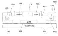
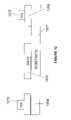
- FIG. 1a cross-sectional diagram of a top-gate bottom contact organic MIS transistor 100 is shown.
- Two conductor regions 101 and 102 for the transistor source and drainare deposited and patterned on insulating substrate 112 .
- the gap between conductive regions 101 and 102is known as the “channel”, and is designated as 103 in FIG. 1 .
- a semiconductor layer 104is deposited on the conductive regions 101 and 102 . This semiconductor layer must overlap the channel 103 , but may or may not exist in other areas of the transistor. In FIG. 1 , the semiconductor has not been removed.
- a thin film of dielectric material 106is deposited on top of semiconductor layer 104 and source 101 and drain 102 .
- the dielectric 106may or may not be deposited in other areas as well. However, the dielectric 106 may not exist in any areas where the source or drain is to connect to conductive traces on top of the dielectric.
- a conductive film 108is deposited and patterned on top of dielectric 106 to form the gate of a transistor, which must completely overlap the channel region 103 .
- This conductive layermay also be patterned in other areas, which serve as appropriate connections between transistors.
- This conductive layer 108must make contact to the source/drain layer 101 / 102 as specified by the associated circuit design. Referring to the example in FIG. 1 , source 101 makes contact to conductive layer 110 and drain 102 makes contact to conductive layer 111 .
- electrical connectionsare made between the source/drain conductive layer to the gate layer 108 where the metal on the source/drain layer 101 / 102 is not necessarily used as a source or drain of a transistor, but rather an interconnect.
- the holes 113 and 114 that electrically connect the gate conductive layer to the source-drain conductive layerare called “vias”.
- these holesmay be created by not depositing the dielectric in those areas by use of a stamp or a shadow mask.
- subtractive processessuch as photolithography followed by etching by chemical, physical, or reactive ion means have been used for defining vias.
- Patterningrequires precise alignments so that the vias are precisely aligned with the conductor above the dielectric and below the dielectric to make good electrical contact.
- non-uniformity in the dielectricwill result in unreliable isolation of the conductive layers above and below the dielectric, resulting in undesired electrical connections.
- one printed areamay scavenge material from the other leading to an uneven distribution of material compromising uniformity.
- a low-cost and efficient method of fabricationis disclosed that can produce self-aligned vias in dielectric polymer films that provides electrical connection between a top conductor and a bottom conductor.
- the processis achieved by printing conductive posts on the first patterned conductive layer, followed by the deposition of an unpatterned layer dielectric, followed by the deposition of a second patterned conductive layer.
- the viais formed during the flash annealing of the post after the dielectric is deposited, but before the second conductive layer is deposited.
- the post materialis annealed with a flash of light, resulting in a release of energy which removes the dielectric on the top of the post.
- the post materialis chosen so that a volatile reaction causes the dielectric to be removed during the anneal of the post material.
- the post materialis not cured or only partially cured before the dielectric deposition.
- these conductive postsare chosen to include materials which repel the dielectric material.
- the post materialmay be cured, partially cured, or not cured before the dielectric, the process chosen to maximize the repelling properties of the dielectric material to the post material.
- Nano-particle conductive inksMaterials particularly appropriate as a choice of post material are nano-particle conductive inks.
- the dielectric materialis typically annealed at the curing temperature of the nano-particle ink.
- the method of the present inventioncan be generally used for creating via holes in most polymer thin films.
- FIG. 1illustrates a cross-sectional view of an organic FET transistor including an insulating substrate, organic polymer film, dielectric layer, vias and conductive gate according to the prior art
- FIGS. 2-4 and 9 - 11are sequential process steps for forming vias in a printed organic FET circuit according to the present invention wherein:
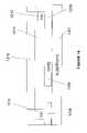
- FIG. 2illustrates a cross-sectional view of a process step wherein the source drain conductor is deposited on a substrate with defined source drain electrodes to give a partially processed substrate;
- FIG. 3illustrates a cross-sectional view of a next process step wherein the semiconductor is deposited and annealed
- FIG. 4illustrates a cross-sectional view of a next process wherein the nano-particle ink is deposited
- FIG. 5illustrates posts patterned via inkjet means
- FIG. 6illustrates posts patterned via flexography
- FIG. 7illustrates posts patterned via gravure
- FIG. 8illustrates posts patterned via screen printing
- FIG. 9illustrates a cross-sectional view of a next process step wherein the dielectric ink is deposited
- FIG. 10illustrates a cross-sectional view of a next process step wherein the sample is exposed to an optical flash
- FIG. 11illustrates a cross-sectional view of a next process step wherein the gate conductor is deposited
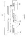
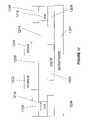
- FIGS. 12-18illustrates a cross sectional view of sequential steps to fabricate a bottom gate transistor according to the present invention, wherein:
- FIG. 12illustrates the initial steps to form a bottom gate transistor wherein the gate layer and the via post is deposited
- FIG. 13illustrates the next step in forming a bottom gate transistor wherein the dielectric is deposited
- FIG. 14illustrates a cross sectional view whereby the via openings are formed in a bottom gate device
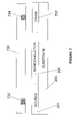
- FIG. 15illustrates a cross sectional view whereby the semiconductor is deposited in the formation of a top contact bottom gate device
- FIG. 16illustrates a cross sectional view whereby the via opening is formed through the semiconductor on a top contact bottom gate device
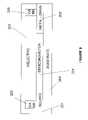
- FIG. 17illustrates a cross sectional view whereby the source and drain are deposited on a top gate bottom gate device
- FIG. 18illustrates a cross sectional view whereby the semiconductor and source/drain layers are deposited to form a bottom contact bottom gate device.
- the via formation according to the present inventionis described with respect to the fabrication of a top gate organic transistor in FIGS. 2-4 and 9 - 11 and with respect to the fabrication of a bottom gate organic transistor in FIGS. 12-18 .
- the source/drain conductorcan be of any material that conducts electricity, including metals, conducting polymers, or nano-particle ink.
- the preferred deposition meansdepends on the material, including sublimation and evaporation of a solid source, or deposition by means of a liquid. Patterning can be achieved through a shadow mask, by directly depositing the pattern of interest, or by means of a deposition followed by removal of unwanted materials.
- the substratemust be electrically insulating, consisting of either flexible or rigid material. Flexible substrate materials include PET, PEN, Kapton, mylar, and paper. Rigid materials include silicon with silicon dioxide, sapphire, or other insulating materials.
- semiconductor 204is deposited between the source and drain 201 , 202 and the substrate 203 .
- the semiconductormay also be applied in other areas of the circuit, but must at a minimum exist in the channel region between source 201 and drain 202 .
- the semiconductor materialincludes any material exhibiting semiconductor properties, including organic compounds such as polythiophene, pentacene and inorganic materials such as silicon.
- the semiconductoroverlaps the top of the source and the drain, partially or entirely.
- the semiconductoris not patterned at all, but rather deposited as a layer over the entirety of the circuit.
- conductive posts 205 and 206are deposited on the source 201 and the drain 202 .
- Posts 205 and 206are placed on the source and drain where an electrical connection is required by circuit design to subsequent conductive layers. It is not necessary that every source and drain require such a connection. Such connections can also be made on conductive traces which are not necessarily used as the source or drain of a transistor.
- the conductive posts 205 and 206can be made of any material, but is preferably chosen to interact appropriately with the subsequently deposited dielectric material.
- the post materialis chosen so that it will “flash anneal”, whereby significant energy is released during the anneal process. This post material may be partially cured at this step or not cured at all. The final anneal process is completed after the dielectric has been deposited.
- the postsare deposited by inkjet printer as illustrated in FIG. 5 .
- One or more drops of ink 530is ejected through nozzle 532 by physically compressing the chamber 534 through mechanisms including contracting a ferroelectric surface.
- the inkcan be expanded in the chamber 534 or the nozzle 532 by thermal means. Properties of the ink, such a viscosity and surface tension, are chosen to form an appropriate structure on the deposition surface.
- the postsare deposited by flexographic means as illustrated in FIG. 6 .
- a raised pattern of posts 632is formed on a flexographic plate 630 .
- the raised surfaces 632are covered with ink 634 , and are aligned and placed in contact with the areas where the posts are to be printed, thereby transferring the ink 634 onto the source and drain 201 and 202 .
- the print platecan be flat or can be placed on a roller wherein a continuous feed of substrate is rolled underneath the roller to form a roll-to-roll print flexographic platform.
- the postsare deposited by gravure means as illustrated in FIG. 7 .
- Cavitiesalso called cells 732 and 734 , are formed on gravure plate 730 .
- the plateis submerged in ink and is then scraped clean, thereby leaving ink in cells 732 and 734 .
- the plateis then placed in contact with the area on which the posts are printed, source 201 and drain 202 .
- the inkis then transferred to the surface of the source 201 and drain 202 .
- the gravure platecan be flat, or can be mounted on a roller wherein a continuous feed of substrate is rolled beneath the roller to form a roll-to-roll gravure print process.
- the postsare deposited by silk screen means as illustrated in FIG. 8 .
- the locations where posts are to be printedwill have openings in a wire or nylon meshed sheet 830 .
- the screenis placed in contact with the surface to be printed, such that the openings 832 and 834 are aligned with the prospective print locations, source 201 and drain 202 .
- the inkis then placed on the top surface of the screen, and pressed through the openings by means of a squeegee on the top surface of the screen plate 830 .
- the screencan also be mounted on a roller, utilizing rotorary screen printing. With rotorary screen printing, a continuous feed of substrate can be printed to form a roll-to-roll screen printing process.
- the post materialis chosen so that it will react in a volatile fashion during the anneal.
- the post materialmay be partially cured at this step or not cured at all. This is achieved by utilizing a thermally volatile polymer as the post material that tends to volatilize at temperatures higher than a given temperature T. This temperature is achieved during the final anneal process after the dielectric has been deposited.
- the post materialis chosen so that it will repel the dielectric material.
- the post materialmay be cured at this step, partially cured or not at all. The appropriate process is chosen to maximize the repelling properties of the dielectric to the post material.
- a different sacrificial polymer of a polarity opposite to that of the dielectricis deposited in the via locations over the post material.
- this polymercauses the dielectric to de-wet and self align the vias.
- the resulting vias in this casecan be filled in by the deposited gate metal after the sacrificial polymer is removed.
- the dielectric ink 207is deposited.
- the dielectricwill overlap semiconductor 204 , source 201 and drain 202 regions, as well as post 205 and 206 . This can be accomplished by depositing a patterned dielectric or by coating the entire surface with the dielectric without patterning. In one embodiment, the dielectric covers the top of the posts 205 and 206 .
- the height of the dielectricis lower than the height of the posts 205 and 206 , thereby leaving the top of the posts exposed.
- the dielectricis repelled by the post material, leaving the top of the posts without any dielectric material. This can be achieved if the dielectric solution is hydrophobic, the post material is hydrophilic, or vice versa. This difference in wetting properties causes the dielectric to move away or de-wet from the locations at which it contacts the nano-particle ink and thus allows self alignment of the vias.
- the surface of the dielectricis exposed to light which causes the post material to cure via “flash anneal”.
- the processreleases energy which causes remaining dielectric 208 and 209 on top of the post 205 and 206 to be removed, thereby exposing the top of the posts.
- this flash annealis made through the bottom of the substrate in cases where the flash radiation can pass through the substrate material.
- the post materialis annealed thermally or by rapid thermal anneal, whereby the dielectric material is removed from the top of the post through a volatile reaction.
- the post materialrepels the dielectric material, thereby leaving the top of the post without dielectric. If the post material was not completely annealed earlier, the anneal process can be completed at this stage.
- the anneal performed for the sake of the post materialalso serves to anneal the dielectric material.
- the gate conductor 210is deposited, patterned, and annealed to complete the circuit fabrication.
- conductive layer 210In order to form a gate of a transistor, conductive layer 210 must overlap the channel region between source 201 and drain 202 .
- Conductive layer 210may also be patterned to correspond to the gate of another transistor, or may be used as a conductive interconnect or to provide the conductive means on that layer for any purpose.
- the gate conductorincludes any conducting material, including metal, conducting nano-particles, or conducting polymer. Patterning is achieved either by depositing a solution or ink in the patterned fashion using print technology such as gravure, inkjet, flexography, or silk screening. Alternatively, the gate metal can be patterned using a shadow mask during deposition, or subsequently removing unwanted material via a photo resist process.
- the area 208 and 209 above posts 205 and 206have no dielectric or semiconductor over it since it has been removed by the methods described above. Therefore, where the conductive layer 210 makes contact to a post 205 or 206 , an electrical connection is made between the first source/drain conductive layer and the second gate layer conductor through the materials between them.
- the primary purpose of the source/drain conductive layeris to define the source/drain of a transistor and the primary purpose of the gate conductive layer is to define the gate layer, either layer can pattern metal for any other purpose such as the creation of a capacitor, resistor, inductor, or as an interconnect.
- a patterned conductive layer including gate conductor 1202 and conductive regions 1204 and 1206are formed on substrate 1201 .
- This patterncan be obtained by depositing a fluid conductor directly on substrate 1201 , by evaporating a conductive solid through a shadow mask, or by first covering the entire substrate with the conductive layer followed by selective removal.
- the conductive gate materialcan include any conductive substance including metal, conductive polymer, or nano-particle metal ink solution.
- the postsare then deposited on the surfaces 1204 and 1206 using any of the same methods described above, to form via 1210 and 1212 .
- the dielectric 1214is deposited over vias 1210 and 1212 .
- the dielectric 1214could cover the entire area, as shown in FIG. 13 .
- the dielectric 1214could be deposited in a pattern wherein at minimum all conductive regions on the gate layer are covered. The areas between conductive regions can also be covered, but can be left uncovered if so desired.
- the via metal openingsare now formed by flash light anneal, or thermal anneal by methods as described above, the energy release of which remove the dielectric above the via post.
- a semiconductor layer 1216is formed over the dielectric layer 1214 , as shown.
- the semiconductor layer 1216can be formed prior to forming the via openings. In either case, the semiconductor 1216 must overlap all areas that make up the gate of the transistor.
- the semiconductor 1216may or may not be placed in areas other than the gate conductor, including over the via regions.
- the semiconductor 1216may cover the entire surface area. As illustrated in FIG. 16 , methods described above to open vias 1210 and 1212 can be used to open the dielectric and semiconductor over the via.
- a “top contact bottom gate” structureis formed by depositing semiconductor 1216 before a conductive source/drain layer to form source 1222 , drain 1224 , and conductive regions 1220 and 1226 , as illustrated in FIG. 17 .
- Conductive regions 1220 and 1226represent conductive interconnect that is routed to other areas of the chip for appropriate electrical contact. At least a portion of source 1222 and drain 1224 must overlap the gate 1202 in order to form a transistor. The area between source 1222 and 1224 is the channel region of the transistor, which must be entirely overlapped by the gate.
- a “bottom contact top gate” structureis formed by depositing the semiconductor after the patterned gate layer is defined.
- the space between the source 1222 and the drain 1224establishes the channel region.
- the channel regionmust be completely overlapped by the gate 1202 .
- the semiconductor 1216at a minimum must cover the entire channel region.
- the semiconductormay cover the source 1222 and drain 1224 , and may cover any other areas.
- the semiconductor layer 1216can even be applied without patterning at all. In this case, the via opening techniques described above will break an opening through the dielectric and semiconductor sandwich.
Landscapes
- Engineering & Computer Science (AREA)
- Manufacturing & Machinery (AREA)
- Thin Film Transistor (AREA)
- Electrodes Of Semiconductors (AREA)
- Internal Circuitry In Semiconductor Integrated Circuit Devices (AREA)
- Electroluminescent Light Sources (AREA)
- Production Of Multi-Layered Print Wiring Board (AREA)
Abstract
Description
- The present invention relates to organic transistors used in printed circuits and, more particularly to a method of fabricating via holes in polymer dielectrics to connect one conductive layer with another.
- Organic field-effect transistors (oFETs) have been proposed for a number of applications including displays, electronic barcodes and sensors. Low cost processes, large-area circuits and the chemically active nature of organic materials are the chief driving forces to make oFETs important in various applications. Many of these objectives depend on a method of fabrication utilizing printing techniques such as flexography, gravure, silk screen and inkjet printing.
- Printed top gate and bottom gate structured transistors and circuits have been demonstrated in the past. Usually, such a system consists of printed semiconductor, dielectric and gate conductors on flexible substrates.
- Referring now to
FIG. 1 , a cross-sectional diagram of a top-gate bottom contactorganic MIS transistor 100 is shown. Twoconductor regions insulating substrate 112. The gap betweenconductive regions FIG. 1 . Asemiconductor layer 104 is deposited on theconductive regions channel 103, but may or may not exist in other areas of the transistor. InFIG. 1 , the semiconductor has not been removed. - A thin film of
dielectric material 106 is deposited on top ofsemiconductor layer 104 andsource 101 anddrain 102. The dielectric106 may or may not be deposited in other areas as well. However, the dielectric106 may not exist in any areas where the source or drain is to connect to conductive traces on top of the dielectric. - A
conductive film 108 is deposited and patterned on top of dielectric106 to form the gate of a transistor, which must completely overlap thechannel region 103. This conductive layer may also be patterned in other areas, which serve as appropriate connections between transistors. Thisconductive layer 108 must make contact to the source/drain layer 101/102 as specified by the associated circuit design. Referring to the example inFIG. 1 ,source 101 makes contact toconductive layer 110 anddrain 102 makes contact toconductive layer 111. Depending on circuit configuration, it is also possible that electrical connections are made between the source/drain conductive layer to thegate layer 108 where the metal on the source/drain layer 101/102 is not necessarily used as a source or drain of a transistor, but rather an interconnect. - The
holes - Patterning requires precise alignments so that the vias are precisely aligned with the conductor above the dielectric and below the dielectric to make good electrical contact. In addition, non-uniformity in the dielectric will result in unreliable isolation of the conductive layers above and below the dielectric, resulting in undesired electrical connections.
- In some cases, when features having two different shapes are printed close to each other, one printed area may scavenge material from the other leading to an uneven distribution of material compromising uniformity. These undesirable phenomena are exacerbated with the increasing complexity of the circuits that require printing of a larger number of smaller features.
- What is desired, therefore, is a practical scalable process utilizing low cost printing techniques that can circumvent the described limitations of the prior art to provide electrical contact between the gate metal layer and the source/drain metal layer in a printed organic field-effect transistor circuit.
- According to the present invention, a low-cost and efficient method of fabrication is disclosed that can produce self-aligned vias in dielectric polymer films that provides electrical connection between a top conductor and a bottom conductor.
- The process is achieved by printing conductive posts on the first patterned conductive layer, followed by the deposition of an unpatterned layer dielectric, followed by the deposition of a second patterned conductive layer.
- In one embodiment, the via is formed during the flash annealing of the post after the dielectric is deposited, but before the second conductive layer is deposited. In this process, the post material is annealed with a flash of light, resulting in a release of energy which removes the dielectric on the top of the post.
- In another embodiment, the post material is chosen so that a volatile reaction causes the dielectric to be removed during the anneal of the post material. In this case, the post material is not cured or only partially cured before the dielectric deposition.
- In yet another embodiment, these conductive posts are chosen to include materials which repel the dielectric material. In this embodiment, the post material may be cured, partially cured, or not cured before the dielectric, the process chosen to maximize the repelling properties of the dielectric material to the post material.
- Materials particularly appropriate as a choice of post material are nano-particle conductive inks. The dielectric material is typically annealed at the curing temperature of the nano-particle ink.
- The method of the present invention can be generally used for creating via holes in most polymer thin films.
- The present invention is illustrated by way of example and not by limitation in the accompanying figures in which like reference numerals indicate similar elements and in which:
FIG. 1 illustrates a cross-sectional view of an organic FET transistor including an insulating substrate, organic polymer film, dielectric layer, vias and conductive gate according to the prior art;FIGS. 2-4 and9-11 are sequential process steps for forming vias in a printed organic FET circuit according to the present invention wherein:FIG. 2 illustrates a cross-sectional view of a process step wherein the source drain conductor is deposited on a substrate with defined source drain electrodes to give a partially processed substrate;FIG. 3 illustrates a cross-sectional view of a next process step wherein the semiconductor is deposited and annealed;FIG. 4 illustrates a cross-sectional view of a next process wherein the nano-particle ink is deposited;FIG. 5 illustrates posts patterned via inkjet means;FIG. 6 illustrates posts patterned via flexography;FIG. 7 illustrates posts patterned via gravure;FIG. 8 illustrates posts patterned via screen printing;FIG. 9 illustrates a cross-sectional view of a next process step wherein the dielectric ink is deposited;FIG. 10 illustrates a cross-sectional view of a next process step wherein the sample is exposed to an optical flash;FIG. 11 illustrates a cross-sectional view of a next process step wherein the gate conductor is deposited;FIGS. 12-18 illustrates a cross sectional view of sequential steps to fabricate a bottom gate transistor according to the present invention, wherein:FIG. 12 illustrates the initial steps to form a bottom gate transistor wherein the gate layer and the via post is deposited;FIG. 13 illustrates the next step in forming a bottom gate transistor wherein the dielectric is deposited;FIG. 14 illustrates a cross sectional view whereby the via openings are formed in a bottom gate device;FIG. 15 illustrates a cross sectional view whereby the semiconductor is deposited in the formation of a top contact bottom gate device;FIG. 16 illustrates a cross sectional view whereby the via opening is formed through the semiconductor on a top contact bottom gate device;FIG. 17 illustrates a cross sectional view whereby the source and drain are deposited on a top gate bottom gate device; andFIG. 18 illustrates a cross sectional view whereby the semiconductor and source/drain layers are deposited to form a bottom contact bottom gate device.- The via formation according to the present invention is described with respect to the fabrication of a top gate organic transistor in
FIGS. 2-4 and9-11 and with respect to the fabrication of a bottom gate organic transistor inFIGS. 12-18 . - Referring now to
FIG. 2 , a source and drain conductor,201 and202, respectively, is patterned on insulatingsubstrate 203. The source/drain conductor can be of any material that conducts electricity, including metals, conducting polymers, or nano-particle ink. The preferred deposition means depends on the material, including sublimation and evaporation of a solid source, or deposition by means of a liquid. Patterning can be achieved through a shadow mask, by directly depositing the pattern of interest, or by means of a deposition followed by removal of unwanted materials. The substrate must be electrically insulating, consisting of either flexible or rigid material. Flexible substrate materials include PET, PEN, Kapton, mylar, and paper. Rigid materials include silicon with silicon dioxide, sapphire, or other insulating materials. - Referring now to
FIG. 3 ,semiconductor 204 is deposited between the source and drain201,202 and thesubstrate 203. The semiconductor may also be applied in other areas of the circuit, but must at a minimum exist in the channel region betweensource 201 and drain202. The semiconductor material includes any material exhibiting semiconductor properties, including organic compounds such as polythiophene, pentacene and inorganic materials such as silicon. In another embodiment, the semiconductor overlaps the top of the source and the drain, partially or entirely. In yet another embodiment, the semiconductor is not patterned at all, but rather deposited as a layer over the entirety of the circuit. - Referring now to
FIG. 4 ,conductive posts source 201 and thedrain 202.Posts - The
conductive posts - In one embodiment, the posts are deposited by inkjet printer as illustrated in
FIG. 5 . One or more drops ofink 530 is ejected throughnozzle 532 by physically compressing thechamber 534 through mechanisms including contracting a ferroelectric surface. Alternatively, the ink can be expanded in thechamber 534 or thenozzle 532 by thermal means. Properties of the ink, such a viscosity and surface tension, are chosen to form an appropriate structure on the deposition surface. - In another embodiment, the posts are deposited by flexographic means as illustrated in
FIG. 6 . A raised pattern ofposts 632 is formed on aflexographic plate 630. The raised surfaces632 are covered withink 634, and are aligned and placed in contact with the areas where the posts are to be printed, thereby transferring theink 634 onto the source and drain201 and202. The print plate can be flat or can be placed on a roller wherein a continuous feed of substrate is rolled underneath the roller to form a roll-to-roll print flexographic platform. - In another embodiment, the posts are deposited by gravure means as illustrated in
FIG. 7 . Cavities, also calledcells gravure plate 730. The plate is submerged in ink and is then scraped clean, thereby leaving ink incells source 201 and drain202. The ink is then transferred to the surface of thesource 201 and drain202. The gravure plate can be flat, or can be mounted on a roller wherein a continuous feed of substrate is rolled beneath the roller to form a roll-to-roll gravure print process. - In yet another embodiment, the posts are deposited by silk screen means as illustrated in
FIG. 8 . The locations where posts are to be printed will have openings in a wire or nylon meshedsheet 830. The screen is placed in contact with the surface to be printed, such that theopenings source 201 and drain202. The ink is then placed on the top surface of the screen, and pressed through the openings by means of a squeegee on the top surface of thescreen plate 830. The screen can also be mounted on a roller, utilizing rotorary screen printing. With rotorary screen printing, a continuous feed of substrate can be printed to form a roll-to-roll screen printing process. - In another embodiment, the post material is chosen so that it will react in a volatile fashion during the anneal. The post material may be partially cured at this step or not cured at all. This is achieved by utilizing a thermally volatile polymer as the post material that tends to volatilize at temperatures higher than a given temperature T. This temperature is achieved during the final anneal process after the dielectric has been deposited.
- In yet another embodiment, the post material is chosen so that it will repel the dielectric material. In this case, the post material may be cured at this step, partially cured or not at all. The appropriate process is chosen to maximize the repelling properties of the dielectric to the post material.
- In yet another embodiment, a different sacrificial polymer of a polarity opposite to that of the dielectric is deposited in the via locations over the post material. In that scenario, this polymer causes the dielectric to de-wet and self align the vias. The resulting vias in this case can be filled in by the deposited gate metal after the sacrificial polymer is removed.
- Referring now to
FIG. 9 , thedielectric ink 207 is deposited. The dielectric will overlapsemiconductor 204,source 201 and drain202 regions, as well aspost posts - In another embodiment, the height of the dielectric is lower than the height of the
posts - Referring now to
FIG. 10 , the surface of the dielectric is exposed to light which causes the post material to cure via “flash anneal”. In this embodiment, the process releases energy which causes remainingdielectric post - In another embodiment, the post material is annealed thermally or by rapid thermal anneal, whereby the dielectric material is removed from the top of the post through a volatile reaction.
- In yet another embodiment, the post material repels the dielectric material, thereby leaving the top of the post without dielectric. If the post material was not completely annealed earlier, the anneal process can be completed at this stage.
- In yet another embodiment, the anneal performed for the sake of the post material also serves to anneal the dielectric material.
- Referring now to
FIG. 11 , thegate conductor 210 is deposited, patterned, and annealed to complete the circuit fabrication. In order to form a gate of a transistor,conductive layer 210 must overlap the channel region betweensource 201 and drain202.Conductive layer 210 may also be patterned to correspond to the gate of another transistor, or may be used as a conductive interconnect or to provide the conductive means on that layer for any purpose. - The gate conductor includes any conducting material, including metal, conducting nano-particles, or conducting polymer. Patterning is achieved either by depositing a solution or ink in the patterned fashion using print technology such as gravure, inkjet, flexography, or silk screening. Alternatively, the gate metal can be patterned using a shadow mask during deposition, or subsequently removing unwanted material via a photo resist process.
- The
area above posts conductive layer 210 makes contact to apost - The same via formation method according to the present invention can also be used in a bottom gate construction as illustrated in
FIG. 12 . A patterned conductive layer includinggate conductor 1202 andconductive regions substrate 1201. This pattern can be obtained by depositing a fluid conductor directly onsubstrate 1201, by evaporating a conductive solid through a shadow mask, or by first covering the entire substrate with the conductive layer followed by selective removal. The conductive gate material can include any conductive substance including metal, conductive polymer, or nano-particle metal ink solution. - The posts are then deposited on the
surfaces - Referring now to
FIG. 13 , the dielectric1214 is deposited overvias FIG. 13 . Alternatively, the dielectric1214 could be deposited in a pattern wherein at minimum all conductive regions on the gate layer are covered. The areas between conductive regions can also be covered, but can be left uncovered if so desired. - As illustrated in
FIG. 14 , the via metal openings are now formed by flash light anneal, or thermal anneal by methods as described above, the energy release of which remove the dielectric above the via post. - In
FIG. 15 , asemiconductor layer 1216 is formed over thedielectric layer 1214, as shown. In another embodiment, thesemiconductor layer 1216 can be formed prior to forming the via openings. In either case, thesemiconductor 1216 must overlap all areas that make up the gate of the transistor. - The
semiconductor 1216 may or may not be placed in areas other than the gate conductor, including over the via regions. Thesemiconductor 1216 may cover the entire surface area. As illustrated inFIG. 16 , methods described above to openvias - In one embodiment, a “top contact bottom gate” structure is formed by depositing
semiconductor 1216 before a conductive source/drain layer to formsource 1222,drain 1224, andconductive regions FIG. 17 .Conductive regions source 1222 and drain1224 must overlap thegate 1202 in order to form a transistor. The area betweensource - In another embodiment illustrated in
FIG. 18 , a “bottom contact top gate” structure is formed by depositing the semiconductor after the patterned gate layer is defined. In this structure, the space between thesource 1222 and thedrain 1224 establishes the channel region. The channel region must be completely overlapped by thegate 1202. Thesemiconductor 1216, at a minimum must cover the entire channel region. Alternatively, the semiconductor may cover thesource 1222 anddrain 1224, and may cover any other areas. Thesemiconductor layer 1216 can even be applied without patterning at all. In this case, the via opening techniques described above will break an opening through the dielectric and semiconductor sandwich. - While the invention has been described in detail in the foregoing description and illustrative embodiment, it will be appreciated by those skilled in the art that many variations may be made without departing from the spirit and scope of the invention. Thus, it may be understood, for example, that the structures above could include a variety of different nano-particles, polymers and various print methodologies can be used to achieve this result. The process may also include surface treatments at various steps as well as modified transistor structures, including structures such as top-gate top-electrode, top-gate bottom-electrode, bottom gate top-electrode, bottom gate bottom electrode and vertical FETs.
Claims (14)
Priority Applications (7)
| Application Number | Priority Date | Filing Date | Title |
|---|---|---|---|
| US11/764,326US7858513B2 (en) | 2007-06-18 | 2007-06-18 | Fabrication of self-aligned via holes in polymer thin films |
| JP2008117116AJP2008311630A (en) | 2007-06-18 | 2008-04-28 | Formation of self-aligned via holes in polymer thin films |
| KR1020080042132AKR100956253B1 (en) | 2007-06-18 | 2008-05-07 | Assembly of Self Aligned Via Holes in Polymer Thin Films |
| EP08155964AEP2006930A3 (en) | 2007-06-18 | 2008-05-09 | Fabrication of self-aligned via holes in polymer thin films |
| SG200803774-9ASG148921A1 (en) | 2007-06-18 | 2008-05-16 | Fabrication of self-aligned via holes in polymer thin films |
| CN2008101000323ACN101330130B (en) | 2007-06-18 | 2008-06-03 | Fabrication of self-aligned via holes in polymer thin films |
| JP2012089162AJP5638565B2 (en) | 2007-06-18 | 2012-04-10 | Formation of self-aligned via holes in polymer thin films |
Applications Claiming Priority (1)
| Application Number | Priority Date | Filing Date | Title |
|---|---|---|---|
| US11/764,326US7858513B2 (en) | 2007-06-18 | 2007-06-18 | Fabrication of self-aligned via holes in polymer thin films |
Publications (2)
| Publication Number | Publication Date |
|---|---|
| US20080311698A1true US20080311698A1 (en) | 2008-12-18 |
| US7858513B2 US7858513B2 (en) | 2010-12-28 |
Family
ID=39791013
Family Applications (1)
| Application Number | Title | Priority Date | Filing Date |
|---|---|---|---|
| US11/764,326Expired - Fee RelatedUS7858513B2 (en) | 2007-06-18 | 2007-06-18 | Fabrication of self-aligned via holes in polymer thin films |
Country Status (6)
| Country | Link |
|---|---|
| US (1) | US7858513B2 (en) |
| EP (1) | EP2006930A3 (en) |
| JP (2) | JP2008311630A (en) |
| KR (1) | KR100956253B1 (en) |
| CN (1) | CN101330130B (en) |
| SG (1) | SG148921A1 (en) |
Cited By (4)
| Publication number | Priority date | Publication date | Assignee | Title |
|---|---|---|---|---|
| WO2009085599A1 (en)* | 2007-12-26 | 2009-07-09 | Weyerhaeuser Company | Organic semiconductor device and method of manufacturing same |
| US20100009497A1 (en)* | 2008-07-11 | 2010-01-14 | Weyerhaeuser Company | Performance improvements of ofets through use of field oxide to control ink flow |
| US20110024179A1 (en)* | 2009-07-30 | 2011-02-03 | Sony Corporation | Method for producing circuit board and circuit board |
| US20110095342A1 (en)* | 2009-10-23 | 2011-04-28 | Palo Alto Research Center Incorporated | Printed Material Constrained By Well Structures And Devices Including Same |
Families Citing this family (6)
| Publication number | Priority date | Publication date | Assignee | Title |
|---|---|---|---|---|
| US9059257B2 (en) | 2013-09-30 | 2015-06-16 | International Business Machines Corporation | Self-aligned vias formed using sacrificial metal caps |
| US10492305B2 (en) | 2015-06-30 | 2019-11-26 | 3M Innovative Properties Company | Patterned overcoat layer |
| US10361128B2 (en) | 2017-01-11 | 2019-07-23 | International Business Machines Corporation | 3D vertical FET with top and bottom gate contacts |
| US20200185322A1 (en)* | 2018-12-07 | 2020-06-11 | Texas Instruments Incorporated | Semiconductor device connections with sintered nanoparticles |
| KR20210011715A (en) | 2019-07-23 | 2021-02-02 | 박상태 | An electric flyswatter type and rotation length is adjustable for removable |
| US11289375B2 (en) | 2020-03-23 | 2022-03-29 | International Business Machines Corporation | Fully aligned interconnects with selective area deposition |
Citations (18)
| Publication number | Priority date | Publication date | Assignee | Title |
|---|---|---|---|---|
| US5130274A (en)* | 1991-04-05 | 1992-07-14 | International Business Machines Corporation | Copper alloy metallurgies for VLSI interconnection structures |
| US6015751A (en)* | 1998-04-06 | 2000-01-18 | Taiwan Semiconductor Manufacturing Company | Self-aligned connection to underlayer metal lines through unlanded via holes |
| US6091152A (en)* | 1994-04-15 | 2000-07-18 | Sharp Kabushiki Kaisha | Semiconductor device and method for fabricating the same |
| US6159839A (en)* | 1999-02-11 | 2000-12-12 | Vanguard International Semiconductor Corporation | Method for fabricating borderless and self-aligned polysilicon and metal contact landing plugs for multilevel interconnections |
| US6187668B1 (en)* | 1999-07-06 | 2001-02-13 | United Microelectronics Corp. | Method of forming self-aligned unlanded via holes |
| US20020047207A1 (en)* | 1997-08-21 | 2002-04-25 | Matsushita Electronics Corporation | Semiconductor device and method for fabricating the same |
| US20020127844A1 (en)* | 2000-08-31 | 2002-09-12 | International Business Machines Corporation | Multilevel interconnect structure containing air gaps and method for making |
| US20020149110A1 (en)* | 1997-06-13 | 2002-10-17 | Ahn Kie Y. | Multilevel interconnect structure with low-k dielectric and method of fabricating the structure |
| US6635566B1 (en)* | 2000-06-15 | 2003-10-21 | Cypress Semiconductor Corporation | Method of making metallization and contact structures in an integrated circuit |
| US6723631B2 (en)* | 2000-09-29 | 2004-04-20 | Renesas Technology Corporation | Fabrication method of semiconductor integrated circuit device |
| US20040099951A1 (en)* | 2002-11-21 | 2004-05-27 | Hyun-Mog Park | Air gap interconnect structure and method |
| US20040099952A1 (en)* | 2002-11-21 | 2004-05-27 | Goodner Michael D. | Formation of interconnect structures by removing sacrificial material with supercritical carbon dioxide |
| US6943067B2 (en)* | 2002-01-08 | 2005-09-13 | Advanced Micro Devices, Inc. | Three-dimensional integrated semiconductor devices |
| US6987031B2 (en)* | 2002-08-27 | 2006-01-17 | Micron Technology, Inc. | Multiple chip semiconductor package and method of fabricating same |
| US20060094178A1 (en)* | 2004-10-21 | 2006-05-04 | Nanya Technology Corporation | Method of fabricating MOS transistor by millisecond anneal |
| US7084479B2 (en)* | 2003-12-08 | 2006-08-01 | International Business Machines Corporation | Line level air gaps |
| US20070020798A1 (en)* | 2005-07-22 | 2007-01-25 | Xerox Corporation | Methods to minimize contact resistance |
| US7250365B2 (en)* | 2001-04-17 | 2007-07-31 | Renesas Technology Corp. | Fabrication method of semiconductor integrated circuit device |
Family Cites Families (22)
| Publication number | Priority date | Publication date | Assignee | Title |
|---|---|---|---|---|
| US5948533A (en)* | 1990-02-09 | 1999-09-07 | Ormet Corporation | Vertically interconnected electronic assemblies and compositions useful therefor |
| US5774340A (en)* | 1996-08-28 | 1998-06-30 | International Business Machines Corporation | Planar redistribution structure and printed wiring device |
| ATE434259T1 (en)* | 1997-10-14 | 2009-07-15 | Patterning Technologies Ltd | METHOD OF MAKING AN ELECTRICAL CAPACITOR |
| JP3439144B2 (en)* | 1998-12-22 | 2003-08-25 | 三洋電機株式会社 | Semiconductor device and manufacturing method thereof |
| CN100379048C (en)* | 1999-12-21 | 2008-04-02 | 造型逻辑有限公司 | form interconnection |
| JP2001267417A (en)* | 2000-03-23 | 2001-09-28 | Sanyo Electric Co Ltd | Manufacturing method of semiconductor device |
| JP2002299442A (en)* | 2001-03-30 | 2002-10-11 | Seiko Epson Corp | Method for manufacturing semiconductor device |
| CN1237855C (en) | 2002-06-24 | 2006-01-18 | 威盛电子股份有限公司 | Method for making circuit substrate via hole and circuit by printing method |
| JP2005032769A (en) | 2003-07-07 | 2005-02-03 | Seiko Epson Corp | Multilayer wiring formation method, wiring board manufacturing method, device manufacturing method |
| JP4619060B2 (en)* | 2003-08-15 | 2011-01-26 | 株式会社半導体エネルギー研究所 | Method for manufacturing semiconductor device |
| JP2005079288A (en)* | 2003-08-29 | 2005-03-24 | Seiko Epson Corp | Method for forming multilayer wiring and electronic device |
| JP2005142277A (en)* | 2003-11-05 | 2005-06-02 | Seiko Epson Corp | Pattern forming method, electro-optical device manufacturing method, device manufacturing method, electronic apparatus |
| JP4684625B2 (en)* | 2003-11-14 | 2011-05-18 | 株式会社半導体エネルギー研究所 | Method for manufacturing semiconductor device |
| US20050170643A1 (en)* | 2004-01-29 | 2005-08-04 | Semiconductor Energy Laboratory Co., Ltd. | Forming method of contact hole, and manufacturing method of semiconductor device, liquid crystal display device and EL display device |
| JP4281584B2 (en)* | 2004-03-04 | 2009-06-17 | セイコーエプソン株式会社 | Manufacturing method of semiconductor device |
| CN1743928A (en)* | 2004-08-30 | 2006-03-08 | 财团法人工业技术研究院 | Fabrication method and structure of top-emission organic light-emitting diode pixel |
| GB2418062A (en) | 2004-09-03 | 2006-03-15 | Seiko Epson Corp | An organic Field-Effect Transistor with a charge transfer injection layer |
| KR20070014579A (en)* | 2005-07-29 | 2007-02-01 | 삼성전자주식회사 | Organic thin film transistor array panel and manufacturing method thereof |
| KR101219046B1 (en)* | 2005-11-17 | 2013-01-08 | 삼성디스플레이 주식회사 | Display device and manufacturing method thereof |
| KR100659112B1 (en) | 2005-11-22 | 2006-12-19 | 삼성에스디아이 주식회사 | Organic thin film transistor and manufacturing method thereof, flat display device having same |
| KR100766318B1 (en)* | 2005-11-29 | 2007-10-11 | 엘지.필립스 엘시디 주식회사 | Thin film transistor using organic semiconductor material, array substrate for liquid crystal display device having same and manufacturing method thereof |
| KR100730183B1 (en) | 2005-12-12 | 2007-06-19 | 삼성에스디아이 주식회사 | Organic thin film transistor and manufacturing method thereof, flat display device having same |
- 2007
- 2007-06-18USUS11/764,326patent/US7858513B2/ennot_activeExpired - Fee Related
- 2008
- 2008-04-28JPJP2008117116Apatent/JP2008311630A/enactivePending
- 2008-05-07KRKR1020080042132Apatent/KR100956253B1/ennot_activeExpired - Fee Related
- 2008-05-09EPEP08155964Apatent/EP2006930A3/ennot_activeWithdrawn
- 2008-05-16SGSG200803774-9Apatent/SG148921A1/enunknown
- 2008-06-03CNCN2008101000323Apatent/CN101330130B/ennot_activeExpired - Fee Related
- 2012
- 2012-04-10JPJP2012089162Apatent/JP5638565B2/ennot_activeExpired - Fee Related
Patent Citations (18)
| Publication number | Priority date | Publication date | Assignee | Title |
|---|---|---|---|---|
| US5130274A (en)* | 1991-04-05 | 1992-07-14 | International Business Machines Corporation | Copper alloy metallurgies for VLSI interconnection structures |
| US6091152A (en)* | 1994-04-15 | 2000-07-18 | Sharp Kabushiki Kaisha | Semiconductor device and method for fabricating the same |
| US20020149110A1 (en)* | 1997-06-13 | 2002-10-17 | Ahn Kie Y. | Multilevel interconnect structure with low-k dielectric and method of fabricating the structure |
| US20020047207A1 (en)* | 1997-08-21 | 2002-04-25 | Matsushita Electronics Corporation | Semiconductor device and method for fabricating the same |
| US6015751A (en)* | 1998-04-06 | 2000-01-18 | Taiwan Semiconductor Manufacturing Company | Self-aligned connection to underlayer metal lines through unlanded via holes |
| US6159839A (en)* | 1999-02-11 | 2000-12-12 | Vanguard International Semiconductor Corporation | Method for fabricating borderless and self-aligned polysilicon and metal contact landing plugs for multilevel interconnections |
| US6187668B1 (en)* | 1999-07-06 | 2001-02-13 | United Microelectronics Corp. | Method of forming self-aligned unlanded via holes |
| US6635566B1 (en)* | 2000-06-15 | 2003-10-21 | Cypress Semiconductor Corporation | Method of making metallization and contact structures in an integrated circuit |
| US20020127844A1 (en)* | 2000-08-31 | 2002-09-12 | International Business Machines Corporation | Multilevel interconnect structure containing air gaps and method for making |
| US6723631B2 (en)* | 2000-09-29 | 2004-04-20 | Renesas Technology Corporation | Fabrication method of semiconductor integrated circuit device |
| US7250365B2 (en)* | 2001-04-17 | 2007-07-31 | Renesas Technology Corp. | Fabrication method of semiconductor integrated circuit device |
| US6943067B2 (en)* | 2002-01-08 | 2005-09-13 | Advanced Micro Devices, Inc. | Three-dimensional integrated semiconductor devices |
| US6987031B2 (en)* | 2002-08-27 | 2006-01-17 | Micron Technology, Inc. | Multiple chip semiconductor package and method of fabricating same |
| US20040099951A1 (en)* | 2002-11-21 | 2004-05-27 | Hyun-Mog Park | Air gap interconnect structure and method |
| US20040099952A1 (en)* | 2002-11-21 | 2004-05-27 | Goodner Michael D. | Formation of interconnect structures by removing sacrificial material with supercritical carbon dioxide |
| US7084479B2 (en)* | 2003-12-08 | 2006-08-01 | International Business Machines Corporation | Line level air gaps |
| US20060094178A1 (en)* | 2004-10-21 | 2006-05-04 | Nanya Technology Corporation | Method of fabricating MOS transistor by millisecond anneal |
| US20070020798A1 (en)* | 2005-07-22 | 2007-01-25 | Xerox Corporation | Methods to minimize contact resistance |
Cited By (11)
| Publication number | Priority date | Publication date | Assignee | Title |
|---|---|---|---|---|
| WO2009085599A1 (en)* | 2007-12-26 | 2009-07-09 | Weyerhaeuser Company | Organic semiconductor device and method of manufacturing same |
| US20090239333A1 (en)* | 2007-12-26 | 2009-09-24 | Weyerhaeuser Co. | Organic semiconductor device and method of manufacturing the same |
| US7888169B2 (en)* | 2007-12-26 | 2011-02-15 | Organicid, Inc. | Organic semiconductor device and method of manufacturing the same |
| US20100009497A1 (en)* | 2008-07-11 | 2010-01-14 | Weyerhaeuser Company | Performance improvements of ofets through use of field oxide to control ink flow |
| US7718466B2 (en)* | 2008-07-11 | 2010-05-18 | Organicid, Inc. | Performance improvements of OFETs through use of field oxide to control ink flow |
| US20110024179A1 (en)* | 2009-07-30 | 2011-02-03 | Sony Corporation | Method for producing circuit board and circuit board |
| US20110095342A1 (en)* | 2009-10-23 | 2011-04-28 | Palo Alto Research Center Incorporated | Printed Material Constrained By Well Structures And Devices Including Same |
| US8211782B2 (en)* | 2009-10-23 | 2012-07-03 | Palo Alto Research Center Incorporated | Printed material constrained by well structures |
| US8624304B2 (en) | 2009-10-23 | 2014-01-07 | Palo Alto Research Center Incorporated | Printed material constrained by well structures and devices including same |
| US9029245B2 (en) | 2009-10-23 | 2015-05-12 | Palo Alto Research Center Incorporated | Printed material constrained by well structures and devices including same |
| US9202683B2 (en) | 2009-10-23 | 2015-12-01 | Palo Alto Research Center Incorporated | Printed material constrained by well structures and devices including same |
Also Published As
| Publication number | Publication date |
|---|---|
| JP2012156543A (en) | 2012-08-16 |
| JP5638565B2 (en) | 2014-12-10 |
| EP2006930A3 (en) | 2011-03-23 |
| KR100956253B1 (en) | 2010-05-06 |
| US7858513B2 (en) | 2010-12-28 |
| JP2008311630A (en) | 2008-12-25 |
| EP2006930A2 (en) | 2008-12-24 |
| SG148921A1 (en) | 2009-01-29 |
| CN101330130B (en) | 2011-02-02 |
| CN101330130A (en) | 2008-12-24 |
| KR20080111386A (en) | 2008-12-23 |
Similar Documents
| Publication | Publication Date | Title |
|---|---|---|
| US7858513B2 (en) | Fabrication of self-aligned via holes in polymer thin films | |
| JP4994727B2 (en) | Organic transistor active substrate, manufacturing method thereof, and electrophoretic display using the organic transistor active substrate | |
| US6794676B2 (en) | Fabrication of organic light emitting diode using selective printing of conducting polymer layers | |
| US8372731B2 (en) | Device fabrication by ink-jet printing materials into bank structures, and embossing tool | |
| CN102334392B (en) | Method for manufacturing electronic component and electronic component manufactured by the method | |
| US7582509B2 (en) | Micro-embossing fabrication of electronic devices | |
| KR20100016643A (en) | Method for forming a pattern on a substrate and electronic device formed thereby | |
| JP2010028005A (en) | Semiconductor composite membrane, method of manufacturing same, thin film transistor, method of manufacturing thin film transistor, and electronic device | |
| JP2006073993A (en) | Organic thin film transistor manufacturing method, liquid crystal display device manufacturing method, and organic thin film transistor | |
| US8048725B2 (en) | Method of forming pattern and method of producing electronic element | |
| JP4760844B2 (en) | Electronic component manufacturing method and electronic component manufactured by the method | |
| KR20060063903A (en) | Stacking method of organic semiconductor | |
| KR100770729B1 (en) | Method of manufacturing semiconductor device and method of manufacturing electronic apparatus | |
| US7390752B2 (en) | Self-aligning patterning method | |
| JP5332145B2 (en) | Multilayer structure, electronic device, electronic device array, and display device | |
| US7632705B2 (en) | Method of high precision printing for manufacturing organic thin film transistor | |
| JP6241573B2 (en) | Manufacturing method of electronic device | |
| US8001491B2 (en) | Organic thin film transistor and method of fabricating the same | |
| US20060240668A1 (en) | Semiconductor device with metallic electrodes and a method for use in forming such a device | |
| JP2007073856A (en) | Formation method of conductive pattern, manufacturing method of semiconductor device, and manufacturing method of organic electroluminescent element | |
| JP2005142277A (en) | Pattern forming method, electro-optical device manufacturing method, device manufacturing method, electronic apparatus | |
| KR20090008694A (en) | Pattern Formation Method | |
| JP2006186293A (en) | Thin film transistor manufacturing method | |
| JP2007220713A (en) | Thin film transistor | |
| JP6620556B2 (en) | Functional material lamination method and functional material laminate |
Legal Events
| Date | Code | Title | Description |
|---|---|---|---|
| AS | Assignment | Owner name:WEYERHAEUSER COMPANY, WASHINGTON Free format text:ASSIGNMENT OF ASSIGNORS INTEREST;ASSIGNORS:MOHAPATRA, SIDDARTH;DIMMLER, KLAUS;JENKINS, PATRICK H.;REEL/FRAME:019475/0456;SIGNING DATES FROM 20070608 TO 20070614 Owner name:WEYERHAEUSER COMPANY, WASHINGTON Free format text:ASSIGNMENT OF ASSIGNORS INTEREST;ASSIGNORS:MOHAPATRA, SIDDARTH;DIMMLER, KLAUS;JENKINS, PATRICK H.;SIGNING DATES FROM 20070608 TO 20070614;REEL/FRAME:019475/0456 | |
| AS | Assignment | Owner name:WEYERHAEUSER COMPANY, WASHINGTON Free format text:CORRECTIVE ASSIGNMENT TO CORRECT THE FIRST INVENTOR'S NAME FROM SIDDARTH MOHAPATRA PREVIOUSLY RECORDED ON REEL 019475 FRAME 0456;ASSIGNORS:MOHAPATRA, SIDDHARTH;DIMMLER, KLAUS;JENKINS, PATRICK H;REEL/FRAME:020905/0582;SIGNING DATES FROM 20070608 TO 20070614 Owner name:WEYERHAEUSER COMPANY, WASHINGTON Free format text:CORRECTIVE ASSIGNMENT TO CORRECT THE FIRST INVENTOR'S NAME FROM SIDDARTH MOHAPATRA PREVIOUSLY RECORDED ON REEL 019475 FRAME 0456. ASSIGNOR(S) HEREBY CONFIRMS THE FIRST INVENTOR'S NAME TO SIDDHARTH MOHAPATRA;ASSIGNORS:MOHAPATRA, SIDDHARTH;DIMMLER, KLAUS;JENKINS, PATRICK H;SIGNING DATES FROM 20070608 TO 20070614;REEL/FRAME:020905/0582 | |
| AS | Assignment | Owner name:ORGANICID, INC., COLORADO Free format text:ASSIGNMENT OF ASSIGNORS INTEREST;ASSIGNOR:WEYERHAEUSER COMPANY;REEL/FRAME:025369/0292 Effective date:20101115 | |
| STCF | Information on status: patent grant | Free format text:PATENTED CASE | |
| AS | Assignment | Owner name:TAP DEVELOPMENT LIMITED LIABILITY COMPANY, DELAWAR Free format text:ASSIGNMENT OF ASSIGNORS INTEREST;ASSIGNOR:ORGANICID, INC.;REEL/FRAME:027509/0920 Effective date:20111018 | |
| FPAY | Fee payment | Year of fee payment:4 | |
| AS | Assignment | Owner name:GULA CONSULTING LIMITED LIABILITY COMPANY, DELAWAR Free format text:MERGER;ASSIGNOR:TAP DEVELOPMENT LIMITED LIABILITY COMPANY;REEL/FRAME:037329/0414 Effective date:20150826 | |
| MAFP | Maintenance fee payment | Free format text:PAYMENT OF MAINTENANCE FEE, 8TH YEAR, LARGE ENTITY (ORIGINAL EVENT CODE: M1552) Year of fee payment:8 | |
| FEPP | Fee payment procedure | Free format text:MAINTENANCE FEE REMINDER MAILED (ORIGINAL EVENT CODE: REM.); ENTITY STATUS OF PATENT OWNER: LARGE ENTITY | |
| LAPS | Lapse for failure to pay maintenance fees | Free format text:PATENT EXPIRED FOR FAILURE TO PAY MAINTENANCE FEES (ORIGINAL EVENT CODE: EXP.); ENTITY STATUS OF PATENT OWNER: LARGE ENTITY | |
| STCH | Information on status: patent discontinuation | Free format text:PATENT EXPIRED DUE TO NONPAYMENT OF MAINTENANCE FEES UNDER 37 CFR 1.362 | |
| FP | Lapsed due to failure to pay maintenance fee | Effective date:20221228 |