US20080299774A1 - Pitch multiplication using self-assembling materials - Google Patents
Pitch multiplication using self-assembling materialsDownload PDFInfo
- Publication number
- US20080299774A1 US20080299774A1US11/757,846US75784607AUS2008299774A1US 20080299774 A1US20080299774 A1US 20080299774A1US 75784607 AUS75784607 AUS 75784607AUS 2008299774 A1US2008299774 A1US 2008299774A1
- Authority
- US
- United States
- Prior art keywords
- pattern
- substrate
- spacers
- self
- block
- Prior art date
- Legal status (The legal status is an assumption and is not a legal conclusion. Google has not performed a legal analysis and makes no representation as to the accuracy of the status listed.)
- Granted
Links
Images


Classifications
- H—ELECTRICITY
- H01—ELECTRIC ELEMENTS
- H01L—SEMICONDUCTOR DEVICES NOT COVERED BY CLASS H10
- H01L21/00—Processes or apparatus adapted for the manufacture or treatment of semiconductor or solid state devices or of parts thereof
- H01L21/02—Manufacture or treatment of semiconductor devices or of parts thereof
- H01L21/027—Making masks on semiconductor bodies for further photolithographic processing not provided for in group H01L21/18 or H01L21/34
- H01L21/033—Making masks on semiconductor bodies for further photolithographic processing not provided for in group H01L21/18 or H01L21/34 comprising inorganic layers
- H01L21/0334—Making masks on semiconductor bodies for further photolithographic processing not provided for in group H01L21/18 or H01L21/34 comprising inorganic layers characterised by their size, orientation, disposition, behaviour, shape, in horizontal or vertical plane
- H01L21/0337—Making masks on semiconductor bodies for further photolithographic processing not provided for in group H01L21/18 or H01L21/34 comprising inorganic layers characterised by their size, orientation, disposition, behaviour, shape, in horizontal or vertical plane characterised by the process involved to create the mask, e.g. lift-off masks, sidewalls, or to modify the mask, e.g. pre-treatment, post-treatment
- H—ELECTRICITY
- H01—ELECTRIC ELEMENTS
- H01L—SEMICONDUCTOR DEVICES NOT COVERED BY CLASS H10
- H01L21/00—Processes or apparatus adapted for the manufacture or treatment of semiconductor or solid state devices or of parts thereof
- H01L21/02—Manufacture or treatment of semiconductor devices or of parts thereof
- H01L21/04—Manufacture or treatment of semiconductor devices or of parts thereof the devices having potential barriers, e.g. a PN junction, depletion layer or carrier concentration layer
- H01L21/18—Manufacture or treatment of semiconductor devices or of parts thereof the devices having potential barriers, e.g. a PN junction, depletion layer or carrier concentration layer the devices having semiconductor bodies comprising elements of Group IV of the Periodic Table or AIIIBV compounds with or without impurities, e.g. doping materials
- H01L21/30—Treatment of semiconductor bodies using processes or apparatus not provided for in groups H01L21/20 - H01L21/26
- H01L21/302—Treatment of semiconductor bodies using processes or apparatus not provided for in groups H01L21/20 - H01L21/26 to change their surface-physical characteristics or shape, e.g. etching, polishing, cutting
- H01L21/306—Chemical or electrical treatment, e.g. electrolytic etching
- H01L21/308—Chemical or electrical treatment, e.g. electrolytic etching using masks
- H—ELECTRICITY
- H01—ELECTRIC ELEMENTS
- H01L—SEMICONDUCTOR DEVICES NOT COVERED BY CLASS H10
- H01L21/00—Processes or apparatus adapted for the manufacture or treatment of semiconductor or solid state devices or of parts thereof
- H01L21/02—Manufacture or treatment of semiconductor devices or of parts thereof
- H01L21/027—Making masks on semiconductor bodies for further photolithographic processing not provided for in group H01L21/18 or H01L21/34
- H01L21/033—Making masks on semiconductor bodies for further photolithographic processing not provided for in group H01L21/18 or H01L21/34 comprising inorganic layers
- H01L21/0332—Making masks on semiconductor bodies for further photolithographic processing not provided for in group H01L21/18 or H01L21/34 comprising inorganic layers characterised by their composition, e.g. multilayer masks, materials
- H—ELECTRICITY
- H01—ELECTRIC ELEMENTS
- H01L—SEMICONDUCTOR DEVICES NOT COVERED BY CLASS H10
- H01L21/00—Processes or apparatus adapted for the manufacture or treatment of semiconductor or solid state devices or of parts thereof
- H01L21/02—Manufacture or treatment of semiconductor devices or of parts thereof
- H01L21/027—Making masks on semiconductor bodies for further photolithographic processing not provided for in group H01L21/18 or H01L21/34
- H01L21/033—Making masks on semiconductor bodies for further photolithographic processing not provided for in group H01L21/18 or H01L21/34 comprising inorganic layers
- H01L21/0334—Making masks on semiconductor bodies for further photolithographic processing not provided for in group H01L21/18 or H01L21/34 comprising inorganic layers characterised by their size, orientation, disposition, behaviour, shape, in horizontal or vertical plane
- H01L21/0338—Process specially adapted to improve the resolution of the mask
- H—ELECTRICITY
- H01—ELECTRIC ELEMENTS
- H01L—SEMICONDUCTOR DEVICES NOT COVERED BY CLASS H10
- H01L21/00—Processes or apparatus adapted for the manufacture or treatment of semiconductor or solid state devices or of parts thereof
- H01L21/02—Manufacture or treatment of semiconductor devices or of parts thereof
- H01L21/04—Manufacture or treatment of semiconductor devices or of parts thereof the devices having potential barriers, e.g. a PN junction, depletion layer or carrier concentration layer
- H01L21/18—Manufacture or treatment of semiconductor devices or of parts thereof the devices having potential barriers, e.g. a PN junction, depletion layer or carrier concentration layer the devices having semiconductor bodies comprising elements of Group IV of the Periodic Table or AIIIBV compounds with or without impurities, e.g. doping materials
- H01L21/30—Treatment of semiconductor bodies using processes or apparatus not provided for in groups H01L21/20 - H01L21/26
- H01L21/302—Treatment of semiconductor bodies using processes or apparatus not provided for in groups H01L21/20 - H01L21/26 to change their surface-physical characteristics or shape, e.g. etching, polishing, cutting
- H01L21/306—Chemical or electrical treatment, e.g. electrolytic etching
- H01L21/308—Chemical or electrical treatment, e.g. electrolytic etching using masks
- H01L21/3081—Chemical or electrical treatment, e.g. electrolytic etching using masks characterised by their composition, e.g. multilayer masks, materials
- H—ELECTRICITY
- H01—ELECTRIC ELEMENTS
- H01L—SEMICONDUCTOR DEVICES NOT COVERED BY CLASS H10
- H01L21/00—Processes or apparatus adapted for the manufacture or treatment of semiconductor or solid state devices or of parts thereof
- H01L21/02—Manufacture or treatment of semiconductor devices or of parts thereof
- H01L21/04—Manufacture or treatment of semiconductor devices or of parts thereof the devices having potential barriers, e.g. a PN junction, depletion layer or carrier concentration layer
- H01L21/18—Manufacture or treatment of semiconductor devices or of parts thereof the devices having potential barriers, e.g. a PN junction, depletion layer or carrier concentration layer the devices having semiconductor bodies comprising elements of Group IV of the Periodic Table or AIIIBV compounds with or without impurities, e.g. doping materials
- H01L21/30—Treatment of semiconductor bodies using processes or apparatus not provided for in groups H01L21/20 - H01L21/26
- H01L21/302—Treatment of semiconductor bodies using processes or apparatus not provided for in groups H01L21/20 - H01L21/26 to change their surface-physical characteristics or shape, e.g. etching, polishing, cutting
- H01L21/306—Chemical or electrical treatment, e.g. electrolytic etching
- H01L21/308—Chemical or electrical treatment, e.g. electrolytic etching using masks
- H01L21/3083—Chemical or electrical treatment, e.g. electrolytic etching using masks characterised by their size, orientation, disposition, behaviour, shape, in horizontal or vertical plane
- H01L21/3086—Chemical or electrical treatment, e.g. electrolytic etching using masks characterised by their size, orientation, disposition, behaviour, shape, in horizontal or vertical plane characterised by the process involved to create the mask, e.g. lift-off masks, sidewalls, or to modify the mask, e.g. pre-treatment, post-treatment
- H—ELECTRICITY
- H01—ELECTRIC ELEMENTS
- H01L—SEMICONDUCTOR DEVICES NOT COVERED BY CLASS H10
- H01L21/00—Processes or apparatus adapted for the manufacture or treatment of semiconductor or solid state devices or of parts thereof
- H01L21/02—Manufacture or treatment of semiconductor devices or of parts thereof
- H01L21/04—Manufacture or treatment of semiconductor devices or of parts thereof the devices having potential barriers, e.g. a PN junction, depletion layer or carrier concentration layer
- H01L21/18—Manufacture or treatment of semiconductor devices or of parts thereof the devices having potential barriers, e.g. a PN junction, depletion layer or carrier concentration layer the devices having semiconductor bodies comprising elements of Group IV of the Periodic Table or AIIIBV compounds with or without impurities, e.g. doping materials
- H01L21/30—Treatment of semiconductor bodies using processes or apparatus not provided for in groups H01L21/20 - H01L21/26
- H01L21/302—Treatment of semiconductor bodies using processes or apparatus not provided for in groups H01L21/20 - H01L21/26 to change their surface-physical characteristics or shape, e.g. etching, polishing, cutting
- H01L21/306—Chemical or electrical treatment, e.g. electrolytic etching
- H01L21/308—Chemical or electrical treatment, e.g. electrolytic etching using masks
- H01L21/3083—Chemical or electrical treatment, e.g. electrolytic etching using masks characterised by their size, orientation, disposition, behaviour, shape, in horizontal or vertical plane
- H01L21/3088—Process specially adapted to improve the resolution of the mask
- H—ELECTRICITY
- H01—ELECTRIC ELEMENTS
- H01L—SEMICONDUCTOR DEVICES NOT COVERED BY CLASS H10
- H01L21/00—Processes or apparatus adapted for the manufacture or treatment of semiconductor or solid state devices or of parts thereof
- H01L21/02—Manufacture or treatment of semiconductor devices or of parts thereof
- H01L21/04—Manufacture or treatment of semiconductor devices or of parts thereof the devices having potential barriers, e.g. a PN junction, depletion layer or carrier concentration layer
- H01L21/18—Manufacture or treatment of semiconductor devices or of parts thereof the devices having potential barriers, e.g. a PN junction, depletion layer or carrier concentration layer the devices having semiconductor bodies comprising elements of Group IV of the Periodic Table or AIIIBV compounds with or without impurities, e.g. doping materials
- H01L21/30—Treatment of semiconductor bodies using processes or apparatus not provided for in groups H01L21/20 - H01L21/26
- H01L21/31—Treatment of semiconductor bodies using processes or apparatus not provided for in groups H01L21/20 - H01L21/26 to form insulating layers thereon, e.g. for masking or by using photolithographic techniques; After treatment of these layers; Selection of materials for these layers
- H01L21/3105—After-treatment
- H01L21/311—Etching the insulating layers by chemical or physical means
- H01L21/31105—Etching inorganic layers
- H01L21/31111—Etching inorganic layers by chemical means
- H01L21/31116—Etching inorganic layers by chemical means by dry-etching
- H—ELECTRICITY
- H01—ELECTRIC ELEMENTS
- H01L—SEMICONDUCTOR DEVICES NOT COVERED BY CLASS H10
- H01L21/00—Processes or apparatus adapted for the manufacture or treatment of semiconductor or solid state devices or of parts thereof
- H01L21/02—Manufacture or treatment of semiconductor devices or of parts thereof
- H01L21/04—Manufacture or treatment of semiconductor devices or of parts thereof the devices having potential barriers, e.g. a PN junction, depletion layer or carrier concentration layer
- H01L21/18—Manufacture or treatment of semiconductor devices or of parts thereof the devices having potential barriers, e.g. a PN junction, depletion layer or carrier concentration layer the devices having semiconductor bodies comprising elements of Group IV of the Periodic Table or AIIIBV compounds with or without impurities, e.g. doping materials
- H01L21/30—Treatment of semiconductor bodies using processes or apparatus not provided for in groups H01L21/20 - H01L21/26
- H01L21/31—Treatment of semiconductor bodies using processes or apparatus not provided for in groups H01L21/20 - H01L21/26 to form insulating layers thereon, e.g. for masking or by using photolithographic techniques; After treatment of these layers; Selection of materials for these layers
- H01L21/3105—After-treatment
- H01L21/311—Etching the insulating layers by chemical or physical means
- H01L21/31144—Etching the insulating layers by chemical or physical means using masks
- H—ELECTRICITY
- H01—ELECTRIC ELEMENTS
- H01L—SEMICONDUCTOR DEVICES NOT COVERED BY CLASS H10
- H01L21/00—Processes or apparatus adapted for the manufacture or treatment of semiconductor or solid state devices or of parts thereof
- H01L21/02—Manufacture or treatment of semiconductor devices or of parts thereof
- H01L21/04—Manufacture or treatment of semiconductor devices or of parts thereof the devices having potential barriers, e.g. a PN junction, depletion layer or carrier concentration layer
- H01L21/18—Manufacture or treatment of semiconductor devices or of parts thereof the devices having potential barriers, e.g. a PN junction, depletion layer or carrier concentration layer the devices having semiconductor bodies comprising elements of Group IV of the Periodic Table or AIIIBV compounds with or without impurities, e.g. doping materials
- H01L21/30—Treatment of semiconductor bodies using processes or apparatus not provided for in groups H01L21/20 - H01L21/26
- H01L21/31—Treatment of semiconductor bodies using processes or apparatus not provided for in groups H01L21/20 - H01L21/26 to form insulating layers thereon, e.g. for masking or by using photolithographic techniques; After treatment of these layers; Selection of materials for these layers
- H01L21/3205—Deposition of non-insulating-, e.g. conductive- or resistive-, layers on insulating layers; After-treatment of these layers
- H01L21/321—After treatment
- H01L21/3213—Physical or chemical etching of the layers, e.g. to produce a patterned layer from a pre-deposited extensive layer
- H01L21/32139—Physical or chemical etching of the layers, e.g. to produce a patterned layer from a pre-deposited extensive layer using masks
- Y—GENERAL TAGGING OF NEW TECHNOLOGICAL DEVELOPMENTS; GENERAL TAGGING OF CROSS-SECTIONAL TECHNOLOGIES SPANNING OVER SEVERAL SECTIONS OF THE IPC; TECHNICAL SUBJECTS COVERED BY FORMER USPC CROSS-REFERENCE ART COLLECTIONS [XRACs] AND DIGESTS
- Y10—TECHNICAL SUBJECTS COVERED BY FORMER USPC
- Y10S—TECHNICAL SUBJECTS COVERED BY FORMER USPC CROSS-REFERENCE ART COLLECTIONS [XRACs] AND DIGESTS
- Y10S438/00—Semiconductor device manufacturing: process
- Y10S438/942—Masking
- Y10S438/947—Subphotolithographic processing
- Y—GENERAL TAGGING OF NEW TECHNOLOGICAL DEVELOPMENTS; GENERAL TAGGING OF CROSS-SECTIONAL TECHNOLOGIES SPANNING OVER SEVERAL SECTIONS OF THE IPC; TECHNICAL SUBJECTS COVERED BY FORMER USPC CROSS-REFERENCE ART COLLECTIONS [XRACs] AND DIGESTS
- Y10—TECHNICAL SUBJECTS COVERED BY FORMER USPC
- Y10S—TECHNICAL SUBJECTS COVERED BY FORMER USPC CROSS-REFERENCE ART COLLECTIONS [XRACs] AND DIGESTS
- Y10S438/00—Semiconductor device manufacturing: process
- Y10S438/942—Masking
- Y10S438/948—Radiation resist
- Y10S438/95—Multilayer mask including nonradiation sensitive layer
- Y—GENERAL TAGGING OF NEW TECHNOLOGICAL DEVELOPMENTS; GENERAL TAGGING OF CROSS-SECTIONAL TECHNOLOGIES SPANNING OVER SEVERAL SECTIONS OF THE IPC; TECHNICAL SUBJECTS COVERED BY FORMER USPC CROSS-REFERENCE ART COLLECTIONS [XRACs] AND DIGESTS
- Y10—TECHNICAL SUBJECTS COVERED BY FORMER USPC
- Y10T—TECHNICAL SUBJECTS COVERED BY FORMER US CLASSIFICATION
- Y10T428/00—Stock material or miscellaneous articles
- Y10T428/24—Structurally defined web or sheet [e.g., overall dimension, etc.]
- Y10T428/24058—Structurally defined web or sheet [e.g., overall dimension, etc.] including grain, strips, or filamentary elements in respective layers or components in angular relation
Definitions
- This inventionrelates to mask formation, including printing techniques for integrated circuit fabrication.
- integrated circuitsare continuously being reduced in size.
- the sizes of the constituent features that form the integrated circuitse.g., electrical devices and interconnect lines, are also constantly being decreased to facilitate this size reduction.
- DRAMdynamic random access memories
- SRAMstatic random access memories
- FEferroelectric
- a memory celltypically consists of two electrical devices: a storage capacitor and an access field effect transistor. Each memory cell is an addressable location that may store one bit (binary digit) of data. A bit may be written to a cell through the transistor and may be read by sensing charge in the capacitor.
- Some memory technologiesemploy elements that can act as both a storage device and a switch (e.g., dendritic memory employing silver-doped chalcogenide glass) and some nonvolatile memories do not require switches for each cell (e.g., magnetoresistive RAM) or incorporate switches into the memory element (e.g., EEPROM for flash memory).
- switches for each celle.g., magnetoresistive RAM
- switches into the memory elemente.g., EEPROM for flash memory
- flash memorytypically includes millions of flash memory cells containing floating gate field effect transistors that may retain a charge. The presence or absence of a charge in the floating gate determines the logic state of the memory cell. A bit may be written to a cell by injecting charge to or removing charge from a cell. Flash memory cells may be connected in different architecture configurations, each with different schemes for reading bits. In a “NOR” architecture configuration, each memory cell is coupled to a bit line and may be read individually. In a “NAND” architecture configuration, memory cells are aligned in a “string” of cells, and an entire bit line is activated to access data in one of the string of cells.
- the memory devicesmay be made smaller. Additionally, storage capacities may be increased by fitting more memory cells on a given area in the memory devices. The need for reductions in feature sizes, however, is more generally applicable to integrated circuits, including general purpose and specialty processors.
- photolithographyis commonly used to pattern these features.
- photolithographyinvolves passing light through a reticle and focusing the light onto a photochemically-active photoresist material.
- the reticletypically has a pattern to be transferred to a substrate.
- the pattern in the reticlemay be focused on the photoresist.
- the light or radiationcauses a chemical change in the illuminated parts of the photoresist, which allows those parts to be selectively retained or removed, depending upon whether positive or negative photoresist is used, relative to parts which were in the shadows.
- the exposed and unexposed partsform a pattern in the photoresist.
- lithographyis typically accomplished by projecting light or radiation onto a surface
- the ultimate resolution of a particular lithography techniquedepends upon factors such as optics and light or radiation wavelength.
- the ability to focus well-defined patterns onto resistdepends upon the size of the features and on the wavelength of the radiation projected through the reticle. It will be appreciated that resolution decreases with increasing wavelength, due, among other things, to diffraction. Thus, shorter wavelength radiation is typically used to form well-resolved features, as the sizes of the features decrease.
- photolithographyutilizes photoresist compatible with that radiation. After being developed, the photoresist acts as a mask to transfer a pattern to an underlying material.
- the photoresistis sufficiently robust to withstand the development step without deforming and is also sufficiently robust to withstand an etch for transferring the mask pattern to an underlying material.
- the widths of the photoresist mask featuresalso decrease, but typically without a corresponding decrease in the heights of these mask features. Due to the high aspect ratio of these mask features, it may be difficult to maintain the structural integrity of these thin mask features during the development and pattern transfer steps. As a result, the availability of sufficiently robust photoresist materials may limit the ability of photolithography to print features, as those features continue to decrease in size.
- FIG. 1is a schematic cross-sectional side view of a substrate with overlying masking layers, in accordance with some embodiments of the invention.
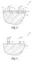
- FIG. 2is a schematic cross-sectional side view of the structure of FIG. 1 after patterning a selectively-definable layer, in accordance with some embodiments of the invention.
- FIG. 3is a schematic cross-sectional side view of the structure of FIG. 2 after etching through a hard mask layer, in accordance with embodiments of the invention.
- FIG. 4is a schematic cross-sectional side view of the structure of FIG. 3 after removing the selectively-definable layer, in accordance with some embodiments of the invention.
- FIG. 5is a schematic, cross-sectional side view of the structure of FIG. 4 after widening spaces between features in the hard mask layer, in accordance with some embodiments of the invention.
- FIG. 6is a schematic, cross-sectional side view of the structure of FIG. 5 after depositing a layer of a solution of self-organizing material, in accordance with some embodiments of the invention.
- FIG. 7is a schematic, cross-sectional side view of the structure of FIG. 6 after self-assembly of the self-organizing material, in accordance with some embodiments of the invention.
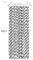
- FIG. 8is a schematic, top plan view of the structure of FIG. 7 showing an arrangement of domains of material resulting from the self-assembly of the self-organizing material, in accordance with some embodiments of the invention.
- FIG. 9is a schematic, cross-sectional side view of the structure of FIG. 7 after selectively removing some domains of self-organizing material to form mandrels, in accordance with some embodiments of the invention.
- FIG. 10is a schematic, cross-sectional side view of the structure of FIG. 9 after depositing a layer of a spacer material, in accordance with some embodiments of the invention.
- FIG. 11is a schematic, cross-sectional side view of the structure of FIG. 10 after a spacer etch, in accordance with some embodiments of the invention.
- FIG. 12is a schematic, cross-sectional side view of the structure of FIG. 11 after removing the mandrels to leave a pattern of free-standing spacers, in accordance with some embodiments of the invention.
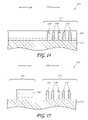
- FIG. 13is a schematic, cross-sectional side view of the structure of FIG. 12 after transferring a pattern formed by the freestanding spacers to an underlying substrate, in accordance with some embodiments of the invention.
- FIG. 14is a schematic, cross-sectional side view of the structure of FIG. 12 after depositing a planarizing layer over the spacers, in accordance with some embodiments of the invention.
- FIG. 15is a schematic, cross-sectional side view of the structure of FIG. 14 after patterning the planarizing layer, in accordance with some embodiments of the invention.
- Block copolymersare formed of two or more chemically distinct blocks. For example, each block may be formed of a different monomer.
- the blocksare immiscible or thermodynamically incompatible, e.g., one block may be polar and the other may be non-polar. Due to thermodynamic effects, the copolymers will self-organize in solution to minimize the energy of the system as a whole; typically, this causes the copolymers to move relative to one another, e.g., so that like blocks aggregate together, thereby forming alternating regions containing each block type or species.
- the blockswill segregate so that non-polar blocks aggregate with other non-polar blocks and polar blocks aggregate with other polar blocks.
- the block copolymersmay be described as a self-organizing material since the blocks can move to form a pattern without active application of an external force to direct the movement of particular individual molecules, although heat may be applied to increase the rate of movement of the population of molecules as a whole.
- the self-organization of block copolymerscan be influenced by topographical features, such as steps on the surface on which the block copolymers are deposited.
- a diblock copolymera copolymer formed of two different block species, may form alternating domains, or regions, which are each formed of a substantially different block species.
- the stepsmay interact with the blocks such that, e.g., each of the alternating regions formed by the blocks is made to form a regular pattern with features oriented parallel to the walls.
- the self-organization of block copolymersmay be guided by photolithographically modifying a surface, without forming steps in the surface, as disclosed in: Stoykovich et al., Science 308, 1442 (2005); Kim et al., Nature 424, 411 (2003); and Edwards et al., Adv. Mater. 16, 1315 (2004). The entire disclosure of each to these references is incorporated by reference herein.
- Such self-organizationcan be useful in forming masks for patterning features during semiconductor fabrication processes. For example, one of the alternating domains may be removed, thereby leaving the material forming the other region to function as a mask.
- the maskmay be used to pattern features such as electrical devices in an underlying semiconductor substrate.
- Methods for forming a copolymer maskare disclosed in U.S. patent application Ser. No. 11/389,581 to Gurtej Sandhu, filed Mar. 23, 2006, entitled Topography Directed Patterning, Attorney Docket No.: MICRON.342A (Micron Ref. No.: 2005-0865); and U.S. patent application Ser. No. 11/445,907 to Gurtej Sandhu, filed Jun.
- the lengths of block copolymersmay be an intrinsic limit to the sizes of domains formed by the blocks of those block copolymers.
- the copolymersmay be chosen with a length that facilitates self-assembly into a desired pattern of domains, and shorter copolymers may not self-assemble as desired.
- Embodiments of the inventionallow for the formation of features smaller than those that may be formed by block polymers alone.
- a self-organizing material formed of different chemical speciesis allowed to organize to form domains composed of like chemical species. Some of those domains are selectively removed to form mandrels, or temporary placeholders.
- a pitch multiplication processis then performed using the mandrels formed from the self-organizing material.
- Features with a pitch smaller than a pitch of the mandrelsare derived from the mandrels.
- spacersare formed on sidewalls of the mandrels and the mandrels are selectively removed. The spacers, or other mask features derived from the spacers, are used as part of a mask to pattern underlying materials, e.g., during the fabrication of integrated circuits.
- Embodiments of the inventionmay form the mask features may be formed without using newer, relatively complex and expensive lithography techniques and the burden on the robustness of photoresist may be reduced.
- spacers or mask features derived from the spacersmay be used as a mask.
- the use of spacersallows the selection of a variety of materials for the spacers, and the materials may be selected for robustness and compatibility with underlying materials used in a process flow.
- the copolymer materialis not used as a mask for patterning underlying layers, the copolymer materials may be selected without regard to, e.g., their robustness and suitability for forming masking layers.
- the copolymer materialmay be selected based upon their self-organizing behavior and suitability for use in mandrels, thereby increasing process latitude.
- the self-organizing behavior of materials such as block copolymersallows the reliable formation of very small features, thereby facilitating the formation of a mask with a very small feature size. For example, features having a critical dimension of about 1 nm to about 100 nm, about 3 nm to about 50 nm or about 5 nm to about 30 may be formed.
- a plurality of mandrelsis formed from self-organizing material, such as block copolymers.
- FIGS. 1-8illustrate a method for self-assembling the self-organizing material into a desired pattern using guides or step features to guide the self-assembly.
- the self-assembly of the self-organizing materialmay be directed by any method known in the art.
- Masking layers 120 , 130may be provided above a substrate 110 to form guides for copolymer self-assembly.
- the materials for the layers 120 , 130 overlying the substrate 110are chosen based upon consideration of the interaction of the layers with block copolymer materials to be used and of the chemistry and process conditions for the various pattern forming and pattern transferring steps discussed herein. For example, because patterns in upper layers are transferred to lower layers, the lower masking layer 130 is chosen so that it can be selectively etched relative to at least some of the other exposed materials.
- a materialis considered selectively, or preferentially, etched when the etch rate for that material is at least about 2-3 times greater, or at least about 10 times greater, or at least about 20 times greater, or at least about 50 times greater than that for surrounding materials.
- the “substrate” to which patterns are transferredmay include a single material, a plurality of layers of different materials, a layer or layers having regions of different materials or different structures in them, etc. These materials may include semiconductors, insulators, conductors, or combinations thereof.
- the substratemay comprise doped polysilicon, a single crystal electrical device active area, a silicide, or a metal layer, such as a tungsten, aluminum or copper layer, or combinations thereof.
- the mask features discussed belowmay directly correspond to the desired placement of conductive features, such as interconnects, in the substrate.
- the substratemay be an insulator and the location of mask features may correspond to the desired location of insulation between conductive features, such as in damascene metallization.
- the mask featuresmay be used as a hard mask to directly etch the substrate, or may be used to transfer a pattern to another underlying layer, e.g., a carbon layer, such as a transparent carbon, layer, which is then used to transfer the pattern to one or more underlying layers, such as the substrate.
- the selectively definable layer 120overlies a hard mask, or etch stop, layer 130 , which overlies the substrate 110 .
- the selectively definable layer 120may be photodefinable, e.g., formed of a photoresist, including any photoresist known in the art.
- the photoresistmay be any photoresist compatible with extreme ultraviolet systems (e.g., 13.4 nm wavelength systems), 157 nm, 193 nm, 248 nm or 365 nm wavelength systems, or 193 nm wavelength immersion systems.
- photoresist materialsinclude argon fluoride (ArF) sensitive photoresist, i.e., photoresist suitable for use with an ArF light source, and krypton fluoride (KrF) sensitive photoresist, i.e., photoresist suitable for use with a KrF light source.
- ArF photoresistsare used with photolithography systems utilizing relatively short wavelength light, e.g., 193 nm.
- KrF photoresistsare used with longer wavelength photolithography systems, such as 248 nm systems.
- the use of self-organizing material and pitch multiplication in embodiments of the inventionmay obviate the need to define extremely small features with expensive, relatively new direct formation techniques such as extreme ultraviolet systems (including 13.4 nm wavelength systems) or electron beam lithographic systems, such systems may also be used, if desired.
- extreme ultraviolet systemsincluding 13.4 nm wavelength systems
- electron beam lithographic systemssuch systems may also be used, if desired.
- maskless lithography, or maskless photolithographymay be used to define the selectively definable layer 120 .
- the layer 120 and any subsequent resist layersmay be formed of a resist that may be patterned by nano-imprint lithography, e.g., by using a mold or mechanical force to form a pattern in the resist.
- the material for the hard mask layer 130may comprise an inorganic material, which is not a polymer. Exemplary materials include silicon oxide (SiO 2 ), silicon nitride, silicon or a dielectric anti-reflective coating (DARC), such as a silicon-rich silicon oxynitride.
- the hard mask layer 130comprises silicon nitride in the illustrated embodiment.
- the material for the hard mask layer 130is selected to interact with the later-deposited self-organizing material to direct the self-assembly of the self-organizing material into a desired pattern.
- the photodefinable layer 120is exposed to radiation through a reticle and then developed to leave a pattern comprising features 122 which are formed of photodefinable material.
- the pitch of the resulting features 122e.g., lines, is equal to the sum of the width of a line 122 and the width of a neighboring space 124 .
- the pitch of the features 122may be, e.g., about 400 nm or less, about 300 nm or less, about 200 nm or less, or about 100 or less.
- the features 122may have a critical dimension of about 140 nm and a pitch of about 280 nm.
- the pattern in the photodefinable layer 120is transferred to the hard mask layer 130 , thereby forming hard mask features 132 in the hard mask layer 130 .
- the pattern transfermay be accomplished using an anisotropic etch, such as an etch using a fluorocarbon plasma, although a wet (isotropic) etch may also be suitable if the hard mask layer 130 is sufficiently thin.
- exemplary fluorocarbon plasma etch chemistriesinclude CFH 3 , CF 2 H 2 , CF 3 H and CF 4 /HBr.
- resist forming the photodefinable layer 120may also be removed, e.g., by plasma ashing.
- the hard mask features 132are trimmed to form guides 134 for copolymer self-assembly.
- the hard mask features 132may be trimmed using a wet or dry etch which selectively etches the hard mask material relative to other exposed materials.
- the trim etchmay be performed using, e.g., a SO 2 /O 2 /Ar plasma. The trim allows the formation of features having smaller critical dimensions than could easily be formed using conventional photolithography.
- hard mask features 132 having a critical dimension of about 140 nm and a pitch of about 280 nmmay be trimmed to form copolymer self-assembly guides 134 having a critical dimension of about 35 nm and the same pitch of about 280 nm.
- the photoresist features 122FIG. 2
- a self-organizing materiale.g., block copolymers
- a self-organizing materialis next applied and allowed to self-assemble to form a mask pattern over the substrate 110 .
- Method for forming self-organized block copolymer patternsare disclosed in Block, IEE Transactions in Nanotechnology, Vol. 3, No. 3, September 2004 and in U.S. patent application Ser. Nos. 11/389,581 and 11/445,907, the entire disclosure of each of which is incorporated by reference herein.
- a film 160 of block copolymer materialis deposited between and over the guides 134 .
- the copolymercomprises blocks of polymer material which may be selectively etched relative to one another and which may self-organize in a desired and predictable manner, e.g., the blocks are immiscible and will segregate under appropriate conditions to form domains predominantly containing a single block species.
- the copolymeris a diblock copolymer, comprising, e.g., polystyrene (PS) and poly-methylmethacrylate (PMMA).
- PSpolystyrene
- PMMApoly-methylmethacrylate
- the diblock copolymersmay be provided dissolved in a solvent, e.g., toluene.
- each diblock copolymer and the ratio of the constituent blocks and monomersmay be chosen to facilitate self-organization and to form organized block domains having desired dimensions.
- a block copolymerhas an intrinsic polymer length scale, the average end-to-end length of the copolymer in film, including any coiling or kinking, which governs the size of the block domains.
- a copolymer solution having longer copolymersmay be used to form larger domains and a copolymer solution having shorter copolymers may be used to form smaller domains.
- the copolymersare selected to provide mandrels that provide a consistent spacing between spacers 175 ( FIG. 12 ).
- the block copolymersare selected to facilitate self-assembly into a desired pattern, the mandrels are trimmed, e.g., by a wet or dry etch, to provide a desired spacing between mandrels.
- the block copolymersmay be deposited by various methods, including, e.g., spin-on coating, spin casting, brush coating or vapor deposition.
- the thickness of the copolymer film 160may be chosen based upon the desired pattern to be formed by the copolymers. It will be appreciated that, up to a particular thickness related to the polymer length scale and the environment in which the polymers are disposed, e.g., the distance between and the height of the guides 134 , the copolymers will typically orient to form alternating, substantially lamellar domains that form parallel lines, as viewed in a top-down view ( FIG. 8 ). Such lamellae may be used to pattern, e.g., interconnects, or the lateral extension of the lamellae may be limited to form isolated features, e.g., transistor gates. Under some conditions, related to the thickness of the film 160 , the polymer length scale and the environment in which the polymers are disposed, the copolymers may orient to form vertically-extending pillars, such as cylinders, or spheres.
- the copolymer film thicknessmay be less than about the length scale of the copolymers forming the film.
- the thickness of the filmsis about 35 nm or less, about 30 nm or less, or about 25 nm or less.
- the thickness of the film 160may be greater than, equal to or less than the height of the guides 134 . As illustrated and discussed further below, a thickness which is greater than the height of the guides 134 may be used to provide a copolymer reservoir. In other embodiments, a thickness which is equal to, or less than the height of the guides 134 may be used to form isolated islands of copolymers between the guides 134 , thereby preventing cross-diffusion of copolymers between the islands.
- the different block speciesare understood to self-aggregate due to thermodynamic considerations in a process similar to the phase separation of materials.
- the self-organizationis guided by the guides 134 , which encourage the constituent blocks of the block copolymers to orient themselves along the length of the guides 134 due to interfacial interactions.
- the self-organizationmay result in a more efficient packing of the copolymer species.
- the free copolymers available for the self-organizationmay be depleted if the copolymer film 160 extends over too large of an expanse, causing an area in the middle of the expanse to be formed without organized copolymers or with poorly organized copolymers.
- the copolymer film 160is sufficiently thick to extend above the guides 134 to provide a reservoir of copolymers for the self-organization which occurs between the guides 134 .
- the distance between the guides 134may be chosen to be sufficiently small to minimize the depletion effect that may occur over large expanses.
- the block copolymers in the copolymer film 160are allowed to self-organize.
- the self-organizationmay be facilitated and accelerated by annealing the partially-fabricated integrated circuit 100 .
- the temperature of the annealmay be chosen to be sufficiently low to prevent adversely affecting the block copolymers or the partially fabricated integrated circuit 100 .
- the annealmay be performed at a temperature of less than about 250° C., less than about 200° C. or about 180° C. in some embodiments.
- the annealmay also be used to cause cross-linking of the copolymers, thereby stabilizing the copolymers for later etching and pattern transfer steps.
- FIG. 7A pattern of lamellae resulting after the anneal is shown in FIG. 7 .
- FIG. 8a top-down view of the partially fabricated integrated circuit of FIG. 7 is shown.
- the PS domains 162can be seen alternating with the PMMA domains 164 . Both domains 162 and 164 extend along the length of the guides 134 .
- the domains 164are selectively removed, leaving behind the domain 162 and the guides 134 (not shown), which can function as mandrels for pitch multiplication. It will be appreciated that the domains 164 may be removed in a single step using a single etch chemistry or may be removed using multiple etches with different etch chemistries. For example, where the domains 164 are formed of PMMA and the domains 162 are formed of PS, the domains 164 may be removed by performing a selective wet etch, e.g., using acetic acid as an etchant. In other embodiments, a dry or anisotropic etch may be appropriate where one of the domains may be etched at a faster rate than the other.
- a selective wet etche.g., using acetic acid as an etchant.
- a dry or anisotropic etchmay be appropriate where one of the domains may be etched at a faster rate than the other.
- the dimensions of the resulting featuresmay vary, depending on the size of the copolymer used and process conditions.
- the resulting patternmay comprise PS domains having a critical dimension of about 50 nm to about 2 nm, about 35 nm or less to about 3 nm, with a pitch of about 100 nm to about 4 nm, or about 70 nm to about 6 nm.
- the domains 162 and/or the guides 134may be removed instead, thereby leaving the domains 164 , with or without the guides 134 .
- the spacer materialmay be any material that may act as a mask for transferring a pattern to an underlying material.
- the spacer materialmay be deposited with good step coverage; 2) may be deposited at a temperature compatible with the mandrels 162 ; and 3) may be selectively etched relative to the mandrels 162 and guides 134 , if present, and the underlying substrate 110 .
- the spacer materialmay be, without limitation, an inorganic material, such as a silicon-containing material, or an organic material, such as a polymer.
- the silicon-containing spacer materialsmay be, without limitation, silicon, silicon oxide and silicon nitride. In the illustrated embodiment, the spacer material is silicon oxide.
- Methods for spacer material depositioninclude atomic layer deposition, e.g., using a self-limiting deposition with a silicon precursor and a subsequent exposure to an oxygen or nitrogen precursor to form silicon oxides and nitrides, respectively.
- ALDmay be performed at relatively low temperatures, e.g., under about 200° C. or under about 100° C., which may prevent thermal damage to underlying thermally sensitive materials.
- ALDmay be used to prevent damage to the polymer material forming the block domains 162 .
- chemical vapor depositionis used to deposit the spacer material.
- the thickness of the layer 170is determined based upon the desired width of the spacers 175 ( FIG. 12 ). For example, in some embodiments, the layer 170 is deposited to a thickness of about 10-80 nm or about 20-50 nm to form spacers of roughly similar widths. The step coverage is about 80% or greater and or about 90% or greater.
- the silicon oxide spacer layer 170is then subjected to an anisotropic etch to remove spacer material from horizontal surfaces 180 of the partially formed integrated circuit 100 .
- an etchalso known as a spacer etch, may be performed using a fluorocarbon plasma, e.g., a CF 4 , CHF 3 and/or NF 3 containing plasma.
- the block domains 162 and any remaining guides 134are removed to leave freestanding spacers 175 .
- the block domains 162 and guides 134may be removed by wet or dry etches that selectively remove those features relative to the spacers 175 .
- the etchesmay also selectively remove the block domains 162 and guides 134 relative to the underlying substrate 110 .
- the same or different etch chemistriesmay be applied. Etch chemistries include, without limitation, a O 2 -based carbon trip etch to remove the PS block domains 162 and a phosphoric acid based wet etch to remove the silicon nitride guides 134 .
- the pitch of the spacers 175is roughly half that of the block domains 162 ( FIG. 9 ) formed by the block copolymers.
- the block domains 162had a pitch of about 200 nm
- spacers 175 having a pitch of about 100 nm or lessmay be formed and where the block domains 162 had a pitch of about 60 nm or less, spacers 175 having a pitch of about 30 nm or less may be formed.
- the spacers 175because the spacers 175 are formed on the sidewalls of the block domains 162 , the spacers 175 generally follow the outline of the block domains 162 and, so, typically form a closed loop.
- the spacers 175form a first pattern 177 . It will be appreciated that higher orders of pitch multiplication can be achieved in some embodiments by using the spacers 175 as mandrels to form other spacers or mask features.
- the pattern 177is transferred to the substrate 110 .
- the pattern transfermay be accomplished using etch chemistries appropriate for selectively etching the material or materials of the substrate 110 relative to the spacers 175 .
- etch chemistriesappropriate for selectively etching the material or materials of the substrate 110 relative to the spacers 175 .
- the skilled artisancan readily determine suitable etch chemistries for substrate materials. It will be appreciated that where the substrate 110 comprises layers of different materials, a succession of different chemistries, e.g., dry-etch chemistries, may be used to successively etch through these different layers, if a single chemistry is not sufficient to etch all the different materials. It will also be appreciated that, depending upon the chemistry or chemistries used, the spacers 175 may be etched. In the illustrated embodiment, the spacers 175 are sufficiently tall to complete the etch of the substrate 110 without being completely worn away.
- the mask overlying the substrate 110including the domain 162 and the guides 134 , are stripped, leaving the patterned substrate 110 .
- the partially fabricated integrated circuit 100is subjected to subsequent processing steps, including forming ancillary electrical devices and electrical interconnects, to form a completed integrated circuit, e.g., a memory chip.
- the copolymersmay be formed of two or more block species.
- the block species of the illustrated embodimentare each formed of a different monomer, the block species may share monomer(s).
- the block speciesmay be formed of different sets of monomers, some of which are the same, or may be formed of the same monomer, but in a different distribution in each block. The different sets of monomers form blocks having different properties which may drive the self-assembly of the copolymers.
- a supplemental layer 180 of self-organizing materialmay be deposited over the block domains 162 and 164 and guides 134 , to vertically extend the pattern defined by those block domains and the guides 134 .
- the self-organizing material forming the supplement layer 180may be a copolymer, such as a block copolymer.
- the material forming the supplemental layer 180is chosen to interact with the block domains 162 and 164 and guides 134 such that the domains 162 , 164 and the guides 134 are able to direct the organization of the self-organizing material.
- the layer 180may also have polar and non-polar block species.
- supplemental block copolymers forming the layer 180are the same as the block copolymers of the film 160 .
- a method for vertically extending a pattern formed of self-organizing materialis disclosed in U.S. patent application Ser. No. 11/445,907 to Gurtej Sandhu, filed Jun. 2, 2006, entitled Topography Based Patterning (Attorney Docket No. MICRON.349A), the entire disclose of which is incorporated herein by reference.
- additional mask patternscan be overlaid the mask pattern 177 ( FIG. 11 ).
- a planarizing materialcan be deposited between and over the spacers 175 and the planarizing material can be patterned to form an additional pattern.
- the additional pattern, forming a combined pattern with the mask pattern 177can be transferred to the underlying substrate 110 .
- the planarizing materialcan be photoresist, such as negative or positive photoresist.
- the photoresistcan be patterned by exposure to radiation to form the additional pattern.
- Negative photoresistcan be used in embodiments in which the features of the mask pattern 177 are very closely spaced, e.g., having a pitch of about 40 nm or less. It has been found that positive photoresist can be difficult to remove between spacers with such small pitches, due to difficulties in completely exposing the photoresist to light. On the other hand increasing the light intensity may undesirably cause polymerization of the photoresist, due to optical amplification by some transparent spacer materials, such as silicon oxide. Negative photoresist does not need to be exposed to light for removal, thereby facilitating the removal of photoresist between spacers and the formation of clean patterns in combination with the mask pattern 177 .
- the hard mask layer 130 overlying the substratemay be omitted.
- the photodefinable materialmay be formed of or replaced by a material which is compatible with the temperatures and other conditions for copolymer self-organization and/or the spacers 175 may be used as a mask for etching the substrate 110 where an etch having sufficient selectivity for the substrate 110 is available.
- additional masking levelsmay be provided over the substrate 110 .
- additional hard mask layerscan be provided between the spacers 175 and the substrate 110 .
- the pattern 177may be transferred to one or more additional hard mask layers before being transferred to the substrate 110 .
- the additional hard mask layersmay be selected to provide higher resistance to etches used for etching the substrate.
- the pattern 177may be transferred to an amorphous carbon layer before being transferred to the substrate 110 .
- Amorphous carbonhas been found to be suitable as a hard mask for etching a variety of silicon-containing materials.
- processing through the mask layersmay involve subjecting layers underlying the mask layers to any semiconductor fabrication process.
- processingmay involve ion implantation, diffusion doping, depositing, oxidizing (particularly with use of a hard mask under the polymer mask), nitridizing, etc. through the mask layers and onto underlying layers.
- the mask layersmay be used as a stop or barrier for chemical mechanical polishing (CMP) or CMP may be performed on any of the layers to allow for both planarization and etching of the underlying layers, as discussed in U.S. patent application Ser. No. 11/216,477, filed Aug. 31, 2005, the entire disclosure of which is incorporated by reference herein.
- embodiments of the inventionmay be applied in various other applications where the formation of patterns with very small features is desired.
- embodiments of the inventionmay be applied to form gratings, disk drives, storage media or templates or masks for other lithography techniques, including X-ray or imprint lithography.
- phase shift photomasksmay be formed by patterning a substrate that has a film stack having phase shifting material coatings.
- a method for patterning a semiconductor substratecomprises providing a layer comprising block copolymers.
- One block of the block copolymersis selectively removed to leave laterally separated mandrels comprising an other block of the block copolymers.
- Spacer materialis blanket depositing on the mandrels.
- the spacer materialis etched to form spacers on sidewalls of the mandrels.
- a pattern defined by the spacersis transferred to the substrate.
- a method for forming a mask for patterning a substratecomprises providing a layer of a self-organizing material. Like chemical species of the self-organizing material are aggregated to form a repeating pattern having domains defined by the chemical species. One of the chemical species is preferentially removed to form spaced apart mandrels Spacers are formed on sidewalls of the mandrels.
- a method for integrated circuit fabricationcomprises exposing a block copolymer layer to a wet etch to define free-standing, regularly-spaced, spaced-apart placeholders in the block copolymer layer. Spacers are formed on sidewalls of the placeholders. A pattern derived from the spacers is transferred to an underlying substrate.
Landscapes
- Engineering & Computer Science (AREA)
- Manufacturing & Machinery (AREA)
- Power Engineering (AREA)
- General Physics & Mathematics (AREA)
- Physics & Mathematics (AREA)
- Computer Hardware Design (AREA)
- Condensed Matter Physics & Semiconductors (AREA)
- Microelectronics & Electronic Packaging (AREA)
- Chemical & Material Sciences (AREA)
- Inorganic Chemistry (AREA)
- General Chemical & Material Sciences (AREA)
- Chemical Kinetics & Catalysis (AREA)
- Exposure Of Semiconductors, Excluding Electron Or Ion Beam Exposure (AREA)
- Drying Of Semiconductors (AREA)
- Formation Of Insulating Films (AREA)
- Semiconductor Memories (AREA)
- Non-Volatile Memory (AREA)
Abstract
Description
- This application is related to U.S. patent application Ser. No. 11/389,581 to Gurtej Sandhu, filed Mar. 23, 2006, entitled Topography Directed Patterning (Attorney Docket No. MICRON.342A) and U.S. patent application Ser. No. 11/445,907 to Gurtej Sandhu, filed Jun. 2, 2006, entitled Topography Based Patterning (Attorney Docket No. MICRON.349A). The entire disclosure of each of these references is incorporated by reference herein.
- 1. Field of the Invention
- This invention relates to mask formation, including printing techniques for integrated circuit fabrication.
- 2. Description of the Related Art
- As a consequence of many factors, including demand for increased portability, computing power, memory capacity and energy efficiency, integrated circuits are continuously being reduced in size. The sizes of the constituent features that form the integrated circuits, e.g., electrical devices and interconnect lines, are also constantly being decreased to facilitate this size reduction.
- The trend of decreasing feature size is evident, for example, in memory circuits or devices such as dynamic random access memories (DRAMs), flash memory, static random access memories (SRAMs), ferroelectric (FE) memories, etc. To take one example, DRAM typically includes millions of identical circuit elements, known as memory cells. A memory cell typically consists of two electrical devices: a storage capacitor and an access field effect transistor. Each memory cell is an addressable location that may store one bit (binary digit) of data. A bit may be written to a cell through the transistor and may be read by sensing charge in the capacitor. Some memory technologies employ elements that can act as both a storage device and a switch (e.g., dendritic memory employing silver-doped chalcogenide glass) and some nonvolatile memories do not require switches for each cell (e.g., magnetoresistive RAM) or incorporate switches into the memory element (e.g., EEPROM for flash memory).
- In another example, flash memory typically includes millions of flash memory cells containing floating gate field effect transistors that may retain a charge. The presence or absence of a charge in the floating gate determines the logic state of the memory cell. A bit may be written to a cell by injecting charge to or removing charge from a cell. Flash memory cells may be connected in different architecture configurations, each with different schemes for reading bits. In a “NOR” architecture configuration, each memory cell is coupled to a bit line and may be read individually. In a “NAND” architecture configuration, memory cells are aligned in a “string” of cells, and an entire bit line is activated to access data in one of the string of cells.
- In general, by decreasing the sizes of the electrical devices that constitute a memory cell and the sizes of the conducting lines that access the memory cells, the memory devices may be made smaller. Additionally, storage capacities may be increased by fitting more memory cells on a given area in the memory devices. The need for reductions in feature sizes, however, is more generally applicable to integrated circuits, including general purpose and specialty processors.
- The continual reduction in feature sizes places ever greater demands on the techniques used to form the features. For example, photolithography is commonly used to pattern these features. Typically, photolithography involves passing light through a reticle and focusing the light onto a photochemically-active photoresist material. Just as a slide has an image to be projected onto a screen, the reticle typically has a pattern to be transferred to a substrate. By directing light or radiation through the reticle, the pattern in the reticle may be focused on the photoresist. The light or radiation causes a chemical change in the illuminated parts of the photoresist, which allows those parts to be selectively retained or removed, depending upon whether positive or negative photoresist is used, relative to parts which were in the shadows. Thus, the exposed and unexposed parts form a pattern in the photoresist.
- Because lithography is typically accomplished by projecting light or radiation onto a surface, the ultimate resolution of a particular lithography technique depends upon factors such as optics and light or radiation wavelength. For example, the ability to focus well-defined patterns onto resist depends upon the size of the features and on the wavelength of the radiation projected through the reticle. It will be appreciated that resolution decreases with increasing wavelength, due, among other things, to diffraction. Thus, shorter wavelength radiation is typically used to form well-resolved features, as the sizes of the features decrease.
- In conjunction with radiation of a particular wavelength, photolithography utilizes photoresist compatible with that radiation. After being developed, the photoresist acts as a mask to transfer a pattern to an underlying material. The photoresist is sufficiently robust to withstand the development step without deforming and is also sufficiently robust to withstand an etch for transferring the mask pattern to an underlying material. As feature sizes decrease, however, the widths of the photoresist mask features also decrease, but typically without a corresponding decrease in the heights of these mask features. Due to the high aspect ratio of these mask features, it may be difficult to maintain the structural integrity of these thin mask features during the development and pattern transfer steps. As a result, the availability of sufficiently robust photoresist materials may limit the ability of photolithography to print features, as those features continue to decrease in size.
- Accordingly, there is a continuing need for high resolution methods to pattern small features.
FIG. 1 is a schematic cross-sectional side view of a substrate with overlying masking layers, in accordance with some embodiments of the invention.FIG. 2 is a schematic cross-sectional side view of the structure ofFIG. 1 after patterning a selectively-definable layer, in accordance with some embodiments of the invention.FIG. 3 is a schematic cross-sectional side view of the structure ofFIG. 2 after etching through a hard mask layer, in accordance with embodiments of the invention.FIG. 4 is a schematic cross-sectional side view of the structure ofFIG. 3 after removing the selectively-definable layer, in accordance with some embodiments of the invention.FIG. 5 is a schematic, cross-sectional side view of the structure ofFIG. 4 after widening spaces between features in the hard mask layer, in accordance with some embodiments of the invention.FIG. 6 is a schematic, cross-sectional side view of the structure ofFIG. 5 after depositing a layer of a solution of self-organizing material, in accordance with some embodiments of the invention.FIG. 7 is a schematic, cross-sectional side view of the structure ofFIG. 6 after self-assembly of the self-organizing material, in accordance with some embodiments of the invention.FIG. 8 is a schematic, top plan view of the structure ofFIG. 7 showing an arrangement of domains of material resulting from the self-assembly of the self-organizing material, in accordance with some embodiments of the invention.FIG. 9 is a schematic, cross-sectional side view of the structure ofFIG. 7 after selectively removing some domains of self-organizing material to form mandrels, in accordance with some embodiments of the invention.FIG. 10 is a schematic, cross-sectional side view of the structure ofFIG. 9 after depositing a layer of a spacer material, in accordance with some embodiments of the invention.FIG. 11 is a schematic, cross-sectional side view of the structure ofFIG. 10 after a spacer etch, in accordance with some embodiments of the invention.FIG. 12 is a schematic, cross-sectional side view of the structure ofFIG. 11 after removing the mandrels to leave a pattern of free-standing spacers, in accordance with some embodiments of the invention.FIG. 13 is a schematic, cross-sectional side view of the structure ofFIG. 12 after transferring a pattern formed by the freestanding spacers to an underlying substrate, in accordance with some embodiments of the invention.FIG. 14 is a schematic, cross-sectional side view of the structure ofFIG. 12 after depositing a planarizing layer over the spacers, in accordance with some embodiments of the invention.FIG. 15 is a schematic, cross-sectional side view of the structure ofFIG. 14 after patterning the planarizing layer, in accordance with some embodiments of the invention.- The ability of block copolymers to self-organize may be used to form mask patterns. Block copolymers are formed of two or more chemically distinct blocks. For example, each block may be formed of a different monomer. The blocks are immiscible or thermodynamically incompatible, e.g., one block may be polar and the other may be non-polar. Due to thermodynamic effects, the copolymers will self-organize in solution to minimize the energy of the system as a whole; typically, this causes the copolymers to move relative to one another, e.g., so that like blocks aggregate together, thereby forming alternating regions containing each block type or species. For example, if the copolymers are formed of polar and non-polar blocks, the blocks will segregate so that non-polar blocks aggregate with other non-polar blocks and polar blocks aggregate with other polar blocks. It will be appreciated that the block copolymers may be described as a self-organizing material since the blocks can move to form a pattern without active application of an external force to direct the movement of particular individual molecules, although heat may be applied to increase the rate of movement of the population of molecules as a whole.
- In addition to interactions between the block species, the self-organization of block copolymers can be influenced by topographical features, such as steps on the surface on which the block copolymers are deposited. For example, a diblock copolymer, a copolymer formed of two different block species, may form alternating domains, or regions, which are each formed of a substantially different block species. When self-organization of block species occurs in the area between the walls of a step, the steps may interact with the blocks such that, e.g., each of the alternating regions formed by the blocks is made to form a regular pattern with features oriented parallel to the walls. In addition, the self-organization of block copolymers may be guided by photolithographically modifying a surface, without forming steps in the surface, as disclosed in: Stoykovich et al., Science 308, 1442 (2005); Kim et al., Nature 424, 411 (2003); and Edwards et al., Adv. Mater. 16, 1315 (2004). The entire disclosure of each to these references is incorporated by reference herein.
- Such self-organization can be useful in forming masks for patterning features during semiconductor fabrication processes. For example, one of the alternating domains may be removed, thereby leaving the material forming the other region to function as a mask. The mask may be used to pattern features such as electrical devices in an underlying semiconductor substrate. Methods for forming a copolymer mask are disclosed in U.S. patent application Ser. No. 11/389,581 to Gurtej Sandhu, filed Mar. 23, 2006, entitled Topography Directed Patterning, Attorney Docket No.: MICRON.342A (Micron Ref. No.: 2005-0865); and U.S. patent application Ser. No. 11/445,907 to Gurtej Sandhu, filed Jun. 2, 2006, entitled Topography Based Patterning (Attorney Docket No. MICRON.349A (Micron Ref. No.: 05-0865), the entire disclosure of each of which is incorporated by reference herein. While self-organizing materials may be used to form relatively small mask features, further decreases in the sizes of the mask features are desired due to the constant miniaturization of integrated circuits.
- Moreover, the lengths of block copolymers may be an intrinsic limit to the sizes of domains formed by the blocks of those block copolymers. For example, the copolymers may be chosen with a length that facilitates self-assembly into a desired pattern of domains, and shorter copolymers may not self-assemble as desired.
- Embodiments of the invention allow for the formation of features smaller than those that may be formed by block polymers alone. In embodiments of the invention, a self-organizing material formed of different chemical species is allowed to organize to form domains composed of like chemical species. Some of those domains are selectively removed to form mandrels, or temporary placeholders. A pitch multiplication process is then performed using the mandrels formed from the self-organizing material. Features with a pitch smaller than a pitch of the mandrels are derived from the mandrels. In some embodiments, spacers are formed on sidewalls of the mandrels and the mandrels are selectively removed. The spacers, or other mask features derived from the spacers, are used as part of a mask to pattern underlying materials, e.g., during the fabrication of integrated circuits.
- Embodiments of the invention may form the mask features may be formed without using newer, relatively complex and expensive lithography techniques and the burden on the robustness of photoresist may be reduced. For example, rather than using relatively soft and structurally delicate photoresist in a mask, spacers or mask features derived from the spacers may be used as a mask. The use of spacers allows the selection of a variety of materials for the spacers, and the materials may be selected for robustness and compatibility with underlying materials used in a process flow. Moreover, because copolymer material is not used as a mask for patterning underlying layers, the copolymer materials may be selected without regard to, e.g., their robustness and suitability for forming masking layers. Rather, the copolymer material may be selected based upon their self-organizing behavior and suitability for use in mandrels, thereby increasing process latitude. Moreover, the self-organizing behavior of materials such as block copolymers allows the reliable formation of very small features, thereby facilitating the formation of a mask with a very small feature size. For example, features having a critical dimension of about 1 nm to about 100 nm, about 3 nm to about 50 nm or about 5 nm to about 30 may be formed.
- Reference will now be made to the Figures, wherein like numerals refer to like parts throughout. It will be appreciated that the Figures are not necessarily drawn to scale.
- In a first phase of methods according to some embodiments, a plurality of mandrels is formed from self-organizing material, such as block copolymers.
FIGS. 1-8 illustrate a method for self-assembling the self-organizing material into a desired pattern using guides or step features to guide the self-assembly. In other embodiments, it will be appreciated that the self-assembly of the self-organizing material may be directed by any method known in the art. - With reference to
FIG. 1 , a cross-sectional side view of a partially formedintegrated circuit 100 is illustrated. Masking layers120,130 may be provided above asubstrate 110 to form guides for copolymer self-assembly. The materials for thelayers substrate 110 are chosen based upon consideration of the interaction of the layers with block copolymer materials to be used and of the chemistry and process conditions for the various pattern forming and pattern transferring steps discussed herein. For example, because patterns in upper layers are transferred to lower layers, thelower masking layer 130 is chosen so that it can be selectively etched relative to at least some of the other exposed materials. It will be appreciated that a material is considered selectively, or preferentially, etched when the etch rate for that material is at least about 2-3 times greater, or at least about 10 times greater, or at least about 20 times greater, or at least about 50 times greater than that for surrounding materials. - It will be appreciated that the “substrate” to which patterns are transferred may include a single material, a plurality of layers of different materials, a layer or layers having regions of different materials or different structures in them, etc. These materials may include semiconductors, insulators, conductors, or combinations thereof. For example, the substrate may comprise doped polysilicon, a single crystal electrical device active area, a silicide, or a metal layer, such as a tungsten, aluminum or copper layer, or combinations thereof. In some embodiments, the mask features discussed below may directly correspond to the desired placement of conductive features, such as interconnects, in the substrate. In other embodiments, the substrate may be an insulator and the location of mask features may correspond to the desired location of insulation between conductive features, such as in damascene metallization. The mask features may be used as a hard mask to directly etch the substrate, or may be used to transfer a pattern to another underlying layer, e.g., a carbon layer, such as a transparent carbon, layer, which is then used to transfer the pattern to one or more underlying layers, such as the substrate.
- With continued reference to
FIG. 1 , the selectivelydefinable layer 120 overlies a hard mask, or etch stop,layer 130, which overlies thesubstrate 110. The selectivelydefinable layer 120 may be photodefinable, e.g., formed of a photoresist, including any photoresist known in the art. For example, the photoresist may be any photoresist compatible with extreme ultraviolet systems (e.g., 13.4 nm wavelength systems), 157 nm, 193 nm, 248 nm or 365 nm wavelength systems, or 193 nm wavelength immersion systems. Examples of photoresist materials include argon fluoride (ArF) sensitive photoresist, i.e., photoresist suitable for use with an ArF light source, and krypton fluoride (KrF) sensitive photoresist, i.e., photoresist suitable for use with a KrF light source. ArF photoresists are used with photolithography systems utilizing relatively short wavelength light, e.g., 193 nm. KrF photoresists are used with longer wavelength photolithography systems, such as 248 nm systems. In addition, while the use of self-organizing material and pitch multiplication in embodiments of the invention may obviate the need to define extremely small features with expensive, relatively new direct formation techniques such as extreme ultraviolet systems (including 13.4 nm wavelength systems) or electron beam lithographic systems, such systems may also be used, if desired. In addition, maskless lithography, or maskless photolithography, may be used to define the selectivelydefinable layer 120. In other embodiments, thelayer 120 and any subsequent resist layers may be formed of a resist that may be patterned by nano-imprint lithography, e.g., by using a mold or mechanical force to form a pattern in the resist. - The material for the
hard mask layer 130 may comprise an inorganic material, which is not a polymer. Exemplary materials include silicon oxide (SiO2), silicon nitride, silicon or a dielectric anti-reflective coating (DARC), such as a silicon-rich silicon oxynitride. Thehard mask layer 130 comprises silicon nitride in the illustrated embodiment. The material for thehard mask layer 130 is selected to interact with the later-deposited self-organizing material to direct the self-assembly of the self-organizing material into a desired pattern. - With reference to
FIG. 2 , thephotodefinable layer 120 is exposed to radiation through a reticle and then developed to leave apattern comprising features 122 which are formed of photodefinable material. It will be appreciated that the pitch of the resultingfeatures 122, e.g., lines, is equal to the sum of the width of aline 122 and the width of a neighboringspace 124. In some embodiments, the pitch of thefeatures 122 may be, e.g., about 400 nm or less, about 300 nm or less, about 200 nm or less, or about 100 or less. In an exemplary embodiment, thefeatures 122 may have a critical dimension of about 140 nm and a pitch of about 280 nm. - With reference to
FIG. 3 , the pattern in thephotodefinable layer 120 is transferred to thehard mask layer 130, thereby forming hard mask features132 in thehard mask layer 130. The pattern transfer may be accomplished using an anisotropic etch, such as an etch using a fluorocarbon plasma, although a wet (isotropic) etch may also be suitable if thehard mask layer 130 is sufficiently thin. Exemplary fluorocarbon plasma etch chemistries include CFH3, CF2H2, CF3H and CF4/HBr. With reference toFIG. 4 , resist forming thephotodefinable layer 120 may also be removed, e.g., by plasma ashing. - With reference to
FIG. 5 , the hard mask features132 (FIG. 4 ) are trimmed to formguides 134 for copolymer self-assembly. The hard mask features132 may be trimmed using a wet or dry etch which selectively etches the hard mask material relative to other exposed materials. The trim etch may be performed using, e.g., a SO2/O2/Ar plasma. The trim allows the formation of features having smaller critical dimensions than could easily be formed using conventional photolithography. For example, hard mask features132 having a critical dimension of about 140 nm and a pitch of about 280 nm may be trimmed to form copolymer self-assembly guides134 having a critical dimension of about 35 nm and the same pitch of about 280 nm. In other embodiments, the photoresist features122 (FIG. 2 ) may be trimmed in addition to, or instead of, the hard mask features132, thereby allowingguides 134 of the desired size to be formed without the need to trim the hard mask features132. - A self-organizing material, e.g., block copolymers, is next applied and allowed to self-assemble to form a mask pattern over the
substrate 110. Method for forming self-organized block copolymer patterns are disclosed in Block, IEE Transactions in Nanotechnology, Vol. 3, No. 3, September 2004 and in U.S. patent application Ser. Nos. 11/389,581 and 11/445,907, the entire disclosure of each of which is incorporated by reference herein. - With reference to
FIG. 6 , afilm 160 of block copolymer material is deposited between and over theguides 134. The copolymer comprises blocks of polymer material which may be selectively etched relative to one another and which may self-organize in a desired and predictable manner, e.g., the blocks are immiscible and will segregate under appropriate conditions to form domains predominantly containing a single block species. In the exemplary illustrated embodiment, the copolymer is a diblock copolymer, comprising, e.g., polystyrene (PS) and poly-methylmethacrylate (PMMA). The diblock copolymers may be provided dissolved in a solvent, e.g., toluene. It will be appreciated that the total size of each diblock copolymer and the ratio of the constituent blocks and monomers may be chosen to facilitate self-organization and to form organized block domains having desired dimensions. For example, it will be appreciated that a block copolymer has an intrinsic polymer length scale, the average end-to-end length of the copolymer in film, including any coiling or kinking, which governs the size of the block domains. A copolymer solution having longer copolymers may be used to form larger domains and a copolymer solution having shorter copolymers may be used to form smaller domains. In some embodiments, the copolymers are selected to provide mandrels that provide a consistent spacing between spacers175 (FIG. 12 ). In other embodiments, the block copolymers are selected to facilitate self-assembly into a desired pattern, the mandrels are trimmed, e.g., by a wet or dry etch, to provide a desired spacing between mandrels. The block copolymers may be deposited by various methods, including, e.g., spin-on coating, spin casting, brush coating or vapor deposition. - The thickness of the
copolymer film 160 may be chosen based upon the desired pattern to be formed by the copolymers. It will be appreciated that, up to a particular thickness related to the polymer length scale and the environment in which the polymers are disposed, e.g., the distance between and the height of theguides 134, the copolymers will typically orient to form alternating, substantially lamellar domains that form parallel lines, as viewed in a top-down view (FIG. 8 ). Such lamellae may be used to pattern, e.g., interconnects, or the lateral extension of the lamellae may be limited to form isolated features, e.g., transistor gates. Under some conditions, related to the thickness of thefilm 160, the polymer length scale and the environment in which the polymers are disposed, the copolymers may orient to form vertically-extending pillars, such as cylinders, or spheres. - For forming lamellae, the copolymer film thickness may be less than about the length scale of the copolymers forming the film. For example, where the copolymer length scale is about 35 nm, the thickness of the films is about 35 nm or less, about 30 nm or less, or about 25 nm or less.
- It will be appreciated that the thickness of the
film 160 may be greater than, equal to or less than the height of theguides 134. As illustrated and discussed further below, a thickness which is greater than the height of theguides 134 may be used to provide a copolymer reservoir. In other embodiments, a thickness which is equal to, or less than the height of theguides 134 may be used to form isolated islands of copolymers between theguides 134, thereby preventing cross-diffusion of copolymers between the islands. - While the invention is not bound by theory, it will be appreciated that the different block species are understood to self-aggregate due to thermodynamic considerations in a process similar to the phase separation of materials. The self-organization is guided by the
guides 134, which encourage the constituent blocks of the block copolymers to orient themselves along the length of theguides 134 due to interfacial interactions. It will be appreciated that the self-organization may result in a more efficient packing of the copolymer species. As a result, in some cases, the free copolymers available for the self-organization may be depleted if thecopolymer film 160 extends over too large of an expanse, causing an area in the middle of the expanse to be formed without organized copolymers or with poorly organized copolymers. Thus, in some embodiments, thecopolymer film 160 is sufficiently thick to extend above theguides 134 to provide a reservoir of copolymers for the self-organization which occurs between theguides 134. In addition, the distance between theguides 134 may be chosen to be sufficiently small to minimize the depletion effect that may occur over large expanses. - With reference to
FIG. 7 , the block copolymers in thecopolymer film 160 are allowed to self-organize. The self-organization may be facilitated and accelerated by annealing the partially-fabricatedintegrated circuit 100. The temperature of the anneal may be chosen to be sufficiently low to prevent adversely affecting the block copolymers or the partially fabricated integratedcircuit 100. The anneal may be performed at a temperature of less than about 250° C., less than about 200° C. or about 180° C. in some embodiments. The anneal may also be used to cause cross-linking of the copolymers, thereby stabilizing the copolymers for later etching and pattern transfer steps. - A pattern of lamellae resulting after the anneal is shown in
FIG. 7 .Domains 162 of one block species, e.g., PS, anddomains 164 of the other block species, e.g., PMMA, alternate between theguides 134. It will be appreciated that the sizes of the block domains are determined by the sizes of the block species forming them. - With reference to
FIG. 8 , a top-down view of the partially fabricated integrated circuit ofFIG. 7 is shown. ThePS domains 162 can be seen alternating with thePMMA domains 164. Bothdomains guides 134. - With reference to
FIG. 9 , thedomains 164 are selectively removed, leaving behind thedomain 162 and the guides134 (not shown), which can function as mandrels for pitch multiplication. It will be appreciated that thedomains 164 may be removed in a single step using a single etch chemistry or may be removed using multiple etches with different etch chemistries. For example, where thedomains 164 are formed of PMMA and thedomains 162 are formed of PS, thedomains 164 may be removed by performing a selective wet etch, e.g., using acetic acid as an etchant. In other embodiments, a dry or anisotropic etch may be appropriate where one of the domains may be etched at a faster rate than the other. It will be appreciated that the dimensions of the resulting features may vary, depending on the size of the copolymer used and process conditions. In some embodiments, the resulting pattern may comprise PS domains having a critical dimension of about 50 nm to about 2 nm, about 35 nm or less to about 3 nm, with a pitch of about 100 nm to about 4 nm, or about 70 nm to about 6 nm. It will be appreciated that in other embodiments, thedomains 162 and/or theguides 134 may be removed instead, thereby leaving thedomains 164, with or without theguides 134. - Next, with reference to
FIG. 10 , alayer 170 of spacer material is blanket deposited conformally over exposed surfaces, including thesubstrate 110. The spacer material may be any material that may act as a mask for transferring a pattern to an underlying material. The spacer material: 1) may be deposited with good step coverage; 2) may be deposited at a temperature compatible with themandrels 162; and 3) may be selectively etched relative to themandrels 162 and guides134, if present, and theunderlying substrate 110. The spacer material may be, without limitation, an inorganic material, such as a silicon-containing material, or an organic material, such as a polymer. The silicon-containing spacer materials may be, without limitation, silicon, silicon oxide and silicon nitride. In the illustrated embodiment, the spacer material is silicon oxide. - Methods for spacer material deposition include atomic layer deposition, e.g., using a self-limiting deposition with a silicon precursor and a subsequent exposure to an oxygen or nitrogen precursor to form silicon oxides and nitrides, respectively. ALD may be performed at relatively low temperatures, e.g., under about 200° C. or under about 100° C., which may prevent thermal damage to underlying thermally sensitive materials. For example, ALD may be used to prevent damage to the polymer material forming the
block domains 162. In other embodiments, chemical vapor deposition is used to deposit the spacer material. - The thickness of the
layer 170 is determined based upon the desired width of the spacers175 (FIG. 12 ). For example, in some embodiments, thelayer 170 is deposited to a thickness of about 10-80 nm or about 20-50 nm to form spacers of roughly similar widths. The step coverage is about 80% or greater and or about 90% or greater. - With reference to
FIG. 11 , the siliconoxide spacer layer 170 is then subjected to an anisotropic etch to remove spacer material fromhorizontal surfaces 180 of the partially formedintegrated circuit 100. Such an etch, also known as a spacer etch, may be performed using a fluorocarbon plasma, e.g., a CF4, CHF3and/or NF3containing plasma. - With reference to
FIG. 12 , theblock domains 162 and any remainingguides 134 are removed to leavefreestanding spacers 175. Theblock domains 162 and guides134 may be removed by wet or dry etches that selectively remove those features relative to thespacers 175. The etches may also selectively remove theblock domains 162 and guides134 relative to theunderlying substrate 110. Depending upon the material forming theblock domains 162 and theguides 134, the same or different etch chemistries may be applied. Etch chemistries include, without limitation, a O2-based carbon trip etch to remove thePS block domains 162 and a phosphoric acid based wet etch to remove the silicon nitride guides134. - Thus, pitch-multiplied mask features have been formed. In the illustrated embodiment, the pitch of the
spacers 175 is roughly half that of the block domains162 (FIG. 9 ) formed by the block copolymers. For example, where theblock domains 162 had a pitch of about 200 nm,spacers 175 having a pitch of about 100 nm or less may be formed and where theblock domains 162 had a pitch of about 60 nm or less,spacers 175 having a pitch of about 30 nm or less may be formed. It will be appreciated that because thespacers 175 are formed on the sidewalls of theblock domains 162, thespacers 175 generally follow the outline of theblock domains 162 and, so, typically form a closed loop. Thespacers 175 form afirst pattern 177. It will be appreciated that higher orders of pitch multiplication can be achieved in some embodiments by using thespacers 175 as mandrels to form other spacers or mask features. - With reference to
FIG. 13 , thepattern 177 is transferred to thesubstrate 110. The pattern transfer may be accomplished using etch chemistries appropriate for selectively etching the material or materials of thesubstrate 110 relative to thespacers 175. The skilled artisan can readily determine suitable etch chemistries for substrate materials. It will be appreciated that where thesubstrate 110 comprises layers of different materials, a succession of different chemistries, e.g., dry-etch chemistries, may be used to successively etch through these different layers, if a single chemistry is not sufficient to etch all the different materials. It will also be appreciated that, depending upon the chemistry or chemistries used, thespacers 175 may be etched. In the illustrated embodiment, thespacers 175 are sufficiently tall to complete the etch of thesubstrate 110 without being completely worn away. - With reference to
FIG. 14 , the mask overlying thesubstrate 110, including thedomain 162 and theguides 134, are stripped, leaving the patternedsubstrate 110. After the pattern transfer, the partially fabricated integratedcircuit 100 is subjected to subsequent processing steps, including forming ancillary electrical devices and electrical interconnects, to form a completed integrated circuit, e.g., a memory chip. - It will be appreciated that various modifications of the illustrated embodiments are possible. For example, while discussed in the context of diblock copolymers for ease of illustration and discussion, the copolymers may be formed of two or more block species. In addition, while the block species of the illustrated embodiment are each formed of a different monomer, the block species may share monomer(s). For example, the block species may be formed of different sets of monomers, some of which are the same, or may be formed of the same monomer, but in a different distribution in each block. The different sets of monomers form blocks having different properties which may drive the self-assembly of the copolymers.
- In some embodiments, a
supplemental layer 180 of self-organizing material may be deposited over theblock domains guides 134. The self-organizing material forming thesupplement layer 180 may be a copolymer, such as a block copolymer. The material forming thesupplemental layer 180 is chosen to interact with theblock domains domains guides 134 are able to direct the organization of the self-organizing material. For example, where theblock domains layer 180 may also have polar and non-polar block species. In some embodiments, supplemental block copolymers forming thelayer 180 are the same as the block copolymers of thefilm 160. A method for vertically extending a pattern formed of self-organizing material is disclosed in U.S. patent application Ser. No. 11/445,907 to Gurtej Sandhu, filed Jun. 2, 2006, entitled Topography Based Patterning (Attorney Docket No. MICRON.349A), the entire disclose of which is incorporated herein by reference. - It will be appreciated that, before or after transferring the
mask pattern 177 to thesubstrate 110, additional mask patterns can be overlaid the mask pattern177 (FIG. 11 ). For example, a planarizing material can be deposited between and over thespacers 175 and the planarizing material can be patterned to form an additional pattern. The additional pattern, forming a combined pattern with themask pattern 177, can be transferred to theunderlying substrate 110. With reference toFIG. 15 , the planarizing material can be photoresist, such as negative or positive photoresist. With reference toFIG. 16 , the photoresist can be patterned by exposure to radiation to form the additional pattern. Negative photoresist can be used in embodiments in which the features of themask pattern 177 are very closely spaced, e.g., having a pitch of about 40 nm or less. It has been found that positive photoresist can be difficult to remove between spacers with such small pitches, due to difficulties in completely exposing the photoresist to light. On the other hand increasing the light intensity may undesirably cause polymerization of the photoresist, due to optical amplification by some transparent spacer materials, such as silicon oxide. Negative photoresist does not need to be exposed to light for removal, thereby facilitating the removal of photoresist between spacers and the formation of clean patterns in combination with themask pattern 177. - In some embodiments, the
hard mask layer 130 overlying the substrate may be omitted. For example, the photodefinable material may be formed of or replaced by a material which is compatible with the temperatures and other conditions for copolymer self-organization and/or thespacers 175 may be used as a mask for etching thesubstrate 110 where an etch having sufficient selectivity for thesubstrate 110 is available. - In some other embodiments, additional masking levels may be provided over the
substrate 110. For example, additional hard mask layers can be provided between thespacers 175 and thesubstrate 110. Thepattern 177 may be transferred to one or more additional hard mask layers before being transferred to thesubstrate 110. The additional hard mask layers may be selected to provide higher resistance to etches used for etching the substrate. For example, thepattern 177 may be transferred to an amorphous carbon layer before being transferred to thesubstrate 110. Amorphous carbon has been found to be suitable as a hard mask for etching a variety of silicon-containing materials. - Also, while “processing” through a mask layer may encompass etching an underlying layer, processing through the mask layers may involve subjecting layers underlying the mask layers to any semiconductor fabrication process. For example, processing may involve ion implantation, diffusion doping, depositing, oxidizing (particularly with use of a hard mask under the polymer mask), nitridizing, etc. through the mask layers and onto underlying layers. In addition, the mask layers may be used as a stop or barrier for chemical mechanical polishing (CMP) or CMP may be performed on any of the layers to allow for both planarization and etching of the underlying layers, as discussed in U.S. patent application Ser. No. 11/216,477, filed Aug. 31, 2005, the entire disclosure of which is incorporated by reference herein.
- In addition, while the illustrated embodiments may be applied to fabricate integrated circuits, embodiments of the invention may be applied in various other applications where the formation of patterns with very small features is desired. For example, embodiments of the invention may be applied to form gratings, disk drives, storage media or templates or masks for other lithography techniques, including X-ray or imprint lithography. For example, phase shift photomasks may be formed by patterning a substrate that has a film stack having phase shifting material coatings.
- Consequently, it will be appreciated from the description herein that the invention includes various embodiments. For example, according to some embodiments of the invention, a method for patterning a semiconductor substrate is provided. The method comprises providing a layer comprising block copolymers. One block of the block copolymers is selectively removed to leave laterally separated mandrels comprising an other block of the block copolymers. Spacer material is blanket depositing on the mandrels. The spacer material is etched to form spacers on sidewalls of the mandrels. A pattern defined by the spacers is transferred to the substrate.
- According to other embodiments the invention, a method for forming a mask for patterning a substrate is provided. The method comprises providing a layer of a self-organizing material. Like chemical species of the self-organizing material are aggregated to form a repeating pattern having domains defined by the chemical species. One of the chemical species is preferentially removed to form spaced apart mandrels Spacers are formed on sidewalls of the mandrels.
- According to yet other embodiments of the invention, a method for integrated circuit fabrication is provided. The method comprises exposing a block copolymer layer to a wet etch to define free-standing, regularly-spaced, spaced-apart placeholders in the block copolymer layer. Spacers are formed on sidewalls of the placeholders. A pattern derived from the spacers is transferred to an underlying substrate.
- In addition to the above disclosure, it will also be appreciated by those skilled in the art that various omissions, additions and modifications may be made to the methods and structures described above without departing from the scope of the invention. All such modifications and changes are intended to fall within the scope of the invention, as defined by the appended claims.
Claims (35)
Priority Applications (8)
| Application Number | Priority Date | Filing Date | Title |
|---|---|---|---|
| US11/757,846US7923373B2 (en) | 2007-06-04 | 2007-06-04 | Pitch multiplication using self-assembling materials |
| PCT/US2008/063943WO2008150673A1 (en) | 2007-06-04 | 2008-05-16 | Pitch multiplication using self-assembling materials |
| CN2008800187311ACN101681812B (en) | 2007-06-04 | 2008-05-16 | Pitch multiplication using self-assembling materials |
| JP2010511238AJP5110409B2 (en) | 2007-06-04 | 2008-05-16 | Pitch multiplication using self-organizing materials |
| KR1020097027395AKR101547706B1 (en) | 2007-06-04 | 2008-05-16 | Pitch multiplication using self-assembling materials |
| EP08755741.9AEP2165355B1 (en) | 2007-06-04 | 2008-05-16 | Pitch multiplication using self-assembling materials |
| TW097119748ATWI360161B (en) | 2007-06-04 | 2008-05-28 | Pitch multiplication using self-assembling materia |
| US12/908,206US10515801B2 (en) | 2007-06-04 | 2010-10-20 | Pitch multiplication using self-assembling materials |
Applications Claiming Priority (1)
| Application Number | Priority Date | Filing Date | Title |
|---|---|---|---|
| US11/757,846US7923373B2 (en) | 2007-06-04 | 2007-06-04 | Pitch multiplication using self-assembling materials |
Related Child Applications (1)
| Application Number | Title | Priority Date | Filing Date |
|---|---|---|---|
| US12/908,206ContinuationUS10515801B2 (en) | 2007-06-04 | 2010-10-20 | Pitch multiplication using self-assembling materials |
Publications (2)
| Publication Number | Publication Date |
|---|---|
| US20080299774A1true US20080299774A1 (en) | 2008-12-04 |
| US7923373B2 US7923373B2 (en) | 2011-04-12 |
Family
ID=39689121
Family Applications (2)
| Application Number | Title | Priority Date | Filing Date |
|---|---|---|---|
| US11/757,846Active2029-12-04US7923373B2 (en) | 2007-06-04 | 2007-06-04 | Pitch multiplication using self-assembling materials |
| US12/908,206Active2028-05-02US10515801B2 (en) | 2007-06-04 | 2010-10-20 | Pitch multiplication using self-assembling materials |
Family Applications After (1)
| Application Number | Title | Priority Date | Filing Date |
|---|---|---|---|
| US12/908,206Active2028-05-02US10515801B2 (en) | 2007-06-04 | 2010-10-20 | Pitch multiplication using self-assembling materials |
Country Status (7)
| Country | Link |
|---|---|
| US (2) | US7923373B2 (en) |
| EP (1) | EP2165355B1 (en) |
| JP (1) | JP5110409B2 (en) |
| KR (1) | KR101547706B1 (en) |
| CN (1) | CN101681812B (en) |
| TW (1) | TWI360161B (en) |
| WO (1) | WO2008150673A1 (en) |
Cited By (42)
| Publication number | Priority date | Publication date | Assignee | Title |
|---|---|---|---|---|
| US20080182402A1 (en)* | 2007-01-26 | 2008-07-31 | International Business Machines Corporation | Sub-lithographic interconnect patterning using self-assembling polymers |
| US20080318381A1 (en)* | 2007-06-20 | 2008-12-25 | George Matamis | Methods of forming high density semiconductor devices using recursive spacer technique |
| US20090179002A1 (en)* | 2008-01-14 | 2009-07-16 | International Business Machines Corporation | Method of forming polymer features by directed self-assembly of block copolymers |
| US20090305497A1 (en)* | 2008-06-05 | 2009-12-10 | Mitsuhiro Omura | Method for fabricating semiconductor device |
| US7700441B2 (en) | 2006-02-02 | 2010-04-20 | Micron Technology, Inc. | Methods of forming field effect transistors, methods of forming field effect transistor gates, methods of forming integrated circuitry comprising a transistor gate array and circuitry peripheral to the gate array, and methods of forming integrated circuitry comprising a transistor gate array including first gates and second grounded isolation gates |
| US20100120255A1 (en)* | 2008-11-13 | 2010-05-13 | Matsunga Kentaro | Semiconductor device manufacturing method |
| US7772632B2 (en) | 2006-08-21 | 2010-08-10 | Micron Technology, Inc. | Memory arrays and methods of fabricating memory arrays |
| US7825462B2 (en) | 2004-09-01 | 2010-11-02 | Micron Technology, Inc. | Transistors |
| US7867851B2 (en) | 2005-08-30 | 2011-01-11 | Micron Technology, Inc. | Methods of forming field effect transistors on substrates |
| US7897460B2 (en) | 2005-03-25 | 2011-03-01 | Micron Technology, Inc. | Methods of forming recessed access devices associated with semiconductor constructions |
| US7944743B2 (en) | 2006-09-07 | 2011-05-17 | Micron Technology, Inc. | Methods of making a semiconductor memory device |
| US20110281085A1 (en)* | 2010-05-14 | 2011-11-17 | Tada Yasuhiko | Polymer thin film, patterned media, production methods thereof, and surface modifying agents |
| WO2011152959A3 (en)* | 2010-06-03 | 2012-05-10 | Micron Technology , Inc. | Methods of forming patterns on substrates |
| US8399920B2 (en) | 2005-07-08 | 2013-03-19 | Werner Juengling | Semiconductor device comprising a transistor gate having multiple vertically oriented sidewalls |
| US8551823B2 (en) | 2006-07-17 | 2013-10-08 | Micron Technology, Inc. | Methods of forming lines of capacitorless one transistor DRAM cells, methods of patterning substrates, and methods of forming two conductive lines |
| US8722535B2 (en) | 2012-06-04 | 2014-05-13 | Kabushiki Kaisha Toshiba | Pattern forming method, mold and data processing method |
| US8734904B2 (en) | 2010-11-30 | 2014-05-27 | International Business Machines Corporation | Methods of forming topographical features using segregating polymer mixtures |
| US8772166B2 (en) | 2007-11-01 | 2014-07-08 | Micron Technology, Inc. | Spacer process for on pitch contacts and related structures |
| US8871648B2 (en) | 2007-12-06 | 2014-10-28 | Micron Technology, Inc. | Method for forming high density patterns |
| US8871646B2 (en) | 2008-11-24 | 2014-10-28 | Micron Technology, Inc. | Methods of forming a masking pattern for integrated circuits |
| US20140370712A1 (en)* | 2013-06-12 | 2014-12-18 | Eunsung KIM | Methods of forming a pattern and devices formed by the same |
| US8928111B2 (en) | 2008-07-03 | 2015-01-06 | Micron Technology, Inc. | Transistor with high breakdown voltage having separated drain extensions |
| US8932960B2 (en) | 2007-12-18 | 2015-01-13 | Micron Technology, Inc. | Methods for isolating portions of a loop of pitch-multiplied material and related structures |
| US8952502B2 (en)* | 2012-11-19 | 2015-02-10 | Taiwan Semiconductor Manufacturing Company Limited | Semiconductor patterning |
| US9048194B2 (en) | 2008-03-21 | 2015-06-02 | Micron Technology, Inc. | Method for selectively modifying spacing between pitch multiplied structures |
| US20150170905A1 (en)* | 2007-07-30 | 2015-06-18 | Micron Technology, Inc. | Methods for device fabrication using pitch reduction and related devices |
| KR101535227B1 (en)* | 2008-12-31 | 2015-07-08 | 삼성전자주식회사 | Method for forming fine pattern using block copolymer |
| US20150255283A1 (en)* | 2013-01-04 | 2015-09-10 | Taiwan Semiconductor Manufacturing Company Limited | Photo resist trimmed line end space |
| US20160042970A1 (en)* | 2013-04-16 | 2016-02-11 | Tokyo Electron Limited | Pattern forming method |
| US9330914B2 (en) | 2013-10-08 | 2016-05-03 | Micron Technology, Inc. | Methods of forming line patterns in substrates |
| US9412591B2 (en) | 2007-07-31 | 2016-08-09 | Micron Technology, Inc. | Process of semiconductor fabrication with mask overlay on pitch multiplied features and associated structures |
| US20160284560A1 (en)* | 2015-03-24 | 2016-09-29 | Kabushiki Kaisha Toshiba | Pattern forming method |
| US20160343575A1 (en)* | 2015-05-19 | 2016-11-24 | Samsung Electronics Co., Ltd. | Method of fabricating pattern structure |
| US9576817B1 (en)* | 2015-12-03 | 2017-02-21 | International Business Machines Corporation | Pattern decomposition for directed self assembly patterns templated by sidewall image transfer |
| US9684236B1 (en)* | 2016-03-17 | 2017-06-20 | Taiwan Semiconductor Manufacturing Co., Ltd. | Method of patterning a film layer |
| US9696628B2 (en)* | 2015-09-11 | 2017-07-04 | Kabushiki Kaisha Toshiba | Pattern forming method |
| US9812333B2 (en)* | 2013-12-26 | 2017-11-07 | Korea Advanced Institute Of Science And Technology | Nanoscale patterning method and integrated device for electronic apparatus manufactured therefrom |
| US20180082850A1 (en)* | 2016-08-09 | 2018-03-22 | International Business Machines Corporation | Self-aligned single dummy fin cut with tight pitch |
| US10153173B2 (en) | 2015-02-17 | 2018-12-11 | Lg Chem, Ltd. | Method for wet etching of block copolymer self-assembly pattern |
| US10515801B2 (en) | 2007-06-04 | 2019-12-24 | Micron Technology, Inc. | Pitch multiplication using self-assembling materials |
| WO2020014352A1 (en)* | 2018-07-11 | 2020-01-16 | Tokyo Electron Limited | Methods to reduce gouging for core removal processes using thermal decomposition materials |
| US20230223259A1 (en)* | 2022-01-07 | 2023-07-13 | Nanya Technology Corporation | Method for preparing semiconductor device structure having features of different depths |
Families Citing this family (54)
| Publication number | Priority date | Publication date | Assignee | Title |
|---|---|---|---|---|
| US8575021B2 (en)* | 2004-11-22 | 2013-11-05 | Intermolecular, Inc. | Substrate processing including a masking layer |
| US7723009B2 (en) | 2006-06-02 | 2010-05-25 | Micron Technology, Inc. | Topography based patterning |
| KR20100039847A (en)* | 2007-06-15 | 2010-04-16 | 어플라이드 머티어리얼스, 인코포레이티드 | Oxygen sacvd to form sacrificial oxide liners in substrate gaps |
| JP5238556B2 (en)* | 2009-03-10 | 2013-07-17 | 東京エレクトロン株式会社 | Substrate processing method |
| FR2975823B1 (en)* | 2011-05-27 | 2014-11-21 | Commissariat Energie Atomique | METHOD FOR MAKING A PATTERN ON THE SURFACE OF A BLOCK OF A SUBSTRATE USING BLOCK COPOLYMERS |
| US9177910B2 (en) | 2012-04-18 | 2015-11-03 | Micron Technology, Inc. | Interconnect structures for integrated circuits and their formation |
| US9005877B2 (en) | 2012-05-15 | 2015-04-14 | Tokyo Electron Limited | Method of forming patterns using block copolymers and articles thereof |
| US9298870B1 (en)* | 2012-05-16 | 2016-03-29 | International Business Machines Corporation | Method for designing topographic patterns for directing the formation of self-assembled domains at specified locations on substrates |
| KR20140029050A (en) | 2012-08-31 | 2014-03-10 | 삼성전자주식회사 | Method of forming pattern |
| JP6019966B2 (en)* | 2012-09-10 | 2016-11-02 | 大日本印刷株式会社 | Pattern formation method |
| JP6088803B2 (en)* | 2012-11-16 | 2017-03-01 | 株式会社日立ハイテクノロジーズ | Image processing apparatus, pattern generation method using self-organized lithography technology, and computer program |
| KR101993255B1 (en)* | 2013-01-07 | 2019-06-26 | 삼성전자주식회사 | Method of forming contact holes |
| JP6136271B2 (en)* | 2013-01-08 | 2017-05-31 | 大日本印刷株式会社 | Manufacturing method of imprint mold |
| JP6127517B2 (en)* | 2013-01-08 | 2017-05-17 | 大日本印刷株式会社 | Manufacturing method of imprint mold |
| US8969207B2 (en) | 2013-03-13 | 2015-03-03 | Globalfoundries Inc. | Methods of forming a masking layer for patterning underlying structures |
| US9147574B2 (en)* | 2013-03-14 | 2015-09-29 | Tokyo Electron Limited | Topography minimization of neutral layer overcoats in directed self-assembly applications |
| US20140273534A1 (en) | 2013-03-14 | 2014-09-18 | Tokyo Electron Limited | Integration of absorption based heating bake methods into a photolithography track system |
| US8975009B2 (en) | 2013-03-14 | 2015-03-10 | Tokyo Electron Limited | Track processing to remove organic films in directed self-assembly chemo-epitaxy applications |
| US8980538B2 (en) | 2013-03-14 | 2015-03-17 | Tokyo Electron Limited | Chemi-epitaxy in directed self-assembly applications using photo-decomposable agents |
| US8906802B2 (en) | 2013-03-15 | 2014-12-09 | Globalfoundries Inc. | Methods of forming trench/via features in an underlying structure using a process that includes a masking layer formed by a directed self-assembly process |
| US9136110B2 (en) | 2013-03-15 | 2015-09-15 | Tokyo Electron Limited | Multi-step bake apparatus and method for directed self-assembly lithography control |
| JP5802233B2 (en) | 2013-03-27 | 2015-10-28 | 株式会社東芝 | Pattern formation method |
| KR20140137734A (en)* | 2013-05-23 | 2014-12-03 | 삼성디스플레이 주식회사 | Method of manufacturing reflective polarizer plate and method fo manufacturing in-cell reflective polarizer plate |
| US9437443B2 (en) | 2013-06-12 | 2016-09-06 | Globalfoundries Inc. | Low-temperature sidewall image transfer process using ALD metals, metal oxides and metal nitrides |
| KR102394998B1 (en) | 2013-09-04 | 2022-05-04 | 도쿄엘렉트론가부시키가이샤 | Uv-assisted stripping of hardened photoresist to create chemical templates for directed self-assembly |
| US9793137B2 (en) | 2013-10-20 | 2017-10-17 | Tokyo Electron Limited | Use of grapho-epitaxial directed self-assembly applications to precisely cut logic lines |
| US9349604B2 (en) | 2013-10-20 | 2016-05-24 | Tokyo Electron Limited | Use of topography to direct assembly of block copolymers in grapho-epitaxial applications |
| US10642152B2 (en) | 2013-11-08 | 2020-05-05 | Asml Netherlands B.V | Methodology to generate a guiding template for directed self-assembly |
| CN103560109A (en)* | 2013-11-13 | 2014-02-05 | 宁波市鄞州科启动漫工业技术有限公司 | Method for forming multiple contact holes |
| US9177797B2 (en)* | 2013-12-04 | 2015-11-03 | Taiwan Semiconductor Manufacturing Company, Ltd. | Lithography using high selectivity spacers for pitch reduction |
| US9064901B1 (en) | 2013-12-23 | 2015-06-23 | International Business Machines Corporation | Fin density control of multigate devices through sidewall image transfer processes |
| KR20150101875A (en) | 2014-02-27 | 2015-09-04 | 삼성전자주식회사 | Method of forming fine pattern using block copolymers |
| US10096696B2 (en)* | 2014-06-03 | 2018-10-09 | Micron Technology, Inc. | Field effect transistors having a fin |
| US9406522B2 (en) | 2014-07-24 | 2016-08-02 | Applied Materials, Inc. | Single platform, multiple cycle spacer deposition and etch |
| JP6173989B2 (en) | 2014-08-29 | 2017-08-02 | 東芝メモリ株式会社 | Pattern formation method |
| KR102302704B1 (en) | 2014-09-02 | 2021-09-15 | 삼성전자주식회사 | Patterns for forming a mask and methods of forming holes using the same and methods of manufacturing |
| JP2017531921A (en)* | 2014-10-08 | 2017-10-26 | アプライド マテリアルズ インコーポレイテッドApplied Materials,Incorporated | Accurate critical dimension control using two-layer ALD |
| US20160233159A1 (en)* | 2015-02-10 | 2016-08-11 | Qualcomm Incorporated | Integrated circuit device including multiple via connectors and a metal structure having a ladder shape |
| US9738765B2 (en) | 2015-02-19 | 2017-08-22 | International Business Machines Corporation | Hybrid topographical and chemical pre-patterns for directed self-assembly of block copolymers |
| KR102306669B1 (en) | 2015-05-12 | 2021-09-29 | 삼성전자주식회사 | Method of forming pattern and method of manufacturing integrated circuit device using the same |
| US9812325B2 (en)* | 2015-09-03 | 2017-11-07 | Tokyo Electron Limited | Method for modifying spacer profile |
| US10020196B2 (en)* | 2015-09-24 | 2018-07-10 | Tokyo Electron Limited | Methods of forming etch masks for sub-resolution substrate patterning |
| CN108369899B (en) | 2015-11-20 | 2023-11-17 | 东京毅力科创株式会社 | Method of forming an etch mask for sub-resolution substrate patterning |
| US20180323078A1 (en)* | 2015-12-24 | 2018-11-08 | Intel Corporation | Pitch division using directed self-assembly |
| US9947597B2 (en) | 2016-03-31 | 2018-04-17 | Tokyo Electron Limited | Defectivity metrology during DSA patterning |
| JP6183519B2 (en)* | 2016-08-26 | 2017-08-23 | 大日本印刷株式会社 | Method for producing template for nanoimprint |
| US10832908B2 (en)* | 2016-11-11 | 2020-11-10 | Lam Research Corporation | Self-aligned multi-patterning process flow with ALD gapfill spacer mask |
| TWI721231B (en)* | 2016-11-16 | 2021-03-11 | 日商東京威力科創股份有限公司 | Methods of sub-resolution substrate patterning |
| US10546748B2 (en) | 2017-02-17 | 2020-01-28 | Lam Research Corporation | Tin oxide films in semiconductor device manufacturing |
| KR102630349B1 (en) | 2018-01-30 | 2024-01-29 | 램 리써치 코포레이션 | Tin oxide mandrels in patterning |
| KR102801539B1 (en)* | 2019-06-14 | 2025-05-02 | 삼성전자주식회사 | Method of forming a semiconductor device using a thermally-decomposable layer, a semiconductor fabrication apparatus and the semiconductor device |
| US11551938B2 (en) | 2019-06-27 | 2023-01-10 | Lam Research Corporation | Alternating etch and passivation process |
| US11581264B2 (en)* | 2019-08-21 | 2023-02-14 | Micron Technology, Inc. | Electronic devices comprising overlay marks, memory devices comprising overlay marks, and related methods |
| US11862668B2 (en)* | 2021-07-02 | 2024-01-02 | Micron Technology, Inc. | Single-crystal transistors for memory devices |
Citations (97)
| Publication number | Priority date | Publication date | Assignee | Title |
|---|---|---|---|---|
| US2006A (en)* | 1841-03-16 | Clamp for crimping leather | ||
| US4432132A (en)* | 1981-12-07 | 1984-02-21 | Bell Telephone Laboratories, Incorporated | Formation of sidewall oxide layers by reactive oxygen ion etching to define submicron features |
| US4502914A (en)* | 1982-11-13 | 1985-03-05 | International Business Machines Corporation | Method of making structures with dimensions in the sub-micrometer range |
| US4508579A (en)* | 1981-03-30 | 1985-04-02 | International Business Machines Corporation | Lateral device structures using self-aligned fabrication techniques |
| US4648937A (en)* | 1985-10-30 | 1987-03-10 | International Business Machines Corporation | Method of preventing asymmetric etching of lines in sub-micrometer range sidewall images transfer |
| US4776922A (en)* | 1987-10-30 | 1988-10-11 | International Business Machines Corporation | Formation of variable-width sidewall structures |
| US4838991A (en)* | 1987-10-30 | 1989-06-13 | International Business Machines Corporation | Process for defining organic sidewall structures |
| US5013680A (en)* | 1990-07-18 | 1991-05-07 | Micron Technology, Inc. | Process for fabricating a DRAM array having feature widths that transcend the resolution limit of available photolithography |
| US5053105A (en)* | 1990-07-19 | 1991-10-01 | Micron Technology, Inc. | Process for creating an etch mask suitable for deep plasma etches employing self-aligned silicidation of a metal layer masked with a silicon dioxide template |
| US5117027A (en)* | 1990-10-31 | 1992-05-26 | Huls Aktiengesellschaft | Process for the preparation of organosilanes containing methacryloyloxy or acryloyloxy groups |
| US5328810A (en)* | 1990-05-07 | 1994-07-12 | Micron Technology, Inc. | Method for reducing, by a factor or 2-N, the minimum masking pitch of a photolithographic process |
| US5330879A (en)* | 1992-07-16 | 1994-07-19 | Micron Technology, Inc. | Method for fabrication of close-tolerance lines and sharp emission tips on a semiconductor wafer |
| US5514885A (en)* | 1986-10-09 | 1996-05-07 | Myrick; James J. | SOI methods and apparatus |
| US5670794A (en)* | 1994-10-07 | 1997-09-23 | Micron Technology, Inc. | Thin film transistors |
| US5753546A (en)* | 1995-06-30 | 1998-05-19 | Hyundai Electronics Industries Co., Ltd. | Method for fabricating metal oxide field effect transistors |
| US5772905A (en)* | 1995-11-15 | 1998-06-30 | Regents Of The University Of Minnesota | Nanoimprint lithography |
| US5789320A (en)* | 1996-04-23 | 1998-08-04 | International Business Machines Corporation | Plating of noble metal electrodes for DRAM and FRAM |
| US5795830A (en)* | 1995-06-06 | 1998-08-18 | International Business Machines Corporation | Reducing pitch with continuously adjustable line and space dimensions |
| US5899746A (en)* | 1995-09-08 | 1999-05-04 | Sony Corporation | Method of forming pattern |
| US5948470A (en)* | 1997-04-28 | 1999-09-07 | Harrison; Christopher | Method of nanoscale patterning and products made thereby |
| US6010946A (en)* | 1996-08-21 | 2000-01-04 | Nec Corporation | Semiconductor device with isolation insulating film tapered and method of manufacturing the same |
| US6042998A (en)* | 1993-09-30 | 2000-03-28 | The University Of New Mexico | Method and apparatus for extending spatial frequencies in photolithography images |
| US6057573A (en)* | 1998-05-27 | 2000-05-02 | Vanguard International Semiconductor Corporation | Design for high density memory with relaxed metal pitch |
| US6063688A (en)* | 1997-09-29 | 2000-05-16 | Intel Corporation | Fabrication of deep submicron structures and quantum wire transistors using hard-mask transistor width definition |
| US6071789A (en)* | 1998-11-10 | 2000-06-06 | Vanguard International Semiconductor Corporation | Method for simultaneously fabricating a DRAM capacitor and metal interconnections |
| US6110837A (en)* | 1999-04-28 | 2000-08-29 | Worldwide Semiconductor Manufacturing Corp. | Method for forming a hard mask of half critical dimension |
| US6207490B1 (en)* | 1997-12-11 | 2001-03-27 | Samsung Electronics Co., Ltd. | Semiconductor device and method for fabricating the same |
| US6211044B1 (en)* | 1999-04-12 | 2001-04-03 | Advanced Micro Devices | Process for fabricating a semiconductor device component using a selective silicidation reaction |
| US6288454B1 (en)* | 1999-05-13 | 2001-09-11 | Lsi Logic Corporation | Semiconductor wafer having a layer-to-layer alignment mark and method for fabricating the same |
| US6291334B1 (en)* | 1997-12-19 | 2001-09-18 | Applied Materials, Inc. | Etch stop layer for dual damascene process |
| US6297554B1 (en)* | 2000-03-10 | 2001-10-02 | United Microelectronics Corp. | Dual damascene interconnect structure with reduced parasitic capacitance |
| US6335257B1 (en)* | 2000-09-29 | 2002-01-01 | Vanguard International Semiconductor Corporation | Method of making pillar-type structure on semiconductor substrate |
| US6348380B1 (en)* | 2000-08-25 | 2002-02-19 | Micron Technology, Inc. | Use of dilute steam ambient for improvement of flash devices |
| US6362057B1 (en)* | 1999-10-26 | 2002-03-26 | Motorola, Inc. | Method for forming a semiconductor device |
| US20020042198A1 (en)* | 2000-09-20 | 2002-04-11 | Bjarni Bjarnason | Method in etching of a substrate |
| US20020045308A1 (en)* | 1996-11-01 | 2002-04-18 | Werner Juengling | Semiconductor processing methods of forming a plurality of capacitors on a substrate, bit line contacts and method of forming bit line contacts |
| US6383907B1 (en)* | 1999-09-08 | 2002-05-07 | Sony Corporation | Process for fabricating a semiconductor device |
| US20020063110A1 (en)* | 2000-11-30 | 2002-05-30 | Cantell Marc W. | Etching of hard masks |
| US20020068243A1 (en)* | 2000-12-04 | 2002-06-06 | Jiunn-Ren Hwang | Method of forming opening in wafer layer |
| US6423474B1 (en)* | 2000-03-21 | 2002-07-23 | Micron Technology, Inc. | Use of DARC and BARC in flash memory processing |
| US20020127810A1 (en)* | 2000-05-29 | 2002-09-12 | Fujitsu Limited | Semiconductor device and method for fabricating the same |
| US6455372B1 (en)* | 2000-08-14 | 2002-09-24 | Micron Technology, Inc. | Nucleation for improved flash erase characteristics |
| US6514884B2 (en)* | 1998-02-06 | 2003-02-04 | Semiconductor Process Laboratory Co., Ltd. | Method for reforming base surface, method for manufacturing semiconductor device and equipment for manufacturing the same |
| US6522584B1 (en)* | 2001-08-02 | 2003-02-18 | Micron Technology, Inc. | Programming methods for multi-level flash EEPROMs |
| US6534243B1 (en)* | 2000-10-23 | 2003-03-18 | Advanced Micro Devices, Inc. | Chemical feature doubling process |
| US6548396B2 (en)* | 1998-07-23 | 2003-04-15 | Applied Materials, Inc. | Method of producing an interconnect structure for an integrated circuit |
| US6559017B1 (en)* | 2002-06-13 | 2003-05-06 | Advanced Micro Devices, Inc. | Method of using amorphous carbon as spacer material in a disposable spacer process |
| US6566280B1 (en)* | 2002-08-26 | 2003-05-20 | Intel Corporation | Forming polymer features on a substrate |
| US6573030B1 (en)* | 2000-02-17 | 2003-06-03 | Applied Materials, Inc. | Method for depositing an amorphous carbon layer |
| US20030109102A1 (en)* | 2001-10-24 | 2003-06-12 | Hiroshi Kujirai | Method of manufacturing semiconductor device and semiconductor device |
| US6602779B1 (en)* | 2002-05-13 | 2003-08-05 | Taiwan Semiconductor Manufacturing Co., Ltd | Method for forming low dielectric constant damascene structure while employing carbon doped silicon oxide planarizing stop layer |
| US20030170995A1 (en)* | 1995-11-15 | 2003-09-11 | Chou Stephen Y. | Method and apparatus for high density nanostructures |
| US6673684B1 (en)* | 2002-07-31 | 2004-01-06 | Advanced Micro Devices, Inc. | Use of diamond as a hard mask material |
| US20040017989A1 (en)* | 2002-07-23 | 2004-01-29 | So Daniel W. | Fabricating sub-resolution structures in planar lightwave devices |
| US6686245B1 (en)* | 2002-12-20 | 2004-02-03 | Motorola, Inc. | Vertical MOSFET with asymmetric gate structure |
| US6689695B1 (en)* | 2002-06-28 | 2004-02-10 | Taiwan Semiconductor Manufacturing Company | Multi-purpose composite mask for dual damascene patterning |
| US6706571B1 (en)* | 2002-10-22 | 2004-03-16 | Advanced Micro Devices, Inc. | Method for forming multiple structures in a semiconductor device |
| US6709807B2 (en)* | 1999-12-02 | 2004-03-23 | Axcelis Technologies, Inc. | Process for reducing edge roughness in patterned photoresist |
| US6734107B2 (en)* | 2002-06-12 | 2004-05-11 | Macronix International Co., Ltd. | Pitch reduction in semiconductor fabrication |
| US6744094B2 (en)* | 2001-08-24 | 2004-06-01 | Micron Technology Inc. | Floating gate transistor with horizontal gate layers stacked next to vertical body |
| US6773998B1 (en)* | 2003-05-20 | 2004-08-10 | Advanced Micro Devices, Inc. | Modified film stack and patterning strategy for stress compensation and prevention of pattern distortion in amorphous carbon gate patterning |
| US6867116B1 (en)* | 2003-11-10 | 2005-03-15 | Macronix International Co., Ltd. | Fabrication method of sub-resolution pitch for integrated circuits |
| US6875703B1 (en)* | 2004-01-20 | 2005-04-05 | International Business Machines Corporation | Method for forming quadruple density sidewall image transfer (SIT) structures |
| US6893972B2 (en)* | 2001-08-31 | 2005-05-17 | Infineon Technologies Ag | Process for sidewall amplification of resist structures and for the production of structures having reduced structure size |
| US20050112886A1 (en)* | 2001-12-28 | 2005-05-26 | Kabushiki Kaisha Toshiba | Light-emitting device and method for manufacturing the same |
| US6911400B2 (en)* | 2002-11-05 | 2005-06-28 | International Business Machines Corporation | Nonlithographic method to produce self-aligned mask, articles produced by same and compositions for same |
| US20050142497A1 (en)* | 2003-12-26 | 2005-06-30 | Samsung Electronics Co., Ltd. | Method of forming a pattern in a semiconductor device and method of forming a gate using the same |
| US20050153562A1 (en)* | 2004-01-08 | 2005-07-14 | Toshiharu Furukawa | Method of independent P and N gate length control of FET device made by sidewall image transfer technique |
| US6924191B2 (en)* | 2002-06-20 | 2005-08-02 | Applied Materials, Inc. | Method for fabricating a gate structure of a field effect transistor |
| US20050167394A1 (en)* | 2004-01-30 | 2005-08-04 | Wei Liu | Techniques for the use of amorphous carbon (APF) for various etch and litho integration scheme |
| US6926953B2 (en)* | 2001-10-05 | 2005-08-09 | Wisconsin Alumni Research Foundation | Guided self-assembly of block copolymer films on interferometrically nanopatterned substrates |
| US20060003182A1 (en)* | 2004-07-01 | 2006-01-05 | Lane Richard H | Method for forming controlled geometry hardmasks including subresolution elements and resulting structures |
| US20060024940A1 (en)* | 2004-07-28 | 2006-02-02 | International Business Machines Corporation | Borderless contact structures |
| US20060024945A1 (en)* | 2004-07-29 | 2006-02-02 | Hynix Semiconductor, Inc. | Method for fabricating semiconductor device using amorphous carbon layer as sacrificial hard mask |
| US20060046484A1 (en)* | 2004-09-02 | 2006-03-02 | Abatchev Mirzafer K | Method for integrated circuit fabrication using pitch multiplication |
| US20060046161A1 (en)* | 2004-08-31 | 2006-03-02 | Zhiping Yin | Prevention of photoresist scumming |
| US7015124B1 (en)* | 2003-04-28 | 2006-03-21 | Advanced Micro Devices, Inc. | Use of amorphous carbon for gate patterning |
| US7074668B1 (en)* | 2004-12-16 | 2006-07-11 | Hynix Semiconductor Inc. | Capacitor of semiconductor device and method for forming the same |
| US20060172540A1 (en)* | 2005-02-03 | 2006-08-03 | Jeffrey Marks | Reduction of feature critical dimensions using multiple masks |
| US20060189150A1 (en)* | 2005-02-23 | 2006-08-24 | Hynix Semiconductor Inc. | Composition for an organic hard mask and method for forming a pattern on a semiconductor device using the same |
| US20070026672A1 (en)* | 2005-07-29 | 2007-02-01 | Micron Technology, Inc. | Pitch doubled circuit layout |
| US7183597B2 (en)* | 2000-03-01 | 2007-02-27 | Intel Corporation | Quantum wire gate device and method of making same |
| US7183205B2 (en)* | 2004-06-08 | 2007-02-27 | Macronix International Co., Ltd. | Method of pitch dimension shrinkage |
| US20070048674A1 (en)* | 2005-09-01 | 2007-03-01 | Wells David H | Methods for forming arrays of small, closely spaced features |
| US20070049030A1 (en)* | 2005-09-01 | 2007-03-01 | Sandhu Gurtej S | Pitch multiplication spacers and methods of forming the same |
| US20070049032A1 (en)* | 2005-09-01 | 2007-03-01 | Mirzafer Abatchev | Protective coating for planarization |
| US20070045712A1 (en)* | 2005-09-01 | 2007-03-01 | Haller Gordon A | Memory cell layout and process flow |
| US20070049040A1 (en)* | 2005-03-15 | 2007-03-01 | Micron Technology, Inc., A Corporation | Multiple deposition for integration of spacers in pitch multiplication process |
| US20070049035A1 (en)* | 2005-08-31 | 2007-03-01 | Tran Luan C | Method of forming pitch multipled contacts |
| US20070049011A1 (en)* | 2005-09-01 | 2007-03-01 | Micron Technology, Inc., A Corporation | Method of forming isolated features using pitch multiplication |
| US20070050748A1 (en)* | 2005-08-30 | 2007-03-01 | Micron Technology, Inc., A Corporation | Method and algorithm for random half pitched interconnect layout with constant spacing |
| US7208379B2 (en)* | 2004-11-29 | 2007-04-24 | Texas Instruments Incorporated | Pitch multiplication process |
| US20070210449A1 (en)* | 2006-03-07 | 2007-09-13 | Dirk Caspary | Memory device and an array of conductive lines and methods of making the same |
| US20070215960A1 (en)* | 2004-03-19 | 2007-09-20 | The Regents Of The University Of California | Methods for Fabrication of Positional and Compositionally Controlled Nanostructures on Substrate |
| US20070215874A1 (en)* | 2006-03-17 | 2007-09-20 | Toshiharu Furukawa | Layout and process to contact sub-lithographic structures |
| US20080057687A1 (en)* | 2006-09-01 | 2008-03-06 | Ngimat Co., A Georgia Corporation | Selective area deposition and devices formed therefrom |
| US20080054350A1 (en)* | 2006-09-06 | 2008-03-06 | International Business Machines Corporation | Vertical field effect transistor arrays and methods for fabrication thereof |
Family Cites Families (1294)
| Publication number | Priority date | Publication date | Assignee | Title |
|---|---|---|---|---|
| BE755502A (en) | 1969-09-09 | 1971-03-01 | Basf Ag | FORMYL-3-BUTANEDIOL-1,2 BISMONOCARBOXYLATES AND PROCESS FOR THEIR PREPARATION |
| US3731287A (en) | 1971-07-02 | 1973-05-01 | Gen Instrument Corp | Single device memory system having shift register output characteristics |
| US3941629A (en) | 1974-04-11 | 1976-03-02 | General Motors Corporation | Diaphragm formation on silicon substrate |
| JPS51147280A (en) | 1975-06-13 | 1976-12-17 | Hitachi Ltd | Semiconductor device |
| GB1527894A (en) | 1975-10-15 | 1978-10-11 | Mullard Ltd | Methods of manufacturing electronic devices |
| JPS53148389A (en) | 1977-05-31 | 1978-12-23 | Fujitsu Ltd | Manufacture for semiconductor device |
| US4139442A (en) | 1977-09-13 | 1979-02-13 | International Business Machines Corporation | Reactive ion etching method for producing deep dielectric isolation in silicon |
| US4234362A (en) | 1978-11-03 | 1980-11-18 | International Business Machines Corporation | Method for forming an insulator between layers of conductive material |
| JPS55148464A (en) | 1979-05-08 | 1980-11-19 | Chiyou Lsi Gijutsu Kenkyu Kumiai | Mos semiconductor device and its manufacture |
| JPS5681974A (en) | 1979-12-07 | 1981-07-04 | Toshiba Corp | Manufacture of mos type semiconductor device |
| JPS5748237A (en) | 1980-09-05 | 1982-03-19 | Nec Corp | Manufacture of 2n doubling pattern |
| US4333964A (en) | 1980-09-15 | 1982-06-08 | General Electric Company | Method of making integrated circuits |
| US4517729A (en) | 1981-07-27 | 1985-05-21 | American Microsystems, Incorporated | Method for fabricating MOS device with self-aligned contacts |
| US4422885A (en) | 1981-12-18 | 1983-12-27 | Ncr Corporation | Polysilicon-doped-first CMOS process |
| US4419809A (en) | 1981-12-30 | 1983-12-13 | International Business Machines Corporation | Fabrication process of sub-micrometer channel length MOSFETs |
| JPS58220464A (en) | 1982-06-17 | 1983-12-22 | Fujitsu Ltd | Semiconductor memory device |
| US4554570A (en) | 1982-06-24 | 1985-11-19 | Rca Corporation | Vertically integrated IGFET device |
| US4508757A (en) | 1982-12-20 | 1985-04-02 | International Business Machines Corporation | Method of manufacturing a minimum bird's beak recessed oxide isolation structure |
| JPS59208783A (en) | 1983-05-12 | 1984-11-27 | Seiko Instr & Electronics Ltd | thin film transistor |
| KR920010461B1 (en) | 1983-09-28 | 1992-11-28 | 가부시끼가이샤 히다찌세이사꾸쇼 | Semiconductor Memory and Manufacturing Method |
| US4472459A (en) | 1983-10-24 | 1984-09-18 | Rca Corporation | Local oxidation of silicon substrate using LPCVD silicon nitride |
| US4716131A (en) | 1983-11-28 | 1987-12-29 | Nec Corporation | Method of manufacturing semiconductor device having polycrystalline silicon layer with metal silicide film |
| US4570325A (en) | 1983-12-16 | 1986-02-18 | Kabushiki Kaisha Toshiba | Manufacturing a field oxide region for a semiconductor device |
| US4569032A (en) | 1983-12-23 | 1986-02-04 | At&T Bell Laboratories | Dynamic CMOS logic circuits for implementing multiple AND-functions |
| JPS60167349A (en) | 1984-02-09 | 1985-08-30 | Nec Corp | Semiconductor integrated circuit device |
| US4549927A (en) | 1984-06-29 | 1985-10-29 | International Business Machines Corporation | Method of selectively exposing the sidewalls of a trench and its use to the forming of a metal silicide substrate contact for dielectric filled deep trench isolated devices |
| JPH0626251B2 (en) | 1984-11-27 | 1994-04-06 | アメリカン テレフオン アンド テレグラフ カムパニ− | Groove transistor |
| US4551910A (en) | 1984-11-27 | 1985-11-12 | Intel Corporation | MOS Isolation processing |
| US4615762A (en) | 1985-04-30 | 1986-10-07 | Rca Corporation | Method for thinning silicon |
| US4984039A (en) | 1985-05-03 | 1991-01-08 | Texas Instruments Incorporated | Tapered trench structure and process |
| JPS6245058A (en) | 1985-08-22 | 1987-02-27 | Nec Corp | Semiconductor device and its manufacture |
| US4630356A (en) | 1985-09-19 | 1986-12-23 | International Business Machines Corporation | Method of forming recessed oxide isolation with reduced steepness of the birds' neck |
| US4675984A (en) | 1985-09-19 | 1987-06-30 | Rca Corporation | Method of exposing only the top surface of a mesa |
| GB8528967D0 (en) | 1985-11-25 | 1986-01-02 | Plessey Co Plc | Semiconductor device manufacture |
| US4789560A (en) | 1986-01-08 | 1988-12-06 | Advanced Micro Devices, Inc. | Diffusion stop method for forming silicon oxide during the fabrication of IC devices |
| EP0238690B1 (en)* | 1986-03-27 | 1991-11-06 | International Business Machines Corporation | Process for forming sidewalls |
| GB2190789B (en) | 1986-04-17 | 1990-05-09 | Plessey Co Plc | System for optically coupling components of integrated circuits |
| US4722910A (en) | 1986-05-27 | 1988-02-02 | Analog Devices, Inc. | Partially self-aligned metal contact process |
| US4835741A (en) | 1986-06-02 | 1989-05-30 | Texas Instruments Incorporated | Frasable electrically programmable read only memory cell using a three dimensional trench floating gate |
| US4829018A (en) | 1986-06-27 | 1989-05-09 | Wahlstrom Sven E | Multilevel integrated circuits employing fused oxide layers |
| US4746630A (en) | 1986-09-17 | 1988-05-24 | Hewlett-Packard Company | Method for producing recessed field oxide with improved sidewall characteristics |
| US4983544A (en) | 1986-10-20 | 1991-01-08 | International Business Machines Corporation | Silicide bridge contact process |
| US5160491A (en) | 1986-10-21 | 1992-11-03 | Texas Instruments Incorporated | Method of making a vertical MOS transistor |
| US4757026A (en) | 1986-11-04 | 1988-07-12 | Intel Corporation | Source drain doping technique |
| US4849371A (en) | 1986-12-22 | 1989-07-18 | Motorola Inc. | Monocrystalline semiconductor buried layers for electrical contacts to semiconductor devices |
| JPS63183691A (en) | 1987-01-26 | 1988-07-29 | Mitsubishi Electric Corp | semiconductor storage device |
| US5149669A (en) | 1987-03-06 | 1992-09-22 | Seiko Instruments Inc. | Method of forming an isolation region in a semiconductor device |
| JPS63260166A (en) | 1987-04-17 | 1988-10-27 | Oki Electric Ind Co Ltd | Semiconductor memory device and manufacture thereof |
| JPS6413290A (en) | 1987-07-07 | 1989-01-18 | Oki Electric Ind Co Ltd | Semiconductor memory |
| JPS6428876A (en) | 1987-07-23 | 1989-01-31 | Matsushita Electric Industrial Co Ltd | Manufacture of superconducting 3-terminal element |
| JPS6435916A (en) | 1987-07-31 | 1989-02-07 | Hitachi Ltd | Formation of fine pattern |
| JPS6442132A (en)* | 1987-08-10 | 1989-02-14 | Hitachi Ltd | Formation of pattern |
| JPS6467945A (en) | 1987-09-08 | 1989-03-14 | Mitsubishi Electric Corp | Wiring layer formed on buried dielectric and manufacture thereof |
| JPH01100948A (en) | 1987-10-14 | 1989-04-19 | Fujitsu Ltd | Manufacturing method of semiconductor device |
| JPH01119028A (en) | 1987-10-30 | 1989-05-11 | Nec Corp | Manufacture of semiconductor device |
| JPH0626202B2 (en) | 1987-10-30 | 1994-04-06 | インターナシヨナル・ビジネス・マシーンズ・コーポレーシヨン | Patterning method |
| JPH01125858A (en) | 1987-11-10 | 1989-05-18 | Fujitsu Ltd | Semiconductor device and manufacture thereof |
| US4818714A (en) | 1987-12-02 | 1989-04-04 | Advanced Micro Devices, Inc. | Method of making a high performance MOS device having LDD regions with graded junctions |
| FR2625044B1 (en) | 1987-12-18 | 1990-08-31 | Commissariat Energie Atomique | TRANSISTOR MOS WITH END OF DIELECTRIC INTERFACE OF GRID / RAISED SUBSTRATE AND MANUFACTURING METHOD THEREOF |
| US4979004A (en) | 1988-01-29 | 1990-12-18 | Texas Instruments Incorporated | Floating gate memory cell and device |
| US4931409A (en) | 1988-01-30 | 1990-06-05 | Kabushiki Kaisha Toshiba | Method of manufacturing semiconductor device having trench isolation |
| US4992838A (en) | 1988-02-29 | 1991-02-12 | Texas Instruments Incorporated | Vertical MOS transistor with threshold voltage adjustment |
| JPH01227468A (en) | 1988-03-08 | 1989-09-11 | Oki Electric Ind Co Ltd | Semiconductor storage device |
| US4871688A (en) | 1988-05-02 | 1989-10-03 | Micron Technology, Inc. | Sequence of etching polysilicon in semiconductor memory devices |
| US5252504A (en) | 1988-05-02 | 1993-10-12 | Micron Technology, Inc. | Reverse polysilicon CMOS fabrication |
| US5103276A (en) | 1988-06-01 | 1992-04-07 | Texas Instruments Incorporated | High performance composed pillar dram cell |
| US5014110A (en) | 1988-06-03 | 1991-05-07 | Mitsubishi Denki Kabushiki Kaisha | Wiring structures for semiconductor memory device |
| FR2633101B1 (en) | 1988-06-16 | 1992-02-07 | Commissariat Energie Atomique | PHOTODIODE AND MATRIX OF PHOTODIODES ON HGCDTE AND METHODS OF MAKING SAME |
| US5015595A (en) | 1988-09-09 | 1991-05-14 | Advanced Micro Devices, Inc. | Method of making a high performance MOS device having both P- and N-LDD regions using single photoresist mask |
| JPH0294477A (en) | 1988-09-30 | 1990-04-05 | Toshiba Corp | Semiconductor device and manufacture thereof |
| US5346834A (en) | 1988-11-21 | 1994-09-13 | Hitachi, Ltd. | Method for manufacturing a semiconductor device and a semiconductor memory device |
| JP2734027B2 (en) | 1988-11-25 | 1998-03-30 | ソニー株式会社 | Wiring formation method |
| JPH02219253A (en) | 1989-02-20 | 1990-08-31 | Sumitomo Metal Ind Ltd | Manufacture of semiconductor integrated circuit device |
| US4959325A (en) | 1989-02-24 | 1990-09-25 | Micron Technology, Inc. | Reduction of electric field effect in the bird's beak region of a DRAM cell following expansion of active region through local encroachment reduction |
| US4965221A (en) | 1989-03-15 | 1990-10-23 | Micron Technology, Inc. | Spacer isolation method for minimizing parasitic sidewall capacitance and creating fully recessed field oxide regions |
| US5108938A (en) | 1989-03-21 | 1992-04-28 | Grumman Aerospace Corporation | Method of making a trench gate complimentary metal oxide semiconductor transistor |
| JPH0823672A (en) | 1989-05-18 | 1996-01-23 | Hirotami Nakano | Switching power unit and its insulating method |
| US5021355A (en) | 1989-05-22 | 1991-06-04 | International Business Machines Corporation | Method of fabricating cross-point lightly-doped drain-source trench transistor |
| JPH033375A (en) | 1989-05-31 | 1991-01-09 | Fujitsu Ltd | Manufacture of oxide superconducting device |
| JP2512216B2 (en) | 1989-08-01 | 1996-07-03 | 松下電器産業株式会社 | Method for manufacturing semiconductor device |
| US5316962A (en) | 1989-08-15 | 1994-05-31 | Matsushita Electric Industrial Co., Ltd. | Method of producing a semiconductor device having trench capacitors and vertical switching transistors |
| US5181089A (en) | 1989-08-15 | 1993-01-19 | Matsushita Electric Industrial Co., Ltd. | Semiconductor memory device and a method for producing the same |
| JP2508288B2 (en) | 1989-08-30 | 1996-06-19 | 三菱電機株式会社 | Semiconductor memory device |
| US5012306A (en) | 1989-09-22 | 1991-04-30 | Board Of Regents, The University Of Texas System | Hot-carrier suppressed sub-micron MISFET device |
| US5024959A (en) | 1989-09-25 | 1991-06-18 | Motorola, Inc. | CMOS process using doped glass layer |
| US5497497A (en) | 1989-11-03 | 1996-03-05 | Compaq Computer Corp. | Method and apparatus for resetting multiple processors using a common ROM |
| JPH03155165A (en) | 1989-11-14 | 1991-07-03 | Toshiba Corp | Semiconductor device and manufacture thereof |
| IT1236601B (en) | 1989-12-22 | 1993-03-18 | Sgs Thomson Microelectronics | INTEGRATED SEMICONDUCTOR DEVICE OF EPROM TYPE WITH METAL CONNECTIONS OF SOURCE AND PROCEDURE FOR ITS MANUFACTURE. |
| US5296401A (en) | 1990-01-11 | 1994-03-22 | Mitsubishi Denki Kabushiki Kaisha | MIS device having p channel MOS device and n channel MOS device with LDD structure and manufacturing method thereof |
| JPH03219677A (en) | 1990-01-24 | 1991-09-27 | Fujitsu Ltd | semiconductor equipment |
| US5218218A (en) | 1990-02-01 | 1993-06-08 | Mitsubishi Denki Kabushiki Kaisha | Semiconductor device and manufacturing method thereof |
| US5387555A (en) | 1992-09-03 | 1995-02-07 | Harris Corporation | Bonded wafer processing with metal silicidation |
| JPH03239332A (en) | 1990-02-16 | 1991-10-24 | Fujitsu Ltd | Manufacture of semiconductor device |
| US5057449A (en) | 1990-03-26 | 1991-10-15 | Micron Technology, Inc. | Process for creating two thicknesses of gate oxide within a dynamic random access memory |
| US5252845A (en) | 1990-04-02 | 1993-10-12 | Electronics And Telecommunications Research Institute | Trench DRAM cell with vertical transistor |
| US5107459A (en) | 1990-04-20 | 1992-04-21 | International Business Machines Corporation | Stacked bit-line architecture for high density cross-point memory cell array |
| JPH0834302B2 (en) | 1990-04-21 | 1996-03-29 | 株式会社東芝 | Semiconductor memory device |
| JPH0414253A (en) | 1990-05-02 | 1992-01-20 | Sony Corp | Dynamic ram and its manufacture |
| JPH0414255A (en) | 1990-05-07 | 1992-01-20 | Toshiba Corp | MOS type semiconductor device |
| EP0456318B1 (en) | 1990-05-11 | 2001-08-22 | Koninklijke Philips Electronics N.V. | CMOS process utilizing disposable silicon nitride spacers for making lightly doped drain transistors |
| US5071782A (en) | 1990-06-28 | 1991-12-10 | Texas Instruments Incorporated | Vertical memory cell array and method of fabrication |
| JP2792211B2 (en) | 1990-07-06 | 1998-09-03 | 日本電気株式会社 | Semiconductor storage device |
| US5304835A (en) | 1990-07-18 | 1994-04-19 | Seiko Epson Corporation | Semiconductor device |
| JPH0485872A (en) | 1990-07-26 | 1992-03-18 | Seiko Epson Corp | Semiconductor device |
| US5177027A (en) | 1990-08-17 | 1993-01-05 | Micron Technology, Inc. | Process for fabricating, on the edge of a silicon mesa, a MOSFET which has a spacer-shaped gate and a right-angled channel path |
| US5244824A (en) | 1990-09-05 | 1993-09-14 | Motorola, Inc. | Trench capacitor and transistor structure and method for making the same |
| JPH04130630A (en) | 1990-09-20 | 1992-05-01 | Fuji Electric Co Ltd | Oxide film for integrated circuit devices and its formation method |
| US5047117A (en) | 1990-09-26 | 1991-09-10 | Micron Technology, Inc. | Method of forming a narrow self-aligned, annular opening in a masking layer |
| FR2667440A1 (en) | 1990-09-28 | 1992-04-03 | Philips Nv | PROCESS FOR PRODUCING PATTERNS FOR ALIGNING MASKS. |
| JPH04155810A (en) | 1990-10-18 | 1992-05-28 | Matsushita Electric Ind Co Ltd | Capacitor manufacturing method |
| JPH04162528A (en) | 1990-10-24 | 1992-06-08 | Hitachi Ltd | Manufacturing method of semiconductor device |
| US5064683A (en) | 1990-10-29 | 1991-11-12 | Motorola, Inc. | Method for polish planarizing a semiconductor substrate by using a boron nitride polish stop |
| IT1243919B (en) | 1990-11-20 | 1994-06-28 | Cons Ric Microelettronica | PROCEDURE FOR OBTAINING PLANARIZED SUBMICHROMETRIC GROOVES IN INTEGRATED CIRCUITS REALIZED WITH ULSI TECHNOLOGY |
| KR920010963A (en) | 1990-11-23 | 1992-06-27 | 오가 노리오 | SOI type vertical channel FET and manufacturing method thereof |
| US5236860A (en) | 1991-01-04 | 1993-08-17 | Micron Technology, Inc. | Lateral extension stacked capacitor |
| JPH0691249B2 (en) | 1991-01-10 | 1994-11-14 | インターナショナル・ビジネス・マシーンズ・コーポレイション | Modulation-doped MISFET and manufacturing method thereof |
| US5057888A (en) | 1991-01-28 | 1991-10-15 | Micron Technology, Inc. | Double DRAM cell |
| US5289030A (en) | 1991-03-06 | 1994-02-22 | Semiconductor Energy Laboratory Co., Ltd. | Semiconductor device with oxide layer |
| JP3098786B2 (en) | 1991-04-05 | 2000-10-16 | 株式会社日立製作所 | Semiconductor integrated circuit device |
| US5122848A (en) | 1991-04-08 | 1992-06-16 | Micron Technology, Inc. | Insulated-gate vertical field-effect transistor with high current drive and minimum overlap capacitance |
| US5250450A (en) | 1991-04-08 | 1993-10-05 | Micron Technology, Inc. | Insulated-gate vertical field-effect transistor with high current drive and minimum overlap capacitance |
| EP0510604A3 (en) | 1991-04-23 | 2001-05-09 | Canon Kabushiki Kaisha | Semiconductor device and method of manufacturing the same |
| US5495179A (en) | 1991-06-04 | 1996-02-27 | Micron Technology, Inc. | Carrier having interchangeable substrate used for testing of semiconductor dies |
| US5087586A (en) | 1991-07-03 | 1992-02-11 | Micron Technology, Inc. | Process for creating fully-recessed field isolation regions by oxidizing a selectively-grown epitaxial silicon layer |
| US5260229A (en) | 1991-08-30 | 1993-11-09 | Sgs-Thomson Microelectronics, Inc. | Method of forming isolated regions of oxide |
| KR940006679B1 (en) | 1991-09-26 | 1994-07-25 | 현대전자산업 주식회사 | Dram cell having a vertical transistor and fabricating method thereof |
| US5278438A (en) | 1991-12-19 | 1994-01-11 | North American Philips Corporation | Electrically erasable and programmable read-only memory with source and drain regions along sidewalls of a trench structure |
| JP2851962B2 (en) | 1992-01-21 | 1999-01-27 | シャープ株式会社 | Semiconductor read-only memory |
| US5266813A (en) | 1992-01-24 | 1993-11-30 | International Business Machines Corporation | Isolation technique for silicon germanium devices |
| US5358894A (en) | 1992-02-06 | 1994-10-25 | Micron Technology, Inc. | Oxidation enhancement in narrow masked field regions of a semiconductor wafer |
| US5308782A (en) | 1992-03-02 | 1994-05-03 | Motorola | Semiconductor memory device and method of formation |
| US5208172A (en) | 1992-03-02 | 1993-05-04 | Motorola, Inc. | Method for forming a raised vertical transistor |
| US5467305A (en) | 1992-03-12 | 1995-11-14 | International Business Machines Corporation | Three-dimensional direct-write EEPROM arrays and fabrication methods |
| US5315142A (en) | 1992-03-23 | 1994-05-24 | International Business Machines Corporation | High performance trench EEPROM cell |
| US5573837A (en) | 1992-04-22 | 1996-11-12 | Micron Technology, Inc. | Masking layer having narrow isolated spacings and the method for forming said masking layer and the method for forming narrow isolated trenches defined by said masking layer |
| US5254218A (en) | 1992-04-22 | 1993-10-19 | Micron Technology, Inc. | Masking layer having narrow isolated spacings and the method for forming said masking layer and the method for forming narrow isolated trenches defined by said masking layer |
| US5640034A (en) | 1992-05-18 | 1997-06-17 | Texas Instruments Incorporated | Top-drain trench based resurf DMOS transistor structure |
| JPH05343370A (en) | 1992-06-10 | 1993-12-24 | Toshiba Corp | Method of forming fine pattern |
| JP2748072B2 (en) | 1992-07-03 | 1998-05-06 | 三菱電機株式会社 | Semiconductor device and manufacturing method thereof |
| JP3407204B2 (en) | 1992-07-23 | 2003-05-19 | オリンパス光学工業株式会社 | Ferroelectric integrated circuit and method of manufacturing the same |
| US5281548A (en) | 1992-07-28 | 1994-01-25 | Micron Technology, Inc. | Plug-based floating gate memory |
| JPH0677480A (en) | 1992-08-24 | 1994-03-18 | Hitachi Ltd | Semiconductor device |
| US5340754A (en) | 1992-09-02 | 1994-08-23 | Motorla, Inc. | Method for forming a transistor having a dynamic connection between a substrate and a channel region |
| US5420819A (en) | 1992-09-24 | 1995-05-30 | Nonvolatile Electronics, Incorporated | Method for sensing data in a magnetoresistive memory using large fractions of memory cell films for data storage |
| JP2889061B2 (en) | 1992-09-25 | 1999-05-10 | ローム株式会社 | Semiconductor storage device and method of manufacturing the same |
| KR950001775B1 (en) | 1992-09-26 | 1995-03-02 | 이장무 | Tool destruction monitoring method for abnormal diagnosis of NC cutting system |
| JPH06112481A (en) | 1992-09-28 | 1994-04-22 | Yokogawa Electric Corp | Method for manufacturing MOS transistor |
| US5319753A (en) | 1992-09-29 | 1994-06-07 | Zilog, Inc. | Queued interrupt mechanism with supplementary command/status/message information |
| DE4236609A1 (en) | 1992-10-29 | 1994-05-05 | Siemens Ag | Method for forming a structure in the surface of a substrate - with an auxiliary structure laterally bounding an initial masking structure, followed by selective removal of masking structure using the auxiliary structure as an etching mask |
| JP2884962B2 (en) | 1992-10-30 | 1999-04-19 | 日本電気株式会社 | Semiconductor memory |
| KR970011744B1 (en) | 1992-11-04 | 1997-07-15 | 마쯔시다덴기산교 가부시기가이샤 | Mosfet of ldd type and a method for fabricating the same |
| US5385853A (en) | 1992-12-02 | 1995-01-31 | International Business Machines Corporation | Method of fabricating a metal oxide semiconductor heterojunction field effect transistor (MOSHFET) |
| US5252517A (en) | 1992-12-10 | 1993-10-12 | Micron Semiconductor, Inc. | Method of conductor isolation from a conductive contact plug |
| JPH06216084A (en)* | 1992-12-17 | 1994-08-05 | Samsung Electron Co Ltd | Method for separating pattern of semiconductor device and method for forming fine pattern |
| US5407785A (en) | 1992-12-18 | 1995-04-18 | Vlsi Technology, Inc. | Method for generating dense lines on a semiconductor wafer using phase-shifting and multiple exposures |
| US5470661A (en) | 1993-01-07 | 1995-11-28 | International Business Machines Corporation | Diamond-like carbon films from a hydrocarbon helium plasma |
| JP3395235B2 (en)* | 1993-02-09 | 2003-04-07 | ソニー株式会社 | Information recording disc |
| US5563089A (en) | 1994-07-20 | 1996-10-08 | Micron Technology, Inc. | Method of forming a bit line over capacitor array of memory cells and an array of bit line over capacitor array of memory cells |
| US5340763A (en) | 1993-02-12 | 1994-08-23 | Micron Semiconductor, Inc. | Multi-pin stacked capacitor utilizing micro villus patterning in a container cell and method to fabricate same |
| US5401681A (en) | 1993-02-12 | 1995-03-28 | Micron Technology, Inc. | Method of forming a bit line over capacitor array of memory cells |
| US5605857A (en) | 1993-02-12 | 1997-02-25 | Micron Technology, Inc. | Method of forming a bit line over capacitor array of memory cells and an array of bit line over capacitor array of memory cells |
| DE4447804C2 (en) | 1993-02-12 | 2002-01-24 | Micron Technology Inc | Conducting structure prodn. on topography of substrate |
| US5409563A (en) | 1993-02-26 | 1995-04-25 | Micron Technology, Inc. | Method for etching high aspect ratio features |
| JPH06268173A (en) | 1993-03-15 | 1994-09-22 | Toshiba Corp | Semiconductor memory device |
| JP3311070B2 (en) | 1993-03-15 | 2002-08-05 | 株式会社東芝 | Semiconductor device |
| US6791131B1 (en) | 1993-04-02 | 2004-09-14 | Micron Technology, Inc. | Method for forming a storage cell capacitor compatible with high dielectric constant materials |
| US5498562A (en) | 1993-04-07 | 1996-03-12 | Micron Technology, Inc. | Semiconductor processing methods of forming stacked capacitors |
| US5356513A (en) | 1993-04-22 | 1994-10-18 | International Business Machines Corporation | Polishstop planarization method and structure |
| US5358879A (en) | 1993-04-30 | 1994-10-25 | Loral Federal Systems Company | Method of making gate overlapped lightly doped drain for buried channel devices |
| JPH06318680A (en) | 1993-05-10 | 1994-11-15 | Nec Corp | Semiconductor memory device and manufacturing method thereof |
| JP3403231B2 (en) | 1993-05-12 | 2003-05-06 | 三菱電機株式会社 | Semiconductor device and manufacturing method thereof |
| JP3390208B2 (en) | 1993-05-26 | 2003-03-24 | ローム株式会社 | Semiconductor device manufacturing method |
| US5469208A (en) | 1993-05-26 | 1995-11-21 | Intel Corporation | Dequantization using decrements and multiply |
| US5458999A (en) | 1993-06-24 | 1995-10-17 | Szabo; Gabor | Interferometric phase shifting method for high resolution microlithography |
| US5973363A (en) | 1993-07-12 | 1999-10-26 | Peregrine Semiconductor Corp. | CMOS circuitry with shortened P-channel length on ultrathin silicon on insulator |
| US5629220A (en) | 1993-07-27 | 1997-05-13 | United Microelectronics Corporation | Method of manufacture of pull down transistor with drain off-set for low leakage SRAM's |
| JPH0778977A (en) | 1993-09-09 | 1995-03-20 | Toshiba Corp | Semiconductor device |
| JPH07106435A (en) | 1993-10-08 | 1995-04-21 | Hitachi Ltd | Semiconductor memory device and manufacturing method thereof |
| KR970003731B1 (en) | 1993-10-14 | 1997-03-21 | 엘지반도체 주식회사 | Device isolation film manufacturing method of semiconductor device |
| KR0141218B1 (en) | 1993-11-24 | 1998-07-15 | 윤종용 | Fabrication method of semkonductor device |
| US5514604A (en) | 1993-12-08 | 1996-05-07 | General Electric Company | Vertical channel silicon carbide metal-oxide-semiconductor field effect transistor with self-aligned gate for microwave and power applications, and method of making |
| US5532089A (en) | 1993-12-23 | 1996-07-02 | International Business Machines Corporation | Simplified fabrication methods for rim phase-shift masks |
| KR0122315B1 (en) | 1993-12-27 | 1997-11-26 | 김주용 | Micro-patterning method of semiconductor |
| KR970009054B1 (en) | 1993-12-29 | 1997-06-03 | 현대전자산업 주식회사 | Planar structure MOS transistor and manufacturing method thereof |
| US5645887A (en) | 1994-01-14 | 1997-07-08 | Lg Semicon Co., Ltd. | Method for forming platinum silicide plugs |
| KR100362751B1 (en) | 1994-01-19 | 2003-02-11 | 소니 가부시끼 가이샤 | Contact hole and method for forming the semiconductor device |
| JP3720064B2 (en) | 1994-01-20 | 2005-11-24 | 株式会社ルネサステクノロジ | Semiconductor integrated circuit |
| JP2899600B2 (en) | 1994-01-25 | 1999-06-02 | キヤノン販売 株式会社 | Film formation method |
| US5604159A (en) | 1994-01-31 | 1997-02-18 | Motorola, Inc. | Method of making a contact structure |
| US5362665A (en) | 1994-02-14 | 1994-11-08 | Industrial Technology Research Institute | Method of making vertical DRAM cross point memory cell |
| US5438016A (en) | 1994-03-02 | 1995-08-01 | Micron Semiconductor, Inc. | Method of semiconductor device isolation employing polysilicon layer for field oxide formation |
| US5964750A (en) | 1994-03-15 | 1999-10-12 | Medolas Gesellschaft Fuer Medizintechnik Gmbh | Laser catheter for bypass surgery |
| KR960016773B1 (en) | 1994-03-28 | 1996-12-20 | Samsung Electronics Co Ltd | Buried bit line and cylindrical gate cell and forming method thereof |
| JP2658870B2 (en) | 1994-04-22 | 1997-09-30 | 日本電気株式会社 | Semiconductor memory device and method of manufacturing the same |
| US5414287A (en) | 1994-04-25 | 1995-05-09 | United Microelectronics Corporation | Process for high density split-gate memory cell for flash or EPROM |
| US5413949A (en) | 1994-04-26 | 1995-05-09 | United Microelectronics Corporation | Method of making self-aligned MOSFET |
| US5446299A (en) | 1994-04-29 | 1995-08-29 | International Business Machines Corporation | Semiconductor random access memory cell on silicon-on-insulator with dual control gates |
| US5841611A (en) | 1994-05-02 | 1998-11-24 | Matsushita Electric Industrial Co., Ltd. | Magnetoresistance effect device and magnetoresistance effect type head, memory device, and amplifying device using the same |
| JP3326709B2 (en) | 1994-05-10 | 2002-09-24 | ソニー株式会社 | Pattern formation method |
| US5495441A (en) | 1994-05-18 | 1996-02-27 | United Microelectronics Corporation | Split-gate flash memory cell |
| US5466632A (en) | 1994-05-26 | 1995-11-14 | United Microelectronics Corp. | Field oxide with curvilinear boundaries and method of producing the same |
| JP3745392B2 (en) | 1994-05-26 | 2006-02-15 | 株式会社ルネサステクノロジ | Semiconductor device |
| KR950034748A (en) | 1994-05-30 | 1995-12-28 | 김주용 | Photoresist pattern formation method |
| US6133620A (en) | 1995-05-26 | 2000-10-17 | Semiconductor Energy Laboratory Co., Ltd. | Semiconductor device and process for fabricating the same |
| JP3317582B2 (en) | 1994-06-01 | 2002-08-26 | 菱電セミコンダクタシステムエンジニアリング株式会社 | Method of forming fine pattern |
| US5405794A (en) | 1994-06-14 | 1995-04-11 | Philips Electronics North America Corporation | Method of producing VDMOS device of increased power density |
| US5563012A (en) | 1994-06-30 | 1996-10-08 | International Business Machines Corporation | Multi mask method for selective mask feature enhancement |
| KR970007173B1 (en) | 1994-07-14 | 1997-05-03 | 현대전자산업 주식회사 | Fine pattern formation method |
| CN1153526A (en) | 1994-07-21 | 1997-07-02 | 美国3M公司 | Concentrated cleaner compositions capable of viscosity increase upon dilution |
| JP2956482B2 (en) | 1994-07-29 | 1999-10-04 | 日本電気株式会社 | Semiconductor memory device and method of manufacturing the same |
| US7118988B2 (en) | 1994-08-15 | 2006-10-10 | Buerger Jr Walter Richard | Vertically wired integrated circuit and method of fabrication |
| JPH0855920A (en) | 1994-08-15 | 1996-02-27 | Toshiba Corp | Method for manufacturing semiconductor device |
| JPH0855908A (en) | 1994-08-17 | 1996-02-27 | Toshiba Corp | Semiconductor device |
| JP3469362B2 (en) | 1994-08-31 | 2003-11-25 | 株式会社東芝 | Semiconductor storage device |
| JP3761918B2 (en) | 1994-09-13 | 2006-03-29 | 株式会社東芝 | Manufacturing method of semiconductor device |
| KR0151195B1 (en) | 1994-09-13 | 1998-10-01 | 문정환 | Structure and manufacturing method of thin film transistor |
| JP3400143B2 (en) | 1994-09-17 | 2003-04-28 | 株式会社東芝 | Semiconductor storage device |
| US5481126A (en) | 1994-09-27 | 1996-01-02 | Purdue Research Foundation | Semiconductor-on-insulator electronic devices having trench isolated monocrystalline active regions |
| JPH08153880A (en) | 1994-09-29 | 1996-06-11 | Toshiba Corp | Semiconductor device and manufacturing method thereof |
| US5405791A (en) | 1994-10-04 | 1995-04-11 | Micron Semiconductor, Inc. | Process for fabricating ULSI CMOS circuits using a single polysilicon gate layer and disposable spacers |
| US5583065A (en) | 1994-11-23 | 1996-12-10 | Sony Corporation | Method of making a MOS semiconductor device |
| KR0151012B1 (en) | 1994-11-30 | 1998-10-01 | 김광호 | Dram cell & its producing method |
| US6252267B1 (en) | 1994-12-28 | 2001-06-26 | International Business Machines Corporation | Five square folded-bitline DRAM cell |
| US6175128B1 (en) | 1998-03-31 | 2001-01-16 | International Business Machines Corporation | Process for building borderless bitline, wordline and DRAM structure and resulting structure |
| US5539229A (en) | 1994-12-28 | 1996-07-23 | International Business Machines Corporation | MOSFET with raised STI isolation self-aligned to the gate stack |
| US5581101A (en) | 1995-01-03 | 1996-12-03 | International Business Machines Corporation | FET and/or bipolar devices formed in thin vertical silicon on insulator (SOI) structures |
| US5753947A (en) | 1995-01-20 | 1998-05-19 | Micron Technology, Inc. | Very high-density DRAM cell structure and method for fabricating it |
| TW366367B (en) | 1995-01-26 | 1999-08-11 | Ibm | Sputter deposition of hydrogenated amorphous carbon film |
| US5497017A (en) | 1995-01-26 | 1996-03-05 | Micron Technology, Inc. | Dynamic random access memory array having a cross-point layout, tungsten digit lines buried in the substrate, and vertical access transistors |
| JP3623834B2 (en) | 1995-01-31 | 2005-02-23 | 富士通株式会社 | Semiconductor memory device and manufacturing method thereof |
| US6744091B1 (en) | 1995-01-31 | 2004-06-01 | Fujitsu Limited | Semiconductor storage device with self-aligned opening and method for fabricating the same |
| US5628917A (en) | 1995-02-03 | 1997-05-13 | Cornell Research Foundation, Inc. | Masking process for fabricating ultra-high aspect ratio, wafer-free micro-opto-electromechanical structures |
| JP2692639B2 (en) | 1995-03-10 | 1997-12-17 | 日本電気株式会社 | Manufacturing method of nonvolatile semiconductor memory device |
| JP3371196B2 (en) | 1995-03-20 | 2003-01-27 | ソニー株式会社 | Pattern formation method |
| US5574621A (en) | 1995-03-27 | 1996-11-12 | Motorola, Inc. | Integrated circuit capacitor having a conductive trench |
| US5460993A (en) | 1995-04-03 | 1995-10-24 | Taiwan Semiconductor Manufacturing Company Ltd. | Method of making NMOS and PMOS LDD transistors utilizing thinned sidewall spacers |
| US5512517A (en) | 1995-04-25 | 1996-04-30 | International Business Machines Corporation | Self-aligned gate sidewall spacer in a corrugated FET and method of making same |
| US5567634A (en) | 1995-05-01 | 1996-10-22 | National Semiconductor Corporation | Method of fabricating self-aligned contact trench DMOS transistors |
| US5654222A (en) | 1995-05-17 | 1997-08-05 | Micron Technology, Inc. | Method for forming a capacitor with electrically interconnected construction |
| US5647760A (en) | 1995-05-17 | 1997-07-15 | Lucent Technologies Inc. | Insulation displacement contact including retention means |
| JP3303601B2 (en) | 1995-05-19 | 2002-07-22 | 日産自動車株式会社 | Groove type semiconductor device |
| DE19519159C2 (en) | 1995-05-24 | 1998-07-09 | Siemens Ag | DRAM cell arrangement and method for its production |
| DE19519160C1 (en) | 1995-05-24 | 1996-09-12 | Siemens Ag | DRAM cell arrangement having packing density required for specified memory |
| US5936673A (en) | 1995-05-26 | 1999-08-10 | Intel Corporation | Temporal tile staggering for block based video compression |
| US5659189A (en) | 1995-06-07 | 1997-08-19 | Lsi Logic Corporation | Layout configuration for an integrated circuit gate array |
| US5981992A (en) | 1995-06-07 | 1999-11-09 | International Business Machines Corporation | Mechanical supports for very thin stacked capacitor plates |
| US5914504A (en) | 1995-06-16 | 1999-06-22 | Imec Vzw | DRAM applications using vertical MISFET devices |
| US5700733A (en) | 1995-06-27 | 1997-12-23 | Micron Technology, Inc. | Semiconductor processing methods of forming field oxide regions on a semiconductor substrate |
| US5627097A (en) | 1995-07-03 | 1997-05-06 | Motorola, Inc. | Method for making CMOS device having reduced parasitic capacitance |
| US5736435A (en) | 1995-07-03 | 1998-04-07 | Motorola, Inc. | Process for fabricating a fully self-aligned soi mosfet |
| DE19525072C2 (en) | 1995-07-10 | 2002-06-27 | Infineon Technologies Ag | Integrated circuit arrangement in which a first component is arranged on a main surface of a semiconductor substrate and a second component on the trench bottom, and method for the production thereof |
| US5604370A (en) | 1995-07-11 | 1997-02-18 | Advanced Micro Devices, Inc. | Field implant for semiconductor device |
| US5756395A (en) | 1995-08-18 | 1998-05-26 | Lsi Logic Corporation | Process for forming metal interconnect structures for use with integrated circuit devices to form integrated circuit structures |
| US5677865A (en) | 1995-09-11 | 1997-10-14 | Micron Technology, Inc. | Ferroelectric memory using reference charge circuit |
| US5680344A (en) | 1995-09-11 | 1997-10-21 | Micron Technology, Inc. | Circuit and method of operating a ferrolectric memory in a DRAM mode |
| US5638318A (en) | 1995-09-11 | 1997-06-10 | Micron Technology, Inc. | Ferroelectric memory using ferroelectric reference cells |
| JPH0982918A (en) | 1995-09-19 | 1997-03-28 | Toshiba Corp | Semiconductor memory device and manufacturing method thereof |
| US5814545A (en) | 1995-10-02 | 1998-09-29 | Motorola, Inc. | Semiconductor device having a phosphorus doped PECVD film and a method of manufacture |
| KR0179175B1 (en) | 1995-10-05 | 1999-03-20 | 문정환 | Method of manufacturing semiconductor memory device |
| US5885900A (en) | 1995-11-07 | 1999-03-23 | Lucent Technologies Inc. | Method of global planarization in fabricating integrated circuit devices |
| US5854501A (en) | 1995-11-20 | 1998-12-29 | Micron Technology, Inc. | Floating gate semiconductor device having a portion formed with a recess |
| US5771150A (en) | 1996-01-03 | 1998-06-23 | Micron Technology, Inc. | Capacitor constructions |
| US5712173A (en) | 1996-01-24 | 1998-01-27 | Advanced Micro Devices, Inc. | Method of making semiconductor device with self-aligned insulator |
| US6420786B1 (en) | 1996-02-02 | 2002-07-16 | Micron Technology, Inc. | Conductive spacer in a via |
| US5607874A (en) | 1996-02-02 | 1997-03-04 | Taiwan Semiconductor Manufacturing Company, Ltd. | Method for fabricating a DRAM cell with a T shaped storage capacitor |
| US5990021A (en) | 1997-12-19 | 1999-11-23 | Micron Technology, Inc. | Integrated circuit having self-aligned CVD-tungsten/titanium contact plugs strapped with metal interconnect and method of manufacture |
| US6686288B1 (en) | 1996-02-21 | 2004-02-03 | Micron Technology, Inc. | Integrated circuit having self-aligned CVD-tungsten/titanium contact plugs strapped with metal interconnect and method of manufacture |
| US5674760A (en) | 1996-02-26 | 1997-10-07 | United Microelectronics Corporation | Method of forming isolation regions in a MOS transistor device |
| JP2751909B2 (en) | 1996-02-26 | 1998-05-18 | 日本電気株式会社 | Method for manufacturing semiconductor device |
| US6090700A (en) | 1996-03-15 | 2000-07-18 | Vanguard International Semiconductor Corporation | Metallization method for forming interconnects in an integrated circuit |
| US6455916B1 (en) | 1996-04-08 | 2002-09-24 | Micron Technology, Inc. | Integrated circuit devices containing isolated dielectric material |
| US5789306A (en) | 1996-04-18 | 1998-08-04 | Micron Technology, Inc. | Dual-masked field isolation |
| JPH09293793A (en) | 1996-04-26 | 1997-11-11 | Mitsubishi Electric Corp | Semiconductor device having thin film transistor and manufacturing method thereof |
| US5899727A (en) | 1996-05-02 | 1999-05-04 | Advanced Micro Devices, Inc. | Method of making a semiconductor isolation region bounded by a trench and covered with an oxide to improve planarization |
| US5672534A (en) | 1996-05-10 | 1997-09-30 | United Microelectronics Corporation | Process for fabricating capacitor cells in dynamic random access memory (DRAM) chips |
| WO1997044797A1 (en) | 1996-05-21 | 1997-11-27 | Siemens Aktiengesellschaft | Thin-film multilayer condenser |
| DE19620625C1 (en) | 1996-05-22 | 1997-10-23 | Siemens Ag | High packing density DRAM cell array |
| US5918134A (en) | 1996-06-19 | 1999-06-29 | Advanced Micro Devices, Inc. | Method of reducing transistor channel length with oxidation inhibiting spacers |
| JP2800787B2 (en) | 1996-06-27 | 1998-09-21 | 日本電気株式会社 | Method for manufacturing semiconductor memory device |
| JPH1022476A (en) | 1996-07-02 | 1998-01-23 | Sony Corp | Capacitive element |
| GB2315073B (en) | 1996-07-04 | 2000-04-19 | Patent Gmbh Merck | Linear UV polariser |
| TW329539B (en)* | 1996-07-05 | 1998-04-11 | Mitsubishi Electric Corp | The semiconductor device and its manufacturing method |
| KR100225060B1 (en) | 1996-07-25 | 1999-10-15 | 윤종용 | A method for producing semiconductor device |
| US5792687A (en) | 1996-08-01 | 1998-08-11 | Vanguard International Semiconductor Corporation | Method for fabricating high density integrated circuits using oxide and polysilicon spacers |
| US5677217A (en) | 1996-08-01 | 1997-10-14 | Vanguard International Semiconductor Corporation | Method for fabricating a mosfet device, with local channel doping and a titanium silicide gate |
| US6040249A (en) | 1996-08-12 | 2000-03-21 | Texas Instruments Incorporated | Method of improving diffusion barrier properties of gate oxides by applying ions or free radicals of nitrogen in low energy |
| TW308727B (en) | 1996-08-16 | 1997-06-21 | United Microelectronics Corp | Semiconductor memory device with capacitor (4) |
| KR19980014820A (en) | 1996-08-16 | 1998-05-25 | 김광호 | Tungsten-type MOS field effect transistor and manufacturing method thereof |
| TW304290B (en) | 1996-08-16 | 1997-05-01 | United Microelectronics Corp | The manufacturing method for semiconductor memory device with capacitor |
| US5882993A (en) | 1996-08-19 | 1999-03-16 | Advanced Micro Devices, Inc. | Integrated circuit with differing gate oxide thickness and process for making same |
| KR19980012565U (en) | 1996-08-27 | 1998-06-05 | 양재신 | Mounting structure of air-conditioning duct for bus |
| US5989998A (en) | 1996-08-29 | 1999-11-23 | Matsushita Electric Industrial Co., Ltd. | Method of forming interlayer insulating film |
| US6191432B1 (en) | 1996-09-02 | 2001-02-20 | Kabushiki Kaisha Toshiba | Semiconductor device and memory device |
| US5933742A (en) | 1996-09-06 | 1999-08-03 | Powerchip Semiconductor Corp. | Multi-crown capacitor for high density DRAMS |
| US5747377A (en) | 1996-09-06 | 1998-05-05 | Powerchip Semiconductor Corp. | Process for forming shallow trench isolation |
| US5677227A (en) | 1996-09-09 | 1997-10-14 | Vanguard International Semiconductor Corporation | Method of fabricating single crown, extendible to triple crown, stacked capacitor structures, using a self-aligned capacitor node contact |
| US5817560A (en) | 1996-09-12 | 1998-10-06 | Advanced Micro Devices, Inc. | Ultra short trench transistors and process for making same |
| US5739066A (en) | 1996-09-17 | 1998-04-14 | Micron Technology, Inc. | Semiconductor processing methods of forming a conductive gate and line |
| US5861328A (en) | 1996-10-07 | 1999-01-19 | Motorola, Inc. | Method of fabricating GMR devices |
| US5880018A (en) | 1996-10-07 | 1999-03-09 | Motorola Inc. | Method for manufacturing a low dielectric constant inter-level integrated circuit structure |
| US6002867A (en) | 1996-10-24 | 1999-12-14 | Inprise Corporation | Development system with methods providing visual form inheritance |
| US5714786A (en) | 1996-10-31 | 1998-02-03 | Micron Technology, Inc. | Transistors having controlled conductive spacers, uses of such transistors and methods of making such transistors |
| US5998256A (en) | 1996-11-01 | 1999-12-07 | Micron Technology, Inc. | Semiconductor processing methods of forming devices on a substrate, forming device arrays on a substrate, forming conductive lines on a substrate, and forming capacitor arrays on a substrate, and integrated circuitry |
| JP4056588B2 (en) | 1996-11-06 | 2008-03-05 | 富士通株式会社 | Semiconductor device and manufacturing method thereof |
| US5895740A (en) | 1996-11-13 | 1999-04-20 | Vanguard International Semiconductor Corp. | Method of forming contact holes of reduced dimensions by using in-situ formed polymeric sidewall spacers |
| JPH10150027A (en) | 1996-11-19 | 1998-06-02 | Nittetsu Semiconductor Kk | Formation of minute resist pattern of semiconductor device |
| US5714412A (en) | 1996-12-02 | 1998-02-03 | Taiwan Semiconductor Manufacturing Company, Ltd | Multi-level, split-gate, flash memory cell and method of manufacture thereof |
| US5721172A (en) | 1996-12-02 | 1998-02-24 | Taiwan Semiconductor Manufacturing Company, Ltd. | Self-aligned polish stop layer hard masking method for forming planarized aperture fill layers |
| US6534409B1 (en) | 1996-12-04 | 2003-03-18 | Micron Technology, Inc. | Silicon oxide co-deposition/etching process |
| US5869866A (en) | 1996-12-06 | 1999-02-09 | Advanced Micro Devices, Inc. | Integrated circuit having sacrificial spacers for producing graded NMOS source/drain junctions possibly dissimilar from PMOS source/drain junctions |
| US6150211A (en) | 1996-12-11 | 2000-11-21 | Micron Technology, Inc. | Methods of forming storage capacitors in integrated circuitry memory cells and integrated circuitry |
| JP2956626B2 (en) | 1996-12-12 | 1999-10-04 | 日本電気株式会社 | Method for manufacturing MOS type semiconductor device |
| US5748519A (en) | 1996-12-13 | 1998-05-05 | Motorola, Inc. | Method of selecting a memory cell in a magnetic random access memory device |
| US5679591A (en) | 1996-12-16 | 1997-10-21 | Taiwan Semiconductor Manufacturing Company, Ltd | Method of making raised-bitline contactless trenched flash memory cell |
| US5804458A (en) | 1996-12-16 | 1998-09-08 | Motorola, Inc. | Method of fabricating spaced apart submicron magnetic memory cells |
| EP0849796A3 (en) | 1996-12-17 | 1999-09-01 | Texas Instruments Incorporated | Improvements in or relating to integrated circuits |
| US5937296A (en) | 1996-12-20 | 1999-08-10 | Siemens Aktiengesellschaft | Memory cell that includes a vertical transistor and a trench capacitor |
| US6022815A (en) | 1996-12-31 | 2000-02-08 | Intel Corporation | Method of fabricating next-to-minimum-size transistor gate using mask-edge gate definition technique |
| US5908313A (en) | 1996-12-31 | 1999-06-01 | Intel Corporation | Method of forming a transistor |
| US5913116A (en) | 1997-01-08 | 1999-06-15 | Advanced Micro Devices | Method of manufacturing an active region of a semiconductor by diffusing a dopant out of a sidewall spacer |
| US5990509A (en) | 1997-01-22 | 1999-11-23 | International Business Machines Corporation | 2F-square memory cell for gigabit memory applications |
| US5929477A (en) | 1997-01-22 | 1999-07-27 | International Business Machines Corporation | Self-aligned diffused source vertical transistors with stack capacitors in a 4F-square memory cell array |
| US6034389A (en) | 1997-01-22 | 2000-03-07 | International Business Machines Corporation | Self-aligned diffused source vertical transistors with deep trench capacitors in a 4F-square memory cell array |
| US5874760A (en) | 1997-01-22 | 1999-02-23 | International Business Machines Corporation | 4F-square memory cell having vertical floating-gate transistors with self-aligned shallow trench isolation |
| US5882973A (en) | 1997-01-27 | 1999-03-16 | Advanced Micro Devices, Inc. | Method for forming an integrated circuit having transistors of dissimilarly graded junction profiles |
| JP3614267B2 (en) | 1997-02-05 | 2005-01-26 | 株式会社ルネサステクノロジ | Manufacturing method of semiconductor integrated circuit device |
| JP2982895B2 (en) | 1997-02-06 | 1999-11-29 | 日本電気株式会社 | CMOS semiconductor device and method of manufacturing the same |
| US6214727B1 (en) | 1997-02-11 | 2001-04-10 | Micron Technology, Inc. | Conductive electrical contacts, capacitors, DRAMs, and integrated circuitry, and methods of forming conductive electrical contacts, capacitors, DRAMs, and integrated circuitry |
| US5981333A (en) | 1997-02-11 | 1999-11-09 | Micron Technology, Inc. | Methods of forming capacitors and DRAM arrays |
| US5714777A (en) | 1997-02-19 | 1998-02-03 | International Business Machines Corporation | Si/SiGe vertical junction field effect transistor |
| US5866459A (en) | 1997-02-20 | 1999-02-02 | National Semiconductor Corporation | Method of fabricating a contact structure for an MOS transistor entirely on isolation oxide |
| US5780349A (en) | 1997-02-20 | 1998-07-14 | National Semiconductor Corporation | Self-aligned MOSFET gate/source/drain salicide formation |
| US5902690A (en) | 1997-02-25 | 1999-05-11 | Motorola, Inc. | Stray magnetic shielding for a non-volatile MRAM |
| JP4053647B2 (en) | 1997-02-27 | 2008-02-27 | 株式会社東芝 | Semiconductor memory device and manufacturing method thereof |
| US5998257A (en) | 1997-03-13 | 1999-12-07 | Micron Technology, Inc. | Semiconductor processing methods of forming integrated circuitry memory devices, methods of forming capacitor containers, methods of making electrical connection to circuit nodes and related integrated circuitry |
| US6309975B1 (en) | 1997-03-14 | 2001-10-30 | Micron Technology, Inc. | Methods of making implanted structures |
| US6288431B1 (en) | 1997-04-04 | 2001-09-11 | Nippon Steel Corporation | Semiconductor device and a method of manufacturing the same |
| US6424011B1 (en) | 1997-04-14 | 2002-07-23 | International Business Machines Corporation | Mixed memory integration with NVRAM, dram and sram cell structures on same substrate |
| US6090442A (en) | 1997-04-14 | 2000-07-18 | University Technology Corporation | Method of growing films on substrates at room temperatures using catalyzed binary reaction sequence chemistry |
| US6004835A (en) | 1997-04-25 | 1999-12-21 | Micron Technology, Inc. | Method of forming integrated circuitry, conductive lines, a conductive grid, a conductive network, an electrical interconnection to anode location and an electrical interconnection with a transistor source/drain region |
| US5892707A (en) | 1997-04-25 | 1999-04-06 | Micron Technology, Inc. | Memory array having a digit line buried in an isolation region and method for forming same |
| US5728621A (en) | 1997-04-28 | 1998-03-17 | Chartered Semiconductor Manufacturing Pte Ltd | Method for shallow trench isolation |
| US6149974A (en) | 1997-05-05 | 2000-11-21 | Applied Materials, Inc. | Method for elimination of TEOS/ozone silicon oxide surface sensitivity |
| US5767561A (en) | 1997-05-09 | 1998-06-16 | Lucent Technologies Inc. | Integrated circuit device with isolated circuit elements |
| US5792690A (en) | 1997-05-15 | 1998-08-11 | Vanguard International Semiconductor Corporation | Method of fabricating a DRAM cell with an area equal to four times the used minimum feature |
| US6337497B1 (en) | 1997-05-16 | 2002-01-08 | International Business Machines Corporation | Common source transistor capacitor stack |
| US5846862A (en) | 1997-05-20 | 1998-12-08 | Advanced Micro Devices | Semiconductor device having a vertical active region and method of manufacture thereof |
| DE69803332T2 (en) | 1997-05-21 | 2002-08-29 | Kabushiki Kaisha Toyota Chuo Kenkyusho, Nagakute | Hard molybdenum alloy, wear-resistant alloy and process for its production |
| US5917749A (en) | 1997-05-23 | 1999-06-29 | Motorola, Inc. | MRAM cell requiring low switching field |
| US6037230A (en) | 1997-06-03 | 2000-03-14 | Texas Instruments Incorporated | Method to reduce diode capacitance of short-channel MOSFETS |
| KR100231134B1 (en) | 1997-06-14 | 1999-11-15 | 문정환 | Method for forming metal interconnector of semiconductor device |
| JP3535527B2 (en) | 1997-06-24 | 2004-06-07 | マサチューセッツ インスティテュート オブ テクノロジー | Controlling threading dislocations in germanium-on-silicon using graded GeSi layer and planarization |
| US6249019B1 (en) | 1997-06-27 | 2001-06-19 | Micron Technology, Inc. | Container capacitor with increased surface area and method for making same |
| US6054355A (en) | 1997-06-30 | 2000-04-25 | Kabushiki Kaisha Toshiba | Method of manufacturing a semiconductor device which includes forming a dummy gate |
| JPH1126719A (en) | 1997-06-30 | 1999-01-29 | Hitachi Ltd | Method for manufacturing semiconductor integrated circuit device |
| US6150687A (en) | 1997-07-08 | 2000-11-21 | Micron Technology, Inc. | Memory cell having a vertical transistor with buried source/drain and dual gates |
| US5973356A (en) | 1997-07-08 | 1999-10-26 | Micron Technology, Inc. | Ultra high density flash memory |
| US5909618A (en) | 1997-07-08 | 1999-06-01 | Micron Technology, Inc. | Method of making memory cell with vertical transistor and buried word and body lines |
| US6072209A (en) | 1997-07-08 | 2000-06-06 | Micro Technology, Inc. | Four F2 folded bit line DRAM cell structure having buried bit and word lines |
| US6191470B1 (en) | 1997-07-08 | 2001-02-20 | Micron Technology, Inc. | Semiconductor-on-insulator memory cell with buried word and body lines |
| TW327700B (en) | 1997-07-15 | 1998-03-01 | Mos Electronics Taiwan Inc | The method for using rough oxide mask to form isolating field oxide |
| TW365065B (en) | 1997-07-19 | 1999-07-21 | United Microelectronics Corp | Embedded memory structure and manufacturing method thereof |
| US6432472B1 (en) | 1997-08-15 | 2002-08-13 | Energenius, Inc. | Method of making semiconductor supercapacitor system and articles produced therefrom |
| US6306727B1 (en) | 1997-08-18 | 2001-10-23 | Micron Technology, Inc. | Advanced isolation process for large memory arrays |
| US5869359A (en) | 1997-08-20 | 1999-02-09 | Prabhakar; Venkatraman | Process for forming silicon on insulator devices having elevated source and drain regions |
| US5959325A (en) | 1997-08-21 | 1999-09-28 | International Business Machines Corporation | Method for forming cornered images on a substrate and photomask formed thereby |
| US6380026B2 (en) | 1997-08-22 | 2002-04-30 | Micron Technology, Inc. | Processing methods of forming integrated circuitry memory devices, methods of forming DRAM arrays, and related semiconductor masks |
| US6200874B1 (en) | 1997-08-22 | 2001-03-13 | Micron Technology, Inc. | Methods for use in forming a capacitor |
| US6025221A (en) | 1997-08-22 | 2000-02-15 | Micron Technology, Inc. | Processing methods of forming integrated circuitry memory devices, methods of forming DRAM arrays, and related semiconductor masks |
| EP0899790A3 (en) | 1997-08-27 | 2006-02-08 | Infineon Technologies AG | DRAM cell array and method of producing the same |
| JP3502531B2 (en) | 1997-08-28 | 2004-03-02 | 株式会社ルネサステクノロジ | Method for manufacturing semiconductor device |
| US5834359A (en) | 1997-08-29 | 1998-11-10 | Vanguard International Semiconductor Corporation | Method of forming an isolation region in a semiconductor substrate |
| JP3983858B2 (en) | 1997-09-18 | 2007-09-26 | 富士通株式会社 | Semiconductor memory device |
| JP3519583B2 (en) | 1997-09-19 | 2004-04-19 | 株式会社東芝 | Nonvolatile semiconductor memory device and method of manufacturing the same |
| KR19990027887A (en) | 1997-09-30 | 1999-04-15 | 윤종용 | Fine Pattern Forming Method of Semiconductor Device Using Spacer |
| US6528837B2 (en) | 1997-10-06 | 2003-03-04 | Micron Technology, Inc. | Circuit and method for an open bit line memory cell with a vertical transistor and trench plate trench capacitor |
| US5907170A (en) | 1997-10-06 | 1999-05-25 | Micron Technology, Inc. | Circuit and method for an open bit line memory cell with a vertical transistor and trench plate trench capacitor |
| US6066869A (en) | 1997-10-06 | 2000-05-23 | Micron Technology, Inc. | Circuit and method for a folded bit line memory cell with vertical transistor and trench capacitor |
| US5914511A (en) | 1997-10-06 | 1999-06-22 | Micron Technology, Inc. | Circuit and method for a folded bit line memory using trench plate capacitor cells with body bias contacts |
| US6350704B1 (en) | 1997-10-14 | 2002-02-26 | Micron Technology Inc. | Porous silicon oxycarbide integrated circuit insulator |
| TW341729B (en) | 1997-10-18 | 1998-10-01 | United Microelectronics Corp | Process for producing DRAM capacitors |
| US5856225A (en) | 1997-11-24 | 1999-01-05 | Chartered Semiconductor Manufacturing Ltd | Creation of a self-aligned, ion implanted channel region, after source and drain formation |
| US5972758A (en) | 1997-12-04 | 1999-10-26 | Intel Corporation | Pedestal isolated junction structure and method of manufacture |
| US6143476A (en) | 1997-12-12 | 2000-11-07 | Applied Materials Inc | Method for high temperature etching of patterned layers using an organic mask stack |
| US6376893B1 (en) | 1997-12-13 | 2002-04-23 | Hyundai Electronics Industries Co., Ltd. | Trench isolation structure and fabrication method thereof |
| KR100252866B1 (en) | 1997-12-13 | 2000-04-15 | 김영환 | Semiconductor device and manufacturing method thereof |
| US5989966A (en) | 1997-12-15 | 1999-11-23 | Taiwan Semiconductor Manufacturing Company, Ltd. | Method and a deep sub-micron field effect transistor structure for suppressing short channel effects |
| DE59814170D1 (en) | 1997-12-17 | 2008-04-03 | Qimonda Ag | Memory cell arrangement and method for its production |
| US5956267A (en) | 1997-12-18 | 1999-09-21 | Honeywell Inc | Self-aligned wordline keeper and method of manufacture therefor |
| US6165833A (en) | 1997-12-19 | 2000-12-26 | Micron Technology, Inc. | Semiconductor processing method of forming a capacitor |
| US6022788A (en) | 1997-12-23 | 2000-02-08 | Stmicroelectronics, Inc. | Method of forming an integrated circuit having spacer after shallow trench fill and integrated circuit formed thereby |
| JP3189773B2 (en) | 1998-01-09 | 2001-07-16 | 三菱電機株式会社 | Method of forming resist pattern, method of manufacturing semiconductor device using the same, and semiconductor device |
| DE19801095B4 (en) | 1998-01-14 | 2007-12-13 | Infineon Technologies Ag | Power MOSFET |
| US6198168B1 (en) | 1998-01-20 | 2001-03-06 | Micron Technologies, Inc. | Integrated circuits using high aspect ratio vias through a semiconductor wafer and method for forming same |
| US6004862A (en) | 1998-01-20 | 1999-12-21 | Advanced Micro Devices, Inc. | Core array and periphery isolation technique |
| US6448150B1 (en) | 1998-01-20 | 2002-09-10 | Nanya Technology Corporation | Method for forming shallow trench isolation in the integrated circuit |
| US6025225A (en) | 1998-01-22 | 2000-02-15 | Micron Technology, Inc. | Circuits with a trench capacitor having micro-roughened semiconductor surfaces and methods for forming the same |
| US5963803A (en) | 1998-02-02 | 1999-10-05 | Advanced Micro Devices, Inc. | Method of making N-channel and P-channel IGFETs with different gate thicknesses and spacer widths |
| US6104633A (en) | 1998-02-10 | 2000-08-15 | International Business Machines Corporation | Intentional asymmetry imposed during fabrication and/or access of magnetic tunnel junction devices |
| DE19805712A1 (en) | 1998-02-12 | 1999-08-26 | Siemens Ag | Memory cell arrangement and corresponding manufacturing method |
| US5998835A (en) | 1998-02-17 | 1999-12-07 | International Business Machines Corporation | High performance MOSFET device with raised source and drain |
| US6147405A (en) | 1998-02-19 | 2000-11-14 | Micron Technology, Inc. | Asymmetric, double-sided self-aligned silicide and method of forming the same |
| US6133106A (en) | 1998-02-23 | 2000-10-17 | Sharp Laboratories Of America, Inc. | Fabrication of a planar MOSFET with raised source/drain by chemical mechanical polishing and nitride replacement |
| US5963469A (en) | 1998-02-24 | 1999-10-05 | Micron Technology, Inc. | Vertical bipolar read access for low voltage memory cell |
| US6304483B1 (en) | 1998-02-24 | 2001-10-16 | Micron Technology, Inc. | Circuits and methods for a static random access memory using vertical transistors |
| US6246083B1 (en) | 1998-02-24 | 2001-06-12 | Micron Technology, Inc. | Vertical gain cell and array for a dynamic random access memory |
| KR100301038B1 (en) | 1998-03-02 | 2001-09-06 | 윤종용 | Semiconductor memory device containing COB and method of forming the same |
| JPH11261056A (en) | 1998-03-12 | 1999-09-24 | Toshiba Corp | Semiconductor device and manufacturing method thereof |
| US6245684B1 (en) | 1998-03-13 | 2001-06-12 | Applied Materials, Inc. | Method of obtaining a rounded top trench corner for semiconductor trench etch applications |
| US6177699B1 (en) | 1998-03-19 | 2001-01-23 | Lsi Logic Corporation | DRAM cell having a verticle transistor and a capacitor formed on the sidewalls of a trench isolation |
| US6097065A (en) | 1998-03-30 | 2000-08-01 | Micron Technology, Inc. | Circuits and methods for dual-gated transistors |
| US6008104A (en) | 1998-04-06 | 1999-12-28 | Siemens Aktiengesellschaft | Method of fabricating a trench capacitor with a deposited isolation collar |
| US6259142B1 (en) | 1998-04-07 | 2001-07-10 | Advanced Micro Devices, Inc. | Multiple split gate semiconductor device and fabrication method |
| US5945707A (en) | 1998-04-07 | 1999-08-31 | International Business Machines Corporation | DRAM cell with grooved transfer device |
| US5998288A (en) | 1998-04-17 | 1999-12-07 | Advanced Micro Devices, Inc. | Ultra thin spacers formed laterally adjacent a gate conductor recessed below the upper surface of a substrate |
| KR100268421B1 (en) | 1998-04-18 | 2000-10-16 | 윤종용 | Capacitor and method of fabricating the same |
| US6060749A (en) | 1998-04-23 | 2000-05-09 | Texas Instruments - Acer Incorporated | Ultra-short channel elevated S/D MOSFETS formed on an ultra-thin SOI substrate |
| US5970352A (en) | 1998-04-23 | 1999-10-19 | Kabushiki Kaisha Toshiba | Field effect transistor having elevated source and drain regions and methods for manufacturing the same |
| US6093594A (en) | 1998-04-29 | 2000-07-25 | Advanced Micro Devices, Inc. | CMOS optimization method utilizing sacrificial sidewall spacer |
| US6696746B1 (en) | 1998-04-29 | 2004-02-24 | Micron Technology, Inc. | Buried conductors |
| KR100261170B1 (en) | 1998-05-06 | 2000-07-01 | 김영환 | Semiconductor device and method for fabricating the same |
| US5949700A (en) | 1998-05-26 | 1999-09-07 | International Business Machines Corporation | Five square vertical dynamic random access memory cell |
| JP3180951B2 (en) | 1998-05-26 | 2001-07-03 | 日本電気株式会社 | Semiconductor storage device and method of manufacturing the same |
| US5981350A (en) | 1998-05-29 | 1999-11-09 | Micron Technology, Inc. | Method for forming high capacitance memory cells |
| KR100265227B1 (en) | 1998-06-05 | 2000-09-15 | 김영환 | Method for fabricating cmos transistor |
| US6657300B2 (en) | 1998-06-05 | 2003-12-02 | Lumileds Lighting U.S., Llc | Formation of ohmic contacts in III-nitride light emitting devices |
| US6222244B1 (en) | 1998-06-08 | 2001-04-24 | International Business Machines Corporation | Electrically blowable fuse with reduced cross-sectional area |
| US5972754A (en) | 1998-06-10 | 1999-10-26 | Mosel Vitelic, Inc. | Method for fabricating MOSFET having increased effective gate length |
| US6040622A (en) | 1998-06-11 | 2000-03-21 | Sandisk Corporation | Semiconductor package using terminals formed on a conductive layer of a circuit board |
| US6091094A (en) | 1998-06-11 | 2000-07-18 | Siemens Aktiengesellschaft | Vertical device formed adjacent to a wordline sidewall and method for semiconductor chips |
| US6194755B1 (en) | 1998-06-22 | 2001-02-27 | International Business Machines Corporation | Low-resistance salicide fill for trench capacitors |
| TW376582B (en) | 1998-06-26 | 1999-12-11 | Vanguard Int Semiconduct Corp | Method of forming COB DRAM with self-aligned pole and bitline contact plug |
| US6767789B1 (en) | 1998-06-26 | 2004-07-27 | International Business Machines Corporation | Method for interconnection between transfer devices and storage capacitors in memory cells and device formed thereby |
| US6124610A (en) | 1998-06-26 | 2000-09-26 | Advanced Micro Devices, Inc. | Isotropically etching sidewall spacers to be used for both an NMOS source/drain implant and a PMOS LDD implant |
| JP2000019709A (en) | 1998-07-03 | 2000-01-21 | Hitachi Ltd | Semiconductor device and pattern forming method |
| US6146975A (en) | 1998-07-10 | 2000-11-14 | Lucent Technologies Inc. | Shallow trench isolation |
| US6020255A (en)* | 1998-07-13 | 2000-02-01 | Taiwan Semiconductor Manufacturing Company | Dual damascene interconnect process with borderless contact |
| US6054365A (en) | 1998-07-13 | 2000-04-25 | International Rectifier Corp. | Process for filling deep trenches with polysilicon and oxide |
| US6632718B1 (en) | 1998-07-15 | 2003-10-14 | Texas Instruments Incorporated | Disposable spacer technology for reduced cost CMOS processing |
| US6140217A (en) | 1998-07-16 | 2000-10-31 | International Business Machines Corporation | Technique for extending the limits of photolithography |
| US6458925B1 (en) | 1998-08-03 | 2002-10-01 | University Of Maryland, Baltimore | Peptide antagonists of zonulin and methods for use of the same |
| US6060383A (en) | 1998-08-10 | 2000-05-09 | Nogami; Takeshi | Method for making multilayered coaxial interconnect structure |
| KR100304717B1 (en) | 1998-08-18 | 2001-11-15 | 김덕중 | Semiconductor device having a trench type gate and method for fabricating therefor |
| US6188100B1 (en) | 1998-08-19 | 2001-02-13 | Micron Technology, Inc. | Concentric container fin capacitor |
| US6362506B1 (en) | 1998-08-26 | 2002-03-26 | Texas Instruments Incorporated | Minimization-feasible word line structure for DRAM cell |
| KR100275600B1 (en) | 1998-08-27 | 2000-12-15 | 한신혁 | Trench forming method |
| JP3239109B2 (en) | 1998-08-28 | 2001-12-17 | 株式会社半導体理工学研究センター | Ferroelectric nonvolatile memory and reading method therefor |
| US6027975A (en) | 1998-08-28 | 2000-02-22 | Lucent Technologies Inc. | Process for fabricating vertical transistors |
| US6104068A (en) | 1998-09-01 | 2000-08-15 | Micron Technology, Inc. | Structure and method for improved signal processing |
| US6320222B1 (en) | 1998-09-01 | 2001-11-20 | Micron Technology, Inc. | Structure and method for reducing threshold voltage variations due to dopant fluctuations |
| US6156589A (en) | 1998-09-03 | 2000-12-05 | Micron Technology, Inc. | Compact SOI body contact link |
| US6191444B1 (en) | 1998-09-03 | 2001-02-20 | Micron Technology, Inc. | Mini flash process and circuit |
| JP4322330B2 (en) | 1998-09-04 | 2009-08-26 | エルピーダメモリ株式会社 | Manufacturing method of semiconductor integrated circuit device |
| US6598231B1 (en) | 1998-09-08 | 2003-07-22 | Asvan Technology, Llc | Enhanced security communications system |
| US6319782B1 (en) | 1998-09-10 | 2001-11-20 | Matsushita Electric Industrial Co., Ltd. | Semiconductor device and method of fabricating the same |
| US6686274B1 (en) | 1998-09-22 | 2004-02-03 | Renesas Technology Corporation | Semiconductor device having cobalt silicide film in which diffusion of cobalt atoms is inhibited and its production process |
| US6225669B1 (en) | 1998-09-30 | 2001-05-01 | Advanced Micro Devices, Inc. | Non-uniform gate/dielectric field effect transistor |
| DE19845003C1 (en) | 1998-09-30 | 2000-02-10 | Siemens Ag | Vertical MOS transistor in semiconductor substrate |
| US6120952A (en) | 1998-10-01 | 2000-09-19 | Micron Technology, Inc. | Methods of reducing proximity effects in lithographic processes |
| US6274913B1 (en) | 1998-10-05 | 2001-08-14 | Intel Corporation | Shielded channel transistor structure with embedded source/drain junctions |
| JP3359309B2 (en) | 1998-10-29 | 2002-12-24 | キヤノン株式会社 | Method for manufacturing binary diffractive optical element |
| US6096598A (en) | 1998-10-29 | 2000-08-01 | International Business Machines Corporation | Method for forming pillar memory cells and device formed thereby |
| US6114205A (en) | 1998-10-30 | 2000-09-05 | Sony Corporation | Epitaxial channel vertical MOS transistor |
| US5956594A (en) | 1998-11-02 | 1999-09-21 | Vanguard International Semiconductor Corporation | Method for simultaneously forming capacitor plate and metal contact structures for a high density DRAM device |
| DE19853268C2 (en) | 1998-11-18 | 2002-04-11 | Infineon Technologies Ag | Field effect controlled transistor and method for its production |
| US6114220A (en) | 1998-11-18 | 2000-09-05 | United Microelectronics Corp. | Method of fabricating a shallow trench isolation |
| EP1003219B1 (en) | 1998-11-19 | 2011-12-28 | Qimonda AG | DRAM with stacked capacitor and buried word line |
| US6005800A (en) | 1998-11-23 | 1999-12-21 | International Business Machines Corporation | Magnetic memory array with paired asymmetric memory cells for improved write margin |
| US5977579A (en) | 1998-12-03 | 1999-11-02 | Micron Technology, Inc. | Trench dram cell with vertical device and buried word lines |
| US6438497B1 (en) | 1998-12-11 | 2002-08-20 | Symyx Technologies | Method for conducting sensor array-based rapid materials characterization |
| US6461932B1 (en) | 1998-12-14 | 2002-10-08 | National Semiconductor Corporation | Semiconductor trench isolation process that utilizes smoothening layer |
| TW402791B (en) | 1998-12-14 | 2000-08-21 | United Microelectronics Corp | Manufacture method of the metal-oxide semiconductor transistor |
| JP4180716B2 (en) | 1998-12-28 | 2008-11-12 | 富士通株式会社 | Manufacturing method of semiconductor device |
| WO2000039845A1 (en) | 1998-12-28 | 2000-07-06 | Asahi Kasei Microsystems Co., Ltd. | Method for forming contact hole |
| US6204178B1 (en) | 1998-12-29 | 2001-03-20 | Micron Technology, Inc. | Nucleation and deposition of PT films using ultraviolet irradiation |
| US6261923B1 (en) | 1999-01-04 | 2001-07-17 | Vanguard International Semiconductor Corporation | Method to solve the dishing issue in CMP planarization by using a nitride hard mask for local inverse etchback and CMP |
| US6750500B1 (en) | 1999-01-05 | 2004-06-15 | Micron Technology, Inc. | Capacitor electrode for integrating high K materials |
| US6104663A (en) | 1999-01-06 | 2000-08-15 | Virage Logic Corp. | Memory array with a simultaneous read or simultaneous write ports |
| US6204187B1 (en) | 1999-01-06 | 2001-03-20 | Infineon Technologies North America, Corp. | Contact and deep trench patterning |
| US6140240A (en) | 1999-01-07 | 2000-10-31 | Vanguard International Semiconductor Corporation | Method for eliminating CMP induced microscratches |
| US20010014533A1 (en) | 1999-01-08 | 2001-08-16 | Shih-Wei Sun | Method of fabricating salicide |
| JP2000208762A (en) | 1999-01-13 | 2000-07-28 | Sony Corp | Insulation gate field effect transistor and its manufacture |
| US6049106A (en) | 1999-01-14 | 2000-04-11 | Micron Technology, Inc. | Large grain single crystal vertical thin film polysilicon MOSFETs |
| US6140171A (en) | 1999-01-20 | 2000-10-31 | International Business Machines Corporation | FET device containing a conducting sidewall spacer for local interconnect and method for its fabrication |
| JP3743189B2 (en) | 1999-01-27 | 2006-02-08 | 富士通株式会社 | Nonvolatile semiconductor memory device and manufacturing method thereof |
| US6218236B1 (en) | 1999-01-28 | 2001-04-17 | International Business Machines Corporation | Method of forming a buried bitline in a vertical DRAM device |
| US6184091B1 (en) | 1999-02-01 | 2001-02-06 | Infineon Technologies North America Corp. | Formation of controlled trench top isolation layers for vertical transistors |
| US6762447B1 (en) | 1999-02-05 | 2004-07-13 | Infineon Technologies North America Corp. | Field-shield-trench isolation for gigabit DRAMs |
| US6180486B1 (en) | 1999-02-16 | 2001-01-30 | International Business Machines Corporation | Process of fabricating planar and densely patterned silicon-on-insulator structure |
| US6383861B1 (en) | 1999-02-18 | 2002-05-07 | Micron Technology, Inc. | Method of fabricating a dual gate dielectric |
| JP2000243967A (en) | 1999-02-22 | 2000-09-08 | Sony Corp | Method for manufacturing semiconductor device |
| US6303956B1 (en) | 1999-02-26 | 2001-10-16 | Micron Technology, Inc. | Conductive container structures having a dielectric cap |
| US6204138B1 (en) | 1999-03-02 | 2001-03-20 | Advanced Micro Devices, Inc. | Method for fabricating a MOSFET device structure which facilitates mitigation of junction capacitance and floating body effects |
| US6316299B1 (en) | 1999-03-04 | 2001-11-13 | United Microelectronics Corp. | Formation of laterally diffused metal-oxide semiconductor device |
| JP3973819B2 (en) | 1999-03-08 | 2007-09-12 | 株式会社東芝 | Semiconductor memory device and manufacturing method thereof |
| TW409407B (en) | 1999-03-09 | 2000-10-21 | United Microelectronics Corp | DRAM structure and its manufacture method |
| US6180494B1 (en) | 1999-03-11 | 2001-01-30 | Micron Technology, Inc. | Integrated circuitry, methods of fabricating integrated circuitry, methods of forming local interconnects, and methods of forming conductive lines |
| KR100282452B1 (en) | 1999-03-18 | 2001-02-15 | 김영환 | Semiconductor device and method for fabricating the same |
| KR100319610B1 (en) | 1999-03-18 | 2002-01-09 | 김영환 | A transistor of semiconductor device and fabrication method thereof |
| KR100343136B1 (en) | 1999-03-18 | 2002-07-05 | 윤종용 | Method for Chemical Mechanical Polishing using a double polishing stopper |
| US6271141B2 (en) | 1999-03-23 | 2001-08-07 | Micron Technology, Inc. | Methods of forming materials over uneven surface topologies, and methods of forming insulative materials over and between conductive lines |
| US6316806B1 (en) | 1999-03-31 | 2001-11-13 | Fairfield Semiconductor Corporation | Trench transistor with a self-aligned source |
| US6429124B1 (en) | 1999-04-14 | 2002-08-06 | Micron Technology, Inc. | Local interconnect structures for integrated circuits and methods for making the same |
| US6204143B1 (en) | 1999-04-15 | 2001-03-20 | Micron Technology Inc. | Method of forming high aspect ratio structures for semiconductor devices |
| JP2000307084A (en)* | 1999-04-23 | 2000-11-02 | Hitachi Ltd | Semiconductor integrated circuit device and method of manufacturing the same |
| US6159801A (en) | 1999-04-26 | 2000-12-12 | Taiwan Semiconductor Manufacturing Company | Method to increase coupling ratio of source to floating gate in split-gate flash |
| JP2001024161A (en) | 1999-04-30 | 2001-01-26 | Sony Corp | Semiconductor memory cell |
| US6297106B1 (en) | 1999-05-07 | 2001-10-02 | Chartered Semiconductor Manufacturing Ltd. | Transistors with low overlap capacitance |
| WO2000070622A1 (en) | 1999-05-14 | 2000-11-23 | Hitachi, Ltd. | Storage circuit |
| US6306755B1 (en) | 1999-05-14 | 2001-10-23 | Koninklijke Philips Electronics N.V. (Kpenv) | Method for endpoint detection during dry etch of submicron features in a semiconductor device |
| JP2000332210A (en) | 1999-05-24 | 2000-11-30 | Mitsubishi Electric Corp | Method for manufacturing semiconductor device |
| US6587476B1 (en) | 1999-05-26 | 2003-07-01 | 3 Com Corporation | Ethernet frame encapsulation over VDSL using HDLC |
| US6201730B1 (en) | 1999-06-01 | 2001-03-13 | Infineon Technologies North America Corp. | Sensing of memory cell via a plateline |
| US6281142B1 (en) | 1999-06-04 | 2001-08-28 | Micron Technology, Inc. | Dielectric cure for reducing oxygen vacancies |
| US6908800B1 (en) | 1999-06-04 | 2005-06-21 | Texas Instruments Incorporated | Tunable sidewall spacer process for CMOS integrated circuits |
| WO2000077848A1 (en) | 1999-06-10 | 2000-12-21 | Infineon Technologies North America Corp. | Self-aligned buried strap for vertical transistors in semiconductor memories |
| JP4063450B2 (en) | 1999-06-14 | 2008-03-19 | エルピーダメモリ株式会社 | Semiconductor integrated circuit device |
| JP2000357736A (en) | 1999-06-15 | 2000-12-26 | Toshiba Corp | Semiconductor device and manufacturing method thereof |
| US6661048B2 (en) | 1999-06-17 | 2003-12-09 | Hitachi, Ltd. | Semiconductor memory device having self-aligned wiring conductor |
| US6436526B1 (en) | 1999-06-17 | 2002-08-20 | Matsushita Electric Industrial Co., Ltd. | Magneto-resistance effect element, magneto-resistance effect memory cell, MRAM and method for performing information write to or read from the magneto-resistance effect memory cell |
| US6261878B1 (en) | 1999-06-21 | 2001-07-17 | Intel Corporation | Integrated circuit with dynamic threshold voltage |
| DE19928781C1 (en) | 1999-06-23 | 2000-07-06 | Siemens Ag | DRAM cell array has deep word line trenches for increasing transistor channel length and has no fixed potential word lines separating adjacent memory cells |
| KR100333382B1 (en) | 1999-06-24 | 2002-04-18 | 박종섭 | Method for forming multi-level metal interconnection of semiconductor device |
| US6392271B1 (en) | 1999-06-28 | 2002-05-21 | Intel Corporation | Structure and process flow for fabrication of dual gate floating body integrated MOS transistors |
| US6187643B1 (en) | 1999-06-29 | 2001-02-13 | Varian Semiconductor Equipment Associates, Inc. | Simplified semiconductor device manufacturing using low energy high tilt angle and high energy post-gate ion implantation (PoGI) |
| US6274905B1 (en) | 1999-06-30 | 2001-08-14 | Fairchild Semiconductor Corporation | Trench structure substantially filled with high-conductivity material |
| US6245600B1 (en) | 1999-07-01 | 2001-06-12 | International Business Machines Corporation | Method and structure for SOI wafers to avoid electrostatic discharge |
| US6114735A (en) | 1999-07-02 | 2000-09-05 | Micron Technology, Inc. | Field effect transistors and method of forming field effect transistors |
| US6194301B1 (en) | 1999-07-12 | 2001-02-27 | International Business Machines Corporation | Method of fabricating an integrated circuit of logic and memory using damascene gate structure |
| US6627525B2 (en) | 2001-01-31 | 2003-09-30 | United Microelectronics Corp. | Method for preventing polycide gate spiking |
| US6214670B1 (en) | 1999-07-22 | 2001-04-10 | Taiwan Semiconductor Manufacturing Company | Method for manufacturing short-channel, metal-gate CMOS devices with superior hot carrier performance |
| JP2001036081A (en) | 1999-07-26 | 2001-02-09 | Fuji Electric Co Ltd | Semiconductor device |
| US6323108B1 (en) | 1999-07-27 | 2001-11-27 | The United States Of America As Represented By The Secretary Of The Navy | Fabrication ultra-thin bonded semiconductor layers |
| US6134139A (en) | 1999-07-28 | 2000-10-17 | Hewlett-Packard | Magnetic memory structure with improved half-select margin |
| US6200836B1 (en) | 1999-08-06 | 2001-03-13 | Taiwan Semiconductor Manufacturing Company | Using oxide junction to cut off sub-threshold leakage in CMOS devices |
| US6630712B2 (en) | 1999-08-11 | 2003-10-07 | Advanced Micro Devices, Inc. | Transistor with dynamic source/drain extensions |
| US6355520B1 (en) | 1999-08-16 | 2002-03-12 | Infineon Technologies Ag | Method for fabricating 4F2 memory cells with improved gate conductor structure |
| US6274894B1 (en) | 1999-08-17 | 2001-08-14 | Advanced Micro Devices, Inc. | Low-bandgap source and drain formation for short-channel MOS transistors |
| US6033963A (en) | 1999-08-30 | 2000-03-07 | Taiwan Semiconductor Manufacturing Company | Method of forming a metal gate for CMOS devices using a replacement gate process |
| US6300219B1 (en) | 1999-08-30 | 2001-10-09 | Micron Technology, Inc. | Method of forming trench isolation regions |
| US6667502B1 (en) | 1999-08-31 | 2003-12-23 | Micron Technology, Inc. | Structurally-stabilized capacitors and method of making of same |
| US6461915B1 (en) | 1999-09-01 | 2002-10-08 | Micron Technology, Inc. | Method and structure for an improved floating gate memory cell |
| US6395600B1 (en) | 1999-09-02 | 2002-05-28 | Micron Technology, Inc. | Method of forming a contact structure and a container capacitor structure |
| US6258729B1 (en) | 1999-09-02 | 2001-07-10 | Micron Technology, Inc. | Oxide etching method and structures resulting from same |
| US6180508B1 (en) | 1999-09-02 | 2001-01-30 | Micron Technology, Inc. | Methods of fabricating buried digit lines and semiconductor devices including same |
| US6403442B1 (en) | 1999-09-02 | 2002-06-11 | Micron Technology, Inc. | Methods of forming capacitors and resultant capacitor structures |
| US6159818A (en) | 1999-09-02 | 2000-12-12 | Micron Technology, Inc. | Method of forming a container capacitor structure |
| DE19943760C1 (en) | 1999-09-13 | 2001-02-01 | Infineon Technologies Ag | DRAM cell arrangement comprises a substrate with a recess containing a storage node of a capacitor |
| US6344396B1 (en) | 1999-09-24 | 2002-02-05 | Advanced Micro Devices, Inc. | Removable spacer technology using ion implantation for forming asymmetric MOS transistors |
| US6282113B1 (en) | 1999-09-29 | 2001-08-28 | International Business Machines Corporation | Four F-squared gapless dual layer bitline DRAM array architecture |
| JP3450758B2 (en) | 1999-09-29 | 2003-09-29 | 株式会社東芝 | Method for manufacturing field effect transistor |
| US6303518B1 (en) | 1999-09-30 | 2001-10-16 | Novellus Systems, Inc. | Methods to improve chemical vapor deposited fluorosilicate glass (FSG) film adhesion to metal barrier or etch stop/diffusion barrier layers |
| JP2001110782A (en) | 1999-10-12 | 2001-04-20 | Oki Electric Ind Co Ltd | Method of manufacturing semiconductor device |
| US6730571B1 (en) | 1999-10-14 | 2004-05-04 | Chartered Semiconductor Manufacturing Ltd. | Method to form a cross network of air gaps within IMD layer |
| US6255165B1 (en) | 1999-10-18 | 2001-07-03 | Advanced Micro Devices, Inc. | Nitride plug to reduce gate edge lifting |
| US6465852B1 (en) | 1999-10-20 | 2002-10-15 | Advanced Micro Devices, Inc. | Silicon wafer including both bulk and SOI regions and method for forming same on a bulk silicon wafer |
| US6245636B1 (en) | 1999-10-20 | 2001-06-12 | Advanced Micro Devices, Inc. | Method of formation of pseudo-SOI structures with direct contact of transistor body to the substrate |
| US6229187B1 (en) | 1999-10-20 | 2001-05-08 | Advanced Micro Devices, Inc. | Field effect transistor with non-floating body and method for forming same on a bulk silicon wafer |
| US6376286B1 (en) | 1999-10-20 | 2002-04-23 | Advanced Micro Devices, Inc. | Field effect transistor with non-floating body and method for forming same on a bulk silicon wafer |
| US6391795B1 (en) | 1999-10-22 | 2002-05-21 | Lsi Logic Corporation | Low k dielectric composite layer for intergrated circuit structure which provides void-free low k dielectric material between metal lines while mitigating via poisoning |
| SE518965C2 (en) | 1999-11-04 | 2002-12-10 | Ruben Haegglund | Currency Management Device |
| US6570322B1 (en) | 1999-11-09 | 2003-05-27 | Micron Technology, Inc. | Anode screen for a phosphor display with a plurality of pixel regions defining phosphor layer holes |
| TW432546B (en) | 1999-11-25 | 2001-05-01 | Taiwan Semiconductor Mfg | Manufacturing method of copper damascene |
| US6383879B1 (en) | 1999-12-03 | 2002-05-07 | Agere Systems Guardian Corp. | Semiconductor device having a metal gate with a work function compatible with a semiconductor device |
| KR100311050B1 (en) | 1999-12-14 | 2001-11-05 | 윤종용 | Method for manufacturing electrode of capacitor |
| US6271080B1 (en) | 1999-12-16 | 2001-08-07 | International Business Machines Corporation | Structure and method for planar MOSFET DRAM cell free of wordline gate conductor to storage trench overlay sensitivity |
| US6323506B1 (en) | 1999-12-21 | 2001-11-27 | Philips Electronics North America Corporation | Self-aligned silicon carbide LMOSFET |
| KR20010061020A (en) | 1999-12-28 | 2001-07-07 | 박종섭 | Fabricating method of semiconductor device |
| US6956263B1 (en) | 1999-12-28 | 2005-10-18 | Intel Corporation | Field effect transistor structure with self-aligned raised source/drain extensions |
| JP3595231B2 (en) | 1999-12-28 | 2004-12-02 | 株式会社東芝 | Semiconductor storage device and method of manufacturing the same |
| US6541343B1 (en) | 1999-12-30 | 2003-04-01 | Intel Corporation | Methods of making field effect transistor structure with partially isolated source/drain junctions |
| JP2001196549A (en) | 2000-01-11 | 2001-07-19 | Mitsubishi Electric Corp | Semiconductor device and method of manufacturing semiconductor device |
| US6678740B1 (en) | 2000-01-14 | 2004-01-13 | Terayon Communication Systems, Inc. | Process carried out by a gateway in a home network to receive video-on-demand and other requested programs and services |
| JP2003520452A (en) | 2000-01-20 | 2003-07-02 | アンバーウェーブ システムズ コーポレイション | Strained silicon metal oxide semiconductor field effect transistor |
| JP4860022B2 (en) | 2000-01-25 | 2012-01-25 | エルピーダメモリ株式会社 | Manufacturing method of semiconductor integrated circuit device |
| US6121084A (en) | 2000-01-27 | 2000-09-19 | Micron Technology, Inc. | Semiconductor processing methods of forming hemispherical grain polysilicon layers, methods of forming capacitors, and capacitors |
| US6372583B1 (en) | 2000-02-09 | 2002-04-16 | Intel Corporation | Process for making semiconductor device with epitaxially grown source and drain |
| US6811954B1 (en) | 2000-02-25 | 2004-11-02 | Renesas Technology Corp. | Semiconductor integrated circuit device and method of manufacturing the same, and method of manufacturing masks |
| US6475855B1 (en) | 2000-03-01 | 2002-11-05 | Micron Technology, Inc. | Method of forming integrated circuitry, method of forming a capacitor and method of forming DRAM integrated circuitry |
| JP4363736B2 (en) | 2000-03-01 | 2009-11-11 | 新電元工業株式会社 | Transistor and manufacturing method thereof |
| JP2001257328A (en) | 2000-03-13 | 2001-09-21 | Seiko Epson Corp | Semiconductor device including nonvolatile semiconductor memory device |
| DE10012112C2 (en) | 2000-03-13 | 2002-01-10 | Infineon Technologies Ag | Bridge field effect transistor and method for producing a bridge field effect transistor |
| US6281082B1 (en) | 2000-03-13 | 2001-08-28 | Chartered Semiconductor Manufacturing Ltd. | Method to form MOS transistors with a common shallow trench isolation and interlevel dielectric gap fill |
| US6174754B1 (en) | 2000-03-17 | 2001-01-16 | Taiwan Semiconductor Manufacturing Company | Methods for formation of silicon-on-insulator (SOI) and source/drain-on-insulator(SDOI) transistors |
| US6251711B1 (en) | 2000-03-17 | 2001-06-26 | United Microelectronics Corp. | Method for forming bridge free silicide |
| KR100352909B1 (en) | 2000-03-17 | 2002-09-16 | 삼성전자 주식회사 | Method of forming self-aligned contact structure in semiconductor device and self-aligned contact structure fabricated thereby |
| JP3492279B2 (en) | 2000-03-21 | 2004-02-03 | Necエレクトロニクス株式会社 | Method of forming element isolation region |
| US6476432B1 (en) | 2000-03-23 | 2002-11-05 | Micron Technology, Inc. | Structures and methods for enhancing capacitors in integrated circuits |
| JP2001274365A (en) | 2000-03-28 | 2001-10-05 | Toshiba Corp | Nonvolatile semiconductor memory device and method of manufacturing the same |
| EP1292989A1 (en) | 2000-05-10 | 2003-03-19 | Koninklijke Philips Electronics N.V. | A semiconductor device |
| US20050164443A1 (en) | 2000-05-18 | 2005-07-28 | Youngmin Kim | Tunable sidewall spacer process for CMOS integrated circuits |
| US6300199B1 (en) | 2000-05-24 | 2001-10-09 | Micron Technology, Inc. | Method of defining at least two different field effect transistor channel lengths using differently angled sidewall segments of a channel defining layer |
| AU2001263211A1 (en) | 2000-05-26 | 2001-12-11 | Amberwave Systems Corporation | Buried channel strained silicon fet using an ion implanted doped layer |
| US6431887B1 (en) | 2000-05-31 | 2002-08-13 | Tyco Electronics Corporation | Electrical connector assembly with an EMI shielded plug and grounding latch member |
| CA2349139C (en) | 2000-05-31 | 2007-09-11 | Kansai Paint Co., Ltd. | Cationic resin composition |
| KR20010108963A (en) | 2000-06-01 | 2001-12-08 | 윤종용 | DRAM device having fence surrounding cell aray region and manufacturing method thereof |
| US6372574B1 (en) | 2000-06-02 | 2002-04-16 | Micron Technology, Inc. | Method of forming a capacitor container electrode and method of patterning a metal layer by selectively silicizing the electrode or metal layer and removing the silicized portion |
| JP3773755B2 (en) | 2000-06-02 | 2006-05-10 | セイコーインスツル株式会社 | Vertical MOS transistor and manufacturing method thereof |
| JP2002194547A (en) | 2000-06-08 | 2002-07-10 | Applied Materials Inc | Method for depositing amorphous carbon layer |
| US6313487B1 (en) | 2000-06-15 | 2001-11-06 | Board Of Regents, The University Of Texas System | Vertical channel floating gate transistor having silicon germanium channel layer |
| FR2810447B1 (en) | 2000-06-16 | 2003-09-05 | Commissariat Energie Atomique | METHOD FOR CREATING AN INTEGRATED CIRCUIT FLOOR OR CONTAINING FINE AND BROAD REASONS |
| KR100338775B1 (en) | 2000-06-20 | 2002-05-31 | 윤종용 | Contact structure in semiconductor device including DRAM and forming method thereof |
| US6396096B1 (en) | 2000-06-21 | 2002-05-28 | International Business Machines Corporation | Design layout for a dense memory cell structure |
| KR100333372B1 (en) | 2000-06-21 | 2002-04-19 | 박종섭 | Method of manufacturing metal gate mosfet device |
| US6833329B1 (en) | 2000-06-22 | 2004-12-21 | Micron Technology, Inc. | Methods of forming oxide regions over semiconductor substrates |
| US6504210B1 (en) | 2000-06-23 | 2003-01-07 | International Business Machines Corporation | Fully encapsulated damascene gates for Gigabit DRAMs |
| US6420767B1 (en) | 2000-06-28 | 2002-07-16 | Advanced Micro Devices, Inc. | Capacitively coupled DTMOS on SOI |
| KR100639199B1 (en) | 2000-06-28 | 2006-10-31 | 주식회사 하이닉스반도체 | Method for manufacturing a fully depleted SOH element |
| KR100390952B1 (en) | 2000-06-28 | 2003-07-10 | 주식회사 하이닉스반도체 | Method of manufacturing a capacitor |
| US6818250B2 (en) | 2000-06-29 | 2004-11-16 | The Regents Of The University Of Colorado | Method for forming SIO2 by chemical vapor deposition at room temperature |
| US6399490B1 (en) | 2000-06-29 | 2002-06-04 | International Business Machines Corporation | Highly conformal titanium nitride deposition process for high aspect ratio structures |
| JP2002026139A (en) | 2000-06-30 | 2002-01-25 | Toshiba Corp | Semiconductor device and method of manufacturing semiconductor device |
| KR100623587B1 (en) | 2000-06-30 | 2006-09-12 | 주식회사 하이닉스반도체 | Semiconductor device and manufacturing method thereof |
| US6424561B1 (en) | 2000-07-18 | 2002-07-23 | Micron Technology, Inc. | MRAM architecture using offset bits for increased write selectivity |
| US6632741B1 (en) | 2000-07-19 | 2003-10-14 | International Business Machines Corporation | Self-trimming method on looped patterns |
| US6236590B1 (en) | 2000-07-21 | 2001-05-22 | Hewlett-Packard Company | Optimal write conductors layout for improved performance in MRAM |
| DE10036724A1 (en) | 2000-07-27 | 2002-02-14 | Infineon Technologies Ag | Production of a trench in a semiconductor substrate comprises arranging a mask on the substrate having a window, electrochemically etching the surface exposed by the window, forming a porous substrate and removing the porous substrate |
| DE10036725C2 (en) | 2000-07-27 | 2002-11-28 | Infineon Technologies Ag | Process for producing a porous insulating layer with a low dielectric constant on a semiconductor substrate |
| US6396728B1 (en) | 2000-07-28 | 2002-05-28 | Micron Technology, Inc. | Array organization for high-performance memory devices |
| DE10038728A1 (en) | 2000-07-31 | 2002-02-21 | Infineon Technologies Ag | Semiconductor memory cell arrangement and method for the production thereof |
| KR100370129B1 (en) | 2000-08-01 | 2003-01-30 | 주식회사 하이닉스반도체 | Semiconductor Device and Method for the Same |
| US6660657B1 (en) | 2000-08-07 | 2003-12-09 | Micron Technology, Inc. | Methods of incorporating nitrogen into silicon-oxide-containing layers |
| US6455424B1 (en) | 2000-08-07 | 2002-09-24 | Micron Technology, Inc. | Selective cap layers over recessed polysilicon plugs |
| US6482749B1 (en) | 2000-08-10 | 2002-11-19 | Seh America, Inc. | Method for etching a wafer edge using a potassium-based chemical oxidizer in the presence of hydrofluoric acid |
| KR100821456B1 (en) | 2000-08-14 | 2008-04-11 | 샌디스크 쓰리디 엘엘씨 | Dense array and charge storage device and manufacturing method thereof |
| US6531357B2 (en) | 2000-08-17 | 2003-03-11 | Kabushiki Kaisha Toshiba | Method of manufacturing a semiconductor device |
| EP1837902B1 (en) | 2000-08-21 | 2017-05-24 | Dow Global Technologies LLC | Use of organosilicate resins as hardmasks for organic polymer dielectrics in fabrication of microelectronic devices |
| US6403460B1 (en) | 2000-08-22 | 2002-06-11 | Charles W. C. Lin | Method of making a semiconductor chip assembly |
| US6232168B1 (en) | 2000-08-25 | 2001-05-15 | Micron Technology, Inc. | Memory circuitry and method of forming memory circuitry |
| JP4665298B2 (en) | 2000-08-25 | 2011-04-06 | 東レ株式会社 | TAPE WITH ADHESIVE FOR SEMICONDUCTOR DEVICE, COPPER-CLAD LAMINATE USING SAME, SEMICONDUCTOR CONNECTION BOARD AND SEMICONDUCTOR DEVICE |
| DE10041749A1 (en) | 2000-08-27 | 2002-03-14 | Infineon Technologies Ag | Vertical non-volatile semiconductor memory cell and method for its production |
| JP2004517466A (en) | 2000-08-29 | 2004-06-10 | ボイシ ステイト ユニヴァーシティー | Damascene double-gate transistor and manufacturing method related thereto |
| US6787833B1 (en) | 2000-08-31 | 2004-09-07 | Micron Technology, Inc. | Integrated circuit having a barrier structure |
| US6358798B1 (en) | 2000-09-06 | 2002-03-19 | United Microelectronics Corp. | Method for forming gate electrode by damascene process |
| JP2002094027A (en) | 2000-09-11 | 2002-03-29 | Toshiba Corp | Semiconductor memory device and manufacturing method thereof |
| US6495474B1 (en) | 2000-09-11 | 2002-12-17 | Agere Systems Inc. | Method of fabricating a dielectric layer |
| US6350386B1 (en) | 2000-09-20 | 2002-02-26 | Charles W. C. Lin | Method of making a support circuit with a tapered through-hole for a semiconductor chip assembly |
| US6391720B1 (en) | 2000-09-27 | 2002-05-21 | Chartered Semiconductor Manufacturing Ltd. | Process flow for a performance enhanced MOSFET with self-aligned, recessed channel |
| US6537870B1 (en) | 2000-09-29 | 2003-03-25 | Infineon Technologies Ag | Method of forming an integrated circuit comprising a self aligned trench |
| US6340614B1 (en) | 2000-10-03 | 2002-01-22 | Vanguard International Semiconductor Corporation | Method of forming a DRAM cell |
| US6483154B1 (en) | 2000-10-05 | 2002-11-19 | Advanced Micro Devices, Inc. | Nitrogen oxide plasma treatment for reduced nickel silicide bridging |
| US6667237B1 (en) | 2000-10-12 | 2003-12-23 | Vram Technologies, Llc | Method and apparatus for patterning fine dimensions |
| US6562665B1 (en) | 2000-10-16 | 2003-05-13 | Advanced Micro Devices, Inc. | Fabrication of a field effect transistor with a recess in a semiconductor pillar in SOI technology |
| US6555891B1 (en) | 2000-10-17 | 2003-04-29 | International Business Machines Corporation | SOI hybrid structure with selective epitaxial growth of silicon |
| JP2002124585A (en) | 2000-10-17 | 2002-04-26 | Hitachi Ltd | Nonvolatile semiconductor memory device and method of manufacturing the same |
| DE10051380C2 (en) | 2000-10-17 | 2002-11-28 | Advanced Micro Devices Inc | Method for manufacturing a semiconductor device using a shrinking process of a structural feature |
| EP1253648A1 (en) | 2000-10-19 | 2002-10-30 | Matsushita Electric Industrial Co., Ltd. | P-channel field-effect transistor |
| JP2002141420A (en) | 2000-10-31 | 2002-05-17 | Mitsubishi Electric Corp | Semiconductor device and manufacturing method thereof |
| US6514809B1 (en) | 2000-11-03 | 2003-02-04 | Advanced Micro Devices, Inc. | SOI field effect transistors with body contacts formed by selective etch and fill |
| US6372559B1 (en) | 2000-11-09 | 2002-04-16 | International Business Machines Corporation | Method for self-aligned vertical double-gate MOSFET |
| JP2002151654A (en) | 2000-11-10 | 2002-05-24 | Sharp Corp | Dielectric capacitor element and method of manufacturing the same |
| US6479866B1 (en) | 2000-11-14 | 2002-11-12 | Advanced Micro Devices, Inc. | SOI device with self-aligned selective damage implant, and method |
| US6503833B1 (en) | 2000-11-15 | 2003-01-07 | International Business Machines Corporation | Self-aligned silicide (salicide) process for strained silicon MOSFET ON SiGe and structure formed thereby |
| US6599789B1 (en) | 2000-11-15 | 2003-07-29 | Micron Technology, Inc. | Method of forming a field effect transistor |
| DE10056868A1 (en) | 2000-11-16 | 2002-05-29 | Advanced Micro Devices Inc | Semiconductor device with reduced line capacitance and reduced crosstalk noise |
| US6552401B1 (en) | 2000-11-27 | 2003-04-22 | Micron Technology | Use of gate electrode workfunction to improve DRAM refresh |
| US6348385B1 (en) | 2000-11-30 | 2002-02-19 | Chartered Semiconductor Manufacturing Ltd. | Method for a short channel CMOS transistor with small overlay capacitance using in-situ doped spacers with a low dielectric constant |
| GB0029315D0 (en) | 2000-12-01 | 2001-01-17 | Koninkl Philips Electronics Nv | Method of increasing the conductivity of a transparent conductive layer |
| US20020100942A1 (en) | 2000-12-04 | 2002-08-01 | Fitzgerald Eugene A. | CMOS inverter and integrated circuits utilizing strained silicon surface channel MOSFETs |
| WO2002047139A2 (en) | 2000-12-04 | 2002-06-13 | Ebara Corporation | Methode of forming a copper film on a substrate |
| JP2004523103A (en) | 2000-12-04 | 2004-07-29 | アンバーウェーブ システムズ コーポレイション | CMOS inverter circuit using strained silicon surface channel MOSFET |
| US6680163B2 (en) | 2000-12-04 | 2004-01-20 | United Microelectronics Corp. | Method of forming opening in wafer layer |
| US6621112B2 (en) | 2000-12-06 | 2003-09-16 | Infineon Technologies Ag | DRAM with vertical transistor and trench capacitor memory cells and methods of fabrication |
| US6475874B2 (en) | 2000-12-07 | 2002-11-05 | Advanced Micro Devices, Inc. | Damascene NiSi metal gate high-k transistor |
| US6465309B1 (en) | 2000-12-12 | 2002-10-15 | Advanced Micro Devices, Inc. | Silicide gate transistors |
| US6368950B1 (en) | 2000-12-12 | 2002-04-09 | Advanced Micro Devices, Inc. | Silicide gate transistors |
| JP4635333B2 (en) | 2000-12-14 | 2011-02-23 | ソニー株式会社 | Manufacturing method of semiconductor device |
| US6864536B2 (en) | 2000-12-20 | 2005-03-08 | Winbond Electronics Corporation | Electrostatic discharge protection circuit |
| JP2002203913A (en) | 2000-12-28 | 2002-07-19 | Hitachi Ltd | Semiconductor storage device manufacturing method and semiconductor storage device |
| KR100360414B1 (en) | 2001-01-05 | 2002-11-13 | 삼성전자 주식회사 | Method for forming a lower electrode of cylinder type capacitor preventing a twin bit failure |
| JP2002208646A (en) | 2001-01-10 | 2002-07-26 | Toshiba Corp | Semiconductor device and method of manufacturing semiconductor device |
| JP3406302B2 (en) | 2001-01-16 | 2003-05-12 | 株式会社半導体先端テクノロジーズ | Method of forming fine pattern, method of manufacturing semiconductor device, and semiconductor device |
| US6570208B2 (en) | 2001-01-18 | 2003-05-27 | International Business Machines Corporation | 6F2 Trench EDRAM cell with double-gated vertical MOSFET and self-aligned STI |
| US6455377B1 (en) | 2001-01-19 | 2002-09-24 | Chartered Semiconductor Manufacturing Ltd. | Method to form very high mobility vertical channel transistor by selective deposition of SiGe or multi-quantum wells (MQWs) |
| US6300177B1 (en) | 2001-01-25 | 2001-10-09 | Chartered Semiconductor Manufacturing Inc. | Method to form transistors with multiple threshold voltages (VT) using a combination of different work function gate materials |
| US6646954B2 (en) | 2001-02-02 | 2003-11-11 | Broadcom Corporation | Synchronous controlled, self-timed local SRAM block |
| US6486066B2 (en) | 2001-02-02 | 2002-11-26 | Matrix Semiconductor, Inc. | Method of generating integrated circuit feature layout for improved chemical mechanical polishing |
| JP3944367B2 (en) | 2001-02-06 | 2007-07-11 | 松下電器産業株式会社 | Method for forming insulating film and method for manufacturing semiconductor device |
| US6560156B2 (en) | 2001-02-08 | 2003-05-06 | Integrated Device Technology, Inc. | CAM circuit with radiation resistance |
| US6531727B2 (en) | 2001-02-09 | 2003-03-11 | Micron Technology, Inc. | Open bit line DRAM with ultra thin body transistors |
| US6683337B2 (en) | 2001-02-09 | 2004-01-27 | Micron Technology, Inc. | Dynamic memory based on single electron storage |
| US6448601B1 (en) | 2001-02-09 | 2002-09-10 | Micron Technology, Inc. | Memory address and decode circuits with ultra thin body transistors |
| US6559491B2 (en) | 2001-02-09 | 2003-05-06 | Micron Technology, Inc. | Folded bit line DRAM with ultra thin body transistors |
| US6424001B1 (en) | 2001-02-09 | 2002-07-23 | Micron Technology, Inc. | Flash memory with ultra thin vertical body transistors |
| US6377070B1 (en) | 2001-02-09 | 2002-04-23 | Micron Technology, Inc. | In-service programmable logic arrays with ultra thin vertical body transistors |
| US6566682B2 (en) | 2001-02-09 | 2003-05-20 | Micron Technology, Inc. | Programmable memory address and decode circuits with ultra thin vertical body transistors |
| US6496034B2 (en) | 2001-02-09 | 2002-12-17 | Micron Technology, Inc. | Programmable logic arrays with ultra thin body transistors |
| US6649476B2 (en) | 2001-02-15 | 2003-11-18 | Micron Technology, Inc. | Monotonic dynamic-static pseudo-NMOS logic circuit and method of forming a logic gate array |
| KR100393216B1 (en) | 2001-02-19 | 2003-07-31 | 삼성전자주식회사 | Method of fabricating Metal Oxide Semiconductor transistor with Lightly Doped Drain structure |
| US6758663B2 (en) | 2001-02-20 | 2004-07-06 | Q2100, Inc. | System for preparing eyeglass lenses with a high volume curing unit |
| US6383952B1 (en) | 2001-02-28 | 2002-05-07 | Advanced Micro Devices, Inc. | RELACS process to double the frequency or pitch of small feature formation |
| US6646322B2 (en) | 2001-03-02 | 2003-11-11 | Amberwave Systems Corporation | Relaxed silicon germanium platform for high speed CMOS electronics and high speed analog circuits |
| US6830976B2 (en) | 2001-03-02 | 2004-12-14 | Amberwave Systems Corproation | Relaxed silicon germanium platform for high speed CMOS electronics and high speed analog circuits |
| US6724008B2 (en) | 2001-03-02 | 2004-04-20 | Amberwave Systems Corporation | Relaxed silicon germanium platform for high speed CMOS electronics and high speed analog circuits |
| KR100388682B1 (en) | 2001-03-03 | 2003-06-25 | 삼성전자주식회사 | Storage electric terminal layer and method for forming thereof |
| JP2002261161A (en) | 2001-03-05 | 2002-09-13 | Hitachi Ltd | Method for manufacturing semiconductor device |
| US6759707B2 (en) | 2001-03-08 | 2004-07-06 | Micron Technology, Inc. | 2F2 memory device system |
| DE10111755C1 (en) | 2001-03-12 | 2002-05-16 | Infineon Technologies Ag | Production of a storage cell used in DRAMs comprises using a multiple step process in which a word line contact is eventually formed to electrically connect the gate to the word line |
| US7205604B2 (en) | 2001-03-13 | 2007-04-17 | International Business Machines Corporation | Ultra scalable high speed heterojunction vertical n-channel MISFETs and methods thereof |
| JP3547419B2 (en) | 2001-03-13 | 2004-07-28 | 株式会社東芝 | Semiconductor device and manufacturing method thereof |
| US6597203B2 (en) | 2001-03-14 | 2003-07-22 | Micron Technology, Inc. | CMOS gate array with vertical transistors |
| CA2340985A1 (en) | 2001-03-14 | 2002-09-14 | Atmos Corporation | Interleaved wordline architecture |
| US6734510B2 (en) | 2001-03-15 | 2004-05-11 | Micron Technology, Ing. | Technique to mitigate short channel effects with vertical gate transistor with different gate materials |
| US6545904B2 (en) | 2001-03-16 | 2003-04-08 | Micron Technology, Inc. | 6f2 dram array, a dram array formed on a semiconductive substrate, a method of forming memory cells in a 6f2 dram array and a method of isolating a single row of memory cells in a 6f2 dram array |
| JP4895430B2 (en) | 2001-03-22 | 2012-03-14 | ルネサスエレクトロニクス株式会社 | Semiconductor device and manufacturing method of semiconductor device |
| US7176109B2 (en) | 2001-03-23 | 2007-02-13 | Micron Technology, Inc. | Method for forming raised structures by controlled selective epitaxial growth of facet using spacer |
| KR100399436B1 (en) | 2001-03-28 | 2003-09-29 | 주식회사 하이닉스반도체 | A Magnetic random access memory and a method for manufacturing the same |
| JP4014891B2 (en) | 2001-03-29 | 2007-11-28 | 株式会社東芝 | Manufacturing method of semiconductor device |
| FR2823010B1 (en) | 2001-04-02 | 2003-08-15 | St Microelectronics Sa | METHOD FOR MANUFACTURING A VERTICAL TRANSISTOR WITH AN INSULATED GRID WITH A QUADRUPLE CONDUCTION CHANNEL, AND INTEGRATED CIRCUIT COMPRISING SUCH A TRANSISTOR |
| US6475867B1 (en) | 2001-04-02 | 2002-11-05 | Advanced Micro Devices, Inc. | Method of forming integrated circuit features by oxidation of titanium hard mask |
| WO2002082514A1 (en) | 2001-04-04 | 2002-10-17 | Massachusetts Institute Of Technology | A method for semiconductor device fabrication |
| JP3671854B2 (en) | 2001-04-05 | 2005-07-13 | 松下電器産業株式会社 | Surface treatment method for silicon substrate |
| US6548347B2 (en) | 2001-04-12 | 2003-04-15 | Micron Technology, Inc. | Method of forming minimally spaced word lines |
| JP2002314072A (en) | 2001-04-19 | 2002-10-25 | Nec Corp | Semiconductor device provided with high dielectric thin film, method for manufacturing the same, and apparatus for forming dielectric film |
| CN1230905C (en) | 2001-04-26 | 2005-12-07 | 株式会社东芝 | Semiconductor device |
| US6498062B2 (en) | 2001-04-27 | 2002-12-24 | Micron Technology, Inc. | DRAM access transistor |
| JP2004520718A (en) | 2001-04-28 | 2004-07-08 | コーニンクレッカ フィリップス エレクトロニクス エヌ ヴィ | Trench-gate structure semiconductor device and method of manufacturing the same |
| KR100422063B1 (en) | 2001-05-02 | 2004-03-10 | 삼성전자주식회사 | Capacitor in semiconductor device and method for manufacturing the same |
| US6509612B2 (en) | 2001-05-04 | 2003-01-21 | International Business Machines Corporation | High dielectric constant materials as gate dielectrics (insulators) |
| US6553562B2 (en) | 2001-05-04 | 2003-04-22 | Asml Masktools B.V. | Method and apparatus for generating masks utilized in conjunction with dipole illumination techniques |
| KR100423912B1 (en) | 2001-05-04 | 2004-03-24 | 삼성전자주식회사 | Method of forming cmos type semiconductor device |
| US20020167048A1 (en) | 2001-05-14 | 2002-11-14 | Tweet Douglas J. | Enhanced mobility NMOS and PMOS transistors using strained Si/SiGe layers on silicon-on-insulator substrates |
| JP2002343963A (en) | 2001-05-17 | 2002-11-29 | Sony Corp | Trench gate type field effect transistor and manufacturing method thereof |
| US6624486B2 (en) | 2001-05-23 | 2003-09-23 | International Business Machines Corporation | Method for low topography semiconductor device formation |
| DE10125967C1 (en) | 2001-05-29 | 2002-07-11 | Infineon Technologies Ag | DRAM cell arrangement used for a semiconductor storage device comprises a matrix arrangement of storage cells stacked over each other as layers, and a capacitor connected to the MOS transistor |
| JP2002353445A (en) | 2001-05-30 | 2002-12-06 | Sony Corp | Manufacturing method of trench gate type field effect transistor |
| US6740594B2 (en) | 2001-05-31 | 2004-05-25 | Infineon Technologies Ag | Method for removing carbon-containing polysilane from a semiconductor without stripping |
| TW540154B (en) | 2001-06-04 | 2003-07-01 | Promos Technologies Inc | Deep trench capacitor structure and its manufacturing method |
| US6888198B1 (en) | 2001-06-04 | 2005-05-03 | Advanced Micro Devices, Inc. | Straddled gate FDSOI device |
| KR100418581B1 (en) | 2001-06-12 | 2004-02-11 | 주식회사 하이닉스반도체 | Method of forming memory device |
| TWI230392B (en) | 2001-06-18 | 2005-04-01 | Innovative Silicon Sa | Semiconductor device |
| US6861334B2 (en) | 2001-06-21 | 2005-03-01 | Asm International, N.V. | Method of fabricating trench isolation structures for integrated circuits using atomic layer deposition |
| US6960806B2 (en) | 2001-06-21 | 2005-11-01 | International Business Machines Corporation | Double gated vertical transistor with different first and second gate materials |
| US6709929B2 (en) | 2001-06-25 | 2004-03-23 | North Carolina State University | Methods of forming nano-scale electronic and optoelectronic devices using non-photolithographically defined nano-channel templates |
| DE10131276B4 (en) | 2001-06-28 | 2007-08-02 | Infineon Technologies Ag | Field effect transistor and method for its production |
| JP4246929B2 (en) | 2001-06-29 | 2009-04-02 | 株式会社東芝 | Semiconductor memory device and manufacturing method thereof |
| US6541810B2 (en) | 2001-06-29 | 2003-04-01 | International Business Machines Corporation | Modified vertical MOSFET and methods of formation thereof |
| KR20030002863A (en) | 2001-06-30 | 2003-01-09 | 주식회사 하이닉스반도체 | Ferroelectric memory device over cored pulg and method for fabricating the same |
| US6737333B2 (en) | 2001-07-03 | 2004-05-18 | Texas Instruments Incorporated | Semiconductor device isolation structure and method of forming |
| JP3647777B2 (en) | 2001-07-06 | 2005-05-18 | 株式会社東芝 | Method of manufacturing field effect transistor and integrated circuit element |
| JP2003023150A (en) | 2001-07-10 | 2003-01-24 | Sony Corp | Trench gate type semiconductor device and manufacturing method thereof |
| JP2003031686A (en) | 2001-07-16 | 2003-01-31 | Sony Corp | Semiconductor storage device and its manufacturing method |
| JP2003031693A (en) | 2001-07-19 | 2003-01-31 | Toshiba Corp | Semiconductor memory |
| GB0117949D0 (en) | 2001-07-24 | 2001-09-19 | Koninkl Philips Electronics Nv | Trench-gate semiconductor devices and their manufacture |
| KR100398955B1 (en) | 2001-08-02 | 2003-09-19 | 삼성전자주식회사 | Eeprom memory cell and method of forming the same |
| US6670675B2 (en) | 2001-08-06 | 2003-12-30 | International Business Machines Corporation | Deep trench body SOI contacts with epitaxial layer formation |
| US6974735B2 (en) | 2001-08-09 | 2005-12-13 | Amberwave Systems Corporation | Dual layer Semiconductor Devices |
| US6599684B2 (en) | 2001-08-13 | 2003-07-29 | Eastman Kodak Company | Color photothermographic element comprising a dye-forming system for forming a novel infrared dye |
| US6544874B2 (en) | 2001-08-13 | 2003-04-08 | International Business Machines Corporation | Method for forming junction on insulator (JOI) structure |
| DE10139827A1 (en) | 2001-08-14 | 2003-03-13 | Infineon Technologies Ag | Memory cell with trench capacitor and vertical selection transistor and an annular contact area formed between them |
| US6489204B1 (en) | 2001-08-20 | 2002-12-03 | Episil Technologies, Inc. | Save MOS device |
| JP2003060076A (en) | 2001-08-21 | 2003-02-28 | Nec Corp | Semiconductor device and manufacturing method thereof |
| TW497138B (en) | 2001-08-28 | 2002-08-01 | Winbond Electronics Corp | Method for improving consistency of critical dimension |
| US6878585B2 (en) | 2001-08-29 | 2005-04-12 | Micron Technology, Inc. | Methods of forming capacitors |
| US6800899B2 (en) | 2001-08-30 | 2004-10-05 | Micron Technology, Inc. | Vertical transistors, electrical devices containing a vertical transistor, and computer systems containing a vertical transistor |
| JP4865166B2 (en) | 2001-08-30 | 2012-02-01 | 新電元工業株式会社 | Transistor manufacturing method, diode manufacturing method |
| JP2003077922A (en) | 2001-09-05 | 2003-03-14 | Tdk Corp | Method for manufacturing thin film pattern and method for manufacturing microdevice using it |
| US7045859B2 (en) | 2001-09-05 | 2006-05-16 | International Rectifier Corporation | Trench fet with self aligned source and contact |
| KR100431656B1 (en) | 2001-09-11 | 2004-05-17 | 삼성전자주식회사 | Method of manufacturing semiconductor device |
| JP4870288B2 (en) | 2001-09-11 | 2012-02-08 | シャープ株式会社 | Semiconductor device, manufacturing method thereof, integrated circuit and semiconductor system |
| US7045383B2 (en) | 2001-09-19 | 2006-05-16 | BAE Systems Information and Ovonyx, Inc | Method for making tapered opening for programmable resistance memory element |
| JP2003092367A (en) | 2001-09-19 | 2003-03-28 | Oki Electric Ind Co Ltd | Method for manufacturing semiconductor device |
| JP4969001B2 (en) | 2001-09-20 | 2012-07-04 | 株式会社半導体エネルギー研究所 | Semiconductor device and manufacturing method thereof |
| US7067875B2 (en) | 2001-09-20 | 2006-06-27 | Renesas Technology Corp. | Semiconductor integrated circuit device and its manufacturing method |
| KR100432881B1 (en) | 2001-09-21 | 2004-05-22 | 삼성전자주식회사 | Ferroelectric memory device and method of forming the same |
| JP2003109333A (en) | 2001-09-28 | 2003-04-11 | Toshiba Corp | Recording medium, method of manufacturing recording medium, and recording apparatus |
| US6825093B2 (en) | 2001-09-28 | 2004-11-30 | Infineon Technologies Ag | Process window enhancement for deep trench spacer conservation |
| JP3927783B2 (en) | 2001-10-16 | 2007-06-13 | 新光電気工業株式会社 | Semiconductor parts |
| EP1306894A1 (en) | 2001-10-19 | 2003-05-02 | Infineon Technologies AG | A method of forming a silicon dioxide layer on a curved Si surface |
| US6649460B2 (en) | 2001-10-25 | 2003-11-18 | International Business Machines Corporation | Fabricating a substantially self-aligned MOSFET |
| US6621131B2 (en) | 2001-11-01 | 2003-09-16 | Intel Corporation | Semiconductor transistor having a stressed channel |
| JP4060572B2 (en) | 2001-11-06 | 2008-03-12 | 株式会社東芝 | Semiconductor memory device and manufacturing method thereof |
| KR100436287B1 (en) | 2001-11-17 | 2004-06-16 | 주식회사 하이닉스반도체 | Transistor of a semiconductor device and method of manufacturing thereof |
| JP3967114B2 (en) | 2001-11-22 | 2007-08-29 | 株式会社東芝 | Processing method |
| JP2003168749A (en) | 2001-12-03 | 2003-06-13 | Hitachi Ltd | Nonvolatile semiconductor memory device and method of manufacturing the same |
| US6724028B2 (en) | 2001-12-10 | 2004-04-20 | Hans Gude Gudesen | Matrix-addressable array of integrated transistor/memory structures |
| US6795326B2 (en) | 2001-12-12 | 2004-09-21 | Micron Technology, Inc. | Flash array implementation with local and global bit lines |
| JP2003188371A (en) | 2001-12-17 | 2003-07-04 | Mitsubishi Electric Corp | Semiconductor device manufacturing method and semiconductor device |
| US6506642B1 (en) | 2001-12-19 | 2003-01-14 | Advanced Micro Devices, Inc. | Removable spacer technique |
| US6744083B2 (en) | 2001-12-20 | 2004-06-01 | The Board Of Regents, The University Of Texas System | Submicron MOSFET having asymmetric channel profile |
| US7226853B2 (en) | 2001-12-26 | 2007-06-05 | Applied Materials, Inc. | Method of forming a dual damascene structure utilizing a three layer hard mask structure |
| US6630720B1 (en) | 2001-12-26 | 2003-10-07 | Advanced Micro Devices, Inc. | Asymmetric semiconductor device having dual work function gate and method of fabrication |
| JP4077312B2 (en)* | 2001-12-28 | 2008-04-16 | 株式会社東芝 | LIGHT EMITTING DEVICE MANUFACTURING METHOD AND LIGHT EMITTING DEVICE |
| KR100825020B1 (en) | 2001-12-29 | 2008-04-24 | 주식회사 하이닉스반도체 | Capacitor Manufacturing Method of Semiconductor Memory Device |
| US6563183B1 (en) | 2001-12-31 | 2003-05-13 | Advanced Micro Devices, Inc. | Gate array with multiple dielectric properties and method for forming same |
| US6638441B2 (en) | 2002-01-07 | 2003-10-28 | Macronix International Co., Ltd. | Method for pitch reduction |
| US7078296B2 (en) | 2002-01-16 | 2006-07-18 | Fairchild Semiconductor Corporation | Self-aligned trench MOSFETs and methods for making the same |
| US6858500B2 (en) | 2002-01-16 | 2005-02-22 | Fuji Electric Co., Ltd. | Semiconductor device and its manufacturing method |
| US6670642B2 (en) | 2002-01-22 | 2003-12-30 | Renesas Technology Corporation. | Semiconductor memory device using vertical-channel transistors |
| KR100450669B1 (en) | 2002-01-30 | 2004-10-01 | 삼성전자주식회사 | Ferroelectric memory device including oxygen penetration path and encapsulated barrier layer and fabrication method thereof |
| US6656748B2 (en) | 2002-01-31 | 2003-12-02 | Texas Instruments Incorporated | FeRAM capacitor post stack etch clean/repair |
| KR100487519B1 (en) | 2002-02-05 | 2005-05-03 | 삼성전자주식회사 | Capacitor Of Semiconductor Device And Method Of Fabricating The Same |
| DE10204688C1 (en) | 2002-02-06 | 2003-10-09 | Infineon Technologies Ag | Memory chip with improved electrical properties |
| US7202139B2 (en) | 2002-02-07 | 2007-04-10 | Taiwan Semiconductor Manufacturing Company , Ltd. | MOSFET device with a strained channel |
| KR100423900B1 (en) | 2002-02-08 | 2004-03-22 | 삼성전자주식회사 | Method Of Forming A Capacitor Of Semiconductor Device |
| US6716687B2 (en) | 2002-02-11 | 2004-04-06 | Micron Technology, Inc. | FET having epitaxial silicon growth |
| JP4262433B2 (en) | 2002-02-20 | 2009-05-13 | 株式会社日立製作所 | Manufacturing method of semiconductor device |
| DE10207131B4 (en) | 2002-02-20 | 2007-12-20 | Infineon Technologies Ag | Process for forming a hardmask in a layer on a flat disk |
| WO2003071593A1 (en) | 2002-02-20 | 2003-08-28 | Ebara Corporation | Polishing method and polishing fluid |
| JP2003249437A (en) | 2002-02-26 | 2003-09-05 | Sony Corp | Pattern forming method and manufacturing method for semiconductor device |
| DE10208249B4 (en) | 2002-02-26 | 2006-09-14 | Infineon Technologies Ag | Semiconductor memory with vertical selection transistor |
| US6617222B1 (en) | 2002-02-27 | 2003-09-09 | Micron Technology, Inc. | Selective hemispherical silicon grain (HSG) conversion inhibitor for use during the manufacture of a semiconductor device |
| US6515325B1 (en) | 2002-03-06 | 2003-02-04 | Micron Technology, Inc. | Nanotube semiconductor devices and methods for making the same |
| US6661042B2 (en) | 2002-03-11 | 2003-12-09 | Monolithic System Technology, Inc. | One-transistor floating-body DRAM cell in bulk CMOS process with electrically isolated charge storage region |
| US6686624B2 (en) | 2002-03-11 | 2004-02-03 | Monolithic System Technology, Inc. | Vertical one-transistor floating-body DRAM cell in bulk CMOS process with electrically isolated charge storage region |
| US6635909B2 (en) | 2002-03-19 | 2003-10-21 | International Business Machines Corporation | Strained fin FETs structure and method |
| JP4064695B2 (en) | 2002-03-19 | 2008-03-19 | 富士通株式会社 | Manufacturing method of semiconductor device |
| TW527723B (en) | 2002-03-20 | 2003-04-11 | Macronix Int Co Ltd | Non-volatile memory and fabrication thereof |
| KR100459707B1 (en) | 2002-03-21 | 2004-12-04 | 삼성전자주식회사 | Semiconductor device having cylinder-type capacitor and fabricating method thereof |
| US6838722B2 (en) | 2002-03-22 | 2005-01-04 | Siliconix Incorporated | Structures of and methods of fabricating trench-gated MIS devices |
| JP2003297033A (en) | 2002-03-29 | 2003-10-17 | Fuji Photo Film Co Ltd | Recording tape cartridge |
| US6620715B1 (en)* | 2002-03-29 | 2003-09-16 | Cypress Semiconductor Corp. | Method for forming sub-critical dimension structures in an integrated circuit |
| KR100473113B1 (en) | 2002-04-04 | 2005-03-08 | 삼성전자주식회사 | Method Of Fabricating A Capacitor Of Semiconductor Device |
| JP2003297957A (en) | 2002-04-05 | 2003-10-17 | Mitsubishi Electric Corp | Semiconductor device and method of manufacturing semiconductor device |
| JP2003309192A (en) | 2002-04-17 | 2003-10-31 | Fujitsu Ltd | Nonvolatile semiconductor memory and method of manufacturing the same |
| KR100428791B1 (en) | 2002-04-17 | 2004-04-28 | 삼성전자주식회사 | Method of forming dual damascene interconnection using low dielectric material |
| JP4103497B2 (en) | 2002-04-18 | 2008-06-18 | ソニー株式会社 | Memory device and method for manufacturing and using the same, semiconductor device and method for manufacturing the same |
| US6759180B2 (en) | 2002-04-23 | 2004-07-06 | Hewlett-Packard Development Company, L.P. | Method of fabricating sub-lithographic sized line and space patterns for nano-imprinting lithography |
| US6806123B2 (en) | 2002-04-26 | 2004-10-19 | Micron Technology, Inc. | Methods of forming isolation regions associated with semiconductor constructions |
| US6992925B2 (en) | 2002-04-26 | 2006-01-31 | Kilopass Technologies, Inc. | High density semiconductor memory cell and memory array using a single transistor and having counter-doped poly and buried diffusion wordline |
| US20030207584A1 (en) | 2002-05-01 | 2003-11-06 | Swaminathan Sivakumar | Patterning tighter and looser pitch geometries |
| US6951709B2 (en) | 2002-05-03 | 2005-10-04 | Micron Technology, Inc. | Method of fabricating a semiconductor multilevel interconnect structure |
| US6620724B1 (en) | 2002-05-09 | 2003-09-16 | Infineon Technologies Ag | Low resistivity deep trench fill for DRAM and EDRAM applications |
| US6703312B2 (en) | 2002-05-17 | 2004-03-09 | International Business Machines Corporation | Method of forming active devices of different gatelengths using lithographic printed gate images of same length |
| JP4047631B2 (en) | 2002-05-28 | 2008-02-13 | エルピーダメモリ株式会社 | Semiconductor integrated circuit device having crown-structured capacitor and manufacturing method thereof |
| US6573136B1 (en) | 2002-05-30 | 2003-06-03 | Infineon Technologies Ag | Isolating a vertical gate contact structure |
| US6784479B2 (en) | 2002-06-05 | 2004-08-31 | Samsung Electronics Co., Ltd. | Multi-layer integrated circuit capacitor electrodes |
| JP4102112B2 (en) | 2002-06-06 | 2008-06-18 | 株式会社東芝 | Semiconductor device and manufacturing method thereof |
| US6586808B1 (en) | 2002-06-06 | 2003-07-01 | Advanced Micro Devices, Inc. | Semiconductor device having multi-work function gate electrode and multi-segment gate dielectric |
| US6900521B2 (en) | 2002-06-10 | 2005-05-31 | Micron Technology, Inc. | Vertical transistors and output prediction logic circuits containing same |
| US6818141B1 (en)* | 2002-06-10 | 2004-11-16 | Advanced Micro Devices, Inc. | Application of the CVD bilayer ARC as a hard mask for definition of the subresolution trench features between polysilicon wordlines |
| US6946371B2 (en) | 2002-06-10 | 2005-09-20 | Amberwave Systems Corporation | Methods of fabricating semiconductor structures having epitaxially grown source and drain elements |
| US6548385B1 (en) | 2002-06-12 | 2003-04-15 | Jiun-Ren Lai | Method for reducing pitch between conductive features, and structure formed using the method |
| US7169711B1 (en) | 2002-06-13 | 2007-01-30 | Advanced Micro Devices, Inc. | Method of using carbon spacers for critical dimension (CD) reduction |
| DE10226583B4 (en) | 2002-06-14 | 2010-07-08 | Qimonda Ag | DRAM memory cell for fast read / write access and memory cell array |
| US6777725B2 (en) | 2002-06-14 | 2004-08-17 | Ingentix Gmbh & Co. Kg | NROM memory circuit with recessed bitline |
| KR100476924B1 (en) | 2002-06-14 | 2005-03-17 | 삼성전자주식회사 | Method Of Forming Fine Pattern Of Semiconductor Device |
| US20030235076A1 (en) | 2002-06-21 | 2003-12-25 | Micron Technology, Inc. | Multistate NROM having a storage density much greater than 1 Bit per 1F2 |
| US6756625B2 (en) | 2002-06-21 | 2004-06-29 | Micron Technology, Inc. | Memory cell and method for forming the same |
| US7045844B2 (en) | 2002-06-21 | 2006-05-16 | Micron Technology, Inc. | Memory cell and method for forming the same |
| US6853587B2 (en) | 2002-06-21 | 2005-02-08 | Micron Technology, Inc. | Vertical NROM having a storage density of 1 bit per 1F2 |
| US6710391B2 (en) | 2002-06-26 | 2004-03-23 | Texas Instruments Incorporated | Integrated DRAM process/structure using contact pillars |
| DE10228807B4 (en) | 2002-06-27 | 2009-07-23 | Advanced Micro Devices, Inc., Sunnyvale | Process for the production of microstructure elements |
| AU2003280498A1 (en) | 2002-06-27 | 2004-01-19 | Advanced Micro Devices, Inc. | Method of defining the dimensions of circuit elements by using spacer deposition techniques |
| US6835663B2 (en) | 2002-06-28 | 2004-12-28 | Infineon Technologies Ag | Hardmask of amorphous carbon-hydrogen (a-C:H) layers with tunable etch resistivity |
| US6500756B1 (en) | 2002-06-28 | 2002-12-31 | Advanced Micro Devices, Inc. | Method of forming sub-lithographic spaces between polysilicon lines |
| US6664154B1 (en) | 2002-06-28 | 2003-12-16 | Advanced Micro Devices, Inc. | Method of using amorphous carbon film as a sacrificial layer in replacement gate integration processes |
| US6642566B1 (en) | 2002-06-28 | 2003-11-04 | International Business Machines Corporation | Asymmetric inside spacer for vertical transistor |
| KR100475272B1 (en) | 2002-06-29 | 2005-03-10 | 주식회사 하이닉스반도체 | Manufacturing Method of Semiconductor Device |
| US6960510B2 (en) | 2002-07-01 | 2005-11-01 | International Business Machines Corporation | Method of making sub-lithographic features |
| US7221596B2 (en) | 2002-07-05 | 2007-05-22 | Impinj, Inc. | pFET nonvolatile memory |
| US7182823B2 (en) | 2002-07-05 | 2007-02-27 | Olin Corporation | Copper alloy containing cobalt, nickel and silicon |
| KR100505668B1 (en) | 2002-07-08 | 2005-08-03 | 삼성전자주식회사 | Method for forming silicon dioxide layer by atomic layer deposition |
| CN1212652C (en)* | 2002-07-19 | 2005-07-27 | 上海华虹(集团)有限公司 | Photoetching method for nanoparticle pattern based on self organization |
| US6734063B2 (en) | 2002-07-22 | 2004-05-11 | Infineon Technologies Ag | Non-volatile memory cell and fabrication method |
| US20040018738A1 (en) | 2002-07-22 | 2004-01-29 | Wei Liu | Method for fabricating a notch gate structure of a field effect transistor |
| DE10233760B4 (en) | 2002-07-25 | 2007-05-03 | Infineon Technologies Ag | SRAM memory cell with Älzgräben and their array arrangement |
| US6764949B2 (en) | 2002-07-31 | 2004-07-20 | Advanced Micro Devices, Inc. | Method for reducing pattern deformation and photoresist poisoning in semiconductor device fabrication |
| US6800930B2 (en) | 2002-07-31 | 2004-10-05 | Micron Technology, Inc. | Semiconductor dice having back side redistribution layer accessed using through-silicon vias, and assemblies |
| US6939808B2 (en) | 2002-08-02 | 2005-09-06 | Applied Materials, Inc. | Undoped and fluorinated amorphous carbon film as pattern mask for metal etch |
| JP3934507B2 (en) | 2002-08-08 | 2007-06-20 | 株式会社東芝 | Semiconductor memory device and manufacturing method of semiconductor memory device |
| KR100480610B1 (en) | 2002-08-09 | 2005-03-31 | 삼성전자주식회사 | Forming method for fine patterns using silicon oxide layer |
| TW550827B (en) | 2002-08-15 | 2003-09-01 | Nanya Technology Corp | Floating gate and method thereof |
| US7071043B2 (en) | 2002-08-15 | 2006-07-04 | Micron Technology, Inc. | Methods of forming a field effect transistor having source/drain material over insulative material |
| US6914289B2 (en) | 2002-08-15 | 2005-07-05 | Intel Corporation | Hourglass ram |
| US6780691B2 (en) | 2002-08-16 | 2004-08-24 | Chartered Semiconductor Manufacturing Ltd. | Method to fabricate elevated source/drain transistor with large area for silicidation |
| JP3865233B2 (en) | 2002-08-19 | 2007-01-10 | 富士通株式会社 | CMOS integrated circuit device |
| US20040034587A1 (en) | 2002-08-19 | 2004-02-19 | Amberson Matthew Gilbert | System and method for calculating intra-period volatility |
| US7358121B2 (en) | 2002-08-23 | 2008-04-15 | Intel Corporation | Tri-gate devices and methods of fabrication |
| US6579759B1 (en) | 2002-08-23 | 2003-06-17 | International Business Machines Corporation | Formation of self-aligned buried strap connector |
| US6858521B2 (en) | 2002-12-31 | 2005-02-22 | Samsung Electronics Co., Ltd. | Method for fabricating spaced-apart nanostructures |
| US6727540B2 (en) | 2002-08-23 | 2004-04-27 | International Business Machines Corporation | Structure and method of fabricating embedded DRAM having a vertical device array and a bordered bitline contact |
| US6734484B2 (en) | 2002-08-26 | 2004-05-11 | Intellignet Sources Development Corp. | Vertical transistor DRAM structure and its manufacturing methods |
| US6888187B2 (en) | 2002-08-26 | 2005-05-03 | International Business Machines Corporation | DRAM cell with enhanced SER immunity |
| US6838723B2 (en) | 2002-08-29 | 2005-01-04 | Micron Technology, Inc. | Merged MOS-bipolar capacitor memory cell |
| US7224024B2 (en) | 2002-08-29 | 2007-05-29 | Micron Technology, Inc. | Single transistor vertical memory gain cell |
| US6794699B2 (en) | 2002-08-29 | 2004-09-21 | Micron Technology Inc | Annular gate and technique for fabricating an annular gate |
| US7205598B2 (en) | 2002-08-29 | 2007-04-17 | Micron Technology, Inc. | Random access memory device utilizing a vertically oriented select transistor |
| US6888200B2 (en) | 2002-08-30 | 2005-05-03 | Micron Technology Inc. | One transistor SOI non-volatile random access memory cell |
| JP2004096041A (en) | 2002-09-04 | 2004-03-25 | Renesas Technology Corp | Semiconductor device and method of manufacturing the same |
| US6573172B1 (en) | 2002-09-16 | 2003-06-03 | Advanced Micro Devices, Inc. | Methods for improving carrier mobility of PMOS and NMOS devices |
| US7132206B2 (en) | 2002-09-17 | 2006-11-07 | International Business Machines Corporation | Process and apparatus for minimizing thermal gradients across an advanced lithographic mask |
| JP4353685B2 (en) | 2002-09-18 | 2009-10-28 | 株式会社ルネサステクノロジ | Semiconductor device |
| US6756284B2 (en) | 2002-09-18 | 2004-06-29 | Silicon Storage Technology, Inc. | Method for forming a sublithographic opening in a semiconductor process |
| US6818947B2 (en) | 2002-09-19 | 2004-11-16 | Fairchild Semiconductor Corporation | Buried gate-field termination structure |
| US6867125B2 (en) | 2002-09-26 | 2005-03-15 | Intel Corporation | Creating air gap in multi-level metal interconnects using electron beam to remove sacrificial material |
| US6645869B1 (en) | 2002-09-26 | 2003-11-11 | Vanguard International Semiconductor Corporation | Etching back process to improve topographic planarization of a polysilicon layer |
| US6744087B2 (en) | 2002-09-27 | 2004-06-01 | International Business Machines Corporation | Non-volatile memory using ferroelectric gate field-effect transistors |
| US6696334B1 (en) | 2002-09-30 | 2004-02-24 | Advanced Micro Devices, Inc. | Method for formation of a differential offset spacer |
| US6762085B2 (en) | 2002-10-01 | 2004-07-13 | Chartered Semiconductor Manufacturing Ltd. | Method of forming a high performance and low cost CMOS device |
| GB2393785B (en) | 2002-10-03 | 2005-08-31 | Toshiba Res Europ Ltd | Method of making a free standing structure |
| DE10246718A1 (en) | 2002-10-07 | 2004-04-22 | Infineon Technologies Ag | Field effect transistor comprises a semiconductor substrate, a source recess and a drain recess formed in the substrate, a recessed insulating layer, an electrically conducting filler layer, a gate dielectric, and a gate layer |
| US6753228B2 (en) | 2002-10-15 | 2004-06-22 | Semiconductor Components Industries, L.L.C. | Method of forming a low resistance semiconductor device and structure therefor |
| US7002168B2 (en) | 2002-10-15 | 2006-02-21 | Cymer, Inc. | Dense plasma focus radiation source |
| JP4058327B2 (en) | 2002-10-18 | 2008-03-05 | 富士通株式会社 | Manufacturing method of semiconductor device |
| JP4034164B2 (en) | 2002-10-28 | 2008-01-16 | 富士通株式会社 | Method for manufacturing fine pattern and method for manufacturing semiconductor device |
| US6888755B2 (en) | 2002-10-28 | 2005-05-03 | Sandisk Corporation | Flash memory cell arrays having dual control gates per memory cell charge storage element |
| JP2004153037A (en) | 2002-10-31 | 2004-05-27 | Renesas Technology Corp | Method for manufacturing semiconductor device |
| US7015089B2 (en) | 2002-11-07 | 2006-03-21 | Taiwan Semiconductor Manufacturing Co., Ltd. | Method to improve etching of resist protective oxide (RPO) to prevent photo-resist peeling |
| TW588413B (en) | 2002-11-07 | 2004-05-21 | Winbond Electronics Corp | Manufacturing method and device of memory with different depths of isolation trench |
| KR100481867B1 (en) | 2002-11-11 | 2005-04-11 | 삼성전자주식회사 | Ferroelectric capacitor and method for fabricating the same |
| US6804142B2 (en) | 2002-11-12 | 2004-10-12 | Micron Technology, Inc. | 6F2 3-transistor DRAM gain cell |
| US6645818B1 (en) | 2002-11-13 | 2003-11-11 | Chartered Semiconductor Manufacturing Ltd. | Method to fabricate dual-metal gate for N- and P-FETs |
| US6734482B1 (en) | 2002-11-15 | 2004-05-11 | Micron Technology, Inc. | Trench buried bit line memory devices |
| US6900002B1 (en) | 2002-11-19 | 2005-05-31 | Advanced Micro Devices, Inc. | Antireflective bi-layer hardmask including a densified amorphous carbon layer |
| US7250650B2 (en) | 2002-11-21 | 2007-07-31 | Infineon Technologies Ag | Field-effect transistor structure and associated semiconductor memory cell |
| US7022561B2 (en) | 2002-12-02 | 2006-04-04 | Taiwan Semiconductor Manufacturing Company, Ltd. | CMOS device |
| US7030436B2 (en) | 2002-12-04 | 2006-04-18 | Micron Technology, Inc. | Embedded DRAM gain memory cell having MOS transistor body provided with a bi-polar transistor charge injecting means |
| US7119020B2 (en) | 2002-12-04 | 2006-10-10 | Matsushita Electric Industrial Co., Ltd. | Method for fabricating semiconductor device |
| US7138685B2 (en) | 2002-12-11 | 2006-11-21 | International Business Machines Corporation | Vertical MOSFET SRAM cell |
| US6825529B2 (en) | 2002-12-12 | 2004-11-30 | International Business Machines Corporation | Stress inducing spacers |
| JP2004193483A (en) | 2002-12-13 | 2004-07-08 | Renesas Technology Corp | Semiconductor storage device |
| DE10259331B4 (en) | 2002-12-18 | 2005-02-10 | Infineon Technologies Ag | Production process for a photomask for an integrated circuit and corresponding photomask |
| KR100521369B1 (en) | 2002-12-18 | 2005-10-12 | 삼성전자주식회사 | High speed and low power consumption semiconductor device and method for fabricating the same |
| TW574746B (en) | 2002-12-19 | 2004-02-01 | Taiwan Semiconductor Mfg | Method for manufacturing MOSFET with recessed channel |
| US6812150B2 (en) | 2002-12-26 | 2004-11-02 | Micron Technology, Inc. | Methods for making semiconductor device structures with capacitor containers and contact apertures having increased aspect ratios |
| TWI231042B (en) | 2002-12-27 | 2005-04-11 | Wintek Corp | Method and device to promote the yield rate and uniformity of AMOLED panel |
| US6916594B2 (en)* | 2002-12-30 | 2005-07-12 | Hynix Semiconductor Inc. | Overcoating composition for photoresist and method for forming photoresist pattern using the same |
| US20040203525A1 (en) | 2002-12-31 | 2004-10-14 | Motorola, Inc. | Electronic device having two-sided keypad and method of forming same |
| KR20040061967A (en) | 2002-12-31 | 2004-07-07 | 동부전자 주식회사 | Method for forming isolation layer of semiconductor device |
| US6828630B2 (en) | 2003-01-07 | 2004-12-07 | International Business Machines Corporation | CMOS device on ultrathin SOI with a deposited raised source/drain, and a method of manufacture |
| TW578274B (en) | 2003-01-17 | 2004-03-01 | Nanya Technology Corp | Vertical flash memory cell with tip-shape floating gate and method therefor |
| JP4502173B2 (en) | 2003-02-03 | 2010-07-14 | ルネサスエレクトロニクス株式会社 | Semiconductor device and manufacturing method thereof |
| US6670227B1 (en) | 2003-02-10 | 2003-12-30 | Advanced Micro Devices, Inc. | Method for fabricating devices in core and periphery semiconductor regions using dual spacers |
| WO2004073044A2 (en) | 2003-02-13 | 2004-08-26 | Massachusetts Institute Of Technology | Finfet device and method to make same |
| DE10362018B4 (en) | 2003-02-14 | 2007-03-08 | Infineon Technologies Ag | Arrangement and method for the production of vertical transistor cells and transistor-controlled memory cells |
| JP2004247656A (en) | 2003-02-17 | 2004-09-02 | Renesas Technology Corp | Semiconductor device and manufacturing method thereof |
| US7084076B2 (en) | 2003-02-27 | 2006-08-01 | Samsung Electronics, Co., Ltd. | Method for forming silicon dioxide film using siloxane |
| US6956256B2 (en) | 2003-03-04 | 2005-10-18 | Micron Technology Inc. | Vertical gain cell |
| US6861701B2 (en) | 2003-03-05 | 2005-03-01 | Advanced Analogic Technologies, Inc. | Trench power MOSFET with planarized gate bus |
| JP2005033098A (en) | 2003-03-05 | 2005-02-03 | Nec Electronics Corp | Semiconductor device and manufacturing method thereof |
| KR100508756B1 (en) | 2003-03-12 | 2005-08-17 | 삼성전자주식회사 | Method for manufacturing a MOS transistor in semiconductor device |
| US7105089B2 (en) | 2003-03-13 | 2006-09-12 | 3M Innovative Properties Company | Liquid—liquid extraction system and method |
| JP2004281736A (en) | 2003-03-17 | 2004-10-07 | Nec Electronics Corp | Semiconductor storage device |
| TW578328B (en) | 2003-03-28 | 2004-03-01 | Gemtek Technology Co Ltd | Dual-frequency inverted-F antenna |
| KR100480645B1 (en) | 2003-04-01 | 2005-03-31 | 삼성전자주식회사 | Method for manufacturing SONOS memory device with twin-ONO by reverse self-aligning process |
| US7186649B2 (en) | 2003-04-08 | 2007-03-06 | Dongbu Electronics Co. Ltd. | Submicron semiconductor device and a fabricating method thereof |
| US6720232B1 (en) | 2003-04-10 | 2004-04-13 | Taiwan Semiconductor Manufacturing Company | Method of fabricating an embedded DRAM for metal-insulator-metal (MIM) capacitor structure |
| KR100870176B1 (en) | 2003-06-27 | 2008-11-25 | 삼성전자주식회사 | Nickel alloy salicide process, method for manufacturing a semiconductor device using the same, nickel alloy silicide film formed thereby and a semiconductor device manufactured using the same |
| KR100505113B1 (en) | 2003-04-23 | 2005-07-29 | 삼성전자주식회사 | Mosfet and method of fabricating the same |
| US6882025B2 (en) | 2003-04-25 | 2005-04-19 | Taiwan Semiconductor Manufacturing Company, Ltd. | Strained-channel transistor and methods of manufacture |
| US7041575B2 (en) | 2003-04-29 | 2006-05-09 | Micron Technology, Inc. | Localized strained semiconductor on insulator |
| TWI222180B (en) | 2003-04-29 | 2004-10-11 | Nanya Technology Corp | Method for forming vertical transistor and trench capacitor |
| US6967143B2 (en) | 2003-04-30 | 2005-11-22 | Freescale Semiconductor, Inc. | Semiconductor fabrication process with asymmetrical conductive spacers |
| US6764903B1 (en) | 2003-04-30 | 2004-07-20 | Taiwan Semiconductor Manufacturing Co., Ltd | Dual hard mask layer patterning method |
| TW587338B (en) | 2003-05-06 | 2004-05-11 | Mosel Vitelic Inc | Stop structure of trench type DMOS device and its formation method |
| JP3913709B2 (en) | 2003-05-09 | 2007-05-09 | 株式会社東芝 | Semiconductor memory device |
| JP2004335031A (en) | 2003-05-09 | 2004-11-25 | Toshiba Corp | Semiconductor storage device |
| JP4578785B2 (en) | 2003-05-21 | 2010-11-10 | ルネサスエレクトロニクス株式会社 | Manufacturing method of semiconductor device |
| US7291878B2 (en) | 2003-06-03 | 2007-11-06 | Hitachi Global Storage Technologies Netherlands B.V. | Ultra low-cost solid-state memory |
| US6794235B1 (en) | 2003-06-05 | 2004-09-21 | Texas Instruments Incorporated | Method of manufacturing a semiconductor device having a localized halo implant |
| TW591741B (en) | 2003-06-09 | 2004-06-11 | Taiwan Semiconductor Mfg | Fabrication method for multiple spacer widths |
| KR100568854B1 (en) | 2003-06-17 | 2006-04-10 | 삼성전자주식회사 | Transistor Formation Method with Recess Channel in Semiconductor Memory |
| US6939794B2 (en) | 2003-06-17 | 2005-09-06 | Micron Technology, Inc. | Boron-doped amorphous carbon film for use as a hard etch mask during the formation of a semiconductor device |
| US6943407B2 (en) | 2003-06-17 | 2005-09-13 | International Business Machines Corporation | Low leakage heterojunction vertical transistors and high performance devices thereof |
| US7105406B2 (en) | 2003-06-20 | 2006-09-12 | Sandisk Corporation | Self aligned non-volatile memory cell and process for fabrication |
| US7045401B2 (en) | 2003-06-23 | 2006-05-16 | Sharp Laboratories Of America, Inc. | Strained silicon finFET device |
| US7192811B2 (en) | 2003-06-23 | 2007-03-20 | Macronix International Co., Ltd. | Read-only memory device coded with selectively insulated gate electrodes |
| US6818515B1 (en) | 2003-06-23 | 2004-11-16 | Promos Technologies Inc. | Method for fabricating semiconductor device with loop line pattern structure |
| KR100844983B1 (en) | 2003-06-25 | 2008-07-09 | 주식회사 하이닉스반도체 | Capacitor Manufacturing Method of Semiconductor Device |
| KR100521381B1 (en) | 2003-06-25 | 2005-10-12 | 삼성전자주식회사 | Method Of Fabricating Metal-Oxide-Semiconductor Field Effect Transistor |
| KR100478253B1 (en) | 2003-06-26 | 2005-03-23 | 삼성전자주식회사 | Method of fabricating semiconductor devices |
| KR100526880B1 (en) | 2003-06-27 | 2005-11-09 | 삼성전자주식회사 | Method for forming storage node contact for use in semiconductor memory and storage node contact structure |
| US7279746B2 (en) | 2003-06-30 | 2007-10-09 | International Business Machines Corporation | High performance CMOS device structures and method of manufacture |
| KR100511045B1 (en) | 2003-07-14 | 2005-08-30 | 삼성전자주식회사 | Integration method of a semiconductor device having a recessed gate electrode |
| US6909136B2 (en) | 2003-07-14 | 2005-06-21 | Nanya Technology Corp. | Trench-capacitor DRAM cell having a folded gate conductor |
| JP2005032982A (en) | 2003-07-14 | 2005-02-03 | Renesas Technology Corp | Semiconductor device |
| US6835662B1 (en) | 2003-07-14 | 2004-12-28 | Advanced Micro Devices, Inc. | Partially de-coupled core and periphery gate module process |
| DE10332725A1 (en) | 2003-07-18 | 2005-02-24 | Forschungszentrum Jülich GmbH | Method for self-adjusting reduction of structures |
| US7440255B2 (en) | 2003-07-21 | 2008-10-21 | Micron Technology, Inc. | Capacitor constructions and methods of forming |
| US7335934B2 (en) | 2003-07-22 | 2008-02-26 | Innovative Silicon S.A. | Integrated circuit device, and method of fabricating same |
| US6891192B2 (en) | 2003-08-04 | 2005-05-10 | International Business Machines Corporation | Structure and method of making strained semiconductor CMOS transistors having lattice-mismatched semiconductor regions underlying source and drain regions |
| US6972988B1 (en) | 2003-08-08 | 2005-12-06 | Micron Technology, Inc. | State save-on-power-down using GMR non-volatile elements |
| US7049702B2 (en) | 2003-08-14 | 2006-05-23 | Taiwan Semiconductor Manufacturing Co., Ltd. | Damascene structure at semiconductor substrate level |
| US7112495B2 (en) | 2003-08-15 | 2006-09-26 | Taiwan Semiconductor Manufacturing Company, Ltd. | Structure and method of a strained channel transistor and a second semiconductor component in an integrated circuit |
| JP2005060583A (en) | 2003-08-18 | 2005-03-10 | Kansai Tlo Kk | Method for producing block copolymer membrane having vertically oriented lamella structure |
| US7326619B2 (en) | 2003-08-20 | 2008-02-05 | Samsung Electronics Co., Ltd. | Method of manufacturing integrated circuit device including recessed channel transistor |
| US7105431B2 (en) | 2003-08-22 | 2006-09-12 | Micron Technology, Inc. | Masking methods |
| US6784069B1 (en) | 2003-08-29 | 2004-08-31 | Micron Technology, Inc. | Permeable capacitor electrode |
| US7112483B2 (en) | 2003-08-29 | 2006-09-26 | Taiwan Semiconductor Manufacturing Company, Ltd. | Method for forming a device having multiple silicide types |
| KR100499175B1 (en) | 2003-09-01 | 2005-07-01 | 삼성전자주식회사 | Semiconductor device and method of manufacturing the same |
| US20050045918A1 (en) | 2003-09-02 | 2005-03-03 | Armin Reith | Hybrid vertical twisted bitline architecture |
| US7125781B2 (en) | 2003-09-04 | 2006-10-24 | Micron Technology, Inc. | Methods of forming capacitor devices |
| US7474215B2 (en) | 2006-04-28 | 2009-01-06 | Checkpoint Systems, Inc. | Alarm systems, remote communication devices, and article security methods |
| US7067385B2 (en) | 2003-09-04 | 2006-06-27 | Micron Technology, Inc. | Support for vertically oriented capacitors during the formation of a semiconductor device |
| KR100546378B1 (en) | 2003-09-09 | 2006-01-26 | 삼성전자주식회사 | Method for manufacturing a transistor having a recess channel |
| EP1517166B1 (en) | 2003-09-15 | 2015-10-21 | Nuvotronics, LLC | Device package and methods for the fabrication and testing thereof |
| US7384868B2 (en) | 2003-09-15 | 2008-06-10 | International Business Machines Corporation | Reduction of silicide formation temperature on SiGe containing substrates |
| US6844591B1 (en) | 2003-09-17 | 2005-01-18 | Micron Technology, Inc. | Method of forming DRAM access transistors |
| JP2005093808A (en) | 2003-09-18 | 2005-04-07 | Fujio Masuoka | Memory cell unit, nonvolatile semiconductor memory device including the same, and memory cell array driving method |
| US20060192249A1 (en) | 2004-09-20 | 2006-08-31 | Samsung Electronics Co., Ltd. | Field effect transistors with vertically oriented gate electrodes and methods for fabricating the same |
| US7184298B2 (en) | 2003-09-24 | 2007-02-27 | Innovative Silicon S.A. | Low power programming technique for a floating body memory transistor, memory cell, and memory array |
| KR100563095B1 (en) | 2003-09-24 | 2006-03-27 | 동부아남반도체 주식회사 | Silicide Formation Method of Semiconductor Device |
| JP2005097442A (en) | 2003-09-25 | 2005-04-14 | Ube Ind Ltd | Pattern surface and manufacturing method thereof |
| DE10344814B3 (en) | 2003-09-26 | 2005-07-14 | Infineon Technologies Ag | Storage device for storing electrical charge and method for its production |
| US20050156208A1 (en) | 2003-09-30 | 2005-07-21 | Taiwan Semiconductor Manufacturing Company, Ltd. | Device having multiple silicide types and a method for its fabrication |
| US7468311B2 (en) | 2003-09-30 | 2008-12-23 | Tokyo Electron Limited | Deposition of silicon-containing films from hexachlorodisilane |
| DE10345455A1 (en) | 2003-09-30 | 2005-05-04 | Infineon Technologies Ag | Method for producing a hard mask and hard mask arrangement |
| KR100536801B1 (en) | 2003-10-01 | 2005-12-14 | 동부아남반도체 주식회사 | Semiconductor device and fabrication method thereof |
| US7060581B2 (en) | 2003-10-09 | 2006-06-13 | Kabushiki Kaisha Toshiba | Method for manufacturing a semiconductor device |
| JP2005116969A (en) | 2003-10-10 | 2005-04-28 | Toshiba Corp | Semiconductor device and manufacturing method thereof |
| US7112454B2 (en) | 2003-10-14 | 2006-09-26 | Micron Technology, Inc. | System and method for reducing shorting in memory cells |
| US7037770B2 (en) | 2003-10-20 | 2006-05-02 | International Business Machines Corporation | Method of manufacturing strained dislocation-free channels for CMOS |
| JP4746835B2 (en) | 2003-10-20 | 2011-08-10 | ルネサスエレクトロニクス株式会社 | Nonvolatile semiconductor memory device |
| TWI220560B (en) | 2003-10-27 | 2004-08-21 | Powerchip Semiconductor Corp | NAND flash memory cell architecture, NAND flash memory cell array, manufacturing method and operating method of the same |
| US7026247B2 (en) | 2003-10-28 | 2006-04-11 | International Business Machines Corporation | Nanocircuit and self-correcting etching method for fabricating same |
| TWI268609B (en) | 2003-10-31 | 2006-12-11 | United Microelectronics Corp | Formation method of SiGe HBT |
| JP2005142203A (en) | 2003-11-04 | 2005-06-02 | Elpida Memory Inc | Semiconductor device and manufacturing method thereof |
| JP2005142321A (en) | 2003-11-06 | 2005-06-02 | Nec Electronics Corp | Semiconductor integrated circuit device and manufacturing method thereof |
| KR100520223B1 (en) | 2003-11-06 | 2005-10-11 | 삼성전자주식회사 | Method for manufacturing semiconductor device and structure thereof |
| US7015082B2 (en) | 2003-11-06 | 2006-03-21 | International Business Machines Corporation | High mobility CMOS circuits |
| US6831310B1 (en) | 2003-11-10 | 2004-12-14 | Freescale Semiconductor, Inc. | Integrated circuit having multiple memory types and method of formation |
| US20050104156A1 (en) | 2003-11-13 | 2005-05-19 | Texas Instruments Incorporated | Forming a semiconductor structure in manufacturing a semiconductor device using one or more epitaxial growth processes |
| US6962846B2 (en) | 2003-11-13 | 2005-11-08 | Micron Technology, Inc. | Methods of forming a double-sided capacitor or a contact using a sacrificial structure |
| JP2005150333A (en) | 2003-11-14 | 2005-06-09 | Sony Corp | Method of manufacturing semiconductor device |
| US7049651B2 (en) | 2003-11-17 | 2006-05-23 | Infineon Technologies Ag | Charge-trapping memory device including high permittivity strips |
| KR100546395B1 (en) | 2003-11-17 | 2006-01-26 | 삼성전자주식회사 | Capacitor of Semiconductor Device and Manufacturing Method Thereof |
| KR100521383B1 (en) | 2003-11-17 | 2005-10-12 | 삼성전자주식회사 | Semiconductor device with source/drain formed on isolation layers and method of fabricating the same |
| US7091566B2 (en) | 2003-11-20 | 2006-08-15 | International Business Machines Corp. | Dual gate FinFet |
| TWI274397B (en) | 2003-11-20 | 2007-02-21 | Winbond Electronics Corp | Method for forming narrow trench structure and method for forming gate structure with narrow spacing |
| US7060546B2 (en) | 2003-11-26 | 2006-06-13 | International Business Machines Corporation | Ultra-thin SOI MOSFET method and structure |
| KR101002928B1 (en) | 2003-11-29 | 2010-12-27 | 주식회사 하이닉스반도체 | Fine line formation method of semiconductor device |
| US6946709B2 (en) | 2003-12-02 | 2005-09-20 | International Business Machines Corporation | Complementary transistors having different source and drain extension spacing controlled by different spacer sizes |
| JP2005175090A (en) | 2003-12-09 | 2005-06-30 | Toshiba Corp | Semiconductor memory device and manufacturing method thereof |
| US7050330B2 (en) | 2003-12-16 | 2006-05-23 | Micron Technology, Inc. | Multi-state NROM device |
| WO2005062962A2 (en) | 2003-12-19 | 2005-07-14 | Imclone Systems Incorporated | Methods and compositions for directing migration of neural progenitor cells |
| KR100518606B1 (en) | 2003-12-19 | 2005-10-04 | 삼성전자주식회사 | Method for fabricating a recess channel array transistor using a mask layer having high etch selectivity for silicon substrate |
| DE10360000B4 (en) | 2003-12-19 | 2009-12-10 | Advanced Micro Devices, Inc., Sunnyvale | Distance element for a gate electrode with tensile stress of a transistor element and a method for manufacturing |
| US7019346B2 (en) | 2003-12-23 | 2006-03-28 | Intel Corporation | Capacitor having an anodic metal oxide substrate |
| US7153734B2 (en) | 2003-12-29 | 2006-12-26 | Intel Corporation | CMOS device with metal and silicide gate electrodes and a method for making it |
| DE10361695B3 (en) | 2003-12-30 | 2005-02-03 | Infineon Technologies Ag | Transistor structure for dynamic random-access memory cell has recess structure between source/drain regions and vertical gate electrode enclosing active region on at least 2 sides |
| KR100567764B1 (en) | 2003-12-30 | 2006-04-05 | 동부아남반도체 주식회사 | Nonvolatile Memory Device and Manufacturing Method Thereof |
| JP3927179B2 (en) | 2004-01-06 | 2007-06-06 | 株式会社東芝 | Semiconductor memory device and manufacturing method thereof |
| US7056794B2 (en) | 2004-01-09 | 2006-06-06 | International Business Machines Corporation | FET gate structure with metal gate electrode and silicide contact |
| KR100553835B1 (en) | 2004-01-26 | 2006-02-24 | 삼성전자주식회사 | Capacitor and manufacturing method thereof |
| US20060033678A1 (en) | 2004-01-26 | 2006-02-16 | Applied Materials, Inc. | Integrated electroless deposition system |
| US7372091B2 (en) | 2004-01-27 | 2008-05-13 | Micron Technology, Inc. | Selective epitaxy vertical integrated circuit components |
| US6878991B1 (en) | 2004-01-30 | 2005-04-12 | Micron Technology, Inc. | Vertical device 4F2 EEPROM memory |
| JP4342970B2 (en) | 2004-02-02 | 2009-10-14 | 株式会社東芝 | Semiconductor memory device and manufacturing method thereof |
| US6974743B2 (en) | 2004-02-02 | 2005-12-13 | Infineon Technologies Ag | Method of making encapsulated spacers in vertical pass gate DRAM and damascene logic gates |
| JP4342429B2 (en) | 2004-02-09 | 2009-10-14 | 株式会社東芝 | Manufacturing method of semiconductor device |
| KR100568733B1 (en) | 2004-02-10 | 2006-04-07 | 삼성전자주식회사 | Capacitors having improved structural stability, methods of manufacturing the same, and semiconductor devices including the same, and methods of manufacturing the same |
| KR100574317B1 (en) | 2004-02-19 | 2006-04-26 | 삼성전자주식회사 | Gate structure, semiconductor device having same and method for forming same |
| US7153778B2 (en) | 2004-02-20 | 2006-12-26 | Micron Technology, Inc. | Methods of forming openings, and methods of forming container capacitors |
| JP2006096965A (en)* | 2004-02-20 | 2006-04-13 | Tokyo Ohka Kogyo Co Ltd | Polymer compound, photoresist composition containing such polymer compound, and method for forming resist pattern |
| KR100577565B1 (en) | 2004-02-23 | 2006-05-08 | 삼성전자주식회사 | Manufacturing Method of Fin Field Effect Transistor |
| US7468323B2 (en) | 2004-02-27 | 2008-12-23 | Micron Technology, Inc. | Method of forming high aspect ratio structures |
| KR100540371B1 (en) | 2004-03-02 | 2006-01-11 | 이태복 | High breakdown voltage semiconductor device and its manufacturing method |
| US7129114B2 (en) | 2004-03-10 | 2006-10-31 | Micron Technology, Inc. | Methods relating to singulating semiconductor wafers and wafer scale assemblies |
| US7030012B2 (en) | 2004-03-10 | 2006-04-18 | International Business Machines Corporation | Method for manufacturing tungsten/polysilicon word line structure in vertical DRAM |
| US7262089B2 (en) | 2004-03-11 | 2007-08-28 | Micron Technology, Inc. | Methods of forming semiconductor structures |
| US6881635B1 (en) | 2004-03-23 | 2005-04-19 | International Business Machines Corporation | Strained silicon NMOS devices with embedded source/drain |
| US7153780B2 (en) | 2004-03-24 | 2006-12-26 | Intel Corporation | Method and apparatus for self-aligned MOS patterning |
| US20050216285A1 (en) | 2004-03-26 | 2005-09-29 | Barroso Carlos J | Flavor selection and optimization process |
| DE102004016073B4 (en) | 2004-03-30 | 2010-12-23 | Texas Instruments Deutschland Gmbh | A method of generating a pulse output signal from a periodic sawtooth signal and a reference voltage, and a clocked current transformer |
| JP2007530235A (en) | 2004-03-31 | 2007-11-01 | クック インコーポレイテッド | High pressure dispenser for medicine |
| US7005379B2 (en) | 2004-04-08 | 2006-02-28 | Micron Technology, Inc. | Semiconductor processing methods for forming electrical contacts |
| US7279379B2 (en) | 2004-04-26 | 2007-10-09 | Micron Technology, Inc. | Methods of forming memory arrays; and methods of forming contacts to bitlines |
| US7053453B2 (en) | 2004-04-27 | 2006-05-30 | Taiwan Semiconductor Manufacturing Company, Ltd. | Substrate contact and method of forming the same |
| KR100546409B1 (en) | 2004-05-11 | 2006-01-26 | 삼성전자주식회사 | 2-bit sonos-type memory cell with recess channel and method of manufacturing the same |
| JP4796329B2 (en) | 2004-05-25 | 2011-10-19 | 三星電子株式会社 | Manufacturing method of multi-bridge channel type MOS transistor |
| US7132327B2 (en) | 2004-05-25 | 2006-11-07 | Freescale Semiconductor, Inc. | Decoupled complementary mask patterning transfer method |
| JP4375619B2 (en) | 2004-05-26 | 2009-12-02 | 富士通マイクロエレクトロニクス株式会社 | Manufacturing method of semiconductor device |
| US7098105B2 (en) | 2004-05-26 | 2006-08-29 | Micron Technology, Inc. | Methods for forming semiconductor structures |
| US6955961B1 (en) | 2004-05-27 | 2005-10-18 | Macronix International Co., Ltd. | Method for defining a minimum pitch in an integrated circuit beyond photolithographic resolution |
| KR100614240B1 (en) | 2004-06-10 | 2006-08-18 | 삼성전자주식회사 | Semiconductor device including field effect transistor and method for forming same |
| JP4543767B2 (en) | 2004-06-10 | 2010-09-15 | 株式会社ニコン | Exposure apparatus and device manufacturing method |
| KR100539268B1 (en) | 2004-06-24 | 2005-12-27 | 삼성전자주식회사 | Method of manufacturing semiconductor memory device |
| DE102004031385B4 (en) | 2004-06-29 | 2010-12-09 | Qimonda Ag | A method of fabricating ridge field effect transistors in a DRAM memory cell array, curved channel field effect transistors, and DRAM memory cell array |
| US7042009B2 (en) | 2004-06-30 | 2006-05-09 | Intel Corporation | High mobility tri-gate devices and methods of fabrication |
| KR100615570B1 (en) | 2004-07-05 | 2006-08-25 | 삼성전자주식회사 | Manufacturing method of recess channel MOS transistor with round active corner |
| US7879694B1 (en) | 2004-07-13 | 2011-02-01 | National Semiconductor Corporation | System and method for applying a pre-gate plasma etch in a semiconductor device manufacturing process |
| US7396767B2 (en) | 2004-07-16 | 2008-07-08 | Taiwan Semiconductor Manufacturing Co., Ltd. | Semiconductor structure including silicide regions and method of making same |
| JP4376715B2 (en) | 2004-07-16 | 2009-12-02 | 三洋電機株式会社 | Manufacturing method of semiconductor device |
| KR100615598B1 (en) | 2004-07-19 | 2006-08-25 | 삼성전자주식회사 | Semiconductor devices having planarization insulating film and methods of forming the same |
| US7387939B2 (en) | 2004-07-19 | 2008-06-17 | Micron Technology, Inc. | Methods of forming semiconductor structures and capacitor devices |
| US7518182B2 (en) | 2004-07-20 | 2009-04-14 | Micron Technology, Inc. | DRAM layout with vertical FETs and method of formation |
| US7176125B2 (en) | 2004-07-23 | 2007-02-13 | Taiwan Semiconductor Manufacturing Company, Ltd. | Method of forming a static random access memory with a buried local interconnect |
| KR100629263B1 (en) | 2004-07-23 | 2006-09-29 | 삼성전자주식회사 | Morse transistor having recessed gate electrode and manufacturing method thereof |
| DE102004036461A1 (en) | 2004-07-28 | 2006-02-16 | Infineon Technologies Ag | Electronic data storage device for high read current |
| US20060024958A1 (en) | 2004-07-29 | 2006-02-02 | Abbas Ali | HSQ/SOG dry strip process |
| US7160788B2 (en) | 2004-08-23 | 2007-01-09 | Micron Technology, Inc. | Methods of forming integrated circuits |
| US7442600B2 (en) | 2004-08-24 | 2008-10-28 | Micron Technology, Inc. | Methods of forming threshold voltage implant regions |
| US7122425B2 (en) | 2004-08-24 | 2006-10-17 | Micron Technology, Inc. | Methods of forming semiconductor constructions |
| US7235479B2 (en) | 2004-08-26 | 2007-06-26 | Applied Materials, Inc. | Organic solvents having ozone dissolved therein for semiconductor processing utilizing sacrificial materials |
| US7439152B2 (en) | 2004-08-27 | 2008-10-21 | Micron Technology, Inc. | Methods of forming a plurality of capacitors |
| US7202127B2 (en) | 2004-08-27 | 2007-04-10 | Micron Technology, Inc. | Methods of forming a plurality of capacitors |
| US7241655B2 (en) | 2004-08-30 | 2007-07-10 | Micron Technology, Inc. | Method of fabricating a vertical wrap-around-gate field-effect-transistor for high density, low voltage logic and memory array |
| US7365385B2 (en) | 2004-08-30 | 2008-04-29 | Micron Technology, Inc. | DRAM layout with vertical FETs and method of formation |
| US20060046055A1 (en) | 2004-08-30 | 2006-03-02 | Nan Ya Plastics Corporation | Superfine fiber containing grey dope dyed component and the fabric made of the same |
| US7151040B2 (en) | 2004-08-31 | 2006-12-19 | Micron Technology, Inc. | Methods for increasing photo alignment margins |
| US7244663B2 (en) | 2004-08-31 | 2007-07-17 | Micron Technology, Inc. | Wafer reinforcement structure and methods of fabrication |
| EP1630881B1 (en) | 2004-08-31 | 2011-11-16 | STMicroelectronics Srl | Hosting structure of nanometric elements and corresponding manufacturing method |
| US7235459B2 (en) | 2004-08-31 | 2007-06-26 | Micron Technology, Inc. | Methods of forming trench isolation in the fabrication of integrated circuitry, methods of fabricating memory circuitry, integrated circuitry and memory integrated circuitry |
| US7442976B2 (en) | 2004-09-01 | 2008-10-28 | Micron Technology, Inc. | DRAM cells with vertical transistors |
| US7042047B2 (en) | 2004-09-01 | 2006-05-09 | Micron Technology, Inc. | Memory cell, array, device and system with overlapping buried digit line and active area and method for forming same |
| US7547945B2 (en) | 2004-09-01 | 2009-06-16 | Micron Technology, Inc. | Transistor devices, transistor structures and semiconductor constructions |
| US7910288B2 (en) | 2004-09-01 | 2011-03-22 | Micron Technology, Inc. | Mask material conversion |
| US7285812B2 (en) | 2004-09-02 | 2007-10-23 | Micron Technology, Inc. | Vertical transistors |
| US7655387B2 (en) | 2004-09-02 | 2010-02-02 | Micron Technology, Inc. | Method to align mask patterns |
| KR100618861B1 (en) | 2004-09-09 | 2006-08-31 | 삼성전자주식회사 | A semiconductor device having a local recess channel transistor and a method of manufacturing the same |
| US7476910B2 (en)* | 2004-09-10 | 2009-01-13 | Kabushiki Kaisha Toshiba | Semiconductor light emitting device and method for manufacturing the same |
| US20060073613A1 (en) | 2004-09-29 | 2006-04-06 | Sanjeev Aggarwal | Ferroelectric memory cells and methods for fabricating ferroelectric memory cells and ferroelectric capacitors thereof |
| JP4083160B2 (en) | 2004-10-04 | 2008-04-30 | 株式会社東芝 | Semiconductor memory device and driving method of FBC memory cell |
| US7115500B1 (en) | 2004-10-04 | 2006-10-03 | National Semiconductor Corporation | System and method for providing a dry-wet-dry etch procedure to create a sidewall profile of a via |
| KR100614651B1 (en) | 2004-10-11 | 2006-08-22 | 삼성전자주식회사 | Apparatus and method for exposing a circuit pattern, photomask used and design method thereof, lighting system and implementation method thereof |
| US7098536B2 (en) | 2004-10-21 | 2006-08-29 | International Business Machines Corporation | Structure for strained channel field effect transistor pair having a member and a contact via |
| TWM263307U (en) | 2004-10-26 | 2005-05-01 | Duo Yeu Metal Co Ltd | Vessel structure improvement |
| US20060094180A1 (en) | 2004-11-02 | 2006-05-04 | Intel Corporation | Method for making a semiconductor device with a high-k gate dielectric layer and a silicide gate electrode |
| US7176130B2 (en) | 2004-11-12 | 2007-02-13 | Freescale Semiconductor, Inc. | Plasma treatment for surface of semiconductor device |
| US7214629B1 (en) | 2004-11-16 | 2007-05-08 | Xilinx, Inc. | Strain-silicon CMOS with dual-stressed film |
| KR100641916B1 (en) | 2004-11-18 | 2006-11-02 | 주식회사 하이닉스반도체 | Method for forming storage electrode of semiconductor device |
| US7608503B2 (en) | 2004-11-22 | 2009-10-27 | Macronix International Co., Ltd. | Side wall active pin memory and manufacturing method |
| JP5377857B2 (en)* | 2004-11-22 | 2013-12-25 | ウィスコンシン・アラムナイ・リサーチ・ファウンデーション | Method and composition for non-periodic pattern copolymer films |
| US7381615B2 (en) | 2004-11-23 | 2008-06-03 | Sandisk Corporation | Methods for self-aligned trench filling with grown dielectric for high coupling ratio in semiconductor devices |
| US20060113588A1 (en) | 2004-11-29 | 2006-06-01 | Sillicon-Based Technology Corp. | Self-aligned trench-type DMOS transistor structure and its manufacturing methods |
| US7298004B2 (en)* | 2004-11-30 | 2007-11-20 | Infineon Technologies Ag | Charge-trapping memory cell and method for production |
| US7312131B2 (en) | 2004-11-30 | 2007-12-25 | Promos Technologies Inc. | Method for forming multilayer electrode capacitor |
| US7193254B2 (en) | 2004-11-30 | 2007-03-20 | International Business Machines Corporation | Structure and method of applying stresses to PFET and NFET transistor channels for improved performance |
| US7320911B2 (en) | 2004-12-06 | 2008-01-22 | Micron Technology, Inc. | Methods of forming pluralities of capacitors |
| US7199419B2 (en) | 2004-12-13 | 2007-04-03 | Micron Technology, Inc. | Memory structure for reduced floating body effect |
| US7476920B2 (en) | 2004-12-15 | 2009-01-13 | Infineon Technologies Ag | 6F2 access transistor arrangement and semiconductor memory device |
| JP4541125B2 (en) | 2004-12-15 | 2010-09-08 | パナソニック株式会社 | SEMICONDUCTOR DEVICE HAVING FIELD EFFECT TRANSISTOR HAVING HIGH DIELECTRIC GATE INSULATION FILM AND METHOD FOR MANUFACTURING SAME |
| KR100640616B1 (en) | 2004-12-21 | 2006-11-01 | 삼성전자주식회사 | Field effect transistor structure including a buried gate pattern and a method of manufacturing a semiconductor device comprising the same |
| WO2006070474A1 (en) | 2004-12-28 | 2006-07-06 | Spansion Llc | Process for producing semiconductor device |
| US7183142B2 (en) | 2005-01-13 | 2007-02-27 | International Business Machines Corporation | FinFETs with long gate length at high density |
| US7432553B2 (en) | 2005-01-19 | 2008-10-07 | International Business Machines Corporation | Structure and method to optimize strain in CMOSFETs |
| WO2006077537A2 (en) | 2005-01-20 | 2006-07-27 | Koninklijke Philips Electronics N.V. | Disk drive unit having a clamper system with variable clamping force |
| US20060167741A1 (en) | 2005-01-25 | 2006-07-27 | Cisco Technology, Inc. | System and method for designing a supply chain |
| FR2881268B1 (en) | 2005-01-26 | 2007-04-06 | Bosch Rexroth D S I Soc Par Ac | ROTARY CONTROL DEVICE |
| US7238580B2 (en) | 2005-01-26 | 2007-07-03 | Freescale Semiconductor, Inc. | Semiconductor fabrication process employing stress inducing source drain structures with graded impurity concentration |
| US7323379B2 (en) | 2005-02-03 | 2008-01-29 | Mosys, Inc. | Fabrication process for increased capacitance in an embedded DRAM memory |
| JP2006217447A (en) | 2005-02-07 | 2006-08-17 | Yazaki Corp | Vehicle display device |
| US7163853B2 (en) | 2005-02-09 | 2007-01-16 | Taiwan Semiconductor Manufacturing Company, Ltd. | Method of manufacturing a capacitor and a metal gate on a semiconductor device |
| US7227331B2 (en) | 2005-02-14 | 2007-06-05 | International Rectifier Corporation | Safety interlock and protection circuit for permanent magnet motor drive |
| US7253477B2 (en) | 2005-02-15 | 2007-08-07 | Semiconductor Components Industries, L.L.C. | Semiconductor device edge termination structure |
| US7224033B2 (en) | 2005-02-15 | 2007-05-29 | International Business Machines Corporation | Structure and method for manufacturing strained FINFET |
| WO2006087796A1 (en) | 2005-02-18 | 2006-08-24 | Fujitsu Limited | Nonvolatile semiconductor storage device |
| JP2006237196A (en) | 2005-02-24 | 2006-09-07 | Matsushita Electric Ind Co Ltd | Semiconductor memory device |
| DE102005008478B3 (en) | 2005-02-24 | 2006-10-26 | Infineon Technologies Ag | Process for the preparation of sublithographic structures |
| US7098099B1 (en) | 2005-02-24 | 2006-08-29 | Texas Instruments Incorporated | Semiconductor device having optimized shallow junction geometries and method for fabrication thereof |
| JP2006237455A (en) | 2005-02-28 | 2006-09-07 | Toshiba Corp | Semiconductor device and manufacturing method thereof |
| US7244659B2 (en) | 2005-03-10 | 2007-07-17 | Micron Technology, Inc. | Integrated circuits and methods of forming a field effect transistor |
| JP2006261193A (en) | 2005-03-15 | 2006-09-28 | Toshiba Corp | Semiconductor memory device and manufacturing method thereof |
| US7253118B2 (en) | 2005-03-15 | 2007-08-07 | Micron Technology, Inc. | Pitch reduced patterns relative to photolithography features |
| US20060246217A1 (en) | 2005-03-18 | 2006-11-02 | Weidman Timothy W | Electroless deposition process on a silicide contact |
| US7557015B2 (en) | 2005-03-18 | 2009-07-07 | Micron Technology, Inc. | Methods of forming pluralities of capacitors |
| US7431927B2 (en) | 2005-03-24 | 2008-10-07 | Epitomics, Inc. | TNFα-neutralizing antibodies |
| US7501676B2 (en) | 2005-03-25 | 2009-03-10 | Micron Technology, Inc. | High density semiconductor memory |
| US7384849B2 (en) | 2005-03-25 | 2008-06-10 | Micron Technology, Inc. | Methods of forming recessed access devices associated with semiconductor constructions |
| JP4128574B2 (en) | 2005-03-28 | 2008-07-30 | 富士通株式会社 | Manufacturing method of semiconductor device |
| US7611944B2 (en) | 2005-03-28 | 2009-11-03 | Micron Technology, Inc. | Integrated circuit fabrication |
| US8012847B2 (en) | 2005-04-01 | 2011-09-06 | Micron Technology, Inc. | Methods of forming trench isolation in the fabrication of integrated circuitry and methods of fabricating integrated circuitry |
| US7341909B2 (en) | 2005-04-06 | 2008-03-11 | Micron Technology, Inc. | Methods of forming semiconductor constructions |
| JP4541220B2 (en) | 2005-04-13 | 2010-09-08 | ルネサスエレクトロニクス株式会社 | Manufacturing method of semiconductor integrated circuit device |
| KR100640639B1 (en) | 2005-04-19 | 2006-10-31 | 삼성전자주식회사 | Semiconductor device including fine contact and manufacturing method thereof |
| KR100674970B1 (en) | 2005-04-21 | 2007-01-26 | 삼성전자주식회사 | Fine pitch pattern formation method using double spacers |
| JP2006313784A (en) | 2005-05-06 | 2006-11-16 | Nec Electronics Corp | Semiconductor device and manufacturing method thereof |
| US7371684B2 (en)* | 2005-05-16 | 2008-05-13 | International Business Machines Corporation | Process for preparing electronics structures using a sacrificial multilayer hardmask scheme |
| US7214621B2 (en) | 2005-05-18 | 2007-05-08 | Micron Technology, Inc. | Methods of forming devices associated with semiconductor constructions |
| US7517753B2 (en) | 2005-05-18 | 2009-04-14 | Micron Technology, Inc. | Methods of forming pluralities of capacitors |
| US7544563B2 (en) | 2005-05-18 | 2009-06-09 | Micron Technology, Inc. | Methods of forming a plurality of capacitors |
| US7429536B2 (en) | 2005-05-23 | 2008-09-30 | Micron Technology, Inc. | Methods for forming arrays of small, closely spaced features |
| US7547599B2 (en) | 2005-05-26 | 2009-06-16 | Micron Technology, Inc. | Multi-state memory cell |
| JP4897947B2 (en) | 2005-05-31 | 2012-03-14 | 古河電気工業株式会社 | Nanostructure, porous nanostructure, and method for producing functional nanostructure |
| US7560390B2 (en) | 2005-06-02 | 2009-07-14 | Micron Technology, Inc. | Multiple spacer steps for pitch multiplication |
| US7396781B2 (en) | 2005-06-09 | 2008-07-08 | Micron Technology, Inc. | Method and apparatus for adjusting feature size and position |
| US7858458B2 (en) | 2005-06-14 | 2010-12-28 | Micron Technology, Inc. | CMOS fabrication |
| US7541632B2 (en) | 2005-06-14 | 2009-06-02 | Micron Technology, Inc. | Relaxed-pitch method of aligning active area to digit line |
| US7432177B2 (en) | 2005-06-15 | 2008-10-07 | Applied Materials, Inc. | Post-ion implant cleaning for silicon on insulator substrate preparation |
| JP2006351861A (en) | 2005-06-16 | 2006-12-28 | Toshiba Corp | Manufacturing method of semiconductor device |
| JP2006352005A (en) | 2005-06-20 | 2006-12-28 | Toshiba Corp | Ferroelectric memory device and manufacturing method thereof |
| US7459362B2 (en) | 2005-06-27 | 2008-12-02 | Micron Technology, Inc. | Methods of forming DRAM arrays |
| DE102005030583B4 (en) | 2005-06-30 | 2010-09-30 | Advanced Micro Devices, Inc., Sunnyvale | Method for producing contact insulation layers and silicide regions having different properties of a semiconductor device and semiconductor device |
| US7517741B2 (en) | 2005-06-30 | 2009-04-14 | Freescale Semiconductor, Inc. | Single transistor memory cell with reduced recombination rates |
| KR100608386B1 (en) | 2005-06-30 | 2006-08-08 | 주식회사 하이닉스반도체 | Manufacturing method of semiconductor device |
| US7279375B2 (en) | 2005-06-30 | 2007-10-09 | Intel Corporation | Block contact architectures for nanoscale channel transistors |
| US8338887B2 (en) | 2005-07-06 | 2012-12-25 | Infineon Technologies Ag | Buried gate transistor |
| US7282401B2 (en) | 2005-07-08 | 2007-10-16 | Micron Technology, Inc. | Method and apparatus for a self-aligned recessed access device (RAD) transistor gate |
| US7244644B2 (en) | 2005-07-21 | 2007-07-17 | International Business Machines Corporation | Undercut and residual spacer prevention for dual stressed layers |
| TW200705541A (en) | 2005-07-25 | 2007-02-01 | Li Bing Huan | Manufacturing method of nano-sticker |
| US7589385B2 (en) | 2005-07-26 | 2009-09-15 | United Microelectronics Corp. | Semiconductor CMOS transistors and method of manufacturing the same |
| US7491650B2 (en) | 2005-07-27 | 2009-02-17 | Micron Technology, Inc. | Etch compositions and methods of processing a substrate |
| JP2007035957A (en) | 2005-07-27 | 2007-02-08 | Toshiba Corp | Semiconductor device and manufacturing method thereof |
| US7291560B2 (en) | 2005-08-01 | 2007-11-06 | Infineon Technologies Ag | Method of production pitch fractionizations in semiconductor technology |
| US7199005B2 (en) | 2005-08-02 | 2007-04-03 | Micron Technology, Inc. | Methods of forming pluralities of capacitors |
| US20070037101A1 (en) | 2005-08-15 | 2007-02-15 | Fujitsu Limited | Manufacture method for micro structure |
| TWI278069B (en) | 2005-08-23 | 2007-04-01 | Nanya Technology Corp | Method of fabricating a trench capacitor having increased capacitance |
| US7608523B2 (en) | 2005-08-26 | 2009-10-27 | Disco Corporation | Wafer processing method and adhesive tape used in the wafer processing method |
| US7226845B2 (en) | 2005-08-30 | 2007-06-05 | Micron Technology, Inc. | Semiconductor constructions, and methods of forming capacitor devices |
| US7867851B2 (en) | 2005-08-30 | 2011-01-11 | Micron Technology, Inc. | Methods of forming field effect transistors on substrates |
| US7696567B2 (en) | 2005-08-31 | 2010-04-13 | Micron Technology, Inc | Semiconductor memory device |
| US7713813B2 (en) | 2005-08-31 | 2010-05-11 | Micron Technology, Inc. | Methods of forming capacitors |
| US7772116B2 (en) | 2005-09-01 | 2010-08-10 | Micron Technology, Inc. | Methods of forming blind wafer interconnects |
| US7867845B2 (en) | 2005-09-01 | 2011-01-11 | Micron Technology, Inc. | Transistor gate forming methods and transistor structures |
| US20070057304A1 (en) | 2005-09-12 | 2007-03-15 | Infineon Technologies Ag | Capacitor structure, memory cell and method for forming a capacitor structure |
| JP2007088113A (en) | 2005-09-21 | 2007-04-05 | Sony Corp | Manufacturing method of semiconductor device |
| KR100713121B1 (en) | 2005-09-27 | 2007-05-02 | 한국전자통신연구원 | Chips and Chip Stacks Using the Same |
| US7294888B1 (en) | 2005-09-30 | 2007-11-13 | Xilinx, Inc. | CMOS-compatible non-volatile memory cell with lateral inter-poly programming layer |
| KR101200938B1 (en)* | 2005-09-30 | 2012-11-13 | 삼성전자주식회사 | Method for forming patterns of semiconductor device |
| US7244638B2 (en)* | 2005-09-30 | 2007-07-17 | Infineon Technologies Ag | Semiconductor memory device and method of production |
| US7271063B2 (en) | 2005-10-13 | 2007-09-18 | Elite Semiconductor Memory Technology, Inc. | Method of forming FLASH cell array having reduced word line pitch |
| US7235485B2 (en) | 2005-10-14 | 2007-06-26 | Samsung Electronics Co., Ltd. | Method of manufacturing semiconductor device |
| US7329596B2 (en) | 2005-10-26 | 2008-02-12 | International Business Machines Corporation | Method for tuning epitaxial growth by interfacial doping and structure including same |
| JP4773182B2 (en) | 2005-10-28 | 2011-09-14 | エルピーダメモリ株式会社 | Manufacturing method of semiconductor device |
| US20070099328A1 (en) | 2005-10-31 | 2007-05-03 | Yuan-Sheng Chiang | Semiconductor device and interconnect structure and their respective fabricating methods |
| US7544621B2 (en) | 2005-11-01 | 2009-06-09 | United Microelectronics Corp. | Method of removing a metal silicide layer on a gate electrode in a semiconductor manufacturing process and etching method |
| US7850836B2 (en) | 2005-11-09 | 2010-12-14 | Nanyang Technological University | Method of electro-depositing a conductive material in at least one through-hole via of a semiconductor substrate |
| US7350441B2 (en) | 2005-11-15 | 2008-04-01 | 3M Innovative Properties Company | Cutting tool having variable movement at two simultaneously independent speeds in an x-direction into a work piece for making microstructures |
| US7566609B2 (en) | 2005-11-29 | 2009-07-28 | International Business Machines Corporation | Method of manufacturing a semiconductor structure |
| JP2007165627A (en) | 2005-12-14 | 2007-06-28 | Matsushita Electric Ind Co Ltd | Semiconductor device and manufacturing method thereof |
| KR100843139B1 (en) | 2005-12-15 | 2008-07-02 | 삼성전자주식회사 | Multilevel dynamic memory device having open bit line structure and driving method thereof |
| US7495294B2 (en) | 2005-12-21 | 2009-02-24 | Sandisk Corporation | Flash devices with shared word lines |
| KR100714305B1 (en) | 2005-12-26 | 2007-05-02 | 삼성전자주식회사 | Formation method of self-aligned double pattern |
| US8716772B2 (en) | 2005-12-28 | 2014-05-06 | Micron Technology, Inc. | DRAM cell design with folded digitline sense amplifier |
| TWI293207B (en) | 2006-01-11 | 2008-02-01 | Promos Technologies Inc | Dynamic random access memory structure and method for preparing the smae |
| KR100672123B1 (en)* | 2006-02-02 | 2007-01-19 | 주식회사 하이닉스반도체 | Method of forming fine pattern of semiconductor device |
| US7700441B2 (en) | 2006-02-02 | 2010-04-20 | Micron Technology, Inc. | Methods of forming field effect transistors, methods of forming field effect transistor gates, methods of forming integrated circuitry comprising a transistor gate array and circuitry peripheral to the gate array, and methods of forming integrated circuitry comprising a transistor gate array including first gates and second grounded isolation gates |
| US7807536B2 (en) | 2006-02-10 | 2010-10-05 | Fairchild Semiconductor Corporation | Low resistance gate for power MOSFET applications and method of manufacture |
| US7897058B2 (en) | 2006-02-13 | 2011-03-01 | Asml Netherlands B.V. | Device manufacturing method and computer program product |
| US20070190762A1 (en) | 2006-02-13 | 2007-08-16 | Asml Netherlands B.V. | Device manufacturing method and computer program product |
| JP2006135364A (en) | 2006-02-16 | 2006-05-25 | Renesas Technology Corp | Manufacturing method of semiconductor integrated circuit device |
| US20070207622A1 (en) | 2006-02-23 | 2007-09-06 | Micron Technology, Inc. | Highly selective doped oxide etchant |
| US7495946B2 (en) | 2006-03-02 | 2009-02-24 | Infineon Technologies Ag | Phase change memory fabricated using self-aligned processing |
| US7842558B2 (en) | 2006-03-02 | 2010-11-30 | Micron Technology, Inc. | Masking process for simultaneously patterning separate regions |
| US7476933B2 (en) | 2006-03-02 | 2009-01-13 | Micron Technology, Inc. | Vertical gated access transistor |
| US7349232B2 (en) | 2006-03-15 | 2008-03-25 | Micron Technology, Inc. | 6F2 DRAM cell design with 3F-pitch folded digitline sense amplifier |
| US7579278B2 (en)* | 2006-03-23 | 2009-08-25 | Micron Technology, Inc. | Topography directed patterning |
| JP2007273859A (en) | 2006-03-31 | 2007-10-18 | Renesas Technology Corp | Semiconductor device and manufacturing method thereof |
| US7902074B2 (en)* | 2006-04-07 | 2011-03-08 | Micron Technology, Inc. | Simplified pitch doubling process flow |
| US7557013B2 (en) | 2006-04-10 | 2009-07-07 | Micron Technology, Inc. | Methods of forming a plurality of capacitors |
| US8003310B2 (en)* | 2006-04-24 | 2011-08-23 | Micron Technology, Inc. | Masking techniques and templates for dense semiconductor fabrication |
| US7488685B2 (en) | 2006-04-25 | 2009-02-10 | Micron Technology, Inc. | Process for improving critical dimension uniformity of integrated circuit arrays |
| US20070257323A1 (en) | 2006-05-05 | 2007-11-08 | Taiwan Semiconductor Manufacturing Co., Ltd. | Stacked contact structure and method of fabricating the same |
| US7537866B2 (en) | 2006-05-24 | 2009-05-26 | Synopsys, Inc. | Patterning a single integrated circuit layer using multiple masks and multiple masking layers |
| US7795149B2 (en) | 2006-06-01 | 2010-09-14 | Micron Technology, Inc. | Masking techniques and contact imprint reticles for dense semiconductor fabrication |
| US7723009B2 (en)* | 2006-06-02 | 2010-05-25 | Micron Technology, Inc. | Topography based patterning |
| JP2008004738A (en) | 2006-06-22 | 2008-01-10 | Elpida Memory Inc | Semiconductor device and manufacturing method thereof |
| US7602001B2 (en) | 2006-07-17 | 2009-10-13 | Micron Technology, Inc. | Capacitorless one transistor DRAM cell, integrated circuitry comprising an array of capacitorless one transistor DRAM cells, and method of forming lines of capacitorless one transistor DRAM cells |
| US7755132B2 (en) | 2006-08-16 | 2010-07-13 | Sandisk Corporation | Nonvolatile memories with shaped floating gates |
| US7772632B2 (en) | 2006-08-21 | 2010-08-10 | Micron Technology, Inc. | Memory arrays and methods of fabricating memory arrays |
| KR100763538B1 (en) | 2006-08-29 | 2007-10-05 | 삼성전자주식회사 | Method of forming mask pattern and method of forming fine pattern using same |
| US7611980B2 (en)* | 2006-08-30 | 2009-11-03 | Micron Technology, Inc. | Single spacer process for multiplying pitch by a factor greater than two and related intermediate IC structures |
| US7589995B2 (en) | 2006-09-07 | 2009-09-15 | Micron Technology, Inc. | One-transistor memory cell with bias gate |
| US7410856B2 (en) | 2006-09-14 | 2008-08-12 | Micron Technology, Inc. | Methods of forming vertical transistors |
| US20080070356A1 (en) | 2006-09-14 | 2008-03-20 | Advanced Micro Devices, Inc. | Trench replacement gate process for transistors having elevated source and drain regions |
| US7666578B2 (en)* | 2006-09-14 | 2010-02-23 | Micron Technology, Inc. | Efficient pitch multiplication process |
| KR100790998B1 (en) | 2006-10-02 | 2008-01-03 | 삼성전자주식회사 | Pad pattern formation method using self-aligned double patterning method and contact hole formation method using self-aligned double patterning method |
| US8129289B2 (en) | 2006-10-05 | 2012-03-06 | Micron Technology, Inc. | Method to deposit conformal low temperature SiO2 |
| JP5132117B2 (en)* | 2006-10-10 | 2013-01-30 | キヤノン株式会社 | Pattern formation method |
| US7902081B2 (en) | 2006-10-11 | 2011-03-08 | Micron Technology, Inc. | Methods of etching polysilicon and methods of forming pluralities of capacitors |
| KR100752674B1 (en) | 2006-10-17 | 2007-08-29 | 삼성전자주식회사 | Hard mask pattern formation method of fine pitch and fine pattern formation method of semiconductor device using same |
| US20080113483A1 (en) | 2006-11-15 | 2008-05-15 | Micron Technology, Inc. | Methods of etching a pattern layer to form staggered heights therein and intermediate semiconductor device structures |
| US7495282B2 (en) | 2007-01-12 | 2009-02-24 | Sandisk Corporation | NAND memory with virtual channel |
| US7732275B2 (en) | 2007-03-29 | 2010-06-08 | Sandisk Corporation | Methods of forming NAND flash memory with fixed charge |
| KR100840782B1 (en) | 2007-01-16 | 2008-06-23 | 삼성전자주식회사 | Siloxane polymer composition and method of manufacturing capacitor using same |
| US7838948B2 (en) | 2007-01-30 | 2010-11-23 | Infineon Technologies Ag | Fin interconnects for multigate FET circuit blocks |
| US7619311B2 (en) | 2007-02-02 | 2009-11-17 | Macronix International Co., Ltd. | Memory cell device with coplanar electrode surface and method |
| US7964107B2 (en)* | 2007-02-08 | 2011-06-21 | Micron Technology, Inc. | Methods using block copolymer self-assembly for sub-lithographic patterning |
| US7785962B2 (en) | 2007-02-26 | 2010-08-31 | Micron Technology, Inc. | Methods of forming a plurality of capacitors |
| JP4950702B2 (en) | 2007-03-01 | 2012-06-13 | 株式会社東芝 | Manufacturing method of semiconductor memory device |
| US8372295B2 (en) | 2007-04-20 | 2013-02-12 | Micron Technology, Inc. | Extensions of self-assembled structures to increased dimensions via a “bootstrap” self-templating method |
| US7807580B2 (en) | 2007-04-30 | 2010-10-05 | Spansion Llc | Triple poly-si replacement scheme for memory devices |
| US20080292991A1 (en)* | 2007-05-24 | 2008-11-27 | Advanced Micro Devices, Inc. | High fidelity multiple resist patterning |
| US7923373B2 (en)* | 2007-06-04 | 2011-04-12 | Micron Technology, Inc. | Pitch multiplication using self-assembling materials |
| US8563229B2 (en) | 2007-07-31 | 2013-10-22 | Micron Technology, Inc. | Process of semiconductor fabrication with mask overlay on pitch multiplied features and associated structures |
| US7682924B2 (en) | 2007-08-13 | 2010-03-23 | Micron Technology, Inc. | Methods of forming a plurality of capacitors |
| JP2009054956A (en) | 2007-08-29 | 2009-03-12 | Toshiba Corp | Semiconductor memory |
| EP2201149B1 (en) | 2007-09-14 | 2013-03-13 | Sigma-Aldrich Co. | Methods of preparing titanium containing thin films by atomic layer deposition using monocyclopentadienyl titanium-based precursors |
| US7684245B2 (en) | 2007-10-30 | 2010-03-23 | Atmel Corporation | Non-volatile memory array architecture with joined word lines |
| US7737039B2 (en) | 2007-11-01 | 2010-06-15 | Micron Technology, Inc. | Spacer process for on pitch contacts and related structures |
| US7851135B2 (en)* | 2007-11-30 | 2010-12-14 | Hynix Semiconductor Inc. | Method of forming an etching mask pattern from developed negative and positive photoresist layers |
| US7659208B2 (en) | 2007-12-06 | 2010-02-09 | Micron Technology, Inc | Method for forming high density patterns |
| US7790531B2 (en) | 2007-12-18 | 2010-09-07 | Micron Technology, Inc. | Methods for isolating portions of a loop of pitch-multiplied material and related structures |
| KR101374323B1 (en) | 2008-01-07 | 2014-03-17 | 삼성전자주식회사 | Semiconductor device and method of manufacturing the same |
| US8388851B2 (en) | 2008-01-08 | 2013-03-05 | Micron Technology, Inc. | Capacitor forming methods |
| DE102008007029B4 (en) | 2008-01-31 | 2014-07-03 | Globalfoundries Dresden Module One Limited Liability Company & Co. Kg | Operation of an electronic circuit with body-controlled dual-channel transistor and SRAM cell with body-controlled dual-channel transistor |
| US8215074B2 (en)* | 2008-02-05 | 2012-07-10 | International Business Machines Corporation | Pattern formation employing self-assembled material |
| US8274777B2 (en) | 2008-04-08 | 2012-09-25 | Micron Technology, Inc. | High aspect ratio openings |
| US7759193B2 (en) | 2008-07-09 | 2010-07-20 | Micron Technology, Inc. | Methods of forming a plurality of capacitors |
| US7910971B2 (en) | 2008-08-07 | 2011-03-22 | Micron Technology, Inc. | Methods of forming vertical field effect transistors, vertical field effect transistors, and dram cells |
| US8268695B2 (en) | 2008-08-13 | 2012-09-18 | Micron Technology, Inc. | Methods of making capacitors |
| US7923321B2 (en) | 2008-11-03 | 2011-04-12 | Taiwan Semiconductor Manufacturing Company, Ltd. | Method for gap filling in a gate last process |
| US8357603B2 (en) | 2009-12-18 | 2013-01-22 | Taiwan Semiconductor Manufacturing Company, Ltd. | Metal gate fill and method of making |
| KR101093561B1 (en) | 2010-01-15 | 2011-12-14 | 주식회사 하이닉스반도체 | Method for fabricating hole pattern |
| US7871909B1 (en) | 2010-01-19 | 2011-01-18 | Sandisk 3D Llc | Methods of using single spacer to triple line/space frequency |
| US8440573B2 (en) | 2010-01-26 | 2013-05-14 | Lam Research Corporation | Method and apparatus for pattern collapse free wet processing of semiconductor devices |
| US8697517B2 (en) | 2010-03-16 | 2014-04-15 | Taiwan Semiconductor Manufacturing Company, Ltd. | Reduced substrate coupling for inductors in semiconductor devices |
| JP2011198806A (en) | 2010-03-17 | 2011-10-06 | Toshiba Corp | Semiconductor memory device and method for manufacturing the same |
| US8859367B2 (en) | 2010-07-09 | 2014-10-14 | Micron Technology, Inc. | Gate constructions of recessed access devices and methods of forming gate constructions of recessed access devices |
| US8266556B2 (en) | 2010-08-03 | 2012-09-11 | International Business Machines Corporation | Fracturing continuous photolithography masks |
| US8518788B2 (en) | 2010-08-11 | 2013-08-27 | Micron Technology, Inc. | Methods of forming a plurality of capacitors |
| US8884966B2 (en) | 2011-08-24 | 2014-11-11 | Hewlett-Packard Development Company, L.P. | Visualizing a scatter plot using real-time backward rewrite |
| JP5806974B2 (en) | 2012-05-17 | 2015-11-10 | 日本電信電話株式会社 | Neighboring information retrieval apparatus, method and program |
- 2007
- 2007-06-04USUS11/757,846patent/US7923373B2/enactiveActive
- 2008
- 2008-05-16WOPCT/US2008/063943patent/WO2008150673A1/enactiveApplication Filing
- 2008-05-16CNCN2008800187311Apatent/CN101681812B/enactiveActive
- 2008-05-16EPEP08755741.9Apatent/EP2165355B1/enactiveActive
- 2008-05-16KRKR1020097027395Apatent/KR101547706B1/enactiveActive
- 2008-05-16JPJP2010511238Apatent/JP5110409B2/enactiveActive
- 2008-05-28TWTW097119748Apatent/TWI360161B/enactive
- 2010
- 2010-10-20USUS12/908,206patent/US10515801B2/enactiveActive
Patent Citations (99)
| Publication number | Priority date | Publication date | Assignee | Title |
|---|---|---|---|---|
| US2006A (en)* | 1841-03-16 | Clamp for crimping leather | ||
| US4508579A (en)* | 1981-03-30 | 1985-04-02 | International Business Machines Corporation | Lateral device structures using self-aligned fabrication techniques |
| US4432132A (en)* | 1981-12-07 | 1984-02-21 | Bell Telephone Laboratories, Incorporated | Formation of sidewall oxide layers by reactive oxygen ion etching to define submicron features |
| US4502914A (en)* | 1982-11-13 | 1985-03-05 | International Business Machines Corporation | Method of making structures with dimensions in the sub-micrometer range |
| US4648937A (en)* | 1985-10-30 | 1987-03-10 | International Business Machines Corporation | Method of preventing asymmetric etching of lines in sub-micrometer range sidewall images transfer |
| US5514885A (en)* | 1986-10-09 | 1996-05-07 | Myrick; James J. | SOI methods and apparatus |
| US4838991A (en)* | 1987-10-30 | 1989-06-13 | International Business Machines Corporation | Process for defining organic sidewall structures |
| US4776922A (en)* | 1987-10-30 | 1988-10-11 | International Business Machines Corporation | Formation of variable-width sidewall structures |
| US5328810A (en)* | 1990-05-07 | 1994-07-12 | Micron Technology, Inc. | Method for reducing, by a factor or 2-N, the minimum masking pitch of a photolithographic process |
| US5013680A (en)* | 1990-07-18 | 1991-05-07 | Micron Technology, Inc. | Process for fabricating a DRAM array having feature widths that transcend the resolution limit of available photolithography |
| US5053105A (en)* | 1990-07-19 | 1991-10-01 | Micron Technology, Inc. | Process for creating an etch mask suitable for deep plasma etches employing self-aligned silicidation of a metal layer masked with a silicon dioxide template |
| US5117027A (en)* | 1990-10-31 | 1992-05-26 | Huls Aktiengesellschaft | Process for the preparation of organosilanes containing methacryloyloxy or acryloyloxy groups |
| US5330879A (en)* | 1992-07-16 | 1994-07-19 | Micron Technology, Inc. | Method for fabrication of close-tolerance lines and sharp emission tips on a semiconductor wafer |
| US6042998A (en)* | 1993-09-30 | 2000-03-28 | The University Of New Mexico | Method and apparatus for extending spatial frequencies in photolithography images |
| US5670794A (en)* | 1994-10-07 | 1997-09-23 | Micron Technology, Inc. | Thin film transistors |
| US5795830A (en)* | 1995-06-06 | 1998-08-18 | International Business Machines Corporation | Reducing pitch with continuously adjustable line and space dimensions |
| US5753546A (en)* | 1995-06-30 | 1998-05-19 | Hyundai Electronics Industries Co., Ltd. | Method for fabricating metal oxide field effect transistors |
| US5899746A (en)* | 1995-09-08 | 1999-05-04 | Sony Corporation | Method of forming pattern |
| US20030170995A1 (en)* | 1995-11-15 | 2003-09-11 | Chou Stephen Y. | Method and apparatus for high density nanostructures |
| US5772905A (en)* | 1995-11-15 | 1998-06-30 | Regents Of The University Of Minnesota | Nanoimprint lithography |
| US5789320A (en)* | 1996-04-23 | 1998-08-04 | International Business Machines Corporation | Plating of noble metal electrodes for DRAM and FRAM |
| US6010946A (en)* | 1996-08-21 | 2000-01-04 | Nec Corporation | Semiconductor device with isolation insulating film tapered and method of manufacturing the same |
| US20020045308A1 (en)* | 1996-11-01 | 2002-04-18 | Werner Juengling | Semiconductor processing methods of forming a plurality of capacitors on a substrate, bit line contacts and method of forming bit line contacts |
| US5948470A (en)* | 1997-04-28 | 1999-09-07 | Harrison; Christopher | Method of nanoscale patterning and products made thereby |
| US6063688A (en)* | 1997-09-29 | 2000-05-16 | Intel Corporation | Fabrication of deep submicron structures and quantum wire transistors using hard-mask transistor width definition |
| US6207490B1 (en)* | 1997-12-11 | 2001-03-27 | Samsung Electronics Co., Ltd. | Semiconductor device and method for fabricating the same |
| US6291334B1 (en)* | 1997-12-19 | 2001-09-18 | Applied Materials, Inc. | Etch stop layer for dual damascene process |
| US6514884B2 (en)* | 1998-02-06 | 2003-02-04 | Semiconductor Process Laboratory Co., Ltd. | Method for reforming base surface, method for manufacturing semiconductor device and equipment for manufacturing the same |
| US6057573A (en)* | 1998-05-27 | 2000-05-02 | Vanguard International Semiconductor Corporation | Design for high density memory with relaxed metal pitch |
| US6548396B2 (en)* | 1998-07-23 | 2003-04-15 | Applied Materials, Inc. | Method of producing an interconnect structure for an integrated circuit |
| US6071789A (en)* | 1998-11-10 | 2000-06-06 | Vanguard International Semiconductor Corporation | Method for simultaneously fabricating a DRAM capacitor and metal interconnections |
| US6211044B1 (en)* | 1999-04-12 | 2001-04-03 | Advanced Micro Devices | Process for fabricating a semiconductor device component using a selective silicidation reaction |
| US6110837A (en)* | 1999-04-28 | 2000-08-29 | Worldwide Semiconductor Manufacturing Corp. | Method for forming a hard mask of half critical dimension |
| US6288454B1 (en)* | 1999-05-13 | 2001-09-11 | Lsi Logic Corporation | Semiconductor wafer having a layer-to-layer alignment mark and method for fabricating the same |
| US6383907B1 (en)* | 1999-09-08 | 2002-05-07 | Sony Corporation | Process for fabricating a semiconductor device |
| US6362057B1 (en)* | 1999-10-26 | 2002-03-26 | Motorola, Inc. | Method for forming a semiconductor device |
| US6709807B2 (en)* | 1999-12-02 | 2004-03-23 | Axcelis Technologies, Inc. | Process for reducing edge roughness in patterned photoresist |
| US6573030B1 (en)* | 2000-02-17 | 2003-06-03 | Applied Materials, Inc. | Method for depositing an amorphous carbon layer |
| US7183597B2 (en)* | 2000-03-01 | 2007-02-27 | Intel Corporation | Quantum wire gate device and method of making same |
| US6297554B1 (en)* | 2000-03-10 | 2001-10-02 | United Microelectronics Corp. | Dual damascene interconnect structure with reduced parasitic capacitance |
| US6423474B1 (en)* | 2000-03-21 | 2002-07-23 | Micron Technology, Inc. | Use of DARC and BARC in flash memory processing |
| US20020127810A1 (en)* | 2000-05-29 | 2002-09-12 | Fujitsu Limited | Semiconductor device and method for fabricating the same |
| US6455372B1 (en)* | 2000-08-14 | 2002-09-24 | Micron Technology, Inc. | Nucleation for improved flash erase characteristics |
| US6348380B1 (en)* | 2000-08-25 | 2002-02-19 | Micron Technology, Inc. | Use of dilute steam ambient for improvement of flash devices |
| US6395613B1 (en)* | 2000-08-30 | 2002-05-28 | Micron Technology, Inc. | Semiconductor processing methods of forming a plurality of capacitors on a substrate, bit line contacts and method of forming bit line contacts |
| US20020042198A1 (en)* | 2000-09-20 | 2002-04-11 | Bjarni Bjarnason | Method in etching of a substrate |
| US6335257B1 (en)* | 2000-09-29 | 2002-01-01 | Vanguard International Semiconductor Corporation | Method of making pillar-type structure on semiconductor substrate |
| US6534243B1 (en)* | 2000-10-23 | 2003-03-18 | Advanced Micro Devices, Inc. | Chemical feature doubling process |
| US20020063110A1 (en)* | 2000-11-30 | 2002-05-30 | Cantell Marc W. | Etching of hard masks |
| US20020068243A1 (en)* | 2000-12-04 | 2002-06-06 | Jiunn-Ren Hwang | Method of forming opening in wafer layer |
| US6522584B1 (en)* | 2001-08-02 | 2003-02-18 | Micron Technology, Inc. | Programming methods for multi-level flash EEPROMs |
| US6744094B2 (en)* | 2001-08-24 | 2004-06-01 | Micron Technology Inc. | Floating gate transistor with horizontal gate layers stacked next to vertical body |
| US6893972B2 (en)* | 2001-08-31 | 2005-05-17 | Infineon Technologies Ag | Process for sidewall amplification of resist structures and for the production of structures having reduced structure size |
| US6926953B2 (en)* | 2001-10-05 | 2005-08-09 | Wisconsin Alumni Research Foundation | Guided self-assembly of block copolymer films on interferometrically nanopatterned substrates |
| US20030109102A1 (en)* | 2001-10-24 | 2003-06-12 | Hiroshi Kujirai | Method of manufacturing semiconductor device and semiconductor device |
| US20050112886A1 (en)* | 2001-12-28 | 2005-05-26 | Kabushiki Kaisha Toshiba | Light-emitting device and method for manufacturing the same |
| US6602779B1 (en)* | 2002-05-13 | 2003-08-05 | Taiwan Semiconductor Manufacturing Co., Ltd | Method for forming low dielectric constant damascene structure while employing carbon doped silicon oxide planarizing stop layer |
| US6734107B2 (en)* | 2002-06-12 | 2004-05-11 | Macronix International Co., Ltd. | Pitch reduction in semiconductor fabrication |
| US6559017B1 (en)* | 2002-06-13 | 2003-05-06 | Advanced Micro Devices, Inc. | Method of using amorphous carbon as spacer material in a disposable spacer process |
| US6924191B2 (en)* | 2002-06-20 | 2005-08-02 | Applied Materials, Inc. | Method for fabricating a gate structure of a field effect transistor |
| US6689695B1 (en)* | 2002-06-28 | 2004-02-10 | Taiwan Semiconductor Manufacturing Company | Multi-purpose composite mask for dual damascene patterning |
| US20040017989A1 (en)* | 2002-07-23 | 2004-01-29 | So Daniel W. | Fabricating sub-resolution structures in planar lightwave devices |
| US6673684B1 (en)* | 2002-07-31 | 2004-01-06 | Advanced Micro Devices, Inc. | Use of diamond as a hard mask material |
| US6566280B1 (en)* | 2002-08-26 | 2003-05-20 | Intel Corporation | Forming polymer features on a substrate |
| US6706571B1 (en)* | 2002-10-22 | 2004-03-16 | Advanced Micro Devices, Inc. | Method for forming multiple structures in a semiconductor device |
| US6911400B2 (en)* | 2002-11-05 | 2005-06-28 | International Business Machines Corporation | Nonlithographic method to produce self-aligned mask, articles produced by same and compositions for same |
| US6686245B1 (en)* | 2002-12-20 | 2004-02-03 | Motorola, Inc. | Vertical MOSFET with asymmetric gate structure |
| US7015124B1 (en)* | 2003-04-28 | 2006-03-21 | Advanced Micro Devices, Inc. | Use of amorphous carbon for gate patterning |
| US6773998B1 (en)* | 2003-05-20 | 2004-08-10 | Advanced Micro Devices, Inc. | Modified film stack and patterning strategy for stress compensation and prevention of pattern distortion in amorphous carbon gate patterning |
| US6867116B1 (en)* | 2003-11-10 | 2005-03-15 | Macronix International Co., Ltd. | Fabrication method of sub-resolution pitch for integrated circuits |
| US20050142497A1 (en)* | 2003-12-26 | 2005-06-30 | Samsung Electronics Co., Ltd. | Method of forming a pattern in a semiconductor device and method of forming a gate using the same |
| US20050153562A1 (en)* | 2004-01-08 | 2005-07-14 | Toshiharu Furukawa | Method of independent P and N gate length control of FET device made by sidewall image transfer technique |
| US6875703B1 (en)* | 2004-01-20 | 2005-04-05 | International Business Machines Corporation | Method for forming quadruple density sidewall image transfer (SIT) structures |
| US20050167394A1 (en)* | 2004-01-30 | 2005-08-04 | Wei Liu | Techniques for the use of amorphous carbon (APF) for various etch and litho integration scheme |
| US20070215960A1 (en)* | 2004-03-19 | 2007-09-20 | The Regents Of The University Of California | Methods for Fabrication of Positional and Compositionally Controlled Nanostructures on Substrate |
| US7183205B2 (en)* | 2004-06-08 | 2007-02-27 | Macronix International Co., Ltd. | Method of pitch dimension shrinkage |
| US20060003182A1 (en)* | 2004-07-01 | 2006-01-05 | Lane Richard H | Method for forming controlled geometry hardmasks including subresolution elements and resulting structures |
| US20060024940A1 (en)* | 2004-07-28 | 2006-02-02 | International Business Machines Corporation | Borderless contact structures |
| US20060024945A1 (en)* | 2004-07-29 | 2006-02-02 | Hynix Semiconductor, Inc. | Method for fabricating semiconductor device using amorphous carbon layer as sacrificial hard mask |
| US20060046161A1 (en)* | 2004-08-31 | 2006-03-02 | Zhiping Yin | Prevention of photoresist scumming |
| US20060046484A1 (en)* | 2004-09-02 | 2006-03-02 | Abatchev Mirzafer K | Method for integrated circuit fabrication using pitch multiplication |
| US7208379B2 (en)* | 2004-11-29 | 2007-04-24 | Texas Instruments Incorporated | Pitch multiplication process |
| US7074668B1 (en)* | 2004-12-16 | 2006-07-11 | Hynix Semiconductor Inc. | Capacitor of semiconductor device and method for forming the same |
| US20060172540A1 (en)* | 2005-02-03 | 2006-08-03 | Jeffrey Marks | Reduction of feature critical dimensions using multiple masks |
| US7271107B2 (en)* | 2005-02-03 | 2007-09-18 | Lam Research Corporation | Reduction of feature critical dimensions using multiple masks |
| US20060189150A1 (en)* | 2005-02-23 | 2006-08-24 | Hynix Semiconductor Inc. | Composition for an organic hard mask and method for forming a pattern on a semiconductor device using the same |
| US20070049040A1 (en)* | 2005-03-15 | 2007-03-01 | Micron Technology, Inc., A Corporation | Multiple deposition for integration of spacers in pitch multiplication process |
| US20070026672A1 (en)* | 2005-07-29 | 2007-02-01 | Micron Technology, Inc. | Pitch doubled circuit layout |
| US20070050748A1 (en)* | 2005-08-30 | 2007-03-01 | Micron Technology, Inc., A Corporation | Method and algorithm for random half pitched interconnect layout with constant spacing |
| US20070049035A1 (en)* | 2005-08-31 | 2007-03-01 | Tran Luan C | Method of forming pitch multipled contacts |
| US20070049011A1 (en)* | 2005-09-01 | 2007-03-01 | Micron Technology, Inc., A Corporation | Method of forming isolated features using pitch multiplication |
| US20070048674A1 (en)* | 2005-09-01 | 2007-03-01 | Wells David H | Methods for forming arrays of small, closely spaced features |
| US20070045712A1 (en)* | 2005-09-01 | 2007-03-01 | Haller Gordon A | Memory cell layout and process flow |
| US20070049032A1 (en)* | 2005-09-01 | 2007-03-01 | Mirzafer Abatchev | Protective coating for planarization |
| US20070049030A1 (en)* | 2005-09-01 | 2007-03-01 | Sandhu Gurtej S | Pitch multiplication spacers and methods of forming the same |
| US20070210449A1 (en)* | 2006-03-07 | 2007-09-13 | Dirk Caspary | Memory device and an array of conductive lines and methods of making the same |
| US20070215874A1 (en)* | 2006-03-17 | 2007-09-20 | Toshiharu Furukawa | Layout and process to contact sub-lithographic structures |
| US20080057687A1 (en)* | 2006-09-01 | 2008-03-06 | Ngimat Co., A Georgia Corporation | Selective area deposition and devices formed therefrom |
| US20080054350A1 (en)* | 2006-09-06 | 2008-03-06 | International Business Machines Corporation | Vertical field effect transistor arrays and methods for fabrication thereof |
Cited By (78)
| Publication number | Priority date | Publication date | Assignee | Title |
|---|---|---|---|---|
| US8120101B2 (en) | 2004-09-01 | 2012-02-21 | Micron Technology, Inc. | Semiconductor constructions and transistors, and methods of forming semiconductor constructions and transistors |
| US7825462B2 (en) | 2004-09-01 | 2010-11-02 | Micron Technology, Inc. | Transistors |
| US8067286B2 (en) | 2005-03-25 | 2011-11-29 | Micron Technology, Inc. | Methods of forming recessed access devices associated with semiconductor constructions |
| US7897460B2 (en) | 2005-03-25 | 2011-03-01 | Micron Technology, Inc. | Methods of forming recessed access devices associated with semiconductor constructions |
| US8399920B2 (en) | 2005-07-08 | 2013-03-19 | Werner Juengling | Semiconductor device comprising a transistor gate having multiple vertically oriented sidewalls |
| US9536971B2 (en) | 2005-07-08 | 2017-01-03 | Micron Technology, Inc. | Semiconductor device comprising a transistor gate having multiple vertically oriented sidewalls |
| US8916912B2 (en) | 2005-07-08 | 2014-12-23 | Micron Technology, Inc. | Semiconductor device comprising a transistor gate having multiple vertically oriented sidewalls |
| US7867851B2 (en) | 2005-08-30 | 2011-01-11 | Micron Technology, Inc. | Methods of forming field effect transistors on substrates |
| US8426273B2 (en) | 2005-08-30 | 2013-04-23 | Micron Technology, Inc. | Methods of forming field effect transistors on substrates |
| US8877589B2 (en) | 2005-08-30 | 2014-11-04 | Micron Technology, Inc. | Methods of forming field effect transistors on substrates |
| US7700441B2 (en) | 2006-02-02 | 2010-04-20 | Micron Technology, Inc. | Methods of forming field effect transistors, methods of forming field effect transistor gates, methods of forming integrated circuitry comprising a transistor gate array and circuitry peripheral to the gate array, and methods of forming integrated circuitry comprising a transistor gate array including first gates and second grounded isolation gates |
| US7902028B2 (en) | 2006-02-02 | 2011-03-08 | Micron Technology, Inc. | Methods of forming field effect transistors, methods of forming field effect transistor gates, methods of forming integrated circuitry comprising a transistor gate array and circuitry peripheral to the gate array, and methods of forming integrated circuitry comprising a transistor gate array including first gates and second grounded isolation gates |
| US8389363B2 (en) | 2006-02-02 | 2013-03-05 | Micron Technology, Inc. | Methods of forming field effect transistors, methods of forming field effect transistor gates, methods of forming integrated circuitry comprising a transistor gate array and circuitry peripheral to the gate array, and methods of forming integrated circuitry comprising a transistor gate array including first gates and second grounded isolation gates |
| US8551823B2 (en) | 2006-07-17 | 2013-10-08 | Micron Technology, Inc. | Methods of forming lines of capacitorless one transistor DRAM cells, methods of patterning substrates, and methods of forming two conductive lines |
| US9129847B2 (en) | 2006-07-17 | 2015-09-08 | Micron Technology, Inc. | Transistor structures and integrated circuitry comprising an array of transistor structures |
| US7772632B2 (en) | 2006-08-21 | 2010-08-10 | Micron Technology, Inc. | Memory arrays and methods of fabricating memory arrays |
| US8394699B2 (en) | 2006-08-21 | 2013-03-12 | Micron Technology, Inc. | Memory arrays and methods of fabricating memory arrays |
| US8446762B2 (en) | 2006-09-07 | 2013-05-21 | Micron Technology, Inc. | Methods of making a semiconductor memory device |
| US7944743B2 (en) | 2006-09-07 | 2011-05-17 | Micron Technology, Inc. | Methods of making a semiconductor memory device |
| US20080182402A1 (en)* | 2007-01-26 | 2008-07-31 | International Business Machines Corporation | Sub-lithographic interconnect patterning using self-assembling polymers |
| US7767099B2 (en)* | 2007-01-26 | 2010-08-03 | International Business Machines Corporaiton | Sub-lithographic interconnect patterning using self-assembling polymers |
| US10515801B2 (en) | 2007-06-04 | 2019-12-24 | Micron Technology, Inc. | Pitch multiplication using self-assembling materials |
| US8143156B2 (en)* | 2007-06-20 | 2012-03-27 | Sandisk Technologies Inc. | Methods of forming high density semiconductor devices using recursive spacer technique |
| US20080318381A1 (en)* | 2007-06-20 | 2008-12-25 | George Matamis | Methods of forming high density semiconductor devices using recursive spacer technique |
| US11348788B2 (en) | 2007-07-30 | 2022-05-31 | Micron Technology, Inc. | Methods for device fabrication using pitch reduction |
| US12400857B2 (en) | 2007-07-30 | 2025-08-26 | Micron Technology, Inc. | Methods of forming electronic devices using pitch reduction |
| US20150170905A1 (en)* | 2007-07-30 | 2015-06-18 | Micron Technology, Inc. | Methods for device fabrication using pitch reduction and related devices |
| US10522348B2 (en) | 2007-07-30 | 2019-12-31 | Micron Technology, Inc. | Methods for device fabrication using pitch reduction |
| US9412591B2 (en) | 2007-07-31 | 2016-08-09 | Micron Technology, Inc. | Process of semiconductor fabrication with mask overlay on pitch multiplied features and associated structures |
| US8772166B2 (en) | 2007-11-01 | 2014-07-08 | Micron Technology, Inc. | Spacer process for on pitch contacts and related structures |
| US8871648B2 (en) | 2007-12-06 | 2014-10-28 | Micron Technology, Inc. | Method for forming high density patterns |
| US10497611B2 (en) | 2007-12-18 | 2019-12-03 | Micron Technology, Inc. | Methods for isolating portions of a loop of pitch-multiplied material and related structures |
| US9666695B2 (en) | 2007-12-18 | 2017-05-30 | Micron Technology, Inc. | Methods for isolating portions of a loop of pitch-multiplied material and related structures |
| US9941155B2 (en) | 2007-12-18 | 2018-04-10 | Micron Technology, Inc. | Methods for isolating portions of a loop of pitch-multiplied material and related structures |
| US8932960B2 (en) | 2007-12-18 | 2015-01-13 | Micron Technology, Inc. | Methods for isolating portions of a loop of pitch-multiplied material and related structures |
| US8226838B2 (en)* | 2008-01-14 | 2012-07-24 | International Business Machines Corporation | Method of forming polymer features by directed self-assembly of block copolymers |
| US20090179002A1 (en)* | 2008-01-14 | 2009-07-16 | International Business Machines Corporation | Method of forming polymer features by directed self-assembly of block copolymers |
| US9048194B2 (en) | 2008-03-21 | 2015-06-02 | Micron Technology, Inc. | Method for selectively modifying spacing between pitch multiplied structures |
| US20090305497A1 (en)* | 2008-06-05 | 2009-12-10 | Mitsuhiro Omura | Method for fabricating semiconductor device |
| US8928111B2 (en) | 2008-07-03 | 2015-01-06 | Micron Technology, Inc. | Transistor with high breakdown voltage having separated drain extensions |
| US8138059B2 (en)* | 2008-11-13 | 2012-03-20 | Kabushiki Kaisha Toshiba | Semiconductor device manufacturing method |
| US20100120255A1 (en)* | 2008-11-13 | 2010-05-13 | Matsunga Kentaro | Semiconductor device manufacturing method |
| US8871646B2 (en) | 2008-11-24 | 2014-10-28 | Micron Technology, Inc. | Methods of forming a masking pattern for integrated circuits |
| KR101535227B1 (en)* | 2008-12-31 | 2015-07-08 | 삼성전자주식회사 | Method for forming fine pattern using block copolymer |
| US20110281085A1 (en)* | 2010-05-14 | 2011-11-17 | Tada Yasuhiko | Polymer thin film, patterned media, production methods thereof, and surface modifying agents |
| WO2011152959A3 (en)* | 2010-06-03 | 2012-05-10 | Micron Technology , Inc. | Methods of forming patterns on substrates |
| US8815747B2 (en) | 2010-06-03 | 2014-08-26 | Micron Technology, Inc. | Methods of forming patterns on substrates |
| US8734904B2 (en) | 2010-11-30 | 2014-05-27 | International Business Machines Corporation | Methods of forming topographical features using segregating polymer mixtures |
| US8722535B2 (en) | 2012-06-04 | 2014-05-13 | Kabushiki Kaisha Toshiba | Pattern forming method, mold and data processing method |
| US8952502B2 (en)* | 2012-11-19 | 2015-02-10 | Taiwan Semiconductor Manufacturing Company Limited | Semiconductor patterning |
| US9564327B2 (en)* | 2013-01-04 | 2017-02-07 | Taiwan Semiconductor Manufacturing Company Limited | Method for forming line end space structure using trimmed photo resist |
| US20150255283A1 (en)* | 2013-01-04 | 2015-09-10 | Taiwan Semiconductor Manufacturing Company Limited | Photo resist trimmed line end space |
| US9412618B2 (en)* | 2013-04-16 | 2016-08-09 | Tokyo Electron Limited | Pattern forming method |
| US20160042970A1 (en)* | 2013-04-16 | 2016-02-11 | Tokyo Electron Limited | Pattern forming method |
| US9564324B2 (en)* | 2013-06-12 | 2017-02-07 | Samsung Electronics Co., Ltd. | Methods of forming a pattern and devices formed by the same |
| US20140370712A1 (en)* | 2013-06-12 | 2014-12-18 | Eunsung KIM | Methods of forming a pattern and devices formed by the same |
| US9330914B2 (en) | 2013-10-08 | 2016-05-03 | Micron Technology, Inc. | Methods of forming line patterns in substrates |
| US9812333B2 (en)* | 2013-12-26 | 2017-11-07 | Korea Advanced Institute Of Science And Technology | Nanoscale patterning method and integrated device for electronic apparatus manufactured therefrom |
| US10153173B2 (en) | 2015-02-17 | 2018-12-11 | Lg Chem, Ltd. | Method for wet etching of block copolymer self-assembly pattern |
| US20160284560A1 (en)* | 2015-03-24 | 2016-09-29 | Kabushiki Kaisha Toshiba | Pattern forming method |
| US9659816B2 (en)* | 2015-03-24 | 2017-05-23 | Kabushiki Kaisha Toshiba | Pattern forming method |
| US20160343575A1 (en)* | 2015-05-19 | 2016-11-24 | Samsung Electronics Co., Ltd. | Method of fabricating pattern structure |
| KR20160136507A (en)* | 2015-05-19 | 2016-11-30 | 삼성전자주식회사 | Method of fabricating pattern structure |
| US10854465B2 (en) | 2015-05-19 | 2020-12-01 | Samsung Electronics Co., Ltd. | Method of fabricating pattern structure |
| US10032638B2 (en)* | 2015-05-19 | 2018-07-24 | Samsung Electronics Co., Ltd. | Method of fabricating pattern structure |
| KR102346515B1 (en) | 2015-05-19 | 2022-01-04 | 삼성전자주식회사 | Method of fabricating pattern structure |
| US9696628B2 (en)* | 2015-09-11 | 2017-07-04 | Kabushiki Kaisha Toshiba | Pattern forming method |
| US9576817B1 (en)* | 2015-12-03 | 2017-02-21 | International Business Machines Corporation | Pattern decomposition for directed self assembly patterns templated by sidewall image transfer |
| US9911603B2 (en) | 2015-12-03 | 2018-03-06 | International Business Machines Corporation | Pattern decomposition for directed self assembly patterns templated by sidewall image transfer |
| US9684236B1 (en)* | 2016-03-17 | 2017-06-20 | Taiwan Semiconductor Manufacturing Co., Ltd. | Method of patterning a film layer |
| US20180082850A1 (en)* | 2016-08-09 | 2018-03-22 | International Business Machines Corporation | Self-aligned single dummy fin cut with tight pitch |
| US10242881B2 (en)* | 2016-08-09 | 2019-03-26 | International Business Machines Corporation | Self-aligned single dummy fin cut with tight pitch |
| US10978300B2 (en) | 2018-07-11 | 2021-04-13 | Tokyo Electron Limited | Methods to reduce gouging for core removal processes using thermal decomposition materials |
| WO2020014352A1 (en)* | 2018-07-11 | 2020-01-16 | Tokyo Electron Limited | Methods to reduce gouging for core removal processes using thermal decomposition materials |
| US20230223259A1 (en)* | 2022-01-07 | 2023-07-13 | Nanya Technology Corporation | Method for preparing semiconductor device structure having features of different depths |
| US20240304444A1 (en)* | 2022-01-07 | 2024-09-12 | Nanya Technology Corporation | Method for preparing semiconductor device structure having features of different depths |
| US12315725B2 (en)* | 2022-01-07 | 2025-05-27 | Nanya Technology Corporation | Method for preparing semiconductor device structure having features of different depths |
| US12347680B2 (en)* | 2022-01-07 | 2025-07-01 | Nanya Technology Corporation | Method for preparing semiconductor device structure having features of different depths |
Also Published As
| Publication number | Publication date |
|---|---|
| CN101681812A (en) | 2010-03-24 |
| TW200908091A (en) | 2009-02-16 |
| US10515801B2 (en) | 2019-12-24 |
| JP5110409B2 (en) | 2012-12-26 |
| TWI360161B (en) | 2012-03-11 |
| KR20100032397A (en) | 2010-03-25 |
| KR101547706B1 (en) | 2015-08-26 |
| EP2165355B1 (en) | 2013-10-30 |
| JP2010531051A (en) | 2010-09-16 |
| EP2165355A1 (en) | 2010-03-24 |
| US20110033786A1 (en) | 2011-02-10 |
| US7923373B2 (en) | 2011-04-12 |
| CN101681812B (en) | 2013-03-13 |
| WO2008150673A1 (en) | 2008-12-11 |
Similar Documents
| Publication | Publication Date | Title |
|---|---|---|
| US7923373B2 (en) | Pitch multiplication using self-assembling materials | |
| US8592940B2 (en) | Topography based patterning | |
| US7811940B2 (en) | Topography directed patterning | |
| US7776744B2 (en) | Pitch multiplication spacers and methods of forming the same | |
| US8563229B2 (en) | Process of semiconductor fabrication with mask overlay on pitch multiplied features and associated structures | |
| US8123968B2 (en) | Multiple deposition for integration of spacers in pitch multiplication process | |
| US7115525B2 (en) | Method for integrated circuit fabrication using pitch multiplication | |
| US7396781B2 (en) | Method and apparatus for adjusting feature size and position | |
| US7790531B2 (en) | Methods for isolating portions of a loop of pitch-multiplied material and related structures | |
| US20110117743A1 (en) | Multiple deposition for integration of spacers in pitch multiplication process | |
| KR101428820B1 (en) | Topography-oriented patterning |
Legal Events
| Date | Code | Title | Description |
|---|---|---|---|
| AS | Assignment | Owner name:MICRON TECHNOLOGY, INC., IDAHO Free format text:ASSIGNMENT OF ASSIGNORS INTEREST;ASSIGNOR:SANDHU, GURTEJ;REEL/FRAME:019468/0960 Effective date:20070613 | |
| STCF | Information on status: patent grant | Free format text:PATENTED CASE | |
| FEPP | Fee payment procedure | Free format text:PAYER NUMBER DE-ASSIGNED (ORIGINAL EVENT CODE: RMPN); ENTITY STATUS OF PATENT OWNER: LARGE ENTITY Free format text:PAYOR NUMBER ASSIGNED (ORIGINAL EVENT CODE: ASPN); ENTITY STATUS OF PATENT OWNER: LARGE ENTITY | |
| CC | Certificate of correction | ||
| FPAY | Fee payment | Year of fee payment:4 | |
| AS | Assignment | Owner name:U.S. BANK NATIONAL ASSOCIATION, AS COLLATERAL AGENT, CALIFORNIA Free format text:SECURITY INTEREST;ASSIGNOR:MICRON TECHNOLOGY, INC.;REEL/FRAME:038669/0001 Effective date:20160426 Owner name:U.S. BANK NATIONAL ASSOCIATION, AS COLLATERAL AGEN Free format text:SECURITY INTEREST;ASSIGNOR:MICRON TECHNOLOGY, INC.;REEL/FRAME:038669/0001 Effective date:20160426 | |
| AS | Assignment | Owner name:MORGAN STANLEY SENIOR FUNDING, INC., AS COLLATERAL AGENT, MARYLAND Free format text:PATENT SECURITY AGREEMENT;ASSIGNOR:MICRON TECHNOLOGY, INC.;REEL/FRAME:038954/0001 Effective date:20160426 Owner name:MORGAN STANLEY SENIOR FUNDING, INC., AS COLLATERAL Free format text:PATENT SECURITY AGREEMENT;ASSIGNOR:MICRON TECHNOLOGY, INC.;REEL/FRAME:038954/0001 Effective date:20160426 | |
| AS | Assignment | Owner name:U.S. BANK NATIONAL ASSOCIATION, AS COLLATERAL AGENT, CALIFORNIA Free format text:CORRECTIVE ASSIGNMENT TO CORRECT THE REPLACE ERRONEOUSLY FILED PATENT #7358718 WITH THE CORRECT PATENT #7358178 PREVIOUSLY RECORDED ON REEL 038669 FRAME 0001. ASSIGNOR(S) HEREBY CONFIRMS THE SECURITY INTEREST;ASSIGNOR:MICRON TECHNOLOGY, INC.;REEL/FRAME:043079/0001 Effective date:20160426 Owner name:U.S. BANK NATIONAL ASSOCIATION, AS COLLATERAL AGEN Free format text:CORRECTIVE ASSIGNMENT TO CORRECT THE REPLACE ERRONEOUSLY FILED PATENT #7358718 WITH THE CORRECT PATENT #7358178 PREVIOUSLY RECORDED ON REEL 038669 FRAME 0001. ASSIGNOR(S) HEREBY CONFIRMS THE SECURITY INTEREST;ASSIGNOR:MICRON TECHNOLOGY, INC.;REEL/FRAME:043079/0001 Effective date:20160426 | |
| AS | Assignment | Owner name:JPMORGAN CHASE BANK, N.A., AS COLLATERAL AGENT, ILLINOIS Free format text:SECURITY INTEREST;ASSIGNORS:MICRON TECHNOLOGY, INC.;MICRON SEMICONDUCTOR PRODUCTS, INC.;REEL/FRAME:047540/0001 Effective date:20180703 Owner name:JPMORGAN CHASE BANK, N.A., AS COLLATERAL AGENT, IL Free format text:SECURITY INTEREST;ASSIGNORS:MICRON TECHNOLOGY, INC.;MICRON SEMICONDUCTOR PRODUCTS, INC.;REEL/FRAME:047540/0001 Effective date:20180703 | |
| AS | Assignment | Owner name:MICRON TECHNOLOGY, INC., IDAHO Free format text:RELEASE BY SECURED PARTY;ASSIGNOR:U.S. BANK NATIONAL ASSOCIATION, AS COLLATERAL AGENT;REEL/FRAME:047243/0001 Effective date:20180629 | |
| MAFP | Maintenance fee payment | Free format text:PAYMENT OF MAINTENANCE FEE, 8TH YEAR, LARGE ENTITY (ORIGINAL EVENT CODE: M1552); ENTITY STATUS OF PATENT OWNER: LARGE ENTITY Year of fee payment:8 | |
| AS | Assignment | Owner name:MICRON TECHNOLOGY, INC., IDAHO Free format text:RELEASE BY SECURED PARTY;ASSIGNOR:MORGAN STANLEY SENIOR FUNDING, INC., AS COLLATERAL AGENT;REEL/FRAME:050937/0001 Effective date:20190731 | |
| AS | Assignment | Owner name:MICRON TECHNOLOGY, INC., IDAHO Free format text:RELEASE BY SECURED PARTY;ASSIGNOR:JPMORGAN CHASE BANK, N.A., AS COLLATERAL AGENT;REEL/FRAME:051028/0001 Effective date:20190731 Owner name:MICRON SEMICONDUCTOR PRODUCTS, INC., IDAHO Free format text:RELEASE BY SECURED PARTY;ASSIGNOR:JPMORGAN CHASE BANK, N.A., AS COLLATERAL AGENT;REEL/FRAME:051028/0001 Effective date:20190731 | |
| MAFP | Maintenance fee payment | Free format text:PAYMENT OF MAINTENANCE FEE, 12TH YEAR, LARGE ENTITY (ORIGINAL EVENT CODE: M1553); ENTITY STATUS OF PATENT OWNER: LARGE ENTITY Year of fee payment:12 |