US20080299765A1 - Method of Fabricating a Structure for a Semiconductor Device - Google Patents
Method of Fabricating a Structure for a Semiconductor DeviceDownload PDFInfo
- Publication number
- US20080299765A1 US20080299765A1US12/067,494US6749406AUS2008299765A1US 20080299765 A1US20080299765 A1US 20080299765A1US 6749406 AUS6749406 AUS 6749406AUS 2008299765 A1US2008299765 A1US 2008299765A1
- Authority
- US
- United States
- Prior art keywords
- layer
- deposition
- deposited
- copper
- precursor
- Prior art date
- Legal status (The legal status is an assumption and is not a legal conclusion. Google has not performed a legal analysis and makes no representation as to the accuracy of the status listed.)
- Granted
Links
Images


Classifications
- H—ELECTRICITY
- H01—ELECTRIC ELEMENTS
- H01L—SEMICONDUCTOR DEVICES NOT COVERED BY CLASS H10
- H01L21/00—Processes or apparatus adapted for the manufacture or treatment of semiconductor or solid state devices or of parts thereof
- H01L21/02—Manufacture or treatment of semiconductor devices or of parts thereof
- H01L21/04—Manufacture or treatment of semiconductor devices or of parts thereof the devices having potential barriers, e.g. a PN junction, depletion layer or carrier concentration layer
- H01L21/18—Manufacture or treatment of semiconductor devices or of parts thereof the devices having potential barriers, e.g. a PN junction, depletion layer or carrier concentration layer the devices having semiconductor bodies comprising elements of Group IV of the Periodic Table or AIIIBV compounds with or without impurities, e.g. doping materials
- H01L21/28—Manufacture of electrodes on semiconductor bodies using processes or apparatus not provided for in groups H01L21/20 - H01L21/268
- H01L21/283—Deposition of conductive or insulating materials for electrodes conducting electric current
- H01L21/285—Deposition of conductive or insulating materials for electrodes conducting electric current from a gas or vapour, e.g. condensation
- H01L21/28506—Deposition of conductive or insulating materials for electrodes conducting electric current from a gas or vapour, e.g. condensation of conductive layers
- H01L21/28512—Deposition of conductive or insulating materials for electrodes conducting electric current from a gas or vapour, e.g. condensation of conductive layers on semiconductor bodies comprising elements of Group IV of the Periodic Table
- H01L21/28556—Deposition of conductive or insulating materials for electrodes conducting electric current from a gas or vapour, e.g. condensation of conductive layers on semiconductor bodies comprising elements of Group IV of the Periodic Table by chemical means, e.g. CVD, LPCVD, PECVD, laser CVD
- H01L21/28562—Selective deposition
- H—ELECTRICITY
- H01—ELECTRIC ELEMENTS
- H01L—SEMICONDUCTOR DEVICES NOT COVERED BY CLASS H10
- H01L21/00—Processes or apparatus adapted for the manufacture or treatment of semiconductor or solid state devices or of parts thereof
- H01L21/02—Manufacture or treatment of semiconductor devices or of parts thereof
- H01L21/04—Manufacture or treatment of semiconductor devices or of parts thereof the devices having potential barriers, e.g. a PN junction, depletion layer or carrier concentration layer
- H01L21/18—Manufacture or treatment of semiconductor devices or of parts thereof the devices having potential barriers, e.g. a PN junction, depletion layer or carrier concentration layer the devices having semiconductor bodies comprising elements of Group IV of the Periodic Table or AIIIBV compounds with or without impurities, e.g. doping materials
- H01L21/28—Manufacture of electrodes on semiconductor bodies using processes or apparatus not provided for in groups H01L21/20 - H01L21/268
- H01L21/283—Deposition of conductive or insulating materials for electrodes conducting electric current
- H01L21/285—Deposition of conductive or insulating materials for electrodes conducting electric current from a gas or vapour, e.g. condensation
- H01L21/28506—Deposition of conductive or insulating materials for electrodes conducting electric current from a gas or vapour, e.g. condensation of conductive layers
- H01L21/28512—Deposition of conductive or insulating materials for electrodes conducting electric current from a gas or vapour, e.g. condensation of conductive layers on semiconductor bodies comprising elements of Group IV of the Periodic Table
- H01L21/28556—Deposition of conductive or insulating materials for electrodes conducting electric current from a gas or vapour, e.g. condensation of conductive layers on semiconductor bodies comprising elements of Group IV of the Periodic Table by chemical means, e.g. CVD, LPCVD, PECVD, laser CVD
- H—ELECTRICITY
- H01—ELECTRIC ELEMENTS
- H01L—SEMICONDUCTOR DEVICES NOT COVERED BY CLASS H10
- H01L21/00—Processes or apparatus adapted for the manufacture or treatment of semiconductor or solid state devices or of parts thereof
- H01L21/70—Manufacture or treatment of devices consisting of a plurality of solid state components formed in or on a common substrate or of parts thereof; Manufacture of integrated circuit devices or of parts thereof
- H01L21/71—Manufacture of specific parts of devices defined in group H01L21/70
- H01L21/768—Applying interconnections to be used for carrying current between separate components within a device comprising conductors and dielectrics
- H01L21/76838—Applying interconnections to be used for carrying current between separate components within a device comprising conductors and dielectrics characterised by the formation and the after-treatment of the conductors
- H01L21/76841—Barrier, adhesion or liner layers
- H01L21/76843—Barrier, adhesion or liner layers formed in openings in a dielectric
- H—ELECTRICITY
- H01—ELECTRIC ELEMENTS
- H01L—SEMICONDUCTOR DEVICES NOT COVERED BY CLASS H10
- H01L21/00—Processes or apparatus adapted for the manufacture or treatment of semiconductor or solid state devices or of parts thereof
- H01L21/70—Manufacture or treatment of devices consisting of a plurality of solid state components formed in or on a common substrate or of parts thereof; Manufacture of integrated circuit devices or of parts thereof
- H01L21/71—Manufacture of specific parts of devices defined in group H01L21/70
- H01L21/768—Applying interconnections to be used for carrying current between separate components within a device comprising conductors and dielectrics
- H01L21/76838—Applying interconnections to be used for carrying current between separate components within a device comprising conductors and dielectrics characterised by the formation and the after-treatment of the conductors
- H01L21/76877—Filling of holes, grooves or trenches, e.g. vias, with conductive material
Definitions
- the present inventionrelates to a method of fabricating a structure, in particular but not exclusively, for a semiconductor device.
- Copperreduces the resistance of the metal interconnect lines while low-k dielectrics reduce the parasitic capacitance between the metal lines.
- These new materialshave been employed in a fabrication process called “Dual Damascene” which is used to create the multi-level, high density metal interconnections needed for advanced, high performance ICs.
- Atomic layer depositionALD and chemical vapour deposition (CVD) are well known techniques which may be used to deposit conformal copper diffusion barriers and also copper seed layers in dual damascene type structures.
- a diffusion barrieris a protective layer deposited on the walls of a trench or via formed for example in a di-electric material, such as the low K materials mentioned above, and which prevents metal, for example copper, used to fill the trench or via during manufacture, diffusing into the di-electric material.
- a diffusion barriermay for example be formed of TiN.
- a metal seed layeris a layer of metal, for example copper, typically deposited over a diffusion barrier in a trench or via, which facilitates the subsequent complete filling of the trench or via with the metal.
- Embodiments of the present inventionaim to provide a convenient method by which one layer may be grown upon another layer in a structure for a semiconductor device.
- a method of fabricating a structure for a semiconductor devicein which method, a halogen based pre-cursor is used during deposition of a first layer of material on a substrate and wherein residual halogen from the deposition is used to catalyse growth of a second layer of material on the first layer.
- the first layer of materialis a diffusion barrier layer deposited on the bottom and/or side walls of a trench or via defined in the substrate.
- the second layer of materialmay be a metallic layer which the residual halogen catalyses the growth of as the second layer fills the trench or via.
- the halogen based precursoris iodine or bromine based.
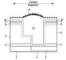
- FIGS. 1 to 5illustrate steps in the manufacturing of an interconnect structure.
- the structure 1comprises a first dielectric layer 2 formed of dielectric material, in this example ultra low K material. Which is adjacent to a first metal layer 3 , in this example copper.
- a thin barrier layer 4for example formed of conductive TiN, separates the dielectric layer 2 and the first metal layer 3 .
- An etch stop layer 5for example, formed from SiCN covers the first dielectric layer 2 and partly covers the first metal layer 3 .
- a second dielectric layer 6 comprising the ultra low K materialis formed on the etch stop layer 5 .
- the second dielectric layer 6contains a passage 7 having an open end 7 a and a closed end 7 b closed by the first metal layer 3 .
- the wall(s) 7 c of the passagedefine a first passage portion or trench 7 d having the open end 7 a and a second passage portion or via 7 e having the closed end 7 b .
- the first passage portion 7 dis wider than the second passage portion 7 e.
- a USG hard mask layer 8is formed on an upper surface of the second dielectric layer 6 .
- a TiN hard mask layeris 9 is formed on the USG hard mask layer 8 .
- the structure 1is fabricated using known standard techniques. Briefly, the low k layers are deposited with or without intermediate and top hard masks. Resists are spun and lithographically exposed. The resists are patterned, the hard masks etched and then the resists are removed. The porous low K material and the layer 5 are then etched to form the passageway 7 .
- a diffusion barrier layer 10is deposited over the walls of the passage 7 and the first metal layer 3 that closes the passage 7 .
- the barrier layer 10comprises TiN.
- the barrier layer 10is deposited using a halide based precursor, (a Ti halide precursor if the layer 9 is TiN) and preferably using ALD or CVD.
- halide species 11 from the precursorremain on the surface of the barrier layer 10 after the deposition of the barrier layer 10 is complete. These halide species serve to catalyse the subsequent deposition of a metal layer 12 , see FIG. 3 , in a preferred embodiment copper deposited using CVD.
- ALDis used to grow the barrier layer 10 .
- ALDutilises alternating pulses of two or more precursors separated from each other by a purge pulse consisting of an inert gas.
- a purge pulseconsisting of an inert gas.
- growthoccurs in a sub mono-layer by sub mono-layer fashion.
- the growthis self limiting because of occupancy of active sites. The consequences are threefold: 1) A very uniform and conformal growth behaviour is obtained, 2) The monolayer by sub monolayer growth behaviour allows full control over the total stack thickness just by setting the amount of cycles, 3) There are low in film contamination levels because reaction products are completely removed from the surface during each pulse sequence.
- Atomic Layer Deposition of TiNis carried out by using titanium iodide (TiI 4 ) and ammonia (NH 3 ) as precursors at a deposition temperature of 250-400° C.
- TiI 4titanium iodide
- NH 3ammonia
- the ALD techniqueis based on the principle that the gaseous reactants used in the CVD process are made to react with the wafer surface one at the time.
- the deposition sequence in the preferred embodimentis as follows. A suitable apparatus for performing the deposition is described in WO02/063677.
- one of the reactantsis introduced into a reaction chamber.
- This precursorreacts with the surface such that a chemical bonding with the substrate atoms takes place.
- the conditions in terms of temperature, pressure, etc.are selected such that only one monolayer or sub monolayer of new material is grown on the surface; condensation or decomposition of additional precursor material does not take place under the chosen conditions.
- the precursor flowis maintained long enough such that the chemisorbed monolayer is present everywhere on the surface, also in deep vias, around corners, etc.
- the chemisorbed monolayerresults in a new surface termination, characteristic for the specific precursor used.
- the surface termination of a silicon dioxide surfaceconsists of Si—OH groups. When this surface is exposed to TiI 4 vapour, Si—O—Ti(I) bonds will be formed and HI(g) will be released.
- an inert purge gasis introduced into the chamber that removes all gaseous precursor molecules (i.e. TiI 4 ) used in the first step.
- the purge gase.g. N 2 or Ar, is kept flowing sufficiently long to ensure a complete removal of the first type of precursor. As the monolayer grown in the first step is chemisorbed, the purge gas does not remove this layer.
- a second precursoris introduced into the chamber.
- the type of precursor, NH 3 in this exampleis selected such that it reacts with the monolayer grown in the first step to form an additional layer. This is done to avoid a pile up of halogens on the interface affecting adhesion and reliability performance. In the ALD TiN example, this leads to the formation of (gaseous) HI, while the surface now has a —O—Ti—NH 2 termination. Again, the reaction will proceed until all available iodide atoms on the —O—TiI 3 surface sites are replaced by —Ti—NH 2 groups. Also in this step, the flow of reactant gas is kept going long enough to ensure that all surface sites have reacted; at the same time, the conditions are such that no condensation takes place.
- the fourth stepis another purge with inert gas that removes all excess gas remaining from the third step.
- the first precursoris introduced again (i.e. TiI 4 ).
- This precursorreacts with the molecules chemisorbed in the third step, i.e. with the —Ti—NH 2 groups. This results in the formation of gaseous HI, and a surface terminated with —N—Ti(I) x groups.
- Each of the four basic stepsis repeated multiple times, until a TiN film with the desired thickness has been realized.
- metal halide precursorsand a Ti halide in particular
- metal halide precursorsand a Ti halide in particular
- a surface treatmentfor example, a plasma anneal to improve the interface and ensure complete removal of any halide.
- halideis allowed to remain at the surface of the barrier to catalyse the subsequent growth of metal layer, for example Copper.
- the copper layer 12is deposited using CVD with Cupraselect (RTM) Cu(hfac)(tmvs) a well known precursor widely used for depositing MOCVD copper films.
- RTMCupraselect
- Cu(hfac)(tmvs)a well known precursor widely used for depositing MOCVD copper films.
- iodinemay catalyse the growth of a Cu layer is described in detail in WO2003056612.
- This processincludes the step of depositing ethyl iodide to provide the catalyst.
- the catalystis residual halogen from a halogen pre-cursor used to deposit a first later of material.
- conformal filling of the copper layer 12arises because of the larger concentration of catalytic species on the bottom of the passage portions 7 d and 7 e when the Copper layer 12 starts to grow.
- the layer 12may be completed using electrochemical plating.
- remaining catalytic speciesmay be dispersed either in the electrochemical bath or in a simple rinse step.
- iodine based precursoran iodine based precursor
- different halide based precursorsmay be used in other embodiments of the invention.
- iodine based pre-cursorsare preferred over chlorine based pre-cursors for ALD TiN barrier deposition because a gaseous HCl by-product released during the TiCl 4 pulse, is able to etch underlying copper due to the formation of volatile CuCl gas. This may cause severe pitting on copper lines or films. The release of the CuCl gas may also cause the additional problem of the re-deposition of copper on the reactor walls and the incorporation of copper inside the TiN diffusion barrier degrading the barrier's diffusion.
- iodine based precursorsare also preferred over fluorinated precursors which may also be problematical. It is well known for example that the use of WF 6 is problematical when used in combination with oxide surfaces because of the etching of SiO 2 by HF. The use of WF 6 as a precursor for barrier layer deposition on low-k dielectrics would not be ideal since these materials have a high concentration of Si—O—Si bonds.
- halide precursorsthat do not form volatile by-products that react with other materials used in interconnect manufacturing.
- Iodine and bromine based pre-cursorsfor example, metal iodide and metal bromide based precursors comply with this requirement.
- an iodide precursoris preferred over a bromine precursor when a trench or via is to be filled with copper because iodine has an enhanced catalytic action to start a super-conformal copper fill process.
- Iodide based pre-cursorsare also preferred over chloride or fluoride based pre-cursors because iodine will float on copper during catalytic Cu DVD. Chloride or fluoride precursors are more likely to remain attached to the diffusion layer/copper interface and thus degrade yield and via resistance.
- a further advantage of using iodine pre-cursorsis their relative bulkiness which results in a limited precursor penetration inside porous low-k dielectrics.
Landscapes
- Engineering & Computer Science (AREA)
- General Physics & Mathematics (AREA)
- Physics & Mathematics (AREA)
- Condensed Matter Physics & Semiconductors (AREA)
- Manufacturing & Machinery (AREA)
- Computer Hardware Design (AREA)
- Microelectronics & Electronic Packaging (AREA)
- Power Engineering (AREA)
- General Chemical & Material Sciences (AREA)
- Chemical Kinetics & Catalysis (AREA)
- Chemical & Material Sciences (AREA)
- Internal Circuitry In Semiconductor Integrated Circuit Devices (AREA)
- Electrodes Of Semiconductors (AREA)
- Chemical Vapour Deposition (AREA)
Abstract
Description
- The present invention relates to a method of fabricating a structure, in particular but not exclusively, for a semiconductor device.
- The density of transistors on high performance integrated circuits (Ics) is steadily increasing. The integration of many active elements has necessitated that such ICs feature multiple layers of high density metal interconnects.
- Recently, the semiconductor industry has moved away from using aluminum interconnect metal with Silicon Dioxide dielectric between the metal lines, to using Copper metal and low-k dielectric materials.
- Copper reduces the resistance of the metal interconnect lines while low-k dielectrics reduce the parasitic capacitance between the metal lines. These new materials have been employed in a fabrication process called “Dual Damascene” which is used to create the multi-level, high density metal interconnections needed for advanced, high performance ICs.
- Atomic layer deposition (ALD) and chemical vapour deposition (CVD) are well known techniques which may be used to deposit conformal copper diffusion barriers and also copper seed layers in dual damascene type structures.
- A diffusion barrier is a protective layer deposited on the walls of a trench or via formed for example in a di-electric material, such as the low K materials mentioned above, and which prevents metal, for example copper, used to fill the trench or via during manufacture, diffusing into the di-electric material. A diffusion barrier may for example be formed of TiN.
- A metal seed layer is a layer of metal, for example copper, typically deposited over a diffusion barrier in a trench or via, which facilitates the subsequent complete filling of the trench or via with the metal.
- Embodiments of the present invention aim to provide a convenient method by which one layer may be grown upon another layer in a structure for a semiconductor device.
- According to the present invention there is provided a method of fabricating a structure for a semiconductor device, in which method, a halogen based pre-cursor is used during deposition of a first layer of material on a substrate and wherein residual halogen from the deposition is used to catalyse growth of a second layer of material on the first layer.
- In one embodiment, the first layer of material is a diffusion barrier layer deposited on the bottom and/or side walls of a trench or via defined in the substrate.
- The second layer of material may be a metallic layer which the residual halogen catalyses the growth of as the second layer fills the trench or via.
- Preferably, the halogen based precursor is iodine or bromine based.
- An embodiment of the invention will now be described by way of example only with reference to the accompanying drawings in which:
FIGS. 1 to 5 illustrate steps in the manufacturing of an interconnect structure.- Referring to
FIG. 1 of the accompanying drawings there is illustrated a part formeddamascene structure 1. Thestructure 1 comprises a firstdielectric layer 2 formed of dielectric material, in this example ultra low K material. Which is adjacent to afirst metal layer 3, in this example copper. Athin barrier layer 4, for example formed of conductive TiN, separates thedielectric layer 2 and thefirst metal layer 3. - An
etch stop layer 5, for example, formed from SiCN covers the firstdielectric layer 2 and partly covers thefirst metal layer 3. - A second
dielectric layer 6 comprising the ultra low K material is formed on theetch stop layer 5. The seconddielectric layer 6 contains apassage 7 having anopen end 7aand a closedend 7bclosed by thefirst metal layer 3. The wall(s)7cof the passage define a first passage portion ortrench 7dhaving theopen end 7aand a second passage portion or via7ehaving the closedend 7b. Thefirst passage portion 7dis wider than thesecond passage portion 7e. - A USG
hard mask layer 8 is formed on an upper surface of the seconddielectric layer 6. A TiN hard mask layer is9 is formed on the USGhard mask layer 8. - The
structure 1 is fabricated using known standard techniques. Briefly, the low k layers are deposited with or without intermediate and top hard masks. Resists are spun and lithographically exposed. The resists are patterned, the hard masks etched and then the resists are removed. The porous low K material and thelayer 5 are then etched to form thepassageway 7. - Referring now to
FIG. 2 , adiffusion barrier layer 10 is deposited over the walls of thepassage 7 and thefirst metal layer 3 that closes thepassage 7. In a preferred example thebarrier layer 10 comprises TiN. Thebarrier layer 10 is deposited using a halide based precursor, (a Ti halide precursor if thelayer 9 is TiN) and preferably using ALD or CVD. Advantageously,halide species 11 from the precursor remain on the surface of thebarrier layer 10 after the deposition of thebarrier layer 10 is complete. These halide species serve to catalyse the subsequent deposition of ametal layer 12, seeFIG. 3 , in a preferred embodiment copper deposited using CVD. - In a preferred embodiment, ALD is used to grow the
barrier layer 10. ALD utilises alternating pulses of two or more precursors separated from each other by a purge pulse consisting of an inert gas. By reactive adsorption to the surface, growth occurs in a sub mono-layer by sub mono-layer fashion. During each pulse the growth is self limiting because of occupancy of active sites. The consequences are threefold: 1) A very uniform and conformal growth behaviour is obtained, 2) The monolayer by sub monolayer growth behaviour allows full control over the total stack thickness just by setting the amount of cycles, 3) There are low in film contamination levels because reaction products are completely removed from the surface during each pulse sequence. - In a preferred embodiment of the present invention, Atomic Layer Deposition of TiN is carried out by using titanium iodide (TiI4) and ammonia (NH3) as precursors at a deposition temperature of 250-400° C. The ALD technique is based on the principle that the gaseous reactants used in the CVD process are made to react with the wafer surface one at the time. The deposition sequence in the preferred embodiment is as follows. A suitable apparatus for performing the deposition is described in WO02/063677.
- First, one of the reactants is introduced into a reaction chamber. This precursor reacts with the surface such that a chemical bonding with the substrate atoms takes place. The conditions in terms of temperature, pressure, etc. are selected such that only one monolayer or sub monolayer of new material is grown on the surface; condensation or decomposition of additional precursor material does not take place under the chosen conditions. The precursor flow is maintained long enough such that the chemisorbed monolayer is present everywhere on the surface, also in deep vias, around corners, etc. The chemisorbed monolayer results in a new surface termination, characteristic for the specific precursor used. E.g. the surface termination of a silicon dioxide surface consists of Si—OH groups. When this surface is exposed to TiI4vapour, Si—O—Ti(I) bonds will be formed and HI(g) will be released.
- Secondly. an inert purge gas is introduced into the chamber that removes all gaseous precursor molecules (i.e. TiI4) used in the first step. The purge gas, e.g. N2or Ar, is kept flowing sufficiently long to ensure a complete removal of the first type of precursor. As the monolayer grown in the first step is chemisorbed, the purge gas does not remove this layer.
- Thirdly, a second precursor is introduced into the chamber. The type of precursor, NH3in this example, is selected such that it reacts with the monolayer grown in the first step to form an additional layer. This is done to avoid a pile up of halogens on the interface affecting adhesion and reliability performance. In the ALD TiN example, this leads to the formation of (gaseous) HI, while the surface now has a —O—Ti—NH2termination. Again, the reaction will proceed until all available iodide atoms on the —O—TiI3surface sites are replaced by —Ti—NH2groups. Also in this step, the flow of reactant gas is kept going long enough to ensure that all surface sites have reacted; at the same time, the conditions are such that no condensation takes place.
- The fourth step is another purge with inert gas that removes all excess gas remaining from the third step.
- In the subsequent step, the first precursor is introduced again (i.e. TiI4). This precursor reacts with the molecules chemisorbed in the third step, i.e. with the —Ti—NH2groups. This results in the formation of gaseous HI, and a surface terminated with —N—Ti(I)xgroups.
- Each of the four basic steps is repeated multiple times, until a TiN film with the desired thickness has been realized.
- Although the use of metal halide precursors (and a Ti halide in particular) to grow layers in this way is known, it is normal practice to remove any halide remaining on the surface of the completed layer by application of a final NH3ALD half cycle. This is done to improve adhesion. Additionally, it is standard to apply further a surface treatment, for example, a plasma anneal to improve the interface and ensure complete removal of any halide.
- Contrary to this, in embodiments of the present invention, as mentioned above, halide is allowed to remain at the surface of the barrier to catalyse the subsequent growth of metal layer, for example Copper.
- In a preferred embodiment, the
copper layer 12 is deposited using CVD with Cupraselect (RTM) Cu(hfac)(tmvs) a well known precursor widely used for depositing MOCVD copper films. During the growth of thecopper layer 12,residual iodine ions 11 left from the step of depositing thebarrier layer 10, float to the top of thecopper layer 12 and do not get buried within the growing film. The presence of iodine catalyses the reduction of adsorbed Cu+ (hfac) molecule into copper giving rise to a growth rate that is larger than without using iodine. - A process by which iodine may catalyse the growth of a Cu layer is described in detail in WO2003056612. This process includes the step of depositing ethyl iodide to provide the catalyst. This is to be contrasted with embodiments of the invention in which the catalyst is residual halogen from a halogen pre-cursor used to deposit a first later of material.
- As illustrated in
FIG. 4 , conformal filling of thecopper layer 12 arises because of the larger concentration of catalytic species on the bottom of thepassage portions Copper layer 12 starts to grow. - After the deposition of a copper seed layer in this way, the
layer 12 may be completed using electrochemical plating. - As illustrated in
FIG. 5 , remaining catalytic species may be dispersed either in the electrochemical bath or in a simple rinse step. - Although in the preferred embodiment, an iodine based precursor is used, different halide based precursors may be used in other embodiments of the invention. However, iodine based pre-cursors are preferred over chlorine based pre-cursors for ALD TiN barrier deposition because a gaseous HCl by-product released during the TiCl4pulse, is able to etch underlying copper due to the formation of volatile CuCl gas. This may cause severe pitting on copper lines or films. The release of the CuCl gas may also cause the additional problem of the re-deposition of copper on the reactor walls and the incorporation of copper inside the TiN diffusion barrier degrading the barrier's diffusion.
- The use of iodine based precursors is also preferred over fluorinated precursors which may also be problematical. It is well known for example that the use of WF6is problematical when used in combination with oxide surfaces because of the etching of SiO2by HF. The use of WF6as a precursor for barrier layer deposition on low-k dielectrics would not be ideal since these materials have a high concentration of Si—O—Si bonds.
- Thus in embodiments involving the manufacture of a damascene structure it is preferable to use halide precursors that do not form volatile by-products that react with other materials used in interconnect manufacturing. Iodine and bromine based pre-cursors, for example, metal iodide and metal bromide based precursors comply with this requirement. In general, an iodide precursor is preferred over a bromine precursor when a trench or via is to be filled with copper because iodine has an enhanced catalytic action to start a super-conformal copper fill process.
- Iodide based pre-cursors are also preferred over chloride or fluoride based pre-cursors because iodine will float on copper during catalytic Cu DVD. Chloride or fluoride precursors are more likely to remain attached to the diffusion layer/copper interface and thus degrade yield and via resistance.
- A further advantage of using iodine pre-cursors is their relative bulkiness which results in a limited precursor penetration inside porous low-k dielectrics.
- Having thus described the present invention by reference to a preferred embodiment it is to be well understood that the embodiment in question is exemplary only and that modifications and variations such as will occur to those possessed of appropriate knowledge and skills may be made without departure from the spirit and scope of the invention as set forth in the appended claims and equivalents thereof. In the claims, any reference signs placed in parentheses shall not be construed as limiting the claims. The word “comprising” and “comprises”, and the like, does not exclude the presence of elements or steps other than those listed in any claim or the specification as a whole. The singular reference of an element does not exclude the plural reference of such elements.
- It will be apparent to a person skilled in the art that the various embodiments as described and/or claimed can be combined, without departing from the scope of the invention.
Claims (13)
Applications Claiming Priority (5)
| Application Number | Priority Date | Filing Date | Title |
|---|---|---|---|
| EP05300768.8 | 2005-09-23 | ||
| EP05300768 | 2005-09-23 | ||
| EP05300768 | 2005-09-23 | ||
| PCT/IB2006/053316WO2007034391A2 (en) | 2005-09-23 | 2006-09-15 | A method of fabricating a structure for a semiconductor device |
| IBPCT/IB2006/053316 | 2006-09-15 |
Publications (2)
| Publication Number | Publication Date |
|---|---|
| US20080299765A1true US20080299765A1 (en) | 2008-12-04 |
| US8349726B2 US8349726B2 (en) | 2013-01-08 |
Family
ID=37889213
Family Applications (1)
| Application Number | Title | Priority Date | Filing Date |
|---|---|---|---|
| US12/067,494Active2027-07-12US8349726B2 (en) | 2005-09-23 | 2006-09-15 | Method for fabricating a structure for a semiconductor device using a halogen based precursor |
Country Status (7)
| Country | Link |
|---|---|
| US (1) | US8349726B2 (en) |
| EP (1) | EP1949416A2 (en) |
| JP (1) | JP2009515319A (en) |
| KR (1) | KR20080047482A (en) |
| CN (1) | CN101438390A (en) |
| TW (1) | TW200739810A (en) |
| WO (1) | WO2007034391A2 (en) |
Cited By (5)
| Publication number | Priority date | Publication date | Assignee | Title |
|---|---|---|---|---|
| US8921821B2 (en)* | 2013-01-10 | 2014-12-30 | Micron Technology, Inc. | Memory cells |
| US9390909B2 (en) | 2013-11-07 | 2016-07-12 | Novellus Systems, Inc. | Soft landing nanolaminates for advanced patterning |
| US9478438B2 (en)* | 2014-08-20 | 2016-10-25 | Lam Research Corporation | Method and apparatus to deposit pure titanium thin film at low temperature using titanium tetraiodide precursor |
| US9478411B2 (en) | 2014-08-20 | 2016-10-25 | Lam Research Corporation | Method to tune TiOx stoichiometry using atomic layer deposited Ti film to minimize contact resistance for TiOx/Ti based MIS contact scheme for CMOS |
| TWI640040B (en)* | 2013-09-17 | 2018-11-01 | 應用材料股份有限公司 | Methods for stabilizing an interface post etch to minimize queue time issues before next processing step |
Families Citing this family (6)
| Publication number | Priority date | Publication date | Assignee | Title |
|---|---|---|---|---|
| US7951414B2 (en) | 2008-03-20 | 2011-05-31 | Micron Technology, Inc. | Methods of forming electrically conductive structures |
| US8618661B2 (en)* | 2011-10-03 | 2013-12-31 | Texas Instruments Incorporated | Die having coefficient of thermal expansion graded layer |
| US9859157B1 (en) | 2016-07-14 | 2018-01-02 | International Business Machines Corporation | Method for forming improved liner layer and semiconductor device including the same |
| JP6910118B2 (en)* | 2016-08-05 | 2021-07-28 | 東京エレクトロン株式会社 | Film formation method and film formation system, and surface treatment method |
| CN111162039A (en)* | 2018-11-08 | 2020-05-15 | 长鑫存储技术有限公司 | Metal conductive structure and preparation method of semiconductor device |
| US20240387379A1 (en)* | 2023-05-16 | 2024-11-21 | Taiwan Semiconductor Manufacturing Company, Ltd. | Method and apparatus for copper plating in semiconductor devices |
Citations (14)
| Publication number | Priority date | Publication date | Assignee | Title |
|---|---|---|---|---|
| US6468906B1 (en)* | 1998-12-28 | 2002-10-22 | Chartered Semiconductor Manufacturing Ltd. | Passivation of copper interconnect surfaces with a passivating metal layer |
| US20020173157A1 (en)* | 2001-03-29 | 2002-11-21 | Taiwan Semiconductor Manufacturing Co., Ltd. | Dual damascene method employing composite low dielectric constant dielectric layer having intrinsic etch stop characteristics |
| US20030001264A1 (en)* | 1997-12-09 | 2003-01-02 | Mehul Naik | Apparatus for integrating low dielectric constant materials into a multilevel metallization and interconnect structure |
| US20030176058A1 (en)* | 2002-03-18 | 2003-09-18 | Applies Materials, Inc. | Method of forming a dual damascene structure using an amorphous silicon hard mask |
| US20030180458A1 (en)* | 2002-01-17 | 2003-09-25 | Sundew Technologies, Llc | ALD apparatus and method |
| US20040000722A1 (en)* | 2002-06-28 | 2004-01-01 | James Powers | Semiconductor structure |
| US20040082164A1 (en)* | 2002-10-29 | 2004-04-29 | Taiwan Semiconductor Manufacturing Company | Chemistry for liner removal in a dual damascene process |
| US20040152300A1 (en)* | 2002-12-11 | 2004-08-05 | Kew Chan Shim | Method for forming metal wiring in a semiconductor device |
| US20050082606A1 (en)* | 2003-10-20 | 2005-04-21 | Stephan Grunow | Low K dielectric integrated circuit interconnect structure |
| US20050101123A1 (en)* | 2002-09-20 | 2005-05-12 | Mitsubishi Denki Kabushiki Kaisha | Via-filling material and process for fabricating semiconductor integrated circuit using the material |
| US20050153496A1 (en)* | 2004-01-12 | 2005-07-14 | Ngo Minh V. | Low stress sidewall spacer in integrated circuit technology |
| US20050277298A1 (en)* | 2003-07-11 | 2005-12-15 | Taiwan Semiconductor Manufacturing Company, Ltd. | Adhesion of copper and etch stop layer for copper alloy |
| US20060060956A1 (en)* | 2004-09-22 | 2006-03-23 | Tanikella Ravindra V | Materials, structures and methods for microelectronic packaging |
| US20060154493A1 (en)* | 2005-01-10 | 2006-07-13 | Reza Arghavani | Method for producing gate stack sidewall spacers |
Family Cites Families (2)
| Publication number | Priority date | Publication date | Assignee | Title |
|---|---|---|---|---|
| US6951804B2 (en) | 2001-02-02 | 2005-10-04 | Applied Materials, Inc. | Formation of a tantalum-nitride layer |
| KR100805843B1 (en) | 2001-12-28 | 2008-02-21 | 에이에스엠지니텍코리아 주식회사 | Copper wiring forming method, semiconductor device and copper wiring forming system manufactured accordingly |
- 2006
- 2006-09-15CNCNA2006800348422Apatent/CN101438390A/enactivePending
- 2006-09-15WOPCT/IB2006/053316patent/WO2007034391A2/enactiveApplication Filing
- 2006-09-15KRKR1020087009577Apatent/KR20080047482A/ennot_activeCeased
- 2006-09-15JPJP2008531844Apatent/JP2009515319A/ennot_activeWithdrawn
- 2006-09-15USUS12/067,494patent/US8349726B2/enactiveActive
- 2006-09-15EPEP06821091Apatent/EP1949416A2/ennot_activeWithdrawn
- 2006-09-20TWTW095134818Apatent/TW200739810A/enunknown
Patent Citations (14)
| Publication number | Priority date | Publication date | Assignee | Title |
|---|---|---|---|---|
| US20030001264A1 (en)* | 1997-12-09 | 2003-01-02 | Mehul Naik | Apparatus for integrating low dielectric constant materials into a multilevel metallization and interconnect structure |
| US6468906B1 (en)* | 1998-12-28 | 2002-10-22 | Chartered Semiconductor Manufacturing Ltd. | Passivation of copper interconnect surfaces with a passivating metal layer |
| US20020173157A1 (en)* | 2001-03-29 | 2002-11-21 | Taiwan Semiconductor Manufacturing Co., Ltd. | Dual damascene method employing composite low dielectric constant dielectric layer having intrinsic etch stop characteristics |
| US20030180458A1 (en)* | 2002-01-17 | 2003-09-25 | Sundew Technologies, Llc | ALD apparatus and method |
| US20030176058A1 (en)* | 2002-03-18 | 2003-09-18 | Applies Materials, Inc. | Method of forming a dual damascene structure using an amorphous silicon hard mask |
| US20040000722A1 (en)* | 2002-06-28 | 2004-01-01 | James Powers | Semiconductor structure |
| US20050101123A1 (en)* | 2002-09-20 | 2005-05-12 | Mitsubishi Denki Kabushiki Kaisha | Via-filling material and process for fabricating semiconductor integrated circuit using the material |
| US20040082164A1 (en)* | 2002-10-29 | 2004-04-29 | Taiwan Semiconductor Manufacturing Company | Chemistry for liner removal in a dual damascene process |
| US20040152300A1 (en)* | 2002-12-11 | 2004-08-05 | Kew Chan Shim | Method for forming metal wiring in a semiconductor device |
| US20050277298A1 (en)* | 2003-07-11 | 2005-12-15 | Taiwan Semiconductor Manufacturing Company, Ltd. | Adhesion of copper and etch stop layer for copper alloy |
| US20050082606A1 (en)* | 2003-10-20 | 2005-04-21 | Stephan Grunow | Low K dielectric integrated circuit interconnect structure |
| US20050153496A1 (en)* | 2004-01-12 | 2005-07-14 | Ngo Minh V. | Low stress sidewall spacer in integrated circuit technology |
| US20060060956A1 (en)* | 2004-09-22 | 2006-03-23 | Tanikella Ravindra V | Materials, structures and methods for microelectronic packaging |
| US20060154493A1 (en)* | 2005-01-10 | 2006-07-13 | Reza Arghavani | Method for producing gate stack sidewall spacers |
Cited By (10)
| Publication number | Priority date | Publication date | Assignee | Title |
|---|---|---|---|---|
| US8921821B2 (en)* | 2013-01-10 | 2014-12-30 | Micron Technology, Inc. | Memory cells |
| US9508931B2 (en) | 2013-01-10 | 2016-11-29 | Micron Technology, Inc. | Memory cells and methods of forming memory cells |
| US10388871B2 (en) | 2013-01-10 | 2019-08-20 | Micron Technology, Inc. | Memory cells and methods of forming memory cells |
| US10923658B2 (en) | 2013-01-10 | 2021-02-16 | Micron Technology, Inc. | Memory cells and methods of forming memory cells |
| TWI640040B (en)* | 2013-09-17 | 2018-11-01 | 應用材料股份有限公司 | Methods for stabilizing an interface post etch to minimize queue time issues before next processing step |
| US9390909B2 (en) | 2013-11-07 | 2016-07-12 | Novellus Systems, Inc. | Soft landing nanolaminates for advanced patterning |
| US9905423B2 (en) | 2013-11-07 | 2018-02-27 | Novellus Systems, Inc. | Soft landing nanolaminates for advanced patterning |
| US10192742B2 (en) | 2013-11-07 | 2019-01-29 | Novellus Systems, Inc. | Soft landing nanolaminates for advanced patterning |
| US9478438B2 (en)* | 2014-08-20 | 2016-10-25 | Lam Research Corporation | Method and apparatus to deposit pure titanium thin film at low temperature using titanium tetraiodide precursor |
| US9478411B2 (en) | 2014-08-20 | 2016-10-25 | Lam Research Corporation | Method to tune TiOx stoichiometry using atomic layer deposited Ti film to minimize contact resistance for TiOx/Ti based MIS contact scheme for CMOS |
Also Published As
| Publication number | Publication date |
|---|---|
| CN101438390A (en) | 2009-05-20 |
| TW200739810A (en) | 2007-10-16 |
| WO2007034391A3 (en) | 2008-12-04 |
| US8349726B2 (en) | 2013-01-08 |
| EP1949416A2 (en) | 2008-07-30 |
| KR20080047482A (en) | 2008-05-28 |
| WO2007034391A2 (en) | 2007-03-29 |
| JP2009515319A (en) | 2009-04-09 |
Similar Documents
| Publication | Publication Date | Title |
|---|---|---|
| US8349726B2 (en) | Method for fabricating a structure for a semiconductor device using a halogen based precursor | |
| TWI784036B (en) | Layer forming method | |
| TWI852426B (en) | Deposition method | |
| US7928006B2 (en) | Structure for a semiconductor device and a method of manufacturing the same | |
| JP5102416B2 (en) | Method for forming a thin film on a porous insulating layer in an integrated circuit and method for forming a metal nitride barrier layer on a porous insulating layer in an integrated circuit | |
| US6759325B2 (en) | Sealing porous structures | |
| JP3998830B2 (en) | Method of forming metal nitride film by chemical vapor deposition and method of forming metal contact of semiconductor device using the same | |
| US6727169B1 (en) | Method of making conformal lining layers for damascene metallization | |
| WO2001029891A1 (en) | Conformal lining layers for damascene metallization | |
| KR20020047126A (en) | Method for bottomless deposition of barrier layers in integrated circuit metallization schemes | |
| KR100519376B1 (en) | Method for Forming Barrier Layer of Semiconductor Device | |
| US7709376B2 (en) | Method for fabricating semiconductor device and semiconductor device | |
| EP1249865A2 (en) | Multi-layered barrier metal thin films for Cu interconnect by ALCVD | |
| TW202231914A (en) | Method of reducing titanium nitride etching during tungsten film formation | |
| KR100615602B1 (en) | Methods of forming a titanium nitride film having a smooth surface and methods of forming a semiconductor device using the same | |
| KR20230155949A (en) | Reduce line bending during metal filling process | |
| KR100551073B1 (en) | Thin Film Formation Method Using Pulsed Chemical Vapor Deposition | |
| KR19990029260A (en) | Method of forming metal nitride film by chemical vapor deposition and method of forming metal contact of semiconductor device using same | |
| US6812144B2 (en) | Method for forming metal wiring in a semiconductor device | |
| KR20250109721A (en) | Surface depassivation by thermal etching after nitrogen radical treatment |
Legal Events
| Date | Code | Title | Description |
|---|---|---|---|
| AS | Assignment | Owner name:NXP B.V., NETHERLANDS Free format text:ASSIGNMENT OF ASSIGNORS INTEREST;ASSIGNOR:BESLING, WIM;REEL/FRAME:020686/0739 Effective date:20080219 | |
| STCF | Information on status: patent grant | Free format text:PATENTED CASE | |
| AS | Assignment | Owner name:MORGAN STANLEY SENIOR FUNDING, INC., MARYLAND Free format text:SECURITY AGREEMENT SUPPLEMENT;ASSIGNOR:NXP B.V.;REEL/FRAME:038017/0058 Effective date:20160218 | |
| FPAY | Fee payment | Year of fee payment:4 | |
| AS | Assignment | Owner name:MORGAN STANLEY SENIOR FUNDING, INC., MARYLAND Free format text:CORRECTIVE ASSIGNMENT TO CORRECT THE REMOVE APPLICATION 12092129 PREVIOUSLY RECORDED ON REEL 038017 FRAME 0058. ASSIGNOR(S) HEREBY CONFIRMS THE SECURITY AGREEMENT SUPPLEMENT;ASSIGNOR:NXP B.V.;REEL/FRAME:039361/0212 Effective date:20160218 | |
| AS | Assignment | Owner name:MORGAN STANLEY SENIOR FUNDING, INC., MARYLAND Free format text:CORRECTIVE ASSIGNMENT TO CORRECT THE REMOVE APPLICATION 12681366 PREVIOUSLY RECORDED ON REEL 039361 FRAME 0212. ASSIGNOR(S) HEREBY CONFIRMS THE SECURITY AGREEMENT SUPPLEMENT;ASSIGNOR:NXP B.V.;REEL/FRAME:042762/0145 Effective date:20160218 Owner name:MORGAN STANLEY SENIOR FUNDING, INC., MARYLAND Free format text:CORRECTIVE ASSIGNMENT TO CORRECT THE REMOVE APPLICATION 12681366 PREVIOUSLY RECORDED ON REEL 038017 FRAME 0058. ASSIGNOR(S) HEREBY CONFIRMS THE SECURITY AGREEMENT SUPPLEMENT;ASSIGNOR:NXP B.V.;REEL/FRAME:042985/0001 Effective date:20160218 | |
| AS | Assignment | Owner name:NXP B.V., NETHERLANDS Free format text:RELEASE BY SECURED PARTY;ASSIGNOR:MORGAN STANLEY SENIOR FUNDING, INC.;REEL/FRAME:050745/0001 Effective date:20190903 | |
| AS | Assignment | Owner name:MORGAN STANLEY SENIOR FUNDING, INC., MARYLAND Free format text:CORRECTIVE ASSIGNMENT TO CORRECT THE REMOVE APPLICATION 12298143 PREVIOUSLY RECORDED ON REEL 042762 FRAME 0145. ASSIGNOR(S) HEREBY CONFIRMS THE SECURITY AGREEMENT SUPPLEMENT;ASSIGNOR:NXP B.V.;REEL/FRAME:051145/0184 Effective date:20160218 Owner name:MORGAN STANLEY SENIOR FUNDING, INC., MARYLAND Free format text:CORRECTIVE ASSIGNMENT TO CORRECT THE REMOVE APPLICATION 12298143 PREVIOUSLY RECORDED ON REEL 039361 FRAME 0212. ASSIGNOR(S) HEREBY CONFIRMS THE SECURITY AGREEMENT SUPPLEMENT;ASSIGNOR:NXP B.V.;REEL/FRAME:051029/0387 Effective date:20160218 Owner name:MORGAN STANLEY SENIOR FUNDING, INC., MARYLAND Free format text:CORRECTIVE ASSIGNMENT TO CORRECT THE REMOVE APPLICATION 12298143 PREVIOUSLY RECORDED ON REEL 042985 FRAME 0001. ASSIGNOR(S) HEREBY CONFIRMS THE SECURITY AGREEMENT SUPPLEMENT;ASSIGNOR:NXP B.V.;REEL/FRAME:051029/0001 Effective date:20160218 Owner name:MORGAN STANLEY SENIOR FUNDING, INC., MARYLAND Free format text:CORRECTIVE ASSIGNMENT TO CORRECT THE REMOVE APPLICATION12298143 PREVIOUSLY RECORDED ON REEL 039361 FRAME 0212. ASSIGNOR(S) HEREBY CONFIRMS THE SECURITY AGREEMENT SUPPLEMENT;ASSIGNOR:NXP B.V.;REEL/FRAME:051029/0387 Effective date:20160218 Owner name:MORGAN STANLEY SENIOR FUNDING, INC., MARYLAND Free format text:CORRECTIVE ASSIGNMENT TO CORRECT THE REMOVE APPLICATION12298143 PREVIOUSLY RECORDED ON REEL 042985 FRAME 0001. ASSIGNOR(S) HEREBY CONFIRMS THE SECURITY AGREEMENT SUPPLEMENT;ASSIGNOR:NXP B.V.;REEL/FRAME:051029/0001 Effective date:20160218 Owner name:MORGAN STANLEY SENIOR FUNDING, INC., MARYLAND Free format text:CORRECTIVE ASSIGNMENT TO CORRECT THE REMOVE APPLICATION 12298143 PREVIOUSLY RECORDED ON REEL 038017 FRAME 0058. ASSIGNOR(S) HEREBY CONFIRMS THE SECURITY AGREEMENT SUPPLEMENT;ASSIGNOR:NXP B.V.;REEL/FRAME:051030/0001 Effective date:20160218 Owner name:MORGAN STANLEY SENIOR FUNDING, INC., MARYLAND Free format text:CORRECTIVE ASSIGNMENT TO CORRECT THE REMOVE APPLICATION12298143 PREVIOUSLY RECORDED ON REEL 042762 FRAME 0145. ASSIGNOR(S) HEREBY CONFIRMS THE SECURITY AGREEMENT SUPPLEMENT;ASSIGNOR:NXP B.V.;REEL/FRAME:051145/0184 Effective date:20160218 | |
| MAFP | Maintenance fee payment | Free format text:PAYMENT OF MAINTENANCE FEE, 8TH YEAR, LARGE ENTITY (ORIGINAL EVENT CODE: M1552); ENTITY STATUS OF PATENT OWNER: LARGE ENTITY Year of fee payment:8 | |
| MAFP | Maintenance fee payment | Free format text:PAYMENT OF MAINTENANCE FEE, 12TH YEAR, LARGE ENTITY (ORIGINAL EVENT CODE: M1553); ENTITY STATUS OF PATENT OWNER: LARGE ENTITY Year of fee payment:12 |