US20080291730A1 - Reducing effects of program disturb in a memory device - Google Patents
Reducing effects of program disturb in a memory deviceDownload PDFInfo
- Publication number
- US20080291730A1 US20080291730A1US12/170,543US17054308AUS2008291730A1US 20080291730 A1US20080291730 A1US 20080291730A1US 17054308 AUS17054308 AUS 17054308AUS 2008291730 A1US2008291730 A1US 2008291730A1
- Authority
- US
- United States
- Prior art keywords
- memory cell
- cell bias
- program
- initial
- memory
- Prior art date
- Legal status (The legal status is an assumption and is not a legal conclusion. Google has not performed a legal analysis and makes no representation as to the accuracy of the status listed.)
- Granted
Links
- 230000001603reducing effectEffects0.000titleclaimsdescription3
- 230000007423decreaseEffects0.000claimsabstractdescription7
- 230000015654memoryEffects0.000claimsdescription128
- 238000000034methodMethods0.000claimsdescription23
- 230000003247decreasing effectEffects0.000claimsdescription12
- 230000004044responseEffects0.000claimsdescription12
- 230000001351cycling effectEffects0.000description7
- 238000004891communicationMethods0.000description3
- 238000010586diagramMethods0.000description3
- 230000000694effectsEffects0.000description3
- 230000006978adaptationEffects0.000description2
- 230000015556catabolic processEffects0.000description2
- 230000008878couplingEffects0.000description2
- 238000010168coupling processMethods0.000description2
- 238000005859coupling reactionMethods0.000description2
- 238000006731degradation reactionMethods0.000description2
- 239000011159matrix materialSubstances0.000description2
- 238000005457optimizationMethods0.000description2
- 230000003071parasitic effectEffects0.000description2
- 230000009467reductionEffects0.000description2
- 230000003213activating effectEffects0.000description1
- 230000008901benefitEffects0.000description1
- 239000003990capacitorSubstances0.000description1
- 230000001413cellular effectEffects0.000description1
- 230000006870functionEffects0.000description1
- PWPJGUXAGUPAHP-UHFFFAOYSA-NlufenuronChemical compoundC1=C(Cl)C(OC(F)(F)C(C(F)(F)F)F)=CC(Cl)=C1NC(=O)NC(=O)C1=C(F)C=CC=C1FPWPJGUXAGUPAHP-UHFFFAOYSA-N0.000description1
- 239000004065semiconductorSubstances0.000description1
- 239000007787solidSubstances0.000description1
- 239000000758substrateSubstances0.000description1
- 230000001360synchronised effectEffects0.000description1
Images


Classifications
- G—PHYSICS
- G11—INFORMATION STORAGE
- G11C—STATIC STORES
- G11C29/00—Checking stores for correct operation ; Subsequent repair; Testing stores during standby or offline operation
- G11C29/02—Detection or location of defective auxiliary circuits, e.g. defective refresh counters
- G—PHYSICS
- G11—INFORMATION STORAGE
- G11C—STATIC STORES
- G11C16/00—Erasable programmable read-only memories
- G11C16/02—Erasable programmable read-only memories electrically programmable
- G11C16/04—Erasable programmable read-only memories electrically programmable using variable threshold transistors, e.g. FAMOS
- G11C16/0483—Erasable programmable read-only memories electrically programmable using variable threshold transistors, e.g. FAMOS comprising cells having several storage transistors connected in series
- G—PHYSICS
- G11—INFORMATION STORAGE
- G11C—STATIC STORES
- G11C16/00—Erasable programmable read-only memories
- G11C16/02—Erasable programmable read-only memories electrically programmable
- G11C16/06—Auxiliary circuits, e.g. for writing into memory
- G11C16/34—Determination of programming status, e.g. threshold voltage, overprogramming or underprogramming, retention
- G11C16/3418—Disturbance prevention or evaluation; Refreshing of disturbed memory data
- G11C16/3427—Circuits or methods to prevent or reduce disturbance of the state of a memory cell when neighbouring cells are read or written
- G—PHYSICS
- G11—INFORMATION STORAGE
- G11C—STATIC STORES
- G11C16/00—Erasable programmable read-only memories
- G11C16/02—Erasable programmable read-only memories electrically programmable
- G11C16/06—Auxiliary circuits, e.g. for writing into memory
- G11C16/34—Determination of programming status, e.g. threshold voltage, overprogramming or underprogramming, retention
- G11C16/349—Arrangements for evaluating degradation, retention or wearout, e.g. by counting erase cycles
- G—PHYSICS
- G11—INFORMATION STORAGE
- G11C—STATIC STORES
- G11C29/00—Checking stores for correct operation ; Subsequent repair; Testing stores during standby or offline operation
- G11C29/02—Detection or location of defective auxiliary circuits, e.g. defective refresh counters
- G11C29/021—Detection or location of defective auxiliary circuits, e.g. defective refresh counters in voltage or current generators
- G—PHYSICS
- G11—INFORMATION STORAGE
- G11C—STATIC STORES
- G11C29/00—Checking stores for correct operation ; Subsequent repair; Testing stores during standby or offline operation
- G11C29/02—Detection or location of defective auxiliary circuits, e.g. defective refresh counters
- G11C29/028—Detection or location of defective auxiliary circuits, e.g. defective refresh counters with adaption or trimming of parameters
- G—PHYSICS
- G11—INFORMATION STORAGE
- G11C—STATIC STORES
- G11C16/00—Erasable programmable read-only memories
- G11C16/02—Erasable programmable read-only memories electrically programmable
- G11C16/04—Erasable programmable read-only memories electrically programmable using variable threshold transistors, e.g. FAMOS
Definitions
- the present inventionrelates generally to memory devices and in particular the present invention relates to non-volatile memory devices.
- RAMrandom-access memory
- ROMread only memory
- DRAMdynamic random access memory
- SDRAMsynchronous dynamic random access memory
- flash memoryflash memory
- Flash memory deviceshave developed into a popular source of non-volatile memory for a wide range of electronic applications. Flash memory devices typically use a one-transistor memory cell that allows for high memory densities, high reliability, and low power consumption. Common uses for flash memory include personal computers, personal digital assistants (PDAs), digital cameras, and cellular telephones. Program code and system data such as a basic input/output system (BIOS) are typically stored in flash memory devices for use in personal computer systems.
- BIOSbasic input/output system
- NANDflash memory array architecture
- NORNOR gate circuits
- the floating gate memory cells of the memory arrayare arranged in a matrix.
- the gates of each floating gate memory cell of the array matrixare connected by rows to word select lines (word lines) and their drains are connected to column bitlines.
- the source of each floating gate memory cellis typically connected to a common source line.
- the NOR architecture floating gate memory arrayis accessed by a row decoder activating a row of floating gate memory cells by selecting the word line connected to their gates.
- the row of selected memory cellsthen place their stored data values on the column bitlines by flowing a differing current if in a programmed state or not programmed state from the connected source line to the connected column bitlines.
- FIG. 1shows a portion of a typical prior art NAND flash memory array.
- the selected word line 100 for the flash memory cells being programmedis typically biased by programming pulses that start at a voltage of around 16V and may incrementally increase to more than 20V.
- the selected word line 100 of the cells 101 - 103 to be programmedis biased at 19V.
- the unselected word lines for the remaining cellsare biased at V pass . This is typically in an approximate range of 9-10V.
- the bit lines of the cells 101 - 103 to be programmedare biased at 0V while the inhibited bit lines are biased at V CC .
- parasitic capacitance coupling between the selected word line and adjacent word linesbecomes problematic. Because of the parasitic coupling, the neighboring cells are more prone to program disturb than the other cells that also share the common bit line with the cells being programmed. This causes the cells on neighboring word lines to experience program disturb.
- the program disturb conditionhas two operation modes: boosting mode and V pass mode.
- boosting modethe cell's channel is at a positive boosting voltage (e.g., 6V) with respect to the gate and the gate is at V pgm (e.g., 19V).
- V pass modethe cell's channel is at ground and the gate is at V pass (e.g., 10V).
- the cells 120 , 121 on the selected word line 100 and inhibited bit linesare influenced by boosting mode program disturb.
- the neighboring cells 110 - 118 that are coupled to the enabled bit linesexperience V pass mode program disturb.
- Program disturbis degraded as the number of program/erase cycles increase. As the quantity of program/erase cycles increase, the voltage difference between the programmed state and the erased state narrows. This makes the affected cells more susceptible to over-programming as the threshold voltage, V t , narrows. This is a result of the program disturb causing an increasing threshold voltage as the quantity of program/erase cycles increase.
- FIG. 1shows a typical prior art NAND architecture memory array with word line biasing.
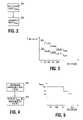
- FIG. 2shows a flowchart of one embodiment of a method of the present invention for adjusting V pass .
- FIG. 3shows a plot of last pulse voltage versus the quantity of program/erase cycles in accordance with the method of FIG. 2 .
- FIG. 4shows a flowchart of an alternate embodiment of a method of the present invention for adjusting V pass .
- FIG. 5shows a plot of V pass versus the quantity of program/erase cycles in accordance with the method of FIG. 4 .
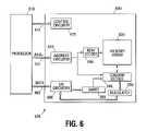
- FIG. 6shows a block diagram for one embodiment of a memory system of the present invention.
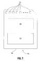
- FIG. 7shows a block diagram for one embodiment of a memory module of the present invention.
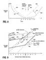
- FIG. 8shows a plot of failure rate of an arbitrary unit versus V pass voltage.
- FIG. 9shows a plot of failure rate versus partial page program cycle optimized at eight partial page cycles.
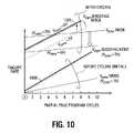
- FIG. 10shows a plot of failure rate versus partial page program cycle optimized at one partial page cycle.
- FIG. 8illustrates a plot of failure rate versus V pass voltage.
- the failure rateis for an arbitrary unit.
- This plotshows an initial V pgm boosting mode 801 with the failure rate decreasing as V pass increases until a predetermined optimized V pass is reached.
- the predetermined optimized V passis approximately 9.0V.
- An initial V pass mode 802 plotshows that as V pass increases from 9.0V, the failure rate of the arbitrary unit increases again.
- the V pass modehas degraded 811 considerably as compared with the V pgm boosting mode degradation 810 .
- the optimal V pass voltagehas also changed from the V pass 820 at the initial write/erase cycling of approximately 9.0V to approximately 8.0V after the 10 k write/erase cycles 821 .
- FIG. 9illustrates a plot of failure rate for an arbitrary unit versus partial page program cycle that is optimized at eight partial page cycles.
- This graphshows the plots for V pgm boosting before (initial) cycling 900 , V pass mode before cycling 902 , V pgm boosting mode after 10 k cycling 901 , and V pass mode after 10 k cycling 903 .
- V passneeds to be reduced as write/erase cycles increase.
- the lower bolded lines 900 , 902show the total failure rate before cycling and the upper bolded lines 901 , 903 show total failure rate after 10 k cycling. In this case, V pass is changed from 9V to 8V.
- FIG. 2illustrates a flowchart of one embodiment of a method for reducing the effects of program disturb by automatically adjusting V pass .
- This methodis comprised of first determining the last program voltage 201 , V pgm , that was able to successfully program memory cells.
- a non-volatile memory cellis programmed by a series of incrementally increasing voltage pulses on the selected word line.
- the pulsestypically start at an initial voltage (e.g., 16V) and increase by a set amount (e.g., 1V) until the desired cells are either programmed or an error occurs due to the cell or cells not being programmable.
- V passis based on the last V pgm voltage that successfully programmed the selected cell or cells. In an alternate embodiment, after an entire memory block has been programmed, V pass is based on the average V pgm that was used throughout the memory block to successfully program the cells. The voltage that biases the unselected word lines (i.e., V pass ) is then determined 203 in response to last or average V pgm just determined.
- V passtracks V pgm as a fixed ratio or percentage of V pgm .
- V passC*V pgm , where the constant C is approximately 0.5. Alternate embodiments can use other values for the constant C.
- FIG. 3illustrates a plot of the voltage of the last or average V pgm pulse versus the quantity of program/erase cycles. The plot shows that as the quantity of program/erase cycles increases, the voltage required to program the cells decreases. This is due to the build-up of electrons in the tunnel oxide between the substrate and the floating gate or trap layer. As the electrons in this layer increase over an increasing quantity of cycles, the voltage required on the gate to force the electrons to tunnel through the tunnel dielectric is reduced.
- V pass biasthat tracks V pgm as discussed previously is shown below the V pgm waveform. This shows V pass decreasing as 50% of V pgm .
- the values illustrated in FIG. 3are for purposes of illustration only. The voltage levels and the level of V pass as related to V pgm are not limited by the present invention.
- FIG. 4illustrates a flowchart of an alternate embodiment of a method of the present invention for programming memory cells in a flash memory array. This embodiment bases V pass on a count of program/erase cycle.
- V passis then updated in response to this count.
- V passstarts at 10V for a predetermined quantity of cycles (e.g., 1,000 cycles).
- V passis then reduced a predetermined voltage (e.g., 1V) for the next quantity of cycles (e.g., 7,000 cycles).
- V passis again reduced by the predetermined voltage after the next quantity of cycles.
- the voltages and program/erase cycles illustrated in FIG. 5are for purposes of illustration only.
- the present inventionis not limited to any one predetermined voltage reduction nor to any one quantity of cycles between V pass reductions.
- FIG. 6illustrates a functional block diagram of a memory device 600 that can incorporate the non-volatile memory cells of the present invention.
- the memory device 600is coupled to a processor 610 .
- the processor 610may be a microprocessor or some other type of controlling circuitry.
- the memory device 600 and the processor 610form part of an electronic system 620 .
- the memory device 600has been simplified to focus on features of the memory that are helpful in understanding the present invention.
- the memory deviceincludes an array of flash memory cells 630 or some other type of non-volatile memory cells.
- the memory array 630is arranged in banks of rows and columns.
- the control gates of each row of memory cellsis coupled with a word line while the drain and source connections of the memory cells are coupled to bit lines.
- bit linesAs is well known in the art, the connection of the cells to the bit lines depends on whether the array is a NAND architecture, a NOR architecture, an AND architecture, or some other array architecture.
- An address buffer circuit 640is provided to latch address signals provided on address input connections A 0 -Ax 642 . Address signals are received and decoded by a row decoder 644 and a column decoder 646 to access the memory array 630 . It will be appreciated by those skilled in the art, with the benefit of the present description, that the number of address input connections depends on the density and architecture of the memory array 630 . That is, the number of addresses increases with both increased memory cell counts and increased bank and block counts.
- the memory device 600reads data in the memory array 630 by sensing voltage or current changes in the memory array columns using sense amplifier/buffer circuitry 650 .
- the sense amplifier/buffer circuitryin one embodiment, is coupled to read and latch a row of data from the memory array 630 .
- Data input and output buffer circuitry 660is included for bi-directional data communication over a plurality of data connections 662 with the controller 610 .
- Write circuitry 655is provided to write data to the memory array.
- Control circuitry 670decodes signals provided on control connections 672 from the processor 610 . These signals are used to control the operations on the memory array 630 , including data read, data write, and erase operations.
- the control circuitry 670may be a state machine, a sequencer, or some other type of controller.
- the control circuitry 670 of the present inventionin one embodiment, is responsible for executing the method of the present invention for controlling the values of the selected word line programming voltage and the voltages on the unselected word lines.
- the flash memory device illustrated in FIG. 6has been simplified to facilitate a basic understanding of the features of the memory and is for purposes of illustration only. A more detailed understanding of internal circuitry and functions of flash memories are known to those skilled in the art. Alternate embodiments may include the flash memory cell of the present invention in other types of electronic systems.
- FIG. 7is an illustration of a memory module 700 that incorporates the memory cell embodiments as discussed previously.
- memory module 700is illustrated as a memory card, the concepts discussed with reference to memory module 700 are applicable to other types of removable or portable memory, e.g., USB flash drives.
- FIG. 7shows one example form factor, these concepts are applicable to other form factors as well.
- Memory module 700includes a housing 705 to enclose one or more memory devices 710 of the present invention.
- the housing 705includes one or more contacts 715 for communication with a host device.
- host devicesinclude digital cameras, digital recording and playback devices, PDAs, personal computers, memory card readers, interface hubs and the like.
- the contacts 715are in the form of a standardized interface.
- the contacts 715might be in the form of a USB Type-A male connector.
- the contacts 715are in the form of a semi-proprietary interface, such as might be found on COMPACTFLASH memory cards licensed by SANDISK Corporation, MEMORY STICK memory cards licensed by SONY Corporation, SD SECURE DIGITAL memory cards licensed by TOSHIBA Corporation and the like. In general, however, contacts 715 provide an interface for passing control, address and/or data signals between the memory module 700 and a host having compatible receptors for the contacts 715 .
- the memory module 700may optionally include additional circuitry 720 .
- the additional circuitry 720may include a memory controller for controlling access across multiple memory devices 710 and/or for providing a translation layer between an external host and a memory device 710 .
- a memory controllercould selectively couple an I/O connection (not shown in FIG. 7 ) of a memory device 710 to receive the appropriate signal at the appropriate I/O connection at the appropriate time or to provide the appropriate signal at the appropriate contact 715 at the appropriate time.
- the communication protocol between a host and the memory module 700may be different than what is required for access of a memory device 710 .
- a memory controllercould then translate the command sequences received from a host into the appropriate command sequences to achieve the desired access to the memory device 710 .
- Such translationmay further include changes in signal voltage levels in addition to command sequences.
- the additional circuitry 720may further include functionality unrelated to control of a memory device 710 .
- the additional circuitry 720may include circuitry to restrict read or write access to the memory module 700 , such as password protection, biometrics or the like.
- the additional circuitry 720may include circuitry to indicate a status of the memory module 700 .
- the additional circuitry 720may include functionality to determine whether power is being supplied to the memory module 700 and whether the memory module 700 is currently being accessed, and to display an indication of its status, such as a solid light while powered and a flashing light while being accessed.
- the additional circuitry 720may further include passive devices, such as decoupling capacitors to help regulate power requirements within the memory module 700 .
- the embodiments of the present inventionprovide a way to reduce or eliminate the over-programming of memory cells due to degradation of V pass disturb.
- V passcan be reduced as V pgm is reduced as program/erase cycles increase.
- V passcan be decreased based on a program/erase cycle count.
Landscapes
- Engineering & Computer Science (AREA)
- Microelectronics & Electronic Packaging (AREA)
- Read Only Memory (AREA)
Abstract
Description
- This Application is a Continuation of U.S. application Ser. No. 11/359,104, titled “MINIMIZING EFFECTS OF PROGRAM DISTURB IN A MEMORY DEVICE,” filed Feb. 22, 2006 (allowed), which is commonly assigned and incorporated herein by reference.
- The present invention relates generally to memory devices and in particular the present invention relates to non-volatile memory devices.
- Memory devices are typically provided as internal, semiconductor, integrated circuits in computers or other electronic devices. There are many different types of memory including random-access memory (RAM), read only memory (ROM), dynamic random access memory (DRAM), synchronous dynamic random access memory (SDRAM), and flash memory.
- Flash memory devices have developed into a popular source of non-volatile memory for a wide range of electronic applications. Flash memory devices typically use a one-transistor memory cell that allows for high memory densities, high reliability, and low power consumption. Common uses for flash memory include personal computers, personal digital assistants (PDAs), digital cameras, and cellular telephones. Program code and system data such as a basic input/output system (BIOS) are typically stored in flash memory devices for use in personal computer systems.
- Two common types of flash memory array architectures are the “NAND” and “NOR” architectures. These architectures are named for the resemblance that the basic memory cell configuration of each architecture has to a basic NAND or NOR gate circuits, respectively.
- In the NOR array architecture, the floating gate memory cells of the memory array are arranged in a matrix. The gates of each floating gate memory cell of the array matrix are connected by rows to word select lines (word lines) and their drains are connected to column bitlines. The source of each floating gate memory cell is typically connected to a common source line. The NOR architecture floating gate memory array is accessed by a row decoder activating a row of floating gate memory cells by selecting the word line connected to their gates. The row of selected memory cells then place their stored data values on the column bitlines by flowing a differing current if in a programmed state or not programmed state from the connected source line to the connected column bitlines.
FIG. 1 shows a portion of a typical prior art NAND flash memory array. Theselected word line 100 for the flash memory cells being programmed is typically biased by programming pulses that start at a voltage of around 16V and may incrementally increase to more than 20V. Theselected word line 100 of the cells101-103 to be programmed is biased at 19V. The unselected word lines for the remaining cells are biased at Vpass. This is typically in an approximate range of 9-10V. The bit lines of the cells101-103 to be programmed are biased at 0V while the inhibited bit lines are biased at VCC.- As NAND flash memory is scaled, parasitic capacitance coupling between the selected word line and adjacent word lines becomes problematic. Because of the parasitic coupling, the neighboring cells are more prone to program disturb than the other cells that also share the common bit line with the cells being programmed. This causes the cells on neighboring word lines to experience program disturb.
- The program disturb condition has two operation modes: boosting mode and Vpassmode. During the boosting mode, the cell's channel is at a positive boosting voltage (e.g., 6V) with respect to the gate and the gate is at Vpgm(e.g., 19V). During the Vpassmode, the cell's channel is at ground and the gate is at Vpass(e.g., 10V). In
FIG. 1 , thecells word line 100 and inhibited bit lines are influenced by boosting mode program disturb. The neighboring cells110-118 that are coupled to the enabled bit lines experience Vpassmode program disturb. - Program disturb is degraded as the number of program/erase cycles increase. As the quantity of program/erase cycles increase, the voltage difference between the programmed state and the erased state narrows. This makes the affected cells more susceptible to over-programming as the threshold voltage, Vt, narrows. This is a result of the program disturb causing an increasing threshold voltage as the quantity of program/erase cycles increase.
- For the reasons stated above, and for other reasons stated below which will become apparent to those skilled in the art upon reading and understanding the present specification, there is a need in the art for a way to minimize the effects of program disturb in a memory device.
FIG. 1 shows a typical prior art NAND architecture memory array with word line biasing.FIG. 2 shows a flowchart of one embodiment of a method of the present invention for adjusting Vpass.FIG. 3 shows a plot of last pulse voltage versus the quantity of program/erase cycles in accordance with the method ofFIG. 2 .FIG. 4 shows a flowchart of an alternate embodiment of a method of the present invention for adjusting Vpass.FIG. 5 shows a plot of Vpassversus the quantity of program/erase cycles in accordance with the method ofFIG. 4 .FIG. 6 shows a block diagram for one embodiment of a memory system of the present invention.FIG. 7 shows a block diagram for one embodiment of a memory module of the present invention.FIG. 8 shows a plot of failure rate of an arbitrary unit versus Vpassvoltage.FIG. 9 shows a plot of failure rate versus partial page program cycle optimized at eight partial page cycles.FIG. 10 shows a plot of failure rate versus partial page program cycle optimized at one partial page cycle.- In the following detailed description of the invention, reference is made to the accompanying drawings that form a part hereof and in which is shown, by way of illustration, specific embodiments in which the invention may be practiced. In the drawings, like numerals describe substantially similar components throughout the several views. These embodiments are described in sufficient detail to enable those skilled in the art to practice the invention. Other embodiments may be utilized and structural, logical, and electrical changes may be made without departing from the scope of the present invention. The following detailed description is, therefore, not to be taken in a limiting sense, and the scope of the present invention is defined only by the appended claims and equivalents thereof.
FIG. 8 illustrates a plot of failure rate versus Vpassvoltage. The failure rate is for an arbitrary unit.- This plot shows an initial Vpgmboosting mode801 with the failure rate decreasing as Vpassincreases until a predetermined optimized Vpassis reached. In the illustrated plot, the predetermined optimized Vpassis approximately 9.0V. An initial Vpassmode802 plot shows that as Vpassincreases from 9.0V, the failure rate of the arbitrary unit increases again.
- After 10 k write/erase cycles, the Vpassmode has degraded811 considerably as compared with the Vpgm
boosting mode degradation 810. The optimal Vpassvoltage has also changed from theV pass820 at the initial write/erase cycling of approximately 9.0V to approximately 8.0V after the 10 k write/erase cycles 821. FIG. 9 illustrates a plot of failure rate for an arbitrary unit versus partial page program cycle that is optimized at eight partial page cycles. This graph shows the plots for Vpgmboosting before (initial)cycling 900, Vpassmode before cycling902, Vpgmboosting mode after 10k cycling 901, and Vpassmode after 10k cycling 903. This shows that in order to decrease program disturb failure rate, Vpassneeds to be reduced as write/erase cycles increase. The lowerbolded lines bolded lines FIG. 10 illustrates a plot of failure rate for an arbitrary unit versus partial page program cycle that is optimized at one partial page cycle. This plot shows the Vpgmboosting mode (Vpass=7V) at one partial page program cycle optimization. Also shown is the Vpgmboosting mode (Vpass=6V) at one partial page program cycle optimization.FIG. 2 illustrates a flowchart of one embodiment of a method for reducing the effects of program disturb by automatically adjusting Vpass. This method is comprised of first determining thelast program voltage 201, Vpgm, that was able to successfully program memory cells.- As is well known in the art, a non-volatile memory cell is programmed by a series of incrementally increasing voltage pulses on the selected word line. The pulses typically start at an initial voltage (e.g., 16V) and increase by a set amount (e.g., 1V) until the desired cells are either programmed or an error occurs due to the cell or cells not being programmable.
- In one embodiment of the method of
FIG. 2 , Vpassis based on the last Vpgmvoltage that successfully programmed the selected cell or cells. In an alternate embodiment, after an entire memory block has been programmed, Vpassis based on the average Vpgmthat was used throughout the memory block to successfully program the cells. The voltage that biases the unselected word lines (i.e., Vpass) is then determined203 in response to last or average Vpgmjust determined. - In one embodiment, Vpasstracks Vpgmas a fixed ratio or percentage of Vpgm. For example, Vpass=C*Vpgm, where the constant C is approximately 0.5. Alternate embodiments can use other values for the constant C.
FIG. 3 illustrates a plot of the voltage of the last or average Vpgmpulse versus the quantity of program/erase cycles. The plot shows that as the quantity of program/erase cycles increases, the voltage required to program the cells decreases. This is due to the build-up of electrons in the tunnel oxide between the substrate and the floating gate or trap layer. As the electrons in this layer increase over an increasing quantity of cycles, the voltage required on the gate to force the electrons to tunnel through the tunnel dielectric is reduced.- The Vpassbias that tracks Vpgmas discussed previously is shown below the Vpgmwaveform. This shows Vpassdecreasing as 50% of Vpgm. The values illustrated in
FIG. 3 are for purposes of illustration only. The voltage levels and the level of Vpassas related to Vpgmare not limited by the present invention. FIG. 4 illustrates a flowchart of an alternate embodiment of a method of the present invention for programming memory cells in a flash memory array. This embodiment bases Vpasson a count of program/erase cycle.- Initially, the count of program/erase cycles is determined401. Vpassis then updated in response to this count. As the plot of
FIG. 5 shows, as the quantity of program/erase cycles increases, the voltage level of Vpassdecreases. In one embodiment, Vpassstarts at 10V for a predetermined quantity of cycles (e.g., 1,000 cycles). Vpassis then reduced a predetermined voltage (e.g., 1V) for the next quantity of cycles (e.g., 7,000 cycles). Vpassis again reduced by the predetermined voltage after the next quantity of cycles. - As in previous embodiments, the voltages and program/erase cycles illustrated in
FIG. 5 are for purposes of illustration only. The present invention is not limited to any one predetermined voltage reduction nor to any one quantity of cycles between Vpassreductions. FIG. 6 illustrates a functional block diagram of amemory device 600 that can incorporate the non-volatile memory cells of the present invention. Thememory device 600 is coupled to aprocessor 610. Theprocessor 610 may be a microprocessor or some other type of controlling circuitry. Thememory device 600 and theprocessor 610 form part of anelectronic system 620. Thememory device 600 has been simplified to focus on features of the memory that are helpful in understanding the present invention.- The memory device includes an array of
flash memory cells 630 or some other type of non-volatile memory cells. Thememory array 630 is arranged in banks of rows and columns. The control gates of each row of memory cells is coupled with a word line while the drain and source connections of the memory cells are coupled to bit lines. As is well known in the art, the connection of the cells to the bit lines depends on whether the array is a NAND architecture, a NOR architecture, an AND architecture, or some other array architecture. - An
address buffer circuit 640 is provided to latch address signals provided on address input connections A0-Ax 642. Address signals are received and decoded by arow decoder 644 and acolumn decoder 646 to access thememory array 630. It will be appreciated by those skilled in the art, with the benefit of the present description, that the number of address input connections depends on the density and architecture of thememory array 630. That is, the number of addresses increases with both increased memory cell counts and increased bank and block counts. - The
memory device 600 reads data in thememory array 630 by sensing voltage or current changes in the memory array columns using sense amplifier/buffer circuitry 650. The sense amplifier/buffer circuitry, in one embodiment, is coupled to read and latch a row of data from thememory array 630. Data input andoutput buffer circuitry 660 is included for bi-directional data communication over a plurality ofdata connections 662 with thecontroller 610. Writecircuitry 655 is provided to write data to the memory array. Control circuitry 670 decodes signals provided oncontrol connections 672 from theprocessor 610. These signals are used to control the operations on thememory array 630, including data read, data write, and erase operations. Thecontrol circuitry 670 may be a state machine, a sequencer, or some other type of controller. Thecontrol circuitry 670 of the present invention, in one embodiment, is responsible for executing the method of the present invention for controlling the values of the selected word line programming voltage and the voltages on the unselected word lines.- The flash memory device illustrated in
FIG. 6 has been simplified to facilitate a basic understanding of the features of the memory and is for purposes of illustration only. A more detailed understanding of internal circuitry and functions of flash memories are known to those skilled in the art. Alternate embodiments may include the flash memory cell of the present invention in other types of electronic systems. FIG. 7 is an illustration of amemory module 700 that incorporates the memory cell embodiments as discussed previously. Althoughmemory module 700 is illustrated as a memory card, the concepts discussed with reference tomemory module 700 are applicable to other types of removable or portable memory, e.g., USB flash drives. In addition, although one example form factor is depicted inFIG. 7 , these concepts are applicable to other form factors as well.Memory module 700 includes ahousing 705 to enclose one ormore memory devices 710 of the present invention. Thehousing 705 includes one ormore contacts 715 for communication with a host device. Examples of host devices include digital cameras, digital recording and playback devices, PDAs, personal computers, memory card readers, interface hubs and the like. For some embodiment, thecontacts 715 are in the form of a standardized interface. For example, with a USB flash drive, thecontacts 715 might be in the form of a USB Type-A male connector. For some embodiments, thecontacts 715 are in the form of a semi-proprietary interface, such as might be found on COMPACTFLASH memory cards licensed by SANDISK Corporation, MEMORY STICK memory cards licensed by SONY Corporation, SD SECURE DIGITAL memory cards licensed by TOSHIBA Corporation and the like. In general, however,contacts 715 provide an interface for passing control, address and/or data signals between thememory module 700 and a host having compatible receptors for thecontacts 715.- The
memory module 700 may optionally includeadditional circuitry 720. For some embodiments, theadditional circuitry 720 may include a memory controller for controlling access acrossmultiple memory devices 710 and/or for providing a translation layer between an external host and amemory device 710. For example, there may not be a one-to-one correspondence between the number ofcontacts 715 and a number of I/O connections to the one ormore memory devices 710. Thus, a memory controller could selectively couple an I/O connection (not shown inFIG. 7 ) of amemory device 710 to receive the appropriate signal at the appropriate I/O connection at the appropriate time or to provide the appropriate signal at theappropriate contact 715 at the appropriate time. Similarly, the communication protocol between a host and thememory module 700 may be different than what is required for access of amemory device 710. A memory controller could then translate the command sequences received from a host into the appropriate command sequences to achieve the desired access to thememory device 710. Such translation may further include changes in signal voltage levels in addition to command sequences. - The
additional circuitry 720 may further include functionality unrelated to control of amemory device 710. Theadditional circuitry 720 may include circuitry to restrict read or write access to thememory module 700, such as password protection, biometrics or the like. Theadditional circuitry 720 may include circuitry to indicate a status of thememory module 700. For example, theadditional circuitry 720 may include functionality to determine whether power is being supplied to thememory module 700 and whether thememory module 700 is currently being accessed, and to display an indication of its status, such as a solid light while powered and a flashing light while being accessed. Theadditional circuitry 720 may further include passive devices, such as decoupling capacitors to help regulate power requirements within thememory module 700. - In summary, the embodiments of the present invention provide a way to reduce or eliminate the over-programming of memory cells due to degradation of Vpassdisturb. By automatically adjusting the Vpassbias based on tracking the Vpgmvoltage, Vpasscan be reduced as Vpgmis reduced as program/erase cycles increase. Alternatively, Vpasscan be decreased based on a program/erase cycle count.
- Although specific embodiments have been illustrated and described herein, it will be appreciated by those of ordinary skill in the art that any arrangement that is calculated to achieve the same purpose may be substituted for the specific embodiments shown. Many adaptations of the invention will be apparent to those of ordinary skill in the art. Accordingly, this application is intended to cover any adaptations or variations of the invention. It is manifestly intended that this invention be limited only by the following claims and equivalents thereof.
Claims (19)
Priority Applications (2)
| Application Number | Priority Date | Filing Date | Title |
|---|---|---|---|
| US12/170,543US7715234B2 (en) | 2006-02-22 | 2008-07-10 | Reducing effects of program disturb in a memory device |
| US12/763,574US8023329B2 (en) | 2006-02-22 | 2010-04-20 | Reducing effects of program disturb in a memory device |
Applications Claiming Priority (2)
| Application Number | Priority Date | Filing Date | Title |
|---|---|---|---|
| US11/359,104US7408810B2 (en) | 2006-02-22 | 2006-02-22 | Minimizing effects of program disturb in a memory device |
| US12/170,543US7715234B2 (en) | 2006-02-22 | 2008-07-10 | Reducing effects of program disturb in a memory device |
Related Parent Applications (1)
| Application Number | Title | Priority Date | Filing Date |
|---|---|---|---|
| US11/359,104ContinuationUS7408810B2 (en) | 2006-02-22 | 2006-02-22 | Minimizing effects of program disturb in a memory device |
Related Child Applications (1)
| Application Number | Title | Priority Date | Filing Date |
|---|---|---|---|
| US12/763,574ContinuationUS8023329B2 (en) | 2006-02-22 | 2010-04-20 | Reducing effects of program disturb in a memory device |
Publications (2)
| Publication Number | Publication Date |
|---|---|
| US20080291730A1true US20080291730A1 (en) | 2008-11-27 |
| US7715234B2 US7715234B2 (en) | 2010-05-11 |
Family
ID=38428018
Family Applications (3)
| Application Number | Title | Priority Date | Filing Date |
|---|---|---|---|
| US11/359,104Active2026-11-11US7408810B2 (en) | 2006-02-22 | 2006-02-22 | Minimizing effects of program disturb in a memory device |
| US12/170,543ActiveUS7715234B2 (en) | 2006-02-22 | 2008-07-10 | Reducing effects of program disturb in a memory device |
| US12/763,574ActiveUS8023329B2 (en) | 2006-02-22 | 2010-04-20 | Reducing effects of program disturb in a memory device |
Family Applications Before (1)
| Application Number | Title | Priority Date | Filing Date |
|---|---|---|---|
| US11/359,104Active2026-11-11US7408810B2 (en) | 2006-02-22 | 2006-02-22 | Minimizing effects of program disturb in a memory device |
Family Applications After (1)
| Application Number | Title | Priority Date | Filing Date |
|---|---|---|---|
| US12/763,574ActiveUS8023329B2 (en) | 2006-02-22 | 2010-04-20 | Reducing effects of program disturb in a memory device |
Country Status (1)
| Country | Link |
|---|---|
| US (3) | US7408810B2 (en) |
Cited By (7)
| Publication number | Priority date | Publication date | Assignee | Title |
|---|---|---|---|---|
| US20100208523A1 (en)* | 2009-02-13 | 2010-08-19 | Micron Technology, Inc. | Dynamic soft program trims |
| US20100329010A1 (en)* | 2009-06-24 | 2010-12-30 | Yingda Dong | Read operation for memory with compensation for coupling based on write-erase cycles |
| US20110026331A1 (en)* | 2009-07-30 | 2011-02-03 | Yingda Dong | Program voltage compensation with word line bias change to suppress charge trapping in memory |
| US20120281487A1 (en)* | 2011-05-02 | 2012-11-08 | Manabu Sakaniwa | Semiconductor memory device and method of controlling the same |
| US8320185B2 (en) | 2010-03-31 | 2012-11-27 | Micron Technology, Inc. | Lifetime markers for memory devices |
| US9837167B2 (en) | 2015-08-24 | 2017-12-05 | Samsung Electronics Co., Ltd. | Method for operating storage device changing operation condition depending on data reliability |
| US10127984B2 (en) | 2015-08-24 | 2018-11-13 | Samsung Electronics Co., Ltd. | Method for operating storage device determining wordlines for writing user data depending on reuse period |
Families Citing this family (80)
| Publication number | Priority date | Publication date | Assignee | Title |
|---|---|---|---|---|
| US7408810B2 (en) | 2006-02-22 | 2008-08-05 | Micron Technology, Inc. | Minimizing effects of program disturb in a memory device |
| US7561469B2 (en)* | 2006-03-28 | 2009-07-14 | Micron Technology, Inc. | Programming method to reduce word line to word line breakdown for NAND flash |
| US7440321B2 (en)* | 2006-04-12 | 2008-10-21 | Micron Technology, Inc. | Multiple select gate architecture with select gates of different lengths |
| US7495966B2 (en) | 2006-05-01 | 2009-02-24 | Micron Technology, Inc. | Memory voltage cycle adjustment |
| WO2007132456A2 (en) | 2006-05-12 | 2007-11-22 | Anobit Technologies Ltd. | Memory device with adaptive capacity |
| WO2007132453A2 (en) | 2006-05-12 | 2007-11-22 | Anobit Technologies Ltd. | Distortion estimation and cancellation in memory devices |
| KR101202537B1 (en) | 2006-05-12 | 2012-11-19 | 애플 인크. | Combined distortion estimation and error correction coding for memory devices |
| US7471565B2 (en) | 2006-08-22 | 2008-12-30 | Micron Technology, Inc. | Reducing effects of program disturb in a memory device |
| WO2008026203A2 (en)* | 2006-08-27 | 2008-03-06 | Anobit Technologies | Estimation of non-linear distortion in memory devices |
| US7975192B2 (en) | 2006-10-30 | 2011-07-05 | Anobit Technologies Ltd. | Reading memory cells using multiple thresholds |
| WO2008068747A2 (en) | 2006-12-03 | 2008-06-12 | Anobit Technologies Ltd. | Automatic defect management in memory devices |
| US8151166B2 (en) | 2007-01-24 | 2012-04-03 | Anobit Technologies Ltd. | Reduction of back pattern dependency effects in memory devices |
| US8369141B2 (en) | 2007-03-12 | 2013-02-05 | Apple Inc. | Adaptive estimation of memory cell read thresholds |
| US8001320B2 (en) | 2007-04-22 | 2011-08-16 | Anobit Technologies Ltd. | Command interface for memory devices |
| US8234545B2 (en) | 2007-05-12 | 2012-07-31 | Apple Inc. | Data storage with incremental redundancy |
| WO2008139441A2 (en) | 2007-05-12 | 2008-11-20 | Anobit Technologies Ltd. | Memory device with internal signal processing unit |
| US8259497B2 (en) | 2007-08-06 | 2012-09-04 | Apple Inc. | Programming schemes for multi-level analog memory cells |
| US7885099B2 (en)* | 2007-09-18 | 2011-02-08 | Intel Corporation | Adaptive wordline programming bias of a phase change memory |
| US8174905B2 (en) | 2007-09-19 | 2012-05-08 | Anobit Technologies Ltd. | Programming orders for reducing distortion in arrays of multi-level analog memory cells |
| US8068360B2 (en) | 2007-10-19 | 2011-11-29 | Anobit Technologies Ltd. | Reading analog memory cells using built-in multi-threshold commands |
| US8527819B2 (en) | 2007-10-19 | 2013-09-03 | Apple Inc. | Data storage in analog memory cell arrays having erase failures |
| US8000141B1 (en) | 2007-10-19 | 2011-08-16 | Anobit Technologies Ltd. | Compensation for voltage drifts in analog memory cells |
| US8270246B2 (en) | 2007-11-13 | 2012-09-18 | Apple Inc. | Optimized selection of memory chips in multi-chips memory devices |
| US8225181B2 (en) | 2007-11-30 | 2012-07-17 | Apple Inc. | Efficient re-read operations from memory devices |
| US8209588B2 (en) | 2007-12-12 | 2012-06-26 | Anobit Technologies Ltd. | Efficient interference cancellation in analog memory cell arrays |
| US8085586B2 (en) | 2007-12-27 | 2011-12-27 | Anobit Technologies Ltd. | Wear level estimation in analog memory cells |
| US8156398B2 (en) | 2008-02-05 | 2012-04-10 | Anobit Technologies Ltd. | Parameter estimation based on error correction code parity check equations |
| US8230300B2 (en) | 2008-03-07 | 2012-07-24 | Apple Inc. | Efficient readout from analog memory cells using data compression |
| US7733705B2 (en)* | 2008-03-13 | 2010-06-08 | Micron Technology, Inc. | Reduction of punch-through disturb during programming of a memory device |
| US8400858B2 (en) | 2008-03-18 | 2013-03-19 | Apple Inc. | Memory device with reduced sense time readout |
| US8059457B2 (en) | 2008-03-18 | 2011-11-15 | Anobit Technologies Ltd. | Memory device with multiple-accuracy read commands |
| US8498151B1 (en) | 2008-08-05 | 2013-07-30 | Apple Inc. | Data storage in analog memory cells using modified pass voltages |
| US8949684B1 (en) | 2008-09-02 | 2015-02-03 | Apple Inc. | Segmented data storage |
| US8169825B1 (en) | 2008-09-02 | 2012-05-01 | Anobit Technologies Ltd. | Reliable data storage in analog memory cells subjected to long retention periods |
| US8482978B1 (en) | 2008-09-14 | 2013-07-09 | Apple Inc. | Estimation of memory cell read thresholds by sampling inside programming level distribution intervals |
| US8000135B1 (en) | 2008-09-14 | 2011-08-16 | Anobit Technologies Ltd. | Estimation of memory cell read thresholds by sampling inside programming level distribution intervals |
| US8239734B1 (en) | 2008-10-15 | 2012-08-07 | Apple Inc. | Efficient data storage in storage device arrays |
| US8713330B1 (en) | 2008-10-30 | 2014-04-29 | Apple Inc. | Data scrambling in memory devices |
| US8208304B2 (en) | 2008-11-16 | 2012-06-26 | Anobit Technologies Ltd. | Storage at M bits/cell density in N bits/cell analog memory cell devices, M>N |
| US8174857B1 (en) | 2008-12-31 | 2012-05-08 | Anobit Technologies Ltd. | Efficient readout schemes for analog memory cell devices using multiple read threshold sets |
| US8248831B2 (en) | 2008-12-31 | 2012-08-21 | Apple Inc. | Rejuvenation of analog memory cells |
| US8924661B1 (en) | 2009-01-18 | 2014-12-30 | Apple Inc. | Memory system including a controller and processors associated with memory devices |
| US8228701B2 (en) | 2009-03-01 | 2012-07-24 | Apple Inc. | Selective activation of programming schemes in analog memory cell arrays |
| US8259506B1 (en) | 2009-03-25 | 2012-09-04 | Apple Inc. | Database of memory read thresholds |
| US8832354B2 (en) | 2009-03-25 | 2014-09-09 | Apple Inc. | Use of host system resources by memory controller |
| US8238157B1 (en) | 2009-04-12 | 2012-08-07 | Apple Inc. | Selective re-programming of analog memory cells |
| US8479080B1 (en) | 2009-07-12 | 2013-07-02 | Apple Inc. | Adaptive over-provisioning in memory systems |
| US8495465B1 (en) | 2009-10-15 | 2013-07-23 | Apple Inc. | Error correction coding over multiple memory pages |
| US8677054B1 (en) | 2009-12-16 | 2014-03-18 | Apple Inc. | Memory management schemes for non-volatile memory devices |
| US8694814B1 (en) | 2010-01-10 | 2014-04-08 | Apple Inc. | Reuse of host hibernation storage space by memory controller |
| US8572311B1 (en) | 2010-01-11 | 2013-10-29 | Apple Inc. | Redundant data storage in multi-die memory systems |
| US9245653B2 (en) | 2010-03-15 | 2016-01-26 | Intelligent Intellectual Property Holdings 2 Llc | Reduced level cell mode for non-volatile memory |
| US8694853B1 (en) | 2010-05-04 | 2014-04-08 | Apple Inc. | Read commands for reading interfering memory cells |
| US8572423B1 (en) | 2010-06-22 | 2013-10-29 | Apple Inc. | Reducing peak current in memory systems |
| US8595591B1 (en) | 2010-07-11 | 2013-11-26 | Apple Inc. | Interference-aware assignment of programming levels in analog memory cells |
| US9104580B1 (en) | 2010-07-27 | 2015-08-11 | Apple Inc. | Cache memory for hybrid disk drives |
| US8645794B1 (en) | 2010-07-31 | 2014-02-04 | Apple Inc. | Data storage in analog memory cells using a non-integer number of bits per cell |
| US8856475B1 (en) | 2010-08-01 | 2014-10-07 | Apple Inc. | Efficient selection of memory blocks for compaction |
| US8694854B1 (en) | 2010-08-17 | 2014-04-08 | Apple Inc. | Read threshold setting based on soft readout statistics |
| US9021181B1 (en) | 2010-09-27 | 2015-04-28 | Apple Inc. | Memory management for unifying memory cell conditions by using maximum time intervals |
| US8456911B2 (en) | 2011-06-07 | 2013-06-04 | Sandisk Technologies Inc. | Intelligent shifting of read pass voltages for non-volatile storage |
| EP2549482B1 (en) | 2011-07-22 | 2018-05-23 | SanDisk Technologies LLC | Apparatus, system and method for determining a configuration parameter for solid-state storage media |
| JP2013058275A (en)* | 2011-09-07 | 2013-03-28 | Toshiba Corp | Semiconductor memory device |
| US20130159610A1 (en)* | 2011-12-16 | 2013-06-20 | Samsung Electronics Co., Ltd. | Non-volatile semiconductor memory device related method of operation |
| US8990644B2 (en) | 2011-12-22 | 2015-03-24 | Micron Technology, Inc. | Apparatus and methods of programming memory cells using adjustable charge state level(s) |
| US8576651B2 (en) | 2012-01-20 | 2013-11-05 | Sandisk 3D Llc | Temperature compensation of conductive bridge memory arrays |
| US8873316B2 (en) | 2012-07-25 | 2014-10-28 | Freescale Semiconductor, Inc. | Methods and systems for adjusting NVM cell bias conditions based upon operating temperature to reduce performance degradation |
| US8902667B2 (en)* | 2012-07-25 | 2014-12-02 | Freescale Semiconductor, Inc. | Methods and systems for adjusting NVM cell bias conditions for program/erase operations to reduce performance degradation |
| US9142315B2 (en) | 2012-07-25 | 2015-09-22 | Freescale Semiconductor, Inc. | Methods and systems for adjusting NVM cell bias conditions for read/verify operations to compensate for performance degradation |
| US9245637B2 (en)* | 2013-09-06 | 2016-01-26 | Sandisk Technologies Inc. | Systems and methods for read disturb management in non-volatile memory |
| US8988945B1 (en) | 2013-10-10 | 2015-03-24 | Sandisk Technologies Inc. | Programming time improvement for non-volatile memory |
| US9123424B2 (en) | 2013-12-17 | 2015-09-01 | Sandisk Technologies Inc. | Optimizing pass voltage and initial program voltage based on performance of non-volatile memory |
| US9324439B1 (en)* | 2014-10-20 | 2016-04-26 | Sandisk Technologies Inc. | Weak erase after programming to improve data retention in charge-trapping memory |
| KR102333746B1 (en) | 2015-09-02 | 2021-12-01 | 삼성전자주식회사 | Method for operating storage device managing wear level depending on reuse period |
| US11545221B2 (en) | 2018-06-29 | 2023-01-03 | Sandisk Technologies Llc | Concurrent programming of multiple cells for non-volatile memory devices |
| US10978156B2 (en) | 2018-06-29 | 2021-04-13 | Sandisk Technologies Llc | Concurrent programming of multiple cells for non-volatile memory devices |
| US11081170B2 (en) | 2018-12-19 | 2021-08-03 | Micron Technology, Inc. | Apparatus and methods for programming memory cells responsive to an indication of age of the memory cells |
| US11513879B2 (en) | 2019-02-20 | 2022-11-29 | Seagate Technologies Llc | Detection and mitigation for solid-state storage device read failures due to weak erase |
| US11556416B2 (en) | 2021-05-05 | 2023-01-17 | Apple Inc. | Controlling memory readout reliability and throughput by adjusting distance between read thresholds |
| US11847342B2 (en) | 2021-07-28 | 2023-12-19 | Apple Inc. | Efficient transfer of hard data and confidence levels in reading a nonvolatile memory |
Citations (71)
| Publication number | Priority date | Publication date | Assignee | Title |
|---|---|---|---|---|
| US5257225A (en)* | 1992-03-12 | 1993-10-26 | Micron Technology, Inc. | Method for programming programmable devices by utilizing single or multiple pulses varying in pulse width and amplitude |
| US5357463A (en)* | 1992-11-17 | 1994-10-18 | Micron Semiconductor, Inc. | Method for reverse programming of a flash EEPROM |
| US5424993A (en)* | 1993-11-15 | 1995-06-13 | Micron Technology, Inc. | Programming method for the selective healing of over-erased cells on a flash erasable programmable read-only memory device |
| US5511022A (en)* | 1988-12-15 | 1996-04-23 | Samsung Electronics Co., Ltd. | Depletion mode NAND string electrically erasable programmable semiconductor memory device and method for erasing and programming thereof |
| US5528547A (en)* | 1990-04-12 | 1996-06-18 | Kabushiki Kaisha Toshiba | Electrically erasable programmable read-only memory with electric field decreasing controller |
| US5621684A (en)* | 1995-03-31 | 1997-04-15 | Samsung Electronics Co., Ltd. | Nonvolatile semiconductor member with different pass potential applied to the first two adjacent word |
| US5677873A (en)* | 1995-09-19 | 1997-10-14 | Samsung Electronics Co., Ltd. | Methods of programming flash EEPROM integrated circuit memory devices to prevent inadvertent programming of nondesignated NAND memory cells therein |
| US5677875A (en)* | 1995-02-28 | 1997-10-14 | Nec Corporation | Non-volatile semiconductor memory device configured to minimize variations in threshold voltages of non-written memory cells and potentials of selected bit lines |
| US5680350A (en)* | 1994-12-14 | 1997-10-21 | Micron Technology, Inc. | Method for narrowing threshold voltage distribution in a block erased flash memory array |
| US5715194A (en)* | 1996-07-24 | 1998-02-03 | Advanced Micro Devices, Inc. | Bias scheme of program inhibit for random programming in a nand flash memory |
| US5768287A (en)* | 1996-10-24 | 1998-06-16 | Micron Quantum Devices, Inc. | Apparatus and method for programming multistate memory device |
| US5771346A (en)* | 1996-10-24 | 1998-06-23 | Micron Quantum Devices, Inc. | Apparatus and method for detecting over-programming condition in multistate memory device |
| US5907855A (en)* | 1996-10-15 | 1999-05-25 | Micron Technology, Inc. | Apparatus and method for reducing programming cycles for multistate memory system |
| US5917757A (en)* | 1996-08-01 | 1999-06-29 | Aplus Flash Technology, Inc. | Flash memory with high speed erasing structure using thin oxide semiconductor devices |
| US5920501A (en)* | 1997-12-12 | 1999-07-06 | Micron Technology, Inc. | Flash memory system and method for monitoring the disturb effect on memory cell blocks due to high voltage conditions of other memory cell blocks |
| US5930168A (en)* | 1998-03-20 | 1999-07-27 | Micron Technology, Inc. | Flash memory with adjustable write operation timing |
| US5959892A (en)* | 1997-08-26 | 1999-09-28 | Macronix International Co., Ltd. | Apparatus and method for programming virtual ground EPROM array cell without disturbing adjacent cells |
| US5991202A (en)* | 1998-09-24 | 1999-11-23 | Advanced Micro Devices, Inc. | Method for reducing program disturb during self-boosting in a NAND flash memory |
| US6061270A (en)* | 1997-12-31 | 2000-05-09 | Samsung Electronics Co., Ltd. | Method for programming a non-volatile memory device with program disturb control |
| US6107658A (en)* | 1997-02-27 | 2000-08-22 | Kabushiki Kaisha Toshiba | Non-volatile semiconductor memory device |
| US6157575A (en)* | 1998-03-26 | 2000-12-05 | Samsung Electronics Co., Ltd | Nonvolatile memory device and operating method thereof |
| US6163048A (en)* | 1995-10-25 | 2000-12-19 | Cypress Semiconductor Corporation | Semiconductor non-volatile memory device having a NAND cell structure |
| US6240023B1 (en)* | 1998-02-27 | 2001-05-29 | Micron Technology, Inc. | Method for efficiently executing soft programming of a memory block |
| US6240016B1 (en)* | 1999-12-17 | 2001-05-29 | Advanced Micro Devices, Inc. | Method to reduce read gate disturb for flash EEPROM application |
| US6370062B2 (en)* | 1999-12-10 | 2002-04-09 | Samsung Electronics Co., Ltd. | NAND-type flash memory device and method of operating the same |
| US6380033B1 (en)* | 1999-09-20 | 2002-04-30 | Advanced Micro Devices, Inc. | Process to improve read disturb for NAND flash memory devices |
| US20020060926A1 (en)* | 2000-11-22 | 2002-05-23 | Samsung Electronics Co., Ltd. | Flash memory device capable of preventing program disturb and method for programming the same |
| US20020075727A1 (en)* | 2000-12-14 | 2002-06-20 | Samsung Electronics Co., Ltd. | Non-volatile semiconductor memory device capable of preventing program disturb due to noise voltage induced at a string select line and program method thereof |
| US20020149958A1 (en)* | 2001-04-11 | 2002-10-17 | Mitsubishi Denki Kabushiki Kaisha | Non-volatile semiconductor memory |
| US6487117B1 (en)* | 1999-02-01 | 2002-11-26 | Samsung Electronics Co., Ltd. | Method for programming NAND-type flash memory device using bulk bias |
| US6493270B2 (en)* | 1999-07-01 | 2002-12-10 | Micron Technology, Inc. | Leakage detection in programming algorithm for a flash memory device |
| US6498752B1 (en)* | 2001-08-27 | 2002-12-24 | Aplus Flash Technology, Inc. | Three step write process used for a nonvolatile NOR type EEPROM memory |
| US6519181B2 (en)* | 2000-12-29 | 2003-02-11 | Hynix Semiconductor Inc. | Flash memory device |
| US6522584B1 (en)* | 2001-08-02 | 2003-02-18 | Micron Technology, Inc. | Programming methods for multi-level flash EEPROMs |
| US6620682B1 (en)* | 2001-02-27 | 2003-09-16 | Aplus Flash Technology, Inc. | Set of three level concurrent word line bias conditions for a nor type flash memory array |
| US6657915B2 (en)* | 2000-12-06 | 2003-12-02 | Samsung Electronics Co., Ltd. | Wordline driver for ensuring equal stress to wordlines in multi row address disturb test and method of driving the wordline driver |
| US6660585B1 (en)* | 2000-03-21 | 2003-12-09 | Aplus Flash Technology, Inc. | Stacked gate flash memory cell with reduced disturb conditions |
| US6661707B2 (en)* | 2001-02-16 | 2003-12-09 | Samsung Electronics Co., Ltd. | Method of programming NAND-type flash memory |
| US20040080980A1 (en)* | 2002-10-23 | 2004-04-29 | Chang-Hyun Lee | Methods of programming non-volatile semiconductor memory devices including coupling voltages and related devices |
| US6770714B2 (en)* | 2000-04-07 | 2004-08-03 | Borealis Technology Oy | Process for producing propylene based polymer compositions |
| US20040152262A1 (en)* | 2003-02-05 | 2004-08-05 | Kabushiki Kaisha Toshiba | Nonvolatile semiconductor memory, fabrication method for the same, semiconductor integrated circuits and systems |
| US6798694B2 (en)* | 2002-08-29 | 2004-09-28 | Micron Technology, Inc. | Method for reducing drain disturb in programming |
| US20040237000A1 (en)* | 2003-05-08 | 2004-11-25 | Micron Technology, Inc. | Program failure recovery |
| US20050088890A1 (en)* | 2002-11-29 | 2005-04-28 | Yasuhiko Matsunaga | NAND type flash EEPROM in which sequential programming process is performed by using different intermediate voltages |
| US6925011B2 (en)* | 2002-12-26 | 2005-08-02 | Micron Technology, Inc. | Programming flash memories |
| US20050226055A1 (en)* | 2004-04-13 | 2005-10-13 | Guterman Daniel C | Programming inhibit for non-volatile memory |
| US20050265097A1 (en)* | 1997-05-14 | 2005-12-01 | Kabushiki Kaisha Toshiba | Nonvolatile semiconductor memory device |
| US6975542B2 (en)* | 2003-05-08 | 2005-12-13 | Micron Technology, Inc. | NAND flash memory with improved read and verification threshold uniformity |
| US6977842B2 (en)* | 2003-09-16 | 2005-12-20 | Micron Technology, Inc. | Boosted substrate/tub programming for flash memories |
| US6982905B2 (en)* | 2003-10-09 | 2006-01-03 | Micron Technology, Inc. | Method and apparatus for reading NAND flash memory array |
| US20060002167A1 (en)* | 2004-06-30 | 2006-01-05 | Micron Technology, Inc. | Minimizing adjacent wordline disturb in a memory device |
| US20060023502A1 (en)* | 2002-09-24 | 2006-02-02 | Raul-Adrian Cernea | Non-volatile memory and method with reduced neighboring field errors |
| US7020017B2 (en)* | 2004-04-06 | 2006-03-28 | Sandisk Corporation | Variable programming of non-volatile memory |
| US7099193B2 (en)* | 2003-09-08 | 2006-08-29 | Kabushiki Kaisha Toshiba | Nonvolatile semiconductor memory device, electronic card and electronic apparatus |
| US7120059B2 (en)* | 2004-07-06 | 2006-10-10 | Macronix International Co., Ltd. | Memory array including multiple-gate charge trapping non-volatile cells |
| US20060274583A1 (en)* | 2005-06-03 | 2006-12-07 | Jeffrey Lutze | Starting program voltage shift with cycling of non-volatile memory |
| US7161833B2 (en)* | 2004-02-06 | 2007-01-09 | Sandisk Corporation | Self-boosting system for flash memory cells |
| US20070047314A1 (en)* | 2005-08-31 | 2007-03-01 | Micron Technology, Inc. | Programming method for NAND EEPROM |
| US7245534B2 (en)* | 2004-05-31 | 2007-07-17 | Kabushiki Kaisha Toshiba | Nonvolatile semiconductor memory |
| US20070177429A1 (en)* | 2006-01-24 | 2007-08-02 | Kabushiki Kaisha Toshiba | Nonvolatile semiconductor memory and nonvolatile memory system using thereof |
| US20070236992A1 (en)* | 2006-03-30 | 2007-10-11 | Ken Oowada | Self-boosting method with suppression of high lateral electric fields |
| US20070258286A1 (en)* | 2006-05-05 | 2007-11-08 | Masaaki Higashitani | Boosting methods for nand flash memory |
| US7355889B2 (en)* | 2005-12-19 | 2008-04-08 | Sandisk Corporation | Method for programming non-volatile memory with reduced program disturb using modified pass voltages |
| US20080101126A1 (en)* | 2006-10-30 | 2008-05-01 | Gerrit Jan Hemink | Faster programming of highest multi-level state for non-volatile memory |
| US7394693B2 (en)* | 2005-08-31 | 2008-07-01 | Micron Technology, Inc. | Multiple select gate architecture |
| US7408810B2 (en)* | 2006-02-22 | 2008-08-05 | Micron Technology, Inc. | Minimizing effects of program disturb in a memory device |
| US7440321B2 (en)* | 2006-04-12 | 2008-10-21 | Micron Technology, Inc. | Multiple select gate architecture with select gates of different lengths |
| US20080316827A1 (en)* | 2007-06-25 | 2008-12-25 | Masaaki Higashitani | Non-volatile storage with individually controllable shield plates between storage elements |
| US7471565B2 (en)* | 2006-08-22 | 2008-12-30 | Micron Technology, Inc. | Reducing effects of program disturb in a memory device |
| US20090018211A1 (en)* | 2007-07-09 | 2009-01-15 | Board Of Trustees Of Michigan State University | Method for inhibiting of COX2 and inflammation with phenolic aldehydes |
| US7561469B2 (en)* | 2006-03-28 | 2009-07-14 | Micron Technology, Inc. | Programming method to reduce word line to word line breakdown for NAND flash |
Family Cites Families (4)
| Publication number | Priority date | Publication date | Assignee | Title |
|---|---|---|---|---|
| JP3938309B2 (en) | 2002-01-22 | 2007-06-27 | 富士通株式会社 | Flash memory with reduced read disturb |
| CA2613617A1 (en)* | 2005-06-27 | 2007-01-04 | Daniel Drai | Compositions and methods for enhancement of sexual function |
| US20070047327A1 (en)* | 2005-08-31 | 2007-03-01 | Micron Technology, Inc. | Erase method for flash memory |
| US7736973B2 (en) | 2008-01-25 | 2010-06-15 | Sandisk Corporation | Non-volatile memory arrays having dual control gate cell structures and a thick control gate dielectric and methods of forming |
- 2006
- 2006-02-22USUS11/359,104patent/US7408810B2/enactiveActive
- 2008
- 2008-07-10USUS12/170,543patent/US7715234B2/enactiveActive
- 2010
- 2010-04-20USUS12/763,574patent/US8023329B2/enactiveActive
Patent Citations (76)
| Publication number | Priority date | Publication date | Assignee | Title |
|---|---|---|---|---|
| US5511022A (en)* | 1988-12-15 | 1996-04-23 | Samsung Electronics Co., Ltd. | Depletion mode NAND string electrically erasable programmable semiconductor memory device and method for erasing and programming thereof |
| US5528547A (en)* | 1990-04-12 | 1996-06-18 | Kabushiki Kaisha Toshiba | Electrically erasable programmable read-only memory with electric field decreasing controller |
| US5257225A (en)* | 1992-03-12 | 1993-10-26 | Micron Technology, Inc. | Method for programming programmable devices by utilizing single or multiple pulses varying in pulse width and amplitude |
| US5357463A (en)* | 1992-11-17 | 1994-10-18 | Micron Semiconductor, Inc. | Method for reverse programming of a flash EEPROM |
| US5424993A (en)* | 1993-11-15 | 1995-06-13 | Micron Technology, Inc. | Programming method for the selective healing of over-erased cells on a flash erasable programmable read-only memory device |
| US5680350A (en)* | 1994-12-14 | 1997-10-21 | Micron Technology, Inc. | Method for narrowing threshold voltage distribution in a block erased flash memory array |
| US5677875A (en)* | 1995-02-28 | 1997-10-14 | Nec Corporation | Non-volatile semiconductor memory device configured to minimize variations in threshold voltages of non-written memory cells and potentials of selected bit lines |
| US5621684A (en)* | 1995-03-31 | 1997-04-15 | Samsung Electronics Co., Ltd. | Nonvolatile semiconductor member with different pass potential applied to the first two adjacent word |
| US5677873A (en)* | 1995-09-19 | 1997-10-14 | Samsung Electronics Co., Ltd. | Methods of programming flash EEPROM integrated circuit memory devices to prevent inadvertent programming of nondesignated NAND memory cells therein |
| US6163048A (en)* | 1995-10-25 | 2000-12-19 | Cypress Semiconductor Corporation | Semiconductor non-volatile memory device having a NAND cell structure |
| US5715194A (en)* | 1996-07-24 | 1998-02-03 | Advanced Micro Devices, Inc. | Bias scheme of program inhibit for random programming in a nand flash memory |
| US5917757A (en)* | 1996-08-01 | 1999-06-29 | Aplus Flash Technology, Inc. | Flash memory with high speed erasing structure using thin oxide semiconductor devices |
| US5907855A (en)* | 1996-10-15 | 1999-05-25 | Micron Technology, Inc. | Apparatus and method for reducing programming cycles for multistate memory system |
| US5771346A (en)* | 1996-10-24 | 1998-06-23 | Micron Quantum Devices, Inc. | Apparatus and method for detecting over-programming condition in multistate memory device |
| US5768287A (en)* | 1996-10-24 | 1998-06-16 | Micron Quantum Devices, Inc. | Apparatus and method for programming multistate memory device |
| US6107658A (en)* | 1997-02-27 | 2000-08-22 | Kabushiki Kaisha Toshiba | Non-volatile semiconductor memory device |
| US20050265097A1 (en)* | 1997-05-14 | 2005-12-01 | Kabushiki Kaisha Toshiba | Nonvolatile semiconductor memory device |
| US5959892A (en)* | 1997-08-26 | 1999-09-28 | Macronix International Co., Ltd. | Apparatus and method for programming virtual ground EPROM array cell without disturbing adjacent cells |
| US5920501A (en)* | 1997-12-12 | 1999-07-06 | Micron Technology, Inc. | Flash memory system and method for monitoring the disturb effect on memory cell blocks due to high voltage conditions of other memory cell blocks |
| US6061270A (en)* | 1997-12-31 | 2000-05-09 | Samsung Electronics Co., Ltd. | Method for programming a non-volatile memory device with program disturb control |
| US6240023B1 (en)* | 1998-02-27 | 2001-05-29 | Micron Technology, Inc. | Method for efficiently executing soft programming of a memory block |
| US5930168A (en)* | 1998-03-20 | 1999-07-27 | Micron Technology, Inc. | Flash memory with adjustable write operation timing |
| US6157575A (en)* | 1998-03-26 | 2000-12-05 | Samsung Electronics Co., Ltd | Nonvolatile memory device and operating method thereof |
| US5991202A (en)* | 1998-09-24 | 1999-11-23 | Advanced Micro Devices, Inc. | Method for reducing program disturb during self-boosting in a NAND flash memory |
| US6487117B1 (en)* | 1999-02-01 | 2002-11-26 | Samsung Electronics Co., Ltd. | Method for programming NAND-type flash memory device using bulk bias |
| US6493270B2 (en)* | 1999-07-01 | 2002-12-10 | Micron Technology, Inc. | Leakage detection in programming algorithm for a flash memory device |
| US6380033B1 (en)* | 1999-09-20 | 2002-04-30 | Advanced Micro Devices, Inc. | Process to improve read disturb for NAND flash memory devices |
| US6370062B2 (en)* | 1999-12-10 | 2002-04-09 | Samsung Electronics Co., Ltd. | NAND-type flash memory device and method of operating the same |
| US6240016B1 (en)* | 1999-12-17 | 2001-05-29 | Advanced Micro Devices, Inc. | Method to reduce read gate disturb for flash EEPROM application |
| US6660585B1 (en)* | 2000-03-21 | 2003-12-09 | Aplus Flash Technology, Inc. | Stacked gate flash memory cell with reduced disturb conditions |
| US6770714B2 (en)* | 2000-04-07 | 2004-08-03 | Borealis Technology Oy | Process for producing propylene based polymer compositions |
| US6469933B2 (en)* | 2000-11-22 | 2002-10-22 | Samsung Electronics Co., Ltd. | Flash memory device capable of preventing program disturb and method for programming the same |
| US20020060926A1 (en)* | 2000-11-22 | 2002-05-23 | Samsung Electronics Co., Ltd. | Flash memory device capable of preventing program disturb and method for programming the same |
| US6657915B2 (en)* | 2000-12-06 | 2003-12-02 | Samsung Electronics Co., Ltd. | Wordline driver for ensuring equal stress to wordlines in multi row address disturb test and method of driving the wordline driver |
| US20020075727A1 (en)* | 2000-12-14 | 2002-06-20 | Samsung Electronics Co., Ltd. | Non-volatile semiconductor memory device capable of preventing program disturb due to noise voltage induced at a string select line and program method thereof |
| US6519181B2 (en)* | 2000-12-29 | 2003-02-11 | Hynix Semiconductor Inc. | Flash memory device |
| US6661707B2 (en)* | 2001-02-16 | 2003-12-09 | Samsung Electronics Co., Ltd. | Method of programming NAND-type flash memory |
| US6620682B1 (en)* | 2001-02-27 | 2003-09-16 | Aplus Flash Technology, Inc. | Set of three level concurrent word line bias conditions for a nor type flash memory array |
| US20020149958A1 (en)* | 2001-04-11 | 2002-10-17 | Mitsubishi Denki Kabushiki Kaisha | Non-volatile semiconductor memory |
| US6522584B1 (en)* | 2001-08-02 | 2003-02-18 | Micron Technology, Inc. | Programming methods for multi-level flash EEPROMs |
| US6498752B1 (en)* | 2001-08-27 | 2002-12-24 | Aplus Flash Technology, Inc. | Three step write process used for a nonvolatile NOR type EEPROM memory |
| US6798694B2 (en)* | 2002-08-29 | 2004-09-28 | Micron Technology, Inc. | Method for reducing drain disturb in programming |
| US20060023502A1 (en)* | 2002-09-24 | 2006-02-02 | Raul-Adrian Cernea | Non-volatile memory and method with reduced neighboring field errors |
| US20040080980A1 (en)* | 2002-10-23 | 2004-04-29 | Chang-Hyun Lee | Methods of programming non-volatile semiconductor memory devices including coupling voltages and related devices |
| US20050088890A1 (en)* | 2002-11-29 | 2005-04-28 | Yasuhiko Matsunaga | NAND type flash EEPROM in which sequential programming process is performed by using different intermediate voltages |
| US6925011B2 (en)* | 2002-12-26 | 2005-08-02 | Micron Technology, Inc. | Programming flash memories |
| US20040152262A1 (en)* | 2003-02-05 | 2004-08-05 | Kabushiki Kaisha Toshiba | Nonvolatile semiconductor memory, fabrication method for the same, semiconductor integrated circuits and systems |
| US20040237000A1 (en)* | 2003-05-08 | 2004-11-25 | Micron Technology, Inc. | Program failure recovery |
| US6975542B2 (en)* | 2003-05-08 | 2005-12-13 | Micron Technology, Inc. | NAND flash memory with improved read and verification threshold uniformity |
| US7099193B2 (en)* | 2003-09-08 | 2006-08-29 | Kabushiki Kaisha Toshiba | Nonvolatile semiconductor memory device, electronic card and electronic apparatus |
| US6977842B2 (en)* | 2003-09-16 | 2005-12-20 | Micron Technology, Inc. | Boosted substrate/tub programming for flash memories |
| US6982905B2 (en)* | 2003-10-09 | 2006-01-03 | Micron Technology, Inc. | Method and apparatus for reading NAND flash memory array |
| US7161833B2 (en)* | 2004-02-06 | 2007-01-09 | Sandisk Corporation | Self-boosting system for flash memory cells |
| US7020017B2 (en)* | 2004-04-06 | 2006-03-28 | Sandisk Corporation | Variable programming of non-volatile memory |
| US20050226055A1 (en)* | 2004-04-13 | 2005-10-13 | Guterman Daniel C | Programming inhibit for non-volatile memory |
| US7245534B2 (en)* | 2004-05-31 | 2007-07-17 | Kabushiki Kaisha Toshiba | Nonvolatile semiconductor memory |
| US20060002167A1 (en)* | 2004-06-30 | 2006-01-05 | Micron Technology, Inc. | Minimizing adjacent wordline disturb in a memory device |
| US7212435B2 (en)* | 2004-06-30 | 2007-05-01 | Micron Technology, Inc. | Minimizing adjacent wordline disturb in a memory device |
| US7120059B2 (en)* | 2004-07-06 | 2006-10-10 | Macronix International Co., Ltd. | Memory array including multiple-gate charge trapping non-volatile cells |
| US20060274583A1 (en)* | 2005-06-03 | 2006-12-07 | Jeffrey Lutze | Starting program voltage shift with cycling of non-volatile memory |
| US7394693B2 (en)* | 2005-08-31 | 2008-07-01 | Micron Technology, Inc. | Multiple select gate architecture |
| US7499330B2 (en)* | 2005-08-31 | 2009-03-03 | Micron Technology, Inc. | Programming method for NAND EEPROM |
| US7292476B2 (en)* | 2005-08-31 | 2007-11-06 | Micron Technology, Inc. | Programming method for NAND EEPROM |
| US20080253187A1 (en)* | 2005-08-31 | 2008-10-16 | Micron Technology, Inc. | Multiple select gate architecture |
| US20070047314A1 (en)* | 2005-08-31 | 2007-03-01 | Micron Technology, Inc. | Programming method for NAND EEPROM |
| US7355889B2 (en)* | 2005-12-19 | 2008-04-08 | Sandisk Corporation | Method for programming non-volatile memory with reduced program disturb using modified pass voltages |
| US20070177429A1 (en)* | 2006-01-24 | 2007-08-02 | Kabushiki Kaisha Toshiba | Nonvolatile semiconductor memory and nonvolatile memory system using thereof |
| US7408810B2 (en)* | 2006-02-22 | 2008-08-05 | Micron Technology, Inc. | Minimizing effects of program disturb in a memory device |
| US7561469B2 (en)* | 2006-03-28 | 2009-07-14 | Micron Technology, Inc. | Programming method to reduce word line to word line breakdown for NAND flash |
| US20070236992A1 (en)* | 2006-03-30 | 2007-10-11 | Ken Oowada | Self-boosting method with suppression of high lateral electric fields |
| US7440321B2 (en)* | 2006-04-12 | 2008-10-21 | Micron Technology, Inc. | Multiple select gate architecture with select gates of different lengths |
| US20070258286A1 (en)* | 2006-05-05 | 2007-11-08 | Masaaki Higashitani | Boosting methods for nand flash memory |
| US7471565B2 (en)* | 2006-08-22 | 2008-12-30 | Micron Technology, Inc. | Reducing effects of program disturb in a memory device |
| US20080101126A1 (en)* | 2006-10-30 | 2008-05-01 | Gerrit Jan Hemink | Faster programming of highest multi-level state for non-volatile memory |
| US20080316827A1 (en)* | 2007-06-25 | 2008-12-25 | Masaaki Higashitani | Non-volatile storage with individually controllable shield plates between storage elements |
| US20090018211A1 (en)* | 2007-07-09 | 2009-01-15 | Board Of Trustees Of Michigan State University | Method for inhibiting of COX2 and inflammation with phenolic aldehydes |
Cited By (13)
| Publication number | Priority date | Publication date | Assignee | Title |
|---|---|---|---|---|
| US20100208523A1 (en)* | 2009-02-13 | 2010-08-19 | Micron Technology, Inc. | Dynamic soft program trims |
| US8199585B2 (en) | 2009-02-13 | 2012-06-12 | Micron Technology, Inc. | Dynamic soft program trims |
| US7920427B2 (en) | 2009-02-13 | 2011-04-05 | Micron Technology, Inc. | Dynamic soft program trims |
| US20110182122A1 (en)* | 2009-02-13 | 2011-07-28 | Micron Technology, Inc. | Dynamic soft program trims |
| US20100329010A1 (en)* | 2009-06-24 | 2010-12-30 | Yingda Dong | Read operation for memory with compensation for coupling based on write-erase cycles |
| US7898864B2 (en) | 2009-06-24 | 2011-03-01 | Sandisk Corporation | Read operation for memory with compensation for coupling based on write-erase cycles |
| US7995394B2 (en) | 2009-07-30 | 2011-08-09 | Sandisk Technologies Inc. | Program voltage compensation with word line bias change to suppress charge trapping in memory |
| US20110026331A1 (en)* | 2009-07-30 | 2011-02-03 | Yingda Dong | Program voltage compensation with word line bias change to suppress charge trapping in memory |
| US8320185B2 (en) | 2010-03-31 | 2012-11-27 | Micron Technology, Inc. | Lifetime markers for memory devices |
| US8854892B2 (en) | 2010-03-31 | 2014-10-07 | Micron Technology, Inc. | Lifetime markers for memory devices |
| US20120281487A1 (en)* | 2011-05-02 | 2012-11-08 | Manabu Sakaniwa | Semiconductor memory device and method of controlling the same |
| US9837167B2 (en) | 2015-08-24 | 2017-12-05 | Samsung Electronics Co., Ltd. | Method for operating storage device changing operation condition depending on data reliability |
| US10127984B2 (en) | 2015-08-24 | 2018-11-13 | Samsung Electronics Co., Ltd. | Method for operating storage device determining wordlines for writing user data depending on reuse period |
Also Published As
| Publication number | Publication date |
|---|---|
| US20100202210A1 (en) | 2010-08-12 |
| US7408810B2 (en) | 2008-08-05 |
| US8023329B2 (en) | 2011-09-20 |
| US7715234B2 (en) | 2010-05-11 |
| US20070195603A1 (en) | 2007-08-23 |
Similar Documents
| Publication | Publication Date | Title |
|---|---|---|
| US7715234B2 (en) | Reducing effects of program disturb in a memory device | |
| US8159879B2 (en) | Reducing effects of program disturb in a memory device | |
| US8891309B2 (en) | Reducing read failure in a memory device | |
| US8462548B2 (en) | Non-volatile memory device capable of reducing floating gate-to-floating gate coupling effect during programming | |
| US7733699B2 (en) | Mimicking program verify drain resistance in a memory device | |
| US8144519B2 (en) | Programming a flash memory device | |
| KR101117413B1 (en) | Non-volatile multilevel memory cell programming with more than two verify voltages per level | |
| US8179721B2 (en) | Non-volatile memory device with both single and multiple level cells | |
| US8072814B2 (en) | NAND with back biased operation | |
| US7483311B2 (en) | Erase operation in a flash memory device | |
| WO2009046171A1 (en) | Reducing effects of program disturb in a memory device | |
| KR20060119988A (en) | No erase of nonvolatile memory | |
| US7663930B2 (en) | Programming a non-volatile memory device |
Legal Events
| Date | Code | Title | Description |
|---|---|---|---|
| FEPP | Fee payment procedure | Free format text:PAYOR NUMBER ASSIGNED (ORIGINAL EVENT CODE: ASPN); ENTITY STATUS OF PATENT OWNER: LARGE ENTITY | |
| STCF | Information on status: patent grant | Free format text:PATENTED CASE | |
| FPAY | Fee payment | Year of fee payment:4 | |
| AS | Assignment | Owner name:U.S. BANK NATIONAL ASSOCIATION, AS COLLATERAL AGENT, CALIFORNIA Free format text:SECURITY INTEREST;ASSIGNOR:MICRON TECHNOLOGY, INC.;REEL/FRAME:038669/0001 Effective date:20160426 Owner name:U.S. BANK NATIONAL ASSOCIATION, AS COLLATERAL AGEN Free format text:SECURITY INTEREST;ASSIGNOR:MICRON TECHNOLOGY, INC.;REEL/FRAME:038669/0001 Effective date:20160426 | |
| AS | Assignment | Owner name:MORGAN STANLEY SENIOR FUNDING, INC., AS COLLATERAL AGENT, MARYLAND Free format text:PATENT SECURITY AGREEMENT;ASSIGNOR:MICRON TECHNOLOGY, INC.;REEL/FRAME:038954/0001 Effective date:20160426 Owner name:MORGAN STANLEY SENIOR FUNDING, INC., AS COLLATERAL Free format text:PATENT SECURITY AGREEMENT;ASSIGNOR:MICRON TECHNOLOGY, INC.;REEL/FRAME:038954/0001 Effective date:20160426 | |
| AS | Assignment | Owner name:U.S. BANK NATIONAL ASSOCIATION, AS COLLATERAL AGENT, CALIFORNIA Free format text:CORRECTIVE ASSIGNMENT TO CORRECT THE REPLACE ERRONEOUSLY FILED PATENT #7358718 WITH THE CORRECT PATENT #7358178 PREVIOUSLY RECORDED ON REEL 038669 FRAME 0001. ASSIGNOR(S) HEREBY CONFIRMS THE SECURITY INTEREST;ASSIGNOR:MICRON TECHNOLOGY, INC.;REEL/FRAME:043079/0001 Effective date:20160426 Owner name:U.S. BANK NATIONAL ASSOCIATION, AS COLLATERAL AGEN Free format text:CORRECTIVE ASSIGNMENT TO CORRECT THE REPLACE ERRONEOUSLY FILED PATENT #7358718 WITH THE CORRECT PATENT #7358178 PREVIOUSLY RECORDED ON REEL 038669 FRAME 0001. ASSIGNOR(S) HEREBY CONFIRMS THE SECURITY INTEREST;ASSIGNOR:MICRON TECHNOLOGY, INC.;REEL/FRAME:043079/0001 Effective date:20160426 | |
| MAFP | Maintenance fee payment | Free format text:PAYMENT OF MAINTENANCE FEE, 8TH YEAR, LARGE ENTITY (ORIGINAL EVENT CODE: M1552) Year of fee payment:8 | |
| AS | Assignment | Owner name:JPMORGAN CHASE BANK, N.A., AS COLLATERAL AGENT, ILLINOIS Free format text:SECURITY INTEREST;ASSIGNORS:MICRON TECHNOLOGY, INC.;MICRON SEMICONDUCTOR PRODUCTS, INC.;REEL/FRAME:047540/0001 Effective date:20180703 Owner name:JPMORGAN CHASE BANK, N.A., AS COLLATERAL AGENT, IL Free format text:SECURITY INTEREST;ASSIGNORS:MICRON TECHNOLOGY, INC.;MICRON SEMICONDUCTOR PRODUCTS, INC.;REEL/FRAME:047540/0001 Effective date:20180703 | |
| AS | Assignment | Owner name:MICRON TECHNOLOGY, INC., IDAHO Free format text:RELEASE BY SECURED PARTY;ASSIGNOR:U.S. BANK NATIONAL ASSOCIATION, AS COLLATERAL AGENT;REEL/FRAME:047243/0001 Effective date:20180629 | |
| AS | Assignment | Owner name:MICRON TECHNOLOGY, INC., IDAHO Free format text:RELEASE BY SECURED PARTY;ASSIGNOR:MORGAN STANLEY SENIOR FUNDING, INC., AS COLLATERAL AGENT;REEL/FRAME:050937/0001 Effective date:20190731 | |
| AS | Assignment | Owner name:MICRON SEMICONDUCTOR PRODUCTS, INC., IDAHO Free format text:RELEASE BY SECURED PARTY;ASSIGNOR:JPMORGAN CHASE BANK, N.A., AS COLLATERAL AGENT;REEL/FRAME:051028/0001 Effective date:20190731 Owner name:MICRON TECHNOLOGY, INC., IDAHO Free format text:RELEASE BY SECURED PARTY;ASSIGNOR:JPMORGAN CHASE BANK, N.A., AS COLLATERAL AGENT;REEL/FRAME:051028/0001 Effective date:20190731 | |
| MAFP | Maintenance fee payment | Free format text:PAYMENT OF MAINTENANCE FEE, 12TH YEAR, LARGE ENTITY (ORIGINAL EVENT CODE: M1553); ENTITY STATUS OF PATENT OWNER: LARGE ENTITY Year of fee payment:12 |