US20080290525A1 - Silicon-on-insulator structures for through via in silicon carriers - Google Patents
Silicon-on-insulator structures for through via in silicon carriersDownload PDFInfo
- Publication number
- US20080290525A1 US20080290525A1US11/751,105US75110507AUS2008290525A1US 20080290525 A1US20080290525 A1US 20080290525A1US 75110507 AUS75110507 AUS 75110507AUS 2008290525 A1US2008290525 A1US 2008290525A1
- Authority
- US
- United States
- Prior art keywords
- layer
- insulating material
- semiconductor
- set forth
- conductive
- Prior art date
- Legal status (The legal status is an assumption and is not a legal conclusion. Google has not performed a legal analysis and makes no representation as to the accuracy of the status listed.)
- Granted
Links
Images


Classifications
- H—ELECTRICITY
- H01—ELECTRIC ELEMENTS
- H01L—SEMICONDUCTOR DEVICES NOT COVERED BY CLASS H10
- H01L21/00—Processes or apparatus adapted for the manufacture or treatment of semiconductor or solid state devices or of parts thereof
- H01L21/02—Manufacture or treatment of semiconductor devices or of parts thereof
- H01L21/04—Manufacture or treatment of semiconductor devices or of parts thereof the devices having potential barriers, e.g. a PN junction, depletion layer or carrier concentration layer
- H01L21/48—Manufacture or treatment of parts, e.g. containers, prior to assembly of the devices, using processes not provided for in a single one of the groups H01L21/18 - H01L21/326 or H10D48/04 - H10D48/07
- H01L21/4814—Conductive parts
- H01L21/4846—Leads on or in insulating or insulated substrates, e.g. metallisation
- H01L21/486—Via connections through the substrate with or without pins
- H—ELECTRICITY
- H01—ELECTRIC ELEMENTS
- H01L—SEMICONDUCTOR DEVICES NOT COVERED BY CLASS H10
- H01L21/00—Processes or apparatus adapted for the manufacture or treatment of semiconductor or solid state devices or of parts thereof
- H01L21/67—Apparatus specially adapted for handling semiconductor or electric solid state devices during manufacture or treatment thereof; Apparatus specially adapted for handling wafers during manufacture or treatment of semiconductor or electric solid state devices or components ; Apparatus not specifically provided for elsewhere
- H01L21/683—Apparatus specially adapted for handling semiconductor or electric solid state devices during manufacture or treatment thereof; Apparatus specially adapted for handling wafers during manufacture or treatment of semiconductor or electric solid state devices or components ; Apparatus not specifically provided for elsewhere for supporting or gripping
- H01L21/6835—Apparatus specially adapted for handling semiconductor or electric solid state devices during manufacture or treatment thereof; Apparatus specially adapted for handling wafers during manufacture or treatment of semiconductor or electric solid state devices or components ; Apparatus not specifically provided for elsewhere for supporting or gripping using temporarily an auxiliary support
- H—ELECTRICITY
- H01—ELECTRIC ELEMENTS
- H01L—SEMICONDUCTOR DEVICES NOT COVERED BY CLASS H10
- H01L21/00—Processes or apparatus adapted for the manufacture or treatment of semiconductor or solid state devices or of parts thereof
- H01L21/70—Manufacture or treatment of devices consisting of a plurality of solid state components formed in or on a common substrate or of parts thereof; Manufacture of integrated circuit devices or of parts thereof
- H01L21/71—Manufacture of specific parts of devices defined in group H01L21/70
- H01L21/768—Applying interconnections to be used for carrying current between separate components within a device comprising conductors and dielectrics
- H01L21/76898—Applying interconnections to be used for carrying current between separate components within a device comprising conductors and dielectrics formed through a semiconductor substrate
- H—ELECTRICITY
- H01—ELECTRIC ELEMENTS
- H01L—SEMICONDUCTOR DEVICES NOT COVERED BY CLASS H10
- H01L23/00—Details of semiconductor or other solid state devices
- H01L23/12—Mountings, e.g. non-detachable insulating substrates
- H01L23/14—Mountings, e.g. non-detachable insulating substrates characterised by the material or its electrical properties
- H01L23/147—Semiconductor insulating substrates
- H—ELECTRICITY
- H01—ELECTRIC ELEMENTS
- H01L—SEMICONDUCTOR DEVICES NOT COVERED BY CLASS H10
- H01L23/00—Details of semiconductor or other solid state devices
- H01L23/48—Arrangements for conducting electric current to or from the solid state body in operation, e.g. leads, terminal arrangements ; Selection of materials therefor
- H01L23/488—Arrangements for conducting electric current to or from the solid state body in operation, e.g. leads, terminal arrangements ; Selection of materials therefor consisting of soldered or bonded constructions
- H01L23/498—Leads, i.e. metallisations or lead-frames on insulating substrates, e.g. chip carriers
- H01L23/49827—Via connections through the substrates, e.g. pins going through the substrate, coaxial cables
- H—ELECTRICITY
- H01—ELECTRIC ELEMENTS
- H01L—SEMICONDUCTOR DEVICES NOT COVERED BY CLASS H10
- H01L2221/00—Processes or apparatus adapted for the manufacture or treatment of semiconductor or solid state devices or of parts thereof covered by H01L21/00
- H01L2221/67—Apparatus for handling semiconductor or electric solid state devices during manufacture or treatment thereof; Apparatus for handling wafers during manufacture or treatment of semiconductor or electric solid state devices or components; Apparatus not specifically provided for elsewhere
- H01L2221/683—Apparatus for handling semiconductor or electric solid state devices during manufacture or treatment thereof; Apparatus for handling wafers during manufacture or treatment of semiconductor or electric solid state devices or components; Apparatus not specifically provided for elsewhere for supporting or gripping
- H01L2221/68304—Apparatus for handling semiconductor or electric solid state devices during manufacture or treatment thereof; Apparatus for handling wafers during manufacture or treatment of semiconductor or electric solid state devices or components; Apparatus not specifically provided for elsewhere for supporting or gripping using temporarily an auxiliary support
- H01L2221/68368—Apparatus for handling semiconductor or electric solid state devices during manufacture or treatment thereof; Apparatus for handling wafers during manufacture or treatment of semiconductor or electric solid state devices or components; Apparatus not specifically provided for elsewhere for supporting or gripping using temporarily an auxiliary support used in a transfer process involving at least two transfer steps, i.e. including an intermediate handle substrate
- H—ELECTRICITY
- H01—ELECTRIC ELEMENTS
- H01L—SEMICONDUCTOR DEVICES NOT COVERED BY CLASS H10
- H01L2221/00—Processes or apparatus adapted for the manufacture or treatment of semiconductor or solid state devices or of parts thereof covered by H01L21/00
- H01L2221/67—Apparatus for handling semiconductor or electric solid state devices during manufacture or treatment thereof; Apparatus for handling wafers during manufacture or treatment of semiconductor or electric solid state devices or components; Apparatus not specifically provided for elsewhere
- H01L2221/683—Apparatus for handling semiconductor or electric solid state devices during manufacture or treatment thereof; Apparatus for handling wafers during manufacture or treatment of semiconductor or electric solid state devices or components; Apparatus not specifically provided for elsewhere for supporting or gripping
- H01L2221/68304—Apparatus for handling semiconductor or electric solid state devices during manufacture or treatment thereof; Apparatus for handling wafers during manufacture or treatment of semiconductor or electric solid state devices or components; Apparatus not specifically provided for elsewhere for supporting or gripping using temporarily an auxiliary support
- H01L2221/68372—Apparatus for handling semiconductor or electric solid state devices during manufacture or treatment thereof; Apparatus for handling wafers during manufacture or treatment of semiconductor or electric solid state devices or components; Apparatus not specifically provided for elsewhere for supporting or gripping using temporarily an auxiliary support used to support a device or wafer when forming electrical connections thereto
- H—ELECTRICITY
- H01—ELECTRIC ELEMENTS
- H01L—SEMICONDUCTOR DEVICES NOT COVERED BY CLASS H10
- H01L2224/00—Indexing scheme for arrangements for connecting or disconnecting semiconductor or solid-state bodies and methods related thereto as covered by H01L24/00
- H01L2224/01—Means for bonding being attached to, or being formed on, the surface to be connected, e.g. chip-to-package, die-attach, "first-level" interconnects; Manufacturing methods related thereto
- H01L2224/02—Bonding areas; Manufacturing methods related thereto
- H01L2224/023—Redistribution layers [RDL] for bonding areas
- H01L2224/0231—Manufacturing methods of the redistribution layers
- H01L2224/02313—Subtractive methods
- H—ELECTRICITY
- H01—ELECTRIC ELEMENTS
- H01L—SEMICONDUCTOR DEVICES NOT COVERED BY CLASS H10
- H01L2224/00—Indexing scheme for arrangements for connecting or disconnecting semiconductor or solid-state bodies and methods related thereto as covered by H01L24/00
- H01L2224/01—Means for bonding being attached to, or being formed on, the surface to be connected, e.g. chip-to-package, die-attach, "first-level" interconnects; Manufacturing methods related thereto
- H01L2224/02—Bonding areas; Manufacturing methods related thereto
- H01L2224/023—Redistribution layers [RDL] for bonding areas
- H01L2224/0237—Disposition of the redistribution layers
- H01L2224/02372—Disposition of the redistribution layers connecting to a via connection in the semiconductor or solid-state body
- H—ELECTRICITY
- H01—ELECTRIC ELEMENTS
- H01L—SEMICONDUCTOR DEVICES NOT COVERED BY CLASS H10
- H01L2224/00—Indexing scheme for arrangements for connecting or disconnecting semiconductor or solid-state bodies and methods related thereto as covered by H01L24/00
- H01L2224/01—Means for bonding being attached to, or being formed on, the surface to be connected, e.g. chip-to-package, die-attach, "first-level" interconnects; Manufacturing methods related thereto
- H01L2224/02—Bonding areas; Manufacturing methods related thereto
- H01L2224/04—Structure, shape, material or disposition of the bonding areas prior to the connecting process
- H01L2224/0401—Bonding areas specifically adapted for bump connectors, e.g. under bump metallisation [UBM]
- H—ELECTRICITY
- H01—ELECTRIC ELEMENTS
- H01L—SEMICONDUCTOR DEVICES NOT COVERED BY CLASS H10
- H01L2224/00—Indexing scheme for arrangements for connecting or disconnecting semiconductor or solid-state bodies and methods related thereto as covered by H01L24/00
- H01L2224/01—Means for bonding being attached to, or being formed on, the surface to be connected, e.g. chip-to-package, die-attach, "first-level" interconnects; Manufacturing methods related thereto
- H01L2224/10—Bump connectors; Manufacturing methods related thereto
- H01L2224/12—Structure, shape, material or disposition of the bump connectors prior to the connecting process
- H01L2224/13—Structure, shape, material or disposition of the bump connectors prior to the connecting process of an individual bump connector
- H01L2224/13001—Core members of the bump connector
- H01L2224/1302—Disposition
- H01L2224/13025—Disposition the bump connector being disposed on a via connection of the semiconductor or solid-state body
- H—ELECTRICITY
- H01—ELECTRIC ELEMENTS
- H01L—SEMICONDUCTOR DEVICES NOT COVERED BY CLASS H10
- H01L2224/00—Indexing scheme for arrangements for connecting or disconnecting semiconductor or solid-state bodies and methods related thereto as covered by H01L24/00
- H01L2224/01—Means for bonding being attached to, or being formed on, the surface to be connected, e.g. chip-to-package, die-attach, "first-level" interconnects; Manufacturing methods related thereto
- H01L2224/10—Bump connectors; Manufacturing methods related thereto
- H01L2224/15—Structure, shape, material or disposition of the bump connectors after the connecting process
- H01L2224/16—Structure, shape, material or disposition of the bump connectors after the connecting process of an individual bump connector
- H01L2224/161—Disposition
- H01L2224/16135—Disposition the bump connector connecting between different semiconductor or solid-state bodies, i.e. chip-to-chip
- H01L2224/16145—Disposition the bump connector connecting between different semiconductor or solid-state bodies, i.e. chip-to-chip the bodies being stacked
- H01L2224/16146—Disposition the bump connector connecting between different semiconductor or solid-state bodies, i.e. chip-to-chip the bodies being stacked the bump connector connecting to a via connection in the semiconductor or solid-state body
- H—ELECTRICITY
- H01—ELECTRIC ELEMENTS
- H01L—SEMICONDUCTOR DEVICES NOT COVERED BY CLASS H10
- H01L2224/00—Indexing scheme for arrangements for connecting or disconnecting semiconductor or solid-state bodies and methods related thereto as covered by H01L24/00
- H01L2224/80—Methods for connecting semiconductor or other solid state bodies using means for bonding being attached to, or being formed on, the surface to be connected
- H01L2224/81—Methods for connecting semiconductor or other solid state bodies using means for bonding being attached to, or being formed on, the surface to be connected using a bump connector
- H01L2224/81001—Methods for connecting semiconductor or other solid state bodies using means for bonding being attached to, or being formed on, the surface to be connected using a bump connector involving a temporary auxiliary member not forming part of the bonding apparatus
- H01L2224/81005—Methods for connecting semiconductor or other solid state bodies using means for bonding being attached to, or being formed on, the surface to be connected using a bump connector involving a temporary auxiliary member not forming part of the bonding apparatus being a temporary or sacrificial substrate
- H—ELECTRICITY
- H01—ELECTRIC ELEMENTS
- H01L—SEMICONDUCTOR DEVICES NOT COVERED BY CLASS H10
- H01L2224/00—Indexing scheme for arrangements for connecting or disconnecting semiconductor or solid-state bodies and methods related thereto as covered by H01L24/00
- H01L2224/80—Methods for connecting semiconductor or other solid state bodies using means for bonding being attached to, or being formed on, the surface to be connected
- H01L2224/81—Methods for connecting semiconductor or other solid state bodies using means for bonding being attached to, or being formed on, the surface to be connected using a bump connector
- H01L2224/818—Bonding techniques
- H01L2224/81801—Soldering or alloying
- H—ELECTRICITY
- H01—ELECTRIC ELEMENTS
- H01L—SEMICONDUCTOR DEVICES NOT COVERED BY CLASS H10
- H01L2225/00—Details relating to assemblies covered by the group H01L25/00 but not provided for in its subgroups
- H01L2225/03—All the devices being of a type provided for in the same main group of the same subclass of class H10, e.g. assemblies of rectifier diodes
- H01L2225/04—All the devices being of a type provided for in the same main group of the same subclass of class H10, e.g. assemblies of rectifier diodes the devices not having separate containers
- H01L2225/065—All the devices being of a type provided for in the same main group of the same subclass of class H10
- H01L2225/06503—Stacked arrangements of devices
- H01L2225/06513—Bump or bump-like direct electrical connections between devices, e.g. flip-chip connection, solder bumps
- H—ELECTRICITY
- H01—ELECTRIC ELEMENTS
- H01L—SEMICONDUCTOR DEVICES NOT COVERED BY CLASS H10
- H01L2225/00—Details relating to assemblies covered by the group H01L25/00 but not provided for in its subgroups
- H01L2225/03—All the devices being of a type provided for in the same main group of the same subclass of class H10, e.g. assemblies of rectifier diodes
- H01L2225/04—All the devices being of a type provided for in the same main group of the same subclass of class H10, e.g. assemblies of rectifier diodes the devices not having separate containers
- H01L2225/065—All the devices being of a type provided for in the same main group of the same subclass of class H10
- H01L2225/06503—Stacked arrangements of devices
- H01L2225/06541—Conductive via connections through the device, e.g. vertical interconnects, through silicon via [TSV]
- H—ELECTRICITY
- H01—ELECTRIC ELEMENTS
- H01L—SEMICONDUCTOR DEVICES NOT COVERED BY CLASS H10
- H01L24/00—Arrangements for connecting or disconnecting semiconductor or solid-state bodies; Methods or apparatus related thereto
- H01L24/01—Means for bonding being attached to, or being formed on, the surface to be connected, e.g. chip-to-package, die-attach, "first-level" interconnects; Manufacturing methods related thereto
- H01L24/10—Bump connectors ; Manufacturing methods related thereto
- H01L24/12—Structure, shape, material or disposition of the bump connectors prior to the connecting process
- H01L24/13—Structure, shape, material or disposition of the bump connectors prior to the connecting process of an individual bump connector
- H—ELECTRICITY
- H01—ELECTRIC ELEMENTS
- H01L—SEMICONDUCTOR DEVICES NOT COVERED BY CLASS H10
- H01L24/00—Arrangements for connecting or disconnecting semiconductor or solid-state bodies; Methods or apparatus related thereto
- H01L24/01—Means for bonding being attached to, or being formed on, the surface to be connected, e.g. chip-to-package, die-attach, "first-level" interconnects; Manufacturing methods related thereto
- H01L24/10—Bump connectors ; Manufacturing methods related thereto
- H01L24/15—Structure, shape, material or disposition of the bump connectors after the connecting process
- H01L24/16—Structure, shape, material or disposition of the bump connectors after the connecting process of an individual bump connector
- H—ELECTRICITY
- H01—ELECTRIC ELEMENTS
- H01L—SEMICONDUCTOR DEVICES NOT COVERED BY CLASS H10
- H01L24/00—Arrangements for connecting or disconnecting semiconductor or solid-state bodies; Methods or apparatus related thereto
- H01L24/80—Methods for connecting semiconductor or other solid state bodies using means for bonding being attached to, or being formed on, the surface to be connected
- H01L24/81—Methods for connecting semiconductor or other solid state bodies using means for bonding being attached to, or being formed on, the surface to be connected using a bump connector
- H—ELECTRICITY
- H01—ELECTRIC ELEMENTS
- H01L—SEMICONDUCTOR DEVICES NOT COVERED BY CLASS H10
- H01L24/00—Arrangements for connecting or disconnecting semiconductor or solid-state bodies; Methods or apparatus related thereto
- H01L24/93—Batch processes
- H01L24/94—Batch processes at wafer-level, i.e. with connecting carried out on a wafer comprising a plurality of undiced individual devices
- H—ELECTRICITY
- H01—ELECTRIC ELEMENTS
- H01L—SEMICONDUCTOR DEVICES NOT COVERED BY CLASS H10
- H01L25/00—Assemblies consisting of a plurality of semiconductor or other solid state devices
- H01L25/03—Assemblies consisting of a plurality of semiconductor or other solid state devices all the devices being of a type provided for in a single subclass of subclasses H10B, H10D, H10F, H10H, H10K or H10N, e.g. assemblies of rectifier diodes
- H01L25/04—Assemblies consisting of a plurality of semiconductor or other solid state devices all the devices being of a type provided for in a single subclass of subclasses H10B, H10D, H10F, H10H, H10K or H10N, e.g. assemblies of rectifier diodes the devices not having separate containers
- H01L25/065—Assemblies consisting of a plurality of semiconductor or other solid state devices all the devices being of a type provided for in a single subclass of subclasses H10B, H10D, H10F, H10H, H10K or H10N, e.g. assemblies of rectifier diodes the devices not having separate containers the devices being of a type provided for in group H10D89/00
- H01L25/0657—Stacked arrangements of devices
- H—ELECTRICITY
- H01—ELECTRIC ELEMENTS
- H01L—SEMICONDUCTOR DEVICES NOT COVERED BY CLASS H10
- H01L2924/00—Indexing scheme for arrangements or methods for connecting or disconnecting semiconductor or solid-state bodies as covered by H01L24/00
- H01L2924/01—Chemical elements
- H01L2924/01019—Potassium [K]
- H—ELECTRICITY
- H01—ELECTRIC ELEMENTS
- H01L—SEMICONDUCTOR DEVICES NOT COVERED BY CLASS H10
- H01L2924/00—Indexing scheme for arrangements or methods for connecting or disconnecting semiconductor or solid-state bodies as covered by H01L24/00
- H01L2924/095—Indexing scheme for arrangements or methods for connecting or disconnecting semiconductor or solid-state bodies as covered by H01L24/00 with a principal constituent of the material being a combination of two or more materials provided in the groups H01L2924/013 - H01L2924/0715
- H01L2924/097—Glass-ceramics, e.g. devitrified glass
- H01L2924/09701—Low temperature co-fired ceramic [LTCC]
- H—ELECTRICITY
- H01—ELECTRIC ELEMENTS
- H01L—SEMICONDUCTOR DEVICES NOT COVERED BY CLASS H10
- H01L2924/00—Indexing scheme for arrangements or methods for connecting or disconnecting semiconductor or solid-state bodies as covered by H01L24/00
- H01L2924/10—Details of semiconductor or other solid state devices to be connected
- H01L2924/102—Material of the semiconductor or solid state bodies
- H01L2924/1025—Semiconducting materials
- H01L2924/10251—Elemental semiconductors, i.e. Group IV
- H01L2924/10253—Silicon [Si]
- H—ELECTRICITY
- H01—ELECTRIC ELEMENTS
- H01L—SEMICONDUCTOR DEVICES NOT COVERED BY CLASS H10
- H01L2924/00—Indexing scheme for arrangements or methods for connecting or disconnecting semiconductor or solid-state bodies as covered by H01L24/00
- H01L2924/10—Details of semiconductor or other solid state devices to be connected
- H01L2924/11—Device type
- H01L2924/12—Passive devices, e.g. 2 terminal devices
- H01L2924/1204—Optical Diode
- H01L2924/12044—OLED
- H—ELECTRICITY
- H01—ELECTRIC ELEMENTS
- H01L—SEMICONDUCTOR DEVICES NOT COVERED BY CLASS H10
- H01L2924/00—Indexing scheme for arrangements or methods for connecting or disconnecting semiconductor or solid-state bodies as covered by H01L24/00
- H01L2924/19—Details of hybrid assemblies other than the semiconductor or other solid state devices to be connected
- H01L2924/1901—Structure
- H01L2924/1904—Component type
- H01L2924/19041—Component type being a capacitor
- H—ELECTRICITY
- H01—ELECTRIC ELEMENTS
- H01L—SEMICONDUCTOR DEVICES NOT COVERED BY CLASS H10
- H01L2924/00—Indexing scheme for arrangements or methods for connecting or disconnecting semiconductor or solid-state bodies as covered by H01L24/00
- H01L2924/19—Details of hybrid assemblies other than the semiconductor or other solid state devices to be connected
- H01L2924/1901—Structure
- H01L2924/1904—Component type
- H01L2924/19043—Component type being a resistor
- H—ELECTRICITY
- H10—SEMICONDUCTOR DEVICES; ELECTRIC SOLID-STATE DEVICES NOT OTHERWISE PROVIDED FOR
- H10D—INORGANIC ELECTRIC SEMICONDUCTOR DEVICES
- H10D86/00—Integrated devices formed in or on insulating or conducting substrates, e.g. formed in silicon-on-insulator [SOI] substrates or on stainless steel or glass substrates
- H10D86/01—Manufacture or treatment
Definitions
- the present inventionrelates to electrically interconnecting via structures and methods of making same in material, such as, semiconductor material. More particularly, the present invention relates to conductive through via structures and processes for making same in electronic device lo structures, such as in semiconductor wafers, semiconductor chips, components and the like, and in electronic device carriers for such semiconductor wafers, chips, components, and the like.
- device carriersmay be used to interconnect the devices. Where electronic devices are connected to another level of packaging, the carriers typically require conductive vias extending through the carrier to connect the devices to the next level of packaging.
- Electronic device carriersmay be fabricated from a variety of different materials, such as, glass, ceramic, organic and semiconductor materials or combinations of these and other materials in single or multiple layers.
- Electronic device carriers made of semiconductor material, such as, siliconoffer a number of advantages in packaging, such as, ease of manufacturing and reliability and high connection density
- One of the challenges with this technologyis the requirement for complex processing to be carried out on the backside of the wafer.
- Conventional complex processing steps involving lithography, RIE etching and the likemay become much more difficult and costly when carried out on the backside of a semiconductor carrier, such as, silicon.
- one difficultyis controlling vertical structure dimensions.
- Another difficultyis controlling the backside thinning depth stop and isolation of the process steps.
- SOIsilicon-on-insulator
- the method of the present inventioncomprises the steps of:
- a semiconductor structureincluding a first layer of semiconductor material having first and second surfaces and second a layer of semiconductor material having first and second surfaces joined together by a first layer of insulating material and a second layer of insulating material with said first layer of insulating material interposed between said second layer of insulating material and the said second surface of said first layer of semiconductor material and said second layer of insulating material interposed between said first layer of insulating material and the said second surface of said second layer of semiconductor material;
- said layer of insulating material on said wall surface of said viais made of the same insulating material as said first layer of insulating material.
- said first layer of semiconductor material and said second layer of semiconductor materialare both silicon.
- the step of providing conductive wiring material on said another materialis provided.
- said another materialis a conductive material.
- said another materialis polysilicon.
- the methodincludes the steps of;
- an SOI wafer structureincluding at least a first layer of insulating material and a second layer of insulating material formed between a silicon wafer and silicon substrate with said first layer on insulating material in contact with said silicon wafer;
- an electrical contactsuch as, a solder bump, is formed in contact with said conductive material in said via.
- internal wiring channelsare formed between conductive vias in accordance with the process SOI steps described.
- a SOI structurehaving a silicon substrate with a nitride layer formed thereon.
- An oxide layeris formed on the nitride layer and a silicon carrier wafer is attached to said oxide layer.
- the walls of a via, formed through the silicon carrier wafer and the buried oxide layer to the nitride layer,are oxidized and back filled with another material. Metallurgy is then formed over said another material.
- the above silicon substrateis removed leaving said nitride layer.
- the nitride layeris then removed leaving said another material. Removal of said another material forms an open via to said metallurgy. Conductive material, back filled into the via, provides electrical connection to said metallurgy. A solder bump is formed in contact with the conductive material formed in the via to permit, for example, connection to a substrate.
- the thus formed waferprovides a relatively thick silicon carrier.
- the above back filled another materialis conductive material thereby providing electrical connection to said metallurgy without the need for backside via etching and backfilling with a conductive material.
- the silicon carrier wafer backsideis provided with backside wiring.
- the viasare first created in the silicon carrier wafer from the backside and filled with polysilicon prior to bonding to the silicon substrate.
- the silicon carrier waferis provided with internal wiring channels interconnecting conductive vias.
- FIGS. 1A-1Kshow a series of process steps for fabricating a carrier structure, in accordance with one embodiment of the invention.
- FIGS. 2A-2Lshow a series of process steps for fabricating a carrier structure, in accordance with another embodiment of the present invention.
- FIGS. 3A-30show a series of process steps for fabricating carrier structure, in accordance with yet another embodiment of the present invention.
- FIGS. 4A-4Cshow a series of process steps for fabricating yet another carrier structure, in accordance with yet still another embodiment of the present invention.
- FIGS. 5A-5Bshow further process steps for fabricating a carrier structure, in accordance a further embodiment of the present invention.
- FIGS. 6A-6Cshow steps for fabricating a carrier structure, in accordance with yet a further embodiment of the present invention.
- conductive through vias in electronic device structuressuch as, semiconductor wafer and chip structures and the like, and in electronic device carriers for same are provided by using semiconductor-on-insulator arrangements.
- semiconductor-on-insulator arrangementssuch as, semiconductor wafer and chip structures and the like, and in electronic device carriers for same are provided by using semiconductor-on-insulator arrangements.
- silicon-on-insulator (SOI) structuresmay be used.
- Multilayer SOI insulator structuresare used to provide a backside lithography-free process for forming vias and channels in a silicon wafer.
- the SOI wafer structure processprovides for controlled depth stop and isolation in through via formation and simplifies backside processing, as may be employed, for example, in silicon carrier technology.
- via structure and method for fabricating sameare described in the following embodiments in terms of electronic device silicon carrier structures, it should be understood that the via structure and method for fabricating same may also be formed in other electronic structures, such as, active device chip and wafer structures.
- the via structure and method for fabricating samemay be used in device stacking, such as, wafer-to-wafer stacking and chip-to-chip stacking.
- device stackingsuch as, wafer-to-wafer stacking and chip-to-chip stacking.
- the via structure and process of making same defined by the present inventionmay be employed in any of a variety of electronic device structures, such as, image sensors with backside contact requirements.
- silicon structuresit is also readily apparent that structures of other semiconductor material may also be used.
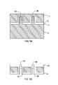
- FIGS. 1A-1Kthere is shown a series of cross-sectional views of a portion of a silicon carrier wafer which views depict a process for fabricating a conductive through via structure in such carrier, in accordance with one embodiment of the present invention.
- the cross-sectional views of a portion of a silicon carrier waferdemonstrate how one through via may be fabricated.
- FIGS. 1J and Kshow cross-sectional views of the via in a silicon die diced from the silicon carrier wafer. It is clear that a plurality of such vias may simultaneously be fabricated in a silicon wafer carrier or die, for example, using such process.
- the carrieris a silicon wafer and the insulators are oxide and nitride.
- the insulatorsare oxide and nitride.
- FIG. 1Athere is shown silicon carrier wafer 1 on silicon substrate 3 with buried oxide layer 5 and nitride layer 7 positioned therebetween.
- oxide layer 5would be 0.5 to 1.0 ⁇ m thick and nitride layer 7 would be around 0.1 ⁇ m thick.
- Nitride layer 7may be deposited by any of a variety of well known techniques, such as, CVD.
- oxide layer 5may be formed by any of a variety of well known techniques, such as, thermal oxidation or plasma enhanced CVD.
- oxide layer 5may first be deposited upon the joining side 9 of silicon wafer 1 and another portion on nitride layer 7 and then wafer 1 would be bonded to substrate 3 by fusing the oxide layers together with heat. It is clear, that other techniques could as readily be employed to bond the structures together.
- a via 11is formed in silicon wafer 1 down to oxide layer 5 . This is done by patterning photoresist layer 13 to form an opening corresponding to the desired opening size of the via and etching the silicon through the opening to lo oxide layer 5 using, for example, a deep reactive ion etch (RIE) method.
- RIEdeep reactive ion etch
- deep silicon etching by fluorine radicals generated in a plasmamay be employed.
- Such deep silicon structuresmay be fabricated using conventional available deep RIE systems, such as the A 601 E, available from Alcatel.
- silicon carrier 1may be, for example, a 200 mm wafer 50 ⁇ m thick.
- the exposed oxide of oxide layer 5 in the bottom of the viais removed stopping at nitride layer 7 .
- This oxidemay be removed by etching, for example, with HF. This is shown in FIG. 1C .
- resist layer 13is then stripped using conventional resist removing technique.
- the sidewalls of via 11are then passivated to form, for example, a layer 15 of oxide 1 ⁇ m thick using thermal oxidation. Other oxide thicknesses are also possible. This may be carried out, for example, in a tube furnace in an oxygen or steam environment between 900° C. and 1100° C.
- Via 11is then filled with a conductive material 17 .
- the conductive materialmay be plated copper or tungsten, for example.
- the materialis planarized by chemical-mechanical polishing (CMP), for example, back to the top surface of silicon carrier 1 .
- CMPchemical-mechanical polishing
- the next stepinvolves conventional silicon processing steps ending with back-end-of-line (BEOL) wiring and bond pad structures 19 .
- BEOLback-end-of-line
- Two wiring levelsare shown by way of example, with wiring level 21 connected to conductive material 17 and wiring level 23 connected to pad 25 .
- Techniques for forming such wiring and bond pad structuresare well lo known in the art.
- the term “metallurgy”is used to cover broadly conductive wiring and/or bond pad and interconnection structures similar to structures 19 .
- a temporary handling structure 27may be attached to the wiring and bond pad structure 19 , as shown in FIG. 1F .
- This handling structuremay be, for example, a glass wafer bonded to the wiring and bond pad structure 19 using an adhesive 22 .
- the next stepinvolves removing the silicon of silicon substrate 3 from the backside of the SOI structure.
- This removal processmay be accomplished by, for example, grinding and/or TMAH etch down to nitride layer 7 with latter being the etch stop.
- the next stepinvolve removal of the buried nitride layer 7 from the backside, as shown in FIG. 1H . This may be accomplished by reactive ion etching (RIE), for example. Wet etches may also be used. At this point, conductor 17 in via 11 , which is in contact with wiring 21 , is exposed.
- RIEreactive ion etching
- solder bump 29may now be deposited over the conductive through via in contact with conductive material 17 .
- a typical process for depositing solder bump 29is the well known C 4 process.
- Wafer 1may then be diced into individual die carriers 4 and flip chip joined to contact 32 on substrate 31 , as shown in FIG. 1J .
- the temporary glass handler 27is then removed by laser ablation, as shown in FIG. 1K .
- other glass handler release systemscould be employed, such as, glass handlers with an array of through holes which allow a chemical solvent to flow through the holes to remove the bonding adhesive.
- a cleaning stepis employed to remove the residual polymer on the top surface of the through via die.
- the etched via 11was filled with a conductor 17 from the front side of the multilayer SOI insulator structure.
- the process depicted in FIG. 2shows an alternative arrangement wherein the etched via 11 is filled from the front side with a non-conductor, such as, polysilicon, the latter being a convenient silicon process material.
- the polysiliconis then removed from the SOI structure from the backside and the opened via is then filled with a conductive material. Accordingly, formation of the conductive via in this arrangement is isolated from and independent of the BEOL metallization process and front-end process steps on the front side of the wafer.
- a particular advantage of using this process flowis that additional front-end process steps, such as, building transistor devices, resistors, capacitors, etc., can be carried out on the carrier since a polysilicon filled via can still be processed through front-end steps, while a metal filled via in such circumstances, typically, cannot.
- FIGS. 2A-2Care the same as previously described with respect to FIG. 1 .
- like reference charactershave been used in the various figures to identify like elements.
- the deep via resist 13has been stripped and the sidewalls passivated, as described above with respect to FIG. 1D .
- via 11is filled with polysilicon 33 . This may be done, for example, by CVD. After CVD of the polysilicon, etching or CMP of the overburden material is undertaken to planarize the surface to the silicon wafer surface.
- FIGS. 2E-2Gare the same as shown and described with respect to FIGS. 1E-1G .
- nitride layer 7is again stripped by RIE to the buried etch stop oxide layer 5 .
- the polysilicon filler plug 33 in via 11is exposed.
- the polysilicon filleris then removed using, for example, an etchant, such as, TMAH, leaving an open via 34 to the wiring 21 on the topside wiring and bond pad structure 19 .
- the open via 34is then filled with a conductive material, such as copper, to form conductive via 35 , as shown in FIG. 21 .
- a conductive materialsuch as copper
- the coppermay be plated, for example, and then planarized by CMP.
- FIG. 2includes, the additional steps of removing the polysilicon filler plug and backfilling with a conductive material from the silicon carrier wafer backside, as shown in FIGS. 2H and 2I .
- the process depicted in FIG. 3adds an additional wiring layer on the backside of wafer 1 , again, without using backside lithography.
- silicon substrate 3is first patterned with features on at least one side before silicon wafer 1 is bonded thereto.
- featuresare first patterned in the bonding side of silicon substrate 3 before bonding.
- the bonding side 37 of silicon substrate 3is etched using RIE for TMAH, for example, to form patterned recess 39 .
- the recesswould be around 0.5 ⁇ m.
- the recessed regions 39are filled with an oxide 41 and planarized using, for example, processes described above.
- blanket nitride layer 7 and a portion of the thickness of oxide layer 5are deposited over the silicon substrate surface and recessed oxide 41 , as shown in FIG. 3C .
- Wafer 1 with blanket oxide on its joining sideis then bonded to the thus formed oxide surface of bonding side 37 of substrate 3 , as shown in FIG. 3D , in a manner as described with respect to FIG. 1A .
- the bonding stepthus forms buried oxide layer 5 and nitride layer 7 of the SOI structure.
- FIGS. 3E-3Iare the same as those shown and described in FIGS. 1B-1F .
- the silicon material of silicon substrate 3is etched back to expose nitride layer 7 leaving recessed oxide 41 .
- a recess 43is thus formed for a wiring channel.
- Etches highly selective to silicon, such as, RIE or plasma etching using well known gases, such as, CF 4 , SF 6 , NF 3 , and the like,may be used for this purpose.
- the exposed nitrideis etched by RIE, for example, leaving recess region 43 between oxide pattern 41 .
- Recess region 43thus forms a channel that may be used for wiring.
- the wiring channel region 43is filled with a conductive material 45 , such as, copper.
- the coppermay, for example, be plated into the channel region and then planarized.
- This backside wiringmay be used in a variety of ways, such as, interconnecting conductive vias.
- wiring 45is used to connect conductive via 17 to solder bump 29 , as offset from the conductive via.
- FIGS. 3N and OThe structure and steps shown in FIGS. 3N and O are the same as those described with respect to FIGS. 1J and K wherein the silicon wafer 1 is diced and flip chip joined to substrate 31 . The temporary glass handler 27 is then removed by laser ablation.
- FIG. 4shows additional embodiments using sequence steps, as described above.
- silicon substrate 3is patterned with oxide 41 as described in FIG. 3 .
- the silicon between patterned oxide 41is then removed by etching and backfilled with polysilicon 5 1 .
- the thus formed silicon substrateis then bonded to silicon carrier wafer 1 , as previously described, and a pair of via conductors 47 and 49 are formed in a manner as described with respect to FIG. 1 .
- the conductors 47 and 49may, again, be copper or tungsten.
- a top oxide 53is shown, the arrangement could be implemented without it.
- silicon substrate 3has been etched back first, leaving patterned oxide 41 and polysilicon layer 51 on nitride layer 7 . Then, polysilicon layer 51 and nitride layer 7 are etched back to form a recess in the buried oxide 41 which recess may be used to form wiring.
- conductive material 54has been deposited to form a wire conductor between conductive vias 47 and 49 . It is clear that other wiring channels could, similarly, be formed.
- FIG. 5shows a further embodiment of the present invention.
- a pair of viasare etched from the backside of carrier wafer 1 , in a manner similar to that described above with respect to etching vias from the topside.
- the viasare then filed with polysilicon to form polysilicon plugs 55 and 56 in a manner as described above, and the resulting structure is bonded to silicon substrate 3 with buried oxide layer 5 and nitride layer 7 joined, as previously described.
- the silicon material of silicon substrate 3is then etched back to nitride layer 7 , and nitride layer 7 is, in turn, etched back to expose polysilicon plugs 55 and 56 , in a manner as described above.
- the silicon plugs 55 and 56are then etched out of the vias, as shown in FIG. 5B .
- the opened viasmay then be filled or lined with a conductive material 62 and conductive vias 57 and 59 formed through top oxide layer 61 .
- FIG. 6shows a combination of the structures shown in FIGS. 4 and 5 .
- FIG. 6Ashows a structure similar to FIG. 4A except for the fact that the polysilicon 51 , shown in FIG. 4A , extends up into the vias (like FIG. 5 A) where conductors 47 and 49 are shown, to thereby form polysilicon region 63 .
- insulating layer 67On substrate 3 , then nitride layer 65 on insulating layer 67 and then insulating layer 71 on nitride layer 65 , as shown in FIG. 6A , all before joining substrate 3 to carrier wafer 1 .
- Lithographyis then used to a pattern an opening in insulating layer 71 and the opening is backfilled with polysilicon 63 .
- Polysiliconis also separately backfilled into vias in silicon carrier 1 through a patterned nitride layer 69 , similar to the process employed in FIG. 5 , to thereby form polysilicon regions 55 and 56 .
- Substrate 3thus formed, is then bonded to carrier 1 , thus formed.
- Etchingis then carried out, as previously described, to produce vias that open to a common channel region 71 , as shown in FIG. 6B .
- the vias, channel region and common port 73may then be plated with a conductive material 75 .
Landscapes
- Engineering & Computer Science (AREA)
- Physics & Mathematics (AREA)
- Condensed Matter Physics & Semiconductors (AREA)
- General Physics & Mathematics (AREA)
- Computer Hardware Design (AREA)
- Microelectronics & Electronic Packaging (AREA)
- Power Engineering (AREA)
- Manufacturing & Machinery (AREA)
- Ceramic Engineering (AREA)
- Internal Circuitry In Semiconductor Integrated Circuit Devices (AREA)
Abstract
Description
- 1. Field of the Invention
- The present invention relates to electrically interconnecting via structures and methods of making same in material, such as, semiconductor material. More particularly, the present invention relates to conductive through via structures and processes for making same in electronic device lo structures, such as in semiconductor wafers, semiconductor chips, components and the like, and in electronic device carriers for such semiconductor wafers, chips, components, and the like.
- 2. Background and Related Art In the packaging of electronic devices, such as, semiconductor chips or wafers, device carriers may be used to interconnect the devices. Where electronic devices are connected to another level of packaging, the carriers typically require conductive vias extending through the carrier to connect the devices to the next level of packaging.
- Electronic device carriers may be fabricated from a variety of different materials, such as, glass, ceramic, organic and semiconductor materials or combinations of these and other materials in single or multiple layers.
- Electronic device carriers made of semiconductor material, such as, silicon, offer a number of advantages in packaging, such as, ease of manufacturing and reliability and high connection density One of the challenges with this technology is the requirement for complex processing to be carried out on the backside of the wafer. Conventional complex processing steps involving lithography, RIE etching and the like may become much more difficult and costly when carried out on the backside of a semiconductor carrier, such as, silicon.
- One prior art approach to creating conductive vias in semiconductor carriers, such as silicon, use what might be called a “via first” approach. The general steps in such an approach are etching the vias, forming insulation layers on the via walls and metallization. When a “blind via” approach is used, the vias are not etched through the wafer layer so that a “through via” is rendered only after the carrier is suitably thinned to expose the via bottoms. An example of such an approach may be seen in U.S. Pat. No. 5,998,292.
- There are, however, a number of difficulties with this type of approach. For example, one difficulty is controlling vertical structure dimensions. Another difficulty is controlling the backside thinning depth stop and isolation of the process steps.
- Some approaches to creating through vias in semiconductor carriers may require backside lithographic processing and etching steps. Such processing on the backside of a silicon carrier, adds to processing complexity. As an example, U.S. application Ser. No. 11/214,602 filed Aug. 30, 2005, and assigned to the assignee of the present invention, uses photolithography and RIE processing steps on the backside of a silicon wafer in forming through vias in the wafer.
- It is an object of the present invention to provide an improved electronic structure and method for fabricating same.
- It is a further object of the present invention to provide an improved method of making conductive via structures for electronic packaging.
- It is yet a further object of the present invention to provide a through via structure and improved method for making same that simplifies fabrication and improves yield and reliability of packaged electronic devices.
- It is yet still a further object of the present invention to provide an improved through via structure and method of making same which readily allows vias to be fabricated of different diameters of uniform depth on a single electronic structure, such as, a chip carrier structure.
- It is yet another object of the present invention to provide an improved through via structure and method of making which decouples the via metallization process step from the frontside back-end-of-line (BEOL) metallization process.
- It is still yet another object of the present invention to provide a process for fabrication of through conductive via structures in a silicon carrier using a silicon-on-insulator (SOI) wafer structure that provides controlled depth stop and isolation, and simplifies backside processing and in which all structures are self-aligned and structure vertical dimensions tightly controlled.
- These, as well as other objects, are achieved in the present invention by forming conductive through vias using a pair of semiconductor structures bonded together through at least two layers of insulation to form a buried insulation structure. More particularly, the method of the present invention comprises the steps of:
- providing a semiconductor structure including a first layer of semiconductor material having first and second surfaces and second a layer of semiconductor material having first and second surfaces joined together by a first layer of insulating material and a second layer of insulating material with said first layer of insulating material interposed between said second layer of insulating material and the said second surface of said first layer of semiconductor material and said second layer of insulating material interposed between said first layer of insulating material and the said second surface of said second layer of semiconductor material;
- forming a via in said first layer of semiconductor material having a wall surface extending from the said first surface of said first layer of semiconductor material through said first layer of insulating material to said second layer of insulating material;
- forming a layer of insulating material on the said wall surface of said via;
- filling said via with another material;
- etching said second layer of semiconductor material back to said second layer of insulating material; and
- etching said second layer of insulating material to expose said another material.
- As further provided by the present invention, wherein said layer of insulating material on said wall surface of said via is made of the same insulating material as said first layer of insulating material.
- As still further provided by the present invention wherein said first layer of semiconductor material and said second layer of semiconductor material are both silicon.
- As yet still further provided by the present invention, the step of providing conductive wiring material on said another material.
- As still further provided by the present invention, wherein said another material is a conductive material.
- As yet further provided by the present invention wherein said another material is polysilicon.
- As still further provided by the present invention, the method includes the steps of;
- providing an SOI wafer structure including at least a first layer of insulating material and a second layer of insulating material formed between a silicon wafer and silicon substrate with said first layer on insulating material in contact with said silicon wafer;
- etching a via from the top surface of said silicon wafer through to said first insulating layer;
- etching through said first layer of insulating material;
- forming an insulating layer on the sidewalls of said etched via made of the same material as said first layer of insulating material;
- filling said via with polysilicon material and planarizing to said top surface of said silicon wafer;
- forming conductive metallurgy over said polysilicon material; and then
- removing by etching said silicon substrate; then
- removing by etching said second layer of insulating material; then
- removing by etching said polysilicon material to again form an open via; and
- forming conductive material in said via to connect to said conductive metallurgy.
- As also provided by the present invention, an electrical contact, such as, a solder bump, is formed in contact with said conductive material in said via.
- As further provided by the present invention, internal wiring channels are formed between conductive vias in accordance with the process SOI steps described.
- In one embodiment of the present invention, a SOI structure is provided having a silicon substrate with a nitride layer formed thereon. An oxide layer is formed on the nitride layer and a silicon carrier wafer is attached to said oxide layer. The walls of a via, formed through the silicon carrier wafer and the buried oxide layer to the nitride layer, are oxidized and back filled with another material. Metallurgy is then formed over said another material.
- In another embodiment of the present invention, the above silicon substrate is removed leaving said nitride layer. The nitride layer is then removed leaving said another material. Removal of said another material forms an open via to said metallurgy. Conductive material, back filled into the via, provides electrical connection to said metallurgy. A solder bump is formed in contact with the conductive material formed in the via to permit, for example, connection to a substrate. The thus formed wafer provides a relatively thick silicon carrier.
- In another embodiment, the above back filled another material is conductive material thereby providing electrical connection to said metallurgy without the need for backside via etching and backfilling with a conductive material.
- In a further embodiment of the present invention, the silicon carrier wafer backside is provided with backside wiring.
- In yet still a further embodiment of the present invention, the vias are first created in the silicon carrier wafer from the backside and filled with polysilicon prior to bonding to the silicon substrate.
- In another embodiment of the present invention, the silicon carrier wafer is provided with internal wiring channels interconnecting conductive vias.
FIGS. 1A-1K show a series of process steps for fabricating a carrier structure, in accordance with one embodiment of the invention.FIGS. 2A-2L show a series of process steps for fabricating a carrier structure, in accordance with another embodiment of the present invention.FIGS. 3A-30 show a series of process steps for fabricating carrier structure, in accordance with yet another embodiment of the present invention.FIGS. 4A-4C show a series of process steps for fabricating yet another carrier structure, in accordance with yet still another embodiment of the present invention.FIGS. 5A-5B show further process steps for fabricating a carrier structure, in accordance a further embodiment of the present invention.FIGS. 6A-6C show steps for fabricating a carrier structure, in accordance with yet a further embodiment of the present invention.- In accordance with the present invention, conductive through vias in electronic device structures, such as, semiconductor wafer and chip structures and the like, and in electronic device carriers for same are provided by using semiconductor-on-insulator arrangements. As more particularly described, silicon-on-insulator (SOI) structures may be used. Multilayer SOI insulator structures are used to provide a backside lithography-free process for forming vias and channels in a silicon wafer. The SOI wafer structure process provides for controlled depth stop and isolation in through via formation and simplifies backside processing, as may be employed, for example, in silicon carrier technology.
- Although description of the via structure and method for fabricating same are described in the following embodiments in terms of electronic device silicon carrier structures, it should be understood that the via structure and method for fabricating same may also be formed in other electronic structures, such as, active device chip and wafer structures. For example, the via structure and method for fabricating same may be used in device stacking, such as, wafer-to-wafer stacking and chip-to-chip stacking. It is readily apparent that the via structure and process of making same defined by the present invention may be employed in any of a variety of electronic device structures, such as, image sensors with backside contact requirements. Although reference is made to silicon structures, it is also readily apparent that structures of other semiconductor material may also be used.
- With reference to
FIGS. 1A-1K there is shown a series of cross-sectional views of a portion of a silicon carrier wafer which views depict a process for fabricating a conductive through via structure in such carrier, in accordance with one embodiment of the present invention. The cross-sectional views of a portion of a silicon carrier wafer, as shown inFIGS. 1A to 1I , demonstrate how one through via may be fabricated.FIGS. 1J and K show cross-sectional views of the via in a silicon die diced from the silicon carrier wafer. It is clear that a plurality of such vias may simultaneously be fabricated in a silicon wafer carrier or die, for example, using such process. - In the presently preferred embodiment, the carrier is a silicon wafer and the insulators are oxide and nitride. However, other insulators may also be used. With reference to
FIG. 1A , there is shownsilicon carrier wafer 1 onsilicon substrate 3 with buriedoxide layer 5 andnitride layer 7 positioned therebetween. Typically,oxide layer 5 would be 0.5 to 1.0 μm thick andnitride layer 7 would be around 0.1 μm thick.Nitride layer 7 may be deposited by any of a variety of well known techniques, such as, CVD. Similarly,oxide layer 5 may be formed by any of a variety of well known techniques, such as, thermal oxidation or plasma enhanced CVD. In this regard, a portion ofoxide layer 5 may first be deposited upon the joiningside 9 ofsilicon wafer 1 and another portion onnitride layer 7 and thenwafer 1 would be bonded tosubstrate 3 by fusing the oxide layers together with heat. It is clear, that other techniques could as readily be employed to bond the structures together. - After forming the multilayer SOI structure shown in
FIG. 1A , a via11 is formed insilicon wafer 1 down tooxide layer 5. This is done by patterningphotoresist layer 13 to form an opening corresponding to the desired opening size of the via and etching the silicon through the opening tolo oxide layer 5 using, for example, a deep reactive ion etch (RIE) method. Thus, deep silicon etching by fluorine radicals generated in a plasma, as is known in the art, may be employed. Such deep silicon structures may be fabricated using conventional available deep RIE systems, such as the A601E, available from Alcatel. In this regard, it is noted that, in accordance with the process of the present invention,silicon carrier 1 may be, for example, a 200 mm wafer 50 μm thick. - After etching via11, the exposed oxide of
oxide layer 5 in the bottom of the via is removed stopping atnitride layer 7. This oxide may be removed by etching, for example, with HF. This is shown inFIG. 1C . - As shown in
FIG. 1D , resistlayer 13 is then stripped using conventional resist removing technique. As also shown inFIG. 1D , the sidewalls of via11 are then passivated to form, for example, alayer 15 ofoxide 1 μm thick using thermal oxidation. Other oxide thicknesses are also possible. This may be carried out, for example, in a tube furnace in an oxygen or steam environment between 900° C. and 1100°C. Via 11 is then filled with aconductive material 17. The conductive material may be plated copper or tungsten, for example. After filling the via with a conductive material, the material is planarized by chemical-mechanical polishing (CMP), for example, back to the top surface ofsilicon carrier 1. - As shown in
FIG. 1E , the next step involves conventional silicon processing steps ending with back-end-of-line (BEOL) wiring andbond pad structures 19. Two wiring levels are shown by way of example, withwiring level 21 connected toconductive material 17 andwiring level 23 connected to pad25. Techniques for forming such wiring and bond pad structures are well lo known in the art. In this regard, the term “metallurgy” is used to cover broadly conductive wiring and/or bond pad and interconnection structures similar tostructures 19. - For convenience in handling, a
temporary handling structure 27 may be attached to the wiring andbond pad structure 19, as shown inFIG. 1F . This handling structure may be, for example, a glass wafer bonded to the wiring andbond pad structure 19 using an adhesive22. - As shown in
FIG. 1G , the next step involves removing the silicon ofsilicon substrate 3 from the backside of the SOI structure. This removal process may be accomplished by, for example, grinding and/or TMAH etch down tonitride layer 7 with latter being the etch stop. - The next step involve removal of the buried
nitride layer 7 from the backside, as shown inFIG. 1H . This may be accomplished by reactive ion etching (RIE), for example. Wet etches may also be used. At this point,conductor 17 in via11, which is in contact withwiring 21, is exposed. - As shown in
FIG. 11 , asolder bump 29 may now be deposited over the conductive through via in contact withconductive material 17. A typical process for depositingsolder bump 29 is the well known C4 process. Wafer 1 may then be diced intoindividual die carriers 4 and flip chip joined to contact32 onsubstrate 31, as shown inFIG. 1J . Thetemporary glass handler 27 is then removed by laser ablation, as shown inFIG. 1K . It is clear that other glass handler release systems could be employed, such as, glass handlers with an array of through holes which allow a chemical solvent to flow through the holes to remove the bonding adhesive. After removal of lo the glass handler, a cleaning step is employed to remove the residual polymer on the top surface of the through via die.- In the process depicted in
FIG. 1 , it is noted that the etched via11 was filled with aconductor 17 from the front side of the multilayer SOI insulator structure. The process depicted inFIG. 2 shows an alternative arrangement wherein the etched via11 is filled from the front side with a non-conductor, such as, polysilicon, the latter being a convenient silicon process material. In such an arrangement, the polysilicon is then removed from the SOI structure from the backside and the opened via is then filled with a conductive material. Accordingly, formation of the conductive via in this arrangement is isolated from and independent of the BEOL metallization process and front-end process steps on the front side of the wafer. Thus, a particular advantage of using this process flow is that additional front-end process steps, such as, building transistor devices, resistors, capacitors, etc., can be carried out on the carrier since a polysilicon filled via can still be processed through front-end steps, while a metal filled via in such circumstances, typically, cannot. - Thus, in the process arrangement of
FIG. 2 ,FIGS. 2A-2C are the same as previously described with respect toFIG. 1 . In this regard, like reference characters have been used in the various figures to identify like elements. InFIG. 2D , the deep via resist13 has been stripped and the sidewalls passivated, as described above with respect toFIG. 1D . However, at this point via11 is filled withpolysilicon 33. This may be done, for example, by CVD. After CVD of the polysilicon, etching or CMP of the overburden material is undertaken to planarize the surface to the silicon wafer surface. - Conventional silicon processing steps are then undertaken to add front end devices and BEOL wiring and bond pad structures, as shown in
FIG. 2E . The structure and steps shown inFIGS. 2E-2G are the same as shown and described with respect toFIGS. 1E-1G . - As shown in
FIG. 2H ,nitride layer 7 is again stripped by RIE to the buried etchstop oxide layer 5. At this point, thepolysilicon filler plug 33 in via11 is exposed. The polysilicon filler is then removed using, for example, an etchant, such as, TMAH, leaving an open via34 to thewiring 21 on the topside wiring andbond pad structure 19. - The open via34 is then filled with a conductive material, such as copper, to form conductive via35, as shown in
FIG. 21 . The copper may be plated, for example, and then planarized by CMP. - The remaining steps shown in
FIGS. 2J-2L are the same as described and shown with respect toFIGS. 1I-1K above. Thus,FIG. 2 includes, the additional steps of removing the polysilicon filler plug and backfilling with a conductive material from the silicon carrier wafer backside, as shown inFIGS. 2H and 2I . - The process depicted in
FIG. 3 adds an additional wiring layer on the backside ofwafer 1, again, without using backside lithography. In such an arrangement,silicon substrate 3 is first patterned with features on at least one side beforesilicon wafer 1 is bonded thereto. In the arrangement ofFIG. 3 , features are first patterned in the bonding side ofsilicon substrate 3 before bonding. - Thus, as shown in
FIG. 3A , thebonding side 37 ofsilicon substrate 3 is etched using RIE for TMAH, for example, to form patternedrecess 39. Typically, the recess would be around 0.5 μm. InFIG. 3B , the recessedregions 39 are filled with anoxide 41 and planarized using, for example, processes described above. After planarizingoxide 41,blanket nitride layer 7 and a portion of the thickness ofoxide layer 5 are deposited over the silicon substrate surface and recessedoxide 41, as shown inFIG. 3C .Wafer 1 with blanket oxide on its joining side is then bonded to the thus formed oxide surface of bondingside 37 ofsubstrate 3, as shown inFIG. 3D , in a manner as described with respect toFIG. 1A . The bonding step thus forms buriedoxide layer 5 andnitride layer 7 of the SOI structure. - The structure and steps shown in
FIGS. 3E-3I are the same as those shown and described inFIGS. 1B-1F . However, as shown inFIG. 3J , the silicon material ofsilicon substrate 3 is etched back to exposenitride layer 7 leaving recessedoxide 41. Arecess 43 is thus formed for a wiring channel. Etches highly selective to silicon, such as, RIE or plasma etching using well known gases, such as, CF4, SF6, NF3, and the like, may be used for this purpose. - As shown in
FIG. 3K , the exposed nitride is etched by RIE, for example, leavingrecess region 43 betweenoxide pattern 41.Recess region 43 thus forms a channel that may be used for wiring. As shown inFIG. 3L , thewiring channel region 43 is filled with aconductive material 45, such as, copper. The copper may, for example, be plated into the channel region and then planarized. - This backside wiring may be used in a variety of ways, such as, interconnecting conductive vias. In
FIG. 3M , wiring45 is used to connect conductive via17 tosolder bump 29, as offset from the conductive via. The structure and steps shown inFIGS. 3N and O are the same as those described with respect toFIGS. 1J and K wherein thesilicon wafer 1 is diced and flip chip joined tosubstrate 31. Thetemporary glass handler 27 is then removed by laser ablation. FIG. 4 shows additional embodiments using sequence steps, as described above. InFIG. 4A , before joining tosilicon carrier wafer 1,silicon substrate 3 is patterned withoxide 41 as described inFIG. 3 . The silicon between patternedoxide 41 is then removed by etching and backfilled withpolysilicon 51. The thus formed silicon substrate is then bonded tosilicon carrier wafer 1, as previously described, and a pair of viaconductors FIG. 1 . Theconductors top oxide 53 is shown, the arrangement could be implemented without it.- In
FIG. 4B ,silicon substrate 3 has been etched back first, leavingpatterned oxide 41 andpolysilicon layer 51 onnitride layer 7. Then,polysilicon layer 51 andnitride layer 7 are etched back to form a recess in the buriedoxide 41 which recess may be used to form wiring. InFIG. 4C ,conductive material 54 has been deposited to form a wire conductor betweenconductive vias FIG. 5 shows a further embodiment of the present invention. In this embodiment, beforesilicon wafer 1 is bonded tosilicon substrate 3, a pair of vias are etched from the backside ofcarrier wafer 1, in a manner similar to that described above with respect to etching vias from the topside. The vias are then filed with polysilicon to form polysilicon plugs55 and56 in a manner as described above, and the resulting structure is bonded tosilicon substrate 3 with buriedoxide layer 5 andnitride layer 7 joined, as previously described.- The silicon material of
silicon substrate 3 is then etched back tonitride layer 7, andnitride layer 7 is, in turn, etched back to expose polysilicon plugs55 and56, in a manner as described above. The silicon plugs55 and56 are then etched out of the vias, as shown inFIG. 5B . As also shown inFIG. 5B , the opened vias may then be filled or lined with aconductive material 62 andconductive vias top oxide layer 61. FIG. 6 shows a combination of the structures shown inFIGS. 4 and 5 .FIG. 6A shows a structure similar toFIG. 4A except for the fact that thepolysilicon 51, shown inFIG. 4A , extends up into the vias (like FIG.5A) whereconductors polysilicon region 63.- This may be accomplished by forming insulating
layer 67 onsubstrate 3, thennitride layer 65 on insulatinglayer 67 and then insulatinglayer 71 onnitride layer 65, as shown inFIG. 6A , all before joiningsubstrate 3 tocarrier wafer 1. Lithography is then used to a pattern an opening in insulatinglayer 71 and the opening is backfilled withpolysilicon 63. Polysilicon is also separately backfilled into vias insilicon carrier 1 through a patternednitride layer 69, similar to the process employed inFIG. 5 , to thereby formpolysilicon regions Substrate 3, thus formed, is then bonded tocarrier 1, thus formed. - Etching is then carried out, as previously described, to produce vias that open to a
common channel region 71, as shown inFIG. 6B . As shown inFIG. 6C , the vias, channel region andcommon port 73 may then be plated with aconductive material 75. - It will be understood from the foregoing description that various modifications and changes may be made in the preferred embodiment of the present invention without departing from its true spirit. It is intended that this description is for purposes of illustration only and should not be construed in a limiting sense. The scope of this invention should be limited only by the language of the following claims.
Claims (20)
Priority Applications (3)
| Application Number | Priority Date | Filing Date | Title |
|---|---|---|---|
| US11/751,105US7645701B2 (en) | 2007-05-21 | 2007-05-21 | Silicon-on-insulator structures for through via in silicon carriers |
| CN2008100952822ACN101312161B (en) | 2007-05-21 | 2008-05-09 | Electronic structures and fabrication methods thereof |
| US12/550,494US8198734B2 (en) | 2007-05-21 | 2009-08-31 | Silicon-on-insulator structures for through via in silicon carriers |
Applications Claiming Priority (1)
| Application Number | Priority Date | Filing Date | Title |
|---|---|---|---|
| US11/751,105US7645701B2 (en) | 2007-05-21 | 2007-05-21 | Silicon-on-insulator structures for through via in silicon carriers |
Related Child Applications (1)
| Application Number | Title | Priority Date | Filing Date |
|---|---|---|---|
| US12/550,494DivisionUS8198734B2 (en) | 2007-05-21 | 2009-08-31 | Silicon-on-insulator structures for through via in silicon carriers |
Publications (2)
| Publication Number | Publication Date |
|---|---|
| US20080290525A1true US20080290525A1 (en) | 2008-11-27 |
| US7645701B2 US7645701B2 (en) | 2010-01-12 |
Family
ID=40071653
Family Applications (2)
| Application Number | Title | Priority Date | Filing Date |
|---|---|---|---|
| US11/751,105Active2027-12-04US7645701B2 (en) | 2007-05-21 | 2007-05-21 | Silicon-on-insulator structures for through via in silicon carriers |
| US12/550,494Expired - Fee RelatedUS8198734B2 (en) | 2007-05-21 | 2009-08-31 | Silicon-on-insulator structures for through via in silicon carriers |
Family Applications After (1)
| Application Number | Title | Priority Date | Filing Date |
|---|---|---|---|
| US12/550,494Expired - Fee RelatedUS8198734B2 (en) | 2007-05-21 | 2009-08-31 | Silicon-on-insulator structures for through via in silicon carriers |
Country Status (2)
| Country | Link |
|---|---|
| US (2) | US7645701B2 (en) |
| CN (1) | CN101312161B (en) |
Cited By (17)
| Publication number | Priority date | Publication date | Assignee | Title |
|---|---|---|---|---|
| US20100207271A1 (en)* | 2009-02-19 | 2010-08-19 | Toshihiko Omi | Semiconductor device |
| US20110266674A1 (en)* | 2010-04-28 | 2011-11-03 | Taiwan Semiconductor Manufacturing Company, Ltd. | Laser Etch Via Formation |
| US20110284984A1 (en)* | 2010-05-18 | 2011-11-24 | Chih-Min Liu | Image sensor and fabricating method thereof |
| US20140057434A1 (en)* | 2012-08-24 | 2014-02-27 | Jia-Jia Chen | Through silicon via process |
| NL2009757C2 (en)* | 2012-11-05 | 2014-05-08 | Micronit Microfluidics Bv | Method for forming an electrically conductive via in a substrate. |
| US20150130077A1 (en)* | 2010-09-17 | 2015-05-14 | Tessera, Inc. | Staged via formation from both sides of chip |
| US20150187647A1 (en)* | 2013-12-26 | 2015-07-02 | Globalfoundries Singapore Pte. Ltd. | Through via contacts with insulated substrate |
| US20150255344A1 (en)* | 2012-09-27 | 2015-09-10 | Silex Microsystems Ab | Electroless metal through silicon via |
| EP2831913A4 (en)* | 2012-03-30 | 2015-12-16 | Silex Microsystems Ab | METHOD OF MAKING AN INTERCONNECTION HOLE AND A ROUTING STRUCTURE |
| FR3037720A1 (en)* | 2015-06-19 | 2016-12-23 | St Microelectronics Crolles 2 Sas | ELECTRONIC COMPONENT AND METHOD FOR MANUFACTURING THE SAME |
| JP2017500731A (en)* | 2013-10-28 | 2017-01-05 | オスラム オプト セミコンダクターズ ゲゼルシャフト ミット ベシュレンクテル ハフツングOsram Opto Semiconductors GmbH | Optoelectronic component and manufacturing method thereof |
| US20200135636A1 (en)* | 2018-10-24 | 2020-04-30 | Samsung Electronics Co., Ltd. | Semiconductor package |
| CN112292760A (en)* | 2018-06-21 | 2021-01-29 | 索泰克公司 | Front-side image sensor and method of making the same |
| CN113013094A (en)* | 2021-02-24 | 2021-06-22 | 长江存储科技有限责任公司 | Semiconductor device and manufacturing method thereof |
| CN115274548A (en)* | 2021-04-29 | 2022-11-01 | 苏州华太电子技术股份有限公司 | SOI wafer and manufacturing method of TSV in SOI wafer |
| US20230011266A1 (en)* | 2021-07-12 | 2023-01-12 | Changxin Memory Technologies, Inc. | Method for forming semiconductor structure |
| WO2024110940A1 (en)* | 2022-11-27 | 2024-05-30 | Teracyte Analytics Ltd. | Silicon-on-insulator (soi) carrier chip and methods of manufacture thereof |
Families Citing this family (18)
| Publication number | Priority date | Publication date | Assignee | Title |
|---|---|---|---|---|
| US7645701B2 (en)* | 2007-05-21 | 2010-01-12 | International Business Machines Corporation | Silicon-on-insulator structures for through via in silicon carriers |
| US8587121B2 (en)* | 2010-03-24 | 2013-11-19 | International Business Machines Corporation | Backside dummy plugs for 3D integration |
| US8316717B2 (en) | 2010-06-29 | 2012-11-27 | Rogue Valley Microdevices, Inc. | Wireless self-powered monolithic integrated capacitive sensor and method of manufacture |
| US8492260B2 (en) | 2010-08-30 | 2013-07-23 | Semionductor Components Industries, LLC | Processes of forming an electronic device including a feature in a trench |
| CN102420234B (en)* | 2010-09-28 | 2015-04-08 | 汉积科技股份有限公司 | Manufacturing method of photosensitive structure |
| CN102064092B (en)* | 2010-10-26 | 2012-09-05 | 日月光半导体制造股份有限公司 | Carrier separation method for semiconductor process |
| FR2980917B1 (en)* | 2011-09-30 | 2013-09-27 | St Microelectronics Crolles 2 | METHOD FOR PRODUCING AN ELECTRICALLY CONDUCTIVE THROUGH BOND |
| US9236274B1 (en)* | 2011-11-01 | 2016-01-12 | Triton Microtechnologies | Filling materials and methods of filling through holes for improved adhesion and hermeticity in glass substrates and other electronic components |
| CN103579088B (en)* | 2012-07-26 | 2016-09-21 | 中芯国际集成电路制造(上海)有限公司 | A kind of preparation method of semiconductor device silicon through hole |
| US8981533B2 (en) | 2012-09-13 | 2015-03-17 | Semiconductor Components Industries, Llc | Electronic device including a via and a conductive structure, a process of forming the same, and an interposer |
| US9000344B2 (en)* | 2013-03-15 | 2015-04-07 | Sensors Unlimited, Inc. | Focal plane array periphery through-vias for read out integrated circuit |
| US9831281B2 (en) | 2015-05-01 | 2017-11-28 | Sensors Unlimited, Inc. | Electrical interconnects for photodiode arrays and readout interface circuits in focal plane array assemblies |
| US9812354B2 (en) | 2015-05-15 | 2017-11-07 | Semiconductor Components Industries, Llc | Process of forming an electronic device including a material defining a void |
| US9455187B1 (en) | 2015-06-18 | 2016-09-27 | International Business Machines Corporation | Backside device contact |
| US9514987B1 (en) | 2015-06-19 | 2016-12-06 | International Business Machines Corporation | Backside contact to final substrate |
| US9496239B1 (en)* | 2015-12-11 | 2016-11-15 | International Business Machines Corporation | Nitride-enriched oxide-to-oxide 3D wafer bonding |
| US11056382B2 (en) | 2018-03-19 | 2021-07-06 | Globalfoundries U.S. Inc. | Cavity formation within and under semiconductor devices |
| EP3937512A1 (en)* | 2020-07-10 | 2022-01-12 | Infineon Technologies AG | Method and structure for sensors on glass |
Citations (10)
| Publication number | Priority date | Publication date | Assignee | Title |
|---|---|---|---|---|
| US5218213A (en)* | 1991-02-22 | 1993-06-08 | Harris Corporation | SOI wafer with sige |
| US5312621A (en)* | 1988-01-25 | 1994-05-17 | Baker Cummins Dermatologicals, Inc. | Method of treating fibrotic disorders |
| US5998292A (en)* | 1997-11-12 | 1999-12-07 | International Business Machines Corporation | Method for making three dimensional circuit integration |
| US20020146867A1 (en)* | 2000-12-29 | 2002-10-10 | Stmicroelectronics S.R.L. | Integration process on a SOI substrate of a semiconductor device comprising at least a dielectrically isolated well |
| US6770542B2 (en)* | 2001-12-20 | 2004-08-03 | Osram Opto Semiconductors Gmbh | Method for fabricating semiconductor layers |
| US6888223B2 (en)* | 2003-04-01 | 2005-05-03 | International Business Machines Corporation | Use of photoresist in substrate vias during backside grind |
| US6897125B2 (en)* | 2003-09-17 | 2005-05-24 | Intel Corporation | Methods of forming backside connections on a wafer stack |
| US20050121768A1 (en)* | 2003-12-05 | 2005-06-09 | International Business Machines Corporation | Silicon chip carrier with conductive through-vias and method for fabricating same |
| US20070111538A1 (en)* | 2005-11-12 | 2007-05-17 | Applied Materials, Inc. | Method of fabricating a silicon nitride stack |
| US20080164573A1 (en)* | 2007-01-05 | 2008-07-10 | Basker Veeraraghaven S | Methods for fabricating silicon carriers with conductive through-vias with low stress and low defect density |
Family Cites Families (19)
| Publication number | Priority date | Publication date | Assignee | Title |
|---|---|---|---|---|
| US5666002A (en)* | 1993-06-22 | 1997-09-09 | Kabushiki Kaisha Toshiba | Semiconductor device with wiring layer in tunnel in semiconductor substrate |
| US5682062A (en)* | 1995-06-05 | 1997-10-28 | Harris Corporation | System for interconnecting stacked integrated circuits |
| US6312621B1 (en) | 1998-11-17 | 2001-11-06 | Johnson Matthey Electronics, Inc. | Via fill formulations which are electrically and/or thermally conductive, or non-conductive |
| US6835589B2 (en)* | 2002-11-14 | 2004-12-28 | International Business Machines Corporation | Three-dimensional integrated CMOS-MEMS device and process for making the same |
| JP4086673B2 (en)* | 2003-02-04 | 2008-05-14 | Necエレクトロニクス株式会社 | Semiconductor device and manufacturing method thereof |
| JP2004311948A (en)* | 2003-03-27 | 2004-11-04 | Seiko Epson Corp | Semiconductor device, semiconductor device, electronic device, and method of manufacturing semiconductor device |
| US7151315B2 (en)* | 2003-06-11 | 2006-12-19 | Taiwan Semiconductor Manufacturing Company, Ltd. | Method of a non-metal barrier copper damascene integration |
| JP3646720B2 (en)* | 2003-06-19 | 2005-05-11 | セイコーエプソン株式会社 | Semiconductor device and manufacturing method thereof, circuit board, and electronic apparatus |
| CN1294640C (en)* | 2003-09-03 | 2007-01-10 | 联华电子股份有限公司 | Via-first dual damascene process |
| JP4432470B2 (en)* | 2003-11-25 | 2010-03-17 | 株式会社デンソー | Semiconductor device |
| US7060601B2 (en)* | 2003-12-17 | 2006-06-13 | Tru-Si Technologies, Inc. | Packaging substrates for integrated circuits and soldering methods |
| JP2008507837A (en)* | 2004-07-20 | 2008-03-13 | コーニンクレッカ フィリップス エレクトロニクス エヌ ヴィ | Semiconductor device and manufacturing method of semiconductor device |
| KR100641362B1 (en)* | 2005-01-13 | 2006-10-31 | 삼성전자주식회사 | Wiring structure with double diffusion barrier and manufacturing method |
| JP2007036060A (en)* | 2005-07-28 | 2007-02-08 | Sanyo Electric Co Ltd | Semiconductor device and manufacturing method thereof |
| US7772116B2 (en)* | 2005-09-01 | 2010-08-10 | Micron Technology, Inc. | Methods of forming blind wafer interconnects |
| US7410884B2 (en)* | 2005-11-21 | 2008-08-12 | Intel Corporation | 3D integrated circuits using thick metal for backside connections and offset bumps |
| US7605019B2 (en)* | 2006-07-07 | 2009-10-20 | Qimonda Ag | Semiconductor device with stacked chips and method for manufacturing thereof |
| US7344959B1 (en)* | 2006-07-25 | 2008-03-18 | International Business Machines Corporation | Metal filled through via structure for providing vertical wafer-to-wafer interconnection |
| US7645701B2 (en)* | 2007-05-21 | 2010-01-12 | International Business Machines Corporation | Silicon-on-insulator structures for through via in silicon carriers |
- 2007
- 2007-05-21USUS11/751,105patent/US7645701B2/enactiveActive
- 2008
- 2008-05-09CNCN2008100952822Apatent/CN101312161B/ennot_activeExpired - Fee Related
- 2009
- 2009-08-31USUS12/550,494patent/US8198734B2/ennot_activeExpired - Fee Related
Patent Citations (13)
| Publication number | Priority date | Publication date | Assignee | Title |
|---|---|---|---|---|
| US5312621A (en)* | 1988-01-25 | 1994-05-17 | Baker Cummins Dermatologicals, Inc. | Method of treating fibrotic disorders |
| US5218213A (en)* | 1991-02-22 | 1993-06-08 | Harris Corporation | SOI wafer with sige |
| US5998292A (en)* | 1997-11-12 | 1999-12-07 | International Business Machines Corporation | Method for making three dimensional circuit integration |
| US20020146867A1 (en)* | 2000-12-29 | 2002-10-10 | Stmicroelectronics S.R.L. | Integration process on a SOI substrate of a semiconductor device comprising at least a dielectrically isolated well |
| US6770542B2 (en)* | 2001-12-20 | 2004-08-03 | Osram Opto Semiconductors Gmbh | Method for fabricating semiconductor layers |
| US7074715B2 (en)* | 2003-04-01 | 2006-07-11 | International Business Machines Corporation | Use of photoresist in substrate vias during backside grind |
| US6888223B2 (en)* | 2003-04-01 | 2005-05-03 | International Business Machines Corporation | Use of photoresist in substrate vias during backside grind |
| US6897125B2 (en)* | 2003-09-17 | 2005-05-24 | Intel Corporation | Methods of forming backside connections on a wafer stack |
| US7056813B2 (en)* | 2003-09-17 | 2006-06-06 | Intel Corporation | Methods of forming backside connections on a wafer stack |
| US20060027934A1 (en)* | 2003-12-05 | 2006-02-09 | International Business Machines Corporation | Silicon chip carrier with conductive through-vias and method for fabricating same |
| US20050121768A1 (en)* | 2003-12-05 | 2005-06-09 | International Business Machines Corporation | Silicon chip carrier with conductive through-vias and method for fabricating same |
| US20070111538A1 (en)* | 2005-11-12 | 2007-05-17 | Applied Materials, Inc. | Method of fabricating a silicon nitride stack |
| US20080164573A1 (en)* | 2007-01-05 | 2008-07-10 | Basker Veeraraghaven S | Methods for fabricating silicon carriers with conductive through-vias with low stress and low defect density |
Cited By (38)
| Publication number | Priority date | Publication date | Assignee | Title |
|---|---|---|---|---|
| US20100207271A1 (en)* | 2009-02-19 | 2010-08-19 | Toshihiko Omi | Semiconductor device |
| US20110266674A1 (en)* | 2010-04-28 | 2011-11-03 | Taiwan Semiconductor Manufacturing Company, Ltd. | Laser Etch Via Formation |
| US8519538B2 (en)* | 2010-04-28 | 2013-08-27 | Taiwan Semiconductor Manufacturing Company, Ltd. | Laser etch via formation |
| US20110284984A1 (en)* | 2010-05-18 | 2011-11-24 | Chih-Min Liu | Image sensor and fabricating method thereof |
| US8278132B2 (en)* | 2010-05-18 | 2012-10-02 | Himax Imaging, Inc. | Image sensor and fabricating method thereof |
| US10354942B2 (en)* | 2010-09-17 | 2019-07-16 | Tessera, Inc. | Staged via formation from both sides of chip |
| US9847277B2 (en)* | 2010-09-17 | 2017-12-19 | Tessera, Inc. | Staged via formation from both sides of chip |
| US20180114743A1 (en)* | 2010-09-17 | 2018-04-26 | Tessera, Inc. | Staged via formation from both sides of chip |
| US20150130077A1 (en)* | 2010-09-17 | 2015-05-14 | Tessera, Inc. | Staged via formation from both sides of chip |
| US20160284627A1 (en)* | 2010-09-17 | 2016-09-29 | Tessera, Inc. | Staged via formation from both sides of chip |
| US9362203B2 (en)* | 2010-09-17 | 2016-06-07 | Tessera, Inc. | Staged via formation from both sides of chip |
| US9355895B2 (en) | 2012-03-30 | 2016-05-31 | Silex Microsystems Ab | Method of providing a via hole and routing structure |
| EP2831913A4 (en)* | 2012-03-30 | 2015-12-16 | Silex Microsystems Ab | METHOD OF MAKING AN INTERCONNECTION HOLE AND A ROUTING STRUCTURE |
| US20140057434A1 (en)* | 2012-08-24 | 2014-02-27 | Jia-Jia Chen | Through silicon via process |
| US9012324B2 (en)* | 2012-08-24 | 2015-04-21 | United Microelectronics Corp. | Through silicon via process |
| US20150255344A1 (en)* | 2012-09-27 | 2015-09-10 | Silex Microsystems Ab | Electroless metal through silicon via |
| US9514985B2 (en)* | 2012-09-27 | 2016-12-06 | Silex Microsystems Ab | Electroless metal through silicon via |
| US9748136B2 (en) | 2012-11-05 | 2017-08-29 | Micronit Microfluidics B.V. | Method for forming an electrically conductive via in a substrate |
| WO2014070017A1 (en)* | 2012-11-05 | 2014-05-08 | Micronit Microfluidics B.V. | Method for forming an electrically conductive via in a substrate |
| NL2009757C2 (en)* | 2012-11-05 | 2014-05-08 | Micronit Microfluidics Bv | Method for forming an electrically conductive via in a substrate. |
| JP2017500731A (en)* | 2013-10-28 | 2017-01-05 | オスラム オプト セミコンダクターズ ゲゼルシャフト ミット ベシュレンクテル ハフツングOsram Opto Semiconductors GmbH | Optoelectronic component and manufacturing method thereof |
| US9362171B2 (en)* | 2013-12-26 | 2016-06-07 | Globalfoundries Singapore Pte. Ltd. | Through via contacts with insulated substrate |
| US20150187647A1 (en)* | 2013-12-26 | 2015-07-02 | Globalfoundries Singapore Pte. Ltd. | Through via contacts with insulated substrate |
| FR3037720A1 (en)* | 2015-06-19 | 2016-12-23 | St Microelectronics Crolles 2 Sas | ELECTRONIC COMPONENT AND METHOD FOR MANUFACTURING THE SAME |
| US10381394B2 (en) | 2015-06-19 | 2019-08-13 | Stmicroelectronics (Crolles 2) Sas | Electronic component and method of manufacturing the same |
| US9847365B2 (en) | 2015-06-19 | 2017-12-19 | Stmicroelectronics (Crolles 2) Sas | Electronic component and method of manufacturing the same |
| CN112292760A (en)* | 2018-06-21 | 2021-01-29 | 索泰克公司 | Front-side image sensor and method of making the same |
| US12148755B2 (en) | 2018-06-21 | 2024-11-19 | Soitec | Front-side-type image sensor |
| US11581257B2 (en) | 2018-10-24 | 2023-02-14 | Samsung Electronics Co., Ltd. | Semiconductor package |
| US20200135636A1 (en)* | 2018-10-24 | 2020-04-30 | Samsung Electronics Co., Ltd. | Semiconductor package |
| EP3648155A1 (en)* | 2018-10-24 | 2020-05-06 | Samsung Electronics Co., Ltd. | Semiconductor package |
| KR20200047849A (en)* | 2018-10-24 | 2020-05-08 | 삼성전자주식회사 | Semiconductor package |
| US11056432B2 (en) | 2018-10-24 | 2021-07-06 | Samsung Electronics Co., Ltd. | Semiconductor package |
| KR102518803B1 (en) | 2018-10-24 | 2023-04-07 | 삼성전자주식회사 | Semiconductor package |
| CN113013094A (en)* | 2021-02-24 | 2021-06-22 | 长江存储科技有限责任公司 | Semiconductor device and manufacturing method thereof |
| CN115274548A (en)* | 2021-04-29 | 2022-11-01 | 苏州华太电子技术股份有限公司 | SOI wafer and manufacturing method of TSV in SOI wafer |
| US20230011266A1 (en)* | 2021-07-12 | 2023-01-12 | Changxin Memory Technologies, Inc. | Method for forming semiconductor structure |
| WO2024110940A1 (en)* | 2022-11-27 | 2024-05-30 | Teracyte Analytics Ltd. | Silicon-on-insulator (soi) carrier chip and methods of manufacture thereof |
Also Published As
| Publication number | Publication date |
|---|---|
| US8198734B2 (en) | 2012-06-12 |
| CN101312161B (en) | 2010-12-01 |
| US7645701B2 (en) | 2010-01-12 |
| US20090315188A1 (en) | 2009-12-24 |
| CN101312161A (en) | 2008-11-26 |
Similar Documents
| Publication | Publication Date | Title |
|---|---|---|
| US7645701B2 (en) | Silicon-on-insulator structures for through via in silicon carriers | |
| US10224280B2 (en) | Backside device contact | |
| US7642173B2 (en) | Three-dimensional face-to-face integration assembly | |
| TWI463584B (en) | Integration of shallow trench isolation and through-substrate vias into integrated circuit designs | |
| EP3293757B1 (en) | A method for bonding and interconnecting integrated circuit devices | |
| KR100347656B1 (en) | Process for producing a three-dimensional-circuit | |
| US7056813B2 (en) | Methods of forming backside connections on a wafer stack | |
| US8519515B2 (en) | TSV structure and method for forming the same | |
| TWI479554B (en) | Through wafer via and method of making same | |
| US6448174B1 (en) | Wiring method for producing a vertical, integrated circuit structure and vertical, integrated circuit structure | |
| CN101582407B (en) | System, structure and method of manufacturing semiconductor substrate stack | |
| US20170229392A1 (en) | Novel 3D Integration Method Using SOI Substrates and Structures Produced Thereby | |
| CN102301465B (en) | Through-substrate vias | |
| EP3317223B1 (en) | Electronic systems with through-substrate interconnects and mems device | |
| CN104752378B (en) | Semiconductor devices and its manufacturing method | |
| US20110260284A1 (en) | Method for Producing a Semiconductor Component, and Semiconductor Component | |
| EP3306654A1 (en) | Method for preventing vertical and lateral inhomogeneities when etching through-silicon vias | |
| CN113284841A (en) | Method for forming three-dimensional semiconductor structure | |
| US7579258B2 (en) | Semiconductor interconnect having adjacent reservoir for bonding and method for formation | |
| US20120223431A1 (en) | Through-silicon via and method for forming the same | |
| US6521512B2 (en) | Method for fabricating a thin, free-standing semiconductor device layer and for making a three-dimensionally integrated circuit | |
| CN112768462B (en) | Three-dimensional memory and preparation method thereof | |
| KR20060054690A (en) | Semiconductor device having rear input / output terminal and manufacturing method thereof | |
| US9761481B2 (en) | Integrated circuits and methods of forming the same with metal layer connection to through-semiconductor via | |
| EP4391032A1 (en) | Integrated circuit chips comprising forksheet devices connected with buried power rails |
Legal Events
| Date | Code | Title | Description |
|---|---|---|---|
| AS | Assignment | Owner name:INTERNATIONAL BUSINESS MACHINES CORPORATION, NEW Y Free format text:ASSIGNMENT OF ASSIGNORS INTEREST;ASSIGNORS:ANDERSON, BRENT A.;ANDRY, PAUL S.;SPROGIS, EDMUND J.;AND OTHERS;REEL/FRAME:019319/0858;SIGNING DATES FROM 20070409 TO 20070420 | |
| FEPP | Fee payment procedure | Free format text:PAYOR NUMBER ASSIGNED (ORIGINAL EVENT CODE: ASPN); ENTITY STATUS OF PATENT OWNER: LARGE ENTITY | |
| STCF | Information on status: patent grant | Free format text:PATENTED CASE | |
| FPAY | Fee payment | Year of fee payment:4 | |
| AS | Assignment | Owner name:GLOBALFOUNDRIES U.S. 2 LLC, NEW YORK Free format text:ASSIGNMENT OF ASSIGNORS INTEREST;ASSIGNOR:INTERNATIONAL BUSINESS MACHINES CORPORATION;REEL/FRAME:036550/0001 Effective date:20150629 | |
| AS | Assignment | Owner name:GLOBALFOUNDRIES INC., CAYMAN ISLANDS Free format text:ASSIGNMENT OF ASSIGNORS INTEREST;ASSIGNORS:GLOBALFOUNDRIES U.S. 2 LLC;GLOBALFOUNDRIES U.S. INC.;REEL/FRAME:036779/0001 Effective date:20150910 | |
| FPAY | Fee payment | Year of fee payment:8 | |
| AS | Assignment | Owner name:WILMINGTON TRUST, NATIONAL ASSOCIATION, DELAWARE Free format text:SECURITY AGREEMENT;ASSIGNOR:GLOBALFOUNDRIES INC.;REEL/FRAME:049490/0001 Effective date:20181127 | |
| AS | Assignment | Owner name:GLOBALFOUNDRIES U.S. INC., CALIFORNIA Free format text:ASSIGNMENT OF ASSIGNORS INTEREST;ASSIGNOR:GLOBALFOUNDRIES INC.;REEL/FRAME:054633/0001 Effective date:20201022 | |
| AS | Assignment | Owner name:GLOBALFOUNDRIES INC., CAYMAN ISLANDS Free format text:RELEASE BY SECURED PARTY;ASSIGNOR:WILMINGTON TRUST, NATIONAL ASSOCIATION;REEL/FRAME:054636/0001 Effective date:20201117 | |
| AS | Assignment | Owner name:GLOBALFOUNDRIES U.S. INC., NEW YORK Free format text:RELEASE BY SECURED PARTY;ASSIGNOR:WILMINGTON TRUST, NATIONAL ASSOCIATION;REEL/FRAME:056987/0001 Effective date:20201117 | |
| MAFP | Maintenance fee payment | Free format text:PAYMENT OF MAINTENANCE FEE, 12TH YEAR, LARGE ENTITY (ORIGINAL EVENT CODE: M1553); ENTITY STATUS OF PATENT OWNER: LARGE ENTITY Year of fee payment:12 |