US20080286915A1 - Metal-Oxide-Semiconductor High Electron Mobility Transistors and Methods of Fabrication - Google Patents
Metal-Oxide-Semiconductor High Electron Mobility Transistors and Methods of FabricationDownload PDFInfo
- Publication number
- US20080286915A1 US20080286915A1US11/749,459US74945907AUS2008286915A1US 20080286915 A1US20080286915 A1US 20080286915A1US 74945907 AUS74945907 AUS 74945907AUS 2008286915 A1US2008286915 A1US 2008286915A1
- Authority
- US
- United States
- Prior art keywords
- layer
- gate
- mask
- over
- recess
- Prior art date
- Legal status (The legal status is an assumption and is not a legal conclusion. Google has not performed a legal analysis and makes no representation as to the accuracy of the status listed.)
- Granted
Links
Images


Classifications
- H—ELECTRICITY
- H10—SEMICONDUCTOR DEVICES; ELECTRIC SOLID-STATE DEVICES NOT OTHERWISE PROVIDED FOR
- H10D—INORGANIC ELECTRIC SEMICONDUCTOR DEVICES
- H10D30/00—Field-effect transistors [FET]
- H10D30/01—Manufacture or treatment
- H10D30/015—Manufacture or treatment of FETs having heterojunction interface channels or heterojunction gate electrodes, e.g. HEMT
- H—ELECTRICITY
- H01—ELECTRIC ELEMENTS
- H01L—SEMICONDUCTOR DEVICES NOT COVERED BY CLASS H10
- H01L21/00—Processes or apparatus adapted for the manufacture or treatment of semiconductor or solid state devices or of parts thereof
- H01L21/02—Manufacture or treatment of semiconductor devices or of parts thereof
- H01L21/02104—Forming layers
- H—ELECTRICITY
- H01—ELECTRIC ELEMENTS
- H01L—SEMICONDUCTOR DEVICES NOT COVERED BY CLASS H10
- H01L21/00—Processes or apparatus adapted for the manufacture or treatment of semiconductor or solid state devices or of parts thereof
- H01L21/02—Manufacture or treatment of semiconductor devices or of parts thereof
- H01L21/04—Manufacture or treatment of semiconductor devices or of parts thereof the devices having potential barriers, e.g. a PN junction, depletion layer or carrier concentration layer
- H01L21/18—Manufacture or treatment of semiconductor devices or of parts thereof the devices having potential barriers, e.g. a PN junction, depletion layer or carrier concentration layer the devices having semiconductor bodies comprising elements of Group IV of the Periodic Table or AIIIBV compounds with or without impurities, e.g. doping materials
- H01L21/28—Manufacture of electrodes on semiconductor bodies using processes or apparatus not provided for in groups H01L21/20 - H01L21/268
- H01L21/28008—Making conductor-insulator-semiconductor electrodes
- H01L21/28264—Making conductor-insulator-semiconductor electrodes the insulator being formed after the semiconductor body, the semiconductor being a III-V compound
- H—ELECTRICITY
- H10—SEMICONDUCTOR DEVICES; ELECTRIC SOLID-STATE DEVICES NOT OTHERWISE PROVIDED FOR
- H10D—INORGANIC ELECTRIC SEMICONDUCTOR DEVICES
- H10D30/00—Field-effect transistors [FET]
- H10D30/40—FETs having zero-dimensional [0D], one-dimensional [1D] or two-dimensional [2D] charge carrier gas channels
- H10D30/47—FETs having zero-dimensional [0D], one-dimensional [1D] or two-dimensional [2D] charge carrier gas channels having 2D charge carrier gas channels, e.g. nanoribbon FETs or high electron mobility transistors [HEMT]
- H10D30/471—High electron mobility transistors [HEMT] or high hole mobility transistors [HHMT]
- H—ELECTRICITY
- H10—SEMICONDUCTOR DEVICES; ELECTRIC SOLID-STATE DEVICES NOT OTHERWISE PROVIDED FOR
- H10D—INORGANIC ELECTRIC SEMICONDUCTOR DEVICES
- H10D64/00—Electrodes of devices having potential barriers
- H10D64/20—Electrodes characterised by their shapes, relative sizes or dispositions
- H10D64/27—Electrodes not carrying the current to be rectified, amplified, oscillated or switched, e.g. gates
- H10D64/311—Gate electrodes for field-effect devices
- H10D64/411—Gate electrodes for field-effect devices for FETs
- H10D64/511—Gate electrodes for field-effect devices for FETs for IGFETs
- H10D64/517—Gate electrodes for field-effect devices for FETs for IGFETs characterised by the conducting layers
- H10D64/518—Gate electrodes for field-effect devices for FETs for IGFETs characterised by the conducting layers characterised by their lengths or sectional shapes
- H—ELECTRICITY
- H01—ELECTRIC ELEMENTS
- H01L—SEMICONDUCTOR DEVICES NOT COVERED BY CLASS H10
- H01L21/00—Processes or apparatus adapted for the manufacture or treatment of semiconductor or solid state devices or of parts thereof
- H01L21/02—Manufacture or treatment of semiconductor devices or of parts thereof
- H01L21/02104—Forming layers
- H01L21/02107—Forming insulating materials on a substrate
- H01L21/02225—Forming insulating materials on a substrate characterised by the process for the formation of the insulating layer
- H01L21/0226—Forming insulating materials on a substrate characterised by the process for the formation of the insulating layer formation by a deposition process
- H01L21/02263—Forming insulating materials on a substrate characterised by the process for the formation of the insulating layer formation by a deposition process deposition from the gas or vapour phase
- H01L21/02271—Forming insulating materials on a substrate characterised by the process for the formation of the insulating layer formation by a deposition process deposition from the gas or vapour phase deposition by decomposition or reaction of gaseous or vapour phase compounds, i.e. chemical vapour deposition
- H01L21/0228—Forming insulating materials on a substrate characterised by the process for the formation of the insulating layer formation by a deposition process deposition from the gas or vapour phase deposition by decomposition or reaction of gaseous or vapour phase compounds, i.e. chemical vapour deposition deposition by cyclic CVD, e.g. ALD, ALE, pulsed CVD
- H—ELECTRICITY
- H10—SEMICONDUCTOR DEVICES; ELECTRIC SOLID-STATE DEVICES NOT OTHERWISE PROVIDED FOR
- H10D—INORGANIC ELECTRIC SEMICONDUCTOR DEVICES
- H10D64/00—Electrodes of devices having potential barriers
- H10D64/60—Electrodes characterised by their materials
- H10D64/66—Electrodes having a conductor capacitively coupled to a semiconductor by an insulator, e.g. MIS electrodes
- H10D64/68—Electrodes having a conductor capacitively coupled to a semiconductor by an insulator, e.g. MIS electrodes characterised by the insulator, e.g. by the gate insulator
- H10D64/691—Electrodes having a conductor capacitively coupled to a semiconductor by an insulator, e.g. MIS electrodes characterised by the insulator, e.g. by the gate insulator comprising metallic compounds, e.g. metal oxides or metal silicates
Definitions
- Gallium arsenide (GaAs) and other III-V alloyshave exhibited great potential for high power and/or high frequency electronic applications.
- Particularly desirable applicationsinclude high electron mobility transistors (HEMTs), which are electronic devices having three terminals including a gate, a drain, and a source.
- HEMThigh electron mobility transistors
- FETGaAs field effect transistor
- MESFTmetal-semiconductor field-effect transistor
- a HEMTincludes an undoped semiconductor (e.g., GaAs or an alloy thereof) channel with a thin doped layer of semiconductor (e.g., AlGaAs) between the channel and metal gate.
- the doped layerfurnishes the carriers for the channel.
- the electron mobility in the channelis higher in the HEMT than in a MESFET, because there are substantially no dopant ions in the channel to scatter carriers. This results in a two-dimensional electron gas (2 DEG, also referred to as the channel charge), which is formed along the heterointerface.
- 2 DEGalso referred to as the channel charge
- GaAs based HEMTshave become the standard for signal amplification in civil and military radar, handset cellular, and satellite communications. GaAs has a higher electron mobility and a lower source resistance than Si, which allows GaAs based devices to function at higher frequencies.
- the gateforms a Schottky barrier with the semiconductor.
- Increasing the forward bias on the deviceincreases the gate current, which in turn limits the voltage range of the device.
- increased gate currentleads to a non-linear output and deleterious effects such as spurious frequencies.
- non-linear effectsare undesirable.
- a method of fabricating a semiconductor deviceincludes forming a first gate mask; etching a recess in at least one semiconductor layer; atomic layer depositing an oxide layer; forming a second gate mask over the oxide layer; and plating a gate over the oxide layer.
- a metal oxide semiconductor (MOS) transistorincludes a Group III-V semiconductor substrate.
- the transistoralso includes an oxide layer disposed over a channel and a plated gate disposed over the oxide layer.
- the transistorincludes a seed layer disposed between the plated gate and the oxide layer.
- FIGS. 1A-1Dare simplified cross-sectional views of a sequence for fabricating a semiconductor device in accordance with representative embodiment.
- FIG. 2is a cross-sectional view of a semiconductor device including an enlarged portion of the device in accordance with a representative embodiment.
- FIG. 3is a flow diagram of a method of fabricating a semiconductor device in accordance with representative embodiment.
- FIGS. 1A-1Dare simplified cross-sectional views of a sequence of fabricating a semiconductor device in accordance with representative embodiment.
- many of the materials and methods of fabrication of certain components of the resultant deviceare known to those skilled in the art.
- illustrative methods and materialsare described in: U.S. Patent Publication 20060102931 to Kopley, et al.; and Formation and Characterization of Nanometer Scale Metal-Oxide-Semiconductor Structures on GaAs Using Low-Temperature Atomic Layer Deposition , by P. D. Ye, et al. (Applied Physics Letters 87 013501-1,2,3 (2005)).
- the disclosure of this publication and paperare specifically incorporated herein by reference.
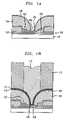
- FIG. 1Ashows a partially fabricated MOS HEMT device.
- the deviceincludes a substrate 101 and a multiple epilayer stack 102 , which includes a buried channel layer 103 .
- the layers of the epilayer stack 102may be grown using known growth methodologies; for example, metalorganic vapor phase epitaxy (MOVPE), also known as metalorganic chemical vapor deposition (MOCVD) and organometallic chemical vapor deposition (OMCVD), organometallic vapor phase epitaxy (OMVPE) and molecular beam epitaxy (MBE).
- MOVPEmetalorganic vapor phase epitaxy
- MOCVDmetalorganic chemical vapor deposition
- OMCVDorganometallic chemical vapor deposition
- MBEmolecular beam epitaxy
- a channel maskis formed (e.g., by patterned photoresist), and a recess 107 (often referred to as the first recess) is formed by a known etching sequence using the channel mask.
- a first gate mask 104(commonly referred to as the gate 1 mask) is disposed over the source and drain components including ohmic contacts thereof.
- the mask 104allows for etching of a recess 108 (often referred to as the second recess) in layer 109 , which is illustratively an undoped GaAs layer disposed over the buried channel 103 .
- the second recess etchmay provide the recess 108 through additional layers of the epilayer stack 102 .
- An oxide layer 105is formed over the first gate mask 104 , and over the recess 108 as shown.
- the oxide layer disposed over the recess 108provides a gate oxide 106 for the MOS HEMT.
- the oxide 105is illustratively an aluminum oxide (e.g., Al 2 O 3 ), which is deposited by a low-temperature (LT) atomic layer deposition (ALD) method.
- LTlow-temperature
- ALDatomic layer deposition
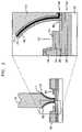
- FIG. 1Bshows the partially fabricated MOS HEMT after further processing.
- a barrier layer 110is formed over the oxide layer 105 and gate oxide 106 .
- the barrier layer 110is illustratively a refractory metal/refractory metal alloy useful in preventing migration of gate metal (e.g., Au) plated therover in a subsequent step into the underlying semiconductor.
- the barrier layer 110is Ti/TiW/TiWN/Ti, although other materials useful in preventing migration of metal/conductive material to the underlying semiconductor may be used.
- a seed layer 111is deposited over the barrier layer 110 .
- the fabrication sequenceis illustratively carried out in wafer-scale fabrication. As such, the seed layer 111 is provided over the entire wafer to foster electrochemical plating over the wafer as described herein.
- a second gate mask 112(commonly referred to as the gate 2 mask) is formed over the wafer, with openings above the first gate mask 104 and recess 108 to allow for the forming of the gate in a self-aligned manner.
- a gate 113is formed by a known electrochemical plating sequence, with the layer 111 functioning as a seed for the electrochemical plating over the wafer.
- the gate 113is gold; but may be another material(s) useful as a gate material and amenable to electrochemical plating.
- the fabrication of the gate 113 by electrochemical platingis beneficial compared to other methods of fabricating the gate, such as by known lift-off techniques.
- plated gatesprovide an improved gate cross section and thus more metal for lower gate resistance.
- processes of fabrication by electrochemical platingare often more readily adapted to large-scale manufacture; and may provide a gate with a comparably improved defect density.
- FIG. 1Cshows the partially fabricated MOS HEMT after further processing.
- the second gate mask 112is removed by standard technique.
- the seed layer 111 , the barrier layer 110 and the oxide layer 105must be removed all locations excepting beneath the gate 113 .
- the seed layer 111 and the barrier layer 110are removed from the first gate mask 104 .
- FIG. 1Dshows MOS HEMT essentially after final processing.
- the first gate mask 104is removed.
- the removal of the first gate mask 104reveals the first recess 107 and ohmic contacts 116 over the drain and source, and a nitride layer 115 thereover.
- the gate 113formed in a self-aligned manner over the recess 108 .
- removal of the first gate mask 104shows the (first) recess 107 , which is also aligned to the recess 108 and thus the gate 113 .
- a MOS HEMT structureis fabricated by a patterned plating technique and at comparatively low temperature processing.
- the resultant deviceusefully overcomes many of the shortcomings of other known devices; and its method of manufacture provides a substantially self-aligned gate structure device with insignificant modification to existing large-scale processing.
- FIG. 2is a cross-sectional view of a semiconductor device including an enlarged portion of the device in accordance with a representative embodiment.
- the deviceis substantially identical to the resultant device shown in FIG. 1D . As such, many details of the device are not repeated.
- the deviceincludes substrate 101 , and the epilayer stack 102 disposed thereover.
- the epilayer stack 102comprises a first layer of AlGaAs, a second layer of AlGaAs and an undoped layer of InGaAs, which forms the channel 103 .
- the materials of the representative embodimentsmay be others within the purview of one of ordinary skill in the art and may have a stoichiometry that is selected based on desired device characteristics among other considerations.
- the undoped layer 109which includes the recess 108 , is illustratively undoped GaAs.
- the gate oxide 106is formed over the recess 108 , with the portions of the barrier layer 110 and seed layer 111 formed over the gate oxide 106 .
- an ohmic cap layer 114is provided at the source and drain. This layer is usefully heavily doped and may be n + -doped GaAs.
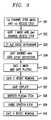
- FIG. 3is a flow diagram of a method of fabricating a semiconductor device in accordance with representative embodiment.
- the illustrative methodincludes many of the features and methods described in connection with representative embodiments described previously. As such, many details of the device are not repeated.
- MOS HEMT devices of representative embodimentsare illustratively double recess devices.
- the methodincludes forming a first channel etch mask and a first channel recess etch.
- a channel etch maskis formed, such as by patterned photoresist.
- Etchingis carried out by known methods to provide a recess in the upper layer(s) of the epilayer stack 102 , such as the cap layer 114 .
- the first gate mask 104is formed, such as by patterned photoresist. This mask is open over the undoped layer 109 , allowing for etching of this layer and other layers of the epilayer stack 102 over the buried channel layer 103 as desired.
- the LT ALD sequenceis effected.
- the depositionis effected at temperatures of less than 300 ° C.; and is beneficially effected at temperatures of in they range of approximately 25 ° C. to approximately 150° C. In certain embodiments, the deposition is effected at temperatures less than approximately 100° C.
- This LT ALD deposition thicknessmay range from approximately 20 Angstoms to approximately 300 Angstroms.
- the barrier layer 110(also referred to as the gate barrier) and seed layer 111 are formed in sequence via known methods.
- the barrier layer 110 and seed layer 111are sputter deposited by known methods to a combined thickness of approximately 1000 Angstroms.
- the second gate mask 112is formed.
- the mask 112is formed by patterned photoresist.
- the electrochemical plating sequenceis carried out to form gates 113 over the wafer and for each HEMT device thereon.
- the incorporation of electroplating in the fabrication sequence of illustrative embodimentsprovides significant benefits compared to other methods to form the gate, such as by lift-off methods.
- the second gate mask 112is removed.
- a flood expose/develop sequenceis effected and the resist is removed.
- the second gate mask 112may be removed through the use of solvent dissolution or through oxygen plasma cleaning.
- the seed layer 111is removed from above the first gate mask 104 by a reverse electrochemical plating sequence (also referred to as deplating).
- This deplating sequenceremoves the seed layer 111 across the wafer.
- the seed layerremains beneath the gate 113 as shown, for example, in FIG. 1C .
- the seed layer 111may be removed using a known chemical etch such as potassium iodide-iodine; or may be removed through ion bombardment using sputter etching or ion milling.
- the barrier layer 110is removed from above the first gate mask by a known plasma etching sequence. Again, as shown for example in FIG. 1C , the barrier layer 110 remains beneath the gate 113 .
- oxide layer 105is removed from the first gate mask 104 . The removal of the oxide 105 may be effected using a sputter etch, or other known plasma etch sequence. Notably, the oxide layer 105 , 106 remains beneath the gate 113 as shown in FIGS. 1D and 2 for example.
- the first gate mask 104is removed.
- the first gate maskis removed by known methods.
- the gate 113functions also as a mask, preventing damage to the underlying device.
- the resultant deviceis as shown in FIGS. 1D and 2 .
- MOS HEMT devices and methods of manufactureare described.
- One of ordinary skill in the artappreciates that many variations that are in accordance with the present teachings are possible and remain within the scope of the appended claims. These and other variations would become clear to one of ordinary skill in the art after inspection of the specification, drawings and claims herein. The invention therefore is not to be restricted except within the spirit and scope of the appended claims.
Landscapes
- Engineering & Computer Science (AREA)
- Physics & Mathematics (AREA)
- Condensed Matter Physics & Semiconductors (AREA)
- General Physics & Mathematics (AREA)
- Manufacturing & Machinery (AREA)
- Computer Hardware Design (AREA)
- Microelectronics & Electronic Packaging (AREA)
- Power Engineering (AREA)
- Junction Field-Effect Transistors (AREA)
Abstract
Description
- Gallium arsenide (GaAs) and other III-V alloys have exhibited great potential for high power and/or high frequency electronic applications. Particularly desirable applications include high electron mobility transistors (HEMTs), which are electronic devices having three terminals including a gate, a drain, and a source. The HEMT is a variant of GaAs field effect transistor (FET) technology that offers substantially better performance than standard metal-semiconductor field-effect transistor (MESFET) devices.
- A HEMT includes an undoped semiconductor (e.g., GaAs or an alloy thereof) channel with a thin doped layer of semiconductor (e.g., AlGaAs) between the channel and metal gate. The doped layer furnishes the carriers for the channel. Among other benefits, the electron mobility in the channel is higher in the HEMT than in a MESFET, because there are substantially no dopant ions in the channel to scatter carriers. This results in a two-dimensional electron gas (2 DEG, also referred to as the channel charge), which is formed along the heterointerface. Among other applications, GaAs based HEMTs have become the standard for signal amplification in civil and military radar, handset cellular, and satellite communications. GaAs has a higher electron mobility and a lower source resistance than Si, which allows GaAs based devices to function at higher frequencies.
- In many known HEMT devices, the gate forms a Schottky barrier with the semiconductor. Increasing the forward bias on the device increases the gate current, which in turn limits the voltage range of the device. In particular, increased gate current leads to a non-linear output and deleterious effects such as spurious frequencies. As will be appreciated, in many applications of HEMT devices, such as in communication devices, non-linear effects are undesirable.
- In an effort to reduce the gate current, application of an oxide layer between the gate metal and the semiconductor has been considered. While useful to this end, many known oxide deposition techniques are above accepted temperature tolerances in III-V semiconductor processing. For example, photoresists and device features such as alloyed contacts and organic spin-on dielectrics, are unable to withstand the temperatures required to provide many known oxides. This leads to certain shortcomings and undesired results. Among other deleterious effects, in fabricating double-recess HEMT devices by such a known method, the need to apply remove a first resist and apply a second resist to form the recess for the gate can result in misalignment of the gate over the channel.
- What is needed, therefore, is a method of fabricating III-V MOS devices that overcomes at least the shortcomings described.
- In accordance with an illustrative embodiment, a method of fabricating a semiconductor device includes forming a first gate mask; etching a recess in at least one semiconductor layer; atomic layer depositing an oxide layer; forming a second gate mask over the oxide layer; and plating a gate over the oxide layer.
- In accordance with another illustrative embodiment, a metal oxide semiconductor (MOS) transistor includes a Group III-V semiconductor substrate. The transistor also includes an oxide layer disposed over a channel and a plated gate disposed over the oxide layer. In addition, the transistor includes a seed layer disposed between the plated gate and the oxide layer.
- Representative embodiments are best understood from the following detailed description when read with the accompanying drawing figures. It is emphasized that the various features are not necessarily drawn to scale. In fact, the dimensions may be arbitrarily increased or decreased for clarity of discussion. Wherever applicable and practical, like reference numerals refer to like elements.
FIGS. 1A-1D are simplified cross-sectional views of a sequence for fabricating a semiconductor device in accordance with representative embodiment.FIG. 2 is a cross-sectional view of a semiconductor device including an enlarged portion of the device in accordance with a representative embodiment.FIG. 3 is a flow diagram of a method of fabricating a semiconductor device in accordance with representative embodiment.- The terms ‘a’ or ‘an’, as used herein are defined as one or more than one.
- The term ‘plurality’ as used herein is defined as two or more than two.
- In the following detailed description, for purposes of explanation and not limitation, specific details are set forth in order to provide a thorough understanding of example embodiments according to the present teachings. However, it will be apparent to one having ordinary skill in the art having had the benefit of the present disclosure that other embodiments according to the present teachings that depart from the specific details disclosed herein remain within the scope of the appended claims. Moreover, descriptions of apparati, devices, materials and methods known to one of ordinary skill in the art may be omitted so as to not obscure the description of the example embodiments. Such apparati, devices, methods and materials are clearly within the scope of the present teachings. Furthermore, although described with respect to a MOS HEMT device, the present teachings may be applied to other devices and structures. Generally, the present teachings may be applied to group III-V semiconductor devices and their fabrication.
FIGS. 1A-1D are simplified cross-sectional views of a sequence of fabricating a semiconductor device in accordance with representative embodiment. At the outset, it is emphasized that many of the materials and methods of fabrication of certain components of the resultant device are known to those skilled in the art. For example, illustrative methods and materials are described in: U.S. Patent Publication 20060102931 to Kopley, et al.; andFormation and Characterization of Nanometer Scale Metal-Oxide-Semiconductor Structures on GaAs Using Low-Temperature Atomic Layer Deposition, by P. D. Ye, et al. (Applied Physics Letters 87 013501-1,2,3 (2005)). The disclosure of this publication and paper are specifically incorporated herein by reference.FIG. 1A shows a partially fabricated MOS HEMT device. The device includes asubstrate 101 and amultiple epilayer stack 102, which includes a buriedchannel layer 103. The layers of theepilayer stack 102 may be grown using known growth methodologies; for example, metalorganic vapor phase epitaxy (MOVPE), also known as metalorganic chemical vapor deposition (MOCVD) and organometallic chemical vapor deposition (OMCVD), organometallic vapor phase epitaxy (OMVPE) and molecular beam epitaxy (MBE). Other growth methodologies are also possible.- In steps not shown, a channel mask is formed (e.g., by patterned photoresist), and a recess107 (often referred to as the first recess) is formed by a known etching sequence using the channel mask. Upon removal of the channel mask, and as shown in
FIG. 1A , a first gate mask104 (commonly referred to as thegate 1 mask) is disposed over the source and drain components including ohmic contacts thereof. Themask 104 allows for etching of a recess108 (often referred to as the second recess) inlayer 109, which is illustratively an undoped GaAs layer disposed over the buriedchannel 103. Notably, the second recess etch may provide therecess 108 through additional layers of theepilayer stack 102. - An
oxide layer 105 is formed over thefirst gate mask 104, and over therecess 108 as shown. The oxide layer disposed over therecess 108 provides agate oxide 106 for the MOS HEMT. As described more fully in conjunction with the representative embodiments ofFIG. 3 , theoxide 105 is illustratively an aluminum oxide (e.g., Al2O3), which is deposited by a low-temperature (LT) atomic layer deposition (ALD) method. An representative method is described in the referenced paper to Ye, et al. FIG. 1B shows the partially fabricated MOS HEMT after further processing. After depositing theoxide layer 105, abarrier layer 110 is formed over theoxide layer 105 andgate oxide 106. Thebarrier layer 110 is illustratively a refractory metal/refractory metal alloy useful in preventing migration of gate metal (e.g., Au) plated therover in a subsequent step into the underlying semiconductor. In a representative embodiment, thebarrier layer 110 is Ti/TiW/TiWN/Ti, although other materials useful in preventing migration of metal/conductive material to the underlying semiconductor may be used. After thebarrier layer 110 is deposited, aseed layer 111 is deposited over thebarrier layer 110. The fabrication sequence is illustratively carried out in wafer-scale fabrication. As such, theseed layer 111 is provided over the entire wafer to foster electrochemical plating over the wafer as described herein.- After the
seed layer 111 is formed, a second gate mask112 (commonly referred to as thegate 2 mask) is formed over the wafer, with openings above thefirst gate mask 104 andrecess 108 to allow for the forming of the gate in a self-aligned manner. After thesecond gate mask 112 is formed, agate 113 is formed by a known electrochemical plating sequence, with thelayer 111 functioning as a seed for the electrochemical plating over the wafer. In representative embodiments, thegate 113 is gold; but may be another material(s) useful as a gate material and amenable to electrochemical plating. - As will be appreciated by one of ordinary skill in the art, the fabrication of the
gate 113 by electrochemical plating is beneficial compared to other methods of fabricating the gate, such as by known lift-off techniques. For example, plated gates provide an improved gate cross section and thus more metal for lower gate resistance. In addition the processes of fabrication by electrochemical plating are often more readily adapted to large-scale manufacture; and may provide a gate with a comparably improved defect density. Thus, compared to known lift-off methods, there are many benefits to electrochemical plating of the representative embodiments, both in manufacturing and in the resultant product. FIG. 1C shows the partially fabricated MOS HEMT after further processing. Notably, after the forming of thegate 113, thesecond gate mask 112 is removed by standard technique. Next, theseed layer 111, thebarrier layer 110 and theoxide layer 105 must be removed all locations excepting beneath thegate 113. As such, theseed layer 111 and thebarrier layer 110 are removed from thefirst gate mask 104.FIG. 1D shows MOS HEMT essentially after final processing. After the removal of theseed layer 111, thebarrier layer 110 and thegate oxide layer 105 from all locations except beneath thegate 113, thefirst gate mask 104 is removed. The removal of thefirst gate mask 104 reveals thefirst recess 107 andohmic contacts 116 over the drain and source, and anitride layer 115 thereover. As such, thegate 113 formed in a self-aligned manner over therecess 108. Moreover, removal of thefirst gate mask 104 shows the (first)recess 107, which is also aligned to therecess 108 and thus thegate 113. Beneficially, in accordance with representative embodiments, a MOS HEMT structure is fabricated by a patterned plating technique and at comparatively low temperature processing. As will be appreciated by one of ordinary skill in the art, the resultant device usefully overcomes many of the shortcomings of other known devices; and its method of manufacture provides a substantially self-aligned gate structure device with insignificant modification to existing large-scale processing.FIG. 2 is a cross-sectional view of a semiconductor device including an enlarged portion of the device in accordance with a representative embodiment. The device is substantially identical to the resultant device shown inFIG. 1D . As such, many details of the device are not repeated.- The device includes
substrate 101, and theepilayer stack 102 disposed thereover. Illustratively, theepilayer stack 102 comprises a first layer of AlGaAs, a second layer of AlGaAs and an undoped layer of InGaAs, which forms thechannel 103. It is emphasized that the materials of the representative embodiments may be others within the purview of one of ordinary skill in the art and may have a stoichiometry that is selected based on desired device characteristics among other considerations. - The
undoped layer 109, which includes therecess 108, is illustratively undoped GaAs. Thegate oxide 106 is formed over therecess 108, with the portions of thebarrier layer 110 andseed layer 111 formed over thegate oxide 106. At the source and drain, anohmic cap layer 114 is provided. This layer is usefully heavily doped and may be n+-doped GaAs. FIG. 3 is a flow diagram of a method of fabricating a semiconductor device in accordance with representative embodiment. The illustrative method includes many of the features and methods described in connection with representative embodiments described previously. As such, many details of the device are not repeated.- As noted previously, MOS HEMT devices of representative embodiments are illustratively double recess devices. At
step 301, the method includes forming a first channel etch mask and a first channel recess etch. In this step, a channel etch mask is formed, such as by patterned photoresist. Etching is carried out by known methods to provide a recess in the upper layer(s) of theepilayer stack 102, such as thecap layer 114. - At
step 302, thefirst gate mask 104 is formed, such as by patterned photoresist. This mask is open over theundoped layer 109, allowing for etching of this layer and other layers of theepilayer stack 102 over the buriedchannel layer 103 as desired. - At
step 303, the LT ALD sequence is effected. In representative embodiments, the deposition is effected at temperatures of less than 300 ° C.; and is beneficially effected at temperatures of in they range of approximately 25 ° C. to approximately 150° C. In certain embodiments, the deposition is effected at temperatures less than approximately 100° C. This LT ALD deposition thickness may range from approximately 20 Angstoms to approximately 300 Angstroms. - At
step 304, the barrier layer110 (also referred to as the gate barrier) andseed layer 111 are formed in sequence via known methods. Illustratively, thebarrier layer 110 andseed layer 111 are sputter deposited by known methods to a combined thickness of approximately 1000 Angstroms. - At
step 305, thesecond gate mask 112 is formed. In a representative embodiments, themask 112 is formed by patterned photoresist. After thesecond gate mask 112 is patterned, the electrochemical plating sequence is carried out to formgates 113 over the wafer and for each HEMT device thereon. As noted previously, the incorporation of electroplating in the fabrication sequence of illustrative embodiments provides significant benefits compared to other methods to form the gate, such as by lift-off methods. - At
step 306, thesecond gate mask 112 is removed. In embodiments including a patterned resist for thesecond gate mask 112, a flood expose/develop sequence is effected and the resist is removed. Alternatively, thesecond gate mask 112 may be removed through the use of solvent dissolution or through oxygen plasma cleaning. - At
step 307, theseed layer 111 is removed from above thefirst gate mask 104 by a reverse electrochemical plating sequence (also referred to as deplating). This deplating sequence removes theseed layer 111 across the wafer. Notably, the seed layer remains beneath thegate 113 as shown, for example, inFIG. 1C . Alternatively, theseed layer 111 may be removed using a known chemical etch such as potassium iodide-iodine; or may be removed through ion bombardment using sputter etching or ion milling. - At
step 308, thebarrier layer 110 is removed from above the first gate mask by a known plasma etching sequence. Again, as shown for example inFIG. 1C , thebarrier layer 110 remains beneath thegate 113. Next, atstep 309,oxide layer 105 is removed from thefirst gate mask 104. The removal of theoxide 105 may be effected using a sputter etch, or other known plasma etch sequence. Notably, theoxide layer gate 113 as shown inFIGS. 1D and 2 for example. - At
step 310, thefirst gate mask 104 is removed. As in the removal of thesecond gate mask 112, the first gate mask is removed by known methods. Notably, duringsteps gate 113 functions also as a mask, preventing damage to the underlying device. At the termination ofstep 310, the resultant device is as shown inFIGS. 1D and 2 . - In connection with illustrative embodiments, MOS HEMT devices and methods of manufacture are described. One of ordinary skill in the art appreciates that many variations that are in accordance with the present teachings are possible and remain within the scope of the appended claims. These and other variations would become clear to one of ordinary skill in the art after inspection of the specification, drawings and claims herein. The invention therefore is not to be restricted except within the spirit and scope of the appended claims.
Claims (19)
Priority Applications (2)
| Application Number | Priority Date | Filing Date | Title |
|---|---|---|---|
| US11/749,459US8502272B2 (en) | 2007-05-16 | 2007-05-16 | Metal-oxide-semiconductor high electron mobility transistors and methods of fabrication |
| US13/930,332US8741705B2 (en) | 2007-05-16 | 2013-06-28 | Metal-oxide-semiconductor high electron mobility transistors and methods of fabrication |
Applications Claiming Priority (1)
| Application Number | Priority Date | Filing Date | Title |
|---|---|---|---|
| US11/749,459US8502272B2 (en) | 2007-05-16 | 2007-05-16 | Metal-oxide-semiconductor high electron mobility transistors and methods of fabrication |
Related Child Applications (1)
| Application Number | Title | Priority Date | Filing Date |
|---|---|---|---|
| US13/930,332DivisionUS8741705B2 (en) | 2007-05-16 | 2013-06-28 | Metal-oxide-semiconductor high electron mobility transistors and methods of fabrication |
Publications (2)
| Publication Number | Publication Date |
|---|---|
| US20080286915A1true US20080286915A1 (en) | 2008-11-20 |
| US8502272B2 US8502272B2 (en) | 2013-08-06 |
Family
ID=40027929
Family Applications (2)
| Application Number | Title | Priority Date | Filing Date |
|---|---|---|---|
| US11/749,459Active2030-07-11US8502272B2 (en) | 2007-05-16 | 2007-05-16 | Metal-oxide-semiconductor high electron mobility transistors and methods of fabrication |
| US13/930,332ActiveUS8741705B2 (en) | 2007-05-16 | 2013-06-28 | Metal-oxide-semiconductor high electron mobility transistors and methods of fabrication |
Family Applications After (1)
| Application Number | Title | Priority Date | Filing Date |
|---|---|---|---|
| US13/930,332ActiveUS8741705B2 (en) | 2007-05-16 | 2013-06-28 | Metal-oxide-semiconductor high electron mobility transistors and methods of fabrication |
Country Status (1)
| Country | Link |
|---|---|
| US (2) | US8502272B2 (en) |
Cited By (4)
| Publication number | Priority date | Publication date | Assignee | Title |
|---|---|---|---|---|
| US20110140169A1 (en)* | 2009-12-10 | 2011-06-16 | International Rectifier Corporation | Highly conductive source/drain contacts in III-nitride transistors |
| US20120302178A1 (en)* | 2011-05-25 | 2012-11-29 | Triquint Semiconductor, Inc. | Regrown shottky structures for gan hemt devices |
| US11367683B2 (en) | 2018-07-03 | 2022-06-21 | Infineon Technologies Ag | Silicon carbide device and method for forming a silicon carbide device |
| US11869840B2 (en) | 2018-07-03 | 2024-01-09 | Infineon Technologies Ag | Silicon carbide device and method for forming a silicon carbide device |
Citations (12)
| Publication number | Priority date | Publication date | Assignee | Title |
|---|---|---|---|---|
| US4923827A (en)* | 1988-05-16 | 1990-05-08 | Eaton Corporation | T-type undercut electrical contact process on a semiconductor substrate |
| US5300813A (en)* | 1992-02-26 | 1994-04-05 | International Business Machines Corporation | Refractory metal capped low resistivity metal conductor lines and vias |
| US5389574A (en)* | 1991-09-20 | 1995-02-14 | Sony Corporation | Selective etching method for III-V group semiconductor material using a mixed etching gas and a stop-etching gas |
| US5861327A (en)* | 1996-12-04 | 1999-01-19 | Electronics And Telecommunications Research Institute | Fabrication method of gate electrode in semiconductor device |
| US6146931A (en)* | 1997-12-02 | 2000-11-14 | Fujitsu Quantum Devices Limited | Method of forming a semiconductor device having a barrier layer interposed between the ohmic contact and the schottky contact |
| US6410418B1 (en)* | 1999-08-18 | 2002-06-25 | Advanced Micro Devices, Inc. | Recess metallization via selective insulator formation on nucleation/seed layer |
| US6521961B1 (en)* | 2000-04-28 | 2003-02-18 | Motorola, Inc. | Semiconductor device using a barrier layer between the gate electrode and substrate and method therefor |
| US20030213975A1 (en)* | 2002-05-17 | 2003-11-20 | Matsushita Electric Industrial Co, Ltd. | Semiconductor device |
| US20040056366A1 (en)* | 2002-09-25 | 2004-03-25 | Maiz Jose A. | A method of forming surface alteration of metal interconnect in integrated circuits for electromigration and adhesion improvement |
| US20050139868A1 (en)* | 2003-12-24 | 2005-06-30 | Matsushita Electric Industrial Co., Ltd. | Field effect transistor and method of manufacturing the same |
| US20080258176A1 (en)* | 2007-04-18 | 2008-10-23 | Yeong-Chang Chou | Antimonide-based compound semiconductor with titanium tungsten stack |
| US7847410B2 (en)* | 2005-08-22 | 2010-12-07 | National Chiao Tung University | Interconnect of group III-V semiconductor device and fabrication method for making the same |
Family Cites Families (1)
| Publication number | Priority date | Publication date | Assignee | Title |
|---|---|---|---|---|
| DE102006012369A1 (en)* | 2006-03-17 | 2007-09-20 | United Monolithic Semiconductors Gmbh | Method for producing a semiconductor component with a metallic control electrode and semiconductor component |
- 2007
- 2007-05-16USUS11/749,459patent/US8502272B2/enactiveActive
- 2013
- 2013-06-28USUS13/930,332patent/US8741705B2/enactiveActive
Patent Citations (12)
| Publication number | Priority date | Publication date | Assignee | Title |
|---|---|---|---|---|
| US4923827A (en)* | 1988-05-16 | 1990-05-08 | Eaton Corporation | T-type undercut electrical contact process on a semiconductor substrate |
| US5389574A (en)* | 1991-09-20 | 1995-02-14 | Sony Corporation | Selective etching method for III-V group semiconductor material using a mixed etching gas and a stop-etching gas |
| US5300813A (en)* | 1992-02-26 | 1994-04-05 | International Business Machines Corporation | Refractory metal capped low resistivity metal conductor lines and vias |
| US5861327A (en)* | 1996-12-04 | 1999-01-19 | Electronics And Telecommunications Research Institute | Fabrication method of gate electrode in semiconductor device |
| US6146931A (en)* | 1997-12-02 | 2000-11-14 | Fujitsu Quantum Devices Limited | Method of forming a semiconductor device having a barrier layer interposed between the ohmic contact and the schottky contact |
| US6410418B1 (en)* | 1999-08-18 | 2002-06-25 | Advanced Micro Devices, Inc. | Recess metallization via selective insulator formation on nucleation/seed layer |
| US6521961B1 (en)* | 2000-04-28 | 2003-02-18 | Motorola, Inc. | Semiconductor device using a barrier layer between the gate electrode and substrate and method therefor |
| US20030213975A1 (en)* | 2002-05-17 | 2003-11-20 | Matsushita Electric Industrial Co, Ltd. | Semiconductor device |
| US20040056366A1 (en)* | 2002-09-25 | 2004-03-25 | Maiz Jose A. | A method of forming surface alteration of metal interconnect in integrated circuits for electromigration and adhesion improvement |
| US20050139868A1 (en)* | 2003-12-24 | 2005-06-30 | Matsushita Electric Industrial Co., Ltd. | Field effect transistor and method of manufacturing the same |
| US7847410B2 (en)* | 2005-08-22 | 2010-12-07 | National Chiao Tung University | Interconnect of group III-V semiconductor device and fabrication method for making the same |
| US20080258176A1 (en)* | 2007-04-18 | 2008-10-23 | Yeong-Chang Chou | Antimonide-based compound semiconductor with titanium tungsten stack |
Cited By (7)
| Publication number | Priority date | Publication date | Assignee | Title |
|---|---|---|---|---|
| US20110140169A1 (en)* | 2009-12-10 | 2011-06-16 | International Rectifier Corporation | Highly conductive source/drain contacts in III-nitride transistors |
| EP2333823A3 (en)* | 2009-12-10 | 2011-12-28 | International Rectifier Corporation | Highly conductive source/drain contacts in lll- nitride transistors |
| US9378965B2 (en) | 2009-12-10 | 2016-06-28 | Infineon Technologies Americas Corp. | Highly conductive source/drain contacts in III-nitride transistors |
| US20120302178A1 (en)* | 2011-05-25 | 2012-11-29 | Triquint Semiconductor, Inc. | Regrown shottky structures for gan hemt devices |
| US8778747B2 (en)* | 2011-05-25 | 2014-07-15 | Triquint Semiconductor, Inc. | Regrown Schottky structures for GAN HEMT devices |
| US11367683B2 (en) | 2018-07-03 | 2022-06-21 | Infineon Technologies Ag | Silicon carbide device and method for forming a silicon carbide device |
| US11869840B2 (en) | 2018-07-03 | 2024-01-09 | Infineon Technologies Ag | Silicon carbide device and method for forming a silicon carbide device |
Also Published As
| Publication number | Publication date |
|---|---|
| US8741705B2 (en) | 2014-06-03 |
| US8502272B2 (en) | 2013-08-06 |
| US20130288461A1 (en) | 2013-10-31 |
Similar Documents
| Publication | Publication Date | Title |
|---|---|---|
| US7470941B2 (en) | High power-low noise microwave GaN heterojunction field effect transistor | |
| US6586781B2 (en) | Group III nitride based FETs and HEMTs with reduced trapping and method for producing the same | |
| US10014402B1 (en) | High electron mobility transistor (HEMT) device structure | |
| US9508807B2 (en) | Method of forming high electron mobility transistor | |
| JP5203220B2 (en) | Method of making a transistor with a supported gate electrode and associated device | |
| US7592211B2 (en) | Methods of fabricating transistors including supported gate electrodes | |
| JP7677742B2 (en) | Enhancement-mode metal-insulator-semiconductor high electron mobility transistor | |
| EP2246880B1 (en) | Semiconductor device fabrication method | |
| US9123645B2 (en) | Methods of making semiconductor devices with low leakage Schottky contacts | |
| US7160766B2 (en) | Field-effect semiconductor device and method for making the same | |
| US11508839B2 (en) | High electron mobility transistor with trench isolation structure capable of applying stress and method of manufacturing the same | |
| WO2009012536A1 (en) | Damascene contacts on iii-v cmos devices | |
| US9385001B1 (en) | Self-aligned ITO gate electrode for GaN HEMT device | |
| US8741705B2 (en) | Metal-oxide-semiconductor high electron mobility transistors and methods of fabrication | |
| US11955522B2 (en) | Semiconductor structure and method of forming the same | |
| US20130146885A1 (en) | Vertical GaN-Based Metal Insulator Semiconductor FET | |
| Yoon et al. | Wide head T-shaped gate process for low-noise AlGaN/GaN HEMTs | |
| CN112219283A (en) | Semiconductor device and method for manufacturing the same | |
| EP4590085A1 (en) | Improved depletion mode hemt device and manufacturing process thereof | |
| CN120358770A (en) | Improved HEMT device, in particular depletion mode device, and process for manufacturing same | |
| CN112909089A (en) | Semiconductor structure and forming method thereof | |
| JPS62213173A (en) | Manufacturing method of semiconductor device | |
| JPH0492440A (en) | Method for manufacturing semiconductor integrated circuit device |
Legal Events
| Date | Code | Title | Description |
|---|---|---|---|
| AS | Assignment | Owner name:AVAGO TECHNOLOGIES WIRELESS IP (SINGAPORE) PTE. LT Free format text:ASSIGNMENT OF ASSIGNORS INTEREST;ASSIGNORS:DUNGAN, THOMAS EDWARD;NIKKEL, PHILIP GENE;REEL/FRAME:021259/0519;SIGNING DATES FROM 20080514 TO 20080515 Owner name:AVAGO TECHNOLOGIES WIRELESS IP (SINGAPORE) PTE. LT Free format text:ASSIGNMENT OF ASSIGNORS INTEREST;ASSIGNORS:DUNGAN, THOMAS EDWARD;NIKKEL, PHILIP GENE;SIGNING DATES FROM 20080514 TO 20080515;REEL/FRAME:021259/0519 | |
| AS | Assignment | Owner name:AVAGO TECHNOLOGIES GENERAL IP (SINGAPORE) PTE. LTD Free format text:MERGER;ASSIGNOR:AVAGO TECHNOLOGIES WIRELESS IP (SINGAPORE) PTE. LTD.;REEL/FRAME:030331/0632 Effective date:20121030 | |
| STCF | Information on status: patent grant | Free format text:PATENTED CASE | |
| AS | Assignment | Owner name:DEUTSCHE BANK AG NEW YORK BRANCH, AS COLLATERAL AGENT, NEW YORK Free format text:PATENT SECURITY AGREEMENT;ASSIGNOR:AVAGO TECHNOLOGIES GENERAL IP (SINGAPORE) PTE. LTD.;REEL/FRAME:032851/0001 Effective date:20140506 Owner name:DEUTSCHE BANK AG NEW YORK BRANCH, AS COLLATERAL AG Free format text:PATENT SECURITY AGREEMENT;ASSIGNOR:AVAGO TECHNOLOGIES GENERAL IP (SINGAPORE) PTE. LTD.;REEL/FRAME:032851/0001 Effective date:20140506 | |
| AS | Assignment | Owner name:AVAGO TECHNOLOGIES GENERAL IP (SINGAPORE) PTE. LTD., SINGAPORE Free format text:TERMINATION AND RELEASE OF SECURITY INTEREST IN PATENT RIGHTS (RELEASES RF 032851-0001);ASSIGNOR:DEUTSCHE BANK AG NEW YORK BRANCH, AS COLLATERAL AGENT;REEL/FRAME:037689/0001 Effective date:20160201 Owner name:AVAGO TECHNOLOGIES GENERAL IP (SINGAPORE) PTE. LTD Free format text:TERMINATION AND RELEASE OF SECURITY INTEREST IN PATENT RIGHTS (RELEASES RF 032851-0001);ASSIGNOR:DEUTSCHE BANK AG NEW YORK BRANCH, AS COLLATERAL AGENT;REEL/FRAME:037689/0001 Effective date:20160201 | |
| AS | Assignment | Owner name:BANK OF AMERICA, N.A., AS COLLATERAL AGENT, NORTH CAROLINA Free format text:PATENT SECURITY AGREEMENT;ASSIGNOR:AVAGO TECHNOLOGIES GENERAL IP (SINGAPORE) PTE. LTD.;REEL/FRAME:037808/0001 Effective date:20160201 Owner name:BANK OF AMERICA, N.A., AS COLLATERAL AGENT, NORTH Free format text:PATENT SECURITY AGREEMENT;ASSIGNOR:AVAGO TECHNOLOGIES GENERAL IP (SINGAPORE) PTE. LTD.;REEL/FRAME:037808/0001 Effective date:20160201 | |
| FPAY | Fee payment | Year of fee payment:4 | |
| AS | Assignment | Owner name:AVAGO TECHNOLOGIES GENERAL IP (SINGAPORE) PTE. LTD., SINGAPORE Free format text:TERMINATION AND RELEASE OF SECURITY INTEREST IN PATENTS;ASSIGNOR:BANK OF AMERICA, N.A., AS COLLATERAL AGENT;REEL/FRAME:041710/0001 Effective date:20170119 Owner name:AVAGO TECHNOLOGIES GENERAL IP (SINGAPORE) PTE. LTD Free format text:TERMINATION AND RELEASE OF SECURITY INTEREST IN PATENTS;ASSIGNOR:BANK OF AMERICA, N.A., AS COLLATERAL AGENT;REEL/FRAME:041710/0001 Effective date:20170119 | |
| AS | Assignment | Owner name:AVAGO TECHNOLOGIES INTERNATIONAL SALES PTE. LIMITE Free format text:MERGER;ASSIGNOR:AVAGO TECHNOLOGIES GENERAL IP (SINGAPORE) PTE. LTD.;REEL/FRAME:047230/0910 Effective date:20180509 | |
| AS | Assignment | Owner name:AVAGO TECHNOLOGIES INTERNATIONAL SALES PTE. LIMITE Free format text:CORRECTIVE ASSIGNMENT TO CORRECT THE EFFECTIVE DATE OF THE MERGER PREVIOUSLY RECORDED AT REEL: 047230 FRAME: 0910. ASSIGNOR(S) HEREBY CONFIRMS THE MERGER;ASSIGNOR:AVAGO TECHNOLOGIES GENERAL IP (SINGAPORE) PTE. LTD.;REEL/FRAME:047351/0384 Effective date:20180905 | |
| AS | Assignment | Owner name:AVAGO TECHNOLOGIES INTERNATIONAL SALES PTE. LIMITE Free format text:CORRECTIVE ASSIGNMENT TO CORRECT THE ERROR IN RECORDING THE MERGER IN THE INCORRECT US PATENT NO. 8,876,094 PREVIOUSLY RECORDED ON REEL 047351 FRAME 0384. ASSIGNOR(S) HEREBY CONFIRMS THE MERGER;ASSIGNOR:AVAGO TECHNOLOGIES GENERAL IP (SINGAPORE) PTE. LTD.;REEL/FRAME:049248/0558 Effective date:20180905 | |
| MAFP | Maintenance fee payment | Free format text:PAYMENT OF MAINTENANCE FEE, 8TH YEAR, LARGE ENTITY (ORIGINAL EVENT CODE: M1552); ENTITY STATUS OF PATENT OWNER: LARGE ENTITY Year of fee payment:8 | |
| MAFP | Maintenance fee payment | Free format text:PAYMENT OF MAINTENANCE FEE, 12TH YEAR, LARGE ENTITY (ORIGINAL EVENT CODE: M1553); ENTITY STATUS OF PATENT OWNER: LARGE ENTITY Year of fee payment:12 |