US20080286659A1 - Extensions of Self-Assembled Structures to Increased Dimensions via a "Bootstrap" Self-Templating Method - Google Patents
Extensions of Self-Assembled Structures to Increased Dimensions via a "Bootstrap" Self-Templating MethodDownload PDFInfo
- Publication number
- US20080286659A1 US20080286659A1US11/738,169US73816907AUS2008286659A1US 20080286659 A1US20080286659 A1US 20080286659A1US 73816907 AUS73816907 AUS 73816907AUS 2008286659 A1US2008286659 A1US 2008286659A1
- Authority
- US
- United States
- Prior art keywords
- film
- trench
- polymer
- self
- domains
- Prior art date
- Legal status (The legal status is an assumption and is not a legal conclusion. Google has not performed a legal analysis and makes no representation as to the accuracy of the status listed.)
- Granted
Links
- 238000000034methodMethods0.000titleclaimsabstractdescription59
- 229920001400block copolymerPolymers0.000claimsabstractdescription112
- 229920000642polymerPolymers0.000claimsdescription160
- 239000000758substrateSubstances0.000claimsdescription91
- 238000009736wettingMethods0.000claimsdescription64
- 239000011159matrix materialSubstances0.000claimsdescription49
- 238000000137annealingMethods0.000claimsdescription47
- 230000007935neutral effectEffects0.000claimsdescription33
- 238000004132cross linkingMethods0.000claimsdescription20
- 238000005530etchingMethods0.000claimsdescription5
- 238000000926separation methodMethods0.000claimsdescription3
- 239000000463materialSubstances0.000abstractdescription92
- 238000003491arrayMethods0.000abstractdescription6
- 239000002086nanomaterialSubstances0.000abstractdescription5
- 239000010408filmSubstances0.000description130
- 239000010410layerSubstances0.000description93
- 229920003229poly(methyl methacrylate)Polymers0.000description66
- 239000004926polymethyl methacrylateSubstances0.000description66
- 229920001577copolymerPolymers0.000description44
- 239000004793PolystyreneSubstances0.000description40
- 229920000359diblock copolymerPolymers0.000description30
- 239000011295pitchSubstances0.000description26
- 125000006850spacer groupChemical group0.000description21
- VYPSYNLAJGMNEJ-UHFFFAOYSA-NSilicium dioxideChemical compoundO=[Si]=OVYPSYNLAJGMNEJ-UHFFFAOYSA-N0.000description19
- 229910052710siliconInorganic materials0.000description19
- XUIMIQQOPSSXEZ-UHFFFAOYSA-NSiliconChemical compound[Si]XUIMIQQOPSSXEZ-UHFFFAOYSA-N0.000description18
- 239000010703siliconSubstances0.000description18
- 239000000203mixtureSubstances0.000description17
- 229910052814silicon oxideInorganic materials0.000description15
- 239000010409thin filmSubstances0.000description11
- 239000002356single layerSubstances0.000description10
- YXFVVABEGXRONW-UHFFFAOYSA-NTolueneChemical compoundCC1=CC=CC=C1YXFVVABEGXRONW-UHFFFAOYSA-N0.000description9
- 229920005604random copolymerPolymers0.000description9
- 229920001519homopolymerPolymers0.000description8
- 239000002904solventSubstances0.000description8
- 238000004528spin coatingMethods0.000description8
- 238000004519manufacturing processMethods0.000description7
- 239000002184metalSubstances0.000description6
- 229910052751metalInorganic materials0.000description6
- 238000000206photolithographyMethods0.000description6
- 239000002861polymer materialSubstances0.000description6
- 239000004065semiconductorSubstances0.000description6
- 235000012431wafersNutrition0.000description6
- 239000003989dielectric materialSubstances0.000description5
- 238000000059patterningMethods0.000description5
- 239000000243solutionSubstances0.000description5
- 230000015572biosynthetic processEffects0.000description4
- 125000002887hydroxy groupChemical group[H]O*0.000description4
- 230000001939inductive effectEffects0.000description4
- 238000001338self-assemblyMethods0.000description4
- KRHYYFGTRYWZRS-UHFFFAOYSA-NFluoraneChemical compoundFKRHYYFGTRYWZRS-UHFFFAOYSA-N0.000description3
- CERQOIWHTDAKMF-UHFFFAOYSA-MMethacrylateChemical compoundCC(=C)C([O-])=OCERQOIWHTDAKMF-UHFFFAOYSA-M0.000description3
- 229910052581Si3N4Inorganic materials0.000description3
- 239000003990capacitorSubstances0.000description3
- 229920006037cross link polymerPolymers0.000description3
- 239000003431cross linking reagentSubstances0.000description3
- 238000000151depositionMethods0.000description3
- 239000012634fragmentSubstances0.000description3
- 230000000737periodic effectEffects0.000description3
- 238000009832plasma treatmentMethods0.000description3
- 230000005855radiationEffects0.000description3
- HQVNEWCFYHHQES-UHFFFAOYSA-Nsilicon nitrideChemical compoundN12[Si]34N5[Si]62N3[Si]51N64HQVNEWCFYHHQES-UHFFFAOYSA-N0.000description3
- 229920002818(Hydroxyethyl)methacrylatePolymers0.000description2
- MYRTYDVEIRVNKP-UHFFFAOYSA-N1,2-DivinylbenzeneChemical compoundC=CC1=CC=CC=C1C=CMYRTYDVEIRVNKP-UHFFFAOYSA-N0.000description2
- WOBHKFSMXKNTIM-UHFFFAOYSA-NHydroxyethyl methacrylateChemical compoundCC(=C)C(=O)OCCOWOBHKFSMXKNTIM-UHFFFAOYSA-N0.000description2
- 229920000390Poly(styrene-block-methyl methacrylate)Polymers0.000description2
- 239000005062PolybutadieneSubstances0.000description2
- PPBRXRYQALVLMV-UHFFFAOYSA-NStyreneChemical compoundC=CC1=CC=CC=C1PPBRXRYQALVLMV-UHFFFAOYSA-N0.000description2
- MCMNRKCIXSYSNV-UHFFFAOYSA-NZirconium dioxideChemical compoundO=[Zr]=OMCMNRKCIXSYSNV-UHFFFAOYSA-N0.000description2
- 239000000956alloySubstances0.000description2
- 229910045601alloyInorganic materials0.000description2
- 238000000429assemblyMethods0.000description2
- 230000000712assemblyEffects0.000description2
- 238000004630atomic force microscopyMethods0.000description2
- QVGXLLKOCUKJST-UHFFFAOYSA-Natomic oxygenChemical compound[O]QVGXLLKOCUKJST-UHFFFAOYSA-N0.000description2
- 229920005601base polymerPolymers0.000description2
- 229910052681coesiteInorganic materials0.000description2
- 239000000470constituentSubstances0.000description2
- 229910052906cristobaliteInorganic materials0.000description2
- 238000010894electron beam technologyMethods0.000description2
- 230000009477glass transitionEffects0.000description2
- 229910000040hydrogen fluorideInorganic materials0.000description2
- 238000011065in-situ storageMethods0.000description2
- 229920006030multiblock copolymerPolymers0.000description2
- 239000002070nanowireSubstances0.000description2
- 239000003960organic solventSubstances0.000description2
- 239000001301oxygenSubstances0.000description2
- 229910052760oxygenInorganic materials0.000description2
- -1poly(methylmethacrylate)Polymers0.000description2
- 229920002857polybutadienePolymers0.000description2
- 229920001195polyisoprenePolymers0.000description2
- 229920002223polystyrenePolymers0.000description2
- 229920002717polyvinylpyridinePolymers0.000description2
- 239000000377silicon dioxideSubstances0.000description2
- 229910052682stishoviteInorganic materials0.000description2
- 229920000428triblock copolymerPolymers0.000description2
- 229910052905tridymiteInorganic materials0.000description2
- SCYULBFZEHDVBN-UHFFFAOYSA-N1,1-DichloroethaneChemical compoundCC(Cl)ClSCYULBFZEHDVBN-UHFFFAOYSA-N0.000description1
- DDFHBQSCUXNBSA-UHFFFAOYSA-N5-(5-carboxythiophen-2-yl)thiophene-2-carboxylic acidChemical compoundS1C(C(=O)O)=CC=C1C1=CC=C(C(O)=O)S1DDFHBQSCUXNBSA-UHFFFAOYSA-N0.000description1
- KRHYYFGTRYWZRS-UHFFFAOYSA-MFluoride anionChemical compound[F-]KRHYYFGTRYWZRS-UHFFFAOYSA-M0.000description1
- UFHFLCQGNIYNRP-UHFFFAOYSA-NHydrogenChemical compound[H][H]UFHFLCQGNIYNRP-UHFFFAOYSA-N0.000description1
- YZCKVEUIGOORGS-UHFFFAOYSA-NHydrogen atomChemical compound[H]YZCKVEUIGOORGS-UHFFFAOYSA-N0.000description1
- VVQNEPGJFQJSBK-UHFFFAOYSA-NMethyl methacrylateChemical compoundCOC(=O)C(C)=CVVQNEPGJFQJSBK-UHFFFAOYSA-N0.000description1
- 206010040736Sinoatrial blockDiseases0.000description1
- 229910002370SrTiO3Inorganic materials0.000description1
- 230000006978adaptationEffects0.000description1
- 229910052782aluminiumInorganic materials0.000description1
- PNEYBMLMFCGWSK-UHFFFAOYSA-Naluminium oxideInorganic materials[O-2].[O-2].[O-2].[Al+3].[Al+3]PNEYBMLMFCGWSK-UHFFFAOYSA-N0.000description1
- LDDQLRUQCUTJBB-UHFFFAOYSA-Nammonium fluorideChemical compound[NH4+].[F-]LDDQLRUQCUTJBB-UHFFFAOYSA-N0.000description1
- 239000007864aqueous solutionSubstances0.000description1
- 238000005266castingMethods0.000description1
- 239000004020conductorSubstances0.000description1
- 238000010276constructionMethods0.000description1
- 229910052802copperInorganic materials0.000description1
- 229910052593corundumInorganic materials0.000description1
- 230000008021depositionEffects0.000description1
- 238000000609electron-beam lithographyMethods0.000description1
- 238000000572ellipsometryMethods0.000description1
- 238000001704evaporationMethods0.000description1
- 238000001900extreme ultraviolet lithographyMethods0.000description1
- 230000005669field effectEffects0.000description1
- 238000009472formulationMethods0.000description1
- PCHJSUWPFVWCPO-UHFFFAOYSA-NgoldChemical compound[Au]PCHJSUWPFVWCPO-UHFFFAOYSA-N0.000description1
- 239000010931goldSubstances0.000description1
- 229910052737goldInorganic materials0.000description1
- CJNBYAVZURUTKZ-UHFFFAOYSA-Nhafnium(IV) oxideInorganic materialsO=[Hf]=OCJNBYAVZURUTKZ-UHFFFAOYSA-N0.000description1
- 238000010438heat treatmentMethods0.000description1
- 239000001257hydrogenSubstances0.000description1
- 229910052739hydrogenInorganic materials0.000description1
- 238000007654immersionMethods0.000description1
- 239000011810insulating materialSubstances0.000description1
- 238000001459lithographyMethods0.000description1
- 125000002496methyl groupChemical group[H]C([H])([H])*0.000description1
- 239000000178monomerSubstances0.000description1
- 230000003287optical effectEffects0.000description1
- 229920002120photoresistant polymerPolymers0.000description1
- 229920006254polymer filmPolymers0.000description1
- 238000003672processing methodMethods0.000description1
- 238000010526radical polymerization reactionMethods0.000description1
- 238000004626scanning electron microscopyMethods0.000description1
- 239000000126substanceSubstances0.000description1
- 230000008961swellingEffects0.000description1
- 238000012876topographyMethods0.000description1
- 238000004627transmission electron microscopyMethods0.000description1
- 229910052721tungstenInorganic materials0.000description1
- 229910001845yogo sapphireInorganic materials0.000description1
Images


Classifications
- B—PERFORMING OPERATIONS; TRANSPORTING
- B81—MICROSTRUCTURAL TECHNOLOGY
- B81C—PROCESSES OR APPARATUS SPECIALLY ADAPTED FOR THE MANUFACTURE OR TREATMENT OF MICROSTRUCTURAL DEVICES OR SYSTEMS
- B81C99/00—Subject matter not provided for in other groups of this subclass
- H—ELECTRICITY
- H01—ELECTRIC ELEMENTS
- H01L—SEMICONDUCTOR DEVICES NOT COVERED BY CLASS H10
- H01L21/00—Processes or apparatus adapted for the manufacture or treatment of semiconductor or solid state devices or of parts thereof
- H01L21/02—Manufacture or treatment of semiconductor devices or of parts thereof
- H01L21/04—Manufacture or treatment of semiconductor devices or of parts thereof the devices having potential barriers, e.g. a PN junction, depletion layer or carrier concentration layer
- H01L21/18—Manufacture or treatment of semiconductor devices or of parts thereof the devices having potential barriers, e.g. a PN junction, depletion layer or carrier concentration layer the devices having semiconductor bodies comprising elements of Group IV of the Periodic Table or AIIIBV compounds with or without impurities, e.g. doping materials
- H01L21/30—Treatment of semiconductor bodies using processes or apparatus not provided for in groups H01L21/20 - H01L21/26
- H01L21/302—Treatment of semiconductor bodies using processes or apparatus not provided for in groups H01L21/20 - H01L21/26 to change their surface-physical characteristics or shape, e.g. etching, polishing, cutting
- H01L21/306—Chemical or electrical treatment, e.g. electrolytic etching
- H01L21/308—Chemical or electrical treatment, e.g. electrolytic etching using masks
- H01L21/3083—Chemical or electrical treatment, e.g. electrolytic etching using masks characterised by their size, orientation, disposition, behaviour, shape, in horizontal or vertical plane
- H01L21/3086—Chemical or electrical treatment, e.g. electrolytic etching using masks characterised by their size, orientation, disposition, behaviour, shape, in horizontal or vertical plane characterised by the process involved to create the mask, e.g. lift-off masks, sidewalls, or to modify the mask, e.g. pre-treatment, post-treatment
- B—PERFORMING OPERATIONS; TRANSPORTING
- B81—MICROSTRUCTURAL TECHNOLOGY
- B81C—PROCESSES OR APPARATUS SPECIALLY ADAPTED FOR THE MANUFACTURE OR TREATMENT OF MICROSTRUCTURAL DEVICES OR SYSTEMS
- B81C1/00—Manufacture or treatment of devices or systems in or on a substrate
- B—PERFORMING OPERATIONS; TRANSPORTING
- B81—MICROSTRUCTURAL TECHNOLOGY
- B81C—PROCESSES OR APPARATUS SPECIALLY ADAPTED FOR THE MANUFACTURE OR TREATMENT OF MICROSTRUCTURAL DEVICES OR SYSTEMS
- B81C1/00—Manufacture or treatment of devices or systems in or on a substrate
- B81C1/00015—Manufacture or treatment of devices or systems in or on a substrate for manufacturing microsystems
- B81C1/00023—Manufacture or treatment of devices or systems in or on a substrate for manufacturing microsystems without movable or flexible elements
- B81C1/00031—Regular or irregular arrays of nanoscale structures, e.g. etch mask layer
- B—PERFORMING OPERATIONS; TRANSPORTING
- B82—NANOTECHNOLOGY
- B82Y—SPECIFIC USES OR APPLICATIONS OF NANOSTRUCTURES; MEASUREMENT OR ANALYSIS OF NANOSTRUCTURES; MANUFACTURE OR TREATMENT OF NANOSTRUCTURES
- B82Y10/00—Nanotechnology for information processing, storage or transmission, e.g. quantum computing or single electron logic
- B—PERFORMING OPERATIONS; TRANSPORTING
- B82—NANOTECHNOLOGY
- B82Y—SPECIFIC USES OR APPLICATIONS OF NANOSTRUCTURES; MEASUREMENT OR ANALYSIS OF NANOSTRUCTURES; MANUFACTURE OR TREATMENT OF NANOSTRUCTURES
- B82Y40/00—Manufacture or treatment of nanostructures
- G—PHYSICS
- G03—PHOTOGRAPHY; CINEMATOGRAPHY; ANALOGOUS TECHNIQUES USING WAVES OTHER THAN OPTICAL WAVES; ELECTROGRAPHY; HOLOGRAPHY
- G03F—PHOTOMECHANICAL PRODUCTION OF TEXTURED OR PATTERNED SURFACES, e.g. FOR PRINTING, FOR PROCESSING OF SEMICONDUCTOR DEVICES; MATERIALS THEREFOR; ORIGINALS THEREFOR; APPARATUS SPECIALLY ADAPTED THEREFOR
- G03F7/00—Photomechanical, e.g. photolithographic, production of textured or patterned surfaces, e.g. printing surfaces; Materials therefor, e.g. comprising photoresists; Apparatus specially adapted therefor
- G03F7/0002—Lithographic processes using patterning methods other than those involving the exposure to radiation, e.g. by stamping
- H—ELECTRICITY
- H01—ELECTRIC ELEMENTS
- H01L—SEMICONDUCTOR DEVICES NOT COVERED BY CLASS H10
- H01L21/00—Processes or apparatus adapted for the manufacture or treatment of semiconductor or solid state devices or of parts thereof
- H01L21/02—Manufacture or treatment of semiconductor devices or of parts thereof
- H01L21/027—Making masks on semiconductor bodies for further photolithographic processing not provided for in group H01L21/18 or H01L21/34
- H01L21/033—Making masks on semiconductor bodies for further photolithographic processing not provided for in group H01L21/18 or H01L21/34 comprising inorganic layers
- H01L21/0334—Making masks on semiconductor bodies for further photolithographic processing not provided for in group H01L21/18 or H01L21/34 comprising inorganic layers characterised by their size, orientation, disposition, behaviour, shape, in horizontal or vertical plane
- H01L21/0337—Making masks on semiconductor bodies for further photolithographic processing not provided for in group H01L21/18 or H01L21/34 comprising inorganic layers characterised by their size, orientation, disposition, behaviour, shape, in horizontal or vertical plane characterised by the process involved to create the mask, e.g. lift-off masks, sidewalls, or to modify the mask, e.g. pre-treatment, post-treatment
- H—ELECTRICITY
- H01—ELECTRIC ELEMENTS
- H01L—SEMICONDUCTOR DEVICES NOT COVERED BY CLASS H10
- H01L21/00—Processes or apparatus adapted for the manufacture or treatment of semiconductor or solid state devices or of parts thereof
- H01L21/70—Manufacture or treatment of devices consisting of a plurality of solid state components formed in or on a common substrate or of parts thereof; Manufacture of integrated circuit devices or of parts thereof
- H01L21/71—Manufacture of specific parts of devices defined in group H01L21/70
- H01L21/768—Applying interconnections to be used for carrying current between separate components within a device comprising conductors and dielectrics
- H01L21/76838—Applying interconnections to be used for carrying current between separate components within a device comprising conductors and dielectrics characterised by the formation and the after-treatment of the conductors
- H01L21/76877—Filling of holes, grooves or trenches, e.g. vias, with conductive material
- H01L21/76879—Filling of holes, grooves or trenches, e.g. vias, with conductive material by selective deposition of conductive material in the vias, e.g. selective C.V.D. on semiconductor material, plating
- H—ELECTRICITY
- H01—ELECTRIC ELEMENTS
- H01L—SEMICONDUCTOR DEVICES NOT COVERED BY CLASS H10
- H01L23/00—Details of semiconductor or other solid state devices
- H01L23/544—Marks applied to semiconductor devices or parts, e.g. registration marks, alignment structures, wafer maps
- B—PERFORMING OPERATIONS; TRANSPORTING
- B81—MICROSTRUCTURAL TECHNOLOGY
- B81B—MICROSTRUCTURAL DEVICES OR SYSTEMS, e.g. MICROMECHANICAL DEVICES
- B81B2203/00—Basic microelectromechanical structures
- B81B2203/03—Static structures
- B81B2203/0361—Tips, pillars
- B—PERFORMING OPERATIONS; TRANSPORTING
- B81—MICROSTRUCTURAL TECHNOLOGY
- B81C—PROCESSES OR APPARATUS SPECIALLY ADAPTED FOR THE MANUFACTURE OR TREATMENT OF MICROSTRUCTURAL DEVICES OR SYSTEMS
- B81C2201/00—Manufacture or treatment of microstructural devices or systems
- B81C2201/01—Manufacture or treatment of microstructural devices or systems in or on a substrate
- B81C2201/0101—Shaping material; Structuring the bulk substrate or layers on the substrate; Film patterning
- B81C2201/0147—Film patterning
- B81C2201/0149—Forming nanoscale microstructures using auto-arranging or self-assembling material
- B—PERFORMING OPERATIONS; TRANSPORTING
- B82—NANOTECHNOLOGY
- B82Y—SPECIFIC USES OR APPLICATIONS OF NANOSTRUCTURES; MEASUREMENT OR ANALYSIS OF NANOSTRUCTURES; MANUFACTURE OR TREATMENT OF NANOSTRUCTURES
- B82Y30/00—Nanotechnology for materials or surface science, e.g. nanocomposites
- H—ELECTRICITY
- H01—ELECTRIC ELEMENTS
- H01L—SEMICONDUCTOR DEVICES NOT COVERED BY CLASS H10
- H01L2924/00—Indexing scheme for arrangements or methods for connecting or disconnecting semiconductor or solid-state bodies as covered by H01L24/00
- H01L2924/0001—Technical content checked by a classifier
- H01L2924/0002—Not covered by any one of groups H01L24/00, H01L24/00 and H01L2224/00
- Y—GENERAL TAGGING OF NEW TECHNOLOGICAL DEVELOPMENTS; GENERAL TAGGING OF CROSS-SECTIONAL TECHNOLOGIES SPANNING OVER SEVERAL SECTIONS OF THE IPC; TECHNICAL SUBJECTS COVERED BY FORMER USPC CROSS-REFERENCE ART COLLECTIONS [XRACs] AND DIGESTS
- Y10—TECHNICAL SUBJECTS COVERED BY FORMER USPC
- Y10T—TECHNICAL SUBJECTS COVERED BY FORMER US CLASSIFICATION
- Y10T428/00—Stock material or miscellaneous articles
- Y10T428/24—Structurally defined web or sheet [e.g., overall dimension, etc.]
- Y10T428/24174—Structurally defined web or sheet [e.g., overall dimension, etc.] including sheet or component perpendicular to plane of web or sheet
- Y10T428/24182—Inward from edge of web or sheet
- Y—GENERAL TAGGING OF NEW TECHNOLOGICAL DEVELOPMENTS; GENERAL TAGGING OF CROSS-SECTIONAL TECHNOLOGIES SPANNING OVER SEVERAL SECTIONS OF THE IPC; TECHNICAL SUBJECTS COVERED BY FORMER USPC CROSS-REFERENCE ART COLLECTIONS [XRACs] AND DIGESTS
- Y10—TECHNICAL SUBJECTS COVERED BY FORMER USPC
- Y10T—TECHNICAL SUBJECTS COVERED BY FORMER US CLASSIFICATION
- Y10T428/00—Stock material or miscellaneous articles
- Y10T428/24—Structurally defined web or sheet [e.g., overall dimension, etc.]
- Y10T428/24479—Structurally defined web or sheet [e.g., overall dimension, etc.] including variation in thickness
- Y10T428/24612—Composite web or sheet
Definitions
- Embodiments of the inventionrelate to methods of fabricating nanoscale arrays of micro-vias, microchannels and microstructures by use of thin films of self-assembling block copolymers, and devices resulting from those methods.
- diblock copolymer filmsspontaneously assembly into periodic structures by microphase separation of the constituent polymer blocks after annealing, for example by thermal annealing above the glass transition temperature of the polymer or by solvent annealing, forming ordered domains at nanometer-scale dimensions.
- one block of the copolymercan be selectively removed and the remaining patterned film used as an etch mask for patterning nanosized features into the underlying substrate.
- domain sizes and periods (L o ) involved in this methodare determined by the chain length of a block copolymer (MW), resolution can exceed other techniques such as conventional photolithography, while the cost of the technique is far less than electron beam lithography or EUV photolithography which have comparable resolution.
- the film morphologyincluding the size and shape of the microphase-separated domains, can be controlled by the molecular weight and volume fraction of the AB blocks of a diblock copolymer to produce lamellar, cylindrical, or spherical morphologies, among others.
- a block copolymer filmwill microphase separate and self-assemble into a periodic spherical domains with spheres of polymer B surrounded by a matrix of polymer A.
- the diblock copolymerFor ratios of the two blocks between about 60:40 and 80:20, the diblock copolymer assembles into a periodic hexagonal close-packed or honeycomb array of cylinders of polymer B within a matrix of polymer A. For ratios between about 50:50 and 60:40, lamellar domains or alternating stripes of the blocks are formed. Domain size typically ranges from 5-50 nm.
- Diblock copolymer thin films of cylindrical and lamellar phasesmay both form striped phases relative to an interface.
- a striped patternresults from parallel cylinder orientation
- lamellar phase filmsa striped pattern results from perpendicular domain orientation.
- perpendicular-oriented lamellae and parallel-oriented cylindersappear similar, e.g., as parallel lines.
- Graphoepitaxy techniques using defined topography such as trench edgeshave been used in an attempt to orient and order copolymer domains and control registration and alignment of the self-assembled blocks to form a desired pattern.
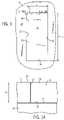
- FIG. 1illustrates a diagrammatic top plan view of a portion of a substrate at a preliminary processing stage according to an embodiment of the present disclosure, showing the substrate with a trench.
- FIGS. 1A-1Bare elevational, cross-sectional views of embodiments of the substrate depicted in FIG. 1 taken along lines 1 A/ 1 B- 1 A/ 1 B.
- FIGS. 2-5illustrate diagrammatic top plan views of the substrate of FIG. 1 at various stages of the fabrication of a self-assembled block copolymer film according to an embodiment of the present disclosure.
- FIGS. 2A-5Aillustrate elevational, cross-sectional views of embodiments of a portion of the substrate depicted in FIGS. 2-5 taken, respectively, along lines 2 A/ 2 A to lines 5 A- 5 A.
- FIGS. 6-7illustrate elevational, cross-sectional views of the substrate depicted in FIG. 5A , in subsequent stages.
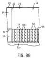
- FIG. 8illustrates a diagrammatic top plan view of a portion of the substrate of FIG. 7 at a subsequent stage.
- FIG. 8Ais an elevational, cross-sectional view of the substrate depicted in FIG. 8 taken along lines 8 A- 8 A.
- FIG. 8Bis a view of FIG. 8A in a subsequent processing step.
- FIG. 9illustrates a diagrammatic top plan view of a portion of a substrate at a preliminary processing stage according to another embodiment of the present disclosure, showing the substrate with a trench.
- FIG. 9Ais an elevational, cross-sectional view of the substrate depicted in FIG. 9 taken along lines 9 A- 9 A.
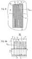
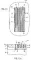
- FIGS. 10-13illustrate diagrammatic top plan views of the substrate of FIG. 9 at various stages of the fabrication of a self-assembled block copolymer film according to an embodiment of the present disclosure utilizing a cylindrical-phase block copolymer for the base film.
- FIGS. 10A-13Aillustrate elevational, cross-sectional views of embodiments of a portion of the substrate depicted in FIGS. 10-13 taken, respectively, along lines 10 A- 10 A to lines 13 A- 13 A.
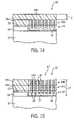
- FIGS. 14-17illustrate elevational, cross-sectional views of the substrate depicted in FIG. 13A , in subsequent stages.
- FIG. 17illustrates an intermediate structure showing the removal of half-cylindrical domains of the base layer.
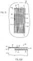
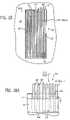
- FIG. 18illustrates a diagrammatic top plan view of a portion of the substrate of FIG. 17 at a subsequent stage.
- FIG. 18Aillustrates an elevational, cross-sectional view of the substrate depicted in FIG. 18 taken along lines 18 A- 18 A.
- FIG. 18Bis a view of FIG. 18A in a subsequent processing step.
- FIGS. 19-21illustrate diagrammatic top plan views of the substrate of FIG. 1 at various stages of the fabrication of a self-assembled block copolymer film according to another embodiment of the present disclosure utilizing a cylindrical-phase block copolymer for the base film.
- FIGS. 19A-21Aillustrate elevational, cross-sectional views of embodiments of a portion of the substrate depicted in FIGS. 19-21 taken, respectively, along lines 19 A- 19 A to lines 21 A- 21 A.
- FIGS. 22-23illustrate elevational, cross-sectional views of the substrate depicted in FIG. 21A , in subsequent stages.
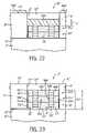
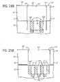
- FIG. 24illustrates a diagrammatic top plan view of a portion of the substrate of FIG. 23 showing the removal of cylindrical domains at a subsequent stage according to an embodiment of the invention.
- FIG. 24Aillustrates an elevational, cross-sectional view of the substrate depicted in FIG. 24 taken along lines 24 A- 24 A.
- FIG. 24Bis a view of FIG. 24A in a subsequent processing step.
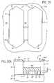
- FIG. 25illustrates a diagrammatic top plan view of a portion of the substrate of FIG. 24 showing the removal of the matrix domain at a subsequent stage according to another embodiment of the invention.
- FIG. 25Aillustrates an elevational, cross-sectional view of the substrate depicted in FIG. 25 taken along lines 25 A- 25 A.
- FIG. 25Bis a view of FIG. 25A in a subsequent processing step.
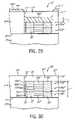
- FIG. 26illustrates a diagrammatic top plan view of the substrate of FIG. 1 at a subsequent stage of the fabrication of a self-assembled block copolymer film according to another embodiment of the present disclosure utilizing a cylindrical-phase block copolymer for the base film.
- FIG. 26Aillustrates an elevational, cross-sectional view of the substrate depicted in FIG. 26 taken along lines 26 A- 26 A.
- FIGS. 27-30illustrate elevational, cross-sectional views of the substrate depicted in FIG. 26A , in subsequent stages.
- FIG. 31illustrates a diagrammatic top plan view of a portion of the substrate of FIG. 30 showing the removal of cylindrical domains at a subsequent stage according to an embodiment of the invention
- FIG. 31Aillustrates an elevational, cross-sectional view of the substrate depicted in FIG. 31 taken along lines 31 A- 31 A.
- FIG. 31Bis a view of FIG. 31A in a subsequent processing step.
- FIG. 32illustrates a diagrammatic top plan view of a portion of the substrate of FIG. 30 showing the removal of the matrix domain at a subsequent stage according to another embodiment of the invention.
- FIG. 32Aillustrates an elevational, cross-sectional view of the substrate depicted in FIG. 32 taken along lines 32 A- 32 A.
- FIG. 32Bis a view of FIG. 32A in a subsequent processing step.
- semiconductor substrateor “semiconductive substrate” or “semiconductive wafer fragment” or “wafer fragment” or “wafer” will be understood to mean any construction comprising semiconductor material, including but not limited to bulk semiconductive materials such as a semiconductor wafer (either alone or in assemblies comprising other materials thereon), and semiconductive material layers (either alone or in assemblies comprising other materials).
- substraterefers to any supporting structure including, but not limited to, the semiconductive substrates, wafer fragments or wafers described above.
- L ois the inherent pitch (bulk period or repeat unit) of structures that self assemble upon annealing from a self-assembling (SA) block copolymer or a blend of a block copolymer with one or more of its constituent homopolymers.
- SAself-assembling
- Processing conditions of embodiments of the inventionuse a graphoepitaxy technique utilizing the sidewalls of trenches as constraints to induce orientation and registration of a first film of a self assembling diblock copolymer to form an ordered array pattern registered to the trench sidewalls.
- the first polymer filmis then used as a template or base layer for inducing the ordering of a subsequently deposited block copolymer film such that, upon annealing, the polymer domains orient and are registered to the underlying structures, resulting in a stacked double- or multi-layered structure with like polymer domains registered to each other,
- the procedurecan be repeated as needed to achieve a desired structure pattern of a required dimension in the z-axis direction.
- the desired patternedcan be selectively etched by methods known in the art, and the resulting template structures can be used to prepare features within a substrate.
- FIGS. 1-8Steps in a method for fabricating thin films from self assembling (SA) block copolymers that define nanometer-scale linear array patterns according to embodiments of the invention are illustrated in FIGS. 1-8 .
- SAself assembling
- the methodforms a multi-layer pattern within trenches by forming a polymer base film or template with ordered structures within the trenches for inducing the ordering of an overlying lamellar phase block copolymer film such that the lamellar domains are oriented perpendicularly and registered to the underlying assembled domains of the base film.
- the base layer within the trenchescan be formed from a lamellar-phase block copolymer film, which upon annealing forms a registered lamellar array of alternating polymer-rich blocks that extend the length and are oriented parallel to the sidewalls and perpendicular to the floor of the trenches.
- the base layeris formed from a cylindrical-phase block copolymer material which, upon annealing, forms lines of half-cylinders in a polymer matrix extending the length and oriented parallel to the sidewalls and floor of the trenches.
- the assembled base filmcan then be used as a template for inducing the ordering of an overlying lamellar-phase block copolymer film such that the lamellar domains of the annealed film are oriented perpendicularly and registered to the underlying pattern of the base film within the trenches.
- the surface of the sidewalls and edges of the trenchesare preferential wetting by one block of the copolymer and the trench floors are neutral wetting (equal affinity for both blocks of the copolymer) to allow both blocks of the copolymer material to wet the floor of the trench.
- Entropic forcesdrive the wetting of a neutral wetting surface by both blocks, resulting in the formation of a layer of perpendicular lamellae across the width of each trench.
- a substrate 10is provided bearing a neutral wetting surface.
- the substrate 10can comprise, for example, silicon (with native oxide), oxide (e.g., silicon oxide, SiO x ) or an inorganic film.
- a neutral wetting layer 12is formed on the substrate 10 prior to forming the overlying material layer 14 (e.g., oxide).
- Etching through the material layer 14 to form the trench 16exposes the underlying neutral wetting layer 12 as the floor or bottom surface 18 of the trench. Adjacent trenches are separated by a spacer or crest 20 .
- the trench 16is structured with opposing sidewalls 22 , opposing ends 24 , a width (w t ), a length (l t ) and a depth (D t ).
- a neutral wetting surfacecan be provided, for example, by applying a neutral wetting polymer to form a layer 12 on the surface of the substrate 10 .
- a neutral wetting polymerfor example, by applying a neutral wetting polymer to form a layer 12 on the surface of the substrate 10 .
- SAself-assembling
- PS-r-PMMArandom PS:PMMA copolymer brush layer
- the brushcan be affixed by grafting (on an oxide substrate) or by cross-linking (any surface) using UV radiation or thermal processing.
- a random copolymer solution composed of PS and PMMA with hydroxyl group(s)can be applied to the surface of the substrate 10 as a layer about 5-10 nm thick and grafted by heating at about 160° C. for about 48 hours.
- a surface that is neutral wetting to PS-b-PMMAcan be prepared by spin coating a blanket layer of a photo- or thermally cross-linkable random copolymer such as a benzocyclobutene- or azidomethylstyrene-functionalized random copolymer of styrene and methyl methacrylate (e.g., poly(styrene-r-benzocyclobutene-r-methyl methacrylate (PS-r-PMMA-r-BCB) onto the surface of the substrate 10 prior to forming the material layer 14 .
- a photo- or thermally cross-linkable random copolymersuch as a benzocyclobutene- or azidomethylstyrene-functionalized random copolymer of styrene and methyl methacrylate (e.g., poly(styrene-r-benzocyclobutene-r-methyl methacrylate (PS-r-PMMA-r-BCB) onto
- such a random copolymercan comprise about 42% PMMA, about (58-x) % PS and x % (e.g., about 2-3%) of either polybenzocyclobutene or poly(para-azidomethylstyrene)).
- An azidomethylstyrene-functionalized random copolymercan be UV crosslinked (e.g., 1-5 MW/cm ⁇ 2 exposure for about 15 seconds to about 30 minutes) or thermally crosslinked (e.g., at about 170° C. for about 4 hours).
- a benzocyclobutene-functionalized random copolymercan be thermally cross-linked (e.g., at about 200° C. for about 4 hours or at about 250° C. for about 10 minutes).
- Another neutral wetting surface for PS-b-PMMAcan be provided by hydrogen-terminated silicon, which can be prepared by a conventional process, for example, by a fluoride ion etch of a silicon substrate 10 (with native oxide present, about 12-15 ⁇ ) for example, by immersion in aqueous solution of hydrogen fluoride (HF) and buffered HF or ammonium fluoride (NH 4 F), by HF vapor treatment, by exposure to hot H 2 vapor, or by a hydrogen plasma treatment (e.g., atomic hydrogen).
- HFhydrogen fluoride
- NH 4 Fbuffered HF or ammonium fluoride
- the material layer 14can be formed on the substrate 10 and etched to form the trench 16 , and a neutral wetting material 12 then applied to the trench floor 18 .
- trench floors that are neutral wetting to PS-b-PMMAcan be prepared by spin coating PS-r-PMMA-r-BCB onto the surface of the substrate 10 within the trenches and thermally crosslinking the polymer (e.g., 190 ° C., 4 hours) to form a crosslinked polymer mat as a neutral wetting layer 12 . Capillary forces pull the random copolymer to the bottom of deep trenches. Non-crosslinked polymer material can be subsequently removed.
- a neutral-wetting polymersuch as random copolymer of P(S-r-MMA-r-HEMA) can also be grafted selectively to a material layer, e.g., an oxide floor.
- a material layere.g., an oxide floor.
- an olefinic monomersuch as PMMA or PS can be grafted onto an H-terminated silicon substrate 10 (i.e., floor 18 ) by an in situ free radical polymerization using a di-olefinic linker such divinyl benzene to produce an about 10-15 nm thick film.
- the trench sidewalls 22 and ends 24are preferential wetting by one block of the copolymer to induce formation of lamellae as the blocks self-assemble.
- the material layer 14 defining the trench surfacescan be an inherently preferential wetting material, or in other embodiments, a layer of a preferential wetting material can be applied onto the surfaces of the trenches.
- an oxidee.g., silicon oxide, SiO x
- a clean silicon surfacewith native silicon oxide
- a thin (e.g., 1 ⁇ 4 pitch) interface layer of PMMA and alternating PMMA and PS lamellaee.g,., 1 ⁇ 2 pitch
- PMMApolymethylmethacrylate
- a PMMA that is modified with a moiety containing one or more hydroxyl (—OH) groupscan be applied by spin coating and then heated (e.g., to about 170° C.) to allow the OH groups to end-graft to the oxide sidewalls 22 and ends 24 of the trenches.
- Non-grafted materialcan be removed from the neutral wetting layer 12 by rinsing with an appropriate solvent (e.g., toluene).
- an appropriate solvente.g., toluene
- toluenee.g., toluene
- the trench sidewalls, edges and floorsinfluence the structuring of the array of nanostructures within the trenches.
- the boundary conditions of the trench sidewalls in both the x- and y-axisimpose a structure wherein each trench contains n number of features (i.e., lamellae, cylinders, etc.).
- Factors in forming a single array or layer of nanostructures within the trenchesinclude the width and depth of the trench, the formulation of the block copolymer to achieve the desired pitch (L o ), and the thickness (t) of the copolymer film.
- the trenches 16are constructed with a width (w t ) such that a block copolymer (or blend) will self assemble upon annealing into a single layer of “n” structures spanning the width (w t ) of the trench, with each structure (i.e., lamellae, cylinders, etc.) being separated by a value of L o (from center-to-center).
- the width (w t ) of the trenchesis a multiple of the inherent pitch value (L o ) of the polymer being equal to or about nL o (“n*L o ”), typically ranging from about n*10 to about n*100 nm (with n being the number of features or structures).
- the depth (D t ) of the trenchesis a multiple of the L o value of the block copolymer used for the base layer.
- the application and annealing of a block copolymer material having an inherent pitch value of L o in a trench having a width (w t ) at or about L owill result in the formation of a single layer of “n” structures spanning the width and registered to the sidewalls for the length of the trench.
- the trench dimensionis about 50-500 nm wide (w t ) and about 1,000-10,000 ⁇ m in length (l t ), with a depth (D t ) of about 20-200 nm.
- the trenchescan be formed using a lithographic tool having an exposure system capable of patterning at the scale of L o (10-100 nm).
- exposure systemsinclude, for example, extreme ultraviolet (EUV) lithography, proximity X-rays, and electron beam (e-beam) lithography, as known and used in the art.
- EUVextreme ultraviolet
- e-beamelectron beam
- Conventional photolithographycan attain (at smallest) about 58 nm features.
- a layer 26 of a self-assembling (SA) lamellar-phase diblock copolymer material having an inherent pitch at or about L o (or a ternary blend of block copolymer and homopolymers blended to have a pitch at or about L o )is then deposited, typically by spin casting (spin-coating) onto the floor 18 of the trench.
- the block copolymer materialcan be deposited onto the patterned surface by spin casting from a dilute solution (e.g., about 0.25-2 wt % solution) of the copolymer in an organic solvent such as dichloroethane (CH 2 Cl 2 ) or toluene, for example.
- the thickness (t l ) of the diblock copolymer layer 26is less than the trench depth (D t ) and at or about the L o value of the copolymer material such that the film layer will self assemble upon annealing to form a single layer of lamellae across the width (w t ) of the trench.
- a typical thickness (t l ) of the copolymer film 26is about ⁇ 20% of the L o value of the copolymer (e.g., about 10-100 nm) to form alternating polymer-rich lamellar blocks having a width of about L o (e.g., 25-35 nm) in a matrix of another block within each trench.
- the thickness of the film 26can be measured, for example, by ellipsometry techniques. As shown, a thin film 26 of the copolymer material can be deposited onto the spacers 20 of the material layer 14 ; this film will not self-assemble, as it is not thick enough to form structures.
- diblock copolymersare used in the illustrative embodiments of this disclosure, other types of block copolymers (i.e., triblock or multiblock copolymers) can be used.
- diblock copolymersinclude poly(styrene-block-methyl methacrylate) (PS-b-PMMA), polyethyleneoxide-polyisoprene, polyethyleneoxide-polybutadiene, polyethyleleoxide-polystyrene, polyetheleneoxide-polymethylmethacrylate, polystyrene-polylpyridine, polystyrene-polyisoprene (PS-b-PI), polystyrene-polybutadiene, polybutadiene-polyvinylpyridine, and polyisoprene-polymethylmethacrylate, among others.
- PS-b-PMMApoly(styrene-block-methyl methacrylate)
- PS-b-PMMApolyethylene
- triblock copolymersexamples include poly(styrene-block methyl methacrylate-block-ethylene oxide).
- One of the polymer blocks of the block copolymershould be selectively and readily removable in order to fabricate an etch mask or template from the annealed film.
- the volume fractions of the two blocks (AB)are generally at a ratio between about 50:50 and 60:40.
- the Chi value of the polymer blocks (e.g., PS and PMMA) at common annealing temperaturesis generally small such that the air interface is equally or non-selectively wetting to both blocks.
- An example of a lamellae-forming symmetric diblock copolymeris PS-b-PMMA with a weight ratio of about 50:50 (PS:PMMA) and total molecular weight (M n ) of about 51 kg/mol.
- the block copolymer materialcan also be formulated as a binary or ternary blend comprising a SA block copolymer and one or more homopolymers of the same type of polymers as the polymer blocks in the block copolymer, to produce blends that swell the size of the polymer domains and increase the L o value of the polymer.
- the volume fraction of the homopolymerscan range from 0 to about 40%.
- An example of a ternary diblock copolymer blendis a PS-b-PMMA/PS/PMMA blend, for example, 46K/21K PS-b-PMMA containing 40% 20K polystyrene and 20K poly(methylmethacrylate).
- the L o value of the polymercan also be modified by adjusting the molecular weight of the block copolymer, e.g., for lamellae, L o ⁇ (MW) 2/3 .
- ellipticitycan be induced in the structures by creating a slight mismatch between the trench and the spacer widths and the inherent pitch (L o ) of the block copolymer or ternary blend, as described, for example, by Cheng et al., “Self-assembled One-Dimensional Nanostructure Arrays,” Nano Lett., 2006, 6(9), 2099-2103, the disclosure of which are incorporated by reference herein, which then reduces the stresses that result from such mismatches.
- the first block copolymer film 26is then annealed, for example, by thermal annealing to above the glass transition temperature of the component blocks of the copolymer material to cause the polymer blocks to phase separate and self assemble according to the preferential and neutral wetting of the trench surfaces 18 , 22 , 24 to form a self-assembled polymer structure 28 .
- a PS-b-PMMA copolymer filmcan be annealed at a temperature of about 180-285° C. in a vacuum oven for about 1-120 hours to achieve the self-assembled morphology.
- the filmcan also be solvent annealed, for example, by slowly swelling both blocks of the film with a solvent, then slowly evaporating the solvent.
- the constraints provided by the width (w t ) of the trenches and the character of the copolymer composition combined with preferential or neutral wetting surfaces within the trenchesresults, upon annealing, in a single layer of n elements (lamellae) across the width (w t ) of the trench.
- the number “n” or pitches of elements (e.g., lamellar blocks) or half-cylinders within a trenchis according to the width (w t ) of the trench and the molecular weight (MW) of the block copolymer. As shown in FIG.
- a lamellar-phase block copolymer material used to form the base layer 28will, upon annealing, self assemble into perpendicular-oriented, alternating polymer-rich blocks 30 , 32 spanning the width (w t ) of the trench 16 at an average pitch value at or about L o .
- the resulting morphologies of the annealed base film 28can be examined, for example, using atomic force microscopy (AFM), transmission electron microscopy (TEM), scanning electron microscopy (SEM).
- AFMatomic force microscopy
- TEMtransmission electron microscopy
- SEMscanning electron microscopy
- the annealed and ordered base film 28is then treated to crosslink the polymer segments to fix and enhance the strength of the self-assembled polymer blocks 30 , 32 within the trench 16 (e.g., to crosslink the PS segments).
- the polymerscan be structured to inherently crosslink (e.g., upon exposure to ultraviolet (UV) radiation, including deep ultraviolet (DUV) radiation), or one or both of the polymer blocks of the copolymer material can be formulated to contain a crosslinking agent.
- UV radiationultraviolet
- DUV radiationdeep ultraviolet
- the trench regionscan be selectively exposed through a reticle to crosslink only the self-assembled film 28 within the trench 16 , and a wash can then be applied with an appropriate solvent (e.g., toluene), to remove the non-crosslinked portions of the film 28 (e.g., material 26 on the spacer 20 ) leaving the registered self-assembled base film within the trench and exposing the surface of material layer 14 above/outside the trench (e.g., the spacer 20 ).
- an appropriate solvente.g., toluene
- the annealed film 28can be crosslinked globally, a photoresist layer can be applied to pattern and expose the areas of the film outside the trench regions (e.g., over the spacers 20 ), and the exposed portions of the film can be removed, for example by an oxygen (O 2 ) plasma treatment.
- the spacers 20are narrow in width, for example, a width (w s ) of one of the copolymer domains (e.g., about L o ) such that the material 26 on the spacers is minimal and no removal is required.
- a layer 34 a of a lamellar-phase block copolymer material having an inherent pitch at or about L ois then deposited (e.g., by spin casting) onto the annealed and crosslinked base film 28 within the trench.
- the block copolymer materialcan be spin cast, for example, from a dilute solution of the copolymer in an organic solvent (e.g., about 0.25-2 wt % solution).
- the lamellar-phase block copolymer layer 34 ais cast onto the base film 28 within the trench 16 to a thickness (t 2 ) at or about the L o value of the block copolymer material such that, upon annealing, the copolymer film layer will self-assemble to form a single layer of perpendicular-oriented lamellar domains, each having a width (w 2 ) at or about 0.5 L o .
- annealing of the lamellar-phase block copolymer layer 34 ais then conducted to cause the polymer blocks to separate and self assemble into a film 36 a composed of perpendicular-oriented lamellar-phase domains 38 a , 40 a in a striped pattern, which are ordered and registered, respectively, to the polymer domains 30 , 32 of the base layer 28 .
- Annealingcan be conducted, for example, over a range of about 110-290° C. for a PS-b-PMMA copolymer film.
- the annealed film 36 ais then crosslinked, and the non-ordered copolymer material 34 a on the material layer 14 outside the trench 16 can be removed (e.g., by solvent wash, O 2 plasma treatment) resulting in the structure shown in FIG. 5A .
- a second layer 34 b of the lamellar-phase block copolymer materialcan be deposited to a thickness (t 2 ) at or about L o onto the annealed and crosslinked film 36 a .
- the block copolymer layer 34 bcan then be annealed such that the polymer blocks self assemble into a film 36 b of perpendicular-oriented lamellar-phase domains 38 b , 40 b oriented and registered to the underlying polymer blocks 38 a , 40 a , whereupon the film 36 b can be crosslinked and non-ordered copolymer material 34 b outside the trench 16 can be removed, as illustrated in FIG. 7 .
- the aspect ratio of the openings formed in the multilayered filmis at least about two times the aspect ratio that can be provided by similar single layer films, and can be increased with the addition of film layers, generally at least about 1:2 and ranging from about 1:2 to about 1:20.
- one of the block componentscan be selectively removed to produce a thin film 44 that can be used, for example, as a lithographic template or mask to pattern the underlying substrate 10 in a semiconductor processing to define regular patterns in the nanometer size range (i.e., about 10-100 nm).
- a lithographic template or maskto pattern the underlying substrate 10 in a semiconductor processing to define regular patterns in the nanometer size range (i.e., about 10-100 nm).
- Removal of PMMA phase domainscan be performed, for example, by application of an oxygen (O 2 ) or CF 4 plasma.
- the openingsare separated by walls composed of the PMMA domains.
- the resulting film 44has a corrugated surface that defines a linear pattern of fine, nanometer-scale, parallel slits (openings) 46 about 5-50 nm wide and several microns in length (e.g., about 10-4000 ⁇ m), the individual slits separated by walls 48 about 5-50 nm wide, providing an aspect ratio ranging from about 1:2 to about 1:20.
- openingsfine, nanometer-scale, parallel slits
- the individual slits separated by walls 48about 5-50 nm wide, providing an aspect ratio ranging from about 1:2 to about 1:20.
- removal of the PMMA domainsaffords a PS mask of sublithographic dimensions, for example, a pitch of about 35 nm (17.5 nm PS domain). A smaller pitch can be dialed in by using lower molecular weight diblock copolymers.
- the filmscan be used, for example, as a lithographic template or etch mask to pattern (arrows ⁇ ) the underlying substrate 10 , for example, by a non-selective RIE etching process, to delineate a series of channels or grooves 50 , shown in phantom in FIG. 8A , and extending to an active area or element 51 a .
- the channels 50can then be filled with a material 51 b as illustrated in FIG. 8B , for example, a conductive material (e.g., metal) to form nanowire channel arrays for transistor channels, semiconductor capacitors, and other structures, or with a dielectric material to separate active areas (e.g., substrate 10 ). Further processing can then be performed as desired.
- the filmsprovide linear arrays having long range ordering and registration for a wide field of coverage for templating a substrate.
- the filmsare useful as etch masks for producing close pitched nanoscale channel and grooves that are several microns in length, for producing features such as floating gates for NAND flash with nanoscale dimensions.
- photolithography techniquesare unable to produce channels much below 60 nm wide without high expense. Resolution can exceed other techniques such as conventional photolithography, while fabrication costs utilizing methods of the disclosure are far less than electron beam (E-beam) or EUV photolithographies which have comparable resolution.
- a method according to another embodiment of the invention for forming a thin film that defines a linear array pattern utilizing a base layer formed from a cylindrical-phase block copolymeris illustrated with reference to FIGS. 9-18 .
- the base layerupon annealing, forms lines of half-cylinders in a polymer matrix extending the length and oriented parallel to the sidewalls and floor of the trenches.
- the assembled base filmcan then be used as a template for inducing the ordering of an overlying lamellar-phase block copolymer film such that the lamellar domains of the annealed film are oriented perpendicularly and registered to the underlying pattern of the half-cylinders of the base film.
- the surfaces of the floor 18 ′, sidewalls 22 ′ and ends 24 ′ of the trenchare preferential wetting by the minority block of the copolymer to induce formation of parallel lines of half-cylinders of the minority block wetting the air interface (surface exposed) down the middle of each trench aligned parallel to the trench sidewalls and floor.
- substrate 10 ′can be composed of an inherently preferential wetting material such as a clean silicon surface (with native silicon oxide) and material layer 14 ′ can be composed of oxide (e.g., SiO x ).
- Both materialsexhibit preferential wetting toward the PMMA block to result in the assembly of a thin interface layer of PMMA on the trench sidewalls as well as PMMA cylinders in the center of a PS matrix within each trench.
- Other preferential wetting surfaces to PMMAcan be provided, for example, by silicon nitride, silicon oxycarbide, and PMMA polymer grafted to a sidewall material such as silicon oxide, and resist materials such as such as methacrylate-based resists. See, for example, C. T. Black and O. Bezencenet, “Nanometer-Scale Pattern Registration and Alignment by Directed Diblock Copolymer Self-Assembly,” IEEE Transactions on Nanotechnology, 2004, 3(3), 412-415; C. T.
- the depth (D t ) of the trench 16 ′is less than L o
- the trench dimensionis about 50-2000 nm wide (w t ) with a depth (D t ) of about 15-25 nm. As shown in FIG.
- a layer 26 ′ of the cylinder-forming block copolymer material(inherent pitch at or about L o ) is deposited onto the floor 18 ′ of the trench 16 ′ to a thickness (t l ) greater than the trench depth (D t ) but less than about the L o value of the block copolymer material such that the copolymer film 26 ′ will self assemble upon annealing to form a single layer of parallel-oriented half-cylinders of one block having a diameter of about L o in a matrix of another block as parallel lines across the width (w t ) of the trench.
- the number “n” or pitches of half-cylinders within a trenchis according to the width (w t ) of the trench (e.g., about nL o ) and the molecular weight (MW) of the block copolymer.
- the cylindrical-phase block copolymercan be a diblock or multiblock copolymer, and the copolymer material can be formulated as a binary or ternary blend comprising a homopolymer(s), as previously described.
- the volume fractions of the two blocks (AB)are generally at a ratio between about 60:40 and 80:20.
- M ntotal molecular weight
- the Chi value of the polymer blocks (e.g., PS and PMMA) at common annealing temperatures and the difference between interfacial energies of each block and the airis generally small, such that the air interface is equally or non-selectively wetting to both blocks.
- the cylindrical-phase block copolymer film 26 ′is annealed to form the base layer 28 ′, resulting in parallel-oriented half-cylinders 30 ′ within a polymer matrix 32 ′ spanning the width (w t ) of the trench 16 ′, with each cylinder being separated by an average value of at or about LF, and an interface layer 30 a ′ along the sidewalls 22 ′ and floor 18 ′.
- a thin film 26 ′ of the copolymer material deposited on the spacers or crests 20 ′ of the material 14 ′ between trenchesis not thick enough to self-assemble.
- the spacers 20 ′ between the trenchesare narrow, for example, having a width (w s ) of one of the copolymer domains such that the material 26 ′ on the spacers 20 ′ is essentially nonexistent.
- the annealed base film 28 ′is then be treated to crosslink the polymer segments (e.g., to crosslink the PS matrix 32 ′).
- the polymerscan be structured to inherently crosslink, or one or both of the polymer blocks of the copolymer material can be formulated to contain a crosslinking agent.
- a layer 34 a ′ of a lamellar-phase block copolymer material(inherent pitch at or about L o ) is then deposited onto the annealed and crosslinked base film 28 ′ to a thickness (t 2 ) at or about the L o value of the lamellar-phase block copolymer material.
- the lamellar-phase block copolymer materialcan be structured and formulated as previously described with respect to the embodiment of FIGS. 1-8 .
- the volume fractions of the two blocks (AB) of a lamellar-forming diblock copolymerare generally at a ratio between about 50:50 and 60:40, an example being a PS-b-PMMA copolymer at a 50:50 weight ratio (M n of about 51 kg/mol), with a generally small difference in interfacial energies of each block with air to produce surface-exposed lamellae.
- a self-assembled film 36 a ′composed of a single layer of perpendicular-oriented lamellar-phase domains 38 a ′, 40 a ′ in a striped pattern, which are ordered and registered, respectively, to the polymer domains 30 ′, 32 ′ of the cylindrical-phase base layer 28 ′, as illustrated in FIG. 13-13A ) with each domain having a width (w 2 ) of about L o .
- the copolymer material 34 a ′ on the spacers 20 ′may self-assemble but without registration or long-range order.
- the annealed film 36 a ′is then treated to crosslink the polymer segments (e.g., PS domains 40 a ′), as previously described.
- a second layer 34 b ′ of a lamellar-phase block copolymer materialcan then be deposited onto the previously annealed and crosslinked film 36 a ′ to a thickness (t 2 ) at or about L o .
- the second copolymer layer 34 b ′can then be annealed to form a second film layer 36 b ′ composed of lamellar-phase domains 38 b ′, 40 b ′ oriented and registered to the underlying polymer blocks 38 a ′, 40 a ′, resulting in the structure shown in FIG. 15 .
- the copolymer material 34 b ′ over the copolymer layer 34 a ′ on the spacers 20 ′may self-assemble but without registration or long-range order.
- the film 36 b ′can then be crosslinked, and additional layers of the lamellar-phase block copolymer can be deposited, annealed and crosslinked to form a film structure 42 ′ of the desired thickness (T).
- the additional layers of the self-assembled and crosslinked filmcan be added to increase the aspect ratio of the openings subsequently formed in the multilayered film.
- the non-ordered copolymer material 34 a ′, 34 b ′ remaining on the spacers 20 ′can then be removed resulting in the structure shown in FIG. 16 .
- a solvent washcan be applied to remove residual copolymer material from the spacers 20 ′ that has not been cross-linked (e.g., it was masked during crosslinking of the polymer layers).
- Photo-patterning and a selective O 2 plasma etchcan be used to remove crosslinked polymer material from the spacers 20 ′.
- Selective removal of one of the polymer blocks of the layers 36 a - b ′ and the base film 28 ′can then be performed to produce a thin film 44 ′ with openings/slits that expose the underlying substrate 10 ′ and can be used as an etch mask.
- the matrix 32 ′e.g., PS
- That portion of matrix 32 ′can be removed, for example, by a plasma O 2 or CF 4 etch, prior to a patterning process to expose the underlying substrate 10 ′, resulting in the film 44 ′ illustrated in FIGS. 18-18A .
- the filmcan be used, for example, to pattern (arrows ⁇ ) the underlying substrate 10 ′ to delineate a series of channels or grooves 50 ′, shown in phantom in FIG. 18A , to an active area or element 51 a ′, which can then be filled with a material 51 b ′, for example, a conductive metal or dielectric material, as depicted in FIG. 18B .
- a method according to another embodiment of the invention for forming thin films of a cylindrical-phase self assembling block copolymer that define an array of perpendicularly-oriented cylinders in a polymer matrixis illustrated with reference to FIGS. 19-25 .
- the described embodimentutilizes topographical features, the sidewalls and ends of trenches, as constraints to induce orientation and registration of cylindrical copolymer domains to achieve a hexagonal array of perpendicularly-oriented cylinders within a polymer matrix registered to the trench sidewalls.
- a trench 16 ′′is etched in a material layer 14 ′′ to expose a neutral wetting surface on an underlying substrate 10 ′′.
- the width (w t ) of the trench 16 ′′is at or about nL o .
- the ends 24 ′′are angled to the sidewalls as shown, for example, at an about 60° angle, and in some embodiments are slightly rounded.
- the trenchesare also structured such that the trench floor 18 ′′ is neutral wetting to both blocks of the copolymer material, and the sidewalls 22 ′′ and ends 24 ′′ are preferential wetting by the minority block of the copolymer. Entropic forces drive the wetting of a neutral-wetting surface by both blocks, resulting in a perpendicular orientation of the self-assembled cylinders.
- the material layer 14 ′′is composed of silicon oxide (SiO x ) and the substrate 10 ′′ is composed of silicon.
- a neutral wetting layer 12 ′′can be provided, for example, by applying a neutral wetting polymer on the surface of the substrate 10 ′′ before forming the material layer 14 ′′, and the trenches 16 ′′ can be etched expose the neutral wetting layer 12 ′′ forming the trench floors 18 ′′.
- a neutral wetting polymere.g., PS-r-PMMA, PS-r-PMMA-r-BCB, etc.
- a neutral wetting surface for PS-b-PMMAcan be provided by hydrogen-terminated silicon, or by PS-r-PMMA ( ⁇ 60 mol % PS) graft polymerized in situ onto H-terminated silicon.
- sidewalls 22 ′′ and ends 24 ′′ that are preferential wetting toward the PMMA block of a PS-b-PMMA diblock copolymercan be provided by a material layer 14 ′′ composed of silicon oxide (SiO x ), silicon nitride, silicon oxycarbide, a PMMA polymer modified with a moiety containing hydroxyl (—OH) group(s) (e.g., hydroxyethylmethacrylate) grafted to a sidewall material such as silicon oxide, and resist materials such as such as methacrylate based resists.
- a material layer 14 ′′composed of silicon oxide (SiO x ), silicon nitride, silicon oxycarbide, a PMMA polymer modified with a moiety containing hydroxyl (—OH) group(s) (e.g., hydroxyethylmethacrylate) grafted to a sidewall material such as silicon oxide, and resist materials such as such as methacrylate based resists.
- a cylindrical-phase diblock copolymer material 26 ′′ having an inherent pitch at or about L o (or blend with homopolymers)is deposited onto the neutral wetting layer 12 ′′ on the floor 18 ′′ of the trench 16 ′′ to a thickness (t l ) of less than or about equal to the L o value of the copolymer material to up to about 1.5 ⁇ L o , such that the copolymer film layer will self assemble upon annealing to form a hexagonal array of perpendicular cylindrical domains having a diameter of about 0.5 L o (e.g., about 20 nm) in the middle of a polymer matrix within each trench (e.g., with the adjacent cylindrical domains having a center-to-center distance of at or about L o (e.g., about 35 nm).
- L oe.g., about 20 nm
- the volume fractions of the two blocks (AB)are generally at a ratio between about 60:40 and 80:20.
- the block copolymer film 269 ′′is then annealed, resulting in a base film 28 ′′.
- the character of the block copolymer composition 26 ′′ combined with a neutral wetting trench floor 18 ′′ and preferential wetting sidewalls 22 ′′ and ends 24 ′′, and constraints provided by the width (w t ) of trench 16 ′′results, upon annealing, in a hexagonal array of perpendicularly-oriented cylindrical domains 30 ′′ of the minor polymer block (i.e., like domains) (e.g., PMMA) within a matrix 32 ′′ of the major polymer block (e.g., PS).
- the minor polymer blocki.e., like domains
- the major polymer blocke.g., PS
- a thin layer 30 a ′′ of the minor polymer blockwets the sidewalls 18 ′′.
- the hexagonal arraycontains n single rows of cylinders according to the width (w t ) of the trench with the cylinders 30 ′′ in each row being offset by about L o (pitch distance or center-to-center distance) from the cylinders in the adjacent rows.
- Each rowcontains a number of cylinders, generally mn cylinders, which number can vary according to the length (l t ) of the trench and the shape of the trench end (e.g., rounded, angled, etc.) with some rows having greater or less than m cylinders.
- the pitch distance between each cylinder 30 ′′ (within a row)is generally at or about L o .
- the annealed cylindrical-phase base film 28 ′′is then treated to crosslink the polymer segments (e.g., to crosslink the PS matrix 32 ′′).
- the polymerscan be structured to inherently crosslink, or one or both of the polymer blocks of the copolymer material can be formulated to contain a crosslinking agent.
- the polymer material remaining on the spacers 20 ′′can then be removed as previously described.
- a layer 34 a ′′ of a cylindrical-phase block copolymer material(inherent pitch at or about L o ) is then deposited onto the annealed and crosslinked base film 28 ′′ to a thickness (t 2 ) at or about the L o value of the cylindrical-phase block copolymer material 36 a ′′.
- annealing of the block copolymer layer 34 a ′′results in a film 36 a ′′ composed of a single layer of a hexagonal array of perpendicular-oriented cylindrical domains 38 a ′′ within a polymer matrix 40 a ′′ which are ordered and registered to the underlying cylindrical domains 30 ′′ and matrix 32 ′′ of the base layer 28 ′′, as illustrated in FIG.
- the annealed film 36 a ′′is then treated to crosslink the polymer segments (e.g., PS matrix 40 a ′′) and the polymer material on the spacers 20 ′′ removed, as previously described.
- a second layer 34 b ′′ of the cylindrical-phase block copolymer materialcan be deposited onto the annealed and crosslinked film 36 a ′′ to a thickness (t 2 ) at or about L o ( FIG. 22 ), and annealed to form a second film layer 36 b ′′ composed of perpendicular-oriented cylindrical domains 38 b ′′ in a matrix 40 b ′′, which are oriented and registered to the underlying cylinders 38 a ′′ and matrix 40 a ′′, as depicted in FIG. 23 .
- the film 36 b ′′is then crosslinked, and the polymer material on the spacers 20 ′′ can be removed to produce the film structure 42 ′′ as shown. Additional layers of the cylindrical-phase diblock copolymer can be deposited, annealed and crosslinked to form a film structure of a desired thickness (T) and to increase the aspect ratio of the openings formed in the multilayered film.
- Tdesired thickness
- One of the block componentscan then be selectively removed from the film 42 ′′, leaving either the matrix 48 ′′ to produce a film 44 a ′′ composed of a hexagonal array of cylindrical openings 46 ′′ as in FIGS. 24-24A , or the cylindrical domains 52 ′′ to produce a film 44 b ′′ as in FIGS. 25-25A .
- the resulting films 44 a ′′, 44 b ′′can be used, for example, as a lithographic template or mask to pattern the underlying substrate 10 ′′ in a semiconductor processing to define regular patterns in the nanometer size range (i e., about 5-50 nm).
- a film 44 a ′′composed of a hexagonal array of openings 46 ′′ within the matrix 48 ′′ of the major block (e.g., PS), the openings having a diameter of about 5-50 nm and an aspect ratio generally at least about 1:2 and ranging from about 1:2 to about 1:20.
- the film 44 a ′′can be used as an etch mask to pattern (arrows ⁇ ) the underlying substrate 10 ′′ to form an array of openings 50 ′′ in the substrate 10 ′′ (shown in phantom in FIG.
- a metal or conductive alloysuch as Cu, Al, W, Si, and Ti 3 N 4 , among others, to form contacts, for example, to an underlying active area or conductive line 51 a ′′, or with a metal-insulator-metal-stack to form capacitors with an insulating material such as SiO 2 , Al 2 O 3 , HfO 2 , ZrO 2 , SrTiO 3 , among other dielectrics.
- the selective removal of the major block matrix 32 ′′/ 40 a - b ′′will provide a film 44 b ′′ composed of a hexagonal array of the minor block cylinders 52 ′′ (e.g., PS).
- a majority PMMA block copolymer and sidewallscomposed of a material that is selectively PS-wetting (e.g., a gold sidewall or PS-grafted to the sidewall material).
- the film 44 b ′′ composed of cylinders 52 ′′can be used as an etch mask (arrows ⁇ ) to etch a patterned opening 54 ′′ in the underlying substrate 10 ′′ (shown in phantom in FIG.
- openings 54 ′′ in a silicon substrate 10 ′′can be filled with a dielectric material such as SiO 2 , with the cylinders of the residual substrate 1 0 ′′ (e.g., of silicon) providing contacts to an underlying active area or metal lines 51 a′′.
- the foregoing process for forming a hexagonal array of cylinders with a cylindrical-phase block copolymercan be modified by utilizing the trench sidewalls and ends as constraints to induce orientation and registration of cylindrical copolymer domains in a single row parallel to the trench sidewalls.
- a trench 16 ′′is structured to have a width (w t ) that is at or about the L o value of the block copolymer material, a floor 18 ′′′ that is neutral wetting to both blocks of the copolymer material, and sidewalls 22 ′′′ and ends 24 ′′′ that are preferential wetting by the minority block of the copolymer.
- the material layer 14 ′′′(e.g., SiO x , SiN, etc.) exposed on the sidewalls 22 ′′′ and ends 24 ′′′ is preferential wetting toward the PMMA block of a PS-b-PMMA diblock copolymer, and the substrate 10 ′′′ (e.g., silicon) bears a neutral wetting layer 12 ′′′ (e.g., a neutral wetting polymer, H-terminated silicon) which is exposed at the trench floors 18 ′′′.
- a neutral wetting layer 12 ′′′e.g., a neutral wetting polymer, H-terminated silicon
- a cylindrical-phase diblock copolymer material 26 ′′′ having an inherent pitch at or about L o (or blend with homopolymers)can be deposited onto the neutral wetting layer 12 ′′′ on the trench floor 18 ′′′ to a thickness (t l ) of less than or about equal to the L o value of the copolymer material to up to about 1.5 ⁇ L o (as shown in FIGS. 2-2A ).
- the block copolymer film 26 ′′′is then annealed, whereupon the copolymer film layer will self assemble to form a base film 28 ′′′, as illustrated in FIGS. 26-26A .
- the cylindershave a diameter at or about 0.5 L o (e.g., about 20 nm), the number n of cylinders in the row is according to the length of the trench, and the center-to-center distance (pitch distance) (p) between each like domain (cylinder) is at or about L o (e.g., about 35 nm).
- the annealed cylindrical-phase base film 28 ′′′is then treated to crosslink the polymer segments (e.g., the PS matrix 32 ′′′).
- Processingcan then be continued to form a cylindrical-phase block copolymer layer 36 a ′′′ on the base film ( FIG. 27 ), which upon annealing results in a single layer of perpendicular cylindrical domains 38 a ′′′ within a polymer matrix 40 a ′′′, which are ordered and registered to the underlying cylindrical domains 30 ′′′ and matrix 32 ′′′ of the base layer 28 ′′′ ( FIG. 28 ).
- the film 36 a ′′′is then treated to crosslink the polymer segments (e.g., PS matrix 40 a ′′′) as previously described.
- a second layer 34 b ′′′ of the cylindrical-phase block copolymercan then be deposited onto the annealed/crosslinked film 36 a ′′′ to a thickness (t 2 ) at or about L o ( FIG. 29 ) and annealed.
- the resulting film 36 b ′′′( FIG. 30 ) is composed of perpendicular-oriented cylindrical domains 38 b ′′′ in a matrix 40 b ′′′ oriented and registered to the underlying cylinders 38 a ′′′ and matrix 40 a ′′′ of film 36 a ′′′.
- the film 36 b ′′′is crosslinked, and non-ordered polymer material on the spacers 20 ′′′ can be removed to produce the film structure 42 ′′′. Additional layers of the cylindrical-phase diblock copolymer can be deposited, annealed and crosslinked to form a film structure of a desired thickness (T).
- Selective removal of one of the block componentscan then be performed resulting in a film 44 a ′′′ composed of the matrix 48 ′′′ with a 1-D array of cylindrical openings 46 ′′′ as in FIGS. 31-31A .
- selective removal of the matrix components 32 ′′′/ 40 a - b ′′′produces a film 44 b ′′′ composed of a 1-D array of cylinders 52 ′′′ as in FIGS. 32-32A .
- the filmcan be used as a mask to etch the underlying substrate 10 ′′′.
- a film 44 a ′′′composed of a 1-D array of openings 46 ′′′ within the matrix 48 ′′′ of the major block (e.g., PS), the openings having a diameter of about 5-50 nm and an aspect ratio of about 1:2 to about 1:20.
- the film 44 a ′′′can be used as an etch mask to pattern (arrows ⁇ ) the underlying substrate 10 ′′′ to form an array of openings 50 ′′′ (shown in phantom in FIG.
- FIG. 31Aa material 51 b ′′′, for example, a metal or conductive alloy to provide a 1-D array of contacts to an underlying active area or line contact 51 a ′′′, for example, or with metal-insulator-metal-stacks to form capacitors. Further processing can then be performed as desired.
- a material 51 b ′′′for example, a metal or conductive alloy to provide a 1-D array of contacts to an underlying active area or line contact 51 a ′′′, for example, or with metal-insulator-metal-stacks to form capacitors. Further processing can then be performed as desired.
- the selective removal of the major block matrix components 32 ′′′, 40 a - b ′′′will provide a film 44 b ′′′ composed of a 1-D array of the minor block cylinders 52 ′′′ (e.g., PS).
- the film 44 b ′′′can be used as a mask or template in an etch process (arrows ⁇ ) to form a patterned opening 54 ′′′ (shown in phantom in FIG. 32A ) in the underlying substrate 10 ′′′, with the masked substrate 10 ′′′ etched to form cylinders.
- the residual cylinders 52 ′′′ of the polymer mask 44 b ′′′can then be removed and a material 51 b ′′′ such as a dielectric material (e.g., oxide) that is distinct from the substrate 10 ′′′ (e.g., silicon) can be deposited to fill the opening 54 ′′ as shown in FIG. 32B , to provide a differential surface to the substrate 10 ′′ cylinders, which can provide contacts to an underlying active area or metal line 51 a ′′′, for example.
- a material 51 b ′′′such as a dielectric material (e.g., oxide) that is distinct from the substrate 10 ′′′ (e.g., silicon) can be deposited to fill the opening 54 ′′ as shown in FIG. 32B , to provide a differential surface to the substrate 10 ′′ cylinders, which can provide contacts to an underlying active area or metal line 51 a ′′′, for example.
- a material 51 b ′′′such as a dielectric material (e.g., oxide
Landscapes
- Engineering & Computer Science (AREA)
- Chemical & Material Sciences (AREA)
- Physics & Mathematics (AREA)
- Manufacturing & Machinery (AREA)
- General Physics & Mathematics (AREA)
- Microelectronics & Electronic Packaging (AREA)
- Nanotechnology (AREA)
- Condensed Matter Physics & Semiconductors (AREA)
- Computer Hardware Design (AREA)
- Power Engineering (AREA)
- Crystallography & Structural Chemistry (AREA)
- Inorganic Chemistry (AREA)
- Mathematical Physics (AREA)
- Theoretical Computer Science (AREA)
- Analytical Chemistry (AREA)
- Graft Or Block Polymers (AREA)
- Exposure Of Semiconductors, Excluding Electron Or Ion Beam Exposure (AREA)
- Treatments Of Macromolecular Shaped Articles (AREA)
- Photosensitive Polymer And Photoresist Processing (AREA)
- Formation Of Insulating Films (AREA)
- Drying Of Semiconductors (AREA)
Abstract
Description
- Embodiments of the invention relate to methods of fabricating nanoscale arrays of micro-vias, microchannels and microstructures by use of thin films of self-assembling block copolymers, and devices resulting from those methods.
- As the development of nanoscale mechanical, electrical, chemical and biological devices and systems increases, new processes and materials are needed to fabricate nanoscale devices and components. Conventional optical lithographic processing methods are not able to accommodate fabrication of structures and features much below the 100 nm level. The use of self assembling diblock copolymers presents another route to patterning at nanometer dimensions. Diblock copolymer films spontaneously assembly into periodic structures by microphase separation of the constituent polymer blocks after annealing, for example by thermal annealing above the glass transition temperature of the polymer or by solvent annealing, forming ordered domains at nanometer-scale dimensions. Following self assembly, one block of the copolymer can be selectively removed and the remaining patterned film used as an etch mask for patterning nanosized features into the underlying substrate. Since the domain sizes and periods (Lo) involved in this method are determined by the chain length of a block copolymer (MW), resolution can exceed other techniques such as conventional photolithography, while the cost of the technique is far less than electron beam lithography or EUV photolithography which have comparable resolution.
- The film morphology, including the size and shape of the microphase-separated domains, can be controlled by the molecular weight and volume fraction of the AB blocks of a diblock copolymer to produce lamellar, cylindrical, or spherical morphologies, among others. For example, for volume fractions at ratios greater than about 80:20 of the two blocks (AB) of a diblock polymer, a block copolymer film will microphase separate and self-assemble into a periodic spherical domains with spheres of polymer B surrounded by a matrix of polymer A. For ratios of the two blocks between about 60:40 and 80:20, the diblock copolymer assembles into a periodic hexagonal close-packed or honeycomb array of cylinders of polymer B within a matrix of polymer A. For ratios between about 50:50 and 60:40, lamellar domains or alternating stripes of the blocks are formed. Domain size typically ranges from 5-50 nm.
- Diblock copolymer thin films of cylindrical and lamellar phases may both form striped phases relative to an interface. For cylindrical phase films, a striped pattern results from parallel cylinder orientation, while for lamellar phase films, a striped pattern results from perpendicular domain orientation. From a top down view, perpendicular-oriented lamellae and parallel-oriented cylinders appear similar, e.g., as parallel lines.
- Graphoepitaxy techniques using defined topography such as trench edges have been used in an attempt to orient and order copolymer domains and control registration and alignment of the self-assembled blocks to form a desired pattern.
- While the self-assembly of diblock copolymers of tightly controlled composition and polydispersity has been demonstrated as a method of preparing a variety of nanoscale, sub-lithographic structures, the necessity of casting only very thin films limits the dimensions of the structures, particularly in the z-axis direction (i.e., perpendicular to the substrate surface). Openings produced by selective etching and removal of polymer domains of the films may not achieve the required aspect ratio for critical dimensions of desired features.
- It would be useful to provide a method of fabricating films of arrays of ordered nanostructures that overcome these problems.
- Embodiments of the invention are described below with reference to the following accompanying drawings, which are for illustrative purposes only. Throughout the following views, the reference numerals will be used in the drawings, and the same reference numerals will be used throughout the several views and in the description to indicate same or like parts.
FIG. 1 illustrates a diagrammatic top plan view of a portion of a substrate at a preliminary processing stage according to an embodiment of the present disclosure, showing the substrate with a trench.FIGS. 1A-1B are elevational, cross-sectional views of embodiments of the substrate depicted inFIG. 1 taken alonglines 1A/1B-1A/1B.FIGS. 2-5 illustrate diagrammatic top plan views of the substrate ofFIG. 1 at various stages of the fabrication of a self-assembled block copolymer film according to an embodiment of the present disclosure.FIGS. 2A-5A illustrate elevational, cross-sectional views of embodiments of a portion of the substrate depicted inFIGS. 2-5 taken, respectively, alonglines 2A/2A tolines 5A-5A.FIGS. 6-7 illustrate elevational, cross-sectional views of the substrate depicted inFIG. 5A , in subsequent stages.FIG. 8 illustrates a diagrammatic top plan view of a portion of the substrate ofFIG. 7 at a subsequent stage.FIG. 8A is an elevational, cross-sectional view of the substrate depicted inFIG. 8 taken alonglines 8A-8A.FIG. 8B is a view ofFIG. 8A in a subsequent processing step.FIG. 9 illustrates a diagrammatic top plan view of a portion of a substrate at a preliminary processing stage according to another embodiment of the present disclosure, showing the substrate with a trench.FIG. 9A is an elevational, cross-sectional view of the substrate depicted inFIG. 9 taken along lines9A-9A.FIGS. 10-13 illustrate diagrammatic top plan views of the substrate ofFIG. 9 at various stages of the fabrication of a self-assembled block copolymer film according to an embodiment of the present disclosure utilizing a cylindrical-phase block copolymer for the base film.FIGS. 10A-13A illustrate elevational, cross-sectional views of embodiments of a portion of the substrate depicted inFIGS. 10-13 taken, respectively, along lines10A-10A tolines 13A-13A.FIGS. 14-17 illustrate elevational, cross-sectional views of the substrate depicted inFIG. 13A , in subsequent stages.FIG. 17 illustrates an intermediate structure showing the removal of half-cylindrical domains of the base layer.FIG. 18 illustrates a diagrammatic top plan view of a portion of the substrate ofFIG. 17 at a subsequent stage.FIG. 18A illustrates an elevational, cross-sectional view of the substrate depicted inFIG. 18 taken alonglines 18A-18A.FIG. 18B is a view ofFIG. 18A in a subsequent processing step.FIGS. 19-21 illustrate diagrammatic top plan views of the substrate ofFIG. 1 at various stages of the fabrication of a self-assembled block copolymer film according to another embodiment of the present disclosure utilizing a cylindrical-phase block copolymer for the base film.FIGS. 19A-21A illustrate elevational, cross-sectional views of embodiments of a portion of the substrate depicted inFIGS. 19-21 taken, respectively, alonglines 19A-19A tolines 21A-21A.FIGS. 22-23 illustrate elevational, cross-sectional views of the substrate depicted inFIG. 21A , in subsequent stages.FIG. 24 illustrates a diagrammatic top plan view of a portion of the substrate ofFIG. 23 showing the removal of cylindrical domains at a subsequent stage according to an embodiment of the invention.FIG. 24A illustrates an elevational, cross-sectional view of the substrate depicted inFIG. 24 taken alonglines 24A-24A.FIG. 24B is a view ofFIG. 24A in a subsequent processing step.FIG. 25 illustrates a diagrammatic top plan view of a portion of the substrate ofFIG. 24 showing the removal of the matrix domain at a subsequent stage according to another embodiment of the invention.FIG. 25A illustrates an elevational, cross-sectional view of the substrate depicted inFIG. 25 taken alonglines 25A-25A.FIG. 25B is a view ofFIG. 25A in a subsequent processing step.FIG. 26 illustrates a diagrammatic top plan view of the substrate ofFIG. 1 at a subsequent stage of the fabrication of a self-assembled block copolymer film according to another embodiment of the present disclosure utilizing a cylindrical-phase block copolymer for the base film.FIG. 26A illustrates an elevational, cross-sectional view of the substrate depicted inFIG. 26 taken alonglines 26A-26A.FIGS. 27-30 illustrate elevational, cross-sectional views of the substrate depicted inFIG. 26A , in subsequent stages.FIG. 31 illustrates a diagrammatic top plan view of a portion of the substrate ofFIG. 30 showing the removal of cylindrical domains at a subsequent stage according to an embodiment of the invention,FIG. 31A illustrates an elevational, cross-sectional view of the substrate depicted inFIG. 31 taken alonglines 31A-31A.FIG. 31B is a view ofFIG. 31A in a subsequent processing step.FIG. 32 illustrates a diagrammatic top plan view of a portion of the substrate ofFIG. 30 showing the removal of the matrix domain at a subsequent stage according to another embodiment of the invention.FIG. 32A illustrates an elevational, cross-sectional view of the substrate depicted inFIG. 32 taken alonglines 32A-32A.FIG. 32B is a view ofFIG. 32A in a subsequent processing step.- The following description with reference to the drawings provides illustrative examples of devices and methods according to embodiments of the invention. Such description is for illustrative purposes only and not for purposes of limiting the same.
- In the context of the current application, the term “semiconductor substrate” or “semiconductive substrate” or “semiconductive wafer fragment” or “wafer fragment” or “wafer” will be understood to mean any construction comprising semiconductor material, including but not limited to bulk semiconductive materials such as a semiconductor wafer (either alone or in assemblies comprising other materials thereon), and semiconductive material layers (either alone or in assemblies comprising other materials). The term “substrate” refers to any supporting structure including, but not limited to, the semiconductive substrates, wafer fragments or wafers described above.
- Lois the inherent pitch (bulk period or repeat unit) of structures that self assemble upon annealing from a self-assembling (SA) block copolymer or a blend of a block copolymer with one or more of its constituent homopolymers.
- Processing conditions of embodiments of the invention use a graphoepitaxy technique utilizing the sidewalls of trenches as constraints to induce orientation and registration of a first film of a self assembling diblock copolymer to form an ordered array pattern registered to the trench sidewalls. The first polymer film is then used as a template or base layer for inducing the ordering of a subsequently deposited block copolymer film such that, upon annealing, the polymer domains orient and are registered to the underlying structures, resulting in a stacked double- or multi-layered structure with like polymer domains registered to each other, The procedure can be repeated as needed to achieve a desired structure pattern of a required dimension in the z-axis direction. In some embodiments, the desired patterned can be selectively etched by methods known in the art, and the resulting template structures can be used to prepare features within a substrate.
- Steps in a method for fabricating thin films from self assembling (SA) block copolymers that define nanometer-scale linear array patterns according to embodiments of the invention are illustrated in
FIGS. 1-8 . - The method forms a multi-layer pattern within trenches by forming a polymer base film or template with ordered structures within the trenches for inducing the ordering of an overlying lamellar phase block copolymer film such that the lamellar domains are oriented perpendicularly and registered to the underlying assembled domains of the base film.
- The base layer within the trenches can be formed from a lamellar-phase block copolymer film, which upon annealing forms a registered lamellar array of alternating polymer-rich blocks that extend the length and are oriented parallel to the sidewalls and perpendicular to the floor of the trenches. In other embodiments, the base layer is formed from a cylindrical-phase block copolymer material which, upon annealing, forms lines of half-cylinders in a polymer matrix extending the length and oriented parallel to the sidewalls and floor of the trenches. The assembled base film can then be used as a template for inducing the ordering of an overlying lamellar-phase block copolymer film such that the lamellar domains of the annealed film are oriented perpendicularly and registered to the underlying pattern of the base film within the trenches.
- To produce a base polymer film within the trenches using a lamellar-phase block copolymer, the surface of the sidewalls and edges of the trenches are preferential wetting by one block of the copolymer and the trench floors are neutral wetting (equal affinity for both blocks of the copolymer) to allow both blocks of the copolymer material to wet the floor of the trench. Entropic forces drive the wetting of a neutral wetting surface by both blocks, resulting in the formation of a layer of perpendicular lamellae across the width of each trench.
- In an embodiment shown in
FIGS. 1-1A , asubstrate 10 is provided bearing a neutral wetting surface. Thesubstrate 10 can comprise, for example, silicon (with native oxide), oxide (e.g., silicon oxide, SiOx) or an inorganic film. In the illustrated embodiment, aneutral wetting layer 12 is formed on thesubstrate 10 prior to forming the overlying material layer14 (e.g., oxide). Etching through thematerial layer 14 to form thetrench 16 exposes the underlyingneutral wetting layer 12 as the floor orbottom surface 18 of the trench. Adjacent trenches are separated by a spacer orcrest 20. Thetrench 16 is structured with opposingsidewalls 22, opposing ends24, a width (wt), a length (lt) and a depth (Dt). - A neutral wetting surface can be provided, for example, by applying a neutral wetting polymer to form a
layer 12 on the surface of thesubstrate 10. In the use of a self-assembling (SA) diblock copolymer composed of PS-b-PMMA, a random PS:PMMA copolymer brush layer (PS-r-PMMA)) which exhibits non-preferential or neutral wetting toward PS and PMMA can be applied by spin-coating onto the surface ofsubstrate 10. The brush can be affixed by grafting (on an oxide substrate) or by cross-linking (any surface) using UV radiation or thermal processing. For example, a random copolymer solution composed of PS and PMMA with hydroxyl group(s) (e.g., about 58% PS) can be applied to the surface of thesubstrate 10 as a layer about 5-10 nm thick and grafted by heating at about 160° C. for about 48 hours. - In another embodiment, a surface that is neutral wetting to PS-b-PMMA can be prepared by spin coating a blanket layer of a photo- or thermally cross-linkable random copolymer such as a benzocyclobutene- or azidomethylstyrene-functionalized random copolymer of styrene and methyl methacrylate (e.g., poly(styrene-r-benzocyclobutene-r-methyl methacrylate (PS-r-PMMA-r-BCB) onto the surface of the
substrate 10 prior to forming thematerial layer 14. For example, such a random copolymer can comprise about 42% PMMA, about (58-x) % PS and x % (e.g., about 2-3%) of either polybenzocyclobutene or poly(para-azidomethylstyrene)). An azidomethylstyrene-functionalized random copolymer can be UV crosslinked (e.g., 1-5 MW/cm̂2 exposure for about 15 seconds to about 30 minutes) or thermally crosslinked (e.g., at about 170° C. for about 4 hours). A benzocyclobutene-functionalized random copolymer can be thermally cross-linked (e.g., at about 200° C. for about 4 hours or at about 250° C. for about 10 minutes). - Another neutral wetting surface for PS-b-PMMA can be provided by hydrogen-terminated silicon, which can be prepared by a conventional process, for example, by a fluoride ion etch of a silicon substrate10 (with native oxide present, about 12-15 Å) for example, by immersion in aqueous solution of hydrogen fluoride (HF) and buffered HF or ammonium fluoride (NH4F), by HF vapor treatment, by exposure to hot H2vapor, or by a hydrogen plasma treatment (e.g., atomic hydrogen).
- Referring now to
FIG. 1B in another embodiment, thematerial layer 14 can be formed on thesubstrate 10 and etched to form thetrench 16, and aneutral wetting material 12 then applied to thetrench floor 18. For example, trench floors that are neutral wetting to PS-b-PMMA can be prepared by spin coating PS-r-PMMA-r-BCB onto the surface of thesubstrate 10 within the trenches and thermally crosslinking the polymer (e.g.,190° C., 4 hours) to form a crosslinked polymer mat as aneutral wetting layer 12. Capillary forces pull the random copolymer to the bottom of deep trenches. Non-crosslinked polymer material can be subsequently removed. A neutral-wetting polymer (NWP) such as random copolymer of P(S-r-MMA-r-HEMA) can also be grafted selectively to a material layer, e.g., an oxide floor. See, for example, In et al.,Langmuir,2006, 22, 7855-7860, the disclosure of which is incorporated by reference herein. In other embodiments, an olefinic monomer such as PMMA or PS can be grafted onto an H-terminated silicon substrate10 (i.e., floor18) by an in situ free radical polymerization using a di-olefinic linker such divinyl benzene to produce an about 10-15 nm thick film. - The trench sidewalls22 and ends24 are preferential wetting by one block of the copolymer to induce formation of lamellae as the blocks self-assemble. The
material layer 14 defining the trench surfaces can be an inherently preferential wetting material, or in other embodiments, a layer of a preferential wetting material can be applied onto the surfaces of the trenches. - For example, in the use of poly(styrene-block-methyl methacrylate) (PS-b-PMMA), an oxide (e.g., silicon oxide, SiOx) or a clean silicon surface (with native silicon oxide) exhibits preferential wetting toward the PMMA block to result in the assembly of a thin (e.g., ¼ pitch) interface layer of PMMA and alternating PMMA and PS lamellae (e.g,., ½ pitch) within each trench in the use of a lamellar-phase block copolymer material. Other preferential wetting surfaces to PMMA can be provided, for example, by silicon nitride, silicon oxycarbide, polymethylmethacrylate (PMMA) polymer grafted to a sidewall material such as silicon oxide, and resist materials such as methacrylate-based resists. For example, a PMMA that is modified with a moiety containing one or more hydroxyl (—OH) groups (e.g., hydroxyethylmethacrylate) can be applied by spin coating and then heated (e.g., to about 170° C.) to allow the OH groups to end-graft to the
oxide sidewalls 22 and ends24 of the trenches. Non-grafted material can be removed from theneutral wetting layer 12 by rinsing with an appropriate solvent (e.g., toluene). See, for example, Mansky et al.,Science,1997, 275, 1458-1460, and In et al.,Langmuir,2006, 22, 7855-7860, the disclosures of which are incorporated by reference herein. - The trench sidewalls, edges and floors influence the structuring of the array of nanostructures within the trenches. The boundary conditions of the trench sidewalls in both the x- and y-axis impose a structure wherein each trench contains n number of features (i.e., lamellae, cylinders, etc.). Factors in forming a single array or layer of nanostructures within the trenches include the width and depth of the trench, the formulation of the block copolymer to achieve the desired pitch (Lo), and the thickness (t) of the copolymer film.
- The
trenches 16 are constructed with a width (wt) such that a block copolymer (or blend) will self assemble upon annealing into a single layer of “n” structures spanning the width (wt) of the trench, with each structure (i.e., lamellae, cylinders, etc.) being separated by a value of Lo(from center-to-center). The width (wt) of the trenches is a multiple of the inherent pitch value (Lo) of the polymer being equal to or about nLo(“n*Lo”), typically ranging from about n*10 to about n*100 nm (with n being the number of features or structures). The depth (Dt) of the trenches is a multiple of the Lovalue of the block copolymer used for the base layer. The application and annealing of a block copolymer material having an inherent pitch value of Loin a trench having a width (wt) at or about Lowill result in the formation of a single layer of “n” structures spanning the width and registered to the sidewalls for the length of the trench. In some embodiments, the trench dimension is about 50-500 nm wide (wt) and about 1,000-10,000 μm in length (lt), with a depth (Dt) of about 20-200 nm. - The trenches can be formed using a lithographic tool having an exposure system capable of patterning at the scale of Lo(10-100 nm). Such exposure systems include, for example, extreme ultraviolet (EUV) lithography, proximity X-rays, and electron beam (e-beam) lithography, as known and used in the art. Conventional photolithography can attain (at smallest) about 58 nm features.
- Referring now to
FIGS. 2-2A , alayer 26 of a self-assembling (SA) lamellar-phase diblock copolymer material having an inherent pitch at or about Lo(or a ternary blend of block copolymer and homopolymers blended to have a pitch at or about Lo) is then deposited, typically by spin casting (spin-coating) onto thefloor 18 of the trench. The block copolymer material can be deposited onto the patterned surface by spin casting from a dilute solution (e.g., about 0.25-2 wt % solution) of the copolymer in an organic solvent such as dichloroethane (CH2Cl2) or toluene, for example. - The thickness (tl) of the
diblock copolymer layer 26 is less than the trench depth (Dt) and at or about the Lovalue of the copolymer material such that the film layer will self assemble upon annealing to form a single layer of lamellae across the width (wt) of the trench. A typical thickness (tl) of thecopolymer film 26 is about ±20% of the Lovalue of the copolymer (e.g., about 10-100 nm) to form alternating polymer-rich lamellar blocks having a width of about Lo(e.g., 25-35 nm) in a matrix of another block within each trench. The thickness of thefilm 26 can be measured, for example, by ellipsometry techniques. As shown, athin film 26 of the copolymer material can be deposited onto thespacers 20 of thematerial layer 14; this film will not self-assemble, as it is not thick enough to form structures. - Although diblock copolymers are used in the illustrative embodiments of this disclosure, other types of block copolymers (i.e., triblock or multiblock copolymers) can be used. Examples of diblock copolymers include poly(styrene-block-methyl methacrylate) (PS-b-PMMA), polyethyleneoxide-polyisoprene, polyethyleneoxide-polybutadiene, polyethyleleoxide-polystyrene, polyetheleneoxide-polymethylmethacrylate, polystyrene-polyvinylpyridine, polystyrene-polyisoprene (PS-b-PI), polystyrene-polybutadiene, polybutadiene-polyvinylpyridine, and polyisoprene-polymethylmethacrylate, among others. Examples of triblock copolymers include poly(styrene-block methyl methacrylate-block-ethylene oxide). One of the polymer blocks of the block copolymer should be selectively and readily removable in order to fabricate an etch mask or template from the annealed film.
- In embodiments in which the base or template layer is formed from a lamellar-forming diblock copolymer, the volume fractions of the two blocks (AB) are generally at a ratio between about 50:50 and 60:40. To achieve an annealed base film in which the lamellae are surface exposed, the Chi value of the polymer blocks (e.g., PS and PMMA) at common annealing temperatures is generally small such that the air interface is equally or non-selectively wetting to both blocks. An example of a lamellae-forming symmetric diblock copolymer is PS-b-PMMA with a weight ratio of about 50:50 (PS:PMMA) and total molecular weight (Mn) of about 51 kg/mol.
- In embodiments of the invention, the block copolymer material can also be formulated as a binary or ternary blend comprising a SA block copolymer and one or more homopolymers of the same type of polymers as the polymer blocks in the block copolymer, to produce blends that swell the size of the polymer domains and increase the Lovalue of the polymer. The volume fraction of the homopolymers can range from 0 to about 40%. An example of a ternary diblock copolymer blend is a PS-b-PMMA/PS/PMMA blend, for example, 46K/21K PS-b-PMMA containing 40% 20K polystyrene and 20K poly(methylmethacrylate). The Lovalue of the polymer can also be modified by adjusting the molecular weight of the block copolymer, e.g., for lamellae, Lo˜(MW)2/3.
- Optionally, ellipticity (“bulging”) can be induced in the structures by creating a slight mismatch between the trench and the spacer widths and the inherent pitch (Lo) of the block copolymer or ternary blend, as described, for example, by Cheng et al., “Self-assembled One-Dimensional Nanostructure Arrays,”Nano Lett.,2006, 6(9), 2099-2103, the disclosure of which are incorporated by reference herein, which then reduces the stresses that result from such mismatches.
- Referring now to
FIGS. 3-3A , the firstblock copolymer film 26 is then annealed, for example, by thermal annealing to above the glass transition temperature of the component blocks of the copolymer material to cause the polymer blocks to phase separate and self assemble according to the preferential and neutral wetting of the trench surfaces18,22,24 to form a self-assembledpolymer structure 28. For example, a PS-b-PMMA copolymer film can be annealed at a temperature of about 180-285° C. in a vacuum oven for about 1-120 hours to achieve the self-assembled morphology. The film can also be solvent annealed, for example, by slowly swelling both blocks of the film with a solvent, then slowly evaporating the solvent. - The constraints provided by the width (wt) of the trenches and the character of the copolymer composition combined with preferential or neutral wetting surfaces within the trenches results, upon annealing, in a single layer of n elements (lamellae) across the width (wt) of the trench. The number “n” or pitches of elements (e.g., lamellar blocks) or half-cylinders within a trench is according to the width (wt) of the trench and the molecular weight (MW) of the block copolymer. As shown in
FIG. 3A , a lamellar-phase block copolymer material used to form thebase layer 28 will, upon annealing, self assemble into perpendicular-oriented, alternating polymer-rich blocks trench 16 at an average pitch value at or about Lo. For example, depositing and annealing an about 50:50 PS:PMMA block copolymer film (Mn=51 kg/mol; Lo=32 nm) in an about 250 nm wide trench will subdivide the trench into about eight (8) lamellar structures. - The resulting morphologies of the annealed base film28 (i.e., perpendicular orientation of lamellae) can be examined, for example, using atomic force microscopy (AFM), transmission electron microscopy (TEM), scanning electron microscopy (SEM).
- The annealed and ordered
base film 28 is then treated to crosslink the polymer segments to fix and enhance the strength of the self-assembled polymer blocks30,32 within the trench16 (e.g., to crosslink the PS segments). The polymers can be structured to inherently crosslink (e.g., upon exposure to ultraviolet (UV) radiation, including deep ultraviolet (DUV) radiation), or one or both of the polymer blocks of the copolymer material can be formulated to contain a crosslinking agent. Thematerial 26 outside the trench (e.g., on spacer20) can then be removed. - For example, in one embodiment, the trench regions can be selectively exposed through a reticle to crosslink only the self-assembled
film 28 within thetrench 16, and a wash can then be applied with an appropriate solvent (e.g., toluene), to remove the non-crosslinked portions of the film28 (e.g.,material 26 on the spacer20) leaving the registered self-assembled base film within the trench and exposing the surface ofmaterial layer 14 above/outside the trench (e.g., the spacer20). In another embodiment, the annealedfilm 28 can be crosslinked globally, a photoresist layer can be applied to pattern and expose the areas of the film outside the trench regions (e.g., over the spacers20), and the exposed portions of the film can be removed, for example by an oxygen (O2) plasma treatment. In other embodiments, thespacers 20 are narrow in width, for example, a width (ws) of one of the copolymer domains (e.g., about Lo) such that thematerial 26 on the spacers is minimal and no removal is required. - Referring now to
FIGS. 4-4A , alayer 34aof a lamellar-phase block copolymer material having an inherent pitch at or about Lo(or a ternary blend of block copolymer and homopolymers blended to have a pitch at or about Lo) is then deposited (e.g., by spin casting) onto the annealed andcrosslinked base film 28 within the trench. The block copolymer material can be spin cast, for example, from a dilute solution of the copolymer in an organic solvent (e.g., about 0.25-2 wt % solution). - The lamellar-phase
block copolymer layer 34ais cast onto thebase film 28 within thetrench 16 to a thickness (t2) at or about the Lovalue of the block copolymer material such that, upon annealing, the copolymer film layer will self-assemble to form a single layer of perpendicular-oriented lamellar domains, each having a width (w2) at or about 0.5 Lo. - As shown in
FIGS. 5-5A , annealing of the lamellar-phaseblock copolymer layer 34ais then conducted to cause the polymer blocks to separate and self assemble into afilm 36acomposed of perpendicular-oriented lamellar-phase domains polymer domains base layer 28. Annealing can be conducted, for example, over a range of about 110-290° C. for a PS-b-PMMA copolymer film. The annealedfilm 36ais then crosslinked, and thenon-ordered copolymer material 34aon thematerial layer 14 outside thetrench 16 can be removed (e.g., by solvent wash, O2plasma treatment) resulting in the structure shown inFIG. 5A . - Referring now to
FIG. 6 , asecond layer 34bof the lamellar-phase block copolymer material can be deposited to a thickness (t2) at or about Loonto the annealed andcrosslinked film 36a. Theblock copolymer layer 34bcan then be annealed such that the polymer blocks self assemble into afilm 36bof perpendicular-oriented lamellar-phase domains film 36bcan be crosslinked andnon-ordered copolymer material 34boutside thetrench 16 can be removed, as illustrated inFIG. 7 . This process can be repeated as desired to deposit and form additional layers of the lamellar-phase block copolymer to result in afilm structure 42 of the desired thickness (T). In embodiments of the invention, the aspect ratio of the openings formed in the multilayered film is at least about two times the aspect ratio that can be provided by similar single layer films, and can be increased with the addition of film layers, generally at least about 1:2 and ranging from about 1:2 to about 1:20. - Referring now to
FIGS. 8-8A , one of the block components can be selectively removed to produce athin film 44 that can be used, for example, as a lithographic template or mask to pattern the underlyingsubstrate 10 in a semiconductor processing to define regular patterns in the nanometer size range (i.e., about 10-100 nm). Within thetrench 16, selective removal of one of the polymer blocks of each of thelayers base film 28 is performed, - For example, as illustrated in
FIG. 8A , selective removal of one of thepolymer domains 30,38a-b(e.g., PMMA) will result in openings (slits)46 separated by vertically orientedwalls 48 composed ofpolymer domains 32,40a-b(e.g., PS), and the trench floor18 (e.g., neutral wetting layer12) exposed. Removal of PMMA phase domains can be performed, for example, by application of an oxygen (O2) or CF4plasma. - In embodiments in which the PS phase domains are removed, the openings (slits) are separated by walls composed of the PMMA domains.
- In some embodiments, the resulting
film 44 has a corrugated surface that defines a linear pattern of fine, nanometer-scale, parallel slits (openings)46 about 5-50 nm wide and several microns in length (e.g., about 10-4000 μm), the individual slits separated bywalls 48 about 5-50 nm wide, providing an aspect ratio ranging from about 1:2 to about 1:20. For example, removal of the PMMA domains affords a PS mask of sublithographic dimensions, for example, a pitch of about 35 nm (17.5 nm PS domain). A smaller pitch can be dialed in by using lower molecular weight diblock copolymers. - The films can be used, for example, as a lithographic template or etch mask to pattern (arrows ↓↓) the underlying
substrate 10, for example, by a non-selective RIE etching process, to delineate a series of channels orgrooves 50, shown in phantom inFIG. 8A , and extending to an active area orelement 51a. In some embodiments, thechannels 50 can then be filled with a material51bas illustrated inFIG. 8B , for example, a conductive material (e.g., metal) to form nanowire channel arrays for transistor channels, semiconductor capacitors, and other structures, or with a dielectric material to separate active areas (e.g., substrate10). Further processing can then be performed as desired. - The films provide linear arrays having long range ordering and registration for a wide field of coverage for templating a substrate. The films are useful as etch masks for producing close pitched nanoscale channel and grooves that are several microns in length, for producing features such as floating gates for NAND flash with nanoscale dimensions. By comparison, photolithography techniques are unable to produce channels much below 60 nm wide without high expense. Resolution can exceed other techniques such as conventional photolithography, while fabrication costs utilizing methods of the disclosure are far less than electron beam (E-beam) or EUV photolithographies which have comparable resolution.
- A method according to another embodiment of the invention for forming a thin film that defines a linear array pattern utilizing a base layer formed from a cylindrical-phase block copolymer is illustrated with reference to
FIGS. 9-18 . The base layer, upon annealing, forms lines of half-cylinders in a polymer matrix extending the length and oriented parallel to the sidewalls and floor of the trenches. The assembled base film can then be used as a template for inducing the ordering of an overlying lamellar-phase block copolymer film such that the lamellar domains of the annealed film are oriented perpendicularly and registered to the underlying pattern of the half-cylinders of the base film. - Referring to
FIGS. 9-9A , in embodiments using a cylindrical-phase block copolymer to form thebase polymer film 26′ within thetrench 16′, the surfaces of thefloor 18′, sidewalls22′ and ends24′ of the trench are preferential wetting by the minority block of the copolymer to induce formation of parallel lines of half-cylinders of the minority block wetting the air interface (surface exposed) down the middle of each trench aligned parallel to the trench sidewalls and floor. For example,substrate 10′ can be composed of an inherently preferential wetting material such as a clean silicon surface (with native silicon oxide) andmaterial layer 14′ can be composed of oxide (e.g., SiOx). Both materials exhibit preferential wetting toward the PMMA block to result in the assembly of a thin interface layer of PMMA on the trench sidewalls as well as PMMA cylinders in the center of a PS matrix within each trench. Other preferential wetting surfaces to PMMA can be provided, for example, by silicon nitride, silicon oxycarbide, and PMMA polymer grafted to a sidewall material such as silicon oxide, and resist materials such as such as methacrylate-based resists. See, for example, C. T. Black and O. Bezencenet, “Nanometer-Scale Pattern Registration and Alignment by Directed Diblock Copolymer Self-Assembly,”IEEE Transactions on Nanotechnology,2004, 3(3), 412-415; C. T. Black, “Self-Aligned self-assembly of multi-nanowire silicon field effect transistors,”Applied Physics Letters,2005, 87, 163116; R. Ruiz, R. L. Sandstrom and C. T. Black, “Induced Orientational Order in Symmetric Diblock Copolymer Thin-Films,”Advanced Materials,2007, 19(4), 587-591, the disclosures of which are incorporated by reference herein. - In using a cylindrical-phase block copolymer, the depth (Dt) of the
trench 16′ is less than LoIn some embodiments, the trench dimension is about 50-2000 nm wide (wt) with a depth (Dt) of about 15-25 nm. As shown inFIG. 10-10A , alayer 26′ of the cylinder-forming block copolymer material (inherent pitch at or about Lo) is deposited onto thefloor 18′ of thetrench 16′ to a thickness (tl) greater than the trench depth (Dt) but less than about the Lovalue of the block copolymer material such that thecopolymer film 26′ will self assemble upon annealing to form a single layer of parallel-oriented half-cylinders of one block having a diameter of about Loin a matrix of another block as parallel lines across the width (wt) of the trench. The number “n” or pitches of half-cylinders within a trench is according to the width (wt) of the trench (e.g., about nLo) and the molecular weight (MW) of the block copolymer. - The cylindrical-phase block copolymer can be a diblock or multiblock copolymer, and the copolymer material can be formulated as a binary or ternary blend comprising a homopolymer(s), as previously described. In embodiments in which the base layer is formed using a cylindrical-phase diblock copolymer, the volume fractions of the two blocks (AB) are generally at a ratio between about 60:40 and 80:20. An example of a cylindrical phase diblock copolymer material is PS-b-PMMA (Lo=35 nm) composed of about 70% PS and 30% PMMA (weight ratio of 70:30) with a total molecular weight (Mn) of 67 kg/mol to form about 20 nm diameter half-cylinder PMMA domains in a matrix of PS. To achieve an annealed base film in which the half-cylinders are surface exposed, the Chi value of the polymer blocks (e.g., PS and PMMA) at common annealing temperatures and the difference between interfacial energies of each block and the air is generally small, such that the air interface is equally or non-selectively wetting to both blocks.
- Referring now to
FIGS. 11-11A , the cylindrical-phaseblock copolymer film 26′ is annealed to form thebase layer 28′, resulting in parallel-oriented half-cylinders 30′ within apolymer matrix 32′ spanning the width (wt) of thetrench 16′, with each cylinder being separated by an average value of at or about LF, and aninterface layer 30a′ along thesidewalls 22′ andfloor 18′. For example, depositing and annealing a 70/30 PS:PMMA block copolymer film (Mn=67 kg/mol; Lo=35 mn) in an about 250 nm wide trench will subdivide the trench into about seven (7) half-cylinder structures. As shown, athin film 26′ of the copolymer material deposited on the spacers or crests20′ of the material14′ between trenches is not thick enough to self-assemble. In some embodiments, thespacers 20′ between the trenches are narrow, for example, having a width (ws) of one of the copolymer domains such that the material26′ on thespacers 20′ is essentially nonexistent. - The annealed
base film 28′ is then be treated to crosslink the polymer segments (e.g., to crosslink thePS matrix 32′). As previously described, the polymers can be structured to inherently crosslink, or one or both of the polymer blocks of the copolymer material can be formulated to contain a crosslinking agent. - As shown in
FIGS. 12-12A , alayer 34a′ of a lamellar-phase block copolymer material (inherent pitch at or about Lo) is then deposited onto the annealed andcrosslinked base film 28′ to a thickness (t2) at or about the Lovalue of the lamellar-phase block copolymer material. The lamellar-phase block copolymer material can be structured and formulated as previously described with respect to the embodiment ofFIGS. 1-8 . The volume fractions of the two blocks (AB) of a lamellar-forming diblock copolymer are generally at a ratio between about 50:50 and 60:40, an example being a PS-b-PMMA copolymer at a 50:50 weight ratio (Mnof about 51 kg/mol), with a generally small difference in interfacial energies of each block with air to produce surface-exposed lamellae. - Subsequent annealing of the
copolymer layer 34a′ results in a self-assembledfilm 36a′ composed of a single layer of perpendicular-oriented lamellar-phase domains 38a′,40a′ in a striped pattern, which are ordered and registered, respectively, to thepolymer domains 30′,32′ of the cylindrical-phase base layer 28′, as illustrated inFIG. 13-13A ) with each domain having a width (w2) of about Lo. Thecopolymer material 34a′ on thespacers 20′ may self-assemble but without registration or long-range order. The annealedfilm 36a′ is then treated to crosslink the polymer segments (e.g.,PS domains 40a′), as previously described. - Referring now to
FIG. 14 , asecond layer 34b′ of a lamellar-phase block copolymer material can then be deposited onto the previously annealed andcrosslinked film 36a′ to a thickness (t2) at or about Lo. Thesecond copolymer layer 34b′ can then be annealed to form asecond film layer 36b′ composed of lamellar-phase domains 38b′,40b′ oriented and registered to the underlying polymer blocks38a′,40a′, resulting in the structure shown inFIG. 15 . Thecopolymer material 34b′ over thecopolymer layer 34a′ on thespacers 20′ may self-assemble but without registration or long-range order. Thefilm 36b′ can then be crosslinked, and additional layers of the lamellar-phase block copolymer can be deposited, annealed and crosslinked to form afilm structure 42′ of the desired thickness (T). The additional layers of the self-assembled and crosslinked film can be added to increase the aspect ratio of the openings subsequently formed in the multilayered film. - The
non-ordered copolymer material 34a′,34b′ remaining on thespacers 20′ can then be removed resulting in the structure shown inFIG. 16 . For example, a solvent wash can be applied to remove residual copolymer material from thespacers 20′ that has not been cross-linked (e.g., it was masked during crosslinking of the polymer layers). Photo-patterning and a selective O2plasma etch can be used to remove crosslinked polymer material from thespacers 20′. - Selective removal of one of the polymer blocks of the layers36a-b′ and the
base film 28′ can then be performed to produce athin film 44′ with openings/slits that expose theunderlying substrate 10′ and can be used as an etch mask. In the removal of the lamellar domains38a-b′ and the half-cylinders domains 30′ (e.g., PMMA), thematrix 32′ (e.g., PS) situated underneath the half-cylinders 30′ and over thetrench floor 18′ remains as shown by theintermediate structure 43′ inFIG. 17 . That portion ofmatrix 32′ can be removed, for example, by a plasma O2or CF4etch, prior to a patterning process to expose theunderlying substrate 10′, resulting in thefilm 44′ illustrated inFIGS. 18-18A . - The film can be used, for example, to pattern (arrows ↓↓) the underlying
substrate 10′ to delineate a series of channels orgrooves 50′, shown in phantom inFIG. 18A , to an active area orelement 51a′, which can then be filled with a material51b′, for example, a conductive metal or dielectric material, as depicted inFIG. 18B . - A method according to another embodiment of the invention for forming thin films of a cylindrical-phase self assembling block copolymer that define an array of perpendicularly-oriented cylinders in a polymer matrix is illustrated with reference to
FIGS. 19-25 . The described embodiment utilizes topographical features, the sidewalls and ends of trenches, as constraints to induce orientation and registration of cylindrical copolymer domains to achieve a hexagonal array of perpendicularly-oriented cylinders within a polymer matrix registered to the trench sidewalls. - As described with reference to
FIGS. 1-1A , atrench 16″ is etched in amaterial layer 14″ to expose a neutral wetting surface on anunderlying substrate 10″. The width (wt) of thetrench 16″ is at or about nLo. The ends24″ are angled to the sidewalls as shown, for example, at an about 60° angle, and in some embodiments are slightly rounded. - The trenches are also structured such that the
trench floor 18″ is neutral wetting to both blocks of the copolymer material, and thesidewalls 22″ and ends24″ are preferential wetting by the minority block of the copolymer. Entropic forces drive the wetting of a neutral-wetting surface by both blocks, resulting in a perpendicular orientation of the self-assembled cylinders. In the illustrated example, thematerial layer 14″ is composed of silicon oxide (SiOx) and thesubstrate 10″ is composed of silicon. As previously described, aneutral wetting layer 12″ can be provided, for example, by applying a neutral wetting polymer on the surface of thesubstrate 10″ before forming thematerial layer 14″, and thetrenches 16″ can be etched expose theneutral wetting layer 12″ forming thetrench floors 18″. For example, in the use of a PS-b-PMMA diblock copolymer, a random copolymer brush layer (e.g., PS-r-PMMA, PS-r-PMMA-r-BCB, etc.) can be blanket deposited and grafted/crosslinked to thesubstrate 10″. Another neutral wetting surface for PS-b-PMMA can be provided by hydrogen-terminated silicon, or by PS-r-PMMA (˜60 mol % PS) graft polymerized in situ onto H-terminated silicon. - As previously described, sidewalls22″ and ends24″ that are preferential wetting toward the PMMA block of a PS-b-PMMA diblock copolymer can be provided by a
material layer 14″ composed of silicon oxide (SiOx), silicon nitride, silicon oxycarbide, a PMMA polymer modified with a moiety containing hydroxyl (—OH) group(s) (e.g., hydroxyethylmethacrylate) grafted to a sidewall material such as silicon oxide, and resist materials such as such as methacrylate based resists. Upon annealing, the PMMA block of the PS-b-PMMA copolymer layer will segregate to the sidewalls and ends of the trench to form a wetting layer (30a″ inFIGS. 19-19A ). - As illustrated in
FIGS. 2-2A , a cylindrical-phasediblock copolymer material 26″ having an inherent pitch at or about Lo(or blend with homopolymers) is deposited onto theneutral wetting layer 12″ on thefloor 18″ of thetrench 16″ to a thickness (tl) of less than or about equal to the Lovalue of the copolymer material to up to about 1.5×Lo, such that the copolymer film layer will self assemble upon annealing to form a hexagonal array of perpendicular cylindrical domains having a diameter of about 0.5 Lo(e.g., about 20 nm) in the middle of a polymer matrix within each trench (e.g., with the adjacent cylindrical domains having a center-to-center distance of at or about Lo(e.g., about 35 nm). In embodiments in which the base or template layer is formed from a cylinder-forming diblock copolymer, the volume fractions of the two blocks (AB) are generally at a ratio between about 60:40 and 80:20. An example of a cylindrical-phase PS-b-PMMA copolymer material (Lo=35 nm) is composed of about 70% PS and 30% PMMA with a total molecular weight (Mn) of 67 kg/mol, to form about 20 nm diameter cylindrical PMMA domains in a matrix of PS. - Referring now to
FIGS. 19-19A , the block copolymer film269″ is then annealed, resulting in abase film 28″. The character of theblock copolymer composition 26″ combined with a neutralwetting trench floor 18″ and preferential wetting sidewalls22″ and ends24″, and constraints provided by the width (wt) oftrench 16″ results, upon annealing, in a hexagonal array of perpendicularly-orientedcylindrical domains 30″ of the minor polymer block (i.e., like domains) (e.g., PMMA) within amatrix 32″ of the major polymer block (e.g., PS). Athin layer 30a″ of the minor polymer block (e.g., PMMA) wets thesidewalls 18″. The hexagonal array contains n single rows of cylinders according to the width (wt) of the trench with thecylinders 30″ in each row being offset by about Lo(pitch distance or center-to-center distance) from the cylinders in the adjacent rows. Each row contains a number of cylinders, generally mn cylinders, which number can vary according to the length (lt) of the trench and the shape of the trench end (e.g., rounded, angled, etc.) with some rows having greater or less than m cylinders. The pitch distance between eachcylinder 30″ (within a row) is generally at or about Lo. - The annealed cylindrical-
phase base film 28″ is then treated to crosslink the polymer segments (e.g., to crosslink thePS matrix 32″). As previously described, the polymers can be structured to inherently crosslink, or one or both of the polymer blocks of the copolymer material can be formulated to contain a crosslinking agent. The polymer material remaining on thespacers 20″ can then be removed as previously described. - As shown in
FIGS. 20-20A , alayer 34a″ of a cylindrical-phase block copolymer material (inherent pitch at or about Lo) is then deposited onto the annealed andcrosslinked base film 28″ to a thickness (t2) at or about the Lovalue of the cylindrical-phaseblock copolymer material 36a″. Subsequent annealing of theblock copolymer layer 34a″ results in afilm 36a″ composed of a single layer of a hexagonal array of perpendicular-orientedcylindrical domains 38a″ within apolymer matrix 40a″ which are ordered and registered to the underlyingcylindrical domains 30″ andmatrix 32″ of thebase layer 28″, as illustrated inFIG. 21-21A , with thecylinders 38a″ spaced apart and aligned with thecylinders 30″ of thebase layer 28″, e.g., at a pitch distance (p) at or about Lo*cos(π/6) or 0.833 Lodistance between two parallel lines where one line bisects the cylinders in a given row and the other line bisects the cylinders in an adjacent row, and at a pitch distance (p) at or about Lobetween cylinders in the same row and an adjacent row. - The annealed
film 36a″ is then treated to crosslink the polymer segments (e.g.,PS matrix 40a″) and the polymer material on thespacers 20″ removed, as previously described. Asecond layer 34b″ of the cylindrical-phase block copolymer material can be deposited onto the annealed andcrosslinked film 36a″ to a thickness (t2) at or about Lo(FIG. 22 ), and annealed to form asecond film layer 36b″ composed of perpendicular-orientedcylindrical domains 38b″ in amatrix 40b″, which are oriented and registered to theunderlying cylinders 38a″ andmatrix 40a″, as depicted inFIG. 23 . Thefilm 36b″ is then crosslinked, and the polymer material on thespacers 20″ can be removed to produce thefilm structure 42″ as shown. Additional layers of the cylindrical-phase diblock copolymer can be deposited, annealed and crosslinked to form a film structure of a desired thickness (T) and to increase the aspect ratio of the openings formed in the multilayered film. - One of the block components can then be selectively removed from the
film 42″, leaving either thematrix 48″ to produce afilm 44a″ composed of a hexagonal array ofcylindrical openings 46″ as inFIGS. 24-24A , or thecylindrical domains 52″ to produce afilm 44b″ as inFIGS. 25-25A . After selective removal of one of the polymer domains, the resultingfilms 44a″,44b″ can be used, for example, as a lithographic template or mask to pattern the underlyingsubstrate 10″ in a semiconductor processing to define regular patterns in the nanometer size range (i e., about 5-50 nm). - For example, referring to
FIGS. 24-24A , selective removal of theminor block cylinders 30″,38a-b″ (e.g., PMMA) will result in afilm 44a″ composed of a hexagonal array ofopenings 46″ within thematrix 48″ of the major block (e.g., PS), the openings having a diameter of about 5-50 nm and an aspect ratio generally at least about 1:2 and ranging from about 1:2 to about 1:20. Thefilm 44a″ can be used as an etch mask to pattern (arrows ↓↓) the underlyingsubstrate 10″ to form an array ofopenings 50″ in thesubstrate 10″ (shown in phantom inFIG. 24A ) to an active area orelement 51a″. Further processing can then be performed as desired, for example, the removal of theresidual matrix 48″ (e.g., PS) and filling of theopenings 50″ insubstrate 10″ with a material51b″, as shown inFIG. 24B , for example, with a metal or conductive alloy such as Cu, Al, W, Si, and Ti3N4, among others, to form contacts, for example, to an underlying active area orconductive line 51a″, or with a metal-insulator-metal-stack to form capacitors with an insulating material such as SiO2, Al2O3, HfO2, ZrO2, SrTiO3, among other dielectrics. - In another embodiment illustrated in
FIGS. 25-25A , the selective removal of themajor block matrix 32″/40a-b″ (e.g., PMMA) will provide afilm 44b″ composed of a hexagonal array of theminor block cylinders 52″ (e.g., PS). Such an embodiment would require a majority PMMA block copolymer and sidewalls composed of a material that is selectively PS-wetting (e.g., a gold sidewall or PS-grafted to the sidewall material). Thefilm 44b″ composed ofcylinders 52″ can be used as an etch mask (arrows ↓↓) to etch apatterned opening 54″ in theunderlying substrate 10″ (shown in phantom inFIG. 25A ) with thesubstrate 10″ etched to form cylinders masked by thecylindrical elements 52″ of thefilm 44b″. Further processing can then be conducted, for example, the removal of theresidual cylinders 52″ of thepolymer mask 44b″ and the deposition of a material51b″ distinct fromsubstrate 10″ into theopening 54″ to provide a differential surface, as illustrated inFIG. 25B . For example,openings 54″ in asilicon substrate 10″ can be filled with a dielectric material such as SiO2, with the cylinders of theresidual substrate 10″ (e.g., of silicon) providing contacts to an underlying active area ormetal lines 51a″. - In an embodiment of a method to produce a one-dimensional (1-D) array of perpendicularly-oriented cylinders as illustrated in
FIGS. 26-32 , the foregoing process for forming a hexagonal array of cylinders with a cylindrical-phase block copolymer can be modified by utilizing the trench sidewalls and ends as constraints to induce orientation and registration of cylindrical copolymer domains in a single row parallel to the trench sidewalls. - In embodiments to provide a single row of cylinders within a polymer matrix, a
trench 16″ is structured to have a width (wt) that is at or about the Lovalue of the block copolymer material, afloor 18′″ that is neutral wetting to both blocks of the copolymer material, and sidewalls22′″ and ends24′″ that are preferential wetting by the minority block of the copolymer. In the illustrated example, thematerial layer 14′″ (e.g., SiOx, SiN, etc.) exposed on thesidewalls 22′″ and ends24′″ is preferential wetting toward the PMMA block of a PS-b-PMMA diblock copolymer, and thesubstrate 10′″ (e.g., silicon) bears aneutral wetting layer 12′″ (e.g., a neutral wetting polymer, H-terminated silicon) which is exposed at thetrench floors 18′″. - A cylindrical-phase
diblock copolymer material 26′″ having an inherent pitch at or about Lo(or blend with homopolymers) can be deposited onto theneutral wetting layer 12′″ on thetrench floor 18′″ to a thickness (tl) of less than or about equal to the Lovalue of the copolymer material to up to about 1.5×Lo(as shown inFIGS. 2-2A ). Theblock copolymer film 26′″ is then annealed, whereupon the copolymer film layer will self assemble to form abase film 28′″, as illustrated inFIGS. 26-26A . The constraints provided by the width (w1) oftrench 16′″ and the character of theblock copolymer composition 26′″ combined with a neutralwetting trench floor 18′″ and preferential wetting sidewalls22′″ and ends24′″ results in a one-dimensional (1-D) array or single row of perpendicularly-orientedcylindrical domains 30′″ of the minority polymer block (e.g., PMMA) within amatrix 32′″ of the major polymer block (e.g., PS), with the minority block segregating to thesidewalls 18′″ of the trench to form awetting layer 30a′″. In some embodiments, the cylinders have a diameter at or about 0.5 Lo(e.g., about 20 nm), the number n of cylinders in the row is according to the length of the trench, and the center-to-center distance (pitch distance) (p) between each like domain (cylinder) is at or about Lo(e.g., about 35 nm). The annealed cylindrical-phase base film 28′″ is then treated to crosslink the polymer segments (e.g., thePS matrix 32′″). - Processing can then be continued to form a cylindrical-phase
block copolymer layer 36a′″ on the base film (FIG. 27 ), which upon annealing results in a single layer of perpendicularcylindrical domains 38a′″ within apolymer matrix 40a′″, which are ordered and registered to the underlyingcylindrical domains 30′″ andmatrix 32′″ of thebase layer 28′″ (FIG. 28 ). Thefilm 36a′″ is then treated to crosslink the polymer segments (e.g.,PS matrix 40a′″) as previously described. Asecond layer 34b′″ of the cylindrical-phase block copolymer can then be deposited onto the annealed/crosslinked film 36a′″ to a thickness (t2) at or about Lo(FIG. 29 ) and annealed. The resultingfilm 36b′″ (FIG. 30 ) is composed of perpendicular-orientedcylindrical domains 38b′″ in amatrix 40b′″ oriented and registered to theunderlying cylinders 38a′″ andmatrix 40a′″ offilm 36a′″. Thefilm 36b′″ is crosslinked, and non-ordered polymer material on thespacers 20′″ can be removed to produce thefilm structure 42′″. Additional layers of the cylindrical-phase diblock copolymer can be deposited, annealed and crosslinked to form a film structure of a desired thickness (T). - Selective removal of one of the block components can then be performed resulting in a
film 44a′″ composed of thematrix 48′″ with a 1-D array ofcylindrical openings 46′″ as inFIGS. 31-31A . In another embodiment, selective removal of thematrix components 32′″/40a-b′″ produces afilm 44b′″ composed of a 1-D array ofcylinders 52′″ as inFIGS. 32-32A . The film can be used as a mask to etch the underlyingsubstrate 10′″. - For example, referring to
FIGS. 31-31A , selective removal of theminor block cylinders 30′″,38a-b′″ (e.g., PMMA) will result in afilm 44a′″ composed of a 1-D array ofopenings 46′″ within thematrix 48′″ of the major block (e.g., PS), the openings having a diameter of about 5-50 nm and an aspect ratio of about 1:2 to about 1:20. Thefilm 44a′″ can be used as an etch mask to pattern (arrows ↓↓) the underlyingsubstrate 10′″ to form an array ofopenings 50′″ (shown in phantom inFIG. 31A ) extending to an active area orelement 51a′″. Theresidual film 44a′″ can then be removed and theopenings 50′″ in thesubstrate 10′″ can be filled as shown inFIG. 31B with a material51b′″, for example, a metal or conductive alloy to provide a 1-D array of contacts to an underlying active area orline contact 51a′″, for example, or with metal-insulator-metal-stacks to form capacitors. Further processing can then be performed as desired. - In another embodiment depicted in
FIGS. 32-32A , the selective removal of the majorblock matrix components 32′″,40a-b′″ (e.g., PMMA) will provide afilm 44b′″ composed of a 1-D array of theminor block cylinders 52′″ (e.g., PS). Thefilm 44b′″ can be used as a mask or template in an etch process (arrows ↓↓) to form apatterned opening 54′″ (shown in phantom inFIG. 32A ) in theunderlying substrate 10′″, with themasked substrate 10′″ etched to form cylinders. Theresidual cylinders 52′″ of thepolymer mask 44b′″ can then be removed and a material51b′″ such as a dielectric material (e.g., oxide) that is distinct from thesubstrate 10′″ (e.g., silicon) can be deposited to fill theopening 54″ as shown inFIG. 32B , to provide a differential surface to thesubstrate 10″ cylinders, which can provide contacts to an underlying active area ormetal line 51a′″, for example. - Although specific embodiments have been illustrated and described herein, it will be appreciated by those of ordinary skill in the art that any arrangement which is calculated to achieve the same purpose may be substituted for the specific embodiments shown. This application is intended to cover any adaptations or variations that operate according to the principles of the invention as described. Therefore, it is intended that this invention be limited only by the claims and the equivalents thereof. The disclosures of patents, references and publications cited in the application are incorporated by reference herein.
Claims (39)
Priority Applications (7)
| Application Number | Priority Date | Filing Date | Title |
|---|---|---|---|
| US11/738,169US8372295B2 (en) | 2007-04-20 | 2007-04-20 | Extensions of self-assembled structures to increased dimensions via a “bootstrap” self-templating method |
| EP08745371.8AEP2146925B1 (en) | 2007-04-20 | 2008-04-09 | Extensions of self-assembled structures to increased dimensions via a "bootstrap" self-templating method |
| KR1020097024258AKR101166619B1 (en) | 2007-04-20 | 2008-04-09 | Extensions of self-assembled structures to increased dimensions via a bootstrap self-templating method |
| PCT/US2008/059742WO2008130847A1 (en) | 2007-04-20 | 2008-04-09 | Extensions of self-assembled structures to increased dimensions via a 'bootstrap' self-templating method |
| TW97114411ATWI351382B (en) | 2007-04-20 | 2008-04-18 | Extensions of self-assembled structures to increas |
| US13/470,459US9142420B2 (en) | 2007-04-20 | 2012-05-14 | Extensions of self-assembled structures to increased dimensions via a “bootstrap” self-templating method |
| US14/851,494US20150380260A1 (en) | 2007-04-20 | 2015-09-11 | Semiconductor structures including self-assembled polymer domains registered to the underlying self-assembled polymer domains, templates comprising the same, and methods of forming the same |
Applications Claiming Priority (1)
| Application Number | Priority Date | Filing Date | Title |
|---|---|---|---|
| US11/738,169US8372295B2 (en) | 2007-04-20 | 2007-04-20 | Extensions of self-assembled structures to increased dimensions via a “bootstrap” self-templating method |
Related Child Applications (1)
| Application Number | Title | Priority Date | Filing Date |
|---|---|---|---|
| US13/470,459DivisionUS9142420B2 (en) | 2007-04-20 | 2012-05-14 | Extensions of self-assembled structures to increased dimensions via a “bootstrap” self-templating method |
Publications (2)
| Publication Number | Publication Date |
|---|---|
| US20080286659A1true US20080286659A1 (en) | 2008-11-20 |
| US8372295B2 US8372295B2 (en) | 2013-02-12 |
Family
ID=39739559
Family Applications (3)
| Application Number | Title | Priority Date | Filing Date |
|---|---|---|---|
| US11/738,169Active2030-07-26US8372295B2 (en) | 2007-04-20 | 2007-04-20 | Extensions of self-assembled structures to increased dimensions via a “bootstrap” self-templating method |
| US13/470,459ActiveUS9142420B2 (en) | 2007-04-20 | 2012-05-14 | Extensions of self-assembled structures to increased dimensions via a “bootstrap” self-templating method |
| US14/851,494AbandonedUS20150380260A1 (en) | 2007-04-20 | 2015-09-11 | Semiconductor structures including self-assembled polymer domains registered to the underlying self-assembled polymer domains, templates comprising the same, and methods of forming the same |
Family Applications After (2)
| Application Number | Title | Priority Date | Filing Date |
|---|---|---|---|
| US13/470,459ActiveUS9142420B2 (en) | 2007-04-20 | 2012-05-14 | Extensions of self-assembled structures to increased dimensions via a “bootstrap” self-templating method |
| US14/851,494AbandonedUS20150380260A1 (en) | 2007-04-20 | 2015-09-11 | Semiconductor structures including self-assembled polymer domains registered to the underlying self-assembled polymer domains, templates comprising the same, and methods of forming the same |
Country Status (5)
| Country | Link |
|---|---|
| US (3) | US8372295B2 (en) |
| EP (1) | EP2146925B1 (en) |
| KR (1) | KR101166619B1 (en) |
| TW (1) | TWI351382B (en) |
| WO (1) | WO2008130847A1 (en) |
Cited By (28)
| Publication number | Priority date | Publication date | Assignee | Title |
|---|---|---|---|---|
| US20090200646A1 (en)* | 2008-02-13 | 2009-08-13 | Millward Dan B | One-Dimensional Arrays of Block Copolymer Cylinders and Applications Thereof |
| US20090263628A1 (en)* | 2008-04-21 | 2009-10-22 | Millward Dan B | Multi-Layer Method for Formation of Registered Arrays of Cylindrical Pores in Polymer Films |
| US20090274887A1 (en)* | 2008-05-02 | 2009-11-05 | Millward Dan B | Graphoepitaxial Self-Assembly of Arrays of Downward Facing Half-Cylinders |
| US20110151236A1 (en)* | 2009-12-18 | 2011-06-23 | Bosworth Joan K | Supporting membranes on nanometer-scale self-assembled films |
| US8080615B2 (en) | 2007-06-19 | 2011-12-20 | Micron Technology, Inc. | Crosslinkable graft polymer non-preferentially wetted by polystyrene and polyethylene oxide |
| US8083953B2 (en) | 2007-03-06 | 2011-12-27 | Micron Technology, Inc. | Registered structure formation via the application of directed thermal energy to diblock copolymer films |
| US20120183736A1 (en)* | 2008-02-05 | 2012-07-19 | International Business Machines Corporation | Pattern formation employing self-assembled material |
| US8372295B2 (en) | 2007-04-20 | 2013-02-12 | Micron Technology, Inc. | Extensions of self-assembled structures to increased dimensions via a “bootstrap” self-templating method |
| US8394483B2 (en) | 2007-01-24 | 2013-03-12 | Micron Technology, Inc. | Two-dimensional arrays of holes with sub-lithographic diameters formed by block copolymer self-assembly |
| US8404124B2 (en) | 2007-06-12 | 2013-03-26 | Micron Technology, Inc. | Alternating self-assembling morphologies of diblock copolymers controlled by variations in surfaces |
| US8426313B2 (en) | 2008-03-21 | 2013-04-23 | Micron Technology, Inc. | Thermal anneal of block copolymer films with top interface constrained to wet both blocks with equal preference |
| US8425982B2 (en) | 2008-03-21 | 2013-04-23 | Micron Technology, Inc. | Methods of improving long range order in self-assembly of block copolymer films with ionic liquids |
| US8450418B2 (en) | 2010-08-20 | 2013-05-28 | Micron Technology, Inc. | Methods of forming block copolymers, and block copolymer compositions |
| US8551808B2 (en) | 2007-06-21 | 2013-10-08 | Micron Technology, Inc. | Methods of patterning a substrate including multilayer antireflection coatings |
| US8557128B2 (en) | 2007-03-22 | 2013-10-15 | Micron Technology, Inc. | Sub-10 nm line features via rapid graphoepitaxial self-assembly of amphiphilic monolayers |
| US20140065839A1 (en)* | 2012-09-05 | 2014-03-06 | Kabushiki Kaisha Toshiba | Method of pattern formation |
| US8669645B2 (en) | 2008-10-28 | 2014-03-11 | Micron Technology, Inc. | Semiconductor structures including polymer material permeated with metal oxide |
| US20140335324A1 (en)* | 2013-05-13 | 2014-11-13 | Az Electronic Materials (Luxembourg) S.A.R.L. | Template for self assembly and method of making a self assembled pattern |
| US8900963B2 (en) | 2011-11-02 | 2014-12-02 | Micron Technology, Inc. | Methods of forming semiconductor device structures, and related structures |
| US8956713B2 (en) | 2007-04-18 | 2015-02-17 | Micron Technology, Inc. | Methods of forming a stamp and a stamp |
| US8999492B2 (en) | 2008-02-05 | 2015-04-07 | Micron Technology, Inc. | Method to produce nanometer-sized features with directed assembly of block copolymers |
| US9087699B2 (en) | 2012-10-05 | 2015-07-21 | Micron Technology, Inc. | Methods of forming an array of openings in a substrate, and related methods of forming a semiconductor device structure |
| US9177795B2 (en) | 2013-09-27 | 2015-11-03 | Micron Technology, Inc. | Methods of forming nanostructures including metal oxides |
| US9229328B2 (en) | 2013-05-02 | 2016-01-05 | Micron Technology, Inc. | Methods of forming semiconductor device structures, and related semiconductor device structures |
| US20170255096A1 (en)* | 2016-03-02 | 2017-09-07 | Jsr Corporation | Pattern-forming method |
| CN109712871A (en)* | 2018-12-27 | 2019-05-03 | 中国科学院微电子研究所 | Semiconductor structure and its production method |
| US11018020B2 (en)* | 2018-10-01 | 2021-05-25 | Samsung Electronics Co., Ltd. | Method of fabricating an integrated circuit device by using a block copolymer to form a self-assembly layer |
| CN115248469A (en)* | 2022-07-11 | 2022-10-28 | 中国科学院上海技术物理研究所 | A kind of long-wave infrared broadband absorption structure |
Families Citing this family (16)
| Publication number | Priority date | Publication date | Assignee | Title |
|---|---|---|---|---|
| US7723009B2 (en)* | 2006-06-02 | 2010-05-25 | Micron Technology, Inc. | Topography based patterning |
| US7923373B2 (en) | 2007-06-04 | 2011-04-12 | Micron Technology, Inc. | Pitch multiplication using self-assembling materials |
| US8207028B2 (en) | 2008-01-22 | 2012-06-26 | International Business Machines Corporation | Two-dimensional patterning employing self-assembled material |
| US8877073B2 (en) | 2008-10-27 | 2014-11-04 | Canon Nanotechnologies, Inc. | Imprint lithography template |
| US8398868B2 (en)* | 2009-05-19 | 2013-03-19 | International Business Machines Corporation | Directed self-assembly of block copolymers using segmented prepatterns |
| US8114306B2 (en) | 2009-05-22 | 2012-02-14 | International Business Machines Corporation | Method of forming sub-lithographic features using directed self-assembly of polymers |
| US8834956B2 (en)* | 2009-06-22 | 2014-09-16 | Micron Technology, Inc. | Methods of utilizing block copolymer to form patterns |
| CN102983065B (en)* | 2011-09-06 | 2015-12-16 | 中芯国际集成电路制造(北京)有限公司 | Pattern, mask pattern forming method and method, semi-conductor device manufacturing method |
| US9377683B2 (en)* | 2013-03-22 | 2016-06-28 | HGST Netherlands B.V. | Imprint template with optically-detectable alignment marks and method for making using block copolymers |
| JP5802233B2 (en) | 2013-03-27 | 2015-10-28 | 株式会社東芝 | Pattern formation method |
| US9530733B2 (en)* | 2013-09-27 | 2016-12-27 | Intel Corporation | Forming layers of materials over small regions by selective chemical reaction including limiting enchroachment of the layers over adjacent regions |
| US9340411B2 (en) | 2014-01-27 | 2016-05-17 | Tokyo Electron Limited | Defect-less directed self-assembly |
| FR3017395B1 (en)* | 2014-02-11 | 2017-11-03 | Arkema France | METHOD FOR CONTROLLING THE SURFACE ENERGY OF A SUBSTRATE |
| KR101765387B1 (en)* | 2015-06-24 | 2017-08-23 | 서강대학교산학협력단 | Nanogap structure having ultrasmall void between metal cores and molecular sensing apparatus and method using the same, and method for preparing the nanogap structure by selective etching |
| JP2017111356A (en)* | 2015-12-18 | 2017-06-22 | 株式会社東芝 | Pattern formation method |
| SG10202108825RA (en) | 2016-12-21 | 2021-09-29 | Ridgefield Acquisition | Novel compositions and processes for self-assembly of block copolymers |
Citations (94)
| Publication number | Priority date | Publication date | Assignee | Title |
|---|---|---|---|---|
| US4623674A (en)* | 1985-06-21 | 1986-11-18 | Union Carbide Corporation | Polymer/polyols of substituted styrenes and polyurethanes made therefrom |
| US4877647A (en)* | 1986-04-17 | 1989-10-31 | Kansas State University Research Foundation | Method of coating substrates with solvated clusters of metal particles |
| US5328810A (en)* | 1990-05-07 | 1994-07-12 | Micron Technology, Inc. | Method for reducing, by a factor or 2-N, the minimum masking pitch of a photolithographic process |
| US5374367A (en)* | 1992-08-07 | 1994-12-20 | Fujikura Kasei Co., Ltd. | Electro-sensitive composition |
| US5382373A (en)* | 1992-10-30 | 1995-01-17 | Lord Corporation | Magnetorheological materials based on alloy particles |
| US5482656A (en)* | 1993-03-04 | 1996-01-09 | Kabushiki Kaisha Toshiba | Non-linear optical devices employing a polysilane composition and a polysilane composition therefor |
| US5512131A (en)* | 1993-10-04 | 1996-04-30 | President And Fellows Of Harvard College | Formation of microstamped patterns on surfaces and derivative articles |
| US5538655A (en)* | 1994-06-29 | 1996-07-23 | Arthur D. Little, Inc. | Molecular complexes for use as electrolyte components |
| US5622668A (en)* | 1992-02-07 | 1997-04-22 | The United States Of America As Represented By The Secretary Of The Air Force | Method for preparing oriented polymer structures and said structures |
| US5834583A (en)* | 1995-07-27 | 1998-11-10 | Circe Biomedical, Inc. | Block copolymers |
| US5849810A (en)* | 1993-08-06 | 1998-12-15 | Ciba Vision Corporation | Photocrosslinked polymers |
| US5879582A (en)* | 1994-08-19 | 1999-03-09 | The Lubrizol Corporation | Electrorheological fluids of polar solids and organic semiconductors |
| US5891356A (en)* | 1990-08-30 | 1999-04-06 | Asahi Kasei Kogyo Kabushiki Kaisha | Homogeneous electrorheological fluid |
| US5904824A (en)* | 1997-03-07 | 1999-05-18 | Beckman Instruments, Inc. | Microfluidic electrophoresis device |
| US5925259A (en)* | 1995-08-04 | 1999-07-20 | International Business Machines Corporation | Lithographic surface or thin layer modification |
| US5948470A (en)* | 1997-04-28 | 1999-09-07 | Harrison; Christopher | Method of nanoscale patterning and products made thereby |
| US6111323A (en)* | 1997-12-30 | 2000-08-29 | International Business Machines Corporation | Reworkable thermoplastic encapsulant |
| US6143647A (en)* | 1997-07-24 | 2000-11-07 | Intel Corporation | Silicon-rich block copolymers to achieve unbalanced vias |
| US6270946B1 (en)* | 1999-03-18 | 2001-08-07 | Luna Innovations, Inc. | Non-lithographic process for producing nanoscale features on a substrate |
| US6310138B1 (en)* | 1998-06-05 | 2001-10-30 | Asahi Kasei Kabushiki Kaisha | Hydrogenated block copolymer and polypropylene resin composition containing the same |
| US6312971B1 (en)* | 1999-08-31 | 2001-11-06 | E Ink Corporation | Solvent annealing process for forming a thin semiconductor film with advantageous properties |
| US6368871B1 (en)* | 1997-08-13 | 2002-04-09 | Cepheid | Non-planar microstructures for manipulation of fluid samples |
| US20020055239A1 (en)* | 2000-03-22 | 2002-05-09 | Mark Tuominen | Nanocylinder arrays |
| US6403382B1 (en)* | 1998-12-08 | 2002-06-11 | Regents Of The University Of Minnesota | Attachment chemistry for organic molecules to silicon |
| US6423465B1 (en)* | 2000-01-28 | 2002-07-23 | International Business Machines Corporation | Process for preparing a patterned continuous polymeric brush on a substrate surface |
| US20020158342A1 (en)* | 2001-03-14 | 2002-10-31 | Mark Tuominen | Nanofabrication |
| US6503841B1 (en)* | 2000-07-07 | 2003-01-07 | Agere Systems Inc. | Oxide etch |
| US6506660B2 (en)* | 2000-11-15 | 2003-01-14 | International Business Machines Corporation | Semiconductor with nanoscale features |
| US6548830B1 (en)* | 1996-05-22 | 2003-04-15 | Sony Corporation | Semiconductor device formed of single crystal grains in a grid pattern |
| US20030077452A1 (en)* | 2001-07-17 | 2003-04-24 | Guire Patrick E. | Self assembling monolayer compositions |
| US20030091752A1 (en)* | 2001-10-05 | 2003-05-15 | Nealey Paul F. | Guided self-assembly of block copolymer films on interferometrically nanopatterned substrates |
| US6566248B1 (en)* | 2001-01-11 | 2003-05-20 | Advanced Micro Devices, Inc. | Graphoepitaxial conductor cores in integrated circuit interconnects |
| US6565763B1 (en)* | 1999-06-07 | 2003-05-20 | Kabushiki Kaisha Toshiba | Method for manufacturing porous structure and method for forming pattern |
| US6569528B2 (en)* | 2001-06-23 | 2003-05-27 | Pacific Corporation | Amphiphilic biodegradable block copolymers and self-assembled polymer aggregates formed from the same in aqueous milieu |
| US20030100822A1 (en)* | 2001-09-01 | 2003-05-29 | Seok Lew | Analyte measuring biosensor chip using image scanning system |
| US6573030B1 (en)* | 2000-02-17 | 2003-06-03 | Applied Materials, Inc. | Method for depositing an amorphous carbon layer |
| US20030178707A1 (en)* | 2002-03-21 | 2003-09-25 | Abbott Donald C. | Preplated stamped small outline no-lead leadframes having etched profiles |
| US20030180966A1 (en)* | 2002-03-20 | 2003-09-25 | Wisconsin Alumni Research Foundation | Optical imaging of nanostructured substrates |
| US20030180522A1 (en)* | 2002-03-22 | 2003-09-25 | Desimone Joseph M. | Methods of forming polymeric structures using carbon dioxide and polymeric structures formed thereby |
| US20030185741A1 (en)* | 2001-04-06 | 2003-10-02 | Krzysztof Matyjaszewski | Process for the preparation of nanostructured materials |
| US6630520B1 (en)* | 1998-11-24 | 2003-10-07 | Dow Global Technologies Inc. | Composition containing a cross-linkable matrix precursor and a poragen, and a porous matrix prepared therefrom |
| US20030235930A1 (en)* | 2002-06-25 | 2003-12-25 | Lucent Technologies Inc. | Multi-impression nanofeature production |
| US6682660B2 (en)* | 1998-09-04 | 2004-01-27 | Mds Proteomics, Inc. | Ultrasonically generated paramagnetic polymer particles |
| US20040028875A1 (en)* | 2000-12-02 | 2004-02-12 | Van Rijn Cornelis Johannes Maria | Method of making a product with a micro or nano sized structure and product |
| US6699797B1 (en)* | 2002-12-17 | 2004-03-02 | Intel Corporation | Method of fabrication of low dielectric constant porous metal silicate films |
| US6713238B1 (en)* | 1998-10-09 | 2004-03-30 | Stephen Y. Chou | Microscale patterning and articles formed thereby |
| US20040084298A1 (en)* | 2002-10-31 | 2004-05-06 | Y.D. Yao | Fabrication of nanocomposite thin films for high density magnetic recording media |
| US20040127001A1 (en)* | 2002-12-27 | 2004-07-01 | International Business Machines Corporation | Robust ultra-low k interconnect structures using bridge-then-metallization fabrication sequence |
| US20040125266A1 (en)* | 2002-10-30 | 2004-07-01 | Akihiro Miyauchi | Functioning substrate with a group of columnar micro pillars and its manufacturing method |
| US20040124092A1 (en)* | 2002-12-30 | 2004-07-01 | Black Charles T. | Inorganic nanoporous membranes and methods to form same |
| US20040142578A1 (en)* | 2002-03-28 | 2004-07-22 | Ulrich Wiesner | Thin film nanostructures |
| US20040159633A1 (en)* | 1993-10-04 | 2004-08-19 | President & Fellows Of Harvard University | Methods of etching articles via micro contact printing |
| US6780492B2 (en)* | 1999-03-02 | 2004-08-24 | International Business Machines Corporation | Substrates prepared by chemical amplification of self-assembled monolayers with spatially localized polymer brushes |
| US6781166B2 (en)* | 1999-07-02 | 2004-08-24 | President & Fellows Of Harvard College | Nanoscopic wire-based devices and arrays |
| US6797202B2 (en)* | 1996-09-06 | 2004-09-28 | Bridgestone Corporaton | Particles for electro-rheological fluid |
| US20040192013A1 (en)* | 2003-03-31 | 2004-09-30 | Ryu Myung Kwan | Method for fabricating single crystal silicon film |
| US20040222415A1 (en)* | 2003-03-11 | 2004-11-11 | Industrial Technology Research Institute | Organic device including semiconducting layer aligned according to microgrooves of photoresist layer |
| US20040254317A1 (en)* | 2003-06-12 | 2004-12-16 | Jinlian Hu | Methods for producing di-block polymers |
| US20040256615A1 (en)* | 2001-07-09 | 2004-12-23 | Henning Sirringhaus | Lamellar polymer architecture |
| US20040265548A1 (en)* | 2003-05-20 | 2004-12-30 | Rong-Ming Ho | Nanopatterned templates from oriented degradable diblock copolymer thin films |
| US20050062165A1 (en)* | 2003-09-19 | 2005-03-24 | International Business Machines Corporation | Method of forming closed air gap interconnects and structures formed thereby |
| US20050074706A1 (en)* | 2003-10-06 | 2005-04-07 | Robert Bristol | Enhancing photoresist performance using electric fields |
| US20050238889A1 (en)* | 2003-07-10 | 2005-10-27 | Nancy Iwamoto | Layered components, materials, methods of production and uses thereof |
| US20050250053A1 (en)* | 2004-05-06 | 2005-11-10 | Marsh Eugene P | Selective provision of a diblock copolymer material |
| US20050272341A1 (en)* | 2004-03-19 | 2005-12-08 | International Business Machines Corp. | Method for fabricating a self-aligned nanocolumnar airbridge and structure produced thereby |
| US20060014001A1 (en)* | 2000-05-26 | 2006-01-19 | Hua Zhang | Fabrication of sub-50 nm solid-state nanostructures based on nanolithography |
| US20060046079A1 (en)* | 2004-09-01 | 2006-03-02 | Samsung Corning Co., Ltd. | Method for preparing surfactant-templated, mesoporous low dielectric film |
| US20060062867A1 (en)* | 2002-07-11 | 2006-03-23 | Molecular Imprints, Inc. | Formation of discontinuous films during an imprint lithography process |
| US20060078681A1 (en)* | 2004-10-13 | 2006-04-13 | Kabushiki Kaisha Toshiba | Pattern forming method and method of processing a structure by use of same |
| US20060124467A1 (en)* | 2003-05-20 | 2006-06-15 | Industrial Technology Research Institute | Metal nanodot arrays and fabrication methods thereof |
| US20060134556A1 (en)* | 2004-11-22 | 2006-06-22 | Wisconsin Alumni Research Foundation | Methods and compositions for forming aperiodic patterned copolymer films |
| US20060163646A1 (en)* | 2003-06-20 | 2006-07-27 | International Business Machines Corporation | Nonvolatile memory device using semiconductor nanocrystals and method of forming same |
| US20060192283A1 (en)* | 2004-04-29 | 2006-08-31 | Benson Peter A | Semiconductor wafer assemblies |
| US20060217285A1 (en)* | 2002-11-07 | 2006-09-28 | Mathias Destarac | Controlled structure copolymer comprising an amphoteric or zwitterionic part |
| US20060249784A1 (en)* | 2005-05-06 | 2006-11-09 | International Business Machines Corporation | Field effect transistor device including an array of channel elements and methods for forming |
| US20060258159A1 (en)* | 2005-05-16 | 2006-11-16 | International Business Machines Corporation | Process for preparing electronics structures using a sacrificial multilayer hardmask scheme |
| US20060278158A1 (en)* | 2005-06-08 | 2006-12-14 | Tolbert Sarah H | Ordered vertically oriented porous inorganic films produced through solution processing |
| US20060281266A1 (en)* | 2005-06-09 | 2006-12-14 | Wells David H | Method and apparatus for adjusting feature size and position |
| US20070020749A1 (en)* | 2005-03-23 | 2007-01-25 | Wisconsin Alumni Research Foundation | Materials and methods for creating imaging layers |
| US20070023805A1 (en)* | 2005-07-26 | 2007-02-01 | Wells David H | Reverse construction memory cell |
| US20070045562A1 (en)* | 2005-08-29 | 2007-03-01 | Micron Technology, Inc. | Systems and methods for controlling ambient pressure during processing of microfeature workpieces, including during immersion lithography |
| US20070071881A1 (en)* | 2003-08-11 | 2007-03-29 | Lay-Lay Chua | Method of making a polymer device |
| US20070072403A1 (en)* | 2005-09-27 | 2007-03-29 | Oki Electric Industry Co., Ltd. | Semiconductor device and method for fabricating the same |
| US20070122932A1 (en)* | 2001-10-05 | 2007-05-31 | Cabot Corporation | Methods and compositions for the formation of recessed electrical features on a substrate |
| US20070175859A1 (en)* | 2006-02-02 | 2007-08-02 | International Business Machines Corporation | Methods for forming improved self-assembled patterns of block copolymers |
| US20070181870A1 (en)* | 2006-01-18 | 2007-08-09 | Consiglio Nazionale Delle Ricerche | Nanometric Device for the Measurement of the Conductivity and Quantum Effects of Individual Molecules and Methods for the Manufacture and Use Thereof |
| US20070208159A1 (en)* | 2006-03-02 | 2007-09-06 | General Electric Company | Poly(arylene ether) block copolymer compositions, methods, and articles |
| US20070224819A1 (en)* | 2006-03-23 | 2007-09-27 | Micron Technology, Inc. | Topography directed patterning |
| US20070227383A1 (en)* | 2004-06-30 | 2007-10-04 | Koninklijke Philips Electronics, N.V. | Soft Lithographic Stamp with a Chemically Patterned Surface |
| US20070249117A1 (en)* | 2006-04-19 | 2007-10-25 | Kang Kyong-Rim | Polymer resin composition, related method for forming a pattern, and related method for fabricating a capacitor |
| US20080217292A1 (en)* | 2007-03-06 | 2008-09-11 | Micron Technology, Inc. | Registered structure formation via the application of directed thermal energy to diblock copolymer films |
| US7553760B2 (en)* | 2006-10-19 | 2009-06-30 | International Business Machines Corporation | Sub-lithographic nano interconnect structures, and method for forming same |
| US20090263628A1 (en)* | 2008-04-21 | 2009-10-22 | Millward Dan B | Multi-Layer Method for Formation of Registered Arrays of Cylindrical Pores in Polymer Films |
| US20100316849A1 (en)* | 2008-02-05 | 2010-12-16 | Millward Dan B | Method to Produce Nanometer-Sized Features with Directed Assembly of Block Copolymers |
Family Cites Families (206)
| Publication number | Priority date | Publication date | Assignee | Title |
|---|---|---|---|---|
| US4797357A (en) | 1986-05-30 | 1989-01-10 | Eastman Kodak Company | Light-stable reducible compounds and analytical compositions, elements and methods utilizing same |
| US4818713A (en) | 1987-10-20 | 1989-04-04 | American Telephone And Telegraph Company, At&T Bell Laboratories | Techniques useful in fabricating semiconductor devices having submicron features |
| WO1990007575A1 (en) | 1988-12-30 | 1990-07-12 | Anderson David M | Stabilized microporous materials and hydrogel materials |
| DE69313132T2 (en) | 1992-11-25 | 1997-12-11 | Hoechst Celanese Corp | METALION REDUCTION IN ANTI-REFLECTIVE UNDERLAYERS FOR PHOTORESIST |
| US5607824A (en) | 1994-07-27 | 1997-03-04 | International Business Machines Corporation | Antireflective coating for microlithography |
| US5620850A (en) | 1994-09-26 | 1997-04-15 | President And Fellows Of Harvard College | Molecular recognition at surfaces derivatized with self-assembled monolayers |
| US20030080471A1 (en) | 2001-10-29 | 2003-05-01 | Chou Stephen Y. | Lithographic method for molding pattern with nanoscale features |
| US6309580B1 (en) | 1995-11-15 | 2001-10-30 | Regents Of The University Of Minnesota | Release surfaces, particularly for use in nanoimprint lithography |
| US5772905A (en) | 1995-11-15 | 1998-06-30 | Regents Of The University Of Minnesota | Nanoimprint lithography |
| US5879853A (en) | 1996-01-18 | 1999-03-09 | Kabushiki Kaisha Toshiba | Top antireflective coating material and its process for DUV and VUV lithography systems |
| US6096636A (en) | 1996-02-06 | 2000-08-01 | Micron Technology, Inc. | Methods of forming conductive lines |
| DE69707325T2 (en) | 1996-02-26 | 2002-05-02 | Matsushita Electric Industrial Co., Ltd. | Imaging material and method |
| US5958704A (en) | 1997-03-12 | 1999-09-28 | Ddx, Inc. | Sensing system for specific substance and molecule detection |
| US6890624B1 (en) | 2000-04-25 | 2005-05-10 | Nanogram Corporation | Self-assembled structures |
| JP3321392B2 (en) | 1997-08-29 | 2002-09-03 | 科学技術振興事業団 | Double structure continuous porous body and method for producing the same |
| US6884842B2 (en) | 1997-10-14 | 2005-04-26 | Alnis Biosciences, Inc. | Molecular compounds having complementary surfaces to targets |
| US6592764B1 (en) | 1997-12-09 | 2003-07-15 | The Regents Of The University Of California | Block copolymer processing for mesostructured inorganic oxide materials |
| CA2316834C (en) | 1998-01-07 | 2006-01-03 | Shearwater Polymers, Inc. | Degradable heterobifunctional poly(ethylene glycol) acrylates and gels and conjugates derived therefrom |
| US6153495A (en) | 1998-03-09 | 2000-11-28 | Intersil Corporation | Advanced methods for making semiconductor devices by low temperature direct bonding |
| EP1064310A1 (en) | 1998-03-18 | 2001-01-03 | University Of Rochester | Macromolecular self-assembly of microstructures, nanostructures, objects and mesoporous solids |
| US7282240B1 (en) | 1998-04-21 | 2007-10-16 | President And Fellows Of Harvard College | Elastomeric mask and use in fabrication of devices |
| US7074498B2 (en) | 2002-03-22 | 2006-07-11 | Borealis Technical Limited | Influence of surface geometry on metal properties |
| US6897073B2 (en) | 1998-07-14 | 2005-05-24 | Zyomyx, Inc. | Non-specific binding resistant protein arrays and methods for making the same |
| JP4012173B2 (en) | 1999-06-07 | 2007-11-21 | 株式会社東芝 | Porous structure manufacturing method, porous structure forming material, pattern forming method, pattern forming material, electrochemical cell, and hollow fiber filter |
| JP4127682B2 (en) | 1999-06-07 | 2008-07-30 | 株式会社東芝 | Pattern formation method |
| US6251791B1 (en) | 1999-07-20 | 2001-06-26 | United Microelectronics Corp. | Eliminating etching microloading effect by in situ deposition and etching |
| JP2001110801A (en) | 1999-10-05 | 2001-04-20 | Takeshi Yao | Pattern forming method, and electronic element, optical element and circuit board |
| US6998152B2 (en) | 1999-12-20 | 2006-02-14 | Micron Technology, Inc. | Chemical vapor deposition methods utilizing ionic liquids |
| US6517933B1 (en) | 2000-01-18 | 2003-02-11 | Nano-Tex, Llc | Hybrid polymer materials |
| US6284657B1 (en) | 2000-02-25 | 2001-09-04 | Chartered Semiconductor Manufacturing Ltd. | Non-metallic barrier formation for copper damascene type interconnects |
| US7163712B2 (en) | 2000-03-03 | 2007-01-16 | Duke University | Microstamping activated polymer surfaces |
| US6423474B1 (en) | 2000-03-21 | 2002-07-23 | Micron Technology, Inc. | Use of DARC and BARC in flash memory processing |
| US7491286B2 (en) | 2000-04-21 | 2009-02-17 | International Business Machines Corporation | Patterning solution deposited thin films with self-assembled monolayers |
| US6887332B1 (en) | 2000-04-21 | 2005-05-03 | International Business Machines Corporation | Patterning solution deposited thin films with self-assembled monolayers |
| US6414164B1 (en) | 2000-07-12 | 2002-07-02 | International Business Machines Corporation | Synthesis of soluble derivatives of sexithiophene and their use as the semiconducting channels in thin-film filed-effect transistors |
| WO2002018080A1 (en) | 2000-08-03 | 2002-03-07 | Upepo & Maji Inc. | Metal colloidal solution composition and conductor or ink for forming semiconductor pattern comprising it and method for forming conductor or semiconductor pattern |
| JP3591827B2 (en) | 2000-08-11 | 2004-11-24 | 株式会社東芝 | Method for producing compact having fine structure |
| JP2002083949A (en) | 2000-09-07 | 2002-03-22 | Nec Corp | CMOS image sensor and method of manufacturing the same |
| US20020084429A1 (en) | 2000-10-17 | 2002-07-04 | Craighead Harold G. | Electron-beam patterning of functionalized self-assembled monolayers |
| AU2002220077A1 (en) | 2000-11-14 | 2002-05-27 | The Regents Of The University Of California | Inorganic/block copolymer-dye composites and dye doped mesoporous materials for optical and sensing applications |
| US6432811B1 (en) | 2000-12-20 | 2002-08-13 | Intel Corporation | Method of forming structural reinforcement of highly porous low k dielectric films by Cu diffusion barrier structures |
| FR2818650B1 (en) | 2000-12-21 | 2003-02-07 | Atofina | PROCESS FOR HYDROGENATION OF UNSATURATED BLOCK COPOLYMERS AND HYDROGEN BLOCK COPOLYMERS |
| US6518194B2 (en) | 2000-12-28 | 2003-02-11 | Thomas Andrew Winningham | Intermediate transfer layers for nanoscale pattern transfer and nanostructure formation |
| US7205161B2 (en) | 2001-01-10 | 2007-04-17 | Symyx Technologies, Inc. | Polymer brushes for immobilizing molecules to a surface or substrate having improved stability |
| US6913697B2 (en) | 2001-02-14 | 2005-07-05 | Science & Technology Corporation @ Unm | Nanostructured separation and analysis devices for biological membranes |
| US6537920B1 (en) | 2001-03-16 | 2003-03-25 | Advanced Micro Devices, Inc. | Formation of vertical transistors using block copolymer lithography |
| US6817293B2 (en) | 2001-03-28 | 2004-11-16 | Dainippon Printing Co., Ltd. | Patterning method with micro-contact printing and its printed product |
| WO2002079269A1 (en) | 2001-03-30 | 2002-10-10 | Uab Research Foundation | Polymer formation in room temperature ionic liquids |
| US20050120902A1 (en) | 2001-04-25 | 2005-06-09 | David Adams | Edge transfer lithography |
| US6809210B2 (en) | 2001-06-12 | 2004-10-26 | Lucent Technologies Inc. | Method of solvating a metal in an aromatic organic liquid |
| DE10142691B4 (en) | 2001-08-31 | 2006-04-20 | Infineon Technologies Ag | Method for detecting biochemical reactions and a device therefor |
| DE10145747A1 (en) | 2001-09-17 | 2003-04-03 | Solvent Innovation Gmbh | Ionic liquids |
| US20040058059A1 (en) | 2001-11-07 | 2004-03-25 | Linford Mathew Richard | Funtionalized patterned surfaces |
| AU2002352903A1 (en) | 2001-11-21 | 2003-06-10 | University Of Massachusetts | Mesoporous materials and methods |
| JP3967114B2 (en) | 2001-11-22 | 2007-08-29 | 株式会社東芝 | Processing method |
| US7087267B2 (en) | 2001-11-29 | 2006-08-08 | International Business Machines Corporation | Materials and methods for immobilization of catalysts on surfaces and for selective electroless metallization |
| JP3782357B2 (en) | 2002-01-18 | 2006-06-07 | 株式会社東芝 | Manufacturing method of semiconductor light emitting device |
| US7115305B2 (en) | 2002-02-01 | 2006-10-03 | California Institute Of Technology | Method of producing regular arrays of nano-scale objects using nano-structured block-copolymeric materials |
| US6958572B2 (en) | 2002-02-06 | 2005-10-25 | Ut-Battelle Llc | Controlled non-normal alignment of catalytically grown nanostructures in a large-scale synthesis process |
| JP2005517537A (en) | 2002-02-11 | 2005-06-16 | レンセラー・ポリテクニック・インスティチュート | Highly organized directional assembly of carbon nanotube structure |
| US7060774B2 (en) | 2002-02-28 | 2006-06-13 | Merck Patent Gesellschaft | Prepolymer material, polymer material, imprinting process and their use |
| US6890703B2 (en) | 2002-03-06 | 2005-05-10 | International Business Machines Corporation | Preparation of crosslinked particles from polymers having activatible crosslinking groups |
| US6946332B2 (en) | 2002-03-15 | 2005-09-20 | Lucent Technologies Inc. | Forming nanoscale patterned thin film metal layers |
| US6872645B2 (en) | 2002-04-02 | 2005-03-29 | Nanosys, Inc. | Methods of positioning and/or orienting nanostructures |
| US6656308B2 (en) | 2002-04-22 | 2003-12-02 | International Business Machines Corporation | Process of fabricating a precision microcontact printing stamp |
| US7135241B2 (en) | 2002-05-24 | 2006-11-14 | Board Of Regents, The University Of Texas System | Light-emitting block copolymers composition, process and use |
| US7307343B2 (en) | 2002-05-30 | 2007-12-11 | Air Products And Chemicals, Inc. | Low dielectric materials and methods for making same |
| US6753250B1 (en) | 2002-06-12 | 2004-06-22 | Novellus Systems, Inc. | Method of fabricating low dielectric constant dielectric films |
| US6908861B2 (en) | 2002-07-11 | 2005-06-21 | Molecular Imprints, Inc. | Method for imprint lithography using an electric field |
| US7077992B2 (en) | 2002-07-11 | 2006-07-18 | Molecular Imprints, Inc. | Step and repeat imprint lithography processes |
| US7311943B2 (en) | 2002-07-17 | 2007-12-25 | Massachusetts Institute Of Technology | Templated monolayer polymerization and replication |
| US20050008828A1 (en) | 2002-07-25 | 2005-01-13 | Trustees Of Stevens Institute Of Technology | Patterned polymer microgel and method of forming same |
| US6767693B1 (en) | 2002-07-30 | 2004-07-27 | Advanced Micro Devices, Inc. | Materials and methods for sub-lithographic patterning of contact, via, and trench structures in integrated circuit devices |
| US6957608B1 (en) | 2002-08-02 | 2005-10-25 | Kovio, Inc. | Contact print methods |
| DE60211685T2 (en) | 2002-08-02 | 2007-05-10 | Sony Deutschland Gmbh | Process for binding hydrophilic substances to hydrophilic macromolecules and immobilizing them on hydrophobic surfaces |
| TW584670B (en) | 2002-10-31 | 2004-04-21 | Academia Sinica | Fabrication of nanocomposite thin films for high density magnetic recording media |
| US6949456B2 (en) | 2002-10-31 | 2005-09-27 | Asm Japan K.K. | Method for manufacturing semiconductor device having porous structure with air-gaps |
| US6911400B2 (en) | 2002-11-05 | 2005-06-28 | International Business Machines Corporation | Nonlithographic method to produce self-aligned mask, articles produced by same and compositions for same |
| US7078276B1 (en) | 2003-01-08 | 2006-07-18 | Kovio, Inc. | Nanoparticles and method for making the same |
| US6940485B2 (en) | 2003-01-15 | 2005-09-06 | Xerox Corporation | Flexible micron-thin display device |
| CA2515724A1 (en) | 2003-02-12 | 2004-08-26 | Nantero, Inc | Devices having vertically-disposed nanofabric articles and methods of making the same |
| TWI323479B (en) | 2003-02-12 | 2010-04-11 | Nantero Inc | Devices having horizontally-disposed nanofabric articles and methods of making the same |
| US7066801B2 (en) | 2003-02-21 | 2006-06-27 | Dow Global Technologies, Inc. | Method of manufacturing a fixed abrasive material |
| US7001795B2 (en) | 2003-02-27 | 2006-02-21 | Micron Technology, Inc. | Total internal reflection (TIR) CMOS imager |
| US20040169007A1 (en) | 2003-02-28 | 2004-09-02 | Melissa Sander | Template-assisted nanostructure formation |
| US7326514B2 (en) | 2003-03-12 | 2008-02-05 | Cornell Research Foundation, Inc. | Organoelement resists for EUV lithography and methods of making the same |
| US7135523B2 (en) | 2003-03-14 | 2006-11-14 | Industrial Technology Research Institute | Nanoscale helical microstructures and channels from chiral poly(L-lactide) block containing block copolymers |
| US6812132B2 (en) | 2003-03-21 | 2004-11-02 | Intel Corporation | Filling small dimension vias using supercritical carbon dioxide |
| US7112617B2 (en) | 2003-04-22 | 2006-09-26 | International Business Machines Corporation | Patterned substrate with hydrophilic/hydrophobic contrast, and method of use |
| JP2004335962A (en) | 2003-05-12 | 2004-11-25 | Seiko Epson Corp | Thin-film pattern forming method, device and manufacturing method thereof, electro-optical device, and electronic apparatus |
| EP1479738A1 (en) | 2003-05-20 | 2004-11-24 | DSM IP Assets B.V. | Hydrophobic coatings comprising reactive nano-particles |
| US7009227B2 (en) | 2003-06-16 | 2006-03-07 | Micron Technology, Inc. | Photodiode structure and image pixel structure |
| GB2403847B (en) | 2003-07-01 | 2005-11-16 | Micron Technology Inc | Optical channels for multi-level metal optical imagers and method for manufacturing same |
| EP1511074B1 (en) | 2003-08-01 | 2015-01-28 | Imec | A method for selective removal of high-K material |
| JP4668911B2 (en) | 2003-09-23 | 2011-04-13 | ウィスコンシン アルムニ リサーチ ファンデイション | Use of liquid crystals to detect affinity microcontact printed biomolecules |
| WO2005084175A2 (en) | 2003-10-16 | 2005-09-15 | The Regents Of The University Of California | Nanostructures, nanogrooves, and nanowires |
| US7862849B2 (en) | 2003-10-17 | 2011-01-04 | Massachusetts Institute Of Technology | Nanocontact printing |
| US7122482B2 (en) | 2003-10-27 | 2006-10-17 | Molecular Imprints, Inc. | Methods for fabricating patterned features utilizing imprint lithography |
| GB0325748D0 (en) | 2003-11-05 | 2003-12-10 | Koninkl Philips Electronics Nv | A method of forming a patterned layer on a substrate |
| US7056757B2 (en) | 2003-11-25 | 2006-06-06 | Georgia Tech Research Corporation | Methods of forming oxide masks with submicron openings and microstructures formed thereby |
| US20050133697A1 (en) | 2003-12-23 | 2005-06-23 | Potyrailo Radislav A. | Sensor devices containing co-polymer substrates for analysis of chemical and biological species in water and air |
| US7423164B2 (en) | 2003-12-31 | 2008-09-09 | Ut-Battelle, Llc | Synthesis of ionic liquids |
| US6989324B2 (en) | 2004-01-15 | 2006-01-24 | The Regents Of The University Of California | Fabrication method for arranging ultra-fine particles |
| US7056849B2 (en) | 2004-01-16 | 2006-06-06 | General Electric Company | Nanoscale ordered composites of covalent ceramics for high-temperature structural applications via block-copolymer-assisted assembly and method of making |
| US7405147B2 (en) | 2004-01-30 | 2008-07-29 | International Business Machines Corporation | Device and methodology for reducing effective dielectric constant in semiconductor devices |
| DE102004006545B3 (en) | 2004-02-10 | 2005-08-11 | Infineon Technologies Ag | Method for expanding a trench in a semiconductor structure |
| CN100429142C (en) | 2004-03-24 | 2008-10-29 | 哈尔滨工业大学 | Method for adjusting and controlling configuration of self-assembling block copolymer template oriented to nano micro machining |
| US7015113B2 (en) | 2004-04-01 | 2006-03-21 | Micron Technology, Inc. | Methods of forming trench isolation regions |
| US20060013956A1 (en) | 2004-04-20 | 2006-01-19 | Angelescu Dan E | Method and apparatus for providing shear-induced alignment of nanostructure in thin films |
| CN101427182B (en) | 2004-04-27 | 2011-10-19 | 伊利诺伊大学评议会 | Composite patterning equipment for soft lithography |
| WO2006076016A2 (en) | 2004-05-21 | 2006-07-20 | Krzysztof Matyjaszewski | Conducting polymers |
| CN103646848B (en) | 2004-06-04 | 2018-06-05 | 伊利诺伊大学评议会 | The method of assembling printable semiconductor elements and manufacture electronic device |
| WO2006003594A2 (en) | 2004-06-30 | 2006-01-12 | Koninklijke Philips Electronics N.V. | Soft lithographic stamp with a chemically patterned surface |
| US7387939B2 (en) | 2004-07-19 | 2008-06-17 | Micron Technology, Inc. | Methods of forming semiconductor structures and capacitor devices |
| JP4389055B2 (en) | 2004-07-27 | 2009-12-24 | 独立行政法人産業技術総合研究所 | Highly oriented film of block copolymer-clay nanocomposite and method for producing the same |
| US8088293B2 (en) | 2004-07-29 | 2012-01-03 | Micron Technology, Inc. | Methods of forming reticles configured for imprint lithography |
| US20060030495A1 (en) | 2004-08-06 | 2006-02-09 | Gregg George L Jr | Bullet lubrication formula |
| JP2006055982A (en) | 2004-08-23 | 2006-03-02 | Ind Technol Res Inst | Nanopatterned templates from organized degradation diblock copolymer thin films |
| US7115525B2 (en) | 2004-09-02 | 2006-10-03 | Micron Technology, Inc. | Method for integrated circuit fabrication using pitch multiplication |
| US20060057051A1 (en) | 2004-09-10 | 2006-03-16 | Sheng Dai | Highly ordered porous carbon materials having well defined nanostructures and method of synthesis |
| US20060060863A1 (en) | 2004-09-22 | 2006-03-23 | Jennifer Lu | System and method for controlling nanostructure growth |
| US7196314B2 (en) | 2004-11-09 | 2007-03-27 | Omnivision Technologies, Inc. | Image sensor and pixel having an anti-reflective coating over the photodiode |
| DE602004013338T2 (en) | 2004-11-10 | 2009-06-10 | Sony Deutschland Gmbh | Stamp for soft lithography, in particular for the micro-contact printing method and method for its production |
| US7323387B2 (en) | 2004-11-12 | 2008-01-29 | Seagate Technology Llc | Method to make nano structure below 25 nanometer with high uniformity on large scale |
| US20080032238A1 (en) | 2004-11-23 | 2008-02-07 | Lu Jennifer Q | System and method for controlling the size and/or distribution of catalyst nanoparticles for nanostructure growth |
| US20060128165A1 (en) | 2004-12-13 | 2006-06-15 | 3M Innovative Properties Company | Method for patterning surface modification |
| US7666465B2 (en) | 2004-12-29 | 2010-02-23 | Intel Corporation | Introducing nanotubes in trenches and structures formed thereby |
| US8178165B2 (en) | 2005-01-21 | 2012-05-15 | The Regents Of The University Of California | Method for fabricating a long-range ordered periodic array of nano-features, and articles comprising same |
| DE102005005325B4 (en) | 2005-02-04 | 2011-12-15 | Adesto Technology Corp., Inc. | Method for producing a resistively switching non-volatile memory cell |
| US7341788B2 (en) | 2005-03-11 | 2008-03-11 | International Business Machines Corporation | Materials having predefined morphologies and methods of formation thereof |
| US7855046B2 (en) | 2005-04-07 | 2010-12-21 | The University Of North Carolina At Charlotte | Method and apparatus for fabricating shaped structures and shaped structures including one- , two- or three-dimensional patterns incorporated therein |
| KR100634327B1 (en) | 2005-04-13 | 2006-10-13 | 한국기계연구원 | Method for manufacturing electronic device using roll-to-roll rotation printing method and apparatus therefor |
| KR20060113463A (en) | 2005-04-27 | 2006-11-02 | 히다치 막셀 가부시키가이샤 | Surface modification method of polymer substrate, method of forming plating film on polymer substrate, method of manufacturing polymer member and coating member |
| US7767129B2 (en) | 2005-05-11 | 2010-08-03 | Micron Technology, Inc. | Imprint templates for imprint lithography, and methods of patterning a plurality of substrates |
| KR100668846B1 (en) | 2005-06-10 | 2007-01-16 | 주식회사 하이닉스반도체 | Manufacturing method of phase change memory device |
| US7771917B2 (en) | 2005-06-17 | 2010-08-10 | Micron Technology, Inc. | Methods of making templates for use in imprint lithography |
| AU2006282042B2 (en) | 2005-06-17 | 2011-12-22 | The University Of North Carolina At Chapel Hill | Nanoparticle fabrication methods, systems, and materials |
| US7118784B1 (en) | 2005-06-27 | 2006-10-10 | The Regents Of The University Of California | Method and apparatus for controlling nucleation in self-assembled films |
| US7507618B2 (en) | 2005-06-27 | 2009-03-24 | 3M Innovative Properties Company | Method for making electronic devices using metal oxide nanoparticles |
| US7306083B2 (en) | 2005-07-27 | 2007-12-11 | Gm Global Technology Operations, Inc. | Magnetorheological fluid device |
| US20080247987A1 (en) | 2005-08-04 | 2008-10-09 | Angiotech International Ag | Block Copolymer Compositions and Uses Thereof |
| US20070045642A1 (en) | 2005-08-25 | 2007-03-01 | Micron Technology, Inc. | Solid-state imager and formation method using anti-reflective film for optical crosstalk reduction |
| EP1760527B1 (en) | 2005-09-05 | 2012-06-06 | DWI an der RWTH Aachen e.V. | Photochemical method for manufacturing nanometrically surface-decorated substrates |
| US20070183035A1 (en) | 2005-10-31 | 2007-08-09 | Koji Asakawa | Short-wavelength polarizing elements and the manufacture and use thereof |
| WO2007055041A1 (en) | 2005-11-10 | 2007-05-18 | National University Corporation Kyoto Institute Of Technology | Membrane of block copolymer with oriented cylinder structure and process for producing the same |
| US20070122749A1 (en) | 2005-11-30 | 2007-05-31 | Fu Peng F | Method of nanopatterning, a resist film for use therein, and an article including the resist film |
| JP2009523632A (en) | 2006-01-20 | 2009-06-25 | プレックストロニクス インコーポレーティッド | Electrostatic coatings and articles containing polythiophene |
| JP2007194175A (en) | 2006-01-23 | 2007-08-02 | Seiko Epson Corp | Conductor pattern ink, conductor pattern, wiring board, electro-optical device, and electronic device |
| US20080073743A1 (en) | 2006-02-17 | 2008-03-27 | Lockheed Martin Corporation | Templated growth of semiconductor nanostructures, related devices and methods |
| US20070194403A1 (en) | 2006-02-23 | 2007-08-23 | International Business Machines Corporation | Methods for fabricating semiconductor device structures with reduced susceptibility to latch-up and semiconductor device structures formed by the methods |
| US20070222995A1 (en) | 2006-03-27 | 2007-09-27 | Jennifer Lu | Artifact having a textured metal surface with nanometer-scale features and method for fabricating same |
| WO2007136351A1 (en) | 2006-05-22 | 2007-11-29 | Nanyang Technological University | Solution-processed inorganic films for organic thin film transistors |
| US7723009B2 (en) | 2006-06-02 | 2010-05-25 | Micron Technology, Inc. | Topography based patterning |
| US20070289943A1 (en) | 2006-06-14 | 2007-12-20 | Jennifer Lu | Block copolymer mask for defining nanometer-scale structures |
| US7605081B2 (en) | 2006-06-19 | 2009-10-20 | International Business Machines Corporation | Sub-lithographic feature patterning using self-aligned self-assembly polymers |
| JP4673266B2 (en) | 2006-08-03 | 2011-04-20 | 日本電信電話株式会社 | Pattern forming method and mold |
| US20080038467A1 (en) | 2006-08-11 | 2008-02-14 | Eastman Kodak Company | Nanostructured pattern method of manufacture |
| JP4421582B2 (en) | 2006-08-15 | 2010-02-24 | 株式会社東芝 | Pattern formation method |
| US20080047930A1 (en) | 2006-08-23 | 2008-02-28 | Graciela Beatriz Blanchet | Method to form a pattern of functional material on a substrate |
| KR100739000B1 (en) | 2006-09-11 | 2007-07-12 | 삼성전자주식회사 | Formation method of phase change memory device |
| KR100771886B1 (en) | 2006-09-27 | 2007-11-01 | 삼성전자주식회사 | Method for forming micro contact hole using block copolymer and method for manufacturing semiconductor device |
| US7658773B2 (en) | 2006-09-29 | 2010-02-09 | Qimonda Ag | Method for fabricating a solid electrolyte memory device and solid electrolyte memory device |
| TWI311337B (en) | 2006-10-02 | 2009-06-21 | Au Optronics Corporatio | Multi-domain vertical alignment pixel structure and fabrication method thereof |
| US7592247B2 (en) | 2006-10-04 | 2009-09-22 | International Business Machines Corporation | Sub-lithographic local interconnects, and methods for forming same |
| US8343578B2 (en) | 2006-10-30 | 2013-01-01 | International Business Machines Corporation | Self-assembled lamellar microdomains and method of alignment |
| US7560222B2 (en) | 2006-10-31 | 2009-07-14 | International Business Machines Corporation | Si-containing polymers for nano-pattern device fabrication |
| US7514339B2 (en) | 2007-01-09 | 2009-04-07 | International Business Machines Corporation | Method for fabricating shallow trench isolation structures using diblock copolymer patterning |
| KR20080069000A (en) | 2007-01-22 | 2008-07-25 | 삼성전자주식회사 | Liquid crystal display |
| US8394483B2 (en) | 2007-01-24 | 2013-03-12 | Micron Technology, Inc. | Two-dimensional arrays of holes with sub-lithographic diameters formed by block copolymer self-assembly |
| US7767099B2 (en) | 2007-01-26 | 2010-08-03 | International Business Machines Corporaiton | Sub-lithographic interconnect patterning using self-assembling polymers |
| WO2008096335A2 (en) | 2007-02-07 | 2008-08-14 | Yeda Research And Development Co. Ltd. | Producing an array of nanoscale structures on a substrate surface via a self-assembled template |
| US7964107B2 (en) | 2007-02-08 | 2011-06-21 | Micron Technology, Inc. | Methods using block copolymer self-assembly for sub-lithographic patterning |
| US8557128B2 (en) | 2007-03-22 | 2013-10-15 | Micron Technology, Inc. | Sub-10 nm line features via rapid graphoepitaxial self-assembly of amphiphilic monolayers |
| US20080233297A1 (en)* | 2007-03-23 | 2008-09-25 | Xerox Corporation | Methods of forming a photoreceptor device having a self-assembled patterned binder layer |
| US7999160B2 (en) | 2007-03-23 | 2011-08-16 | International Business Machines Corporation | Orienting, positioning, and forming nanoscale structures |
| US7888228B2 (en) | 2007-04-05 | 2011-02-15 | Adesto Technology Corporation | Method of manufacturing an integrated circuit, an integrated circuit, and a memory module |
| US7959975B2 (en) | 2007-04-18 | 2011-06-14 | Micron Technology, Inc. | Methods of patterning a substrate |
| US8097175B2 (en) | 2008-10-28 | 2012-01-17 | Micron Technology, Inc. | Method for selectively permeating a self-assembled block copolymer, method for forming metal oxide structures, method for forming a metal oxide pattern, and method for patterning a semiconductor structure |
| US8294139B2 (en) | 2007-06-21 | 2012-10-23 | Micron Technology, Inc. | Multilayer antireflection coatings, structures and devices including the same and methods of making the same |
| US8372295B2 (en) | 2007-04-20 | 2013-02-12 | Micron Technology, Inc. | Extensions of self-assembled structures to increased dimensions via a “bootstrap” self-templating method |
| DE102007024653A1 (en) | 2007-05-26 | 2008-12-04 | Forschungszentrum Karlsruhe Gmbh | Stamp for microcontact printing and process for its preparation |
| US8404124B2 (en) | 2007-06-12 | 2013-03-26 | Micron Technology, Inc. | Alternating self-assembling morphologies of diblock copolymers controlled by variations in surfaces |
| US8080615B2 (en) | 2007-06-19 | 2011-12-20 | Micron Technology, Inc. | Crosslinkable graft polymer non-preferentially wetted by polystyrene and polyethylene oxide |
| KR101291223B1 (en) | 2007-08-09 | 2013-07-31 | 한국과학기술원 | Method of forming fine pattern using block copolymer |
| US7732533B2 (en) | 2007-08-31 | 2010-06-08 | Micron Technology, Inc. | Zwitterionic block copolymers and methods |
| US8083958B2 (en) | 2007-12-05 | 2011-12-27 | International Business Machines Corporation | Patterning method using a combination of photolithography and copolymer self-assemblying lithography techniques |
| US7989026B2 (en) | 2008-01-12 | 2011-08-02 | International Business Machines Corporation | Method of use of epoxy-containing cycloaliphatic acrylic polymers as orientation control layers for block copolymer thin films |
| US8101261B2 (en) | 2008-02-13 | 2012-01-24 | Micron Technology, Inc. | One-dimensional arrays of block copolymer cylinders and applications thereof |
| US7696085B2 (en) | 2008-02-20 | 2010-04-13 | International Business Machines Corporation | Dual damascene metal interconnect structure having a self-aligned via |
| US7906031B2 (en) | 2008-02-22 | 2011-03-15 | International Business Machines Corporation | Aligning polymer films |
| US8168468B2 (en) | 2008-02-29 | 2012-05-01 | Freescale Semiconductor, Inc. | Method of making a semiconductor device including a bridgeable material |
| US8426313B2 (en) | 2008-03-21 | 2013-04-23 | Micron Technology, Inc. | Thermal anneal of block copolymer films with top interface constrained to wet both blocks with equal preference |
| US8425982B2 (en) | 2008-03-21 | 2013-04-23 | Micron Technology, Inc. | Methods of improving long range order in self-assembly of block copolymer films with ionic liquids |
| US8114301B2 (en) | 2008-05-02 | 2012-02-14 | Micron Technology, Inc. | Graphoepitaxial self-assembly of arrays of downward facing half-cylinders |
| US8114468B2 (en) | 2008-06-18 | 2012-02-14 | Boise Technology, Inc. | Methods of forming a non-volatile resistive oxide memory array |
| US8211737B2 (en) | 2008-09-19 | 2012-07-03 | The University Of Massachusetts | Method of producing nanopatterned articles, and articles produced thereby |
| US8088551B2 (en) | 2008-10-09 | 2012-01-03 | Micron Technology, Inc. | Methods of utilizing block copolymer to form patterns |
| US8173034B2 (en) | 2008-11-17 | 2012-05-08 | Micron Technology, Inc. | Methods of utilizing block copolymer to form patterns |
| US8314206B2 (en) | 2008-12-02 | 2012-11-20 | Micron Technology, Inc. | Block copolymer-comprising compositions and methods of purifying PS-b-PXVP |
| JP5281386B2 (en) | 2008-12-22 | 2013-09-04 | 株式会社日立製作所 | Polymer thin film, patterned medium, and production method thereof |
| US8114306B2 (en) | 2009-05-22 | 2012-02-14 | International Business Machines Corporation | Method of forming sub-lithographic features using directed self-assembly of polymers |
| US8834956B2 (en) | 2009-06-22 | 2014-09-16 | Micron Technology, Inc. | Methods of utilizing block copolymer to form patterns |
| US8206601B2 (en) | 2009-12-18 | 2012-06-26 | Hitachi Global Storage Technologies Netherlands B.V. | Supporting membranes on nanometer-scale self-assembled films |
| US20120135159A1 (en) | 2010-11-30 | 2012-05-31 | Seagate Technology Llc | System and method for imprint-guided block copolymer nano-patterning |
| US20120164389A1 (en) | 2010-12-28 | 2012-06-28 | Yang Xiaomin | Imprint template fabrication and repair based on directed block copolymer assembly |
| US8835581B2 (en) | 2012-06-08 | 2014-09-16 | Az Electronic Materials (Luxembourg) S.A.R.L. | Neutral layer polymer composition for directed self assembly and processes thereof |
- 2007
- 2007-04-20USUS11/738,169patent/US8372295B2/enactiveActive
- 2008
- 2008-04-09WOPCT/US2008/059742patent/WO2008130847A1/enactiveApplication Filing
- 2008-04-09KRKR1020097024258Apatent/KR101166619B1/enactiveActive
- 2008-04-09EPEP08745371.8Apatent/EP2146925B1/enactiveActive
- 2008-04-18TWTW97114411Apatent/TWI351382B/enactive
- 2012
- 2012-05-14USUS13/470,459patent/US9142420B2/enactiveActive
- 2015
- 2015-09-11USUS14/851,494patent/US20150380260A1/ennot_activeAbandoned
Patent Citations (99)
| Publication number | Priority date | Publication date | Assignee | Title |
|---|---|---|---|---|
| US4623674A (en)* | 1985-06-21 | 1986-11-18 | Union Carbide Corporation | Polymer/polyols of substituted styrenes and polyurethanes made therefrom |
| US4877647A (en)* | 1986-04-17 | 1989-10-31 | Kansas State University Research Foundation | Method of coating substrates with solvated clusters of metal particles |
| US5328810A (en)* | 1990-05-07 | 1994-07-12 | Micron Technology, Inc. | Method for reducing, by a factor or 2-N, the minimum masking pitch of a photolithographic process |
| US5891356A (en)* | 1990-08-30 | 1999-04-06 | Asahi Kasei Kogyo Kabushiki Kaisha | Homogeneous electrorheological fluid |
| US5622668A (en)* | 1992-02-07 | 1997-04-22 | The United States Of America As Represented By The Secretary Of The Air Force | Method for preparing oriented polymer structures and said structures |
| US5374367A (en)* | 1992-08-07 | 1994-12-20 | Fujikura Kasei Co., Ltd. | Electro-sensitive composition |
| US5382373A (en)* | 1992-10-30 | 1995-01-17 | Lord Corporation | Magnetorheological materials based on alloy particles |
| US5482656A (en)* | 1993-03-04 | 1996-01-09 | Kabushiki Kaisha Toshiba | Non-linear optical devices employing a polysilane composition and a polysilane composition therefor |
| US5849810A (en)* | 1993-08-06 | 1998-12-15 | Ciba Vision Corporation | Photocrosslinked polymers |
| US5512131A (en)* | 1993-10-04 | 1996-04-30 | President And Fellows Of Harvard College | Formation of microstamped patterns on surfaces and derivative articles |
| US20040159633A1 (en)* | 1993-10-04 | 2004-08-19 | President & Fellows Of Harvard University | Methods of etching articles via micro contact printing |
| US5538655A (en)* | 1994-06-29 | 1996-07-23 | Arthur D. Little, Inc. | Molecular complexes for use as electrolyte components |
| US5879582A (en)* | 1994-08-19 | 1999-03-09 | The Lubrizol Corporation | Electrorheological fluids of polar solids and organic semiconductors |
| US5834583A (en)* | 1995-07-27 | 1998-11-10 | Circe Biomedical, Inc. | Block copolymers |
| US5925259A (en)* | 1995-08-04 | 1999-07-20 | International Business Machines Corporation | Lithographic surface or thin layer modification |
| US20030143375A1 (en)* | 1996-05-22 | 2003-07-31 | Takashi Noguchi | Silicon thin film, group of silicon single crystal grains and formation process thereof, and semiconductor device, flash memory cell and fabrication process thereof |
| US6548830B1 (en)* | 1996-05-22 | 2003-04-15 | Sony Corporation | Semiconductor device formed of single crystal grains in a grid pattern |
| US6797202B2 (en)* | 1996-09-06 | 2004-09-28 | Bridgestone Corporaton | Particles for electro-rheological fluid |
| US5904824A (en)* | 1997-03-07 | 1999-05-18 | Beckman Instruments, Inc. | Microfluidic electrophoresis device |
| US5948470A (en)* | 1997-04-28 | 1999-09-07 | Harrison; Christopher | Method of nanoscale patterning and products made thereby |
| US6143647A (en)* | 1997-07-24 | 2000-11-07 | Intel Corporation | Silicon-rich block copolymers to achieve unbalanced vias |
| US6368871B1 (en)* | 1997-08-13 | 2002-04-09 | Cepheid | Non-planar microstructures for manipulation of fluid samples |
| US6111323A (en)* | 1997-12-30 | 2000-08-29 | International Business Machines Corporation | Reworkable thermoplastic encapsulant |
| US6310138B1 (en)* | 1998-06-05 | 2001-10-30 | Asahi Kasei Kabushiki Kaisha | Hydrogenated block copolymer and polypropylene resin composition containing the same |
| US6682660B2 (en)* | 1998-09-04 | 2004-01-27 | Mds Proteomics, Inc. | Ultrasonically generated paramagnetic polymer particles |
| US6713238B1 (en)* | 1998-10-09 | 2004-03-30 | Stephen Y. Chou | Microscale patterning and articles formed thereby |
| US6630520B1 (en)* | 1998-11-24 | 2003-10-07 | Dow Global Technologies Inc. | Composition containing a cross-linkable matrix precursor and a poragen, and a porous matrix prepared therefrom |
| US6403382B1 (en)* | 1998-12-08 | 2002-06-11 | Regents Of The University Of Minnesota | Attachment chemistry for organic molecules to silicon |
| US6780492B2 (en)* | 1999-03-02 | 2004-08-24 | International Business Machines Corporation | Substrates prepared by chemical amplification of self-assembled monolayers with spatially localized polymer brushes |
| US6270946B1 (en)* | 1999-03-18 | 2001-08-07 | Luna Innovations, Inc. | Non-lithographic process for producing nanoscale features on a substrate |
| US6565763B1 (en)* | 1999-06-07 | 2003-05-20 | Kabushiki Kaisha Toshiba | Method for manufacturing porous structure and method for forming pattern |
| US6781166B2 (en)* | 1999-07-02 | 2004-08-24 | President & Fellows Of Harvard College | Nanoscopic wire-based devices and arrays |
| US6312971B1 (en)* | 1999-08-31 | 2001-11-06 | E Ink Corporation | Solvent annealing process for forming a thin semiconductor film with advantageous properties |
| US6423465B1 (en)* | 2000-01-28 | 2002-07-23 | International Business Machines Corporation | Process for preparing a patterned continuous polymeric brush on a substrate surface |
| US6573030B1 (en)* | 2000-02-17 | 2003-06-03 | Applied Materials, Inc. | Method for depositing an amorphous carbon layer |
| US20020055239A1 (en)* | 2000-03-22 | 2002-05-09 | Mark Tuominen | Nanocylinder arrays |
| US20060014001A1 (en)* | 2000-05-26 | 2006-01-19 | Hua Zhang | Fabrication of sub-50 nm solid-state nanostructures based on nanolithography |
| US6503841B1 (en)* | 2000-07-07 | 2003-01-07 | Agere Systems Inc. | Oxide etch |
| US6506660B2 (en)* | 2000-11-15 | 2003-01-14 | International Business Machines Corporation | Semiconductor with nanoscale features |
| US20040028875A1 (en)* | 2000-12-02 | 2004-02-12 | Van Rijn Cornelis Johannes Maria | Method of making a product with a micro or nano sized structure and product |
| US6566248B1 (en)* | 2001-01-11 | 2003-05-20 | Advanced Micro Devices, Inc. | Graphoepitaxial conductor cores in integrated circuit interconnects |
| US20070200477A1 (en)* | 2001-03-14 | 2007-08-30 | University Of Massachusetts | Nanofabrication |
| US20020158342A1 (en)* | 2001-03-14 | 2002-10-31 | Mark Tuominen | Nanofabrication |
| US20030185741A1 (en)* | 2001-04-06 | 2003-10-02 | Krzysztof Matyjaszewski | Process for the preparation of nanostructured materials |
| US6569528B2 (en)* | 2001-06-23 | 2003-05-27 | Pacific Corporation | Amphiphilic biodegradable block copolymers and self-assembled polymer aggregates formed from the same in aqueous milieu |
| US20040256615A1 (en)* | 2001-07-09 | 2004-12-23 | Henning Sirringhaus | Lamellar polymer architecture |
| US20030077452A1 (en)* | 2001-07-17 | 2003-04-24 | Guire Patrick E. | Self assembling monolayer compositions |
| US6689473B2 (en)* | 2001-07-17 | 2004-02-10 | Surmodics, Inc. | Self assembling monolayer compositions |
| US20030100822A1 (en)* | 2001-09-01 | 2003-05-29 | Seok Lew | Analyte measuring biosensor chip using image scanning system |
| US6746825B2 (en)* | 2001-10-05 | 2004-06-08 | Wisconsin Alumni Research Foundation | Guided self-assembly of block copolymer films on interferometrically nanopatterned substrates |
| US20070122932A1 (en)* | 2001-10-05 | 2007-05-31 | Cabot Corporation | Methods and compositions for the formation of recessed electrical features on a substrate |
| US20030091752A1 (en)* | 2001-10-05 | 2003-05-15 | Nealey Paul F. | Guided self-assembly of block copolymer films on interferometrically nanopatterned substrates |
| US20040175628A1 (en)* | 2001-10-05 | 2004-09-09 | Wisconsin Alumni Research Foundation | Guided self-assembly of block copolymer films on interferometrically nanopatterned substrates |
| US20030180966A1 (en)* | 2002-03-20 | 2003-09-25 | Wisconsin Alumni Research Foundation | Optical imaging of nanostructured substrates |
| US20030178707A1 (en)* | 2002-03-21 | 2003-09-25 | Abbott Donald C. | Preplated stamped small outline no-lead leadframes having etched profiles |
| US20030180522A1 (en)* | 2002-03-22 | 2003-09-25 | Desimone Joseph M. | Methods of forming polymeric structures using carbon dioxide and polymeric structures formed thereby |
| US20040142578A1 (en)* | 2002-03-28 | 2004-07-22 | Ulrich Wiesner | Thin film nanostructures |
| US20030235930A1 (en)* | 2002-06-25 | 2003-12-25 | Lucent Technologies Inc. | Multi-impression nanofeature production |
| US20060062867A1 (en)* | 2002-07-11 | 2006-03-23 | Molecular Imprints, Inc. | Formation of discontinuous films during an imprint lithography process |
| US20040125266A1 (en)* | 2002-10-30 | 2004-07-01 | Akihiro Miyauchi | Functioning substrate with a group of columnar micro pillars and its manufacturing method |
| US20040084298A1 (en)* | 2002-10-31 | 2004-05-06 | Y.D. Yao | Fabrication of nanocomposite thin films for high density magnetic recording media |
| US20060217285A1 (en)* | 2002-11-07 | 2006-09-28 | Mathias Destarac | Controlled structure copolymer comprising an amphoteric or zwitterionic part |
| US6699797B1 (en)* | 2002-12-17 | 2004-03-02 | Intel Corporation | Method of fabrication of low dielectric constant porous metal silicate films |
| US20040127001A1 (en)* | 2002-12-27 | 2004-07-01 | International Business Machines Corporation | Robust ultra-low k interconnect structures using bridge-then-metallization fabrication sequence |
| US20040124092A1 (en)* | 2002-12-30 | 2004-07-01 | Black Charles T. | Inorganic nanoporous membranes and methods to form same |
| US20040222415A1 (en)* | 2003-03-11 | 2004-11-11 | Industrial Technology Research Institute | Organic device including semiconducting layer aligned according to microgrooves of photoresist layer |
| US20040192013A1 (en)* | 2003-03-31 | 2004-09-30 | Ryu Myung Kwan | Method for fabricating single crystal silicon film |
| US20040265548A1 (en)* | 2003-05-20 | 2004-12-30 | Rong-Ming Ho | Nanopatterned templates from oriented degradable diblock copolymer thin films |
| US20060124467A1 (en)* | 2003-05-20 | 2006-06-15 | Industrial Technology Research Institute | Metal nanodot arrays and fabrication methods thereof |
| US20040254317A1 (en)* | 2003-06-12 | 2004-12-16 | Jinlian Hu | Methods for producing di-block polymers |
| US20060163646A1 (en)* | 2003-06-20 | 2006-07-27 | International Business Machines Corporation | Nonvolatile memory device using semiconductor nanocrystals and method of forming same |
| US20050238889A1 (en)* | 2003-07-10 | 2005-10-27 | Nancy Iwamoto | Layered components, materials, methods of production and uses thereof |
| US20070071881A1 (en)* | 2003-08-11 | 2007-03-29 | Lay-Lay Chua | Method of making a polymer device |
| US20050062165A1 (en)* | 2003-09-19 | 2005-03-24 | International Business Machines Corporation | Method of forming closed air gap interconnects and structures formed thereby |
| US20050074706A1 (en)* | 2003-10-06 | 2005-04-07 | Robert Bristol | Enhancing photoresist performance using electric fields |
| US20050272341A1 (en)* | 2004-03-19 | 2005-12-08 | International Business Machines Corp. | Method for fabricating a self-aligned nanocolumnar airbridge and structure produced thereby |
| US20060192283A1 (en)* | 2004-04-29 | 2006-08-31 | Benson Peter A | Semiconductor wafer assemblies |
| US20050250053A1 (en)* | 2004-05-06 | 2005-11-10 | Marsh Eugene P | Selective provision of a diblock copolymer material |
| US20070227383A1 (en)* | 2004-06-30 | 2007-10-04 | Koninklijke Philips Electronics, N.V. | Soft Lithographic Stamp with a Chemically Patterned Surface |
| US20060046079A1 (en)* | 2004-09-01 | 2006-03-02 | Samsung Corning Co., Ltd. | Method for preparing surfactant-templated, mesoporous low dielectric film |
| US20060078681A1 (en)* | 2004-10-13 | 2006-04-13 | Kabushiki Kaisha Toshiba | Pattern forming method and method of processing a structure by use of same |
| US20060134556A1 (en)* | 2004-11-22 | 2006-06-22 | Wisconsin Alumni Research Foundation | Methods and compositions for forming aperiodic patterned copolymer films |
| US20070020749A1 (en)* | 2005-03-23 | 2007-01-25 | Wisconsin Alumni Research Foundation | Materials and methods for creating imaging layers |
| US20060249784A1 (en)* | 2005-05-06 | 2006-11-09 | International Business Machines Corporation | Field effect transistor device including an array of channel elements and methods for forming |
| US20060258159A1 (en)* | 2005-05-16 | 2006-11-16 | International Business Machines Corporation | Process for preparing electronics structures using a sacrificial multilayer hardmask scheme |
| US20060278158A1 (en)* | 2005-06-08 | 2006-12-14 | Tolbert Sarah H | Ordered vertically oriented porous inorganic films produced through solution processing |
| US20060281266A1 (en)* | 2005-06-09 | 2006-12-14 | Wells David H | Method and apparatus for adjusting feature size and position |
| US20070023805A1 (en)* | 2005-07-26 | 2007-02-01 | Wells David H | Reverse construction memory cell |
| US20070045562A1 (en)* | 2005-08-29 | 2007-03-01 | Micron Technology, Inc. | Systems and methods for controlling ambient pressure during processing of microfeature workpieces, including during immersion lithography |
| US20070072403A1 (en)* | 2005-09-27 | 2007-03-29 | Oki Electric Industry Co., Ltd. | Semiconductor device and method for fabricating the same |
| US20070181870A1 (en)* | 2006-01-18 | 2007-08-09 | Consiglio Nazionale Delle Ricerche | Nanometric Device for the Measurement of the Conductivity and Quantum Effects of Individual Molecules and Methods for the Manufacture and Use Thereof |
| US20070175859A1 (en)* | 2006-02-02 | 2007-08-02 | International Business Machines Corporation | Methods for forming improved self-assembled patterns of block copolymers |
| US20070208159A1 (en)* | 2006-03-02 | 2007-09-06 | General Electric Company | Poly(arylene ether) block copolymer compositions, methods, and articles |
| US20070224819A1 (en)* | 2006-03-23 | 2007-09-27 | Micron Technology, Inc. | Topography directed patterning |
| US20070249117A1 (en)* | 2006-04-19 | 2007-10-25 | Kang Kyong-Rim | Polymer resin composition, related method for forming a pattern, and related method for fabricating a capacitor |
| US7553760B2 (en)* | 2006-10-19 | 2009-06-30 | International Business Machines Corporation | Sub-lithographic nano interconnect structures, and method for forming same |
| US20080217292A1 (en)* | 2007-03-06 | 2008-09-11 | Micron Technology, Inc. | Registered structure formation via the application of directed thermal energy to diblock copolymer films |
| US20100316849A1 (en)* | 2008-02-05 | 2010-12-16 | Millward Dan B | Method to Produce Nanometer-Sized Features with Directed Assembly of Block Copolymers |
| US20090263628A1 (en)* | 2008-04-21 | 2009-10-22 | Millward Dan B | Multi-Layer Method for Formation of Registered Arrays of Cylindrical Pores in Polymer Films |
Cited By (71)
| Publication number | Priority date | Publication date | Assignee | Title |
|---|---|---|---|---|
| US8394483B2 (en) | 2007-01-24 | 2013-03-12 | Micron Technology, Inc. | Two-dimensional arrays of holes with sub-lithographic diameters formed by block copolymer self-assembly |
| US8512846B2 (en) | 2007-01-24 | 2013-08-20 | Micron Technology, Inc. | Two-dimensional arrays of holes with sub-lithographic diameters formed by block copolymer self-assembly |
| US20120094087A1 (en)* | 2007-03-06 | 2012-04-19 | Millward Dan B | Registered Structure Formation via the Application of Directed Thermal Energy to Diblock Copolymer Films |
| US8409449B2 (en)* | 2007-03-06 | 2013-04-02 | Micron Technology, Inc. | Registered structure formation via the application of directed thermal energy to diblock copolymer films |
| US8083953B2 (en) | 2007-03-06 | 2011-12-27 | Micron Technology, Inc. | Registered structure formation via the application of directed thermal energy to diblock copolymer films |
| US8753738B2 (en) | 2007-03-06 | 2014-06-17 | Micron Technology, Inc. | Registered structure formation via the application of directed thermal energy to diblock copolymer films |
| US8784974B2 (en) | 2007-03-22 | 2014-07-22 | Micron Technology, Inc. | Sub-10 NM line features via rapid graphoepitaxial self-assembly of amphiphilic monolayers |
| US8557128B2 (en) | 2007-03-22 | 2013-10-15 | Micron Technology, Inc. | Sub-10 nm line features via rapid graphoepitaxial self-assembly of amphiphilic monolayers |
| US8801894B2 (en) | 2007-03-22 | 2014-08-12 | Micron Technology, Inc. | Sub-10 NM line features via rapid graphoepitaxial self-assembly of amphiphilic monolayers |
| US9276059B2 (en) | 2007-04-18 | 2016-03-01 | Micron Technology, Inc. | Semiconductor device structures including metal oxide structures |
| US9768021B2 (en) | 2007-04-18 | 2017-09-19 | Micron Technology, Inc. | Methods of forming semiconductor device structures including metal oxide structures |
| US8956713B2 (en) | 2007-04-18 | 2015-02-17 | Micron Technology, Inc. | Methods of forming a stamp and a stamp |
| US9142420B2 (en) | 2007-04-20 | 2015-09-22 | Micron Technology, Inc. | Extensions of self-assembled structures to increased dimensions via a “bootstrap” self-templating method |
| US8372295B2 (en) | 2007-04-20 | 2013-02-12 | Micron Technology, Inc. | Extensions of self-assembled structures to increased dimensions via a “bootstrap” self-templating method |
| US9257256B2 (en) | 2007-06-12 | 2016-02-09 | Micron Technology, Inc. | Templates including self-assembled block copolymer films |
| US8404124B2 (en) | 2007-06-12 | 2013-03-26 | Micron Technology, Inc. | Alternating self-assembling morphologies of diblock copolymers controlled by variations in surfaces |
| US8609221B2 (en) | 2007-06-12 | 2013-12-17 | Micron Technology, Inc. | Alternating self-assembling morphologies of diblock copolymers controlled by variations in surfaces |
| US8513359B2 (en) | 2007-06-19 | 2013-08-20 | Micron Technology, Inc. | Crosslinkable graft polymer non preferentially wetted by polystyrene and polyethylene oxide |
| US8080615B2 (en) | 2007-06-19 | 2011-12-20 | Micron Technology, Inc. | Crosslinkable graft polymer non-preferentially wetted by polystyrene and polyethylene oxide |
| US8785559B2 (en) | 2007-06-19 | 2014-07-22 | Micron Technology, Inc. | Crosslinkable graft polymer non-preferentially wetted by polystyrene and polyethylene oxide |
| US8445592B2 (en) | 2007-06-19 | 2013-05-21 | Micron Technology, Inc. | Crosslinkable graft polymer non-preferentially wetted by polystyrene and polyethylene oxide |
| US8551808B2 (en) | 2007-06-21 | 2013-10-08 | Micron Technology, Inc. | Methods of patterning a substrate including multilayer antireflection coatings |
| US10005308B2 (en) | 2008-02-05 | 2018-06-26 | Micron Technology, Inc. | Stamps and methods of forming a pattern on a substrate |
| US20120183736A1 (en)* | 2008-02-05 | 2012-07-19 | International Business Machines Corporation | Pattern formation employing self-assembled material |
| US8486512B2 (en) | 2008-02-05 | 2013-07-16 | International Business Machines Corporation | Pattern formation employing self-assembled material |
| US8486511B2 (en)* | 2008-02-05 | 2013-07-16 | International Business Machines Corporation | Pattern formation employing self-assembled material |
| US10828924B2 (en) | 2008-02-05 | 2020-11-10 | Micron Technology, Inc. | Methods of forming a self-assembled block copolymer material |
| US11560009B2 (en) | 2008-02-05 | 2023-01-24 | Micron Technology, Inc. | Stamps including a self-assembled block copolymer material, and related methods |
| US8999492B2 (en) | 2008-02-05 | 2015-04-07 | Micron Technology, Inc. | Method to produce nanometer-sized features with directed assembly of block copolymers |
| US8101261B2 (en) | 2008-02-13 | 2012-01-24 | Micron Technology, Inc. | One-dimensional arrays of block copolymer cylinders and applications thereof |
| US20090200646A1 (en)* | 2008-02-13 | 2009-08-13 | Millward Dan B | One-Dimensional Arrays of Block Copolymer Cylinders and Applications Thereof |
| US8642157B2 (en) | 2008-02-13 | 2014-02-04 | Micron Technology, Inc. | One-dimensional arrays of block copolymer cylinders and applications thereof |
| US8426313B2 (en) | 2008-03-21 | 2013-04-23 | Micron Technology, Inc. | Thermal anneal of block copolymer films with top interface constrained to wet both blocks with equal preference |
| US8425982B2 (en) | 2008-03-21 | 2013-04-23 | Micron Technology, Inc. | Methods of improving long range order in self-assembly of block copolymer films with ionic liquids |
| US11282741B2 (en) | 2008-03-21 | 2022-03-22 | Micron Technology, Inc. | Methods of forming a semiconductor device using block copolymer materials |
| US10153200B2 (en) | 2008-03-21 | 2018-12-11 | Micron Technology, Inc. | Methods of forming a nanostructured polymer material including block copolymer materials |
| US8641914B2 (en) | 2008-03-21 | 2014-02-04 | Micron Technology, Inc. | Methods of improving long range order in self-assembly of block copolymer films with ionic liquids |
| US8633112B2 (en) | 2008-03-21 | 2014-01-21 | Micron Technology, Inc. | Thermal anneal of block copolymer films with top interface constrained to wet both blocks with equal preference |
| US9682857B2 (en) | 2008-03-21 | 2017-06-20 | Micron Technology, Inc. | Methods of improving long range order in self-assembly of block copolymer films with ionic liquids and materials produced therefrom |
| US9315609B2 (en) | 2008-03-21 | 2016-04-19 | Micron Technology, Inc. | Thermal anneal of block copolymer films with top interface constrained to wet both blocks with equal preference |
| US8114300B2 (en)* | 2008-04-21 | 2012-02-14 | Micron Technology, Inc. | Multi-layer method for formation of registered arrays of cylindrical pores in polymer films |
| US20090263628A1 (en)* | 2008-04-21 | 2009-10-22 | Millward Dan B | Multi-Layer Method for Formation of Registered Arrays of Cylindrical Pores in Polymer Films |
| US8455082B2 (en) | 2008-04-21 | 2013-06-04 | Micron Technology, Inc. | Polymer materials for formation of registered arrays of cylindrical pores |
| US20090274887A1 (en)* | 2008-05-02 | 2009-11-05 | Millward Dan B | Graphoepitaxial Self-Assembly of Arrays of Downward Facing Half-Cylinders |
| US8993088B2 (en) | 2008-05-02 | 2015-03-31 | Micron Technology, Inc. | Polymeric materials in self-assembled arrays and semiconductor structures comprising polymeric materials |
| US8518275B2 (en) | 2008-05-02 | 2013-08-27 | Micron Technology, Inc. | Graphoepitaxial self-assembly of arrays of downward facing half-cylinders |
| US8114301B2 (en)* | 2008-05-02 | 2012-02-14 | Micron Technology, Inc. | Graphoepitaxial self-assembly of arrays of downward facing half-cylinders |
| US8669645B2 (en) | 2008-10-28 | 2014-03-11 | Micron Technology, Inc. | Semiconductor structures including polymer material permeated with metal oxide |
| US20110151236A1 (en)* | 2009-12-18 | 2011-06-23 | Bosworth Joan K | Supporting membranes on nanometer-scale self-assembled films |
| US8658271B2 (en) | 2009-12-18 | 2014-02-25 | HGST Netherlands B.V. | Supporting membranes on nanometer-scale self-assembled films |
| US8206601B2 (en) | 2009-12-18 | 2012-06-26 | Hitachi Global Storage Technologies Netherlands B.V. | Supporting membranes on nanometer-scale self-assembled films |
| US8450418B2 (en) | 2010-08-20 | 2013-05-28 | Micron Technology, Inc. | Methods of forming block copolymers, and block copolymer compositions |
| US9431605B2 (en) | 2011-11-02 | 2016-08-30 | Micron Technology, Inc. | Methods of forming semiconductor device structures |
| US8900963B2 (en) | 2011-11-02 | 2014-12-02 | Micron Technology, Inc. | Methods of forming semiconductor device structures, and related structures |
| US20140065839A1 (en)* | 2012-09-05 | 2014-03-06 | Kabushiki Kaisha Toshiba | Method of pattern formation |
| US8980755B2 (en)* | 2012-09-05 | 2015-03-17 | Kabushiki Kaisha Toshiba | Method of pattern formation |
| US9087699B2 (en) | 2012-10-05 | 2015-07-21 | Micron Technology, Inc. | Methods of forming an array of openings in a substrate, and related methods of forming a semiconductor device structure |
| US9229328B2 (en) | 2013-05-02 | 2016-01-05 | Micron Technology, Inc. | Methods of forming semiconductor device structures, and related semiconductor device structures |
| JP2016528713A (en)* | 2013-05-13 | 2016-09-15 | アーゼッド・エレクトロニック・マテリアルズ(ルクセンブルグ)ソシエテ・ア・レスポンサビリテ・リミテ | Template for self-organization and method for producing self-organization pattern |
| KR102011180B1 (en) | 2013-05-13 | 2019-08-14 | 에이제트 일렉트로닉 머티어리얼스 (룩셈부르크) 에스.에이.알.엘. | Template for self assembly and method of making a self assembled pattern |
| US10457088B2 (en)* | 2013-05-13 | 2019-10-29 | Ridgefield Acquisition | Template for self assembly and method of making a self assembled pattern |
| US20140335324A1 (en)* | 2013-05-13 | 2014-11-13 | Az Electronic Materials (Luxembourg) S.A.R.L. | Template for self assembly and method of making a self assembled pattern |
| KR20160006789A (en)* | 2013-05-13 | 2016-01-19 | 에이제트 일렉트로닉 머티어리얼스 (룩셈부르크) 에스.에이.알.엘. | Template for self assembly and method of making a self assembled pattern |
| US9177795B2 (en) | 2013-09-27 | 2015-11-03 | Micron Technology, Inc. | Methods of forming nanostructures including metal oxides |
| US10049874B2 (en) | 2013-09-27 | 2018-08-14 | Micron Technology, Inc. | Self-assembled nanostructures including metal oxides and semiconductor structures comprised thereof |
| US12400856B2 (en) | 2013-09-27 | 2025-08-26 | Micron Technology, Inc. | Methods of forming nanostructures including metal oxides using block copolymer materials |
| US11532477B2 (en) | 2013-09-27 | 2022-12-20 | Micron Technology, Inc. | Self-assembled nanostructures including metal oxides and semiconductor structures comprised thereof |
| US20170255096A1 (en)* | 2016-03-02 | 2017-09-07 | Jsr Corporation | Pattern-forming method |
| US11018020B2 (en)* | 2018-10-01 | 2021-05-25 | Samsung Electronics Co., Ltd. | Method of fabricating an integrated circuit device by using a block copolymer to form a self-assembly layer |
| CN109712871A (en)* | 2018-12-27 | 2019-05-03 | 中国科学院微电子研究所 | Semiconductor structure and its production method |
| CN115248469A (en)* | 2022-07-11 | 2022-10-28 | 中国科学院上海技术物理研究所 | A kind of long-wave infrared broadband absorption structure |
Also Published As
| Publication number | Publication date |
|---|---|
| TWI351382B (en) | 2011-11-01 |
| US8372295B2 (en) | 2013-02-12 |
| TW200906709A (en) | 2009-02-16 |
| KR20100017210A (en) | 2010-02-16 |
| US20120225243A1 (en) | 2012-09-06 |
| US20150380260A1 (en) | 2015-12-31 |
| WO2008130847A1 (en) | 2008-10-30 |
| KR101166619B1 (en) | 2012-07-18 |
| EP2146925B1 (en) | 2013-05-22 |
| US9142420B2 (en) | 2015-09-22 |
| EP2146925A1 (en) | 2010-01-27 |
Similar Documents
| Publication | Publication Date | Title |
|---|---|---|
| US8372295B2 (en) | Extensions of self-assembled structures to increased dimensions via a “bootstrap” self-templating method | |
| US8512846B2 (en) | Two-dimensional arrays of holes with sub-lithographic diameters formed by block copolymer self-assembly | |
| US9257256B2 (en) | Templates including self-assembled block copolymer films | |
| US8455082B2 (en) | Polymer materials for formation of registered arrays of cylindrical pores | |
| US8101261B2 (en) | One-dimensional arrays of block copolymer cylinders and applications thereof | |
| US8083953B2 (en) | Registered structure formation via the application of directed thermal energy to diblock copolymer films | |
| EP2281299B1 (en) | Thermal anneal of a block copolymer films with top interface constrained to wet both blocks with equal preference |
Legal Events
| Date | Code | Title | Description |
|---|---|---|---|
| AS | Assignment | Owner name:MICRON TECHNOLOGY, INC., IDAHO Free format text:ASSIGNMENT OF ASSIGNORS INTEREST;ASSIGNOR:MILLWARD, DAN B.;REEL/FRAME:019189/0138 Effective date:20070417 | |
| FEPP | Fee payment procedure | Free format text:PAYOR NUMBER ASSIGNED (ORIGINAL EVENT CODE: ASPN); ENTITY STATUS OF PATENT OWNER: LARGE ENTITY | |
| STCF | Information on status: patent grant | Free format text:PATENTED CASE | |
| AS | Assignment | Owner name:U.S. BANK NATIONAL ASSOCIATION, AS COLLATERAL AGENT, CALIFORNIA Free format text:SECURITY INTEREST;ASSIGNOR:MICRON TECHNOLOGY, INC.;REEL/FRAME:038669/0001 Effective date:20160426 Owner name:U.S. BANK NATIONAL ASSOCIATION, AS COLLATERAL AGEN Free format text:SECURITY INTEREST;ASSIGNOR:MICRON TECHNOLOGY, INC.;REEL/FRAME:038669/0001 Effective date:20160426 | |
| AS | Assignment | Owner name:MORGAN STANLEY SENIOR FUNDING, INC., AS COLLATERAL AGENT, MARYLAND Free format text:PATENT SECURITY AGREEMENT;ASSIGNOR:MICRON TECHNOLOGY, INC.;REEL/FRAME:038954/0001 Effective date:20160426 Owner name:MORGAN STANLEY SENIOR FUNDING, INC., AS COLLATERAL Free format text:PATENT SECURITY AGREEMENT;ASSIGNOR:MICRON TECHNOLOGY, INC.;REEL/FRAME:038954/0001 Effective date:20160426 | |
| FPAY | Fee payment | Year of fee payment:4 | |
| AS | Assignment | Owner name:U.S. BANK NATIONAL ASSOCIATION, AS COLLATERAL AGENT, CALIFORNIA Free format text:CORRECTIVE ASSIGNMENT TO CORRECT THE REPLACE ERRONEOUSLY FILED PATENT #7358718 WITH THE CORRECT PATENT #7358178 PREVIOUSLY RECORDED ON REEL 038669 FRAME 0001. ASSIGNOR(S) HEREBY CONFIRMS THE SECURITY INTEREST;ASSIGNOR:MICRON TECHNOLOGY, INC.;REEL/FRAME:043079/0001 Effective date:20160426 Owner name:U.S. BANK NATIONAL ASSOCIATION, AS COLLATERAL AGEN Free format text:CORRECTIVE ASSIGNMENT TO CORRECT THE REPLACE ERRONEOUSLY FILED PATENT #7358718 WITH THE CORRECT PATENT #7358178 PREVIOUSLY RECORDED ON REEL 038669 FRAME 0001. ASSIGNOR(S) HEREBY CONFIRMS THE SECURITY INTEREST;ASSIGNOR:MICRON TECHNOLOGY, INC.;REEL/FRAME:043079/0001 Effective date:20160426 | |
| AS | Assignment | Owner name:JPMORGAN CHASE BANK, N.A., AS COLLATERAL AGENT, ILLINOIS Free format text:SECURITY INTEREST;ASSIGNORS:MICRON TECHNOLOGY, INC.;MICRON SEMICONDUCTOR PRODUCTS, INC.;REEL/FRAME:047540/0001 Effective date:20180703 Owner name:JPMORGAN CHASE BANK, N.A., AS COLLATERAL AGENT, IL Free format text:SECURITY INTEREST;ASSIGNORS:MICRON TECHNOLOGY, INC.;MICRON SEMICONDUCTOR PRODUCTS, INC.;REEL/FRAME:047540/0001 Effective date:20180703 | |
| AS | Assignment | Owner name:MICRON TECHNOLOGY, INC., IDAHO Free format text:RELEASE BY SECURED PARTY;ASSIGNOR:U.S. BANK NATIONAL ASSOCIATION, AS COLLATERAL AGENT;REEL/FRAME:047243/0001 Effective date:20180629 | |
| AS | Assignment | Owner name:MICRON TECHNOLOGY, INC., IDAHO Free format text:RELEASE BY SECURED PARTY;ASSIGNOR:MORGAN STANLEY SENIOR FUNDING, INC., AS COLLATERAL AGENT;REEL/FRAME:050937/0001 Effective date:20190731 | |
| AS | Assignment | Owner name:MICRON TECHNOLOGY, INC., IDAHO Free format text:RELEASE BY SECURED PARTY;ASSIGNOR:JPMORGAN CHASE BANK, N.A., AS COLLATERAL AGENT;REEL/FRAME:051028/0001 Effective date:20190731 Owner name:MICRON SEMICONDUCTOR PRODUCTS, INC., IDAHO Free format text:RELEASE BY SECURED PARTY;ASSIGNOR:JPMORGAN CHASE BANK, N.A., AS COLLATERAL AGENT;REEL/FRAME:051028/0001 Effective date:20190731 | |
| MAFP | Maintenance fee payment | Free format text:PAYMENT OF MAINTENANCE FEE, 8TH YEAR, LARGE ENTITY (ORIGINAL EVENT CODE: M1552); ENTITY STATUS OF PATENT OWNER: LARGE ENTITY Year of fee payment:8 | |
| MAFP | Maintenance fee payment | Free format text:PAYMENT OF MAINTENANCE FEE, 12TH YEAR, LARGE ENTITY (ORIGINAL EVENT CODE: M1553); ENTITY STATUS OF PATENT OWNER: LARGE ENTITY Year of fee payment:12 |