US20080286467A1 - Method of use for photopatternable dielectric materials for beol applications - Google Patents
Method of use for photopatternable dielectric materials for beol applicationsDownload PDFInfo
- Publication number
- US20080286467A1 US20080286467A1US11/750,356US75035607AUS2008286467A1US 20080286467 A1US20080286467 A1US 20080286467A1US 75035607 AUS75035607 AUS 75035607AUS 2008286467 A1US2008286467 A1US 2008286467A1
- Authority
- US
- United States
- Prior art keywords
- film
- polymer
- composition
- resulting
- radiation
- Prior art date
- Legal status (The legal status is an assumption and is not a legal conclusion. Google has not performed a legal analysis and makes no representation as to the accuracy of the status listed.)
- Granted
Links
- 0[1*]CC(C)C(C)C[2*]Chemical compound[1*]CC(C)C(C)C[2*]0.000description8
- OWJZWGIWUQZKOG-UHFFFAOYSA-NC.CCCC1=CC=C(CC(O)(C(F)(F)F)C(F)(F)F)C=C1Chemical compoundC.CCCC1=CC=C(CC(O)(C(F)(F)F)C(F)(F)F)C=C1OWJZWGIWUQZKOG-UHFFFAOYSA-N0.000description1
- MPLNHMCMQUAYBJ-UHFFFAOYSA-NC1CC2CC1C1C3CCC(C3)C21.C1CC2CCC1C2.CCC.CCC.CCC.CCC(C)C1=CC=CC=C1.CCC1=CC=CC=C1.CCCC.CCCCC1=CC=CC=C1Chemical compoundC1CC2CC1C1C3CCC(C3)C21.C1CC2CCC1C2.CCC.CCC.CCC.CCC(C)C1=CC=CC=C1.CCC1=CC=CC=C1.CCCC.CCCCC1=CC=CC=C1MPLNHMCMQUAYBJ-UHFFFAOYSA-N0.000description1
- ZRLOYLZAYVYUTI-UHFFFAOYSA-NC1CC2CC1C1C3CCC(C3)C21.CCChemical compoundC1CC2CC1C1C3CCC(C3)C21.CCZRLOYLZAYVYUTI-UHFFFAOYSA-N0.000description1
- YXFVVABEGXRONW-UHFFFAOYSA-NCC1=CC=CC=C1Chemical compoundCC1=CC=CC=C1YXFVVABEGXRONW-UHFFFAOYSA-N0.000description1
- ZUTYZAFDFLLILI-UHFFFAOYSA-NCCC(C)C1=CC=C(O)C=C1Chemical compoundCCC(C)C1=CC=C(O)C=C1ZUTYZAFDFLLILI-UHFFFAOYSA-N0.000description1
- ZJMWRROPUADPEA-UHFFFAOYSA-NCCC(C)C1=CC=CC=C1Chemical compoundCCC(C)C1=CC=CC=C1ZJMWRROPUADPEA-UHFFFAOYSA-N0.000description1
- CBXNXRUXGMOGIX-UHFFFAOYSA-NCCC.CCC1=CC=CC=C1.CCCCChemical compoundCCC.CCC1=CC=CC=C1.CCCCCBXNXRUXGMOGIX-UHFFFAOYSA-N0.000description1
Images


Classifications
- G—PHYSICS
- G03—PHOTOGRAPHY; CINEMATOGRAPHY; ANALOGOUS TECHNIQUES USING WAVES OTHER THAN OPTICAL WAVES; ELECTROGRAPHY; HOLOGRAPHY
- G03F—PHOTOMECHANICAL PRODUCTION OF TEXTURED OR PATTERNED SURFACES, e.g. FOR PRINTING, FOR PROCESSING OF SEMICONDUCTOR DEVICES; MATERIALS THEREFOR; ORIGINALS THEREFOR; APPARATUS SPECIALLY ADAPTED THEREFOR
- G03F7/00—Photomechanical, e.g. photolithographic, production of textured or patterned surfaces, e.g. printing surfaces; Materials therefor, e.g. comprising photoresists; Apparatus specially adapted therefor
- G03F7/004—Photosensitive materials
- G03F7/038—Macromolecular compounds which are rendered insoluble or differentially wettable
- G03F7/0382—Macromolecular compounds which are rendered insoluble or differentially wettable the macromolecular compound being present in a chemically amplified negative photoresist composition
- G—PHYSICS
- G03—PHOTOGRAPHY; CINEMATOGRAPHY; ANALOGOUS TECHNIQUES USING WAVES OTHER THAN OPTICAL WAVES; ELECTROGRAPHY; HOLOGRAPHY
- G03F—PHOTOMECHANICAL PRODUCTION OF TEXTURED OR PATTERNED SURFACES, e.g. FOR PRINTING, FOR PROCESSING OF SEMICONDUCTOR DEVICES; MATERIALS THEREFOR; ORIGINALS THEREFOR; APPARATUS SPECIALLY ADAPTED THEREFOR
- G03F7/00—Photomechanical, e.g. photolithographic, production of textured or patterned surfaces, e.g. printing surfaces; Materials therefor, e.g. comprising photoresists; Apparatus specially adapted therefor
- G03F7/004—Photosensitive materials
- G03F7/075—Silicon-containing compounds
- G03F7/0757—Macromolecular compounds containing Si-O, Si-C or Si-N bonds
- G—PHYSICS
- G03—PHOTOGRAPHY; CINEMATOGRAPHY; ANALOGOUS TECHNIQUES USING WAVES OTHER THAN OPTICAL WAVES; ELECTROGRAPHY; HOLOGRAPHY
- G03F—PHOTOMECHANICAL PRODUCTION OF TEXTURED OR PATTERNED SURFACES, e.g. FOR PRINTING, FOR PROCESSING OF SEMICONDUCTOR DEVICES; MATERIALS THEREFOR; ORIGINALS THEREFOR; APPARATUS SPECIALLY ADAPTED THEREFOR
- G03F7/00—Photomechanical, e.g. photolithographic, production of textured or patterned surfaces, e.g. printing surfaces; Materials therefor, e.g. comprising photoresists; Apparatus specially adapted therefor
- G03F7/26—Processing photosensitive materials; Apparatus therefor
- G03F7/40—Treatment after imagewise removal, e.g. baking
- H—ELECTRICITY
- H01—ELECTRIC ELEMENTS
- H01L—SEMICONDUCTOR DEVICES NOT COVERED BY CLASS H10
- H01L21/00—Processes or apparatus adapted for the manufacture or treatment of semiconductor or solid state devices or of parts thereof
- H01L21/02—Manufacture or treatment of semiconductor devices or of parts thereof
- H01L21/02104—Forming layers
- H01L21/02107—Forming insulating materials on a substrate
- H01L21/02109—Forming insulating materials on a substrate characterised by the type of layer, e.g. type of material, porous/non-porous, pre-cursors, mixtures or laminates
- H01L21/02112—Forming insulating materials on a substrate characterised by the type of layer, e.g. type of material, porous/non-porous, pre-cursors, mixtures or laminates characterised by the material of the layer
- H01L21/02123—Forming insulating materials on a substrate characterised by the type of layer, e.g. type of material, porous/non-porous, pre-cursors, mixtures or laminates characterised by the material of the layer the material containing silicon
- H01L21/02126—Forming insulating materials on a substrate characterised by the type of layer, e.g. type of material, porous/non-porous, pre-cursors, mixtures or laminates characterised by the material of the layer the material containing silicon the material containing Si, O, and at least one of H, N, C, F, or other non-metal elements, e.g. SiOC, SiOC:H or SiONC
- H01L21/02137—Forming insulating materials on a substrate characterised by the type of layer, e.g. type of material, porous/non-porous, pre-cursors, mixtures or laminates characterised by the material of the layer the material containing silicon the material containing Si, O, and at least one of H, N, C, F, or other non-metal elements, e.g. SiOC, SiOC:H or SiONC the material comprising alkyl silsesquioxane, e.g. MSQ
- H—ELECTRICITY
- H01—ELECTRIC ELEMENTS
- H01L—SEMICONDUCTOR DEVICES NOT COVERED BY CLASS H10
- H01L21/00—Processes or apparatus adapted for the manufacture or treatment of semiconductor or solid state devices or of parts thereof
- H01L21/02—Manufacture or treatment of semiconductor devices or of parts thereof
- H01L21/02104—Forming layers
- H01L21/02107—Forming insulating materials on a substrate
- H01L21/02225—Forming insulating materials on a substrate characterised by the process for the formation of the insulating layer
- H01L21/0226—Forming insulating materials on a substrate characterised by the process for the formation of the insulating layer formation by a deposition process
- H01L21/02282—Forming insulating materials on a substrate characterised by the process for the formation of the insulating layer formation by a deposition process liquid deposition, e.g. spin-coating, sol-gel techniques, spray coating
- H—ELECTRICITY
- H01—ELECTRIC ELEMENTS
- H01L—SEMICONDUCTOR DEVICES NOT COVERED BY CLASS H10
- H01L21/00—Processes or apparatus adapted for the manufacture or treatment of semiconductor or solid state devices or of parts thereof
- H01L21/02—Manufacture or treatment of semiconductor devices or of parts thereof
- H01L21/02104—Forming layers
- H01L21/02107—Forming insulating materials on a substrate
- H01L21/02296—Forming insulating materials on a substrate characterised by the treatment performed before or after the formation of the layer
- H01L21/02318—Forming insulating materials on a substrate characterised by the treatment performed before or after the formation of the layer post-treatment
- H01L21/02345—Forming insulating materials on a substrate characterised by the treatment performed before or after the formation of the layer post-treatment treatment by exposure to radiation, e.g. visible light
- H01L21/02348—Forming insulating materials on a substrate characterised by the treatment performed before or after the formation of the layer post-treatment treatment by exposure to radiation, e.g. visible light treatment by exposure to UV light
- H—ELECTRICITY
- H01—ELECTRIC ELEMENTS
- H01L—SEMICONDUCTOR DEVICES NOT COVERED BY CLASS H10
- H01L21/00—Processes or apparatus adapted for the manufacture or treatment of semiconductor or solid state devices or of parts thereof
- H01L21/70—Manufacture or treatment of devices consisting of a plurality of solid state components formed in or on a common substrate or of parts thereof; Manufacture of integrated circuit devices or of parts thereof
- H01L21/71—Manufacture of specific parts of devices defined in group H01L21/70
- H01L21/768—Applying interconnections to be used for carrying current between separate components within a device comprising conductors and dielectrics
- H01L21/76801—Applying interconnections to be used for carrying current between separate components within a device comprising conductors and dielectrics characterised by the formation and the after-treatment of the dielectrics, e.g. smoothing
- H01L21/76802—Applying interconnections to be used for carrying current between separate components within a device comprising conductors and dielectrics characterised by the formation and the after-treatment of the dielectrics, e.g. smoothing by forming openings in dielectrics
- H01L21/76814—Applying interconnections to be used for carrying current between separate components within a device comprising conductors and dielectrics characterised by the formation and the after-treatment of the dielectrics, e.g. smoothing by forming openings in dielectrics post-treatment or after-treatment, e.g. cleaning or removal of oxides on underlying conductors
- H—ELECTRICITY
- H01—ELECTRIC ELEMENTS
- H01L—SEMICONDUCTOR DEVICES NOT COVERED BY CLASS H10
- H01L21/00—Processes or apparatus adapted for the manufacture or treatment of semiconductor or solid state devices or of parts thereof
- H01L21/70—Manufacture or treatment of devices consisting of a plurality of solid state components formed in or on a common substrate or of parts thereof; Manufacture of integrated circuit devices or of parts thereof
- H01L21/71—Manufacture of specific parts of devices defined in group H01L21/70
- H01L21/768—Applying interconnections to be used for carrying current between separate components within a device comprising conductors and dielectrics
- H01L21/76801—Applying interconnections to be used for carrying current between separate components within a device comprising conductors and dielectrics characterised by the formation and the after-treatment of the dielectrics, e.g. smoothing
- H01L21/76822—Modification of the material of dielectric layers, e.g. grading, after-treatment to improve the stability of the layers, to increase their density etc.
- H01L21/76825—Modification of the material of dielectric layers, e.g. grading, after-treatment to improve the stability of the layers, to increase their density etc. by exposing the layer to particle radiation, e.g. ion implantation, irradiation with UV light or electrons etc.
- H—ELECTRICITY
- H01—ELECTRIC ELEMENTS
- H01L—SEMICONDUCTOR DEVICES NOT COVERED BY CLASS H10
- H01L21/00—Processes or apparatus adapted for the manufacture or treatment of semiconductor or solid state devices or of parts thereof
- H01L21/70—Manufacture or treatment of devices consisting of a plurality of solid state components formed in or on a common substrate or of parts thereof; Manufacture of integrated circuit devices or of parts thereof
- H01L21/71—Manufacture of specific parts of devices defined in group H01L21/70
- H01L21/768—Applying interconnections to be used for carrying current between separate components within a device comprising conductors and dielectrics
- H01L21/76801—Applying interconnections to be used for carrying current between separate components within a device comprising conductors and dielectrics characterised by the formation and the after-treatment of the dielectrics, e.g. smoothing
- H01L21/76822—Modification of the material of dielectric layers, e.g. grading, after-treatment to improve the stability of the layers, to increase their density etc.
- H01L21/76826—Modification of the material of dielectric layers, e.g. grading, after-treatment to improve the stability of the layers, to increase their density etc. by contacting the layer with gases, liquids or plasmas
- H—ELECTRICITY
- H01—ELECTRIC ELEMENTS
- H01L—SEMICONDUCTOR DEVICES NOT COVERED BY CLASS H10
- H01L21/00—Processes or apparatus adapted for the manufacture or treatment of semiconductor or solid state devices or of parts thereof
- H01L21/70—Manufacture or treatment of devices consisting of a plurality of solid state components formed in or on a common substrate or of parts thereof; Manufacture of integrated circuit devices or of parts thereof
- H01L21/71—Manufacture of specific parts of devices defined in group H01L21/70
- H01L21/768—Applying interconnections to be used for carrying current between separate components within a device comprising conductors and dielectrics
- H01L21/76801—Applying interconnections to be used for carrying current between separate components within a device comprising conductors and dielectrics characterised by the formation and the after-treatment of the dielectrics, e.g. smoothing
- H01L21/76822—Modification of the material of dielectric layers, e.g. grading, after-treatment to improve the stability of the layers, to increase their density etc.
- H01L21/76828—Modification of the material of dielectric layers, e.g. grading, after-treatment to improve the stability of the layers, to increase their density etc. thermal treatment
- Y—GENERAL TAGGING OF NEW TECHNOLOGICAL DEVELOPMENTS; GENERAL TAGGING OF CROSS-SECTIONAL TECHNOLOGIES SPANNING OVER SEVERAL SECTIONS OF THE IPC; TECHNICAL SUBJECTS COVERED BY FORMER USPC CROSS-REFERENCE ART COLLECTIONS [XRACs] AND DIGESTS
- Y10—TECHNICAL SUBJECTS COVERED BY FORMER USPC
- Y10S—TECHNICAL SUBJECTS COVERED BY FORMER USPC CROSS-REFERENCE ART COLLECTIONS [XRACs] AND DIGESTS
- Y10S430/00—Radiation imagery chemistry: process, composition, or product thereof
- Y10S430/1053—Imaging affecting physical property or radiation sensitive material, or producing nonplanar or printing surface - process, composition, or product: radiation sensitive composition or product or process of making binder containing
- Y10S430/1055—Radiation sensitive composition or product or process of making
- Y10S430/106—Binder containing
- Y10S430/108—Polyolefin or halogen containing
- Y—GENERAL TAGGING OF NEW TECHNOLOGICAL DEVELOPMENTS; GENERAL TAGGING OF CROSS-SECTIONAL TECHNOLOGIES SPANNING OVER SEVERAL SECTIONS OF THE IPC; TECHNICAL SUBJECTS COVERED BY FORMER USPC CROSS-REFERENCE ART COLLECTIONS [XRACs] AND DIGESTS
- Y10—TECHNICAL SUBJECTS COVERED BY FORMER USPC
- Y10S—TECHNICAL SUBJECTS COVERED BY FORMER USPC CROSS-REFERENCE ART COLLECTIONS [XRACs] AND DIGESTS
- Y10S430/00—Radiation imagery chemistry: process, composition, or product thereof
- Y10S430/1053—Imaging affecting physical property or radiation sensitive material, or producing nonplanar or printing surface - process, composition, or product: radiation sensitive composition or product or process of making binder containing
- Y10S430/1055—Radiation sensitive composition or product or process of making
- Y10S430/114—Initiator containing
- Y10S430/12—Nitrogen compound containing
- Y10S430/121—Nitrogen in heterocyclic ring
- Y—GENERAL TAGGING OF NEW TECHNOLOGICAL DEVELOPMENTS; GENERAL TAGGING OF CROSS-SECTIONAL TECHNOLOGIES SPANNING OVER SEVERAL SECTIONS OF THE IPC; TECHNICAL SUBJECTS COVERED BY FORMER USPC CROSS-REFERENCE ART COLLECTIONS [XRACs] AND DIGESTS
- Y10—TECHNICAL SUBJECTS COVERED BY FORMER USPC
- Y10S—TECHNICAL SUBJECTS COVERED BY FORMER USPC CROSS-REFERENCE ART COLLECTIONS [XRACs] AND DIGESTS
- Y10S430/00—Radiation imagery chemistry: process, composition, or product thereof
- Y10S430/1053—Imaging affecting physical property or radiation sensitive material, or producing nonplanar or printing surface - process, composition, or product: radiation sensitive composition or product or process of making binder containing
- Y10S430/1055—Radiation sensitive composition or product or process of making
- Y10S430/114—Initiator containing
- Y10S430/122—Sulfur compound containing
- Y—GENERAL TAGGING OF NEW TECHNOLOGICAL DEVELOPMENTS; GENERAL TAGGING OF CROSS-SECTIONAL TECHNOLOGIES SPANNING OVER SEVERAL SECTIONS OF THE IPC; TECHNICAL SUBJECTS COVERED BY FORMER USPC CROSS-REFERENCE ART COLLECTIONS [XRACs] AND DIGESTS
- Y10—TECHNICAL SUBJECTS COVERED BY FORMER USPC
- Y10S—TECHNICAL SUBJECTS COVERED BY FORMER USPC CROSS-REFERENCE ART COLLECTIONS [XRACs] AND DIGESTS
- Y10S430/00—Radiation imagery chemistry: process, composition, or product thereof
- Y10S430/1053—Imaging affecting physical property or radiation sensitive material, or producing nonplanar or printing surface - process, composition, or product: radiation sensitive composition or product or process of making binder containing
- Y10S430/1055—Radiation sensitive composition or product or process of making
- Y10S430/114—Initiator containing
- Y10S430/126—Halogen compound containing
Definitions
- the inventionrelates generally to on-chip electrical insulators used in integrated circuits, and more specifically, silicon-containing polymer blends as photopatternable dielectric materials.
- the materialsmay be patterned by several patterning and sacrificial masking materials which may include photoresist polymers, via fill materials. Following the lithographic patterning of the masking layer, a series of etching steps may be employed to transfer the pattern from the photoresist to each of the layers underneath, including the insulating layer.
- the patterning of insulating materialsmay require as many as seven layers, some of which may be removed after patterning, resulting in a complex and inefficient process.
- the present inventionrelates to a composition
- a compositioncomprising:
- R 2is a group containing at least one carbon atom, wherein R 1 is selected from the group consisting of
- xis an integer greater than zero and R 3 is a carbon functional group comprising at least one carbon atom, wherein said second polymer is configured to undergo chemical crosslinking upon sufficient exposure to light, thermal energy, or a combination thereof;
- the present inventionrelates to a method of forming a relief pattern on a substrate, comprising:
- the present inventionrelates to a composition, comprising:
- a polymer blendcomprising a first silsesquioxane polymer and a second silsesquioxane polymer, wherein said first silsesquioxane polymer is described by the general formula:
- xis an integer in a range from about 4 to about 50,000, and where R 3 is a methyl group, wherein said second silsesquioxane polymer comprises end groups configured to undergo photo-acid catalyzed condensation reactions upon sufficient exposure to light, thermal energy, or a combination thereof;
- FIG. 1is a flow chart illustrating a method for preparing a relief pattern, in accordance with embodiments of the present invention.
- FIG. 2is an illustration of patternwise imaging, in accordance with embodiments of the present invention.
- FIG. 3Ais a scanning electron microscope (SEM) image of a 250 nanometer (nm) line pattern, in accordance with embodiments of the present invention.
- FIG. 3Bis an SEM image of a 250 nm line pattern after ultraviolet-thermal curing, in accordance with embodiments of the present invention.
- FIG. 4Ais an SEM image of 0.20 ⁇ m contact holes in a film, in accordance with embodiments of the present invention.
- FIG. 4Bis an SEM image of 0.20 ⁇ m contact holes in a film after ultraviolet-thermal curing, in accordance with embodiments of the present invention.
- An embodiment of the present inventioncomprises a polymer blend as a photopatternable composition having a low dielectric constant (k).
- the compositionmay be used for on-chip electrical insulators and for forming relief patterns for on-chip interconnects such as those used in integrated circuits, for example. Unless otherwise specified the dielectric constants mentioned herein are measured relative to that of vacuum.
- the term “low-k”denotes a dielectric material having a dielectric constant that is less than 4.0.
- the blend compositionmay be comprised of at least two aqueous base soluble, silicon-containing polymers. At least one of the polymers may provide control over the rate of dissolution in aqueous base. Blending of materials may allow properties such as dissolution rate and aqueous base solubility to be appropriately adjusted.
- a second blend componentmay be a silicon-containing polymer which may possess acid-sensitive imageable functional groups (such as silanol end groups, for example) which may undergo condensation reactions in the presence of acid to form Si—O—Si bonds.
- the silsesquioxane polymers in the present inventionmay undergo photo-acid catalyzed crosslinking, thermally induced crosslinking, or a combination of these, such as condensation of silanol end groups, for example.
- the silicon-containing polymersmay comprise organosilicates, silsesquioxanes, siloxane, and the like, and may be soluble in aqueous base or organic solvents.
- One embodiment of the present inventionmay comprise a polymer blend of silsesquioxane polymers.
- the polymers in the blendmay be miscible with each other.
- the first silsesquioxane polymermay be linear, branched, caged compound or combinations thereof having the following general structural formula:
- R 1represents a group which may comprise one or more functional groups which may provide polymer solubility in aqueous base
- R 2represents a group which may comprise a carbon functionality which may control polymer dissolution in aqueous base.
- Subscripts m and nmay be integers in the range from 0 to about 5000, such as 1 to about 5000 for example. R 1 may not be the same as R 2 .
- R 1is not limited to any specific functional group, and may comprise functional groups which are substituted with —OH groups, —C(O)OH groups, —F, or combinations thereof.
- R 1may comprise linear or branched alkyls, cycloalkyls, aromatics, arenes, or acrylics.
- R 1may be
- R 2is not necessarily limited to any specific functional group, and may comprise linear or branched alkyls, cylcoalkyls, aromatics, arenes, acrylates, or combinations thereof.
- R 2may be:
- the R 1 and R 2 proportions and structuresmay be selected to provide a material suitable for photolithographic patterning processes.
- the second silsesquioxane polymermay comprise a polymer having the structural formula:
- R 3may be a functional group comprising alkyls, cycloalkyls, aryl, or combinations thereof, and wherein x represents the number of repeating units and may be an integer in a range from 4 to 50000.
- R 3may be:
- the second silsesquioxane polymermay be poly(methylsilsesquioxane), where R 3 is a methyl group, and x is an integer from about 4 to about 1,000. In another embodiment, x may be greater than 1,000.
- the second silsesquioxane polymermay comprise a copolymer.
- the second silsesquioxane polymer structuremay be caged, linear, branched, or combinations thereof.
- the silsesquioxane polymers of the present inventionmay comprise end groups comprising silanols, halosilanes, acetoxysilanes, silylamines, alkoxysilanes, and combinations thereof, which may undergo condensation reactions in the presence of an acid generated by a photoacid generator under sufficient exposure to radiation, followed by thermal baking at sufficient temperature, which may result in polymer crosslinking.
- Polymer molecules of the second polymermay undergo crosslinking with molecules of the first polymer, the second polymer, or a combination of these.
- the second silsesquioxanemay be the methylsilsesquioxane polymer LKD 2021 or LKD-2056 (products of JSR Corporation) which contains silanol end groups.
- the silsesquioxane polymers in the polymer blendmay have a weight averaged molecular weight in the range from about 200 to about 5,000,000 g/mol, such as from about 1500 to about 10,000 g/mol, for example.
- the composition comprising the polymer blendmay further comprise a photosensitive acid generator (PAG) blended with the two blended polymers.
- the photosensitive acid generatormay be miscible with the two polymers.
- PAGsmay comprise: (trifluoro-methylsulfonyloxy)-bicyclo[2.2.1]hept-5-ene-2,3-dicarboximide (MDT), N-hydroxy-naphthalimide (DDSN), onium salts, aromatic diazonium salts, sulfonium salts, diaryliodonium salts, and sulfonic acid esters of N-hydroxyamides, imides, or combinations thereof.
- the concentrations of each of the silsesquioxane polymers in the blend formulationmay be from about 1 to about 99% weight/weight (w/w) of the total polymer composition, for example, the concentration of the second silsesquioxane polymer may be from about 5% to about 95% of the total polymer composition.
- the concentration of the acid sensitive polymermay be about 20% to about 80% w/w of the total polymer composition.
- the composition of the acid sensitive polymermay be about 30% to about 60% w/w of the total polymer composition.
- composition of the present inventionmay further comprise an organic crosslinking agent, such as methylphenyltetramethoxymethyl glycouril (methylphenyl POWDERLINK), tetramethoxymethyl glycouril, methylpropyltetramethoxymethyl glycouril, or 2,6-bis(hydroxymethyl)-p-cresol.
- organic crosslinking agentsuch as methylphenyltetramethoxymethyl glycouril (methylphenyl POWDERLINK), tetramethoxymethyl glycouril, methylpropyltetramethoxymethyl glycouril, or 2,6-bis(hydroxymethyl)-p-cresol.
- Photobase generatorsmay also be used, within the scope of the present invention, for crosslinking silanol polymers.
- the photopatternable low-k composition of the present inventionmay further comprise a casting solvent to dissolve the other components. The casting solvent may be used to prepare a film of the composition.
- Suitable casting solventsmay comprise solvents such as ethoxyethylpropionate (EEP), a combination of EEP and ⁇ -butyrolactone, propylene-glycol monomethylether alcohol and acetate, propyleneglycol monopropyl alcohol and acetate, ethyl lactate, or combinations thereof.
- EEPethoxyethylpropionate
- ⁇ -butyrolactonepropylene-glycol monomethylether alcohol and acetate
- propyleneglycol monopropyl alcohol and acetatepropyleneglycol monopropyl alcohol and acetate
- ethyl lactateethyl lactate
- the compositionmay further comprise an organic base.
- the basemay be any suitable base known in the resist art. Examples of bases include tetraalkylammonium hydroxides, cetyltrimethylammonium hydroxide, 1,8-diaminonaphthalene, or a combination of these
- basesinclude tetraalkylammonium hydroxides, cetyltrimethylammonium hydroxide, 1,8-diaminonaphthalene, or a combination of these
- the compositions of the present inventionare not limited to any specific selection of base.
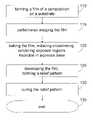
- FIG. 1is a flow chart illustrating a method for preparing a relief pattern on a substrate in an embodiment of the present invention.
- a film of a compositionis formed on a substrate, where the composition may be a blend of two silicon containing polymers and a photosensitive acid generator as described above.
- the filmmay be formed by processes such as spin coating, spray coating, dip coating, doctor blading, and the like, which may be used individually and in combinations thereof in accordance with the methods of the present invention.
- the substratemay comprise materials of the Group I, II, III, and IV elements, plastic material, silicon dioxide, glass, fused silica, mica, ceramic, metals deposited on the aforementioned substrates, combinations thereof, and the like.
- a substratemay comprise a prepared silicon wafer substrate such as those employed in semiconductor manufacturing.
- the filmmay be disposed on top of the substrate or may be integrally joined with the substrate.
- step 115the film is imaged patternwise using a radiation source, resulting in the photosensitive acid generator producing an acid catalyst in the exposed regions of the film.
- FIG. 2is an illustration of patternwise imaging, wherein a radiation source 205 projects radiation through a patterned mask 210 onto a film 225 disposed on a substrate 200 .
- the maskmay have a pattern of masked sections 220 which are substantially opaque to the radiation, and unmasked sections 215 which are substantially transparent to the radiation. Radiation passing through the unmasked sections 215 may be transmitted to the film 225 to be absorbed in the exposed regions 230 of the film 225 , wherein the radiation may induce the production of an acid catalyst in the exposed regions 230 of the film 225 .
- Unexposed regions 240may not produce an acid catalyst.
- Exposure to the radiationsuch as ultraviolet (UV) light at a wavelength from about 12 nm to about 1000 nm, electron beam radiation, plasma, etc.
- a post exposure bakemay render the exposed regions 230 insoluble in a developer.
- step 120the film is post exposure baked, which may induce crosslinking in the exposed regions of the film, rendering the exposed regions insoluble in aqueous base.
- Crosslinking of the functional groups (such as silanol end groups) to form interpenetrating latticesmay increase the integrity of the patterned features following UV-thermal treatment while simultaneously producing a low-k insulating material (k ⁇ 3.0).
- the post-exposure bake temperature of step 120may be in the range from about 50° C. to about 200° C.
- the filmis developed and the base soluble unexposed regions of the film may be removed from the film to leave a relief pattern remaining from the exposed, crosslinked regions of the film.
- the developermay be organic or aqueous based, such as an alkaline aqueous developer.
- step 130the relief pattern is cured.
- a final curing step at a processing temperature compatible with back-end-of-line (BEOL) requirementsmay improve the patterned film properties, such as the dielectric constant, without detriment to pattern fidelity.
- Curingmay include thermal treatment of at least 200° C. of the patterned and developed film, such as from about 300° C. to about 450° C. for example. Curing may utilize thermal treatment, UV radiation, electron beam irradiation, plasma, or combinations of these techniques, such as thermal treatment in combination with UV radiation, for example.
- DSCDifferential scanning calorimetry
- GPCgel permeation chromatography
- THFtetrahydrofuran
- IR spectrawere recorded on a Nicolet 510 FT-IR spectrometer on a film cast on a KBr plate. Film thickness was measured on a Tencor alpha-step 2000.
- a quartz crystal microbalance (QCM)was used to study the dissolution kinetics of the resist films in an aqueous tetramethylammonium hydroxide (TMAH) solution (CD-26). Modulus and hardness data were acquired using a nanoindentation method. Nanoindentation was performed with a Nano Intender XP system (Nano Instruments Innovation Center), equipped with the Dynamic Contact Module (DCM). The DCM may provide an overall miniaturization of the XP system, which may make it more suitable to perform indentations in low force ranges, such as 0.01 millinewtons (mN) to 12 mN). The DCM machine used a Berkovitch indenter (angle 65.3°). The Continuous Stiffness Measurement (CSM) option was used.
- TMAHaqueous tetramethylammonium hydroxide
- the cooling bathwas removed and the mixture was allowed to warm to room temperature and stir for about 20 hours.
- the reaction mixturewas placed in a separatory funnel and the lower layer was separated and retained.
- the upper layerwas diluted with about 900 milliliters (ml) deionized water and extracted three times with about 450 ml of diethyl ether.
- the ether extractswere combined with the lower layer retained from the first separation and the ether solution washed four times with about 400 ml of about 2% aqueous hydrochloric acid, and three times with about 300 ml of saturated aqueous NaCl (brine).
- the ether solutionwas dried over anhydrous magnesium sulfate, filtered, and evaporated to yield 264.4 g of a hard foam product after drying under high vacuum to constant weight.
- a 260 g portion of the dry foamwas dissolved in about 260 g of toluene, heated to about 100° C. with stirring, 20 drops of about 50% w/w aqueous potassium hydroxide added, and the mixture heated to reflux under nitrogen while collecting azeotroped water in a Dean-Stark trap. After refluxing the reaction mixture for about 36 hours, the reaction temperature had increased from about 103.8° C. to about 110.4° C. GPC analysis of an aliquot taken from the reaction mixture indicated that the molecular weight was in the range of about 3,000 to about 3,500 grams/mole (g/mol).
- reaction mixturewas cooled and precipitated in about 10 liters of stirred hexanes, collected on a filter funnel and washed with 3 ⁇ 500 ml of hexanes. After drying to constant weight, about 220 g of solid was obtained.
- the solid abovewas added portion-wise to a stirred mixture of 140 ml of aqueous ammonium hydroxide (12.4 N) in 1120 ml of methanol at about 50° C.
- the suspensionwas heated to reflux and became homogenous after about 20 minutes at reflux.
- the solutionwas refluxed for about 3 additional hours.
- the reaction solutionwas then cooled to about room temperature, and the polymer product was isolated by precipitation in a mixture of about 128.9 g of acetic acid and about 20 liters of deionized water.
- the solid productwas isolated by filtration and washed with three approximately 1 liter portions of deionized water. Drying in a vacuum oven for several days at about 60° C. yielded 179 g of poly(HMBS/MBS) product.
- a mixture of 1-trichlorosilyl-1-(4-acetoxyphenyl)-ethane (223.2 g; 0.75 mole), 1-trichlorosilyl-1-phenyl-ethane (125.8 g; 0.525.1 mole), and 389 g of anhydrous tetrahydrofuranwere added drop-wise to a rapidly stirred mixture of triethylamine (307.7 g; 4.2075 mole) and 389 g of deionized water while cooling with an ice bath to maintain the reaction temperature between about 0° C. and about 10° C. After the addition was complete, the mixture was stirred at a temperature between about 0° C. and about 10° C., for one hour.
- the cooling bathwas removed and the mixture was allowed to warm to room temperature and stir for about 20 hours.
- the reaction mixturewas placed in a separatory funnel and the lower layer was separated and retained.
- the upper layerwas diluted with about 900 ml deionized water and extracted three times with about 450 ml of diethyl ether.
- the ether extractswere combined with the lower layer retained from the first separation and the ether solution washed four times with about 400 ml of about 2% aqueous hydrochloric acid, and four times with 400 ml of deionized water.
- the ether solutionwas evaporated to yield 261.0 g of a hard foam product after pumping under high vacuum to constant weight over several days.
- a 100 g portion of the dry foam product abovewas dissolved in 100 g of toluene, along with 1.15 grams of a 40% w/w aqueous solution of tetrabutyl ammonium hydroxide, and was heated to reflux under nitrogen while collecting azeotroped water in a Dean-Stark trap. After refluxing the reaction mixture for about 36 hours, the reaction temperature had increased to 110.8° C. GPC of an aliquot taken from the reaction mixture indicated that the molecular weight was between about 3,000 to about 3,500 g/mol. The reaction mixture was cooled and precipitated in about 3.5 liters of stirred hexane, collected on a filter funnel and washed with three times with about 300 ml of hexanes. After drying to constant weight, approximately 81 g of solid was obtained.
- the resulting solidwas re-suspended in a mixture of about 3.7 liters of deionized water and about 30 grams of acetic acid, and then filtered, where this process of re-suspending and filtering was repeated three times.
- the solidwas then re-suspended in about 3.7 liters of deionized water for about 4 hours and then filtered, where this process of re-suspending and filtering was repeated three times. Drying the product in a vacuum oven for several days at about 60° C. yielded about 73.6 g of poly(HMBS/MBS) product.
- a patternable low-k compositionwas formulated with 60 g of a 20 wt % solution of 6:4 pHMBS/MBS in propylene glycol monomethyl ether acetate (PGMEA), 40 g of a 20 wt % solution of the silsesquioxane copolymer LKD-2021, 2 g of a 20 wt % solution of triphenylsulfonium nonaflate in PGMEA, and 2 g of a 0.5 wt % solution of an organic base such as trioctylamine in PGMEA.
- the resulting patternable low-k formulationwas filtered through a 0.2 micron ( ⁇ m) filter.
- the patternable low-k compositionwas spin coated (30 seconds at 2000 rpm) onto an 8 inch silicon wafer to produce an approximately 0.6 ⁇ m film.
- the wafer and filmwere pre-exposure baked at about 110° C. for about 60 seconds (s), pattern-wise exposed to 248 nm deep ultraviolet (DUV) light on an ASML (0.63 NA, 5/8 annular) DUV stepper, and then post exposure baked at 110° C. for 60 s. This was followed by two 30 s puddle development steps with 0.26 N TMAH developer to resolve 0.250 ⁇ m line and space features at a radiant energy dose of 26 millijoules/cm 2 (mj/cm 2 ).
- FIG. 3Ais a scanning electron microscope (SEM) image of a 250 nm line pattern 310 created in a film 303 on a substrate 300 as described above in example 3.
- FIG. 3Bis an SEM image of a 250 nm line pattern 320 created in a film 323 on a substrate 300 as described above in example 3, after the pattern has undergone a UV-thermal cure at 400° C. for 10 minutes, showing no loss in pattern fidelity as compared with the image of FIG. 3A .
- SEMscanning electron microscope
- a patternable low-k compositionwas formulated with 60 g of a 20 wt % solution of 6:4 pHMBS/MBS in PGMEA, 40 g of a 20 wt % solution of the silsesquioxane copolymer LKD-2021, 2 g of a 20 wt % solution of triphenylsulfonium nonaflate in PGMEA, and 2 g of a 0.5 wt % solution of a base such as trioctylamine in PGMEA.
- the resulting patternable low-k formulationwas filtered through a 0.2 ⁇ m filter.
- the patternable low-k compositionwas spin coated onto an 8 inch silicon wafer and pre-exposure baked at about 110° C. for 60 s, pattern-wise exposed to 248 nm DUV light on an ASML (0.63 NA, 5/8 annular) DUV stepper, and post-exposure baked at about 110° C. for 60 s. This was followed by two 30 s puddle development steps at 12 mJ/cm 2 with 0.26 N TMAH developer to resolve 0.20 ⁇ m contact hole features. The contact hole pattern was subjected to a UV-thermal cure at 400° C. for 10 min. under a N 2 atmosphere. The resultant cured film exhibited no loss of pattern fidelity.
- FIG. 4Ais an SEM image of 0.20 ⁇ m contact holes 405 in a film 400 prepared as in example 4 above.
- FIG. 4Bis an SEM image of 0.20 ⁇ m contact holes 415 in a film 410 prepared as in example 4 above, after the sample has undergone a UV-thermal cure at 400° C. for 10 minutes, showing no loss in pattern fidelity as compared with the image of FIG. 4A .
- a patternable low-k compositionwas formulated with 60 g of a 20 wt % solution of 6:4 pHMBS/MBS in PGMEA, 40 g of a 20 wt % solution of the silsesquioxane copolymer LKD-2056, 2 g of a 20 wt % solution of triphenylsulfonium nonaflate in PGMEA, and 2 g of a 0.5 wt % solution of a base such as trioctylamine in PGMEA.
- the resulting patternable low-k formulationwas filtered through a 0.2 ⁇ m filter.
- the patternable low-k compositionwas spin coated onto an 8 inch silicon wafer and pre-exposure baked at 110° C. for 60 s, patternwise exposed to 248 nm DUV light on an ASML (0.63 NA, 5/8 annular) DUV stepper, and post exposure baked at 110° C. for 60 s. This was followed by two 30 s puddle development steps with 0.26 N TMAH developer to resolve 0.20 ⁇ m line and space features.
- the patterned arraywas subjected to a UV-thermal cure at 400° C. for 10 min. under a N 2 atmosphere. The resultant cured film exhibited no loss of pattern fidelity.
- the 250 nm line and space features in example 3 and 200 mm contact hole features in example 4were subjected to a UV-thermal cure at 400° C. for 10 min under a N 2 atmosphere in an 8 inch Applied Materials Producer broadband UV cure tool and showed no loss in pattern fidelity.
- the resultant UV cured blanket film of the formulation in examples 3 and 4had a dielectric constant of 2.63 and 2.59 measured by 4 point probe method with a metal-on-semiconductor structure at 23° C. and 150° C., respectively.
- the resultant UV cured blanket film of the formulation in examples 3 and 4had a modulus of 3.4 gigapascals (GPa), a hardness of 0.37 GPa as measured by a nanoindentation method, a films stress of 45 MPa by a wafer bending method and a crack growth rate of 3.5 ⁇ 10 ⁇ 10 m/sec in water.
Landscapes
- Engineering & Computer Science (AREA)
- Physics & Mathematics (AREA)
- General Physics & Mathematics (AREA)
- Condensed Matter Physics & Semiconductors (AREA)
- Manufacturing & Machinery (AREA)
- Computer Hardware Design (AREA)
- Microelectronics & Electronic Packaging (AREA)
- Power Engineering (AREA)
- Spectroscopy & Molecular Physics (AREA)
- Plasma & Fusion (AREA)
- Materials For Photolithography (AREA)
- Compositions Of Macromolecular Compounds (AREA)
Abstract
Description
- The invention relates generally to on-chip electrical insulators used in integrated circuits, and more specifically, silicon-containing polymer blends as photopatternable dielectric materials.
- The continuous shrinking in dimensions of electronic devices utilized in ultra-large scale semiconductor integrated (ULSI) circuits in recent years may have resulted in increasing the resistance of the back-end-of-the-line (BEOL) metallization without concomitantly decreasing the interconnect capacitances. Interconnects may be scaled to higher aspect ratios (a height to width ratio of typically greater than 3:1) to mitigate the resistance increases, which may lead to increased capacitances. This combined effect may increase signal delays in ULSI electronic devices.
- The materials may be patterned by several patterning and sacrificial masking materials which may include photoresist polymers, via fill materials. Following the lithographic patterning of the masking layer, a series of etching steps may be employed to transfer the pattern from the photoresist to each of the layers underneath, including the insulating layer. The patterning of insulating materials may require as many as seven layers, some of which may be removed after patterning, resulting in a complex and inefficient process.
- It would thus be highly desirable to provide a material which can reduce the integration complexity and processing steps required, and does not require costly photoresist polymers and/or significantly reduces etching processes.
- The present invention relates to a composition comprising:
- a polymer blend comprising a first polymer and a second polymer, wherein said first polymer is described by the general formula:
- wherein, m and n are integers greater than zero, R2is a group containing at least one carbon atom, wherein R1is selected from the group consisting of
- wherein said second polymer is described by the general formula:
- wherein x is an integer greater than zero and R3is a carbon functional group comprising at least one carbon atom, wherein said second polymer is configured to undergo chemical crosslinking upon sufficient exposure to light, thermal energy, or a combination thereof; and
- a photosensitive acid generator.
- The present invention relates to a method of forming a relief pattern on a substrate, comprising:
- forming a film of the composition of claim1 on the substrate;
- patternwise imaging said film through a mask, wherein at least one region of said film is exposed to radiation, resulting in production of an acid catalyst in said at least one exposed region of said film;
- after said imaging, baking said film, resulting in inducing crosslinking in said at least one exposed region of said film, wherein said crosslinking renders said exposed region insoluble in aqueous base;
- after said baking, developing said film in an aqueous base solution, resulting in removal of base-soluble unexposed regions of said film, wherein a relief pattern from said film remains following said removal; and
- curing said relief pattern.
- The present invention relates to a composition, comprising:
- a polymer blend comprising a first silsesquioxane polymer and a second silsesquioxane polymer, wherein said first silsesquioxane polymer is described by the general formula:
- where m and n are integers in a range from about 1 to about 5000, R1is
- wherein said second silsesquioxane polymer is described by the general formula:
- where x is an integer in a range from about 4 to about 50,000, and where R3is a methyl group, wherein said second silsesquioxane polymer comprises end groups configured to undergo photo-acid catalyzed condensation reactions upon sufficient exposure to light, thermal energy, or a combination thereof;
- an organic base; and
- a photosensitive acid generator.
- The features of the invention are set forth in the appended claims. The invention itself, however, will be best understood by reference to the following detailed description of illustrative embodiments when read in conjunction with the accompanying drawings.
FIG. 1 is a flow chart illustrating a method for preparing a relief pattern, in accordance with embodiments of the present invention.FIG. 2 is an illustration of patternwise imaging, in accordance with embodiments of the present invention.FIG. 3A is a scanning electron microscope (SEM) image of a 250 nanometer (nm) line pattern, in accordance with embodiments of the present invention.FIG. 3B is an SEM image of a 250 nm line pattern after ultraviolet-thermal curing, in accordance with embodiments of the present invention.FIG. 4A is an SEM image of 0.20 μm contact holes in a film, in accordance with embodiments of the present invention.FIG. 4B is an SEM image of 0.20 μm contact holes in a film after ultraviolet-thermal curing, in accordance with embodiments of the present invention.- Although certain embodiments of the present invention will be shown and described in detail, it should be understood that various changes and modifications may be made without departing from the scope of the appended claims. The scope of the present invention will in no way be limited to the number of constituting components, the materials thereof, the shapes thereof, the relative arrangement thereof, etc., and are disclosed simply as examples of embodiments. The features and advantages of the present invention are illustrated in detail in the accompanying drawings, wherein like reference numerals refer to like elements throughout the drawings. Although the drawings are intended to illustrate the present invention, the drawings are not necessarily drawn to scale.
- An embodiment of the present invention comprises a polymer blend as a photopatternable composition having a low dielectric constant (k). The composition may be used for on-chip electrical insulators and for forming relief patterns for on-chip interconnects such as those used in integrated circuits, for example. Unless otherwise specified the dielectric constants mentioned herein are measured relative to that of vacuum. The term “low-k” denotes a dielectric material having a dielectric constant that is less than 4.0. The blend composition may be comprised of at least two aqueous base soluble, silicon-containing polymers. At least one of the polymers may provide control over the rate of dissolution in aqueous base. Blending of materials may allow properties such as dissolution rate and aqueous base solubility to be appropriately adjusted. A second blend component may be a silicon-containing polymer which may possess acid-sensitive imageable functional groups (such as silanol end groups, for example) which may undergo condensation reactions in the presence of acid to form Si—O—Si bonds. The silsesquioxane polymers in the present invention may undergo photo-acid catalyzed crosslinking, thermally induced crosslinking, or a combination of these, such as condensation of silanol end groups, for example. The silicon-containing polymers may comprise organosilicates, silsesquioxanes, siloxane, and the like, and may be soluble in aqueous base or organic solvents.
- One embodiment of the present invention may comprise a polymer blend of silsesquioxane polymers. The polymers in the blend may be miscible with each other. The first silsesquioxane polymer may be linear, branched, caged compound or combinations thereof having the following general structural formula:
- where, m and n represent the number of repeating units, R1represents a group which may comprise one or more functional groups which may provide polymer solubility in aqueous base, and R2represents a group which may comprise a carbon functionality which may control polymer dissolution in aqueous base. Subscripts m and n may be integers in the range from 0 to about 5000, such as 1 to about 5000 for example. R1may not be the same as R2.
- R1is not limited to any specific functional group, and may comprise functional groups which are substituted with —OH groups, —C(O)OH groups, —F, or combinations thereof. R1may comprise linear or branched alkyls, cycloalkyls, aromatics, arenes, or acrylics. For example, R1may be
- R2is not necessarily limited to any specific functional group, and may comprise linear or branched alkyls, cylcoalkyls, aromatics, arenes, acrylates, or combinations thereof. For example R2may be:
- The R1and R2proportions and structures may be selected to provide a material suitable for photolithographic patterning processes.
- The second silsesquioxane polymer may comprise a polymer having the structural formula:
- wherein R3may be a functional group comprising alkyls, cycloalkyls, aryl, or combinations thereof, and wherein x represents the number of repeating units and may be an integer in a range from 4 to 50000. For example, R3may be:
- In one embodiment, the second silsesquioxane polymer may be poly(methylsilsesquioxane), where R3is a methyl group, and x is an integer from about 4 to about 1,000. In another embodiment, x may be greater than 1,000. The second silsesquioxane polymer may comprise a copolymer. The second silsesquioxane polymer structure may be caged, linear, branched, or combinations thereof. The silsesquioxane polymers of the present invention may comprise end groups comprising silanols, halosilanes, acetoxysilanes, silylamines, alkoxysilanes, and combinations thereof, which may undergo condensation reactions in the presence of an acid generated by a photoacid generator under sufficient exposure to radiation, followed by thermal baking at sufficient temperature, which may result in polymer crosslinking. Polymer molecules of the second polymer may undergo crosslinking with molecules of the first polymer, the second polymer, or a combination of these. In one embodiment of the present invention, the second silsesquioxane may be the methylsilsesquioxane polymer LKD 2021 or LKD-2056 (products of JSR Corporation) which contains silanol end groups.
- The silsesquioxane polymers in the polymer blend may have a weight averaged molecular weight in the range from about 200 to about 5,000,000 g/mol, such as from about 1500 to about 10,000 g/mol, for example.
- In one embodiment of the present invention, the composition comprising the polymer blend may further comprise a photosensitive acid generator (PAG) blended with the two blended polymers. The photosensitive acid generator may be miscible with the two polymers. Examples of some PAGs may comprise: (trifluoro-methylsulfonyloxy)-bicyclo[2.2.1]hept-5-ene-2,3-dicarboximide (MDT), N-hydroxy-naphthalimide (DDSN), onium salts, aromatic diazonium salts, sulfonium salts, diaryliodonium salts, and sulfonic acid esters of N-hydroxyamides, imides, or combinations thereof.
- The concentrations of each of the silsesquioxane polymers in the blend formulation may be from about 1 to about 99% weight/weight (w/w) of the total polymer composition, for example, the concentration of the second silsesquioxane polymer may be from about 5% to about 95% of the total polymer composition. In one embodiment of the invention, the concentration of the acid sensitive polymer may be about 20% to about 80% w/w of the total polymer composition. In another embodiment, the composition of the acid sensitive polymer may be about 30% to about 60% w/w of the total polymer composition.
- The composition of the present invention may further comprise an organic crosslinking agent, such as methylphenyltetramethoxymethyl glycouril (methylphenyl POWDERLINK), tetramethoxymethyl glycouril, methylpropyltetramethoxymethyl glycouril, or 2,6-bis(hydroxymethyl)-p-cresol. Photobase generators may also be used, within the scope of the present invention, for crosslinking silanol polymers. The photopatternable low-k composition of the present invention may further comprise a casting solvent to dissolve the other components. The casting solvent may be used to prepare a film of the composition. Suitable casting solvents may comprise solvents such as ethoxyethylpropionate (EEP), a combination of EEP and γ-butyrolactone, propylene-glycol monomethylether alcohol and acetate, propyleneglycol monopropyl alcohol and acetate, ethyl lactate, or combinations thereof.
- In optimizing the photolithography process, the composition may further comprise an organic base. The base may be any suitable base known in the resist art. Examples of bases include tetraalkylammonium hydroxides, cetyltrimethylammonium hydroxide, 1,8-diaminonaphthalene, or a combination of these The compositions of the present invention are not limited to any specific selection of base.
FIG. 1 is a flow chart illustrating a method for preparing a relief pattern on a substrate in an embodiment of the present invention. Instep 110, a film of a composition is formed on a substrate, where the composition may be a blend of two silicon containing polymers and a photosensitive acid generator as described above. The film may be formed by processes such as spin coating, spray coating, dip coating, doctor blading, and the like, which may be used individually and in combinations thereof in accordance with the methods of the present invention. The substrate may comprise materials of the Group I, II, III, and IV elements, plastic material, silicon dioxide, glass, fused silica, mica, ceramic, metals deposited on the aforementioned substrates, combinations thereof, and the like. For example, a substrate may comprise a prepared silicon wafer substrate such as those employed in semiconductor manufacturing. The film may be disposed on top of the substrate or may be integrally joined with the substrate.- In
step 115, the film is imaged patternwise using a radiation source, resulting in the photosensitive acid generator producing an acid catalyst in the exposed regions of the film. FIG. 2 is an illustration of patternwise imaging, wherein aradiation source 205 projects radiation through apatterned mask 210 onto afilm 225 disposed on asubstrate 200. The mask may have a pattern ofmasked sections 220 which are substantially opaque to the radiation, and unmaskedsections 215 which are substantially transparent to the radiation. Radiation passing through theunmasked sections 215 may be transmitted to thefilm 225 to be absorbed in the exposedregions 230 of thefilm 225, wherein the radiation may induce the production of an acid catalyst in the exposedregions 230 of thefilm 225.Unexposed regions 240 may not produce an acid catalyst. Exposure to the radiation (such as ultraviolet (UV) light at a wavelength from about 12 nm to about 1000 nm, electron beam radiation, plasma, etc.) followed by a post exposure bake may render the exposedregions 230 insoluble in a developer.- Referring again to
FIG. 1 , instep 120, the film is post exposure baked, which may induce crosslinking in the exposed regions of the film, rendering the exposed regions insoluble in aqueous base. Crosslinking of the functional groups (such as silanol end groups) to form interpenetrating lattices may increase the integrity of the patterned features following UV-thermal treatment while simultaneously producing a low-k insulating material (k<3.0). The post-exposure bake temperature ofstep 120 may be in the range from about 50° C. to about 200° C. - In
step 125, the film is developed and the base soluble unexposed regions of the film may be removed from the film to leave a relief pattern remaining from the exposed, crosslinked regions of the film. The developer may be organic or aqueous based, such as an alkaline aqueous developer. - In
step 130, the relief pattern is cured. A final curing step at a processing temperature compatible with back-end-of-line (BEOL) requirements may improve the patterned film properties, such as the dielectric constant, without detriment to pattern fidelity. Curing may include thermal treatment of at least 200° C. of the patterned and developed film, such as from about 300° C. to about 450° C. for example. Curing may utilize thermal treatment, UV radiation, electron beam irradiation, plasma, or combinations of these techniques, such as thermal treatment in combination with UV radiation, for example. The process ends at135. - Where appropriate, the following techniques and equipment were utilized in the examples below:1H and13C NMR spectra were obtained at room temperature on an
Avance 400 spectrometer. Quantitative13C NMR was run at room temperature in acetone-d6in an inverse-gated1H-decoupled mode using Cr(acac)3as a relaxation agent on anAvance 400 spectrometer. For polymer composition analysis19F NMR (379 MHz) spectra were also obtained using aBruker Avance 400 spectrometer. Thermo-gravimetric analysis (TGA) was performed at a heating rate of 5° C./min in N2on a TA Instrument Hi-Res TGA 2950 Thermogravimetric Analyzer. Differential scanning calorimetry (DSC) was performed at a heating rate of 10° C./minute on a TA Instruments DSC 2920 modulated differential scanning calorimeter. Molecular weights were measured using gel permeation chromatography (GPC) in tetrahydrofuran (THF) on a Waters Model 150 chromatograph relative to polystyrene standards. IR spectra were recorded on a Nicolet 510 FT-IR spectrometer on a film cast on a KBr plate. Film thickness was measured on a Tencor alpha-step 2000. A quartz crystal microbalance (QCM) was used to study the dissolution kinetics of the resist films in an aqueous tetramethylammonium hydroxide (TMAH) solution (CD-26). Modulus and hardness data were acquired using a nanoindentation method. Nanoindentation was performed with a Nano Intender XP system (Nano Instruments Innovation Center), equipped with the Dynamic Contact Module (DCM). The DCM may provide an overall miniaturization of the XP system, which may make it more suitable to perform indentations in low force ranges, such as 0.01 millinewtons (mN) to 12 mN). The DCM machine used a Berkovitch indenter (angle 65.3°). The Continuous Stiffness Measurement (CSM) option was used. - (6:4 pHMBS/MBS).
- A mixture of 1-trichlorosilyl-1-(4-acetoxyphenyl)-ethane (223.2 grams; 0.75 mole), 1-trichlorosilyl-1-phenyl-ethane (125.8 grams; 0.525.1 mole), and 389 grams (g) of anhydrous tetrahydrofuran were added drop-wise to a rapidly stirred mixture of triethylamine (307.7 g; 4.2075 mole) and 389 g of deionized water while cooling with an ice bath to maintain the reaction temperature between about 0° C. and about 10° C. After the addition was complete, the mixture was stirred at a temperature between about 0° C. and about 10° C., for one hour. The cooling bath was removed and the mixture was allowed to warm to room temperature and stir for about 20 hours. The reaction mixture was placed in a separatory funnel and the lower layer was separated and retained. The upper layer was diluted with about 900 milliliters (ml) deionized water and extracted three times with about 450 ml of diethyl ether. The ether extracts were combined with the lower layer retained from the first separation and the ether solution washed four times with about 400 ml of about 2% aqueous hydrochloric acid, and three times with about 300 ml of saturated aqueous NaCl (brine). The ether solution was dried over anhydrous magnesium sulfate, filtered, and evaporated to yield 264.4 g of a hard foam product after drying under high vacuum to constant weight.
- A 260 g portion of the dry foam was dissolved in about 260 g of toluene, heated to about 100° C. with stirring, 20 drops of about 50% w/w aqueous potassium hydroxide added, and the mixture heated to reflux under nitrogen while collecting azeotroped water in a Dean-Stark trap. After refluxing the reaction mixture for about 36 hours, the reaction temperature had increased from about 103.8° C. to about 110.4° C. GPC analysis of an aliquot taken from the reaction mixture indicated that the molecular weight was in the range of about 3,000 to about 3,500 grams/mole (g/mol). The reaction mixture was cooled and precipitated in about 10 liters of stirred hexanes, collected on a filter funnel and washed with 3×500 ml of hexanes. After drying to constant weight, about 220 g of solid was obtained.
- The solid above was added portion-wise to a stirred mixture of 140 ml of aqueous ammonium hydroxide (12.4 N) in 1120 ml of methanol at about 50° C. The suspension was heated to reflux and became homogenous after about 20 minutes at reflux. The solution was refluxed for about 3 additional hours. The reaction solution was then cooled to about room temperature, and the polymer product was isolated by precipitation in a mixture of about 128.9 g of acetic acid and about 20 liters of deionized water. The solid product was isolated by filtration and washed with three approximately 1 liter portions of deionized water. Drying in a vacuum oven for several days at about 60° C. yielded 179 g of poly(HMBS/MBS) product.
- (6:4 pHMBS/MBS) (Reduced Ion Content Process)
- A mixture of 1-trichlorosilyl-1-(4-acetoxyphenyl)-ethane (223.2 g; 0.75 mole), 1-trichlorosilyl-1-phenyl-ethane (125.8 g; 0.525.1 mole), and 389 g of anhydrous tetrahydrofuran were added drop-wise to a rapidly stirred mixture of triethylamine (307.7 g; 4.2075 mole) and 389 g of deionized water while cooling with an ice bath to maintain the reaction temperature between about 0° C. and about 10° C. After the addition was complete, the mixture was stirred at a temperature between about 0° C. and about 10° C., for one hour. The cooling bath was removed and the mixture was allowed to warm to room temperature and stir for about 20 hours. The reaction mixture was placed in a separatory funnel and the lower layer was separated and retained. The upper layer was diluted with about 900 ml deionized water and extracted three times with about 450 ml of diethyl ether. The ether extracts were combined with the lower layer retained from the first separation and the ether solution washed four times with about 400 ml of about 2% aqueous hydrochloric acid, and four times with 400 ml of deionized water. The ether solution was evaporated to yield 261.0 g of a hard foam product after pumping under high vacuum to constant weight over several days.
- A 100 g portion of the dry foam product above was dissolved in 100 g of toluene, along with 1.15 grams of a 40% w/w aqueous solution of tetrabutyl ammonium hydroxide, and was heated to reflux under nitrogen while collecting azeotroped water in a Dean-Stark trap. After refluxing the reaction mixture for about 36 hours, the reaction temperature had increased to 110.8° C. GPC of an aliquot taken from the reaction mixture indicated that the molecular weight was between about 3,000 to about 3,500 g/mol. The reaction mixture was cooled and precipitated in about 3.5 liters of stirred hexane, collected on a filter funnel and washed with three times with about 300 ml of hexanes. After drying to constant weight, approximately 81 g of solid was obtained.
- The solid obtained above, and about 9 g from a second lot of the same reaction, was added portion-wise to a stirred mixture of 58 ml of aqueous ammonium hydroxide (12.4 N) in 464 ml of methanol at about 50° C. The suspension was heated to reflux and became homogenous after about 20 min at reflux. The solution was refluxed for an addition 3 hours. The reaction solution was then cooled to about room temperature, and the polymer product was isolated by precipitation in a mixture of about 53.4 g of acetic acid and about 7.4 liters of deionized water. The solid product was isolated by filtration and washed with about three 500 ml portions of deionized water. The resulting solid was re-suspended in a mixture of about 3.7 liters of deionized water and about 30 grams of acetic acid, and then filtered, where this process of re-suspending and filtering was repeated three times. The solid was then re-suspended in about 3.7 liters of deionized water for about 4 hours and then filtered, where this process of re-suspending and filtering was repeated three times. Drying the product in a vacuum oven for several days at about 60° C. yielded about 73.6 g of poly(HMBS/MBS) product.
- A patternable low-k composition was formulated with 60 g of a 20 wt % solution of 6:4 pHMBS/MBS in propylene glycol monomethyl ether acetate (PGMEA), 40 g of a 20 wt % solution of the silsesquioxane copolymer LKD-2021, 2 g of a 20 wt % solution of triphenylsulfonium nonaflate in PGMEA, and 2 g of a 0.5 wt % solution of an organic base such as trioctylamine in PGMEA. The resulting patternable low-k formulation was filtered through a 0.2 micron (μm) filter.
- The patternable low-k composition was spin coated (30 seconds at 2000 rpm) onto an 8 inch silicon wafer to produce an approximately 0.6 μm film. The wafer and film were pre-exposure baked at about 110° C. for about 60 seconds (s), pattern-wise exposed to 248 nm deep ultraviolet (DUV) light on an ASML (0.63 NA, 5/8 annular) DUV stepper, and then post exposure baked at 110° C. for 60 s. This was followed by two 30 s puddle development steps with 0.26 N TMAH developer to resolve 0.250 μm line and space features at a radiant energy dose of 26 millijoules/cm2(mj/cm2).
FIG. 3A is a scanning electron microscope (SEM) image of a 250nm line pattern 310 created in afilm 303 on asubstrate 300 as described above in example 3.FIG. 3B is an SEM image of a 250nm line pattern 320 created in afilm 323 on asubstrate 300 as described above in example 3, after the pattern has undergone a UV-thermal cure at 400° C. for 10 minutes, showing no loss in pattern fidelity as compared with the image ofFIG. 3A .- A patternable low-k composition was formulated with 60 g of a 20 wt % solution of 6:4 pHMBS/MBS in PGMEA, 40 g of a 20 wt % solution of the silsesquioxane copolymer LKD-2021, 2 g of a 20 wt % solution of triphenylsulfonium nonaflate in PGMEA, and 2 g of a 0.5 wt % solution of a base such as trioctylamine in PGMEA. The resulting patternable low-k formulation was filtered through a 0.2 μm filter.
- The patternable low-k composition was spin coated onto an 8 inch silicon wafer and pre-exposure baked at about 110° C. for 60 s, pattern-wise exposed to 248 nm DUV light on an ASML (0.63 NA, 5/8 annular) DUV stepper, and post-exposure baked at about 110° C. for 60 s. This was followed by two 30 s puddle development steps at 12 mJ/cm2with 0.26 N TMAH developer to resolve 0.20 μm contact hole features. The contact hole pattern was subjected to a UV-thermal cure at 400° C. for 10 min. under a N2atmosphere. The resultant cured film exhibited no loss of pattern fidelity.
FIG. 4A is an SEM image of 0.20 μm contact holes 405 in afilm 400 prepared as in example 4 above.FIG. 4B is an SEM image of 0.20 μm contact holes 415 in afilm 410 prepared as in example 4 above, after the sample has undergone a UV-thermal cure at 400° C. for 10 minutes, showing no loss in pattern fidelity as compared with the image ofFIG. 4A .- A patternable low-k composition was formulated with 60 g of a 20 wt % solution of 6:4 pHMBS/MBS in PGMEA, 40 g of a 20 wt % solution of the silsesquioxane copolymer LKD-2056, 2 g of a 20 wt % solution of triphenylsulfonium nonaflate in PGMEA, and 2 g of a 0.5 wt % solution of a base such as trioctylamine in PGMEA. The resulting patternable low-k formulation was filtered through a 0.2 μm filter.
- The patternable low-k composition was spin coated onto an 8 inch silicon wafer and pre-exposure baked at 110° C. for 60 s, patternwise exposed to 248 nm DUV light on an ASML (0.63 NA, 5/8 annular) DUV stepper, and post exposure baked at 110° C. for 60 s. This was followed by two 30 s puddle development steps with 0.26 N TMAH developer to resolve 0.20 μm line and space features. The patterned array was subjected to a UV-thermal cure at 400° C. for 10 min. under a N2atmosphere. The resultant cured film exhibited no loss of pattern fidelity.
- The 250 nm line and space features in example 3 and 200 mm contact hole features in example 4 were subjected to a UV-thermal cure at 400° C. for 10 min under a N2atmosphere in an 8 inch Applied Materials Producer broadband UV cure tool and showed no loss in pattern fidelity. The resultant UV cured blanket film of the formulation in examples 3 and 4 had a dielectric constant of 2.63 and 2.59 measured by 4 point probe method with a metal-on-semiconductor structure at 23° C. and 150° C., respectively.
- The resultant UV cured blanket film of the formulation in examples 3 and 4 had a modulus of 3.4 gigapascals (GPa), a hardness of 0.37 GPa as measured by a nanoindentation method, a films stress of 45 MPa by a wafer bending method and a crack growth rate of 3.5×10⁻¹⁰m/sec in water.
- The foregoing description of the embodiments of this invention has been presented for purposes of illustration and description. It is not intended to be exhaustive or to limit the invention to the precise form disclosed, and obviously, many modifications and variations are possible. Such modifications and variations that may be apparent to a person skilled in the art are intended to be included within the scope of this invention as defined by the accompanying claims.


Claims (3)


Priority Applications (2)
| Application Number | Priority Date | Filing Date | Title |
|---|---|---|---|
| US11/750,356US7867689B2 (en) | 2007-05-18 | 2007-05-18 | Method of use for photopatternable dielectric materials for BEOL applications |
| US12/542,821US8470516B2 (en) | 2007-05-18 | 2009-08-18 | Method of forming a relief pattern by e-beam lithography using chemical amplification, and derived articles |
Applications Claiming Priority (1)
| Application Number | Priority Date | Filing Date | Title |
|---|---|---|---|
| US11/750,356US7867689B2 (en) | 2007-05-18 | 2007-05-18 | Method of use for photopatternable dielectric materials for BEOL applications |
Related Child Applications (1)
| Application Number | Title | Priority Date | Filing Date |
|---|---|---|---|
| US12/542,821Continuation-In-PartUS8470516B2 (en) | 2007-05-18 | 2009-08-18 | Method of forming a relief pattern by e-beam lithography using chemical amplification, and derived articles |
Publications (2)
| Publication Number | Publication Date |
|---|---|
| US20080286467A1true US20080286467A1 (en) | 2008-11-20 |
| US7867689B2 US7867689B2 (en) | 2011-01-11 |
Family
ID=40027779
Family Applications (1)
| Application Number | Title | Priority Date | Filing Date |
|---|---|---|---|
| US11/750,356Expired - Fee RelatedUS7867689B2 (en) | 2007-05-18 | 2007-05-18 | Method of use for photopatternable dielectric materials for BEOL applications |
Country Status (1)
| Country | Link |
|---|---|
| US (1) | US7867689B2 (en) |
Cited By (25)
| Publication number | Priority date | Publication date | Assignee | Title |
|---|---|---|---|---|
| US20100314767A1 (en)* | 2009-06-16 | 2010-12-16 | International Business Machines Corporation | Self-aligned dual damascene beol structures with patternable low- k material and methods of forming same |
| US20100319971A1 (en)* | 2009-06-17 | 2010-12-23 | International Business Machines Corporation | Airgap-containing interconnect structure with improved patternable low-k material and method of fabricating |
| US20110042790A1 (en)* | 2009-08-24 | 2011-02-24 | International Business Machines Corporation | MULTIPLE PATTERNING USING IMPROVED PATTERNABLE LOW-k DIELECTRIC MATERIALS |
| US20110045387A1 (en)* | 2007-05-18 | 2011-02-24 | International Business Machines Corporation | Method of Forming a Relief Pattern by E-Beam Lithography Using Chemical Amplification, and Derived Articles |
| US20110074044A1 (en)* | 2009-09-29 | 2011-03-31 | International Business Machines Corporation | Patternable low-k dielectric interconnect structure with a graded cap layer and method of fabrication |
| US20110115094A1 (en)* | 2009-11-16 | 2011-05-19 | International Business Machines Corporation | STRUCTURES AND METHODS FOR PHOTO-PATTERNABLE LOW-k (PPLK) INTEGRATION |
| US20110115090A1 (en)* | 2009-11-19 | 2011-05-19 | International Business Machines Corporation | Interconnect structure including a modified photoresist as a permanent interconnect dielectric and method of fabricating same |
| US20110260326A1 (en)* | 2010-04-27 | 2011-10-27 | International Business Machines Corporation | Structures and methods for air gap integration |
| WO2011147670A1 (en) | 2010-05-27 | 2011-12-01 | International Business Machines Corporation | Interconnect structure |
| US8232198B2 (en) | 2010-08-05 | 2012-07-31 | International Business Machines Corporation | Self-aligned permanent on-chip interconnect structure formed by pitch splitting |
| US8241992B2 (en) | 2010-05-10 | 2012-08-14 | International Business Machines Corporation | Method for air gap interconnect integration using photo-patternable low k material |
| US20120301980A1 (en)* | 2010-06-22 | 2012-11-29 | International Business Machines Corporation | Methodology for evaluation of electrical characteristics of carbon nanotubes |
| US8354339B2 (en) | 2010-07-20 | 2013-01-15 | International Business Machines Corporation | Methods to form self-aligned permanent on-chip interconnect structures |
| US8449781B2 (en) | 2010-06-22 | 2013-05-28 | International Business Machines Corporation | Selective etch back process for carbon nanotubes intergration |
| US8475667B2 (en) | 2010-06-22 | 2013-07-02 | International Business Machines Corporation | Method of patterning photosensitive material on a substrate containing a latent acid generator |
| US8617941B2 (en) | 2011-01-16 | 2013-12-31 | International Business Machines Corporation | High-speed graphene transistor and method of fabrication by patternable hard mask materials |
| US8642252B2 (en) | 2010-03-10 | 2014-02-04 | International Business Machines Corporation | Methods for fabrication of an air gap-containing interconnect structure |
| US9453109B2 (en) | 2012-12-21 | 2016-09-27 | 3M Innovative Properties Company | Curable silsesquioxane polymers, compositions, articles, and methods |
| US9957416B2 (en) | 2014-09-22 | 2018-05-01 | 3M Innovative Properties Company | Curable end-capped silsesquioxane polymer comprising reactive groups |
| US9957358B2 (en) | 2014-09-22 | 2018-05-01 | 3M Innovative Properties Company | Curable polymers comprising silsesquioxane polymer core silsesquioxane polymer outer layer, and reactive groups |
| US10066123B2 (en) | 2013-12-09 | 2018-09-04 | 3M Innovative Properties Company | Curable silsesquioxane polymers, compositions, articles, and methods |
| US10370564B2 (en) | 2014-06-20 | 2019-08-06 | 3M Innovative Properties Company | Adhesive compositions comprising a silsesquioxane polymer crosslinker, articles and methods |
| US10392538B2 (en) | 2014-06-20 | 2019-08-27 | 3M Innovative Properties Company | Adhesive compositions comprising a silsesquioxane polymer crosslinker, articles and methods |
| US10573687B2 (en) | 2017-10-31 | 2020-02-25 | International Business Machines Corporation | Magnetic random access memory with permanent photo-patternable low-K dielectric |
| US10597557B2 (en) | 2012-12-21 | 2020-03-24 | 3M Innovative Properties Company | Curable silsesquioxane polymers, compositions, articles, and methods |
Families Citing this family (1)
| Publication number | Priority date | Publication date | Assignee | Title |
|---|---|---|---|---|
| US8389663B2 (en) | 2009-10-08 | 2013-03-05 | International Business Machines Corporation | Photo-patternable dielectric materials curable to porous dielectric materials, formulations, precursors and methods of use thereof |
Citations (20)
| Publication number | Priority date | Publication date | Assignee | Title |
|---|---|---|---|---|
| US4371650A (en)* | 1981-03-26 | 1983-02-01 | General Electric Company | Flame retardant polycarbonates |
| US5538818A (en)* | 1992-05-28 | 1996-07-23 | Mitsubishi Denki Kabushiki Kaisha | Reflection Photomask |
| US5789460A (en)* | 1995-02-02 | 1998-08-04 | Dow Corning Asia, Ltd. | Radiation curable compositions |
| US6087064A (en)* | 1998-09-03 | 2000-07-11 | International Business Machines Corporation | Silsesquioxane polymers, method of synthesis, photoresist composition, and multilayer lithographic method |
| US6187505B1 (en)* | 1999-02-02 | 2001-02-13 | International Business Machines Corporation | Radiation sensitive silicon-containing resists |
| US6613834B2 (en)* | 2000-03-29 | 2003-09-02 | Fujitsu Limited | Low dielectric constant film material, film and semiconductor device using such material |
| US6703181B1 (en)* | 1993-03-12 | 2004-03-09 | Kabushiki Kaisha Toshiba | Photosensitive composition having uniform concentration distribution of components and pattern formation method using the same |
| US6743885B2 (en)* | 2001-07-31 | 2004-06-01 | Sumitomo Chemical Company, Limited | Resin composition for intermediate layer of three-layer resist |
| US20040137241A1 (en)* | 2003-01-08 | 2004-07-15 | International Business Machines Corporation | Patternable low dielectric constsnt materials and their use in ULSI interconnection |
| US6967222B2 (en)* | 2001-05-25 | 2005-11-22 | Shipley Company, L.L.C. | Porous optical materials |
| US6992115B2 (en)* | 2002-03-06 | 2006-01-31 | International Business Machines Corporation | Preparation of crosslinked particles from polymers having activatible crosslinking groups |
| US7056840B2 (en)* | 2003-09-30 | 2006-06-06 | International Business Machines Corp. | Direct photo-patterning of nanoporous organosilicates, and method of use |
| US7072565B2 (en)* | 2004-04-14 | 2006-07-04 | Rohm And Haas Electronic Materials Llc | Waveguide compositions and waveguides formed therefrom |
| US7072563B2 (en)* | 2003-11-25 | 2006-07-04 | Rohm And Haas Electronic Materials Llc | Waveguide compositions and waveguides formed therefrom |
| US7261992B2 (en)* | 2000-12-21 | 2007-08-28 | International Business Machines Corporation | Fluorinated silsesquioxane polymers and use thereof in lithographic photoresist compositions |
| US7261994B2 (en)* | 2004-03-30 | 2007-08-28 | Tokyo Ohka Kogyo Co., Ltd. | Positive resist composition |
| US7318992B2 (en)* | 2004-03-31 | 2008-01-15 | Tokyo Ohka Kogyo Co., Ltd. | Lift-off positive resist composition |
| US7355384B2 (en)* | 2004-04-08 | 2008-04-08 | International Business Machines Corporation | Apparatus, method, and computer program product for monitoring and controlling a microcomputer using a single existing pin |
| US7361444B1 (en)* | 1998-02-23 | 2008-04-22 | International Business Machines Corporation | Multilayered resist systems using tuned polymer films as underlayers and methods of fabrication thereof |
| US7399581B2 (en)* | 2005-02-24 | 2008-07-15 | International Business Machines Corporation | Photoresist topcoat for a photolithographic process |
Family Cites Families (4)
| Publication number | Priority date | Publication date | Assignee | Title |
|---|---|---|---|---|
| US4371605A (en) | 1980-12-09 | 1983-02-01 | E. I. Du Pont De Nemours And Company | Photopolymerizable compositions containing N-hydroxyamide and N-hydroxyimide sulfonates |
| US7507783B2 (en) | 2003-02-24 | 2009-03-24 | Brewer Science Inc. | Thermally curable middle layer comprising polyhedral oligomeric silsesouioxanes for 193-nm trilayer resist process |
| EP1643307A4 (en) | 2003-06-11 | 2009-12-23 | Tokyo Ohka Kogyo Co Ltd | Positive resist composition, resist laminates and process for the formation of resist patterns |
| JP4494061B2 (en) | 2004-03-30 | 2010-06-30 | 東京応化工業株式会社 | Positive resist composition |
- 2007
- 2007-05-18USUS11/750,356patent/US7867689B2/ennot_activeExpired - Fee Related
Patent Citations (22)
| Publication number | Priority date | Publication date | Assignee | Title |
|---|---|---|---|---|
| US4371650A (en)* | 1981-03-26 | 1983-02-01 | General Electric Company | Flame retardant polycarbonates |
| US5538818A (en)* | 1992-05-28 | 1996-07-23 | Mitsubishi Denki Kabushiki Kaisha | Reflection Photomask |
| US6703181B1 (en)* | 1993-03-12 | 2004-03-09 | Kabushiki Kaisha Toshiba | Photosensitive composition having uniform concentration distribution of components and pattern formation method using the same |
| US5789460A (en)* | 1995-02-02 | 1998-08-04 | Dow Corning Asia, Ltd. | Radiation curable compositions |
| US7361444B1 (en)* | 1998-02-23 | 2008-04-22 | International Business Machines Corporation | Multilayered resist systems using tuned polymer films as underlayers and methods of fabrication thereof |
| US6087064A (en)* | 1998-09-03 | 2000-07-11 | International Business Machines Corporation | Silsesquioxane polymers, method of synthesis, photoresist composition, and multilayer lithographic method |
| US6187505B1 (en)* | 1999-02-02 | 2001-02-13 | International Business Machines Corporation | Radiation sensitive silicon-containing resists |
| US6613834B2 (en)* | 2000-03-29 | 2003-09-02 | Fujitsu Limited | Low dielectric constant film material, film and semiconductor device using such material |
| US7261992B2 (en)* | 2000-12-21 | 2007-08-28 | International Business Machines Corporation | Fluorinated silsesquioxane polymers and use thereof in lithographic photoresist compositions |
| US6967222B2 (en)* | 2001-05-25 | 2005-11-22 | Shipley Company, L.L.C. | Porous optical materials |
| US6743885B2 (en)* | 2001-07-31 | 2004-06-01 | Sumitomo Chemical Company, Limited | Resin composition for intermediate layer of three-layer resist |
| US6992115B2 (en)* | 2002-03-06 | 2006-01-31 | International Business Machines Corporation | Preparation of crosslinked particles from polymers having activatible crosslinking groups |
| US20060105181A1 (en)* | 2003-01-08 | 2006-05-18 | International Business Machines Corporation | Patternable low dielectric constant materials and their use in ULSI interconnection |
| US7041748B2 (en)* | 2003-01-08 | 2006-05-09 | International Business Machines Corporation | Patternable low dielectric constant materials and their use in ULSI interconnection |
| US20040137241A1 (en)* | 2003-01-08 | 2004-07-15 | International Business Machines Corporation | Patternable low dielectric constsnt materials and their use in ULSI interconnection |
| US7056840B2 (en)* | 2003-09-30 | 2006-06-06 | International Business Machines Corp. | Direct photo-patterning of nanoporous organosilicates, and method of use |
| US7072563B2 (en)* | 2003-11-25 | 2006-07-04 | Rohm And Haas Electronic Materials Llc | Waveguide compositions and waveguides formed therefrom |
| US7261994B2 (en)* | 2004-03-30 | 2007-08-28 | Tokyo Ohka Kogyo Co., Ltd. | Positive resist composition |
| US7318992B2 (en)* | 2004-03-31 | 2008-01-15 | Tokyo Ohka Kogyo Co., Ltd. | Lift-off positive resist composition |
| US7355384B2 (en)* | 2004-04-08 | 2008-04-08 | International Business Machines Corporation | Apparatus, method, and computer program product for monitoring and controlling a microcomputer using a single existing pin |
| US7072565B2 (en)* | 2004-04-14 | 2006-07-04 | Rohm And Haas Electronic Materials Llc | Waveguide compositions and waveguides formed therefrom |
| US7399581B2 (en)* | 2005-02-24 | 2008-07-15 | International Business Machines Corporation | Photoresist topcoat for a photolithographic process |
Cited By (49)
| Publication number | Priority date | Publication date | Assignee | Title |
|---|---|---|---|---|
| US20110045387A1 (en)* | 2007-05-18 | 2011-02-24 | International Business Machines Corporation | Method of Forming a Relief Pattern by E-Beam Lithography Using Chemical Amplification, and Derived Articles |
| US8470516B2 (en) | 2007-05-18 | 2013-06-25 | International Business Machines Corporation | Method of forming a relief pattern by e-beam lithography using chemical amplification, and derived articles |
| US20100314767A1 (en)* | 2009-06-16 | 2010-12-16 | International Business Machines Corporation | Self-aligned dual damascene beol structures with patternable low- k material and methods of forming same |
| US8415248B2 (en) | 2009-06-16 | 2013-04-09 | International Business Machines Corporation | Self-aligned dual damascene BEOL structures with patternable low-k material and methods of forming same |
| US8519540B2 (en) | 2009-06-16 | 2013-08-27 | International Business Machines Corporation | Self-aligned dual damascene BEOL structures with patternable low- K material and methods of forming same |
| US8659115B2 (en) | 2009-06-17 | 2014-02-25 | International Business Machines Corporation | Airgap-containing interconnect structure with improved patternable low-K material and method of fabricating |
| US20100319971A1 (en)* | 2009-06-17 | 2010-12-23 | International Business Machines Corporation | Airgap-containing interconnect structure with improved patternable low-k material and method of fabricating |
| US20110042790A1 (en)* | 2009-08-24 | 2011-02-24 | International Business Machines Corporation | MULTIPLE PATTERNING USING IMPROVED PATTERNABLE LOW-k DIELECTRIC MATERIALS |
| US8487411B2 (en) | 2009-08-24 | 2013-07-16 | International Business Machines Corporation | Multiple patterning using improved patternable low-κ dielectric materials |
| US8163658B2 (en) | 2009-08-24 | 2012-04-24 | International Business Machines Corporation | Multiple patterning using improved patternable low-k dielectric materials |
| US20110074044A1 (en)* | 2009-09-29 | 2011-03-31 | International Business Machines Corporation | Patternable low-k dielectric interconnect structure with a graded cap layer and method of fabrication |
| WO2011038995A1 (en) | 2009-09-29 | 2011-04-07 | International Business Machines Corporation | Patternable low-k dielectric interconnect structure with a graded cap layer and method of fabrication |
| US8202783B2 (en) | 2009-09-29 | 2012-06-19 | International Business Machines Corporation | Patternable low-k dielectric interconnect structure with a graded cap layer and method of fabrication |
| US8461039B2 (en) | 2009-09-29 | 2013-06-11 | International Business Machines Corporation | Patternable low-K dielectric interconnect structure with a graded cap layer and method of fabrication |
| US9059249B2 (en) | 2009-11-16 | 2015-06-16 | International Business Machines Corporation | Interconnect structures containing a photo-patternable low-k dielectric with a curved sidewall surface |
| US8637395B2 (en) | 2009-11-16 | 2014-01-28 | International Business Machines Corporation | Methods for photo-patternable low-k (PPLK) integration with curing after pattern transfer |
| US20110115094A1 (en)* | 2009-11-16 | 2011-05-19 | International Business Machines Corporation | STRUCTURES AND METHODS FOR PHOTO-PATTERNABLE LOW-k (PPLK) INTEGRATION |
| US20110115090A1 (en)* | 2009-11-19 | 2011-05-19 | International Business Machines Corporation | Interconnect structure including a modified photoresist as a permanent interconnect dielectric and method of fabricating same |
| US8367540B2 (en) | 2009-11-19 | 2013-02-05 | International Business Machines Corporation | Interconnect structure including a modified photoresist as a permanent interconnect dielectric and method of fabricating same |
| US9431295B2 (en) | 2009-11-19 | 2016-08-30 | Globalfoundries Inc. | Interconnect structure including a modified photoresist as a permanent interconnect dielectric and method of fabricating same |
| US8952539B2 (en) | 2010-03-10 | 2015-02-10 | International Business Machines Corporation | Methods for fabrication of an air gap-containing interconnect structure |
| US8642252B2 (en) | 2010-03-10 | 2014-02-04 | International Business Machines Corporation | Methods for fabrication of an air gap-containing interconnect structure |
| US20110260326A1 (en)* | 2010-04-27 | 2011-10-27 | International Business Machines Corporation | Structures and methods for air gap integration |
| US8896120B2 (en)* | 2010-04-27 | 2014-11-25 | International Business Machines Corporation | Structures and methods for air gap integration |
| US8241992B2 (en) | 2010-05-10 | 2012-08-14 | International Business Machines Corporation | Method for air gap interconnect integration using photo-patternable low k material |
| US8629561B2 (en) | 2010-05-10 | 2014-01-14 | International Business Machines Corporation | Air gap-containing interconnect structure having photo-patternable low k material |
| WO2011147670A1 (en) | 2010-05-27 | 2011-12-01 | International Business Machines Corporation | Interconnect structure |
| US8373271B2 (en) | 2010-05-27 | 2013-02-12 | International Business Machines Corporation | Interconnect structure with an oxygen-doped SiC antireflective coating and method of fabrication |
| US8475667B2 (en) | 2010-06-22 | 2013-07-02 | International Business Machines Corporation | Method of patterning photosensitive material on a substrate containing a latent acid generator |
| US8449781B2 (en) | 2010-06-22 | 2013-05-28 | International Business Machines Corporation | Selective etch back process for carbon nanotubes intergration |
| US20120301980A1 (en)* | 2010-06-22 | 2012-11-29 | International Business Machines Corporation | Methodology for evaluation of electrical characteristics of carbon nanotubes |
| US8828749B2 (en)* | 2010-06-22 | 2014-09-09 | International Business Machines Corporation | Methodology for evaluation of electrical characteristics of carbon nanotubes |
| US8853856B2 (en) | 2010-06-22 | 2014-10-07 | International Business Machines Corporation | Methodology for evaluation of electrical characteristics of carbon nanotubes |
| US9196523B2 (en) | 2010-07-20 | 2015-11-24 | Globalfoundries Inc. | Self-aligned permanent on-chip interconnect structures |
| US8354339B2 (en) | 2010-07-20 | 2013-01-15 | International Business Machines Corporation | Methods to form self-aligned permanent on-chip interconnect structures |
| US8795556B2 (en)* | 2010-08-05 | 2014-08-05 | International Business Machines Corporation | Self-aligned permanent on-chip interconnect structure formed by pitch splitting |
| US8232198B2 (en) | 2010-08-05 | 2012-07-31 | International Business Machines Corporation | Self-aligned permanent on-chip interconnect structure formed by pitch splitting |
| US20120205818A1 (en)* | 2010-08-05 | 2012-08-16 | International Business Machines Corporation | Self-aligned permanent on-chip interconnect structure formed by pitch splitting |
| US8617941B2 (en) | 2011-01-16 | 2013-12-31 | International Business Machines Corporation | High-speed graphene transistor and method of fabrication by patternable hard mask materials |
| US9453109B2 (en) | 2012-12-21 | 2016-09-27 | 3M Innovative Properties Company | Curable silsesquioxane polymers, compositions, articles, and methods |
| US10597557B2 (en) | 2012-12-21 | 2020-03-24 | 3M Innovative Properties Company | Curable silsesquioxane polymers, compositions, articles, and methods |
| US10066123B2 (en) | 2013-12-09 | 2018-09-04 | 3M Innovative Properties Company | Curable silsesquioxane polymers, compositions, articles, and methods |
| US10370564B2 (en) | 2014-06-20 | 2019-08-06 | 3M Innovative Properties Company | Adhesive compositions comprising a silsesquioxane polymer crosslinker, articles and methods |
| US10392538B2 (en) | 2014-06-20 | 2019-08-27 | 3M Innovative Properties Company | Adhesive compositions comprising a silsesquioxane polymer crosslinker, articles and methods |
| US9957358B2 (en) | 2014-09-22 | 2018-05-01 | 3M Innovative Properties Company | Curable polymers comprising silsesquioxane polymer core silsesquioxane polymer outer layer, and reactive groups |
| US9957416B2 (en) | 2014-09-22 | 2018-05-01 | 3M Innovative Properties Company | Curable end-capped silsesquioxane polymer comprising reactive groups |
| US10573687B2 (en) | 2017-10-31 | 2020-02-25 | International Business Machines Corporation | Magnetic random access memory with permanent photo-patternable low-K dielectric |
| US10665636B2 (en) | 2017-10-31 | 2020-05-26 | International Business Machines Corporation | Magnetic random access memory with permanent photo-patternable low-K dielectric |
| US10756138B2 (en) | 2017-10-31 | 2020-08-25 | International Business Machines Corporation | Magnetic random access memory with permanent photo-patternable low-k dielectric |
Also Published As
| Publication number | Publication date |
|---|---|
| US7867689B2 (en) | 2011-01-11 |
Similar Documents
| Publication | Publication Date | Title |
|---|---|---|
| US7867689B2 (en) | Method of use for photopatternable dielectric materials for BEOL applications | |
| US7919225B2 (en) | Photopatternable dielectric materials for BEOL applications and methods for use | |
| US8029971B2 (en) | Photopatternable dielectric materials for BEOL applications and methods for use | |
| US7714079B2 (en) | Patternable low dielectric constant materials and their use in ULSI interconnection | |
| US8470516B2 (en) | Method of forming a relief pattern by e-beam lithography using chemical amplification, and derived articles | |
| US8981031B2 (en) | Photo-patternable dielectric materials curable to porous dielectric materials, formulations, precursors and methods of use thereof | |
| US8431670B2 (en) | Photo-patternable dielectric materials and formulations and methods of use | |
| US6340734B1 (en) | Silsesquioxane polymers, method of synthesis, photoresist composition, and multilayer lithographic method | |
| WO2003089992A1 (en) | Antireflective sio-containing compositions for hardmask layer | |
| US8334088B2 (en) | Functionalized carbosilane polymers and photoresist compositions containing the same | |
| KR20140061310A (en) | Antireflective coating composition and process thereof | |
| KR101230529B1 (en) | Hardmask Composition and Method for forming a pattern of Semiconductor Device Using the Same | |
| KR100713231B1 (en) | Hard mask composition for resist underlayer film and manufacturing method of semiconductor integrated circuit device using same | |
| KR100725794B1 (en) | Hard mask composition for resist underlayer film and manufacturing method of semiconductor integrated circuit device using same | |
| US20240336716A1 (en) | Development Of Novel Hydrophilic Pinning Mat | |
| CN119816784A (en) | Fabrication of integrated circuits using positive photo-patternable dielectrics including high silicon content polysilsesquioxanes |
Legal Events
| Date | Code | Title | Description |
|---|---|---|---|
| AS | Assignment | Owner name:INTERNATIONAL BUSINESS MACHINES CORPORATION, NEW Y Free format text:ASSIGNMENT OF ASSIGNORS INTEREST;ASSIGNORS:ALLEN, ROBERT D.;BROCK, PHILLIP;DAVIS, BLAKE W.;AND OTHERS;REEL/FRAME:019311/0820;SIGNING DATES FROM 20070507 TO 20070516 Owner name:INTERNATIONAL BUSINESS MACHINES CORPORATION, NEW Y Free format text:ASSIGNMENT OF ASSIGNORS INTEREST;ASSIGNORS:ALLEN, ROBERT D.;BROCK, PHILLIP;DAVIS, BLAKE W.;AND OTHERS;SIGNING DATES FROM 20070507 TO 20070516;REEL/FRAME:019311/0820 | |
| REMI | Maintenance fee reminder mailed | ||
| FPAY | Fee payment | Year of fee payment:4 | |
| SULP | Surcharge for late payment | ||
| AS | Assignment | Owner name:GLOBALFOUNDRIES U.S. 2 LLC, NEW YORK Free format text:ASSIGNMENT OF ASSIGNORS INTEREST;ASSIGNOR:INTERNATIONAL BUSINESS MACHINES CORPORATION;REEL/FRAME:036550/0001 Effective date:20150629 | |
| AS | Assignment | Owner name:GLOBALFOUNDRIES INC., CAYMAN ISLANDS Free format text:ASSIGNMENT OF ASSIGNORS INTEREST;ASSIGNORS:GLOBALFOUNDRIES U.S. 2 LLC;GLOBALFOUNDRIES U.S. INC.;REEL/FRAME:036779/0001 Effective date:20150910 | |
| FEPP | Fee payment procedure | Free format text:MAINTENANCE FEE REMINDER MAILED (ORIGINAL EVENT CODE: REM.); ENTITY STATUS OF PATENT OWNER: LARGE ENTITY | |
| AS | Assignment | Owner name:WILMINGTON TRUST, NATIONAL ASSOCIATION, DELAWARE Free format text:SECURITY AGREEMENT;ASSIGNOR:GLOBALFOUNDRIES INC.;REEL/FRAME:049490/0001 Effective date:20181127 | |
| LAPS | Lapse for failure to pay maintenance fees | Free format text:PATENT EXPIRED FOR FAILURE TO PAY MAINTENANCE FEES (ORIGINAL EVENT CODE: EXP.); ENTITY STATUS OF PATENT OWNER: LARGE ENTITY | |
| STCH | Information on status: patent discontinuation | Free format text:PATENT EXPIRED DUE TO NONPAYMENT OF MAINTENANCE FEES UNDER 37 CFR 1.362 | |
| FP | Lapsed due to failure to pay maintenance fee | Effective date:20190111 | |
| AS | Assignment | Owner name:GLOBALFOUNDRIES INC., CAYMAN ISLANDS Free format text:RELEASE BY SECURED PARTY;ASSIGNOR:WILMINGTON TRUST, NATIONAL ASSOCIATION;REEL/FRAME:054636/0001 Effective date:20201117 | |
| AS | Assignment | Owner name:GLOBALFOUNDRIES U.S. INC., NEW YORK Free format text:RELEASE BY SECURED PARTY;ASSIGNOR:WILMINGTON TRUST, NATIONAL ASSOCIATION;REEL/FRAME:056987/0001 Effective date:20201117 |