US20080284025A1 - Electrically Conductive Line - Google Patents
Electrically Conductive LineDownload PDFInfo
- Publication number
- US20080284025A1 US20080284025A1US12/173,483US17348308AUS2008284025A1US 20080284025 A1US20080284025 A1US 20080284025A1US 17348308 AUS17348308 AUS 17348308AUS 2008284025 A1US2008284025 A1US 2008284025A1
- Authority
- US
- United States
- Prior art keywords
- layer
- msi
- conductive line
- electrically conductive
- angstroms
- Prior art date
- Legal status (The legal status is an assumption and is not a legal conclusion. Google has not performed a legal analysis and makes no representation as to the accuracy of the status listed.)
- Abandoned
Links
- 229910015861MSixInorganic materials0.000claimsabstractdescription40
- 229910052735hafniumInorganic materials0.000claimsabstractdescription10
- 229910052750molybdenumInorganic materials0.000claimsabstractdescription10
- 229910052721tungstenInorganic materials0.000claimsabstractdescription10
- 229910052715tantalumInorganic materials0.000claimsabstractdescription9
- 230000015654memoryEffects0.000claimsdescription29
- IJGRMHOSHXDMSA-UHFFFAOYSA-NAtomic nitrogenChemical compoundN#NIJGRMHOSHXDMSA-UHFFFAOYSA-N0.000claimsdescription8
- 239000000203mixtureSubstances0.000claimsdescription6
- 229910052757nitrogenInorganic materials0.000claimsdescription4
- 239000011800void materialSubstances0.000claimsdescription3
- 229910021341titanium silicideInorganic materials0.000abstractdescription31
- 238000000034methodMethods0.000abstractdescription26
- 229910021420polycrystalline siliconInorganic materials0.000abstractdescription19
- 229920005591polysiliconPolymers0.000abstractdescription19
- 239000000758substrateSubstances0.000abstractdescription16
- 238000004519manufacturing processMethods0.000abstractdescription14
- 238000005054agglomerationMethods0.000abstractdescription13
- 230000002776aggregationEffects0.000abstractdescription13
- 239000012634fragmentSubstances0.000description11
- 239000000463materialSubstances0.000description10
- 238000012545processingMethods0.000description10
- 229910015811MSi2Inorganic materials0.000description7
- 238000010586diagramMethods0.000description7
- 238000005530etchingMethods0.000description7
- VYPSYNLAJGMNEJ-UHFFFAOYSA-NSilicium dioxideChemical compoundO=[Si]=OVYPSYNLAJGMNEJ-UHFFFAOYSA-N0.000description6
- 230000005669field effectEffects0.000description6
- RTAQQCXQSZGOHL-UHFFFAOYSA-NTitaniumChemical compound[Ti]RTAQQCXQSZGOHL-UHFFFAOYSA-N0.000description5
- 238000004891communicationMethods0.000description5
- 238000010276constructionMethods0.000description5
- 239000004065semiconductorSubstances0.000description5
- 238000004544sputter depositionMethods0.000description5
- 229910052719titaniumInorganic materials0.000description5
- 239000010936titaniumSubstances0.000description5
- 229910052581Si3N4Inorganic materials0.000description4
- XUIMIQQOPSSXEZ-UHFFFAOYSA-NSiliconChemical compound[Si]XUIMIQQOPSSXEZ-UHFFFAOYSA-N0.000description4
- 238000000151depositionMethods0.000description4
- 238000000059patterningMethods0.000description4
- 229910052710siliconInorganic materials0.000description4
- 239000010703siliconSubstances0.000description4
- HQVNEWCFYHHQES-UHFFFAOYSA-Nsilicon nitrideChemical compoundN12[Si]34N5[Si]62N3[Si]51N64HQVNEWCFYHHQES-UHFFFAOYSA-N0.000description4
- 206010010144Completed suicideDiseases0.000description3
- 239000002019doping agentSubstances0.000description3
- 230000000694effectsEffects0.000description3
- 239000000377silicon dioxideSubstances0.000description3
- 235000012239silicon dioxideNutrition0.000description3
- 238000003860storageMethods0.000description3
- 238000000137annealingMethods0.000description2
- 238000000429assemblyMethods0.000description2
- 230000000712assemblyEffects0.000description2
- 238000000231atomic layer depositionMethods0.000description2
- 239000003990capacitorSubstances0.000description2
- 238000005229chemical vapour depositionMethods0.000description2
- 239000002131composite materialSubstances0.000description2
- 239000011261inert gasSubstances0.000description2
- 229910052751metalInorganic materials0.000description2
- 239000002184metalSubstances0.000description2
- 229910021421monocrystalline siliconInorganic materials0.000description2
- 230000008520organizationEffects0.000description2
- 230000008569processEffects0.000description2
- 229910021332silicideInorganic materials0.000description2
- FVBUAEGBCNSCDD-UHFFFAOYSA-Nsilicide(4-)Chemical compound[Si-4]FVBUAEGBCNSCDD-UHFFFAOYSA-N0.000description2
- 239000002210silicon-based materialSubstances0.000description2
- 239000000126substanceSubstances0.000description2
- BLRPTPMANUNPDV-UHFFFAOYSA-NSilaneChemical compound[SiH4]BLRPTPMANUNPDV-UHFFFAOYSA-N0.000description1
- 229910004217TaSi2Inorganic materials0.000description1
- 229910008486TiSixInorganic materials0.000description1
- 238000003491arrayMethods0.000description1
- 150000001875compoundsChemical class0.000description1
- 238000007796conventional methodMethods0.000description1
- 230000001351cycling effectEffects0.000description1
- 230000008021depositionEffects0.000description1
- 230000009977dual effectEffects0.000description1
- 230000002708enhancing effectEffects0.000description1
- 230000006870functionEffects0.000description1
- 239000007789gasSubstances0.000description1
- 229910052732germaniumInorganic materials0.000description1
- GNPVGFCGXDBREM-UHFFFAOYSA-Ngermanium atomChemical compound[Ge]GNPVGFCGXDBREM-UHFFFAOYSA-N0.000description1
- 239000012535impuritySubstances0.000description1
- 238000011065in-situ storageMethods0.000description1
- 239000012212insulatorSubstances0.000description1
- 230000003993interactionEffects0.000description1
- 238000001465metallisationMethods0.000description1
- 230000005012migrationEffects0.000description1
- 238000013508migrationMethods0.000description1
- 238000012986modificationMethods0.000description1
- 230000004048modificationEffects0.000description1
- 230000002093peripheral effectEffects0.000description1
- 239000002243precursorSubstances0.000description1
- 238000004886process controlMethods0.000description1
- 125000006850spacer groupChemical group0.000description1
Images


Classifications
- H—ELECTRICITY
- H01—ELECTRIC ELEMENTS
- H01L—SEMICONDUCTOR DEVICES NOT COVERED BY CLASS H10
- H01L21/00—Processes or apparatus adapted for the manufacture or treatment of semiconductor or solid state devices or of parts thereof
- H01L21/70—Manufacture or treatment of devices consisting of a plurality of solid state components formed in or on a common substrate or of parts thereof; Manufacture of integrated circuit devices or of parts thereof
- H01L21/71—Manufacture of specific parts of devices defined in group H01L21/70
- H01L21/768—Applying interconnections to be used for carrying current between separate components within a device comprising conductors and dielectrics
- H01L21/76838—Applying interconnections to be used for carrying current between separate components within a device comprising conductors and dielectrics characterised by the formation and the after-treatment of the conductors
- H—ELECTRICITY
- H01—ELECTRIC ELEMENTS
- H01L—SEMICONDUCTOR DEVICES NOT COVERED BY CLASS H10
- H01L21/00—Processes or apparatus adapted for the manufacture or treatment of semiconductor or solid state devices or of parts thereof
- H01L21/02—Manufacture or treatment of semiconductor devices or of parts thereof
- H01L21/04—Manufacture or treatment of semiconductor devices or of parts thereof the devices having potential barriers, e.g. a PN junction, depletion layer or carrier concentration layer
- H01L21/18—Manufacture or treatment of semiconductor devices or of parts thereof the devices having potential barriers, e.g. a PN junction, depletion layer or carrier concentration layer the devices having semiconductor bodies comprising elements of Group IV of the Periodic Table or AIIIBV compounds with or without impurities, e.g. doping materials
- H01L21/28—Manufacture of electrodes on semiconductor bodies using processes or apparatus not provided for in groups H01L21/20 - H01L21/268
- H01L21/28008—Making conductor-insulator-semiconductor electrodes
- H01L21/28017—Making conductor-insulator-semiconductor electrodes the insulator being formed after the semiconductor body, the semiconductor being silicon
- H01L21/28026—Making conductor-insulator-semiconductor electrodes the insulator being formed after the semiconductor body, the semiconductor being silicon characterised by the conductor
- H01L21/28035—Making conductor-insulator-semiconductor electrodes the insulator being formed after the semiconductor body, the semiconductor being silicon characterised by the conductor the final conductor layer next to the insulator being silicon, e.g. polysilicon, with or without impurities
- H01L21/28044—Making conductor-insulator-semiconductor electrodes the insulator being formed after the semiconductor body, the semiconductor being silicon characterised by the conductor the final conductor layer next to the insulator being silicon, e.g. polysilicon, with or without impurities the conductor comprising at least another non-silicon conductive layer
- H01L21/28061—Making conductor-insulator-semiconductor electrodes the insulator being formed after the semiconductor body, the semiconductor being silicon characterised by the conductor the final conductor layer next to the insulator being silicon, e.g. polysilicon, with or without impurities the conductor comprising at least another non-silicon conductive layer the conductor comprising a metal or metal silicide formed by deposition, e.g. sputter deposition, i.e. without a silicidation reaction
- H—ELECTRICITY
- H01—ELECTRIC ELEMENTS
- H01L—SEMICONDUCTOR DEVICES NOT COVERED BY CLASS H10
- H01L21/00—Processes or apparatus adapted for the manufacture or treatment of semiconductor or solid state devices or of parts thereof
- H01L21/02—Manufacture or treatment of semiconductor devices or of parts thereof
- H01L21/04—Manufacture or treatment of semiconductor devices or of parts thereof the devices having potential barriers, e.g. a PN junction, depletion layer or carrier concentration layer
- H01L21/18—Manufacture or treatment of semiconductor devices or of parts thereof the devices having potential barriers, e.g. a PN junction, depletion layer or carrier concentration layer the devices having semiconductor bodies comprising elements of Group IV of the Periodic Table or AIIIBV compounds with or without impurities, e.g. doping materials
- H01L21/28—Manufacture of electrodes on semiconductor bodies using processes or apparatus not provided for in groups H01L21/20 - H01L21/268
- H01L21/283—Deposition of conductive or insulating materials for electrodes conducting electric current
- H01L21/285—Deposition of conductive or insulating materials for electrodes conducting electric current from a gas or vapour, e.g. condensation
- H01L21/28506—Deposition of conductive or insulating materials for electrodes conducting electric current from a gas or vapour, e.g. condensation of conductive layers
- H01L21/28512—Deposition of conductive or insulating materials for electrodes conducting electric current from a gas or vapour, e.g. condensation of conductive layers on semiconductor bodies comprising elements of Group IV of the Periodic Table
- H01L21/2855—Deposition of conductive or insulating materials for electrodes conducting electric current from a gas or vapour, e.g. condensation of conductive layers on semiconductor bodies comprising elements of Group IV of the Periodic Table by physical means, e.g. sputtering, evaporation
- H—ELECTRICITY
- H10—SEMICONDUCTOR DEVICES; ELECTRIC SOLID-STATE DEVICES NOT OTHERWISE PROVIDED FOR
- H10B—ELECTRONIC MEMORY DEVICES
- H10B12/00—Dynamic random access memory [DRAM] devices
- H10B12/30—DRAM devices comprising one-transistor - one-capacitor [1T-1C] memory cells
- H10B12/48—Data lines or contacts therefor
- H10B12/488—Word lines
- H—ELECTRICITY
- H01—ELECTRIC ELEMENTS
- H01L—SEMICONDUCTOR DEVICES NOT COVERED BY CLASS H10
- H01L21/00—Processes or apparatus adapted for the manufacture or treatment of semiconductor or solid state devices or of parts thereof
- H01L21/02—Manufacture or treatment of semiconductor devices or of parts thereof
- H01L21/04—Manufacture or treatment of semiconductor devices or of parts thereof the devices having potential barriers, e.g. a PN junction, depletion layer or carrier concentration layer
- H01L21/18—Manufacture or treatment of semiconductor devices or of parts thereof the devices having potential barriers, e.g. a PN junction, depletion layer or carrier concentration layer the devices having semiconductor bodies comprising elements of Group IV of the Periodic Table or AIIIBV compounds with or without impurities, e.g. doping materials
- H01L21/28—Manufacture of electrodes on semiconductor bodies using processes or apparatus not provided for in groups H01L21/20 - H01L21/268
- H01L21/283—Deposition of conductive or insulating materials for electrodes conducting electric current
- H01L21/285—Deposition of conductive or insulating materials for electrodes conducting electric current from a gas or vapour, e.g. condensation
- H01L21/28506—Deposition of conductive or insulating materials for electrodes conducting electric current from a gas or vapour, e.g. condensation of conductive layers
- H01L21/28512—Deposition of conductive or insulating materials for electrodes conducting electric current from a gas or vapour, e.g. condensation of conductive layers on semiconductor bodies comprising elements of Group IV of the Periodic Table
- H01L21/28518—Deposition of conductive or insulating materials for electrodes conducting electric current from a gas or vapour, e.g. condensation of conductive layers on semiconductor bodies comprising elements of Group IV of the Periodic Table the conductive layers comprising silicides
- H—ELECTRICITY
- H01—ELECTRIC ELEMENTS
- H01L—SEMICONDUCTOR DEVICES NOT COVERED BY CLASS H10
- H01L2221/00—Processes or apparatus adapted for the manufacture or treatment of semiconductor or solid state devices or of parts thereof covered by H01L21/00
- H01L2221/10—Applying interconnections to be used for carrying current between separate components within a device
- H01L2221/1068—Formation and after-treatment of conductors
- H01L2221/1073—Barrier, adhesion or liner layers
- H01L2221/1078—Multiple stacked thin films not being formed in openings in dielectrics
- H—ELECTRICITY
- H01—ELECTRIC ELEMENTS
- H01L—SEMICONDUCTOR DEVICES NOT COVERED BY CLASS H10
- H01L23/00—Details of semiconductor or other solid state devices
- H01L23/48—Arrangements for conducting electric current to or from the solid state body in operation, e.g. leads, terminal arrangements ; Selection of materials therefor
- H01L23/482—Arrangements for conducting electric current to or from the solid state body in operation, e.g. leads, terminal arrangements ; Selection of materials therefor consisting of lead-in layers inseparably applied to the semiconductor body (electrodes)
- H01L23/485—Arrangements for conducting electric current to or from the solid state body in operation, e.g. leads, terminal arrangements ; Selection of materials therefor consisting of lead-in layers inseparably applied to the semiconductor body (electrodes) consisting of layered constructions comprising conductive layers and insulating layers, e.g. planar contacts
- H—ELECTRICITY
- H01—ELECTRIC ELEMENTS
- H01L—SEMICONDUCTOR DEVICES NOT COVERED BY CLASS H10
- H01L2924/00—Indexing scheme for arrangements or methods for connecting or disconnecting semiconductor or solid-state bodies as covered by H01L24/00
- H01L2924/0001—Technical content checked by a classifier
- H01L2924/0002—Not covered by any one of groups H01L24/00, H01L24/00 and H01L2224/00
- H—ELECTRICITY
- H10—SEMICONDUCTOR DEVICES; ELECTRIC SOLID-STATE DEVICES NOT OTHERWISE PROVIDED FOR
- H10D—INORGANIC ELECTRIC SEMICONDUCTOR DEVICES
- H10D64/00—Electrodes of devices having potential barriers
- H10D64/60—Electrodes characterised by their materials
- H10D64/66—Electrodes having a conductor capacitively coupled to a semiconductor by an insulator, e.g. MIS electrodes
- H10D64/661—Electrodes having a conductor capacitively coupled to a semiconductor by an insulator, e.g. MIS electrodes the conductor comprising a layer of silicon contacting the insulator, e.g. polysilicon having vertical doping variation
- H10D64/662—Electrodes having a conductor capacitively coupled to a semiconductor by an insulator, e.g. MIS electrodes the conductor comprising a layer of silicon contacting the insulator, e.g. polysilicon having vertical doping variation the conductor further comprising additional layers, e.g. multiple silicon layers having different crystal structures
- H10D64/663—Electrodes having a conductor capacitively coupled to a semiconductor by an insulator, e.g. MIS electrodes the conductor comprising a layer of silicon contacting the insulator, e.g. polysilicon having vertical doping variation the conductor further comprising additional layers, e.g. multiple silicon layers having different crystal structures the additional layers comprising a silicide layer contacting the layer of silicon, e.g. polycide gates
Definitions
- This inventionrelates to electrically conductive lines, to methods of forming electrically conductive lines, and to methods of reducing titanium silicide agglomeration in the fabrication of titanium silicide over polysilicon transistor gate lines.
- One common component found in integrated circuitsis an electrically conductive line. Such might form part of a device or subcircuit, or interconnect various devices.
- One common conductive lineis a transistor gate of a field effect transistor device. Such are commonly used in memory integrated circuitry, for example dynamic random access memory (DRAM) circuitry. Individual memory cells of DRAM circuitry include a field effect transistor having one source/drain region thereof electrically connected with a storage capacitor, and the other source/drain region electrically connected with a bitline.
- DRAMdynamic random access memory
- Individual memory cells of DRAM circuitryinclude a field effect transistor having one source/drain region thereof electrically connected with a storage capacitor, and the other source/drain region electrically connected with a bitline.
- the conductive transistor gate linesare commonly referred to as wordlines, with individual gate lines constituting a part of several memory cell field effect transistors.
- a common wordline constructionincludes titanium silicide (TiSi x ) received over conductively doped polysilicon.
- the titanium silicidemight be provided over the polysilicon in a number of manners. For example, elemental titanium might be deposited upon polysilicon and thereafter annealed to react the polysilicon and titanium to form titanium silicide. Alternately by way of examples only, titanium silicide might be chemical vapor deposited upon polysilicon or physical vapor deposited by sputtering from a titanium silicide target. Further and regardless, the titanium silicide which is formed might initially be amorphous or crystalline. Crystallinity is desired for reduced resistance/higher conductance. Amorphous titanium silicide can be converted to crystalline titanium suicide by high temperature anneal.
- Crystalline stoichiometric titanium silicidetypically exists in one of two different crystalline phases.
- a first phaseis an orthorhombic base-centered phase having twelve atoms per unit cell, a resistivity of about 60 to 90 microohm-cm, and is known as the C49 phase.
- a second phaseis a more thermodynamically-favored orthorhombic face-centered phase, which has 24 atoms per unit cell and a resistivity of about 12 to 20 microohm-cm, and is known as the C54 phase.
- agglomeration of the titanium silicide relative to the underlying polysilicontypically manifests when the substrate is exposed to temperatures in excess of 900° C. and which typically inherently occurs during the fabrication of the circuitry.
- Agglomerationis characterized by the titanium silicide migrating/extending into the underlying polysilicon. Such can be to such a degree to extend completely through the polysilicon.
- the migrationcan even be to completely through the gate dielectric, thereby causing a fatal short.
- the degree of agglomerationis not predictable or controllable from device to device. For transistor gates that are not fatally shorted, this undesirably creates different operating characteristics for different devices.
- the degree of agglomeration within the polysiliconaffects its work function and, accordingly, the threshold voltage along the gate line at which individual transistors are turned “on” and “off”.
- the inventionincludes an electrically conductive line, methods of forming electrically conductive lines, and methods of reducing titanium suicide agglomeration in the fabrication of titanium silicide over polysilicon transistor gate lines.
- a method of forming an electrically conductive lineincludes providing a silicon-comprising layer over a substrate. An electrically conductive layer is formed over the silicon-comprising layer. An MSi x N y -comprising layer is formed over the electrically conductive layer, where “x” is from 0 to 3.0, “y” is from 0.5 to 10, and “M” is at least one of Ta, Hf, Mo, and W.
- An MSi z -comprising layeris formed over the MSi x N y -comprising layer, where “z” is from 1 to 3.0.
- a TiSi a -comprising layeris formed over the MSi z -comprising layer, where “a” is from 1 to 3.0.
- the silicon-comprising layer, the electrically conductive layer, the MSi x N y -comprising layer, the MSi z -comprising layer, and the TiSi a -comprising layerare patterned into a stack comprising an electrically conductive line.
- the inventioncontemplates an electrically conductive line independent of the method of fabrication.
- a method of reducing titanium suicide agglomeration in fabrication of titanium silicide over polysilicon transistor gate linescomprises interposing a composite of an MSi z -comprising layer over an MSi x N y -comprising layer over an MSi w -comprising layer intermediate the titanium silicide and polysilicon, where “w” and “z” respectively are from 1 to 3.0, where “x” is from 0 to 3.0, “y” is from 0.5 to 10, and “M” is at least one of Ta, Hf, Mo, and W.
- FIG. 1is a diagrammatic, cross-sectional view of a semiconductor wafer fragment in process in accordance with an aspect of the invention.
- FIG. 2is a view of the FIG. 1 wafer fragment at a point of processing subsequent to that depicted by FIG. 1 .
- FIG. 3is a view of the FIG. 2 wafer fragment at a point of processing subsequent to that depicted by FIG. 2 .
- FIG. 4is a view of the FIG. 3 wafer fragment at a point of processing subsequent to that depicted by FIG. 3 .
- FIG. 5is a view of the FIG. 4 wafer fragment at a point of processing subsequent to that depicted by FIG. 4 .
- FIG. 6is a view of the FIG. 5 wafer fragment at a point of processing subsequent to that depicted by FIG. 5 .
- FIG. 7is a view of the FIG. 6 wafer fragment at a point of processing subsequent to that depicted by FIG. 6 .
- FIG. 8is a view of the FIG. 7 wafer fragment at a point of processing subsequent to that depicted by FIG. 7 .
- FIG. 9is a view of the FIG. 8 wafer fragment at a point of processing subsequent to that depicted by FIG. 8 .
- FIG. 10is a diagrammatic view of a computer illustrating an exemplary application of the present invention.
- FIG. 11is a block diagram showing particular features of the motherboard of the FIG. 10 computer.
- FIG. 12is a high-level block diagram of an electronic system according to an exemplary aspect of the present invention.
- FIG. 13is a simplified block diagram of an exemplary electronic system according to an aspect of the present invention.
- a substrate fragmentis indicated generally with the reference numeral 10 .
- Suchpreferably comprises a semiconductor substrate, for example a substrate comprising a bulk monocrystalline silicon region 12 having a gate dielectric layer 14 formed thereover.
- semiconductor substrateor “semiconductive substrate” is defined to mean any construction comprising semiconductive material, including, but not limited to, bulk semiconductive materials such as a semiconductive wafer (either alone or in assemblies comprising other materials thereon), and semiconductive material layers (either alone or in assemblies comprising other materials).
- substraterefers to any supporting structure, including, but not limited to, the semiconductive substrates described above. Accordingly, substrate fragment 10 might comprise semiconductor-on-insulator substrates or other substrates, and whether existing or yet-to-be developed. Discussion proceeds with an exemplary preferred fabrication of a transistor gate line with a gate dielectric layer 14 thereby being provided. Of course, electrically conductive lines other than field effect transistor gates are also contemplated.
- An exemplary preferred material 14is silicon dioxide deposited or grown to an exemplary thickness of from 10 Angstroms to 100 Angstroms.
- a silicon-comprising layer 16has been formed over substrate 12 / 14 .
- An exemplary preferred silicon-comprising material 16is polysilicon.
- alternate silicon-comprising materialsinclude monocrystalline silicon, such as epitaxially grown silicon, and silicon combined with other materials in a non-compound or non-stoichiometric manner, for example silicon and germanium.
- Silicon-comprising layer 16will ultimately form a conductive portion of the conductive line, and will thereby at some point be electrically conductive. Accordingly, silicon-comprising layer 16 might be electrically conductive as-deposited, for example by in situ doping with a conductivity enhancing impurity during deposition.
- Suchmight be implanted or otherwise processed later to render such layer electrically conductive if not in such state as initially deposited.
- An exemplary preferred thickness range for silicon-comprising layer 16is from 400 Angstroms to 5,000 Angstroms, with 700 Angstroms being a specific preferred example.
- an electrically conductive layer 18has been formed over silicon-comprising layer 16 . Further preferably and as shown, layer 18 is formed “on” silicon-comprising layer 16 , with “on” in the context of this document meaning in at least some direct physical contacting relationship with the stated layer.
- an exemplary preferred materialis MSi w , where “w” is from 1 to 3.0 and “M” is at least one of Ta, Hf, Mo, and W.
- conductive layer 18is preferably void of detectable nitrogen to preclude risk of forming an insulative silicon nitride.
- An exemplary preferred thickness range for electrically conductive layer 18is from 5 Angstroms to 500 Angstroms, with from 5 Angstroms to 50 Angstroms being more preferred, and a 50 Angstroms MSi 2 layer (i.e., even more specifically TaSi 2 ) being a specific preferred example.
- Suchmight be deposited by any suitable method, including by way of example only sputtering, chemical vapor deposition and atomic layer deposition. If chemical vapor depositing or atomic layer depositing, exemplary precursors/gasses include SiH 4 and TaCl 4 .
- an MSi x N y -comprising layer 20has been formed over, and preferably on as shown, electrically conductive layer 18 , and where “x” is from 0 (zero) to 3.0, “y” is from 0.5 to 10, and “M” is at least one of Ta, Hf, Mo, and W. Preferably, “x” is greater than zero, and even more preferably “x” is at least 1.
- An exemplary preferred thickness range for MSi x N y -comprising layer 20is from 10 Angstroms to 500 Angstroms, with from 10 Angstroms to 50 Angstroms being more preferred.
- MSi x N y -comprising layermight be deposited by any existing or yet-to-be developed method, for example including by sputtering, by chemical vapor deposition and by atomic layer deposition.
- a preferred exemplary sputtering techniquecomprises a gas sputtered against a target comprising MSi w , with nitrogen being provided at least in part from gaseous N 2 and/or NH 3 .
- an inert gas and N 2are injected (together or separately) into a sputtering chamber in which the substrate is received at a ratio of inert gas to N 2 of about 3:1 by volume.
- an MSi z -comprising layer 22is formed over, and preferably on as shown, MSi x N y -comprising layer 20 , and where “z” is from 1 to 3.0 and “M” is at least one of Ta, Hf, Mo, and W.
- MSi z -comprising layer 22 and electrically conductive layer 18might be of the same composition (meaning of the same components and in their respective quantities), or of different compositions (meaning of one or both of different components or quantities of the same components).
- An exemplary preferred thickness range for MSi z -comprising layer 22is from 5 Angstroms to 500 Angstroms, more preferably from 5 Angstroms to 50 Angstroms, with a 60 Angstroms thick MSi 2 layer being a specific preferred example.
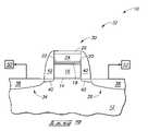
- a TiSi a -comprising layer 24has been formed over, and preferably on as shown, MSi z -comprising layer 22 , where “a” is from 1 to 3.0.
- An exemplary preferred thickness rangeis from 100 Angstroms to 5,000 Angstroms, with a 400 Angstroms thick layer of TiSi 2 being a specific preferred example.
- electrically conductive layer 18 , MSi x N y -comprising layer 20 , and MSi z -comprising layer 22have a combined thickness which is less than that of TiSi a -comprising layer 24 , and in certain preferred embodiments less than that of silicon-comprising layer 16 .
- an electrically insulative layer 26has been formed over, and preferably on as shown, TiSi a -comprising layer 24 .
- Exemplary preferred materialsinclude one or both of silicon dioxide and silicon nitride. Not being electrically conductive, layer 26 will not constitute a conductive portion of the line being formed, and is of course optional.
- silicon-comprising layer 16 , electrically conductive layer 18 , MSi x N y -comprising layer 20 , MSi z -comprising layer 22 and TiSi a -comprising layer 24have been patterned into a stack comprising an electrically conductive line 30 .
- gate dielectric layer 14 and insulative layer 26have also been patterned commensurate with the patterning of electrically conductive layers 16 , 18 , 20 , 22 and 24 .
- Any patterning techniqueis contemplated, and whether existing or yet-to-be developed.
- exemplary techniquesinclude photolithographic patterning and etch, and laser patterning.
- An exemplary dry anisotropic etching chemistry for etching TiSi aincludes CF 4 and Cl 2 .
- An exemplary dry anisotropic etching chemistry for etching MSi w , MSi x N y and MSi xcollectively also includes CF 4 and Cl 2 .
- An exemplary dry anisotropic etching chemistry for etching a polysilicon-comprising layerincludes HBr, He and O 2 .
- MSi xhas been previously promoted for use as a titanium silicide agglomeration-barrier and as a C54 phase titanium silicide promoter, for example as disclosed in our U.S. patent application Ser. No. 10/609,282, filed on Jun. 26, 2003, entitled “Methods of Forming Metal Silicide, and Semiconductor Constructions Comprising Metal Silicide”, and naming Yongjun Jeff Hu as an inventor, now U.S. Pat. No. 7,282,443, the disclosure of which is hereby fully incorporated by reference as if included in its entirety herein.
- an additional MSi x N y -comprising layercan further reduce titanium silicide agglomeration relative to underlying silicon-comprising layers in the fabrication of electrically conductive lines, and regardless of amorphous or crystalline phases.
- An electrically conductive layeris ideally interposed between the silicon-comprising layer and the MSi x N y -comprising layer towards precluding nitrogen of the MSi x N y -comprising layer from coming into contact with the silicon which might undesirably form an insulative silicon nitride.
- the inventionalso contemplates a method of reducing titanium silicide agglomeration in the fabrication of titanium silicide over polysilicon transistor gate lines, which comprises interposing a composite of an MSi z -comprising layer over an MSi x N y -comprising layer over an MSi w -comprising layer intermediate the titanium silicide and polysilicon, where “w” and “z”, respectively, are from 1 to 3.0, where “x” is from zero to 3.0, where “y” is from 0.5 to 10, and “M” is at least one of Ta, Hf, Mo, and W.
- the inventionalso contemplates electrically conductive lines, for example as described above, independent of the method of fabrication, and of course independent of the preferred effects described above.
- electrically conductive line 30can be utilized as a wordline or other field effect transistor gate line, and can be fabricated into transistor gate structures at appropriate locations. Specifically and by way of example only, FIG. 9 shows a location where line 30 has been incorporated into a transistor structure 32 . Source/drain regions 34 and 36 have been formed within substrate 12 . Such exemplary source/drain regions are depicted as comprising a deep, heavily-doped portion, 38 and a shallow, lightly-doped, portion 40 .
- Source/drain regions 34 and 36can be formed utilizing conventional methods or yet-to-be developed methods, and the conductivity-enhancing dopant within regions 38 and 40 can comprise either p-type dopant or n-type dopant, by way of example.
- Electrically insulative sidewall spacers 42have been formed along the sidewalls of electrically conductive line 30 .
- Exemplary preferred materialsinclude one or both of silicon nitride and silicon dioxide.
- Transistor device 32can be incorporated into a memory cell. In the depicted exemplary construction, device 32 is incorporated into a DRAM cell. Specifically, source/drain region 34 is electrically connected to a storage device 50 , and the other source/drain region 36 is electrically connected to a bitline 52 .
- Storage device 50can comprise any suitable device, including a capacitor, for example.
- Bitline 52can comprise any suitable construction. Electrically conductive line 30 can be considered to be part of an integrated circuit, for example the DRAM integrated circuitry just described.
- FIG. 10illustrates generally, by way of example, but not by way of limitation, an embodiment of a computer system 400 according to an aspect of the present invention.
- Computer system 400includes a monitor 401 or other communication output device, a keyboard 402 or other communication input device, and a motherboard 404 .
- Motherboard 404can carry a microprocessor 406 or other data processing unit, and at least one memory device 408 .
- Memory device 408can comprise various aspects of the invention described above, including, for example, one or more of the wordlines, bitlines and DRAM unit cells.
- Memory device 408can comprise an array of memory cells, and such array can be coupled with addressing circuitry for accessing individual memory cells in the array. Further, the memory cell array can be coupled to a read circuit for reading data from the memory cells.
- the addressing and read circuitrycan be utilized for conveying information between memory device 408 and processor 406 . Such is illustrated in the block diagram of the motherboard 404 shown in FIG. 11 . In such block diagram, the addressing circuitry is illustrated as 410 and the read circuitry is illustrated as 412 .
- memory device 408can correspond to a memory module.
- SIMMssingle in-line memory modules
- DIMMsdual in-line memory modules
- the memory devicecan be incorporated into any of a variety of designs which provide different methods of reading from and writing to memory cells of the device.
- One such methodis the page mode operation.
- Page mode operations in a DRAMare defined by the method of accessing a row of a memory cell arrays and randomly accessing different columns of the array. Data stored at the row and column intersection can be read and output while that column is accessed.
- EDOextended data output
- SRAMSecure Digital Random Access Memory
- FIG. 12illustrates a simplified block diagram of a high-level organization of various embodiments of an exemplary electronic system 700 of the present invention.
- System 700can correspond to, for example, a computer system, a process control system, or any other system that employs a processor and associated memory.
- Electronic system 700has functional elements, including a processor or arithmetic/logic unit (ALU) 702 , a control unit 704 , a memory device unit 706 and an input/output (I/O) device 708 .
- ALUarithmetic/logic unit
- Control unit 704coordinates all operations of processor 702 , memory device 706 and I/O devices 708 by continuously cycling through a set of operations that cause instructions to be fetched from memory device 706 and executed.
- memory device 706includes, but is not limited to, random access memory (RAM) devices, read-only memory (ROM) devices, and peripheral devices such as a floppy disk drive and a compact disk CD-ROM drive.
- RAMrandom access memory
- ROMread-only memory
- peripheral devicessuch as a floppy disk drive and a compact disk CD-ROM drive.
- FIG. 13is a simplified block diagram of a high-level organization of various embodiments of an exemplary electronic system 800 .
- the system 800includes a memory device 802 that has an array of memory cells 804 , address decoder 806 , row access circuitry 808 , column access circuitry 810 , read/write control circuitry 812 for controlling operations, and input/output circuitry 814 .
- Memory device 802further includes power circuitry 816 , and sensors 820 , such as current sensors for determining whether a memory cell is in a low-threshold conducting state or in a high-threshold non-conducting state.
- the illustrated power circuitry 816includes power supply circuitry 880 , circuitry 882 for providing a reference voltage, circuitry 884 for providing the first wordline with pulses, circuitry 886 for providing the second wordline with pulses, and circuitry 888 for providing the bitline with pulses.
- System 800also includes a processor 822 , or memory controller for memory accessing.
- Memory device 802receives control signals 824 from processor 822 over wiring or metallization lines. Memory device 802 is used to store data which is accessed via I/O lines. It will be appreciated by those skilled in the art that additional circuitry and control signals can be provided, and that memory device 802 has been simplified to help focus on the invention. At least one of processor 822 or memory device 802 can include a DRAM cell of the type described previously in this disclosure.
- Applications for memory cells, wordlines and bitlinescan include electronic systems for use in memory modules, device drivers, power modules, communication modems, processor modules, and application-specific modules, and may include multilayer, multichip modules.
- Such circuitrycan further be a subcomponent of a variety of electronic systems, such as a clock, a television, a cell phone, a personal computer, an automobile, an industrial control system, an aircraft, and others.
Landscapes
- Engineering & Computer Science (AREA)
- Physics & Mathematics (AREA)
- Condensed Matter Physics & Semiconductors (AREA)
- General Physics & Mathematics (AREA)
- Manufacturing & Machinery (AREA)
- Computer Hardware Design (AREA)
- Microelectronics & Electronic Packaging (AREA)
- Power Engineering (AREA)
- Chemical & Material Sciences (AREA)
- Chemical Kinetics & Catalysis (AREA)
- Semiconductor Memories (AREA)
- Electrodes Of Semiconductors (AREA)
Abstract
Description
- This application is a divisional of U.S. patent application Ser. No. 11/074,106, filed on Mar. 7, 2005, entitled “Electrically Conductive Line, Method of Forming an Electrically Conductive Line, and Method of Reducing Titanium Silicide Agglomeration in Fabrication of Titanium Silicide Over Polysilicon Transistor Gate Lines”, naming Qi Pan, Jiutao Li, Yongjun Jeff Hu, and Allen McTeer, as Inventors, the disclosure of which is incorporated herein by reference.
- This invention relates to electrically conductive lines, to methods of forming electrically conductive lines, and to methods of reducing titanium silicide agglomeration in the fabrication of titanium silicide over polysilicon transistor gate lines.
- One common component found in integrated circuits is an electrically conductive line. Such might form part of a device or subcircuit, or interconnect various devices. One common conductive line is a transistor gate of a field effect transistor device. Such are commonly used in memory integrated circuitry, for example dynamic random access memory (DRAM) circuitry. Individual memory cells of DRAM circuitry include a field effect transistor having one source/drain region thereof electrically connected with a storage capacitor, and the other source/drain region electrically connected with a bitline. The conductive transistor gate lines are commonly referred to as wordlines, with individual gate lines constituting a part of several memory cell field effect transistors.
- A common wordline construction includes titanium silicide (TiSix) received over conductively doped polysilicon. The titanium silicide might be provided over the polysilicon in a number of manners. For example, elemental titanium might be deposited upon polysilicon and thereafter annealed to react the polysilicon and titanium to form titanium silicide. Alternately by way of examples only, titanium silicide might be chemical vapor deposited upon polysilicon or physical vapor deposited by sputtering from a titanium silicide target. Further and regardless, the titanium silicide which is formed might initially be amorphous or crystalline. Crystallinity is desired for reduced resistance/higher conductance. Amorphous titanium silicide can be converted to crystalline titanium suicide by high temperature anneal.
- Crystalline stoichiometric titanium silicide (TiSi2) typically exists in one of two different crystalline phases. A first phase is an orthorhombic base-centered phase having twelve atoms per unit cell, a resistivity of about 60 to 90 microohm-cm, and is known as the C49 phase. A second phase is a more thermodynamically-favored orthorhombic face-centered phase, which has 24 atoms per unit cell and a resistivity of about 12 to 20 microohm-cm, and is known as the C54 phase. Regardless of deposition method, it is common for the less-desired C49 phase to be initially deposited or formed. This C49 phase can then be converted to a desired C54 phase through appropriate annealing conditions.
- One problem associated with the fabrication of such lines is known as agglomeration of the titanium silicide relative to the underlying polysilicon. Such typically manifests when the substrate is exposed to temperatures in excess of 900° C. and which typically inherently occurs during the fabrication of the circuitry. Agglomeration is characterized by the titanium silicide migrating/extending into the underlying polysilicon. Such can be to such a degree to extend completely through the polysilicon. For transistor gate lines, the migration can even be to completely through the gate dielectric, thereby causing a fatal short. Further, the degree of agglomeration is not predictable or controllable from device to device. For transistor gates that are not fatally shorted, this undesirably creates different operating characteristics for different devices. Specifically, the degree of agglomeration within the polysilicon affects its work function and, accordingly, the threshold voltage along the gate line at which individual transistors are turned “on” and “off”.
- In an effort to reduce titanium silicide agglomeration, previous studies have focused on applying different annealing processes or adding other elements to the titanium silicide. Still, needs remain for improved methods of reducing titanium silicide agglomeration in the fabrication of titanium silicide over polysilicon transistor gate lines, and particularly in the fabrication of DRAM circuitry. Yet while the invention was motivated in addressing these issues, it is in no way so limited. The invention is only limited by the accompanying claims as literally worded, without interpretative or other limiting reference to the specification, and in accordance with the doctrine of equivalents.
- The invention includes an electrically conductive line, methods of forming electrically conductive lines, and methods of reducing titanium suicide agglomeration in the fabrication of titanium silicide over polysilicon transistor gate lines. In one implementation, a method of forming an electrically conductive line includes providing a silicon-comprising layer over a substrate. An electrically conductive layer is formed over the silicon-comprising layer. An MSixNy-comprising layer is formed over the electrically conductive layer, where “x” is from 0 to 3.0, “y” is from 0.5 to 10, and “M” is at least one of Ta, Hf, Mo, and W. An MSiz-comprising layer is formed over the MSixNy-comprising layer, where “z” is from 1 to 3.0. A TiSia-comprising layer is formed over the MSiz-comprising layer, where “a” is from 1 to 3.0. The silicon-comprising layer, the electrically conductive layer, the MSixNy-comprising layer, the MSiz-comprising layer, and the TiSia-comprising layer are patterned into a stack comprising an electrically conductive line.
- In one implementation, the invention contemplates an electrically conductive line independent of the method of fabrication.
- In one implementation, a method of reducing titanium suicide agglomeration in fabrication of titanium silicide over polysilicon transistor gate lines comprises interposing a composite of an MSiz-comprising layer over an MSixNy-comprising layer over an MSiw-comprising layer intermediate the titanium silicide and polysilicon, where “w” and “z” respectively are from 1 to 3.0, where “x” is from 0 to 3.0, “y” is from 0.5 to 10, and “M” is at least one of Ta, Hf, Mo, and W.
- Other aspects and implementations are contemplated.
- Preferred embodiments of the invention are described below with reference to the following accompanying drawings.
FIG. 1 is a diagrammatic, cross-sectional view of a semiconductor wafer fragment in process in accordance with an aspect of the invention.FIG. 2 is a view of theFIG. 1 wafer fragment at a point of processing subsequent to that depicted byFIG. 1 .FIG. 3 is a view of theFIG. 2 wafer fragment at a point of processing subsequent to that depicted byFIG. 2 .FIG. 4 is a view of theFIG. 3 wafer fragment at a point of processing subsequent to that depicted byFIG. 3 .FIG. 5 is a view of theFIG. 4 wafer fragment at a point of processing subsequent to that depicted byFIG. 4 .FIG. 6 is a view of theFIG. 5 wafer fragment at a point of processing subsequent to that depicted byFIG. 5 .FIG. 7 is a view of theFIG. 6 wafer fragment at a point of processing subsequent to that depicted byFIG. 6 .FIG. 8 is a view of theFIG. 7 wafer fragment at a point of processing subsequent to that depicted byFIG. 7 .FIG. 9 is a view of theFIG. 8 wafer fragment at a point of processing subsequent to that depicted byFIG. 8 .FIG. 10 is a diagrammatic view of a computer illustrating an exemplary application of the present invention.FIG. 11 is a block diagram showing particular features of the motherboard of theFIG. 10 computer.FIG. 12 is a high-level block diagram of an electronic system according to an exemplary aspect of the present invention.FIG. 13 is a simplified block diagram of an exemplary electronic system according to an aspect of the present invention.- This disclosure of the invention is submitted in furtherance of the constitutional purposes of the U.S. Patent Laws “to promote the progress of science and useful arts” (Article 1, Section 8).
- A preferred method of forming an electrically conductive line, and particularly a field effect transistor gate line, is initially described with reference to
FIGS. 1-9 . Referring toFIG. 1 , a substrate fragment is indicated generally with thereference numeral 10. Such preferably comprises a semiconductor substrate, for example a substrate comprising a bulkmonocrystalline silicon region 12 having agate dielectric layer 14 formed thereover. In the context of this document, the term “semiconductor substrate” or “semiconductive substrate” is defined to mean any construction comprising semiconductive material, including, but not limited to, bulk semiconductive materials such as a semiconductive wafer (either alone or in assemblies comprising other materials thereon), and semiconductive material layers (either alone or in assemblies comprising other materials). The term “substrate” refers to any supporting structure, including, but not limited to, the semiconductive substrates described above. Accordingly,substrate fragment 10 might comprise semiconductor-on-insulator substrates or other substrates, and whether existing or yet-to-be developed. Discussion proceeds with an exemplary preferred fabrication of a transistor gate line with agate dielectric layer 14 thereby being provided. Of course, electrically conductive lines other than field effect transistor gates are also contemplated. An exemplarypreferred material 14 is silicon dioxide deposited or grown to an exemplary thickness of from 10 Angstroms to 100 Angstroms. - Referring to
FIG. 2 , a silicon-comprisinglayer 16 has been formed oversubstrate 12/14. An exemplary preferred silicon-comprisingmaterial 16 is polysilicon. By way of example only, alternate silicon-comprising materials include monocrystalline silicon, such as epitaxially grown silicon, and silicon combined with other materials in a non-compound or non-stoichiometric manner, for example silicon and germanium. Silicon-comprisinglayer 16 will ultimately form a conductive portion of the conductive line, and will thereby at some point be electrically conductive. Accordingly, silicon-comprisinglayer 16 might be electrically conductive as-deposited, for example by in situ doping with a conductivity enhancing impurity during deposition. Alternately, such might be implanted or otherwise processed later to render such layer electrically conductive if not in such state as initially deposited. An exemplary preferred thickness range for silicon-comprisinglayer 16 is from 400 Angstroms to 5,000 Angstroms, with 700 Angstroms being a specific preferred example. - Referring to
FIG. 3 , an electricallyconductive layer 18 has been formed over silicon-comprisinglayer 16. Further preferably and as shown,layer 18 is formed “on” silicon-comprisinglayer 16, with “on” in the context of this document meaning in at least some direct physical contacting relationship with the stated layer. By way of example only, an exemplary preferred material is MSiw, where “w” is from 1 to 3.0 and “M” is at least one of Ta, Hf, Mo, and W. In one preferred embodiment,conductive layer 18 is preferably void of detectable nitrogen to preclude risk of forming an insulative silicon nitride. An exemplary preferred thickness range for electricallyconductive layer 18 is from 5 Angstroms to 500 Angstroms, with from 5 Angstroms to 50 Angstroms being more preferred, and a 50 Angstroms MSi2layer (i.e., even more specifically TaSi2) being a specific preferred example. Such might be deposited by any suitable method, including by way of example only sputtering, chemical vapor deposition and atomic layer deposition. If chemical vapor depositing or atomic layer depositing, exemplary precursors/gasses include SiH4and TaCl4. - Referring to
FIG. 4 , an MSixNy-comprisinglayer 20 has been formed over, and preferably on as shown, electricallyconductive layer 18, and where “x” is from 0 (zero) to 3.0, “y” is from 0.5 to 10, and “M” is at least one of Ta, Hf, Mo, and W. Preferably, “x” is greater than zero, and even more preferably “x” is at least 1. An exemplary preferred thickness range for MSixNy-comprisinglayer 20 is from 10 Angstroms to 500 Angstroms, with from 10 Angstroms to 50 Angstroms being more preferred. A specific example is a 40 Angstroms thick MSixNy-comprising layer where “x” equals 2 and “y” equals 5. MSixNy-comprising layer might be deposited by any existing or yet-to-be developed method, for example including by sputtering, by chemical vapor deposition and by atomic layer deposition. A preferred exemplary sputtering technique comprises a gas sputtered against a target comprising MSiw, with nitrogen being provided at least in part from gaseous N2and/or NH3. For example in one specific preferred embodiment, an inert gas and N2are injected (together or separately) into a sputtering chamber in which the substrate is received at a ratio of inert gas to N2of about 3:1 by volume. - Referring to
FIG. 5 , an MSiz-comprisinglayer 22 is formed over, and preferably on as shown, MSixNy-comprisinglayer 20, and where “z” is from 1 to 3.0 and “M” is at least one of Ta, Hf, Mo, and W. MSiz-comprisinglayer 22 and electricallyconductive layer 18 might be of the same composition (meaning of the same components and in their respective quantities), or of different compositions (meaning of one or both of different components or quantities of the same components). An exemplary preferred thickness range for MSiz-comprisinglayer 22 is from 5 Angstroms to 500 Angstroms, more preferably from 5 Angstroms to 50 Angstroms, with a 60 Angstroms thick MSi2layer being a specific preferred example. - Referring to
FIG. 6 , a TiSia-comprisinglayer 24 has been formed over, and preferably on as shown, MSiz-comprisinglayer 22, where “a” is from 1 to 3.0. An exemplary preferred thickness range is from 100 Angstroms to 5,000 Angstroms, with a 400 Angstroms thick layer of TiSi2being a specific preferred example. In specific preferred examples, electricallyconductive layer 18, MSixNy-comprisinglayer 20, and MSiz-comprisinglayer 22 have a combined thickness which is less than that of TiSia-comprisinglayer 24, and in certain preferred embodiments less than that of silicon-comprisinglayer 16. - Referring to
FIG. 7 , an electricallyinsulative layer 26 has been formed over, and preferably on as shown, TiSia-comprisinglayer 24. Exemplary preferred materials include one or both of silicon dioxide and silicon nitride. Not being electrically conductive,layer 26 will not constitute a conductive portion of the line being formed, and is of course optional. - Referring to
FIG. 8 , silicon-comprisinglayer 16, electricallyconductive layer 18, MSixNy-comprisinglayer 20, MSiz-comprisinglayer 22 and TiSia-comprisinglayer 24 have been patterned into a stack comprising an electricallyconductive line 30. In the depicted exemplary preferredFIG. 8 embodiment,gate dielectric layer 14 andinsulative layer 26 have also been patterned commensurate with the patterning of electricallyconductive layers - MSixhas been previously promoted for use as a titanium silicide agglomeration-barrier and as a C54 phase titanium silicide promoter, for example as disclosed in our U.S. patent application Ser. No. 10/609,282, filed on Jun. 26, 2003, entitled “Methods of Forming Metal Silicide, and Semiconductor Constructions Comprising Metal Silicide”, and naming Yongjun Jeff Hu as an inventor, now U.S. Pat. No. 7,282,443, the disclosure of which is hereby fully incorporated by reference as if included in its entirety herein. Without being limited by any theory or effect unless literally appearing in a claim in this application, the provision of an additional MSixNy-comprising layer can further reduce titanium silicide agglomeration relative to underlying silicon-comprising layers in the fabrication of electrically conductive lines, and regardless of amorphous or crystalline phases. An electrically conductive layer is ideally interposed between the silicon-comprising layer and the MSixNy-comprising layer towards precluding nitrogen of the MSixNy-comprising layer from coming into contact with the silicon which might undesirably form an insulative silicon nitride. Further using the above described etching chemistries, it was found that a conductive line stack in accordance with an aspect of the invention having MSi2over MSi2Nyover MSi2exhibited less undercut than a line stack having MSi2which was void of MSi2Ny.
- In one aspect, the invention also contemplates a method of reducing titanium silicide agglomeration in the fabrication of titanium silicide over polysilicon transistor gate lines, which comprises interposing a composite of an MSiz-comprising layer over an MSixNy-comprising layer over an MSiw-comprising layer intermediate the titanium silicide and polysilicon, where “w” and “z”, respectively, are from 1 to 3.0, where “x” is from zero to 3.0, where “y” is from 0.5 to 10, and “M” is at least one of Ta, Hf, Mo, and W.
- The invention also contemplates electrically conductive lines, for example as described above, independent of the method of fabrication, and of course independent of the preferred effects described above.
- Referring to
FIG. 9 , electricallyconductive line 30 can be utilized as a wordline or other field effect transistor gate line, and can be fabricated into transistor gate structures at appropriate locations. Specifically and by way of example only,FIG. 9 shows a location whereline 30 has been incorporated into atransistor structure 32. Source/drain regions substrate 12. Such exemplary source/drain regions are depicted as comprising a deep, heavily-doped portion,38 and a shallow, lightly-doped,portion 40. Source/drain regions regions insulative sidewall spacers 42 have been formed along the sidewalls of electricallyconductive line 30. Exemplary preferred materials include one or both of silicon nitride and silicon dioxide. Transistor device 32 can be incorporated into a memory cell. In the depicted exemplary construction,device 32 is incorporated into a DRAM cell. Specifically, source/drain region 34 is electrically connected to astorage device 50, and the other source/drain region 36 is electrically connected to abitline 52.Storage device 50 can comprise any suitable device, including a capacitor, for example.Bitline 52 can comprise any suitable construction. Electricallyconductive line 30 can be considered to be part of an integrated circuit, for example the DRAM integrated circuitry just described.FIG. 10 illustrates generally, by way of example, but not by way of limitation, an embodiment of acomputer system 400 according to an aspect of the present invention.Computer system 400 includes amonitor 401 or other communication output device, akeyboard 402 or other communication input device, and amotherboard 404.Motherboard 404 can carry amicroprocessor 406 or other data processing unit, and at least onememory device 408.Memory device 408 can comprise various aspects of the invention described above, including, for example, one or more of the wordlines, bitlines and DRAM unit cells.Memory device 408 can comprise an array of memory cells, and such array can be coupled with addressing circuitry for accessing individual memory cells in the array. Further, the memory cell array can be coupled to a read circuit for reading data from the memory cells. The addressing and read circuitry can be utilized for conveying information betweenmemory device 408 andprocessor 406. Such is illustrated in the block diagram of themotherboard 404 shown inFIG. 11 . In such block diagram, the addressing circuitry is illustrated as410 and the read circuitry is illustrated as412.- In particular aspects of the invention,
memory device 408 can correspond to a memory module. For example, single in-line memory modules (SIMMs) and dual in-line memory modules (DIMMs) may be used in the implementation which utilizes the teachings of the present invention. The memory device can be incorporated into any of a variety of designs which provide different methods of reading from and writing to memory cells of the device. One such method is the page mode operation. Page mode operations in a DRAM are defined by the method of accessing a row of a memory cell arrays and randomly accessing different columns of the array. Data stored at the row and column intersection can be read and output while that column is accessed. - An alternate type of device is the extended data output (EDO) memory which allows data stored at a memory array address to be available as output after the addressed column has been closed. This memory can increase some communication speeds by allowing shorter access signals without reducing the time in which memory output data is available on a memory bus. Other alternative types of devices, by way of example only, include SDRAM, DDR SDRAM, SLDRAM, VRAM and Direct RDRAM, as well as others such as SRAM or Flash memories.
FIG. 12 illustrates a simplified block diagram of a high-level organization of various embodiments of an exemplaryelectronic system 700 of the present invention.System 700 can correspond to, for example, a computer system, a process control system, or any other system that employs a processor and associated memory.Electronic system 700 has functional elements, including a processor or arithmetic/logic unit (ALU)702, acontrol unit 704, amemory device unit 706 and an input/output (I/O)device 708. Generally,electronic system 700 will have a native set of instructions that specify operations to be performed on data byprocessor 702 and other interactions betweenprocessor 702,memory device unit 706 and I/O devices 708.Control unit 704 coordinates all operations ofprocessor 702,memory device 706 and I/O devices 708 by continuously cycling through a set of operations that cause instructions to be fetched frommemory device 706 and executed. In various embodiments,memory device 706 includes, but is not limited to, random access memory (RAM) devices, read-only memory (ROM) devices, and peripheral devices such as a floppy disk drive and a compact disk CD-ROM drive. One of ordinary skill in the art will understand, upon reading and comprehending this disclosure, that any of the illustrated electrical components are capable of being fabricated to include DRAM cells, wordlines and bitlines in accordance with various aspects of the present invention.FIG. 13 is a simplified block diagram of a high-level organization of various embodiments of an exemplaryelectronic system 800. Thesystem 800 includes amemory device 802 that has an array ofmemory cells 804,address decoder 806,row access circuitry 808,column access circuitry 810, read/writecontrol circuitry 812 for controlling operations, and input/output circuitry 814.Memory device 802 further includespower circuitry 816, andsensors 820, such as current sensors for determining whether a memory cell is in a low-threshold conducting state or in a high-threshold non-conducting state. The illustratedpower circuitry 816 includespower supply circuitry 880,circuitry 882 for providing a reference voltage,circuitry 884 for providing the first wordline with pulses,circuitry 886 for providing the second wordline with pulses, andcircuitry 888 for providing the bitline with pulses.System 800 also includes aprocessor 822, or memory controller for memory accessing.Memory device 802 receives control signals824 fromprocessor 822 over wiring or metallization lines.Memory device 802 is used to store data which is accessed via I/O lines. It will be appreciated by those skilled in the art that additional circuitry and control signals can be provided, and thatmemory device 802 has been simplified to help focus on the invention. At least one ofprocessor 822 ormemory device 802 can include a DRAM cell of the type described previously in this disclosure.- The various illustrated systems of this disclosure are intended to provide a general understanding of various applications for the circuitry and structures of the present invention, and are not intended to serve as a complete description of all the elements and features of an electronic system using memory cells in accordance with aspects of the present invention. One of ordinary skill in the art will understand that the various electronic systems can be fabricated in single-package processing units, or even on a single semiconductor chip, in order to reduce the communication time between the processor and the memory device(s).
- Applications for memory cells, wordlines and bitlines can include electronic systems for use in memory modules, device drivers, power modules, communication modems, processor modules, and application-specific modules, and may include multilayer, multichip modules. Such circuitry can further be a subcomponent of a variety of electronic systems, such as a clock, a television, a cell phone, a personal computer, an automobile, an industrial control system, an aircraft, and others.
- In compliance with the statute, the invention has been described in language more or less specific as to structural and methodical features. It is to be understood, however, that the invention is not limited to the specific features shown and described, since the means herein disclosed comprise preferred forms of putting the invention into effect. The invention is, therefore, claimed in any of its forms or modifications within the proper scope of the appended claims appropriately interpreted in accordance with the doctrine of equivalents.
Claims (29)
Priority Applications (1)
| Application Number | Priority Date | Filing Date | Title |
|---|---|---|---|
| US12/173,483US20080284025A1 (en) | 2005-03-07 | 2008-07-15 | Electrically Conductive Line |
Applications Claiming Priority (2)
| Application Number | Priority Date | Filing Date | Title |
|---|---|---|---|
| US11/074,106US7510966B2 (en) | 2005-03-07 | 2005-03-07 | Electrically conductive line, method of forming an electrically conductive line, and method of reducing titanium silicide agglomeration in fabrication of titanium silicide over polysilicon transistor gate lines |
| US12/173,483US20080284025A1 (en) | 2005-03-07 | 2008-07-15 | Electrically Conductive Line |
Related Parent Applications (1)
| Application Number | Title | Priority Date | Filing Date |
|---|---|---|---|
| US11/074,106DivisionUS7510966B2 (en) | 2005-03-07 | 2005-03-07 | Electrically conductive line, method of forming an electrically conductive line, and method of reducing titanium silicide agglomeration in fabrication of titanium silicide over polysilicon transistor gate lines |
Publications (1)
| Publication Number | Publication Date |
|---|---|
| US20080284025A1true US20080284025A1 (en) | 2008-11-20 |
Family
ID=36943362
Family Applications (2)
| Application Number | Title | Priority Date | Filing Date |
|---|---|---|---|
| US11/074,106Active2026-06-04US7510966B2 (en) | 2005-03-07 | 2005-03-07 | Electrically conductive line, method of forming an electrically conductive line, and method of reducing titanium silicide agglomeration in fabrication of titanium silicide over polysilicon transistor gate lines |
| US12/173,483AbandonedUS20080284025A1 (en) | 2005-03-07 | 2008-07-15 | Electrically Conductive Line |
Family Applications Before (1)
| Application Number | Title | Priority Date | Filing Date |
|---|---|---|---|
| US11/074,106Active2026-06-04US7510966B2 (en) | 2005-03-07 | 2005-03-07 | Electrically conductive line, method of forming an electrically conductive line, and method of reducing titanium silicide agglomeration in fabrication of titanium silicide over polysilicon transistor gate lines |
Country Status (1)
| Country | Link |
|---|---|
| US (2) | US7510966B2 (en) |
Families Citing this family (4)
| Publication number | Priority date | Publication date | Assignee | Title |
|---|---|---|---|---|
| GB0506896D0 (en)* | 2005-04-05 | 2005-05-11 | Plastic Logic Ltd | Stack ablation |
| DE102007045074B4 (en)* | 2006-12-27 | 2009-06-18 | Hynix Semiconductor Inc., Ichon | Semiconductor device with gate stack structure |
| US8836048B2 (en) | 2012-10-17 | 2014-09-16 | International Business Machines Corporation | Field effect transistor device having a hybrid metal gate stack |
| US9401279B2 (en) | 2013-06-14 | 2016-07-26 | Sandisk Technologies Llc | Transistor gate and process for making transistor gate |
Citations (95)
| Publication number | Priority date | Publication date | Assignee | Title |
|---|---|---|---|---|
| US3614547A (en)* | 1970-03-16 | 1971-10-19 | Gen Electric | Tungsten barrier electrical connection |
| US3809574A (en)* | 1971-07-15 | 1974-05-07 | Rca Corp | Aluminum oxide films for electronic devices |
| US3990927A (en)* | 1973-11-23 | 1976-11-09 | Commissariat A L'energie Atomique | Method for isolating the components of an integrated circuit |
| US4285761A (en)* | 1980-06-30 | 1981-08-25 | International Business Machines Corporation | Process for selectively forming refractory metal silicide layers on semiconductor devices |
| US4398335A (en)* | 1980-12-09 | 1983-08-16 | Fairchild Camera & Instrument Corporation | Multilayer metal silicide interconnections for integrated circuits |
| US4474975A (en)* | 1983-05-09 | 1984-10-02 | The United States Of America As Represented By The Administrator Of The National Aeronautics And Space Administration | Process for producing tris (N-methylamino) methylsilane |
| US4707723A (en)* | 1985-03-08 | 1987-11-17 | Mitsubishi Denki Kabushiki Kaisha | Semiconductor device using a refractory metal as an electrode and interconnection |
| US4836885A (en)* | 1988-05-03 | 1989-06-06 | International Business Machines Corporation | Planarization process for wide trench isolation |
| US5049975A (en)* | 1989-03-14 | 1991-09-17 | Mitsubishi Denki Kabushiki Kaisha | Multi-layered interconnection structure for a semiconductor device |
| US5105253A (en)* | 1988-12-28 | 1992-04-14 | Synergy Semiconductor Corporation | Structure for a substrate tap in a bipolar structure |
| US5156881A (en)* | 1987-03-18 | 1992-10-20 | Kabushiki Kaisha Toshiba | Method for forming a film on a substrate by activating a reactive gas |
| US5182221A (en)* | 1990-06-13 | 1993-01-26 | Sony Corporation | Method of filling a recess flat with a material by a bias ECR-CVD process |
| US5387539A (en)* | 1992-06-18 | 1995-02-07 | Hyundai Electronics Industries Co., Ltd. | Method of manufacturing trench isolation |
| US5410176A (en)* | 1991-04-05 | 1995-04-25 | Sgs-Thomson Microelectronics, Inc. | Integrated circuit with planarized shallow trench isolation |
| US5444302A (en)* | 1992-12-25 | 1995-08-22 | Hitachi, Ltd. | Semiconductor device including multi-layer conductive thin film of polycrystalline material |
| US5470798A (en)* | 1990-05-29 | 1995-11-28 | Mitel Corporation | Moisture-free sog process |
| US5516721A (en)* | 1993-12-23 | 1996-05-14 | International Business Machines Corporation | Isolation structure using liquid phase oxide deposition |
| US5518959A (en)* | 1995-08-24 | 1996-05-21 | Taiwan Semiconductor Manufacturing Company | Method for selectively depositing silicon oxide spacer layers |
| US5523626A (en)* | 1993-09-08 | 1996-06-04 | Nec Corporation | Semiconductor device and fabrication process therefor |
| US5565376A (en)* | 1994-07-12 | 1996-10-15 | United Microelectronics Corp. | Device isolation technology by liquid phase deposition |
| US5604149A (en)* | 1994-03-11 | 1997-02-18 | France Telecom | Method of and device for isolating active areas of a semiconducor substrate by quasi-plane shallow trenches |
| US5616513A (en)* | 1995-06-01 | 1997-04-01 | International Business Machines Corporation | Shallow trench isolation with self aligned PSG layer |
| US5665629A (en)* | 1995-08-11 | 1997-09-09 | International Business Machines Corporation | Four transistor SRAM process |
| US5719085A (en)* | 1995-09-29 | 1998-02-17 | Intel Corporation | Shallow trench isolation technique |
| US5741740A (en)* | 1997-06-12 | 1998-04-21 | Taiwan Semiconductor Manufacturing Company, Ltd. | Shallow trench isolation (STI) method employing gap filling silicon oxide dielectric layer |
| US5770469A (en)* | 1995-12-29 | 1998-06-23 | Lam Research Corporation | Method for forming semiconductor structure using modulation doped silicate glasses |
| US5786039A (en)* | 1995-05-15 | 1998-07-28 | France Telecom | Process for electrical insulation in microelectronics, applicable in narrow cavities, by deposition of oxide in the viscous state and corresponding device |
| US5786263A (en)* | 1995-04-04 | 1998-07-28 | Motorola, Inc. | Method for forming a trench isolation structure in an integrated circuit |
| US5801083A (en)* | 1997-10-20 | 1998-09-01 | Chartered Semiconductor Manufacturing, Ltd. | Use of polymer spacers for the fabrication of shallow trench isolation regions with rounded top corners |
| US5863827A (en)* | 1997-06-03 | 1999-01-26 | Texas Instruments Incorporated | Oxide deglaze before sidewall oxidation of mesa or trench |
| US5874353A (en)* | 1997-07-31 | 1999-02-23 | United Microelectronics Corporation | Method of forming a self-aligned silicide device |
| US5883006A (en)* | 1997-12-12 | 1999-03-16 | Kabushiki Kaisha Toshiba | Method for making a semiconductor device using a flowable oxide film |
| US5888880A (en)* | 1996-10-30 | 1999-03-30 | Advanced Micro Devices, Inc. | Trench transistor with localized source/drain regions implanted through selectively grown oxide layer |
| US5895253A (en)* | 1997-08-22 | 1999-04-20 | Micron Technology, Inc. | Trench isolation for CMOS devices |
| US5895255A (en)* | 1994-11-30 | 1999-04-20 | Kabushiki Kaisha Toshiba | Shallow trench isolation formation with deep trench cap |
| US5904540A (en)* | 1997-10-18 | 1999-05-18 | United Microelectronics, Corp. | Method for manufacturing shallow trench isolation |
| US5923073A (en)* | 1991-07-01 | 1999-07-13 | Kabushiki Kaisha Toshiba | Method of manufacturing a semiconductor device and semiconductor device manufactured according to the method |
| US5930645A (en)* | 1997-12-18 | 1999-07-27 | Advanced Micro Devices, Inc. | Shallow trench isolation formation with reduced polish stop thickness |
| US5930646A (en)* | 1998-10-09 | 1999-07-27 | Chartered Semiconductor Manufacturing, Ltd. | Method of shallow trench isolation |
| US5943585A (en)* | 1997-12-19 | 1999-08-24 | Advanced Micro Devices, Inc. | Trench isolation structure having low K dielectric spacers arranged upon an oxide liner incorporated with nitrogen |
| US5950094A (en)* | 1999-02-18 | 1999-09-07 | Taiwan Semiconductor Manufacturing Company, Ltd. | Method for fabricating fully dielectric isolated silicon (FDIS) |
| US5960299A (en)* | 1998-10-28 | 1999-09-28 | United Microelectronics Corp. | Method of fabricating a shallow-trench isolation structure in integrated circuit |
| US5972773A (en)* | 1995-03-23 | 1999-10-26 | Advanced Micro Devices, Inc. | High quality isolation for high density and high performance integrated circuits |
| US6013583A (en)* | 1996-06-25 | 2000-01-11 | International Business Machines Corporation | Low temperature BPSG deposition process |
| US6030881A (en)* | 1998-05-05 | 2000-02-29 | Novellus Systems, Inc. | High throughput chemical vapor deposition process capable of filling high aspect ratio structures |
| US6033961A (en)* | 1998-04-30 | 2000-03-07 | Hewlett-Packard Company | Isolation trench fabrication process |
| US6051477A (en)* | 1995-11-01 | 2000-04-18 | Hyundai Electronics Industries Co., Ltd. | Method of fabricating semiconductor device |
| US6069055A (en)* | 1996-07-12 | 2000-05-30 | Matsushita Electric Industrial Co., Ltd. | Fabricating method for semiconductor device |
| US6090675A (en)* | 1999-04-02 | 2000-07-18 | Taiwan Semiconductor Manufacturing Company | Formation of dielectric layer employing high ozone:tetraethyl-ortho-silicate ratios during chemical vapor deposition |
| US6103607A (en)* | 1998-09-15 | 2000-08-15 | Lucent Technologies | Manufacture of MOSFET devices |
| US6127737A (en)* | 1997-04-11 | 2000-10-03 | Mitsubishi Denki Kabushiki Kaisha | Semiconductor device and manufacturing method thereof |
| US6171962B1 (en)* | 1997-12-18 | 2001-01-09 | Advanced Micro Devices, Inc. | Shallow trench isolation formation without planarization mask |
| US6187651B1 (en)* | 1998-05-07 | 2001-02-13 | Samsung Electronics Co., Ltd. | Methods of forming trench isolation regions using preferred stress relieving layers and techniques to inhibit the occurrence of voids |
| US6191002B1 (en)* | 1998-04-27 | 2001-02-20 | Nec Corporation | Method of forming trench isolation structure |
| US6190979B1 (en)* | 1999-07-12 | 2001-02-20 | International Business Machines Corporation | Method for fabricating dual workfunction devices on a semiconductor substrate using counter-doping and gapfill |
| US6245641B1 (en)* | 1998-01-30 | 2001-06-12 | Mitsubishi Denki Kabushiki Kaisha | Semiconductor device comprising trench isolation insulator film and method of fabricating the same |
| US6255187B1 (en)* | 1999-04-21 | 2001-07-03 | Samsung Electronics Co., Ltd. | Method of fabricating self-aligning stacked capacitor using electroplating method |
| US20010006839A1 (en)* | 1999-12-30 | 2001-07-05 | In-Seok Yeo | Method for manufacturing shallow trench isolation in semiconductor device |
| US20010006255A1 (en)* | 1998-06-24 | 2001-07-05 | Kwon Dong-Chul | Semiconductor device having improved metal line structure and manufacturing method therefor |
| US6265282B1 (en)* | 1998-08-17 | 2001-07-24 | Micron Technology, Inc. | Process for making an isolation structure |
| US6271590B1 (en)* | 1998-08-21 | 2001-08-07 | Micron Technology, Inc. | Graded layer for use in semiconductor circuits and method for making same |
| US6300219B1 (en)* | 1999-08-30 | 2001-10-09 | Micron Technology, Inc. | Method of forming trench isolation regions |
| US20020000195A1 (en)* | 2000-04-10 | 2002-01-03 | Won Bang | Concentration profile on demand gas delivery system (individual divert delivery system) |
| US20020004284A1 (en)* | 1998-08-25 | 2002-01-10 | Terry Chen | Method for forming a shallow trench isolation structure including a dummy pattern in the wider trench |
| US20020003267A1 (en)* | 1998-07-22 | 2002-01-10 | Lee Eun-Ha | Gate electrode having agglomeration preventing layer on metal silicide layer, and method for forming the same |
| US20020018849A1 (en)* | 2000-06-29 | 2002-02-14 | George Steven M. | Method for forming SIO2 by chemical vapor deposition at room temperature |
| US6355966B1 (en)* | 2000-03-01 | 2002-03-12 | Micron Technology, Inc. | Methods of forming an integrated circuitry isolation trench, method of forming integrated circuitry, and integrated circuitry |
| US20020109199A1 (en)* | 2000-06-22 | 2002-08-15 | Moore John T. | Transistor devices |
| US6448150B1 (en)* | 1998-01-20 | 2002-09-10 | Nanya Technology Corporation | Method for forming shallow trench isolation in the integrated circuit |
| US6455394B1 (en)* | 1998-03-13 | 2002-09-24 | Micron Technology, Inc. | Method for trench isolation by selective deposition of low temperature oxide films |
| US20030032281A1 (en)* | 2000-03-07 | 2003-02-13 | Werkhoven Christiaan J. | Graded thin films |
| US6524912B1 (en)* | 2000-08-31 | 2003-02-25 | Micron Technology, Inc. | Planarization of metal container structures |
| US6583060B2 (en)* | 2001-07-13 | 2003-06-24 | Micron Technology, Inc. | Dual depth trench isolation |
| US6607959B2 (en)* | 2000-11-30 | 2003-08-19 | Samsung Electronics Co., Ltd. | Integrated circuit devices having trench isolation structures and methods of fabricating the same |
| US6617251B1 (en)* | 2001-06-19 | 2003-09-09 | Lsi Logic Corporation | Method of shallow trench isolation formation and planarization |
| US20030207556A1 (en)* | 1998-02-26 | 2003-11-06 | Weimer Ronald A. | Forming a conductive structure in a semiconductor device |
| US6674132B2 (en)* | 2000-08-09 | 2004-01-06 | Infineon Technologies Ag | Memory cell and production method |
| US20040016987A1 (en)* | 2002-07-10 | 2004-01-29 | Mitsubishi Denki Kabushiki Kaisha | Semiconductor device with insulator and manufacturing method therefor |
| US20040032006A1 (en)* | 2002-08-19 | 2004-02-19 | Eun-Jung Yun | Trench structure and method of forming the same |
| US6720604B1 (en)* | 1999-01-13 | 2004-04-13 | Agere Systems Inc. | Capacitor for an integrated circuit |
| US20040129670A1 (en)* | 2002-12-30 | 2004-07-08 | Soon-Yong Kweon | Method for fabricating ferroelectric random access memory device |
| US20040166687A1 (en)* | 2003-02-26 | 2004-08-26 | Yung-Chang Lin | Method for forming a polycide gate and structure of the same |
| US20040209484A1 (en)* | 2003-04-21 | 2004-10-21 | Hill Chris W. | Method of depositing a silicon dioxide comprising layer doped with at least one of P, B and Ge |
| US20050009293A1 (en)* | 2003-07-10 | 2005-01-13 | Samsung Electronics Co., Ltd | Method of forming trench isolations |
| US20050009368A1 (en)* | 2003-07-07 | 2005-01-13 | Vaartstra Brian A. | Methods of forming a phosphorus doped silicon dioxide comprising layer, and methods of forming trench isolation in the fabrication of integrated circuitry |
| US20050020045A1 (en)* | 2001-11-29 | 2005-01-27 | Tetsuya Taguwa | Semiconductor device having a low-resistance gate electrode |
| US20050054213A1 (en)* | 2003-09-05 | 2005-03-10 | Derderian Garo J. | Methods of depositing a silicon dioxide comprising layer in the fabrication of integrated circuitry, and methods of forming trench isolation in the fabrication of integrated circuitry |
| US20050079730A1 (en)* | 2003-10-10 | 2005-04-14 | Infineon Technologies North America Corp. | Trench isolation employing a high aspect ratio trench |
| US20050112282A1 (en)* | 2002-03-28 | 2005-05-26 | President And Fellows Of Harvard College | Vapor deposition of silicon dioxide nanolaminates |
| US20050142799A1 (en)* | 2003-12-31 | 2005-06-30 | Dongbuanam Semiconductor Inc. | Method for forming STI of semiconductor device |
| US7053010B2 (en)* | 2004-03-22 | 2006-05-30 | Micron Technology, Inc. | Methods of depositing silicon dioxide comprising layers in the fabrication of integrated circuitry, methods of forming trench isolation, and methods of forming arrays of memory cells |
| US20070018245A1 (en)* | 2005-07-06 | 2007-01-25 | Applied Intellectual Properties Co., Ltd. | Fringing field induced localized charge trapping memory |
| US7235459B2 (en)* | 2004-08-31 | 2007-06-26 | Micron Technology, Inc. | Methods of forming trench isolation in the fabrication of integrated circuitry, methods of fabricating memory circuitry, integrated circuitry and memory integrated circuitry |
| US7282443B2 (en)* | 2003-06-26 | 2007-10-16 | Micron Technology, Inc. | Methods of forming metal silicide |
| US20090186459A1 (en)* | 2004-07-21 | 2009-07-23 | Powerchip Semiconductor Corp. | Manufacturing method of non-volatile memory |
Family Cites Families (20)
| Publication number | Priority date | Publication date | Assignee | Title |
|---|---|---|---|---|
| JPH02277253A (en) | 1989-04-18 | 1990-11-13 | Mitsubishi Electric Corp | Manufacturing method of semiconductor device |
| US5105888A (en) | 1991-04-10 | 1992-04-21 | Pollock J Roark | Well casing hanger and packoff running and retrieval tool |
| JP3163719B2 (en) | 1992-01-30 | 2001-05-08 | ソニー株式会社 | Method for manufacturing semiconductor device having polishing step |
| JPH06334031A (en) | 1993-05-25 | 1994-12-02 | Nec Corp | Element-isolation method for semiconductor device |
| JPH08146224A (en) | 1994-11-21 | 1996-06-07 | Kyocera Corp | Liquid crystal display |
| US5702977A (en) | 1997-03-03 | 1997-12-30 | Taiwan Semiconductor Manufacturing Company, Ltd. | Shallow trench isolation method employing self-aligned and planarized trench fill dielectric layer |
| TW334614B (en) | 1997-03-04 | 1998-06-21 | Winbond Electronics Corp | The method of forming shallow trench isolation |
| US5981354A (en) | 1997-03-12 | 1999-11-09 | Advanced Micro Devices, Inc. | Semiconductor fabrication employing a flowable oxide to enhance planarization in a shallow trench isolation process |
| US6097076A (en) | 1997-03-25 | 2000-08-01 | Micron Technology, Inc. | Self-aligned isolation trench |
| TWI246633B (en) | 1997-12-12 | 2006-01-01 | Applied Materials Inc | Method of pattern etching a low k dielectric layen |
| US5998280A (en) | 1998-03-20 | 1999-12-07 | National Semiconductor Corporation | Modified recessed locos isolation process for deep sub-micron device processes |
| KR100280106B1 (en) | 1998-04-16 | 2001-03-02 | 윤종용 | How to form trench isolation |
| JP3208376B2 (en) | 1998-05-20 | 2001-09-10 | 株式会社半導体プロセス研究所 | Film forming method and semiconductor device manufacturing method |
| KR100286736B1 (en) | 1998-06-16 | 2001-04-16 | 윤종용 | How to form trench isolation |
| US5989978A (en) | 1998-07-16 | 1999-11-23 | Chartered Semiconductor Manufacturing, Ltd. | Shallow trench isolation of MOSFETS with reduced corner parasitic currents |
| US6156674A (en) | 1998-11-25 | 2000-12-05 | Micron Technology, Inc. | Semiconductor processing methods of forming insulative materials |
| EP1292970B1 (en)* | 2000-06-08 | 2011-09-28 | Genitech Inc. | Thin film forming method |
| KR100815009B1 (en) | 2000-09-28 | 2008-03-18 | 프레지던트 앤드 펠로우즈 오브 하바드 칼리지 | Precipitation Using Vapors of Oxides, Silicates and Phosphates |
| US6853072B2 (en) | 2002-04-17 | 2005-02-08 | Sanyo Electric Co., Ltd. | Semiconductor switching circuit device and manufacturing method thereof |
| US6821865B2 (en) | 2002-12-30 | 2004-11-23 | Infineon Technologies Ag | Deep isolation trenches |
- 2005
- 2005-03-07USUS11/074,106patent/US7510966B2/enactiveActive
- 2008
- 2008-07-15USUS12/173,483patent/US20080284025A1/ennot_activeAbandoned
Patent Citations (106)
| Publication number | Priority date | Publication date | Assignee | Title |
|---|---|---|---|---|
| US3614547A (en)* | 1970-03-16 | 1971-10-19 | Gen Electric | Tungsten barrier electrical connection |
| US3809574A (en)* | 1971-07-15 | 1974-05-07 | Rca Corp | Aluminum oxide films for electronic devices |
| US3990927A (en)* | 1973-11-23 | 1976-11-09 | Commissariat A L'energie Atomique | Method for isolating the components of an integrated circuit |
| US4285761A (en)* | 1980-06-30 | 1981-08-25 | International Business Machines Corporation | Process for selectively forming refractory metal silicide layers on semiconductor devices |
| US4398335A (en)* | 1980-12-09 | 1983-08-16 | Fairchild Camera & Instrument Corporation | Multilayer metal silicide interconnections for integrated circuits |
| US4474975A (en)* | 1983-05-09 | 1984-10-02 | The United States Of America As Represented By The Administrator Of The National Aeronautics And Space Administration | Process for producing tris (N-methylamino) methylsilane |
| US4707723A (en)* | 1985-03-08 | 1987-11-17 | Mitsubishi Denki Kabushiki Kaisha | Semiconductor device using a refractory metal as an electrode and interconnection |
| US5156881A (en)* | 1987-03-18 | 1992-10-20 | Kabushiki Kaisha Toshiba | Method for forming a film on a substrate by activating a reactive gas |
| US5776557A (en)* | 1987-03-18 | 1998-07-07 | Kabushiki Kaisha Toshiba | Method for forming a film on a substrate by activating a reactive gas |
| US4836885A (en)* | 1988-05-03 | 1989-06-06 | International Business Machines Corporation | Planarization process for wide trench isolation |
| US5105253A (en)* | 1988-12-28 | 1992-04-14 | Synergy Semiconductor Corporation | Structure for a substrate tap in a bipolar structure |
| US5049975A (en)* | 1989-03-14 | 1991-09-17 | Mitsubishi Denki Kabushiki Kaisha | Multi-layered interconnection structure for a semiconductor device |
| US5470798A (en)* | 1990-05-29 | 1995-11-28 | Mitel Corporation | Moisture-free sog process |
| US5182221A (en)* | 1990-06-13 | 1993-01-26 | Sony Corporation | Method of filling a recess flat with a material by a bias ECR-CVD process |
| US5410176A (en)* | 1991-04-05 | 1995-04-25 | Sgs-Thomson Microelectronics, Inc. | Integrated circuit with planarized shallow trench isolation |
| US5923073A (en)* | 1991-07-01 | 1999-07-13 | Kabushiki Kaisha Toshiba | Method of manufacturing a semiconductor device and semiconductor device manufactured according to the method |
| US5387539A (en)* | 1992-06-18 | 1995-02-07 | Hyundai Electronics Industries Co., Ltd. | Method of manufacturing trench isolation |
| US5444302A (en)* | 1992-12-25 | 1995-08-22 | Hitachi, Ltd. | Semiconductor device including multi-layer conductive thin film of polycrystalline material |
| US5523626A (en)* | 1993-09-08 | 1996-06-04 | Nec Corporation | Semiconductor device and fabrication process therefor |
| US5516721A (en)* | 1993-12-23 | 1996-05-14 | International Business Machines Corporation | Isolation structure using liquid phase oxide deposition |
| US5604149A (en)* | 1994-03-11 | 1997-02-18 | France Telecom | Method of and device for isolating active areas of a semiconducor substrate by quasi-plane shallow trenches |
| US5565376A (en)* | 1994-07-12 | 1996-10-15 | United Microelectronics Corp. | Device isolation technology by liquid phase deposition |
| US5895255A (en)* | 1994-11-30 | 1999-04-20 | Kabushiki Kaisha Toshiba | Shallow trench isolation formation with deep trench cap |
| US5972773A (en)* | 1995-03-23 | 1999-10-26 | Advanced Micro Devices, Inc. | High quality isolation for high density and high performance integrated circuits |
| US5786263A (en)* | 1995-04-04 | 1998-07-28 | Motorola, Inc. | Method for forming a trench isolation structure in an integrated circuit |
| US5786039A (en)* | 1995-05-15 | 1998-07-28 | France Telecom | Process for electrical insulation in microelectronics, applicable in narrow cavities, by deposition of oxide in the viscous state and corresponding device |
| US5616513A (en)* | 1995-06-01 | 1997-04-01 | International Business Machines Corporation | Shallow trench isolation with self aligned PSG layer |
| US5665629A (en)* | 1995-08-11 | 1997-09-09 | International Business Machines Corporation | Four transistor SRAM process |
| US5518959A (en)* | 1995-08-24 | 1996-05-21 | Taiwan Semiconductor Manufacturing Company | Method for selectively depositing silicon oxide spacer layers |
| US5719085A (en)* | 1995-09-29 | 1998-02-17 | Intel Corporation | Shallow trench isolation technique |
| US6051477A (en)* | 1995-11-01 | 2000-04-18 | Hyundai Electronics Industries Co., Ltd. | Method of fabricating semiconductor device |
| US5770469A (en)* | 1995-12-29 | 1998-06-23 | Lam Research Corporation | Method for forming semiconductor structure using modulation doped silicate glasses |
| US6013583A (en)* | 1996-06-25 | 2000-01-11 | International Business Machines Corporation | Low temperature BPSG deposition process |
| US6069055A (en)* | 1996-07-12 | 2000-05-30 | Matsushita Electric Industrial Co., Ltd. | Fabricating method for semiconductor device |
| US5888880A (en)* | 1996-10-30 | 1999-03-30 | Advanced Micro Devices, Inc. | Trench transistor with localized source/drain regions implanted through selectively grown oxide layer |
| US6127737A (en)* | 1997-04-11 | 2000-10-03 | Mitsubishi Denki Kabushiki Kaisha | Semiconductor device and manufacturing method thereof |
| US5863827A (en)* | 1997-06-03 | 1999-01-26 | Texas Instruments Incorporated | Oxide deglaze before sidewall oxidation of mesa or trench |
| US5741740A (en)* | 1997-06-12 | 1998-04-21 | Taiwan Semiconductor Manufacturing Company, Ltd. | Shallow trench isolation (STI) method employing gap filling silicon oxide dielectric layer |
| US5874353A (en)* | 1997-07-31 | 1999-02-23 | United Microelectronics Corporation | Method of forming a self-aligned silicide device |
| US5895253A (en)* | 1997-08-22 | 1999-04-20 | Micron Technology, Inc. | Trench isolation for CMOS devices |
| US5904540A (en)* | 1997-10-18 | 1999-05-18 | United Microelectronics, Corp. | Method for manufacturing shallow trench isolation |
| US5801083A (en)* | 1997-10-20 | 1998-09-01 | Chartered Semiconductor Manufacturing, Ltd. | Use of polymer spacers for the fabrication of shallow trench isolation regions with rounded top corners |
| US5883006A (en)* | 1997-12-12 | 1999-03-16 | Kabushiki Kaisha Toshiba | Method for making a semiconductor device using a flowable oxide film |
| US6171962B1 (en)* | 1997-12-18 | 2001-01-09 | Advanced Micro Devices, Inc. | Shallow trench isolation formation without planarization mask |
| US5930645A (en)* | 1997-12-18 | 1999-07-27 | Advanced Micro Devices, Inc. | Shallow trench isolation formation with reduced polish stop thickness |
| US5943585A (en)* | 1997-12-19 | 1999-08-24 | Advanced Micro Devices, Inc. | Trench isolation structure having low K dielectric spacers arranged upon an oxide liner incorporated with nitrogen |
| US6448150B1 (en)* | 1998-01-20 | 2002-09-10 | Nanya Technology Corporation | Method for forming shallow trench isolation in the integrated circuit |
| US6245641B1 (en)* | 1998-01-30 | 2001-06-12 | Mitsubishi Denki Kabushiki Kaisha | Semiconductor device comprising trench isolation insulator film and method of fabricating the same |
| US20030207556A1 (en)* | 1998-02-26 | 2003-11-06 | Weimer Ronald A. | Forming a conductive structure in a semiconductor device |
| US6455394B1 (en)* | 1998-03-13 | 2002-09-24 | Micron Technology, Inc. | Method for trench isolation by selective deposition of low temperature oxide films |
| US6191002B1 (en)* | 1998-04-27 | 2001-02-20 | Nec Corporation | Method of forming trench isolation structure |
| US6033961A (en)* | 1998-04-30 | 2000-03-07 | Hewlett-Packard Company | Isolation trench fabrication process |
| US6030881A (en)* | 1998-05-05 | 2000-02-29 | Novellus Systems, Inc. | High throughput chemical vapor deposition process capable of filling high aspect ratio structures |
| US6187651B1 (en)* | 1998-05-07 | 2001-02-13 | Samsung Electronics Co., Ltd. | Methods of forming trench isolation regions using preferred stress relieving layers and techniques to inhibit the occurrence of voids |
| US20010006255A1 (en)* | 1998-06-24 | 2001-07-05 | Kwon Dong-Chul | Semiconductor device having improved metal line structure and manufacturing method therefor |
| US20020003267A1 (en)* | 1998-07-22 | 2002-01-10 | Lee Eun-Ha | Gate electrode having agglomeration preventing layer on metal silicide layer, and method for forming the same |
| US6265282B1 (en)* | 1998-08-17 | 2001-07-24 | Micron Technology, Inc. | Process for making an isolation structure |
| US6271590B1 (en)* | 1998-08-21 | 2001-08-07 | Micron Technology, Inc. | Graded layer for use in semiconductor circuits and method for making same |
| US6545356B2 (en)* | 1998-08-21 | 2003-04-08 | Micron Technology, Inc. | Graded layer for use in semiconductor circuits and method for making same |
| US20020004284A1 (en)* | 1998-08-25 | 2002-01-10 | Terry Chen | Method for forming a shallow trench isolation structure including a dummy pattern in the wider trench |
| US6103607A (en)* | 1998-09-15 | 2000-08-15 | Lucent Technologies | Manufacture of MOSFET devices |
| US5930646A (en)* | 1998-10-09 | 1999-07-27 | Chartered Semiconductor Manufacturing, Ltd. | Method of shallow trench isolation |
| US5960299A (en)* | 1998-10-28 | 1999-09-28 | United Microelectronics Corp. | Method of fabricating a shallow-trench isolation structure in integrated circuit |
| US6720604B1 (en)* | 1999-01-13 | 2004-04-13 | Agere Systems Inc. | Capacitor for an integrated circuit |
| US5950094A (en)* | 1999-02-18 | 1999-09-07 | Taiwan Semiconductor Manufacturing Company, Ltd. | Method for fabricating fully dielectric isolated silicon (FDIS) |
| US6090675A (en)* | 1999-04-02 | 2000-07-18 | Taiwan Semiconductor Manufacturing Company | Formation of dielectric layer employing high ozone:tetraethyl-ortho-silicate ratios during chemical vapor deposition |
| US6255187B1 (en)* | 1999-04-21 | 2001-07-03 | Samsung Electronics Co., Ltd. | Method of fabricating self-aligning stacked capacitor using electroplating method |
| US6190979B1 (en)* | 1999-07-12 | 2001-02-20 | International Business Machines Corporation | Method for fabricating dual workfunction devices on a semiconductor substrate using counter-doping and gapfill |
| US6583028B2 (en)* | 1999-08-30 | 2003-06-24 | Micron Technology, Inc. | Methods of forming trench isolation regions |
| US6300219B1 (en)* | 1999-08-30 | 2001-10-09 | Micron Technology, Inc. | Method of forming trench isolation regions |
| US20040082181A1 (en)* | 1999-08-30 | 2004-04-29 | Doan Trung Tri | Methods of forming trench isolation regions |
| US6719012B2 (en)* | 1999-08-30 | 2004-04-13 | Micron Technology, Inc. | Method of forming trench isolation regions |
| US20010006839A1 (en)* | 1999-12-30 | 2001-07-05 | In-Seok Yeo | Method for manufacturing shallow trench isolation in semiconductor device |
| US6355966B1 (en)* | 2000-03-01 | 2002-03-12 | Micron Technology, Inc. | Methods of forming an integrated circuitry isolation trench, method of forming integrated circuitry, and integrated circuitry |
| US20030032281A1 (en)* | 2000-03-07 | 2003-02-13 | Werkhoven Christiaan J. | Graded thin films |
| US6933225B2 (en)* | 2000-03-07 | 2005-08-23 | Asm International N.V. | Graded thin films |
| US6534395B2 (en)* | 2000-03-07 | 2003-03-18 | Asm Microchemistry Oy | Method of forming graded thin films using alternating pulses of vapor phase reactants |
| US20030129826A1 (en)* | 2000-03-07 | 2003-07-10 | Werkhoven Christiaan J. | Graded thin films |
| US20020000195A1 (en)* | 2000-04-10 | 2002-01-03 | Won Bang | Concentration profile on demand gas delivery system (individual divert delivery system) |
| US20020109199A1 (en)* | 2000-06-22 | 2002-08-15 | Moore John T. | Transistor devices |
| US20020018849A1 (en)* | 2000-06-29 | 2002-02-14 | George Steven M. | Method for forming SIO2 by chemical vapor deposition at room temperature |
| US6674132B2 (en)* | 2000-08-09 | 2004-01-06 | Infineon Technologies Ag | Memory cell and production method |
| US6524912B1 (en)* | 2000-08-31 | 2003-02-25 | Micron Technology, Inc. | Planarization of metal container structures |
| US6607959B2 (en)* | 2000-11-30 | 2003-08-19 | Samsung Electronics Co., Ltd. | Integrated circuit devices having trench isolation structures and methods of fabricating the same |
| US6617251B1 (en)* | 2001-06-19 | 2003-09-09 | Lsi Logic Corporation | Method of shallow trench isolation formation and planarization |
| US6583060B2 (en)* | 2001-07-13 | 2003-06-24 | Micron Technology, Inc. | Dual depth trench isolation |
| US20050020045A1 (en)* | 2001-11-29 | 2005-01-27 | Tetsuya Taguwa | Semiconductor device having a low-resistance gate electrode |
| US20050112282A1 (en)* | 2002-03-28 | 2005-05-26 | President And Fellows Of Harvard College | Vapor deposition of silicon dioxide nanolaminates |
| US20040016987A1 (en)* | 2002-07-10 | 2004-01-29 | Mitsubishi Denki Kabushiki Kaisha | Semiconductor device with insulator and manufacturing method therefor |
| US20040032006A1 (en)* | 2002-08-19 | 2004-02-19 | Eun-Jung Yun | Trench structure and method of forming the same |
| US20040129670A1 (en)* | 2002-12-30 | 2004-07-08 | Soon-Yong Kweon | Method for fabricating ferroelectric random access memory device |
| US20040166687A1 (en)* | 2003-02-26 | 2004-08-26 | Yung-Chang Lin | Method for forming a polycide gate and structure of the same |
| US20040209484A1 (en)* | 2003-04-21 | 2004-10-21 | Hill Chris W. | Method of depositing a silicon dioxide comprising layer doped with at least one of P, B and Ge |
| US6930058B2 (en)* | 2003-04-21 | 2005-08-16 | Micron Technology, Inc. | Method of depositing a silicon dioxide comprising layer doped with at least one of P, B and Ge |
| US7282443B2 (en)* | 2003-06-26 | 2007-10-16 | Micron Technology, Inc. | Methods of forming metal silicide |
| US20050009368A1 (en)* | 2003-07-07 | 2005-01-13 | Vaartstra Brian A. | Methods of forming a phosphorus doped silicon dioxide comprising layer, and methods of forming trench isolation in the fabrication of integrated circuitry |
| US20050124171A1 (en)* | 2003-07-07 | 2005-06-09 | Vaartstra Brian A. | Method of forming trench isolation in the fabrication of integrated circuitry |
| US7033909B2 (en)* | 2003-07-10 | 2006-04-25 | Samsung Electronics Co., Ltd. | Method of forming trench isolations |
| US20050009293A1 (en)* | 2003-07-10 | 2005-01-13 | Samsung Electronics Co., Ltd | Method of forming trench isolations |
| US20050054213A1 (en)* | 2003-09-05 | 2005-03-10 | Derderian Garo J. | Methods of depositing a silicon dioxide comprising layer in the fabrication of integrated circuitry, and methods of forming trench isolation in the fabrication of integrated circuitry |
| US20050079730A1 (en)* | 2003-10-10 | 2005-04-14 | Infineon Technologies North America Corp. | Trench isolation employing a high aspect ratio trench |
| US20050142799A1 (en)* | 2003-12-31 | 2005-06-30 | Dongbuanam Semiconductor Inc. | Method for forming STI of semiconductor device |
| US7053010B2 (en)* | 2004-03-22 | 2006-05-30 | Micron Technology, Inc. | Methods of depositing silicon dioxide comprising layers in the fabrication of integrated circuitry, methods of forming trench isolation, and methods of forming arrays of memory cells |
| US20090186459A1 (en)* | 2004-07-21 | 2009-07-23 | Powerchip Semiconductor Corp. | Manufacturing method of non-volatile memory |
| US7235459B2 (en)* | 2004-08-31 | 2007-06-26 | Micron Technology, Inc. | Methods of forming trench isolation in the fabrication of integrated circuitry, methods of fabricating memory circuitry, integrated circuitry and memory integrated circuitry |
| US20070018245A1 (en)* | 2005-07-06 | 2007-01-25 | Applied Intellectual Properties Co., Ltd. | Fringing field induced localized charge trapping memory |
Also Published As
| Publication number | Publication date |
|---|---|
| US20060197225A1 (en) | 2006-09-07 |
| US7510966B2 (en) | 2009-03-31 |
Similar Documents
| Publication | Publication Date | Title |
|---|---|---|
| US7019351B2 (en) | Transistor devices, and methods of forming transistor devices and circuit devices | |
| US7176073B2 (en) | Methods of forming memory cells having diodes and electrode plates connected to source/drain regions | |
| US6958263B2 (en) | Methods of forming devices, constructions and systems comprising thyristors | |
| US7217630B2 (en) | Methods of forming hafnium oxide | |
| US7687358B2 (en) | Methods of forming a gated device | |
| US7405110B2 (en) | Methods of forming implant regions relative to transistor gates | |
| KR100961067B1 (en) | Method of forming a memory circuit with different insulating sidewall spacers | |
| US7282443B2 (en) | Methods of forming metal silicide | |
| US20080284025A1 (en) | Electrically Conductive Line | |
| US8435889B2 (en) | Methods of forming CoSi2, methods of forming field effect transistors, and methods of forming conductive contacts | |
| US6881636B2 (en) | Methods of forming deuterated silicon nitride-containing materials | |
| US7341951B2 (en) | Methods of forming semiconductor constructions |
Legal Events
| Date | Code | Title | Description |
|---|---|---|---|
| AS | Assignment | Owner name:U.S. BANK NATIONAL ASSOCIATION, AS COLLATERAL AGENT, CALIFORNIA Free format text:SECURITY INTEREST;ASSIGNOR:MICRON TECHNOLOGY, INC.;REEL/FRAME:038669/0001 Effective date:20160426 Owner name:U.S. BANK NATIONAL ASSOCIATION, AS COLLATERAL AGEN Free format text:SECURITY INTEREST;ASSIGNOR:MICRON TECHNOLOGY, INC.;REEL/FRAME:038669/0001 Effective date:20160426 | |
| AS | Assignment | Owner name:MORGAN STANLEY SENIOR FUNDING, INC., AS COLLATERAL AGENT, MARYLAND Free format text:PATENT SECURITY AGREEMENT;ASSIGNOR:MICRON TECHNOLOGY, INC.;REEL/FRAME:038954/0001 Effective date:20160426 Owner name:MORGAN STANLEY SENIOR FUNDING, INC., AS COLLATERAL Free format text:PATENT SECURITY AGREEMENT;ASSIGNOR:MICRON TECHNOLOGY, INC.;REEL/FRAME:038954/0001 Effective date:20160426 | |
| STCB | Information on status: application discontinuation | Free format text:ABANDONED -- FAILURE TO PAY ISSUE FEE | |
| AS | Assignment | Owner name:U.S. BANK NATIONAL ASSOCIATION, AS COLLATERAL AGENT, CALIFORNIA Free format text:CORRECTIVE ASSIGNMENT TO CORRECT THE REPLACE ERRONEOUSLY FILED PATENT #7358718 WITH THE CORRECT PATENT #7358178 PREVIOUSLY RECORDED ON REEL 038669 FRAME 0001. ASSIGNOR(S) HEREBY CONFIRMS THE SECURITY INTEREST;ASSIGNOR:MICRON TECHNOLOGY, INC.;REEL/FRAME:043079/0001 Effective date:20160426 Owner name:U.S. BANK NATIONAL ASSOCIATION, AS COLLATERAL AGEN Free format text:CORRECTIVE ASSIGNMENT TO CORRECT THE REPLACE ERRONEOUSLY FILED PATENT #7358718 WITH THE CORRECT PATENT #7358178 PREVIOUSLY RECORDED ON REEL 038669 FRAME 0001. ASSIGNOR(S) HEREBY CONFIRMS THE SECURITY INTEREST;ASSIGNOR:MICRON TECHNOLOGY, INC.;REEL/FRAME:043079/0001 Effective date:20160426 | |
| AS | Assignment | Owner name:MICRON TECHNOLOGY, INC., IDAHO Free format text:RELEASE BY SECURED PARTY;ASSIGNOR:U.S. BANK NATIONAL ASSOCIATION, AS COLLATERAL AGENT;REEL/FRAME:047243/0001 Effective date:20180629 | |
| AS | Assignment | Owner name:MICRON TECHNOLOGY, INC., IDAHO Free format text:RELEASE BY SECURED PARTY;ASSIGNOR:MORGAN STANLEY SENIOR FUNDING, INC., AS COLLATERAL AGENT;REEL/FRAME:050937/0001 Effective date:20190731 |