US20080284016A1 - Reliable metal bumps on top of I/O pads after removal of test probe marks - Google Patents
Reliable metal bumps on top of I/O pads after removal of test probe marksDownload PDFInfo
- Publication number
- US20080284016A1 US20080284016A1US12/182,145US18214508AUS2008284016A1US 20080284016 A1US20080284016 A1US 20080284016A1US 18214508 AUS18214508 AUS 18214508AUS 2008284016 A1US2008284016 A1US 2008284016A1
- Authority
- US
- United States
- Prior art keywords
- layer
- contact pad
- over
- metal pad
- dielectric
- Prior art date
- Legal status (The legal status is an assumption and is not a legal conclusion. Google has not performed a legal analysis and makes no representation as to the accuracy of the status listed.)
- Granted
Links
- 229910052751metalInorganic materials0.000titleclaimsabstractdescription117
- 239000002184metalSubstances0.000titleclaimsabstractdescription117
- 238000012360testing methodMethods0.000titleabstractdescription29
- 239000000523sampleSubstances0.000titledescription30
- 229920001721polyimidePolymers0.000claimsabstractdescription71
- 229910052782aluminiumInorganic materials0.000claimsabstractdescription68
- 239000004642PolyimideSubstances0.000claimsabstractdescription67
- XAGFODPZIPBFFR-UHFFFAOYSA-NaluminiumChemical compound[Al]XAGFODPZIPBFFR-UHFFFAOYSA-N0.000claimsabstractdescription67
- 238000002161passivationMethods0.000claimsabstractdescription63
- PXHVJJICTQNCMI-UHFFFAOYSA-NNickelChemical compound[Ni]PXHVJJICTQNCMI-UHFFFAOYSA-N0.000claimsdescription22
- 239000000758substrateSubstances0.000claimsdescription19
- 229910000679solderInorganic materials0.000claimsdescription14
- 229910052759nickelInorganic materials0.000claimsdescription11
- RYGMFSIKBFXOCR-UHFFFAOYSA-NCopperChemical compound[Cu]RYGMFSIKBFXOCR-UHFFFAOYSA-N0.000claimsdescription10
- XUIMIQQOPSSXEZ-UHFFFAOYSA-NSiliconChemical compound[Si]XUIMIQQOPSSXEZ-UHFFFAOYSA-N0.000claimsdescription10
- 229910052802copperInorganic materials0.000claimsdescription10
- 239000010949copperSubstances0.000claimsdescription10
- 229910052710siliconInorganic materials0.000claimsdescription10
- 239000010703siliconSubstances0.000claimsdescription10
- PCHJSUWPFVWCPO-UHFFFAOYSA-NgoldChemical compound[Au]PCHJSUWPFVWCPO-UHFFFAOYSA-N0.000claimsdescription6
- 239000010931goldSubstances0.000claimsdescription6
- 229910052737goldInorganic materials0.000claimsdescription6
- 229920000642polymerPolymers0.000claims22
- 238000000034methodMethods0.000abstractdescription37
- 239000004065semiconductorSubstances0.000abstractdescription28
- 238000005530etchingMethods0.000abstractdescription24
- 230000008569processEffects0.000abstractdescription15
- 238000000151depositionMethods0.000abstractdescription4
- 230000008021depositionEffects0.000abstractdescription3
- 238000001312dry etchingMethods0.000abstractdescription3
- 238000001039wet etchingMethods0.000abstractdescription3
- 238000000059patterningMethods0.000abstractdescription2
- 239000010410layerSubstances0.000description246
- 229920002120photoresistant polymerPolymers0.000description19
- 238000012545processingMethods0.000description19
- 235000012431wafersNutrition0.000description14
- 238000013461designMethods0.000description5
- 239000000463materialSubstances0.000description5
- 230000008439repair processEffects0.000description5
- 238000004519manufacturing processMethods0.000description4
- 239000011241protective layerSubstances0.000description4
- 238000013459approachMethods0.000description3
- 238000007796conventional methodMethods0.000description3
- 238000009713electroplatingMethods0.000description3
- 238000011065in-situ storageMethods0.000description3
- XKRFYHLGVUSROY-UHFFFAOYSA-NArgonChemical compound[Ar]XKRFYHLGVUSROY-UHFFFAOYSA-N0.000description2
- 230000015572biosynthetic processEffects0.000description2
- 230000015556catabolic processEffects0.000description2
- 238000009826distributionMethods0.000description2
- 230000000694effectsEffects0.000description2
- 239000007789gasSubstances0.000description2
- 238000012986modificationMethods0.000description2
- 230000004048modificationEffects0.000description2
- NJPPVKZQTLUDBO-UHFFFAOYSA-NnovaluronChemical compoundC1=C(Cl)C(OC(F)(F)C(OC(F)(F)F)F)=CC=C1NC(=O)NC(=O)C1=C(F)C=CC=C1FNJPPVKZQTLUDBO-UHFFFAOYSA-N0.000description2
- 230000000149penetrating effectEffects0.000description2
- 238000000206photolithographyMethods0.000description2
- 229910021420polycrystalline siliconInorganic materials0.000description2
- 229920005591polysiliconPolymers0.000description2
- 238000012552reviewMethods0.000description2
- WFKWXMTUELFFGS-UHFFFAOYSA-NtungstenChemical compound[W]WFKWXMTUELFFGS-UHFFFAOYSA-N0.000description2
- 229910052721tungstenInorganic materials0.000description2
- 239000010937tungstenSubstances0.000description2
- ZEMPKEQAKRGZGQ-AAKVHIHISA-N2,3-bis[[(z)-12-hydroxyoctadec-9-enoyl]oxy]propyl (z)-12-hydroxyoctadec-9-enoateChemical compoundCCCCCCC(O)C\C=C/CCCCCCCC(=O)OCC(OC(=O)CCCCCCC\C=C/CC(O)CCCCCC)COC(=O)CCCCCCC\C=C/CC(O)CCCCCCZEMPKEQAKRGZGQ-AAKVHIHISA-N0.000description1
- VYZAMTAEIAYCRO-UHFFFAOYSA-NChromiumChemical compound[Cr]VYZAMTAEIAYCRO-UHFFFAOYSA-N0.000description1
- 229910000881Cu alloyInorganic materials0.000description1
- 229910052581Si3N4Inorganic materials0.000description1
- 229910052786argonInorganic materials0.000description1
- 230000004888barrier functionEffects0.000description1
- 239000004020conductorSubstances0.000description1
- 238000006731degradation reactionMethods0.000description1
- 239000003989dielectric materialSubstances0.000description1
- 238000009792diffusion processMethods0.000description1
- 238000005516engineering processMethods0.000description1
- 230000002708enhancing effectEffects0.000description1
- 239000007769metal materialSubstances0.000description1
- 238000005272metallurgyMethods0.000description1
- 230000002093peripheral effectEffects0.000description1
- 238000007747platingMethods0.000description1
- 238000007639printingMethods0.000description1
- 230000003252repetitive effectEffects0.000description1
- 238000007650screen-printingMethods0.000description1
- HQVNEWCFYHHQES-UHFFFAOYSA-Nsilicon nitrideChemical compoundN12[Si]34N5[Si]62N3[Si]51N64HQVNEWCFYHHQES-UHFFFAOYSA-N0.000description1
- 239000002904solventSubstances0.000description1
- 238000004544sputter depositionMethods0.000description1
- 238000007738vacuum evaporationMethods0.000description1
Images


Classifications
- H—ELECTRICITY
- H01—ELECTRIC ELEMENTS
- H01L—SEMICONDUCTOR DEVICES NOT COVERED BY CLASS H10
- H01L24/00—Arrangements for connecting or disconnecting semiconductor or solid-state bodies; Methods or apparatus related thereto
- H01L24/01—Means for bonding being attached to, or being formed on, the surface to be connected, e.g. chip-to-package, die-attach, "first-level" interconnects; Manufacturing methods related thereto
- H01L24/02—Bonding areas ; Manufacturing methods related thereto
- H01L24/04—Structure, shape, material or disposition of the bonding areas prior to the connecting process
- H01L24/05—Structure, shape, material or disposition of the bonding areas prior to the connecting process of an individual bonding area
- H—ELECTRICITY
- H01—ELECTRIC ELEMENTS
- H01L—SEMICONDUCTOR DEVICES NOT COVERED BY CLASS H10
- H01L24/00—Arrangements for connecting or disconnecting semiconductor or solid-state bodies; Methods or apparatus related thereto
- H01L24/01—Means for bonding being attached to, or being formed on, the surface to be connected, e.g. chip-to-package, die-attach, "first-level" interconnects; Manufacturing methods related thereto
- H01L24/02—Bonding areas ; Manufacturing methods related thereto
- H01L24/03—Manufacturing methods
- H—ELECTRICITY
- H01—ELECTRIC ELEMENTS
- H01L—SEMICONDUCTOR DEVICES NOT COVERED BY CLASS H10
- H01L24/00—Arrangements for connecting or disconnecting semiconductor or solid-state bodies; Methods or apparatus related thereto
- H01L24/01—Means for bonding being attached to, or being formed on, the surface to be connected, e.g. chip-to-package, die-attach, "first-level" interconnects; Manufacturing methods related thereto
- H01L24/10—Bump connectors ; Manufacturing methods related thereto
- H01L24/11—Manufacturing methods
- H—ELECTRICITY
- H01—ELECTRIC ELEMENTS
- H01L—SEMICONDUCTOR DEVICES NOT COVERED BY CLASS H10
- H01L2224/00—Indexing scheme for arrangements for connecting or disconnecting semiconductor or solid-state bodies and methods related thereto as covered by H01L24/00
- H01L2224/01—Means for bonding being attached to, or being formed on, the surface to be connected, e.g. chip-to-package, die-attach, "first-level" interconnects; Manufacturing methods related thereto
- H01L2224/02—Bonding areas; Manufacturing methods related thereto
- H01L2224/0212—Auxiliary members for bonding areas, e.g. spacers
- H01L2224/02122—Auxiliary members for bonding areas, e.g. spacers being formed on the semiconductor or solid-state body
- H01L2224/02163—Auxiliary members for bonding areas, e.g. spacers being formed on the semiconductor or solid-state body on the bonding area
- H01L2224/02165—Reinforcing structures
- H01L2224/02166—Collar structures
- H—ELECTRICITY
- H01—ELECTRIC ELEMENTS
- H01L—SEMICONDUCTOR DEVICES NOT COVERED BY CLASS H10
- H01L2224/00—Indexing scheme for arrangements for connecting or disconnecting semiconductor or solid-state bodies and methods related thereto as covered by H01L24/00
- H01L2224/01—Means for bonding being attached to, or being formed on, the surface to be connected, e.g. chip-to-package, die-attach, "first-level" interconnects; Manufacturing methods related thereto
- H01L2224/02—Bonding areas; Manufacturing methods related thereto
- H01L2224/03—Manufacturing methods
- H01L2224/039—Methods of manufacturing bonding areas involving a specific sequence of method steps
- H01L2224/03912—Methods of manufacturing bonding areas involving a specific sequence of method steps the bump being used as a mask for patterning the bonding area
- H—ELECTRICITY
- H01—ELECTRIC ELEMENTS
- H01L—SEMICONDUCTOR DEVICES NOT COVERED BY CLASS H10
- H01L2224/00—Indexing scheme for arrangements for connecting or disconnecting semiconductor or solid-state bodies and methods related thereto as covered by H01L24/00
- H01L2224/01—Means for bonding being attached to, or being formed on, the surface to be connected, e.g. chip-to-package, die-attach, "first-level" interconnects; Manufacturing methods related thereto
- H01L2224/02—Bonding areas; Manufacturing methods related thereto
- H01L2224/04—Structure, shape, material or disposition of the bonding areas prior to the connecting process
- H01L2224/0401—Bonding areas specifically adapted for bump connectors, e.g. under bump metallisation [UBM]
- H—ELECTRICITY
- H01—ELECTRIC ELEMENTS
- H01L—SEMICONDUCTOR DEVICES NOT COVERED BY CLASS H10
- H01L2224/00—Indexing scheme for arrangements for connecting or disconnecting semiconductor or solid-state bodies and methods related thereto as covered by H01L24/00
- H01L2224/01—Means for bonding being attached to, or being formed on, the surface to be connected, e.g. chip-to-package, die-attach, "first-level" interconnects; Manufacturing methods related thereto
- H01L2224/02—Bonding areas; Manufacturing methods related thereto
- H01L2224/04—Structure, shape, material or disposition of the bonding areas prior to the connecting process
- H01L2224/05—Structure, shape, material or disposition of the bonding areas prior to the connecting process of an individual bonding area
- H01L2224/05001—Internal layers
- H01L2224/0501—Shape
- H01L2224/05016—Shape in side view
- H01L2224/05018—Shape in side view being a conformal layer on a patterned surface
- H—ELECTRICITY
- H01—ELECTRIC ELEMENTS
- H01L—SEMICONDUCTOR DEVICES NOT COVERED BY CLASS H10
- H01L2224/00—Indexing scheme for arrangements for connecting or disconnecting semiconductor or solid-state bodies and methods related thereto as covered by H01L24/00
- H01L2224/01—Means for bonding being attached to, or being formed on, the surface to be connected, e.g. chip-to-package, die-attach, "first-level" interconnects; Manufacturing methods related thereto
- H01L2224/02—Bonding areas; Manufacturing methods related thereto
- H01L2224/04—Structure, shape, material or disposition of the bonding areas prior to the connecting process
- H01L2224/05—Structure, shape, material or disposition of the bonding areas prior to the connecting process of an individual bonding area
- H01L2224/05001—Internal layers
- H01L2224/0501—Shape
- H01L2224/05016—Shape in side view
- H01L2224/05019—Shape in side view being a non conformal layer on a patterned surface
- H—ELECTRICITY
- H01—ELECTRIC ELEMENTS
- H01L—SEMICONDUCTOR DEVICES NOT COVERED BY CLASS H10
- H01L2224/00—Indexing scheme for arrangements for connecting or disconnecting semiconductor or solid-state bodies and methods related thereto as covered by H01L24/00
- H01L2224/01—Means for bonding being attached to, or being formed on, the surface to be connected, e.g. chip-to-package, die-attach, "first-level" interconnects; Manufacturing methods related thereto
- H01L2224/02—Bonding areas; Manufacturing methods related thereto
- H01L2224/04—Structure, shape, material or disposition of the bonding areas prior to the connecting process
- H01L2224/05—Structure, shape, material or disposition of the bonding areas prior to the connecting process of an individual bonding area
- H01L2224/05001—Internal layers
- H01L2224/0502—Disposition
- H01L2224/05026—Disposition the internal layer being disposed in a recess of the surface
- H01L2224/05027—Disposition the internal layer being disposed in a recess of the surface the internal layer extending out of an opening
- H—ELECTRICITY
- H01—ELECTRIC ELEMENTS
- H01L—SEMICONDUCTOR DEVICES NOT COVERED BY CLASS H10
- H01L2224/00—Indexing scheme for arrangements for connecting or disconnecting semiconductor or solid-state bodies and methods related thereto as covered by H01L24/00
- H01L2224/01—Means for bonding being attached to, or being formed on, the surface to be connected, e.g. chip-to-package, die-attach, "first-level" interconnects; Manufacturing methods related thereto
- H01L2224/02—Bonding areas; Manufacturing methods related thereto
- H01L2224/04—Structure, shape, material or disposition of the bonding areas prior to the connecting process
- H01L2224/05—Structure, shape, material or disposition of the bonding areas prior to the connecting process of an individual bonding area
- H01L2224/05001—Internal layers
- H01L2224/05075—Plural internal layers
- H01L2224/0508—Plural internal layers being stacked
- H01L2224/05085—Plural internal layers being stacked with additional elements, e.g. vias arrays, interposed between the stacked layers
- H01L2224/05089—Disposition of the additional element
- H01L2224/05093—Disposition of the additional element of a plurality of vias
- H—ELECTRICITY
- H01—ELECTRIC ELEMENTS
- H01L—SEMICONDUCTOR DEVICES NOT COVERED BY CLASS H10
- H01L2224/00—Indexing scheme for arrangements for connecting or disconnecting semiconductor or solid-state bodies and methods related thereto as covered by H01L24/00
- H01L2224/01—Means for bonding being attached to, or being formed on, the surface to be connected, e.g. chip-to-package, die-attach, "first-level" interconnects; Manufacturing methods related thereto
- H01L2224/02—Bonding areas; Manufacturing methods related thereto
- H01L2224/04—Structure, shape, material or disposition of the bonding areas prior to the connecting process
- H01L2224/05—Structure, shape, material or disposition of the bonding areas prior to the connecting process of an individual bonding area
- H01L2224/0554—External layer
- H01L2224/0555—Shape
- H01L2224/05552—Shape in top view
- H—ELECTRICITY
- H01—ELECTRIC ELEMENTS
- H01L—SEMICONDUCTOR DEVICES NOT COVERED BY CLASS H10
- H01L2224/00—Indexing scheme for arrangements for connecting or disconnecting semiconductor or solid-state bodies and methods related thereto as covered by H01L24/00
- H01L2224/01—Means for bonding being attached to, or being formed on, the surface to be connected, e.g. chip-to-package, die-attach, "first-level" interconnects; Manufacturing methods related thereto
- H01L2224/02—Bonding areas; Manufacturing methods related thereto
- H01L2224/04—Structure, shape, material or disposition of the bonding areas prior to the connecting process
- H01L2224/05—Structure, shape, material or disposition of the bonding areas prior to the connecting process of an individual bonding area
- H01L2224/0554—External layer
- H01L2224/0555—Shape
- H01L2224/05556—Shape in side view
- H01L2224/05558—Shape in side view conformal layer on a patterned surface
- H—ELECTRICITY
- H01—ELECTRIC ELEMENTS
- H01L—SEMICONDUCTOR DEVICES NOT COVERED BY CLASS H10
- H01L2224/00—Indexing scheme for arrangements for connecting or disconnecting semiconductor or solid-state bodies and methods related thereto as covered by H01L24/00
- H01L2224/01—Means for bonding being attached to, or being formed on, the surface to be connected, e.g. chip-to-package, die-attach, "first-level" interconnects; Manufacturing methods related thereto
- H01L2224/02—Bonding areas; Manufacturing methods related thereto
- H01L2224/04—Structure, shape, material or disposition of the bonding areas prior to the connecting process
- H01L2224/05—Structure, shape, material or disposition of the bonding areas prior to the connecting process of an individual bonding area
- H01L2224/0554—External layer
- H01L2224/0556—Disposition
- H01L2224/05562—On the entire exposed surface of the internal layer
- H—ELECTRICITY
- H01—ELECTRIC ELEMENTS
- H01L—SEMICONDUCTOR DEVICES NOT COVERED BY CLASS H10
- H01L2224/00—Indexing scheme for arrangements for connecting or disconnecting semiconductor or solid-state bodies and methods related thereto as covered by H01L24/00
- H01L2224/01—Means for bonding being attached to, or being formed on, the surface to be connected, e.g. chip-to-package, die-attach, "first-level" interconnects; Manufacturing methods related thereto
- H01L2224/02—Bonding areas; Manufacturing methods related thereto
- H01L2224/04—Structure, shape, material or disposition of the bonding areas prior to the connecting process
- H01L2224/05—Structure, shape, material or disposition of the bonding areas prior to the connecting process of an individual bonding area
- H01L2224/0554—External layer
- H01L2224/0556—Disposition
- H01L2224/05571—Disposition the external layer being disposed in a recess of the surface
- H01L2224/05572—Disposition the external layer being disposed in a recess of the surface the external layer extending out of an opening
- H—ELECTRICITY
- H01—ELECTRIC ELEMENTS
- H01L—SEMICONDUCTOR DEVICES NOT COVERED BY CLASS H10
- H01L2224/00—Indexing scheme for arrangements for connecting or disconnecting semiconductor or solid-state bodies and methods related thereto as covered by H01L24/00
- H01L2224/01—Means for bonding being attached to, or being formed on, the surface to be connected, e.g. chip-to-package, die-attach, "first-level" interconnects; Manufacturing methods related thereto
- H01L2224/10—Bump connectors; Manufacturing methods related thereto
- H01L2224/11—Manufacturing methods
- H01L2224/1147—Manufacturing methods using a lift-off mask
- H—ELECTRICITY
- H01—ELECTRIC ELEMENTS
- H01L—SEMICONDUCTOR DEVICES NOT COVERED BY CLASS H10
- H01L2224/00—Indexing scheme for arrangements for connecting or disconnecting semiconductor or solid-state bodies and methods related thereto as covered by H01L24/00
- H01L2224/01—Means for bonding being attached to, or being formed on, the surface to be connected, e.g. chip-to-package, die-attach, "first-level" interconnects; Manufacturing methods related thereto
- H01L2224/10—Bump connectors; Manufacturing methods related thereto
- H01L2224/11—Manufacturing methods
- H01L2224/119—Methods of manufacturing bump connectors involving a specific sequence of method steps
- H01L2224/11901—Methods of manufacturing bump connectors involving a specific sequence of method steps with repetition of the same manufacturing step
- H—ELECTRICITY
- H01—ELECTRIC ELEMENTS
- H01L—SEMICONDUCTOR DEVICES NOT COVERED BY CLASS H10
- H01L2224/00—Indexing scheme for arrangements for connecting or disconnecting semiconductor or solid-state bodies and methods related thereto as covered by H01L24/00
- H01L2224/01—Means for bonding being attached to, or being formed on, the surface to be connected, e.g. chip-to-package, die-attach, "first-level" interconnects; Manufacturing methods related thereto
- H01L2224/10—Bump connectors; Manufacturing methods related thereto
- H01L2224/12—Structure, shape, material or disposition of the bump connectors prior to the connecting process
- H01L2224/13—Structure, shape, material or disposition of the bump connectors prior to the connecting process of an individual bump connector
- H01L2224/13001—Core members of the bump connector
- H01L2224/13005—Structure
- H01L2224/13006—Bump connector larger than the underlying bonding area, e.g. than the under bump metallisation [UBM]
- H—ELECTRICITY
- H01—ELECTRIC ELEMENTS
- H01L—SEMICONDUCTOR DEVICES NOT COVERED BY CLASS H10
- H01L2224/00—Indexing scheme for arrangements for connecting or disconnecting semiconductor or solid-state bodies and methods related thereto as covered by H01L24/00
- H01L2224/01—Means for bonding being attached to, or being formed on, the surface to be connected, e.g. chip-to-package, die-attach, "first-level" interconnects; Manufacturing methods related thereto
- H01L2224/10—Bump connectors; Manufacturing methods related thereto
- H01L2224/12—Structure, shape, material or disposition of the bump connectors prior to the connecting process
- H01L2224/13—Structure, shape, material or disposition of the bump connectors prior to the connecting process of an individual bump connector
- H01L2224/13001—Core members of the bump connector
- H01L2224/1302—Disposition
- H01L2224/13022—Disposition the bump connector being at least partially embedded in the surface
- H—ELECTRICITY
- H01—ELECTRIC ELEMENTS
- H01L—SEMICONDUCTOR DEVICES NOT COVERED BY CLASS H10
- H01L2224/00—Indexing scheme for arrangements for connecting or disconnecting semiconductor or solid-state bodies and methods related thereto as covered by H01L24/00
- H01L2224/01—Means for bonding being attached to, or being formed on, the surface to be connected, e.g. chip-to-package, die-attach, "first-level" interconnects; Manufacturing methods related thereto
- H01L2224/10—Bump connectors; Manufacturing methods related thereto
- H01L2224/12—Structure, shape, material or disposition of the bump connectors prior to the connecting process
- H01L2224/13—Structure, shape, material or disposition of the bump connectors prior to the connecting process of an individual bump connector
- H01L2224/13001—Core members of the bump connector
- H01L2224/13099—Material
- H—ELECTRICITY
- H01—ELECTRIC ELEMENTS
- H01L—SEMICONDUCTOR DEVICES NOT COVERED BY CLASS H10
- H01L23/00—Details of semiconductor or other solid state devices
- H01L23/28—Encapsulations, e.g. encapsulating layers, coatings, e.g. for protection
- H01L23/31—Encapsulations, e.g. encapsulating layers, coatings, e.g. for protection characterised by the arrangement or shape
- H01L23/3157—Partial encapsulation or coating
- H01L23/3192—Multilayer coating
- H—ELECTRICITY
- H01—ELECTRIC ELEMENTS
- H01L—SEMICONDUCTOR DEVICES NOT COVERED BY CLASS H10
- H01L24/00—Arrangements for connecting or disconnecting semiconductor or solid-state bodies; Methods or apparatus related thereto
- H01L24/01—Means for bonding being attached to, or being formed on, the surface to be connected, e.g. chip-to-package, die-attach, "first-level" interconnects; Manufacturing methods related thereto
- H01L24/10—Bump connectors ; Manufacturing methods related thereto
- H01L24/12—Structure, shape, material or disposition of the bump connectors prior to the connecting process
- H—ELECTRICITY
- H01—ELECTRIC ELEMENTS
- H01L—SEMICONDUCTOR DEVICES NOT COVERED BY CLASS H10
- H01L2924/00—Indexing scheme for arrangements or methods for connecting or disconnecting semiconductor or solid-state bodies as covered by H01L24/00
- H01L2924/01—Chemical elements
- H01L2924/01006—Carbon [C]
- H—ELECTRICITY
- H01—ELECTRIC ELEMENTS
- H01L—SEMICONDUCTOR DEVICES NOT COVERED BY CLASS H10
- H01L2924/00—Indexing scheme for arrangements or methods for connecting or disconnecting semiconductor or solid-state bodies as covered by H01L24/00
- H01L2924/01—Chemical elements
- H01L2924/01013—Aluminum [Al]
- H—ELECTRICITY
- H01—ELECTRIC ELEMENTS
- H01L—SEMICONDUCTOR DEVICES NOT COVERED BY CLASS H10
- H01L2924/00—Indexing scheme for arrangements or methods for connecting or disconnecting semiconductor or solid-state bodies as covered by H01L24/00
- H01L2924/01—Chemical elements
- H01L2924/01014—Silicon [Si]
- H—ELECTRICITY
- H01—ELECTRIC ELEMENTS
- H01L—SEMICONDUCTOR DEVICES NOT COVERED BY CLASS H10
- H01L2924/00—Indexing scheme for arrangements or methods for connecting or disconnecting semiconductor or solid-state bodies as covered by H01L24/00
- H01L2924/01—Chemical elements
- H01L2924/01018—Argon [Ar]
- H—ELECTRICITY
- H01—ELECTRIC ELEMENTS
- H01L—SEMICONDUCTOR DEVICES NOT COVERED BY CLASS H10
- H01L2924/00—Indexing scheme for arrangements or methods for connecting or disconnecting semiconductor or solid-state bodies as covered by H01L24/00
- H01L2924/01—Chemical elements
- H01L2924/01028—Nickel [Ni]
- H—ELECTRICITY
- H01—ELECTRIC ELEMENTS
- H01L—SEMICONDUCTOR DEVICES NOT COVERED BY CLASS H10
- H01L2924/00—Indexing scheme for arrangements or methods for connecting or disconnecting semiconductor or solid-state bodies as covered by H01L24/00
- H01L2924/01—Chemical elements
- H01L2924/01029—Copper [Cu]
- H—ELECTRICITY
- H01—ELECTRIC ELEMENTS
- H01L—SEMICONDUCTOR DEVICES NOT COVERED BY CLASS H10
- H01L2924/00—Indexing scheme for arrangements or methods for connecting or disconnecting semiconductor or solid-state bodies as covered by H01L24/00
- H01L2924/01—Chemical elements
- H01L2924/01033—Arsenic [As]
- H—ELECTRICITY
- H01—ELECTRIC ELEMENTS
- H01L—SEMICONDUCTOR DEVICES NOT COVERED BY CLASS H10
- H01L2924/00—Indexing scheme for arrangements or methods for connecting or disconnecting semiconductor or solid-state bodies as covered by H01L24/00
- H01L2924/01—Chemical elements
- H01L2924/01074—Tungsten [W]
- H—ELECTRICITY
- H01—ELECTRIC ELEMENTS
- H01L—SEMICONDUCTOR DEVICES NOT COVERED BY CLASS H10
- H01L2924/00—Indexing scheme for arrangements or methods for connecting or disconnecting semiconductor or solid-state bodies as covered by H01L24/00
- H01L2924/01—Chemical elements
- H01L2924/01078—Platinum [Pt]
- H—ELECTRICITY
- H01—ELECTRIC ELEMENTS
- H01L—SEMICONDUCTOR DEVICES NOT COVERED BY CLASS H10
- H01L2924/00—Indexing scheme for arrangements or methods for connecting or disconnecting semiconductor or solid-state bodies as covered by H01L24/00
- H01L2924/01—Chemical elements
- H01L2924/01079—Gold [Au]
- H—ELECTRICITY
- H01—ELECTRIC ELEMENTS
- H01L—SEMICONDUCTOR DEVICES NOT COVERED BY CLASS H10
- H01L2924/00—Indexing scheme for arrangements or methods for connecting or disconnecting semiconductor or solid-state bodies as covered by H01L24/00
- H01L2924/013—Alloys
- H01L2924/014—Solder alloys
- H—ELECTRICITY
- H01—ELECTRIC ELEMENTS
- H01L—SEMICONDUCTOR DEVICES NOT COVERED BY CLASS H10
- H01L2924/00—Indexing scheme for arrangements or methods for connecting or disconnecting semiconductor or solid-state bodies as covered by H01L24/00
- H01L2924/049—Nitrides composed of metals from groups of the periodic table
- H01L2924/0504—14th Group
- H01L2924/05042—Si3N4
- H—ELECTRICITY
- H01—ELECTRIC ELEMENTS
- H01L—SEMICONDUCTOR DEVICES NOT COVERED BY CLASS H10
- H01L2924/00—Indexing scheme for arrangements or methods for connecting or disconnecting semiconductor or solid-state bodies as covered by H01L24/00
- H01L2924/10—Details of semiconductor or other solid state devices to be connected
- H01L2924/11—Device type
- H01L2924/14—Integrated circuits
Definitions
- the inventionrelates to the fabrication of integrated circuit devices, and more particularly, to a method of removing damage to I/O pads that have been repetitively contacted and possibly damaged by test probes, thereby avoiding potential solder bump reliability problems.
- Bond padsare generally used to wire device elements and to provide exposed contact regions of the die. These contact regions are suitable for wiring the die to components that are external to the die.
- An exampleis where a bond wire is attached to a bond pad of a semiconductor die at one end and to a portion of a Printed Circuit Board at the other end of the wire.
- the artis constantly striving to achieve improvements in the creation of bond pads that simplify the manufacturing process while enhancing bond pad reliability.
- a frequently used bond padconsists of an exposed aluminum pad.
- a gold bond wirecan be bonded to this aluminum pad.
- Materials that are typically used for bond padsinclude metallic materials, such as tungsten and aluminum, while heavily doped polysilicon can also be used for contacting material.
- the bond padis formed on the top surface of the semiconductor device whereby the electrically conducting material is frequently embedded in an insulating layer of dielectric.
- Contact padshaving dimensions of between about 40 ⁇ 40 micrometers and 120 ⁇ 120 micrometers, are in current practice frequently used as access or input/output contact points during wafer level testing of semiconductor devices. In view of the complexity and density of high performance semiconductor devices, these contact pads will, during a complete cycle of testing, be contacted a number of times. Testing is, as a matter of economic necessity, performed at high speed, which frequently results in landing the test probe on the surface of the contact pad at high speed, resulting in mechanical damage (in the form of probe marks) to the surface of the contact pad. Especially for memory products, a wafer is tested at least two times, that is before and after repair of faulty (weak or bad) memory lines.
- the distribution of the location of the probe mark over the surface of the contact padis, in a well controlled testing production line, limited to a surface area of about 60 ⁇ 60 micrometers.
- Surface damage to the contact padmay occur in the form of a dent (in the surface of the contact pad) or may even become severe enough that the surface of the contact pad is disrupted, resulting in the occurrence of burring in the surface of the contact pad.
- the contact padsAfter the contact pads have in this manner been used as an I/O point for accessing the semiconductor device during high speed testing, a number of these contact pads are frequently used for the creation of solder bumps or gold bumps over the surface thereof. In instances where the surface of the contact pad is damaged, it is clear that the surface of the contact pad forms a poor basis on which to create a solder bump or a gold bump.
- the inventionaddresses this concern and provides a method whereby surface damage to contact pads is removed.
- U.S. Pat. No. 6,162,652(Dass et al.) provides for the testing of an integrated circuit device including depositing a solder bump on a surface of a bond pad.
- U.S. Pat. No. 5,756,370(Farnworth et al.) provides a compliant contact system for making temporary connection with a semiconductor die for testing and a method for fabricating the pliable contact system.
- U.S. Pat. No. 5,554,940(Hubacker) addresses the probing of semiconductor devices that have been provided with contact bumps and the formation of peripheral test pads.
- a principle objective of the inventionis to eliminate the effect of surface damage to I/O pads that has been caused by using these I/O pads as contact points for wafer level testing of semiconductor devices.
- Another objective of the inventionis to eliminate the effect of probe marks on the surface of I/O pads for I/O pads that have been used as contact points for wafer level testing of semiconductor devices.
- a new methodfor the creation of metal bumps over surfaces of I/O pads.
- Contact padsare provided over the surface of a layer of dielectric.
- the aluminum of the I/O padswhich have been used as I/O pads during wafer level semiconductor device testing, is completely or partially removed over a surface area that is equal to or smaller than the surface area of the contact pad using methods of metal dry etching or wet etching.
- the contact padcan be accessed either by interconnect metal created in a plane of the contact pad or by vias that are provided through the layer of dielectric over which the contact pad has been deposited.
- the processcan be further extended by the deposition, patterning and etching of a layer of polyimide over the layer of passivation that serves to protect the contact pad.
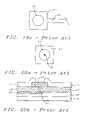
- FIGS. 1 a and 1 bshow a top view and a cross section of a prior art metal bump that is created over the surface of an aluminum pad that has been used as an I/O contact pad during wafer level device testing.
- FIGS. 2 a through 2 dshow a top view and a cross section of the implementation of the first embodiment of the invention, that is the contact pad is completely or partially etched within the opening that has been created in the protective layer of passivation.
- the contact padis contacted by means of interconnect metal (not shown) that has been created in the plane of the contact pad, the interconnect metal is not part of the invention.
- FIGS. 3 a through 3 dshow a top view and a cross section of the implementation of the second embodiment of the invention, that is the contact pad is completely or partially etched.
- the contact padis contacted by means of an array of vias created in the underlying layer of dielectric, this array of vias is not part of the process of the invention.
- FIGS. 4 a through 4 dshow a top view and a cross section of the implementation of the third embodiment of the invention.
- a layer of polyimidehas been added to the structure, the contact pad is completely or partially etched within the opening that has been created in the layer of polyimide.
- the contact padis contacted by means of interconnect metal (not shown) that has been created in the plane of the contact pad, the interconnect metal is not part of the invention.
- FIGS. 5 a through 5 dshow a top view and a cross section of the implementation of the fourth embodiment of the invention.
- a layer of polyimidehas been added to the structure, the contact pad is completely or partially etched.
- the contact padis contacted by means of an array of vias created in the underlying layer of dielectric, this array of vias is not part of the process of the invention.
- FIGS. 6 through 13 baddress the processing steps of the invention whereby no layer of polyimide is used, as follows:
- FIG. 6shows a cross section of a semiconductor surface, a layer of dielectric has been deposited over the semiconductor surface, a contact pad has been provided over a layer of dielectric. A layer of passivation has been deposited, patterned and etched, creating in opening in the layer of passivation that aligns with the contact pad. A probe mark is highlighted.
- FIG. 7shows a cross section after the contact pad has been partially etched using the layer of passivation as a self-aligned etching mask.
- the contact padis contacted by means of interconnect metal (not shown) that has been created in the plane of the contact pad, the interconnect metal is not part of the invention.
- FIG. 8shows a cross section after the contact pad has been partially etched using the layer of passivation as a self-aligned etching mask.
- the contact padis contacted by means of an array of vias created in the underlying layer of dielectric, this array of vias is not part of the process of the invention.
- FIG. 9 ashows a cross section after the contact pad has been completely etched using the layer of passivation as a self-aligned etching mask.
- the contact padis contacted by means of interconnect metal (not shown) that has been created in the plane of the contact pad, the interconnect metal is not part of the invention.
- FIG. 9 bshows a cross section after the contact pad has been completely etched using the layer of passivation as a self-aligned etching mask.
- the contact padis contacted by means of an array of vias created in the underlying layer of dielectric, this array of vias is not part of the process of the invention.
- FIG. 10 ashows a cross section after a layer of UBM has been formed overlying the partially etched contact pad and the layer of passivation of FIG. 7 .
- FIG. 10 bshows a cross section after a layer of UBM has been formed overlying the partially etched contact pads and the layer of passivation.
- the contact padis contacted by means of an array of vias created in the underlying layer of dielectric, this array of vias is not part of the process of the invention.
- FIG. 11 ashows a cross section after a layer of photoresist has been deposited, patterned and etched over the structure of FIG. 10 a , creating an opening in the layer of photoresist that aligns with the contact pad.
- a layer of enhanced UBMhas been deposited over the surface of the layer of UBM.
- FIG. 11 bshows a cross section after a layer of photoresist has been deposited, patterned and etched over the structure of FIG. 10 b , creating an opening in the layer of photoresist that aligns with the contact pad.
- a layer of enhanced UBMhas been deposited over the surface of the layer of UBM.
- FIG. 12 ashows a cross section after a layer of bump metal has been deposited over the layer of enhanced UBM of the structure of FIG. 11 a.
- FIG. 12 bshows a cross section after a layer of bump metal has been deposited over the layer of enhanced UBM of the structure of FIG. 11 b.
- FIG. 13 ashows a cross section after photoresist stripping and etching of the layer of UBM of the structure of FIG. 12 a.
- FIG. 13 bshows a cross section after photoresist stripping and etching of the layer of UBM of the structure of FIG. 12 b.
- FIGS. 14 a through 18 baddress the processing steps of the invention whereby a layer of polyimide is used, as follows:
- FIG. 14 acan be compared with FIG. 7 , a layer of polyimide has been added and patterned to the cross section that is shown in FIG. 14 a .
- the contact padis then either partially or completely etched in accordance with the opening created in the layer of polyimide.
- FIG. 14 bcan be compared with FIG. 8 .
- a layer of polyimidehas been added and patterned to the cross section that is shown in FIG. 14 b .
- the contact padis then either partially or completely etched in accordance with the opening created in the layer of polyimide.
- FIG. 15 acan be compared with FIG. 10 a , a patterned layer of polyimide has been added to the cross section that is shown in FIG. 15 a.
- FIG. 15 bcan be compared with FIG. 10 b , a patterned layer of polyimide has been added to the cross section that is shown in FIG. 15 b.
- FIG. 16 acan be compared with FIG. 11 a , a patterned layer of polyimide has been added to the cross section that is shown in FIG. 16 a.
- FIG. 16 bcan be compared with FIG. 11 b , a patterned layer of polyimide has been added to the cross section that is shown in FIG. 16 b.
- FIG. 17 acan be compared with FIG. 12 a , a patterned layer of polyimide has been added to the cross section that is shown in FIG. 17 a.
- FIG. 17 bcan be compared with FIG. 12 b , a patterned layer of polyimide has been added to the cross section that is shown in FIG. 17 b.
- FIG. 18 acan be compared with FIG. 13 a , a patterned layer of polyimide has been added to the cross section that is shown in FIG. 18 a.
- FIG. 18 bcan be compared with FIG. 13 b , a patterned layer of polyimide has been added to the cross section that is shown in FIG. 18 b.
- FIGS. 19 a through 19 cshow prior art methods of creating a contact pad, the contact pad is contacted by means of interconnect metal that is created in the plane of the contact pad.
- FIGS. 20 a through 20 dshow prior art methods of creating a contact pad, the contact pad is contacted by means of vias that penetrate the layer of dielectric over which the contact pad is deposited.
- Contact padshaving dimensions of about between about 60 ⁇ 60 micrometers and 120 ⁇ 120 micrometers, are in current practice frequently used as access or input/output contact points during wafer level testing of semiconductor devices. In view of the complexity and density of high performance semiconductor devices, these contact pads will, during a complete cycle of testing, by contacted a number of times. Testing is as a matter of economic necessity performed at high speed which frequently results in landing the test probe on the surface of the contact pad at high speed, resulting in mechanical damage to the surface of the contact pad. In a well controlled testing production line, the distribution of the probe marks (or the damaged surface area of the contact pad) is limited (controlled) to an area in the range of about 60 ⁇ 60 micrometers.
- This surfacemay occur in the form of a dent in the surface of the contact pad or may even become severe enough that the surface of the contact pad is broken resulting in the occurrence of burring in the surface of the contact pad.
- probe testingwhich uses bond pads for accessing the devices, must be performed prior to creating wafer solder bumps on the surface of the bond pads, this in order to allow for memory repairs of faulty devices.
- the most recent practiceis for the repair of memory products to be performed by opening (breaking or interrupting) polysilicon fuses using lasers. As indicated above, the testing can cause damage to the surface of the bond pads, creating problems of solder bump and device reliability.
- FIG. 1 ashows a top view of a metal bump structure that is created using current practices.
- FIG. 1 bshows a cross section of the metal bump structure using current practices. It is assumed that the views that are shown in FIGS. 1 a and 1 b relate to an aluminum contact pad that has been used as a point of I/O for testing of a device at the wafer level, using a tester probe to contact the aluminum pad.
- FIG. 1 aShown in FIG. 1 a is a top view of a prior art metal bump having the following elements:
- FIG. 1 bShown in FIG. 1 b is a cross section of a prior art metal bump having the following elements:
- UBMunder-bump-metal
- a layer of metalsuch as copper or nickel, that forms an integral part of the pedestal of the metal bump
- the layer 33 of under bump metalis created overlying the aluminum contact pad 24 .
- the surface of aluminum contact pad 24is not planar (as shown with the probe mark 28 in FIG. 1 b ) and is in many instances disturbed in an unpredictable manner by the tester probe.
- the layer 33 of under bump metaldoes therefore in most cases not fill the damaged surface region 28 of the aluminum pad 24 . This opens the potential for trapping foreign and undesirable materials, such as moisture, a processing gas, a plating solution, solvent and the like, in the unfilled (by the layer 33 of under bump metal) regions in or surrounding the probe mark 28 on the surface of the aluminum pad 24 .
- a contact pad of standard designetching the contact pad and completely or partially removing the aluminum of the contact pad over a surface area of the contact pad that is bounded by the opening that is created in the overlying protective layer of passivation; the metal bump is created filling and overlying the opening that has been created in the layer of passivation.
- the contact padis contacted by means of interconnect metal that is created in the plane of the contact pad, this interconnect metal is not part of the invention
- the contact padis contacted by means of one or more vias that are created penetrating the layer of dielectric over the which the contact pad has been deposited
- the layer of polyimidecan similarly cover and protect fuses during etching in subsequent processing steps.
- FIGS. 2 a through 5 dThese four highlighted approaches are further shown in FIGS. 2 a through 5 d.
- FIG. 2 ashows a top view of the metal bump of the invention that applies to the first embodiment of the invention.
- the contact pad 24is contacted by means of interconnect metal (not shown) that is created in the plane of the contact pad and overlying the surface of layer 29 of dielectric. Shown in FIG. 2 a are:
- the region that is bordered by circumference 27 , FIG. 2 ais the region of the contact pad 24 that is exposed and surrounded by the layer 32 of passivation ( FIG. 2 b ). This surface region is therefore the exposed surface of the contact pad 24 at the time prior to the creation of Under Bump Metal over the surface of the contact pad 24 .
- FIG. 2 bShown in FIG. 2 b are:
- UBMunder-bump-metal
- layer 34a layer of enhanced UBM that forms an integral part of the pedestal of the metal bump; layer 34 serves to enhance adhesion between overlying layers, as a diffusion barrier and to form one of the plates during the process of electroplating
- the layer 32 of passivation that is deposited over the surface of said semiconductor surfacecan comprise a plurality of layers of passivation material.
- the thickness of the contact pad 24has been reduced by a considerable amount over a surface region of the contact pad 24 that is bordered by circumference 27 ( FIG. 2 a ) of the layer 32 of passivation. As shown in the cross section of FIG. 2 b , the contact pad has been reduced to a thickness of about 2000 Angstrom. As one of the solutions to the problem of the probe bump in the surface of the contact pad, the contact pad can also be completely removed within the opening of the layer 32 of passivation, down to the surface of the layer 29 of dielectric. This latter solution has been highlighted in the cross sections that are shown in FIGS. 2 c and 2 d where the contact pad has been etched down to the surface of the layer 29 of dielectric.
- FIGS. 3 a through 3 dshow the solution of the invention whereby the contact pad 24 is contacted by means of an array of vias 11 created in the underlying layer 29 of dielectric.
- the creation of vias 11is not part of the invention.
- the contact padcan be reduced to a thickness of about 2000 Angstrom ( FIG. 3 b ) or the contact pad can be etched down to the surface of the underlying layer 29 of dielectric ( FIG. 3 d ).
- FIG. 4 ashows a top view of the metal bump that is essentially the same as the cross section that is shown in FIG. 2 a with the addition of the line 46 which is the circumference of the opening that has been created in a layer 40 (see FIG. 4 b ) of polyimide that has been added to the structure.
- FIGS. 4 a through 4 daddress the case where the contact pad 24 is contacted by means of interconnect metal (not shown) that is created in the plane of the contact pad and overlying layer 29 of dielectric.
- Layer 40 of polyimideis better visible in the cross section that is shown in FIG. 4 b .
- FIG. 4 bshows a cross section that is essentially the same as the cross section that is shown in FIG.
- the surface of contact pad 24is exposed (surface area 44 of FIGS. 4 a and 4 b ) within the boundaries of the line 46 , this prior to the creation of UBM layers overlying the contact pad 24 .
- the aluminum of the contact pad 24can be etched, as limited by the opening 46 that has been created in the layer 40 of polyimide. The etch can either completely remove the aluminum of the contact pad 24 from above the surface of layer 29 of dielectric ( FIG. 4 d ) or can reduce that thickness of the contact pad 24 to where about 2000 Angstrom of aluminum remains in place on the surface of layer 29 of dielectric ( FIG. 4 b ).
- FIGS. 5 a through 5 dhave been related to FIGS. 2 a through 4 b , so can FIGS. 5 a through 5 d can be related to FIGS. 3 a through 3 d .
- FIG. 5 ashows a top view of the metal bump of the invention that is essentially the same as the top view that is shown in FIG. 3 a with the addition of the line 46 which is the circumference of the opening in a layer 40 of polyimide that has been added to the structure.
- FIGS. 5 a through 5 daddress the case where the contact pad 24 is contacted by means of vias 11 that have been created penetrating the underlying layer 29 of dielectric. The creation of vias 11 is not part of the invention.
- FIG. 5 bshows a cross section that is essentially the same as the cross section that is shown in FIG. 3 b with the addition of a layer 40 of polyimide.
- the surface of contact pad 24is visible (exposed) as bounded by the line 46 , this prior to the creation of UBM layers overlying the contact pad 24 .
- the aluminum of the contact pad 24can be etched, limited by the opening 46 that has been created in the layer 40 of polyimide. The etch can either completely remove the aluminum of the contact pad 24 from above the surface of layer 29 of dielectric or can reduce that thickness of the contact pad 24 to where about 2000 Angstrom of aluminum remains in place on the surface of layer 29 of dielectric.
- polyimide filmsas inter-level dielectrics has been pursued as a technique for providing partial planarization of a dielectric surface.
- the polyimidecovers and protects the fuses, which are used for memory repair, during aluminum etching or during UBM etching in the process of the invention.
- Polyimidesoffer the following characteristics for such applications:
- step heights of underlying featuresare reduced, and step slopes are gentle and smooth.
- the cured polyimide filmscan tolerate temperatures of up to 500 degrees C. without degradation of their dielectric film characteristics.
- polyimide filmshave dielectric breakdowns, which are only slightly lower than that of SiO.sub.2.
- the dielectric constant of polyimidesis smaller than that of silicon nitride and of SiO.sub.2.
- an aluminum contact padis provided over the surface of a layer of dielectric, the layer of dielectric has been deposited on a semiconductor surface, typically the surface of a semiconductor substrate; the creation of the contact pad is not part of the invention
- the surface of the aluminum padis partially exposed, prior to formation of overlying layers of UBM and bump metal, either through an opening that is created in a layer of passivation that has been deposited over the layer of dielectric or through an opening that has been created in a layer of polyimide that has been deposited over the surface of a layer of passivation
- the partially exposed surface of the aluminum padis etched, either completely or partially removing the aluminum from above the surface of the layer of dielectric
- the contact padcan be contacted either by means of interconnect metal (not part of the invention) that is created in the plane of the contact pad and overlying the layer of dielectric above which the contact pad is located or by means of vias (not part of the invention) that are created through the layer of dielectric above which the contact pad is located.
- FIGS. 19 a and 19 b and in FIGS. 20 a through 20 dPrior art methods that are used to create a contact pad are further highlighted in FIGS. 19 a and 19 b and in FIGS. 20 a through 20 d . These figures also address methods that can be used for the interconnection of the contact pad. Although these methods of interconnection of contact pads are not part of the invention, a brief review of these methods at this time is considered of value.
- FIGS. 19 a through 19 caddress the conventional processing sequence that is used to create an aluminum bond pad.
- FIG. 19 atypically the surface of a silicon single crystalline substrate.
- An interconnection scheme 13 ′consisting of one or more layers of metal and Intra Metal Dielectric (IMD) is created over the surface 10 .
- a layer 17 ′ of metal, typically aluminum,is deposited over the surface of the layer 13 ′.
- Layer 17 ′ of aluminumis patterned and etched, typically using a layer of photoresist (not shown in FIG. 19 a ) and conventional methods of photolithography and etching.
- a layer 11 ′ of passivationis deposited over the layer 13 ′.
- FIG. 19 cshows a top view of the contact pad 17 ′, the top view of the contact pad 17 ′ that is shown in FIG. 19 c shows interconnection 19 ′ (to other electrical components) and the opening 15 ′ that is created in the layer 11 ′ of passivation.
- the contact pad that is shown in FIGS. 19 a through 19 cis accessed by means of interconnect metal ( 19 ′) which is created in the plane of the contact pad 17 ′.
- FIGS. 20 a through 20 dAnother approach that is used to access a contact pad is shown in FIGS. 20 a through 20 d .
- the contact pad 17 ′is accessed by means of vias that are in contact with the contact pad.
- FIG. 20 ashows a top view of a contact pad 17 ′ that is exposed through opening 15 ′ in a layer of surrounding passivation.
- via 21 ′that in this case has been created in about the center of opening 15 ′.
- Via 21 ′is more clearly shown in the cross section of FIG. 20 b where also is shown interconnect line 23 ′ that now can be used to connect the contact pad 17 ′ to additional electrical components or interconnect networks.
- Interconnect line 23 ′is in most instances imbedded in a layer 25 ′ of dielectric that overlies a semiconductor surface 10 .
- This method of “vertical” interconnectneed not be limited to one interconnect via 21 ′ but can be extended to include a number of vias, this is shown in top view in FIG. 20 c and in cross section in FIG. 20 d .
- the cross section that is shown in FIG. 20 dis taken along the line d-d′ of FIG. 20 c and shows three of the vias (one via 21 ′ and two vias 27 ′) that have been shown in top view in FIG. 20 c .
- Interconnect line 23 ′in this case is used to establish electrical contact between the contact pad 17 ′ and surrounding electrical components (not shown).
- tungstenis the preferred metal that is used for the creation of metal vias 21 ′ and 27 ′, the contact pad 17 ′ is preferably made using aluminum.
- FIGS. 6 through 13 bfollow the processing sequence that is required to create a metal bump in accordance with the top view and cross section that is shown in FIGS. 2 a through 3 d , that is no layer of polyimide is used for these processing steps.
- FIG. 6shows a cross section of substrate 10 on the surface of which a contact pad has been created, the following elements are highlighted:
- FIG. 7shows a cross section of the substrate 10 after the aluminum contact pad 24 has partially etched in accordance with the opening 36 of the passivation 32 .
- This etch of the aluminum padhas created opening 36 in the aluminum pad 24 and has, as is the objective of the invention, removed the probe mark 28 and the regions surrounding the probe mark 28 from the surface of the aluminum pad 24 .
- the depth of the etch of the aluminum pad 24can be controlled by controlling the etch time. This implies that not all of the aluminum of contact pad 24 has to be removed from the surface of layer 29 of dielectric. As one of the preferred methods of the invention that is shown in FIG.
- FIG. 7shows a layer of aluminum with a thickness of about 2000 Angstrom is left in place over the surface of the layer 29 of dielectric, bounded by the opening 36 of passivation 32 . From this it is clear that, where FIG. 7 shows a layer 48 with a thickness of about 2000 Angstrom, this layer of aluminum may be further removed from the surface of layer 29 of dielectric by continued etching of the contact pad 24 , as shown in FIG. 9 a . It is of interest to note that contact pad 24 remains fully in place where the layer 32 of passivation overlies the contact pad 24 .
- the etching of the aluminum pad 24 in accordance with opening 36can, as previously stated, use methods of plasma enhanced dry etching or wet etching with a H.sub.3PO.sub.4 solution. Other methods for the etching of the aluminum pad have previously been highlighted and equally apply at this stage in the process.
- FIGS. 7 through 9 bTo summarize FIGS. 7 through 9 b:
- FIG. 7shows a cross section where the contact pad has been partially etched, stopping the etch of the aluminum pad 24 at the point where about 2000 Angstrom of aluminum is left in place; the contact pad is contacted by means of interconnect metal (not shown) that is created in the plane of the contact pad
- FIG. 8is identical to FIG. 7 except that for the case that is shown in FIG. 8 the contact pad is contacted by means of vias 11
- FIG. 9 ais identical with FIG. 7 except that the aluminum of the contact pad 24 has been completely removed from above the surface of layer 29 of dielectric in accordance with the opening 36 created in the layer 32 of passivation
- FIG. 9 bis identical with FIG. 8 except that the aluminum of the contact pad 24 has been completely removed from above the surface of layer 29 of dielectric in accordance with the opening 36 created in the layer 32 of passivation.
- FIG. 10 ashows a cross section after the layer 33 of under bump metal (UBM) has been blanket deposited over the surface of the wafer.
- UBMunder bump metal
- Layer 33 of UBMcan be deposited by vacuum evaporation or by sputtering and may contain multiple layers of metal such as a layer of chrome, followed by a layer of copper. From the latter it is apparent that layer 33 of UBM may comprise several layers of metal that are successively deposited.
- any of the conventional UBM materialscan be used.
- a UBM layercan be deposited using a sputter chamber or an Ion Metal Plasma (IMP) chamber, deposited at a temperature of between about 0 and 300 degrees C., a pressure of between about 1 and 100 mTorr, using (for instance) copper or a copper alloy as the source (as highlighted above) at a flow rate of between about 10 and 400 sccm and using argon as an ambient gas.
- IMPIon Metal Plasma
- layer 48may have been completely removed by extended etching of the contact pad 24 , as previously indicated.
- This layer 48has been shown in FIG. 10 a as being etched down to about 2000 Angstrom, if this layer has been completely removed from above the layer 29 of dielectric, the layer 33 of UBM is deposited directly on the surface of layer 29 of dielectric.
- FIG. 10 bshows a cross section after the layer 33 of under bump metal (UBM) has been deposited over the surface that is shown in cross section of FIG. 8 , that is the embodiment of the invention where vias through the layer 29 of dielectric as used to make contact with contact pad 24 .
- UBMunder bump metal
- FIG. 11 ais a continuation of FIG. 10 a and shows how a layer 39 of photoresist has been deposited over the layer 33 of UBM.
- Layer 39 of photoresistis patterned and developed, creating an opening 38 in the layer 39 of photoresist that is slightly wider than the opening of the bonding pad of the to be created solder bump.
- a layer 34 of enhanced UBMtypically of copper or nickel and of a thickness between about 1 and 10 micrometers is electroplated over the layer 33 of UBM.
- the UBM layer 33serves as the common electrode for the electroplating process with the layer of photoresist still being in place.
- layer 48although this layer is shown in this cross section, may in fact have been removed completely from the surface of the dielectric layer 29 .
- FIG. 11 bThe cross section that is shown in FIG. 11 b will be recognized as a continuation of the cross section shown in FIG. 10 b .
- the cross section of FIG. 11 bis created by applying processing steps (to the cross section of FIG. 10 b ) that are identical to the processing steps that have been applied to create FIG. 11 a (from the cross section shown in FIG. 10 a ). Where therefore FIG. 11 a is a continuation of FIG. 10 a , FIG. 11 b is a continuation of FIG. 10 b . All the remarks that have been provided relating to FIG. 11 a can also be made with respect to FIG. 11 b , FIG. 11 b is shown since the vias are present in this cross section.
- the layer 35 of bump metal(typically solder or gold) is electroplated in contact with the layer 34 of enhanced UBM, this is shown in cross section in both FIG. 12 a (for the case where the contact pad is accessed by interconnect metal created in the plane of the contact pad) and in FIG. 12 b (for the case where vias 11 have been provided through the underlying layer of dielectric). It must again be pointed out, with respect to both FIG. 12 a and FIG. 12 b , that layer 48 , although shown in cross section in these figures, may have been completely removed from the surface of layer 29 of dielectric.
- bump metaltypically solder or gold
- the layer 35 of electroplated metalis centered in the opening 38 ( FIGS. 12 a and 12 b ) that has been created in the layer 39 of photoresist.
- FIGS. 13 a and 13 bshow a cross section after the layer 39 ( FIGS. 12 a and 12 b ) of photoresist has been removed.
- the layer 33 of UBMhas been etched using the patterned layer 35 of electroplated metal as a mask.
- processing steps of electroplating that are used for the creation of a metal bumpcan be supplemented by the step of curing or pre-baking of the layers of photoresist after these layers have been deposited.
- the inventioncan also be applied to other processes that are used to create solder bumps such as screen printing and stencil printing.
- FIGS. 6 through 13 bhave shown the metal bump of the invention that does not make use of a layer of polyimide
- the following drawingsaddress the metal bump of the invention that does make use of a layer of polyimide.
- Layer 50has been patterned and etched, using conventional methods, creating opening 36 ′ in the layer of polyimide. What must be remarked in this respect is that the diameter of opening 36 ′ can be slightly or even significantly smaller than the diameter of the opening 36 ( FIG. 7 ) that has been created in the layer 32 of passivation. The opening 36 ′ should cover the probe mark 28 .
- FIG. 8 and FIG. 14 balso results from the deposition of a layer of polyimide over the surface of the passivation layer 32 ( FIG. 14 b ).
- Layer 50( FIG.
- opening 36 ′has been patterned and etched, using conventional methods, creating opening 36 ′ in the layer of polyimide with a diameter of opening 36 ′ that is slightly or significantly smaller than the diameter of the opening 36 ( FIG. 8 ).
- the opening 36 ′should cover the probe mark 28 .
- the layer of polyimideis very important because the polyimide covers fuses in order to prevent exposure of the fuses during subsequent etching of the damaged contact pads.
- a first chip probe test(CP 1 ) is performed
- CP 2a second chip probe test
- the deposited layer of polyimideis patterned, creating openings to the contact pad, the aluminum pad is at this time partially or completely removed by etching
- FIG. 14 acan be compared with FIG. 7 , a patterned layer 50 of polyimide has been added to the cross section that is shown in FIG. 14 a.
- FIG. 14 bcan be compared with FIG. 8 , a patterned layer 50 of polyimide has been added to the cross section that is shown in FIG. 14 b.
- FIG. 15 acan be compared with FIG. 10 a , a patterned layer 50 of polyimide has been added to the cross section that is shown in FIG. 15 a.
- FIG. 15 bcan be compared with FIG. 10 b , a patterned layer 50 of polyimide has been added to the cross section that is shown in FIG. 15 b.
- FIG. 16 acan be compared with FIG. 11 a , a patterned layer 50 of polyimide has been added to the cross section that is shown in FIG. 16 a.
- FIG. 16 bcan be compared with FIG. 11 b , a patterned layer 50 of polyimide has been added to the cross section that is shown in FIG. 16 b.
- FIG. 17 acan be compared with FIG. 12 a , a patterned layer 50 of polyimide has been added to the cross section that is shown in FIG. 17 a.
- FIG. 17 bcan be compared with FIG. 12 b , a patterned layer 50 of polyimide has been added to the cross section that is shown in FIG. 17 b.
- FIG. 18 acan be compared with FIG. 13 a , a patterned layer 50 of polyimide has been added to the cross section that is shown in FIG. 18 a.
- FIG. 18 bcan be compared with FIG. 13 b , a patterned layer 50 of polyimide has been added to the cross section that is shown in FIG. 18 b.
- the cross section that is shown in FIG. 4 bcan be achieved by forming the metal bump 35 by reflowing the metal bump layer 35 that is shown in FIG. 18 a.
- the cross section that is shown in FIG. 5 bcan be achieved by forming the metal bump 35 by reflowing the metal bump layer 35 that is shown in FIG. 18 b.
- the inventionstarts with a semiconductor surface, a layer of dielectric has been deposited over the semiconductor surface, a contact pad has been provided on the layer of dielectric, the contact pad has served as an Input/Output (I/O) point of contact during semiconductor device testing, the contact pad is assumed to be connected to at least one point of electrical contact provided in or on the surface of the substrate, the at least one point of electrical contact is assumed to be connected to at least one semiconductor device having been provided in or on the surface of the substrate, the contact pad having an exposed surface
- a layer of passivationis deposited over a semiconductor surface including the surface of said contact pad
- the layer of passivationis patterned and etched, creating an opening in the layer of passivation having a first diameter, partially exposing the surface of the contact pad over a surface area of the first diameter, the opening in the layer of passivation being centered with respect to the contact pad
- the contact padis completely or partially etched in accordance with the opening created in the passivation layer, either leaving a thin layer of aluminum in place or partially exposing the surface of the layer of dielectric deposited over the surface of the substrate
- UBMUnder Bump Metallurgy
- a layer of photoresistis deposited over the semiconductor surface of the layer of UBM
- the layer of photoresistis patterned and etched, creating an opening in the layer of photoresist that is aligned with the contact pad, partially exposing the surface of the layer of UBM
- the exposed surface of the layer of UBMis electroplated with a layer of enhanced UBM
- the layer of enhanced UBMis electroplated with a thick layer of bump metal, partially filling the opening created in the layer of photoresist
- the patterned and etched layer of photoresistis removed from above the semiconductor surface
- the layer of UBMis etched using the deposited layer of bump metal as a mask
- the surface of said layer of bump metalis reflowed, forming the metal bump.
- a layer of polyimidemay be deposited over the layer of passivation, patterned and etched, creating an opening in the layer of polyimide that has a diameter which is slightly or significantly smaller than the diameter of the opening created in the layer of passivation. The created opening is larger than the size of the probe mark. Processing, after the opening has been created in the layer of polyimide, is the same as the processing that is performed (without the layer of polyimide) after an opening has been created in the layer of passivation.
Landscapes
- Engineering & Computer Science (AREA)
- Computer Hardware Design (AREA)
- Microelectronics & Electronic Packaging (AREA)
- Power Engineering (AREA)
- Manufacturing & Machinery (AREA)
- Internal Circuitry In Semiconductor Integrated Circuit Devices (AREA)
Abstract
Description
- This application is a continuation of application Ser. No. 10/962,964, filed on Oct. 12, 2004, now pending.
- This application is related to attorney docket number MEG01-001, filed on Jan. 16, 2001, Ser. No. 09/760,909, assigned to a common assignee.
- (1) Field of the Invention
- The invention relates to the fabrication of integrated circuit devices, and more particularly, to a method of removing damage to I/O pads that have been repetitively contacted and possibly damaged by test probes, thereby avoiding potential solder bump reliability problems.
- (2) Description of the Prior Art
- In creating semiconductor devices, the technology of interconnecting devices and device features is a continuing challenge in the era of sub-micron devices. Bond pads are frequently used for this purpose, whereby continuous effort is dedicated to creating bond pads that are simple, reliable and inexpensive.
- Bond pads are generally used to wire device elements and to provide exposed contact regions of the die. These contact regions are suitable for wiring the die to components that are external to the die. An example is where a bond wire is attached to a bond pad of a semiconductor die at one end and to a portion of a Printed Circuit Board at the other end of the wire. The art is constantly striving to achieve improvements in the creation of bond pads that simplify the manufacturing process while enhancing bond pad reliability.
- A frequently used bond pad consists of an exposed aluminum pad. A gold bond wire can be bonded to this aluminum pad. Materials that are typically used for bond pads include metallic materials, such as tungsten and aluminum, while heavily doped polysilicon can also be used for contacting material. The bond pad is formed on the top surface of the semiconductor device whereby the electrically conducting material is frequently embedded in an insulating layer of dielectric.
- Contact pads, having dimensions of between about 40×40 micrometers and 120×120 micrometers, are in current practice frequently used as access or input/output contact points during wafer level testing of semiconductor devices. In view of the complexity and density of high performance semiconductor devices, these contact pads will, during a complete cycle of testing, be contacted a number of times. Testing is, as a matter of economic necessity, performed at high speed, which frequently results in landing the test probe on the surface of the contact pad at high speed, resulting in mechanical damage (in the form of probe marks) to the surface of the contact pad. Especially for memory products, a wafer is tested at least two times, that is before and after repair of faulty (weak or bad) memory lines. The distribution of the location of the probe mark over the surface of the contact pad is, in a well controlled testing production line, limited to a surface area of about 60×60 micrometers. Surface damage to the contact pad may occur in the form of a dent (in the surface of the contact pad) or may even become severe enough that the surface of the contact pad is disrupted, resulting in the occurrence of burring in the surface of the contact pad. After the contact pads have in this manner been used as an I/O point for accessing the semiconductor device during high speed testing, a number of these contact pads are frequently used for the creation of solder bumps or gold bumps over the surface thereof. In instances where the surface of the contact pad is damaged, it is clear that the surface of the contact pad forms a poor basis on which to create a solder bump or a gold bump. The invention addresses this concern and provides a method whereby surface damage to contact pads is removed.
- U.S. Pat. No. 6,162,652 (Dass et al.) provides for the testing of an integrated circuit device including depositing a solder bump on a surface of a bond pad.
- U.S. Pat. No. 5,756,370 (Farnworth et al.) provides a compliant contact system for making temporary connection with a semiconductor die for testing and a method for fabricating the pliable contact system.
- U.S. Pat. No. 5,554,940 (Hubacker) addresses the probing of semiconductor devices that have been provided with contact bumps and the formation of peripheral test pads.
- A principle objective of the invention is to eliminate the effect of surface damage to I/O pads that has been caused by using these I/O pads as contact points for wafer level testing of semiconductor devices.
- Another objective of the invention is to eliminate the effect of probe marks on the surface of I/O pads for I/O pads that have been used as contact points for wafer level testing of semiconductor devices.
- In accordance with the objectives of the invention a new method is provided for the creation of metal bumps over surfaces of I/O pads. Contact pads are provided over the surface of a layer of dielectric. The aluminum of the I/O pads, which have been used as I/O pads during wafer level semiconductor device testing, is completely or partially removed over a surface area that is equal to or smaller than the surface area of the contact pad using methods of metal dry etching or wet etching. The contact pad can be accessed either by interconnect metal created in a plane of the contact pad or by vias that are provided through the layer of dielectric over which the contact pad has been deposited. The process can be further extended by the deposition, patterning and etching of a layer of polyimide over the layer of passivation that serves to protect the contact pad.
FIGS. 1 aand1bshow a top view and a cross section of a prior art metal bump that is created over the surface of an aluminum pad that has been used as an I/O contact pad during wafer level device testing.FIGS. 2 athrough2dshow a top view and a cross section of the implementation of the first embodiment of the invention, that is the contact pad is completely or partially etched within the opening that has been created in the protective layer of passivation. The contact pad is contacted by means of interconnect metal (not shown) that has been created in the plane of the contact pad, the interconnect metal is not part of the invention.FIGS. 3 athrough3dshow a top view and a cross section of the implementation of the second embodiment of the invention, that is the contact pad is completely or partially etched. The contact pad is contacted by means of an array of vias created in the underlying layer of dielectric, this array of vias is not part of the process of the invention.FIGS. 4 athrough4dshow a top view and a cross section of the implementation of the third embodiment of the invention. A layer of polyimide has been added to the structure, the contact pad is completely or partially etched within the opening that has been created in the layer of polyimide. The contact pad is contacted by means of interconnect metal (not shown) that has been created in the plane of the contact pad, the interconnect metal is not part of the invention.FIGS. 5 athrough5dshow a top view and a cross section of the implementation of the fourth embodiment of the invention. A layer of polyimide has been added to the structure, the contact pad is completely or partially etched. The contact pad is contacted by means of an array of vias created in the underlying layer of dielectric, this array of vias is not part of the process of the invention.FIGS. 6 through 13 baddress the processing steps of the invention whereby no layer of polyimide is used, as follows:FIG. 6 shows a cross section of a semiconductor surface, a layer of dielectric has been deposited over the semiconductor surface, a contact pad has been provided over a layer of dielectric. A layer of passivation has been deposited, patterned and etched, creating in opening in the layer of passivation that aligns with the contact pad. A probe mark is highlighted.FIG. 7 shows a cross section after the contact pad has been partially etched using the layer of passivation as a self-aligned etching mask. The contact pad is contacted by means of interconnect metal (not shown) that has been created in the plane of the contact pad, the interconnect metal is not part of the invention.FIG. 8 shows a cross section after the contact pad has been partially etched using the layer of passivation as a self-aligned etching mask. The contact pad is contacted by means of an array of vias created in the underlying layer of dielectric, this array of vias is not part of the process of the invention.FIG. 9 ashows a cross section after the contact pad has been completely etched using the layer of passivation as a self-aligned etching mask. The contact pad is contacted by means of interconnect metal (not shown) that has been created in the plane of the contact pad, the interconnect metal is not part of the invention.FIG. 9 bshows a cross section after the contact pad has been completely etched using the layer of passivation as a self-aligned etching mask. The contact pad is contacted by means of an array of vias created in the underlying layer of dielectric, this array of vias is not part of the process of the invention.FIG. 10 ashows a cross section after a layer of UBM has been formed overlying the partially etched contact pad and the layer of passivation ofFIG. 7 .FIG. 10 bshows a cross section after a layer of UBM has been formed overlying the partially etched contact pads and the layer of passivation. The contact pad is contacted by means of an array of vias created in the underlying layer of dielectric, this array of vias is not part of the process of the invention.FIG. 11 ashows a cross section after a layer of photoresist has been deposited, patterned and etched over the structure ofFIG. 10 a, creating an opening in the layer of photoresist that aligns with the contact pad. A layer of enhanced UBM has been deposited over the surface of the layer of UBM.FIG. 11 bshows a cross section after a layer of photoresist has been deposited, patterned and etched over the structure ofFIG. 10 b, creating an opening in the layer of photoresist that aligns with the contact pad. A layer of enhanced UBM has been deposited over the surface of the layer of UBM.FIG. 12 ashows a cross section after a layer of bump metal has been deposited over the layer of enhanced UBM of the structure ofFIG. 11 a.FIG. 12 bshows a cross section after a layer of bump metal has been deposited over the layer of enhanced UBM of the structure ofFIG. 11 b.FIG. 13 ashows a cross section after photoresist stripping and etching of the layer of UBM of the structure ofFIG. 12 a.FIG. 13 bshows a cross section after photoresist stripping and etching of the layer of UBM of the structure ofFIG. 12 b.FIGS. 14 athrough18baddress the processing steps of the invention whereby a layer of polyimide is used, as follows:FIG. 14 acan be compared withFIG. 7 , a layer of polyimide has been added and patterned to the cross section that is shown inFIG. 14 a. The contact pad is then either partially or completely etched in accordance with the opening created in the layer of polyimide.FIG. 14 bcan be compared withFIG. 8 . A layer of polyimide has been added and patterned to the cross section that is shown inFIG. 14 b. The contact pad is then either partially or completely etched in accordance with the opening created in the layer of polyimide.FIG. 15 acan be compared withFIG. 10 a, a patterned layer of polyimide has been added to the cross section that is shown inFIG. 15 a.FIG. 15 bcan be compared withFIG. 10 b, a patterned layer of polyimide has been added to the cross section that is shown inFIG. 15 b.FIG. 16 acan be compared withFIG. 11 a, a patterned layer of polyimide has been added to the cross section that is shown inFIG. 16 a.FIG. 16 bcan be compared withFIG. 11 b, a patterned layer of polyimide has been added to the cross section that is shown inFIG. 16 b.FIG. 17 acan be compared withFIG. 12 a, a patterned layer of polyimide has been added to the cross section that is shown inFIG. 17 a.FIG. 17 bcan be compared withFIG. 12 b, a patterned layer of polyimide has been added to the cross section that is shown inFIG. 17 b.FIG. 18 acan be compared withFIG. 13 a, a patterned layer of polyimide has been added to the cross section that is shown inFIG. 18 a.FIG. 18 bcan be compared withFIG. 13 b, a patterned layer of polyimide has been added to the cross section that is shown inFIG. 18 b.FIGS. 19 athrough19cshow prior art methods of creating a contact pad, the contact pad is contacted by means of interconnect metal that is created in the plane of the contact pad.FIGS. 20 athrough20dshow prior art methods of creating a contact pad, the contact pad is contacted by means of vias that penetrate the layer of dielectric over which the contact pad is deposited.- Contact pads, having dimensions of about between about 60×60 micrometers and 120×120 micrometers, are in current practice frequently used as access or input/output contact points during wafer level testing of semiconductor devices. In view of the complexity and density of high performance semiconductor devices, these contact pads will, during a complete cycle of testing, by contacted a number of times. Testing is as a matter of economic necessity performed at high speed which frequently results in landing the test probe on the surface of the contact pad at high speed, resulting in mechanical damage to the surface of the contact pad. In a well controlled testing production line, the distribution of the probe marks (or the damaged surface area of the contact pad) is limited (controlled) to an area in the range of about 60×60 micrometers. This surface may occur in the form of a dent in the surface of the contact pad or may even become severe enough that the surface of the contact pad is broken resulting in the occurrence of burring in the surface of the contact pad. After the contact pads have in this manner been used as I/O points during high speed testing, a number of these contact pads are frequently used for the creation of solder or gold bumps over the surface thereof. In instances where the surface of the contact pad is damaged, it is clear that the surface of the contact pad forms a poor basis on which to create a solder bump or a gold bump. The invention addresses this concern and provides a method whereby surface damage to contact pads is removed.
- For memory products, such as SRAM devices, probe testing which uses bond pads for accessing the devices, must be performed prior to creating wafer solder bumps on the surface of the bond pads, this in order to allow for memory repairs of faulty devices. The most recent practice is for the repair of memory products to be performed by opening (breaking or interrupting) polysilicon fuses using lasers. As indicated above, the testing can cause damage to the surface of the bond pads, creating problems of solder bump and device reliability.
- This is further highlighted in
FIGS. 1 aand1b.FIG. 1 ashows a top view of a metal bump structure that is created using current practices.FIG. 1 bshows a cross section of the metal bump structure using current practices. It is assumed that the views that are shown inFIGS. 1 aand1brelate to an aluminum contact pad that has been used as a point of I/O for testing of a device at the wafer level, using a tester probe to contact the aluminum pad. - Shown in
FIG. 1 ais a top view of a prior art metal bump having the following elements: - 24, an aluminum contact pad
- 25, the circumference of a metal bump overlying
aluminum contact pad 24 - 27, the circumference of the opening created in the
protective layer 32 of passivation (seeFIG. 1 b) - 28, a probe mark caused by a tester probe (not shown) in the surface of
aluminum contact pad 24. - Shown in
FIG. 1 bis a cross section of a prior art metal bump having the following elements: - 10, the silicon substrate over which the aluminum contact pad has been created
- 24, an aluminum contact pad
- 28, the probe mark or bump that has been created in the surface of the
aluminum contact pad 24 by the tester probe (not shown) - 29, a layer of dielectric that has been deposited over the surface of
substrate 10; - 32, a layer of passivation that has been deposited over the surface of the
layer 29 of dielectric; an opening (with acircumference 27, as shown inFIG. 1 a) has been created in thelayer 32 of passivation - 33, a layer of under-bump-metal (UBM) overlying the
aluminum pad 24 - 20, a layer of metal, such as copper or nickel, that forms an integral part of the pedestal of the metal bump
- 35, the metal bump created overlying the
aluminum contact pad 24. - From the above it must be understood that, after the testing has been completed, the
layer 33 of under bump metal is created overlying thealuminum contact pad 24. The surface ofaluminum contact pad 24 is not planar (as shown with theprobe mark 28 inFIG. 1 b) and is in many instances disturbed in an unpredictable manner by the tester probe. Thelayer 33 of under bump metal does therefore in most cases not fill the damagedsurface region 28 of thealuminum pad 24. This opens the potential for trapping foreign and undesirable materials, such as moisture, a processing gas, a plating solution, solvent and the like, in the unfilled (by thelayer 33 of under bump metal) regions in or surrounding theprobe mark 28 on the surface of thealuminum pad 24. - The invention addresses the above detailed problems that are encountered in contact pads by providing the following solutions:
- 1) a contact pad of standard design, etching the contact pad and completely or partially removing the aluminum of the contact pad over a surface area of the contact pad that is bounded by the opening that is created in the overlying protective layer of passivation; the metal bump is created filling and overlying the opening that has been created in the layer of passivation. The contact pad is contacted by means of interconnect metal that is created in the plane of the contact pad, this interconnect metal is not part of the invention
- 2) as highlighted under 1) above, in this case the contact pad is contacted by means of one or more vias that are created penetrating the layer of dielectric over the which the contact pad has been deposited
- 3) the design as indicated above under 1) whereby an extra layer of polyimide has been added to the design of the contact bump; the opening that is created in the layer of polyimide replaces the previously used opening in the layer of passivation in providing the boundaries for etching the contact pad. This layer of polyimide is extremely important especially for memory products in applications where fuse repair is required. The polyimide covers and protects fuses during subsequent etching processes, such as for instance contact pad etching
- 4) the design as indicated above under 2) whereby an extra layer of polyimide has been added to the design of the contact bump; the opening that is created in the layer of polyimide replaces the previously used opening in the layer of passivation in providing the boundaries for etching the contact pad. The layer of polyimide can similarly cover and protect fuses during etching in subsequent processing steps.
- These four highlighted approaches are further shown in
FIGS. 2 athrough5d. FIG. 2 ashows a top view of the metal bump of the invention that applies to the first embodiment of the invention. Thecontact pad 24 is contacted by means of interconnect metal (not shown) that is created in the plane of the contact pad and overlying the surface oflayer 29 of dielectric. Shown inFIG. 2 aare:- 24, an aluminum contact pad
- 25, the circumference of a metal bump created overlying
aluminum contact pad 24 - 27, the circumference of the opening that is created in an overlying
protective layer 32 of passivation, seeFIG. 2 b - 28, the region in the surface of the
aluminum contact pad 24 where a probe mark has been left by the tester probe. - It must be noted that the region that is bordered by
circumference 27,FIG. 2 a, is the region of thecontact pad 24 that is exposed and surrounded by thelayer 32 of passivation (FIG. 2 b). This surface region is therefore the exposed surface of thecontact pad 24 at the time prior to the creation of Under Bump Metal over the surface of thecontact pad 24. - Shown in
FIG. 2 bare: - 10, the silicon substrate over which the aluminum contact pad has been created
- 24, an aluminum contact pad
- 29, a layer of dielectric deposited over the surface of
substrate 10; - 32, a layer of passivation deposited over the surface of the
layer 29 of dielectric; an opening has been created in thelayer 32 of passivation - 33, a layer of under-bump-metal (UBM) overlying the
aluminum pad 24 - 34, a layer of enhanced UBM that forms an integral part of the pedestal of the metal bump;
layer 34 serves to enhance adhesion between overlying layers, as a diffusion barrier and to form one of the plates during the process of electroplating - 35, the metal bump created overlying the
aluminum contact pad 24. - It must be understood that the
layer 32 of passivation that is deposited over the surface of said semiconductor surface can comprise a plurality of layers of passivation material. - Notable in the cross section that is shown in
FIG. 2 bis that the thickness of thecontact pad 24 has been reduced by a considerable amount over a surface region of thecontact pad 24 that is bordered by circumference27 (FIG. 2 a) of thelayer 32 of passivation. As shown in the cross section ofFIG. 2 b, the contact pad has been reduced to a thickness of about 2000 Angstrom. As one of the solutions to the problem of the probe bump in the surface of the contact pad, the contact pad can also be completely removed within the opening of thelayer 32 of passivation, down to the surface of thelayer 29 of dielectric. This latter solution has been highlighted in the cross sections that are shown inFIGS. 2 cand2dwhere the contact pad has been etched down to the surface of thelayer 29 of dielectric. FIGS. 3 athrough3dshow the solution of the invention whereby thecontact pad 24 is contacted by means of an array ofvias 11 created in theunderlying layer 29 of dielectric. The creation ofvias 11 is not part of the invention. As in the solution that is shown inFIGS. 2 athrough2d, the contact pad can be reduced to a thickness of about 2000 Angstrom (FIG. 3 b) or the contact pad can be etched down to the surface of theunderlying layer 29 of dielectric (FIG. 3 d).FIG. 4 ashows a top view of the metal bump that is essentially the same as the cross section that is shown inFIG. 2 awith the addition of theline 46 which is the circumference of the opening that has been created in a layer40 (seeFIG. 4 b) of polyimide that has been added to the structure.FIGS. 4 athrough4daddress the case where thecontact pad 24 is contacted by means of interconnect metal (not shown) that is created in the plane of the contact pad andoverlying layer 29 of dielectric.Layer 40 of polyimide is better visible in the cross section that is shown inFIG. 4 b.FIG. 4 bshows a cross section that is essentially the same as the cross section that is shown inFIG. 2 bwith the addition of alayer 40 of polyimide. The surface ofcontact pad 24 is exposed (surface area 44 ofFIGS. 4 aand4b) within the boundaries of theline 46, this prior to the creation of UBM layers overlying thecontact pad 24. The aluminum of thecontact pad 24 can be etched, as limited by theopening 46 that has been created in thelayer 40 of polyimide. The etch can either completely remove the aluminum of thecontact pad 24 from above the surface oflayer 29 of dielectric (FIG. 4 d) or can reduce that thickness of thecontact pad 24 to where about 2000 Angstrom of aluminum remains in place on the surface oflayer 29 of dielectric (FIG. 4 b).- As
FIGS. 4 athrough4dhave been related toFIGS. 2 athrough4b, so canFIGS. 5 athrough5dcan be related toFIGS. 3 athrough3d.FIG. 5 ashows a top view of the metal bump of the invention that is essentially the same as the top view that is shown inFIG. 3 awith the addition of theline 46 which is the circumference of the opening in alayer 40 of polyimide that has been added to the structure.FIGS. 5 athrough5daddress the case where thecontact pad 24 is contacted by means ofvias 11 that have been created penetrating theunderlying layer 29 of dielectric. The creation ofvias 11 is not part of the invention. Thislayer 40 of polyimide is again better visible in the cross section that is shown inFIG. 5 b.FIG. 5 bshows a cross section that is essentially the same as the cross section that is shown inFIG. 3 bwith the addition of alayer 40 of polyimide. The surface ofcontact pad 24 is visible (exposed) as bounded by theline 46, this prior to the creation of UBM layers overlying thecontact pad 24. The aluminum of thecontact pad 24 can be etched, limited by theopening 46 that has been created in thelayer 40 of polyimide. The etch can either completely remove the aluminum of thecontact pad 24 from above the surface oflayer 29 of dielectric or can reduce that thickness of thecontact pad 24 to where about 2000 Angstrom of aluminum remains in place on the surface oflayer 29 of dielectric. - It must be noted that the use of polyimide films as inter-level dielectrics has been pursued as a technique for providing partial planarization of a dielectric surface. For memory products, the polyimide covers and protects the fuses, which are used for memory repair, during aluminum etching or during UBM etching in the process of the invention. Polyimides offer the following characteristics for such applications:
- they produce surfaces in which the step heights of underlying features are reduced, and step slopes are gentle and smooth.
- they are available to fill small openings without producing the voids that occur when low-temperature CVD oxide films are deposited.
- the cured polyimide films can tolerate temperatures of up to 500 degrees C. without degradation of their dielectric film characteristics.
- polyimide films have dielectric breakdowns, which are only slightly lower than that of SiO.sub.2.
- the dielectric constant of polyimides is smaller than that of silicon nitride and of SiO.sub.2.
- the process used to deposit and pattern polyimide films is relatively simple.
- To summarize the invention:
- an aluminum contact pad is provided over the surface of a layer of dielectric, the layer of dielectric has been deposited on a semiconductor surface, typically the surface of a semiconductor substrate; the creation of the contact pad is not part of the invention
- the surface of the aluminum pad is partially exposed, prior to formation of overlying layers of UBM and bump metal, either through an opening that is created in a layer of passivation that has been deposited over the layer of dielectric or through an opening that has been created in a layer of polyimide that has been deposited over the surface of a layer of passivation
- the partially exposed surface of the aluminum pad is etched, either completely or partially removing the aluminum from above the surface of the layer of dielectric
- the contact pad can be contacted either by means of interconnect metal (not part of the invention) that is created in the plane of the contact pad and overlying the layer of dielectric above which the contact pad is located or by means of vias (not part of the invention) that are created through the layer of dielectric above which the contact pad is located.
- Prior art methods that are used to create a contact pad are further highlighted in
FIGS. 19 aand19band inFIGS. 20 athrough20d. These figures also address methods that can be used for the interconnection of the contact pad. Although these methods of interconnection of contact pads are not part of the invention, a brief review of these methods at this time is considered of value. FIGS. 19 athrough19caddress the conventional processing sequence that is used to create an aluminum bond pad.- The process starts with a
semiconductor surface 10,FIG. 19 a, typically the surface of a silicon single crystalline substrate. Aninterconnection scheme 13′ consisting of one or more layers of metal and Intra Metal Dielectric (IMD) is created over thesurface 10. Alayer 17′ of metal, typically aluminum, is deposited over the surface of thelayer 13′.Layer 17′ of aluminum is patterned and etched, typically using a layer of photoresist (not shown inFIG. 19 a) and conventional methods of photolithography and etching. After thebond pad 17′,FIG. 19 b, has been created in this manner, and afterinterconnect 19′ has been created, alayer 11′ of passivation is deposited over thelayer 13′. Anopening 15′ that aligns with thebond pad 17′ is created in thelayer 11′ of passivation, again using methods of photolithography and etching. Shown in cross section inFIG. 19 biselement 19′, which represents one method of connecting thecontact pad 17′ to surrounding circuit elements.FIG. 19 cshows a top view of thecontact pad 17′, the top view of thecontact pad 17′ that is shown inFIG. 19 cshowsinterconnection 19′ (to other electrical components) and theopening 15′ that is created in thelayer 11′ of passivation. The contact pad that is shown inFIGS. 19 athrough19cis accessed by means of interconnect metal (19′) which is created in the plane of thecontact pad 17′. - Another approach that is used to access a contact pad is shown in
FIGS. 20 athrough20d. Using this approach, thecontact pad 17′ is accessed by means of vias that are in contact with the contact pad.FIG. 20 ashows a top view of acontact pad 17′ that is exposed through opening15′ in a layer of surrounding passivation. Also shown inFIG. 20 ais via21′ that in this case has been created in about the center of opening15′. Via21′ is more clearly shown in the cross section ofFIG. 20 bwhere also is showninterconnect line 23′ that now can be used to connect thecontact pad 17′ to additional electrical components or interconnect networks.Interconnect line 23′ is in most instances imbedded in alayer 25′ of dielectric that overlies asemiconductor surface 10. This method of “vertical” interconnect need not be limited to one interconnect via21′ but can be extended to include a number of vias, this is shown in top view inFIG. 20 cand in cross section inFIG. 20 d. The cross section that is shown inFIG. 20 dis taken along the line d-d′ ofFIG. 20 cand shows three of the vias (one via21′ and twovias 27′) that have been shown in top view inFIG. 20 c.Interconnect line 23′ in this case is used to establish electrical contact between thecontact pad 17′ and surrounding electrical components (not shown). For most present day applications, tungsten is the preferred metal that is used for the creation of metal vias21′ and27′, thecontact pad 17′ is preferably made using aluminum. - The above has been highlighted in some depth in order to establish that the invention starts after a contact has been created. This contact pad may be accessed in any of the methods that been highlighted above, any processing that is provided by the invention therefore does not concern itself with the creation of vias to which the contact pad is connected or with the creation of interconnect metal in the plane of the contact pad.
- Processing steps that are required to implement the invention are described next.
FIGS. 6 through 13 bfollow the processing sequence that is required to create a metal bump in accordance with the top view and cross section that is shown inFIGS. 2 athrough3d, that is no layer of polyimide is used for these processing steps. FIG. 6 shows a cross section ofsubstrate 10 on the surface of which a contact pad has been created, the following elements are highlighted:- 10, a silicon substrate over the surface of which an aluminum contact pad has been created
- 24, the aluminum contact pad
- 28, the probe mark or bump that has been created in surface of the
aluminum contact pad 24 by repetitive contacting of thecontact pad 24 by a tester probe (not shown) - 29, a layer of dielectric that has been deposited over the surface of
substrate 10 - 32, a layer of passivation that has been deposited over the surface of the
layer 29 of dielectric. An opening has been created in thelayer 32 of passivation that aligns with thealuminum contact pad 24, partially exposing the surface of thecontact pad 24. FIG. 7 shows a cross section of thesubstrate 10 after thealuminum contact pad 24 has partially etched in accordance with theopening 36 of thepassivation 32. This etch of the aluminum pad has createdopening 36 in thealuminum pad 24 and has, as is the objective of the invention, removed theprobe mark 28 and the regions surrounding theprobe mark 28 from the surface of thealuminum pad 24. The depth of the etch of thealuminum pad 24 can be controlled by controlling the etch time. This implies that not all of the aluminum ofcontact pad 24 has to be removed from the surface oflayer 29 of dielectric. As one of the preferred methods of the invention that is shown inFIG. 7 , a layer of aluminum with a thickness of about 2000 Angstrom is left in place over the surface of thelayer 29 of dielectric, bounded by theopening 36 ofpassivation 32. From this it is clear that, whereFIG. 7 shows alayer 48 with a thickness of about 2000 Angstrom, this layer of aluminum may be further removed from the surface oflayer 29 of dielectric by continued etching of thecontact pad 24, as shown inFIG. 9 a. It is of interest to note thatcontact pad 24 remains fully in place where thelayer 32 of passivation overlies thecontact pad 24.- The etching of the
aluminum pad 24 in accordance with opening36 can, as previously stated, use methods of plasma enhanced dry etching or wet etching with a H.sub.3PO.sub.4 solution. Other methods for the etching of the aluminum pad have previously been highlighted and equally apply at this stage in the process. - In order to obtain improved processing results and adhesion of UBM metal to the remaining
aluminum contact pad 24 and to the exposed surface ofIMD layer 29, it is of value to perform an in-situ sputter clean of the exposed surfaces of thealuminum contact pad 24 and thelayer 29 of IMD. This in-situ sputter clean is most beneficially performed before a layer of UBM is created. - To summarize
FIGS. 7 through 9 b: FIG. 7 shows a cross section where the contact pad has been partially etched, stopping the etch of thealuminum pad 24 at the point where about 2000 Angstrom of aluminum is left in place; the contact pad is contacted by means of interconnect metal (not shown) that is created in the plane of the contact padFIG. 8 is identical toFIG. 7 except that for the case that is shown inFIG. 8 the contact pad is contacted by means ofvias 11FIG. 9 ais identical withFIG. 7 except that the aluminum of thecontact pad 24 has been completely removed from above the surface oflayer 29 of dielectric in accordance with theopening 36 created in thelayer 32 of passivationFIG. 9 bis identical withFIG. 8 except that the aluminum of thecontact pad 24 has been completely removed from above the surface oflayer 29 of dielectric in accordance with theopening 36 created in thelayer 32 of passivation.- The processing of the cross section that is shown in
FIGS. 7 through 9 bcontinues as shown in cross section ofFIG. 10 a.FIG. 10 ashows a cross section after thelayer 33 of under bump metal (UBM) has been blanket deposited over the surface of the wafer.Layer 33 of UBM can be deposited by vacuum evaporation or by sputtering and may contain multiple layers of metal such as a layer of chrome, followed by a layer of copper. From the latter it is apparent thatlayer 33 of UBM may comprise several layers of metal that are successively deposited. - For a UBM layer that is blanket deposited over the surface of the wafer, including the exposed surface of the
contact pad 24 and the exposed surface oflayer 29 of dielectric (exposed in the opening36), any of the conventional UBM materials can be used. A UBM layer can be deposited using a sputter chamber or an Ion Metal Plasma (IMP) chamber, deposited at a temperature of between about 0 and 300 degrees C., a pressure of between about 1 and 100 mTorr, using (for instance) copper or a copper alloy as the source (as highlighted above) at a flow rate of between about 10 and 400 sccm and using argon as an ambient gas. - It must be emphasized with respect to the cross section that is shown in
FIG. 10 athatlayer 48 may have been completely removed by extended etching of thecontact pad 24, as previously indicated. Thislayer 48 has been shown inFIG. 10 aas being etched down to about 2000 Angstrom, if this layer has been completely removed from above thelayer 29 of dielectric, thelayer 33 of UBM is deposited directly on the surface oflayer 29 of dielectric. FIG. 10 bshows a cross section after thelayer 33 of under bump metal (UBM) has been deposited over the surface that is shown in cross section ofFIG. 8 , that is the embodiment of the invention where vias through thelayer 29 of dielectric as used to make contact withcontact pad 24.FIG. 11 ais a continuation ofFIG. 10 aand shows how alayer 39 of photoresist has been deposited over thelayer 33 of UBM.Layer 39 of photoresist is patterned and developed, creating anopening 38 in thelayer 39 of photoresist that is slightly wider than the opening of the bonding pad of the to be created solder bump.- Next and also shown in cross section in
FIG. 11 a, alayer 34 of enhanced UBM, typically of copper or nickel and of a thickness between about 1 and 10 micrometers is electroplated over thelayer 33 of UBM. TheUBM layer 33 serves as the common electrode for the electroplating process with the layer of photoresist still being in place. - It must again be pointed out with respect to the cross section that is shown in
FIG. 11 athatlayer 48, although this layer is shown in this cross section, may in fact have been removed completely from the surface of thedielectric layer 29. - The cross section that is shown in
FIG. 11 bwill be recognized as a continuation of the cross section shown inFIG. 10 b. The cross section ofFIG. 11 bis created by applying processing steps (to the cross section ofFIG. 10 b) that are identical to the processing steps that have been applied to createFIG. 11 a(from the cross section shown inFIG. 10 a). Where thereforeFIG. 11 ais a continuation ofFIG. 10 a,FIG. 11 bis a continuation ofFIG. 10 b. All the remarks that have been provided relating toFIG. 11 acan also be made with respect toFIG. 11 b,FIG. 11 bis shown since the vias are present in this cross section. - Next the
layer 35 of bump metal (typically solder or gold) is electroplated in contact with thelayer 34 of enhanced UBM, this is shown in cross section in bothFIG. 12 a(for the case where the contact pad is accessed by interconnect metal created in the plane of the contact pad) and inFIG. 12 b(for the case wherevias 11 have been provided through the underlying layer of dielectric). It must again be pointed out, with respect to bothFIG. 12 aandFIG. 12 b, thatlayer 48, although shown in cross section in these figures, may have been completely removed from the surface oflayer 29 of dielectric. - The
layer 35 of electroplated metal is centered in the opening38 (FIGS. 12 aand12b) that has been created in thelayer 39 of photoresist. FIGS. 13 aand13bshow a cross section after the layer39 (FIGS. 12 aand12b) of photoresist has been removed. Thelayer 33 of UBM has been etched using the patternedlayer 35 of electroplated metal as a mask.- The above summarized processing steps of electroplating that are used for the creation of a metal bump can be supplemented by the step of curing or pre-baking of the layers of photoresist after these layers have been deposited. The invention can also be applied to other processes that are used to create solder bumps such as screen printing and stencil printing.
- Where
FIGS. 6 through 13 bhave shown the metal bump of the invention that does not make use of a layer of polyimide, the following drawings address the metal bump of the invention that does make use of a layer of polyimide. These drawings start withFIG. 14 a, it is assumed that prior to the cross section that is shown inFIG. 14 athe processing sequence that has previously been discussed usingFIGS. 6 through 9 bhas been performed. In comparingFIG. 7 withFIG. 14 aand in comparingFIG. 8 withFIG. 14 b, this latter statement can readily be accepted. The difference betweenFIG. 7 andFIG. 14 ais that alayer 50 of polyimide has been deposited over the surface of thepassivation layer 32.Layer 50 has been patterned and etched, using conventional methods, creatingopening 36′ in the layer of polyimide. What must be remarked in this respect is that the diameter of opening36′ can be slightly or even significantly smaller than the diameter of the opening36 (FIG. 7 ) that has been created in thelayer 32 of passivation. Theopening 36′ should cover theprobe mark 28. The difference betweenFIG. 8 andFIG. 14 balso results from the deposition of a layer of polyimide over the surface of the passivation layer32 (FIG. 14 b). Layer50 (FIG. 14 b) has been patterned and etched, using conventional methods, creatingopening 36′ in the layer of polyimide with a diameter of opening36′ that is slightly or significantly smaller than the diameter of the opening36 (FIG. 8 ). Theopening 36′ should cover theprobe mark 28. - Some comments are in order at this time relating to the use of the layer of polyimide. The layer of polyimide is very important because the polyimide covers fuses in order to prevent exposure of the fuses during subsequent etching of the damaged contact pads. The processing sequence for SRAM wafers can be summarized as follows:
- after SRAM wafers have been processed, a first chip probe test (CP1) is performed
- poorly performing memory bits are repaired by breaking the related fuse
- a second chip probe test (CP2) is performed
- the surface of the whole wafer is covered with a layer of polyimide
- the deposited layer of polyimide is patterned, creating openings to the contact pad, the aluminum pad is at this time partially or completely removed by etching
- after the previous step has been completed, regular solder bump processing resumes.
FIG. 14 acan be compared withFIG. 7 , a patternedlayer 50 of polyimide has been added to the cross section that is shown inFIG. 14 a.FIG. 14 bcan be compared withFIG. 8 , a patternedlayer 50 of polyimide has been added to the cross section that is shown inFIG. 14 b.FIG. 15 acan be compared withFIG. 10 a, a patternedlayer 50 of polyimide has been added to the cross section that is shown inFIG. 15 a.FIG. 15 bcan be compared withFIG. 10 b, a patternedlayer 50 of polyimide has been added to the cross section that is shown inFIG. 15 b.FIG. 16 acan be compared withFIG. 11 a, a patternedlayer 50 of polyimide has been added to the cross section that is shown inFIG. 16 a.FIG. 16 bcan be compared withFIG. 11 b, a patternedlayer 50 of polyimide has been added to the cross section that is shown inFIG. 16 b.FIG. 17 acan be compared withFIG. 12 a, a patternedlayer 50 of polyimide has been added to the cross section that is shown inFIG. 17 a.FIG. 17 bcan be compared withFIG. 12 b, a patternedlayer 50 of polyimide has been added to the cross section that is shown inFIG. 17 b.FIG. 18 acan be compared withFIG. 13 a, a patternedlayer 50 of polyimide has been added to the cross section that is shown inFIG. 18 a.FIG. 18 bcan be compared withFIG. 13 b, a patternedlayer 50 of polyimide has been added to the cross section that is shown inFIG. 18 b.- From the cross section that is shown in
FIG. 18 a, the cross section that is shown inFIG. 4 bcan be achieved by forming themetal bump 35 by reflowing themetal bump layer 35 that is shown inFIG. 18 a. - From the cross section that is shown in
FIG. 18 b, the cross section that is shown inFIG. 5 bcan be achieved by forming themetal bump 35 by reflowing themetal bump layer 35 that is shown inFIG. 18 b. - To review and summarize the invention:
- the invention starts with a semiconductor surface, a layer of dielectric has been deposited over the semiconductor surface, a contact pad has been provided on the layer of dielectric, the contact pad has served as an Input/Output (I/O) point of contact during semiconductor device testing, the contact pad is assumed to be connected to at least one point of electrical contact provided in or on the surface of the substrate, the at least one point of electrical contact is assumed to be connected to at least one semiconductor device having been provided in or on the surface of the substrate, the contact pad having an exposed surface
- a layer of passivation is deposited over a semiconductor surface including the surface of said contact pad
- the layer of passivation is patterned and etched, creating an opening in the layer of passivation having a first diameter, partially exposing the surface of the contact pad over a surface area of the first diameter, the opening in the layer of passivation being centered with respect to the contact pad
- the contact pad is completely or partially etched in accordance with the opening created in the passivation layer, either leaving a thin layer of aluminum in place or partially exposing the surface of the layer of dielectric deposited over the surface of the substrate
- an in-situ sputter clean is performed of the exposed surface of the contact pad
- a layer of Under Bump Metallurgy (UBM) is sputtered over the surface of the layer of passivation, including the exposed surfaces of the contact pad
- a layer of photoresist is deposited over the semiconductor surface of the layer of UBM
- the layer of photoresist is patterned and etched, creating an opening in the layer of photoresist that is aligned with the contact pad, partially exposing the surface of the layer of UBM
- the exposed surface of the layer of UBM is electroplated with a layer of enhanced UBM
- the layer of enhanced UBM is electroplated with a thick layer of bump metal, partially filling the opening created in the layer of photoresist
- the patterned and etched layer of photoresist is removed from above the semiconductor surface
- the layer of UBM is etched using the deposited layer of bump metal as a mask, and
- the surface of said layer of bump metal is reflowed, forming the metal bump.
- In addition, a layer of polyimide may be deposited over the layer of passivation, patterned and etched, creating an opening in the layer of polyimide that has a diameter which is slightly or significantly smaller than the diameter of the opening created in the layer of passivation. The created opening is larger than the size of the probe mark. Processing, after the opening has been created in the layer of polyimide, is the same as the processing that is performed (without the layer of polyimide) after an opening has been created in the layer of passivation.
- Although the invention has been described and illustrated with reference to specific illustrative embodiments thereof, it is not intended that the invention be limited to those illustrative embodiments. Those skilled in the art will recognize that variations and modifications can be made without departing from the spirit of the invention. It is therefore intended to include within the invention all such variations and modifications which fall within the scope of the appended claims and equivalents thereof.
Claims (20)
Priority Applications (1)
| Application Number | Priority Date | Filing Date | Title |
|---|---|---|---|
| US12/182,145US8901733B2 (en) | 2001-02-15 | 2008-07-30 | Reliable metal bumps on top of I/O pads after removal of test probe marks |
Applications Claiming Priority (3)
| Application Number | Priority Date | Filing Date | Title |
|---|---|---|---|
| US09/783,384US6815324B2 (en) | 2001-02-15 | 2001-02-15 | Reliable metal bumps on top of I/O pads after removal of test probe marks |
| US10/962,964US7465653B2 (en) | 2001-02-15 | 2004-10-12 | Reliable metal bumps on top of I/O pads after removal of test probe marks |
| US12/182,145US8901733B2 (en) | 2001-02-15 | 2008-07-30 | Reliable metal bumps on top of I/O pads after removal of test probe marks |
Related Parent Applications (1)
| Application Number | Title | Priority Date | Filing Date |
|---|---|---|---|
| US10/962,964ContinuationUS7465653B2 (en) | 2001-02-15 | 2004-10-12 | Reliable metal bumps on top of I/O pads after removal of test probe marks |
Publications (3)
| Publication Number | Publication Date |
|---|---|
| US20080284016A1true US20080284016A1 (en) | 2008-11-20 |
| US20110291259A9 US20110291259A9 (en) | 2011-12-01 |
| US8901733B2 US8901733B2 (en) | 2014-12-02 |
Family
ID=25129092
Family Applications (3)
| Application Number | Title | Priority Date | Filing Date |
|---|---|---|---|
| US09/783,384Expired - LifetimeUS6815324B2 (en) | 2001-02-15 | 2001-02-15 | Reliable metal bumps on top of I/O pads after removal of test probe marks |
| US10/962,964Expired - LifetimeUS7465653B2 (en) | 2001-02-15 | 2004-10-12 | Reliable metal bumps on top of I/O pads after removal of test probe marks |
| US12/182,145Expired - LifetimeUS8901733B2 (en) | 2001-02-15 | 2008-07-30 | Reliable metal bumps on top of I/O pads after removal of test probe marks |
Family Applications Before (2)
| Application Number | Title | Priority Date | Filing Date |
|---|---|---|---|
| US09/783,384Expired - LifetimeUS6815324B2 (en) | 2001-02-15 | 2001-02-15 | Reliable metal bumps on top of I/O pads after removal of test probe marks |
| US10/962,964Expired - LifetimeUS7465653B2 (en) | 2001-02-15 | 2004-10-12 | Reliable metal bumps on top of I/O pads after removal of test probe marks |
Country Status (1)
| Country | Link |
|---|---|
| US (3) | US6815324B2 (en) |
Cited By (5)
| Publication number | Priority date | Publication date | Assignee | Title |
|---|---|---|---|---|
| US20080237854A1 (en)* | 2007-03-26 | 2008-10-02 | Ping-Chang Wu | Method for forming contact pads |
| US20110291262A1 (en)* | 2010-05-28 | 2011-12-01 | Taiwan Semiconductor Manufacturing Company, Ltd. | Strength of Micro-Bump Joints |
| US20140021619A1 (en)* | 2009-12-28 | 2014-01-23 | Mediatek Inc. | Pad structure and integrated circuit chip with such pad structure |
| US20180135185A1 (en)* | 2014-04-16 | 2018-05-17 | Siliconware Precision Industries Co., Ltd. | Fabrication method of substrate having electrical interconnection structures |
| US12057423B2 (en) | 2021-02-04 | 2024-08-06 | Taiwan Semiconductor Manufacturing Co., Ltd. | Bump integration with redistribution layer |
Families Citing this family (127)
| Publication number | Priority date | Publication date | Assignee | Title |
|---|---|---|---|---|
| US6642136B1 (en) | 2001-09-17 | 2003-11-04 | Megic Corporation | Method of making a low fabrication cost, high performance, high reliability chip scale package |
| US6143981A (en) | 1998-06-24 | 2000-11-07 | Amkor Technology, Inc. | Plastic integrated circuit package and method and leadframe for making the package |
| US7332375B1 (en) | 1998-06-24 | 2008-02-19 | Amkor Technology, Inc. | Method of making an integrated circuit package |
| US8021976B2 (en) | 2002-10-15 | 2011-09-20 | Megica Corporation | Method of wire bonding over active area of a semiconductor circuit |
| US7034402B1 (en)* | 2000-06-28 | 2006-04-25 | Intel Corporation | Device with segmented ball limiting metallurgy |
| US6815324B2 (en)* | 2001-02-15 | 2004-11-09 | Megic Corporation | Reliable metal bumps on top of I/O pads after removal of test probe marks |
| TWI313507B (en) | 2002-10-25 | 2009-08-11 | Megica Corporatio | Method for assembling chips |
| US7902679B2 (en)* | 2001-03-05 | 2011-03-08 | Megica Corporation | Structure and manufacturing method of a chip scale package with low fabrication cost, fine pitch and high reliability solder bump |
| US6818545B2 (en) | 2001-03-05 | 2004-11-16 | Megic Corporation | Low fabrication cost, fine pitch and high reliability solder bump |
| KR100369393B1 (en) | 2001-03-27 | 2003-02-05 | 앰코 테크놀로지 코리아 주식회사 | Lead frame and semiconductor package using it and its manufacturing method |
| US7099293B2 (en) | 2002-05-01 | 2006-08-29 | Stmicroelectronics, Inc. | Buffer-less de-skewing for symbol combination in a CDMA demodulator |
| TW544882B (en)* | 2001-12-31 | 2003-08-01 | Megic Corp | Chip package structure and process thereof |
| TW517361B (en) | 2001-12-31 | 2003-01-11 | Megic Corp | Chip package structure and its manufacture process |
| TW584950B (en) | 2001-12-31 | 2004-04-21 | Megic Corp | Chip packaging structure and process thereof |
| US6673698B1 (en) | 2002-01-19 | 2004-01-06 | Megic Corporation | Thin film semiconductor package utilizing a glass substrate with composite polymer/metal interconnect layers |
| TW503496B (en) | 2001-12-31 | 2002-09-21 | Megic Corp | Chip packaging structure and manufacturing process of the same |
| US6593220B1 (en)* | 2002-01-03 | 2003-07-15 | Taiwan Semiconductor Manufacturing Company | Elastomer plating mask sealed wafer level package method |
| TWI245402B (en) | 2002-01-07 | 2005-12-11 | Megic Corp | Rod soldering structure and manufacturing process thereof |
| US6715663B2 (en)* | 2002-01-16 | 2004-04-06 | Intel Corporation | Wire-bond process flow for copper metal-six, structures achieved thereby, and testing method |
| US20040099959A1 (en)* | 2002-11-22 | 2004-05-27 | Hannstar Display Corp. | Conductive bump structure |
| JP3767821B2 (en)* | 2003-01-22 | 2006-04-19 | 松下電器産業株式会社 | Semiconductor device design method |
| US7470997B2 (en)* | 2003-07-23 | 2008-12-30 | Megica Corporation | Wirebond pad for semiconductor chip or wafer |
| KR100510543B1 (en)* | 2003-08-21 | 2005-08-26 | 삼성전자주식회사 | Method for forming bump without surface defect |
| JP4342892B2 (en)* | 2003-09-30 | 2009-10-14 | Necエレクトロニクス株式会社 | Semiconductor device and manufacturing method thereof |
| US7919864B2 (en)* | 2003-10-13 | 2011-04-05 | Stmicroelectronics S.A. | Forming of the last metallization level of an integrated circuit |
| US7394161B2 (en) | 2003-12-08 | 2008-07-01 | Megica Corporation | Chip structure with pads having bumps or wirebonded wires formed thereover or used to be tested thereto |
| US7180195B2 (en)* | 2003-12-17 | 2007-02-20 | Intel Corporation | Method and apparatus for improved power routing |
| TWI285069B (en)* | 2004-05-26 | 2007-08-01 | Advanced Semiconductor Eng | Screen printing method of forming conductive bumps |
| US8067837B2 (en) | 2004-09-20 | 2011-11-29 | Megica Corporation | Metallization structure over passivation layer for IC chip |
| US7226857B2 (en) | 2004-07-30 | 2007-06-05 | Micron Technology, Inc. | Front-end processing of nickel plated bond pads |
| JP4517843B2 (en)* | 2004-12-10 | 2010-08-04 | エルピーダメモリ株式会社 | Semiconductor device |
| US8294279B2 (en) | 2005-01-25 | 2012-10-23 | Megica Corporation | Chip package with dam bar restricting flow of underfill |
| US7364998B2 (en)* | 2005-07-21 | 2008-04-29 | Taiwan Semiconductor Manufacturing Co., Ltd. | Method for forming high reliability bump structure |
| DE102005041283B4 (en)* | 2005-08-31 | 2017-12-14 | Globalfoundries Inc. | Method and semiconductor structure for monitoring the fabrication of interconnect structures and contacts in a semiconductor device |
| US8319343B2 (en)* | 2005-09-21 | 2012-11-27 | Agere Systems Llc | Routing under bond pad for the replacement of an interconnect layer |
| US7507603B1 (en) | 2005-12-02 | 2009-03-24 | Amkor Technology, Inc. | Etch singulated semiconductor package |
| JP2007220959A (en)* | 2006-02-17 | 2007-08-30 | Fujitsu Ltd | Semiconductor device and manufacturing method thereof |
| US7592710B2 (en)* | 2006-03-03 | 2009-09-22 | Taiwan Semiconductor Manufacturing Company, Ltd. | Bond pad structure for wire bonding |
| US7741195B2 (en)* | 2006-05-26 | 2010-06-22 | Freescale Semiconductor, Inc. | Method of stimulating die circuitry and structure therefor |
| US7968998B1 (en) | 2006-06-21 | 2011-06-28 | Amkor Technology, Inc. | Side leaded, bottom exposed pad and bottom exposed lead fusion quad flat semiconductor package |
| US7501708B2 (en)* | 2006-07-31 | 2009-03-10 | International Business Machines Corporation | Microelectronic device connection structure |
| US7713782B2 (en)* | 2006-09-22 | 2010-05-11 | Stats Chippac, Inc. | Fusible I/O interconnection systems and methods for flip-chip packaging involving substrate-mounted stud-bumps |
| US9847309B2 (en) | 2006-09-22 | 2017-12-19 | STATS ChipPAC Pte. Ltd. | Semiconductor device and method of forming vertical interconnect structure between semiconductor die and substrate |
| US7659632B2 (en)* | 2006-11-03 | 2010-02-09 | Taiwan Seminconductor Manufacturing Co., Ltd. | Solder bump structure and method of manufacturing same |
| TW200915511A (en)* | 2007-06-15 | 2009-04-01 | Rohm Co Ltd | Semiconductor device |
| KR100826989B1 (en)* | 2007-06-20 | 2008-05-02 | 주식회사 하이닉스반도체 | Semiconductor package and manufacturing method thereof |
| US7977774B2 (en) | 2007-07-10 | 2011-07-12 | Amkor Technology, Inc. | Fusion quad flat semiconductor package |
| US7687899B1 (en) | 2007-08-07 | 2010-03-30 | Amkor Technology, Inc. | Dual laminate package structure with embedded elements |
| US7777351B1 (en) | 2007-10-01 | 2010-08-17 | Amkor Technology, Inc. | Thin stacked interposer package |
| US8089159B1 (en) | 2007-10-03 | 2012-01-03 | Amkor Technology, Inc. | Semiconductor package with increased I/O density and method of making the same |
| US20090091028A1 (en)* | 2007-10-03 | 2009-04-09 | Himax Technologies Limited | Semiconductor device and method of bump formation |
| US7713861B2 (en)* | 2007-10-13 | 2010-05-11 | Wan-Ling Yu | Method of forming metallic bump and seal for semiconductor device |
| US7713860B2 (en)* | 2007-10-13 | 2010-05-11 | Wan-Ling Yu | Method of forming metallic bump on I/O pad |
| US7847386B1 (en) | 2007-11-05 | 2010-12-07 | Amkor Technology, Inc. | Reduced size stacked semiconductor package and method of making the same |
| TW200926379A (en)* | 2007-12-05 | 2009-06-16 | Phoenix Prec Technology Corp | Package substrate having electrical connecting structure and method of fabricating the same |
| US7956453B1 (en) | 2008-01-16 | 2011-06-07 | Amkor Technology, Inc. | Semiconductor package with patterning layer and method of making same |
| US7723852B1 (en) | 2008-01-21 | 2010-05-25 | Amkor Technology, Inc. | Stacked semiconductor package and method of making same |
| JP2009246218A (en) | 2008-03-31 | 2009-10-22 | Renesas Technology Corp | Semiconductor device and method for manufacturing the same |
| US8067821B1 (en) | 2008-04-10 | 2011-11-29 | Amkor Technology, Inc. | Flat semiconductor package with half package molding |
| US7768135B1 (en) | 2008-04-17 | 2010-08-03 | Amkor Technology, Inc. | Semiconductor package with fast power-up cycle and method of making same |
| US7808084B1 (en) | 2008-05-06 | 2010-10-05 | Amkor Technology, Inc. | Semiconductor package with half-etched locking features |
| US8125064B1 (en) | 2008-07-28 | 2012-02-28 | Amkor Technology, Inc. | Increased I/O semiconductor package and method of making same |
| US8184453B1 (en) | 2008-07-31 | 2012-05-22 | Amkor Technology, Inc. | Increased capacity semiconductor package |
| US8143158B2 (en)* | 2008-09-29 | 2012-03-27 | Intel Corporation | Method and device of preventing delamination of semiconductor layers |
| US7847392B1 (en) | 2008-09-30 | 2010-12-07 | Amkor Technology, Inc. | Semiconductor device including leadframe with increased I/O |
| US7989933B1 (en) | 2008-10-06 | 2011-08-02 | Amkor Technology, Inc. | Increased I/O leadframe and semiconductor device including same |
| US7928534B2 (en)* | 2008-10-09 | 2011-04-19 | Taiwan Semiconductor Manufacturing Company, Ltd. | Bond pad connection to redistribution lines having tapered profiles |
| US8008758B1 (en) | 2008-10-27 | 2011-08-30 | Amkor Technology, Inc. | Semiconductor device with increased I/O leadframe |
| US8581423B2 (en) | 2008-11-17 | 2013-11-12 | Taiwan Semiconductor Manufacturing Company, Ltd. | Double solid metal pad with reduced area |
| US8089145B1 (en) | 2008-11-17 | 2012-01-03 | Amkor Technology, Inc. | Semiconductor device including increased capacity leadframe |
| US8072050B1 (en) | 2008-11-18 | 2011-12-06 | Amkor Technology, Inc. | Semiconductor device with increased I/O leadframe including passive device |
| US7875963B1 (en) | 2008-11-21 | 2011-01-25 | Amkor Technology, Inc. | Semiconductor device including leadframe having power bars and increased I/O |
| US7982298B1 (en) | 2008-12-03 | 2011-07-19 | Amkor Technology, Inc. | Package in package semiconductor device |
| US8487420B1 (en) | 2008-12-08 | 2013-07-16 | Amkor Technology, Inc. | Package in package semiconductor device with film over wire |
| US8736050B2 (en) | 2009-09-03 | 2014-05-27 | Taiwan Semiconductor Manufacturing Company, Ltd. | Front side copper post joint structure for temporary bond in TSV application |
| US20170117214A1 (en) | 2009-01-05 | 2017-04-27 | Amkor Technology, Inc. | Semiconductor device with through-mold via |
| US8680656B1 (en) | 2009-01-05 | 2014-03-25 | Amkor Technology, Inc. | Leadframe structure for concentrated photovoltaic receiver package |
| US8058715B1 (en) | 2009-01-09 | 2011-11-15 | Amkor Technology, Inc. | Package in package device for RF transceiver module |
| US8026589B1 (en) | 2009-02-23 | 2011-09-27 | Amkor Technology, Inc. | Reduced profile stackable semiconductor package |
| US7960818B1 (en) | 2009-03-04 | 2011-06-14 | Amkor Technology, Inc. | Conformal shield on punch QFN semiconductor package |
| US8575742B1 (en) | 2009-04-06 | 2013-11-05 | Amkor Technology, Inc. | Semiconductor device with increased I/O leadframe including power bars |
| US8759949B2 (en) | 2009-04-30 | 2014-06-24 | Taiwan Semiconductor Manufacturing Company, Ltd. | Wafer backside structures having copper pillars |
| JP5658442B2 (en)* | 2009-06-02 | 2015-01-28 | 株式会社東芝 | Electronic parts and manufacturing method thereof |
| JP5424747B2 (en)* | 2009-07-06 | 2014-02-26 | ラピスセミコンダクタ株式会社 | Semiconductor device |
| TWI395279B (en)* | 2009-12-30 | 2013-05-01 | Ind Tech Res Inst | Micro-bump structure |
| US8759209B2 (en)* | 2010-03-25 | 2014-06-24 | Stats Chippac, Ltd. | Semiconductor device and method of forming a dual UBM structure for lead free bump connections |
| JP2011222738A (en)* | 2010-04-09 | 2011-11-04 | Renesas Electronics Corp | Method of manufacturing semiconductor device |
| CN102222653A (en)* | 2010-04-15 | 2011-10-19 | 财团法人工业技术研究院 | Micro bump structure |
| US8338286B2 (en) | 2010-10-05 | 2012-12-25 | International Business Machines Corporation | Dimensionally decoupled ball limiting metalurgy |
| US8674485B1 (en) | 2010-12-08 | 2014-03-18 | Amkor Technology, Inc. | Semiconductor device including leadframe with downsets |
| US8492892B2 (en)* | 2010-12-08 | 2013-07-23 | International Business Machines Corporation | Solder bump connections |
| CN102543921B (en)* | 2010-12-23 | 2015-01-07 | 中芯国际集成电路制造(上海)有限公司 | Welding pad structure and manufacturing method thereof |
| US8648450B1 (en) | 2011-01-27 | 2014-02-11 | Amkor Technology, Inc. | Semiconductor device including leadframe with a combination of leads and lands |
| TWI557183B (en) | 2015-12-16 | 2016-11-11 | 財團法人工業技術研究院 | Oxane composition, and photovoltaic device comprising the same |
| US8373282B2 (en)* | 2011-06-16 | 2013-02-12 | Taiwan Semiconductor Manufacturing Company, Ltd. | Wafer level chip scale package with reduced stress on solder balls |
| US8563416B2 (en)* | 2011-07-29 | 2013-10-22 | International Business Machines Corporation | Coaxial solder bump support structure |
| US9219106B2 (en)* | 2011-08-05 | 2015-12-22 | Taiwan Semiconductor Manufacturing Company, Ltd. | Integrated inductor |
| US8847388B2 (en)* | 2011-10-06 | 2014-09-30 | Taiwan Semiconductor Manufacturing Company, Ltd. | Bump with protection structure |
| CN103123896B (en)* | 2011-11-18 | 2016-11-16 | 上海华虹宏力半导体制造有限公司 | The preparation method of non-photosensitive polyimide passivation layer |
| US9704725B1 (en) | 2012-03-06 | 2017-07-11 | Amkor Technology, Inc. | Semiconductor device with leadframe configured to facilitate reduced burr formation |
| US9941176B2 (en)* | 2012-05-21 | 2018-04-10 | Taiwan Semiconductor Manufacturing Company, Ltd. | Selective solder bump formation on wafer |
| US20130323930A1 (en)* | 2012-05-29 | 2013-12-05 | Kaushik Chattopadhyay | Selective Capping of Metal Interconnect Lines during Air Gap Formation |
| US10269747B2 (en)* | 2012-10-25 | 2019-04-23 | Taiwan Semiconductor Manufacturing Company | Semiconductor devices, methods of manufacture thereof, and packaged semiconductor devices |
| US9349700B2 (en)* | 2013-04-24 | 2016-05-24 | Stats Chippac, Ltd. | Semiconductor device and method of forming stress-reduced conductive joint structures |
| KR101486790B1 (en) | 2013-05-02 | 2015-01-28 | 앰코 테크놀로지 코리아 주식회사 | Micro Lead Frame for semiconductor package |
| US9070676B2 (en)* | 2013-10-09 | 2015-06-30 | Invensas Corporation | Bowl-shaped solder structure |
| KR101563911B1 (en) | 2013-10-24 | 2015-10-28 | 앰코 테크놀로지 코리아 주식회사 | Semiconductor package |
| US9780051B2 (en) | 2013-12-18 | 2017-10-03 | Nxp Usa, Inc. | Methods for forming semiconductor devices with stepped bond pads |
| US20150187714A1 (en)* | 2013-12-26 | 2015-07-02 | Globalfoundries Singapore Pte. Ltd. | Integrated circuits including copper pillar structures and methods for fabricating the same |
| JP6424610B2 (en)* | 2014-04-23 | 2018-11-21 | ソニー株式会社 | Semiconductor device and manufacturing method |
| US9673122B2 (en) | 2014-05-02 | 2017-06-06 | Amkor Technology, Inc. | Micro lead frame structure having reinforcing portions and method |
| US9780052B2 (en)* | 2015-09-14 | 2017-10-03 | Micron Technology, Inc. | Collars for under-bump metal structures and associated systems and methods |
| US9633896B1 (en) | 2015-10-09 | 2017-04-25 | Lam Research Corporation | Methods for formation of low-k aluminum-containing etch stop films |
| US9917027B2 (en)* | 2015-12-30 | 2018-03-13 | Globalfoundries Singapore Pte. Ltd. | Integrated circuits with aluminum via structures and methods for fabricating the same |
| KR102634946B1 (en)* | 2016-11-14 | 2024-02-07 | 삼성전자주식회사 | semiconductor chip |
| CN108257934B (en) | 2016-12-29 | 2021-02-19 | 联华电子股份有限公司 | Method for manufacturing welding pad opening and fuse welding opening and welding pad opening structure |
| US20190035715A1 (en)* | 2017-07-31 | 2019-01-31 | Innolux Corporation | Package device and manufacturing method thereof |
| JP2019029581A (en)* | 2017-08-02 | 2019-02-21 | ルネサスエレクトロニクス株式会社 | Manufacturing method of semiconductor device |
| US12125811B2 (en)* | 2018-06-15 | 2024-10-22 | Texas Instruments Incorporated | Semiconductor structure and method for wafer scale chip package |
| US10867944B2 (en)* | 2019-03-27 | 2020-12-15 | Taiwan Semiconductor Manufacturing Company Ltd. | Semiconductor structure and manufacturing method thereof |
| US11404375B2 (en)* | 2019-09-26 | 2022-08-02 | Rohm Co., Ltd. | Terminal configuration and semiconductor device |
| KR102801213B1 (en) | 2019-11-11 | 2025-04-29 | 삼성전자주식회사 | Semiconductor packages having vias |
| JP2021150541A (en)* | 2020-03-19 | 2021-09-27 | キオクシア株式会社 | Semiconductor package |
| US11742309B2 (en)* | 2020-08-21 | 2023-08-29 | Micron Technology, Inc. | Bump coplanarity for semiconductor device assembly and methods of manufacturing the same |
| KR20220151431A (en)* | 2021-05-06 | 2022-11-15 | 삼성전기주식회사 | Printed circuit board |
| CN115084048A (en)* | 2022-08-22 | 2022-09-20 | 成都复锦功率半导体技术发展有限公司 | Low-stress Low-K semiconductor device packaging structure and manufacturing method thereof |
| US20250079360A1 (en)* | 2023-08-30 | 2025-03-06 | Mediatek Inc. | Semiconductor structure and method for forming the same |
Citations (98)
| Publication number | Priority date | Publication date | Assignee | Title |
|---|---|---|---|---|
| US3668484A (en)* | 1970-10-28 | 1972-06-06 | Rca Corp | Semiconductor device with multi-level metalization and method of making the same |
| US4087314A (en)* | 1976-09-13 | 1978-05-02 | Motorola, Inc. | Bonding pedestals for semiconductor devices |
| US4341594A (en)* | 1981-02-27 | 1982-07-27 | General Electric Company | Method of restoring semiconductor device performance |
| US4652336A (en)* | 1984-09-20 | 1987-03-24 | Siemens Aktiengesellschaft | Method of producing copper platforms for integrated circuits |
| US4825276A (en)* | 1986-06-19 | 1989-04-25 | Nec Corporation | Integrated circuit semiconductor device having improved wiring structure |
| US5083187A (en)* | 1990-05-16 | 1992-01-21 | Texas Instruments Incorporated | Integrated circuit device having bumped power supply buses over active surface areas and method of manufacture thereof |
| US5108950A (en)* | 1987-11-18 | 1992-04-28 | Casio Computer Co., Ltd. | Method for forming a bump electrode for a semiconductor device |
| US5132775A (en)* | 1987-12-11 | 1992-07-21 | Texas Instruments Incorporated | Methods for and products having self-aligned conductive pillars on interconnects |
| US5134460A (en)* | 1986-08-11 | 1992-07-28 | International Business Machines Corporation | Aluminum bump, reworkable bump, and titanium nitride structure for tab bonding |
| US5137845A (en)* | 1990-07-31 | 1992-08-11 | International Business Machines Corporation | Method of forming metal contact pads and terminals on semiconductor chips |
| US5223454A (en)* | 1988-01-29 | 1993-06-29 | Hitachi, Ltd. | Method of manufacturing semiconductor integrated circuit device |
| US5226232A (en)* | 1990-05-18 | 1993-07-13 | Hewlett-Packard Company | Method for forming a conductive pattern on an integrated circuit |
| US5239447A (en)* | 1991-09-13 | 1993-08-24 | International Business Machines Corporation | Stepped electronic device package |
| US5326709A (en)* | 1991-12-19 | 1994-07-05 | Samsung Electronics Co., Ltd. | Wafer testing process of a semiconductor device comprising a redundancy circuit |
| US5418186A (en)* | 1993-07-15 | 1995-05-23 | Samsung Electronics Co., Ltd. | Method for manufacturing a bump on a semiconductor chip |
| US5503286A (en)* | 1994-06-28 | 1996-04-02 | International Business Machines Corporation | Electroplated solder terminal |
| US5534465A (en)* | 1995-01-10 | 1996-07-09 | At&T Corp. | Method for making multichip circuits using active semiconductor substrates |
| US5541135A (en)* | 1995-05-30 | 1996-07-30 | Motorola, Inc. | Method of fabricating a flip chip semiconductor device having an inductor |
| US5600180A (en)* | 1994-07-22 | 1997-02-04 | Nec Corporation | Sealing structure for bumps on a semiconductor integrated circuit chip |
| US5631499A (en)* | 1994-04-28 | 1997-05-20 | Kabushiki Kaisha Toshiba | Semiconductor device comprising fine bump electrode having small side etch portion and stable characteristics |
| US5656863A (en)* | 1993-02-18 | 1997-08-12 | Mitsubishi Denki Kabushiki Kaisha | Resin seal semiconductor package |
| US5656858A (en)* | 1994-10-19 | 1997-08-12 | Nippondenso Co., Ltd. | Semiconductor device with bump structure |
| US5736791A (en)* | 1995-02-07 | 1998-04-07 | Mitsubishi Denki Kabushiki Kaisha | Semiconductor device and bonding pad structure therefor |
| US5756370A (en)* | 1996-02-08 | 1998-05-26 | Micron Technology, Inc. | Compliant contact system with alignment structure for testing unpackaged semiconductor dice |
| US5767010A (en)* | 1995-03-20 | 1998-06-16 | Mcnc | Solder bump fabrication methods and structure including a titanium barrier layer |
| US5780925A (en)* | 1992-10-28 | 1998-07-14 | International Business Machines Corporation | Lead frame package for electronic devices |
| US5866475A (en)* | 1996-05-08 | 1999-02-02 | Sony Corporation | Method of forming solder bumps |
| US5866949A (en)* | 1996-12-02 | 1999-02-02 | Minnesota Mining And Manufacturing Company | Chip scale ball grid array for integrated circuit packaging |
| US5874781A (en)* | 1995-08-16 | 1999-02-23 | Micron Technology, Inc. | Angularly offset stacked die multichip device and method of manufacture |
| US5877078A (en)* | 1997-04-08 | 1999-03-02 | Sony Corporation | Method of manufacturing a semiconductor device |
| US5883435A (en)* | 1996-07-25 | 1999-03-16 | International Business Machines Corporation | Personalization structure for semiconductor devices |
| US5892273A (en)* | 1994-10-03 | 1999-04-06 | Kabushiki Kaisha Toshiba | Semiconductor package integral with semiconductor chip |
| US5891756A (en)* | 1997-06-27 | 1999-04-06 | Delco Electronics Corporation | Process for converting a wire bond pad to a flip chip solder bump pad and pad formed thereby |
| US5898222A (en)* | 1995-05-12 | 1999-04-27 | International Business Machines Corporation | Capped copper electrical interconnects |
| US5903343A (en)* | 1997-12-23 | 1999-05-11 | Siemens Aktiengesellschaft | Method for detecting under-etched vias |
| US5918144A (en)* | 1996-08-29 | 1999-06-29 | Sony Corporation | Method of manufacturing a semiconductor device |
| US5943597A (en)* | 1998-06-15 | 1999-08-24 | Motorola, Inc. | Bumped semiconductor device having a trench for stress relief |
| US5946590A (en)* | 1996-12-10 | 1999-08-31 | Citizen Watch Co., Ltd. | Method for making bumps |
| US6013571A (en)* | 1997-06-16 | 2000-01-11 | Motorola, Inc. | Microelectronic assembly including columnar interconnections and method for forming same |
| US6028363A (en)* | 1997-06-04 | 2000-02-22 | Taiwan Semiconductor Manufacturing Company | Vertical via/contact |
| US6042953A (en)* | 1996-03-21 | 2000-03-28 | Matsushita Electric Industrial Co., Ltd. | Substrate on which bumps are formed and method of forming the same |
| US6075290A (en)* | 1998-02-26 | 2000-06-13 | National Semiconductor Corporation | Surface mount die: wafer level chip-scale package and process for making the same |
| US6075291A (en)* | 1998-02-27 | 2000-06-13 | Micron Technology, Inc. | Structure for contact formation using a silicon-germanium alloy |
| US6077726A (en)* | 1998-07-30 | 2000-06-20 | Motorola, Inc. | Method and apparatus for stress relief in solder bump formation on a semiconductor device |
| US6093964A (en)* | 1996-06-27 | 2000-07-25 | International Business Machines Corporation | Connection structure utilizing a metal bump and metal bump manufacturing method |
| US6110816A (en)* | 1999-03-05 | 2000-08-29 | Taiwan Semiconductor Manufacturing Company | Method for improving bondability for deep-submicron integrated circuit package |
| US6177731B1 (en)* | 1998-01-19 | 2001-01-23 | Citizen Watch Co., Ltd. | Semiconductor package |
| US6187680B1 (en)* | 1998-10-07 | 2001-02-13 | International Business Machines Corporation | Method/structure for creating aluminum wirebound pad on copper BEOL |
| US6198619B1 (en)* | 1998-04-24 | 2001-03-06 | Mitsubishi Denki Kabushiki Kaisha | Capacitor network |
| US6197613B1 (en)* | 1999-03-23 | 2001-03-06 | Industrial Technology Research Institute | Wafer level packaging method and devices formed |
| US6207467B1 (en)* | 1999-08-17 | 2001-03-27 | Micron Technology, Inc. | Multi-chip module with stacked dice |
| US6229711B1 (en)* | 1998-08-31 | 2001-05-08 | Shinko Electric Industries Co., Ltd. | Flip-chip mount board and flip-chip mount structure with improved mounting reliability |
| US6229220B1 (en)* | 1995-06-27 | 2001-05-08 | International Business Machines Corporation | Bump structure, bump forming method and package connecting body |
| US6250541B1 (en)* | 1997-06-23 | 2001-06-26 | Visteon Global Technologies, Inc. | Method of forming interconnections on electronic modules |
| US6271107B1 (en)* | 1999-03-31 | 2001-08-07 | Fujitsu Limited | Semiconductor with polymeric layer |
| US6361087B1 (en)* | 1998-01-09 | 2002-03-26 | Ferco International Ferrures Et Serrures De Batiment Sa | Locking fitting for a door, French window or the like provided with a spring-bolt elastically restored into locking position |
| US6372622B1 (en)* | 1999-10-26 | 2002-04-16 | Motorola, Inc. | Fine pitch bumping with improved device standoff and bump volume |
| US20020043723A1 (en)* | 2000-10-16 | 2002-04-18 | Hironobu Shimizu | Semiconductor device and manufacturing method thereof |
| US6380061B1 (en)* | 1998-12-17 | 2002-04-30 | Shinko Electric Industries Co., Ltd. | Process for fabricating bump electrode |
| US6406967B1 (en)* | 1999-08-06 | 2002-06-18 | Samsung Electronics Co., Ltd. | Method for manufacturing cylindrical storage electrode of semiconductor device |
| US6426281B1 (en)* | 2001-01-16 | 2002-07-30 | Taiwan Semiconductor Manufacturing Company | Method to form bump in bumping technology |
| US6426556B1 (en)* | 2001-01-16 | 2002-07-30 | Megic Corporation | Reliable metal bumps on top of I/O pads with test probe marks |
| US6429531B1 (en)* | 2000-04-18 | 2002-08-06 | Motorola, Inc. | Method and apparatus for manufacturing an interconnect structure |
| US20030006062A1 (en)* | 2001-07-06 | 2003-01-09 | Stone William M. | Interconnect system and method of fabrication |
| US6518092B2 (en)* | 2000-07-13 | 2003-02-11 | Oki Electric Industry Co., Ltd. | Semiconductor device and method for manufacturing |
| US6518651B2 (en)* | 1997-01-17 | 2003-02-11 | Seiko Epson Corporation | Electronic component, semiconductor device, methods of manufacturing the same, circuit board, and electronic instrument |
| US6538331B2 (en)* | 2000-01-31 | 2003-03-25 | Hitachi, Ltd. | Semiconductor device and a method of manufacturing the same |
| US6541847B1 (en)* | 2002-02-04 | 2003-04-01 | International Business Machines Corporation | Packaging for multi-processor shared-memory system |
| US6558978B1 (en)* | 2000-01-21 | 2003-05-06 | Lsi Logic Corporation | Chip-over-chip integrated circuit package |
| US6573598B2 (en)* | 1999-04-06 | 2003-06-03 | Oki Electric Industry Co, Ltd. | Semiconductor device and method of fabricating the same |
| US6578754B1 (en)* | 2000-04-27 | 2003-06-17 | Advanpack Solutions Pte. Ltd. | Pillar connections for semiconductor chips and method of manufacture |
| US6592019B2 (en)* | 2000-04-27 | 2003-07-15 | Advanpack Solutions Pte. Ltd | Pillar connections for semiconductor chips and method of manufacture |
| US6600234B2 (en)* | 1999-02-03 | 2003-07-29 | Casio Computer Co., Ltd. | Mounting structure having columnar electrodes and a sealing film |
| US20040007779A1 (en)* | 2002-07-15 | 2004-01-15 | Diane Arbuthnot | Wafer-level method for fine-pitch, high aspect ratio chip interconnect |
| US6683380B2 (en)* | 2000-07-07 | 2004-01-27 | Texas Instruments Incorporated | Integrated circuit with bonding layer over active circuitry |
| US6707159B1 (en)* | 1999-02-18 | 2004-03-16 | Rohm Co., Ltd. | Semiconductor chip and production process therefor |
| US6709985B1 (en)* | 1999-08-26 | 2004-03-23 | Advanced Micro Devices, Inc. | Arrangement and method for providing an imaging path using a silicon-crystal damaging laser |
| US6731003B2 (en)* | 2002-03-12 | 2004-05-04 | Fairchild Semiconductor Corporation | Wafer-level coated copper stud bumps |
| US6732913B2 (en)* | 2001-04-26 | 2004-05-11 | Advanpack Solutions Pte Ltd. | Method for forming a wafer level chip scale package, and package formed thereby |
| US6756664B2 (en)* | 2002-11-22 | 2004-06-29 | Via Technologies, Inc. | Noise eliminating system on chip and method of making same |
| US6762122B2 (en)* | 2001-09-27 | 2004-07-13 | Unitivie International Limited | Methods of forming metallurgy structures for wire and solder bonding |
| US6765299B2 (en)* | 2000-03-09 | 2004-07-20 | Oki Electric Industry Co., Ltd. | Semiconductor device and the method for manufacturing the same |
| US6774475B2 (en)* | 2002-01-24 | 2004-08-10 | International Business Machines Corporation | Vertically stacked memory chips in FBGA packages |
| US6853076B2 (en)* | 2001-09-21 | 2005-02-08 | Intel Corporation | Copper-containing C4 ball-limiting metallurgy stack for enhanced reliability of packaged structures and method of making same |
| US6861742B2 (en)* | 2001-01-18 | 2005-03-01 | Renesas Technology Corp. | Wafer level chip size package having rerouting layers |
| US6864165B1 (en)* | 2003-09-15 | 2005-03-08 | International Business Machines Corporation | Method of fabricating integrated electronic chip with an interconnect device |
| US6998710B2 (en)* | 2003-12-24 | 2006-02-14 | Fujitsu Limited | High-frequency device |
| US7008867B2 (en)* | 2003-02-21 | 2006-03-07 | Aptos Corporation | Method for forming copper bump antioxidation surface |
| US7034402B1 (en)* | 2000-06-28 | 2006-04-25 | Intel Corporation | Device with segmented ball limiting metallurgy |
| US7045899B2 (en)* | 2002-10-15 | 2006-05-16 | Oki Electric Industry Co., Ltd. | Semiconductor device and fabrication method of the same |
| US7074050B1 (en)* | 2005-11-17 | 2006-07-11 | International Business Machines Corporation | Socket assembly with incorporated memory structure |
| US7084660B1 (en)* | 2005-04-04 | 2006-08-01 | International Business Machines Corporation | System and method for accelerated detection of transient particle induced soft error rates in integrated circuits |
| US7098127B2 (en)* | 2002-12-02 | 2006-08-29 | Seiko Epson Corporation | Semiconductor device, method for manufacturing the same, circuit substrate, electro-optical apparatus, and electronic equipment |
| US7220657B2 (en)* | 1999-01-27 | 2007-05-22 | Shinko Electric Industries, Co., Ltd. | Semiconductor wafer and semiconductor device provided with columnar electrodes and methods of producing the wafer and device |
| US7246432B2 (en)* | 2005-06-28 | 2007-07-24 | Seiko Epson Corporation | Method of manufacturing semiconductor device |
| US7335536B2 (en)* | 2005-09-01 | 2008-02-26 | Texas Instruments Incorporated | Method for fabricating low resistance, low inductance interconnections in high current semiconductor devices |
| US7505284B2 (en)* | 2005-05-12 | 2009-03-17 | International Business Machines Corporation | System for assembling electronic components of an electronic system |
| US7919864B2 (en)* | 2003-10-13 | 2011-04-05 | Stmicroelectronics S.A. | Forming of the last metallization level of an integrated circuit |
Family Cites Families (65)
| Publication number | Priority date | Publication date | Assignee | Title |
|---|---|---|---|---|
| US4179802A (en) | 1978-03-27 | 1979-12-25 | International Business Machines Corporation | Studded chip attachment process |
| JPS60217646A (en) | 1984-04-13 | 1985-10-31 | Toshiba Corp | Method for manufacturing bump electrode type semiconductor device |
| JPS62160744U (en) | 1986-03-31 | 1987-10-13 | ||
| JPH0322437Y2 (en) | 1986-12-27 | 1991-05-16 | ||
| JPH01214141A (en) | 1988-02-23 | 1989-08-28 | Nec Corp | Flip-chip type semiconductor device |
| US5061985A (en) | 1988-06-13 | 1991-10-29 | Hitachi, Ltd. | Semiconductor integrated circuit device and process for producing the same |
| US5244833A (en) | 1989-07-26 | 1993-09-14 | International Business Machines Corporation | Method for manufacturing an integrated circuit chip bump electrode using a polymer layer and a photoresist layer |
| US5071518A (en) | 1989-10-24 | 1991-12-10 | Microelectronics And Computer Technology Corporation | Method of making an electrical multilayer interconnect |
| US5261155A (en) | 1991-08-12 | 1993-11-16 | International Business Machines Corporation | Method for bonding flexible circuit to circuitized substrate to provide electrical connection therebetween using different solders |
| US5268072A (en) | 1992-08-31 | 1993-12-07 | International Business Machines Corporation | Etching processes for avoiding edge stress in semiconductor chip solder bumps |
| JP3258740B2 (en) | 1993-01-29 | 2002-02-18 | 三菱電機株式会社 | Method for manufacturing semiconductor device having bump electrode |
| US5554940A (en) | 1994-07-05 | 1996-09-10 | Motorola, Inc. | Bumped semiconductor device and method for probing the same |
| US5468984A (en) | 1994-11-02 | 1995-11-21 | Texas Instruments Incorporated | ESD protection structure using LDMOS diodes with thick copper interconnect |
| JP3296400B2 (en) | 1995-02-01 | 2002-06-24 | 東芝マイクロエレクトロニクス株式会社 | Semiconductor device, manufacturing method thereof, and Cu lead |
| KR100327442B1 (en) | 1995-07-14 | 2002-06-29 | 구본준, 론 위라하디락사 | Bump Structure and Forming Method of Semiconductor Device |
| US5664642A (en) | 1996-08-26 | 1997-09-09 | Williams; Bernard | Fire evacuation kit |
| JP3611948B2 (en)* | 1997-05-16 | 2005-01-19 | 日本テキサス・インスツルメンツ株式会社 | Semiconductor device and manufacturing method thereof |
| US6144100A (en) | 1997-06-05 | 2000-11-07 | Texas Instruments Incorporated | Integrated circuit with bonding layer over active circuitry |
| JP3335562B2 (en)* | 1997-08-20 | 2002-10-21 | 富士通株式会社 | Semiconductor chip connection bump forming method |
| US6118180A (en)* | 1997-11-03 | 2000-09-12 | Lsi Logic Corporation | Semiconductor die metal layout for flip chip packaging |
| JPH11219984A (en) | 1997-11-06 | 1999-08-10 | Sharp Corp | Semiconductor device package, method of manufacturing the same, and circuit board therefor |
| US6157079A (en) | 1997-11-10 | 2000-12-05 | Citizen Watch Co., Ltd | Semiconductor device with a bump including a bump electrode film covering a projecting photoresist |
| US6162652A (en)* | 1997-12-31 | 2000-12-19 | Intel Corporation | Process for sort testing C4 bumped wafers |
| JPH11204525A (en) | 1998-01-14 | 1999-07-30 | Seiko Epson Corp | Method for manufacturing semiconductor device |
| US5985765A (en)* | 1998-05-11 | 1999-11-16 | Taiwan Semiconductor Manufacturing Company, Ltd. | Method for reducing bonding pad loss using a capping layer when etching bonding pad passivation openings |
| US5977640A (en) | 1998-06-26 | 1999-11-02 | International Business Machines Corporation | Highly integrated chip-on-chip packaging |
| KR100268427B1 (en)* | 1998-08-10 | 2000-10-16 | 윤종용 | Method for forming of contact of semiconductor device |
| TW405195B (en) | 1998-08-17 | 2000-09-11 | Lin Guang Lung | The cu/electroless nickel/solder flip chip solder bump and preparation thereof |
| US6479900B1 (en) | 1998-12-22 | 2002-11-12 | Sanyo Electric Co., Ltd. | Semiconductor device and method of manufacturing the same |
| JP2000260803A (en) | 1999-01-05 | 2000-09-22 | Citizen Watch Co Ltd | Semiconductor device and manufacturing method thereof |
| JP3483490B2 (en)* | 1999-02-16 | 2004-01-06 | シャープ株式会社 | Method for manufacturing semiconductor device |
| TW418470B (en) | 1999-03-30 | 2001-01-11 | Ind Tech Res Inst | Method for forming solder bumps on flip chips and devices formed |
| US6332988B1 (en) | 1999-06-02 | 2001-12-25 | International Business Machines Corporation | Rework process |
| TW419765B (en) | 1999-09-30 | 2001-01-21 | Taiwan Semiconductor Mfg | Manufacturing method of flip chip solder bumps |
| JP3287346B2 (en) | 1999-11-29 | 2002-06-04 | カシオ計算機株式会社 | Semiconductor device |
| JP3409759B2 (en) | 1999-12-09 | 2003-05-26 | カシオ計算機株式会社 | Manufacturing method of semiconductor device |
| KR20010064907A (en) | 1999-12-20 | 2001-07-11 | 마이클 디. 오브라이언 | wire bonding method and semiconductor package using it |
| TW437030B (en)* | 2000-02-03 | 2001-05-28 | Taiwan Semiconductor Mfg | Bonding pad structure and method for making the same |
| JP3446826B2 (en) | 2000-04-06 | 2003-09-16 | 沖電気工業株式会社 | Semiconductor device and manufacturing method thereof |
| JP3968554B2 (en) | 2000-05-01 | 2007-08-29 | セイコーエプソン株式会社 | Bump forming method and semiconductor device manufacturing method |
| US6362087B1 (en) | 2000-05-05 | 2002-03-26 | Aptos Corporation | Method for fabricating a microelectronic fabrication having formed therein a redistribution structure |
| JP2002016096A (en) | 2000-06-27 | 2002-01-18 | Citizen Watch Co Ltd | Semiconductor device and its manufacturing method |
| TW449813B (en) | 2000-10-13 | 2001-08-11 | Advanced Semiconductor Eng | Semiconductor device with bump electrode |
| TW577152B (en) | 2000-12-18 | 2004-02-21 | Hitachi Ltd | Semiconductor integrated circuit device |
| US20020086520A1 (en)* | 2001-01-02 | 2002-07-04 | Advanced Semiconductor Engineering Inc. | Semiconductor device having bump electrode |
| US6815324B2 (en) | 2001-02-15 | 2004-11-09 | Megic Corporation | Reliable metal bumps on top of I/O pads after removal of test probe marks |
| US6495397B2 (en) | 2001-03-28 | 2002-12-17 | Intel Corporation | Fluxless flip chip interconnection |
| US6653563B2 (en) | 2001-03-30 | 2003-11-25 | Intel Corporation | Alternate bump metallurgy bars for power and ground routing |
| JP4092890B2 (en) | 2001-05-31 | 2008-05-28 | 株式会社日立製作所 | Multi-chip module |
| JP3850261B2 (en) | 2001-10-25 | 2006-11-29 | イビデン株式会社 | Semiconductor chip |
| JP3829325B2 (en) | 2002-02-07 | 2006-10-04 | 日本電気株式会社 | Semiconductor element, manufacturing method thereof, and manufacturing method of semiconductor device |
| JP3856304B2 (en) | 2002-03-25 | 2006-12-13 | 株式会社リコー | Resistance element in CSP and semiconductor device having CSP |
| US6740577B2 (en) | 2002-05-21 | 2004-05-25 | St Assembly Test Services Pte Ltd | Method of forming a small pitch torch bump for mounting high-performance flip-flop devices |
| US20030218246A1 (en) | 2002-05-22 | 2003-11-27 | Hirofumi Abe | Semiconductor device passing large electric current |
| US6661100B1 (en) | 2002-07-30 | 2003-12-09 | International Business Machines Corporation | Low impedance power distribution structure for a semiconductor chip package |
| JP4318935B2 (en) | 2003-03-05 | 2009-08-26 | 綜研化学株式会社 | Manufacturing method of color display member and reflective color image display device using the manufacturing method |
| US6977435B2 (en) | 2003-09-09 | 2005-12-20 | Intel Corporation | Thick metal layer integrated process flow to improve power delivery and mechanical buffering |
| US7462942B2 (en) | 2003-10-09 | 2008-12-09 | Advanpack Solutions Pte Ltd | Die pillar structures and a method of their formation |
| EP1536469A1 (en) | 2003-11-28 | 2005-06-01 | EM Microelectronic-Marin SA | Semiconductor device with connecting bumps |
| JP4278543B2 (en) | 2004-03-19 | 2009-06-17 | マルホン工業株式会社 | Game machine |
| JP4119866B2 (en) | 2004-05-12 | 2008-07-16 | 富士通株式会社 | Semiconductor device |
| JP2006128662A (en) | 2004-09-30 | 2006-05-18 | Taiyo Yuden Co Ltd | Semiconductor and its mounting body |
| JP2006147810A (en) | 2004-11-19 | 2006-06-08 | Casio Comput Co Ltd | Semiconductor device and manufacturing method thereof |
| US7135766B1 (en) | 2004-11-30 | 2006-11-14 | Rf Micro Devices, Inc. | Integrated power devices and signal isolation structure |
| US20080284037A1 (en) | 2007-05-15 | 2008-11-20 | Andry Paul S | Apparatus and Methods for Constructing Semiconductor Chip Packages with Silicon Space Transformer Carriers |
- 2001
- 2001-02-15USUS09/783,384patent/US6815324B2/ennot_activeExpired - Lifetime
- 2004
- 2004-10-12USUS10/962,964patent/US7465653B2/ennot_activeExpired - Lifetime
- 2008
- 2008-07-30USUS12/182,145patent/US8901733B2/ennot_activeExpired - Lifetime
Patent Citations (99)
| Publication number | Priority date | Publication date | Assignee | Title |
|---|---|---|---|---|
| US3668484A (en)* | 1970-10-28 | 1972-06-06 | Rca Corp | Semiconductor device with multi-level metalization and method of making the same |
| US4087314A (en)* | 1976-09-13 | 1978-05-02 | Motorola, Inc. | Bonding pedestals for semiconductor devices |
| US4341594A (en)* | 1981-02-27 | 1982-07-27 | General Electric Company | Method of restoring semiconductor device performance |
| US4652336A (en)* | 1984-09-20 | 1987-03-24 | Siemens Aktiengesellschaft | Method of producing copper platforms for integrated circuits |
| US4825276A (en)* | 1986-06-19 | 1989-04-25 | Nec Corporation | Integrated circuit semiconductor device having improved wiring structure |
| US5134460A (en)* | 1986-08-11 | 1992-07-28 | International Business Machines Corporation | Aluminum bump, reworkable bump, and titanium nitride structure for tab bonding |
| US5108950A (en)* | 1987-11-18 | 1992-04-28 | Casio Computer Co., Ltd. | Method for forming a bump electrode for a semiconductor device |
| US5132775A (en)* | 1987-12-11 | 1992-07-21 | Texas Instruments Incorporated | Methods for and products having self-aligned conductive pillars on interconnects |
| US5223454A (en)* | 1988-01-29 | 1993-06-29 | Hitachi, Ltd. | Method of manufacturing semiconductor integrated circuit device |
| US5083187A (en)* | 1990-05-16 | 1992-01-21 | Texas Instruments Incorporated | Integrated circuit device having bumped power supply buses over active surface areas and method of manufacture thereof |
| US5226232A (en)* | 1990-05-18 | 1993-07-13 | Hewlett-Packard Company | Method for forming a conductive pattern on an integrated circuit |
| US5137845A (en)* | 1990-07-31 | 1992-08-11 | International Business Machines Corporation | Method of forming metal contact pads and terminals on semiconductor chips |
| US5239447A (en)* | 1991-09-13 | 1993-08-24 | International Business Machines Corporation | Stepped electronic device package |
| US5326709A (en)* | 1991-12-19 | 1994-07-05 | Samsung Electronics Co., Ltd. | Wafer testing process of a semiconductor device comprising a redundancy circuit |
| US5780925A (en)* | 1992-10-28 | 1998-07-14 | International Business Machines Corporation | Lead frame package for electronic devices |
| US5656863A (en)* | 1993-02-18 | 1997-08-12 | Mitsubishi Denki Kabushiki Kaisha | Resin seal semiconductor package |
| US5418186A (en)* | 1993-07-15 | 1995-05-23 | Samsung Electronics Co., Ltd. | Method for manufacturing a bump on a semiconductor chip |
| US5631499A (en)* | 1994-04-28 | 1997-05-20 | Kabushiki Kaisha Toshiba | Semiconductor device comprising fine bump electrode having small side etch portion and stable characteristics |
| US5503286A (en)* | 1994-06-28 | 1996-04-02 | International Business Machines Corporation | Electroplated solder terminal |
| US5600180A (en)* | 1994-07-22 | 1997-02-04 | Nec Corporation | Sealing structure for bumps on a semiconductor integrated circuit chip |
| US5892273A (en)* | 1994-10-03 | 1999-04-06 | Kabushiki Kaisha Toshiba | Semiconductor package integral with semiconductor chip |
| US5656858A (en)* | 1994-10-19 | 1997-08-12 | Nippondenso Co., Ltd. | Semiconductor device with bump structure |
| US5534465A (en)* | 1995-01-10 | 1996-07-09 | At&T Corp. | Method for making multichip circuits using active semiconductor substrates |
| US5736791A (en)* | 1995-02-07 | 1998-04-07 | Mitsubishi Denki Kabushiki Kaisha | Semiconductor device and bonding pad structure therefor |
| US5767010A (en)* | 1995-03-20 | 1998-06-16 | Mcnc | Solder bump fabrication methods and structure including a titanium barrier layer |
| US5898222A (en)* | 1995-05-12 | 1999-04-27 | International Business Machines Corporation | Capped copper electrical interconnects |
| US5541135A (en)* | 1995-05-30 | 1996-07-30 | Motorola, Inc. | Method of fabricating a flip chip semiconductor device having an inductor |
| US6229220B1 (en)* | 1995-06-27 | 2001-05-08 | International Business Machines Corporation | Bump structure, bump forming method and package connecting body |
| US5874781A (en)* | 1995-08-16 | 1999-02-23 | Micron Technology, Inc. | Angularly offset stacked die multichip device and method of manufacture |
| US5756370A (en)* | 1996-02-08 | 1998-05-26 | Micron Technology, Inc. | Compliant contact system with alignment structure for testing unpackaged semiconductor dice |
| US6042953A (en)* | 1996-03-21 | 2000-03-28 | Matsushita Electric Industrial Co., Ltd. | Substrate on which bumps are formed and method of forming the same |
| US5866475A (en)* | 1996-05-08 | 1999-02-02 | Sony Corporation | Method of forming solder bumps |
| US6093964A (en)* | 1996-06-27 | 2000-07-25 | International Business Machines Corporation | Connection structure utilizing a metal bump and metal bump manufacturing method |
| US5883435A (en)* | 1996-07-25 | 1999-03-16 | International Business Machines Corporation | Personalization structure for semiconductor devices |
| US5918144A (en)* | 1996-08-29 | 1999-06-29 | Sony Corporation | Method of manufacturing a semiconductor device |
| US5866949A (en)* | 1996-12-02 | 1999-02-02 | Minnesota Mining And Manufacturing Company | Chip scale ball grid array for integrated circuit packaging |
| US5946590A (en)* | 1996-12-10 | 1999-08-31 | Citizen Watch Co., Ltd. | Method for making bumps |
| US6518651B2 (en)* | 1997-01-17 | 2003-02-11 | Seiko Epson Corporation | Electronic component, semiconductor device, methods of manufacturing the same, circuit board, and electronic instrument |
| US5877078A (en)* | 1997-04-08 | 1999-03-02 | Sony Corporation | Method of manufacturing a semiconductor device |
| US6028363A (en)* | 1997-06-04 | 2000-02-22 | Taiwan Semiconductor Manufacturing Company | Vertical via/contact |
| US6013571A (en)* | 1997-06-16 | 2000-01-11 | Motorola, Inc. | Microelectronic assembly including columnar interconnections and method for forming same |
| US6250541B1 (en)* | 1997-06-23 | 2001-06-26 | Visteon Global Technologies, Inc. | Method of forming interconnections on electronic modules |
| US5891756A (en)* | 1997-06-27 | 1999-04-06 | Delco Electronics Corporation | Process for converting a wire bond pad to a flip chip solder bump pad and pad formed thereby |
| US6180265B1 (en)* | 1997-06-27 | 2001-01-30 | Delco Electronics Corporation | Flip chip solder bump pad |
| US5903343A (en)* | 1997-12-23 | 1999-05-11 | Siemens Aktiengesellschaft | Method for detecting under-etched vias |
| US6361087B1 (en)* | 1998-01-09 | 2002-03-26 | Ferco International Ferrures Et Serrures De Batiment Sa | Locking fitting for a door, French window or the like provided with a spring-bolt elastically restored into locking position |
| US6177731B1 (en)* | 1998-01-19 | 2001-01-23 | Citizen Watch Co., Ltd. | Semiconductor package |
| US6075290A (en)* | 1998-02-26 | 2000-06-13 | National Semiconductor Corporation | Surface mount die: wafer level chip-scale package and process for making the same |
| US6075291A (en)* | 1998-02-27 | 2000-06-13 | Micron Technology, Inc. | Structure for contact formation using a silicon-germanium alloy |
| US6198619B1 (en)* | 1998-04-24 | 2001-03-06 | Mitsubishi Denki Kabushiki Kaisha | Capacitor network |
| US5943597A (en)* | 1998-06-15 | 1999-08-24 | Motorola, Inc. | Bumped semiconductor device having a trench for stress relief |
| US6077726A (en)* | 1998-07-30 | 2000-06-20 | Motorola, Inc. | Method and apparatus for stress relief in solder bump formation on a semiconductor device |
| US6229711B1 (en)* | 1998-08-31 | 2001-05-08 | Shinko Electric Industries Co., Ltd. | Flip-chip mount board and flip-chip mount structure with improved mounting reliability |
| US6187680B1 (en)* | 1998-10-07 | 2001-02-13 | International Business Machines Corporation | Method/structure for creating aluminum wirebound pad on copper BEOL |
| US6380061B1 (en)* | 1998-12-17 | 2002-04-30 | Shinko Electric Industries Co., Ltd. | Process for fabricating bump electrode |
| US7220657B2 (en)* | 1999-01-27 | 2007-05-22 | Shinko Electric Industries, Co., Ltd. | Semiconductor wafer and semiconductor device provided with columnar electrodes and methods of producing the wafer and device |
| US6600234B2 (en)* | 1999-02-03 | 2003-07-29 | Casio Computer Co., Ltd. | Mounting structure having columnar electrodes and a sealing film |
| US6707159B1 (en)* | 1999-02-18 | 2004-03-16 | Rohm Co., Ltd. | Semiconductor chip and production process therefor |
| US6110816A (en)* | 1999-03-05 | 2000-08-29 | Taiwan Semiconductor Manufacturing Company | Method for improving bondability for deep-submicron integrated circuit package |
| US6197613B1 (en)* | 1999-03-23 | 2001-03-06 | Industrial Technology Research Institute | Wafer level packaging method and devices formed |
| US6271107B1 (en)* | 1999-03-31 | 2001-08-07 | Fujitsu Limited | Semiconductor with polymeric layer |
| US6573598B2 (en)* | 1999-04-06 | 2003-06-03 | Oki Electric Industry Co, Ltd. | Semiconductor device and method of fabricating the same |
| US6406967B1 (en)* | 1999-08-06 | 2002-06-18 | Samsung Electronics Co., Ltd. | Method for manufacturing cylindrical storage electrode of semiconductor device |
| US6207467B1 (en)* | 1999-08-17 | 2001-03-27 | Micron Technology, Inc. | Multi-chip module with stacked dice |
| US6709985B1 (en)* | 1999-08-26 | 2004-03-23 | Advanced Micro Devices, Inc. | Arrangement and method for providing an imaging path using a silicon-crystal damaging laser |
| US6372622B1 (en)* | 1999-10-26 | 2002-04-16 | Motorola, Inc. | Fine pitch bumping with improved device standoff and bump volume |
| US6558978B1 (en)* | 2000-01-21 | 2003-05-06 | Lsi Logic Corporation | Chip-over-chip integrated circuit package |
| US6538331B2 (en)* | 2000-01-31 | 2003-03-25 | Hitachi, Ltd. | Semiconductor device and a method of manufacturing the same |
| US6765299B2 (en)* | 2000-03-09 | 2004-07-20 | Oki Electric Industry Co., Ltd. | Semiconductor device and the method for manufacturing the same |
| US6429531B1 (en)* | 2000-04-18 | 2002-08-06 | Motorola, Inc. | Method and apparatus for manufacturing an interconnect structure |
| US6578754B1 (en)* | 2000-04-27 | 2003-06-17 | Advanpack Solutions Pte. Ltd. | Pillar connections for semiconductor chips and method of manufacture |
| US6592019B2 (en)* | 2000-04-27 | 2003-07-15 | Advanpack Solutions Pte. Ltd | Pillar connections for semiconductor chips and method of manufacture |
| US7034402B1 (en)* | 2000-06-28 | 2006-04-25 | Intel Corporation | Device with segmented ball limiting metallurgy |
| US6683380B2 (en)* | 2000-07-07 | 2004-01-27 | Texas Instruments Incorporated | Integrated circuit with bonding layer over active circuitry |
| US6518092B2 (en)* | 2000-07-13 | 2003-02-11 | Oki Electric Industry Co., Ltd. | Semiconductor device and method for manufacturing |
| US20020043723A1 (en)* | 2000-10-16 | 2002-04-18 | Hironobu Shimizu | Semiconductor device and manufacturing method thereof |
| US6426556B1 (en)* | 2001-01-16 | 2002-07-30 | Megic Corporation | Reliable metal bumps on top of I/O pads with test probe marks |
| US6426281B1 (en)* | 2001-01-16 | 2002-07-30 | Taiwan Semiconductor Manufacturing Company | Method to form bump in bumping technology |
| US6861742B2 (en)* | 2001-01-18 | 2005-03-01 | Renesas Technology Corp. | Wafer level chip size package having rerouting layers |
| US6732913B2 (en)* | 2001-04-26 | 2004-05-11 | Advanpack Solutions Pte Ltd. | Method for forming a wafer level chip scale package, and package formed thereby |
| US20030006062A1 (en)* | 2001-07-06 | 2003-01-09 | Stone William M. | Interconnect system and method of fabrication |
| US6853076B2 (en)* | 2001-09-21 | 2005-02-08 | Intel Corporation | Copper-containing C4 ball-limiting metallurgy stack for enhanced reliability of packaged structures and method of making same |
| US6762122B2 (en)* | 2001-09-27 | 2004-07-13 | Unitivie International Limited | Methods of forming metallurgy structures for wire and solder bonding |
| US6774475B2 (en)* | 2002-01-24 | 2004-08-10 | International Business Machines Corporation | Vertically stacked memory chips in FBGA packages |
| US6541847B1 (en)* | 2002-02-04 | 2003-04-01 | International Business Machines Corporation | Packaging for multi-processor shared-memory system |
| US6731003B2 (en)* | 2002-03-12 | 2004-05-04 | Fairchild Semiconductor Corporation | Wafer-level coated copper stud bumps |
| US20040007779A1 (en)* | 2002-07-15 | 2004-01-15 | Diane Arbuthnot | Wafer-level method for fine-pitch, high aspect ratio chip interconnect |
| US7045899B2 (en)* | 2002-10-15 | 2006-05-16 | Oki Electric Industry Co., Ltd. | Semiconductor device and fabrication method of the same |
| US6756664B2 (en)* | 2002-11-22 | 2004-06-29 | Via Technologies, Inc. | Noise eliminating system on chip and method of making same |
| US7098127B2 (en)* | 2002-12-02 | 2006-08-29 | Seiko Epson Corporation | Semiconductor device, method for manufacturing the same, circuit substrate, electro-optical apparatus, and electronic equipment |
| US7008867B2 (en)* | 2003-02-21 | 2006-03-07 | Aptos Corporation | Method for forming copper bump antioxidation surface |
| US6864165B1 (en)* | 2003-09-15 | 2005-03-08 | International Business Machines Corporation | Method of fabricating integrated electronic chip with an interconnect device |
| US7919864B2 (en)* | 2003-10-13 | 2011-04-05 | Stmicroelectronics S.A. | Forming of the last metallization level of an integrated circuit |
| US6998710B2 (en)* | 2003-12-24 | 2006-02-14 | Fujitsu Limited | High-frequency device |
| US7084660B1 (en)* | 2005-04-04 | 2006-08-01 | International Business Machines Corporation | System and method for accelerated detection of transient particle induced soft error rates in integrated circuits |
| US7505284B2 (en)* | 2005-05-12 | 2009-03-17 | International Business Machines Corporation | System for assembling electronic components of an electronic system |
| US7246432B2 (en)* | 2005-06-28 | 2007-07-24 | Seiko Epson Corporation | Method of manufacturing semiconductor device |
| US7335536B2 (en)* | 2005-09-01 | 2008-02-26 | Texas Instruments Incorporated | Method for fabricating low resistance, low inductance interconnections in high current semiconductor devices |
| US7074050B1 (en)* | 2005-11-17 | 2006-07-11 | International Business Machines Corporation | Socket assembly with incorporated memory structure |
Cited By (12)
| Publication number | Priority date | Publication date | Assignee | Title |
|---|---|---|---|---|
| US20080237854A1 (en)* | 2007-03-26 | 2008-10-02 | Ping-Chang Wu | Method for forming contact pads |
| US20140021619A1 (en)* | 2009-12-28 | 2014-01-23 | Mediatek Inc. | Pad structure and integrated circuit chip with such pad structure |
| US20110291262A1 (en)* | 2010-05-28 | 2011-12-01 | Taiwan Semiconductor Manufacturing Company, Ltd. | Strength of Micro-Bump Joints |
| US8901736B2 (en)* | 2010-05-28 | 2014-12-02 | Taiwan Semiconductor Manufacturing Company, Ltd. | Strength of micro-bump joints |
| US20150037936A1 (en)* | 2010-05-28 | 2015-02-05 | Taiwan Semiconductor Manufacturing Company, Ltd. | Strength of Micro-Bump Joints |
| US9219046B2 (en)* | 2010-05-28 | 2015-12-22 | Taiwan Semiconductor Manufacturing Company, Ltd. | Strength of micro-bump joints |
| US9768138B2 (en) | 2010-05-28 | 2017-09-19 | Taiwan Semiconductor Manufacturing Company, Ltd. | Improving the strength of micro-bump joints |
| US20180135185A1 (en)* | 2014-04-16 | 2018-05-17 | Siliconware Precision Industries Co., Ltd. | Fabrication method of substrate having electrical interconnection structures |
| US10774427B2 (en)* | 2014-04-16 | 2020-09-15 | Siliconware Precision Industries Co., Ltd. | Fabrication method of substrate having electrical interconnection structures |
| US11913121B2 (en) | 2014-04-16 | 2024-02-27 | Siliconware Precision Industries Co., Ltd. | Fabrication method of substrate having electrical interconnection structures |
| US12057423B2 (en) | 2021-02-04 | 2024-08-06 | Taiwan Semiconductor Manufacturing Co., Ltd. | Bump integration with redistribution layer |
| TWI868420B (en)* | 2021-02-04 | 2025-01-01 | 台灣積體電路製造股份有限公司 | Semiconductor device and method for forming the same |
Also Published As
| Publication number | Publication date |
|---|---|
| US20110291259A9 (en) | 2011-12-01 |
| US20050070085A1 (en) | 2005-03-31 |
| US6815324B2 (en) | 2004-11-09 |
| US20020111009A1 (en) | 2002-08-15 |
| US8901733B2 (en) | 2014-12-02 |
| US7465653B2 (en) | 2008-12-16 |
Similar Documents
| Publication | Publication Date | Title |
|---|---|---|
| US8901733B2 (en) | Reliable metal bumps on top of I/O pads after removal of test probe marks | |
| US6426556B1 (en) | Reliable metal bumps on top of I/O pads with test probe marks | |
| US6605524B1 (en) | Bumping process to increase bump height and to create a more robust bump structure | |
| US6756294B1 (en) | Method for improving bump reliability for flip chip devices | |
| US6586323B1 (en) | Method for dual-layer polyimide processing on bumping technology | |
| US7338890B2 (en) | Low fabrication cost, high performance, high reliability chip scale package | |
| US6333559B1 (en) | Method/structure for creating aluminum wirebound pad on copper BEOL | |
| US6365498B1 (en) | Integrated process for I/O redistribution and passive components fabrication and devices formed | |
| JP3848080B2 (en) | Manufacturing method of semiconductor device | |
| US6417087B1 (en) | Process for forming a dual damascene bond pad structure over active circuitry | |
| US20030102551A1 (en) | Semiconductor device and method for manufacturing | |
| US20020127836A1 (en) | Method to form bump in bumping technology | |
| US20080113504A1 (en) | Low fabrication cost, high performance, high reliability chip scale package | |
| US20060175686A1 (en) | Semiconductor device and fabrication method thereof | |
| US6753609B2 (en) | Circuit probing contact pad formed on a bond pad in a flip chip package | |
| US6518643B2 (en) | Tri-layer dielectric fuse cap for laser deletion | |
| US6649507B1 (en) | Dual layer photoresist method for fabricating a mushroom bumping plating structure | |
| US6033984A (en) | Dual damascene with bond pads | |
| JP2006332694A (en) | Method for forming metal bumps on semiconductor surface | |
| GB2364170A (en) | Dual damascene bond pad structure for lowering stress and allowing circuitry under pads | |
| US6479376B1 (en) | Process improvement for the creation of aluminum contact bumps | |
| US6838769B1 (en) | Dual damascene bond pad structure for lowering stress and allowing circuitry under pads | |
| US7271095B2 (en) | Process for producing metallic interconnects and contact surfaces on electronic components | |
| CN1714447B (en) | form a cover on the metal layer | |
| JP5170915B2 (en) | Manufacturing method of semiconductor device |
Legal Events
| Date | Code | Title | Description |
|---|---|---|---|
| AS | Assignment | Owner name:MEGIC CORPORATION, TAIWAN Free format text:ASSIGNMENT OF ASSIGNORS INTEREST;ASSIGNORS:HUANG, CHING-CHENG;LIN, CHUEN-JYE;LEI, MIN-TA;AND OTHERS;REEL/FRAME:030766/0058 Effective date:20010121 Owner name:MEGICA CORPORATION, TAIWAN Free format text:ASSIGNMENT OF ASSIGNORS INTEREST;ASSIGNOR:MEGICA CORPORATION;REEL/FRAME:030770/0876 Effective date:20060428 | |
| AS | Assignment | Owner name:MEGICA CORPORATION, TAIWAN Free format text:CORRECTIVE ASSIGNMENT TO CORRECT THE CONVEYING PARTY NAME NEEDS TO CHANGE FROM MEGICA TO MEGIC PREVIOUSLY RECORDED ON REEL 030770 FRAME 0876. ASSIGNOR(S) HEREBY CONFIRMS THE MEGIC CORPORATION TO MEGICA CORPORATION;ASSIGNOR:MEGIC CORPORATION;REEL/FRAME:030997/0336 Effective date:20060428 | |
| AS | Assignment | Owner name:MEGIC CORPORATION, TAIWAN Free format text:CORRECTIVE ASSIGNMENT TO CORRECT THE INVENTOR NAME SPELLING CORRECTION. MIN-TA LEI NEEDS TO BE CORRECTED TO MING-TA LEI PREVIOUSLY RECORDED ON REEL 030766 FRAME 0058. ASSIGNOR(S) HEREBY CONFIRMS THE ASSIGNMENT OF ASSIGNORS INTEREST;ASSIGNOR:LEI, MING-TA;REEL/FRAME:031003/0694 Effective date:20010121 | |
| AS | Assignment | Owner name:MEGIT ACQUISITION CORP., CALIFORNIA Free format text:MERGER;ASSIGNOR:MEGICA CORPORATION;REEL/FRAME:031283/0198 Effective date:20130611 | |
| AS | Assignment | Owner name:QUALCOMM INCORPORATED, CALIFORNIA Free format text:ASSIGNMENT OF ASSIGNORS INTEREST;ASSIGNOR:MEGIT ACQUISITION CORP.;REEL/FRAME:033303/0124 Effective date:20140709 | |
| STCF | Information on status: patent grant | Free format text:PATENTED CASE | |
| MAFP | Maintenance fee payment | Free format text:PAYMENT OF MAINTENANCE FEE, 4TH YEAR, LARGE ENTITY (ORIGINAL EVENT CODE: M1551) Year of fee payment:4 | |
| MAFP | Maintenance fee payment | Free format text:PAYMENT OF MAINTENANCE FEE, 8TH YEAR, LARGE ENTITY (ORIGINAL EVENT CODE: M1552); ENTITY STATUS OF PATENT OWNER: LARGE ENTITY Year of fee payment:8 |