US20080277647A1 - Materials and Optical Devices Based on Group IV Quantum Wells Grown on Si-Ge-Sn Buffered Silicon - Google Patents
Materials and Optical Devices Based on Group IV Quantum Wells Grown on Si-Ge-Sn Buffered SiliconDownload PDFInfo
- Publication number
- US20080277647A1 US20080277647A1US11/663,024US66302405AUS2008277647A1US 20080277647 A1US20080277647 A1US 20080277647A1US 66302405 AUS66302405 AUS 66302405AUS 2008277647 A1US2008277647 A1US 2008277647A1
- Authority
- US
- United States
- Prior art keywords
- materials
- band
- alloys
- strain
- lattice
- Prior art date
- Legal status (The legal status is an assumption and is not a legal conclusion. Google has not performed a legal analysis and makes no representation as to the accuracy of the status listed.)
- Granted
Links
Images


Classifications
- G—PHYSICS
- G02—OPTICS
- G02F—OPTICAL DEVICES OR ARRANGEMENTS FOR THE CONTROL OF LIGHT BY MODIFICATION OF THE OPTICAL PROPERTIES OF THE MEDIA OF THE ELEMENTS INVOLVED THEREIN; NON-LINEAR OPTICS; FREQUENCY-CHANGING OF LIGHT; OPTICAL LOGIC ELEMENTS; OPTICAL ANALOGUE/DIGITAL CONVERTERS
- G02F1/00—Devices or arrangements for the control of the intensity, colour, phase, polarisation or direction of light arriving from an independent light source, e.g. switching, gating or modulating; Non-linear optics
- G02F1/01—Devices or arrangements for the control of the intensity, colour, phase, polarisation or direction of light arriving from an independent light source, e.g. switching, gating or modulating; Non-linear optics for the control of the intensity, phase, polarisation or colour
- G02F1/015—Devices or arrangements for the control of the intensity, colour, phase, polarisation or direction of light arriving from an independent light source, e.g. switching, gating or modulating; Non-linear optics for the control of the intensity, phase, polarisation or colour based on semiconductor elements having potential barriers, e.g. having a PN or PIN junction
- G02F1/017—Structures with periodic or quasi periodic potential variation, e.g. superlattices, quantum wells
- B—PERFORMING OPERATIONS; TRANSPORTING
- B82—NANOTECHNOLOGY
- B82Y—SPECIFIC USES OR APPLICATIONS OF NANOSTRUCTURES; MEASUREMENT OR ANALYSIS OF NANOSTRUCTURES; MANUFACTURE OR TREATMENT OF NANOSTRUCTURES
- B82Y20/00—Nanooptics, e.g. quantum optics or photonic crystals
- H—ELECTRICITY
- H01—ELECTRIC ELEMENTS
- H01L—SEMICONDUCTOR DEVICES NOT COVERED BY CLASS H10
- H01L21/00—Processes or apparatus adapted for the manufacture or treatment of semiconductor or solid state devices or of parts thereof
- H01L21/02—Manufacture or treatment of semiconductor devices or of parts thereof
- H01L21/02104—Forming layers
- H01L21/02365—Forming inorganic semiconducting materials on a substrate
- H01L21/02367—Substrates
- H01L21/0237—Materials
- H01L21/02373—Group 14 semiconducting materials
- H01L21/02381—Silicon, silicon germanium, germanium
- H—ELECTRICITY
- H01—ELECTRIC ELEMENTS
- H01L—SEMICONDUCTOR DEVICES NOT COVERED BY CLASS H10
- H01L21/00—Processes or apparatus adapted for the manufacture or treatment of semiconductor or solid state devices or of parts thereof
- H01L21/02—Manufacture or treatment of semiconductor devices or of parts thereof
- H01L21/02104—Forming layers
- H01L21/02365—Forming inorganic semiconducting materials on a substrate
- H01L21/02436—Intermediate layers between substrates and deposited layers
- H01L21/02439—Materials
- H01L21/02441—Group 14 semiconducting materials
- H01L21/0245—Silicon, silicon germanium, germanium
- H—ELECTRICITY
- H01—ELECTRIC ELEMENTS
- H01L—SEMICONDUCTOR DEVICES NOT COVERED BY CLASS H10
- H01L21/00—Processes or apparatus adapted for the manufacture or treatment of semiconductor or solid state devices or of parts thereof
- H01L21/02—Manufacture or treatment of semiconductor devices or of parts thereof
- H01L21/02104—Forming layers
- H01L21/02365—Forming inorganic semiconducting materials on a substrate
- H01L21/02436—Intermediate layers between substrates and deposited layers
- H01L21/02439—Materials
- H01L21/02441—Group 14 semiconducting materials
- H01L21/02452—Group 14 semiconducting materials including tin
- H—ELECTRICITY
- H01—ELECTRIC ELEMENTS
- H01L—SEMICONDUCTOR DEVICES NOT COVERED BY CLASS H10
- H01L21/00—Processes or apparatus adapted for the manufacture or treatment of semiconductor or solid state devices or of parts thereof
- H01L21/02—Manufacture or treatment of semiconductor devices or of parts thereof
- H01L21/02104—Forming layers
- H01L21/02365—Forming inorganic semiconducting materials on a substrate
- H01L21/02612—Formation types
- H01L21/02617—Deposition types
- H01L21/0262—Reduction or decomposition of gaseous compounds, e.g. CVD
- H—ELECTRICITY
- H10—SEMICONDUCTOR DEVICES; ELECTRIC SOLID-STATE DEVICES NOT OTHERWISE PROVIDED FOR
- H10F—INORGANIC SEMICONDUCTOR DEVICES SENSITIVE TO INFRARED RADIATION, LIGHT, ELECTROMAGNETIC RADIATION OF SHORTER WAVELENGTH OR CORPUSCULAR RADIATION
- H10F30/00—Individual radiation-sensitive semiconductor devices in which radiation controls the flow of current through the devices, e.g. photodetectors
- H10F30/20—Individual radiation-sensitive semiconductor devices in which radiation controls the flow of current through the devices, e.g. photodetectors the devices having potential barriers, e.g. phototransistors
- H10F30/21—Individual radiation-sensitive semiconductor devices in which radiation controls the flow of current through the devices, e.g. photodetectors the devices having potential barriers, e.g. phototransistors the devices being sensitive to infrared, visible or ultraviolet radiation
- H10F30/22—Individual radiation-sensitive semiconductor devices in which radiation controls the flow of current through the devices, e.g. photodetectors the devices having potential barriers, e.g. phototransistors the devices being sensitive to infrared, visible or ultraviolet radiation the devices having only one potential barrier, e.g. photodiodes
- H10F30/222—Individual radiation-sensitive semiconductor devices in which radiation controls the flow of current through the devices, e.g. photodetectors the devices having potential barriers, e.g. phototransistors the devices being sensitive to infrared, visible or ultraviolet radiation the devices having only one potential barrier, e.g. photodiodes the potential barrier being a PN heterojunction
- H—ELECTRICITY
- H10—SEMICONDUCTOR DEVICES; ELECTRIC SOLID-STATE DEVICES NOT OTHERWISE PROVIDED FOR
- H10F—INORGANIC SEMICONDUCTOR DEVICES SENSITIVE TO INFRARED RADIATION, LIGHT, ELECTROMAGNETIC RADIATION OF SHORTER WAVELENGTH OR CORPUSCULAR RADIATION
- H10F77/00—Constructional details of devices covered by this subclass
- H10F77/10—Semiconductor bodies
- H10F77/12—Active materials
- H10F77/122—Active materials comprising only Group IV materials
- H—ELECTRICITY
- H10—SEMICONDUCTOR DEVICES; ELECTRIC SOLID-STATE DEVICES NOT OTHERWISE PROVIDED FOR
- H10F—INORGANIC SEMICONDUCTOR DEVICES SENSITIVE TO INFRARED RADIATION, LIGHT, ELECTROMAGNETIC RADIATION OF SHORTER WAVELENGTH OR CORPUSCULAR RADIATION
- H10F77/00—Constructional details of devices covered by this subclass
- H10F77/10—Semiconductor bodies
- H10F77/14—Shape of semiconductor bodies; Shapes, relative sizes or dispositions of semiconductor regions within semiconductor bodies
- H10F77/146—Superlattices; Multiple quantum well structures
- H10F77/1465—Superlattices; Multiple quantum well structures including only Group IV materials, e.g. Si-SiGe superlattices
- G—PHYSICS
- G02—OPTICS
- G02F—OPTICAL DEVICES OR ARRANGEMENTS FOR THE CONTROL OF LIGHT BY MODIFICATION OF THE OPTICAL PROPERTIES OF THE MEDIA OF THE ELEMENTS INVOLVED THEREIN; NON-LINEAR OPTICS; FREQUENCY-CHANGING OF LIGHT; OPTICAL LOGIC ELEMENTS; OPTICAL ANALOGUE/DIGITAL CONVERTERS
- G02F1/00—Devices or arrangements for the control of the intensity, colour, phase, polarisation or direction of light arriving from an independent light source, e.g. switching, gating or modulating; Non-linear optics
- G02F1/01—Devices or arrangements for the control of the intensity, colour, phase, polarisation or direction of light arriving from an independent light source, e.g. switching, gating or modulating; Non-linear optics for the control of the intensity, phase, polarisation or colour
- G02F1/015—Devices or arrangements for the control of the intensity, colour, phase, polarisation or direction of light arriving from an independent light source, e.g. switching, gating or modulating; Non-linear optics for the control of the intensity, phase, polarisation or colour based on semiconductor elements having potential barriers, e.g. having a PN or PIN junction
- G02F1/0155—Devices or arrangements for the control of the intensity, colour, phase, polarisation or direction of light arriving from an independent light source, e.g. switching, gating or modulating; Non-linear optics for the control of the intensity, phase, polarisation or colour based on semiconductor elements having potential barriers, e.g. having a PN or PIN junction modulating the optical absorption
- G02F1/0157—Devices or arrangements for the control of the intensity, colour, phase, polarisation or direction of light arriving from an independent light source, e.g. switching, gating or modulating; Non-linear optics for the control of the intensity, phase, polarisation or colour based on semiconductor elements having potential barriers, e.g. having a PN or PIN junction modulating the optical absorption using electro-absorption effects, e.g. Franz-Keldysh [FK] effect or quantum confined stark effect [QCSE]
- G—PHYSICS
- G02—OPTICS
- G02F—OPTICAL DEVICES OR ARRANGEMENTS FOR THE CONTROL OF LIGHT BY MODIFICATION OF THE OPTICAL PROPERTIES OF THE MEDIA OF THE ELEMENTS INVOLVED THEREIN; NON-LINEAR OPTICS; FREQUENCY-CHANGING OF LIGHT; OPTICAL LOGIC ELEMENTS; OPTICAL ANALOGUE/DIGITAL CONVERTERS
- G02F1/00—Devices or arrangements for the control of the intensity, colour, phase, polarisation or direction of light arriving from an independent light source, e.g. switching, gating or modulating; Non-linear optics
- G02F1/01—Devices or arrangements for the control of the intensity, colour, phase, polarisation or direction of light arriving from an independent light source, e.g. switching, gating or modulating; Non-linear optics for the control of the intensity, phase, polarisation or colour
- G02F1/015—Devices or arrangements for the control of the intensity, colour, phase, polarisation or direction of light arriving from an independent light source, e.g. switching, gating or modulating; Non-linear optics for the control of the intensity, phase, polarisation or colour based on semiconductor elements having potential barriers, e.g. having a PN or PIN junction
- G02F1/017—Structures with periodic or quasi periodic potential variation, e.g. superlattices, quantum wells
- G02F1/01708—Structures with periodic or quasi periodic potential variation, e.g. superlattices, quantum wells in an optical wavequide structure
- G—PHYSICS
- G02—OPTICS
- G02F—OPTICAL DEVICES OR ARRANGEMENTS FOR THE CONTROL OF LIGHT BY MODIFICATION OF THE OPTICAL PROPERTIES OF THE MEDIA OF THE ELEMENTS INVOLVED THEREIN; NON-LINEAR OPTICS; FREQUENCY-CHANGING OF LIGHT; OPTICAL LOGIC ELEMENTS; OPTICAL ANALOGUE/DIGITAL CONVERTERS
- G02F2203/00—Function characteristic
- G02F2203/11—Function characteristic involving infrared radiation
- H—ELECTRICITY
- H01—ELECTRIC ELEMENTS
- H01L—SEMICONDUCTOR DEVICES NOT COVERED BY CLASS H10
- H01L21/00—Processes or apparatus adapted for the manufacture or treatment of semiconductor or solid state devices or of parts thereof
- H01L21/02—Manufacture or treatment of semiconductor devices or of parts thereof
- H01L21/02104—Forming layers
- H01L21/02365—Forming inorganic semiconducting materials on a substrate
- H01L21/02518—Deposited layers
- H01L21/02521—Materials
- H01L21/02524—Group 14 semiconducting materials
- H01L21/02532—Silicon, silicon germanium, germanium
- H—ELECTRICITY
- H01—ELECTRIC ELEMENTS
- H01L—SEMICONDUCTOR DEVICES NOT COVERED BY CLASS H10
- H01L21/00—Processes or apparatus adapted for the manufacture or treatment of semiconductor or solid state devices or of parts thereof
- H01L21/02—Manufacture or treatment of semiconductor devices or of parts thereof
- H01L21/02104—Forming layers
- H01L21/02365—Forming inorganic semiconducting materials on a substrate
- H01L21/02518—Deposited layers
- H01L21/02521—Materials
- H01L21/02524—Group 14 semiconducting materials
- H01L21/02535—Group 14 semiconducting materials including tin
- Y—GENERAL TAGGING OF NEW TECHNOLOGICAL DEVELOPMENTS; GENERAL TAGGING OF CROSS-SECTIONAL TECHNOLOGIES SPANNING OVER SEVERAL SECTIONS OF THE IPC; TECHNICAL SUBJECTS COVERED BY FORMER USPC CROSS-REFERENCE ART COLLECTIONS [XRACs] AND DIGESTS
- Y02—TECHNOLOGIES OR APPLICATIONS FOR MITIGATION OR ADAPTATION AGAINST CLIMATE CHANGE
- Y02E—REDUCTION OF GREENHOUSE GAS [GHG] EMISSIONS, RELATED TO ENERGY GENERATION, TRANSMISSION OR DISTRIBUTION
- Y02E10/00—Energy generation through renewable energy sources
- Y02E10/50—Photovoltaic [PV] energy
- Y02E10/547—Monocrystalline silicon PV cells
Definitions
- Si—Ge—Sn alloy systemswill possess very interesting material properties, especially when implemented in infrared (IR) devices (such as detectors, sensors or modulators).
- IRinfrared
- This knowledgehas prompted extensive experimental efforts to develop techniques to manufacture (e.g., grow) such alloy compounds.
- the resulting quality of such alloy materialshas not been sufficiently high (e.g., due to lattice mismatch between materials, among other factors) so as to allow for effective use of such alloys in device applications (e.g., in infrared devices). Therefore, alternative methods for manufacturing such Si—Ge—Sn alloy systems are desirable.
- High quality Sn—Ge and Si—Ge—Sn alloysalloy systems
- methods for manufacturing such alloysare disclosed.
- Such alloysare of sufficient quality so as to allow for their use in device applications.
- the manufacture of such alloysis achieved through chemical vapor deposition (CVD) techniques that have been developed for forming such materials, and are also disclosed herein.
- CVDchemical vapor deposition
- Such device-quality Sn x Ge 1 ⁇ x layers of arbitrary thicknessmay be deposited directly on Si and these alloy layers may be used as “virtual substrates” or “buffer layers” for the growth of Ge 1 ⁇ x ⁇ y Si x Sn y ternary analogs.
- 3The fabrication of Ge 1 ⁇ x ⁇ y Si x Sn y makes it possible (using such a buffer alloy layer) to decouple strain and band gap engineering to achieve unique device structures that allow for the production of photonic devices based entirely on group IV materials.
- Such applicationsmay cover a wide range of operating wavelengths in the IR range and include strain-engineered direct gap heterodiodes and multi-quantum well lasers; photodetectors; emitters and modulators grown on Sn 1 ⁇ x Ge x and Ge 1 ⁇ x ⁇ y Si x Sn y buffered Si. 4
- alloy systemsthat are specifically designed to display quantum confinement Stark effects (QCSE) are implemented. These materials can be used to fabricate new modulator devices, such as are disclosed herein.
- QCSEquantum confinement Stark effects
- Materials that display such QCSEare disclosed herein. These materials include Si—Ge—Sn semiconductors that are manufactured using the methods that are disclosed herein. These materials may be used to fabricate optical devices that utilize indirect transitions to obtain modulation of the absorption and index of refraction at IR wavelengths of technological interest.
- EAelectro-absorption
- Waveguide structuresthat may be used as the basis of optical modulators operating via electro-refraction are also described. Such waveguide structures may be formed using the same MQW systems discussed above. Waveguide-based electro-absorption modulator devices are also discussed herein.
- the devices described hereintake advantage of expertise that has been gained in the area of materials growth, as is disclosed herein.
- This expertiseincludes processing techniques and determination of the material property of Sn lowering the direct gap in certain materials so as to allow for the design and fabrication of devices that utilize absorptions based on direct transitions in single-quantum wells (e.g., positive-intrinsic-negative (PIN) photodetectors) that may operate between 1.55 ⁇ m and 5.00 ⁇ m.
- PINpositive-intrinsic-negative
- a semiconductor structure including a single quantum well Ge 1 ⁇ x1 ⁇ y Si x1 Sn y /Ge 1 ⁇ x2 Si x2 heterostructure grown strain-free on Si(100) with a Sn 1 ⁇ x Ge x buffer layermay be achieved.
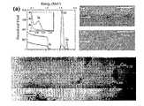
- FIG. 1shows: (a) RBS aligned (dotted line) and random (solid line) spectra of Si 0.20 Sn 0.08 Ge 0.72 epilayer and Sn 0.02 Ge 0.98 buffer layer showing a highly aligned heterostructure (Inset: magnified view of the Si peak indicating complete substitutionality of Si in the Sn—Ge lattice); (b) XTEM of the entire heterostructure; (c) Si/Sn 0.02 Ge 0.98 interface (indicated by arrow); and (d) Si 0.20 Sn 0.08 Ge 0.72 /Sn 0.02 Ge 0.98 interface;
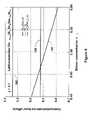
- FIG. 2shows reciprocal space maps showing the (224) reflections of Sn 0.02 Ge 0.98 buffer layer, Si 0.20 Ge 0.70 Sn 0.10 epilayer and Si substrate relative to the Si peak.
- the (004) peaksare shown in the inset.
- the corresponding in-plane lattice parametersare virtually identical.
- the epilayer peaklies on the line connecting the Si peak to the origin.
- the datashow that this line passes through the center of GeSn peak, consistent with fully relaxed GeSn grown on Si.
- the SiGeSn layerfalls directly below the SnGe buffer indicating that its in-plane lattice constant matches that of GeSn.
- the filmis thus fully strained with respect to the buffer layer;
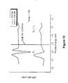
- FIG. 3shows silicon concentration in a SiGe alloy (x 2 ) versus Si concentration in a SiGeSn alloy (x 1 ) with 10% Sn;
- FIG. 4shows energy bands at a SiGeSn/SiGe interface.
- the lines 100correspond to the SiGe bands.
- the black linescorrespond to the SiGeSn bands.
- the zero of energyis at the top of the valence band in the SiGeSn alloy.
- the valence band offsetdepends only on y. Further, there is a substantial conduction band offset for x 1 ⁇ 0.6;
- FIG. 5shows the band gap of the SiGeSn/SiGe heterostructure shown in FIG. 4 ;
- FIG. 6shows band offsets at the SiGeSn/SiGe heterostructure shown in FIG. 4 .
- the lines 102are the conduction band offsets.
- the lower linecorresponds to the minimum band offset, the upper line to the offset between states with the same L-symmetry.
- the line 104is the valence band offset;
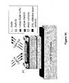
- FIG. 7shows a strain-free single quantum well structure with a band gap of 0.8 eV (1.55 microns) grown on a previously synthesized lattice matched Ge 0.78 Si 0.20 Sn 0.02 buffer layer;
- FIG. 9shows a strain-free multi-quantum well with a band gap of 0.8 eV (1.55 microns) grown on a Ge 1 ⁇ x Si x Sn 0.02 buffer layer;
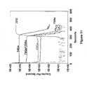
- FIG. 10shows absorption coefficients of bulk Ge and a Sn 0.02 Ge 0.98 film grown on Si
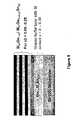
- FIG. 11shows the SIMS elemental profile of Ge 0.95 Sn 0.05 containing a highly uniform As concentration throughout the sample
- FIG. 12shows typical PR spectra obtained at 15K for GeSn alloys showing a shift of the direct band gap E 0 relative to that of pure Ge (the 4% Sn has a phase difference due to surface depletion);
- FIG. 13shows a simple demonstration of a modulator operating in transmission at 1.55 ⁇ m.
- the Si substrateis transparent at 1.55 ⁇ m;
- FIG. 14shows a reflective modulator based on Si—Sn—Ge/GeSi quantum wells.
- the quarter wave mirror stack in this casewill be replaced by a single layer of conductive and completely reflective ZrB 2 ;
- FIG. 15shows an XTEM interface image of an epitaxial Ge film grown on a ZrB 2 buffer layer
- FIG. 16shows an interface image showing epitaxial alignment of ZrB 2 with Si. Periodic defects at interface (shown by arrows) are due to the lattice mismatch.
- the filmsgrow strain-free with thickness of at least 1 ⁇ m. These films display smooth surface topologies and extremely low defect densities. While these films do show some defects, these defects are primarily Lomer edge dislocations that are concentrated at the Si interface with substantially no dislocation cores propagating to the film surface.
- a substantially defect-free surface for such an alloymay be achieved in films having a thickness of 20-25 nm.
- alloy systems described hereinalso address the thermal stability concerns described above.
- the thermal stability of alloy samples with a Sn content in the range of 2-5%is between 750° C. and 650° C., respectively. This temperature range is well within the temperature processing range of typically CMOS manufacturing processes.
- the optical properties of the materials disclosed hereinalso exhibit a well-defined Ge-like band structure and have a strong compositional dependence in the band gap energies.
- a systematic narrowing of the direct band gap E 0 and critical point energies with increasing Sn concentrationis observed (E 0 is reduced monotonically from 0.74 eV for Ge 0.98 Sn 0.02 to 0.41 eV for Ge 0.86 Sn 0.14 ).
- MBE filmsdiffer markedly from the materials disclosed here and the optical properties of conventional semiconductor alloys. 5b In MBE films and conventional semiconductor alloys, individual interband transitions are not observed, and the position of the band edges is obtained from fits that must incorporate transitions not found in pure Ge.
- the materials disclosed hererepresent a significant breakthrough from the point of view of achieving epitaxial growth of strain-free materials directly on Si.
- these alloy materialsdisplay a Ge-like band structure, which demonstrates that Ge 1 ⁇ x Sn x alloys are viable candidates for a variety of novel devices.
- Ellipsometry, and photoreflectance data taken on the disclosed materialsclosely resembles spectra for pure Ge. This data allows for the identification of optical transitions in the materials and demonstrates the much higher quality (e.g., device quality) of the disclosed materials as compared to MBE grown films.
- such materialsallow for highly efficient Rutherford back scattering (RBS) channeling by the Sn and the Ge. This material characteristic is important because it allow for the substitutionality of Sn in such alloys to be clearly demonstrated.
- RBSRutherford back scattering
- Si—Ge—Sn alloy systemsDevice-quality Si—Ge—Sn ternary materials that possess a variable and controllable range of compositions and exhibit lattice constants above and below that of bulk Ge 14,15 are also disclosed. These materials form more readily and exhibit even greater thermal stability than their Sn—Ge counterparts. Combined with the Sn x Ge 1 ⁇ x films disclosed herein, the new ternary system provides unprecedented flexibility for band gap and strain engineering in group IV alloys. Possible applications (aside from the photonic devices highlighted in the previous sections) include buffer layers for growth of relaxed SiGe alloys with high Ge content to be used in the modulator device structures described in this proposal and barrier layers for novel type I direct gap Ge quantum wells. 4
- Example ternaries Ge 1 ⁇ x ⁇ y Sn x Si y described hereinare grown on Si(100) using Ge 1 ⁇ x Sn x alloy buffer layers as illustrated by the RBS and TEM data shown in FIG. 1 .
- the crystal structure, elemental distribution and morphological properties of the heterostructuresare characterized by high-resolution TEM, including electron energy loss nanospectroscopy, x-ray diffraction and AFM.
- These techniquesdemonstrate growth of very high-quality epitaxial, uniform and highly aligned layers with atomically smooth surfaces and monocrystalline structures that have lattice constants close to that of Ge.
- RBS ion channelingshows that the constituent elements occupy random substitutional sites in the same average diamond cubic lattice and the Raman shifts are consistent with the lattice expansion produced by the Sn incorporation into SiGe tetrahedral sites.
- the structural and strain properties of these materialsare still relatively unknown and a multidisciplinary effort to evaluate these properties is in currently progress.
- the lattice constant of such materials as a function of composition (especially deviations from linearity) and their strain when grown on Simay be investigated by high resolution x-ray diffraction (XRD).
- FIG. 2illustrates an x-ray reciprocal space map data of a Si 0.20 Sn 0.10 Ge 0.70 /Sn 0.02 Ge 0.98 /Si(100) heterostructure.
- the data in FIG. 2indicate a fully strained SiGeSn epilayer with respect to the relaxed GeSn buffer layer.
- Related studieshave shown that tensile strained as well as relaxed SiGeSn films can be obtained on strain-free GeSn buffer layers. These results are significant because they demonstrate that strain engineering can be achieved in SiGeSn heterostructures and multilayers by tuning (adjusting) the lattice parameter of the GeSn buffer layer.
- a host of strained engineered optical and electronic devicesmay be designed based on this concept. 4 It is noted that the strain of such material systems is mechanically reliable up to at least 400-500° C. (where 400° C. is the growth temperature for the films).
- various combinations of concentrations in the Si—Ge—Sn alloy system to form strained-layer heterostructuresmay be achieved.
- Ge 1 ⁇ x ⁇ y Sn x Si y on Ge 1 ⁇ x Sn x bufferswhere the strain of the ternary can be tuned by adjusting the Si content in the film or the Sn content in the buffer may be produced.
- the growth of strained Ge films on Ge 1 ⁇ x Sn x buffersmay also be achieved.
- theorysuggests that tensile Ge layers will operate as direct bandgap materials when the Sn content in the buffer layer exceeds 10 at. %. 16,17
- Other technologically relevant systemsinclude the growth of strained Si on Si-rich Si y Ge 1 ⁇ y , where the quality of the Si y Ge 1 ⁇ y buffer is improved through incorporation of a small amount of Sn.
- ternary SiGeSn alloysas described herein provides for substantial flexibility for band gap and strain engineering in group-IV heterostructures.
- use of these materialsto design and grow interesting optical devices integrated with silicon such as simple modulators based on the Quantum Confined Stark Effect (QCSE) (which is essentially a shift in the energy levels of the structure and the resulting transition energies when an electric field is applied).
- QCSEQuantum Confined Stark Effect
- Studies of quantum well structures based on Si/SiGesuggest that such systems are not ideally suited for optical modulation applications due to their inherently small conduction band offsets. 18-23
- An additional complication of such systemsis that the Si/SiGe system has an indirect band gap.
- the first direct transitionis at much higher energies (for Si-rich alloys), so that the near band absorption coefficient is reduced relative to direct-gap group III-V systems.
- many multiple-quantum well periodsare needed to achieve the required on-off ratios, but this approach may then conflict with a desire to maintain the epitaxial strain.
- SiGeSn/SiGe systemsas disclosed herein address at least some of the difficulties mentioned above.
- the addition of Snallow for the design of substantially strain-free structures that can accommodate multi-quantum well systems with an arbitrary number of periods, and at the same time are likely to display much larger band offsets.
- the indirect and direct edgesare much closer in energy than in Si-rich SiGe alloys, so that there should be increased absorption due to oscillator strength “borrowing” induced by alloy fluctuations.
- FIG. 4illustrates these concepts.
- FIG. 4a graph that illustrates the electronic bands of Ge 1 ⁇ x 1 ⁇ y Si x 1 Sn y /Ge 1 ⁇ x 2 Si x 2 heterostructures for which the concentrations x 1 and x 2 are chosen so that the two components are lattice-matched are shown.
- the band lineupdepends on a number of parameters. For instance, one important such parameter is the dependence of the average valence band offset on Sn concentration.
- the data in FIG. 4is based on a theoretical model developed by Jaros, which matches well with experimentally known band offsets. 24
- a region of interestis the range of 0.4 ⁇ x 1 ⁇ 0.6. In this range, both holes and electrons are localized in the SiGe layer and there is a substantial conduction band offset.
- the band gap for those concentrationsis the difference between the CB_L_x 2 and the VB_x 2 band edges. This band gap covers the industry important 1.55 ⁇ m range and is shown in further detail in FIG. 5 .
- the valence band offsetis larger than 100 meV and the conduction band offset is larger than 100 meV over a significant range.
- the smallest conduction band offset shown in FIG. 6is between the L-type states on the SiGe side and the X-type states on the SiGeSn side.
- the effective barrier for electronsis more likely to be the difference between the L states on both sides of the heterojunction.
- This offsetis shown as the upper line 102 in FIG. 6 . As is shown in FIG. 6 , this offset is nearly 350 meV, which is very substantial. Based on this offset, it may be concluded that such a heterostructure will provide strong confinement of both electrons and holes.
- such structuresmay be further “tuned” using stress/strain.
- the band structuremay be further adjusted by changing the compositions in such a way that the added effect of strain leads to the desired band alignment.
- layers with lattice constants above and below the lattice constant of Gecan be grown using the techniques described herein, any sign of strain (positive or negative) is attainable.
- the effect of strain on the electronic bandshas been comprehended in the models discussed here. Therefore, calculations with strain as an extra “dimension” are very straightforward from these models.
- these principlesallow for the design of strain-compensated structures that are not substantially limited in total device length.
- Quantum wells based on a Ge 1 ⁇ x1 ⁇ y Si x1 Sn y /Ge 1 ⁇ x2 Si x2 systemmay be grown based on the theoretical models presented in the previous section.
- the Si concentration (x 1 ) of the Ge 1 ⁇ x1 ⁇ y Si x1 Sn y layer of the devicetargets the range of 40-60 at. % while the corresponding Si concentrations (x 2 ) of the Ge 1 ⁇ x2 Si x2 film are between 5-25 at. %, respectively.
- the matching bandgaps for the proposed heterostructureswill vary from 0.65 eV and 0.9 eV, respectively, based on the model illustrated in FIG. 5 .
- SQWssingle quantum wells
- MQW systemsmay be produced.
- An example SQW systemincludes a thin layer of Si 0.15 Ge 0.85 -Si 0.20 Ge 0.80 sandwiched between two thick layers of SiGeSn. Such a structure is illustrated in FIG. 7 . This material has a bandgap of 0.8 eV corresponding to a technologically important wavelength of operation for communication applications (1550 nm). Such material may be grown on lattice matched Si—Ge—Sn based buffer layers.
- FIG. 7illustrates such a material grown directly on Si (100). The structural morphological and crystallographic properties of the material were determined by high resolution x-ray diffraction, AFM and high resolution electron microscopy.
- FIG. 9illustrates an example MQW structure based on this approach.
- the starting composition of the buffer layeris essentially pure Sn—Ge with a composition close to Ge 0.98 Sn 0.02 at the substrate interface. Above the interface, the composition is graded via incorporation of Si (by adjusting the proportions of the reactant gases accordingly) to form a SiGeSn buffer layer with a lattice constant that is close to that of the Si x2 Ge 1 ⁇ x2 component of the device.
- Sn—Ge alloysto be used as buffer layers because they possess crystallographic, morphological and mechanical properties that make them uniquely suitable for use as templates on Si substrates. These alloys grow as uniform, substantially strain-free layers with essentially smooth and continuous surface morphologies (e.g., typical AFM rms values are 0.5-1.0 nm) and display extremely low concentrations of threading defects, particularly those that extend to the uppermost surface. In comparison, the quality of pure Ge films grown on Si by similar methods is typically much worse. In addition, such alloys are high compressibility (softer) solids as compared to either Si or SiGe and they can act as spacers that conform structurally and absorb the differential strain imposed by more rigid Si and Si—Ge layers.
- Sn—Ge buffer layersare not expected to absorb any significant amount of light emitted by heterostructures formed on such buffer layers. Based on IR measurements, the absorption of a common buffer layer with composition Ge 0.98 Sn 0.02 is approximately 10 4 cm ⁇ 1 in the energy range of 1.9 to 0.7 eV, which is illustrated in FIG. 10 . This indicates that a nominal thickness of 10-100 nm is essentially non-absorbing and clearly suitable for device application.
- GeSn buffer layersmay be grown directly on Si(100) using unique CVD procedures.
- the Ge 1 ⁇ x Si x component of the heterostructureis synthesized via reactions of appropriate amounts of the custom made and highly-reactive gaseous species H 2 Si(GeH 3 ) 2 and HSi(GeH 3 ) 3 with commercially available mixtures of Ge 2 H 6 (digermane) and H 2 .
- Deposition experiments involving the unimolecular dehydrogenation of H 2 Si(GeH 3 ) 2 directly on Si (100) via this approach using a gas source MBE reactor equipped with a low energy electron microscopehave shown that the entire deposition process may be monitored in situ in real time.
- Ge-rich Si—Ge films with variable concentration in the target range of Ge 67 Si 33 and thickness of 40-80 nmwere obtained between 480° C.-550° C. These materials displayed substantially completely smooth surface morphologies (rms 0.3-0.4 nm), low defect densities and were of superior quality to those with similar concentrations obtained by conventional CVD and/or MBE. These results indicate that such low temperature methods are especially applicable for growing the desired Ge 1 ⁇ x Si x component of the heterostructure.
- Ge 1 ⁇ x1 ⁇ y Si x1 Sn y layers of a heterostructure deviceare grown on a Ge 1 ⁇ x2 Si x2 layers using a synthesis method involving UHV-CVD reactions of specially prepared hydride precursors ⁇ i.e. SiH 3 GeH 3 or (SiH 3 ) 2 GeH 2 ⁇ with SnD 4 .
- the desired film composition and thicknessis controlled via appropriate precursor design, suitable concentrations of reactants and optimal growth conditions such as reactor pressure, temperature and flow rates.
- the hypothetical Ge 0.30 Si 0.60 Sn 0.10 compositionwill be formed by using a (SiH 3 ) 2 GeH 2 derivative as the source of Si and Ge. The entire Si 2 Ge concentration of two Si atoms and one Ge atom in the precursor is then incorporated in the film.
- High resolution TEMmay be used to evaluate he microstructural properties (heteroepitaxial character, layer thickness, topology and defect densities). Data from such evaluation is then used to adjust the growth conditions and ultimately produce material with desired crystal quality for device applications.
- the Si Ge and Sn concentration and layer thicknessis obtained by RBS. Complementary ion channeling experiments may be used to investigate the epitaxial alignment of the films and the substitutionality of the constituent elements in the structure.
- Strain as a function of buffer layer lattice dimensions, as well as other basic structural and morphological propertiesmay be evaluated by high-resolution x-ray diffraction and atomic force microscopy.
- High resolution x-ray measurementsincluding symmetric and asymmetric diffraction scans, rocking curves, reciprocal space maps, glancing incidence diffraction and reflectivity play a crucial role in the determination of key properties such as heteroepitaxial alignment, superlattice periodicity, lattice strain and relaxation, mismatch and composition, layer thickness and interface quality, etc.
- An x-ray diffractometer equipped with a hot stagewhich can reach temperatures up to 900° C. allows for investigation of the thermal stability of the layers, thermal expansion coefficients, and the strain relaxation of the alloys on Si.
- Hall measurementsmay be used to determine free carrier concentration, carrier polarity type and mobility as a function of temperature.
- P and N doping proceduresmay be developed as is described below.
- Doping of the Si—Ge—Sn AlloysThe need for doped layers in modulator devices, such as those disclosed herein, in combination with the disadvantages of current doping techniques demonstrates that alternative approaches for doping Si—Ge—Sn alloys in situ are desirable. For instance, Si and Si—Ge are currently doped with B using diborane, and with As by implantation methods, but there are limits to how much dopant can be incorporated into the structure using such techniques. For Si—Ge—Sn systems, there is also a risk of damaging the relatively “soft” structure using implantation processes. Accordingly, doping protocols that include in situ incorporation of the dopant atoms using custom prepared As, B, and P hydride precursors are employed to dope the structures disclosed herein.
- These compoundsare co-deposited with appropriate Si/Ge/Sn sources to from Sn—Ge or Si—Ge—Sn doped with the appropriate carrier type.
- appropriate Si/Ge/Sn sourcesto from Sn—Ge or Si—Ge—Sn doped with the appropriate carrier type.
- increases in the free carrier concentrationare achieved using such techniques by building precursors with direct Ge—As bonds such as As(GeH 3 ) 3 .
- This compoundhas been synthesized, as well as the P(GeH 3 ) 3 analog compound.
- These unique speciesare excellent molecular sources for low temperature, low cost, high efficiency doping applications that are conducted via simple, single-step processes.
- the compoundsare carbon-free inorganic hydrides and are designed to furnish a basic structural unit comprised of the dopant atom surrounded by three Ge atoms.
- SIMSlow energy secondary ion mass spectrometry
- Hall/FTIR ellipsometrymeasurements to determine carrier concentrations and effective masses.
- FIG. 11shows a typical SIMS profile illustrating highly uniform elemental distribution. These data are used to quantify the dopant content (implanted samples of known concentration are used as standards).
- XTEM and RBS analysisindicate good crystal quality of all Ge—Sn:As films.
- IR ellipsometryindicates that doping levels of ⁇ 5 ⁇ 10 19 /cm 3 have been achieved.
- Optical CharacterizationPossible optical characterization experimental techniques include photoluminescence (PL), inelastic light scattering, spectroscopic ellipsometry and photoreflectance (see FIG. 12 for a typical PR spectrum of materials described herein).
- PLmay be used to determine the system's band gap energy and to study the QCSE through the resulting shift in emission energies.
- Inelastic light scatteringmay be used to measure band offsets. It has been shown that inelastic light scattering is a highly sensitive method for the measurement of band offsets [See, J. Menéndez and A. Pinczuk, IEEE J. Quantum Elec. 24, 1698 (1988), which is incorporated by reference herein in its entirety].
- SiGeSn layers of various compositionsmay be grown for characterization with spectroscopic ellipsometry (from the infrared to the visible) and photoreflectance.
- a goal of such characterizationis to determine the compositional dependence of the optical transitions and properties relevant to our modeling efforts, including refractive index.
- Theoretical ModelingThe purpose of the theoretical modeling described herein is at least twofold: (i) to generate more realistic band offsets and (ii) to study the elastic properties of SiGeSn in detail. It is well known that density functional theory within the local-density-approximation makes very accurate predictions of ground-state properties in semiconductors. This includes lattice parameters, elastic constants, and the potential steps at heterojunctions, which determine band offsets. Corresponding structural work may be focused on the compositional dependence of lattice constants and elastic constants. The lattice constants and elastic constants are of interest because they determine the distribution of strain. Tetragonal distortion under biaxial strain depends on the ratio C 11 /C 12 of lattice constants. This ratio is about the same in Si and Ge, so that we can safely interpolate in the case of SiGe alloys. However, the deviation with Sn is larger, and so the compositional dependence of the C 11 /C 12 ratio requires some theoretical modeling.
- Ionic pseudopotentialsare used to eliminate the core electrons from the physical description.
- the remaining valence electron densityis expanded in a plane-wave basis, and density functional theory is used to obtain the electronic structure.
- Atomic forces and cellular stresses obtained from the resulting wavefunctionsare then minimized to yield a prediction for the ground state atomic/ionic configuration of a target material.
- the electronic band-structureis also available as a function of composition at every stage of the calculation and allows us to compute local fields, band-offsets, chemical potentials, polarizability tensors, elastic constants, work functions, space charge and many other key properties of a semiconductor system.
- Free surfaces and interfacesare of interest since they play a prominent role in device design.
- Band offsets and Schottky barriersare computed from spatial moments of the induced charge density at the interface between two materials. The potential line-up obtained in this way is sensitive to the chemical and structural properties of the interface.
- the valence band offsetis calculated by summing the potential offset and the valence-band edge difference between the two interface materials. The latter are obtained from conventional bulk band-structure calculations. Using this procedure the effect of bulk and interface strain effects on the valence band offset can be estimated and compared with experimental data as part of a comprehensive band-engineering/materials design approach. The effects of compositional variation on both the valence and conduction band offsets can thus be systematically and efficiently explored.
- the structures described hereinmay be redesigned to achieve the desired large valence and conduction band offsets. If needed, strain engineering may be implemented to manipulate the offsets.
- growth of the MQW structurese.g., as are required for modulators
- FIG. 13A schematic illustrating such a modulator structure is shown in FIG. 13 . The modulation properties of such a quantum well stacks may be evaluated using photocurrent spectroscopy.
- the disclosed QCSE modulatoroperates via electroabsorption. This leads to a modulation of the light intensity.
- phase modulationproduced by electric-field induced changes in the index of refraction. This is commonly known as electrorefraction.
- the phase modulationcan be converted into intensity modulations by fabricating interferometric devices using waveguides.
- Our proposed SiGeSn/SiGe quantum well structuresare very attractive from this perspective due to their high index of refraction.
- the refractive indices of the buffer and quantum wellsare expected to be significantly larger than 3.5 (e.g., a measured refractive index for a Sn 0.02 Ge 0.98 film at the approximate energy of the indirect gap is 4.2), so that the silicon substrate will provide bottom confinement. Air or low temperature oxide (LTO) may provide top confinement.
- LTOlow temperature oxide
- the fabrication of waveguidesappears to be very straightforward.
- the electromodulation of such structuresis not sensitive to the details of the near band gap band structure (the index of refraction depends on the entire band structure), so that the strength of the electrorefraction effect in the alloys described herein should be comparable to the average for bulk elemental semiconductors.
- One concern for these types of structuresis possible losses due to sidewall roughness.
- a simple and efficient approach for incorporating a reflective modulator structure with a Si substrateincludes growth of ZrB 2 thin epitaxial layers directly on the Si.
- This ZrB 2 materialwill serve as the template for the subsequent growth of the appropriate Ge—Sn or SiGeSn buffer layers upon which the modulator structure will be built.
- the misfit at the interfaceis taken up by a pure edge-type dislocation from the insertion of extra ⁇ 1100 ⁇ lattice planes along the [ 1120 ] direction. No threading dislocations propagating in a direction normal to the substrate were observed.
- the ZrB 2 layer on Si(111)would provide a near lattice-matched template for subsequent growth of epitaxial nitrides (GaN and InGaN). 26
- ZrB 2would serve as a reflecting intermediate layer, which prevents any substantial loss of emission intensity from the light emitting overlayer into the absorbing Si substrate, thus allowing for integration of nitride electronics with conventional Si electronics. 27
- the epitaxial alignment between Si and ZrB 2suggests that growth of Ge and SnGe on ZrB 2 might be possible. The successful growth of these materials on reflecting surfaces would have important applications in IR devices such as the reflective modulator structure illustrated in FIG. 14 .
- FIGS. 15 and 16The result of pure Ge grown on a ZrB 2 /Si heterostructure via deposition of digermane (Ge 2 H 6 ) at 450° C. is shown in FIGS. 15 and 16 .
- FIG. 15the result of XTEM studies are shown that reveal highly coherent Ge films with near perfect epitaxial alignment with the ZrB 2 buffer layer. This method may then be extended to grow GeSn and SiGeSn films on ZrB 2 . These materials may then be used as buffer layers for the subsequent growth of a Ge 1 ⁇ x1 ⁇ y Si x1 Sn y /Ge 1 ⁇ x2 Si x2 quantum well structure, such as a modulator device with a wavelength preferably around 1.55 ⁇ m (e.g., the structure shown in FIG.
Landscapes
- Engineering & Computer Science (AREA)
- Physics & Mathematics (AREA)
- General Physics & Mathematics (AREA)
- Microelectronics & Electronic Packaging (AREA)
- Manufacturing & Machinery (AREA)
- Computer Hardware Design (AREA)
- Power Engineering (AREA)
- Condensed Matter Physics & Semiconductors (AREA)
- Chemical & Material Sciences (AREA)
- Optics & Photonics (AREA)
- Nonlinear Science (AREA)
- Nanotechnology (AREA)
- Life Sciences & Earth Sciences (AREA)
- Crystallography & Structural Chemistry (AREA)
- Biophysics (AREA)
- Materials Engineering (AREA)
- Optical Modulation, Optical Deflection, Nonlinear Optics, Optical Demodulation, Optical Logic Elements (AREA)
Abstract
Description
- It has been known for some time, at least on theoretical grounds, that high quality Si—Ge—Sn alloy systems will possess very interesting material properties, especially when implemented in infrared (IR) devices (such as detectors, sensors or modulators). This knowledge has prompted extensive experimental efforts to develop techniques to manufacture (e.g., grow) such alloy compounds. However, historically, the resulting quality of such alloy materials has not been sufficiently high (e.g., due to lattice mismatch between materials, among other factors) so as to allow for effective use of such alloys in device applications (e.g., in infrared devices). Therefore, alternative methods for manufacturing such Si—Ge—Sn alloy systems are desirable.
- The foregoing discussion of the related art and limitations related therewith is intended to be illustrative and not exclusive. Other limitations of the related art will become apparent to those of skill in the art upon a reading of the specification and a study of the drawings.
- The following embodiments and aspects thereof are described and illustrated in conjunction with systems, tools and methods which are given by way of example and meant to be illustrative, not limiting in scope. In various embodiments, one or more of the above-described problems have been reduced or eliminated, while other embodiments are directed to other improvements.
- High quality Sn—Ge and Si—Ge—Sn alloys (alloy systems) and methods for manufacturing such alloys are disclosed. Such alloys are of sufficient quality so as to allow for their use in device applications. The manufacture of such alloys is achieved through chemical vapor deposition (CVD) techniques that have been developed for forming such materials, and are also disclosed herein.
- The ability to form (manufacture) such device quality alloys has significant industry value for a number of reasons. For example, SnxGe1−xalloys have been predicted to undergo a transition from indirect-to direct-gap semiconductors. Therefore, the availability of such alloy materials may ultimately allow for a direct-gap semiconductor to be fully integrated with Si technology.1,2
- Further, such device-quality SnxGe1−xlayers of arbitrary thickness may be deposited directly on Si and these alloy layers may be used as “virtual substrates” or “buffer layers” for the growth of Ge1−x−ySixSnyternary analogs.3The fabrication of Ge1−x−ySixSnymakes it possible (using such a buffer alloy layer) to decouple strain and band gap engineering to achieve unique device structures that allow for the production of photonic devices based entirely on group IV materials. Such applications may cover a wide range of operating wavelengths in the IR range and include strain-engineered direct gap heterodiodes and multi-quantum well lasers; photodetectors; emitters and modulators grown on Sn1−xGexand Ge1−x−ySixSnybuffered Si.4
- In an example embodiment, alloy systems that are specifically designed to display quantum confinement Stark effects (QCSE) are implemented. These materials can be used to fabricate new modulator devices, such as are disclosed herein.
- Materials that display such QCSE are disclosed herein. These materials include Si—Ge—Sn semiconductors that are manufactured using the methods that are disclosed herein. These materials may be used to fabricate optical devices that utilize indirect transitions to obtain modulation of the absorption and index of refraction at IR wavelengths of technological interest.
- In order to evaluate the potential application of alloy materials that are disclosed herein, experiments on growth characterization, properties measurement and performance evaluation of materials which include single quantum well (SQW) Ge1−x1−ySix1Sny/Ge1−x2Six2heterostructures grown fully strained or strain-free on Si(100) via Sn1−xGexbuffer layers may be performed. The alloy materials included in these structures may be deposited using CVD techniques that include the use of specially designed molecular precursors. Such materials also will display strong QCSE (e.g., a shift in exciton absorption peaks in a quantum well structure when an electric field is applied). Such SQWs may then be utilized as building blocks to fabricate multi quantum well (MQW) modulator structures with band gaps covering the 1.4-1.9 μm range, which is of value to industry.
- An example free space modulator structure operating in transmission at 1.55 μm that predominately relies on electro-absorption (EA) is disclosed herein. Further, a reflective version of such an EA modulator is also described. For the reflective EA modulator, in addition to the conventional multi-layer dielectric stack mirror, the structure is fabricated, in part, by forming a reflective modulator device based on the above described MQWs and a single layer of conductive and fully reflective ZrB2.
- Waveguide structures that may be used as the basis of optical modulators operating via electro-refraction are also described. Such waveguide structures may be formed using the same MQW systems discussed above. Waveguide-based electro-absorption modulator devices are also discussed herein.
- The devices described herein take advantage of expertise that has been gained in the area of materials growth, as is disclosed herein. This expertise includes processing techniques and determination of the material property of Sn lowering the direct gap in certain materials so as to allow for the design and fabrication of devices that utilize absorptions based on direct transitions in single-quantum wells (e.g., positive-intrinsic-negative (PIN) photodetectors) that may operate between 1.55 μm and 5.00 μm.
- Using the techniques disclosed herein, a semiconductor structure including a single quantum well Ge1−x1−ySix1Sny/Ge1−x2Six2heterostructure grown strain-free on Si(100) with a Sn1−xGexbuffer layer may be achieved.
- Example embodiments are illustrated in referenced figures of the drawings. It is intended that the embodiments and figures disclosed herein are to be considered illustrative rather than restrictive.
FIG. 1 shows: (a) RBS aligned (dotted line) and random (solid line) spectra of Si0.20Sn0.08Ge0.72epilayer and Sn0.02Ge0.98buffer layer showing a highly aligned heterostructure (Inset: magnified view of the Si peak indicating complete substitutionality of Si in the Sn—Ge lattice); (b) XTEM of the entire heterostructure; (c) Si/Sn0.02Ge0.98interface (indicated by arrow); and (d) Si0.20Sn0.08Ge0.72/Sn0.02Ge0.98interface;FIG. 2 shows reciprocal space maps showing the (224) reflections of Sn0.02Ge0.98buffer layer, Si0.20Ge0.70Sn0.10epilayer and Si substrate relative to the Si peak. The (004) peaks are shown in the inset. The data is given for cSiGeSn=5.728 Å and cGeSn=5.681 Å. The corresponding in-plane lattice parameters are virtually identical. For full relaxation, the epilayer peak lies on the line connecting the Si peak to the origin. The data show that this line passes through the center of GeSn peak, consistent with fully relaxed GeSn grown on Si. Note that the SiGeSn layer falls directly below the SnGe buffer indicating that its in-plane lattice constant matches that of GeSn. The film is thus fully strained with respect to the buffer layer;FIG. 3 shows silicon concentration in a SiGe alloy (x2) versus Si concentration in a SiGeSn alloy (x1) with 10% Sn;FIG. 4 shows energy bands at a SiGeSn/SiGe interface. Thelines 100 correspond to the SiGe bands. The black lines correspond to the SiGeSn bands. The zero of energy is at the top of the valence band in the SiGeSn alloy. The Sn concentration is y=0.1. In this model, the valence band offset depends only on y. Further, there is a substantial conduction band offset for x1<0.6;FIG. 5 shows the band gap of the SiGeSn/SiGe heterostructure shown inFIG. 4 ;FIG. 6 shows band offsets at the SiGeSn/SiGe heterostructure shown inFIG. 4 . Thelines 102 are the conduction band offsets. The lower line corresponds to the minimum band offset, the upper line to the offset between states with the same L-symmetry. Theline 104 is the valence band offset;FIG. 7 shows a strain-free single quantum well structure with a band gap of 0.8 eV (1.55 microns) grown on a previously synthesized lattice matched Ge0.78Si0.20Sn0.02buffer layer;FIG. 8 shows: (a) XTEM micrograph and SAED of Si(100)/Ge0.97Sn0.03/Ge0.78Si0.20Sn0.02showing smooth, continuous surface morphology and low defect densities. The total film thickness is 220 nm; (b) high resolution XTEM image of the Ge0.97Sn0.03/Ge0.78Si0.20Sn0.02interface indicating perfect epitaxial alignment; (c) AFM image showing smooth surface topology (RMS=1 nm). The lattice parameter of the top layer (0.562 nm) is identical to that of the quantum well structure shown inFIG. 7 indicating that this film may be an effective buffer layer for the materials disclosed herein;FIG. 9 shows a strain-free multi-quantum well with a band gap of 0.8 eV (1.55 microns) grown on a Ge1−xSixSn0.02buffer layer;FIG. 10 shows absorption coefficients of bulk Ge and a Sn0.02Ge0.98film grown on Si;FIG. 11 shows the SIMS elemental profile of Ge0.95Sn0.05containing a highly uniform As concentration throughout the sample;FIG. 12 shows typical PR spectra obtained at 15K for GeSn alloys showing a shift of the direct band gap E0relative to that of pure Ge (the 4% Sn has a phase difference due to surface depletion);FIG. 13 shows a simple demonstration of a modulator operating in transmission at 1.55 μm. The Si substrate is transparent at 1.55 μm;FIG. 14 shows a reflective modulator based on Si—Sn—Ge/GeSi quantum wells. The quarter wave mirror stack in this case will be replaced by a single layer of conductive and completely reflective ZrB2;FIG. 15 shows an XTEM interface image of an epitaxial Ge film grown on a ZrB2buffer layer; andFIG. 16 shows an interface image showing epitaxial alignment of ZrB2with Si. Periodic defects at interface (shown by arrows) are due to the lattice mismatch.- Prior Sn—Ge alloy systems: The growth of Ge1−xSnxalloys has been hampered by the enormous lattice mismatch (15%) between Ge and α-Sn as well as by the instability of the cubic α-Sn structure above 13° C. As a result, such alloy systems have been highly metastable and, therefore, not amenable to being produced in bulk form. Nevertheless, significant efforts have been devoted to growing SnxGe1−xfilms by molecular beam Epitaxy (MBE).5a,bHowever, such approaches also have certain drawbacks. For instance, one problem encountered with MBE techniques is the propensity of the Sn to segregate towards the film surface. Another problem is the low thermal stability and crystal quality of MBE grown materials.
- These drawbacks are addressed by the CVD techniques described herein. These CVD techniques allow for the production of device-quality single-crystal, SnxGe1−xalloys (with x=0.02-0.2) that may be grown directly on Si(100).6-10The films grow strain-free with thickness of at least 1 μm. These films display smooth surface topologies and extremely low defect densities. While these films do show some defects, these defects are primarily Lomer edge dislocations that are concentrated at the Si interface with substantially no dislocation cores propagating to the film surface. Using the approaches described herein, a substantially defect-free surface for such an alloy may be achieved in films having a thickness of 20-25 nm.
- Furthermore, alloy systems described herein also address the thermal stability concerns described above. For example, the thermal stability of alloy samples with a Sn content in the range of 2-5% is between 750° C. and 650° C., respectively. This temperature range is well within the temperature processing range of typically CMOS manufacturing processes.
- The optical properties of the materials disclosed herein also exhibit a well-defined Ge-like band structure and have a strong compositional dependence in the band gap energies. A systematic narrowing of the direct band gap E0and critical point energies with increasing Sn concentration is observed (E0is reduced monotonically from 0.74 eV for Ge0.98Sn0.02to 0.41 eV for Ge0.86Sn0.14).11-13
- The optical properties of MBE films (as discussed above) differ markedly from the materials disclosed here and the optical properties of conventional semiconductor alloys.5bIn MBE films and conventional semiconductor alloys, individual interband transitions are not observed, and the position of the band edges is obtained from fits that must incorporate transitions not found in pure Ge.
- In contrast, the materials disclosed here (e.g., GeSn alloys) represent a significant breakthrough from the point of view of achieving epitaxial growth of strain-free materials directly on Si. Unlike other groups, these alloy materials display a Ge-like band structure, which demonstrates that Ge1−xSnxalloys are viable candidates for a variety of novel devices. Ellipsometry, and photoreflectance data taken on the disclosed materials closely resembles spectra for pure Ge. This data allows for the identification of optical transitions in the materials and demonstrates the much higher quality (e.g., device quality) of the disclosed materials as compared to MBE grown films. Furthermore, such materials allow for highly efficient Rutherford back scattering (RBS) channeling by the Sn and the Ge. This material characteristic is important because it allow for the substitutionality of Sn in such alloys to be clearly demonstrated.
- Si—Ge—Sn alloy systems: Device-quality Si—Ge—Sn ternary materials that possess a variable and controllable range of compositions and exhibit lattice constants above and below that of bulk Ge14,15are also disclosed. These materials form more readily and exhibit even greater thermal stability than their Sn—Ge counterparts. Combined with the SnxGe1−xfilms disclosed herein, the new ternary system provides unprecedented flexibility for band gap and strain engineering in group IV alloys. Possible applications (aside from the photonic devices highlighted in the previous sections) include buffer layers for growth of relaxed SiGe alloys with high Ge content to be used in the modulator device structures described in this proposal and barrier layers for novel type I direct gap Ge quantum wells.4
- Example ternaries Ge1−x−ySnxSiydescribed herein are grown on Si(100) using Ge1−xSnxalloy buffer layers as illustrated by the RBS and TEM data shown in
FIG. 1 . InFIG. 1 , the crystal structure, elemental distribution and morphological properties of the heterostructures are characterized by high-resolution TEM, including electron energy loss nanospectroscopy, x-ray diffraction and AFM. These techniques demonstrate growth of very high-quality epitaxial, uniform and highly aligned layers with atomically smooth surfaces and monocrystalline structures that have lattice constants close to that of Ge. RBS ion channeling shows that the constituent elements occupy random substitutional sites in the same average diamond cubic lattice and the Raman shifts are consistent with the lattice expansion produced by the Sn incorporation into SiGe tetrahedral sites. - The structural and strain properties of these materials are still relatively unknown and a multidisciplinary effort to evaluate these properties is in currently progress. The lattice constant of such materials as a function of composition (especially deviations from linearity) and their strain when grown on Si may be investigated by high resolution x-ray diffraction (XRD).
FIG. 2 illustrates an x-ray reciprocal space map data of a Si0.20Sn0.10Ge0.70/Sn0.02Ge0.98/Si(100) heterostructure. The data inFIG. 2 indicate a fully strained SiGeSn epilayer with respect to the relaxed GeSn buffer layer. Related studies have shown that tensile strained as well as relaxed SiGeSn films can be obtained on strain-free GeSn buffer layers. These results are significant because they demonstrate that strain engineering can be achieved in SiGeSn heterostructures and multilayers by tuning (adjusting) the lattice parameter of the GeSn buffer layer. A host of strained engineered optical and electronic devices may be designed based on this concept.4It is noted that the strain of such material systems is mechanically reliable up to at least 400-500° C. (where 400° C. is the growth temperature for the films).- Using the methods and materials described herein, various combinations of concentrations in the Si—Ge—Sn alloy system to form strained-layer heterostructures may be achieved. For instance, Ge1−x−ySnxSiyon Ge1−xSnxbuffers, where the strain of the ternary can be tuned by adjusting the Si content in the film or the Sn content in the buffer may be produced. Further, the growth of strained Ge films on Ge1−xSnxbuffers may also be achieved. As was noted above, theory suggests that tensile Ge layers will operate as direct bandgap materials when the Sn content in the buffer layer exceeds 10 at. %.16,17Other technologically relevant systems include the growth of strained Si on Si-rich SiyGe1−y, where the quality of the SiyGe1−ybuffer is improved through incorporation of a small amount of Sn.
- Strain Free, Lattice Matched, Ge1−x1−ySix1Sny/Ge1−x2Six2Heterostructures on Si(100) for QCSE Applications
- The availability of ternary SiGeSn alloys as described herein provides for substantial flexibility for band gap and strain engineering in group-IV heterostructures. As is described herein, use of these materials to design and grow interesting optical devices integrated with silicon such as simple modulators based on the Quantum Confined Stark Effect (QCSE) (which is essentially a shift in the energy levels of the structure and the resulting transition energies when an electric field is applied). Studies of quantum well structures based on Si/SiGe suggest that such systems are not ideally suited for optical modulation applications due to their inherently small conduction band offsets.18-23An additional complication of such systems is that the Si/SiGe system has an indirect band gap. Therefore, the first direct transition is at much higher energies (for Si-rich alloys), so that the near band absorption coefficient is reduced relative to direct-gap group III-V systems. Thus, many multiple-quantum well periods are needed to achieve the required on-off ratios, but this approach may then conflict with a desire to maintain the epitaxial strain.24
- SiGeSn/SiGe systems as disclosed herein address at least some of the difficulties mentioned above. For instance, the addition of Sn allow for the design of substantially strain-free structures that can accommodate multi-quantum well systems with an arbitrary number of periods, and at the same time are likely to display much larger band offsets. Moreover, while such systems are still indirect gap materials, the indirect and direct edges are much closer in energy than in Si-rich SiGe alloys, so that there should be increased absorption due to oscillator strength “borrowing” induced by alloy fluctuations.
FIG. 4 illustrates these concepts. - In
FIG. 4 , a graph that illustrates the electronic bands of Ge1−x1 −ySix1 Sny/Ge1−x2 Six2 heterostructures for which the concentrations x1and x2are chosen so that the two components are lattice-matched are shown. Using Vegard's law (which is known to those working in this area), the resulting concentrations are shown inFIG. 3 for the case of y=0.1. All subsequent calculations presented here are based on this fixed Sn concentration, which is readily attainable. Notice that for about 40% Si concentration and 10% Sn concentration, the SiGeSn layer is very close to being lattice-matched with pure Ge. As demonstrated byFIG. 4 , the band lineup depends on a number of parameters. For instance, one important such parameter is the dependence of the average valence band offset on Sn concentration. The data inFIG. 4 is based on a theoretical model developed by Jaros, which matches well with experimentally known band offsets.24 - In
FIG. 4 , a region of interest is the range of 0.4<x1<0.6. In this range, both holes and electrons are localized in the SiGe layer and there is a substantial conduction band offset. The band gap for those concentrations is the difference between the CB_L_x2 and the VB_x2 band edges. This band gap covers the industry important 1.55 μm range and is shown in further detail inFIG. 5 . - Data shows that relaxed Ge1−x
1 −ySix1 Sny/Ge1−x2 Six2 is type-I, with both electrons and holes confined in the Ge1−x2 Six2 layers. The conduction band offsets are much larger than in the Si/SiGe system, so that the heterostructures disclosed herein are good candidates for the observation of the QCSE. This conclusion is apparent fromFIG. 4 and is displayed in more detail inFIG. 6 . - As shown in
FIG. 6 , the valence band offset is larger than 100 meV and the conduction band offset is larger than 100 meV over a significant range. Moreover, the smallest conduction band offset shown inFIG. 6 is between the L-type states on the SiGe side and the X-type states on the SiGeSn side. However, the effective barrier for electrons is more likely to be the difference between the L states on both sides of the heterojunction. This offset is shown as theupper line 102 inFIG. 6 . As is shown inFIG. 6 , this offset is nearly 350 meV, which is very substantial. Based on this offset, it may be concluded that such a heterostructure will provide strong confinement of both electrons and holes. - In the event that the band lineup of such structures is not suitable for a specific application, such structures may be further “tuned” using stress/strain. For instance, the band structure may be further adjusted by changing the compositions in such a way that the added effect of strain leads to the desired band alignment. Because layers with lattice constants above and below the lattice constant of Ge can be grown using the techniques described herein, any sign of strain (positive or negative) is attainable. The effect of strain on the electronic bands has been comprehended in the models discussed here. Therefore, calculations with strain as an extra “dimension” are very straightforward from these models. Moreover, these principles allow for the design of strain-compensated structures that are not substantially limited in total device length.
- Quantum wells based on a Ge1−x1−ySix1Sny/Ge1−x2Six2system may be grown based on the theoretical models presented in the previous section. In one embodiment of such a quantum well, the Si concentration (x1) of the Ge1−x1−ySix1Snylayer of the device targets the range of 40-60 at. % while the corresponding Si concentrations (x2) of the Ge1−x2Six2film are between 5-25 at. %, respectively. The matching bandgaps for the proposed heterostructures will vary from 0.65 eV and 0.9 eV, respectively, based on the model illustrated in
FIG. 5 . - Initially, single quantum wells (SQWs) based on selected lattice matched structures discussed above may be grown. Growth of these SQWs may then be followed by the growth of multiple-quantum well structures, as are described below. Example, simple SQW structures are useful as an initial demonstration of the QCSE using photoluminescence, and for the measurement of band offsets using inelastic light scattering. With information collected from experiments on such SQW structures, modification to structure design can be made and MQW systems may be produced. An example SQW system includes a thin layer of Si0.15Ge0.85-Si0.20Ge0.80sandwiched between two thick layers of SiGeSn. Such a structure is illustrated in
FIG. 7 . This material has a bandgap of 0.8 eV corresponding to a technologically important wavelength of operation for communication applications (1550 nm). Such material may be grown on lattice matched Si—Ge—Sn based buffer layers. - Various approaches for preparation of buffer layers may be used. One such approach is based on lattice-matched templates, such as with a composition Sn0.03Ge0.97/Ge0.78Si0.20Sn0.02, as is shown schematically in
FIG. 7 .FIG. 8 illustrates such a material grown directly on Si (100). The structural morphological and crystallographic properties of the material were determined by high resolution x-ray diffraction, AFM and high resolution electron microscopy. The data indicate that this material is suitable as a template for the growth of a Ge0.40Si0.50Sn0.10/Ge0.85Si0.15device particularly since the experimentally determined lattice parameter of the Ge0.78Si0.20Sn0.02top layer of the template equals that of the device as determined by Vegard's Law. - Another buffer-layer approach is based on a graded Ge1−xSixSn0.02layer grown on Si(100), followed by in situ CVD growth of the Ge1−x1−ySix1Sny/Ge1−x2Six2overlayers.
FIG. 9 illustrates an example MQW structure based on this approach. The starting composition of the buffer layer is essentially pure Sn—Ge with a composition close to Ge0.98Sn0.02at the substrate interface. Above the interface, the composition is graded via incorporation of Si (by adjusting the proportions of the reactant gases accordingly) to form a SiGeSn buffer layer with a lattice constant that is close to that of the Six2Ge1−x2component of the device. - We have chosen the Sn—Ge alloys to be used as buffer layers because they possess crystallographic, morphological and mechanical properties that make them uniquely suitable for use as templates on Si substrates. These alloys grow as uniform, substantially strain-free layers with essentially smooth and continuous surface morphologies (e.g., typical AFM rms values are 0.5-1.0 nm) and display extremely low concentrations of threading defects, particularly those that extend to the uppermost surface. In comparison, the quality of pure Ge films grown on Si by similar methods is typically much worse. In addition, such alloys are high compressibility (softer) solids as compared to either Si or SiGe and they can act as spacers that conform structurally and absorb the differential strain imposed by more rigid Si and Si—Ge layers. Another potential advantage of Sn—Ge buffer layers is that such layers are not expected to absorb any significant amount of light emitted by heterostructures formed on such buffer layers. Based on IR measurements, the absorption of a common buffer layer with composition Ge0.98Sn0.02is approximately 104cm−1in the energy range of 1.9 to 0.7 eV, which is illustrated in
FIG. 10 . This indicates that a nominal thickness of 10-100 nm is essentially non-absorbing and clearly suitable for device application. - Growth Strategies: GeSn buffer layers may be grown directly on Si(100) using unique CVD procedures. The Ge1−xSixcomponent of the heterostructure is synthesized via reactions of appropriate amounts of the custom made and highly-reactive gaseous species H2Si(GeH3)2and HSi(GeH3)3with commercially available mixtures of Ge2H6(digermane) and H2. Deposition experiments involving the unimolecular dehydrogenation of H2Si(GeH3)2directly on Si (100) via this approach using a gas source MBE reactor equipped with a low energy electron microscope have shown that the entire deposition process may be monitored in situ in real time. Ge-rich Si—Ge films with variable concentration in the target range of Ge67Si33and thickness of 40-80 nm were obtained between 480° C.-550° C. These materials displayed substantially completely smooth surface morphologies (rms 0.3-0.4 nm), low defect densities and were of superior quality to those with similar concentrations obtained by conventional CVD and/or MBE. These results indicate that such low temperature methods are especially applicable for growing the desired Ge1−xSixcomponent of the heterostructure.
- In an example embodiment, Ge1−x1−ySix1Snylayers of a heterostructure device are grown on a Ge1−x2Six2layers using a synthesis method involving UHV-CVD reactions of specially prepared hydride precursors {i.e. SiH3GeH3or (SiH3)2GeH2} with SnD4. The desired film composition and thickness is controlled via appropriate precursor design, suitable concentrations of reactants and optimal growth conditions such as reactor pressure, temperature and flow rates. For example, the hypothetical Ge0.30Si0.60Sn0.10composition will be formed by using a (SiH3)2GeH2derivative as the source of Si and Ge. The entire Si2Ge concentration of two Si atoms and one Ge atom in the precursor is then incorporated in the film.
- Characterization: High resolution TEM may be used to evaluate he microstructural properties (heteroepitaxial character, layer thickness, topology and defect densities). Data from such evaluation is then used to adjust the growth conditions and ultimately produce material with desired crystal quality for device applications. The Si Ge and Sn concentration and layer thickness is obtained by RBS. Complementary ion channeling experiments may be used to investigate the epitaxial alignment of the films and the substitutionality of the constituent elements in the structure.
- Strain as a function of buffer layer lattice dimensions, as well as other basic structural and morphological properties may be evaluated by high-resolution x-ray diffraction and atomic force microscopy. High resolution x-ray measurements including symmetric and asymmetric diffraction scans, rocking curves, reciprocal space maps, glancing incidence diffraction and reflectivity play a crucial role in the determination of key properties such as heteroepitaxial alignment, superlattice periodicity, lattice strain and relaxation, mismatch and composition, layer thickness and interface quality, etc. An x-ray diffractometer equipped with a hot stage which can reach temperatures up to 900° C. allows for investigation of the thermal stability of the layers, thermal expansion coefficients, and the strain relaxation of the alloys on Si.
- Hall measurements may be used to determine free carrier concentration, carrier polarity type and mobility as a function of temperature. P and N doping procedures may be developed as is described below.
- Doping of the Si—Ge—Sn Alloys: The need for doped layers in modulator devices, such as those disclosed herein, in combination with the disadvantages of current doping techniques demonstrates that alternative approaches for doping Si—Ge—Sn alloys in situ are desirable. For instance, Si and Si—Ge are currently doped with B using diborane, and with As by implantation methods, but there are limits to how much dopant can be incorporated into the structure using such techniques. For Si—Ge—Sn systems, there is also a risk of damaging the relatively “soft” structure using implantation processes. Accordingly, doping protocols that include in situ incorporation of the dopant atoms using custom prepared As, B, and P hydride precursors are employed to dope the structures disclosed herein. These compounds are co-deposited with appropriate Si/Ge/Sn sources to from Sn—Ge or Si—Ge—Sn doped with the appropriate carrier type. In the case of As, increases in the free carrier concentration are achieved using such techniques by building precursors with direct Ge—As bonds such as As(GeH3)3. This compound has been synthesized, as well as the P(GeH3)3analog compound. These unique species are excellent molecular sources for low temperature, low cost, high efficiency doping applications that are conducted via simple, single-step processes. The compounds are carbon-free inorganic hydrides and are designed to furnish a basic structural unit comprised of the dopant atom surrounded by three Ge atoms. This arrangement produces homogeneous, substitution of dopant atoms at high concentrations without clustering or segregation. We use low energy secondary ion mass spectrometry (SIMS) to determine the As elemental profile and Hall/FTIR ellipsometry measurements to determine carrier concentrations and effective masses.
FIG. 11 shows a typical SIMS profile illustrating highly uniform elemental distribution. These data are used to quantify the dopant content (implanted samples of known concentration are used as standards). XTEM and RBS analysis indicate good crystal quality of all Ge—Sn:As films. IR ellipsometry indicates that doping levels of ˜5×10¹⁹/cm3have been achieved. - Optical Characterization: Possible optical characterization experimental techniques include photoluminescence (PL), inelastic light scattering, spectroscopic ellipsometry and photoreflectance (see
FIG. 12 for a typical PR spectrum of materials described herein). PL may be used to determine the system's band gap energy and to study the QCSE through the resulting shift in emission energies. Inelastic light scattering may be used to measure band offsets. It has been shown that inelastic light scattering is a highly sensitive method for the measurement of band offsets [See, J. Menéndez and A. Pinczuk, IEEE J. Quantum Elec. 24, 1698 (1988), which is incorporated by reference herein in its entirety]. This method has historically not been applied to Si/SiGe quantum well systems because it cannot be used if the lowest conduction band edge is of X-type, as is the case in SiGe alloys with high Si concentration. However, in the material (alloy) systems disclosed herein the lowest conduction band edge is generally at the L-point of the Brillouin zone. This arrangement is desirable for light scattering, because the scattering cross section can be resonantly enhanced by working in resonance with the E1gap of the system. Moreover, the light scattering experiments are performed with visible laser excitation whereas photoluminescence occurs in the infrared range, so that there is essentially no overlap that could obscure the measurements. - SiGeSn layers of various compositions may be grown for characterization with spectroscopic ellipsometry (from the infrared to the visible) and photoreflectance. A goal of such characterization is to determine the compositional dependence of the optical transitions and properties relevant to our modeling efforts, including refractive index.
- Theoretical Modeling: The purpose of the theoretical modeling described herein is at least twofold: (i) to generate more realistic band offsets and (ii) to study the elastic properties of SiGeSn in detail. It is well known that density functional theory within the local-density-approximation makes very accurate predictions of ground-state properties in semiconductors. This includes lattice parameters, elastic constants, and the potential steps at heterojunctions, which determine band offsets. Corresponding structural work may be focused on the compositional dependence of lattice constants and elastic constants. The lattice constants and elastic constants are of interest because they determine the distribution of strain. Tetragonal distortion under biaxial strain depends on the ratio C11/C12of lattice constants. This ratio is about the same in Si and Ge, so that we can safely interpolate in the case of SiGe alloys. However, the deviation with Sn is larger, and so the compositional dependence of the C11/C12ratio requires some theoretical modeling.
- First principles and semi-empirical quantum mechanical simulation methodologies are employed in such analyses. Ionic pseudopotentials are used to eliminate the core electrons from the physical description. The remaining valence electron density is expanded in a plane-wave basis, and density functional theory is used to obtain the electronic structure. Atomic forces and cellular stresses obtained from the resulting wavefunctions are then minimized to yield a prediction for the ground state atomic/ionic configuration of a target material. The electronic band-structure is also available as a function of composition at every stage of the calculation and allows us to compute local fields, band-offsets, chemical potentials, polarizability tensors, elastic constants, work functions, space charge and many other key properties of a semiconductor system.
- Free surfaces and interfaces are of interest since they play a prominent role in device design. Band offsets and Schottky barriers are computed from spatial moments of the induced charge density at the interface between two materials. The potential line-up obtained in this way is sensitive to the chemical and structural properties of the interface. The valence band offset is calculated by summing the potential offset and the valence-band edge difference between the two interface materials. The latter are obtained from conventional bulk band-structure calculations. Using this procedure the effect of bulk and interface strain effects on the valence band offset can be estimated and compared with experimental data as part of a comprehensive band-engineering/materials design approach. The effects of compositional variation on both the valence and conduction band offsets can thus be systematically and efficiently explored.
- Experimental information may be collected on various parameters that affect the design of the material (e.g., alloy and heterostructure) systems disclosed herein. These parameter include:
- 1) Experimentally measured lattice constants as a function of composition;
- 2) Experimentally measured compositional dependence of optical transitions;
- 3) Experimentally measured band offsets; and
- 4) More realistic estimates of band offsets and structural properties.
- Using the above experimental information the structures described herein may be redesigned to achieve the desired large valence and conduction band offsets. If needed, strain engineering may be implemented to manipulate the offsets. Once a final set of parameters is identified for SWQ structures, growth of the MQW structures (e.g., as are required for modulators) may then be pursued. A schematic illustrating such a modulator structure is shown in
FIG. 13 . The modulation properties of such a quantum well stacks may be evaluated using photocurrent spectroscopy. - In the previous sections it has been assumed that the disclosed QCSE modulator operates via electroabsorption. This leads to a modulation of the light intensity. In addition, there is a phase modulation produced by electric-field induced changes in the index of refraction. This is commonly known as electrorefraction. The phase modulation can be converted into intensity modulations by fabricating interferometric devices using waveguides. Our proposed SiGeSn/SiGe quantum well structures are very attractive from this perspective due to their high index of refraction. Since we are working with high Ge concentrations and we add Sn, the refractive indices of the buffer and quantum wells (QWs) are expected to be significantly larger than 3.5 (e.g., a measured refractive index for a Sn0.02Ge0.98film at the approximate energy of the indirect gap is 4.2), so that the silicon substrate will provide bottom confinement. Air or low temperature oxide (LTO) may provide top confinement. Hence, the fabrication of waveguides appears to be very straightforward. In addition, the electromodulation of such structures is not sensitive to the details of the near band gap band structure (the index of refraction depends on the entire band structure), so that the strength of the electrorefraction effect in the alloys described herein should be comparable to the average for bulk elemental semiconductors. One concern for these types of structures is possible losses due to sidewall roughness.
- While the techniques described herein have been described generally with respect to structures based on the electroabsorption mechanism, such techniques may also be used to fabricate simple waveguide structures and study their transmission properties. For instance, electron refraction modulators based on the same compositions as the electroabsorption devices would likely operate at somewhat longer wavelengths. Obviously, the operating wavelength could be adjusted by slightly modifying the compositions.
- A simple and efficient approach for incorporating a reflective modulator structure with a Si substrate includes growth of ZrB2thin epitaxial layers directly on the Si. This ZrB2material will serve as the template for the subsequent growth of the appropriate Ge—Sn or SiGeSn buffer layers upon which the modulator structure will be built. The ZrB2phase is structurally compatible with Si and GeSn, is metallic and is substantially completely reflective. Epitaxial growth of metallic and reflecting ZrB2films directly on Si (111) in spite of the large mismatch in the in-plane lattice dimensions between Si(111) where a=3.84 Å and ZrB2where a=3.17 Å25has been achieved. The misfit at the interface is taken up by a pure edge-type dislocation from the insertion of extra {1100} lattice planes along the [1120] direction. No threading dislocations propagating in a direction normal to the substrate were observed.
- The ZrB2layer on Si(111) would provide a near lattice-matched template for subsequent growth of epitaxial nitrides (GaN and InGaN).26In addition, ZrB2would serve as a reflecting intermediate layer, which prevents any substantial loss of emission intensity from the light emitting overlayer into the absorbing Si substrate, thus allowing for integration of nitride electronics with conventional Si electronics.27The epitaxial alignment between Si and ZrB2suggests that growth of Ge and SnGe on ZrB2might be possible. The successful growth of these materials on reflecting surfaces would have important applications in IR devices such as the reflective modulator structure illustrated in
FIG. 14 . - The result of pure Ge grown on a ZrB2/Si heterostructure via deposition of digermane (Ge2H6) at 450° C. is shown in
FIGS. 15 and 16 . InFIG. 15 , the result of XTEM studies are shown that reveal highly coherent Ge films with near perfect epitaxial alignment with the ZrB2buffer layer. This method may then be extended to grow GeSn and SiGeSn films on ZrB2. These materials may then be used as buffer layers for the subsequent growth of a Ge1−x1−ySix1Sny/Ge1−x2Six2quantum well structure, such as a modulator device with a wavelength preferably around 1.55 μm (e.g., the structure shown inFIG. 15 ). The high reflectivity of ZrB2, at this wavelength provides for a revolutionary and highly simplified replacement to the conventional wave mirror stack. Spectroscopic ellipsometry may be extensively used to determine the optimum ZrB2thickness that would provide the desired reflective properties. - While a number of aspects and embodiments have been discussed above, it will be appreciated that various modifications, permutations, additions and/or sub-combinations of these aspects and embodiments are possible. It is therefore intended that the following appended claims and claims hereafter introduced in any national phase applications be interpreted to include all such modifications, permutations, additions and/or sub-combinations as are within their true spirit and scope.
- The following materials are incorporated by reference herein in their entirety and are referenced at appropriate sections in the foregoing text:
- 1. D. W. Jenkins and J. D. Dow, “Electronic properties of metastable GexSn1−xalloys”, Phys. Rev. B 36, 7994 (1987).
- 2. K. A. Mader, A. Baldereschi, and H. von Kanel, “Band structure and instability of GexSn1−xalloys”, Solid State Commun. 69, 1123 (1989).
- 3. R. A. Soref and L. Friedman, “Direct-gap Ge/GeSn/Si and GeSn/Ge/Si heterostructures”, Superlattices and Microstructures 14, 189 (1993).
- 4. R. Soref, J. Menendez, J. Kouvetakis, “Strained engineered direct-gap Ge/SnxGe1−xheterodiode and multi-quantum well photodetectors, lasers, emitters, and modulators grown on SnySixGe1−y−zbuffered silicon”, patent application
- 5. (a) P. R. Pukite, A. Harwit, and S. S. Iyer, Appl. Phys. Lett. 54, 2142 (1989). (b) G. He and H. A. Atwater, Phys. Rev. Lett. 79, 1937 (1997).
- 6. J. Taraci, J. Tolle, M. R. M. Cartney, J. Menendez, M. A. Santana, D. J. Smith, and J. Kouvetakis, Simple chemical routes to diamond-cubic germanium-tin alloys, Appl. Phys. Lett. 78, 3607 (2001).
- 7. Bauer, J. Taraci, J. Tolle, A. V. G. Chizmeshya, S. Zollner, D. J. Smith, J. Menendez, C. Hu, J. Kouvetakis, Ge—Sn semiconductors for band-gap and lattice engineering, Appl. Phys. Lett. 81, 2992-2994 (2002).
- 8. S. Taraci, S. Zollner, M. R. McCartney, J. Menéndez, M. A. Santana, D. J. Smith, A. Haaland, A. V. Tutukin, G. Gundersen, G. Wolf, and J. Kouvetakis, Synthesis of silicon-based infrared semiconductors in the Ge—Sn system using molecular chemistry methods, J. Am. Chem. Soc., 123(44), 10980-10987, (2001).
- 9. A. V. G Chizmeshya, M. Bauer, and J. Kouvetakis, Experimental and theoretical study of deviations from Vegards Law in the Ge1−xSnxsystem, Chem. Mater. 15, 2511-251, 2003.
- 10. Shiu Fai Li, Matthew R. Bauer, José Menéndez, and John Kouvetakis, Scaling law for the compositional dependence of Raman frequencies in GeSi and SnGe alloys, Appl. Phys. Lett. 84, 867-869,(2004).
- 11. M. Bauer, A. V. G. Chizmeshya, J. Menendez, and J. Kouvetakis, Tunable band structure in diamond cubic tin germanium alloys grown on Si, Solid State Commun. 127, 355-359, (2003).
- 12. C. S. Cook, S. Zollner, J. Kouvetakis, J. Tolle, and J. Menendez, Optical constants and interband transitions of Ge1−xSnxalloys (x<0.2) grown on Si, in press Thin Solid Films (2003).
- 13. M. Bauer, C. S. Cook, S. Zollner, P. Crozier, A. Chizmeshya, and J. Kouvetakis, GeSn superstructured materials for Si-based optoelectronics Appl. Phys. Lett. 83, 3489, 2003.
- 14. M. Bauer, C. Ritter, P. Crozier, J. Menendez, J. Ren, and J. Kouvetakis, Synthesis of ternary Si—Ge—Sn semiconductors on Si(100) via SnxGe1−xbuffer layers, Appl. Phys. Lett. 83 (9), 2163 (2003).
- 15. P. Aella, C. Cook, J. Tolle, S. Zollner, A. Chizmeshya and J. Kouvetakis, Structural and optical properties of SnxSiyGe1−x−yalloys, Appl. Phys. Lett. 84, 888-890, (2004).
- 16. J. Menendez and J. Kouvetakis, Type-I Ge/Ge1−x−ySixSnystrained-layer heterostructures with a direct Ge band gap, Appl. Phys. Lett. submitted
- 17. R. A. Soref and L. Friedman, Direct-gap Ge/GeSn/Si and GeSn/Ge/Si heterostructures, Superlattices and Microstructures 14, 189 (1993).
- 18. J. S. Park, R. P. G. Karunasiri, and K. L. Wang, “Observation olarge Stark shift in GexSi1−x/Si multiple quantum wells, J. Vac. Sci. Technol. B, vol. 8, pp. 217-220, 1990.
- 19. T. Baier, U. Mantz, K. Thonke, R. Sauer, F. Schäffler, and H. -J. Herzog, Type-II band alignment in Si/Si1_xGex quantum wells from photoluminescence line shifts due to optically induced band-bending effects: Experiment and theory, Phys. Rev. B, vol. 50, pp. 15191, 1994.
- 20. H. Temkin, T. P. Pearsall, J. C. Bean, A. Logan, and S. Luryi, GexSi1−xstrained-layer superlattice waveguide photodetectors operating near 1.3 m; Appl. Phys. Lett., vol. 48, pp. 963-965, 1986.
- 21. C. Li, Q. Yang, H. Wang, et al., J. Appl. Phys. 87, 8195 (2000).
- 22. Y. Miyake, J. Y. Kim, Y. Shiraki, and S. Fukatsu, Absence of Stark shift in strained Si1−xGex/Si Type-I quantum wells, Appl. Phys. Lett, vol. 68, pp. 2097-2099, 1996.
- 23. O. Qasaimeh, J. Singh, and P. Bhattacharya, IIEEE J. Quantum Electron. 33, 1532 (1997)
- 24. Jaros, Phys. Rev. B 37, 7112 (1988).
- 25. J. Tolle, R. Roucka, I. S. T. Tsong and J. Kouvetakis, Epitaxial growth of group III nitrides on Si substrates via a reflective lattice-matched zirconium diboride buffer layer, Appl. Phys. Lett. 82, 2398-2400, 2003.
- 26. C -H. Hu, A. V. G. Chizmeshya, J. Tolle, J. Kouvetakis and I. S. T. Tsong, Nucleation and growth of epitaxial ZrB2(0001) on Si(111) Journal of Crystal Growth in press (2004).
- 27. J. Tolle, D. Kim, S. Mahajan, A. Bell, F. A. Ponce, M. Kottke, J. Kouvetakis and I. S. T. Tsong, Epitaxial growth of AlGaN by metalorganic chemical vapor deposition on Si(111) via a ZrB2(0001) buffer layer, Appl. Phys. Lett in press (2004).
Claims (2)
Priority Applications (1)
| Application Number | Priority Date | Filing Date | Title |
|---|---|---|---|
| US11/663,024US7582891B2 (en) | 2004-09-16 | 2005-09-16 | Materials and optical devices based on group IV quantum wells grown on Si-Ge-Sn buffered silicon |
Applications Claiming Priority (3)
| Application Number | Priority Date | Filing Date | Title |
|---|---|---|---|
| US61103604P | 2004-09-16 | 2004-09-16 | |
| PCT/US2005/033148WO2006034025A1 (en) | 2004-09-16 | 2005-09-16 | MATERIALS AND OPTICAL DEVICES BASED ON GROUP IV QUANTUM WELLS GROWN ON Si-Ge-Sn BUFFERED SILICON |
| US11/663,024US7582891B2 (en) | 2004-09-16 | 2005-09-16 | Materials and optical devices based on group IV quantum wells grown on Si-Ge-Sn buffered silicon |
Publications (2)
| Publication Number | Publication Date |
|---|---|
| US20080277647A1true US20080277647A1 (en) | 2008-11-13 |
| US7582891B2 US7582891B2 (en) | 2009-09-01 |
Family
ID=36090339
Family Applications (1)
| Application Number | Title | Priority Date | Filing Date |
|---|---|---|---|
| US11/663,024Expired - Fee RelatedUS7582891B2 (en) | 2004-09-16 | 2005-09-16 | Materials and optical devices based on group IV quantum wells grown on Si-Ge-Sn buffered silicon |
Country Status (2)
| Country | Link |
|---|---|
| US (1) | US7582891B2 (en) |
| WO (1) | WO2006034025A1 (en) |
Cited By (336)
| Publication number | Priority date | Publication date | Assignee | Title |
|---|---|---|---|---|
| US20080203382A1 (en)* | 2007-02-28 | 2008-08-28 | Sanken Electric Co., Ltd. | Semiconductor wafer, devices made therefrom, and method of fabrication |
| US20090236595A1 (en)* | 2006-10-18 | 2009-09-24 | Translucent Photonics, Inc. | Semiconductor Structures with Rare-earths |
| US20100282306A1 (en)* | 2009-05-08 | 2010-11-11 | Emcore Solar Power, Inc. | Multijunction Solar Cells with Group IV/III-V Hybrid Alloys |
| US7928317B2 (en) | 2006-06-05 | 2011-04-19 | Translucent, Inc. | Thin film solar cell |
| US20110089516A1 (en)* | 2008-08-06 | 2011-04-21 | Canon Kabushiki Kaisha | Rectifier |
| DE102010010880A1 (en)* | 2010-03-10 | 2011-09-15 | Emcore Corp. | Multijunction solar cell useful in satellite and other space related applications, comprises substrate, solar cells, germanium silicon tin buffer layer, germanium silicon tin back surface field layer, and germanium silicon tin window layer |
| US8071872B2 (en) | 2007-06-15 | 2011-12-06 | Translucent Inc. | Thin film semi-conductor-on-glass solar cell devices |
| EP2374154A4 (en)* | 2008-12-19 | 2013-06-19 | Henry H Radamson | MULTILAYER THERMISTOR STRUCTURE |
| US20130202005A1 (en)* | 2012-02-07 | 2013-08-08 | Apic Corporation | Laser using locally strained germanium on silicon for opto-electronic applications |
| US20130221326A1 (en)* | 2010-10-12 | 2013-08-29 | Alliance for Substainable Energy, LLC | High Bandgap III-V Alloys for High Efficiency Optoelectronics |
| US8542437B1 (en) | 2010-03-09 | 2013-09-24 | Translucent, Inc. | Earth abundant photonic structures |
| US20140020619A1 (en)* | 2011-03-31 | 2014-01-23 | Benjamin Vincent | Method for Growing a Monocrystalline Tin-Containing Semiconductor Material |
| US20170372884A1 (en)* | 2016-06-28 | 2017-12-28 | Asm Ip Holding B.V. | Formation of epitaxial layers via dislocation filtering |
| KR20180005628A (en)* | 2016-07-06 | 2018-01-16 | 에이에스엠 아이피 홀딩 비.브이. | Structures and devices including germanium-tin films and methods of forming same |
| US20190013199A1 (en)* | 2017-07-05 | 2019-01-10 | Asm Ip Holding B.V. | Methods for forming a silicon germanium tin layer and related semiconductor device structures |
| CN109285847A (en)* | 2017-07-19 | 2019-01-29 | 三星电子株式会社 | Photoelectric conversion element and optical sensor including the same |
| US10559458B1 (en) | 2018-11-26 | 2020-02-11 | Asm Ip Holding B.V. | Method of forming oxynitride film |
| US10561975B2 (en) | 2014-10-07 | 2020-02-18 | Asm Ip Holdings B.V. | Variable conductance gas distribution apparatus and method |
| USD876504S1 (en) | 2017-04-03 | 2020-02-25 | Asm Ip Holding B.V. | Exhaust flow control ring for semiconductor deposition apparatus |
| US10590535B2 (en) | 2017-07-26 | 2020-03-17 | Asm Ip Holdings B.V. | Chemical treatment, deposition and/or infiltration apparatus and method for using the same |
| US10600673B2 (en) | 2015-07-07 | 2020-03-24 | Asm Ip Holding B.V. | Magnetic susceptor to baseplate seal |
| US10604847B2 (en) | 2014-03-18 | 2020-03-31 | Asm Ip Holding B.V. | Gas distribution system, reactor including the system, and methods of using the same |
| US10612136B2 (en) | 2018-06-29 | 2020-04-07 | ASM IP Holding, B.V. | Temperature-controlled flange and reactor system including same |
| US10622375B2 (en) | 2016-11-07 | 2020-04-14 | Asm Ip Holding B.V. | Method of processing a substrate and a device manufactured by using the method |
| US10643826B2 (en) | 2016-10-26 | 2020-05-05 | Asm Ip Holdings B.V. | Methods for thermally calibrating reaction chambers |
| US10643904B2 (en) | 2016-11-01 | 2020-05-05 | Asm Ip Holdings B.V. | Methods for forming a semiconductor device and related semiconductor device structures |
| US10655221B2 (en) | 2017-02-09 | 2020-05-19 | Asm Ip Holding B.V. | Method for depositing oxide film by thermal ALD and PEALD |
| US10658181B2 (en) | 2018-02-20 | 2020-05-19 | Asm Ip Holding B.V. | Method of spacer-defined direct patterning in semiconductor fabrication |
| US10658205B2 (en) | 2017-09-28 | 2020-05-19 | Asm Ip Holdings B.V. | Chemical dispensing apparatus and methods for dispensing a chemical to a reaction chamber |
| US10665452B2 (en) | 2016-05-02 | 2020-05-26 | Asm Ip Holdings B.V. | Source/drain performance through conformal solid state doping |
| US10672636B2 (en) | 2017-08-09 | 2020-06-02 | Asm Ip Holding B.V. | Cassette holder assembly for a substrate cassette and holding member for use in such assembly |
| US10683571B2 (en) | 2014-02-25 | 2020-06-16 | Asm Ip Holding B.V. | Gas supply manifold and method of supplying gases to chamber using same |
| US10692741B2 (en) | 2017-08-08 | 2020-06-23 | Asm Ip Holdings B.V. | Radiation shield |
| US10707106B2 (en) | 2011-06-06 | 2020-07-07 | Asm Ip Holding B.V. | High-throughput semiconductor-processing apparatus equipped with multiple dual-chamber modules |
| US10714350B2 (en) | 2016-11-01 | 2020-07-14 | ASM IP Holdings, B.V. | Methods for forming a transition metal niobium nitride film on a substrate by atomic layer deposition and related semiconductor device structures |
| US10714385B2 (en) | 2016-07-19 | 2020-07-14 | Asm Ip Holding B.V. | Selective deposition of tungsten |
| US10714315B2 (en) | 2012-10-12 | 2020-07-14 | Asm Ip Holdings B.V. | Semiconductor reaction chamber showerhead |
| US10714335B2 (en) | 2017-04-25 | 2020-07-14 | Asm Ip Holding B.V. | Method of depositing thin film and method of manufacturing semiconductor device |
| US10720331B2 (en) | 2016-11-01 | 2020-07-21 | ASM IP Holdings, B.V. | Methods for forming a transition metal nitride film on a substrate by atomic layer deposition and related semiconductor device structures |
| US10720322B2 (en) | 2016-02-19 | 2020-07-21 | Asm Ip Holding B.V. | Method for forming silicon nitride film selectively on top surface |
| US10734244B2 (en) | 2017-11-16 | 2020-08-04 | Asm Ip Holding B.V. | Method of processing a substrate and a device manufactured by the same |
| US10734223B2 (en) | 2017-10-10 | 2020-08-04 | Asm Ip Holding B.V. | Method for depositing a metal chalcogenide on a substrate by cyclical deposition |
| US10734497B2 (en) | 2017-07-18 | 2020-08-04 | Asm Ip Holding B.V. | Methods for forming a semiconductor device structure and related semiconductor device structures |
| US10731249B2 (en) | 2018-02-15 | 2020-08-04 | Asm Ip Holding B.V. | Method of forming a transition metal containing film on a substrate by a cyclical deposition process, a method for supplying a transition metal halide compound to a reaction chamber, and related vapor deposition apparatus |
| US10741385B2 (en) | 2016-07-28 | 2020-08-11 | Asm Ip Holding B.V. | Method and apparatus for filling a gap |
| US10755923B2 (en) | 2018-07-03 | 2020-08-25 | Asm Ip Holding B.V. | Method for depositing silicon-free carbon-containing film as gap-fill layer by pulse plasma-assisted deposition |
| US10755922B2 (en) | 2018-07-03 | 2020-08-25 | Asm Ip Holding B.V. | Method for depositing silicon-free carbon-containing film as gap-fill layer by pulse plasma-assisted deposition |
| US10770286B2 (en) | 2017-05-08 | 2020-09-08 | Asm Ip Holdings B.V. | Methods for selectively forming a silicon nitride film on a substrate and related semiconductor device structures |
| US10767789B2 (en) | 2018-07-16 | 2020-09-08 | Asm Ip Holding B.V. | Diaphragm valves, valve components, and methods for forming valve components |
| US10770336B2 (en) | 2017-08-08 | 2020-09-08 | Asm Ip Holding B.V. | Substrate lift mechanism and reactor including same |
| US10784102B2 (en) | 2016-12-22 | 2020-09-22 | Asm Ip Holding B.V. | Method of forming a structure on a substrate |
| US10787741B2 (en) | 2014-08-21 | 2020-09-29 | Asm Ip Holding B.V. | Method and system for in situ formation of gas-phase compounds |
| US10797133B2 (en) | 2018-06-21 | 2020-10-06 | Asm Ip Holding B.V. | Method for depositing a phosphorus doped silicon arsenide film and related semiconductor device structures |
| US10804098B2 (en) | 2009-08-14 | 2020-10-13 | Asm Ip Holding B.V. | Systems and methods for thin-film deposition of metal oxides using excited nitrogen-oxygen species |
| US10811256B2 (en) | 2018-10-16 | 2020-10-20 | Asm Ip Holding B.V. | Method for etching a carbon-containing feature |
| US10818758B2 (en) | 2018-11-16 | 2020-10-27 | Asm Ip Holding B.V. | Methods for forming a metal silicate film on a substrate in a reaction chamber and related semiconductor device structures |
| USD900036S1 (en) | 2017-08-24 | 2020-10-27 | Asm Ip Holding B.V. | Heater electrical connector and adapter |
| US10832903B2 (en) | 2011-10-28 | 2020-11-10 | Asm Ip Holding B.V. | Process feed management for semiconductor substrate processing |
| US10829852B2 (en) | 2018-08-16 | 2020-11-10 | Asm Ip Holding B.V. | Gas distribution device for a wafer processing apparatus |
| US10847365B2 (en) | 2018-10-11 | 2020-11-24 | Asm Ip Holding B.V. | Method of forming conformal silicon carbide film by cyclic CVD |
| US10847371B2 (en) | 2018-03-27 | 2020-11-24 | Asm Ip Holding B.V. | Method of forming an electrode on a substrate and a semiconductor device structure including an electrode |
| US10847366B2 (en) | 2018-11-16 | 2020-11-24 | Asm Ip Holding B.V. | Methods for depositing a transition metal chalcogenide film on a substrate by a cyclical deposition process |
| US10844484B2 (en) | 2017-09-22 | 2020-11-24 | Asm Ip Holding B.V. | Apparatus for dispensing a vapor phase reactant to a reaction chamber and related methods |
| US10844486B2 (en) | 2009-04-06 | 2020-11-24 | Asm Ip Holding B.V. | Semiconductor processing reactor and components thereof |
| US10854498B2 (en) | 2011-07-15 | 2020-12-01 | Asm Ip Holding B.V. | Wafer-supporting device and method for producing same |
| USD903477S1 (en) | 2018-01-24 | 2020-12-01 | Asm Ip Holdings B.V. | Metal clamp |
| US10851456B2 (en) | 2016-04-21 | 2020-12-01 | Asm Ip Holding B.V. | Deposition of metal borides |
| US10858737B2 (en) | 2014-07-28 | 2020-12-08 | Asm Ip Holding B.V. | Showerhead assembly and components thereof |
| WO2020243831A1 (en)* | 2019-06-03 | 2020-12-10 | Moutanabbir Oussama | Quantum heterostructures, related devices and methods for manufacturing the same |
| US10867788B2 (en) | 2016-12-28 | 2020-12-15 | Asm Ip Holding B.V. | Method of forming a structure on a substrate |
| US10865475B2 (en) | 2016-04-21 | 2020-12-15 | Asm Ip Holding B.V. | Deposition of metal borides and silicides |
| US10867786B2 (en) | 2018-03-30 | 2020-12-15 | Asm Ip Holding B.V. | Substrate processing method |
| US10872771B2 (en) | 2018-01-16 | 2020-12-22 | Asm Ip Holding B. V. | Method for depositing a material film on a substrate within a reaction chamber by a cyclical deposition process and related device structures |
| US10883175B2 (en) | 2018-08-09 | 2021-01-05 | Asm Ip Holding B.V. | Vertical furnace for processing substrates and a liner for use therein |
| US10892156B2 (en) | 2017-05-08 | 2021-01-12 | Asm Ip Holding B.V. | Methods for forming a silicon nitride film on a substrate and related semiconductor device structures |
| US10896820B2 (en) | 2018-02-14 | 2021-01-19 | Asm Ip Holding B.V. | Method for depositing a ruthenium-containing film on a substrate by a cyclical deposition process |
| US10910262B2 (en) | 2017-11-16 | 2021-02-02 | Asm Ip Holding B.V. | Method of selectively depositing a capping layer structure on a semiconductor device structure |
| US10914004B2 (en) | 2018-06-29 | 2021-02-09 | Asm Ip Holding B.V. | Thin-film deposition method and manufacturing method of semiconductor device |
| US10923344B2 (en) | 2017-10-30 | 2021-02-16 | Asm Ip Holding B.V. | Methods for forming a semiconductor structure and related semiconductor structures |
| US10928731B2 (en) | 2017-09-21 | 2021-02-23 | Asm Ip Holding B.V. | Method of sequential infiltration synthesis treatment of infiltrateable material and structures and devices formed using same |
| US10934619B2 (en) | 2016-11-15 | 2021-03-02 | Asm Ip Holding B.V. | Gas supply unit and substrate processing apparatus including the gas supply unit |
| US10941490B2 (en) | 2014-10-07 | 2021-03-09 | Asm Ip Holding B.V. | Multiple temperature range susceptor, assembly, reactor and system including the susceptor, and methods of using the same |
| USD913980S1 (en) | 2018-02-01 | 2021-03-23 | Asm Ip Holding B.V. | Gas supply plate for semiconductor manufacturing apparatus |
| US10975470B2 (en) | 2018-02-23 | 2021-04-13 | Asm Ip Holding B.V. | Apparatus for detecting or monitoring for a chemical precursor in a high temperature environment |
| US11004977B2 (en) | 2017-07-19 | 2021-05-11 | Asm Ip Holding B.V. | Method for depositing a group IV semiconductor and related semiconductor device structures |
| US11001925B2 (en) | 2016-12-19 | 2021-05-11 | Asm Ip Holding B.V. | Substrate processing apparatus |
| US11015245B2 (en) | 2014-03-19 | 2021-05-25 | Asm Ip Holding B.V. | Gas-phase reactor and system having exhaust plenum and components thereof |
| US11018002B2 (en) | 2017-07-19 | 2021-05-25 | Asm Ip Holding B.V. | Method for selectively depositing a Group IV semiconductor and related semiconductor device structures |
| US11018047B2 (en) | 2018-01-25 | 2021-05-25 | Asm Ip Holding B.V. | Hybrid lift pin |
| US11024523B2 (en) | 2018-09-11 | 2021-06-01 | Asm Ip Holding B.V. | Substrate processing apparatus and method |
| US11022879B2 (en) | 2017-11-24 | 2021-06-01 | Asm Ip Holding B.V. | Method of forming an enhanced unexposed photoresist layer |
| US11031242B2 (en) | 2018-11-07 | 2021-06-08 | Asm Ip Holding B.V. | Methods for depositing a boron doped silicon germanium film |
| USD922229S1 (en) | 2019-06-05 | 2021-06-15 | Asm Ip Holding B.V. | Device for controlling a temperature of a gas supply unit |
| US11049751B2 (en) | 2018-09-14 | 2021-06-29 | Asm Ip Holding B.V. | Cassette supply system to store and handle cassettes and processing apparatus equipped therewith |
| US11053591B2 (en) | 2018-08-06 | 2021-07-06 | Asm Ip Holding B.V. | Multi-port gas injection system and reactor system including same |
| US11056344B2 (en) | 2017-08-30 | 2021-07-06 | Asm Ip Holding B.V. | Layer forming method |
| US11056567B2 (en) | 2018-05-11 | 2021-07-06 | Asm Ip Holding B.V. | Method of forming a doped metal carbide film on a substrate and related semiconductor device structures |
| US11069510B2 (en) | 2017-08-30 | 2021-07-20 | Asm Ip Holding B.V. | Substrate processing apparatus |
| US11081345B2 (en) | 2018-02-06 | 2021-08-03 | Asm Ip Holding B.V. | Method of post-deposition treatment for silicon oxide film |
| US11087997B2 (en) | 2018-10-31 | 2021-08-10 | Asm Ip Holding B.V. | Substrate processing apparatus for processing substrates |
| US11088002B2 (en) | 2018-03-29 | 2021-08-10 | Asm Ip Holding B.V. | Substrate rack and a substrate processing system and method |
| US11094546B2 (en) | 2017-10-05 | 2021-08-17 | Asm Ip Holding B.V. | Method for selectively depositing a metallic film on a substrate |
| US11094582B2 (en) | 2016-07-08 | 2021-08-17 | Asm Ip Holding B.V. | Selective deposition method to form air gaps |
| US11101370B2 (en) | 2016-05-02 | 2021-08-24 | Asm Ip Holding B.V. | Method of forming a germanium oxynitride film |
| US11114294B2 (en) | 2019-03-08 | 2021-09-07 | Asm Ip Holding B.V. | Structure including SiOC layer and method of forming same |
| US11114283B2 (en) | 2018-03-16 | 2021-09-07 | Asm Ip Holding B.V. | Reactor, system including the reactor, and methods of manufacturing and using same |
| USD930782S1 (en) | 2019-08-22 | 2021-09-14 | Asm Ip Holding B.V. | Gas distributor |
| US11127589B2 (en) | 2019-02-01 | 2021-09-21 | Asm Ip Holding B.V. | Method of topology-selective film formation of silicon oxide |
| US11127617B2 (en) | 2017-11-27 | 2021-09-21 | Asm Ip Holding B.V. | Storage device for storing wafer cassettes for use with a batch furnace |
| USD931978S1 (en) | 2019-06-27 | 2021-09-28 | Asm Ip Holding B.V. | Showerhead vacuum transport |
| US11139308B2 (en) | 2015-12-29 | 2021-10-05 | Asm Ip Holding B.V. | Atomic layer deposition of III-V compounds to form V-NAND devices |
| US11139191B2 (en) | 2017-08-09 | 2021-10-05 | Asm Ip Holding B.V. | Storage apparatus for storing cassettes for substrates and processing apparatus equipped therewith |
| US11158513B2 (en) | 2018-12-13 | 2021-10-26 | Asm Ip Holding B.V. | Methods for forming a rhenium-containing film on a substrate by a cyclical deposition process and related semiconductor device structures |
| WO2021217256A1 (en)* | 2020-04-27 | 2021-11-04 | Moutanabbir Oussama | Short-wave infrared and mid-wave infrared optoelectronic device and methods for manufacturing the same |
| USD935572S1 (en) | 2019-05-24 | 2021-11-09 | Asm Ip Holding B.V. | Gas channel plate |
| US11171025B2 (en) | 2019-01-22 | 2021-11-09 | Asm Ip Holding B.V. | Substrate processing device |
| US11205585B2 (en) | 2016-07-28 | 2021-12-21 | Asm Ip Holding B.V. | Substrate processing apparatus and method of operating the same |
| US11217444B2 (en) | 2018-11-30 | 2022-01-04 | Asm Ip Holding B.V. | Method for forming an ultraviolet radiation responsive metal oxide-containing film |
| US11222772B2 (en) | 2016-12-14 | 2022-01-11 | Asm Ip Holding B.V. | Substrate processing apparatus |
| USD940837S1 (en) | 2019-08-22 | 2022-01-11 | Asm Ip Holding B.V. | Electrode |
| US11227782B2 (en) | 2019-07-31 | 2022-01-18 | Asm Ip Holding B.V. | Vertical batch furnace assembly |
| US11227789B2 (en) | 2019-02-20 | 2022-01-18 | Asm Ip Holding B.V. | Method and apparatus for filling a recess formed within a substrate surface |
| US11233133B2 (en) | 2015-10-21 | 2022-01-25 | Asm Ip Holding B.V. | NbMC layers |
| US11232963B2 (en) | 2018-10-03 | 2022-01-25 | Asm Ip Holding B.V. | Substrate processing apparatus and method |
| US11230766B2 (en) | 2018-03-29 | 2022-01-25 | Asm Ip Holding B.V. | Substrate processing apparatus and method |
| US11242598B2 (en) | 2015-06-26 | 2022-02-08 | Asm Ip Holding B.V. | Structures including metal carbide material, devices including the structures, and methods of forming same |
| US11251040B2 (en) | 2019-02-20 | 2022-02-15 | Asm Ip Holding B.V. | Cyclical deposition method including treatment step and apparatus for same |
| US11251068B2 (en) | 2018-10-19 | 2022-02-15 | Asm Ip Holding B.V. | Substrate processing apparatus and substrate processing method |
| USD944946S1 (en) | 2019-06-14 | 2022-03-01 | Asm Ip Holding B.V. | Shower plate |
| US11270899B2 (en) | 2018-06-04 | 2022-03-08 | Asm Ip Holding B.V. | Wafer handling chamber with moisture reduction |
| US11274369B2 (en) | 2018-09-11 | 2022-03-15 | Asm Ip Holding B.V. | Thin film deposition method |
| US11282698B2 (en) | 2019-07-19 | 2022-03-22 | Asm Ip Holding B.V. | Method of forming topology-controlled amorphous carbon polymer film |
| US11286558B2 (en) | 2019-08-23 | 2022-03-29 | Asm Ip Holding B.V. | Methods for depositing a molybdenum nitride film on a surface of a substrate by a cyclical deposition process and related semiconductor device structures including a molybdenum nitride film |
| US11286562B2 (en) | 2018-06-08 | 2022-03-29 | Asm Ip Holding B.V. | Gas-phase chemical reactor and method of using same |
| US11289326B2 (en) | 2019-05-07 | 2022-03-29 | Asm Ip Holding B.V. | Method for reforming amorphous carbon polymer film |
| US11295980B2 (en) | 2017-08-30 | 2022-04-05 | Asm Ip Holding B.V. | Methods for depositing a molybdenum metal film over a dielectric surface of a substrate by a cyclical deposition process and related semiconductor device structures |
| USD947913S1 (en) | 2019-05-17 | 2022-04-05 | Asm Ip Holding B.V. | Susceptor shaft |
| USD948463S1 (en) | 2018-10-24 | 2022-04-12 | Asm Ip Holding B.V. | Susceptor for semiconductor substrate supporting apparatus |
| USD949319S1 (en) | 2019-08-22 | 2022-04-19 | Asm Ip Holding B.V. | Exhaust duct |
| US11306395B2 (en) | 2017-06-28 | 2022-04-19 | Asm Ip Holding B.V. | Methods for depositing a transition metal nitride film on a substrate by atomic layer deposition and related deposition apparatus |
| US11315794B2 (en) | 2019-10-21 | 2022-04-26 | Asm Ip Holding B.V. | Apparatus and methods for selectively etching films |
| US11342216B2 (en) | 2019-02-20 | 2022-05-24 | Asm Ip Holding B.V. | Cyclical deposition method and apparatus for filling a recess formed within a substrate surface |
| US11339476B2 (en) | 2019-10-08 | 2022-05-24 | Asm Ip Holding B.V. | Substrate processing device having connection plates, substrate processing method |
| US11345999B2 (en) | 2019-06-06 | 2022-05-31 | Asm Ip Holding B.V. | Method of using a gas-phase reactor system including analyzing exhausted gas |
| US11355338B2 (en) | 2019-05-10 | 2022-06-07 | Asm Ip Holding B.V. | Method of depositing material onto a surface and structure formed according to the method |
| US11361990B2 (en) | 2018-05-28 | 2022-06-14 | Asm Ip Holding B.V. | Substrate processing method and device manufactured by using the same |
| US11374112B2 (en) | 2017-07-19 | 2022-06-28 | Asm Ip Holding B.V. | Method for depositing a group IV semiconductor and related semiconductor device structures |
| US11378337B2 (en) | 2019-03-28 | 2022-07-05 | Asm Ip Holding B.V. | Door opener and substrate processing apparatus provided therewith |
| US11393690B2 (en) | 2018-01-19 | 2022-07-19 | Asm Ip Holding B.V. | Deposition method |
| US11390950B2 (en) | 2017-01-10 | 2022-07-19 | Asm Ip Holding B.V. | Reactor system and method to reduce residue buildup during a film deposition process |
| US11390945B2 (en) | 2019-07-03 | 2022-07-19 | Asm Ip Holding B.V. | Temperature control assembly for substrate processing apparatus and method of using same |
| US11390946B2 (en) | 2019-01-17 | 2022-07-19 | Asm Ip Holding B.V. | Methods of forming a transition metal containing film on a substrate by a cyclical deposition process |
| US11401605B2 (en) | 2019-11-26 | 2022-08-02 | Asm Ip Holding B.V. | Substrate processing apparatus |
| US11410851B2 (en) | 2017-02-15 | 2022-08-09 | Asm Ip Holding B.V. | Methods for forming a metallic film on a substrate by cyclical deposition and related semiconductor device structures |
| US11414760B2 (en) | 2018-10-08 | 2022-08-16 | Asm Ip Holding B.V. | Substrate support unit, thin film deposition apparatus including the same, and substrate processing apparatus including the same |
| US11424119B2 (en) | 2019-03-08 | 2022-08-23 | Asm Ip Holding B.V. | Method for selective deposition of silicon nitride layer and structure including selectively-deposited silicon nitride layer |
| US11430640B2 (en) | 2019-07-30 | 2022-08-30 | Asm Ip Holding B.V. | Substrate processing apparatus |
| US11430674B2 (en) | 2018-08-22 | 2022-08-30 | Asm Ip Holding B.V. | Sensor array, apparatus for dispensing a vapor phase reactant to a reaction chamber and related methods |
| US11437241B2 (en) | 2020-04-08 | 2022-09-06 | Asm Ip Holding B.V. | Apparatus and methods for selectively etching silicon oxide films |
| US11443926B2 (en) | 2019-07-30 | 2022-09-13 | Asm Ip Holding B.V. | Substrate processing apparatus |
| US11447864B2 (en) | 2019-04-19 | 2022-09-20 | Asm Ip Holding B.V. | Layer forming method and apparatus |
| US11447861B2 (en) | 2016-12-15 | 2022-09-20 | Asm Ip Holding B.V. | Sequential infiltration synthesis apparatus and a method of forming a patterned structure |
| USD965044S1 (en) | 2019-08-19 | 2022-09-27 | Asm Ip Holding B.V. | Susceptor shaft |
| US11453943B2 (en) | 2016-05-25 | 2022-09-27 | Asm Ip Holding B.V. | Method for forming carbon-containing silicon/metal oxide or nitride film by ALD using silicon precursor and hydrocarbon precursor |
| USD965524S1 (en) | 2019-08-19 | 2022-10-04 | Asm Ip Holding B.V. | Susceptor support |
| US11469098B2 (en) | 2018-05-08 | 2022-10-11 | Asm Ip Holding B.V. | Methods for depositing an oxide film on a substrate by a cyclical deposition process and related device structures |
| US11476109B2 (en) | 2019-06-11 | 2022-10-18 | Asm Ip Holding B.V. | Method of forming an electronic structure using reforming gas, system for performing the method, and structure formed using the method |
| US11473195B2 (en) | 2018-03-01 | 2022-10-18 | Asm Ip Holding B.V. | Semiconductor processing apparatus and a method for processing a substrate |
| US11482412B2 (en) | 2018-01-19 | 2022-10-25 | Asm Ip Holding B.V. | Method for depositing a gap-fill layer by plasma-assisted deposition |
| US11482533B2 (en) | 2019-02-20 | 2022-10-25 | Asm Ip Holding B.V. | Apparatus and methods for plug fill deposition in 3-D NAND applications |
| US11482418B2 (en) | 2018-02-20 | 2022-10-25 | Asm Ip Holding B.V. | Substrate processing method and apparatus |
| US11488819B2 (en) | 2018-12-04 | 2022-11-01 | Asm Ip Holding B.V. | Method of cleaning substrate processing apparatus |
| US11488854B2 (en) | 2020-03-11 | 2022-11-01 | Asm Ip Holding B.V. | Substrate handling device with adjustable joints |
| US11495459B2 (en) | 2019-09-04 | 2022-11-08 | Asm Ip Holding B.V. | Methods for selective deposition using a sacrificial capping layer |
| US11492703B2 (en) | 2018-06-27 | 2022-11-08 | Asm Ip Holding B.V. | Cyclic deposition methods for forming metal-containing material and films and structures including the metal-containing material |
| US11501968B2 (en) | 2019-11-15 | 2022-11-15 | Asm Ip Holding B.V. | Method for providing a semiconductor device with silicon filled gaps |
| US11499222B2 (en) | 2018-06-27 | 2022-11-15 | Asm Ip Holding B.V. | Cyclic deposition methods for forming metal-containing material and films and structures including the metal-containing material |
| US11499226B2 (en) | 2018-11-02 | 2022-11-15 | Asm Ip Holding B.V. | Substrate supporting unit and a substrate processing device including the same |
| US11515188B2 (en) | 2019-05-16 | 2022-11-29 | Asm Ip Holding B.V. | Wafer boat handling device, vertical batch furnace and method |
| US11515187B2 (en) | 2020-05-01 | 2022-11-29 | Asm Ip Holding B.V. | Fast FOUP swapping with a FOUP handler |
| US11521851B2 (en) | 2020-02-03 | 2022-12-06 | Asm Ip Holding B.V. | Method of forming structures including a vanadium or indium layer |
| US11527403B2 (en) | 2019-12-19 | 2022-12-13 | Asm Ip Holding B.V. | Methods for filling a gap feature on a substrate surface and related semiconductor structures |
| US11527400B2 (en) | 2019-08-23 | 2022-12-13 | Asm Ip Holding B.V. | Method for depositing silicon oxide film having improved quality by peald using bis(diethylamino)silane |
| US11532757B2 (en) | 2016-10-27 | 2022-12-20 | Asm Ip Holding B.V. | Deposition of charge trapping layers |
| US11530483B2 (en) | 2018-06-21 | 2022-12-20 | Asm Ip Holding B.V. | Substrate processing system |
| US11530876B2 (en) | 2020-04-24 | 2022-12-20 | Asm Ip Holding B.V. | Vertical batch furnace assembly comprising a cooling gas supply |
| US11551925B2 (en) | 2019-04-01 | 2023-01-10 | Asm Ip Holding B.V. | Method for manufacturing a semiconductor device |
| US11551912B2 (en) | 2020-01-20 | 2023-01-10 | Asm Ip Holding B.V. | Method of forming thin film and method of modifying surface of thin film |
| USD975665S1 (en) | 2019-05-17 | 2023-01-17 | Asm Ip Holding B.V. | Susceptor shaft |
| US11557474B2 (en) | 2019-07-29 | 2023-01-17 | Asm Ip Holding B.V. | Methods for selective deposition utilizing n-type dopants and/or alternative dopants to achieve high dopant incorporation |
| US11562901B2 (en) | 2019-09-25 | 2023-01-24 | Asm Ip Holding B.V. | Substrate processing method |
| US11572620B2 (en) | 2018-11-06 | 2023-02-07 | Asm Ip Holding B.V. | Methods for selectively depositing an amorphous silicon film on a substrate |
| US11581186B2 (en) | 2016-12-15 | 2023-02-14 | Asm Ip Holding B.V. | Sequential infiltration synthesis apparatus |
| US11587814B2 (en) | 2019-07-31 | 2023-02-21 | Asm Ip Holding B.V. | Vertical batch furnace assembly |
| US11587815B2 (en) | 2019-07-31 | 2023-02-21 | Asm Ip Holding B.V. | Vertical batch furnace assembly |
| US11594450B2 (en) | 2019-08-22 | 2023-02-28 | Asm Ip Holding B.V. | Method for forming a structure with a hole |
| USD979506S1 (en) | 2019-08-22 | 2023-02-28 | Asm Ip Holding B.V. | Insulator |
| US11594600B2 (en) | 2019-11-05 | 2023-02-28 | Asm Ip Holding B.V. | Structures with doped semiconductor layers and methods and systems for forming same |
| USD980814S1 (en) | 2021-05-11 | 2023-03-14 | Asm Ip Holding B.V. | Gas distributor for substrate processing apparatus |
| US11605528B2 (en) | 2019-07-09 | 2023-03-14 | Asm Ip Holding B.V. | Plasma device using coaxial waveguide, and substrate treatment method |
| USD980813S1 (en) | 2021-05-11 | 2023-03-14 | Asm Ip Holding B.V. | Gas flow control plate for substrate processing apparatus |
| US11610775B2 (en) | 2016-07-28 | 2023-03-21 | Asm Ip Holding B.V. | Method and apparatus for filling a gap |
| US11610774B2 (en) | 2019-10-02 | 2023-03-21 | Asm Ip Holding B.V. | Methods for forming a topographically selective silicon oxide film by a cyclical plasma-enhanced deposition process |
| US11615970B2 (en) | 2019-07-17 | 2023-03-28 | Asm Ip Holding B.V. | Radical assist ignition plasma system and method |
| USD981973S1 (en) | 2021-05-11 | 2023-03-28 | Asm Ip Holding B.V. | Reactor wall for substrate processing apparatus |
| US11626316B2 (en) | 2019-11-20 | 2023-04-11 | Asm Ip Holding B.V. | Method of depositing carbon-containing material on a surface of a substrate, structure formed using the method, and system for forming the structure |
| US11626308B2 (en) | 2020-05-13 | 2023-04-11 | Asm Ip Holding B.V. | Laser alignment fixture for a reactor system |
| US11629407B2 (en) | 2019-02-22 | 2023-04-18 | Asm Ip Holding B.V. | Substrate processing apparatus and method for processing substrates |
| US11629406B2 (en) | 2018-03-09 | 2023-04-18 | Asm Ip Holding B.V. | Semiconductor processing apparatus comprising one or more pyrometers for measuring a temperature of a substrate during transfer of the substrate |
| US11637011B2 (en) | 2019-10-16 | 2023-04-25 | Asm Ip Holding B.V. | Method of topology-selective film formation of silicon oxide |
| US11637014B2 (en) | 2019-10-17 | 2023-04-25 | Asm Ip Holding B.V. | Methods for selective deposition of doped semiconductor material |
| US11639811B2 (en) | 2017-11-27 | 2023-05-02 | Asm Ip Holding B.V. | Apparatus including a clean mini environment |
| US11639548B2 (en) | 2019-08-21 | 2023-05-02 | Asm Ip Holding B.V. | Film-forming material mixed-gas forming device and film forming device |
| US11646204B2 (en) | 2020-06-24 | 2023-05-09 | Asm Ip Holding B.V. | Method for forming a layer provided with silicon |
| US11646184B2 (en) | 2019-11-29 | 2023-05-09 | Asm Ip Holding B.V. | Substrate processing apparatus |
| US11643724B2 (en) | 2019-07-18 | 2023-05-09 | Asm Ip Holding B.V. | Method of forming structures using a neutral beam |
| US11644758B2 (en) | 2020-07-17 | 2023-05-09 | Asm Ip Holding B.V. | Structures and methods for use in photolithography |
| US11646205B2 (en) | 2019-10-29 | 2023-05-09 | Asm Ip Holding B.V. | Methods of selectively forming n-type doped material on a surface, systems for selectively forming n-type doped material, and structures formed using same |
| US11649546B2 (en) | 2016-07-08 | 2023-05-16 | Asm Ip Holding B.V. | Organic reactants for atomic layer deposition |
| US11658035B2 (en) | 2020-06-30 | 2023-05-23 | Asm Ip Holding B.V. | Substrate processing method |
| US11658030B2 (en) | 2017-03-29 | 2023-05-23 | Asm Ip Holding B.V. | Method for forming doped metal oxide films on a substrate by cyclical deposition and related semiconductor device structures |
| US11658029B2 (en) | 2018-12-14 | 2023-05-23 | Asm Ip Holding B.V. | Method of forming a device structure using selective deposition of gallium nitride and system for same |
| US11664245B2 (en) | 2019-07-16 | 2023-05-30 | Asm Ip Holding B.V. | Substrate processing device |
| US11664267B2 (en) | 2019-07-10 | 2023-05-30 | Asm Ip Holding B.V. | Substrate support assembly and substrate processing device including the same |
| US11664199B2 (en) | 2018-10-19 | 2023-05-30 | Asm Ip Holding B.V. | Substrate processing apparatus and substrate processing method |
| US11674220B2 (en) | 2020-07-20 | 2023-06-13 | Asm Ip Holding B.V. | Method for depositing molybdenum layers using an underlayer |
| US11680839B2 (en) | 2019-08-05 | 2023-06-20 | Asm Ip Holding B.V. | Liquid level sensor for a chemical source vessel |
| US11685991B2 (en) | 2018-02-14 | 2023-06-27 | Asm Ip Holding B.V. | Method for depositing a ruthenium-containing film on a substrate by a cyclical deposition process |
| USD990534S1 (en) | 2020-09-11 | 2023-06-27 | Asm Ip Holding B.V. | Weighted lift pin |
| US11688603B2 (en) | 2019-07-17 | 2023-06-27 | Asm Ip Holding B.V. | Methods of forming silicon germanium structures |
| USD990441S1 (en) | 2021-09-07 | 2023-06-27 | Asm Ip Holding B.V. | Gas flow control plate |
| US11705333B2 (en) | 2020-05-21 | 2023-07-18 | Asm Ip Holding B.V. | Structures including multiple carbon layers and methods of forming and using same |
| US11718913B2 (en) | 2018-06-04 | 2023-08-08 | Asm Ip Holding B.V. | Gas distribution system and reactor system including same |
| US11725280B2 (en) | 2020-08-26 | 2023-08-15 | Asm Ip Holding B.V. | Method for forming metal silicon oxide and metal silicon oxynitride layers |
| US11725277B2 (en) | 2011-07-20 | 2023-08-15 | Asm Ip Holding B.V. | Pressure transmitter for a semiconductor processing environment |
| US11735422B2 (en) | 2019-10-10 | 2023-08-22 | Asm Ip Holding B.V. | Method of forming a photoresist underlayer and structure including same |
| US11742198B2 (en) | 2019-03-08 | 2023-08-29 | Asm Ip Holding B.V. | Structure including SiOCN layer and method of forming same |
| US11742189B2 (en) | 2015-03-12 | 2023-08-29 | Asm Ip Holding B.V. | Multi-zone reactor, system including the reactor, and method of using the same |
| US11769682B2 (en) | 2017-08-09 | 2023-09-26 | Asm Ip Holding B.V. | Storage apparatus for storing cassettes for substrates and processing apparatus equipped therewith |
| US11767589B2 (en) | 2020-05-29 | 2023-09-26 | Asm Ip Holding B.V. | Substrate processing device |
| US11776846B2 (en) | 2020-02-07 | 2023-10-03 | Asm Ip Holding B.V. | Methods for depositing gap filling fluids and related systems and devices |
| US11781221B2 (en) | 2019-05-07 | 2023-10-10 | Asm Ip Holding B.V. | Chemical source vessel with dip tube |
| US11781243B2 (en) | 2020-02-17 | 2023-10-10 | Asm Ip Holding B.V. | Method for depositing low temperature phosphorous-doped silicon |
| US11804364B2 (en) | 2020-05-19 | 2023-10-31 | Asm Ip Holding B.V. | Substrate processing apparatus |
| US11814747B2 (en) | 2019-04-24 | 2023-11-14 | Asm Ip Holding B.V. | Gas-phase reactor system-with a reaction chamber, a solid precursor source vessel, a gas distribution system, and a flange assembly |
| US11823866B2 (en) | 2020-04-02 | 2023-11-21 | Asm Ip Holding B.V. | Thin film forming method |
| US11823876B2 (en) | 2019-09-05 | 2023-11-21 | Asm Ip Holding B.V. | Substrate processing apparatus |
| US11821078B2 (en) | 2020-04-15 | 2023-11-21 | Asm Ip Holding B.V. | Method for forming precoat film and method for forming silicon-containing film |
| US11830730B2 (en) | 2017-08-29 | 2023-11-28 | Asm Ip Holding B.V. | Layer forming method and apparatus |
| US11830738B2 (en) | 2020-04-03 | 2023-11-28 | Asm Ip Holding B.V. | Method for forming barrier layer and method for manufacturing semiconductor device |
| US11827981B2 (en) | 2020-10-14 | 2023-11-28 | Asm Ip Holding B.V. | Method of depositing material on stepped structure |
| US11828707B2 (en) | 2020-02-04 | 2023-11-28 | Asm Ip Holding B.V. | Method and apparatus for transmittance measurements of large articles |
| US11840761B2 (en) | 2019-12-04 | 2023-12-12 | Asm Ip Holding B.V. | Substrate processing apparatus |
| US11876356B2 (en) | 2020-03-11 | 2024-01-16 | Asm Ip Holding B.V. | Lockout tagout assembly and system and method of using same |
| US11873557B2 (en) | 2020-10-22 | 2024-01-16 | Asm Ip Holding B.V. | Method of depositing vanadium metal |
| US11887857B2 (en) | 2020-04-24 | 2024-01-30 | Asm Ip Holding B.V. | Methods and systems for depositing a layer comprising vanadium, nitrogen, and a further element |
| US11885023B2 (en) | 2018-10-01 | 2024-01-30 | Asm Ip Holding B.V. | Substrate retaining apparatus, system including the apparatus, and method of using same |
| US11885020B2 (en) | 2020-12-22 | 2024-01-30 | Asm Ip Holding B.V. | Transition metal deposition method |
| USD1012873S1 (en) | 2020-09-24 | 2024-01-30 | Asm Ip Holding B.V. | Electrode for semiconductor processing apparatus |
| US11885013B2 (en) | 2019-12-17 | 2024-01-30 | Asm Ip Holding B.V. | Method of forming vanadium nitride layer and structure including the vanadium nitride layer |
| US11891696B2 (en) | 2020-11-30 | 2024-02-06 | Asm Ip Holding B.V. | Injector configured for arrangement within a reaction chamber of a substrate processing apparatus |
| US11898243B2 (en) | 2020-04-24 | 2024-02-13 | Asm Ip Holding B.V. | Method of forming vanadium nitride-containing layer |
| US11901179B2 (en) | 2020-10-28 | 2024-02-13 | Asm Ip Holding B.V. | Method and device for depositing silicon onto substrates |
| US11915929B2 (en) | 2019-11-26 | 2024-02-27 | Asm Ip Holding B.V. | Methods for selectively forming a target film on a substrate comprising a first dielectric surface and a second metallic surface |
| US11923181B2 (en) | 2019-11-29 | 2024-03-05 | Asm Ip Holding B.V. | Substrate processing apparatus for minimizing the effect of a filling gas during substrate processing |
| US11929251B2 (en) | 2019-12-02 | 2024-03-12 | Asm Ip Holding B.V. | Substrate processing apparatus having electrostatic chuck and substrate processing method |
| US11946137B2 (en) | 2020-12-16 | 2024-04-02 | Asm Ip Holding B.V. | Runout and wobble measurement fixtures |
| US11961741B2 (en) | 2020-03-12 | 2024-04-16 | Asm Ip Holding B.V. | Method for fabricating layer structure having target topological profile |
| US11959168B2 (en) | 2020-04-29 | 2024-04-16 | Asm Ip Holding B.V. | Solid source precursor vessel |
| US11967488B2 (en) | 2013-02-01 | 2024-04-23 | Asm Ip Holding B.V. | Method for treatment of deposition reactor |
| USD1023959S1 (en) | 2021-05-11 | 2024-04-23 | Asm Ip Holding B.V. | Electrode for substrate processing apparatus |
| US11976359B2 (en) | 2020-01-06 | 2024-05-07 | Asm Ip Holding B.V. | Gas supply assembly, components thereof, and reactor system including same |
| US11987881B2 (en) | 2020-05-22 | 2024-05-21 | Asm Ip Holding B.V. | Apparatus for depositing thin films using hydrogen peroxide |
| US11986868B2 (en) | 2020-02-28 | 2024-05-21 | Asm Ip Holding B.V. | System dedicated for parts cleaning |
| US11993847B2 (en) | 2020-01-08 | 2024-05-28 | Asm Ip Holding B.V. | Injector |
| US11996289B2 (en) | 2020-04-16 | 2024-05-28 | Asm Ip Holding B.V. | Methods of forming structures including silicon germanium and silicon layers, devices formed using the methods, and systems for performing the methods |
| US11996292B2 (en) | 2019-10-25 | 2024-05-28 | Asm Ip Holding B.V. | Methods for filling a gap feature on a substrate surface and related semiconductor structures |
| US11993843B2 (en) | 2017-08-31 | 2024-05-28 | Asm Ip Holding B.V. | Substrate processing apparatus |
| US11996309B2 (en) | 2019-05-16 | 2024-05-28 | Asm Ip Holding B.V. | Wafer boat handling device, vertical batch furnace and method |
| US12009224B2 (en) | 2020-09-29 | 2024-06-11 | Asm Ip Holding B.V. | Apparatus and method for etching metal nitrides |
| US12006572B2 (en) | 2019-10-08 | 2024-06-11 | Asm Ip Holding B.V. | Reactor system including a gas distribution assembly for use with activated species and method of using same |
| US12009241B2 (en) | 2019-10-14 | 2024-06-11 | Asm Ip Holding B.V. | Vertical batch furnace assembly with detector to detect cassette |
| US12020934B2 (en) | 2020-07-08 | 2024-06-25 | Asm Ip Holding B.V. | Substrate processing method |
| US12027365B2 (en) | 2020-11-24 | 2024-07-02 | Asm Ip Holding B.V. | Methods for filling a gap and related systems and devices |
| US12025484B2 (en) | 2018-05-08 | 2024-07-02 | Asm Ip Holding B.V. | Thin film forming method |
| US12033885B2 (en) | 2020-01-06 | 2024-07-09 | Asm Ip Holding B.V. | Channeled lift pin |
| US12040200B2 (en) | 2017-06-20 | 2024-07-16 | Asm Ip Holding B.V. | Semiconductor processing apparatus and methods for calibrating a semiconductor processing apparatus |
| US12040199B2 (en) | 2018-11-28 | 2024-07-16 | Asm Ip Holding B.V. | Substrate processing apparatus for processing substrates |
| US12040177B2 (en) | 2020-08-18 | 2024-07-16 | Asm Ip Holding B.V. | Methods for forming a laminate film by cyclical plasma-enhanced deposition processes |
| US12051567B2 (en) | 2020-10-07 | 2024-07-30 | Asm Ip Holding B.V. | Gas supply unit and substrate processing apparatus including gas supply unit |
| US12051602B2 (en) | 2020-05-04 | 2024-07-30 | Asm Ip Holding B.V. | Substrate processing system for processing substrates with an electronics module located behind a door in a front wall of the substrate processing system |
| US12057314B2 (en) | 2020-05-15 | 2024-08-06 | Asm Ip Holding B.V. | Methods for silicon germanium uniformity control using multiple precursors |
| US12074022B2 (en) | 2020-08-27 | 2024-08-27 | Asm Ip Holding B.V. | Method and system for forming patterned structures using multiple patterning process |
| US12087586B2 (en) | 2020-04-15 | 2024-09-10 | Asm Ip Holding B.V. | Method of forming chromium nitride layer and structure including the chromium nitride layer |
| US12106944B2 (en) | 2020-06-02 | 2024-10-01 | Asm Ip Holding B.V. | Rotating substrate support |
| US12107005B2 (en) | 2020-10-06 | 2024-10-01 | Asm Ip Holding B.V. | Deposition method and an apparatus for depositing a silicon-containing material |
| US12112940B2 (en) | 2019-07-19 | 2024-10-08 | Asm Ip Holding B.V. | Method of forming topology-controlled amorphous carbon polymer film |
| US12125700B2 (en) | 2020-01-16 | 2024-10-22 | Asm Ip Holding B.V. | Method of forming high aspect ratio features |
| US12129545B2 (en) | 2020-12-22 | 2024-10-29 | Asm Ip Holding B.V. | Precursor capsule, a vessel and a method |
| US12131885B2 (en) | 2020-12-22 | 2024-10-29 | Asm Ip Holding B.V. | Plasma treatment device having matching box |
| US12148609B2 (en) | 2020-09-16 | 2024-11-19 | Asm Ip Holding B.V. | Silicon oxide deposition method |
| US12154824B2 (en) | 2020-08-14 | 2024-11-26 | Asm Ip Holding B.V. | Substrate processing method |
| US12159788B2 (en) | 2020-12-14 | 2024-12-03 | Asm Ip Holding B.V. | Method of forming structures for threshold voltage control |
| US12169361B2 (en) | 2019-07-30 | 2024-12-17 | Asm Ip Holding B.V. | Substrate processing apparatus and method |
| US12173404B2 (en) | 2020-03-17 | 2024-12-24 | Asm Ip Holding B.V. | Method of depositing epitaxial material, structure formed using the method, and system for performing the method |
| US12195852B2 (en) | 2020-11-23 | 2025-01-14 | Asm Ip Holding B.V. | Substrate processing apparatus with an injector |
| US12211742B2 (en) | 2020-09-10 | 2025-01-28 | Asm Ip Holding B.V. | Methods for depositing gap filling fluid |
| US12209308B2 (en) | 2020-11-12 | 2025-01-28 | Asm Ip Holding B.V. | Reactor and related methods |
| US12218269B2 (en) | 2020-02-13 | 2025-02-04 | Asm Ip Holding B.V. | Substrate processing apparatus including light receiving device and calibration method of light receiving device |
| US12217946B2 (en) | 2020-10-15 | 2025-02-04 | Asm Ip Holding B.V. | Method of manufacturing semiconductor device, and substrate treatment apparatus using ether-CAT |
| US12217954B2 (en) | 2020-08-25 | 2025-02-04 | Asm Ip Holding B.V. | Method of cleaning a surface |
| USD1060598S1 (en) | 2021-12-03 | 2025-02-04 | Asm Ip Holding B.V. | Split showerhead cover |
| US12218000B2 (en) | 2020-09-25 | 2025-02-04 | Asm Ip Holding B.V. | Semiconductor processing method |
| US12221357B2 (en) | 2020-04-24 | 2025-02-11 | Asm Ip Holding B.V. | Methods and apparatus for stabilizing vanadium compounds |
| US12230531B2 (en) | 2018-04-09 | 2025-02-18 | Asm Ip Holding B.V. | Substrate supporting apparatus, substrate processing apparatus including the same, and substrate processing method |
| US12243747B2 (en) | 2020-04-24 | 2025-03-04 | Asm Ip Holding B.V. | Methods of forming structures including vanadium boride and vanadium phosphide layers |
| US12240760B2 (en) | 2016-03-18 | 2025-03-04 | Asm Ip Holding B.V. | Aligned carbon nanotubes |
| US12241158B2 (en) | 2020-07-20 | 2025-03-04 | Asm Ip Holding B.V. | Method for forming structures including transition metal layers |
| US12243742B2 (en) | 2020-04-21 | 2025-03-04 | Asm Ip Holding B.V. | Method for processing a substrate |
| US12243757B2 (en) | 2020-05-21 | 2025-03-04 | Asm Ip Holding B.V. | Flange and apparatus for processing substrates |
| US12247286B2 (en) | 2019-08-09 | 2025-03-11 | Asm Ip Holding B.V. | Heater assembly including cooling apparatus and method of using same |
| US12252785B2 (en) | 2019-06-10 | 2025-03-18 | Asm Ip Holding B.V. | Method for cleaning quartz epitaxial chambers |
| US12255053B2 (en) | 2020-12-10 | 2025-03-18 | Asm Ip Holding B.V. | Methods and systems for depositing a layer |
| US12266524B2 (en) | 2020-06-16 | 2025-04-01 | Asm Ip Holding B.V. | Method for depositing boron containing silicon germanium layers |
| US12272527B2 (en) | 2018-05-09 | 2025-04-08 | Asm Ip Holding B.V. | Apparatus for use with hydrogen radicals and method of using same |
| US12276023B2 (en) | 2017-08-04 | 2025-04-15 | Asm Ip Holding B.V. | Showerhead assembly for distributing a gas within a reaction chamber |
| US12278129B2 (en) | 2020-03-04 | 2025-04-15 | Asm Ip Holding B.V. | Alignment fixture for a reactor system |
| US12288710B2 (en) | 2020-12-18 | 2025-04-29 | Asm Ip Holding B.V. | Wafer processing apparatus with a rotatable table |
| US12322591B2 (en) | 2020-07-27 | 2025-06-03 | Asm Ip Holding B.V. | Thin film deposition process |
| US12378665B2 (en) | 2018-10-26 | 2025-08-05 | Asm Ip Holding B.V. | High temperature coatings for a preclean and etch apparatus and related methods |
| US12406846B2 (en) | 2020-05-26 | 2025-09-02 | Asm Ip Holding B.V. | Method for depositing boron and gallium containing silicon germanium layers |
| US12410515B2 (en) | 2020-01-29 | 2025-09-09 | Asm Ip Holding B.V. | Contaminant trap system for a reactor system |
| US12428726B2 (en) | 2019-10-08 | 2025-09-30 | Asm Ip Holding B.V. | Gas injection system and reactor system including same |
| US12431354B2 (en) | 2020-07-01 | 2025-09-30 | Asm Ip Holding B.V. | Silicon nitride and silicon oxide deposition methods using fluorine inhibitor |
| US12431334B2 (en) | 2020-02-13 | 2025-09-30 | Asm Ip Holding B.V. | Gas distribution assembly |
| US12442082B2 (en) | 2021-05-04 | 2025-10-14 | Asm Ip Holding B.V. | Reactor system comprising a tuning circuit |
Families Citing this family (12)
| Publication number | Priority date | Publication date | Assignee | Title |
|---|---|---|---|---|
| WO2006099171A2 (en) | 2005-03-11 | 2006-09-21 | The Arizona Boar Of Regents, A Body Corporate Acting On Behalf Of Arizona State University | NOVEL GeSiSn-BASED COMPOUNDS, TEMPLATES, AND SEMICONDUCTOR STRUCTURES |
| US7470972B2 (en)* | 2005-03-11 | 2008-12-30 | Intel Corporation | Complementary metal oxide semiconductor integrated circuit using uniaxial compressive stress and biaxial compressive stress |
| US7943846B2 (en) | 2006-04-21 | 2011-05-17 | Innovalight, Inc. | Group IV nanoparticles in an oxide matrix and devices made therefrom |
| WO2008008723A1 (en)* | 2006-07-10 | 2008-01-17 | Innovalight, Inc. | Photoactive materials containing bulk and quantum-confined group iv semiconductor structures and optoelectronic devices made therefrom |
| US8361834B2 (en) | 2008-03-18 | 2013-01-29 | Innovalight, Inc. | Methods of forming a low resistance silicon-metal contact |
| US7704866B2 (en) | 2008-03-18 | 2010-04-27 | Innovalight, Inc. | Methods for forming composite nanoparticle-metal metallization contacts on a substrate |
| US7923368B2 (en) | 2008-04-25 | 2011-04-12 | Innovalight, Inc. | Junction formation on wafer substrates using group IV nanoparticles |
| WO2010033638A1 (en)* | 2008-09-16 | 2010-03-25 | Arizona Board of Regents, a body corporate acting for and on behalf of Arizona State University | Thin group iv semiconductor structures |
| WO2010044978A1 (en)* | 2008-10-15 | 2010-04-22 | Arizona Board of Regents, a body corporate acting for and on behalf of Arizona State University | Hybrid group iv/iii-v semiconductor structures |
| US8647439B2 (en) | 2012-04-26 | 2014-02-11 | Applied Materials, Inc. | Method of epitaxial germanium tin alloy surface preparation |
| US20150380590A1 (en)* | 2014-06-26 | 2015-12-31 | Nxp B.V. | Energy harvester |
| CN110767766B (en)* | 2018-07-26 | 2022-09-09 | 上海新微技术研发中心有限公司 | Strain balance GeSn infrared photoelectric detector and manufacturing method thereof |
Citations (10)
| Publication number | Priority date | Publication date | Assignee | Title |
|---|---|---|---|---|
| US5548128A (en)* | 1994-12-14 | 1996-08-20 | The United States Of America As Represented By The Secretary Of The Air Force | Direct-gap germanium-tin multiple-quantum-well electro-optical devices on silicon or germanium substrates |
| US6441716B1 (en)* | 2000-02-08 | 2002-08-27 | Boston Microsystems, Inc. | Semiconductor piezoresistor |
| US6891471B2 (en)* | 2002-06-06 | 2005-05-10 | Pui Hang Yuen | Expandable object tracking system and devices |
| US6911084B2 (en)* | 2001-09-26 | 2005-06-28 | Arizona Board Of Regents | Low temperature epitaxial growth of quaternary wide bandgap semiconductors |
| US20060163612A1 (en)* | 2003-06-13 | 2006-07-27 | Arizona Board Of Regents | Sixsnyge1-x-y and related alloy heterostructures based on si, ge and sn |
| US20060236923A1 (en)* | 2003-02-12 | 2006-10-26 | John Kouvetakis | Epitaxial growth of group III nitrides on silicon substrates via a reflective lattice-matched zirconium diboride buffer layer |
| US20070020891A1 (en)* | 2003-06-13 | 2007-01-25 | Arizona Board Of Regents | Gesn alloys and ordered phases with direct tunable bandgaps grown directly on silicon |
| US7238596B2 (en)* | 2003-06-13 | 2007-07-03 | Arizona Board of Regenta, a body corporate of the State of Arizona acting for and on behalf of Arizona State University | Method for preparing Ge1-x-ySnxEy (E=P, As, Sb) semiconductors and related Si-Ge-Sn-E and Si-Ge-E analogs |
| US7374738B2 (en)* | 2001-10-11 | 2008-05-20 | Arizona Board Of Regents, Acting For And On Behalf Of, Arizona State University | Superhard dielectric compounds and methods of preparation |
| US20080187768A1 (en)* | 2005-03-11 | 2008-08-07 | The Arizona Board Of Regents | Novel Gesisn-Based Compounds, Templates, and Semiconductor Structures |
Family Cites Families (1)
| Publication number | Priority date | Publication date | Assignee | Title |
|---|---|---|---|---|
| US6897471B1 (en) | 2003-11-28 | 2005-05-24 | The United States Of America As Represented By The Secretary Of The Air Force | Strain-engineered direct-gap Ge/SnxGe1-x heterodiode and multi-quantum-well photodetectors, laser, emitters and modulators grown on SnySizGe1-y-z-buffered silicon |
- 2005
- 2005-09-16WOPCT/US2005/033148patent/WO2006034025A1/enactiveApplication Filing
- 2005-09-16USUS11/663,024patent/US7582891B2/ennot_activeExpired - Fee Related
Patent Citations (10)
| Publication number | Priority date | Publication date | Assignee | Title |
|---|---|---|---|---|
| US5548128A (en)* | 1994-12-14 | 1996-08-20 | The United States Of America As Represented By The Secretary Of The Air Force | Direct-gap germanium-tin multiple-quantum-well electro-optical devices on silicon or germanium substrates |
| US6441716B1 (en)* | 2000-02-08 | 2002-08-27 | Boston Microsystems, Inc. | Semiconductor piezoresistor |
| US6911084B2 (en)* | 2001-09-26 | 2005-06-28 | Arizona Board Of Regents | Low temperature epitaxial growth of quaternary wide bandgap semiconductors |
| US7374738B2 (en)* | 2001-10-11 | 2008-05-20 | Arizona Board Of Regents, Acting For And On Behalf Of, Arizona State University | Superhard dielectric compounds and methods of preparation |
| US6891471B2 (en)* | 2002-06-06 | 2005-05-10 | Pui Hang Yuen | Expandable object tracking system and devices |
| US20060236923A1 (en)* | 2003-02-12 | 2006-10-26 | John Kouvetakis | Epitaxial growth of group III nitrides on silicon substrates via a reflective lattice-matched zirconium diboride buffer layer |
| US20060163612A1 (en)* | 2003-06-13 | 2006-07-27 | Arizona Board Of Regents | Sixsnyge1-x-y and related alloy heterostructures based on si, ge and sn |
| US20070020891A1 (en)* | 2003-06-13 | 2007-01-25 | Arizona Board Of Regents | Gesn alloys and ordered phases with direct tunable bandgaps grown directly on silicon |
| US7238596B2 (en)* | 2003-06-13 | 2007-07-03 | Arizona Board of Regenta, a body corporate of the State of Arizona acting for and on behalf of Arizona State University | Method for preparing Ge1-x-ySnxEy (E=P, As, Sb) semiconductors and related Si-Ge-Sn-E and Si-Ge-E analogs |
| US20080187768A1 (en)* | 2005-03-11 | 2008-08-07 | The Arizona Board Of Regents | Novel Gesisn-Based Compounds, Templates, and Semiconductor Structures |
Cited By (435)
| Publication number | Priority date | Publication date | Assignee | Title |
|---|---|---|---|---|
| US7928317B2 (en) | 2006-06-05 | 2011-04-19 | Translucent, Inc. | Thin film solar cell |
| US20090236595A1 (en)* | 2006-10-18 | 2009-09-24 | Translucent Photonics, Inc. | Semiconductor Structures with Rare-earths |
| US8106381B2 (en) | 2006-10-18 | 2012-01-31 | Translucent, Inc. | Semiconductor structures with rare-earths |
| US7652282B2 (en)* | 2007-02-28 | 2010-01-26 | Sanken Electric Co., Ltd. | Semiconductor wafer, devices made therefrom, and method of fabrication |
| US20080203382A1 (en)* | 2007-02-28 | 2008-08-28 | Sanken Electric Co., Ltd. | Semiconductor wafer, devices made therefrom, and method of fabrication |
| US8071872B2 (en) | 2007-06-15 | 2011-12-06 | Translucent Inc. | Thin film semi-conductor-on-glass solar cell devices |
| US20110089516A1 (en)* | 2008-08-06 | 2011-04-21 | Canon Kabushiki Kaisha | Rectifier |
| US9087935B2 (en)* | 2008-08-06 | 2015-07-21 | Canon Kabushiki Kaisha | Detector having a Schottky barrier portion and a barrier portion having a rectifying property |
| EP2374154A4 (en)* | 2008-12-19 | 2013-06-19 | Henry H Radamson | MULTILAYER THERMISTOR STRUCTURE |
| US10844486B2 (en) | 2009-04-06 | 2020-11-24 | Asm Ip Holding B.V. | Semiconductor processing reactor and components thereof |
| US20100282306A1 (en)* | 2009-05-08 | 2010-11-11 | Emcore Solar Power, Inc. | Multijunction Solar Cells with Group IV/III-V Hybrid Alloys |
| US10804098B2 (en) | 2009-08-14 | 2020-10-13 | Asm Ip Holding B.V. | Systems and methods for thin-film deposition of metal oxides using excited nitrogen-oxygen species |
| US8542437B1 (en) | 2010-03-09 | 2013-09-24 | Translucent, Inc. | Earth abundant photonic structures |
| DE102010010880A1 (en)* | 2010-03-10 | 2011-09-15 | Emcore Corp. | Multijunction solar cell useful in satellite and other space related applications, comprises substrate, solar cells, germanium silicon tin buffer layer, germanium silicon tin back surface field layer, and germanium silicon tin window layer |
| US20130221326A1 (en)* | 2010-10-12 | 2013-08-29 | Alliance for Substainable Energy, LLC | High Bandgap III-V Alloys for High Efficiency Optoelectronics |
| US9543468B2 (en)* | 2010-10-12 | 2017-01-10 | Alliance For Sustainable Energy, Llc | High bandgap III-V alloys for high efficiency optoelectronics |
| US20140020619A1 (en)* | 2011-03-31 | 2014-01-23 | Benjamin Vincent | Method for Growing a Monocrystalline Tin-Containing Semiconductor Material |
| US10707106B2 (en) | 2011-06-06 | 2020-07-07 | Asm Ip Holding B.V. | High-throughput semiconductor-processing apparatus equipped with multiple dual-chamber modules |
| US10854498B2 (en) | 2011-07-15 | 2020-12-01 | Asm Ip Holding B.V. | Wafer-supporting device and method for producing same |
| US11725277B2 (en) | 2011-07-20 | 2023-08-15 | Asm Ip Holding B.V. | Pressure transmitter for a semiconductor processing environment |
| US10832903B2 (en) | 2011-10-28 | 2020-11-10 | Asm Ip Holding B.V. | Process feed management for semiconductor substrate processing |
| US9653639B2 (en)* | 2012-02-07 | 2017-05-16 | Apic Corporation | Laser using locally strained germanium on silicon for opto-electronic applications |
| US20130202005A1 (en)* | 2012-02-07 | 2013-08-08 | Apic Corporation | Laser using locally strained germanium on silicon for opto-electronic applications |
| US10714315B2 (en) | 2012-10-12 | 2020-07-14 | Asm Ip Holdings B.V. | Semiconductor reaction chamber showerhead |
| US11501956B2 (en) | 2012-10-12 | 2022-11-15 | Asm Ip Holding B.V. | Semiconductor reaction chamber showerhead |
| US11967488B2 (en) | 2013-02-01 | 2024-04-23 | Asm Ip Holding B.V. | Method for treatment of deposition reactor |
| US10683571B2 (en) | 2014-02-25 | 2020-06-16 | Asm Ip Holding B.V. | Gas supply manifold and method of supplying gases to chamber using same |
| US10604847B2 (en) | 2014-03-18 | 2020-03-31 | Asm Ip Holding B.V. | Gas distribution system, reactor including the system, and methods of using the same |
| US11015245B2 (en) | 2014-03-19 | 2021-05-25 | Asm Ip Holding B.V. | Gas-phase reactor and system having exhaust plenum and components thereof |
| US10858737B2 (en) | 2014-07-28 | 2020-12-08 | Asm Ip Holding B.V. | Showerhead assembly and components thereof |
| US10787741B2 (en) | 2014-08-21 | 2020-09-29 | Asm Ip Holding B.V. | Method and system for in situ formation of gas-phase compounds |
| US10561975B2 (en) | 2014-10-07 | 2020-02-18 | Asm Ip Holdings B.V. | Variable conductance gas distribution apparatus and method |
| US10941490B2 (en) | 2014-10-07 | 2021-03-09 | Asm Ip Holding B.V. | Multiple temperature range susceptor, assembly, reactor and system including the susceptor, and methods of using the same |
| US11795545B2 (en) | 2014-10-07 | 2023-10-24 | Asm Ip Holding B.V. | Multiple temperature range susceptor, assembly, reactor and system including the susceptor, and methods of using the same |
| US11742189B2 (en) | 2015-03-12 | 2023-08-29 | Asm Ip Holding B.V. | Multi-zone reactor, system including the reactor, and method of using the same |
| US11242598B2 (en) | 2015-06-26 | 2022-02-08 | Asm Ip Holding B.V. | Structures including metal carbide material, devices including the structures, and methods of forming same |
| US10600673B2 (en) | 2015-07-07 | 2020-03-24 | Asm Ip Holding B.V. | Magnetic susceptor to baseplate seal |
| US11233133B2 (en) | 2015-10-21 | 2022-01-25 | Asm Ip Holding B.V. | NbMC layers |
| US11956977B2 (en) | 2015-12-29 | 2024-04-09 | Asm Ip Holding B.V. | Atomic layer deposition of III-V compounds to form V-NAND devices |
| US11139308B2 (en) | 2015-12-29 | 2021-10-05 | Asm Ip Holding B.V. | Atomic layer deposition of III-V compounds to form V-NAND devices |
| US10720322B2 (en) | 2016-02-19 | 2020-07-21 | Asm Ip Holding B.V. | Method for forming silicon nitride film selectively on top surface |
| US11676812B2 (en) | 2016-02-19 | 2023-06-13 | Asm Ip Holding B.V. | Method for forming silicon nitride film selectively on top/bottom portions |
| US12240760B2 (en) | 2016-03-18 | 2025-03-04 | Asm Ip Holding B.V. | Aligned carbon nanotubes |
| US10865475B2 (en) | 2016-04-21 | 2020-12-15 | Asm Ip Holding B.V. | Deposition of metal borides and silicides |
| US10851456B2 (en) | 2016-04-21 | 2020-12-01 | Asm Ip Holding B.V. | Deposition of metal borides |
| US11101370B2 (en) | 2016-05-02 | 2021-08-24 | Asm Ip Holding B.V. | Method of forming a germanium oxynitride film |
| US10665452B2 (en) | 2016-05-02 | 2020-05-26 | Asm Ip Holdings B.V. | Source/drain performance through conformal solid state doping |
| US11453943B2 (en) | 2016-05-25 | 2022-09-27 | Asm Ip Holding B.V. | Method for forming carbon-containing silicon/metal oxide or nitride film by ALD using silicon precursor and hydrocarbon precursor |
| TWI766871B (en)* | 2016-06-28 | 2022-06-11 | 荷蘭商Asm智慧財產控股公司 | Formation of epitaxial layers via dislocation filtering |
| US10388509B2 (en)* | 2016-06-28 | 2019-08-20 | Asm Ip Holding B.V. | Formation of epitaxial layers via dislocation filtering |
| KR102411566B1 (en)* | 2016-06-28 | 2022-06-21 | 에이에스엠 아이피 홀딩 비.브이. | Formation of epitaxial layers via dislocation filtering |
| KR20180002061A (en)* | 2016-06-28 | 2018-01-05 | 에이에스엠 아이피 홀딩 비.브이. | Formation of epitaxial layers via dislocation filtering |
| US20170372884A1 (en)* | 2016-06-28 | 2017-12-28 | Asm Ip Holding B.V. | Formation of epitaxial layers via dislocation filtering |
| KR20230161385A (en)* | 2016-07-06 | 2023-11-27 | 에이에스엠 아이피 홀딩 비.브이. | Structures and devices including germanium-tin films and methods of forming same |
| KR102602680B1 (en)* | 2016-07-06 | 2023-11-16 | 에이에스엠 아이피 홀딩 비.브이. | Structures and devices including germanium-tin films and methods of forming same |
| KR102753395B1 (en)* | 2016-07-06 | 2025-01-13 | 에이에스엠 아이피 홀딩 비.브이. | Structures and devices including germanium-tin films and methods of forming same |
| KR20180005628A (en)* | 2016-07-06 | 2018-01-16 | 에이에스엠 아이피 홀딩 비.브이. | Structures and devices including germanium-tin films and methods of forming same |
| US11749562B2 (en) | 2016-07-08 | 2023-09-05 | Asm Ip Holding B.V. | Selective deposition method to form air gaps |
| US11649546B2 (en) | 2016-07-08 | 2023-05-16 | Asm Ip Holding B.V. | Organic reactants for atomic layer deposition |
| US11094582B2 (en) | 2016-07-08 | 2021-08-17 | Asm Ip Holding B.V. | Selective deposition method to form air gaps |
| US10714385B2 (en) | 2016-07-19 | 2020-07-14 | Asm Ip Holding B.V. | Selective deposition of tungsten |
| US11205585B2 (en) | 2016-07-28 | 2021-12-21 | Asm Ip Holding B.V. | Substrate processing apparatus and method of operating the same |
| US11107676B2 (en) | 2016-07-28 | 2021-08-31 | Asm Ip Holding B.V. | Method and apparatus for filling a gap |
| US10741385B2 (en) | 2016-07-28 | 2020-08-11 | Asm Ip Holding B.V. | Method and apparatus for filling a gap |
| US11694892B2 (en) | 2016-07-28 | 2023-07-04 | Asm Ip Holding B.V. | Method and apparatus for filling a gap |
| US11610775B2 (en) | 2016-07-28 | 2023-03-21 | Asm Ip Holding B.V. | Method and apparatus for filling a gap |
| US10943771B2 (en) | 2016-10-26 | 2021-03-09 | Asm Ip Holding B.V. | Methods for thermally calibrating reaction chambers |
| US10643826B2 (en) | 2016-10-26 | 2020-05-05 | Asm Ip Holdings B.V. | Methods for thermally calibrating reaction chambers |
| US11532757B2 (en) | 2016-10-27 | 2022-12-20 | Asm Ip Holding B.V. | Deposition of charge trapping layers |
| US10643904B2 (en) | 2016-11-01 | 2020-05-05 | Asm Ip Holdings B.V. | Methods for forming a semiconductor device and related semiconductor device structures |
| US10720331B2 (en) | 2016-11-01 | 2020-07-21 | ASM IP Holdings, B.V. | Methods for forming a transition metal nitride film on a substrate by atomic layer deposition and related semiconductor device structures |
| US11810788B2 (en) | 2016-11-01 | 2023-11-07 | Asm Ip Holding B.V. | Methods for forming a transition metal niobium nitride film on a substrate by atomic layer deposition and related semiconductor device structures |
| US10714350B2 (en) | 2016-11-01 | 2020-07-14 | ASM IP Holdings, B.V. | Methods for forming a transition metal niobium nitride film on a substrate by atomic layer deposition and related semiconductor device structures |
| US10622375B2 (en) | 2016-11-07 | 2020-04-14 | Asm Ip Holding B.V. | Method of processing a substrate and a device manufactured by using the method |
| US10644025B2 (en) | 2016-11-07 | 2020-05-05 | Asm Ip Holding B.V. | Method of processing a substrate and a device manufactured by using the method |
| US11396702B2 (en) | 2016-11-15 | 2022-07-26 | Asm Ip Holding B.V. | Gas supply unit and substrate processing apparatus including the gas supply unit |
| US10934619B2 (en) | 2016-11-15 | 2021-03-02 | Asm Ip Holding B.V. | Gas supply unit and substrate processing apparatus including the gas supply unit |
| US11222772B2 (en) | 2016-12-14 | 2022-01-11 | Asm Ip Holding B.V. | Substrate processing apparatus |
| US12000042B2 (en) | 2016-12-15 | 2024-06-04 | Asm Ip Holding B.V. | Sequential infiltration synthesis apparatus and a method of forming a patterned structure |
| US11581186B2 (en) | 2016-12-15 | 2023-02-14 | Asm Ip Holding B.V. | Sequential infiltration synthesis apparatus |
| US11447861B2 (en) | 2016-12-15 | 2022-09-20 | Asm Ip Holding B.V. | Sequential infiltration synthesis apparatus and a method of forming a patterned structure |
| US11970766B2 (en) | 2016-12-15 | 2024-04-30 | Asm Ip Holding B.V. | Sequential infiltration synthesis apparatus |
| US11851755B2 (en) | 2016-12-15 | 2023-12-26 | Asm Ip Holding B.V. | Sequential infiltration synthesis apparatus and a method of forming a patterned structure |
| US11001925B2 (en) | 2016-12-19 | 2021-05-11 | Asm Ip Holding B.V. | Substrate processing apparatus |
| US10784102B2 (en) | 2016-12-22 | 2020-09-22 | Asm Ip Holding B.V. | Method of forming a structure on a substrate |
| US11251035B2 (en) | 2016-12-22 | 2022-02-15 | Asm Ip Holding B.V. | Method of forming a structure on a substrate |
| US10867788B2 (en) | 2016-12-28 | 2020-12-15 | Asm Ip Holding B.V. | Method of forming a structure on a substrate |
| US12043899B2 (en) | 2017-01-10 | 2024-07-23 | Asm Ip Holding B.V. | Reactor system and method to reduce residue buildup during a film deposition process |
| US11390950B2 (en) | 2017-01-10 | 2022-07-19 | Asm Ip Holding B.V. | Reactor system and method to reduce residue buildup during a film deposition process |
| US10655221B2 (en) | 2017-02-09 | 2020-05-19 | Asm Ip Holding B.V. | Method for depositing oxide film by thermal ALD and PEALD |
| US11410851B2 (en) | 2017-02-15 | 2022-08-09 | Asm Ip Holding B.V. | Methods for forming a metallic film on a substrate by cyclical deposition and related semiconductor device structures |
| US12106965B2 (en) | 2017-02-15 | 2024-10-01 | Asm Ip Holding B.V. | Methods for forming a metallic film on a substrate by cyclical deposition and related semiconductor device structures |
| US11658030B2 (en) | 2017-03-29 | 2023-05-23 | Asm Ip Holding B.V. | Method for forming doped metal oxide films on a substrate by cyclical deposition and related semiconductor device structures |
| USD876504S1 (en) | 2017-04-03 | 2020-02-25 | Asm Ip Holding B.V. | Exhaust flow control ring for semiconductor deposition apparatus |
| US10714335B2 (en) | 2017-04-25 | 2020-07-14 | Asm Ip Holding B.V. | Method of depositing thin film and method of manufacturing semiconductor device |
| US10950432B2 (en) | 2017-04-25 | 2021-03-16 | Asm Ip Holding B.V. | Method of depositing thin film and method of manufacturing semiconductor device |
| US10770286B2 (en) | 2017-05-08 | 2020-09-08 | Asm Ip Holdings B.V. | Methods for selectively forming a silicon nitride film on a substrate and related semiconductor device structures |
| US11848200B2 (en) | 2017-05-08 | 2023-12-19 | Asm Ip Holding B.V. | Methods for selectively forming a silicon nitride film on a substrate and related semiconductor device structures |
| US10892156B2 (en) | 2017-05-08 | 2021-01-12 | Asm Ip Holding B.V. | Methods for forming a silicon nitride film on a substrate and related semiconductor device structures |
| US12040200B2 (en) | 2017-06-20 | 2024-07-16 | Asm Ip Holding B.V. | Semiconductor processing apparatus and methods for calibrating a semiconductor processing apparatus |
| US11976361B2 (en) | 2017-06-28 | 2024-05-07 | Asm Ip Holding B.V. | Methods for depositing a transition metal nitride film on a substrate by atomic layer deposition and related deposition apparatus |
| US11306395B2 (en) | 2017-06-28 | 2022-04-19 | Asm Ip Holding B.V. | Methods for depositing a transition metal nitride film on a substrate by atomic layer deposition and related deposition apparatus |
| US20190013199A1 (en)* | 2017-07-05 | 2019-01-10 | Asm Ip Holding B.V. | Methods for forming a silicon germanium tin layer and related semiconductor device structures |
| CN109216158A (en)* | 2017-07-05 | 2019-01-15 | Asm Ip控股有限公司 | The method of formation SiGe tin layers and relevant semiconductor device structure |
| US10685834B2 (en)* | 2017-07-05 | 2020-06-16 | Asm Ip Holdings B.V. | Methods for forming a silicon germanium tin layer and related semiconductor device structures |
| US11164955B2 (en) | 2017-07-18 | 2021-11-02 | Asm Ip Holding B.V. | Methods for forming a semiconductor device structure and related semiconductor device structures |
| US11695054B2 (en) | 2017-07-18 | 2023-07-04 | Asm Ip Holding B.V. | Methods for forming a semiconductor device structure and related semiconductor device structures |
| US10734497B2 (en) | 2017-07-18 | 2020-08-04 | Asm Ip Holding B.V. | Methods for forming a semiconductor device structure and related semiconductor device structures |
| US12363960B2 (en) | 2017-07-19 | 2025-07-15 | Asm Ip Holding B.V. | Method for depositing a Group IV semiconductor and related semiconductor device structures |
| US11004977B2 (en) | 2017-07-19 | 2021-05-11 | Asm Ip Holding B.V. | Method for depositing a group IV semiconductor and related semiconductor device structures |
| US11004888B2 (en)* | 2017-07-19 | 2021-05-11 | Samsung Electronics Co., Ltd. | Photoelectric conversion element and optical sensor including the same |
| US11018002B2 (en) | 2017-07-19 | 2021-05-25 | Asm Ip Holding B.V. | Method for selectively depositing a Group IV semiconductor and related semiconductor device structures |
| US11374112B2 (en) | 2017-07-19 | 2022-06-28 | Asm Ip Holding B.V. | Method for depositing a group IV semiconductor and related semiconductor device structures |
| CN109285847A (en)* | 2017-07-19 | 2019-01-29 | 三星电子株式会社 | Photoelectric conversion element and optical sensor including the same |
| US11802338B2 (en) | 2017-07-26 | 2023-10-31 | Asm Ip Holding B.V. | Chemical treatment, deposition and/or infiltration apparatus and method for using the same |
| US10590535B2 (en) | 2017-07-26 | 2020-03-17 | Asm Ip Holdings B.V. | Chemical treatment, deposition and/or infiltration apparatus and method for using the same |
| US12276023B2 (en) | 2017-08-04 | 2025-04-15 | Asm Ip Holding B.V. | Showerhead assembly for distributing a gas within a reaction chamber |
| US11417545B2 (en) | 2017-08-08 | 2022-08-16 | Asm Ip Holding B.V. | Radiation shield |
| US10770336B2 (en) | 2017-08-08 | 2020-09-08 | Asm Ip Holding B.V. | Substrate lift mechanism and reactor including same |
| US10692741B2 (en) | 2017-08-08 | 2020-06-23 | Asm Ip Holdings B.V. | Radiation shield |
| US11587821B2 (en) | 2017-08-08 | 2023-02-21 | Asm Ip Holding B.V. | Substrate lift mechanism and reactor including same |
| US11139191B2 (en) | 2017-08-09 | 2021-10-05 | Asm Ip Holding B.V. | Storage apparatus for storing cassettes for substrates and processing apparatus equipped therewith |
| US10672636B2 (en) | 2017-08-09 | 2020-06-02 | Asm Ip Holding B.V. | Cassette holder assembly for a substrate cassette and holding member for use in such assembly |
| US11769682B2 (en) | 2017-08-09 | 2023-09-26 | Asm Ip Holding B.V. | Storage apparatus for storing cassettes for substrates and processing apparatus equipped therewith |
| USD900036S1 (en) | 2017-08-24 | 2020-10-27 | Asm Ip Holding B.V. | Heater electrical connector and adapter |
| US11830730B2 (en) | 2017-08-29 | 2023-11-28 | Asm Ip Holding B.V. | Layer forming method and apparatus |
| US11295980B2 (en) | 2017-08-30 | 2022-04-05 | Asm Ip Holding B.V. | Methods for depositing a molybdenum metal film over a dielectric surface of a substrate by a cyclical deposition process and related semiconductor device structures |
| US11056344B2 (en) | 2017-08-30 | 2021-07-06 | Asm Ip Holding B.V. | Layer forming method |
| US11581220B2 (en) | 2017-08-30 | 2023-02-14 | Asm Ip Holding B.V. | Methods for depositing a molybdenum metal film over a dielectric surface of a substrate by a cyclical deposition process and related semiconductor device structures |
| US11069510B2 (en) | 2017-08-30 | 2021-07-20 | Asm Ip Holding B.V. | Substrate processing apparatus |
| US11993843B2 (en) | 2017-08-31 | 2024-05-28 | Asm Ip Holding B.V. | Substrate processing apparatus |
| US10928731B2 (en) | 2017-09-21 | 2021-02-23 | Asm Ip Holding B.V. | Method of sequential infiltration synthesis treatment of infiltrateable material and structures and devices formed using same |
| US10844484B2 (en) | 2017-09-22 | 2020-11-24 | Asm Ip Holding B.V. | Apparatus for dispensing a vapor phase reactant to a reaction chamber and related methods |
| US11387120B2 (en) | 2017-09-28 | 2022-07-12 | Asm Ip Holding B.V. | Chemical dispensing apparatus and methods for dispensing a chemical to a reaction chamber |
| US10658205B2 (en) | 2017-09-28 | 2020-05-19 | Asm Ip Holdings B.V. | Chemical dispensing apparatus and methods for dispensing a chemical to a reaction chamber |
| US11094546B2 (en) | 2017-10-05 | 2021-08-17 | Asm Ip Holding B.V. | Method for selectively depositing a metallic film on a substrate |
| US12033861B2 (en) | 2017-10-05 | 2024-07-09 | Asm Ip Holding B.V. | Method for selectively depositing a metallic film on a substrate |
| US10734223B2 (en) | 2017-10-10 | 2020-08-04 | Asm Ip Holding B.V. | Method for depositing a metal chalcogenide on a substrate by cyclical deposition |
| US10923344B2 (en) | 2017-10-30 | 2021-02-16 | Asm Ip Holding B.V. | Methods for forming a semiconductor structure and related semiconductor structures |
| US12040184B2 (en) | 2017-10-30 | 2024-07-16 | Asm Ip Holding B.V. | Methods for forming a semiconductor structure and related semiconductor structures |
| US10734244B2 (en) | 2017-11-16 | 2020-08-04 | Asm Ip Holding B.V. | Method of processing a substrate and a device manufactured by the same |
| US10910262B2 (en) | 2017-11-16 | 2021-02-02 | Asm Ip Holding B.V. | Method of selectively depositing a capping layer structure on a semiconductor device structure |
| US11022879B2 (en) | 2017-11-24 | 2021-06-01 | Asm Ip Holding B.V. | Method of forming an enhanced unexposed photoresist layer |
| US11639811B2 (en) | 2017-11-27 | 2023-05-02 | Asm Ip Holding B.V. | Apparatus including a clean mini environment |
| US11127617B2 (en) | 2017-11-27 | 2021-09-21 | Asm Ip Holding B.V. | Storage device for storing wafer cassettes for use with a batch furnace |
| US11682572B2 (en) | 2017-11-27 | 2023-06-20 | Asm Ip Holdings B.V. | Storage device for storing wafer cassettes for use with a batch furnace |
| US10872771B2 (en) | 2018-01-16 | 2020-12-22 | Asm Ip Holding B. V. | Method for depositing a material film on a substrate within a reaction chamber by a cyclical deposition process and related device structures |
| US11501973B2 (en) | 2018-01-16 | 2022-11-15 | Asm Ip Holding B.V. | Method for depositing a material film on a substrate within a reaction chamber by a cyclical deposition process and related device structures |
| US11482412B2 (en) | 2018-01-19 | 2022-10-25 | Asm Ip Holding B.V. | Method for depositing a gap-fill layer by plasma-assisted deposition |
| US11972944B2 (en) | 2018-01-19 | 2024-04-30 | Asm Ip Holding B.V. | Method for depositing a gap-fill layer by plasma-assisted deposition |
| US12119228B2 (en) | 2018-01-19 | 2024-10-15 | Asm Ip Holding B.V. | Deposition method |
| US11393690B2 (en) | 2018-01-19 | 2022-07-19 | Asm Ip Holding B.V. | Deposition method |
| USD903477S1 (en) | 2018-01-24 | 2020-12-01 | Asm Ip Holdings B.V. | Metal clamp |
| US11018047B2 (en) | 2018-01-25 | 2021-05-25 | Asm Ip Holding B.V. | Hybrid lift pin |
| USD913980S1 (en) | 2018-02-01 | 2021-03-23 | Asm Ip Holding B.V. | Gas supply plate for semiconductor manufacturing apparatus |
| US11735414B2 (en) | 2018-02-06 | 2023-08-22 | Asm Ip Holding B.V. | Method of post-deposition treatment for silicon oxide film |
| US11081345B2 (en) | 2018-02-06 | 2021-08-03 | Asm Ip Holding B.V. | Method of post-deposition treatment for silicon oxide film |
| US11685991B2 (en) | 2018-02-14 | 2023-06-27 | Asm Ip Holding B.V. | Method for depositing a ruthenium-containing film on a substrate by a cyclical deposition process |
| US10896820B2 (en) | 2018-02-14 | 2021-01-19 | Asm Ip Holding B.V. | Method for depositing a ruthenium-containing film on a substrate by a cyclical deposition process |
| US11387106B2 (en) | 2018-02-14 | 2022-07-12 | Asm Ip Holding B.V. | Method for depositing a ruthenium-containing film on a substrate by a cyclical deposition process |
| US10731249B2 (en) | 2018-02-15 | 2020-08-04 | Asm Ip Holding B.V. | Method of forming a transition metal containing film on a substrate by a cyclical deposition process, a method for supplying a transition metal halide compound to a reaction chamber, and related vapor deposition apparatus |
| US12173402B2 (en) | 2018-02-15 | 2024-12-24 | Asm Ip Holding B.V. | Method of forming a transition metal containing film on a substrate by a cyclical deposition process, a method for supplying a transition metal halide compound to a reaction chamber, and related vapor deposition apparatus |
| US10658181B2 (en) | 2018-02-20 | 2020-05-19 | Asm Ip Holding B.V. | Method of spacer-defined direct patterning in semiconductor fabrication |
| US11482418B2 (en) | 2018-02-20 | 2022-10-25 | Asm Ip Holding B.V. | Substrate processing method and apparatus |
| US10975470B2 (en) | 2018-02-23 | 2021-04-13 | Asm Ip Holding B.V. | Apparatus for detecting or monitoring for a chemical precursor in a high temperature environment |
| US11939673B2 (en) | 2018-02-23 | 2024-03-26 | Asm Ip Holding B.V. | Apparatus for detecting or monitoring for a chemical precursor in a high temperature environment |
| US11473195B2 (en) | 2018-03-01 | 2022-10-18 | Asm Ip Holding B.V. | Semiconductor processing apparatus and a method for processing a substrate |
| US11629406B2 (en) | 2018-03-09 | 2023-04-18 | Asm Ip Holding B.V. | Semiconductor processing apparatus comprising one or more pyrometers for measuring a temperature of a substrate during transfer of the substrate |
| US11114283B2 (en) | 2018-03-16 | 2021-09-07 | Asm Ip Holding B.V. | Reactor, system including the reactor, and methods of manufacturing and using same |
| US11398382B2 (en) | 2018-03-27 | 2022-07-26 | Asm Ip Holding B.V. | Method of forming an electrode on a substrate and a semiconductor device structure including an electrode |
| US10847371B2 (en) | 2018-03-27 | 2020-11-24 | Asm Ip Holding B.V. | Method of forming an electrode on a substrate and a semiconductor device structure including an electrode |
| US12020938B2 (en) | 2018-03-27 | 2024-06-25 | Asm Ip Holding B.V. | Method of forming an electrode on a substrate and a semiconductor device structure including an electrode |
| US11088002B2 (en) | 2018-03-29 | 2021-08-10 | Asm Ip Holding B.V. | Substrate rack and a substrate processing system and method |
| US11230766B2 (en) | 2018-03-29 | 2022-01-25 | Asm Ip Holding B.V. | Substrate processing apparatus and method |
| US10867786B2 (en) | 2018-03-30 | 2020-12-15 | Asm Ip Holding B.V. | Substrate processing method |
| US12230531B2 (en) | 2018-04-09 | 2025-02-18 | Asm Ip Holding B.V. | Substrate supporting apparatus, substrate processing apparatus including the same, and substrate processing method |
| US11469098B2 (en) | 2018-05-08 | 2022-10-11 | Asm Ip Holding B.V. | Methods for depositing an oxide film on a substrate by a cyclical deposition process and related device structures |
| US12025484B2 (en) | 2018-05-08 | 2024-07-02 | Asm Ip Holding B.V. | Thin film forming method |
| US12272527B2 (en) | 2018-05-09 | 2025-04-08 | Asm Ip Holding B.V. | Apparatus for use with hydrogen radicals and method of using same |
| US11056567B2 (en) | 2018-05-11 | 2021-07-06 | Asm Ip Holding B.V. | Method of forming a doped metal carbide film on a substrate and related semiconductor device structures |
| US11361990B2 (en) | 2018-05-28 | 2022-06-14 | Asm Ip Holding B.V. | Substrate processing method and device manufactured by using the same |
| US11908733B2 (en) | 2018-05-28 | 2024-02-20 | Asm Ip Holding B.V. | Substrate processing method and device manufactured by using the same |
| US11718913B2 (en) | 2018-06-04 | 2023-08-08 | Asm Ip Holding B.V. | Gas distribution system and reactor system including same |
| US11270899B2 (en) | 2018-06-04 | 2022-03-08 | Asm Ip Holding B.V. | Wafer handling chamber with moisture reduction |
| US11837483B2 (en) | 2018-06-04 | 2023-12-05 | Asm Ip Holding B.V. | Wafer handling chamber with moisture reduction |
| US11286562B2 (en) | 2018-06-08 | 2022-03-29 | Asm Ip Holding B.V. | Gas-phase chemical reactor and method of using same |
| US10797133B2 (en) | 2018-06-21 | 2020-10-06 | Asm Ip Holding B.V. | Method for depositing a phosphorus doped silicon arsenide film and related semiconductor device structures |
| US11530483B2 (en) | 2018-06-21 | 2022-12-20 | Asm Ip Holding B.V. | Substrate processing system |
| US11296189B2 (en) | 2018-06-21 | 2022-04-05 | Asm Ip Holding B.V. | Method for depositing a phosphorus doped silicon arsenide film and related semiconductor device structures |
| US11814715B2 (en) | 2018-06-27 | 2023-11-14 | Asm Ip Holding B.V. | Cyclic deposition methods for forming metal-containing material and films and structures including the metal-containing material |
| US11492703B2 (en) | 2018-06-27 | 2022-11-08 | Asm Ip Holding B.V. | Cyclic deposition methods for forming metal-containing material and films and structures including the metal-containing material |
| US11499222B2 (en) | 2018-06-27 | 2022-11-15 | Asm Ip Holding B.V. | Cyclic deposition methods for forming metal-containing material and films and structures including the metal-containing material |
| US11952658B2 (en) | 2018-06-27 | 2024-04-09 | Asm Ip Holding B.V. | Cyclic deposition methods for forming metal-containing material and films and structures including the metal-containing material |
| US11168395B2 (en) | 2018-06-29 | 2021-11-09 | Asm Ip Holding B.V. | Temperature-controlled flange and reactor system including same |
| US10612136B2 (en) | 2018-06-29 | 2020-04-07 | ASM IP Holding, B.V. | Temperature-controlled flange and reactor system including same |
| US10914004B2 (en) | 2018-06-29 | 2021-02-09 | Asm Ip Holding B.V. | Thin-film deposition method and manufacturing method of semiconductor device |
| US11923190B2 (en) | 2018-07-03 | 2024-03-05 | Asm Ip Holding B.V. | Method for depositing silicon-free carbon-containing film as gap-fill layer by pulse plasma-assisted deposition |
| US10755923B2 (en) | 2018-07-03 | 2020-08-25 | Asm Ip Holding B.V. | Method for depositing silicon-free carbon-containing film as gap-fill layer by pulse plasma-assisted deposition |
| US10755922B2 (en) | 2018-07-03 | 2020-08-25 | Asm Ip Holding B.V. | Method for depositing silicon-free carbon-containing film as gap-fill layer by pulse plasma-assisted deposition |
| US11646197B2 (en) | 2018-07-03 | 2023-05-09 | Asm Ip Holding B.V. | Method for depositing silicon-free carbon-containing film as gap-fill layer by pulse plasma-assisted deposition |
| US10767789B2 (en) | 2018-07-16 | 2020-09-08 | Asm Ip Holding B.V. | Diaphragm valves, valve components, and methods for forming valve components |
| US11053591B2 (en) | 2018-08-06 | 2021-07-06 | Asm Ip Holding B.V. | Multi-port gas injection system and reactor system including same |
| US10883175B2 (en) | 2018-08-09 | 2021-01-05 | Asm Ip Holding B.V. | Vertical furnace for processing substrates and a liner for use therein |
| US10829852B2 (en) | 2018-08-16 | 2020-11-10 | Asm Ip Holding B.V. | Gas distribution device for a wafer processing apparatus |
| US11430674B2 (en) | 2018-08-22 | 2022-08-30 | Asm Ip Holding B.V. | Sensor array, apparatus for dispensing a vapor phase reactant to a reaction chamber and related methods |
| US11804388B2 (en) | 2018-09-11 | 2023-10-31 | Asm Ip Holding B.V. | Substrate processing apparatus and method |
| US11274369B2 (en) | 2018-09-11 | 2022-03-15 | Asm Ip Holding B.V. | Thin film deposition method |
| US11024523B2 (en) | 2018-09-11 | 2021-06-01 | Asm Ip Holding B.V. | Substrate processing apparatus and method |
| US11049751B2 (en) | 2018-09-14 | 2021-06-29 | Asm Ip Holding B.V. | Cassette supply system to store and handle cassettes and processing apparatus equipped therewith |
| US11885023B2 (en) | 2018-10-01 | 2024-01-30 | Asm Ip Holding B.V. | Substrate retaining apparatus, system including the apparatus, and method of using same |
| US11232963B2 (en) | 2018-10-03 | 2022-01-25 | Asm Ip Holding B.V. | Substrate processing apparatus and method |
| US11414760B2 (en) | 2018-10-08 | 2022-08-16 | Asm Ip Holding B.V. | Substrate support unit, thin film deposition apparatus including the same, and substrate processing apparatus including the same |
| US10847365B2 (en) | 2018-10-11 | 2020-11-24 | Asm Ip Holding B.V. | Method of forming conformal silicon carbide film by cyclic CVD |
| US10811256B2 (en) | 2018-10-16 | 2020-10-20 | Asm Ip Holding B.V. | Method for etching a carbon-containing feature |
| US11251068B2 (en) | 2018-10-19 | 2022-02-15 | Asm Ip Holding B.V. | Substrate processing apparatus and substrate processing method |
| US11664199B2 (en) | 2018-10-19 | 2023-05-30 | Asm Ip Holding B.V. | Substrate processing apparatus and substrate processing method |
| USD948463S1 (en) | 2018-10-24 | 2022-04-12 | Asm Ip Holding B.V. | Susceptor for semiconductor substrate supporting apparatus |
| US12378665B2 (en) | 2018-10-26 | 2025-08-05 | Asm Ip Holding B.V. | High temperature coatings for a preclean and etch apparatus and related methods |
| US11735445B2 (en) | 2018-10-31 | 2023-08-22 | Asm Ip Holding B.V. | Substrate processing apparatus for processing substrates |
| US11087997B2 (en) | 2018-10-31 | 2021-08-10 | Asm Ip Holding B.V. | Substrate processing apparatus for processing substrates |
| US11866823B2 (en) | 2018-11-02 | 2024-01-09 | Asm Ip Holding B.V. | Substrate supporting unit and a substrate processing device including the same |
| US11499226B2 (en) | 2018-11-02 | 2022-11-15 | Asm Ip Holding B.V. | Substrate supporting unit and a substrate processing device including the same |
| US11572620B2 (en) | 2018-11-06 | 2023-02-07 | Asm Ip Holding B.V. | Methods for selectively depositing an amorphous silicon film on a substrate |
| US11031242B2 (en) | 2018-11-07 | 2021-06-08 | Asm Ip Holding B.V. | Methods for depositing a boron doped silicon germanium film |
| US10818758B2 (en) | 2018-11-16 | 2020-10-27 | Asm Ip Holding B.V. | Methods for forming a metal silicate film on a substrate in a reaction chamber and related semiconductor device structures |
| US11411088B2 (en) | 2018-11-16 | 2022-08-09 | Asm Ip Holding B.V. | Methods for forming a metal silicate film on a substrate in a reaction chamber and related semiconductor device structures |
| US10847366B2 (en) | 2018-11-16 | 2020-11-24 | Asm Ip Holding B.V. | Methods for depositing a transition metal chalcogenide film on a substrate by a cyclical deposition process |
| US11798999B2 (en) | 2018-11-16 | 2023-10-24 | Asm Ip Holding B.V. | Methods for forming a metal silicate film on a substrate in a reaction chamber and related semiconductor device structures |
| US11244825B2 (en) | 2018-11-16 | 2022-02-08 | Asm Ip Holding B.V. | Methods for depositing a transition metal chalcogenide film on a substrate by a cyclical deposition process |
| US10559458B1 (en) | 2018-11-26 | 2020-02-11 | Asm Ip Holding B.V. | Method of forming oxynitride film |
| US12040199B2 (en) | 2018-11-28 | 2024-07-16 | Asm Ip Holding B.V. | Substrate processing apparatus for processing substrates |
| US11217444B2 (en) | 2018-11-30 | 2022-01-04 | Asm Ip Holding B.V. | Method for forming an ultraviolet radiation responsive metal oxide-containing film |
| US11488819B2 (en) | 2018-12-04 | 2022-11-01 | Asm Ip Holding B.V. | Method of cleaning substrate processing apparatus |
| US11158513B2 (en) | 2018-12-13 | 2021-10-26 | Asm Ip Holding B.V. | Methods for forming a rhenium-containing film on a substrate by a cyclical deposition process and related semiconductor device structures |
| US11769670B2 (en) | 2018-12-13 | 2023-09-26 | Asm Ip Holding B.V. | Methods for forming a rhenium-containing film on a substrate by a cyclical deposition process and related semiconductor device structures |
| US11658029B2 (en) | 2018-12-14 | 2023-05-23 | Asm Ip Holding B.V. | Method of forming a device structure using selective deposition of gallium nitride and system for same |
| US11390946B2 (en) | 2019-01-17 | 2022-07-19 | Asm Ip Holding B.V. | Methods of forming a transition metal containing film on a substrate by a cyclical deposition process |
| US11959171B2 (en) | 2019-01-17 | 2024-04-16 | Asm Ip Holding B.V. | Methods of forming a transition metal containing film on a substrate by a cyclical deposition process |
| US11171025B2 (en) | 2019-01-22 | 2021-11-09 | Asm Ip Holding B.V. | Substrate processing device |
| US11127589B2 (en) | 2019-02-01 | 2021-09-21 | Asm Ip Holding B.V. | Method of topology-selective film formation of silicon oxide |
| US11227789B2 (en) | 2019-02-20 | 2022-01-18 | Asm Ip Holding B.V. | Method and apparatus for filling a recess formed within a substrate surface |
| US11342216B2 (en) | 2019-02-20 | 2022-05-24 | Asm Ip Holding B.V. | Cyclical deposition method and apparatus for filling a recess formed within a substrate surface |
| US11251040B2 (en) | 2019-02-20 | 2022-02-15 | Asm Ip Holding B.V. | Cyclical deposition method including treatment step and apparatus for same |
| US12176243B2 (en) | 2019-02-20 | 2024-12-24 | Asm Ip Holding B.V. | Method and apparatus for filling a recess formed within a substrate surface |
| US11615980B2 (en) | 2019-02-20 | 2023-03-28 | Asm Ip Holding B.V. | Method and apparatus for filling a recess formed within a substrate surface |
| US11482533B2 (en) | 2019-02-20 | 2022-10-25 | Asm Ip Holding B.V. | Apparatus and methods for plug fill deposition in 3-D NAND applications |
| US11798834B2 (en) | 2019-02-20 | 2023-10-24 | Asm Ip Holding B.V. | Cyclical deposition method and apparatus for filling a recess formed within a substrate surface |
| US11629407B2 (en) | 2019-02-22 | 2023-04-18 | Asm Ip Holding B.V. | Substrate processing apparatus and method for processing substrates |
| US12410522B2 (en) | 2019-02-22 | 2025-09-09 | Asm Ip Holding B.V. | Substrate processing apparatus and method for processing substrates |
| US11114294B2 (en) | 2019-03-08 | 2021-09-07 | Asm Ip Holding B.V. | Structure including SiOC layer and method of forming same |
| US11424119B2 (en) | 2019-03-08 | 2022-08-23 | Asm Ip Holding B.V. | Method for selective deposition of silicon nitride layer and structure including selectively-deposited silicon nitride layer |
| US11742198B2 (en) | 2019-03-08 | 2023-08-29 | Asm Ip Holding B.V. | Structure including SiOCN layer and method of forming same |
| US11901175B2 (en) | 2019-03-08 | 2024-02-13 | Asm Ip Holding B.V. | Method for selective deposition of silicon nitride layer and structure including selectively-deposited silicon nitride layer |
| US11378337B2 (en) | 2019-03-28 | 2022-07-05 | Asm Ip Holding B.V. | Door opener and substrate processing apparatus provided therewith |
| US11551925B2 (en) | 2019-04-01 | 2023-01-10 | Asm Ip Holding B.V. | Method for manufacturing a semiconductor device |
| US11447864B2 (en) | 2019-04-19 | 2022-09-20 | Asm Ip Holding B.V. | Layer forming method and apparatus |
| US11814747B2 (en) | 2019-04-24 | 2023-11-14 | Asm Ip Holding B.V. | Gas-phase reactor system-with a reaction chamber, a solid precursor source vessel, a gas distribution system, and a flange assembly |
| US11289326B2 (en) | 2019-05-07 | 2022-03-29 | Asm Ip Holding B.V. | Method for reforming amorphous carbon polymer film |
| US11781221B2 (en) | 2019-05-07 | 2023-10-10 | Asm Ip Holding B.V. | Chemical source vessel with dip tube |
| US11355338B2 (en) | 2019-05-10 | 2022-06-07 | Asm Ip Holding B.V. | Method of depositing material onto a surface and structure formed according to the method |
| US11515188B2 (en) | 2019-05-16 | 2022-11-29 | Asm Ip Holding B.V. | Wafer boat handling device, vertical batch furnace and method |
| US11996309B2 (en) | 2019-05-16 | 2024-05-28 | Asm Ip Holding B.V. | Wafer boat handling device, vertical batch furnace and method |
| USD975665S1 (en) | 2019-05-17 | 2023-01-17 | Asm Ip Holding B.V. | Susceptor shaft |
| USD947913S1 (en) | 2019-05-17 | 2022-04-05 | Asm Ip Holding B.V. | Susceptor shaft |
| USD935572S1 (en) | 2019-05-24 | 2021-11-09 | Asm Ip Holding B.V. | Gas channel plate |
| US20220310793A1 (en)* | 2019-06-03 | 2022-09-29 | Oussama Moutanabbir | Quantum heterostructures, related devices and methods for manufacturing the same |
| WO2020243831A1 (en)* | 2019-06-03 | 2020-12-10 | Moutanabbir Oussama | Quantum heterostructures, related devices and methods for manufacturing the same |
| EP3977517A4 (en)* | 2019-06-03 | 2023-07-19 | Moutanabbir, Oussama | QUANTUM HETEROSTRUCTURE, ASSOCIATED DEVICES AND THEIR METHODS OF FABRICATION |
| USD922229S1 (en) | 2019-06-05 | 2021-06-15 | Asm Ip Holding B.V. | Device for controlling a temperature of a gas supply unit |
| US12195855B2 (en) | 2019-06-06 | 2025-01-14 | Asm Ip Holding B.V. | Gas-phase reactor system including a gas detector |
| US11345999B2 (en) | 2019-06-06 | 2022-05-31 | Asm Ip Holding B.V. | Method of using a gas-phase reactor system including analyzing exhausted gas |
| US11453946B2 (en) | 2019-06-06 | 2022-09-27 | Asm Ip Holding B.V. | Gas-phase reactor system including a gas detector |
| US12252785B2 (en) | 2019-06-10 | 2025-03-18 | Asm Ip Holding B.V. | Method for cleaning quartz epitaxial chambers |
| US11476109B2 (en) | 2019-06-11 | 2022-10-18 | Asm Ip Holding B.V. | Method of forming an electronic structure using reforming gas, system for performing the method, and structure formed using the method |
| US11908684B2 (en) | 2019-06-11 | 2024-02-20 | Asm Ip Holding B.V. | Method of forming an electronic structure using reforming gas, system for performing the method, and structure formed using the method |
| USD944946S1 (en) | 2019-06-14 | 2022-03-01 | Asm Ip Holding B.V. | Shower plate |
| USD931978S1 (en) | 2019-06-27 | 2021-09-28 | Asm Ip Holding B.V. | Showerhead vacuum transport |
| US11746414B2 (en) | 2019-07-03 | 2023-09-05 | Asm Ip Holding B.V. | Temperature control assembly for substrate processing apparatus and method of using same |
| US11390945B2 (en) | 2019-07-03 | 2022-07-19 | Asm Ip Holding B.V. | Temperature control assembly for substrate processing apparatus and method of using same |
| US11605528B2 (en) | 2019-07-09 | 2023-03-14 | Asm Ip Holding B.V. | Plasma device using coaxial waveguide, and substrate treatment method |
| US11664267B2 (en) | 2019-07-10 | 2023-05-30 | Asm Ip Holding B.V. | Substrate support assembly and substrate processing device including the same |
| US12107000B2 (en) | 2019-07-10 | 2024-10-01 | Asm Ip Holding B.V. | Substrate support assembly and substrate processing device including the same |
| US11996304B2 (en) | 2019-07-16 | 2024-05-28 | Asm Ip Holding B.V. | Substrate processing device |
| US11664245B2 (en) | 2019-07-16 | 2023-05-30 | Asm Ip Holding B.V. | Substrate processing device |
| US11615970B2 (en) | 2019-07-17 | 2023-03-28 | Asm Ip Holding B.V. | Radical assist ignition plasma system and method |
| US11688603B2 (en) | 2019-07-17 | 2023-06-27 | Asm Ip Holding B.V. | Methods of forming silicon germanium structures |
| US12129548B2 (en) | 2019-07-18 | 2024-10-29 | Asm Ip Holding B.V. | Method of forming structures using a neutral beam |
| US11643724B2 (en) | 2019-07-18 | 2023-05-09 | Asm Ip Holding B.V. | Method of forming structures using a neutral beam |
| US12112940B2 (en) | 2019-07-19 | 2024-10-08 | Asm Ip Holding B.V. | Method of forming topology-controlled amorphous carbon polymer film |
| US11282698B2 (en) | 2019-07-19 | 2022-03-22 | Asm Ip Holding B.V. | Method of forming topology-controlled amorphous carbon polymer film |
| US11557474B2 (en) | 2019-07-29 | 2023-01-17 | Asm Ip Holding B.V. | Methods for selective deposition utilizing n-type dopants and/or alternative dopants to achieve high dopant incorporation |
| US12169361B2 (en) | 2019-07-30 | 2024-12-17 | Asm Ip Holding B.V. | Substrate processing apparatus and method |
| US11443926B2 (en) | 2019-07-30 | 2022-09-13 | Asm Ip Holding B.V. | Substrate processing apparatus |
| US11430640B2 (en) | 2019-07-30 | 2022-08-30 | Asm Ip Holding B.V. | Substrate processing apparatus |
| US11587815B2 (en) | 2019-07-31 | 2023-02-21 | Asm Ip Holding B.V. | Vertical batch furnace assembly |
| US11587814B2 (en) | 2019-07-31 | 2023-02-21 | Asm Ip Holding B.V. | Vertical batch furnace assembly |
| US11227782B2 (en) | 2019-07-31 | 2022-01-18 | Asm Ip Holding B.V. | Vertical batch furnace assembly |
| US11876008B2 (en) | 2019-07-31 | 2024-01-16 | Asm Ip Holding B.V. | Vertical batch furnace assembly |
| US11680839B2 (en) | 2019-08-05 | 2023-06-20 | Asm Ip Holding B.V. | Liquid level sensor for a chemical source vessel |
| US12247286B2 (en) | 2019-08-09 | 2025-03-11 | Asm Ip Holding B.V. | Heater assembly including cooling apparatus and method of using same |
| USD965044S1 (en) | 2019-08-19 | 2022-09-27 | Asm Ip Holding B.V. | Susceptor shaft |
| USD965524S1 (en) | 2019-08-19 | 2022-10-04 | Asm Ip Holding B.V. | Susceptor support |
| US11639548B2 (en) | 2019-08-21 | 2023-05-02 | Asm Ip Holding B.V. | Film-forming material mixed-gas forming device and film forming device |
| USD940837S1 (en) | 2019-08-22 | 2022-01-11 | Asm Ip Holding B.V. | Electrode |
| USD930782S1 (en) | 2019-08-22 | 2021-09-14 | Asm Ip Holding B.V. | Gas distributor |
| USD949319S1 (en) | 2019-08-22 | 2022-04-19 | Asm Ip Holding B.V. | Exhaust duct |
| US11594450B2 (en) | 2019-08-22 | 2023-02-28 | Asm Ip Holding B.V. | Method for forming a structure with a hole |
| USD979506S1 (en) | 2019-08-22 | 2023-02-28 | Asm Ip Holding B.V. | Insulator |
| US12040229B2 (en) | 2019-08-22 | 2024-07-16 | Asm Ip Holding B.V. | Method for forming a structure with a hole |
| US12033849B2 (en) | 2019-08-23 | 2024-07-09 | Asm Ip Holding B.V. | Method for depositing silicon oxide film having improved quality by PEALD using bis(diethylamino)silane |
| US11898242B2 (en) | 2019-08-23 | 2024-02-13 | Asm Ip Holding B.V. | Methods for forming a polycrystalline molybdenum film over a surface of a substrate and related structures including a polycrystalline molybdenum film |
| US11527400B2 (en) | 2019-08-23 | 2022-12-13 | Asm Ip Holding B.V. | Method for depositing silicon oxide film having improved quality by peald using bis(diethylamino)silane |
| US11286558B2 (en) | 2019-08-23 | 2022-03-29 | Asm Ip Holding B.V. | Methods for depositing a molybdenum nitride film on a surface of a substrate by a cyclical deposition process and related semiconductor device structures including a molybdenum nitride film |
| US11827978B2 (en) | 2019-08-23 | 2023-11-28 | Asm Ip Holding B.V. | Methods for depositing a molybdenum nitride film on a surface of a substrate by a cyclical deposition process and related semiconductor device structures including a molybdenum nitride film |
| US11495459B2 (en) | 2019-09-04 | 2022-11-08 | Asm Ip Holding B.V. | Methods for selective deposition using a sacrificial capping layer |
| US11823876B2 (en) | 2019-09-05 | 2023-11-21 | Asm Ip Holding B.V. | Substrate processing apparatus |
| US11562901B2 (en) | 2019-09-25 | 2023-01-24 | Asm Ip Holding B.V. | Substrate processing method |
| US11610774B2 (en) | 2019-10-02 | 2023-03-21 | Asm Ip Holding B.V. | Methods for forming a topographically selective silicon oxide film by a cyclical plasma-enhanced deposition process |
| US12230497B2 (en) | 2019-10-02 | 2025-02-18 | Asm Ip Holding B.V. | Methods for forming a topographically selective silicon oxide film by a cyclical plasma-enhanced deposition process |
| US12006572B2 (en) | 2019-10-08 | 2024-06-11 | Asm Ip Holding B.V. | Reactor system including a gas distribution assembly for use with activated species and method of using same |
| US12428726B2 (en) | 2019-10-08 | 2025-09-30 | Asm Ip Holding B.V. | Gas injection system and reactor system including same |
| US11339476B2 (en) | 2019-10-08 | 2022-05-24 | Asm Ip Holding B.V. | Substrate processing device having connection plates, substrate processing method |
| US11735422B2 (en) | 2019-10-10 | 2023-08-22 | Asm Ip Holding B.V. | Method of forming a photoresist underlayer and structure including same |
| US12009241B2 (en) | 2019-10-14 | 2024-06-11 | Asm Ip Holding B.V. | Vertical batch furnace assembly with detector to detect cassette |
| US11637011B2 (en) | 2019-10-16 | 2023-04-25 | Asm Ip Holding B.V. | Method of topology-selective film formation of silicon oxide |
| US11637014B2 (en) | 2019-10-17 | 2023-04-25 | Asm Ip Holding B.V. | Methods for selective deposition of doped semiconductor material |
| US11315794B2 (en) | 2019-10-21 | 2022-04-26 | Asm Ip Holding B.V. | Apparatus and methods for selectively etching films |
| US11996292B2 (en) | 2019-10-25 | 2024-05-28 | Asm Ip Holding B.V. | Methods for filling a gap feature on a substrate surface and related semiconductor structures |
| US11646205B2 (en) | 2019-10-29 | 2023-05-09 | Asm Ip Holding B.V. | Methods of selectively forming n-type doped material on a surface, systems for selectively forming n-type doped material, and structures formed using same |
| US11594600B2 (en) | 2019-11-05 | 2023-02-28 | Asm Ip Holding B.V. | Structures with doped semiconductor layers and methods and systems for forming same |
| US12266695B2 (en) | 2019-11-05 | 2025-04-01 | Asm Ip Holding B.V. | Structures with doped semiconductor layers and methods and systems for forming same |
| US11501968B2 (en) | 2019-11-15 | 2022-11-15 | Asm Ip Holding B.V. | Method for providing a semiconductor device with silicon filled gaps |
| US11626316B2 (en) | 2019-11-20 | 2023-04-11 | Asm Ip Holding B.V. | Method of depositing carbon-containing material on a surface of a substrate, structure formed using the method, and system for forming the structure |
| US11915929B2 (en) | 2019-11-26 | 2024-02-27 | Asm Ip Holding B.V. | Methods for selectively forming a target film on a substrate comprising a first dielectric surface and a second metallic surface |
| US11401605B2 (en) | 2019-11-26 | 2022-08-02 | Asm Ip Holding B.V. | Substrate processing apparatus |
| US11923181B2 (en) | 2019-11-29 | 2024-03-05 | Asm Ip Holding B.V. | Substrate processing apparatus for minimizing the effect of a filling gas during substrate processing |
| US11646184B2 (en) | 2019-11-29 | 2023-05-09 | Asm Ip Holding B.V. | Substrate processing apparatus |
| US11929251B2 (en) | 2019-12-02 | 2024-03-12 | Asm Ip Holding B.V. | Substrate processing apparatus having electrostatic chuck and substrate processing method |
| US11840761B2 (en) | 2019-12-04 | 2023-12-12 | Asm Ip Holding B.V. | Substrate processing apparatus |
| US11885013B2 (en) | 2019-12-17 | 2024-01-30 | Asm Ip Holding B.V. | Method of forming vanadium nitride layer and structure including the vanadium nitride layer |
| US12119220B2 (en) | 2019-12-19 | 2024-10-15 | Asm Ip Holding B.V. | Methods for filling a gap feature on a substrate surface and related semiconductor structures |
| US11527403B2 (en) | 2019-12-19 | 2022-12-13 | Asm Ip Holding B.V. | Methods for filling a gap feature on a substrate surface and related semiconductor structures |
| US11976359B2 (en) | 2020-01-06 | 2024-05-07 | Asm Ip Holding B.V. | Gas supply assembly, components thereof, and reactor system including same |
| US12033885B2 (en) | 2020-01-06 | 2024-07-09 | Asm Ip Holding B.V. | Channeled lift pin |
| US11993847B2 (en) | 2020-01-08 | 2024-05-28 | Asm Ip Holding B.V. | Injector |
| US12125700B2 (en) | 2020-01-16 | 2024-10-22 | Asm Ip Holding B.V. | Method of forming high aspect ratio features |
| US11551912B2 (en) | 2020-01-20 | 2023-01-10 | Asm Ip Holding B.V. | Method of forming thin film and method of modifying surface of thin film |
| US12410515B2 (en) | 2020-01-29 | 2025-09-09 | Asm Ip Holding B.V. | Contaminant trap system for a reactor system |
| US11521851B2 (en) | 2020-02-03 | 2022-12-06 | Asm Ip Holding B.V. | Method of forming structures including a vanadium or indium layer |
| US11828707B2 (en) | 2020-02-04 | 2023-11-28 | Asm Ip Holding B.V. | Method and apparatus for transmittance measurements of large articles |
| US11776846B2 (en) | 2020-02-07 | 2023-10-03 | Asm Ip Holding B.V. | Methods for depositing gap filling fluids and related systems and devices |
| US12431334B2 (en) | 2020-02-13 | 2025-09-30 | Asm Ip Holding B.V. | Gas distribution assembly |
| US12218269B2 (en) | 2020-02-13 | 2025-02-04 | Asm Ip Holding B.V. | Substrate processing apparatus including light receiving device and calibration method of light receiving device |
| US11781243B2 (en) | 2020-02-17 | 2023-10-10 | Asm Ip Holding B.V. | Method for depositing low temperature phosphorous-doped silicon |
| US11986868B2 (en) | 2020-02-28 | 2024-05-21 | Asm Ip Holding B.V. | System dedicated for parts cleaning |
| US12278129B2 (en) | 2020-03-04 | 2025-04-15 | Asm Ip Holding B.V. | Alignment fixture for a reactor system |
| US11488854B2 (en) | 2020-03-11 | 2022-11-01 | Asm Ip Holding B.V. | Substrate handling device with adjustable joints |
| US11837494B2 (en) | 2020-03-11 | 2023-12-05 | Asm Ip Holding B.V. | Substrate handling device with adjustable joints |
| US11876356B2 (en) | 2020-03-11 | 2024-01-16 | Asm Ip Holding B.V. | Lockout tagout assembly and system and method of using same |
| US11961741B2 (en) | 2020-03-12 | 2024-04-16 | Asm Ip Holding B.V. | Method for fabricating layer structure having target topological profile |
| US12173404B2 (en) | 2020-03-17 | 2024-12-24 | Asm Ip Holding B.V. | Method of depositing epitaxial material, structure formed using the method, and system for performing the method |
| US11823866B2 (en) | 2020-04-02 | 2023-11-21 | Asm Ip Holding B.V. | Thin film forming method |
| US11830738B2 (en) | 2020-04-03 | 2023-11-28 | Asm Ip Holding B.V. | Method for forming barrier layer and method for manufacturing semiconductor device |
| US11437241B2 (en) | 2020-04-08 | 2022-09-06 | Asm Ip Holding B.V. | Apparatus and methods for selectively etching silicon oxide films |
| US11821078B2 (en) | 2020-04-15 | 2023-11-21 | Asm Ip Holding B.V. | Method for forming precoat film and method for forming silicon-containing film |
| US12087586B2 (en) | 2020-04-15 | 2024-09-10 | Asm Ip Holding B.V. | Method of forming chromium nitride layer and structure including the chromium nitride layer |
| US11996289B2 (en) | 2020-04-16 | 2024-05-28 | Asm Ip Holding B.V. | Methods of forming structures including silicon germanium and silicon layers, devices formed using the methods, and systems for performing the methods |
| US12243742B2 (en) | 2020-04-21 | 2025-03-04 | Asm Ip Holding B.V. | Method for processing a substrate |
| US12243747B2 (en) | 2020-04-24 | 2025-03-04 | Asm Ip Holding B.V. | Methods of forming structures including vanadium boride and vanadium phosphide layers |
| US12221357B2 (en) | 2020-04-24 | 2025-02-11 | Asm Ip Holding B.V. | Methods and apparatus for stabilizing vanadium compounds |
| US12130084B2 (en) | 2020-04-24 | 2024-10-29 | Asm Ip Holding B.V. | Vertical batch furnace assembly comprising a cooling gas supply |
| US11887857B2 (en) | 2020-04-24 | 2024-01-30 | Asm Ip Holding B.V. | Methods and systems for depositing a layer comprising vanadium, nitrogen, and a further element |
| US11898243B2 (en) | 2020-04-24 | 2024-02-13 | Asm Ip Holding B.V. | Method of forming vanadium nitride-containing layer |
| US11530876B2 (en) | 2020-04-24 | 2022-12-20 | Asm Ip Holding B.V. | Vertical batch furnace assembly comprising a cooling gas supply |
| WO2021217256A1 (en)* | 2020-04-27 | 2021-11-04 | Moutanabbir Oussama | Short-wave infrared and mid-wave infrared optoelectronic device and methods for manufacturing the same |
| US20230352606A1 (en)* | 2020-04-27 | 2023-11-02 | Oussama Moutanabbir | Short-wave infrared and mid-wave infrared optoelectronic device and methods for manufacturing the same |
| US11959168B2 (en) | 2020-04-29 | 2024-04-16 | Asm Ip Holding B.V. | Solid source precursor vessel |
| US11798830B2 (en) | 2020-05-01 | 2023-10-24 | Asm Ip Holding B.V. | Fast FOUP swapping with a FOUP handler |
| US11515187B2 (en) | 2020-05-01 | 2022-11-29 | Asm Ip Holding B.V. | Fast FOUP swapping with a FOUP handler |
| US12051602B2 (en) | 2020-05-04 | 2024-07-30 | Asm Ip Holding B.V. | Substrate processing system for processing substrates with an electronics module located behind a door in a front wall of the substrate processing system |
| US11626308B2 (en) | 2020-05-13 | 2023-04-11 | Asm Ip Holding B.V. | Laser alignment fixture for a reactor system |
| US12057314B2 (en) | 2020-05-15 | 2024-08-06 | Asm Ip Holding B.V. | Methods for silicon germanium uniformity control using multiple precursors |
| US11804364B2 (en) | 2020-05-19 | 2023-10-31 | Asm Ip Holding B.V. | Substrate processing apparatus |
| US12243757B2 (en) | 2020-05-21 | 2025-03-04 | Asm Ip Holding B.V. | Flange and apparatus for processing substrates |
| US11705333B2 (en) | 2020-05-21 | 2023-07-18 | Asm Ip Holding B.V. | Structures including multiple carbon layers and methods of forming and using same |
| US11987881B2 (en) | 2020-05-22 | 2024-05-21 | Asm Ip Holding B.V. | Apparatus for depositing thin films using hydrogen peroxide |
| US12406846B2 (en) | 2020-05-26 | 2025-09-02 | Asm Ip Holding B.V. | Method for depositing boron and gallium containing silicon germanium layers |
| US11767589B2 (en) | 2020-05-29 | 2023-09-26 | Asm Ip Holding B.V. | Substrate processing device |
| US12106944B2 (en) | 2020-06-02 | 2024-10-01 | Asm Ip Holding B.V. | Rotating substrate support |
| US12266524B2 (en) | 2020-06-16 | 2025-04-01 | Asm Ip Holding B.V. | Method for depositing boron containing silicon germanium layers |
| US11646204B2 (en) | 2020-06-24 | 2023-05-09 | Asm Ip Holding B.V. | Method for forming a layer provided with silicon |
| US11658035B2 (en) | 2020-06-30 | 2023-05-23 | Asm Ip Holding B.V. | Substrate processing method |
| US12431354B2 (en) | 2020-07-01 | 2025-09-30 | Asm Ip Holding B.V. | Silicon nitride and silicon oxide deposition methods using fluorine inhibitor |
| US12020934B2 (en) | 2020-07-08 | 2024-06-25 | Asm Ip Holding B.V. | Substrate processing method |
| US12055863B2 (en) | 2020-07-17 | 2024-08-06 | Asm Ip Holding B.V. | Structures and methods for use in photolithography |
| US11644758B2 (en) | 2020-07-17 | 2023-05-09 | Asm Ip Holding B.V. | Structures and methods for use in photolithography |
| US12241158B2 (en) | 2020-07-20 | 2025-03-04 | Asm Ip Holding B.V. | Method for forming structures including transition metal layers |
| US11674220B2 (en) | 2020-07-20 | 2023-06-13 | Asm Ip Holding B.V. | Method for depositing molybdenum layers using an underlayer |
| US12322591B2 (en) | 2020-07-27 | 2025-06-03 | Asm Ip Holding B.V. | Thin film deposition process |
| US12154824B2 (en) | 2020-08-14 | 2024-11-26 | Asm Ip Holding B.V. | Substrate processing method |
| US12040177B2 (en) | 2020-08-18 | 2024-07-16 | Asm Ip Holding B.V. | Methods for forming a laminate film by cyclical plasma-enhanced deposition processes |
| US12217954B2 (en) | 2020-08-25 | 2025-02-04 | Asm Ip Holding B.V. | Method of cleaning a surface |
| US11725280B2 (en) | 2020-08-26 | 2023-08-15 | Asm Ip Holding B.V. | Method for forming metal silicon oxide and metal silicon oxynitride layers |
| US12074022B2 (en) | 2020-08-27 | 2024-08-27 | Asm Ip Holding B.V. | Method and system for forming patterned structures using multiple patterning process |
| US12211742B2 (en) | 2020-09-10 | 2025-01-28 | Asm Ip Holding B.V. | Methods for depositing gap filling fluid |
| USD990534S1 (en) | 2020-09-11 | 2023-06-27 | Asm Ip Holding B.V. | Weighted lift pin |
| US12148609B2 (en) | 2020-09-16 | 2024-11-19 | Asm Ip Holding B.V. | Silicon oxide deposition method |
| USD1012873S1 (en) | 2020-09-24 | 2024-01-30 | Asm Ip Holding B.V. | Electrode for semiconductor processing apparatus |
| US12218000B2 (en) | 2020-09-25 | 2025-02-04 | Asm Ip Holding B.V. | Semiconductor processing method |
| US12009224B2 (en) | 2020-09-29 | 2024-06-11 | Asm Ip Holding B.V. | Apparatus and method for etching metal nitrides |
| US12107005B2 (en) | 2020-10-06 | 2024-10-01 | Asm Ip Holding B.V. | Deposition method and an apparatus for depositing a silicon-containing material |
| US12051567B2 (en) | 2020-10-07 | 2024-07-30 | Asm Ip Holding B.V. | Gas supply unit and substrate processing apparatus including gas supply unit |
| US11827981B2 (en) | 2020-10-14 | 2023-11-28 | Asm Ip Holding B.V. | Method of depositing material on stepped structure |
| US12217946B2 (en) | 2020-10-15 | 2025-02-04 | Asm Ip Holding B.V. | Method of manufacturing semiconductor device, and substrate treatment apparatus using ether-CAT |
| US11873557B2 (en) | 2020-10-22 | 2024-01-16 | Asm Ip Holding B.V. | Method of depositing vanadium metal |
| US11901179B2 (en) | 2020-10-28 | 2024-02-13 | Asm Ip Holding B.V. | Method and device for depositing silicon onto substrates |
| US12209308B2 (en) | 2020-11-12 | 2025-01-28 | Asm Ip Holding B.V. | Reactor and related methods |
| US12195852B2 (en) | 2020-11-23 | 2025-01-14 | Asm Ip Holding B.V. | Substrate processing apparatus with an injector |
| US12027365B2 (en) | 2020-11-24 | 2024-07-02 | Asm Ip Holding B.V. | Methods for filling a gap and related systems and devices |
| US11891696B2 (en) | 2020-11-30 | 2024-02-06 | Asm Ip Holding B.V. | Injector configured for arrangement within a reaction chamber of a substrate processing apparatus |
| US12255053B2 (en) | 2020-12-10 | 2025-03-18 | Asm Ip Holding B.V. | Methods and systems for depositing a layer |
| US12159788B2 (en) | 2020-12-14 | 2024-12-03 | Asm Ip Holding B.V. | Method of forming structures for threshold voltage control |
| US11946137B2 (en) | 2020-12-16 | 2024-04-02 | Asm Ip Holding B.V. | Runout and wobble measurement fixtures |
| US12288710B2 (en) | 2020-12-18 | 2025-04-29 | Asm Ip Holding B.V. | Wafer processing apparatus with a rotatable table |
| US11885020B2 (en) | 2020-12-22 | 2024-01-30 | Asm Ip Holding B.V. | Transition metal deposition method |
| US12131885B2 (en) | 2020-12-22 | 2024-10-29 | Asm Ip Holding B.V. | Plasma treatment device having matching box |
| US12129545B2 (en) | 2020-12-22 | 2024-10-29 | Asm Ip Holding B.V. | Precursor capsule, a vessel and a method |
| US12442082B2 (en) | 2021-05-04 | 2025-10-14 | Asm Ip Holding B.V. | Reactor system comprising a tuning circuit |
| USD1023959S1 (en) | 2021-05-11 | 2024-04-23 | Asm Ip Holding B.V. | Electrode for substrate processing apparatus |
| USD980813S1 (en) | 2021-05-11 | 2023-03-14 | Asm Ip Holding B.V. | Gas flow control plate for substrate processing apparatus |
| USD980814S1 (en) | 2021-05-11 | 2023-03-14 | Asm Ip Holding B.V. | Gas distributor for substrate processing apparatus |
| USD981973S1 (en) | 2021-05-11 | 2023-03-28 | Asm Ip Holding B.V. | Reactor wall for substrate processing apparatus |
| USD990441S1 (en) | 2021-09-07 | 2023-06-27 | Asm Ip Holding B.V. | Gas flow control plate |
| USD1060598S1 (en) | 2021-12-03 | 2025-02-04 | Asm Ip Holding B.V. | Split showerhead cover |
| US12444599B2 (en) | 2021-12-08 | 2025-10-14 | Asm Ip Holding B.V. | Method for forming an ultraviolet radiation responsive metal oxide-containing film |
Also Published As
| Publication number | Publication date |
|---|---|
| WO2006034025A1 (en) | 2006-03-30 |
| US7582891B2 (en) | 2009-09-01 |
Similar Documents
| Publication | Publication Date | Title |
|---|---|---|
| US7582891B2 (en) | Materials and optical devices based on group IV quantum wells grown on Si-Ge-Sn buffered silicon | |
| Bai et al. | Growth of highly tensile-strained Ge on relaxed InxGa1− xAs by metal-organic chemical vapor deposition | |
| Kandaswamy et al. | GaN/AlN short-period superlattices for intersubband optoelectronics: A systematic study of their epitaxial growth, design, and performance | |
| US7589003B2 (en) | GeSn alloys and ordered phases with direct tunable bandgaps grown directly on silicon | |
| Bauer et al. | Synthesis of ternary SiGeSn semiconductors on Si (100) via Sn x Ge 1− x buffer layers | |
| KR100932821B1 (en) | Germanium-Si Tin-Based Compounds, Molds and Semiconductor Structures | |
| US7598513B2 (en) | SixSnyGe1-x-y and related alloy heterostructures based on Si, Ge and Sn | |
| Kouvetakis et al. | New classes of Si-based photonic materials and device architectures via designer molecular routes | |
| Roucka et al. | Versatile buffer layer architectures based on Ge1− xSnx alloys | |
| WO2005015609A2 (en) | Sixsnyge1-x-y and related alloy heterostructures based on si, ge and sn | |
| KR101292435B1 (en) | Method for growing si-ge semiconductor materials and devices on substrates | |
| US8063413B2 (en) | Tensile strained GE for electronic and optoelectronic applications | |
| De Seta et al. | Narrow intersubband transitions in n-type Ge/SiGe multi-quantum wells: control of the terahertz absorption energy trough the temperature dependent depolarization shift | |
| Nguyen et al. | Lattice-matched multiple channel AlScN/GaN heterostructures | |
| US20110198729A1 (en) | Methods and Compositions for Preparing Tensile Strained Ge on Ge1-ySNy Buffered Semiconductor Substrates | |
| Tsukamoto et al. | Effects of low-temperature GeSn buffer layers on Sn surface segregation during GeSn epitaxial growth | |
| Soref et al. | Advances in SiGeSn/Ge technology | |
| Lozano et al. | Misfit relaxation of InN quantum dots: Effect of the GaN capping layer | |
| Jiang et al. | Strain compensated InAsP/InP/InGaP multiple quantum well for 1.5 μm wavelength | |
| Bhat et al. | High-Ge-content SiGe alloy single crystals using the nanomembrane platform | |
| Cywiński et al. | Growth of thin AlInN∕ GaInN quantum wells for applications to high-speed intersubband devices at telecommunication wavelengths | |
| Huang et al. | Crack-free GaAs epitaxy on Si by using midpatterned growth: Application to Si-based wavelength-selective photodetector | |
| KR101060372B1 (en) | Growth method of Si-Si semiconductor material and device on substrate | |
| Kouvetakis et al. | Synthesis of High Sn Content Ge1–x–y Si x Sn y (0.1< y< 0.22) Semiconductors on Si for MWIR Direct Band Gap Applications | |
| Class et al. | Patent application title: Materials and Optical Devices Based on Group IV Quantum Wells Grown on Si-Ge-Sn Buffered Silicon Inventors: John Kouvetakis (Mesa, AZ, US) Jose Menendez (Tempe, AZ, US) John Tolle (Gilbert, AZ, US) John Tolle (Gilbert, AZ, US) Ling Liao (Santa Clara, CA, US) Dean Samara-Rubio (San Jose, CA, US) Assignees: ARIZONA BOARD OF REGENTS, A BODY CORPORATE ACTING |
Legal Events
| Date | Code | Title | Description |
|---|---|---|---|
| AS | Assignment | Owner name:ARIZONA BOARD OF REGENTS, A CORPORATE BODY ORGANIZ Free format text:ASSIGNMENT OF ASSIGNORS INTEREST;ASSIGNORS:KOUVETAKIS, JOHN;MENENDEZ, JOSE;TOLLE, JOHN;REEL/FRAME:019493/0794;SIGNING DATES FROM 20070518 TO 20070522 | |
| FPAY | Fee payment | Year of fee payment:4 | |
| REMI | Maintenance fee reminder mailed | ||
| LAPS | Lapse for failure to pay maintenance fees | Free format text:PATENT EXPIRED FOR FAILURE TO PAY MAINTENANCE FEES (ORIGINAL EVENT CODE: EXP.) | |
| STCH | Information on status: patent discontinuation | Free format text:PATENT EXPIRED DUE TO NONPAYMENT OF MAINTENANCE FEES UNDER 37 CFR 1.362 | |
| FP | Lapsed due to failure to pay maintenance fee | Effective date:20170901 | |
| AS | Assignment | Owner name:AIR FORCE RESEARCH LABORATORY, OHIO Free format text:CONFIRMATORY LICENSE;ASSIGNOR:ARIZONA STATE UNIVERSITY - TEMPE CAMPUS;REEL/FRAME:050631/0583 Effective date:20191004 Owner name:NATIONAL SCIENCE FOUNDATION, VIRGINIA Free format text:CONFIRMATORY LICENSE;ASSIGNOR:ARIZONA STATE UNIVERSITY - TEMPE CAMPUS;REEL/FRAME:050631/0583 Effective date:20191004 |