US20080266946A1 - Method of managing a multilevel memory device and related device - Google Patents
Method of managing a multilevel memory device and related deviceDownload PDFInfo
- Publication number
- US20080266946A1 US20080266946A1US12/109,525US10952508AUS2008266946A1US 20080266946 A1US20080266946 A1US 20080266946A1US 10952508 AUS10952508 AUS 10952508AUS 2008266946 A1US2008266946 A1US 2008266946A1
- Authority
- US
- United States
- Prior art keywords
- bits
- cells
- groups
- levels
- words
- Prior art date
- Legal status (The legal status is an assumption and is not a legal conclusion. Google has not performed a legal analysis and makes no representation as to the accuracy of the status listed.)
- Granted
Links
Images


Classifications
- G—PHYSICS
- G11—INFORMATION STORAGE
- G11C—STATIC STORES
- G11C11/00—Digital stores characterised by the use of particular electric or magnetic storage elements; Storage elements therefor
- G11C11/56—Digital stores characterised by the use of particular electric or magnetic storage elements; Storage elements therefor using storage elements with more than two stable states represented by steps, e.g. of voltage, current, phase, frequency
- G11C11/5621—Digital stores characterised by the use of particular electric or magnetic storage elements; Storage elements therefor using storage elements with more than two stable states represented by steps, e.g. of voltage, current, phase, frequency using charge storage in a floating gate
- G11C11/5642—Sensing or reading circuits; Data output circuits
- G—PHYSICS
- G11—INFORMATION STORAGE
- G11C—STATIC STORES
- G11C11/00—Digital stores characterised by the use of particular electric or magnetic storage elements; Storage elements therefor
- G11C11/56—Digital stores characterised by the use of particular electric or magnetic storage elements; Storage elements therefor using storage elements with more than two stable states represented by steps, e.g. of voltage, current, phase, frequency
- G11C11/5621—Digital stores characterised by the use of particular electric or magnetic storage elements; Storage elements therefor using storage elements with more than two stable states represented by steps, e.g. of voltage, current, phase, frequency using charge storage in a floating gate
- G11C11/5628—Programming or writing circuits; Data input circuits
- G—PHYSICS
- G11—INFORMATION STORAGE
- G11C—STATIC STORES
- G11C16/00—Erasable programmable read-only memories
- G11C16/02—Erasable programmable read-only memories electrically programmable
- G11C16/06—Auxiliary circuits, e.g. for writing into memory
- G11C16/10—Programming or data input circuits
- G—PHYSICS
- G11—INFORMATION STORAGE
- G11C—STATIC STORES
- G11C7/00—Arrangements for writing information into, or reading information out from, a digital store
- G11C7/10—Input/output [I/O] data interface arrangements, e.g. I/O data control circuits, I/O data buffers
- G11C7/1006—Data managing, e.g. manipulating data before writing or reading out, data bus switches or control circuits therefor
Definitions
- This inventionrelates in general to semiconductor memory devices, and, more particularly to a method of managing a memory that employs k-level cells and a related memory device.
- cellsIn a multi-level memory device cells generally assume more than two logic states and thus may store information of more than one bit.
- a multi-level memory devicethat occupies a silicon area slightly larger than that of a four-level memory device of the same storage capacity is described in the Italian patent application VA2006A000065, assigned to the current assignee. It employs three-level cells whereby each pair of cells is to store a string of three bits and comprises a coding circuit and a decoding circuit for converting, in a write operation, the strings of three bits to be stored, in strings of two ternary values to be written in respective pairs of three-level cells, and vice versa during a read operation.
- a method of managing a multi-level memory devicethat addresses the issues caused by an accidental interruption or supply voltage drop of a magnitude capable of stopping an ongoing program operation that could take place during programming and that may render the memory device usable as if it were a two-bit memory device, is also disclosed in the above cited prior Italian patent application.
- each cellmay assume one of three possible logic values, with the advantage of an area occupation significantly smaller than that of a common one-bit-per-cell memory device, though with a reduced number of threshold voltage distributions than a two-bit-per-cell memory device.
- Thismay make unnecessary error correction code techniques, that may otherwise be indispensable with present day technology two-bit per cell devices for ensuring an acceptable reliability, and thus the consequent limitations in terms of “bit manipulation” that the use of ECC technique may impose.
- FIG. 1An architecture of the memory device according to the cited prior application is schematically depicted in FIG. 1 .
- the base element of information of a FLASH memory deviceis the word that commonly includes 16 bits.
- 16 bitsTo store 16 bits, according to a preferred grouping scheme of the present approach depicted in FIG. 2 , five pairs of three-level cells are used, with the remainder of one bit that conveniently but not necessarily may be the most significant or the least significant bit, being stored in an eleventh cell destined to store such a remaining single bit. In practice, this last cell may assume only two of the three possible levels.
- the single bitbe stored in the three-level cell destined to store a single bit be the most significant or the least significant bit, but that it can be another bit of the word.
- the bit 9is stored in a single three-level cell, then the bits 0 to 8 are grouped in triplets as illustrated, and the remaining two triplets of bits may be A, B, C and D, E, F are stored in respective pairs of three-level cells.
- the 1has an array of sense amplifiers S.A., each associated with a respective three-level cell of the word to be read and generating two bits, namely: MSB and LSB, representative of the program level of the cell, preferably according to the coding scheme of FIG. 3 .
- the memory devicemay have for each word that comprises a page to be read an array of five logic decoding circuits ML SENSE LOGIC, each associated with a respective pair of three-level cells, plus another logic decoding circuit SL SENSE LOGIC, associated with the three-level cell destined to store a single bit.
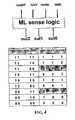
- Each circuit ML SENSE LOGICreceives at its input two pairs of bits generated by the sense amplifiers of a pair of three-level cells and generates a corresponding triplet of bits OUT 2 , OUT 1 , OUT 0 , as shown in FIG. 4 .
- a possible embodiment of the logic circuit ML SENSE LOGICis depicted in FIG. 5 , as will be appreciated by those skilled in the art without requiring any further description of its functioning.
- the logic decoding circuit SL SENSE LOGIChas a logic signal propagation path such that it outputs the least significant bit LSB of the input pair of bits MSB, LSB. This because it is assumed that the two logic levels of the bits are encoded in the threshold voltage levels A and B of the three-level cell, the third level C remaining unused. Alternatively, if the two levels of the bit to be stored were coded in levels A and C of the three-level cell, the same logic decoding circuit SL SENSE LOGIC would output the most significant bit MSB instead.
- a read operationis carried out by reading pairs of three-level cells and decoding the read ternary levels in strings of three bits, according to the coding scheme illustrated in FIG. 4 .
- Programming of the memoryis preceded by a coding step for transforming triplets of bits to be stored in the memory into pairs of ternary levels to be programmed in the cells.
- the base element of a NOR FLASH memory deviceis the word (16 bits), that is the amount of information that users can read and program with a single operation. With more recent memory devices it may be possible to read with a single operation more than a single word, typically 4, 8 or 16 words (this lot of information is called “page”), through the steps of: page mode reading, that includes reading the words of a page with an access time shorter than a first access executed to the same page; and burst mode reading, that includes a sequential reading of the memory cells of the array starting from an initial address.
- Both read modesare possible by a sensing structure capable of reading and storing the content of a page of the device (in burst mode it is helpful to keep synchronous read frequencies larger than the inner access time of the device).
- a simple way of realizing a NOR FLASH memory based on three-level cellsmay comprise splitting each word in five triplets of bits (10 cells of a three-level memory device, logically associated in pairs) plus an eleventh cell destined to store a single bit that could assume only 2 of the 3 possible levels. Being k the number of words of each page, the read circuit includes k*11 sensing elements.
- using one cell out of 11 for storing a single bitmay represent an inefficient use of valuable silicon area.
- strings of N bits to be storedare encoded into corresponding k-level strings having c symbols, and these k-level strings are stored into corresponding groups of c memory cells.
- the number of bits of a wordmay not be an integer multiple of c and thus one or more bits remain.
- the remaining bit or bits of a wordare stored together with the corresponding remaining bits of other words belonging to the same page, in a dedicated group of c cells with k levels.
- a method of managing a memoryemploying three-level cells and a related three-level memory device with a greater information density than known three-level devices. This result is obtained by grouping in triplets the bits of each word of 16 bits and grouping in triplets the remaining bits of the word that comprise the same page, to be stored in respective pairs of three-level cells.
- the methodmay be applied to the case in which the memory cells may assume more than three levels, though in these cases “bit manipulation” may not be guaranteed.
- bit manipulationmay not be guaranteed.
- FIG. 1depicts an architecture of a memory device in which data stored in three-level cells are read in words of sixteen bits, in accordance with the prior art.
- FIG. 2illustrates a sample coding of a word including 16 bits in eleven three-level-cells, in accordance with the prior art.
- FIG. 3illustrates an example of decoding of the program levels of a three-level-cell in a pair of bits MSB, LSB, in accordance with the prior art.
- FIG. 4illustrates how a stored triplet of bits is decoded into a respective pair of three-level cells, in accordance with the prior art.
- FIG. 5illustrates a possible architecture of a logic decoding circuit that implements the decoding scheme of FIG. 4 , in accordance with the prior art.
- FIG. 6illustrates a sample decoding of the program levels of a three-level cell to store one bit and the architecture of a relative decoding circuit, in accordance with the prior art.
- FIG. 7illustrates how the remaining bits of a word of a same page are grouped in triplets to be stored into respective pairs of three-level cells, in accordance with the present invention.
- FIG. 8illustrates how the bits of a same word are grouped in quintuplets to be stored into respective pairs of six-level cells, in accordance with the present invention.
- FIGS. 7 and 8A sample embodiment for the case of a three-level cell memory will now be described by referring to FIGS. 7 and 8 .
- FIG. 7it is possible to achieve a significant reduction of silicon area occupied by the array of memory cells by grouping in triplets the bits of each word and grouping the remaining bit of each word with the remaining bits of other two words such to form triplets to be stored in respective pairs of three-level array cells.
- An advantagemay be in that two cells of three threshold level capability are used for storing the remaining three bits and not three cells with three levels, as according to the method and architectural arrangement disclosed in the above discussed prior patent application.
- This approachis theoretically applicable to multilevel memories using cells with any number of distinct threshold levels.
- the number of cells used for storing information of a page of k wordsdecreases from k*11 to k*16/1.5 (rounded up to the smallest larger integer). For example:
- the silicon area savingis:
- the remaining bit of the wordis not decoded by a circuit as depicted in FIG. 6 , but with a circuit as depicted in FIG. 4 , together with two remaining bits of other two words.
- the bits of each wordare grouped in quintuplets and each quintuplet is stored in a respective pair of six-level cells, as schematically illustrated in FIG. 8 .
- the bits of each wordare grouped in quintuplets and, as for three-level memory devices, there is a remaining bit.
- the remaining bit of each wordis grouped in a quintuplet together with four remaining bits of other words of the same page and this quintuplet is stored in a respective pair of six-level cells.
- the disclosed methodcan be generalized for a memory having cells that may assume one out of k different levels by grouping the cells in sets of c cells and by storing in each c-tuplet of cells a number N of bits given by the following formula:
- Nis not an integer factor of the number of bits ( 16 ) of a word
- these remaining bits of the word of each pagemay be conveniently grouped in sets of N bits to be stored in respective c-tuplets of cells with k levels.
- the coding and decoding circuits of the memorymay convert strings of N bits into strings with k levels and vice versa using an appropriate code.
- the technique of this approachallows to simulate the functioning of a memory with cells with 2 z levels using a memory with cells with a number of levels k smaller than 2 z . This may not be particularly useful when, for technological reasons, it is impractical to realize cells with 2 z levels but it is practicable to realize memory devices with k-level cells, being 2 z ⁇ 1 ⁇ k ⁇ 2 z .
Landscapes
- Engineering & Computer Science (AREA)
- Computer Hardware Design (AREA)
- Read Only Memory (AREA)
- Debugging And Monitoring (AREA)
Abstract
Description
- This invention relates in general to semiconductor memory devices, and, more particularly to a method of managing a memory that employs k-level cells and a related memory device.
- In a multi-level memory device cells generally assume more than two logic states and thus may store information of more than one bit. A multi-level memory device that occupies a silicon area slightly larger than that of a four-level memory device of the same storage capacity is described in the Italian patent application VA2006A000065, assigned to the current assignee. It employs three-level cells whereby each pair of cells is to store a string of three bits and comprises a coding circuit and a decoding circuit for converting, in a write operation, the strings of three bits to be stored, in strings of two ternary values to be written in respective pairs of three-level cells, and vice versa during a read operation.
- There may be three possible states of each cell, thus the relative distributions of the three different read thresholds can be relatively farther away from the voltage levels at which the known “read disturb” and “retention” phenomena (discussed in the above cited prior Italian patent application) are more severe.
- A method of managing a multi-level memory device that addresses the issues caused by an accidental interruption or supply voltage drop of a magnitude capable of stopping an ongoing program operation that could take place during programming and that may render the memory device usable as if it were a two-bit memory device, is also disclosed in the above cited prior Italian patent application.
- According to the three-level memory device disclosed in the prior application, each cell may assume one of three possible logic values, with the advantage of an area occupation significantly smaller than that of a common one-bit-per-cell memory device, though with a reduced number of threshold voltage distributions than a two-bit-per-cell memory device. This may make unnecessary error correction code techniques, that may otherwise be indispensable with present day technology two-bit per cell devices for ensuring an acceptable reliability, and thus the consequent limitations in terms of “bit manipulation” that the use of ECC technique may impose.
- An architecture of the memory device according to the cited prior application is schematically depicted in
FIG. 1 . - Generally, the base element of information of a FLASH memory device is the word that commonly includes 16 bits. To store 16 bits, according to a preferred grouping scheme of the present approach depicted in
FIG. 2 , five pairs of three-level cells are used, with the remainder of one bit that conveniently but not necessarily may be the most significant or the least significant bit, being stored in an eleventh cell destined to store such a remaining single bit. In practice, this last cell may assume only two of the three possible levels. - One of skill in the art will recognize that it is not necessary that the single bit be stored in the three-level cell destined to store a single bit be the most significant or the least significant bit, but that it can be another bit of the word. Referring to the scheme of
FIG. 2 , if for example, thebit 9 is stored in a single three-level cell, then thebits 0 to8 are grouped in triplets as illustrated, and the remaining two triplets of bits may be A, B, C and D, E, F are stored in respective pairs of three-level cells. The three-level memory device as depicted inFIG. 1 , has an array of sense amplifiers S.A., each associated with a respective three-level cell of the word to be read and generating two bits, namely: MSB and LSB, representative of the program level of the cell, preferably according to the coding scheme ofFIG. 3 . - Differently from a classic device, the memory device may have for each word that comprises a page to be read an array of five logic decoding circuits ML SENSE LOGIC, each associated with a respective pair of three-level cells, plus another logic decoding circuit SL SENSE LOGIC, associated with the three-level cell destined to store a single bit.
- Each circuit ML SENSE LOGIC receives at its input two pairs of bits generated by the sense amplifiers of a pair of three-level cells and generates a corresponding triplet of bits OUT2, OUT1, OUT0, as shown in
FIG. 4 . A possible embodiment of the logic circuit ML SENSE LOGIC is depicted inFIG. 5 , as will be appreciated by those skilled in the art without requiring any further description of its functioning. - The logic decoding circuit SL SENSE LOGIC, as depicted in
FIG. 6 , has a logic signal propagation path such that it outputs the least significant bit LSB of the input pair of bits MSB, LSB. This because it is assumed that the two logic levels of the bits are encoded in the threshold voltage levels A and B of the three-level cell, the third level C remaining unused. Alternatively, if the two levels of the bit to be stored were coded in levels A and C of the three-level cell, the same logic decoding circuit SL SENSE LOGIC would output the most significant bit MSB instead. - A read operation is carried out by reading pairs of three-level cells and decoding the read ternary levels in strings of three bits, according to the coding scheme illustrated in
FIG. 4 . Programming of the memory is preceded by a coding step for transforming triplets of bits to be stored in the memory into pairs of ternary levels to be programmed in the cells. - The base element of a NOR FLASH memory device is the word (16 bits), that is the amount of information that users can read and program with a single operation. With more recent memory devices it may be possible to read with a single operation more than a single word, typically 4, 8 or 16 words (this lot of information is called “page”), through the steps of: page mode reading, that includes reading the words of a page with an access time shorter than a first access executed to the same page; and burst mode reading, that includes a sequential reading of the memory cells of the array starting from an initial address.
- Both read modes are possible by a sensing structure capable of reading and storing the content of a page of the device (in burst mode it is helpful to keep synchronous read frequencies larger than the inner access time of the device).
- A simple way of realizing a NOR FLASH memory based on three-level cells may comprise splitting each word in five triplets of bits (10 cells of a three-level memory device, logically associated in pairs) plus an eleventh cell destined to store a single bit that could assume only 2 of the 3 possible levels. Being k the number of words of each page, the read circuit includes k*11 sensing elements.
- In a context of multi-level memory devices, using one cell out of 11 for storing a single bit may represent an inefficient use of valuable silicon area. Being the density of information the ratio between the number of stored bits and the number of used cells, it is 16 bits/11 cells=1.4545 bit/cell, if the number of cells (16) of each word of the device is considered, but the theoretically threshold ratio is 3 bits/2 cells=1.5 bit/cell.
- A more efficient method of managing a memory with cells of k levels that noticeably reduces the above noted area occupation inefficiency and a related multi-level memory device with k-level cells have now been found. As a matter of fact, strings of N bits to be stored are encoded into corresponding k-level strings having c symbols, and these k-level strings are stored into corresponding groups of c memory cells.
- In general, for example in case of three-level memory cells, the number of bits of a word may not be an integer multiple of c and thus one or more bits remain. According to this approach, the remaining bit or bits of a word are stored together with the corresponding remaining bits of other words belonging to the same page, in a dedicated group of c cells with k levels.
- According to a first embodiment, there is a method of managing a memory employing three-level cells and a related three-level memory device with a greater information density than known three-level devices. This result is obtained by grouping in triplets the bits of each word of 16 bits and grouping in triplets the remaining bits of the word that comprise the same page, to be stored in respective pairs of three-level cells.
- The method may be applied to the case in which the memory cells may assume more than three levels, though in these cases “bit manipulation” may not be guaranteed. For example, in case of memory devices employing six-level cells, it is possible to group the bits of each word in quintuplets and to store each quintuplet in a respective pair of six-level cells. If words include 16 bits, there may be a remaining bit that is conveniently grouped with the remaining bits of other four words in a quintuplet to be stored in a dedicated pair of six-level cells.
FIG. 1 depicts an architecture of a memory device in which data stored in three-level cells are read in words of sixteen bits, in accordance with the prior art.FIG. 2 illustrates a sample coding of a word including 16 bits in eleven three-level-cells, in accordance with the prior art.FIG. 3 illustrates an example of decoding of the program levels of a three-level-cell in a pair of bits MSB, LSB, in accordance with the prior art.FIG. 4 illustrates how a stored triplet of bits is decoded into a respective pair of three-level cells, in accordance with the prior art.FIG. 5 illustrates a possible architecture of a logic decoding circuit that implements the decoding scheme ofFIG. 4 , in accordance with the prior art.FIG. 6 illustrates a sample decoding of the program levels of a three-level cell to store one bit and the architecture of a relative decoding circuit, in accordance with the prior art.FIG. 7 illustrates how the remaining bits of a word of a same page are grouped in triplets to be stored into respective pairs of three-level cells, in accordance with the present invention.FIG. 8 illustrates how the bits of a same word are grouped in quintuplets to be stored into respective pairs of six-level cells, in accordance with the present invention.- A sample embodiment for the case of a three-level cell memory will now be described by referring to
FIGS. 7 and 8 . As illustrated inFIG. 7 , it is possible to achieve a significant reduction of silicon area occupied by the array of memory cells by grouping in triplets the bits of each word and grouping the remaining bit of each word with the remaining bits of other two words such to form triplets to be stored in respective pairs of three-level array cells. - An advantage may be in that two cells of three threshold level capability are used for storing the remaining three bits and not three cells with three levels, as according to the method and architectural arrangement disclosed in the above discussed prior patent application. This approach is theoretically applicable to multilevel memories using cells with any number of distinct threshold levels. For the considered case of three-level cells, the number of cells used for storing information of a page of k words decreases from k*11 to k*16/1.5 (rounded up to the smallest larger integer). For example:
- k=4: in the known three-level memory devices44 cells per page are used, while in the proposed three-level memory device43 cells per page are sufficient;
- k=8: in the known three-level memory devices88 cells per page are used, while in the proposed three-level memory device46 cells per page are sufficient;
- k=16: in the known three-level memory devices176 cells per page are used, while in the proposed three-level memory device171 cells per page are sufficient.
- With the proposed method of managing a three-level memory device, the silicon area saving is:
- Differently from the memory device disclosed in the above mentioned Italian patent application No. VA2006A000065, the remaining bit of the word is not decoded by a circuit as depicted in
FIG. 6 , but with a circuit as depicted inFIG. 4 , together with two remaining bits of other two words. - According to another embodiment of the method of this approach, applicable to memory with six-level cells, the bits of each word are grouped in quintuplets and each quintuplet is stored in a respective pair of six-level cells, as schematically illustrated in
FIG. 8 . - Even in this case, there may be states of the pair of cells that are unused, but they are much less numerous than the used states.
- The bits of each word are grouped in quintuplets and, as for three-level memory devices, there is a remaining bit. According to an embodiment, the remaining bit of each word is grouped in a quintuplet together with four remaining bits of other words of the same page and this quintuplet is stored in a respective pair of six-level cells.
- As will be evident to any skilled person, the disclosed method can be generalized for a memory having cells that may assume one out of k different levels by grouping the cells in sets of c cells and by storing in each c-tuplet of cells a number N of bits given by the following formula:
N=int[c·log2k]- wherein the function int[.] truncates its argument. The number c of cells should be chosen to reduce the number of unused states given by kc−2N.
- If N is not an integer factor of the number of bits (16) of a word, in each word there may be one or more remaining bits. By adapting what has been described with reference to three-level cells, these remaining bits of the word of each page may be conveniently grouped in sets of N bits to be stored in respective c-tuplets of cells with k levels.
- In general, the coding and decoding circuits of the memory may convert strings of N bits into strings with k levels and vice versa using an appropriate code.
- The technique of this approach allows to simulate the functioning of a memory with cells with 2zlevels using a memory with cells with a number of levels k smaller than 2z. This may not be particularly useful when, for technological reasons, it is impractical to realize cells with 2zlevels but it is practicable to realize memory devices with k-level cells, being 2z−1<k<2z.
Claims (19)
Applications Claiming Priority (3)
| Application Number | Priority Date | Filing Date | Title |
|---|---|---|---|
| ITVA2007A0042 | 2007-04-27 | ||
| IT000042AITVA20070042A1 (en) | 2007-04-27 | 2007-04-27 | METHOD OF MANAGEMENT OF A MEMORY DEVICE AND ITS MEMORY DEVICE |
| ITVA2007A000042 | 2007-04-27 |
Publications (2)
| Publication Number | Publication Date |
|---|---|
| US20080266946A1true US20080266946A1 (en) | 2008-10-30 |
| US7710772B2 US7710772B2 (en) | 2010-05-04 |
Family
ID=39886778
Family Applications (1)
| Application Number | Title | Priority Date | Filing Date |
|---|---|---|---|
| US12/109,525Active2028-09-01US7710772B2 (en) | 2007-04-27 | 2008-04-25 | Method of managing a multilevel memory device and related device |
Country Status (2)
| Country | Link |
|---|---|
| US (1) | US7710772B2 (en) |
| IT (1) | ITVA20070042A1 (en) |
Cited By (2)
| Publication number | Priority date | Publication date | Assignee | Title |
|---|---|---|---|---|
| US20080212369A1 (en)* | 2007-03-02 | 2008-09-04 | Stmicroelectronics S.R.L. | Method of managing a memory device employing three-level cells |
| US9570174B2 (en) | 2013-10-14 | 2017-02-14 | Samsung Electronics Co., Ltd. | Coding method and decoding method in memory system |
Families Citing this family (1)
| Publication number | Priority date | Publication date | Assignee | Title |
|---|---|---|---|---|
| US8737139B2 (en) | 2012-04-11 | 2014-05-27 | Micron Technology, Inc. | Determining soft data for combinations of memory cells |
Citations (11)
| Publication number | Priority date | Publication date | Assignee | Title |
|---|---|---|---|---|
| US5838610A (en)* | 1996-02-07 | 1998-11-17 | Nec Corporation | Semiconductor memory device having multilevel memory cell array |
| US5838968A (en)* | 1996-03-01 | 1998-11-17 | Chromatic Research, Inc. | System and method for dynamic resource management across tasks in real-time operating systems |
| US5973958A (en)* | 1998-06-23 | 1999-10-26 | Advanced Micro Devices, Inc. | Interlaced storage and sense technique for flash multi-level devices |
| US6208542B1 (en)* | 1998-06-30 | 2001-03-27 | Sandisk Corporation | Techniques for storing digital data in an analog or multilevel memory |
| US6324550B1 (en)* | 1999-08-25 | 2001-11-27 | Bullant Technology Pty Ltd | Data object identification and removal system |
| US6789215B1 (en)* | 2000-04-21 | 2004-09-07 | Sprint Communications Company, L.P. | System and method for remediating a computer |
| US6948166B2 (en)* | 2001-04-05 | 2005-09-20 | International Business Machines Corporation | System and method for automatically de-installing previously installed software based on user defined preferences |
| US20060036735A1 (en)* | 2004-07-29 | 2006-02-16 | International Business Machines Corporation | Method for avoiding unnecessary provisioning/deprovisioning of resources in a utility services environment |
| US7028305B2 (en)* | 2001-05-16 | 2006-04-11 | Softricity, Inc. | Operating system abstraction and protection layer |
| US7185335B2 (en)* | 2002-09-19 | 2007-02-27 | International Business Machines Corporation | Programmatic application installation diagnosis and cleaning |
| US20070220321A1 (en)* | 2006-02-14 | 2007-09-20 | International Business Machines Corporation | Method, apparatus and program product for a point-in-time recovery of a computing system |
- 2007
- 2007-04-27ITIT000042Apatent/ITVA20070042A1/enunknown
- 2008
- 2008-04-25USUS12/109,525patent/US7710772B2/enactiveActive
Patent Citations (11)
| Publication number | Priority date | Publication date | Assignee | Title |
|---|---|---|---|---|
| US5838610A (en)* | 1996-02-07 | 1998-11-17 | Nec Corporation | Semiconductor memory device having multilevel memory cell array |
| US5838968A (en)* | 1996-03-01 | 1998-11-17 | Chromatic Research, Inc. | System and method for dynamic resource management across tasks in real-time operating systems |
| US5973958A (en)* | 1998-06-23 | 1999-10-26 | Advanced Micro Devices, Inc. | Interlaced storage and sense technique for flash multi-level devices |
| US6208542B1 (en)* | 1998-06-30 | 2001-03-27 | Sandisk Corporation | Techniques for storing digital data in an analog or multilevel memory |
| US6324550B1 (en)* | 1999-08-25 | 2001-11-27 | Bullant Technology Pty Ltd | Data object identification and removal system |
| US6789215B1 (en)* | 2000-04-21 | 2004-09-07 | Sprint Communications Company, L.P. | System and method for remediating a computer |
| US6948166B2 (en)* | 2001-04-05 | 2005-09-20 | International Business Machines Corporation | System and method for automatically de-installing previously installed software based on user defined preferences |
| US7028305B2 (en)* | 2001-05-16 | 2006-04-11 | Softricity, Inc. | Operating system abstraction and protection layer |
| US7185335B2 (en)* | 2002-09-19 | 2007-02-27 | International Business Machines Corporation | Programmatic application installation diagnosis and cleaning |
| US20060036735A1 (en)* | 2004-07-29 | 2006-02-16 | International Business Machines Corporation | Method for avoiding unnecessary provisioning/deprovisioning of resources in a utility services environment |
| US20070220321A1 (en)* | 2006-02-14 | 2007-09-20 | International Business Machines Corporation | Method, apparatus and program product for a point-in-time recovery of a computing system |
Cited By (3)
| Publication number | Priority date | Publication date | Assignee | Title |
|---|---|---|---|---|
| US20080212369A1 (en)* | 2007-03-02 | 2008-09-04 | Stmicroelectronics S.R.L. | Method of managing a memory device employing three-level cells |
| US7782665B2 (en) | 2007-03-02 | 2010-08-24 | Paolo Turbanti | Method of managing a memory device employing three-level cells |
| US9570174B2 (en) | 2013-10-14 | 2017-02-14 | Samsung Electronics Co., Ltd. | Coding method and decoding method in memory system |
Also Published As
| Publication number | Publication date |
|---|---|
| ITVA20070042A1 (en) | 2008-10-28 |
| US7710772B2 (en) | 2010-05-04 |
Similar Documents
| Publication | Publication Date | Title |
|---|---|---|
| US6646913B2 (en) | Method for storing and reading data in a multilevel nonvolatile memory | |
| US5539690A (en) | Write verify schemes for flash memory with multilevel cells | |
| US8136014B2 (en) | Non-volatile semiconductor memory device | |
| US9502120B2 (en) | Programming memory cells dependent upon distortion estimation | |
| KR101675170B1 (en) | Methods and apparatus for intercell interference mitigation using modulation coding | |
| US7071849B2 (en) | Fractional-Bit Systems | |
| US6674385B2 (en) | Analog-to-digital conversion method and device, in high-density multilevel non-volatile memory devices | |
| US8458416B2 (en) | Systems and methods for selecting bit per cell density of a memory cell based on data typing | |
| TW201007739A (en) | Multiple-bit per Cell (MBC) non-volatile memory apparatus and system having polarity control and method of programming same | |
| US20050063219A1 (en) | Multilevel memory device with memory cells storing non-power of two voltage levels | |
| JP2000251484A (en) | Non-volatile semiconductor memory | |
| US7596023B2 (en) | Memory device employing three-level cells and related methods of managing | |
| US20030086302A1 (en) | Data write/read control method and memory device | |
| US7710772B2 (en) | Method of managing a multilevel memory device and related device | |
| KR100272153B1 (en) | 3 value memory system | |
| KR20090098439A (en) | Nonvolatile Memory Devices | |
| US6483743B1 (en) | Multilevel cell memory architecture | |
| JP2007157234A (en) | Memory system | |
| CN115862710A (en) | Control method for NAND flash memory to realize exclusive OR operation | |
| EP2707879B1 (en) | Programming memory cells | |
| US7626867B2 (en) | Method for accessing memory by way of step-increasing threshold voltage | |
| KR100871694B1 (en) | Program method and data read method of non-volatile memory device using six threshold voltage levels, and non-volatile memory device using the same | |
| CN101740125A (en) | Read-write methods of NAND type flash memory and relevant page buffer thereof | |
| CN101350219B (en) | Memory access method | |
| KR19990003406A (en) | Memory device having multi-level cells and data writing method thereof |
Legal Events
| Date | Code | Title | Description |
|---|---|---|---|
| AS | Assignment | Owner name:STMICROELECTRONICS S.R.L., ITALY Free format text:ASSIGNMENT OF ASSIGNORS INTEREST;ASSIGNORS:MAGNAVACCA, ALESSANDRO;PIPITONE, FRANCESCO;LISI, CARLO;AND OTHERS;REEL/FRAME:021210/0644;SIGNING DATES FROM 20080402 TO 20080422 Owner name:STMICROELECTRONICS S.R.L.,ITALY Free format text:ASSIGNMENT OF ASSIGNORS INTEREST;ASSIGNORS:MAGNAVACCA, ALESSANDRO;PIPITONE, FRANCESCO;LISI, CARLO;AND OTHERS;SIGNING DATES FROM 20080402 TO 20080422;REEL/FRAME:021210/0644 | |
| STCF | Information on status: patent grant | Free format text:PATENTED CASE | |
| AS | Assignment | Owner name:MICRON TECHNOLOGY, INC., IDAHO Free format text:ASSIGNMENT OF ASSIGNORS INTEREST;ASSIGNOR:STMICROELECTRONICS S.R.L.;REEL/FRAME:028803/0471 Effective date:20120523 | |
| FPAY | Fee payment | Year of fee payment:4 | |
| AS | Assignment | Owner name:U.S. BANK NATIONAL ASSOCIATION, AS COLLATERAL AGENT, CALIFORNIA Free format text:SECURITY INTEREST;ASSIGNOR:MICRON TECHNOLOGY, INC.;REEL/FRAME:038669/0001 Effective date:20160426 Owner name:U.S. BANK NATIONAL ASSOCIATION, AS COLLATERAL AGEN Free format text:SECURITY INTEREST;ASSIGNOR:MICRON TECHNOLOGY, INC.;REEL/FRAME:038669/0001 Effective date:20160426 | |
| AS | Assignment | Owner name:MORGAN STANLEY SENIOR FUNDING, INC., AS COLLATERAL AGENT, MARYLAND Free format text:PATENT SECURITY AGREEMENT;ASSIGNOR:MICRON TECHNOLOGY, INC.;REEL/FRAME:038954/0001 Effective date:20160426 Owner name:MORGAN STANLEY SENIOR FUNDING, INC., AS COLLATERAL Free format text:PATENT SECURITY AGREEMENT;ASSIGNOR:MICRON TECHNOLOGY, INC.;REEL/FRAME:038954/0001 Effective date:20160426 | |
| AS | Assignment | Owner name:U.S. BANK NATIONAL ASSOCIATION, AS COLLATERAL AGENT, CALIFORNIA Free format text:CORRECTIVE ASSIGNMENT TO CORRECT THE REPLACE ERRONEOUSLY FILED PATENT #7358718 WITH THE CORRECT PATENT #7358178 PREVIOUSLY RECORDED ON REEL 038669 FRAME 0001. ASSIGNOR(S) HEREBY CONFIRMS THE SECURITY INTEREST;ASSIGNOR:MICRON TECHNOLOGY, INC.;REEL/FRAME:043079/0001 Effective date:20160426 Owner name:U.S. BANK NATIONAL ASSOCIATION, AS COLLATERAL AGEN Free format text:CORRECTIVE ASSIGNMENT TO CORRECT THE REPLACE ERRONEOUSLY FILED PATENT #7358718 WITH THE CORRECT PATENT #7358178 PREVIOUSLY RECORDED ON REEL 038669 FRAME 0001. ASSIGNOR(S) HEREBY CONFIRMS THE SECURITY INTEREST;ASSIGNOR:MICRON TECHNOLOGY, INC.;REEL/FRAME:043079/0001 Effective date:20160426 | |
| MAFP | Maintenance fee payment | Free format text:PAYMENT OF MAINTENANCE FEE, 8TH YEAR, LARGE ENTITY (ORIGINAL EVENT CODE: M1552) Year of fee payment:8 | |
| AS | Assignment | Owner name:JPMORGAN CHASE BANK, N.A., AS COLLATERAL AGENT, ILLINOIS Free format text:SECURITY INTEREST;ASSIGNORS:MICRON TECHNOLOGY, INC.;MICRON SEMICONDUCTOR PRODUCTS, INC.;REEL/FRAME:047540/0001 Effective date:20180703 Owner name:JPMORGAN CHASE BANK, N.A., AS COLLATERAL AGENT, IL Free format text:SECURITY INTEREST;ASSIGNORS:MICRON TECHNOLOGY, INC.;MICRON SEMICONDUCTOR PRODUCTS, INC.;REEL/FRAME:047540/0001 Effective date:20180703 | |
| AS | Assignment | Owner name:MICRON TECHNOLOGY, INC., IDAHO Free format text:RELEASE BY SECURED PARTY;ASSIGNOR:U.S. BANK NATIONAL ASSOCIATION, AS COLLATERAL AGENT;REEL/FRAME:047243/0001 Effective date:20180629 | |
| AS | Assignment | Owner name:MICRON TECHNOLOGY, INC., IDAHO Free format text:RELEASE BY SECURED PARTY;ASSIGNOR:MORGAN STANLEY SENIOR FUNDING, INC., AS COLLATERAL AGENT;REEL/FRAME:050937/0001 Effective date:20190731 | |
| AS | Assignment | Owner name:MICRON TECHNOLOGY, INC., IDAHO Free format text:RELEASE BY SECURED PARTY;ASSIGNOR:JPMORGAN CHASE BANK, N.A., AS COLLATERAL AGENT;REEL/FRAME:051028/0001 Effective date:20190731 Owner name:MICRON SEMICONDUCTOR PRODUCTS, INC., IDAHO Free format text:RELEASE BY SECURED PARTY;ASSIGNOR:JPMORGAN CHASE BANK, N.A., AS COLLATERAL AGENT;REEL/FRAME:051028/0001 Effective date:20190731 | |
| MAFP | Maintenance fee payment | Free format text:PAYMENT OF MAINTENANCE FEE, 12TH YEAR, LARGE ENTITY (ORIGINAL EVENT CODE: M1553); ENTITY STATUS OF PATENT OWNER: LARGE ENTITY Year of fee payment:12 |