US20080258168A1 - Semiconductor light emitting device packages and methods - Google Patents
Semiconductor light emitting device packages and methodsDownload PDFInfo
- Publication number
- US20080258168A1 US20080258168A1US11/788,001US78800107AUS2008258168A1US 20080258168 A1US20080258168 A1US 20080258168A1US 78800107 AUS78800107 AUS 78800107AUS 2008258168 A1US2008258168 A1US 2008258168A1
- Authority
- US
- United States
- Prior art keywords
- substrate
- bond pad
- pad
- corner
- solder
- Prior art date
- Legal status (The legal status is an assumption and is not a legal conclusion. Google has not performed a legal analysis and makes no representation as to the accuracy of the status listed.)
- Granted
Links
Images


Classifications
- H—ELECTRICITY
- H10—SEMICONDUCTOR DEVICES; ELECTRIC SOLID-STATE DEVICES NOT OTHERWISE PROVIDED FOR
- H10H—INORGANIC LIGHT-EMITTING SEMICONDUCTOR DEVICES HAVING POTENTIAL BARRIERS
- H10H20/00—Individual inorganic light-emitting semiconductor devices having potential barriers, e.g. light-emitting diodes [LED]
- H10H20/80—Constructional details
- H10H20/85—Packages
- H10H20/852—Encapsulations
- H—ELECTRICITY
- H01—ELECTRIC ELEMENTS
- H01L—SEMICONDUCTOR DEVICES NOT COVERED BY CLASS H10
- H01L24/00—Arrangements for connecting or disconnecting semiconductor or solid-state bodies; Methods or apparatus related thereto
- H01L24/93—Batch processes
- H01L24/95—Batch processes at chip-level, i.e. with connecting carried out on a plurality of singulated devices, i.e. on diced chips
- H01L24/97—Batch processes at chip-level, i.e. with connecting carried out on a plurality of singulated devices, i.e. on diced chips the devices being connected to a common substrate, e.g. interposer, said common substrate being separable into individual assemblies after connecting
- H—ELECTRICITY
- H10—SEMICONDUCTOR DEVICES; ELECTRIC SOLID-STATE DEVICES NOT OTHERWISE PROVIDED FOR
- H10H—INORGANIC LIGHT-EMITTING SEMICONDUCTOR DEVICES HAVING POTENTIAL BARRIERS
- H10H20/00—Individual inorganic light-emitting semiconductor devices having potential barriers, e.g. light-emitting diodes [LED]
- H10H20/80—Constructional details
- H10H20/85—Packages
- H10H20/8506—Containers
- H—ELECTRICITY
- H10—SEMICONDUCTOR DEVICES; ELECTRIC SOLID-STATE DEVICES NOT OTHERWISE PROVIDED FOR
- H10H—INORGANIC LIGHT-EMITTING SEMICONDUCTOR DEVICES HAVING POTENTIAL BARRIERS
- H10H20/00—Individual inorganic light-emitting semiconductor devices having potential barriers, e.g. light-emitting diodes [LED]
- H10H20/80—Constructional details
- H10H20/85—Packages
- H10H20/857—Interconnections, e.g. lead-frames, bond wires or solder balls
- H—ELECTRICITY
- H01—ELECTRIC ELEMENTS
- H01L—SEMICONDUCTOR DEVICES NOT COVERED BY CLASS H10
- H01L2224/00—Indexing scheme for arrangements for connecting or disconnecting semiconductor or solid-state bodies and methods related thereto as covered by H01L24/00
- H01L2224/01—Means for bonding being attached to, or being formed on, the surface to be connected, e.g. chip-to-package, die-attach, "first-level" interconnects; Manufacturing methods related thereto
- H01L2224/26—Layer connectors, e.g. plate connectors, solder or adhesive layers; Manufacturing methods related thereto
- H01L2224/31—Structure, shape, material or disposition of the layer connectors after the connecting process
- H01L2224/32—Structure, shape, material or disposition of the layer connectors after the connecting process of an individual layer connector
- H01L2224/321—Disposition
- H01L2224/32151—Disposition the layer connector connecting between a semiconductor or solid-state body and an item not being a semiconductor or solid-state body, e.g. chip-to-substrate, chip-to-passive
- H01L2224/32221—Disposition the layer connector connecting between a semiconductor or solid-state body and an item not being a semiconductor or solid-state body, e.g. chip-to-substrate, chip-to-passive the body and the item being stacked
- H01L2224/32245—Disposition the layer connector connecting between a semiconductor or solid-state body and an item not being a semiconductor or solid-state body, e.g. chip-to-substrate, chip-to-passive the body and the item being stacked the item being metallic
- H01L2224/32257—Disposition the layer connector connecting between a semiconductor or solid-state body and an item not being a semiconductor or solid-state body, e.g. chip-to-substrate, chip-to-passive the body and the item being stacked the item being metallic the layer connector connecting to a bonding area disposed in a recess of the surface of the item
- H—ELECTRICITY
- H01—ELECTRIC ELEMENTS
- H01L—SEMICONDUCTOR DEVICES NOT COVERED BY CLASS H10
- H01L2224/00—Indexing scheme for arrangements for connecting or disconnecting semiconductor or solid-state bodies and methods related thereto as covered by H01L24/00
- H01L2224/01—Means for bonding being attached to, or being formed on, the surface to be connected, e.g. chip-to-package, die-attach, "first-level" interconnects; Manufacturing methods related thereto
- H01L2224/42—Wire connectors; Manufacturing methods related thereto
- H01L2224/44—Structure, shape, material or disposition of the wire connectors prior to the connecting process
- H01L2224/45—Structure, shape, material or disposition of the wire connectors prior to the connecting process of an individual wire connector
- H01L2224/45001—Core members of the connector
- H01L2224/45099—Material
- H01L2224/451—Material with a principal constituent of the material being a metal or a metalloid, e.g. boron (B), silicon (Si), germanium (Ge), arsenic (As), antimony (Sb), tellurium (Te) and polonium (Po), and alloys thereof
- H01L2224/45117—Material with a principal constituent of the material being a metal or a metalloid, e.g. boron (B), silicon (Si), germanium (Ge), arsenic (As), antimony (Sb), tellurium (Te) and polonium (Po), and alloys thereof the principal constituent melting at a temperature of greater than or equal to 400°C and less than 950°C
- H01L2224/45124—Aluminium (Al) as principal constituent
- H—ELECTRICITY
- H01—ELECTRIC ELEMENTS
- H01L—SEMICONDUCTOR DEVICES NOT COVERED BY CLASS H10
- H01L2224/00—Indexing scheme for arrangements for connecting or disconnecting semiconductor or solid-state bodies and methods related thereto as covered by H01L24/00
- H01L2224/01—Means for bonding being attached to, or being formed on, the surface to be connected, e.g. chip-to-package, die-attach, "first-level" interconnects; Manufacturing methods related thereto
- H01L2224/42—Wire connectors; Manufacturing methods related thereto
- H01L2224/47—Structure, shape, material or disposition of the wire connectors after the connecting process
- H01L2224/48—Structure, shape, material or disposition of the wire connectors after the connecting process of an individual wire connector
- H01L2224/4805—Shape
- H01L2224/4809—Loop shape
- H01L2224/48091—Arched
- H—ELECTRICITY
- H01—ELECTRIC ELEMENTS
- H01L—SEMICONDUCTOR DEVICES NOT COVERED BY CLASS H10
- H01L2224/00—Indexing scheme for arrangements for connecting or disconnecting semiconductor or solid-state bodies and methods related thereto as covered by H01L24/00
- H01L2224/01—Means for bonding being attached to, or being formed on, the surface to be connected, e.g. chip-to-package, die-attach, "first-level" interconnects; Manufacturing methods related thereto
- H01L2224/42—Wire connectors; Manufacturing methods related thereto
- H01L2224/47—Structure, shape, material or disposition of the wire connectors after the connecting process
- H01L2224/48—Structure, shape, material or disposition of the wire connectors after the connecting process of an individual wire connector
- H01L2224/481—Disposition
- H01L2224/48151—Connecting between a semiconductor or solid-state body and an item not being a semiconductor or solid-state body, e.g. chip-to-substrate, chip-to-passive
- H01L2224/48221—Connecting between a semiconductor or solid-state body and an item not being a semiconductor or solid-state body, e.g. chip-to-substrate, chip-to-passive the body and the item being stacked
- H01L2224/48225—Connecting between a semiconductor or solid-state body and an item not being a semiconductor or solid-state body, e.g. chip-to-substrate, chip-to-passive the body and the item being stacked the item being non-metallic, e.g. insulating substrate with or without metallisation
- H01L2224/48227—Connecting between a semiconductor or solid-state body and an item not being a semiconductor or solid-state body, e.g. chip-to-substrate, chip-to-passive the body and the item being stacked the item being non-metallic, e.g. insulating substrate with or without metallisation connecting the wire to a bond pad of the item
- H—ELECTRICITY
- H01—ELECTRIC ELEMENTS
- H01L—SEMICONDUCTOR DEVICES NOT COVERED BY CLASS H10
- H01L2224/00—Indexing scheme for arrangements for connecting or disconnecting semiconductor or solid-state bodies and methods related thereto as covered by H01L24/00
- H01L2224/01—Means for bonding being attached to, or being formed on, the surface to be connected, e.g. chip-to-package, die-attach, "first-level" interconnects; Manufacturing methods related thereto
- H01L2224/42—Wire connectors; Manufacturing methods related thereto
- H01L2224/47—Structure, shape, material or disposition of the wire connectors after the connecting process
- H01L2224/48—Structure, shape, material or disposition of the wire connectors after the connecting process of an individual wire connector
- H01L2224/481—Disposition
- H01L2224/48151—Connecting between a semiconductor or solid-state body and an item not being a semiconductor or solid-state body, e.g. chip-to-substrate, chip-to-passive
- H01L2224/48221—Connecting between a semiconductor or solid-state body and an item not being a semiconductor or solid-state body, e.g. chip-to-substrate, chip-to-passive the body and the item being stacked
- H01L2224/48245—Connecting between a semiconductor or solid-state body and an item not being a semiconductor or solid-state body, e.g. chip-to-substrate, chip-to-passive the body and the item being stacked the item being metallic
- H01L2224/48247—Connecting between a semiconductor or solid-state body and an item not being a semiconductor or solid-state body, e.g. chip-to-substrate, chip-to-passive the body and the item being stacked the item being metallic connecting the wire to a bond pad of the item
- H—ELECTRICITY
- H01—ELECTRIC ELEMENTS
- H01L—SEMICONDUCTOR DEVICES NOT COVERED BY CLASS H10
- H01L2224/00—Indexing scheme for arrangements for connecting or disconnecting semiconductor or solid-state bodies and methods related thereto as covered by H01L24/00
- H01L2224/01—Means for bonding being attached to, or being formed on, the surface to be connected, e.g. chip-to-package, die-attach, "first-level" interconnects; Manufacturing methods related thereto
- H01L2224/42—Wire connectors; Manufacturing methods related thereto
- H01L2224/47—Structure, shape, material or disposition of the wire connectors after the connecting process
- H01L2224/48—Structure, shape, material or disposition of the wire connectors after the connecting process of an individual wire connector
- H01L2224/484—Connecting portions
- H01L2224/4847—Connecting portions the connecting portion on the bonding area of the semiconductor or solid-state body being a wedge bond
- H01L2224/48471—Connecting portions the connecting portion on the bonding area of the semiconductor or solid-state body being a wedge bond the other connecting portion not on the bonding area being a ball bond, i.e. wedge-to-ball, reverse stitch
- H—ELECTRICITY
- H01—ELECTRIC ELEMENTS
- H01L—SEMICONDUCTOR DEVICES NOT COVERED BY CLASS H10
- H01L2224/00—Indexing scheme for arrangements for connecting or disconnecting semiconductor or solid-state bodies and methods related thereto as covered by H01L24/00
- H01L2224/01—Means for bonding being attached to, or being formed on, the surface to be connected, e.g. chip-to-package, die-attach, "first-level" interconnects; Manufacturing methods related thereto
- H01L2224/42—Wire connectors; Manufacturing methods related thereto
- H01L2224/47—Structure, shape, material or disposition of the wire connectors after the connecting process
- H01L2224/49—Structure, shape, material or disposition of the wire connectors after the connecting process of a plurality of wire connectors
- H01L2224/491—Disposition
- H01L2224/4911—Disposition the connectors being bonded to at least one common bonding area, e.g. daisy chain
- H01L2224/49113—Disposition the connectors being bonded to at least one common bonding area, e.g. daisy chain the connectors connecting different bonding areas on the semiconductor or solid-state body to a common bonding area outside the body, e.g. converging wires
- H—ELECTRICITY
- H01—ELECTRIC ELEMENTS
- H01L—SEMICONDUCTOR DEVICES NOT COVERED BY CLASS H10
- H01L2224/00—Indexing scheme for arrangements for connecting or disconnecting semiconductor or solid-state bodies and methods related thereto as covered by H01L24/00
- H01L2224/73—Means for bonding being of different types provided for in two or more of groups H01L2224/10, H01L2224/18, H01L2224/26, H01L2224/34, H01L2224/42, H01L2224/50, H01L2224/63, H01L2224/71
- H01L2224/732—Location after the connecting process
- H01L2224/73251—Location after the connecting process on different surfaces
- H01L2224/73265—Layer and wire connectors
- H—ELECTRICITY
- H01—ELECTRIC ELEMENTS
- H01L—SEMICONDUCTOR DEVICES NOT COVERED BY CLASS H10
- H01L2224/00—Indexing scheme for arrangements for connecting or disconnecting semiconductor or solid-state bodies and methods related thereto as covered by H01L24/00
- H01L2224/93—Batch processes
- H01L2224/95—Batch processes at chip-level, i.e. with connecting carried out on a plurality of singulated devices, i.e. on diced chips
- H01L2224/97—Batch processes at chip-level, i.e. with connecting carried out on a plurality of singulated devices, i.e. on diced chips the devices being connected to a common substrate, e.g. interposer, said common substrate being separable into individual assemblies after connecting
- H—ELECTRICITY
- H01—ELECTRIC ELEMENTS
- H01L—SEMICONDUCTOR DEVICES NOT COVERED BY CLASS H10
- H01L25/00—Assemblies consisting of a plurality of semiconductor or other solid state devices
- H01L25/16—Assemblies consisting of a plurality of semiconductor or other solid state devices the devices being of types provided for in two or more different subclasses of H10B, H10D, H10F, H10H, H10K or H10N, e.g. forming hybrid circuits
- H01L25/167—Assemblies consisting of a plurality of semiconductor or other solid state devices the devices being of types provided for in two or more different subclasses of H10B, H10D, H10F, H10H, H10K or H10N, e.g. forming hybrid circuits comprising optoelectronic devices, e.g. LED, photodiodes
- H—ELECTRICITY
- H01—ELECTRIC ELEMENTS
- H01L—SEMICONDUCTOR DEVICES NOT COVERED BY CLASS H10
- H01L2924/00—Indexing scheme for arrangements or methods for connecting or disconnecting semiconductor or solid-state bodies as covered by H01L24/00
- H01L2924/0001—Technical content checked by a classifier
- H01L2924/00014—Technical content checked by a classifier the subject-matter covered by the group, the symbol of which is combined with the symbol of this group, being disclosed without further technical details
- H—ELECTRICITY
- H01—ELECTRIC ELEMENTS
- H01L—SEMICONDUCTOR DEVICES NOT COVERED BY CLASS H10
- H01L2924/00—Indexing scheme for arrangements or methods for connecting or disconnecting semiconductor or solid-state bodies as covered by H01L24/00
- H01L2924/013—Alloys
- H01L2924/0132—Binary Alloys
- H01L2924/01322—Eutectic Alloys, i.e. obtained by a liquid transforming into two solid phases
- H—ELECTRICITY
- H01—ELECTRIC ELEMENTS
- H01L—SEMICONDUCTOR DEVICES NOT COVERED BY CLASS H10
- H01L2924/00—Indexing scheme for arrangements or methods for connecting or disconnecting semiconductor or solid-state bodies as covered by H01L24/00
- H01L2924/10—Details of semiconductor or other solid state devices to be connected
- H01L2924/11—Device type
- H01L2924/12—Passive devices, e.g. 2 terminal devices
- H01L2924/1204—Optical Diode
- H01L2924/12041—LED
- H—ELECTRICITY
- H01—ELECTRIC ELEMENTS
- H01L—SEMICONDUCTOR DEVICES NOT COVERED BY CLASS H10
- H01L2924/00—Indexing scheme for arrangements or methods for connecting or disconnecting semiconductor or solid-state bodies as covered by H01L24/00
- H01L2924/10—Details of semiconductor or other solid state devices to be connected
- H01L2924/11—Device type
- H01L2924/12—Passive devices, e.g. 2 terminal devices
- H01L2924/1204—Optical Diode
- H01L2924/12042—LASER
- H—ELECTRICITY
- H01—ELECTRIC ELEMENTS
- H01L—SEMICONDUCTOR DEVICES NOT COVERED BY CLASS H10
- H01L2924/00—Indexing scheme for arrangements or methods for connecting or disconnecting semiconductor or solid-state bodies as covered by H01L24/00
- H01L2924/10—Details of semiconductor or other solid state devices to be connected
- H01L2924/11—Device type
- H01L2924/14—Integrated circuits
- H—ELECTRICITY
- H01—ELECTRIC ELEMENTS
- H01L—SEMICONDUCTOR DEVICES NOT COVERED BY CLASS H10
- H01L2924/00—Indexing scheme for arrangements or methods for connecting or disconnecting semiconductor or solid-state bodies as covered by H01L24/00
- H01L2924/15—Details of package parts other than the semiconductor or other solid state devices to be connected
- H01L2924/181—Encapsulation
- H01L2924/1815—Shape
- H—ELECTRICITY
- H10—SEMICONDUCTOR DEVICES; ELECTRIC SOLID-STATE DEVICES NOT OTHERWISE PROVIDED FOR
- H10H—INORGANIC LIGHT-EMITTING SEMICONDUCTOR DEVICES HAVING POTENTIAL BARRIERS
- H10H20/00—Individual inorganic light-emitting semiconductor devices having potential barriers, e.g. light-emitting diodes [LED]
- H10H20/80—Constructional details
- H10H20/85—Packages
- H10H20/852—Encapsulations
- H10H20/853—Encapsulations characterised by their shape
Definitions
- This inventionrelates to semiconductor light emitting devices, and more particularly to packages for semiconductor light emitting devices.
- Light emitting diodes and laser diodesare well known solid state electronic devices capable of generating light upon application of a sufficient voltage.
- Light emitting diodes and laser diodesmay be generally referred to as light emitting devices (LEDs).
- LEDslight emitting devices
- Light emitting devicesgenerally include a p-n junction formed in an epitaxial layer grown on a substrate such as sapphire, silicon, silicon carbide, gallium arsenide and the like. The wavelength distribution of the light generated by the LED depends on the material from which the p-n junction is fabricated and the structure of the thin epitaxial layers that include the active region of the device.
- an LEDtypically includes a substrate, an n-type epitaxial region formed on the substrate and a p-type epitaxial region formed on the n-type epitaxial region (or vice-versa).
- an anode ohmic contactis formed on a p-type region of the device (typically, an exposed p-type epitaxial layer) and a cathode ohmic contact is formed on an n-type region of the device (such as the substrate or an exposed n-type epitaxial layer).
- An LED packagealso includes means, such as electrical leads, for electrically connecting the LED chip to an external circuit.
- an LED 12is mounted on a reflective cup 13 by means of a solder bond or epoxy.
- One or more wirebondsconnect the ohmic contacts of the LED to leads 15 A, 15 B which may be attached to or integral with the reflective cup 13 .
- the entire assemblyis then encapsulated in a clear protective resin 14 which may be molded in the shape of a lens to collimate the light emitted from the LED chip 12 .
- a plurality of LED chips 22are mounted onto a printed circuit board (PCB) carrier 23 .
- PCBprinted circuit board
- One or more wirebond connectionsare made between ohmic contacts on the LEDs 22 and electrical traces 25 A, 25 B on the PCB 23 .
- Each mounted LED 22is then covered with a drop of clear resin 24 which may provide environmental and mechanical protection to the chip while also acting as a lens.
- the individual packaged LEDs 22are then separated by sawing the PCB board 23 into small squares, each of which contains one or more LED chips 22 .
- One figure of merit for users of light emitting devicesis cost per lumen, that is, the cost of obtaining a given level of light output.
- the high cost of conventional packaging techniquesmay be one factor that keeps the cost per lumen of solid state lighting relatively high.
- conventional packaging techniquesmay result in large, bulky packages that are unsuitable for certain miniaturized applications such as cellular telephone backlights.
- Conventional packaging techniquesmay also have poor thermal resistance characteristics that limit the power levels at which the LED chip may be driven and place constraints on system designers with respect to placement of LEDs.
- Some embodiments of the inventionprovide a submount for a light emitting device package.
- the submountincludes a generally rectangular substrate having a first surface and a second surface opposite the first surface, a first end and a second end opposite the first end.
- a first bond pad and a second bond padare on the first surface of the substrate.
- the first bond padmay include a die attach region offset toward the first end of the substrate and configured to receive a light emitting diode thereon.
- the second bond padmay include a bonding region that is between the first bond pad and the second end of the substrate and a second bond pad extension that extends from the bonding region along a side of the substrate toward a corner of the substrate at the first end of the substrate.
- the substratefurther includes first and second solder pads on the second surface of the substrate.
- the first solder padis adjacent the first end of the substrate and the second solder pad is adjacent the second end of the substrate.
- the second bond padis in electrical contact with the first solder pad, and the first bond pad is in electrical contact with the second solder pad.
- the substratemay include a castellation at the corner of the substrate and an electrical trace on the castellation that extends from the first surface of the substrate to the second surface of the substrate and that electrically connects the second bond pad and the first solder pad.
- the side of the substratemay include a first side and the corner of the substrate may include a first corner, and the first bond pad may further include a first bond pad extension that extends from the die attach region along a second side of the substrate, opposite the first side of the substrate, towards a second corner of the substrate at the second end of the substrate and diagonally opposed to the first corner.
- the substratemay include a castellation at the second corner of the substrate.
- a second electrical tracemay be on the second castellation and may extend from the first surface of the substrate to the second surface of the substrate to electrically connect the first bond pad and the second solder pad.
- the submountmay further include a neutral pad on the second surface of the substrate between the first solder pad and the second solder pad.
- the neutral padmay be electrically isolated from the first solder pad and the second solder pad.
- the substratemay include an electrically insulating material, such as aluminum nitride, silicon carbide, diamond, and/or alumina.
- the submountmay further include at least one via hole through the substrate extending from the first surface of the substrate to the second surface of the substrate.
- a conductive materialmay be in the at least one via hole and may electrically connect the first bond pad and the second solder pad.
- the first bond padmay include a seed layer on the substrate and a thermal spreading layer on the seed layer.
- the thermal spreading layermay include a layer of copper having a thickness greater than about 5 ⁇ m.
- the first bond padmay further include a barrier layer on the thermal spreading layer opposite the seed layer, and a reflective layer on the barrier layer opposite the thermal spreading layer.
- the first bond padmay further include second barrier layer between the seed layer and the thermal spreading layer.
- a light emitting device packageincludes a generally rectangular substrate having a first surface and a second surface opposite the first surface, a first end and a second end opposite the first end, and, a first bond pad on the first surface of the substrate.
- the first bond padmay include a die attach region offset from a center of the first surface toward the first end of the substrate and configured to receive a light emitting diode thereon.
- the substratemay further include a second bond pad on the first surface of the substrate including a bonding region that is between the first bond pad and the second end of the substrate, and a second bond pad extension that extends from the bonding region along a side of the substrate toward a corner of the substrate at the first end of the substrate.
- the substratefurther includes first and second solder pads on the second surface of the substrate.
- the first solder padis adjacent the first end of the substrate and the second solder pad is adjacent the second end of the substrate.
- the second bond padis in electrical contact with the first solder pad, and the first bond pad is in electrical contact with the second solder pad.
- a light emitting device having an electrical contactis mounted on the first bond pad, and a bond wire is bonded to the electrical contact of the light emitting device and to the second bond pad.
- An encapsulantmay be on the first surface of the substrate.
- the encapsulantmay include an integrated lens arranged over the light emitting device.
- the integrated lensmay have an optical axis that is aligned over a center of the light emitting device, so that the integrated lens is offset from a center of the substrate toward the first end of the substrate.
- the packagemay further include an ESD protection chip including an electrical contact, the ESD protection chip mounted on the first bond pad, and a second bond wire electrically connecting the electrical contact of the ESD protection chip and the second bond pad.
- the encapsulantmay include a wavelength conversion material and/or a disperser.
- the packagemay include a wavelength conversion material between the light emitting device and the encapsulant.
- the packagemay further include a secondary optical element on the encapsulant.
- Some embodiments of the inventionprovide methods of forming a submount for a light emitting diode (LED) package.
- the methodsinclude providing a generally rectangular substrate having a first surface and a second surface opposite the first surface, a first end and a second end opposite the first end, a first corner at the first end and a second corner at the second end and diagonally across the substrate from the first corner.
- a seed layeris formed on the first surface of the substrate, and is patterned to form a first bond pad pattern and a second bond pad pattern on the first surface of the substrate.
- a first bond padis formed on the first bond pad pattern.
- the first bond padmay include a die attach region offset from a center of the first surface toward the first end of the substrate and configured to receive a light emitting diode thereon.
- a second bond padis formed on the second bond pad pattern.
- the second bond padmay include a bonding region that is between the first bond pad and the second end of the substrate and a second bond pad extension that extends from the bonding region along a side of the substrate toward a corner of the substrate at the first end of the substrate.
- the methodsfurther include etching the first bond pad and the second bond pad to increase a separation between the first bond pad and the second bond pad.
- the methodsmay further include forming first and second solder pads on the second surface of the substrate.
- the first solder padmay be formed adjacent the first end of the substrate and the second solder pad may be formed adjacent the second end of the substrate.
- the second bond padmay be in electrical contact with the first solder pad and the first bond pad may be in electrical contact with the second solder pad.
- the methodsmay further include removing material from the first corner and the second corner to provide respective first and second castellations at the first corner and the second corner.
- a first electrical viamay be formed on the first castellation to electrically connect the second bond pad and the first solder pad.
- a second electrical viamay be formed on the second castellation to electrically connect the first bond pad and the second solder pad.
- Some embodiments of the inventionprovide methods of forming a plurality of packaged light emitting diodes.
- the methodsinclude providing a sheet of ceramic material including a two-dimensional array of light emitting devices mounted thereon, providing a mold including a plurality of cavities therein, dispensing a liquid encapsulant material into respective ones of the plurality of cavities, and bringing the sheet of ceramic material into contact with the mold so that respective ones of the light emitting devices extend into a corresponding one of the plurality of cavities.
- the liquid encapsulantis at least partially cured so as to form encapsulant coatings around the respective light emitting devices.
- the sheet of ceramic materialmay include a plurality of metallized holes therethrough, and the methods may further include separating the sheet of ceramic material along separation lines that extend through a subset of the plurality of holes to thereby define individual light emitting diode substrates including at least one castellation at a corner thereof including an electrical via thereon extending from a first surface of a substrate to a second surface of the substrate.
- FIGS. 1A and 1Billustrate some conventional packaged light emitting devices (LEDs).
- FIGS. 2A to 2Care plan, bottom and sectional views, respectively, of a submount for an LED package according to some embodiments of the invention.
- FIG. 2Dis a partial cross section of a substrate including a metal stack according to some embodiments of the invention.
- FIGS. 3A and 3Bare plan and perspective views, respectively, of a submount for an LED package on which an LED chip has been mounted, according to some embodiments of the invention.
- FIGS. 4A to 4Care side, top perspective and bottom perspective views, respectively, of an LED package according to some embodiments of the invention.
- FIGS. 5A to 5Care plan, top perspective and bottom perspective views, respectively, of a submount for an LED package on which an LED chip has been mounted, according to further embodiments of the invention.
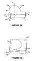
- FIGS. 6A and 6Bare side and perspective views, respectively, of an LED package according to further embodiments of the invention.
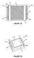
- FIGS. 7A and 7Bare bottom and perspective views, respectively, of a submount for an LED package according to further embodiments of the invention.
- FIG. 8is a plan view of a group of connected submounts prior to separation, according to some embodiments of the invention.
- FIG. 9is a plan view of a sheet of submounts according to some embodiments of the invention.
- FIGS. 10A to 10Cillustrate packaging systems/methods according to some embodiments of the invention
- FIGS. 11A to 11Cillustrate packaging systems/methods according to further embodiments of the invention.
- FIG. 12is a flowchart illustrating systems/methods according to some embodiments of the invention. It's safe
- first, second, etc.may be used herein to describe various elements, components, regions, layers and/or sections, these elements, components, regions, layers and/or sections should not be limited by these terms. These terms are only used to distinguish one element, component, region, layer or section from another region, layer or section. Thus, a first element, component, region, layer or section discussed below could be termed a second element, component, region, layer or section without departing from the teachings of the present invention.
- the term semiconductor light emitting devicemay include a light emitting diode, laser diode and/or other semiconductor device which includes one or more semiconductor layers, which may include silicon, silicon carbide, gallium nitride and/or other semiconductor materials, a substrate which may include sapphire, silicon, silicon carbide and/or other microelectronic substrates, and one or more contact layers which may include metal and/or other conductive layers.
- semiconductor layerswhich may include silicon, silicon carbide, gallium nitride and/or other semiconductor materials
- a substratewhich may include sapphire, silicon, silicon carbide and/or other microelectronic substrates
- contact layerswhich may include metal and/or other conductive layers.
- ultraviolet, blue and/or green light emitting diodes (“LEDs”)may be provided. Red and/or amber LEDs may also be provided.
- LEDsultraviolet, blue and/or green light emitting diodes
- Red and/or amber LEDsmay also be provided.
- FIGS. 2A to 2Care plan, bottom and sectional views, respectively, of a submount 30 for an LED package according to some embodiments of the invention.
- FIG. 2Cis a cross section of the submount 30 taken along line C-C of FIGS. 2A and 2B .
- a submount 30includes a generally rectangular substrate 32 having a first side 31 and a second side 33 .
- a first bondpad 36 and a second bond pad 34are formed on the first side 31 of the substrate 32 .
- the first bond pad 36includes a die attach region 36 A that is offset from a center of the substrate 32 towards a first end 32 A of the substrate 32 .
- the second bond pad 34includes a bonding region 34 A that is between the die attach region 36 A and a second end 32 B of the substrate 32 , that is opposite the first end 32 A.
- the second bond pad 34includes a second bond pad extension 34 B that extends from the bonding region 34 A along a side 32 D of the substrate 32 toward a corner 35 A of the substrate 32 at the first end 32 A of the substrate 32 .
- First and second solder pads 46 , 44are formed on the second side 33 of the substrate 32 .
- the first solder pad 46is adjacent the first end 32 A of the substrate 32
- the second solder pad 44is adjacent the second end 32 B of the substrate 32 .
- the second bond pad 34is in electrical contact with the first solder pad 46 and the first bond pad 36 is in electrical contact with the second solder pad 44 .
- the substrate 32includes a castellation 40 A at the corner 35 A of the substrate 32 .
- An electrical trace 42 A on the castellation 40 Aextends from the first surface 31 of the substrate 32 to the second surface 33 of the substrate 32 .
- the electrical trace 42electrically connects the second bond pad 34 and the first solder pad 46 .
- the first bond padfurther includes a first bond pad extension 36 B that extends from the die attach region 36 A along a second side 32 C of the substrate 32 , opposite the first side 32 D of the substrate 32 , towards a second corner 35 B of the substrate 32 at the second end 32 B of the substrate 32 and diagonally opposed to the first corner 35 A across the substrate 32 .
- the substrate 32includes a castellation 40 B at the second corner 35 B of the substrate 32 .
- a second electrical trace 42 Bis formed in the second castellation 40 B and extends from the first surface 31 of the substrate 32 to the second surface 33 of the substrate 32 .
- the second electrical trace 42 Belectrically connects the first bond pad 36 and the second solder pad 44 .
- the submount 30may include at least one via hole 38 through the substrate 32 extending from the first surface 31 of the substrate 32 to the second surface 33 of the substrate 32 .
- a conductive material, such as metal, deposited in the via hole 38electrically connects the first bond pad 36 and the second solder pad 44 , as shown in FIG. 2C .
- the substrate 32may include a nonconductive material such as alumina, aluminum nitride, silicon carbide and/or chemical vapor deposited (CVD) diamond on which a plurality of electrical traces (not shown) may be formed.
- the substrate 32may in some cases include a composite of ceramics and/or organic materials and/or metals.
- the thermal conductivity of aluminum nitride and silicon carbideis about 200 W/MK, while the thermal conductivity of CVD diamond is about 800 W/MK.
- the thickness of the substrate 32may be from about 150 to about 400 ⁇ m, although other thicknesses may be used.
- the specific heat of a materialmay be considered in selecting an appropriate material for the substrate 32 .
- a materialin some applications, such as camera flashes, it may be desirable for a material to have a high thermal capacity (thermal mass) in order to absorb a high heat flux that is generated for a very brief time, which may increase the transient temperature dissipation time constant of the package. This may particularly be desirable for applications in which an external heatsink is not provided.
- aluminamay have about 44% more thermal capacitance than AlN, alumina may be an appropriate choice of material for the substrate 32 for some applications, and in particular for applications in which an external heat sink is not provided.
- a 96% alumina substratehaving a thickness of about 340 ⁇ m and a flatness of about 0.015 mm/linear mm may be used for the substrate 32 .
- the first bond pad 36 and the second bond pad 34may include relatively thick traces for improved electrical and/or thermal conductivity.
- the first bond pad 36 and the second bond pad 34may include about 75 ⁇ m thick copper plating.
- the first bond pad 36 and the second bond pad 34may be formed by sputtering a thin seed layer of platinum or titanium/platinum onto the substrate 32 and forming a thick layer on the seed layer.
- the first bond pad 36is illustrated in partial cross section in FIG. 2D .
- the first bond pad 36includes a seed layer 36 a , an optional first barrier layer 36 b on the seed layer 36 a , and a relatively thick thermal spreading layer 36 c on the first barrier layer 36 b .
- a second barrier layer 36 dis on the thermal spreading layer 36 c
- a reflector 36 eis on the second barrier layer 36 d .
- the second bond pad 34will typically be formed at the same time as the first bond pad 36 and may have the same structure as the first bond pad 36 .
- the seed layer 36 awhich may have a thickness of about 0.006 ⁇ m, may be sputtered onto the substrate 32 and then may be patterned using standard lithographic processes to form the desired outline of the bond pads 36 , 34 .
- the optional barrier layer 36 bwhich may include about 0.2 of nickel, may then be formed on the seed layer 36 a.
- a thermal spreading layer 36 c as described abovemay then be formed on the seed layer 36 a , for example, using an electrolytic or electroless plating technique.
- the thermal spreading layer 36 cmay include a layer of copper having a thickness of about 5 ⁇ m up to hundreds of microns thick, and in some cases may be about 75 ⁇ m thick.
- the thickness of the thermal spreading layer 36 cwill influence the heat transfer properties of the package.
- a thicker thermal spreading layer 36 cmay preferentially spread heat laterally, while a thinner thermal spreading layer 36 c may preferentially spread heat vertically.
- a thinner thermal spreading layer 36 cmay be used with a substrate 32 having a larger thermal conductivity for vertical heat spreading.
- a clean-up etchsuch as a wet copper etch, may be performed to remove any material undesirably bridging between the bond pads 36 , 34 .
- the second barrier layer 36 dwhich may include nickel, may then be formed on the thermal spreading layer 36 c .
- the second barrier layer 36 dmay have a thickness of about 0.2 ⁇ m to about 2 ⁇ m.
- the reflective layer 36 emay be formed on the second barrier layer 36 d .
- the reflective layer 36 emay include silver having a thickness of 2 ⁇ m or more, and may improve light extraction.
- a bonding layer(not shown), such as a layer of gold, may also be provided on the reflective layer 36 e and/or the barrier layer 36 d.
- the thick thermal spreading layer 36 cmay provide improved heat spreading/extraction for the package. Furthermore, the thick thermal spreading layer 36 may enable heat to be quickly diffused into the core of the substrate 32 . Once heat flux is diffused into the substrate 32 , it may be extracted into an external heatsink, such as an MCPCB and/or heatsink fins, via a thermal joint. Heat may also be extracted from the substrate through natural and/or forced convection.
- an external heatsinksuch as an MCPCB and/or heatsink fins
- the electrical traces 42 A, 42 B and/or the first and second solder pads 46 , 44may be formed in a manner similar to the bond pads 36 , 34 .
- the vias 38may be filled, for example, with copper.
- An LED chipmay be mounted onto the first bond pad 36 or the second bond pad 34 by solder joints, eutectoid joints, and/or Ag-epoxy joints.
- the first and/or second solder pad 46 , 44can be soldered or chemically bonded to external interconnects. It will be appreciated that any suitable surface of the substrate 32 can be metallized to form a terminal and/or heatsink pad for external electrical and/or heatsink interconnects to meet a particular application requirement.
- an LED package as illustrated hereinmay include a substrate 32 having a single layer of material, which may simplify manufacturing processes and/or reduce manufacturing costs compared to packages including multiple layers for electrical routing purposes.
- castellations 40 A, 40 B to located the traces 42 A, 42 Bmay free up space on the surfaces 31 , 33 of the substrate 32 that can be used, for example, for mounting chips, connecting wirebonds, or other purposes.
- the castellations 40 A, 40 Bcan also be used as electrical contacts, providing increased flexibility for mounting the package.
- FIGS. 3A and 3Bare plan and perspective views, respectively, of a submount 30 for an LED package on which an LED chip 50 has been mounted.
- the LED chip 50includes a pair of bond pads 54 and a current spreading network 56 on an upper surface thereof.
- the bond pads 54 of the LED chip 50may provide cathode ( ⁇ ) connections to the LED chip 50 , while the anode (+) connection of the LED chip may be in electrical contact with the first bonding region 36 A of the first bond pad 36 .
- the cathode of the LED chip 50is electrically connected to the bonding region 34 A of the second bond bond pad 34 by at least one wire bond connection 52 that may include, for example, a gold or aluminum wire.
- the cathode of the LED chip 50is thereby electrically connected to the first solder pad 46 on the second side of the substrate 32 , which is located adjacent the first end 32 A of the substrate. Accordingly, both the center of the LED chip 50 and the solder pad 46 corresponding to the cathode of the LED chip 50 may be offset towards the same end of the substrate 32 . This configuration may provide a desirable optical and/or electrical arrangement for the resulting package.
- a substrate 32may have a surface area that is only about 2-3 times the size of the LED chip 50 mounted thereon, to provide a truly chip-scale package.
- FIGS. 4A to 4Care side, top perspective and bottom perspective views, respectively, of an LED package 100 according to some embodiments of the invention.
- an encapsulant 60is formed over the first surface 31 of the substrate 32 to provide mechanical and/or environmental protection for the LED chip 50 , as well as the first and second bond pads 36 , 36 and the wire bond connections 52 .
- the finished packagemay have a three-dimensional solid body. While a rectangular body is illustrated in FIGS. 4A to 4C , the package body may have a rectangular, square, semihemispheric, parabolic or other regular and/or irregular shape.
- the encapsulant 60may be optically transparent and/or may provide an appropriate index of refraction to match the chip 50 encapsulated therein and/or to provide a transition to an external index of refraction in order to increase light extraction from the package.
- Additives such as wavelength conversion materials (e.g. phosphors) and/or disperserscan be added to the encapsulant 60 .
- a wavelength conversion materialsuch as a phosphors embedded in an optical medium such as a silicone gel can be coated onto the chip 50 before formation of the encapsulant 60 .
- FIGS. 5A and 5Bare plan and top perspective views, respectively, of a submount 130 for an LED package according to further embodiments of the invention.
- the substrate 32may include generally semi-circular castellations 40 C, 40 D at opposite corners thereof.
- an electrostatic discharge (ESD) protection chip 62may be mounted in parallel with the LED 50 to provide ESD protection to the LED chip 50 .
- the ESD protection chipis mounted on the first bond pad 36 along with the LED chip 50 .
- the ESD chip 62may be mounted on the first bond pad extension 36 B.
- a wire bond connection 64connects the ESD protection chip 62 to the second bond pad 34 .
- FIGS. 6A and 6Bare side and perspective views, respectively, of an LED package 200 according to further embodiments of the invention.
- the LED package 200includes an encapsulant 60 on the first side of the substrate 32 .
- the encapsulant 60includes an optical element, such as an integrated lens portion 60 A that is offset from a center of the substrate 32 towards the first end 32 A of the substrate.
- an optical axis 70 of the lens portion 60 Amay be vertically aligned with a center of the LED chip 50 , which is also offset towards the first end 32 A of the substrate 32 .
- An optical element, such as the lens portion 60 A, that is integral with the encapsulant body 60may improve the luminous efficiency of the package and/or may provide a desired radiation pattern for the packaged device.
- the optical center of the packagemay be placed in any desired location, including the geometrical center of the package.
- the bond pads 36 , 34may be modified from the configurations illustrated herein in order to achieve a package having a desired shape.
- additional optical elementsmay be added to the package 100 after formation thereof.
- a secondary optical elementsuch as a lens, reflector and/or other imaging or non-imaging component can be bonded to the encapsulant 60 using a refractive index-matching adhesive.
- FIGS. 7A and 7Bare bottom and perspective views, respectively, of a submount 230 for an LED package according to further embodiments of the invention.
- the submount 230includes a neutral pad 48 on the second surface 33 of the substrate 32 between the first solder pad 46 and the second solder pad 44 .
- the neutral pad 48is electrically isolated from the first solder pad 46 and the second solder pad 44 , and may be used to provide a thermal connection between the submount 230 and a surface on which the submount 230 is mounted.
- the neutral pad 48may have the same material composition as the first and second solder pads 46 , 44 (which, in turn, may be formed in the manner described above with respect to the first and second bond pads 36 , 34 ).
- FIG. 8is a plan view of a rectangular piece 72 including a group of four connected substrates 32 - 1 to 32 - 4 prior to separation thereof.
- the group of substrates 32 - 1 to 32 - 4are defined by forming a square castellation hole 140 B at a center of the rectangular piece 72 , which forms the second castellation 40 B for each of the substrates 32 - 1 to 32 - 4 .
- Square castellation holes 140 Aare formed at the corners of the rectangular piece 72 , and provide the first castellations 40 A for each of the substrates 32 - 1 to 32 - 4 . Since a single square castellation hole 140 B forms four castellations 40 B (i.e. one for each of the substrates 32 - 1 to 32 - 4 ), when the substrates 32 - 1 to 32 - 4 are separated along horizontal and vertical separation lines 75 , 77 , the size of the castellations 40 B may be reduced.
- FIG. 9is a plan view of a sheet 74 of rectangular pieces 72 , each of which may include four substrates 32 - 1 to 32 - 4 , according to some embodiments of the invention. Accordingly, the substrates 32 may be fabricated in large numbers by patterning and metallizing many substrates 32 at once.
- FIG. 9also illustrates castellation holes 140 B at the centers of the pieces 72 and castellation holes 140 A arranged at corners of the pieces.
- the sheet 74may also include alignment features 73 , such as 1 ⁇ 4 circle holes at corners thereof and a 1 ⁇ 2 circle hole at an edge thereof, which may be used to align the sheet 74 in manufacturing processes from die attach through encapsulation and sawing.
- FIGS. 10A to 10Cillustrate packaging systems/methods according to some embodiments of the invention.
- a mold 80 including a plurality of mold cavities 81is provided.
- the mold cavities 81are separated by sidewalls 82 and are arranged to correspond to individual submounts 30 in a sheet 74 of metallized submounts 30 on which LED chips 50 have been mounted.
- a liquid casting material 68such as a clear liquid thermoset material, is dispensed into the cavities 81 , and the sheet 74 is brought into contact with the mold 80 so that the LED chips 50 extend into the mold cavities 81 and become covered with the casting material 68 .
- the casting material 68is then at least partially cured, for example by heating.
- the sheet 72is separated from the mold 80 , as shown in FIG. 10B , leaving solidified encapsulant coatings 60 on the LED chips 50 .
- the submounts 30may then be separated from one another, as shown in FIG. 10C , to form singulated packaged LEDs 100 .
- the submounts 30may be separated by sawing through the sheet 74 through the holes 140 B, 140 A, to leave castellations 40 A, 40 B in the corners of the substrates 32 .
- CTEcoefficient of thermal expansion
- FIGS. 11A to 11Cillustrate packaging systems/methods according to further embodiments of the invention.
- a mold 90 including a plurality of individual mold cavities 91is provided.
- the individual mold cavities 91are separated by sidewalls 92 and are arranged to correspond to individual submounts 30 in a sheet 74 of metallized submounts 30 on which LED chips 50 have been mounted.
- each mold cavity 91includes a lens molding surface 94 that is shaped to mold the casting material 68 into a desired lens shape at a desired location on the substrate 32 .
- the encapsulant 60when the encapsulant 60 is formed, it includes an integral lens portion 60 A corresponding to the lens molding surface 94 .
- FIG. 12is a flowchart illustrating systems/methods according to some embodiments of the invention.
- a panel of substrate materialsuch as a panel of alumina and/or AlN is provided.
- a plurality of castellation holes 140 B, and optionally, via holes 38may be formed in the panel, for example, by etching (Block 510 ).
- the panelis then metallized to form bond pads, solder pads, and conductive vias in the via holes 38 and/or the castellation holes 140 B (Block 520 ).
- a plurality of LED chipsare then mounted on respective bond pads on the panel (Block 530 ).
- a plurality of ESD protection chipsmay also be mounted on corresponding bond pads. Wire bonds may then be formed from the chips to corresponding bond pads (Block 540 ).
- An encapsulant materialsuch as a thermoset, may then be cast over the chips (Block 550 ).
- a mold including individual mold cavitiesmay be at least partially filled with a liquid encapsulant material, and the panel may be placed in contact with the mold, so that the chips on the panel extend into the mold cavities.
- the moldmay be pressurized, and may be at least partially cured before separating the panel from the mold.
- thermosetthat may be used according to some embodiments of the invention may include an epoxy, polyimide, a phenolic resin and/or any other thermosettable material.
- a thermoset for use in some embodiments of the inventioncan be transfer molded onto a leadframe, such as a stamped or etched dual-gauge leadframe. Other types of molding may be used to form a body on a leadframe, such as injection molding and/or casting.
- thermosetWhen the thermoset is chemically cross-linked (i.e., cured), it will chemically bond to the substrate to form a robust 3-dimensional solid thermoset body.
- thermoset bodymay offer enhanced structural and/or environmental protection to the device(s) mounted in the package compared to other types of materials.
- thermosetting plasticsare polymer materials that may be dispensed in precursor form, such as a resin, and then cured to a stronger form through the addition of energy, such as heat (generally near 200° C.) or irradiation.
- the curing processtransforms the resin into a solid plastic by a cross-linking process in which the molecular chains of the material react at chemically active sites and link into a rigid, three-dimensional structure.
- the cross-linking processforms a molecule with a larger molecular weight, resulting in a material with a higher melting point or that simply changes to carbon and residue without melting.
- a thermoset materialmay not be melted and re-shaped after it is cured.
- thermoset materialsare generally stronger than thermoplastic materials.
- thermoset materialsmay be better suited for high-temperature applications than thermoplastic materials.
- thermosetssuch as epoxy and/or polyimide
- This bond at the surfacemay be very strong and/or may be impervious to fluids or gases, such that a soft-gel encapsulant surrounding the semiconductor device(s) mounted in the package may not leak out.
- the bond between the thermoset and the leadframemay reduce or prevent the entry of moisture into the package, which could otherwise cause device failure.
- thermosetssuch as epoxy or phenolic resin may be found in the bonding and sealing properties of thermosets at the interface with an organic and/or inorganic surface on which it is molded. This bonding may reduce and/or prevent moisture and/or other fluids or gases from passing through the interface.
- a thermosetmay provide a higher degree of hermeticity at the interface than a thermal plastic can offer.
- thermosetscan withstand temperatures in excess of 350° C. without becoming deformed or distorted.
- thermosetsmay be able to withstand higher temperatures than conventional thermoplastic materials, such as PPA (e.g., Amodel®) and/or LCP (e.g., Vectra®), each of which can only withstand temperatures up to about 280° C. Accordingly, most thermal plastic materials cannot withstand the high solder reflow temperatures typically used for surface mount technology, which may be used to mount some LED packages.
- Thermosetssuch as many epoxies, can be molded by transfer molding, compression molding and/or casting processes to create plastic bodies having very fine details and/or intricate designs.
- a thermosetmay typically first transform into a flowable state before it is cured into a solid state.
- high pressurecan be applied to the material to allow the fluidic resin to fill even very small crevices in a mold.
- a thermal plasticmay not be able to fill spaces as small as a thermoset can, because the injection mold for a thermal plastic is typically set at a temperature below the melting temperature of the thermal plastic, which may start to cool the thermal plastic to a solid state as soon as it enters the mold cavity.
- thermoset materialsare epoxy resins and phenol-novolac resins from Nitto Denko. Such materials may be loaded with filler particles, such as spherical fused silica and/or irregularly-shaped TiO 2 (titanium dioxide) solid particles, and/or carbon fibers at predetermined percentage by weight in order to obtain desired physical properties, such as coefficient of thermal expansion (CTE), flexural modulus, optical surface reflectance, heat deflection temperature (HDT), etc.
- CTEcoefficient of thermal expansion
- flexural modulusflexural modulus
- HDTheat deflection temperature
- thermoset resinin solid or liquid form, is then loaded or dispensed into the mold cavity, which is set at a high temperature (typically at about 175° C.). Pressure (hundreds of psia) is applied to the thermoset resin to push the resin into the runner system of the mold. At this time, the solid resin will melt into a solution of very low viscosity. The liquid resin may then flow easily through the mold runners into the mold cavities, filling small crevices and corners. The pressure on the mold is increased to about 1,000 psia to pack the resin into the smallest gaps in the mold.
- the liquid thermosetis continuously subjected to the high mold temperature of about 175° C. or more and a high material pressure of about 1,000 psia. Under these conditions, the liquid thermoset will solidify/cure in about 3-5 minutes.
- a thermoset curesa cross-linking process occurs in which its constituent monomers or polymers chemically react with one another to form large, three-dimensional molecules that give solid thermoset material rigidity and a high melting point.
- the cross-linking actionalso causes the thermoset to chemically adhere or bond to the dual-gauge leadframe, imparting high mechanical stability to the resulting body/leadframe structure as well as providing a tight seal to the leadframe. This phenomenon of bonding may be desirable for a package for a semiconductor light emitting diode, in that an encapsulant can then be contained and retained inside without leaking out from the package.
- the mold cavitymay be made of hardened mold steel and polished to a mirror finish to reduce the tendency of the hardened thermoset to bond to the mold cavity.
- strong ejectorsmay be used to eject the molded panel from the mold.
- the moldmay have a Teflon® coating to promote separation and/or a mold release material may be provided in the cavities 81 , 91 to promote separation.
- the packaged chipsmay be separated from the panel (Block 560 ) to provide individual chip-scale packaged diodes.
- Packaged light emitting diodesmay provide improved luminous flux per unit area, due in part to the chip-scale size of the package footprint.
- a package according to some embodiments of the invention that includes a model EZXT-1000 LED power chip manufactured by Cree, Inc., operating at 350 mA and 100% duty cyclecan deliver about 26 lumens/mm 2 or more.
- Such a packagemay be particularly useful in applications in which a small, lightweight package is desirable, such as portable security lights, camera flashes, and/or backlighting for portable electronic devices.
- some embodimentsmay be mounted together in a cluster to provide a high-intensity light source in applications such as automotive headlamps, brake lamps, traffic lamps, etc.
- Providing package-level optical elements, such as the lens 60 Amay also ease the design and/or manufacture of secondary optical elements in systems using packages according to embodiments of the invention.
Landscapes
- Engineering & Computer Science (AREA)
- Computer Hardware Design (AREA)
- Microelectronics & Electronic Packaging (AREA)
- Power Engineering (AREA)
- Led Device Packages (AREA)
Abstract
Description
- This invention relates to semiconductor light emitting devices, and more particularly to packages for semiconductor light emitting devices.
- Light emitting diodes and laser diodes are well known solid state electronic devices capable of generating light upon application of a sufficient voltage. Light emitting diodes and laser diodes may be generally referred to as light emitting devices (LEDs). Light emitting devices generally include a p-n junction formed in an epitaxial layer grown on a substrate such as sapphire, silicon, silicon carbide, gallium arsenide and the like. The wavelength distribution of the light generated by the LED depends on the material from which the p-n junction is fabricated and the structure of the thin epitaxial layers that include the active region of the device.
- Typically, an LED includes a substrate, an n-type epitaxial region formed on the substrate and a p-type epitaxial region formed on the n-type epitaxial region (or vice-versa). In order to facilitate the application of a voltage to the device, an anode ohmic contact is formed on a p-type region of the device (typically, an exposed p-type epitaxial layer) and a cathode ohmic contact is formed on an n-type region of the device (such as the substrate or an exposed n-type epitaxial layer).
- In order to use an LED in a circuit, it is desirable to package the LED to protect it from environmental harm and mechanical damage. An LED package also includes means, such as electrical leads, for electrically connecting the LED chip to an external circuit. In a
typical package 10 illustrated inFIG. 1A , anLED 12 is mounted on areflective cup 13 by means of a solder bond or epoxy. One or more wirebonds connect the ohmic contacts of the LED to leads15A,15B which may be attached to or integral with thereflective cup 13. The entire assembly is then encapsulated in a clearprotective resin 14 which may be molded in the shape of a lens to collimate the light emitted from theLED chip 12. - In another
conventional package 20 illustrated inFIG. 1B , a plurality ofLED chips 22 are mounted onto a printed circuit board (PCB)carrier 23. One or more wirebond connections are made between ohmic contacts on theLEDs 22 andelectrical traces PCB 23. Each mountedLED 22 is then covered with a drop ofclear resin 24 which may provide environmental and mechanical protection to the chip while also acting as a lens. The individual packagedLEDs 22 are then separated by sawing thePCB board 23 into small squares, each of which contains one ormore LED chips 22. - One figure of merit for users of light emitting devices is cost per lumen, that is, the cost of obtaining a given level of light output. The high cost of conventional packaging techniques may be one factor that keeps the cost per lumen of solid state lighting relatively high. In addition, conventional packaging techniques may result in large, bulky packages that are unsuitable for certain miniaturized applications such as cellular telephone backlights. Conventional packaging techniques may also have poor thermal resistance characteristics that limit the power levels at which the LED chip may be driven and place constraints on system designers with respect to placement of LEDs.
- Some packages for light emitting diodes are described in U.S. Pre-grant Publication Nos. 2004/0079957, 2004/0126913, and 2005/0269587 which are assigned to the assignee of the present invention, and which are incorporated herein by reference as if set forth fully herein.
- Some embodiments of the invention provide a submount for a light emitting device package. The submount includes a generally rectangular substrate having a first surface and a second surface opposite the first surface, a first end and a second end opposite the first end. A first bond pad and a second bond pad are on the first surface of the substrate. The first bond pad may include a die attach region offset toward the first end of the substrate and configured to receive a light emitting diode thereon. The second bond pad may include a bonding region that is between the first bond pad and the second end of the substrate and a second bond pad extension that extends from the bonding region along a side of the substrate toward a corner of the substrate at the first end of the substrate.
- The substrate further includes first and second solder pads on the second surface of the substrate. The first solder pad is adjacent the first end of the substrate and the second solder pad is adjacent the second end of the substrate. The second bond pad is in electrical contact with the first solder pad, and the first bond pad is in electrical contact with the second solder pad.
- The substrate may include a castellation at the corner of the substrate and an electrical trace on the castellation that extends from the first surface of the substrate to the second surface of the substrate and that electrically connects the second bond pad and the first solder pad.
- The side of the substrate may include a first side and the corner of the substrate may include a first corner, and the first bond pad may further include a first bond pad extension that extends from the die attach region along a second side of the substrate, opposite the first side of the substrate, towards a second corner of the substrate at the second end of the substrate and diagonally opposed to the first corner.
- The substrate may include a castellation at the second corner of the substrate. A second electrical trace may be on the second castellation and may extend from the first surface of the substrate to the second surface of the substrate to electrically connect the first bond pad and the second solder pad.
- The submount may further include a neutral pad on the second surface of the substrate between the first solder pad and the second solder pad. The neutral pad may be electrically isolated from the first solder pad and the second solder pad.
- The substrate may include an electrically insulating material, such as aluminum nitride, silicon carbide, diamond, and/or alumina.
- The submount may further include at least one via hole through the substrate extending from the first surface of the substrate to the second surface of the substrate. A conductive material may be in the at least one via hole and may electrically connect the first bond pad and the second solder pad.
- The first bond pad may include a seed layer on the substrate and a thermal spreading layer on the seed layer. The thermal spreading layer may include a layer of copper having a thickness greater than about 5 μm.
- The first bond pad may further include a barrier layer on the thermal spreading layer opposite the seed layer, and a reflective layer on the barrier layer opposite the thermal spreading layer. The first bond pad may further include second barrier layer between the seed layer and the thermal spreading layer.
- A light emitting device package according to some embodiments of the invention includes a generally rectangular substrate having a first surface and a second surface opposite the first surface, a first end and a second end opposite the first end, and, a first bond pad on the first surface of the substrate. The first bond pad may include a die attach region offset from a center of the first surface toward the first end of the substrate and configured to receive a light emitting diode thereon. The substrate may further include a second bond pad on the first surface of the substrate including a bonding region that is between the first bond pad and the second end of the substrate, and a second bond pad extension that extends from the bonding region along a side of the substrate toward a corner of the substrate at the first end of the substrate.
- The substrate further includes first and second solder pads on the second surface of the substrate. The first solder pad is adjacent the first end of the substrate and the second solder pad is adjacent the second end of the substrate. The second bond pad is in electrical contact with the first solder pad, and the first bond pad is in electrical contact with the second solder pad.
- A light emitting device having an electrical contact is mounted on the first bond pad, and a bond wire is bonded to the electrical contact of the light emitting device and to the second bond pad.
- An encapsulant may be on the first surface of the substrate. The encapsulant may include an integrated lens arranged over the light emitting device. The integrated lens may have an optical axis that is aligned over a center of the light emitting device, so that the integrated lens is offset from a center of the substrate toward the first end of the substrate.
- The package may further include an ESD protection chip including an electrical contact, the ESD protection chip mounted on the first bond pad, and a second bond wire electrically connecting the electrical contact of the ESD protection chip and the second bond pad.
- The encapsulant may include a wavelength conversion material and/or a disperser. In some embodiments, the package may include a wavelength conversion material between the light emitting device and the encapsulant. The package may further include a secondary optical element on the encapsulant.
- Some embodiments of the invention provide methods of forming a submount for a light emitting diode (LED) package. The methods include providing a generally rectangular substrate having a first surface and a second surface opposite the first surface, a first end and a second end opposite the first end, a first corner at the first end and a second corner at the second end and diagonally across the substrate from the first corner. A seed layer is formed on the first surface of the substrate, and is patterned to form a first bond pad pattern and a second bond pad pattern on the first surface of the substrate.
- A first bond pad is formed on the first bond pad pattern. The first bond pad may include a die attach region offset from a center of the first surface toward the first end of the substrate and configured to receive a light emitting diode thereon. A second bond pad is formed on the second bond pad pattern. The second bond pad may include a bonding region that is between the first bond pad and the second end of the substrate and a second bond pad extension that extends from the bonding region along a side of the substrate toward a corner of the substrate at the first end of the substrate. The methods further include etching the first bond pad and the second bond pad to increase a separation between the first bond pad and the second bond pad.
- The methods may further include forming first and second solder pads on the second surface of the substrate. The first solder pad may be formed adjacent the first end of the substrate and the second solder pad may be formed adjacent the second end of the substrate. The second bond pad may be in electrical contact with the first solder pad and the first bond pad may be in electrical contact with the second solder pad.
- The methods may further include removing material from the first corner and the second corner to provide respective first and second castellations at the first corner and the second corner. A first electrical via may be formed on the first castellation to electrically connect the second bond pad and the first solder pad. A second electrical via may be formed on the second castellation to electrically connect the first bond pad and the second solder pad.
- Some embodiments of the invention provide methods of forming a plurality of packaged light emitting diodes. The methods include providing a sheet of ceramic material including a two-dimensional array of light emitting devices mounted thereon, providing a mold including a plurality of cavities therein, dispensing a liquid encapsulant material into respective ones of the plurality of cavities, and bringing the sheet of ceramic material into contact with the mold so that respective ones of the light emitting devices extend into a corresponding one of the plurality of cavities. The liquid encapsulant is at least partially cured so as to form encapsulant coatings around the respective light emitting devices.
- The sheet of ceramic material may include a plurality of metallized holes therethrough, and the methods may further include separating the sheet of ceramic material along separation lines that extend through a subset of the plurality of holes to thereby define individual light emitting diode substrates including at least one castellation at a corner thereof including an electrical via thereon extending from a first surface of a substrate to a second surface of the substrate.
- The accompanying drawings, which are included to provide a further understanding of the invention and are incorporated in and constitute a part of this application, illustrate certain embodiment(s) of the invention. In the drawings:
FIGS. 1A and 1B illustrate some conventional packaged light emitting devices (LEDs).FIGS. 2A to 2C are plan, bottom and sectional views, respectively, of a submount for an LED package according to some embodiments of the invention;FIG. 2D is a partial cross section of a substrate including a metal stack according to some embodiments of the invention.FIGS. 3A and 3B are plan and perspective views, respectively, of a submount for an LED package on which an LED chip has been mounted, according to some embodiments of the invention; andFIGS. 4A to 4C are side, top perspective and bottom perspective views, respectively, of an LED package according to some embodiments of the invention;FIGS. 5A to 5C are plan, top perspective and bottom perspective views, respectively, of a submount for an LED package on which an LED chip has been mounted, according to further embodiments of the invention;FIGS. 6A and 6B are side and perspective views, respectively, of an LED package according to further embodiments of the invention;FIGS. 7A and 7B are bottom and perspective views, respectively, of a submount for an LED package according to further embodiments of the invention;FIG. 8 is a plan view of a group of connected submounts prior to separation, according to some embodiments of the invention;FIG. 9 is a plan view of a sheet of submounts according to some embodiments of the invention;FIGS. 10A to 10C illustrate packaging systems/methods according to some embodiments of the invention;FIGS. 11A to 11C illustrate packaging systems/methods according to further embodiments of the invention;FIG. 12 is a flowchart illustrating systems/methods according to some embodiments of the invention. It's safe- The present invention now will be described more fully hereinafter with reference to the accompanying drawings, in which embodiments of the invention are shown. This invention may, however, be embodied in many different forms and should not be construed as limited to the embodiments set forth herein. Rather, these embodiments are provided so that this disclosure will be thorough and complete, and will fully convey the scope of the invention to those skilled in the art. In the drawings, the size and relative sizes of layers and regions may be exaggerated for clarity. Like numbers refer to like elements throughout.
- It will be understood that when an element such as a layer, region or substrate is referred to as being “on” another element, it can be directly on the other element or intervening elements may also be present. It will be understood that if part of an element, such as a surface, is referred to as “inner,” it is farther from the outside of the device than other parts of the element. Furthermore, relative terms such as “beneath” or “overlies” may be used herein to describe a relationship of one layer or region to another layer or region relative to a substrate or base layer as illustrated in the figures. It will be understood that these terms are intended to encompass different orientations of the device in addition to the orientation depicted in the figures. Finally, the term “directly” means that there are no intervening elements. As used herein, the term “and/or” includes any and all combinations of one or more of the associated listed items.
- It will be understood that, although the terms first, second, etc. may be used herein to describe various elements, components, regions, layers and/or sections, these elements, components, regions, layers and/or sections should not be limited by these terms. These terms are only used to distinguish one element, component, region, layer or section from another region, layer or section. Thus, a first element, component, region, layer or section discussed below could be termed a second element, component, region, layer or section without departing from the teachings of the present invention.
- As used herein, the term semiconductor light emitting device may include a light emitting diode, laser diode and/or other semiconductor device which includes one or more semiconductor layers, which may include silicon, silicon carbide, gallium nitride and/or other semiconductor materials, a substrate which may include sapphire, silicon, silicon carbide and/or other microelectronic substrates, and one or more contact layers which may include metal and/or other conductive layers. In some embodiments, ultraviolet, blue and/or green light emitting diodes (“LEDs”) may be provided. Red and/or amber LEDs may also be provided. The design and fabrication of semiconductor light emitting devices are well known to those having skill in the art and need not be described in detail herein.
FIGS. 2A to 2C are plan, bottom and sectional views, respectively, of asubmount 30 for an LED package according to some embodiments of the invention. In particular,FIG. 2C is a cross section of thesubmount 30 taken along line C-C ofFIGS. 2A and 2B .- Referring to
FIGS. 2A to 2C , asubmount 30 includes a generallyrectangular substrate 32 having afirst side 31 and asecond side 33. Afirst bondpad 36 and asecond bond pad 34 are formed on thefirst side 31 of thesubstrate 32. Thefirst bond pad 36 includes a die attachregion 36A that is offset from a center of thesubstrate 32 towards afirst end 32A of thesubstrate 32. Thesecond bond pad 34 includes abonding region 34A that is between the die attachregion 36A and asecond end 32B of thesubstrate 32, that is opposite thefirst end 32A. - The
second bond pad 34 includes a secondbond pad extension 34B that extends from thebonding region 34A along aside 32D of thesubstrate 32 toward acorner 35A of thesubstrate 32 at thefirst end 32A of thesubstrate 32. - First and
second solder pads second side 33 of thesubstrate 32. Thefirst solder pad 46 is adjacent thefirst end 32A of thesubstrate 32, and thesecond solder pad 44 is adjacent thesecond end 32B of thesubstrate 32. Thesecond bond pad 34 is in electrical contact with thefirst solder pad 46 and thefirst bond pad 36 is in electrical contact with thesecond solder pad 44. - The
substrate 32 includes acastellation 40A at thecorner 35A of thesubstrate 32. Anelectrical trace 42A on thecastellation 40A extends from thefirst surface 31 of thesubstrate 32 to thesecond surface 33 of thesubstrate 32. Theelectrical trace 42 electrically connects thesecond bond pad 34 and thefirst solder pad 46. - The first bond pad further includes a first
bond pad extension 36B that extends from the die attachregion 36A along asecond side 32C of thesubstrate 32, opposite thefirst side 32D of thesubstrate 32, towards asecond corner 35B of thesubstrate 32 at thesecond end 32B of thesubstrate 32 and diagonally opposed to thefirst corner 35A across thesubstrate 32. - The
substrate 32 includes acastellation 40B at thesecond corner 35B of thesubstrate 32. A second electrical trace42B is formed in thesecond castellation 40B and extends from thefirst surface 31 of thesubstrate 32 to thesecond surface 33 of thesubstrate 32. The second electrical trace42B electrically connects thefirst bond pad 36 and thesecond solder pad 44. - In some embodiments, the
submount 30 may include at least one viahole 38 through thesubstrate 32 extending from thefirst surface 31 of thesubstrate 32 to thesecond surface 33 of thesubstrate 32. A conductive material, such as metal, deposited in the viahole 38 electrically connects thefirst bond pad 36 and thesecond solder pad 44, as shown inFIG. 2C . - The
substrate 32 may include a nonconductive material such as alumina, aluminum nitride, silicon carbide and/or chemical vapor deposited (CVD) diamond on which a plurality of electrical traces (not shown) may be formed. Thesubstrate 32 may in some cases include a composite of ceramics and/or organic materials and/or metals. The thermal conductivity of aluminum nitride and silicon carbide is about 200 W/MK, while the thermal conductivity of CVD diamond is about 800 W/MK. The thickness of thesubstrate 32 may be from about 150 to about 400 μm, although other thicknesses may be used. - In some embodiments, the specific heat of a material may be considered in selecting an appropriate material for the
substrate 32. For example, in some applications, such as camera flashes, it may be desirable for a material to have a high thermal capacity (thermal mass) in order to absorb a high heat flux that is generated for a very brief time, which may increase the transient temperature dissipation time constant of the package. This may particularly be desirable for applications in which an external heatsink is not provided. As alumina may have about 44% more thermal capacitance than AlN, alumina may be an appropriate choice of material for thesubstrate 32 for some applications, and in particular for applications in which an external heat sink is not provided. In some embodiments, a 96% alumina substrate having a thickness of about 340 μm and a flatness of about 0.015 mm/linear mm may be used for thesubstrate 32. - The
first bond pad 36 and thesecond bond pad 34 may include relatively thick traces for improved electrical and/or thermal conductivity. In particular, thefirst bond pad 36 and thesecond bond pad 34 may include about 75 μm thick copper plating. - In some embodiments, the
first bond pad 36 and thesecond bond pad 34 may be formed by sputtering a thin seed layer of platinum or titanium/platinum onto thesubstrate 32 and forming a thick layer on the seed layer. For example, thefirst bond pad 36 is illustrated in partial cross section inFIG. 2D . Thefirst bond pad 36 includes aseed layer 36a, an optionalfirst barrier layer 36bon theseed layer 36a, and a relatively thick thermal spreadinglayer 36con thefirst barrier layer 36b. Asecond barrier layer 36dis on the thermal spreadinglayer 36c, and areflector 36eis on thesecond barrier layer 36d. Thesecond bond pad 34 will typically be formed at the same time as thefirst bond pad 36 and may have the same structure as thefirst bond pad 36. - The
seed layer 36a, which may have a thickness of about 0.006 μm, may be sputtered onto thesubstrate 32 and then may be patterned using standard lithographic processes to form the desired outline of thebond pads optional barrier layer 36b, which may include about 0.2 of nickel, may then be formed on theseed layer 36a. - A thermal spreading
layer 36cas described above may then be formed on theseed layer 36a, for example, using an electrolytic or electroless plating technique. The thermal spreadinglayer 36cmay include a layer of copper having a thickness of about 5 μm up to hundreds of microns thick, and in some cases may be about 75 μm thick. The thickness of the thermal spreadinglayer 36cwill influence the heat transfer properties of the package. A thicker thermal spreadinglayer 36cmay preferentially spread heat laterally, while a thinner thermal spreadinglayer 36cmay preferentially spread heat vertically. Thus, a thinner thermal spreadinglayer 36cmay be used with asubstrate 32 having a larger thermal conductivity for vertical heat spreading. - A clean-up etch, such as a wet copper etch, may be performed to remove any material undesirably bridging between the
bond pads second barrier layer 36d, which may include nickel, may then be formed on the thermal spreadinglayer 36c. Thesecond barrier layer 36dmay have a thickness of about 0.2 μm to about 2 μm. Thereflective layer 36emay be formed on thesecond barrier layer 36d. Thereflective layer 36emay include silver having a thickness of 2 μm or more, and may improve light extraction. - A bonding layer (not shown), such as a layer of gold, may also be provided on the
reflective layer 36eand/or thebarrier layer 36d. - The thick thermal spreading
layer 36cmay provide improved heat spreading/extraction for the package. Furthermore, the thick thermal spreadinglayer 36 may enable heat to be quickly diffused into the core of thesubstrate 32. Once heat flux is diffused into thesubstrate 32, it may be extracted into an external heatsink, such as an MCPCB and/or heatsink fins, via a thermal joint. Heat may also be extracted from the substrate through natural and/or forced convection. - The
electrical traces 42A,42B and/or the first andsecond solder pads bond pads vias 38 may be filled, for example, with copper. - An LED chip may be mounted onto the
first bond pad 36 or thesecond bond pad 34 by solder joints, eutectoid joints, and/or Ag-epoxy joints. The first and/orsecond solder pad substrate 32 can be metallized to form a terminal and/or heatsink pad for external electrical and/or heatsink interconnects to meet a particular application requirement. - Due in part to the configuration of the
bond pads castellations vertical traces 42A,42B and thesolder pads substrate 32 having a single layer of material, which may simplify manufacturing processes and/or reduce manufacturing costs compared to packages including multiple layers for electrical routing purposes. - Furthermore, the use of
castellations traces 42A,42B may free up space on thesurfaces substrate 32 that can be used, for example, for mounting chips, connecting wirebonds, or other purposes. Thecastellations FIGS. 3A and 3B are plan and perspective views, respectively, of asubmount 30 for an LED package on which anLED chip 50 has been mounted. TheLED chip 50 includes a pair ofbond pads 54 and a current spreadingnetwork 56 on an upper surface thereof. Thebond pads 54 of theLED chip 50 may provide cathode (−) connections to theLED chip 50, while the anode (+) connection of the LED chip may be in electrical contact with thefirst bonding region 36A of thefirst bond pad 36. The cathode of theLED chip 50 is electrically connected to thebonding region 34A of the secondbond bond pad 34 by at least onewire bond connection 52 that may include, for example, a gold or aluminum wire.- The cathode of the
LED chip 50 is thereby electrically connected to thefirst solder pad 46 on the second side of thesubstrate 32, which is located adjacent thefirst end 32A of the substrate. Accordingly, both the center of theLED chip 50 and thesolder pad 46 corresponding to the cathode of theLED chip 50 may be offset towards the same end of thesubstrate 32. This configuration may provide a desirable optical and/or electrical arrangement for the resulting package. - As can be seen in
FIGS. 3A and 3B , asubstrate 32 may have a surface area that is only about 2-3 times the size of theLED chip 50 mounted thereon, to provide a truly chip-scale package. FIGS. 4A to 4C are side, top perspective and bottom perspective views, respectively, of anLED package 100 according to some embodiments of the invention. As shown inFIGS. 4A to 4C , anencapsulant 60 is formed over thefirst surface 31 of thesubstrate 32 to provide mechanical and/or environmental protection for theLED chip 50, as well as the first andsecond bond pads wire bond connections 52.- Accordingly, the finished package may have a three-dimensional solid body. While a rectangular body is illustrated in
FIGS. 4A to 4C , the package body may have a rectangular, square, semihemispheric, parabolic or other regular and/or irregular shape. - The
encapsulant 60 may be optically transparent and/or may provide an appropriate index of refraction to match thechip 50 encapsulated therein and/or to provide a transition to an external index of refraction in order to increase light extraction from the package. - Additives such as wavelength conversion materials (e.g. phosphors) and/or dispersers can be added to the
encapsulant 60. In some embodiments, a wavelength conversion material, such a phosphors embedded in an optical medium such as a silicone gel can be coated onto thechip 50 before formation of theencapsulant 60. FIGS. 5A and 5B are plan and top perspective views, respectively, of asubmount 130 for an LED package according to further embodiments of the invention. As shown therein, thesubstrate 32 may include generallysemi-circular castellations - Moreover, an electrostatic discharge (ESD)
protection chip 62 may be mounted in parallel with theLED 50 to provide ESD protection to theLED chip 50. As shown inFIGS. 5A and 5B , the ESD protection chip is mounted on thefirst bond pad 36 along with theLED chip 50. In particular, theESD chip 62 may be mounted on the firstbond pad extension 36B. Awire bond connection 64 connects theESD protection chip 62 to thesecond bond pad 34. FIGS. 6A and 6B are side and perspective views, respectively, of anLED package 200 according to further embodiments of the invention. TheLED package 200 includes anencapsulant 60 on the first side of thesubstrate 32. Theencapsulant 60 includes an optical element, such as anintegrated lens portion 60A that is offset from a center of thesubstrate 32 towards thefirst end 32A of the substrate. In particular, anoptical axis 70 of thelens portion 60A may be vertically aligned with a center of theLED chip 50, which is also offset towards thefirst end 32A of thesubstrate 32.- An optical element, such as the
lens portion 60A, that is integral with theencapsulant body 60 may improve the luminous efficiency of the package and/or may provide a desired radiation pattern for the packaged device. - As is apparent from
FIGS. 6A and 6B , the optical center of the package may be placed in any desired location, including the geometrical center of the package. Thebond pads - Furthermore, additional optical elements may be added to the
package 100 after formation thereof. For example, a secondary optical element such as a lens, reflector and/or other imaging or non-imaging component can be bonded to theencapsulant 60 using a refractive index-matching adhesive. FIGS. 7A and 7B are bottom and perspective views, respectively, of asubmount 230 for an LED package according to further embodiments of the invention. In addition to first andsecond solder pads submount 230 includes aneutral pad 48 on thesecond surface 33 of thesubstrate 32 between thefirst solder pad 46 and thesecond solder pad 44. Theneutral pad 48 is electrically isolated from thefirst solder pad 46 and thesecond solder pad 44, and may be used to provide a thermal connection between the submount230 and a surface on which thesubmount 230 is mounted. Theneutral pad 48 may have the same material composition as the first andsecond solder pads 46,44 (which, in turn, may be formed in the manner described above with respect to the first andsecond bond pads 36,34).- Some embodiments of the invention provide methods of forming submounts. In some embodiments, a sheet of a submount material, such as a sheet of ceramic material, may be patterned and metallized to form a plurality of
connected submounts 32. For example,FIG. 8 is a plan view of arectangular piece 72 including a group of four connected substrates32-1 to32-4 prior to separation thereof. The group of substrates32-1 to32-4 are defined by forming asquare castellation hole 140B at a center of therectangular piece 72, which forms thesecond castellation 40B for each of the substrates32-1 to32-4. Square castellation holes140A are formed at the corners of therectangular piece 72, and provide thefirst castellations 40A for each of the substrates32-1 to32-4. Since a singlesquare castellation hole 140B forms fourcastellations 40B (i.e. one for each of the substrates32-1 to32-4), when the substrates32-1 to32-4 are separated along horizontal andvertical separation lines castellations 40B may be reduced. FIG. 9 is a plan view of asheet 74 ofrectangular pieces 72, each of which may include four substrates32-1 to32-4, according to some embodiments of the invention. Accordingly, thesubstrates 32 may be fabricated in large numbers by patterning and metallizingmany substrates 32 at once.FIG. 9 also illustrates castellation holes140B at the centers of thepieces 72 andcastellation holes 140A arranged at corners of the pieces. When theindividual substrates 32 are separated, for example by sawing thesheet 74 alonghorizontal separation lines 75 andvertical separation lines 77, each resultingsubstrate 32 will have first andsecond castellations electrical traces 42A and42B are respectively formed. Thesheet 74 may also include alignment features73, such as ¼ circle holes at corners thereof and a ½ circle hole at an edge thereof, which may be used to align thesheet 74 in manufacturing processes from die attach through encapsulation and sawing.FIGS. 10A to 10C illustrate packaging systems/methods according to some embodiments of the invention. As shown therein, amold 80 including a plurality ofmold cavities 81 is provided. The mold cavities81 are separated by sidewalls82 and are arranged to correspond toindividual submounts 30 in asheet 74 of metallized submounts30 on which LED chips50 have been mounted. Aliquid casting material 68, such as a clear liquid thermoset material, is dispensed into thecavities 81, and thesheet 74 is brought into contact with themold 80 so that the LED chips50 extend into themold cavities 81 and become covered with the castingmaterial 68. The castingmaterial 68 is then at least partially cured, for example by heating.- After the casting material has been at least partially cured, the
sheet 72 is separated from themold 80, as shown inFIG. 10B , leaving solidifiedencapsulant coatings 60 on the LED chips50. Thesubmounts 30 may then be separated from one another, as shown inFIG. 10C , to form singulated packagedLEDs 100. In particular, thesubmounts 30 may be separated by sawing through thesheet 74 through theholes castellations substrates 32. - It may be beneficial to provide
separate cavities 81 for each LED package being cast in order to reduce the effect of differences in coefficient of thermal expansion (CTE) between the castingmaterial 68 and the material of thesubstrate sheet 74. For example, if the castingmaterial 68 were cast over anentire sheet 74, differences in CTE between the castingmaterial 68 and thesheet 74 may cause undesired cracking, warping and/or de-lamination of theencapsulant coatings 60. FIGS. 11A to 11C illustrate packaging systems/methods according to further embodiments of the invention. In the embodiments illustrated inFIGS. 11A to 11C , amold 90 including a plurality of individual mold cavities91 is provided. The individual mold cavities91 are separated by sidewalls92 and are arranged to correspond toindividual submounts 30 in asheet 74 of metallized submounts30 on which LED chips50 have been mounted. Furthermore, each mold cavity91 includes alens molding surface 94 that is shaped to mold the castingmaterial 68 into a desired lens shape at a desired location on thesubstrate 32.- As shown in
FIG. 11B , when theencapsulant 60 is formed, it includes anintegral lens portion 60A corresponding to thelens molding surface 94. FIG. 12 is a flowchart illustrating systems/methods according to some embodiments of the invention. A panel of substrate material, such as a panel of alumina and/or AlN is provided. A plurality of castellation holes140B, and optionally, viaholes 38, may be formed in the panel, for example, by etching (Block510). The panel is then metallized to form bond pads, solder pads, and conductive vias in the via holes38 and/or the castellation holes140B (Block520).- A plurality of LED chips are then mounted on respective bond pads on the panel (Block530). Optionally, a plurality of ESD protection chips may also be mounted on corresponding bond pads. Wire bonds may then be formed from the chips to corresponding bond pads (Block540).
- An encapsulant material, such as a thermoset, may then be cast over the chips (Block550). As described above, a mold including individual mold cavities may be at least partially filled with a liquid encapsulant material, and the panel may be placed in contact with the mold, so that the chips on the panel extend into the mold cavities. The mold may be pressurized, and may be at least partially cured before separating the panel from the mold.
- A thermoset that may be used according to some embodiments of the invention may include an epoxy, polyimide, a phenolic resin and/or any other thermosettable material. A thermoset for use in some embodiments of the invention can be transfer molded onto a leadframe, such as a stamped or etched dual-gauge leadframe. Other types of molding may be used to form a body on a leadframe, such as injection molding and/or casting.
- When the thermoset is chemically cross-linked (i.e., cured), it will chemically bond to the substrate to form a robust 3-dimensional solid thermoset body.
- A thermoset body may offer enhanced structural and/or environmental protection to the device(s) mounted in the package compared to other types of materials.
- Thermoset materials, such as thermosetting plastics are polymer materials that may be dispensed in precursor form, such as a resin, and then cured to a stronger form through the addition of energy, such as heat (generally near 200° C.) or irradiation. The curing process transforms the resin into a solid plastic by a cross-linking process in which the molecular chains of the material react at chemically active sites and link into a rigid, three-dimensional structure. The cross-linking process forms a molecule with a larger molecular weight, resulting in a material with a higher melting point or that simply changes to carbon and residue without melting. Thus, a thermoset material may not be melted and re-shaped after it is cured. As a result of the formation of a three-dimensional network of bonds during the cross-linking phase, thermoset materials are generally stronger than thermoplastic materials. Thus, thermoset materials may be better suited for high-temperature applications than thermoplastic materials.
- Most thermosets, such as epoxy and/or polyimide, will bond to organic and/or inorganic surfaces when they come into contact with the surface during the cross-linking (curing) phase. This bond at the surface may be very strong and/or may be impervious to fluids or gases, such that a soft-gel encapsulant surrounding the semiconductor device(s) mounted in the package may not leak out. Furthermore, the bond between the thermoset and the leadframe may reduce or prevent the entry of moisture into the package, which could otherwise cause device failure.
- In contrast, in a package including a thermoplastic molded body, there may be no bonding between the plastic body and the surface on which it is molded. As such, fluids and/or gases can pass in both directions through the interface between the thermoplastic and the leadframe. Accordingly, an advantage of using thermosets such as epoxy or phenolic resin may be found in the bonding and sealing properties of thermosets at the interface with an organic and/or inorganic surface on which it is molded. This bonding may reduce and/or prevent moisture and/or other fluids or gases from passing through the interface. Thus, a thermoset may provide a higher degree of hermeticity at the interface than a thermal plastic can offer.
- Many thermosets can withstand temperatures in excess of 350° C. without becoming deformed or distorted. In general, thermosets may be able to withstand higher temperatures than conventional thermoplastic materials, such as PPA (e.g., Amodel®) and/or LCP (e.g., Vectra®), each of which can only withstand temperatures up to about 280° C. Accordingly, most thermal plastic materials cannot withstand the high solder reflow temperatures typically used for surface mount technology, which may be used to mount some LED packages.
- Thermosets, such as many epoxies, can be molded by transfer molding, compression molding and/or casting processes to create plastic bodies having very fine details and/or intricate designs. During the molding/casting process, a thermoset may typically first transform into a flowable state before it is cured into a solid state. During this fluid state, high pressure can be applied to the material to allow the fluidic resin to fill even very small crevices in a mold. A thermal plastic may not be able to fill spaces as small as a thermoset can, because the injection mold for a thermal plastic is typically set at a temperature below the melting temperature of the thermal plastic, which may start to cool the thermal plastic to a solid state as soon as it enters the mold cavity.
- Examples of thermoset materials are epoxy resins and phenol-novolac resins from Nitto Denko. Such materials may be loaded with filler particles, such as spherical fused silica and/or irregularly-shaped TiO2(titanium dioxide) solid particles, and/or carbon fibers at predetermined percentage by weight in order to obtain desired physical properties, such as coefficient of thermal expansion (CTE), flexural modulus, optical surface reflectance, heat deflection temperature (HDT), etc.
- The thermoset resin, in solid or liquid form, is then loaded or dispensed into the mold cavity, which is set at a high temperature (typically at about 175° C.). Pressure (hundreds of psia) is applied to the thermoset resin to push the resin into the runner system of the mold. At this time, the solid resin will melt into a solution of very low viscosity. The liquid resin may then flow easily through the mold runners into the mold cavities, filling small crevices and corners. The pressure on the mold is increased to about 1,000 psia to pack the resin into the smallest gaps in the mold.
- Inside the mold cavities, the liquid thermoset is continuously subjected to the high mold temperature of about 175° C. or more and a high material pressure of about 1,000 psia. Under these conditions, the liquid thermoset will solidify/cure in about 3-5 minutes. As noted above, when a thermoset cures, a cross-linking process occurs in which its constituent monomers or polymers chemically react with one another to form large, three-dimensional molecules that give solid thermoset material rigidity and a high melting point. The cross-linking action also causes the thermoset to chemically adhere or bond to the dual-gauge leadframe, imparting high mechanical stability to the resulting body/leadframe structure as well as providing a tight seal to the leadframe. This phenomenon of bonding may be desirable for a package for a semiconductor light emitting diode, in that an encapsulant can then be contained and retained inside without leaking out from the package.
- Since the thermoset resin bonds readily to surfaces, the mold cavity may be made of hardened mold steel and polished to a mirror finish to reduce the tendency of the hardened thermoset to bond to the mold cavity. In addition, strong ejectors may be used to eject the molded panel from the mold. In some embodiments, the mold may have a Teflon® coating to promote separation and/or a mold release material may be provided in the
cavities 81,91 to promote separation. - After separation of the panel from the mold, the packaged chips may be separated from the panel (Block560) to provide individual chip-scale packaged diodes.
- Packaged light emitting diodes according to some embodiments of the invention may provide improved luminous flux per unit area, due in part to the chip-scale size of the package footprint. For example, a package according to some embodiments of the invention that includes a model EZXT-1000 LED power chip manufactured by Cree, Inc., operating at 350 mA and 100% duty cycle can deliver about 26 lumens/mm2or more. Such a package may be particularly useful in applications in which a small, lightweight package is desirable, such as portable security lights, camera flashes, and/or backlighting for portable electronic devices. Furthermore, some embodiments may be mounted together in a cluster to provide a high-intensity light source in applications such as automotive headlamps, brake lamps, traffic lamps, etc. Providing package-level optical elements, such as the
lens 60A, may also ease the design and/or manufacture of secondary optical elements in systems using packages according to embodiments of the invention. - The foregoing description is illustrative of the present invention and is not to be construed as limiting thereof. Although a few exemplary embodiments of this invention have been described, those skilled in the art will readily appreciate that many modifications are possible in the exemplary embodiments without materially departing from the novel teachings and advantages of this invention. Accordingly, all such modifications are intended to be included within the scope of this invention as defined in the claims. Therefore, it is to be understood that the foregoing is illustrative of the present invention and is not to be construed as limited to the specific embodiments disclosed, and that modifications to the disclosed embodiments, as well as other embodiments, are intended to be included within the scope of the appended claims. The invention is defined by the following claims, with equivalents of the claims to be included therein.
Claims (32)
Priority Applications (10)
| Application Number | Priority Date | Filing Date | Title |
|---|---|---|---|
| US11/788,001US7964888B2 (en) | 2007-04-18 | 2007-04-18 | Semiconductor light emitting device packages and methods |
| EP08742905.6AEP2147468B1 (en) | 2007-04-18 | 2008-04-15 | Semiconductor light emitting device packages and methods |
| CN201110302128XACN102738318A (en) | 2007-04-18 | 2008-04-15 | Semiconductor light emitting device packages and methods |
| CN2008800208799ACN101689590B (en) | 2007-04-18 | 2008-04-15 | Semiconductor light emitting device packaging and method |
| JP2010504064AJP5512509B2 (en) | 2007-04-18 | 2008-04-15 | Semiconductor light emitting device package and method |
| PCT/US2008/004849WO2008130541A2 (en) | 2007-04-18 | 2008-04-15 | Semiconductor light emitting device packages and methods |
| TW103138814ATW201507208A (en) | 2007-04-18 | 2008-04-17 | Semiconductor light emitting device package and method |
| TW97114012ATWI467795B (en) | 2007-04-18 | 2008-04-17 | Semiconductor light emitting device package and method |
| US13/164,185US8791491B2 (en) | 2007-04-18 | 2011-06-20 | Semiconductor light emitting device packages and methods |
| US14/284,940US20140256072A1 (en) | 2007-04-18 | 2014-05-22 | Semiconductor Light Emitting Device Packages and Methods |
Applications Claiming Priority (1)
| Application Number | Priority Date | Filing Date | Title |
|---|---|---|---|
| US11/788,001US7964888B2 (en) | 2007-04-18 | 2007-04-18 | Semiconductor light emitting device packages and methods |
Related Child Applications (2)
| Application Number | Title | Priority Date | Filing Date |
|---|---|---|---|
| US13/164,185DivisionUS8791491B2 (en) | 2007-04-18 | 2011-06-20 | Semiconductor light emitting device packages and methods |
| US13/164,185ContinuationUS8791491B2 (en) | 2007-04-18 | 2011-06-20 | Semiconductor light emitting device packages and methods |
Publications (2)
| Publication Number | Publication Date |
|---|---|
| US20080258168A1true US20080258168A1 (en) | 2008-10-23 |
| US7964888B2 US7964888B2 (en) | 2011-06-21 |
Family
ID=39639394
Family Applications (3)
| Application Number | Title | Priority Date | Filing Date |
|---|---|---|---|
| US11/788,001Active2028-04-13US7964888B2 (en) | 2007-04-18 | 2007-04-18 | Semiconductor light emitting device packages and methods |
| US13/164,185ActiveUS8791491B2 (en) | 2007-04-18 | 2011-06-20 | Semiconductor light emitting device packages and methods |
| US14/284,940AbandonedUS20140256072A1 (en) | 2007-04-18 | 2014-05-22 | Semiconductor Light Emitting Device Packages and Methods |
Family Applications After (2)
| Application Number | Title | Priority Date | Filing Date |
|---|---|---|---|
| US13/164,185ActiveUS8791491B2 (en) | 2007-04-18 | 2011-06-20 | Semiconductor light emitting device packages and methods |
| US14/284,940AbandonedUS20140256072A1 (en) | 2007-04-18 | 2014-05-22 | Semiconductor Light Emitting Device Packages and Methods |
Country Status (6)
| Country | Link |
|---|---|
| US (3) | US7964888B2 (en) |
| EP (1) | EP2147468B1 (en) |
| JP (1) | JP5512509B2 (en) |
| CN (2) | CN101689590B (en) |
| TW (2) | TW201507208A (en) |
| WO (1) | WO2008130541A2 (en) |
Cited By (27)
| Publication number | Priority date | Publication date | Assignee | Title |
|---|---|---|---|---|
| US20080142829A1 (en)* | 2004-03-29 | 2008-06-19 | Cree, Inc. | Semiconductor light emitting devices including flexible silicone film having a lens therein |
| US20100252851A1 (en)* | 2007-10-31 | 2010-10-07 | Cree, Inc. | Led package with increased feature sizes |
| US20100252840A1 (en)* | 2009-04-06 | 2010-10-07 | Cree, Inc. | High voltage low current surface emitting led |
| WO2011039023A1 (en)* | 2009-09-30 | 2011-04-07 | Osram Opto Semiconductors Gmbh | Optoelectronic component |
| US20110211334A1 (en)* | 2010-04-01 | 2011-09-01 | Wan Ho Kim | Light emitting device package and light unit having the same |
| US20110266571A1 (en)* | 2008-05-29 | 2011-11-03 | Osram Opto Semiconductors Gmbh | Semiconductor Arrangement |
| WO2011138712A1 (en)* | 2010-05-07 | 2011-11-10 | Koninklijke Philips Electronics N.V. | Led package with a rounded square lens |
| US20120187862A1 (en)* | 2007-10-31 | 2012-07-26 | Jeffrey Carl Britt | Light emitting die (led) packages and related methods |
| CN102832180A (en)* | 2011-06-16 | 2012-12-19 | 精材科技股份有限公司 | Chip package and method for forming the same |
| WO2013016346A1 (en)* | 2011-07-25 | 2013-01-31 | Cree, Inc. | High voltage low current surface emitting light emitting diode |
| US8476645B2 (en) | 2009-11-13 | 2013-07-02 | Uni-Light Llc | LED thermal management |
| CN103280514A (en)* | 2013-05-29 | 2013-09-04 | 华南理工大学 | Method for automatically packaging LED module |
| US8530921B2 (en) | 2009-04-06 | 2013-09-10 | Cree, Inc. | High voltage low current surface emitting LED |
| US20130313604A1 (en)* | 2011-04-13 | 2013-11-28 | Osram Opto Semiconductors Gmbh | Method for Producing a Light-Emitting Semiconductor Component and Light-Emitting Semiconductor Component |
| DE102012212320A1 (en)* | 2012-07-13 | 2014-01-16 | Osram Opto Semiconductors Gmbh | Carrier device for receiving component e.g. LED, has carrier that is arranged with molding material with receiving area for receiving the component, and anchoring structure is designed so that molding material with carrier is anchored |
| EP2613372A4 (en)* | 2010-09-03 | 2014-05-07 | Nichia Corp | LIGHT EMITTING DEVICE AND HOUSING FOR LIGHT EMITTING DEVICE |
| US20150179903A1 (en)* | 2012-06-11 | 2015-06-25 | Cree, Inc. | Led package with multiple element light source and encapsulant having curved and/or planar surfaces |
| US9093293B2 (en) | 2009-04-06 | 2015-07-28 | Cree, Inc. | High voltage low current surface emitting light emitting diode |
| US20160172559A1 (en)* | 2013-07-04 | 2016-06-16 | Osram Opto Semiconductors Gmbh | Method for Producing an Optoelectronic Device |
| WO2017009285A1 (en)* | 2015-07-15 | 2017-01-19 | Osram Opto Semiconductors Gmbh | Component and method for manufacturing components |
| US9806230B2 (en) | 2009-08-24 | 2017-10-31 | QROMIS, Inc. | Solid state lighting devices with selected thermal expansion and/or surface characteristics, and associated methods |
| US10431568B2 (en) | 2014-12-18 | 2019-10-01 | Cree, Inc. | Light emitting diodes, components and related methods |
| US10622522B2 (en) | 2014-09-05 | 2020-04-14 | Theodore Lowes | LED packages with chips having insulated surfaces |
| US10892383B2 (en) | 2007-10-31 | 2021-01-12 | Cree, Inc. | Light emitting diode package and method for fabricating same |
| US20210296296A1 (en)* | 2018-11-27 | 2021-09-23 | Samsung Electronics Co., Ltd. | Micro light source array, display device having the same, and method of manufacturing display device |
| CN114755852A (en)* | 2022-04-21 | 2022-07-15 | 南京京东方显示技术有限公司 | Backplane, backplane processing method, backlight module and display device |
| US12392458B2 (en)* | 2009-02-25 | 2025-08-19 | Rohm Co., Ltd. | LED lamp |
Families Citing this family (22)
| Publication number | Priority date | Publication date | Assignee | Title |
|---|---|---|---|---|
| KR20080089859A (en)* | 2007-04-02 | 2008-10-08 | 엘지이노텍 주식회사 | Nitride semiconductor light emitting device and manufacturing method thereof |
| US8716723B2 (en)* | 2008-08-18 | 2014-05-06 | Tsmc Solid State Lighting Ltd. | Reflective layer between light-emitting diodes |
| US9293656B2 (en)* | 2012-11-02 | 2016-03-22 | Epistar Corporation | Light emitting device |
| US8138509B2 (en)* | 2009-02-27 | 2012-03-20 | Visera Technologies Company, Limited | Light emitting device having luminescent layer with opening to exposed bond pad on light emitting die for wire bonding pad to substrate |
| JPWO2010131498A1 (en)* | 2009-05-12 | 2012-11-01 | 三菱電機株式会社 | Laser diode element |
| US8319339B2 (en)* | 2009-07-10 | 2012-11-27 | Stmicroelectronics (Tours) Sas | Surface-mounted silicon chip |
| KR101028329B1 (en)* | 2010-04-28 | 2011-04-12 | 엘지이노텍 주식회사 | Light emitting device package and its manufacturing method |
| US20120068218A1 (en)* | 2010-09-17 | 2012-03-22 | Taiwan Semiconductor Manufacturing Company, Ltd. | Thermally efficient packaging for a photonic device |
| CN102922661A (en)* | 2012-11-05 | 2013-02-13 | 苏州东山精密制造股份有限公司 | Light-emitting diode (LED) mold pressing packaging process and LED assembly |
| US9142432B2 (en) | 2013-09-13 | 2015-09-22 | Taiwan Semiconductor Manufacturing Company, Ltd. | Integrated fan-out package structures with recesses in molding compound |
| DE102014102810A1 (en)* | 2014-03-04 | 2015-09-10 | Osram Opto Semiconductors Gmbh | Production of optoelectronic components |
| US9786643B2 (en)* | 2014-07-08 | 2017-10-10 | Micron Technology, Inc. | Semiconductor devices comprising protected side surfaces and related methods |
| US9025423B1 (en) | 2014-07-14 | 2015-05-05 | HGST Netherlands B.V. | Thermally conductive features for a heat-assisted magnetic recording head |
| KR102371448B1 (en) | 2014-10-02 | 2022-03-08 | 삼성디스플레이 주식회사 | Light source and display device including the same |
| JP2016081562A (en) | 2014-10-09 | 2016-05-16 | ソニー株式会社 | Display apparatus, manufacturing method of the same, and electronic apparatus |
| JP2017135148A (en)* | 2016-01-25 | 2017-08-03 | スタンレー電気株式会社 | Semiconductor device |
| TWI626774B (en)* | 2016-06-13 | 2018-06-11 | 開發晶照明(廈門)有限公司 | Led leadframe and led package structure |
| TWI624884B (en)* | 2016-07-15 | 2018-05-21 | Grain size packaged diode element with ultra-low forward voltage and method of manufacturing the same | |
| CN106784252A (en)* | 2017-01-13 | 2017-05-31 | 深圳市纽艾迪电子科技有限公司 | A kind of LED-baseplate |
| CN110504231B (en)* | 2019-09-18 | 2021-03-02 | 北京大学东莞光电研究院 | A kind of preparation method of semiconductor power device |
| CN111697117B (en)* | 2020-06-23 | 2021-08-20 | 深圳市聚飞光电股份有限公司 | Chip-scale packaging method and LED packaging device |
| WO2025080367A1 (en)* | 2023-10-13 | 2025-04-17 | Lumileds Llc | Diagonal footprint design enabling close packed led arrays |
Citations (16)
| Publication number | Priority date | Publication date | Assignee | Title |
|---|---|---|---|---|
| US4843280A (en)* | 1988-01-15 | 1989-06-27 | Siemens Corporate Research & Support, Inc. | A modular surface mount component for an electrical device or led's |
| US5998925A (en)* | 1996-07-29 | 1999-12-07 | Nichia Kagaku Kogyo Kabushiki Kaisha | Light emitting device having a nitride compound semiconductor and a phosphor containing a garnet fluorescent material |
| US6204523B1 (en)* | 1998-11-06 | 2001-03-20 | Lumileds Lighting, U.S., Llc | High stability optical encapsulation and packaging for light-emitting diodes in the green, blue, and near UV range |
| US6297598B1 (en)* | 2001-02-20 | 2001-10-02 | Harvatek Corp. | Single-side mounted light emitting diode module |
| US20010042858A1 (en)* | 2000-05-18 | 2001-11-22 | Hiroki Ishinaga | Backside light emitting chip type light emitting element and insulating substrate therefor |
| US6518600B1 (en)* | 2000-11-17 | 2003-02-11 | General Electric Company | Dual encapsulation for an LED |
| US6521916B2 (en)* | 1999-03-15 | 2003-02-18 | Gentex Corporation | Radiation emitter device having an encapsulant with different zones of thermal conductivity |
| US20040041222A1 (en)* | 2002-09-04 | 2004-03-04 | Loh Ban P. | Power surface mount light emitting die package |
| US20040079957A1 (en)* | 2002-09-04 | 2004-04-29 | Andrews Peter Scott | Power surface mount light emitting die package |
| US20040126913A1 (en)* | 2002-12-06 | 2004-07-01 | Loh Ban P. | Composite leadframe LED package and method of making the same |
| US20040188851A1 (en)* | 2003-03-26 | 2004-09-30 | Nec Electronics Corporation | Semiconductor device and method for manufacturing same |
| US20050167679A1 (en)* | 2002-04-30 | 2005-08-04 | Takashi Ishii | Submount and semiconductor device |
| US20050269587A1 (en)* | 2004-06-04 | 2005-12-08 | Loh Ban P | Power light emitting die package with reflecting lens and the method of making the same |
| US20050270666A1 (en)* | 2004-06-04 | 2005-12-08 | Loh Ban P | Composite optical lens with an integrated reflector |
| US20060292747A1 (en)* | 2005-06-27 | 2006-12-28 | Loh Ban P | Top-surface-mount power light emitter with integral heat sink |
| US7355284B2 (en)* | 2004-03-29 | 2008-04-08 | Cree, Inc. | Semiconductor light emitting devices including flexible film having therein an optical element |
Family Cites Families (14)
| Publication number | Priority date | Publication date | Assignee | Title |
|---|---|---|---|---|
| US3926746A (en)* | 1973-10-04 | 1975-12-16 | Minnesota Mining & Mfg | Electrical interconnection for metallized ceramic arrays |
| JP2787388B2 (en)* | 1992-03-06 | 1998-08-13 | シャープ株式会社 | Light emitting device lens molding method |
| JPH07131072A (en)* | 1993-10-29 | 1995-05-19 | Rohm Co Ltd | Surface-mount type side face light emitting equipment, light emitting device using it, and liquid crystal display using light emitting device |
| US6274890B1 (en)* | 1997-01-15 | 2001-08-14 | Kabushiki Kaisha Toshiba | Semiconductor light emitting device and its manufacturing method |
| DE29825022U1 (en) | 1997-07-29 | 2004-04-01 | Osram Opto Semiconductors Gmbh | Optoelectronic component |
| ES2142281B1 (en) | 1998-06-05 | 2000-12-01 | Fernandez Angel Alberto Arias | MULTITIMBRICA PACKAGING SYSTEM. |
| JP4601128B2 (en)* | 2000-06-26 | 2010-12-22 | 株式会社光波 | LED light source and manufacturing method thereof |
| JP2002314138A (en)* | 2001-04-09 | 2002-10-25 | Toshiba Corp | Light emitting device |
| JP2003008065A (en)* | 2001-06-21 | 2003-01-10 | Citizen Electronics Co Ltd | Method for manufacturing smd type optical element module |
| JP2004152952A (en)* | 2002-10-30 | 2004-05-27 | Kyocera Corp | Light emitting element storage package and light emitting device |
| JP4692722B2 (en)* | 2004-01-29 | 2011-06-01 | セイコーエプソン株式会社 | Electronic component package and electronic component |
| US7344902B2 (en)* | 2004-11-15 | 2008-03-18 | Philips Lumileds Lighting Company, Llc | Overmolded lens over LED die |
| DE102005046450A1 (en)* | 2005-09-28 | 2007-04-05 | Osram Opto Semiconductors Gmbh | Optoelectronic semiconductor chip, method for its production and optoelectronic component |
| CN100397669C (en)* | 2006-08-07 | 2008-06-25 | 陈盈君 | A preparation method of LED light source using low temperature co-fired ceramics designed by thermoelectric separation |
- 2007
- 2007-04-18USUS11/788,001patent/US7964888B2/enactiveActive
- 2008
- 2008-04-15CNCN2008800208799Apatent/CN101689590B/enactiveActive
- 2008-04-15EPEP08742905.6Apatent/EP2147468B1/enactiveActive
- 2008-04-15JPJP2010504064Apatent/JP5512509B2/enactiveActive
- 2008-04-15WOPCT/US2008/004849patent/WO2008130541A2/enactiveApplication Filing
- 2008-04-15CNCN201110302128XApatent/CN102738318A/enactivePending
- 2008-04-17TWTW103138814Apatent/TW201507208A/enunknown
- 2008-04-17TWTW97114012Apatent/TWI467795B/enactive
- 2011
- 2011-06-20USUS13/164,185patent/US8791491B2/enactiveActive
- 2014
- 2014-05-22USUS14/284,940patent/US20140256072A1/ennot_activeAbandoned
Patent Citations (19)
| Publication number | Priority date | Publication date | Assignee | Title |
|---|---|---|---|---|
| US4843280A (en)* | 1988-01-15 | 1989-06-27 | Siemens Corporate Research & Support, Inc. | A modular surface mount component for an electrical device or led's |
| US5998925A (en)* | 1996-07-29 | 1999-12-07 | Nichia Kagaku Kogyo Kabushiki Kaisha | Light emitting device having a nitride compound semiconductor and a phosphor containing a garnet fluorescent material |
| US7215074B2 (en)* | 1996-07-29 | 2007-05-08 | Nichia Corporation | Light emitting device with blue light led and phosphor components |
| US7126274B2 (en)* | 1996-07-29 | 2006-10-24 | Nichia Corporation | Light emitting device with blue light LED and phosphor components |
| US6204523B1 (en)* | 1998-11-06 | 2001-03-20 | Lumileds Lighting, U.S., Llc | High stability optical encapsulation and packaging for light-emitting diodes in the green, blue, and near UV range |
| US6521916B2 (en)* | 1999-03-15 | 2003-02-18 | Gentex Corporation | Radiation emitter device having an encapsulant with different zones of thermal conductivity |
| US20030168670A1 (en)* | 1999-03-15 | 2003-09-11 | Roberts John K. | Method of making radiation emitter devices |
| US20010042858A1 (en)* | 2000-05-18 | 2001-11-22 | Hiroki Ishinaga | Backside light emitting chip type light emitting element and insulating substrate therefor |
| US6518600B1 (en)* | 2000-11-17 | 2003-02-11 | General Electric Company | Dual encapsulation for an LED |
| US6297598B1 (en)* | 2001-02-20 | 2001-10-02 | Harvatek Corp. | Single-side mounted light emitting diode module |
| US20050167679A1 (en)* | 2002-04-30 | 2005-08-04 | Takashi Ishii | Submount and semiconductor device |
| US20040079957A1 (en)* | 2002-09-04 | 2004-04-29 | Andrews Peter Scott | Power surface mount light emitting die package |
| US20040041222A1 (en)* | 2002-09-04 | 2004-03-04 | Loh Ban P. | Power surface mount light emitting die package |
| US20040126913A1 (en)* | 2002-12-06 | 2004-07-01 | Loh Ban P. | Composite leadframe LED package and method of making the same |
| US20040188851A1 (en)* | 2003-03-26 | 2004-09-30 | Nec Electronics Corporation | Semiconductor device and method for manufacturing same |
| US7355284B2 (en)* | 2004-03-29 | 2008-04-08 | Cree, Inc. | Semiconductor light emitting devices including flexible film having therein an optical element |
| US20050269587A1 (en)* | 2004-06-04 | 2005-12-08 | Loh Ban P | Power light emitting die package with reflecting lens and the method of making the same |
| US20050270666A1 (en)* | 2004-06-04 | 2005-12-08 | Loh Ban P | Composite optical lens with an integrated reflector |
| US20060292747A1 (en)* | 2005-06-27 | 2006-12-28 | Loh Ban P | Top-surface-mount power light emitter with integral heat sink |
Cited By (50)
| Publication number | Priority date | Publication date | Assignee | Title |
|---|---|---|---|---|
| US20090250710A1 (en)* | 2004-03-29 | 2009-10-08 | Negley Gerald H | Semiconductor light emitting devices including multiple semiconductor light emitting elements in a substrate cavity |
| US7858998B2 (en) | 2004-03-29 | 2010-12-28 | Cree, Inc. | Semiconductor light emitting devices including flexible silicone film having a lens therein |
| US20080142829A1 (en)* | 2004-03-29 | 2008-06-19 | Cree, Inc. | Semiconductor light emitting devices including flexible silicone film having a lens therein |
| US8455909B2 (en) | 2004-03-29 | 2013-06-04 | Cree, Inc. | Semiconductor light emitting devices including flexible unitary film on aluminum nitride substrate |
| US8269240B2 (en) | 2004-03-29 | 2012-09-18 | Cree, Inc. | Semiconductor light emitting devices including multiple semiconductor light emitting elements in a substrate cavity |
| US20120187862A1 (en)* | 2007-10-31 | 2012-07-26 | Jeffrey Carl Britt | Light emitting die (led) packages and related methods |
| US20100252851A1 (en)* | 2007-10-31 | 2010-10-07 | Cree, Inc. | Led package with increased feature sizes |
| US8866169B2 (en) | 2007-10-31 | 2014-10-21 | Cree, Inc. | LED package with increased feature sizes |
| US10256385B2 (en)* | 2007-10-31 | 2019-04-09 | Cree, Inc. | Light emitting die (LED) packages and related methods |
| US10892383B2 (en) | 2007-10-31 | 2021-01-12 | Cree, Inc. | Light emitting diode package and method for fabricating same |
| US11791442B2 (en) | 2007-10-31 | 2023-10-17 | Creeled, Inc. | Light emitting diode package and method for fabricating same |
| US20110266571A1 (en)* | 2008-05-29 | 2011-11-03 | Osram Opto Semiconductors Gmbh | Semiconductor Arrangement |
| US8461616B2 (en)* | 2008-05-29 | 2013-06-11 | Osram Opto Semiconductors Gmbh | Semiconductor arrangement |
| US12392458B2 (en)* | 2009-02-25 | 2025-08-19 | Rohm Co., Ltd. | LED lamp |
| US8530921B2 (en) | 2009-04-06 | 2013-09-10 | Cree, Inc. | High voltage low current surface emitting LED |
| US20100252840A1 (en)* | 2009-04-06 | 2010-10-07 | Cree, Inc. | High voltage low current surface emitting led |
| US8476668B2 (en) | 2009-04-06 | 2013-07-02 | Cree, Inc. | High voltage low current surface emitting LED |
| US9093293B2 (en) | 2009-04-06 | 2015-07-28 | Cree, Inc. | High voltage low current surface emitting light emitting diode |
| CN102484190A (en)* | 2009-04-28 | 2012-05-30 | 克里公司 | Led package with increased feature sizes |
| WO2010126592A1 (en)* | 2009-04-28 | 2010-11-04 | Cree, Inc. | Led package with increased feature sizes |
| US9806230B2 (en) | 2009-08-24 | 2017-10-31 | QROMIS, Inc. | Solid state lighting devices with selected thermal expansion and/or surface characteristics, and associated methods |
| US8853732B2 (en) | 2009-09-30 | 2014-10-07 | Osram Opto Semiconductors Gmbh | Optoelectronic component |
| CN102576790A (en)* | 2009-09-30 | 2012-07-11 | 奥斯兰姆奥普托半导体有限责任公司 | Optoelectronic component |
| WO2011039023A1 (en)* | 2009-09-30 | 2011-04-07 | Osram Opto Semiconductors Gmbh | Optoelectronic component |
| US8476645B2 (en) | 2009-11-13 | 2013-07-02 | Uni-Light Llc | LED thermal management |
| US20110211334A1 (en)* | 2010-04-01 | 2011-09-01 | Wan Ho Kim | Light emitting device package and light unit having the same |
| EP2372796A3 (en)* | 2010-04-01 | 2015-02-11 | LG Innotek Co., Ltd | Light emitting diode package and light unit having the same |
| US9039216B2 (en) | 2010-04-01 | 2015-05-26 | Lg Innotek Co., Ltd. | Light emitting device package and light unit having the same |
| WO2011138712A1 (en)* | 2010-05-07 | 2011-11-10 | Koninklijke Philips Electronics N.V. | Led package with a rounded square lens |
| US8431942B2 (en) | 2010-05-07 | 2013-04-30 | Koninklijke Philips Electronics N.V. | LED package with a rounded square lens |
| EP2613372A4 (en)* | 2010-09-03 | 2014-05-07 | Nichia Corp | LIGHT EMITTING DEVICE AND HOUSING FOR LIGHT EMITTING DEVICE |
| US9461207B2 (en) | 2010-09-03 | 2016-10-04 | Nichia Corporation | Light emitting device, and package array for light emitting device |
| US20130313604A1 (en)* | 2011-04-13 | 2013-11-28 | Osram Opto Semiconductors Gmbh | Method for Producing a Light-Emitting Semiconductor Component and Light-Emitting Semiconductor Component |
| CN102832180A (en)* | 2011-06-16 | 2012-12-19 | 精材科技股份有限公司 | Chip package and method for forming the same |
| US9024437B2 (en) | 2011-06-16 | 2015-05-05 | Yu-Lin Yen | Chip package and method for forming the same |
| WO2013016346A1 (en)* | 2011-07-25 | 2013-01-31 | Cree, Inc. | High voltage low current surface emitting light emitting diode |
| US11424394B2 (en) | 2012-06-11 | 2022-08-23 | Creeled, Inc. | LED package with multiple element light source and encapsulant having curved and/or planar surfaces |
| US20150179903A1 (en)* | 2012-06-11 | 2015-06-25 | Cree, Inc. | Led package with multiple element light source and encapsulant having curved and/or planar surfaces |
| US10468565B2 (en)* | 2012-06-11 | 2019-11-05 | Cree, Inc. | LED package with multiple element light source and encapsulant having curved and/or planar surfaces |
| DE102012212320A1 (en)* | 2012-07-13 | 2014-01-16 | Osram Opto Semiconductors Gmbh | Carrier device for receiving component e.g. LED, has carrier that is arranged with molding material with receiving area for receiving the component, and anchoring structure is designed so that molding material with carrier is anchored |
| CN103280514A (en)* | 2013-05-29 | 2013-09-04 | 华南理工大学 | Method for automatically packaging LED module |
| US9978918B2 (en)* | 2013-07-04 | 2018-05-22 | Osram Opto Semiconductors Gmbh | Method for producing an optoelectronic device |
| US20160172559A1 (en)* | 2013-07-04 | 2016-06-16 | Osram Opto Semiconductors Gmbh | Method for Producing an Optoelectronic Device |
| US10622522B2 (en) | 2014-09-05 | 2020-04-14 | Theodore Lowes | LED packages with chips having insulated surfaces |
| US10431568B2 (en) | 2014-12-18 | 2019-10-01 | Cree, Inc. | Light emitting diodes, components and related methods |
| US10535806B2 (en) | 2015-07-15 | 2020-01-14 | Osram Opto Semiconductors Gmbh | Component and method of producing components |
| WO2017009285A1 (en)* | 2015-07-15 | 2017-01-19 | Osram Opto Semiconductors Gmbh | Component and method for manufacturing components |
| US11652093B2 (en)* | 2018-11-27 | 2023-05-16 | Samsung Electronics Co., Ltd. | Micro light source array, display device having the same, and method of manufacturing display device |
| US20210296296A1 (en)* | 2018-11-27 | 2021-09-23 | Samsung Electronics Co., Ltd. | Micro light source array, display device having the same, and method of manufacturing display device |
| CN114755852A (en)* | 2022-04-21 | 2022-07-15 | 南京京东方显示技术有限公司 | Backplane, backplane processing method, backlight module and display device |
Also Published As
| Publication number | Publication date |
|---|---|
| CN101689590A (en) | 2010-03-31 |
| CN102738318A (en) | 2012-10-17 |
| US8791491B2 (en) | 2014-07-29 |
| TWI467795B (en) | 2015-01-01 |
| US20140256072A1 (en) | 2014-09-11 |
| EP2147468A2 (en) | 2010-01-27 |
| CN101689590B (en) | 2011-12-14 |
| TW201507208A (en) | 2015-02-16 |
| JP2010539676A (en) | 2010-12-16 |
| WO2008130541A3 (en) | 2008-12-18 |
| US7964888B2 (en) | 2011-06-21 |
| EP2147468B1 (en) | 2018-02-28 |
| WO2008130541A2 (en) | 2008-10-30 |
| JP5512509B2 (en) | 2014-06-04 |
| TW200901518A (en) | 2009-01-01 |
| US20110284903A1 (en) | 2011-11-24 |
Similar Documents
| Publication | Publication Date | Title |
|---|---|---|
| US7964888B2 (en) | Semiconductor light emitting device packages and methods | |
| US8044418B2 (en) | Leadframe-based packages for solid state light emitting devices | |
| US6730533B2 (en) | Plastic packaging of LED arrays | |
| CN100414698C (en) | Light emitting die package with surface mount power supply | |
| TWI459581B (en) | Sub-substrate for semiconductor light-emitting device package and semiconductor light-emitting device package including the same | |
| KR101162404B1 (en) | Resin-Sealed Light Emitting Device and Its Manufacturing Method | |
| US8608349B2 (en) | Power surface mount light emitting die package | |
| US8193547B2 (en) | Leadframe-based packages for solid state light emitting devices and methods of forming leadframe-based packages for solid state light emitting devices | |
| US7612386B2 (en) | High power light emitting diode device | |
| US7777247B2 (en) | Semiconductor light emitting device mounting substrates including a conductive lead extending therein | |
| CN102939669B (en) | Surface-mountable opto-electronic device and the method being used for manufacturing surface-mountable opto-electronic device | |
| US8502261B2 (en) | Side mountable semiconductor light emitting device packages and panels | |
| US20250006882A1 (en) | Electronic component and method for producing an electronic component | |
| US20120025217A1 (en) | Led lighting module |
Legal Events
| Date | Code | Title | Description |
|---|---|---|---|
| AS | Assignment | Owner name:CREE, INC., NORTH CAROLINA Free format text:ASSIGNMENT OF ASSIGNORS INTEREST;ASSIGNORS:LOH, BAN P.;CANNON, NATHANIEL O.;HILLER, NORBERT;AND OTHERS;REEL/FRAME:019469/0352;SIGNING DATES FROM 20070425 TO 20070509 Owner name:CREE, INC., NORTH CAROLINA Free format text:ASSIGNMENT OF ASSIGNORS INTEREST;ASSIGNORS:LOH, BAN P.;CANNON, NATHANIEL O.;HILLER, NORBERT;AND OTHERS;SIGNING DATES FROM 20070425 TO 20070509;REEL/FRAME:019469/0352 | |
| AS | Assignment | Owner name:CREE, INC., NORTH CAROLINA Free format text:RE-RECORD TO ADD INVENTOR WITH EXECUTION DATE PREVIOUSLY ON R/F 019469/0352;ASSIGNORS:LOH, BAN P.;CANNON, NATHANIEL O.;HILLER, NORBERT;AND OTHERS;REEL/FRAME:019635/0290;SIGNING DATES FROM 20070425 TO 20070509 Owner name:CREE, INC., NORTH CAROLINA Free format text:RE-RECORD TO ADD INVENTOR WITH EXECUTION DATE PREVIOUSLY ON R/F 019469/0352;ASSIGNORS:LOH, BAN P.;CANNON, NATHANIEL O.;HILLER, NORBERT;AND OTHERS;SIGNING DATES FROM 20070425 TO 20070509;REEL/FRAME:019635/0290 | |
| STCF | Information on status: patent grant | Free format text:PATENTED CASE | |
| CC | Certificate of correction | ||
| FPAY | Fee payment | Year of fee payment:4 | |
| MAFP | Maintenance fee payment | Free format text:PAYMENT OF MAINTENANCE FEE, 8TH YEAR, LARGE ENTITY (ORIGINAL EVENT CODE: M1552); ENTITY STATUS OF PATENT OWNER: LARGE ENTITY Year of fee payment:8 | |
| AS | Assignment | Owner name:CREELED, INC., CALIFORNIA Free format text:ASSIGNMENT OF ASSIGNORS INTEREST;ASSIGNOR:CREE, INC.;REEL/FRAME:055911/0577 Effective date:20210301 | |
| AS | Assignment | Owner name:CITIZENS BANK, N.A., MASSACHUSETTS Free format text:SECURITY INTEREST;ASSIGNORS:SMART MODULAR TECHNOLOGIES, INC.;SMART HIGH RELIABILITY SOLUTIONS, LLC;SMART EMBEDDED COMPUTING, INC.;AND OTHERS;REEL/FRAME:058983/0001 Effective date:20220207 | |
| MAFP | Maintenance fee payment | Free format text:PAYMENT OF MAINTENANCE FEE, 12TH YEAR, LARGE ENTITY (ORIGINAL EVENT CODE: M1553); ENTITY STATUS OF PATENT OWNER: LARGE ENTITY Year of fee payment:12 | |
| AS | Assignment | Owner name:SMART MODULAR TECHNOLOGIES, INC., CALIFORNIA Free format text:RELEASE OF PATENT SECURITY INTEREST RECORDED AT R/F 058983/0001;ASSIGNOR:CITIZENS BANK, N.A.;REEL/FRAME:071725/0207 Effective date:20250624 Owner name:SMART EMBEDDED COMPUTING, INC., ARIZONA Free format text:RELEASE OF PATENT SECURITY INTEREST RECORDED AT R/F 058983/0001;ASSIGNOR:CITIZENS BANK, N.A.;REEL/FRAME:071725/0207 Effective date:20250624 Owner name:SMART HIGH RELIABILITY SOLUTIONS LLC, CALIFORNIA Free format text:RELEASE OF PATENT SECURITY INTEREST RECORDED AT R/F 058983/0001;ASSIGNOR:CITIZENS BANK, N.A.;REEL/FRAME:071725/0207 Effective date:20250624 Owner name:CREELED, INC., CALIFORNIA Free format text:RELEASE OF PATENT SECURITY INTEREST RECORDED AT R/F 058983/0001;ASSIGNOR:CITIZENS BANK, N.A.;REEL/FRAME:071725/0207 Effective date:20250624 | |
| AS | Assignment | Owner name:JPMORGAN CHASE BANK, N.A., ILLINOIS Free format text:PATENT SECURITY AGREEMENT;ASSIGNORS:CREELED, INC.;PENGUIN SOLUTIONS CORPORATION (DE);SMART EMBEDDED COMPUTING, INC.;AND OTHERS;REEL/FRAME:071755/0001 Effective date:20250624 |