US20080246068A1 - Trench capacitors and memory cells using trench capacitors - Google Patents
Trench capacitors and memory cells using trench capacitorsDownload PDFInfo
- Publication number
- US20080246068A1 US20080246068A1US12/138,536US13853608AUS2008246068A1US 20080246068 A1US20080246068 A1US 20080246068A1US 13853608 AUS13853608 AUS 13853608AUS 2008246068 A1US2008246068 A1US 2008246068A1
- Authority
- US
- United States
- Prior art keywords
- region
- trench
- width
- horizontal direction
- substrate
- Prior art date
- Legal status (The legal status is an assumption and is not a legal conclusion. Google has not performed a legal analysis and makes no representation as to the accuracy of the status listed.)
- Granted
Links
- 239000003990capacitorSubstances0.000titleclaimsdescription34
- 239000000758substrateSubstances0.000claimsabstractdescription58
- 239000000463materialSubstances0.000claimsdescription24
- 229910021420polycrystalline siliconInorganic materials0.000claimsdescription24
- 229920005591polysiliconPolymers0.000claimsdescription24
- RYGMFSIKBFXOCR-UHFFFAOYSA-NCopperChemical compound[Cu]RYGMFSIKBFXOCR-UHFFFAOYSA-N0.000claimsdescription5
- 229910000577Silicon-germaniumInorganic materials0.000claimsdescription5
- RTAQQCXQSZGOHL-UHFFFAOYSA-NTitaniumChemical compound[Ti]RTAQQCXQSZGOHL-UHFFFAOYSA-N0.000claimsdescription5
- NRTOMJZYCJJWKI-UHFFFAOYSA-NTitanium nitrideChemical compound[Ti]#NNRTOMJZYCJJWKI-UHFFFAOYSA-N0.000claimsdescription5
- LEVVHYCKPQWKOP-UHFFFAOYSA-N[Si].[Ge]Chemical compound[Si].[Ge]LEVVHYCKPQWKOP-UHFFFAOYSA-N0.000claimsdescription5
- 229910052782aluminiumInorganic materials0.000claimsdescription5
- XAGFODPZIPBFFR-UHFFFAOYSA-NaluminiumChemical compound[Al]XAGFODPZIPBFFR-UHFFFAOYSA-N0.000claimsdescription5
- 229910017052cobaltInorganic materials0.000claimsdescription5
- 239000010941cobaltSubstances0.000claimsdescription5
- GUTLYIVDDKVIGB-UHFFFAOYSA-Ncobalt atomChemical compound[Co]GUTLYIVDDKVIGB-UHFFFAOYSA-N0.000claimsdescription5
- 229910052802copperInorganic materials0.000claimsdescription5
- 239000010949copperSubstances0.000claimsdescription5
- 229910052751metalInorganic materials0.000claimsdescription5
- 239000002184metalSubstances0.000claimsdescription5
- 150000002739metalsChemical class0.000claimsdescription5
- 239000010936titaniumSubstances0.000claimsdescription5
- 229910052719titaniumInorganic materials0.000claimsdescription5
- WFKWXMTUELFFGS-UHFFFAOYSA-NtungstenChemical compound[W]WFKWXMTUELFFGS-UHFFFAOYSA-N0.000claimsdescription5
- 239000010937tungstenSubstances0.000claimsdescription5
- 229910052721tungstenInorganic materials0.000claimsdescription5
- WQJQOUPTWCFRMM-UHFFFAOYSA-Ntungsten disilicideChemical compound[Si]#[W]#[Si]WQJQOUPTWCFRMM-UHFFFAOYSA-N0.000claimsdescription5
- 229910021342tungsten silicideInorganic materials0.000claimsdescription5
- 230000005669field effectEffects0.000claimsdescription4
- 238000000034methodMethods0.000abstractdescription17
- 238000004519manufacturing processMethods0.000description10
- VYPSYNLAJGMNEJ-UHFFFAOYSA-NSilicium dioxideChemical compoundO=[Si]=OVYPSYNLAJGMNEJ-UHFFFAOYSA-N0.000description9
- KRHYYFGTRYWZRS-UHFFFAOYSA-NFluoraneChemical compoundFKRHYYFGTRYWZRS-UHFFFAOYSA-N0.000description4
- BOTDANWDWHJENH-UHFFFAOYSA-NTetraethyl orthosilicateChemical compoundCCO[Si](OCC)(OCC)OCCBOTDANWDWHJENH-UHFFFAOYSA-N0.000description4
- 238000005229chemical vapour depositionMethods0.000description4
- 239000000377silicon dioxideSubstances0.000description4
- LYCAIKOWRPUZTN-UHFFFAOYSA-NEthylene glycolChemical compoundOCCOLYCAIKOWRPUZTN-UHFFFAOYSA-N0.000description3
- 230000015572biosynthetic processEffects0.000description3
- 239000004020conductorSubstances0.000description3
- 239000003989dielectric materialSubstances0.000description3
- 239000004065semiconductorSubstances0.000description3
- 235000012239silicon dioxideNutrition0.000description3
- 229910052581Si3N4Inorganic materials0.000description2
- -1Ta2O5Chemical class0.000description2
- MCMNRKCIXSYSNV-UHFFFAOYSA-NZirconium dioxideChemical compoundO=[Zr]=OMCMNRKCIXSYSNV-UHFFFAOYSA-N0.000description2
- 238000000231atomic layer depositionMethods0.000description2
- 239000005388borosilicate glassSubstances0.000description2
- 230000003247decreasing effectEffects0.000description2
- 238000000151depositionMethods0.000description2
- 230000008021depositionEffects0.000description2
- 238000005530etchingMethods0.000description2
- 238000002955isolationMethods0.000description2
- 238000004518low pressure chemical vapour depositionMethods0.000description2
- 230000000873masking effectEffects0.000description2
- 125000002496methyl groupChemical group[H]C([H])([H])*0.000description2
- 238000012986modificationMethods0.000description2
- 230000004048modificationEffects0.000description2
- 230000003647oxidationEffects0.000description2
- 238000007254oxidation reactionMethods0.000description2
- 229920003209poly(hydridosilsesquioxane)Polymers0.000description2
- 229920000642polymerPolymers0.000description2
- HQVNEWCFYHHQES-UHFFFAOYSA-Nsilicon nitrideChemical compoundN12[Si]34N5[Si]62N3[Si]51N64HQVNEWCFYHHQES-UHFFFAOYSA-N0.000description2
- 229920000265PolyparaphenylenePolymers0.000description1
- 229910004012SiCxInorganic materials0.000description1
- XUIMIQQOPSSXEZ-UHFFFAOYSA-NSiliconChemical compound[Si]XUIMIQQOPSSXEZ-UHFFFAOYSA-N0.000description1
- PNEYBMLMFCGWSK-UHFFFAOYSA-Naluminium oxideInorganic materials[O-2].[O-2].[O-2].[Al+3].[Al+3]PNEYBMLMFCGWSK-UHFFFAOYSA-N0.000description1
- 238000000137annealingMethods0.000description1
- 229910002113barium titanateInorganic materials0.000description1
- 229910052593corundumInorganic materials0.000description1
- 238000009792diffusion processMethods0.000description1
- 239000002019doping agentSubstances0.000description1
- 239000011521glassSubstances0.000description1
- CJNBYAVZURUTKZ-UHFFFAOYSA-Nhafnium(IV) oxideInorganic materialsO=[Hf]=OCJNBYAVZURUTKZ-UHFFFAOYSA-N0.000description1
- 150000002500ionsChemical class0.000description1
- 229910044991metal oxideInorganic materials0.000description1
- 150000004706metal oxidesChemical class0.000description1
- 229910052914metal silicateInorganic materials0.000description1
- 239000000203mixtureSubstances0.000description1
- 238000001020plasma etchingMethods0.000description1
- 230000008707rearrangementEffects0.000description1
- 229910052710siliconInorganic materials0.000description1
- 239000010703siliconSubstances0.000description1
- 229910052814silicon oxideInorganic materials0.000description1
- 125000006850spacer groupChemical group0.000description1
- 238000003860storageMethods0.000description1
- 239000000126substanceSubstances0.000description1
- 238000006467substitution reactionMethods0.000description1
- PBCFLUZVCVVTBY-UHFFFAOYSA-Ntantalum pentoxideInorganic materialsO=[Ta](=O)O[Ta](=O)=OPBCFLUZVCVVTBY-UHFFFAOYSA-N0.000description1
- 239000011800void materialSubstances0.000description1
- 238000001039wet etchingMethods0.000description1
- 229910001845yogo sapphireInorganic materials0.000description1
Images


Classifications
- H—ELECTRICITY
- H10—SEMICONDUCTOR DEVICES; ELECTRIC SOLID-STATE DEVICES NOT OTHERWISE PROVIDED FOR
- H10D—INORGANIC ELECTRIC SEMICONDUCTOR DEVICES
- H10D1/00—Resistors, capacitors or inductors
- H10D1/01—Manufacture or treatment
- H10D1/045—Manufacture or treatment of capacitors having potential barriers, e.g. varactors
- H10D1/047—Manufacture or treatment of capacitors having potential barriers, e.g. varactors of conductor-insulator-semiconductor capacitors, e.g. trench capacitors
- H—ELECTRICITY
- H10—SEMICONDUCTOR DEVICES; ELECTRIC SOLID-STATE DEVICES NOT OTHERWISE PROVIDED FOR
- H10B—ELECTRONIC MEMORY DEVICES
- H10B12/00—Dynamic random access memory [DRAM] devices
- H10B12/01—Manufacture or treatment
- H10B12/02—Manufacture or treatment for one transistor one-capacitor [1T-1C] memory cells
- H10B12/03—Making the capacitor or connections thereto
- H10B12/038—Making the capacitor or connections thereto the capacitor being in a trench in the substrate
- H10B12/0387—Making the trench
- H—ELECTRICITY
- H10—SEMICONDUCTOR DEVICES; ELECTRIC SOLID-STATE DEVICES NOT OTHERWISE PROVIDED FOR
- H10B—ELECTRONIC MEMORY DEVICES
- H10B12/00—Dynamic random access memory [DRAM] devices
- H10B12/30—DRAM devices comprising one-transistor - one-capacitor [1T-1C] memory cells
- H10B12/37—DRAM devices comprising one-transistor - one-capacitor [1T-1C] memory cells the capacitor being at least partially in a trench in the substrate
Definitions
- the present inventionrelates to the field of semiconductor devices; more specifically, it relates to semiconductor trench capacitors and memory cells using the trench capacitors and method of fabricating the semiconductor trench capacitors and memory cells using the trench capacitors.
- a predominate use of trench capacitorsis as the storage nodes of dynamic random access memory (DRAM) cells, though there are many other uses.
- DRAMdynamic random access memory
- a first aspect of the present inventionis a structure, comprising: a substrate having a top surface defining a horizontal direction; a trench having contiguous upper, middle and lower regions, the middle region between the upper and lower regions, the trench extending from the top surface of the substrate into the substrate along an axis perpendicular to the top surface of the substrate, the axis defining a vertical direction; the upper region of the trench adjacent to the top surface of the substrate having a vertical sidewall profile and a first width in the horizontal direction; and the middle region of the trench having a tapered sidewall profile, a width in the horizontal direction of the middle region at a juncture of the upper region and the middle region being the first width and being greater than a second width in the horizontal direction of the middle region at a juncture of the middle region and the lower region.
- a second aspect of the present inventionis a method forming a trench in a substrate having a top surface defining a horizontal direction, comprising: forming a masking layer on the top surface of the substrate; forming an opening in the masking layer to define a perimeter of a trench; and forming the trench in the substrate through the opening, the trench having contiguous upper, middle and lower regions, the middle region between the upper and lower regions, the trench extending from the top surface of the substrate into the substrate along an axis perpendicular to the top surface of the substrate, the axis defining a vertical direction, the upper region of the trench adjacent to the top surface of the substrate having a vertical sidewall profile and a first width in the horizontal direction, the middle region of the trench having a tapered sidewall profile, a width in the horizontal direction of the middle region at a juncture of the upper region and the middle region being the first width and being greater than a second width in the horizontal direction of the middle region at a juncture of the middle region and the lower region.
- a third aspect of the present inventionis a memory cell, comprising: a trench capacitor in a substrate, the trench capacitor having contiguous upper, middle and lower regions, the middle region between the upper and lower regions, the trench extending from a top surface of the substrate into the substrate along an axis perpendicular to the top surface of the substrate, the axis defining a vertical direction; the upper region of the trench adjacent to the top surface of the substrate having a vertical sidewall profile; the middle region of the trench having a tapered sidewall profile, a width in the horizontal direction of the middle region at a juncture of the upper region and the middle region being greater than a width in the horizontal direction of the middle region at a juncture of the middle region and the lower region; and a field effect transistor comprising a gate electrode separated from a channel region in the substrate by a gate dielectric layer on the top surface of the substrate and first and second source/drains formed in the substrate on opposite side of the channel region, the second source/drain electrically connected to an electrode formed
- a fourth aspect of the present inventionis a method of fabricating a memory cell, comprising: forming a trench capacitor in a substrate, the trench capacitor having contiguous upper, middle and lower regions, the middle region between the upper and lower regions, the trench extending from a top surface of the substrate into the substrate along an axis perpendicular to the top surface of the substrate, the axis defining a vertical direction; the upper region of the trench adjacent to the top surface of the substrate having a vertical sidewall profile; the middle region of the trench having a tapered sidewall profile, a width in the horizontal direction of the middle region at a juncture of the upper region and the middle region being greater than a width in the horizontal direction of the middle region at a juncture of the middle region and the lower region; and forming a field effect transistor comprising a gate electrode separated from a channel region in the substrate by a gate dielectric layer on the top surface of the substrate and first and second source/drains formed in the substrate on opposite side of the channel region, the second source
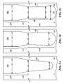
- FIGS. 1A through 1Hare cross-sectional drawings illustrating fabrication of trench capacitors according to the embodiments of the present invention.
- FIG. 2is a cross-sectional view of a memory cell using trench capacitors according to the embodiments of the present invention.
- FIGS. 3A , 3 B and 3 Care cross-sectional views illustrating alternative lower region trench geometries of trench capacitors according to the embodiments of the present invention.
- FIGS. 1A through 1Hare cross-sectional drawings illustrating fabrication of trench capacitors according to the embodiments of the present invention.
- a pad layer 115is formed and a trench 120 is etched in the substrate through an opening formed in the pad layer.
- Pad layer 115serves, among other uses, as a hardmask layer.
- Trench 120has three distinct regions, an upper region 125 adjacent to top surface 100 of substrate 105 , a middle region 130 and a lower region 135 .
- pad layer 115comprises a layer of silicon dioxide between about 2 nm and about 10 nm in thickness in contact with top surface 100 and a silicon nitride layer between about 100 nm and 2000 nm on the silicon dioxide layer.
- Additional one or more hardmask layerscan be formed on the pad layer 115 before the deep trench is etched.
- a layer (not shown) comprising boro-silicate glass (BSG)can be deposited on the pad layer 115 by chemical vapor deposition (CVD) and patterned along with the underlying pad layer 115 .
- the additional hardmask layersfacilitate the deep trench formation and can be removed after the deep trench 120 is etched.
- Upper region 125 of trench 120has a substantially uniform width W 1 along an axis 136 perpendicular to top surface 100 .
- Upper region 125 of trench 120extends a distance D 1 into substrate 105 .
- Sidewall region 137 of upper region 125 of trench 120is at an angle a 1 relative to top surface 100 of substrate 105 .
- Sidewall region 137 of upper region 125 of trench 120is substantially perpendicular to top surface 100 of substrate 105 .
- angle a 1is about 90°.
- angle a 1is between about 89.5° and about 90.5°.
- Sidewall region 137is essentially a trench region having a vertical sidewall (relative to top surface 100 ).
- Middle region 130 of trench 120has width W 1 where the middle region adjoins upper region 125 and a width W 2 where it adjoins lower region 135 .
- Middle region 130extends a distance D 2 into substrate 100 below upper region 125 .
- W 1is greater than W 2 .
- Sidewall region 138 of middle region 135is at an angle a 2 relative to top surface 100 of substrate 105 .
- Sidewall region 138 of middle region 130 of trench 120tapers inward toward axis 122 .
- angle a 2is about 1.0°.
- angle a 2is between about 3.0° and about 0.5°.
- the ratio (W 1 ⁇ W 2 )/W 1is less than about 0.2.
- W 1 -W 2is less than or equal to about 10 nm. In one example, W 1 is equal to less than about 90 nm and W 2 is equal to or less than about 80 nm. In one example, W 1 is equal to less than about 65 nm and W 2 is equal to or less than 55 nm.
- Sidewall region 138is essentially a trench region having a tapered sidewall (relative to top surface 100 ). In one example D 1 is between about four times and about five times D 2 .
- Lower region 135 of trench 120has width W 2 where the lower region adjoins middle region 130 and a width W 2 where it adjoins lower region 135 .
- Lower region 135 of trench 120has a substantially uniform width W 2 along axis 136 and extends a distance D 3 into substrate 105 below middle region 130 .
- Sidewall region 139 of lower region 135 of trench 120is essentially perpendicular to top surface 100 of substrate 100 in FIG. 1A .
- Sidewall region 139is essentially a sidewall region having a vertical sidewall (relative to top surface 100 ).
- FIGS. 3A , 3 B and 3 Cother geometries of lower region 135 are possible and are illustrated in FIGS. 3A , 3 B and 3 C and described infra.
- Trench 120may be formed by a reactive ion etch (RIE) process using a multiple step RIE process.
- Upper region 125 of trench 120may be formed by a first RIE process step
- middle region 130 of the trenchmay be formed by a second RIE process step different from the first RIE step process
- lower region 135 of the trenchmay be formed by one or more additional RIE process steps.
- Table Iillustrates exemplary first and second RIE process steps.
- a node dielectric layer 140is formed on a sidewall 145 (includes sidewall regions 137 , 138 and 139 illustrated in FIG. 1A and described supra) of trench 120 , on a bottom 150 of the trench and on a top surface 155 of pad layer 115 .
- node dielectricis formed by low pressure chemical vapor deposition (LPCVD) of silicon nitride between about 2.5 nm and about 6.0 nm thick followed by an optional thermal oxidation.
- node dielectriccomprises a high-k (dielectric constant) material between about 0.5 nm and about 6.0 nm thick formed by atomic layer deposition (ALD) or metalorganic chemical vapor deposition (MOCVD), examples of which include but are not limited metal oxides such as Ta 2 O 5 , BaTiO 3 , HfO 2 , ZrO 2 , Al 2 O 3 , or metal silicates such as HfSi x O y or HfSi x O y N z or combinations of layers thereof.
- a high-k dielectric materialhas a relative permittivity above about 10.
- trench 120is filled with a first electrically conductive fill material 160 .
- the first fill material 160preferably comprises N-type doped polysilicon.
- first fill material 160may comprise electrically conductive materials, including but not limited to, doped silicon germanium, tungsten, titanium, cobalt, copper, aluminum, other metals, tungsten silicide, titanium nitride, polysilicon and combinations thereof.
- first fill material 160is polysilicon, a void 165 may form in the polysilicon in upper region 125 of trench 120 .
- first polysilicon 160is removed from trench 120 so that a top surface 167 of first polysilicon 160 is within middle region 130 of trench 167 .
- Top surface 167is a distance D 4 from the top of middle region 130 .
- Node dielectric layer 140is also removed from all surfaces (particularly sidewall 145 of trench 120 ) no longer protected by first polysilicon 160 .
- first polysilicon 160is removed by a recess RIE process.
- CMPchemical-mechanical-polish
- node dielectric 140(if not removed during the recess RIE) is removed by wet etching with an etchant of hydrofluoric acid mixed with ethylene glycol.
- a dielectric collar 170is formed on sidewall 145 where sidewall 145 is not covered by node dielectric 140 and first polysilicon 160 .
- collar 170is formed by CVD deposition of a tetraethoxysilane (TEOS) oxide followed by an RIE process and is between about 15 nm and about 50 nm thick.
- TEOStetraethoxysilane
- RIEion etching
- a thermal oxidation processis performed to form a silicon dioxide (not shown) on the exposed sidewall 145 and on the top surface of the polysilicon 160 prior to the TEOS deposition.
- an annealing process at a temperature between 800° C. to 1200° C.is performed prior to the RIE process.
- collar 170comprises a low-k (dielectric constant) material, examples of which include but are not limited to hydrogen silsesquioxane polymer (HSQ), methyl silsesquioxane polymer (MSQ), SiLKTM (polyphenylene oligomer) manufactured by Dow Chemical, Midland, Tex., Black DiamondTM (methyl doped silica or SiO x (CH 3 ) y or SiC x O y H y or SiOCH) manufactured by Applied Materials, Santa Clara, Calif., organosilicate glass (SiCOH), and porous SiCOH between about 15 nm and about 40 nm thick.
- a low-k dielectric materialhas a relative permittivity of about 3.1 or less.
- trench 120is filled with a second electrically conductive fill material 175 and then second fill material is recessed back so a top surface 177 of second fill material 175 is within upper region 125 of trench 120 in a manner similar to that described supra for recessing first fill material 160 .
- second fill material 175preferably comprises N-type doped polysilicon.
- second fill material 175may comprise electrically conductive materials, including but not limited to, doped silicon germanium, tungsten, titanium, cobalt, copper, aluminum, other metals, tungsten silicide, titanium nitride, polysilicon and combinations thereof.
- collar 170is removed from sidewall 145 where the collar is not protected by second polysilicon 175 .
- Dry etch processingsuch as plasma etching
- wet etch processingsuch as etching in hydrofluoric acid containing etchants may be used depending on the composition of collar 170 .
- trench 120is filled with a third electrically conductive fill material 180 and then the third fill material recessed back so a top surface 182 of the second fill material is within upper region 125 of trench 120 but below top surface 100 of substrate 105 in a manner similar to that described supra for recessing first fill material 160 .
- third fill material 180preferably comprises N-type doped polysilicon.
- third fill material 180may comprise electrically conductive materials, including but not limited to, doped silicon germanium, tungsten, titanium, cobalt, copper, aluminum, other metals, tungsten silicide, titanium nitride, polysilicon and combinations thereof.
- Fabrication of a trench capacitor 185 according to the embodiments of the present inventionis essentially complete. Additional steps, described infra, may be performed to fabricate a dynamic access memory (DRAM) cell.
- DRAMdynamic access memory
- FIG. 2a cross-sectional view of a memory cell using trench capacitors according to the embodiments of the present invention.
- a trench isolation 190is formed in substrate 105 and partially into trench capacitor 185 .
- trench isolation 190may be formed by (1) etching trenches into substrate 105 and into a portion of trench capacitor 185 , using pad layer 115 (see FIG. 1H ) as a hardmask, (2) over-filling the trench with a dielectric material, such as TEOS oxide and (3) performing a CMP down to the pad layer.
- a dielectric materialsuch as TEOS oxide
- FET 200field effect transistor 200 is formed adjacent to and physically and electrically connected to trench capacitor 185 .
- FET 200includes a gate electrode 205 and dielectric spacers 210 formed over a gate dielectric 215 formed over a channel region 220 separating a first source/drain 225 from a second source/drain 230 .
- a buried strap 235(formed by out-diffusion of dopants from third polysilicon 180 provides an electrical connection between second source/drain 230 and third polysilicon 180 .
- FET 200is an n-channel FET (NFET).
- FIGS. 3A , 3 B and 3 Care cross-sectional views illustrating alternative lower region trench geometries of trench capacitors according to the embodiments of the present invention. Any of the trenches 120 A, 120 B or 120 C of respective FIGS. 3A , 3 B and 3 C may replace trench 120 of FIG. 1A as the starting trench for the fabrication of a trench capacitor according to the embodiments of the present invention.
- upper and middle regions 125 and 130 of trench 120 Aare the same as upper and middle regions 125 and 130 of trench 120 of FIG. 1A .
- a lower region 135 A of trench 120 Ahas an inward tapering sidewall region 139 A so a width W 3 at the bottom of the lower region is less than the width W 2 at the top of the lower region.
- upper and middle regions 125 and 130 of trench 120 Bare the same as upper and middle regions 125 and 130 of trench 120 of FIG. 1A .
- a lower region 135 B of trench 120 Bhas an outward tapering sidewall region 139 B so a width W 4 at the bottom of the lower region is greater than the width W 2 at the top of the lower region.
- upper and middle regions 125 and 130 of trench 120 Care the same as upper and middle regions 125 and 130 of trench 120 of FIG. 1A .
- a lower region 135 C of trench 120 Cincludes a vertical region 240 and a bulbous region 245 (the vertical region is between middle region 130 and bulbous region 245 ).
- Vertical region 240has a width W 2 and bulbous region 245 has a maximum width W 5 , where W 5 is greater than W 2 .
- Trenches 120 B and 120 Care known as a “bottle” trenches and when used for a trench capacitor results in a “bottle trench capacitor.”
- the present inventionprovides trench capacitor structures and a method of fabricating trench capacitors that is scalable to ever decreasing trench widths and that overcomes fabrication limits and capacitance and resistance problems of current trench capacitor designs.
Landscapes
- Engineering & Computer Science (AREA)
- Manufacturing & Machinery (AREA)
- Semiconductor Memories (AREA)
Abstract
Description
- This application is a division of U.S. patent application Ser. No. 11/427,065 filed on Jun. 28, 2006.
- The present invention relates to the field of semiconductor devices; more specifically, it relates to semiconductor trench capacitors and memory cells using the trench capacitors and method of fabricating the semiconductor trench capacitors and memory cells using the trench capacitors.
- A predominate use of trench capacitors is as the storage nodes of dynamic random access memory (DRAM) cells, though there are many other uses. As the density of DRAM increases and the photolithographic groundrules and resultant physical dimensions of the trench capacitors decrease, it has become increasingly difficult to fabricate the resultant narrow trenches. Additionally, narrow trenches have lower capacitance and higher resistance than wide trenches leading to lower reliability. Therefore, there is a need for trench capacitor structures and a method of fabricating trench capacitors that is scalable to ever decreasing trench widths and that overcomes fabrication limits and capacitance and resistance problems of current trench capacitor designs.
- A first aspect of the present invention is a structure, comprising: a substrate having a top surface defining a horizontal direction; a trench having contiguous upper, middle and lower regions, the middle region between the upper and lower regions, the trench extending from the top surface of the substrate into the substrate along an axis perpendicular to the top surface of the substrate, the axis defining a vertical direction; the upper region of the trench adjacent to the top surface of the substrate having a vertical sidewall profile and a first width in the horizontal direction; and the middle region of the trench having a tapered sidewall profile, a width in the horizontal direction of the middle region at a juncture of the upper region and the middle region being the first width and being greater than a second width in the horizontal direction of the middle region at a juncture of the middle region and the lower region.
- A second aspect of the present invention is a method forming a trench in a substrate having a top surface defining a horizontal direction, comprising: forming a masking layer on the top surface of the substrate; forming an opening in the masking layer to define a perimeter of a trench; and forming the trench in the substrate through the opening, the trench having contiguous upper, middle and lower regions, the middle region between the upper and lower regions, the trench extending from the top surface of the substrate into the substrate along an axis perpendicular to the top surface of the substrate, the axis defining a vertical direction, the upper region of the trench adjacent to the top surface of the substrate having a vertical sidewall profile and a first width in the horizontal direction, the middle region of the trench having a tapered sidewall profile, a width in the horizontal direction of the middle region at a juncture of the upper region and the middle region being the first width and being greater than a second width in the horizontal direction of the middle region at a juncture of the middle region and the lower region.
- A third aspect of the present invention is a memory cell, comprising: a trench capacitor in a substrate, the trench capacitor having contiguous upper, middle and lower regions, the middle region between the upper and lower regions, the trench extending from a top surface of the substrate into the substrate along an axis perpendicular to the top surface of the substrate, the axis defining a vertical direction; the upper region of the trench adjacent to the top surface of the substrate having a vertical sidewall profile; the middle region of the trench having a tapered sidewall profile, a width in the horizontal direction of the middle region at a juncture of the upper region and the middle region being greater than a width in the horizontal direction of the middle region at a juncture of the middle region and the lower region; and a field effect transistor comprising a gate electrode separated from a channel region in the substrate by a gate dielectric layer on the top surface of the substrate and first and second source/drains formed in the substrate on opposite side of the channel region, the second source/drain electrically connected to an electrode formed in the trench.
- A fourth aspect of the present invention is a method of fabricating a memory cell, comprising: forming a trench capacitor in a substrate, the trench capacitor having contiguous upper, middle and lower regions, the middle region between the upper and lower regions, the trench extending from a top surface of the substrate into the substrate along an axis perpendicular to the top surface of the substrate, the axis defining a vertical direction; the upper region of the trench adjacent to the top surface of the substrate having a vertical sidewall profile; the middle region of the trench having a tapered sidewall profile, a width in the horizontal direction of the middle region at a juncture of the upper region and the middle region being greater than a width in the horizontal direction of the middle region at a juncture of the middle region and the lower region; and forming a field effect transistor comprising a gate electrode separated from a channel region in the substrate by a gate dielectric layer on the top surface of the substrate and first and second source/drains formed in the substrate on opposite side of the channel region, the second source/drain electrically connected to an electrode formed in the trench.
- The features of the invention are set forth in the appended claims. The invention itself, however, will be best understood by reference to the following detailed description of an illustrative embodiment when read in conjunction with the accompanying drawings, wherein:
FIGS. 1A through 1H are cross-sectional drawings illustrating fabrication of trench capacitors according to the embodiments of the present invention;FIG. 2 is a cross-sectional view of a memory cell using trench capacitors according to the embodiments of the present invention; andFIGS. 3A ,3B and3C are cross-sectional views illustrating alternative lower region trench geometries of trench capacitors according to the embodiments of the present invention.FIGS. 1A through 1H are cross-sectional drawings illustrating fabrication of trench capacitors according to the embodiments of the present invention. InFIG. 1A , on atop surface 100 of a silicon substrate105 apad layer 115 is formed and atrench 120 is etched in the substrate through an opening formed in the pad layer.Pad layer 115, serves, among other uses, as a hardmask layer.Trench 120 has three distinct regions, anupper region 125 adjacent totop surface 100 ofsubstrate 105, amiddle region 130 and alower region 135. In one example,pad layer 115 comprises a layer of silicon dioxide between about 2 nm and about 10 nm in thickness in contact withtop surface 100 and a silicon nitride layer between about 100 nm and 2000 nm on the silicon dioxide layer. Additional one or more hardmask layers (not shown) can be formed on thepad layer 115 before the deep trench is etched. For example, a layer (not shown) comprising boro-silicate glass (BSG) can be deposited on thepad layer 115 by chemical vapor deposition (CVD) and patterned along with theunderlying pad layer 115. The additional hardmask layers facilitate the deep trench formation and can be removed after thedeep trench 120 is etched.Upper region 125 oftrench 120 has a substantially uniform width W1 along anaxis 136 perpendicular totop surface 100.Upper region 125 oftrench 120 extends a distance D1 intosubstrate 105.Sidewall region 137 ofupper region 125 oftrench 120 is at an angle a1 relative totop surface 100 ofsubstrate 105.Sidewall region 137 ofupper region 125 oftrench 120 is substantially perpendicular totop surface 100 ofsubstrate 105. In one example, angle a1 is about 90°. In one example, angle a1 is between about 89.5° and about 90.5°.Sidewall region 137 is essentially a trench region having a vertical sidewall (relative to top surface100).Middle region 130 oftrench 120 has width W1 where the middle region adjoinsupper region 125 and a width W2 where it adjoinslower region 135.Middle region 130 extends a distance D2 intosubstrate 100 belowupper region 125. W1 is greater than W2.Sidewall region 138 ofmiddle region 135 is at an angle a2 relative totop surface 100 ofsubstrate 105. Sidewallregion 138 ofmiddle region 130 oftrench 120 tapers inward towardaxis 122. In one example, angle a2 is about 1.0°. In one example, angle a2 is between about 3.0° and about 0.5°. In one example, the ratio (W1−W2)/W1 is less than about 0.2. In one example, W1-W2 is less than or equal to about 10 nm. In one example, W1 is equal to less than about 90 nm and W2 is equal to or less than about 80 nm. In one example, W1 is equal to less than about 65 nm and W2 is equal to or less than 55 nm.Sidewall region 138 is essentially a trench region having a tapered sidewall (relative to top surface100). In one example D1 is between about four times and about five times D2.Lower region 135 oftrench 120 has width W2 where the lower region adjoinsmiddle region 130 and a width W2 where it adjoinslower region 135.Lower region 135 oftrench 120 has a substantially uniform width W2 alongaxis 136 and extends a distance D3 intosubstrate 105 belowmiddle region 130.Sidewall region 139 oflower region 135 oftrench 120 is essentially perpendicular totop surface 100 ofsubstrate 100 inFIG. 1A .Sidewall region 139 is essentially a sidewall region having a vertical sidewall (relative to top surface100). However, other geometries oflower region 135 are possible and are illustrated inFIGS. 3A ,3B and3C and described infra.Trench 120 may be formed by a reactive ion etch (RIE) process using a multiple step RIE process.Upper region 125 oftrench 120 may be formed by a first RIE process step,middle region 130 of the trench may be formed by a second RIE process step different from the first RIE step process andlower region 135 of the trench may be formed by one or more additional RIE process steps. Table I illustrates exemplary first and second RIE process steps.TABLE I Exemplary RIE Process Steps for a Trench with W1 less than or equal to 90 nm (300 mm Wafer, about 20% Trench Area) Trench Region Upper Middle Lower RIE Step 1 Step 2 Step 3 Bias power (W) 1300 1500 1800 Pressure (mT) 150 150 200 O2(sccm) 28 23 16 NF3(sccm) 36 36 32 HBr (sccm) 300 300 300 Profile of Region Vertical Tapered Vertical Depth of Region (um) 1.2 (D1) 0.3 (D2) 6.0 (D3) - A person of ordinary skill in the art, will be able to modify the conditions given in Table I to fit other trench profiles and geometries without undue experimentation.
- In
FIG. 1B , anode dielectric layer 140 is formed on a sidewall145 (includessidewall regions FIG. 1A and described supra) oftrench 120, on abottom 150 of the trench and on atop surface 155 ofpad layer 115. In one example node dielectric is formed by low pressure chemical vapor deposition (LPCVD) of silicon nitride between about 2.5 nm and about 6.0 nm thick followed by an optional thermal oxidation. In one example, node dielectric comprises a high-k (dielectric constant) material between about 0.5 nm and about 6.0 nm thick formed by atomic layer deposition (ALD) or metalorganic chemical vapor deposition (MOCVD), examples of which include but are not limited metal oxides such as Ta2O5, BaTiO3, HfO2, ZrO2, Al2O3, or metal silicates such as HfSixOyor HfSixOyNzor combinations of layers thereof. A high-k dielectric material has a relative permittivity above about 10. - In
FIG. 1C ,trench 120 is filled with a first electricallyconductive fill material 160. In one example, thefirst fill material 160 preferably comprises N-type doped polysilicon. Alternatively,first fill material 160 may comprise electrically conductive materials, including but not limited to, doped silicon germanium, tungsten, titanium, cobalt, copper, aluminum, other metals, tungsten silicide, titanium nitride, polysilicon and combinations thereof. In some cases, whenfirst fill material 160 is polysilicon, a void165 may form in the polysilicon inupper region 125 oftrench 120. - Because the upper part of the trench is vertical for a significant distance before is tapers down, filling of the trench with polysilicon is more easily accomplished and any voids formed do not extend far enough into the tapered portion of the trench and can be removed or their disruption of fill interfaces drastically reduced during subsequent processing steps.
- In
FIG. 1D , a portion offirst polysilicon 160 is removed fromtrench 120 so that atop surface 167 offirst polysilicon 160 is withinmiddle region 130 oftrench 167.Top surface 167 is a distance D4 from the top ofmiddle region 130.Node dielectric layer 140 is also removed from all surfaces (particularlysidewall 145 of trench120) no longer protected byfirst polysilicon 160. In one example,first polysilicon 160 is removed by a recess RIE process. In one example, a chemical-mechanical-polish (CMP) is performed to coplanarize a top surface offirst polysilicon 160 intrench 120 with atopsurface 155 ofpad layer 115 prior to a recess RIE process. In one example, node dielectric140 (if not removed during the recess RIE) is removed by wet etching with an etchant of hydrofluoric acid mixed with ethylene glycol. - In
FIG. 1E , adielectric collar 170 is formed onsidewall 145 wheresidewall 145 is not covered bynode dielectric 140 andfirst polysilicon 160. In one example,collar 170 is formed by CVD deposition of a tetraethoxysilane (TEOS) oxide followed by an RIE process and is between about 15 nm and about 50 nm thick. In one example, a thermal oxidation process is performed to form a silicon dioxide (not shown) on the exposedsidewall 145 and on the top surface of thepolysilicon 160 prior to the TEOS deposition. In one example, an annealing process at a temperature between 800° C. to 1200° C. is performed prior to the RIE process. In one example,collar 170 comprises a low-k (dielectric constant) material, examples of which include but are not limited to hydrogen silsesquioxane polymer (HSQ), methyl silsesquioxane polymer (MSQ), SiLK™ (polyphenylene oligomer) manufactured by Dow Chemical, Midland, Tex., Black Diamond™ (methyl doped silica or SiOx(CH3)yor SiCxOyHyor SiOCH) manufactured by Applied Materials, Santa Clara, Calif., organosilicate glass (SiCOH), and porous SiCOH between about 15 nm and about 40 nm thick. A low-k dielectric material has a relative permittivity of about 3.1 or less. - Because the upper part of the trench is vertical for a significant distance before is tapers down, formation of collars is easily accomplished and the collars may be kept relatively thick with no fear of reducing the cross-sectional area of the polysilicon fill which would increase the resistance of the capacitor.
- In
FIG. 1F ,trench 120 is filled with a second electricallyconductive fill material 175 and then second fill material is recessed back so atop surface 177 ofsecond fill material 175 is withinupper region 125 oftrench 120 in a manner similar to that described supra for recessingfirst fill material 160. In one example,second fill material 175 preferably comprises N-type doped polysilicon. Alternatively,second fill material 175 may comprise electrically conductive materials, including but not limited to, doped silicon germanium, tungsten, titanium, cobalt, copper, aluminum, other metals, tungsten silicide, titanium nitride, polysilicon and combinations thereof. - In
FIG. 1G ,collar 170 is removed fromsidewall 145 where the collar is not protected bysecond polysilicon 175. Dry etch processing (such as plasma etching) or wet etch processing (such as etching in hydrofluoric acid containing etchants) may be used depending on the composition ofcollar 170. - In
FIG. 1H ,trench 120 is filled with a third electricallyconductive fill material 180 and then the third fill material recessed back so atop surface 182 of the second fill material is withinupper region 125 oftrench 120 but belowtop surface 100 ofsubstrate 105 in a manner similar to that described supra for recessingfirst fill material 160. In one example,third fill material 180 preferably comprises N-type doped polysilicon. Alternatively,third fill material 180 may comprise electrically conductive materials, including but not limited to, doped silicon germanium, tungsten, titanium, cobalt, copper, aluminum, other metals, tungsten silicide, titanium nitride, polysilicon and combinations thereof. - Fabrication of a
trench capacitor 185 according to the embodiments of the present invention is essentially complete. Additional steps, described infra, may be performed to fabricate a dynamic access memory (DRAM) cell. FIG. 2 a cross-sectional view of a memory cell using trench capacitors according to the embodiments of the present invention. InFIG. 2 , atrench isolation 190 is formed insubstrate 105 and partially intotrench capacitor 185. In one example,trench isolation 190 may be formed by (1) etching trenches intosubstrate 105 and into a portion oftrench capacitor 185, using pad layer115 (seeFIG. 1H ) as a hardmask, (2) over-filling the trench with a dielectric material, such as TEOS oxide and (3) performing a CMP down to the pad layer.- Next, pad layer115 (see
FIG. 1H ) is removed and a field effect transistor (FET)200 is formed adjacent to and physically and electrically connected totrench capacitor 185. Formation of FETs is well known in the art.FET 200 includes agate electrode 205 anddielectric spacers 210 formed over agate dielectric 215 formed over achannel region 220 separating a first source/drain 225 from a second source/drain 230. A buried strap235 (formed by out-diffusion of dopants fromthird polysilicon 180 provides an electrical connection between second source/drain 230 andthird polysilicon 180. In one example.FET 200 is an n-channel FET (NFET). FIGS. 3A ,3B and3C are cross-sectional views illustrating alternative lower region trench geometries of trench capacitors according to the embodiments of the present invention. Any of thetrenches FIGS. 3A ,3B and3C may replacetrench 120 ofFIG. 1A as the starting trench for the fabrication of a trench capacitor according to the embodiments of the present invention.- In
FIG. 3A , upper andmiddle regions trench 120A are the same as upper andmiddle regions trench 120 ofFIG. 1A . Alower region 135A oftrench 120A has an inwardtapering sidewall region 139A so a width W3 at the bottom of the lower region is less than the width W2 at the top of the lower region. - In
FIG. 3B , upper andmiddle regions trench 120B are the same as upper andmiddle regions trench 120 ofFIG. 1A . Alower region 135B oftrench 120B has an outwardtapering sidewall region 139B so a width W4 at the bottom of the lower region is greater than the width W2 at the top of the lower region. - In
FIG. 3C , upper andmiddle regions trench 120C are the same as upper andmiddle regions trench 120 ofFIG. 1A . Alower region 135C oftrench 120C includes avertical region 240 and a bulbous region245 (the vertical region is betweenmiddle region 130 and bulbous region245).Vertical region 240 has a width W2 andbulbous region 245 has a maximum width W5, where W5 is greater than W2.Trenches - Thus the present invention provides trench capacitor structures and a method of fabricating trench capacitors that is scalable to ever decreasing trench widths and that overcomes fabrication limits and capacitance and resistance problems of current trench capacitor designs.
- The description of the embodiments of the present invention is given above for the understanding of the present invention. It will be understood that the invention is not limited to the particular embodiments described herein, but is capable of various modifications, rearrangements and substitutions as will now become apparent to those skilled in the art without departing from the scope of the invention. Therefore, it is intended that the following claims cover all such modifications and changes as fall within the true spirit and scope of the invention.
Claims (20)
Priority Applications (1)
| Application Number | Priority Date | Filing Date | Title |
|---|---|---|---|
| US12/138,536US7888722B2 (en) | 2006-06-28 | 2008-06-13 | Trench capacitors and memory cells using trench capacitors |
Applications Claiming Priority (2)
| Application Number | Priority Date | Filing Date | Title |
|---|---|---|---|
| US11/427,065US7709320B2 (en) | 2006-06-28 | 2006-06-28 | Method of fabricating trench capacitors and memory cells using trench capacitors |
| US12/138,536US7888722B2 (en) | 2006-06-28 | 2008-06-13 | Trench capacitors and memory cells using trench capacitors |
Related Parent Applications (1)
| Application Number | Title | Priority Date | Filing Date |
|---|---|---|---|
| US11/427,065DivisionUS7709320B2 (en) | 2006-06-28 | 2006-06-28 | Method of fabricating trench capacitors and memory cells using trench capacitors |
Publications (2)
| Publication Number | Publication Date |
|---|---|
| US20080246068A1true US20080246068A1 (en) | 2008-10-09 |
| US7888722B2 US7888722B2 (en) | 2011-02-15 |
Family
ID=38875695
Family Applications (2)
| Application Number | Title | Priority Date | Filing Date |
|---|---|---|---|
| US11/427,065Expired - Fee RelatedUS7709320B2 (en) | 2006-06-28 | 2006-06-28 | Method of fabricating trench capacitors and memory cells using trench capacitors |
| US12/138,536Expired - Fee RelatedUS7888722B2 (en) | 2006-06-28 | 2008-06-13 | Trench capacitors and memory cells using trench capacitors |
Family Applications Before (1)
| Application Number | Title | Priority Date | Filing Date |
|---|---|---|---|
| US11/427,065Expired - Fee RelatedUS7709320B2 (en) | 2006-06-28 | 2006-06-28 | Method of fabricating trench capacitors and memory cells using trench capacitors |
Country Status (1)
| Country | Link |
|---|---|
| US (2) | US7709320B2 (en) |
Cited By (4)
| Publication number | Priority date | Publication date | Assignee | Title |
|---|---|---|---|---|
| US20100129982A1 (en)* | 2008-11-24 | 2010-05-27 | Applied Materials, Inc. | Integration sequences with top surface profile modification |
| US20100130007A1 (en)* | 2008-11-24 | 2010-05-27 | Applied Materials, Inc. | Bottom up plating by organic surface passivation and differential plating retardation |
| US20140054683A1 (en)* | 2009-11-17 | 2014-02-27 | Chiao-Shun Chuang | Trench devices having improved breakdown voltages and method for manufacturing same |
| US20150214134A1 (en)* | 2014-01-30 | 2015-07-30 | Kabushiki Kaisha Toshiba | Semiconductor device and semiconductor device manufacturing method |
Families Citing this family (24)
| Publication number | Priority date | Publication date | Assignee | Title |
|---|---|---|---|---|
| KR101052868B1 (en)* | 2008-02-29 | 2011-07-29 | 주식회사 하이닉스반도체 | SOI element and its manufacturing method |
| US8492817B2 (en) | 2009-02-13 | 2013-07-23 | International Business Machines Corporation | Highly scalable trench capacitor |
| JP2010272758A (en)* | 2009-05-22 | 2010-12-02 | Hitachi High-Technologies Corp | Plasma etching method for material to be etched |
| US8507915B2 (en)* | 2011-11-30 | 2013-08-13 | International Business Machines Corporation | Low resistance embedded strap for a trench capacitor |
| US8541302B2 (en)* | 2011-12-15 | 2013-09-24 | Semiconductor Components Industries, Llc | Electronic device including a trench with a facet and a conductive structure therein and a process of forming the same |
| US8592279B2 (en) | 2011-12-15 | 2013-11-26 | Semicondcutor Components Industries, LLC | Electronic device including a tapered trench and a conductive structure therein and a process of forming the same |
| US8637365B2 (en)* | 2012-06-06 | 2014-01-28 | International Business Machines Corporation | Spacer isolation in deep trench |
| KR20140023735A (en)* | 2012-08-17 | 2014-02-27 | 삼성전자주식회사 | A semiconductor device including transistors |
| JP6514206B2 (en)* | 2013-12-17 | 2019-05-15 | アグファ・ナームローゼ・フェンノートシャップAgfa Nv | Radiographic flat panel detector with light weight x-ray shield and method of making same |
| US9543208B2 (en)* | 2014-02-24 | 2017-01-10 | Infineon Technologies Ag | Method of singulating semiconductor devices using isolation trenches |
| US9960168B2 (en)* | 2014-12-24 | 2018-05-01 | Globalfoundries Inc. | Capacitor strap connection structure and fabrication method |
| US10049927B2 (en)* | 2016-06-10 | 2018-08-14 | Applied Materials, Inc. | Seam-healing method upon supra-atmospheric process in diffusion promoting ambient |
| US10224224B2 (en) | 2017-03-10 | 2019-03-05 | Micromaterials, LLC | High pressure wafer processing systems and related methods |
| US10622214B2 (en) | 2017-05-25 | 2020-04-14 | Applied Materials, Inc. | Tungsten defluorination by high pressure treatment |
| US10276411B2 (en) | 2017-08-18 | 2019-04-30 | Applied Materials, Inc. | High pressure and high temperature anneal chamber |
| WO2019036157A1 (en) | 2017-08-18 | 2019-02-21 | Applied Materials, Inc. | High pressure and high temperature anneal chamber |
| CN117936420A (en) | 2017-11-11 | 2024-04-26 | 微材料有限责任公司 | Gas delivery system for high pressure processing chamber |
| KR20200075892A (en) | 2017-11-17 | 2020-06-26 | 어플라이드 머티어리얼스, 인코포레이티드 | Condenser system for high pressure treatment systems |
| SG11202008256WA (en) | 2018-03-09 | 2020-09-29 | Applied Materials Inc | High pressure annealing process for metal containing materials |
| US10950429B2 (en) | 2018-05-08 | 2021-03-16 | Applied Materials, Inc. | Methods of forming amorphous carbon hard mask layers and hard mask layers formed therefrom |
| US10748783B2 (en) | 2018-07-25 | 2020-08-18 | Applied Materials, Inc. | Gas delivery module |
| WO2020117462A1 (en) | 2018-12-07 | 2020-06-11 | Applied Materials, Inc. | Semiconductor processing system |
| US11901222B2 (en) | 2020-02-17 | 2024-02-13 | Applied Materials, Inc. | Multi-step process for flowable gap-fill film |
| US11610899B2 (en)* | 2021-06-15 | 2023-03-21 | Nanya Technology Corporation | Memory cell, memory array and method for defining active area of memory cell |
Citations (57)
| Publication number | Priority date | Publication date | Assignee | Title |
|---|---|---|---|---|
| US5604159A (en)* | 1994-01-31 | 1997-02-18 | Motorola, Inc. | Method of making a contact structure |
| US5641694A (en)* | 1994-12-22 | 1997-06-24 | International Business Machines Corporation | Method of fabricating vertical epitaxial SOI transistor |
| US5891807A (en)* | 1997-09-25 | 1999-04-06 | Siemens Aktiengesellschaft | Formation of a bottle shaped trench |
| US5905279A (en)* | 1996-04-09 | 1999-05-18 | Kabushiki Kaisha Toshiba | Low resistant trench fill for a semiconductor device |
| US5914523A (en)* | 1998-02-17 | 1999-06-22 | National Semiconductor Corp. | Semiconductor device trench isolation structure with polysilicon bias voltage contact |
| US5930107A (en)* | 1995-10-19 | 1999-07-27 | International Business Machines Corporation | Dual trench capacitor |
| US6018174A (en)* | 1998-04-06 | 2000-01-25 | Siemens Aktiengesellschaft | Bottle-shaped trench capacitor with epi buried layer |
| US6103585A (en)* | 1998-06-09 | 2000-08-15 | Siemens Aktiengesellschaft | Method of forming deep trench capacitors |
| US6127278A (en)* | 1997-06-02 | 2000-10-03 | Applied Materials, Inc. | Etch process for forming high aspect ratio trenched in silicon |
| US6207494B1 (en)* | 1994-12-29 | 2001-03-27 | Infineon Technologies Corporation | Isolation collar nitride liner for DRAM process improvement |
| US6232171B1 (en)* | 1999-01-11 | 2001-05-15 | Promos Technology, Inc. | Technique of bottle-shaped deep trench formation |
| US6274457B1 (en)* | 1997-08-28 | 2001-08-14 | Mitsubishi Denki Kabushiki Kaisha | Method for manufacturing an isolation trench having plural profile angles |
| US6281068B1 (en)* | 1998-04-30 | 2001-08-28 | International Business Machines Corporation | Method for buried plate formation in deep trench capacitors |
| US20010023134A1 (en)* | 1998-03-31 | 2001-09-20 | Hiroyuki Akatsu | Method of manufacturing a semiconductor device including a seamless shallow trench isolation step |
| US6319788B1 (en)* | 1999-12-14 | 2001-11-20 | Infineon Technologies North America Corp. | Semiconductor structure and manufacturing methods |
| US20010044180A1 (en)* | 2000-04-12 | 2001-11-22 | Martin Schrems | Trench capacitor and method for fabricating a trench capacitor |
| US6342450B1 (en)* | 1999-01-07 | 2002-01-29 | International Business Machines Corporation | Method of forming insulating spacers in DRAM chips |
| US20020036310A1 (en)* | 2000-09-23 | 2002-03-28 | Jorn Lutzen | Trench capacitor having an insulation collar, and method of producing such a trench capacitor |
| US6365485B1 (en)* | 2000-04-19 | 2002-04-02 | Promos Tech., Inc, | DRAM technology of buried plate formation of bottle-shaped deep trench |
| US6380095B1 (en)* | 1998-06-22 | 2002-04-30 | Applied Materials, Inc. | Silicon trench etch using silicon-containing precursors to reduce or avoid mask erosion |
| US6440792B1 (en)* | 1999-11-05 | 2002-08-27 | Promos Technology, Inc. | DRAM technology of storage node formation and no conduction/isolation process of bottle-shaped deep trench |
| US20020132422A1 (en)* | 2001-03-13 | 2002-09-19 | Infineon Technologies North America Corp. | Method of deep trench formation with improved profile control and surface area |
| US20030020112A1 (en)* | 2001-07-24 | 2003-01-30 | Helmut Tews | Method of preparing buried LOCOS collar in trench DRAMS |
| US20030045052A1 (en)* | 2001-08-31 | 2003-03-06 | Albert Birner | Method for fabricating a trench structure |
| US20030073271A1 (en)* | 2001-10-12 | 2003-04-17 | Albert Birner | Method of forming a vertical field-effect transistor device |
| US20030143809A1 (en)* | 2002-01-25 | 2003-07-31 | Infineon Technologies North America Corp. | Method for achieving high self-aligning vertical gate studs relative to the support isolation level |
| US20030155609A1 (en)* | 2002-02-20 | 2003-08-21 | International Business Machines Corporation | Self-aligned punch through stop for 6F2 rotated hybrid dram cell |
| US20030173618A1 (en)* | 2002-02-21 | 2003-09-18 | Markus Zundel | MOS transistor device |
| US6674113B2 (en)* | 2001-09-25 | 2004-01-06 | Infineon Technologies Ag | Trench capacitor and method for manufacturing the same |
| US6713341B2 (en)* | 2002-02-05 | 2004-03-30 | Nanya Technology Corporation | Method of forming a bottle-shaped trench in a semiconductor substrate |
| US6716696B2 (en)* | 2002-01-28 | 2004-04-06 | Nanya Technology Corporation | Method of forming a bottle-shaped trench in a semiconductor substrate |
| US6762447B1 (en)* | 1999-02-05 | 2004-07-13 | Infineon Technologies North America Corp. | Field-shield-trench isolation for gigabit DRAMs |
| US20040180510A1 (en)* | 2003-03-12 | 2004-09-16 | Infineon Technologies North America Corp. | Method to fill deep trench structures with void-free polysilicon or silicon |
| US20040259368A1 (en)* | 2003-06-23 | 2004-12-23 | Su-Chen Lai | Method for forming a bottle-shaped trench |
| US20050093080A1 (en)* | 2003-09-09 | 2005-05-05 | Yoshinori Kitamura | Semiconductor device and method of manufacturing the same |
| US20050212027A1 (en)* | 2004-03-29 | 2005-09-29 | International Business Machines Corporation | Vertical device with optimal trench shape |
| US20050285175A1 (en)* | 2004-06-23 | 2005-12-29 | International Business Machines Corporation | Vertical SOI Device |
| US6989561B2 (en)* | 2003-12-02 | 2006-01-24 | Nanya Technology Corp. | Trench capacitor structure |
| US20060049455A1 (en)* | 2004-09-09 | 2006-03-09 | Se-Myeong Jang | Semiconductor devices with local recess channel transistors and methods of manufacturing the same |
| US7038289B2 (en)* | 2001-06-14 | 2006-05-02 | Stmicroelectronics Sa | Deep insulating trench |
| US20060145247A1 (en)* | 2004-11-30 | 2006-07-06 | Markus Zundel | Trench transistor and method for producing it |
| US7109543B2 (en)* | 2001-12-24 | 2006-09-19 | Dongbuanam Semiconductor Inc. | Semiconductor device having trench capacitor and method for fabricating the same |
| US20060231877A1 (en)* | 2005-04-14 | 2006-10-19 | Keiichi Takenaka | Semiconductor device |
| US7132324B2 (en)* | 2004-12-09 | 2006-11-07 | International Business Machines Corporation | SOI device with different crystallographic orientations |
| US20060255390A1 (en)* | 2005-05-16 | 2006-11-16 | Kabushiki Kaisha Toshiba | Semiconductor device and method of manufacturing the same |
| US7153738B2 (en)* | 2005-05-19 | 2006-12-26 | International Business Machines Corporation | Method for making a trench memory cell |
| US20070059897A1 (en)* | 2005-09-09 | 2007-03-15 | Armin Tilke | Isolation for semiconductor devices |
| US20070145416A1 (en)* | 2005-12-28 | 2007-06-28 | Kabushiki Kaisha Toshiba | Semiconductor device |
| US20070148893A1 (en)* | 2005-12-22 | 2007-06-28 | Andrei Josiek | Method of forming a doped semiconductor portion |
| US20070164397A1 (en)* | 2004-06-15 | 2007-07-19 | Kangguo Cheng | Process for forming a buried plate |
| US20070189057A1 (en)* | 2006-01-10 | 2007-08-16 | International Business Machines Corporation | Multiple port memory having a plurality of parallel connected trench capacitors in a cell |
| US20070205489A1 (en)* | 2006-03-01 | 2007-09-06 | Armin Tilke | Methods of fabricating isolation regions of semiconductor devices and structures thereof |
| US20070224757A1 (en)* | 2004-03-30 | 2007-09-27 | International Business Machines Corporation | Offset vertical device |
| US20070296012A1 (en)* | 2004-11-15 | 2007-12-27 | International Business Machines Corporation | Structure and method for accurate deep trench resistance measurement |
| US20080035978A1 (en)* | 2006-02-10 | 2008-02-14 | International Business Machines Corporation | Method to eliminate arsenic contamination in trench capacitors |
| US20080290448A1 (en)* | 2007-05-22 | 2008-11-27 | Armin Tilke | Semiconductor devices and methods of manufacture thereof |
| US7553767B2 (en)* | 2005-09-29 | 2009-06-30 | Hynix Semiconductor Inc. | Method for fabricating semiconductor device having taper type trench |
Family Cites Families (7)
| Publication number | Priority date | Publication date | Assignee | Title |
|---|---|---|---|---|
| US7439568B2 (en)* | 2005-02-10 | 2008-10-21 | International Business Machines Corporation | Vertical body-contacted SOI transistor |
| US7382019B2 (en)* | 2005-04-26 | 2008-06-03 | Fairchild Semiconductor Corporation | Trench gate FETs with reduced gate to drain charge |
| US7375413B2 (en)* | 2006-05-26 | 2008-05-20 | International Business Machines Corporation | Trench widening without merging |
| US7560360B2 (en)* | 2006-08-30 | 2009-07-14 | International Business Machines Corporation | Methods for enhancing trench capacitance and trench capacitor |
| US7575970B2 (en)* | 2006-09-07 | 2009-08-18 | International Business Machines Corporation | Deep trench capacitor through SOI substrate and methods of forming |
| US7494891B2 (en)* | 2006-09-21 | 2009-02-24 | International Business Machines Corporation | Trench capacitor with void-free conductor fill |
| US7808028B2 (en)* | 2007-04-18 | 2010-10-05 | International Business Machines Corporation | Trench structure and method of forming trench structure |
- 2006
- 2006-06-28USUS11/427,065patent/US7709320B2/ennot_activeExpired - Fee Related
- 2008
- 2008-06-13USUS12/138,536patent/US7888722B2/ennot_activeExpired - Fee Related
Patent Citations (65)
| Publication number | Priority date | Publication date | Assignee | Title |
|---|---|---|---|---|
| US5604159A (en)* | 1994-01-31 | 1997-02-18 | Motorola, Inc. | Method of making a contact structure |
| US5641694A (en)* | 1994-12-22 | 1997-06-24 | International Business Machines Corporation | Method of fabricating vertical epitaxial SOI transistor |
| US5744386A (en)* | 1994-12-22 | 1998-04-28 | International Business Machines Corporation | Method of fabricating a memory cell in a substrate trench |
| US6207494B1 (en)* | 1994-12-29 | 2001-03-27 | Infineon Technologies Corporation | Isolation collar nitride liner for DRAM process improvement |
| US5930107A (en)* | 1995-10-19 | 1999-07-27 | International Business Machines Corporation | Dual trench capacitor |
| US5905279A (en)* | 1996-04-09 | 1999-05-18 | Kabushiki Kaisha Toshiba | Low resistant trench fill for a semiconductor device |
| US6127278A (en)* | 1997-06-02 | 2000-10-03 | Applied Materials, Inc. | Etch process for forming high aspect ratio trenched in silicon |
| US6274457B1 (en)* | 1997-08-28 | 2001-08-14 | Mitsubishi Denki Kabushiki Kaisha | Method for manufacturing an isolation trench having plural profile angles |
| US5891807A (en)* | 1997-09-25 | 1999-04-06 | Siemens Aktiengesellschaft | Formation of a bottle shaped trench |
| US5914523A (en)* | 1998-02-17 | 1999-06-22 | National Semiconductor Corp. | Semiconductor device trench isolation structure with polysilicon bias voltage contact |
| US20010023134A1 (en)* | 1998-03-31 | 2001-09-20 | Hiroyuki Akatsu | Method of manufacturing a semiconductor device including a seamless shallow trench isolation step |
| US6018174A (en)* | 1998-04-06 | 2000-01-25 | Siemens Aktiengesellschaft | Bottle-shaped trench capacitor with epi buried layer |
| US6281068B1 (en)* | 1998-04-30 | 2001-08-28 | International Business Machines Corporation | Method for buried plate formation in deep trench capacitors |
| US6103585A (en)* | 1998-06-09 | 2000-08-15 | Siemens Aktiengesellschaft | Method of forming deep trench capacitors |
| US6380095B1 (en)* | 1998-06-22 | 2002-04-30 | Applied Materials, Inc. | Silicon trench etch using silicon-containing precursors to reduce or avoid mask erosion |
| US6342450B1 (en)* | 1999-01-07 | 2002-01-29 | International Business Machines Corporation | Method of forming insulating spacers in DRAM chips |
| US6232171B1 (en)* | 1999-01-11 | 2001-05-15 | Promos Technology, Inc. | Technique of bottle-shaped deep trench formation |
| US6762447B1 (en)* | 1999-02-05 | 2004-07-13 | Infineon Technologies North America Corp. | Field-shield-trench isolation for gigabit DRAMs |
| US6440792B1 (en)* | 1999-11-05 | 2002-08-27 | Promos Technology, Inc. | DRAM technology of storage node formation and no conduction/isolation process of bottle-shaped deep trench |
| US6319788B1 (en)* | 1999-12-14 | 2001-11-20 | Infineon Technologies North America Corp. | Semiconductor structure and manufacturing methods |
| US20010044180A1 (en)* | 2000-04-12 | 2001-11-22 | Martin Schrems | Trench capacitor and method for fabricating a trench capacitor |
| US6365485B1 (en)* | 2000-04-19 | 2002-04-02 | Promos Tech., Inc, | DRAM technology of buried plate formation of bottle-shaped deep trench |
| US20020036310A1 (en)* | 2000-09-23 | 2002-03-28 | Jorn Lutzen | Trench capacitor having an insulation collar, and method of producing such a trench capacitor |
| US6756626B2 (en)* | 2000-09-23 | 2004-06-29 | Infineon Technologies Ag | Trench capacitor having an insulation collar |
| US20020132422A1 (en)* | 2001-03-13 | 2002-09-19 | Infineon Technologies North America Corp. | Method of deep trench formation with improved profile control and surface area |
| US6544838B2 (en)* | 2001-03-13 | 2003-04-08 | Infineon Technologies Ag | Method of deep trench formation with improved profile control and surface area |
| US7038289B2 (en)* | 2001-06-14 | 2006-05-02 | Stmicroelectronics Sa | Deep insulating trench |
| US20030020112A1 (en)* | 2001-07-24 | 2003-01-30 | Helmut Tews | Method of preparing buried LOCOS collar in trench DRAMS |
| US20030045052A1 (en)* | 2001-08-31 | 2003-03-06 | Albert Birner | Method for fabricating a trench structure |
| US6674113B2 (en)* | 2001-09-25 | 2004-01-06 | Infineon Technologies Ag | Trench capacitor and method for manufacturing the same |
| US20030073271A1 (en)* | 2001-10-12 | 2003-04-17 | Albert Birner | Method of forming a vertical field-effect transistor device |
| US7109543B2 (en)* | 2001-12-24 | 2006-09-19 | Dongbuanam Semiconductor Inc. | Semiconductor device having trench capacitor and method for fabricating the same |
| US20030143809A1 (en)* | 2002-01-25 | 2003-07-31 | Infineon Technologies North America Corp. | Method for achieving high self-aligning vertical gate studs relative to the support isolation level |
| US6716696B2 (en)* | 2002-01-28 | 2004-04-06 | Nanya Technology Corporation | Method of forming a bottle-shaped trench in a semiconductor substrate |
| US6713341B2 (en)* | 2002-02-05 | 2004-03-30 | Nanya Technology Corporation | Method of forming a bottle-shaped trench in a semiconductor substrate |
| US20030155609A1 (en)* | 2002-02-20 | 2003-08-21 | International Business Machines Corporation | Self-aligned punch through stop for 6F2 rotated hybrid dram cell |
| US20030173618A1 (en)* | 2002-02-21 | 2003-09-18 | Markus Zundel | MOS transistor device |
| US20040180510A1 (en)* | 2003-03-12 | 2004-09-16 | Infineon Technologies North America Corp. | Method to fill deep trench structures with void-free polysilicon or silicon |
| US6809005B2 (en)* | 2003-03-12 | 2004-10-26 | Infineon Technologies Ag | Method to fill deep trench structures with void-free polysilicon or silicon |
| US20040259368A1 (en)* | 2003-06-23 | 2004-12-23 | Su-Chen Lai | Method for forming a bottle-shaped trench |
| US20050093080A1 (en)* | 2003-09-09 | 2005-05-05 | Yoshinori Kitamura | Semiconductor device and method of manufacturing the same |
| US6989561B2 (en)* | 2003-12-02 | 2006-01-24 | Nanya Technology Corp. | Trench capacitor structure |
| US20050212027A1 (en)* | 2004-03-29 | 2005-09-29 | International Business Machines Corporation | Vertical device with optimal trench shape |
| US20070224757A1 (en)* | 2004-03-30 | 2007-09-27 | International Business Machines Corporation | Offset vertical device |
| US20070164397A1 (en)* | 2004-06-15 | 2007-07-19 | Kangguo Cheng | Process for forming a buried plate |
| US7488642B2 (en)* | 2004-06-15 | 2009-02-10 | International Business Machines Corporation | Process for forming a buried plate |
| US20050285175A1 (en)* | 2004-06-23 | 2005-12-29 | International Business Machines Corporation | Vertical SOI Device |
| US20060049455A1 (en)* | 2004-09-09 | 2006-03-09 | Se-Myeong Jang | Semiconductor devices with local recess channel transistors and methods of manufacturing the same |
| US20070296012A1 (en)* | 2004-11-15 | 2007-12-27 | International Business Machines Corporation | Structure and method for accurate deep trench resistance measurement |
| US20060145247A1 (en)* | 2004-11-30 | 2006-07-06 | Markus Zundel | Trench transistor and method for producing it |
| US7132324B2 (en)* | 2004-12-09 | 2006-11-07 | International Business Machines Corporation | SOI device with different crystallographic orientations |
| US20060231877A1 (en)* | 2005-04-14 | 2006-10-19 | Keiichi Takenaka | Semiconductor device |
| US20060255390A1 (en)* | 2005-05-16 | 2006-11-16 | Kabushiki Kaisha Toshiba | Semiconductor device and method of manufacturing the same |
| US20070077702A1 (en)* | 2005-05-19 | 2007-04-05 | International Business Machines Corporation | Trench memory cell and method for making the same |
| US7153738B2 (en)* | 2005-05-19 | 2006-12-26 | International Business Machines Corporation | Method for making a trench memory cell |
| US20070059897A1 (en)* | 2005-09-09 | 2007-03-15 | Armin Tilke | Isolation for semiconductor devices |
| US7553767B2 (en)* | 2005-09-29 | 2009-06-30 | Hynix Semiconductor Inc. | Method for fabricating semiconductor device having taper type trench |
| US20070148893A1 (en)* | 2005-12-22 | 2007-06-28 | Andrei Josiek | Method of forming a doped semiconductor portion |
| US20070145416A1 (en)* | 2005-12-28 | 2007-06-28 | Kabushiki Kaisha Toshiba | Semiconductor device |
| US20070189057A1 (en)* | 2006-01-10 | 2007-08-16 | International Business Machines Corporation | Multiple port memory having a plurality of parallel connected trench capacitors in a cell |
| US7485525B2 (en)* | 2006-01-10 | 2009-02-03 | International Business Machines Corporation | Method of manufacturing a multiple port memory having a plurality of parallel connected trench capacitors in a cell |
| US20090176339A1 (en)* | 2006-01-10 | 2009-07-09 | Kangguo Cheng | Method of multi-port memory fabrication with parallel connected trench capacitors in a cell |
| US20080035978A1 (en)* | 2006-02-10 | 2008-02-14 | International Business Machines Corporation | Method to eliminate arsenic contamination in trench capacitors |
| US20070205489A1 (en)* | 2006-03-01 | 2007-09-06 | Armin Tilke | Methods of fabricating isolation regions of semiconductor devices and structures thereof |
| US20080290448A1 (en)* | 2007-05-22 | 2008-11-27 | Armin Tilke | Semiconductor devices and methods of manufacture thereof |
Cited By (7)
| Publication number | Priority date | Publication date | Assignee | Title |
|---|---|---|---|---|
| US20100129982A1 (en)* | 2008-11-24 | 2010-05-27 | Applied Materials, Inc. | Integration sequences with top surface profile modification |
| US20100130007A1 (en)* | 2008-11-24 | 2010-05-27 | Applied Materials, Inc. | Bottom up plating by organic surface passivation and differential plating retardation |
| US8043933B2 (en) | 2008-11-24 | 2011-10-25 | Applied Materials, Inc. | Integration sequences with top surface profile modification |
| US8293647B2 (en) | 2008-11-24 | 2012-10-23 | Applied Materials, Inc. | Bottom up plating by organic surface passivation and differential plating retardation |
| US20140054683A1 (en)* | 2009-11-17 | 2014-02-27 | Chiao-Shun Chuang | Trench devices having improved breakdown voltages and method for manufacturing same |
| US20150214134A1 (en)* | 2014-01-30 | 2015-07-30 | Kabushiki Kaisha Toshiba | Semiconductor device and semiconductor device manufacturing method |
| US10083893B2 (en)* | 2014-01-30 | 2018-09-25 | Toshiba Memory Corporation | Semiconductor device and semiconductor device manufacturing method |
Also Published As
| Publication number | Publication date |
|---|---|
| US20080001196A1 (en) | 2008-01-03 |
| US7709320B2 (en) | 2010-05-04 |
| US7888722B2 (en) | 2011-02-15 |
Similar Documents
| Publication | Publication Date | Title |
|---|---|---|
| US7888722B2 (en) | Trench capacitors and memory cells using trench capacitors | |
| KR102606784B1 (en) | Semiconductor device with air gap and method for fabricating the same | |
| US7807546B2 (en) | SRAM cell having stepped boundary regions and methods of fabrication | |
| US6187624B1 (en) | Method for making closely spaced capacitors with reduced parasitic capacitance on a dynamic random access memory (DRAM) device | |
| US9548356B2 (en) | Shallow trench isolation structures | |
| US6780732B2 (en) | DRAM access transistor | |
| US7728376B2 (en) | Semiconductor memory device | |
| US6297088B1 (en) | Method for forming a deep trench capacitor of a dram cell | |
| US10770464B2 (en) | Semiconductor device including bit line structure of dynamic random access memory (DRAM) and method for fabricating the same | |
| CN102082117B (en) | Method for forming side contact in semiconductor device through self-aligned damascene process | |
| US20060275974A1 (en) | Method of fabricating a bottle trench and a bottle trench capacitor | |
| KR102661930B1 (en) | Integrated circuit device | |
| CN107492542A (en) | Method for manufacturing semiconductor assembly | |
| US8669152B2 (en) | Methods of manufacturing semiconductor devices | |
| US6362041B1 (en) | Method and structure for stacked DRAM capacitors and FETs for embedded DRAM circuits | |
| US20120153373A1 (en) | Gate structure | |
| US7727850B2 (en) | Method for forming capacitor of semiconductor device | |
| CN114093869A (en) | A kind of semiconductor structure and its manufacturing method | |
| KR20080108697A (en) | Forming method of capacitor and manufacturing method of semiconductor device | |
| TW202442065A (en) | Integrated circuit device | |
| CN117355133A (en) | Integrated circuit device | |
| JP2001203350A (en) | Semiconductor device and method of manufacturing semiconductor device |
Legal Events
| Date | Code | Title | Description |
|---|---|---|---|
| REMI | Maintenance fee reminder mailed | ||
| FPAY | Fee payment | Year of fee payment:4 | |
| SULP | Surcharge for late payment | ||
| AS | Assignment | Owner name:GLOBALFOUNDRIES U.S. 2 LLC, NEW YORK Free format text:ASSIGNMENT OF ASSIGNORS INTEREST;ASSIGNOR:INTERNATIONAL BUSINESS MACHINES CORPORATION;REEL/FRAME:036550/0001 Effective date:20150629 | |
| AS | Assignment | Owner name:GLOBALFOUNDRIES INC., CAYMAN ISLANDS Free format text:ASSIGNMENT OF ASSIGNORS INTEREST;ASSIGNORS:GLOBALFOUNDRIES U.S. 2 LLC;GLOBALFOUNDRIES U.S. INC.;REEL/FRAME:036779/0001 Effective date:20150910 | |
| FEPP | Fee payment procedure | Free format text:MAINTENANCE FEE REMINDER MAILED (ORIGINAL EVENT CODE: REM.); ENTITY STATUS OF PATENT OWNER: LARGE ENTITY | |
| AS | Assignment | Owner name:WILMINGTON TRUST, NATIONAL ASSOCIATION, DELAWARE Free format text:SECURITY AGREEMENT;ASSIGNOR:GLOBALFOUNDRIES INC.;REEL/FRAME:049490/0001 Effective date:20181127 | |
| LAPS | Lapse for failure to pay maintenance fees | Free format text:PATENT EXPIRED FOR FAILURE TO PAY MAINTENANCE FEES (ORIGINAL EVENT CODE: EXP.); ENTITY STATUS OF PATENT OWNER: LARGE ENTITY | |
| STCH | Information on status: patent discontinuation | Free format text:PATENT EXPIRED DUE TO NONPAYMENT OF MAINTENANCE FEES UNDER 37 CFR 1.362 | |
| FP | Lapsed due to failure to pay maintenance fee | Effective date:20190215 | |
| AS | Assignment | Owner name:GLOBALFOUNDRIES INC., CAYMAN ISLANDS Free format text:RELEASE BY SECURED PARTY;ASSIGNOR:WILMINGTON TRUST, NATIONAL ASSOCIATION;REEL/FRAME:054636/0001 Effective date:20201117 | |
| AS | Assignment | Owner name:GLOBALFOUNDRIES U.S. INC., NEW YORK Free format text:RELEASE BY SECURED PARTY;ASSIGNOR:WILMINGTON TRUST, NATIONAL ASSOCIATION;REEL/FRAME:056987/0001 Effective date:20201117 |