US20080245846A1 - Heat cycle-able connection - Google Patents
Heat cycle-able connectionDownload PDFInfo
- Publication number
- US20080245846A1 US20080245846A1US11/696,774US69677407AUS2008245846A1US 20080245846 A1US20080245846 A1US 20080245846A1US 69677407 AUS69677407 AUS 69677407AUS 2008245846 A1US2008245846 A1US 2008245846A1
- Authority
- US
- United States
- Prior art keywords
- temperature
- contacts
- stack
- melting point
- compositions
- Prior art date
- Legal status (The legal status is an assumption and is not a legal conclusion. Google has not performed a legal analysis and makes no representation as to the accuracy of the status listed.)
- Granted
Links
- 239000000203mixtureSubstances0.000claimsabstractdescription70
- 238000002844meltingMethods0.000claimsabstractdescription54
- 230000008018meltingEffects0.000claimsabstractdescription54
- 238000000034methodMethods0.000claimsabstractdescription31
- 230000008859changeEffects0.000claimsabstractdescription21
- 238000010438heat treatmentMethods0.000claimsabstractdescription16
- 239000000463materialSubstances0.000claimsdescription36
- ATJFFYVFTNAWJD-UHFFFAOYSA-NTinChemical compound[Sn]ATJFFYVFTNAWJD-UHFFFAOYSA-N0.000claimsdescription30
- 229910052718tinInorganic materials0.000claimsdescription29
- 229910045601alloyInorganic materials0.000claimsdescription28
- 239000000956alloySubstances0.000claimsdescription28
- 229910052737goldInorganic materials0.000claimsdescription22
- 239000010931goldSubstances0.000claimsdescription22
- 238000010587phase diagramMethods0.000claimsdescription21
- PCHJSUWPFVWCPO-UHFFFAOYSA-NgoldChemical compound[Au]PCHJSUWPFVWCPO-UHFFFAOYSA-N0.000claimsdescription20
- PXHVJJICTQNCMI-UHFFFAOYSA-NNickelChemical compound[Ni]PXHVJJICTQNCMI-UHFFFAOYSA-N0.000claimsdescription19
- 239000000470constituentSubstances0.000claimsdescription14
- 239000004020conductorSubstances0.000claimsdescription11
- 230000004888barrier functionEffects0.000claimsdescription9
- 229910052759nickelInorganic materials0.000claimsdescription9
- 238000001816coolingMethods0.000claimsdescription5
- 230000013011matingEffects0.000claimsdescription5
- 229910000679solderInorganic materials0.000claimsdescription5
- 229910052751metalInorganic materials0.000claimsdescription3
- 239000002184metalSubstances0.000claimsdescription3
- 239000011135tinSubstances0.000description32
- 238000013459approachMethods0.000description24
- 229910001128Sn alloyInorganic materials0.000description11
- 230000008901benefitEffects0.000description9
- 230000008569processEffects0.000description9
- JVPLOXQKFGYFMN-UHFFFAOYSA-Ngold tinChemical compound[Sn].[Au]JVPLOXQKFGYFMN-UHFFFAOYSA-N0.000description7
- 235000012431wafersNutrition0.000description5
- 229910002056binary alloyInorganic materials0.000description4
- 230000000694effectsEffects0.000description4
- 229910015363Au—SnInorganic materials0.000description3
- 230000015572biosynthetic processEffects0.000description3
- 230000005496eutecticsEffects0.000description3
- 238000005204segregationMethods0.000description3
- 229910002058ternary alloyInorganic materials0.000description3
- 229910052745leadInorganic materials0.000description2
- 150000002739metalsChemical class0.000description2
- 239000004065semiconductorSubstances0.000description2
- 229910001020Au alloyInorganic materials0.000description1
- 238000010521absorption reactionMethods0.000description1
- 230000002411adverseEffects0.000description1
- 238000005275alloyingMethods0.000description1
- 230000008094contradictory effectEffects0.000description1
- 230000001351cycling effectEffects0.000description1
- 238000010586diagramMethods0.000description1
- 230000006872improvementEffects0.000description1
- 230000003993interactionEffects0.000description1
- 230000035515penetrationEffects0.000description1
- 238000000926separation methodMethods0.000description1
Images


Classifications
- H—ELECTRICITY
- H01—ELECTRIC ELEMENTS
- H01L—SEMICONDUCTOR DEVICES NOT COVERED BY CLASS H10
- H01L24/00—Arrangements for connecting or disconnecting semiconductor or solid-state bodies; Methods or apparatus related thereto
- H01L24/80—Methods for connecting semiconductor or other solid state bodies using means for bonding being attached to, or being formed on, the surface to be connected
- H01L24/81—Methods for connecting semiconductor or other solid state bodies using means for bonding being attached to, or being formed on, the surface to be connected using a bump connector
- H—ELECTRICITY
- H01—ELECTRIC ELEMENTS
- H01L—SEMICONDUCTOR DEVICES NOT COVERED BY CLASS H10
- H01L21/00—Processes or apparatus adapted for the manufacture or treatment of semiconductor or solid state devices or of parts thereof
- H01L21/70—Manufacture or treatment of devices consisting of a plurality of solid state components formed in or on a common substrate or of parts thereof; Manufacture of integrated circuit devices or of parts thereof
- H—ELECTRICITY
- H01—ELECTRIC ELEMENTS
- H01L—SEMICONDUCTOR DEVICES NOT COVERED BY CLASS H10
- H01L24/00—Arrangements for connecting or disconnecting semiconductor or solid-state bodies; Methods or apparatus related thereto
- H01L24/01—Means for bonding being attached to, or being formed on, the surface to be connected, e.g. chip-to-package, die-attach, "first-level" interconnects; Manufacturing methods related thereto
- H01L24/10—Bump connectors ; Manufacturing methods related thereto
- H01L24/11—Manufacturing methods
- H—ELECTRICITY
- H01—ELECTRIC ELEMENTS
- H01L—SEMICONDUCTOR DEVICES NOT COVERED BY CLASS H10
- H01L24/00—Arrangements for connecting or disconnecting semiconductor or solid-state bodies; Methods or apparatus related thereto
- H01L24/01—Means for bonding being attached to, or being formed on, the surface to be connected, e.g. chip-to-package, die-attach, "first-level" interconnects; Manufacturing methods related thereto
- H01L24/10—Bump connectors ; Manufacturing methods related thereto
- H01L24/12—Structure, shape, material or disposition of the bump connectors prior to the connecting process
- H01L24/13—Structure, shape, material or disposition of the bump connectors prior to the connecting process of an individual bump connector
- H—ELECTRICITY
- H01—ELECTRIC ELEMENTS
- H01L—SEMICONDUCTOR DEVICES NOT COVERED BY CLASS H10
- H01L24/00—Arrangements for connecting or disconnecting semiconductor or solid-state bodies; Methods or apparatus related thereto
- H01L24/01—Means for bonding being attached to, or being formed on, the surface to be connected, e.g. chip-to-package, die-attach, "first-level" interconnects; Manufacturing methods related thereto
- H01L24/10—Bump connectors ; Manufacturing methods related thereto
- H01L24/15—Structure, shape, material or disposition of the bump connectors after the connecting process
- H01L24/16—Structure, shape, material or disposition of the bump connectors after the connecting process of an individual bump connector
- H—ELECTRICITY
- H01—ELECTRIC ELEMENTS
- H01L—SEMICONDUCTOR DEVICES NOT COVERED BY CLASS H10
- H01L25/00—Assemblies consisting of a plurality of semiconductor or other solid state devices
- H01L25/50—Multistep manufacturing processes of assemblies consisting of devices, the devices being individual devices of subclass H10D or integrated devices of class H10
- H—ELECTRICITY
- H01—ELECTRIC ELEMENTS
- H01L—SEMICONDUCTOR DEVICES NOT COVERED BY CLASS H10
- H01L2224/00—Indexing scheme for arrangements for connecting or disconnecting semiconductor or solid-state bodies and methods related thereto as covered by H01L24/00
- H01L2224/01—Means for bonding being attached to, or being formed on, the surface to be connected, e.g. chip-to-package, die-attach, "first-level" interconnects; Manufacturing methods related thereto
- H01L2224/02—Bonding areas; Manufacturing methods related thereto
- H01L2224/04—Structure, shape, material or disposition of the bonding areas prior to the connecting process
- H01L2224/05—Structure, shape, material or disposition of the bonding areas prior to the connecting process of an individual bonding area
- H01L2224/05001—Internal layers
- H01L2224/0502—Disposition
- H01L2224/05026—Disposition the internal layer being disposed in a recess of the surface
- H01L2224/05027—Disposition the internal layer being disposed in a recess of the surface the internal layer extending out of an opening
- H—ELECTRICITY
- H01—ELECTRIC ELEMENTS
- H01L—SEMICONDUCTOR DEVICES NOT COVERED BY CLASS H10
- H01L2224/00—Indexing scheme for arrangements for connecting or disconnecting semiconductor or solid-state bodies and methods related thereto as covered by H01L24/00
- H01L2224/01—Means for bonding being attached to, or being formed on, the surface to be connected, e.g. chip-to-package, die-attach, "first-level" interconnects; Manufacturing methods related thereto
- H01L2224/02—Bonding areas; Manufacturing methods related thereto
- H01L2224/04—Structure, shape, material or disposition of the bonding areas prior to the connecting process
- H01L2224/05—Structure, shape, material or disposition of the bonding areas prior to the connecting process of an individual bonding area
- H01L2224/05001—Internal layers
- H01L2224/05099—Material
- H01L2224/051—Material with a principal constituent of the material being a metal or a metalloid, e.g. boron [B], silicon [Si], germanium [Ge], arsenic [As], antimony [Sb], tellurium [Te] and polonium [Po], and alloys thereof
- H01L2224/05101—Material with a principal constituent of the material being a metal or a metalloid, e.g. boron [B], silicon [Si], germanium [Ge], arsenic [As], antimony [Sb], tellurium [Te] and polonium [Po], and alloys thereof the principal constituent melting at a temperature of less than 400°C
- H01L2224/05111—Tin [Sn] as principal constituent
- H—ELECTRICITY
- H01—ELECTRIC ELEMENTS
- H01L—SEMICONDUCTOR DEVICES NOT COVERED BY CLASS H10
- H01L2224/00—Indexing scheme for arrangements for connecting or disconnecting semiconductor or solid-state bodies and methods related thereto as covered by H01L24/00
- H01L2224/01—Means for bonding being attached to, or being formed on, the surface to be connected, e.g. chip-to-package, die-attach, "first-level" interconnects; Manufacturing methods related thereto
- H01L2224/02—Bonding areas; Manufacturing methods related thereto
- H01L2224/04—Structure, shape, material or disposition of the bonding areas prior to the connecting process
- H01L2224/05—Structure, shape, material or disposition of the bonding areas prior to the connecting process of an individual bonding area
- H01L2224/05001—Internal layers
- H01L2224/05099—Material
- H01L2224/051—Material with a principal constituent of the material being a metal or a metalloid, e.g. boron [B], silicon [Si], germanium [Ge], arsenic [As], antimony [Sb], tellurium [Te] and polonium [Po], and alloys thereof
- H01L2224/05138—Material with a principal constituent of the material being a metal or a metalloid, e.g. boron [B], silicon [Si], germanium [Ge], arsenic [As], antimony [Sb], tellurium [Te] and polonium [Po], and alloys thereof the principal constituent melting at a temperature of greater than or equal to 950°C and less than 1550°C
- H01L2224/05144—Gold [Au] as principal constituent
- H—ELECTRICITY
- H01—ELECTRIC ELEMENTS
- H01L—SEMICONDUCTOR DEVICES NOT COVERED BY CLASS H10
- H01L2224/00—Indexing scheme for arrangements for connecting or disconnecting semiconductor or solid-state bodies and methods related thereto as covered by H01L24/00
- H01L2224/01—Means for bonding being attached to, or being formed on, the surface to be connected, e.g. chip-to-package, die-attach, "first-level" interconnects; Manufacturing methods related thereto
- H01L2224/02—Bonding areas; Manufacturing methods related thereto
- H01L2224/04—Structure, shape, material or disposition of the bonding areas prior to the connecting process
- H01L2224/05—Structure, shape, material or disposition of the bonding areas prior to the connecting process of an individual bonding area
- H01L2224/05001—Internal layers
- H01L2224/05099—Material
- H01L2224/051—Material with a principal constituent of the material being a metal or a metalloid, e.g. boron [B], silicon [Si], germanium [Ge], arsenic [As], antimony [Sb], tellurium [Te] and polonium [Po], and alloys thereof
- H01L2224/05138—Material with a principal constituent of the material being a metal or a metalloid, e.g. boron [B], silicon [Si], germanium [Ge], arsenic [As], antimony [Sb], tellurium [Te] and polonium [Po], and alloys thereof the principal constituent melting at a temperature of greater than or equal to 950°C and less than 1550°C
- H01L2224/05155—Nickel [Ni] as principal constituent
- H—ELECTRICITY
- H01—ELECTRIC ELEMENTS
- H01L—SEMICONDUCTOR DEVICES NOT COVERED BY CLASS H10
- H01L2224/00—Indexing scheme for arrangements for connecting or disconnecting semiconductor or solid-state bodies and methods related thereto as covered by H01L24/00
- H01L2224/01—Means for bonding being attached to, or being formed on, the surface to be connected, e.g. chip-to-package, die-attach, "first-level" interconnects; Manufacturing methods related thereto
- H01L2224/02—Bonding areas; Manufacturing methods related thereto
- H01L2224/04—Structure, shape, material or disposition of the bonding areas prior to the connecting process
- H01L2224/05—Structure, shape, material or disposition of the bonding areas prior to the connecting process of an individual bonding area
- H01L2224/0554—External layer
- H01L2224/0556—Disposition
- H01L2224/05568—Disposition the whole external layer protruding from the surface
- H—ELECTRICITY
- H01—ELECTRIC ELEMENTS
- H01L—SEMICONDUCTOR DEVICES NOT COVERED BY CLASS H10
- H01L2224/00—Indexing scheme for arrangements for connecting or disconnecting semiconductor or solid-state bodies and methods related thereto as covered by H01L24/00
- H01L2224/01—Means for bonding being attached to, or being formed on, the surface to be connected, e.g. chip-to-package, die-attach, "first-level" interconnects; Manufacturing methods related thereto
- H01L2224/02—Bonding areas; Manufacturing methods related thereto
- H01L2224/04—Structure, shape, material or disposition of the bonding areas prior to the connecting process
- H01L2224/05—Structure, shape, material or disposition of the bonding areas prior to the connecting process of an individual bonding area
- H01L2224/0554—External layer
- H01L2224/05599—Material
- H01L2224/056—Material with a principal constituent of the material being a metal or a metalloid, e.g. boron [B], silicon [Si], germanium [Ge], arsenic [As], antimony [Sb], tellurium [Te] and polonium [Po], and alloys thereof
- H01L2224/05601—Material with a principal constituent of the material being a metal or a metalloid, e.g. boron [B], silicon [Si], germanium [Ge], arsenic [As], antimony [Sb], tellurium [Te] and polonium [Po], and alloys thereof the principal constituent melting at a temperature of less than 400°C
- H01L2224/05611—Tin [Sn] as principal constituent
- H—ELECTRICITY
- H01—ELECTRIC ELEMENTS
- H01L—SEMICONDUCTOR DEVICES NOT COVERED BY CLASS H10
- H01L2224/00—Indexing scheme for arrangements for connecting or disconnecting semiconductor or solid-state bodies and methods related thereto as covered by H01L24/00
- H01L2224/01—Means for bonding being attached to, or being formed on, the surface to be connected, e.g. chip-to-package, die-attach, "first-level" interconnects; Manufacturing methods related thereto
- H01L2224/02—Bonding areas; Manufacturing methods related thereto
- H01L2224/04—Structure, shape, material or disposition of the bonding areas prior to the connecting process
- H01L2224/05—Structure, shape, material or disposition of the bonding areas prior to the connecting process of an individual bonding area
- H01L2224/0554—External layer
- H01L2224/05599—Material
- H01L2224/056—Material with a principal constituent of the material being a metal or a metalloid, e.g. boron [B], silicon [Si], germanium [Ge], arsenic [As], antimony [Sb], tellurium [Te] and polonium [Po], and alloys thereof
- H01L2224/05638—Material with a principal constituent of the material being a metal or a metalloid, e.g. boron [B], silicon [Si], germanium [Ge], arsenic [As], antimony [Sb], tellurium [Te] and polonium [Po], and alloys thereof the principal constituent melting at a temperature of greater than or equal to 950°C and less than 1550°C
- H01L2224/05644—Gold [Au] as principal constituent
- H—ELECTRICITY
- H01—ELECTRIC ELEMENTS
- H01L—SEMICONDUCTOR DEVICES NOT COVERED BY CLASS H10
- H01L2224/00—Indexing scheme for arrangements for connecting or disconnecting semiconductor or solid-state bodies and methods related thereto as covered by H01L24/00
- H01L2224/01—Means for bonding being attached to, or being formed on, the surface to be connected, e.g. chip-to-package, die-attach, "first-level" interconnects; Manufacturing methods related thereto
- H01L2224/02—Bonding areas; Manufacturing methods related thereto
- H01L2224/04—Structure, shape, material or disposition of the bonding areas prior to the connecting process
- H01L2224/05—Structure, shape, material or disposition of the bonding areas prior to the connecting process of an individual bonding area
- H01L2224/0554—External layer
- H01L2224/05599—Material
- H01L2224/056—Material with a principal constituent of the material being a metal or a metalloid, e.g. boron [B], silicon [Si], germanium [Ge], arsenic [As], antimony [Sb], tellurium [Te] and polonium [Po], and alloys thereof
- H01L2224/05638—Material with a principal constituent of the material being a metal or a metalloid, e.g. boron [B], silicon [Si], germanium [Ge], arsenic [As], antimony [Sb], tellurium [Te] and polonium [Po], and alloys thereof the principal constituent melting at a temperature of greater than or equal to 950°C and less than 1550°C
- H01L2224/05655—Nickel [Ni] as principal constituent
- H—ELECTRICITY
- H01—ELECTRIC ELEMENTS
- H01L—SEMICONDUCTOR DEVICES NOT COVERED BY CLASS H10
- H01L2224/00—Indexing scheme for arrangements for connecting or disconnecting semiconductor or solid-state bodies and methods related thereto as covered by H01L24/00
- H01L2224/01—Means for bonding being attached to, or being formed on, the surface to be connected, e.g. chip-to-package, die-attach, "first-level" interconnects; Manufacturing methods related thereto
- H01L2224/10—Bump connectors; Manufacturing methods related thereto
- H01L2224/12—Structure, shape, material or disposition of the bump connectors prior to the connecting process
- H01L2224/13—Structure, shape, material or disposition of the bump connectors prior to the connecting process of an individual bump connector
- H01L2224/13001—Core members of the bump connector
- H01L2224/13075—Plural core members
- H01L2224/1308—Plural core members being stacked
- H01L2224/13082—Two-layer arrangements
- H—ELECTRICITY
- H01—ELECTRIC ELEMENTS
- H01L—SEMICONDUCTOR DEVICES NOT COVERED BY CLASS H10
- H01L2224/00—Indexing scheme for arrangements for connecting or disconnecting semiconductor or solid-state bodies and methods related thereto as covered by H01L24/00
- H01L2224/01—Means for bonding being attached to, or being formed on, the surface to be connected, e.g. chip-to-package, die-attach, "first-level" interconnects; Manufacturing methods related thereto
- H01L2224/10—Bump connectors; Manufacturing methods related thereto
- H01L2224/12—Structure, shape, material or disposition of the bump connectors prior to the connecting process
- H01L2224/13—Structure, shape, material or disposition of the bump connectors prior to the connecting process of an individual bump connector
- H01L2224/13001—Core members of the bump connector
- H01L2224/13099—Material
- H01L2224/131—Material with a principal constituent of the material being a metal or a metalloid, e.g. boron [B], silicon [Si], germanium [Ge], arsenic [As], antimony [Sb], tellurium [Te] and polonium [Po], and alloys thereof
- H01L2224/13101—Material with a principal constituent of the material being a metal or a metalloid, e.g. boron [B], silicon [Si], germanium [Ge], arsenic [As], antimony [Sb], tellurium [Te] and polonium [Po], and alloys thereof the principal constituent melting at a temperature of less than 400°C
- H01L2224/13111—Tin [Sn] as principal constituent
- H—ELECTRICITY
- H01—ELECTRIC ELEMENTS
- H01L—SEMICONDUCTOR DEVICES NOT COVERED BY CLASS H10
- H01L2224/00—Indexing scheme for arrangements for connecting or disconnecting semiconductor or solid-state bodies and methods related thereto as covered by H01L24/00
- H01L2224/01—Means for bonding being attached to, or being formed on, the surface to be connected, e.g. chip-to-package, die-attach, "first-level" interconnects; Manufacturing methods related thereto
- H01L2224/10—Bump connectors; Manufacturing methods related thereto
- H01L2224/12—Structure, shape, material or disposition of the bump connectors prior to the connecting process
- H01L2224/13—Structure, shape, material or disposition of the bump connectors prior to the connecting process of an individual bump connector
- H01L2224/13001—Core members of the bump connector
- H01L2224/13099—Material
- H01L2224/131—Material with a principal constituent of the material being a metal or a metalloid, e.g. boron [B], silicon [Si], germanium [Ge], arsenic [As], antimony [Sb], tellurium [Te] and polonium [Po], and alloys thereof
- H01L2224/13138—Material with a principal constituent of the material being a metal or a metalloid, e.g. boron [B], silicon [Si], germanium [Ge], arsenic [As], antimony [Sb], tellurium [Te] and polonium [Po], and alloys thereof the principal constituent melting at a temperature of greater than or equal to 950°C and less than 1550°C
- H01L2224/13144—Gold [Au] as principal constituent
- H—ELECTRICITY
- H01—ELECTRIC ELEMENTS
- H01L—SEMICONDUCTOR DEVICES NOT COVERED BY CLASS H10
- H01L2224/00—Indexing scheme for arrangements for connecting or disconnecting semiconductor or solid-state bodies and methods related thereto as covered by H01L24/00
- H01L2224/01—Means for bonding being attached to, or being formed on, the surface to be connected, e.g. chip-to-package, die-attach, "first-level" interconnects; Manufacturing methods related thereto
- H01L2224/10—Bump connectors; Manufacturing methods related thereto
- H01L2224/12—Structure, shape, material or disposition of the bump connectors prior to the connecting process
- H01L2224/13—Structure, shape, material or disposition of the bump connectors prior to the connecting process of an individual bump connector
- H01L2224/1354—Coating
- H01L2224/13599—Material
- H01L2224/136—Material with a principal constituent of the material being a metal or a metalloid, e.g. boron [B], silicon [Si], germanium [Ge], arsenic [As], antimony [Sb], tellurium [Te] and polonium [Po], and alloys thereof
- H01L2224/13601—Material with a principal constituent of the material being a metal or a metalloid, e.g. boron [B], silicon [Si], germanium [Ge], arsenic [As], antimony [Sb], tellurium [Te] and polonium [Po], and alloys thereof the principal constituent melting at a temperature of less than 400°C
- H01L2224/13611—Tin [Sn] as principal constituent
- H—ELECTRICITY
- H01—ELECTRIC ELEMENTS
- H01L—SEMICONDUCTOR DEVICES NOT COVERED BY CLASS H10
- H01L2224/00—Indexing scheme for arrangements for connecting or disconnecting semiconductor or solid-state bodies and methods related thereto as covered by H01L24/00
- H01L2224/01—Means for bonding being attached to, or being formed on, the surface to be connected, e.g. chip-to-package, die-attach, "first-level" interconnects; Manufacturing methods related thereto
- H01L2224/10—Bump connectors; Manufacturing methods related thereto
- H01L2224/12—Structure, shape, material or disposition of the bump connectors prior to the connecting process
- H01L2224/13—Structure, shape, material or disposition of the bump connectors prior to the connecting process of an individual bump connector
- H01L2224/1354—Coating
- H01L2224/13599—Material
- H01L2224/136—Material with a principal constituent of the material being a metal or a metalloid, e.g. boron [B], silicon [Si], germanium [Ge], arsenic [As], antimony [Sb], tellurium [Te] and polonium [Po], and alloys thereof
- H01L2224/13638—Material with a principal constituent of the material being a metal or a metalloid, e.g. boron [B], silicon [Si], germanium [Ge], arsenic [As], antimony [Sb], tellurium [Te] and polonium [Po], and alloys thereof the principal constituent melting at a temperature of greater than or equal to 950°C and less than 1550°C
- H01L2224/13644—Gold [Au] as principal constituent
- H—ELECTRICITY
- H01—ELECTRIC ELEMENTS
- H01L—SEMICONDUCTOR DEVICES NOT COVERED BY CLASS H10
- H01L2224/00—Indexing scheme for arrangements for connecting or disconnecting semiconductor or solid-state bodies and methods related thereto as covered by H01L24/00
- H01L2224/01—Means for bonding being attached to, or being formed on, the surface to be connected, e.g. chip-to-package, die-attach, "first-level" interconnects; Manufacturing methods related thereto
- H01L2224/10—Bump connectors; Manufacturing methods related thereto
- H01L2224/15—Structure, shape, material or disposition of the bump connectors after the connecting process
- H01L2224/16—Structure, shape, material or disposition of the bump connectors after the connecting process of an individual bump connector
- H01L2224/161—Disposition
- H01L2224/16135—Disposition the bump connector connecting between different semiconductor or solid-state bodies, i.e. chip-to-chip
- H01L2224/16145—Disposition the bump connector connecting between different semiconductor or solid-state bodies, i.e. chip-to-chip the bodies being stacked
- H—ELECTRICITY
- H01—ELECTRIC ELEMENTS
- H01L—SEMICONDUCTOR DEVICES NOT COVERED BY CLASS H10
- H01L2224/00—Indexing scheme for arrangements for connecting or disconnecting semiconductor or solid-state bodies and methods related thereto as covered by H01L24/00
- H01L2224/01—Means for bonding being attached to, or being formed on, the surface to be connected, e.g. chip-to-package, die-attach, "first-level" interconnects; Manufacturing methods related thereto
- H01L2224/10—Bump connectors; Manufacturing methods related thereto
- H01L2224/15—Structure, shape, material or disposition of the bump connectors after the connecting process
- H01L2224/16—Structure, shape, material or disposition of the bump connectors after the connecting process of an individual bump connector
- H01L2224/165—Material
- H01L2224/16505—Material outside the bonding interface, e.g. in the bulk of the bump connector
- H01L2224/16507—Material outside the bonding interface, e.g. in the bulk of the bump connector comprising an intermetallic compound
- H—ELECTRICITY
- H01—ELECTRIC ELEMENTS
- H01L—SEMICONDUCTOR DEVICES NOT COVERED BY CLASS H10
- H01L2224/00—Indexing scheme for arrangements for connecting or disconnecting semiconductor or solid-state bodies and methods related thereto as covered by H01L24/00
- H01L2224/80—Methods for connecting semiconductor or other solid state bodies using means for bonding being attached to, or being formed on, the surface to be connected
- H01L2224/81—Methods for connecting semiconductor or other solid state bodies using means for bonding being attached to, or being formed on, the surface to be connected using a bump connector
- H01L2224/812—Applying energy for connecting
- H01L2224/81201—Compression bonding
- H01L2224/81203—Thermocompression bonding, e.g. diffusion bonding, pressure joining, thermocompression welding or solid-state welding
- H01L2224/81204—Thermocompression bonding, e.g. diffusion bonding, pressure joining, thermocompression welding or solid-state welding with a graded temperature profile
- H—ELECTRICITY
- H01—ELECTRIC ELEMENTS
- H01L—SEMICONDUCTOR DEVICES NOT COVERED BY CLASS H10
- H01L2224/00—Indexing scheme for arrangements for connecting or disconnecting semiconductor or solid-state bodies and methods related thereto as covered by H01L24/00
- H01L2224/80—Methods for connecting semiconductor or other solid state bodies using means for bonding being attached to, or being formed on, the surface to be connected
- H01L2224/81—Methods for connecting semiconductor or other solid state bodies using means for bonding being attached to, or being formed on, the surface to be connected using a bump connector
- H01L2224/818—Bonding techniques
- H01L2224/81801—Soldering or alloying
- H01L2224/8181—Soldering or alloying involving forming an intermetallic compound at the bonding interface
- H—ELECTRICITY
- H01—ELECTRIC ELEMENTS
- H01L—SEMICONDUCTOR DEVICES NOT COVERED BY CLASS H10
- H01L2224/00—Indexing scheme for arrangements for connecting or disconnecting semiconductor or solid-state bodies and methods related thereto as covered by H01L24/00
- H01L2224/80—Methods for connecting semiconductor or other solid state bodies using means for bonding being attached to, or being formed on, the surface to be connected
- H01L2224/81—Methods for connecting semiconductor or other solid state bodies using means for bonding being attached to, or being formed on, the surface to be connected using a bump connector
- H01L2224/818—Bonding techniques
- H01L2224/81801—Soldering or alloying
- H01L2224/8182—Diffusion bonding
- H—ELECTRICITY
- H01—ELECTRIC ELEMENTS
- H01L—SEMICONDUCTOR DEVICES NOT COVERED BY CLASS H10
- H01L2225/00—Details relating to assemblies covered by the group H01L25/00 but not provided for in its subgroups
- H01L2225/03—All the devices being of a type provided for in the same main group of the same subclass of class H10, e.g. assemblies of rectifier diodes
- H01L2225/04—All the devices being of a type provided for in the same main group of the same subclass of class H10, e.g. assemblies of rectifier diodes the devices not having separate containers
- H01L2225/065—All the devices being of a type provided for in the same main group of the same subclass of class H10
- H01L2225/06503—Stacked arrangements of devices
- H01L2225/06513—Bump or bump-like direct electrical connections between devices, e.g. flip-chip connection, solder bumps
- H—ELECTRICITY
- H01—ELECTRIC ELEMENTS
- H01L—SEMICONDUCTOR DEVICES NOT COVERED BY CLASS H10
- H01L24/00—Arrangements for connecting or disconnecting semiconductor or solid-state bodies; Methods or apparatus related thereto
- H01L24/01—Means for bonding being attached to, or being formed on, the surface to be connected, e.g. chip-to-package, die-attach, "first-level" interconnects; Manufacturing methods related thereto
- H01L24/02—Bonding areas ; Manufacturing methods related thereto
- H01L24/04—Structure, shape, material or disposition of the bonding areas prior to the connecting process
- H01L24/05—Structure, shape, material or disposition of the bonding areas prior to the connecting process of an individual bonding area
- H—ELECTRICITY
- H01—ELECTRIC ELEMENTS
- H01L—SEMICONDUCTOR DEVICES NOT COVERED BY CLASS H10
- H01L2924/00—Indexing scheme for arrangements or methods for connecting or disconnecting semiconductor or solid-state bodies as covered by H01L24/00
- H01L2924/01—Chemical elements
- H01L2924/01004—Beryllium [Be]
- H—ELECTRICITY
- H01—ELECTRIC ELEMENTS
- H01L—SEMICONDUCTOR DEVICES NOT COVERED BY CLASS H10
- H01L2924/00—Indexing scheme for arrangements or methods for connecting or disconnecting semiconductor or solid-state bodies as covered by H01L24/00
- H01L2924/01—Chemical elements
- H01L2924/01006—Carbon [C]
- H—ELECTRICITY
- H01—ELECTRIC ELEMENTS
- H01L—SEMICONDUCTOR DEVICES NOT COVERED BY CLASS H10
- H01L2924/00—Indexing scheme for arrangements or methods for connecting or disconnecting semiconductor or solid-state bodies as covered by H01L24/00
- H01L2924/01—Chemical elements
- H01L2924/01027—Cobalt [Co]
- H—ELECTRICITY
- H01—ELECTRIC ELEMENTS
- H01L—SEMICONDUCTOR DEVICES NOT COVERED BY CLASS H10
- H01L2924/00—Indexing scheme for arrangements or methods for connecting or disconnecting semiconductor or solid-state bodies as covered by H01L24/00
- H01L2924/01—Chemical elements
- H01L2924/01033—Arsenic [As]
- H—ELECTRICITY
- H01—ELECTRIC ELEMENTS
- H01L—SEMICONDUCTOR DEVICES NOT COVERED BY CLASS H10
- H01L2924/00—Indexing scheme for arrangements or methods for connecting or disconnecting semiconductor or solid-state bodies as covered by H01L24/00
- H01L2924/01—Chemical elements
- H01L2924/0105—Tin [Sn]
- H—ELECTRICITY
- H01—ELECTRIC ELEMENTS
- H01L—SEMICONDUCTOR DEVICES NOT COVERED BY CLASS H10
- H01L2924/00—Indexing scheme for arrangements or methods for connecting or disconnecting semiconductor or solid-state bodies as covered by H01L24/00
- H01L2924/01—Chemical elements
- H01L2924/01058—Cerium [Ce]
- H—ELECTRICITY
- H01—ELECTRIC ELEMENTS
- H01L—SEMICONDUCTOR DEVICES NOT COVERED BY CLASS H10
- H01L2924/00—Indexing scheme for arrangements or methods for connecting or disconnecting semiconductor or solid-state bodies as covered by H01L24/00
- H01L2924/01—Chemical elements
- H01L2924/01079—Gold [Au]
- H—ELECTRICITY
- H01—ELECTRIC ELEMENTS
- H01L—SEMICONDUCTOR DEVICES NOT COVERED BY CLASS H10
- H01L2924/00—Indexing scheme for arrangements or methods for connecting or disconnecting semiconductor or solid-state bodies as covered by H01L24/00
- H01L2924/01—Chemical elements
- H01L2924/01082—Lead [Pb]
- H—ELECTRICITY
- H01—ELECTRIC ELEMENTS
- H01L—SEMICONDUCTOR DEVICES NOT COVERED BY CLASS H10
- H01L2924/00—Indexing scheme for arrangements or methods for connecting or disconnecting semiconductor or solid-state bodies as covered by H01L24/00
- H01L2924/013—Alloys
- H01L2924/0132—Binary Alloys
- H01L2924/01322—Eutectic Alloys, i.e. obtained by a liquid transforming into two solid phases
- H—ELECTRICITY
- H01—ELECTRIC ELEMENTS
- H01L—SEMICONDUCTOR DEVICES NOT COVERED BY CLASS H10
- H01L2924/00—Indexing scheme for arrangements or methods for connecting or disconnecting semiconductor or solid-state bodies as covered by H01L24/00
- H01L2924/013—Alloys
- H01L2924/014—Solder alloys
Definitions
- the present inventionrelates to semiconductors and, more particularly, to electrical connections for such devices.
- chip to chip connectionscan be formed.
- One wayis to form the complete stack and then concurrently subject the entire stack to the conditions, such as heating and cooling, required to cause the electrically conductive bonding materials to establish the conductive path.
- the other wayis to sequentially connect two components together, through heating and cooling of the connection points, and then sequentially attaching the next chip in the same manner, and so on, until the stack is complete.
- the first, “concurrent” approachhas drawbacks because, in practice, it is difficult to maintain alignment among the stack components. In addition, it is difficult to ensure that all of the individual connections are each subjected to the appropriate conditions necessary to form reliable interconnections among the constituent components of the stack. Thus, there is a risk that any particular connection will not be made because the conditions near the connection were insufficient or detrimentally in excess of what was required.
- One aspectinvolves a method of creating an electrical connection.
- the methodinvolves providing a pair of contacts each on one of two different chips, the pair of contacts defining a volume therebetween, the volume containing at least two compositions each having melting points, the compositions having been selected such that heating to a first temperature will cause a change in at least one of the at least two compositions such that the change will result in a new composition having a new composition melting point of a second temperature, greater than the first temperature and the melting point of at least a first of the at least two compositions, and heating the pair of contacts and the at least two compositions to the first temperature.
- the stack of chipshas a first set of paired contacts electrically joining two chips together using a first material composition having a first melting point, and a set of contacts on one of the two chips including thereon a bonding constituent composition having a second melting point that is lower than the first melting point, so that when the set of contacts is mated with a corresponding set of contacts on a third chip and the set of contacts and corresponding set of contacts are heated, to a temperature between temperatures corresponding to the first and second melting points, the bonding constituent composition will become the first material composition.
- a further aspectinvolves a method performed on an electrical contact.
- the methodinvolves heating at least two conductive materials located at a connection point to a first temperature, the first temperature being in excess of a temperature needed to cause at least some of a first of the at least two conductive materials to change to a state having a higher melting point than a melting point of the first of the at least two conductive materials, but lower than a liquidus temperature corresponding to a liquidus state on a state diagram for the first of the at least two conductive materials, and allowing the connection point to cool to below the temperature needed to cause the at least some of the first of the at least two conductive materials to change to the state having the higher melting point.
- FIG. 1is a representation of the phase diagram for binary alloys of gold and tin
- FIG. 2is a cross sectional photograph of a contact 200 according to a variant of the approaches described herein;
- FIG. 3is a cross sectional photograph of a similar original composition contact, such as shown in FIG. 2 , after it has been joined to a mating contact;
- FIG. 4is a cross sectional photograph of a contact
- FIG. 5is a cross sectional photograph of a contact like from FIG. 4 after it has been joined to another contact;
- FIG. 6is a cross sectional photograph of a contact like from FIG. 5 after completion of an elevated temperature exposure
- FIG. 7is a representation of the phase diagram for binary alloys of Pb and Sn.
- FIG. 8A through FIG. 8Hwhich illustrate stack creation using a variant of the above approaches.
- the approachinvolves selecting the particular materials that will be part of the electrical connection formation (whether they are pure, substantially pure or alloyed metals) such that the initial formation of an electrically conductive connection will occur at about a particular temperature “T 1 ”.
- T 1a particular temperature
- the materials that form the conductive connectionwill change into a composition that has a higher melting point than that of the original materials.
- a subsequent connection that is created using the same materialswill not cause the original connection to begin to liquify (or if the new melting point is higher than T 1 , but very close to T 1 , such that no minimally present original materials appreciably liquify).
- the materialscan have been selected so that subsequent elevation to a higher temperature “T 2 ” will cause a further change into a composition with yet a higher melting point. In this manner, subsequent elevations in temperature to T 1 will have no effect at all.
- this approachis particularly useful in conjunction with a tack & fuse connection process, because it already involves a lower temperature “tack” phase and a subsequent higher temperature “fuse” phase.
- FIG. 1 through FIG. 3One example of this approach is illustrated with respect to FIG. 1 through FIG. 3 .
- an alloyis deposited on a contact.
- the deposited alloyis an alloy of gold and tin, specifically, 80% Au and 20% Sn.
- FIG. 1is a representation of the phase diagram 100 for binary alloys of gold and tin (although not precisely shown to scale). As can be seen this 80/20 AuSn alloy is at a eutectic point 102 of the phase diagram 100 . This eutectic point 102 represents the lowest melting point of this composition alloy.
- the alloyinteracts with some other material that is present, for example, the contact material or, preferably, a material that was deposited either i) between the contact and the alloy, or ii) on top of the alloy, to cause a compositional change of the alloy.
- this compositional changewill cause movement to the right or left on the phase diagram based upon which of the weight percentage component concentrations decrease or increase.
- the resultis a composition that has a higher melting point than the starting composition.
- this left or right movement on the phase diagramcan be the result of addition of one of the constituent components, removal of one of the constituent components, or addition of one or more other components.
- a pure tin or high tin concentration gold-tin layercould have been deposited on top of the alloy.
- the additional tin or gold-tin alloywill also have melted and combined with the 80/20 alloy to form a new concentration that was higher in tin, for example a 70/30 gold-tin alloy. This concentration is to the right of the original composition and thus, has a higher melting point than the 80/20 alloy.
- the compositional changecould be one that added tin or removed gold to cause rightward compositional movement on the phase diagram or removed tin or added gold to cause leftward compositional movement on the phase diagram.
- a materialcould be used that will alloy with both the gold and tin to itself create a small amount of ternary alloy and, as long as the composition of the main alloy changed such that it had a higher melting point, the same effect would be achieved.
- FIG. 2is a cross sectional photograph of a contact 200 according to a variant of the approaches described herein having a connection material 202 (the 80/20 Au—Sn alloy) deposited on top of the barrier material 204 (the Ni barrier). In such a case, at an elevated temperature of or above about 300° C., the materials will diffuse to some extent.
- FIG. 3is a cross sectional photograph of a similar original composition contact 302 , such as shown in FIG. 2 , after it has been joined to a mating contact 304 at an elevated temperature, as discussed above, to form an electrically conductive connection between the two contacts 302 , 304 .
- the new composition within the volume between the contact pair 302 , 304is far from the original 80/20 percent ratio.
- Some areas 306have 97% gold while some areas 308 have 25% tin.
- the phase diagram 100 of FIG. 1it should be evident that the melting point of the various resulting materials has changed dramatically.
- the majority of the contactwill have a melting point closer to 1000° C. than to 300° C. Even those regions with higher tin concentrations will have melting points closer to 400° C. than 300° C.
- the addition of nickel into the compositional mixmakes the tin less likely to be mobile. This means that the likelihood of a phase segregation problem is a reduced.
- the absorption or alloying of the tinprevents the entire mix from becoming self-centering, what we and the above-incorporated applications call a “liquidous” or “liquidus” state which is different from the liquidus state referred to in a phase.
- the “malleable” materialmay need to be at an elevated temperature to allow the material to soften sufficiently to allow the post to penetrate but not soften to the “liquidus” state as we have defined it, let alone to a molten state.
- the starting compositionneed not be one at the lowest melting point, so long as the compositional change results in an upwards shift in melting point. This can be seen from the following example where the materials start off segregated and then combine into a final state.
- FIG. 4is a cross sectional photograph of a contact 400 according to one variant that is made up of a barrier 402 , in this case nickel, on top of a device pad 404 covered by a layer 406 of 100% gold which, in turn, is covered by a layer 408 of 100% tin.
- a barrier 402in this case nickel
- a contact like that of FIG. 4will be joined to another contact (not shown in FIG. 4 ) to form an electrical connection.
- the other contactwill be a post that is covered by a layer of nickel.
- FIG. 5is a cross sectional photograph of a contact 400 like from FIG. 4 after it has been joined to the other contact 500 in a tack phase of a tack & fuse process.
- FIG. 6is a cross sectional photograph of a contact like from FIG. 5 after completion of a process of elevated temperature exposure, by way of example, a fuse process.
- the final composition of the connectionis now a mostly gold (about 98%) center area 602 flanked by a ternary alloy 604 of gold, tin and nickel, in this example, of approximately 45% Au, 35% Sn and 20% Ni. Since this alloy 604 has a higher melting point than the 80%/20% gold-tin alloy, the same effect described above has been obtained.
- this contactcould be subjected to heat cycling up to the temperature that caused this ternary alloy 604 to form, without the risk of this connection being disrupted because the component melting points are all above that temperature.
- FIG. 7is a representation of the phase diagram 700 for binary alloys of lead and tin (although not precisely shown to scale).
- an initial composition coinciding with the eutectic point 702is used and an additional composition is used to either add lead or remove tin, the melting point will go up as the composition moves to the left side of the phase diagram.
- an additional compositioncan be used to either remove lead or add tin, the melting point will still go up by virtue of the composition moving to the right side of the phase diagram 700 .
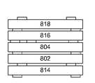
- FIG. 8A through FIG. 8Hillustrate stack creation using a variant of the above approaches.
- connectionsuch as described above, two chips 802 , 804 for the stack (whether still part of a wafer or after separation) ( FIG. 8A ) are brought together ( FIG. 8B ) and the temperature at the connection points 806 are raised to above the melting point of one of the two components 808 , 810 of the connections which contain one variant of materials suitable for the approach described herein.
- Thiswill cause an electrical connection to be formed at each of the connection points 806 and also change the composition of the electrically conductive bonding material to a new composition 812 that will have a higher melting point than the temperature used to create the composition.
- the joined chips 802 , 804can be cooled to a temperature below the connection forming temperature to cause the connection to “set.”
- a further chip 814can be brought to the now formed stack ( FIG. 8C ), its contacts (which also use a variant as described herein, and ideally the same variant used for joining the first two chips) can be brought into contact with mating contacts on the stack at their respective connection points.
- a subsequent raising of the temperature at these connection points to the connection forming temperaturewill cause the third chip to be connected to the stack ( FIG. 8D ) but, owing to the higher melting point of the composition created by the joining process, the connections between the first two chips will not be affected.
- This processcan be repeated again ( FIG. 8E , FIG. 8F ) and again ( FIG. 8G , FIG. 8H ), as many times as necessary to create the stack.
Landscapes
- Engineering & Computer Science (AREA)
- Microelectronics & Electronic Packaging (AREA)
- Computer Hardware Design (AREA)
- Power Engineering (AREA)
- Manufacturing & Machinery (AREA)
- Physics & Mathematics (AREA)
- Condensed Matter Physics & Semiconductors (AREA)
- General Physics & Mathematics (AREA)
- Wire Bonding (AREA)
- Contacts (AREA)
- Manufacturing Of Electrical Connectors (AREA)
- Connections Effected By Soldering, Adhesion, Or Permanent Deformation (AREA)
Abstract
Description
- This application is related to a U.S. patent application entitled “Mobile Binding In An Electronic Connection” filed concurrently herewith, the entirety of which is incorporated by reference as if fully set forth herein.
- The present invention relates to semiconductors and, more particularly, to electrical connections for such devices.
- When stacking chips, there are essentially two ways that chip to chip connections can be formed. One way, is to form the complete stack and then concurrently subject the entire stack to the conditions, such as heating and cooling, required to cause the electrically conductive bonding materials to establish the conductive path. The other way is to sequentially connect two components together, through heating and cooling of the connection points, and then sequentially attaching the next chip in the same manner, and so on, until the stack is complete.
- The first, “concurrent” approach, has drawbacks because, in practice, it is difficult to maintain alignment among the stack components. In addition, it is difficult to ensure that all of the individual connections are each subjected to the appropriate conditions necessary to form reliable interconnections among the constituent components of the stack. Thus, there is a risk that any particular connection will not be made because the conditions near the connection were insufficient or detrimentally in excess of what was required.
- The second, “sequential” approach, does not have the alignment problem. However, it still has drawbacks because the heat used to join each chip after the first can adversely affect the connections of previously joined chips.
- Thus, there is a need for a better way of joining chips to form a stack that reduces or eliminates the problems that can be encountered by using conventional concurrent or sequential joining techniques.
- We have devised an approach that allows a stack of chips to be created (on a chip, die or wafer basis) through a sequential approach or a concurrent approach that does not suffer from the problems noted above.
- One aspect involves a method of creating an electrical connection. The method involves providing a pair of contacts each on one of two different chips, the pair of contacts defining a volume therebetween, the volume containing at least two compositions each having melting points, the compositions having been selected such that heating to a first temperature will cause a change in at least one of the at least two compositions such that the change will result in a new composition having a new composition melting point of a second temperature, greater than the first temperature and the melting point of at least a first of the at least two compositions, and heating the pair of contacts and the at least two compositions to the first temperature.
- Another aspect involves a stack of chips. The stack of chips has a first set of paired contacts electrically joining two chips together using a first material composition having a first melting point, and a set of contacts on one of the two chips including thereon a bonding constituent composition having a second melting point that is lower than the first melting point, so that when the set of contacts is mated with a corresponding set of contacts on a third chip and the set of contacts and corresponding set of contacts are heated, to a temperature between temperatures corresponding to the first and second melting points, the bonding constituent composition will become the first material composition.
- A further aspect involves a method performed on an electrical contact. The method involves heating at least two conductive materials located at a connection point to a first temperature, the first temperature being in excess of a temperature needed to cause at least some of a first of the at least two conductive materials to change to a state having a higher melting point than a melting point of the first of the at least two conductive materials, but lower than a liquidus temperature corresponding to a liquidus state on a state diagram for the first of the at least two conductive materials, and allowing the connection point to cool to below the temperature needed to cause the at least some of the first of the at least two conductive materials to change to the state having the higher melting point.
- The advantages and features described herein are a few of the many advantages and features available from representative embodiments and are presented only to assist in understanding the invention. It should be understood that they are not to be considered limitations on the invention as defined by the claims, or limitations on equivalents to the claims. For instance, some of these advantages are mutually contradictory, in that they cannot be simultaneously present in a single embodiment. Similarly, some advantages are applicable to one aspect of the invention, and inapplicable to others. Thus, this summary of features and advantages should not be considered dispositive in determining equivalence. Additional features and advantages of the invention will become apparent in the following description, from the drawings, and from the claims.
FIG. 1 is a representation of the phase diagram for binary alloys of gold and tin;FIG. 2 is a cross sectional photograph of acontact 200 according to a variant of the approaches described herein;FIG. 3 is a cross sectional photograph of a similar original composition contact, such as shown inFIG. 2 , after it has been joined to a mating contact;FIG. 4 is a cross sectional photograph of a contact;FIG. 5 is a cross sectional photograph of a contact like fromFIG. 4 after it has been joined to another contact;FIG. 6 is a cross sectional photograph of a contact like fromFIG. 5 after completion of an elevated temperature exposure;FIG. 7 is a representation of the phase diagram for binary alloys of Pb and Sn; andFIG. 8A throughFIG. 8H , which illustrate stack creation using a variant of the above approaches.- U.S. patent applications, Ser. Nos. 11/329,481, 11/329,506, 11/329,539, 11/329,540, 11/329,556, 11/329,557, 11/329,558, 11/329,574, 11/329,575, 11/329,576, 11/329,873, 11/329,874, 11/329,875, 11/329,883, 11/329,885, 11/329,886, 11/329,887, 11/329,952, 11/329,953, 11/329,955, 11/330,011 and 11/422,551, incorporated herein by reference describe various techniques for forming small, deep vias in, and electrical contacts for, semiconductor wafers. These techniques allow for via densities and placement that was previously unachievable and can be performed on a chip, die or wafer scale.
- The techniques described therein are, as described, particularly well suited for use in creating very compact stacks of chips. Moreover, those techniques can involve use of a “tack & fuse” process that provides further advantages independent of many of the techniques described therein.
- In addition, U.S. patent application entitled “Mobile Binding In An Electronic Connection” filed concurrently herewith and incorporated herein by reference, describes ways to reduce or eliminate the problem of phase segregation in connections. As will become apparent, that approach is completely compatible with the techniques described herein and, in doing so, further advantages can be achieved that are not obtained with either one by themselves.
- Specifically, we have devised a further improvement to those techniques that allows a stack of chips to be created (on a chip, die or wafer basis) through a sequential approach or a concurrent approach that does not suffer from the problems noted above. In addition, in some implementations, we take advantage of the use of specific barriers with specific bonding materials to prevent mobile atoms from creating phase segregation or voids. This is accomplished by specifically selecting bonding materials used, based upon the temperature at which the bonding materials flow, to allow multiple high-temperature processing steps to occur without detrimentally affecting any previously formed connections.
- This can be accomplished in different ways. However, in general the approach involves selecting the particular materials that will be part of the electrical connection formation (whether they are pure, substantially pure or alloyed metals) such that the initial formation of an electrically conductive connection will occur at about a particular temperature “T1”. However, as a result of that formation, the materials that form the conductive connection will change into a composition that has a higher melting point than that of the original materials. As a result, a subsequent connection that is created using the same materials will not cause the original connection to begin to liquify (or if the new melting point is higher than T1, but very close to T1, such that no minimally present original materials appreciably liquify).
- Optionally, the materials can have been selected so that subsequent elevation to a higher temperature “T2” will cause a further change into a composition with yet a higher melting point. In this manner, subsequent elevations in temperature to T1 will have no effect at all.
- Advantageously, this approach is particularly useful in conjunction with a tack & fuse connection process, because it already involves a lower temperature “tack” phase and a subsequent higher temperature “fuse” phase.
- One example of this approach is illustrated with respect to
FIG. 1 throughFIG. 3 . - In this example, an alloy is deposited on a contact. In this example, the deposited alloy is an alloy of gold and tin, specifically, 80% Au and 20% Sn.
FIG. 1 is a representation of the phase diagram100 for binary alloys of gold and tin (although not precisely shown to scale). As can be seen this 80/20 AuSn alloy is at aeutectic point 102 of the phase diagram100. Thiseutectic point 102 represents the lowest melting point of this composition alloy. However, as the alloy is taken to a higher temperature the alloy interacts with some other material that is present, for example, the contact material or, preferably, a material that was deposited either i) between the contact and the alloy, or ii) on top of the alloy, to cause a compositional change of the alloy. Depending upon the interaction and materials, this compositional change will cause movement to the right or left on the phase diagram based upon which of the weight percentage component concentrations decrease or increase. As long as the composition does not cause a shift on the phase diagram to a composition of lower melting point, the result is a composition that has a higher melting point than the starting composition. - Depending upon the particular implementation, this left or right movement on the phase diagram can be the result of addition of one of the constituent components, removal of one of the constituent components, or addition of one or more other components.
- By way of one example, a pure tin or high tin concentration gold-tin layer could have been deposited on top of the alloy. Thus, when the melting temperature of the main gold-tin alloy was reached, the additional tin or gold-tin alloy will also have melted and combined with the 80/20 alloy to form a new concentration that was higher in tin, for example a 70/30 gold-tin alloy. This concentration is to the right of the original composition and thus, has a higher melting point than the 80/20 alloy.
- Alternatively, a material could have been used that would draw tin out of the gold-tin alloy and itself alloy with the tin leaving a higher concentration of gold, for example. This would result in leftward movement on the phase diagram due to the higher concentration of gold and, hence, a higher melting point for the resultant alloy.
- In the case of the 80/20 gold-tin alloy, looking at the phase diagram, to achieve the desired result, the compositional change could be one that added tin or removed gold to cause rightward compositional movement on the phase diagram or removed tin or added gold to cause leftward compositional movement on the phase diagram.
- In another similar alternative, a material could be used that will alloy with both the gold and tin to itself create a small amount of ternary alloy and, as long as the composition of the main alloy changed such that it had a higher melting point, the same effect would be achieved.
- By way of a similar example with reference to
FIG. 2 andFIG. 3 presume that the same approach and materials as above were used (i.e. 80/20 Au—Sn), but a sufficient volume of nickel was deposited, for example, under the alloy as a barrier between the alloy and the contact, or on top of the alloy as a cap.FIG. 2 is a cross sectional photograph of acontact 200 according to a variant of the approaches described herein having a connection material202 (the 80/20 Au—Sn alloy) deposited on top of the barrier material204 (the Ni barrier). In such a case, at an elevated temperature of or above about 300° C., the materials will diffuse to some extent. The result will be that tin atoms will be absorbed by, or alloy with, the Ni layer leaving behind a Au—Sn alloy composition with a high percentage of the lower mobility species (in this case gold) while the nickel has trapped some of the higher mobility tin and absorbed the remainder of it. FIG. 3 is a cross sectional photograph of a similaroriginal composition contact 302, such as shown inFIG. 2 , after it has been joined to amating contact 304 at an elevated temperature, as discussed above, to form an electrically conductive connection between the twocontacts FIG. 3 , as a result of the above approach, the new composition within the volume between thecontact pair areas 306 have 97% gold while someareas 308 have 25% tin. As a result, from the phase diagram100 ofFIG. 1 , it should be evident that the melting point of the various resulting materials has changed dramatically. Moreover, due to the fact that a substantial part of the contact is now more than 95% gold, the majority of the contact will have a melting point closer to 1000° C. than to 300° C. Even those regions with higher tin concentrations will have melting points closer to 400° C. than 300° C.- Still further, and advantageously, the addition of nickel into the compositional mix makes the tin less likely to be mobile. This means that the likelihood of a phase segregation problem is a reduced.
- Advantageously, in addition, the absorption or alloying of the tin prevents the entire mix from becoming self-centering, what we and the above-incorporated applications call a “liquidous” or “liquidus” state which is different from the liquidus state referred to in a phase.
- Note, however, that it is possible for the connections of some implementations to soften to something less that a liquidus state on a phase diagram (i.e. the melting point) for the material or some component thereof, for example, with a post and penetration connection approach, the “malleable” material may need to be at an elevated temperature to allow the material to soften sufficiently to allow the post to penetrate but not soften to the “liquidus” state as we have defined it, let alone to a molten state.
- As a result, the contact can be raised up to the original melting point over and over again without having any effect on this connection. Thus, it should be appreciated that this approach could be used over and over to add chips to a stack without concern that the forming of the new connections will disrupt the prior connections.
- Of course, it should now be appreciated that the starting composition need not be one at the lowest melting point, so long as the compositional change results in an upwards shift in melting point. This can be seen from the following example where the materials start off segregated and then combine into a final state.
FIG. 4 is a cross sectional photograph of acontact 400 according to one variant that is made up of abarrier 402, in this case nickel, on top of adevice pad 404 covered by alayer 406 of 100% gold which, in turn, is covered by alayer 408 of 100% tin.- A contact like that of
FIG. 4 will be joined to another contact (not shown inFIG. 4 ) to form an electrical connection. In this example, the other contact will be a post that is covered by a layer of nickel. FIG. 5 is a cross sectional photograph of acontact 400 like fromFIG. 4 after it has been joined to theother contact 500 in a tack phase of a tack & fuse process.- Heating of the contact has caused the
layer 408 of tin, with its lower melting point, to diffuses into thelayer 406 of gold and through to thebarrier 402 of nickel. This changes the compositions so that there is still alayer 406 with a substantial amount of about 100% gold, but there is also now analloy layer 502 of about 80% gold and 20% tin instead of the original 100% tin layer. Thus, whereas the original compositions were located at points “C0” and “C1” on the phase diagram ofFIG. 1 , the gold layer is still at about point “C0”, but the new composition is now located at point “C2” on the phase diagram ofFIG. 1 so that, in the case of the tin to tin-alloy change, the melting point has gone up from about 232° C. to about 282° C. and the melting point of the gold has essentially not changed. (Of course in actuality, the composition of the gold might now be slightly less than 100%, thereby slightly lowering the melting point, but it would be an insubstantial change because the meaningful temperature would be between about 232° C. and about 282° C.). Referring back toFIG. 5 , if thatcontact pair FIG. 6 is a cross sectional photograph of a contact like fromFIG. 5 after completion of a process of elevated temperature exposure, by way of example, a fuse process. As can be seen inFIG. 6 , the final composition of the connection is now a mostly gold (about 98%)center area 602 flanked by a ternary alloy604 of gold, tin and nickel, in this example, of approximately 45% Au, 35% Sn and 20% Ni. Since this alloy604 has a higher melting point than the 80%/20% gold-tin alloy, the same effect described above has been obtained. Thus, this contact could be subjected to heat cycling up to the temperature that caused this ternary alloy604 to form, without the risk of this connection being disrupted because the component melting points are all above that temperature.- At this point it is worth noting that the above approach is not limited to use with pure metals or alloys. The same approach can be used for solders (whether they include lead or are lead free).
FIG. 7 is a representation of the phase diagram700 for binary alloys of lead and tin (although not precisely shown to scale). Bearing the above description and examples in mind, one can now see that if an initial composition coinciding with theeutectic point 702 is used and an additional composition is used to either add lead or remove tin, the melting point will go up as the composition moves to the left side of the phase diagram. Alternatively, with thatsame starting point 702, if an additional composition can is used to either remove lead or add tin, the melting point will still go up by virtue of the composition moving to the right side of the phase diagram700.- It should now be appreciated that the same approach can advantageously even be used with conventional C4 solder which, as indicated on the phase diagram, has approximately a 60%Pb/40%Sn composition. To do so, as it should now be evident, an additional composition is used that will remove tin or add lead to the C4 solder upon heating. In this manner, the compositional change will result in a point to the left of the composition of C4 solder and, consequently a higher melting point. If one presumes that this is done for a connection and the resulting composition is 25% tin and 75% lead, the melting point will have gone up from the temperature TC4 to the temperature corresponding to the point on the phase diagram labeled “TN”. Thereafter, the temperature of the connection can go up to and above the C4 melting point and, as long as it does not exceed the TN point temperature, the connection will not be disturbed.
- Now, it can be appreciated that, by using a variant of this approach, a stack800 of chips can be easily created in a sequential manner as follows. This process is illustrated, in overly simplified form, in
FIG. 8A throughFIG. 8H , which illustrate stack creation using a variant of the above approaches. - Using a connection such as described above, two
chips FIG. 8A ) are brought together (FIG. 8B ) and the temperature at the connection points806 are raised to above the melting point of one of the twocomponents new composition 812 that will have a higher melting point than the temperature used to create the composition. Then, the joinedchips further chip 814 can be brought to the now formed stack (FIG. 8C ), its contacts (which also use a variant as described herein, and ideally the same variant used for joining the first two chips) can be brought into contact with mating contacts on the stack at their respective connection points. A subsequent raising of the temperature at these connection points to the connection forming temperature will cause the third chip to be connected to the stack (FIG. 8D ) but, owing to the higher melting point of the composition created by the joining process, the connections between the first two chips will not be affected. This process can be repeated again (FIG. 8E ,FIG. 8F ) and again (FIG. 8G ,FIG. 8H ), as many times as necessary to create the stack. - It should thus be understood that this description (including the figures) is only representative of some illustrative embodiments. For the convenience of the reader, the above description has focused on a representative sample of all possible embodiments, a sample that teaches the principles of the invention. The description has not attempted to exhaustively enumerate all possible variations. That alternate embodiments may not have been presented for a specific portion of the invention, or that further undescribed alternate embodiments may be available for a portion, is not to be considered a disclaimer of those alternate embodiments. One of ordinary skill will appreciate that many of those undescribed embodiments incorporate the same principles of the invention and others are equivalent.
Claims (18)
Priority Applications (6)
| Application Number | Priority Date | Filing Date | Title |
|---|---|---|---|
| US11/696,774US7850060B2 (en) | 2007-04-05 | 2007-04-05 | Heat cycle-able connection |
| CN2008800110042ACN101652846B (en) | 2007-04-05 | 2008-06-05 | Recyclable thermal connection |
| JP2010501615AJP5702136B2 (en) | 2007-04-05 | 2008-06-05 | Heat cycle connection |
| KR1020097022730AKR20100012865A (en) | 2007-04-05 | 2008-06-05 | Heat cycle-able connection |
| PCT/IB2008/001436WO2008122890A2 (en) | 2007-04-05 | 2008-06-05 | Heat cycle-able connection |
| EP08762777AEP2313916A2 (en) | 2007-04-05 | 2008-06-05 | Heat cycle-able connection |
Applications Claiming Priority (1)
| Application Number | Priority Date | Filing Date | Title |
|---|---|---|---|
| US11/696,774US7850060B2 (en) | 2007-04-05 | 2007-04-05 | Heat cycle-able connection |
Publications (2)
| Publication Number | Publication Date |
|---|---|
| US20080245846A1true US20080245846A1 (en) | 2008-10-09 |
| US7850060B2 US7850060B2 (en) | 2010-12-14 |
Family
ID=39826084
Family Applications (1)
| Application Number | Title | Priority Date | Filing Date |
|---|---|---|---|
| US11/696,774Expired - Fee RelatedUS7850060B2 (en) | 2007-04-05 | 2007-04-05 | Heat cycle-able connection |
Country Status (6)
| Country | Link |
|---|---|
| US (1) | US7850060B2 (en) |
| EP (1) | EP2313916A2 (en) |
| JP (1) | JP5702136B2 (en) |
| KR (1) | KR20100012865A (en) |
| CN (1) | CN101652846B (en) |
| WO (1) | WO2008122890A2 (en) |
Cited By (1)
| Publication number | Priority date | Publication date | Assignee | Title |
|---|---|---|---|---|
| US20150170921A1 (en)* | 2013-12-17 | 2015-06-18 | Mitsubishi Electric Corporation | Method for manufacturing semiconductor device |
Families Citing this family (3)
| Publication number | Priority date | Publication date | Assignee | Title |
|---|---|---|---|---|
| US20090008430A1 (en)* | 2007-07-06 | 2009-01-08 | Lucent Technologies Inc. | Solder-bonding process |
| BRPI0914522B1 (en) | 2008-10-30 | 2019-04-02 | Evogene Ltd | METHOD FOR INCREASING YIELD, BIOMASS, GROWTH RATE, STRENGTH, OIL OTEOR, AND / OR EFFICIENCY OF NITROGEN USE OF A PLANT |
| JP6043058B2 (en) | 2011-11-07 | 2016-12-14 | デクセリアルズ株式会社 | Connection device, method for manufacturing connection structure, method for manufacturing chip stack component, and method for mounting electronic component |
Citations (64)
| Publication number | Priority date | Publication date | Assignee | Title |
|---|---|---|---|---|
| US3312878A (en)* | 1965-06-01 | 1967-04-04 | Ibm | High speed packaging of miniaturized circuit modules |
| US4418857A (en)* | 1980-12-31 | 1983-12-06 | International Business Machines Corp. | High melting point process for Au:Sn:80:20 brazing alloy for chip carriers |
| US4465223A (en)* | 1980-12-31 | 1984-08-14 | International Business Machines Corporation | Process for brazing |
| US4967950A (en)* | 1989-10-31 | 1990-11-06 | International Business Machines Corporation | Soldering method |
| US5100480A (en)* | 1990-04-18 | 1992-03-31 | Mitsubishi Denki Kabushiki Kaisha | Solar cell and method for manufacturing the same |
| US5220530A (en)* | 1990-08-07 | 1993-06-15 | Oki Electric Industry Co., Ltd. | Semiconductor memory element and method of fabricating the same |
| US5229315A (en)* | 1991-01-16 | 1993-07-20 | Gold Star Electron Co., Ltd. | Method for forming an isolated film on a semiconductor device |
| US5308784A (en)* | 1991-10-02 | 1994-05-03 | Samsung Electronics Co., Ltd. | Semiconductor device and method for making the same |
| US5349500A (en)* | 1992-08-19 | 1994-09-20 | Sheldahl, Inc. | Direct application of unpackaged integrated circuit to flexible printed circuit |
| US5399898A (en)* | 1992-07-17 | 1995-03-21 | Lsi Logic Corporation | Multi-chip semiconductor arrangements using flip chip dies |
| US5563084A (en)* | 1994-09-22 | 1996-10-08 | Fraunhofer-Gesellschaft zur F orderung der angewandten Forschung e.V. | Method of making a three-dimensional integrated circuit |
| US5587119A (en)* | 1994-09-14 | 1996-12-24 | E-Systems, Inc. | Method for manufacturing a coaxial interconnect |
| US5608264A (en)* | 1995-06-05 | 1997-03-04 | Harris Corporation | Surface mountable integrated circuit with conductive vias |
| US5708569A (en)* | 1993-04-07 | 1998-01-13 | Zycon Corporation | Annular circuit components coupled with printed circuit board through-hole |
| US5780776A (en)* | 1996-05-31 | 1998-07-14 | Nec Corporation | Multilayer circuit board unit |
| US5814889A (en)* | 1995-06-05 | 1998-09-29 | Harris Corporation | Intergrated circuit with coaxial isolation and method |
| US5872338A (en)* | 1996-04-10 | 1999-02-16 | Prolinx Labs Corporation | Multilayer board having insulating isolation rings |
| US5929524A (en)* | 1995-12-14 | 1999-07-27 | Nec Corporation | Semiconductor device having ring-shaped conductive spacer which connects wiring layers |
| US5962922A (en)* | 1998-03-18 | 1999-10-05 | Wang; Bily | Cavity grid array integrated circuit package |
| US5973396A (en)* | 1996-02-16 | 1999-10-26 | Micron Technology, Inc. | Surface mount IC using silicon vias in an area array format or same size as die array |
| US6037665A (en)* | 1997-03-03 | 2000-03-14 | Nec Corporation | Mounting assembly of integrated circuit device and method for production thereof |
| US6075710A (en)* | 1998-02-11 | 2000-06-13 | Express Packaging Systems, Inc. | Low-cost surface-mount compatible land-grid array (LGA) chip scale package (CSP) for packaging solder-bumped flip chips |
| US6184066B1 (en)* | 1997-05-28 | 2001-02-06 | Matsushita Electric Industrial Co., Ltd. | Method for fabricating semiconductor device |
| US6215114B1 (en)* | 1997-09-25 | 2001-04-10 | Canon Kk | Optical probe for detecting or irradiating light and near-field optical microscope having such probe and manufacturing method of such probe |
| US20010001292A1 (en)* | 1998-04-07 | 2001-05-17 | Bertin Claude Louis | Through-chip conductors for low inductance chip-to-chip integration and off-chip connections |
| US20010033509A1 (en)* | 1998-11-23 | 2001-10-25 | Micron Technology, Inc. | Stacked integrated circuits |
| US6316737B1 (en)* | 1999-09-09 | 2001-11-13 | Vlt Corporation | Making a connection between a component and a circuit board |
| US20010048166A1 (en)* | 2000-05-26 | 2001-12-06 | Takashi Miyazaki | Flip chip type semiconductor device and method of manufactruing the same |
| US20020017399A1 (en)* | 2000-08-11 | 2002-02-14 | Huey-Ru Chang | Coaxial via hole and process of fabricating the same |
| US20020027441A1 (en)* | 1996-04-01 | 2002-03-07 | Salman Akram | Semiconductor test interconnect with variable flexure contacts |
| US20020094675A1 (en)* | 1998-09-02 | 2002-07-18 | Robert Kerr | Methods of contacting lines and methods of forming an electrical contact in a semiconductor device |
| US20020102835A1 (en)* | 2000-09-07 | 2002-08-01 | Michele Stucchi | Method of fabrication and device for electromagnetic-shielding structures in a damascene-based interconnect scheme |
| US20020127761A1 (en)* | 2000-12-20 | 2002-09-12 | Stmicroelectronics S.R.I. | Process for manufacturing components in a semiconductor material wafer with reduction in the starting wafer thickness |
| US20020134581A1 (en)* | 2000-03-31 | 2002-09-26 | Intel Corporation | Hybrid capacitor, circuit, and system |
| US6498089B2 (en)* | 2001-03-09 | 2002-12-24 | Fujitsu Limited | Semiconductor integrated circuit device with moisture-proof ring and its manufacture method |
| US20030047799A1 (en)* | 2001-01-10 | 2003-03-13 | Raytheon Company | Wafer level interconnection |
| US20030052324A1 (en)* | 2001-08-09 | 2003-03-20 | Hajime Kimura | Semiconductor device |
| US20030080408A1 (en)* | 1997-12-18 | 2003-05-01 | Farnworth Warren M. | Method for fabricating semiconductor components and interconnects with contacts on opposing sides |
| US6559540B2 (en)* | 2000-02-09 | 2003-05-06 | Nec Electronics Corporation | Flip-chip semiconductor device and method of forming the same |
| US20030085471A1 (en)* | 2001-11-07 | 2003-05-08 | Takahiro Iijima | Semiconductor package and method of production thereof |
| US6577013B1 (en)* | 2000-09-05 | 2003-06-10 | Amkor Technology, Inc. | Chip size semiconductor packages with stacked dies |
| US6590278B1 (en)* | 2002-01-08 | 2003-07-08 | International Business Machines Corporation | Electronic package |
| US6599778B2 (en)* | 2001-12-19 | 2003-07-29 | International Business Machines Corporation | Chip and wafer integration process using vertical connections |
| US20030159262A1 (en)* | 2002-02-22 | 2003-08-28 | Eliezer Pasternak | High frequency device packages and methods |
| US20030206680A1 (en)* | 2002-05-03 | 2003-11-06 | Georgia Tech Research Corporation | Devices having compliant wafer-level input/output interconnections and packages using pillars and methods of fabrication thereof |
| US6706554B2 (en)* | 2000-10-26 | 2004-03-16 | Oki Electric Industry Co., Ltd. | Conductor posts, construction for and method of fabricating semiconductor integrated circuit chips using the conductor post, and method of probing semiconductor integrated circuit chips |
| US20040051168A1 (en)* | 2002-06-25 | 2004-03-18 | Matsushita Electric Industrial Co., Ltd. | Semiconductor device and method for manufacturing the same |
| US6740576B1 (en)* | 2000-10-13 | 2004-05-25 | Bridge Semiconductor Corporation | Method of making a contact terminal with a plated metal peripheral sidewall portion for a semiconductor chip assembly |
| US20040124523A1 (en)* | 2002-06-18 | 2004-07-01 | Poo Chia Yong | Semiconductor devices including peripherally located bond pads, intermediates thereof, assemblies, and packages including the semiconductor devices, and support elements for the semiconductor devices |
| US20040207061A1 (en)* | 2001-08-30 | 2004-10-21 | Farrar Paul A. | Multi-chip electronic package and cooling system |
| US20040256686A1 (en)* | 2003-04-08 | 2004-12-23 | Stmicroelectronics S.R.L. | Method for manufacturing a micro-electro-mechanical device, in particular an optical microswitch, and micro-electro-mechanical device thus obtained |
| US20040262635A1 (en)* | 2003-06-24 | 2004-12-30 | Sang-Yun Lee | Three-dimensional integrated circuit structure and method of making same |
| US20050006789A1 (en)* | 2003-06-16 | 2005-01-13 | Kabushiki Kaisha Toshiba | Packaging assembly and method of assembling the same |
| US20050046034A1 (en)* | 2003-09-03 | 2005-03-03 | Micron Technology, Inc. | Apparatus and method for high density multi-chip structures |
| US20050104219A1 (en)* | 2003-09-26 | 2005-05-19 | Kuniyasu Matsui | Intermediate chip module, semiconductor device, circuit board, and electronic device |
| US20050104027A1 (en)* | 2003-10-17 | 2005-05-19 | Lazarev Pavel I. | Three-dimensional integrated circuit with integrated heat sinks |
| US20050121768A1 (en)* | 2003-12-05 | 2005-06-09 | International Business Machines Corporation | Silicon chip carrier with conductive through-vias and method for fabricating same |
| US20050133930A1 (en)* | 2003-12-17 | 2005-06-23 | Sergey Savastisuk | Packaging substrates for integrated circuits and soldering methods |
| US20050146049A1 (en)* | 2003-12-24 | 2005-07-07 | Agency For Science, Technology And Research | RF and MMIC stackable micro-modules |
| US6939789B2 (en)* | 2002-05-13 | 2005-09-06 | Taiwan Semiconductor Manufacturing Co., Ltd. | Method of wafer level chip scale packaging |
| US20060134832A1 (en)* | 2004-12-21 | 2006-06-22 | Renesas Technology Corp. | Manufacturing method of semiconductor device |
| US20060278992A1 (en)* | 2005-06-14 | 2006-12-14 | John Trezza | Post & penetration interconnection |
| US7157310B2 (en)* | 2004-09-01 | 2007-01-02 | Micron Technology, Inc. | Methods for packaging microfeature devices and microfeature devices formed by such methods |
| US7400042B2 (en)* | 2005-05-03 | 2008-07-15 | Rosemount Aerospace Inc. | Substrate with adhesive bonding metallization with diffusion barrier |
Family Cites Families (6)
| Publication number | Priority date | Publication date | Assignee | Title |
|---|---|---|---|---|
| EP0516866A1 (en) | 1991-05-03 | 1992-12-09 | International Business Machines Corporation | Modular multilayer interwiring structure |
| US5872051A (en) | 1995-08-02 | 1999-02-16 | International Business Machines Corporation | Process for transferring material to semiconductor chip conductive pads using a transfer substrate |
| JP4608763B2 (en) | 2000-11-09 | 2011-01-12 | 日本電気株式会社 | Semiconductor device |
| SG111972A1 (en) | 2002-10-17 | 2005-06-29 | Agency Science Tech & Res | Wafer-level package for micro-electro-mechanical systems |
| US7390735B2 (en) | 2005-01-07 | 2008-06-24 | Teledyne Licensing, Llc | High temperature, stable SiC device interconnects and packages having low thermal resistance |
| WO2006138492A2 (en) | 2005-06-14 | 2006-12-28 | Cubic Wafer, Inc. | Post & penetration interconnection |
- 2007
- 2007-04-05USUS11/696,774patent/US7850060B2/ennot_activeExpired - Fee Related
- 2008
- 2008-06-05WOPCT/IB2008/001436patent/WO2008122890A2/enactiveApplication Filing
- 2008-06-05KRKR1020097022730Apatent/KR20100012865A/ennot_activeCeased
- 2008-06-05EPEP08762777Apatent/EP2313916A2/ennot_activeWithdrawn
- 2008-06-05JPJP2010501615Apatent/JP5702136B2/ennot_activeExpired - Fee Related
- 2008-06-05CNCN2008800110042Apatent/CN101652846B/enactiveActive
Patent Citations (66)
| Publication number | Priority date | Publication date | Assignee | Title |
|---|---|---|---|---|
| US3312878A (en)* | 1965-06-01 | 1967-04-04 | Ibm | High speed packaging of miniaturized circuit modules |
| US4418857A (en)* | 1980-12-31 | 1983-12-06 | International Business Machines Corp. | High melting point process for Au:Sn:80:20 brazing alloy for chip carriers |
| US4465223A (en)* | 1980-12-31 | 1984-08-14 | International Business Machines Corporation | Process for brazing |
| US4967950A (en)* | 1989-10-31 | 1990-11-06 | International Business Machines Corporation | Soldering method |
| US5100480A (en)* | 1990-04-18 | 1992-03-31 | Mitsubishi Denki Kabushiki Kaisha | Solar cell and method for manufacturing the same |
| US5220530A (en)* | 1990-08-07 | 1993-06-15 | Oki Electric Industry Co., Ltd. | Semiconductor memory element and method of fabricating the same |
| US5229315A (en)* | 1991-01-16 | 1993-07-20 | Gold Star Electron Co., Ltd. | Method for forming an isolated film on a semiconductor device |
| US5308784A (en)* | 1991-10-02 | 1994-05-03 | Samsung Electronics Co., Ltd. | Semiconductor device and method for making the same |
| US5399898A (en)* | 1992-07-17 | 1995-03-21 | Lsi Logic Corporation | Multi-chip semiconductor arrangements using flip chip dies |
| US5349500A (en)* | 1992-08-19 | 1994-09-20 | Sheldahl, Inc. | Direct application of unpackaged integrated circuit to flexible printed circuit |
| US5708569A (en)* | 1993-04-07 | 1998-01-13 | Zycon Corporation | Annular circuit components coupled with printed circuit board through-hole |
| US5587119A (en)* | 1994-09-14 | 1996-12-24 | E-Systems, Inc. | Method for manufacturing a coaxial interconnect |
| US5563084A (en)* | 1994-09-22 | 1996-10-08 | Fraunhofer-Gesellschaft zur F orderung der angewandten Forschung e.V. | Method of making a three-dimensional integrated circuit |
| US5608264A (en)* | 1995-06-05 | 1997-03-04 | Harris Corporation | Surface mountable integrated circuit with conductive vias |
| US5814889A (en)* | 1995-06-05 | 1998-09-29 | Harris Corporation | Intergrated circuit with coaxial isolation and method |
| US5929524A (en)* | 1995-12-14 | 1999-07-27 | Nec Corporation | Semiconductor device having ring-shaped conductive spacer which connects wiring layers |
| US5973396A (en)* | 1996-02-16 | 1999-10-26 | Micron Technology, Inc. | Surface mount IC using silicon vias in an area array format or same size as die array |
| US20020027441A1 (en)* | 1996-04-01 | 2002-03-07 | Salman Akram | Semiconductor test interconnect with variable flexure contacts |
| US5872338A (en)* | 1996-04-10 | 1999-02-16 | Prolinx Labs Corporation | Multilayer board having insulating isolation rings |
| US5780776A (en)* | 1996-05-31 | 1998-07-14 | Nec Corporation | Multilayer circuit board unit |
| US6037665A (en)* | 1997-03-03 | 2000-03-14 | Nec Corporation | Mounting assembly of integrated circuit device and method for production thereof |
| US6184066B1 (en)* | 1997-05-28 | 2001-02-06 | Matsushita Electric Industrial Co., Ltd. | Method for fabricating semiconductor device |
| US6215114B1 (en)* | 1997-09-25 | 2001-04-10 | Canon Kk | Optical probe for detecting or irradiating light and near-field optical microscope having such probe and manufacturing method of such probe |
| US20030080408A1 (en)* | 1997-12-18 | 2003-05-01 | Farnworth Warren M. | Method for fabricating semiconductor components and interconnects with contacts on opposing sides |
| US6075710A (en)* | 1998-02-11 | 2000-06-13 | Express Packaging Systems, Inc. | Low-cost surface-mount compatible land-grid array (LGA) chip scale package (CSP) for packaging solder-bumped flip chips |
| US5962922A (en)* | 1998-03-18 | 1999-10-05 | Wang; Bily | Cavity grid array integrated circuit package |
| US20010001292A1 (en)* | 1998-04-07 | 2001-05-17 | Bertin Claude Louis | Through-chip conductors for low inductance chip-to-chip integration and off-chip connections |
| US20020094675A1 (en)* | 1998-09-02 | 2002-07-18 | Robert Kerr | Methods of contacting lines and methods of forming an electrical contact in a semiconductor device |
| US6314013B1 (en)* | 1998-11-23 | 2001-11-06 | Micron Technology, Inc. | Stacked integrated circuits |
| US20010033509A1 (en)* | 1998-11-23 | 2001-10-25 | Micron Technology, Inc. | Stacked integrated circuits |
| US6316737B1 (en)* | 1999-09-09 | 2001-11-13 | Vlt Corporation | Making a connection between a component and a circuit board |
| US6559540B2 (en)* | 2000-02-09 | 2003-05-06 | Nec Electronics Corporation | Flip-chip semiconductor device and method of forming the same |
| US20020134581A1 (en)* | 2000-03-31 | 2002-09-26 | Intel Corporation | Hybrid capacitor, circuit, and system |
| US20010048166A1 (en)* | 2000-05-26 | 2001-12-06 | Takashi Miyazaki | Flip chip type semiconductor device and method of manufactruing the same |
| US20020017399A1 (en)* | 2000-08-11 | 2002-02-14 | Huey-Ru Chang | Coaxial via hole and process of fabricating the same |
| US6577013B1 (en)* | 2000-09-05 | 2003-06-10 | Amkor Technology, Inc. | Chip size semiconductor packages with stacked dies |
| US20020102835A1 (en)* | 2000-09-07 | 2002-08-01 | Michele Stucchi | Method of fabrication and device for electromagnetic-shielding structures in a damascene-based interconnect scheme |
| US6740576B1 (en)* | 2000-10-13 | 2004-05-25 | Bridge Semiconductor Corporation | Method of making a contact terminal with a plated metal peripheral sidewall portion for a semiconductor chip assembly |
| US6706554B2 (en)* | 2000-10-26 | 2004-03-16 | Oki Electric Industry Co., Ltd. | Conductor posts, construction for and method of fabricating semiconductor integrated circuit chips using the conductor post, and method of probing semiconductor integrated circuit chips |
| US20020127761A1 (en)* | 2000-12-20 | 2002-09-12 | Stmicroelectronics S.R.I. | Process for manufacturing components in a semiconductor material wafer with reduction in the starting wafer thickness |
| US20030047799A1 (en)* | 2001-01-10 | 2003-03-13 | Raytheon Company | Wafer level interconnection |
| US6498089B2 (en)* | 2001-03-09 | 2002-12-24 | Fujitsu Limited | Semiconductor integrated circuit device with moisture-proof ring and its manufacture method |
| US20030052324A1 (en)* | 2001-08-09 | 2003-03-20 | Hajime Kimura | Semiconductor device |
| US20040207061A1 (en)* | 2001-08-30 | 2004-10-21 | Farrar Paul A. | Multi-chip electronic package and cooling system |
| US20030085471A1 (en)* | 2001-11-07 | 2003-05-08 | Takahiro Iijima | Semiconductor package and method of production thereof |
| US6599778B2 (en)* | 2001-12-19 | 2003-07-29 | International Business Machines Corporation | Chip and wafer integration process using vertical connections |
| US6590278B1 (en)* | 2002-01-08 | 2003-07-08 | International Business Machines Corporation | Electronic package |
| US20030159262A1 (en)* | 2002-02-22 | 2003-08-28 | Eliezer Pasternak | High frequency device packages and methods |
| US6770822B2 (en)* | 2002-02-22 | 2004-08-03 | Bridgewave Communications, Inc. | High frequency device packages and methods |
| US20030206680A1 (en)* | 2002-05-03 | 2003-11-06 | Georgia Tech Research Corporation | Devices having compliant wafer-level input/output interconnections and packages using pillars and methods of fabrication thereof |
| US6939789B2 (en)* | 2002-05-13 | 2005-09-06 | Taiwan Semiconductor Manufacturing Co., Ltd. | Method of wafer level chip scale packaging |
| US20040124523A1 (en)* | 2002-06-18 | 2004-07-01 | Poo Chia Yong | Semiconductor devices including peripherally located bond pads, intermediates thereof, assemblies, and packages including the semiconductor devices, and support elements for the semiconductor devices |
| US20040051168A1 (en)* | 2002-06-25 | 2004-03-18 | Matsushita Electric Industrial Co., Ltd. | Semiconductor device and method for manufacturing the same |
| US20040256686A1 (en)* | 2003-04-08 | 2004-12-23 | Stmicroelectronics S.R.L. | Method for manufacturing a micro-electro-mechanical device, in particular an optical microswitch, and micro-electro-mechanical device thus obtained |
| US20050006789A1 (en)* | 2003-06-16 | 2005-01-13 | Kabushiki Kaisha Toshiba | Packaging assembly and method of assembling the same |
| US20040262635A1 (en)* | 2003-06-24 | 2004-12-30 | Sang-Yun Lee | Three-dimensional integrated circuit structure and method of making same |
| US20050046034A1 (en)* | 2003-09-03 | 2005-03-03 | Micron Technology, Inc. | Apparatus and method for high density multi-chip structures |
| US20050104219A1 (en)* | 2003-09-26 | 2005-05-19 | Kuniyasu Matsui | Intermediate chip module, semiconductor device, circuit board, and electronic device |
| US20050104027A1 (en)* | 2003-10-17 | 2005-05-19 | Lazarev Pavel I. | Three-dimensional integrated circuit with integrated heat sinks |
| US20050121768A1 (en)* | 2003-12-05 | 2005-06-09 | International Business Machines Corporation | Silicon chip carrier with conductive through-vias and method for fabricating same |
| US20050133930A1 (en)* | 2003-12-17 | 2005-06-23 | Sergey Savastisuk | Packaging substrates for integrated circuits and soldering methods |
| US20050146049A1 (en)* | 2003-12-24 | 2005-07-07 | Agency For Science, Technology And Research | RF and MMIC stackable micro-modules |
| US7157310B2 (en)* | 2004-09-01 | 2007-01-02 | Micron Technology, Inc. | Methods for packaging microfeature devices and microfeature devices formed by such methods |
| US20060134832A1 (en)* | 2004-12-21 | 2006-06-22 | Renesas Technology Corp. | Manufacturing method of semiconductor device |
| US7400042B2 (en)* | 2005-05-03 | 2008-07-15 | Rosemount Aerospace Inc. | Substrate with adhesive bonding metallization with diffusion barrier |
| US20060278992A1 (en)* | 2005-06-14 | 2006-12-14 | John Trezza | Post & penetration interconnection |
Cited By (1)
| Publication number | Priority date | Publication date | Assignee | Title |
|---|---|---|---|---|
| US20150170921A1 (en)* | 2013-12-17 | 2015-06-18 | Mitsubishi Electric Corporation | Method for manufacturing semiconductor device |
Also Published As
| Publication number | Publication date |
|---|---|
| JP5702136B2 (en) | 2015-04-15 |
| CN101652846B (en) | 2013-04-24 |
| WO2008122890A2 (en) | 2008-10-16 |
| JP2011501394A (en) | 2011-01-06 |
| WO2008122890A3 (en) | 2009-02-12 |
| KR20100012865A (en) | 2010-02-08 |
| EP2313916A2 (en) | 2011-04-27 |
| US7850060B2 (en) | 2010-12-14 |
| CN101652846A (en) | 2010-02-17 |
Similar Documents
| Publication | Publication Date | Title |
|---|---|---|
| Tu et al. | Physics and materials challenges for lead-free solders | |
| US6342442B1 (en) | Kinetically controlled solder bonding | |
| TWI302722B (en) | Ubm pad, solder contact and methods for creating a solder joint | |
| CN1111822A (en) | Low temperature ternary C4 method | |
| JP5426081B2 (en) | Substrate bonding method and semiconductor device | |
| US7850060B2 (en) | Heat cycle-able connection | |
| JPH11192581A (en) | Soldering method | |
| KR101119761B1 (en) | Binding of constituents having a high mobility in an electronic connection | |
| US20020092895A1 (en) | Formation of a solder joint having a transient liquid phase by annealing and quenching | |
| CN103972115B (en) | Semiconductor device and the method manufacturing semiconductor device | |
| JP5035134B2 (en) | Electronic component mounting apparatus and manufacturing method thereof | |
| Holaday et al. | Transient liquid phase bonding | |
| EP1798763A1 (en) | Semiconductor device and die bonding method therefor | |
| Hu et al. | A Cu pillar bump bonding method using Au-Sn alloy cap as the interconnection layer | |
| CN102132390B (en) | Joint structure, joint material and method for producing joint material | |
| US11424217B2 (en) | Soldering a conductor to an aluminum layer | |
| Ou et al. | A study of electromigration in Sn3. 5Ag and Sn3. 8Ag0. 7Cu solder lines | |
| JP6287310B2 (en) | Electronic component, method for manufacturing electronic component, and method for manufacturing electronic device | |
| WO2011036829A1 (en) | Semiconductor device and process for production thereof | |
| US6609651B1 (en) | Method of soldering a leaded circuit component | |
| EP2858107A2 (en) | Semiconductor device with a bonding layer with a region comprising Ti and a region comprising Sn but with substantially no region comprising both Ti and Sn and method for manufacturing the same | |
| Bajwa et al. | Process development and material characterization of Cu-Cu thermo-compression bonding (TCB) for high-conductivity electrical interconnects. | |
| JP2016134421A (en) | Electronic device and method of manufacturing electronic device | |
| Kim et al. | Fluxless Sn-Ag Solder Joints between Silicon and Ag-Cladded Copper with Reliability Evaluations--MEJ | |
| Lee et al. | Microstructure evolution of Cu/Sn/Cu bonding stacks impacts on their mechanical properties |
Legal Events
| Date | Code | Title | Description |
|---|---|---|---|
| AS | Assignment | Owner name:CUBIC WAFER, INC., NEW HAMPSHIRE Free format text:ASSIGNMENT OF ASSIGNORS INTEREST;ASSIGNOR:TREZZA, JOHN;REEL/FRAME:019721/0356 Effective date:20070815 | |
| AS | Assignment | Owner name:CUFER ASSET LTD. L.L.C., DELAWARE Free format text:ASSIGNMENT OF ASSIGNORS INTEREST;ASSIGNOR:CUBIC WAFER, INC.;REEL/FRAME:020938/0143 Effective date:20080321 | |
| STCF | Information on status: patent grant | Free format text:PATENTED CASE | |
| FEPP | Fee payment procedure | Free format text:PAYOR NUMBER ASSIGNED (ORIGINAL EVENT CODE: ASPN); ENTITY STATUS OF PATENT OWNER: LARGE ENTITY | |
| CC | Certificate of correction | ||
| FPAY | Fee payment | Year of fee payment:4 | |
| MAFP | Maintenance fee payment | Free format text:PAYMENT OF MAINTENANCE FEE, 8TH YEAR, LARGE ENTITY (ORIGINAL EVENT CODE: M1552) Year of fee payment:8 | |
| FEPP | Fee payment procedure | Free format text:MAINTENANCE FEE REMINDER MAILED (ORIGINAL EVENT CODE: REM.); ENTITY STATUS OF PATENT OWNER: LARGE ENTITY | |
| LAPS | Lapse for failure to pay maintenance fees | Free format text:PATENT EXPIRED FOR FAILURE TO PAY MAINTENANCE FEES (ORIGINAL EVENT CODE: EXP.); ENTITY STATUS OF PATENT OWNER: LARGE ENTITY | |
| STCH | Information on status: patent discontinuation | Free format text:PATENT EXPIRED DUE TO NONPAYMENT OF MAINTENANCE FEES UNDER 37 CFR 1.362 | |
| FP | Lapsed due to failure to pay maintenance fee | Effective date:20221214 |